KNS120 - Educational electronic kit VELLEMAN - Free user manual and instructions
Find the device manual for free KNS120 VELLEMAN in PDF.

User questions about KNS120 VELLEMAN
0 question about this device. Answer the ones you know or ask your own.
Ask a new question about this device
Download the instructions for your Educational electronic kit in PDF format for free! Find your manual KNS120 - VELLEMAN and take your electronic device back in hand. On this page are published all the documents necessary for the use of your device. KNS120 by VELLEMAN.
USER MANUAL KNS120 VELLEMAN
natural_image
Cutaway illustration of an electronic device with components like battery, motor, and wiring (no text or symbols)USER MANUAL 2
HANDLEIDING 22
MODE D'EMPLOI 42
MANUAL DEL USUARIO 63
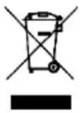
To all residents of the European Union
Important environmental information about this product
This symbol on the device or the package indicates that disposal of the device after its lifecycle could harm the environment. Do not dispose of the unit (or batteries) as unsorted municipal waste; it should be taken to a specialized company for recycling. This device should be returned to your distributor or to a local recycling service. Respect the local environmental rules.
If in doubt, contact your local waste disposal authorities.
Thank you for choosing Velleman! Please read the manual thoroughly before bringing this device into service. If the device was damaged in transit, do not install or use it and contact your dealer.
2. Safety Instructions

Read and understand this manual and all safety signs before using this appliance.
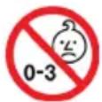
Choking hazard due to small parts. Not for children under 3 years.
8+
Recommended age: +.
- This product is intended for use for educational purposes in schools and other pedagogical contents under the surveillance of an adult instructor, such as science equipment.
- Protect from rain, moisture, splashing and dripping liquids, shocks and abuse, extreme heat and dust.
3. Warning
Adult supervision and assistance is required.
This unit is only for use by children aged 8 years and older.
Not suitable for children under age 3 years old due to small part(s) and component(s) – CHOKING HAZARD FROM INGESTION.
Read and follow all instructions in the manual before use.
This toy contains small parts and functional sharp points on components. Keep away from children under age 3 years.
2 x AA size batteries are required (not included).
Please retain the information and this manual for future reference.
Instructions for parents are included and have to be observed.
Do not use close to the ear! Misuse may cause damage to hearing.
4. Caution
Before setting up any experiment, please double check and make sure all wiring connections you have made are correct before inserting the batteries and switching on the unit, as failure may result in damage to components or circuit board unit.
When experiment is finished, make sure the batteries are disconnected and switch off the unit before you clear away the wires.
Do not apply any components or parts to the experiment other than those provided with this kit.
The toy is not to be connected to more than recommended number of power supplies.
User manual
Hair entanglement may result if the child's head is too close to the motorized unit of this toy. This toy contains functional sharp points on component leads and wires, requiring care when handling.
5. General Guidelines
• Refer to the Velleman® Service and Quality Warranty on the last pages of this manual.
- All modifications of the device are forbidden for safety reasons. Damage caused by user modifications to the device is not covered by the warranty.
- Only use the device for its intended purpose. Using the device in an unauthorised way will void the warranty.
- Damage caused by disregard of certain guidelines in this manual is not covered by the warranty and the dealer will not accept responsibility for any ensuing defects or problems.
- Nor Velleman group nv nor its dealers can be held responsible for any damage (extraordinary, incidental or indirect) – of any nature (financial, physical...) arising from the possession, use or failure of this product.
- Keep this manual for future reference.
6. Product description
We take pleasure to welcome you to try out this ready-to-use electronic circuit kit suitable for children of 8 years old and up. "You'll be amazed" to find what you can learn as the experiment is a realistic concept of electronics and electricity. It will definitely enable you to learn about the necessary electronic components, circuits, and theories as well as the basic electronics principles – electricity, voltage, current, resistance, magnetism, other electrical circuits and theories.
It is alright if you have no knowledge about electronics and do not fully understand how all the experiments work. Once you get started you will be able to build your understanding through experimenting and maybe trying out some interesting experiments on your own.
This electronic circuit kit contains more than 25 experiments, and it is smartly designed that the main circuit board unit has all the relevant electronic components included. All you have to do is simply connect the wires according to the wiring sequence of each experiment and follow the steps one by one. Once connected the circuit will activate and function.
Remember this is not a one-time experiment. The more you spend on building the experiments the better knowledge you will gain. You will never get bored but totally engaged as you will discover more new exciting experiments for a few years to come..
EXPERIMENTS
- Blower (Floating ball)
- Simple LED circuit
- Two LEDs in parallel connection
- Three LEDs in parallel connection
- Blower (Floating ball) and LED with separate switches
- Basic circuit operation of LEDs
- Demonstration of resistance and current
- Demonstration of the variable resistor
- Demonstration of the function of the capacitor
- Diode and capacitor discharge
- "AND Gate" circuit for LED
- "OR Gate" circuit for LED
- "NOT Gate" circuit for LED (with floating ball for extra excitement)
- "NAND Gate" circuit for LED (with floating ball for extra excitement)
- "NOR Gate" circuit for LED (with floating ball for extra excitement)
- A simple demonstration of the light sensor
- A simple demonstration of a function of the PNP transistor
- A simple demonstration of a function of the NPN transistor
- Delayed lighting up LED
User manual
- Delayed extinguishing LED
- Light control blower (Light type)
- Light control blower (Dark type)
- Alternating LED and blower
- Speed adjustable blower
- Connection indicator
- Manual control stop-and-resume blower
7. Glossary
Amplifier - An electronic circuit that amplifies the signal that is sent to it. The amplifying component can be a transistor, vacuum tube or appropriate magnetic device.
Battery - A source of energy. It contains chemicals which will undergo chemical reaction to produce electricity when a circuit is connected.
Capacitance - A measurement of the capacity of a capacitor for storing electric charge.
Capacitor - A device consists of two conductors that are separated by an insulator. It is designed for storing electrical charge or as a filter in a circuit.
IC (Integrated Circuit) - A small electronic device made of semiconductor material and is used for a variety of devices, including microprocessors, electronic equipment and automobiles.
Light Sensor - There are different types of light sensor. The one used here is a phototransistor. When light falls on it, it is like a switch connected and so current is allowed to pass through it.
Diode - A device used in electric circuitry to allow an electric current to flow in single direction and block it in the reverse direction.
Microphone - A device converts sound into an electrical signal.
Motor - A device converts electrical energy to mechanical motion.
LED (Light Emitting Diode) - A diode emits light when current is passing through it.
Resistance - A measurement of the degree to which an object opposes an electric current through it.
Resistor - A device designed for possessing resistance.
Speaker - A device that changes electrical signals into sound.
Switch - A device for opening and closing power source to a circuit.
Transistor - A semi-conductor device that amplifies a signal and opens or closes a circuit.
Truth Table - It is a mathematical table used to logically compute the values of logical explication and as a decision procedure.
Variable Resistor - A kind of resistor and a device of adjustable resistance in the electronic / electrical circuit.
Wire - A conductor that conducts electricity. Connecting a wire is like providing a path that allows electricity to flow though.
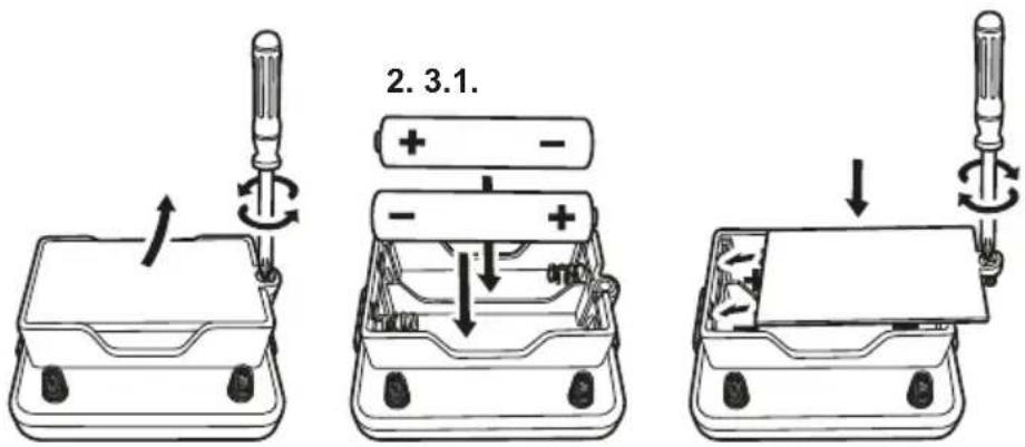
8. Battery Information
Use 2 x 1.5V AA size batteries (not included).
For best performance, always use fresh batteries and remove batteries when not in use.
Batteries must be inserted with the correct polarity.
Non-rechargeable batteries are not to be recharged.
Re-chargeable batteries are only to be charged under adult supervision.
Re-chargeable batteries are to be removed from the toy before being charged.
Different types of batteries or new and used batteries are not to be mixed.
Exhausted batteries are to be removed from the toy.
The supply terminals are not to be short-circuited.
Only batteries of the same or equivalent types are to be used.
Do not dispose of the batteries in fire.
Do not mix old and new batteries.
Do not mix alkaline, carbon zinc and re-chargeable batteries.
To insert batteries please unscrew battery cover with a screw driver. Insert the required batteries in accordance with battery polarity with + and - ends in the right position and then fix screw on the battery cover to close the battery compartment case.
text_image
2.3.1.9. Wiring sequence and connection
Ensure all wires are correctly connected to the numbered spring terminals of the main circuit board unit as stated wiring sequence of each experiment. Bend the spring terminal over and insert the exposed shiny conductor part of wire into spring terminal. Make sure the wire is securely connected to spring terminal.
For example if the wiring sequence is 4-33, 1-10-32-35, 2-12, then connect a wire between spring terminal 4 and 33; and then connect a wire between spring terminal 1 and 10, and a wire between spring terminal 10 and 32, and a wire between spring terminal 32 and 35; and finally connect a wire between spring terminal 2 and 12. This is an example for reference only, not an exact circuit connection in the experiment.
If the circuit does not work, you can check the wire and spring terminal connection whether it is not well connected or insulated plastic part of a wire is inserted to spring terminal.
10. Component characteristic
In this experiment kit, you will learn basic circuit theory, characteristic of capacitor, IC (Integrated Circuit), LED (Light Emitting Diode), light sensor, resistor and transistor. You can learn that when transistor and capacitor work together, various light and sound effects can be made in different circuit connections.
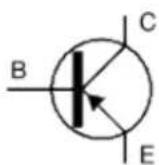
Capacitor is a device consists of two conductors that are separated by an insulator. It is designed for storing electrical charge or as a filter in a circuit. It is a commonly used component in electronic and electrical circuits as an energy storage device or as a filter device to filter out electronic noisy or useless frequency signals. There are various types of capacitor which are designed for different electronic / electrical circuit applications.
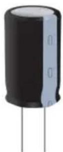
Electrolytic Capacitor

natural_image
Pure electrical circuit symbol for a capacitor, no text or labels presentCircuit symbol
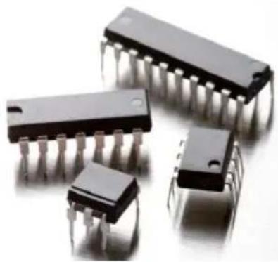
IC (Integrated Circuit) is a small electronic device made of semiconductors and is used for a variety of devices, including microprocessors, electronic equipment and automobiles. IC is made by a large number of transistors into a "chip" (silicon). It is now a critical and commonly used component in a wide variety of applications from toys, household products to state-of-the-art equipment.
User manual
natural_image
Close-up of four black integrated circuit chips with metallic pins, arranged in a row (no visible text or markings)Integrated Circuit
LED (Light Emitting Diode) is a diode which emits light when electric current passes through it. LED has various light colors which depend on what kind of semi-conducting materials are used. It is a commonly used device in household and vehicle lighting appliance.
LED (Light Emitting Diode)
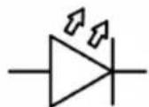
anode
Circuit symbol
Cathode
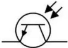
Light Sensor is a device that reacts to light. There are different types of light sensor. The one used here is a phototransistor. When there is no light, electric current cannot pass through it. And therefore it is like a switch that is switched off. When there is light falling on it, electric current can pass through it. It is then like a switch that is switched on. This way a light control circuit can be made.
natural_image
Pure electrical circuit symbol for a transistor without any text or labelsCircuit symbol
User manual
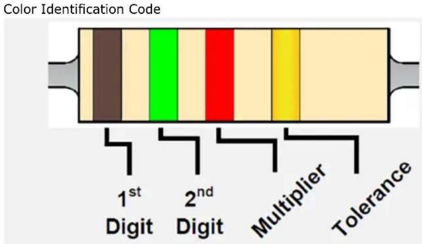
Resistor uses different color rings to represent the value (resistance). The 1st and 2nd rings represent the digit. The 3rd ring represents the multiplier as table shown. The 4th ring represents tolerance that means the precision of the resistance. Example: The color rings are Brown, Red, Brown and Gold which represents resistance is 120 ohm, tolerance 5% ( ).
text_image
Color Identification Code 1st Digit 2nd Digit Multiplier Tolerance| Color | 1st | 2nd | 3^rd - multiplier | Tolerance |
| Black | 0 | 0 | x 1 | |
| Brown | 1 | 1 | x 10 | |
| Red | 2 | 2 | x 100 | |
| Orange | 3 | 3 | x 1000 | |
| Yellow | 4 | 4 | x 10000 | |
| Green | 5 | 5 | x 100000 | |
| Blue | 6 | 6 | x 1000000 | |
| Purple | 7 | 7 | ||
| Grey | 8 | 8 | ||
| White | 9 | 9 | ||
| Brown | +/- 1% | |||
| Red | +/- 2% | |||
| Gold | x 0.1 | +/- 5% | ||
| Silver | x 0.01 | +/- 10% |
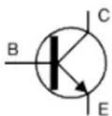
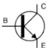
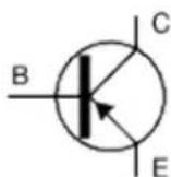
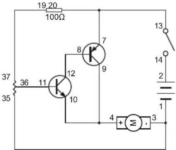
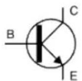
Transistor is a semi-conductor device that is used to amplify a signal and to open or close it in a circuit. There are two types of transistors, namely NPN and PNP, with similar circuit symbol. The transistor is a fundamental device commonly used in the modern electronic equipment. It has the fastest response and accurate action as amplifier and switching device, and can act as an individual device / component or as a part of IC (Integrated Circuit). IC is built of over a thousand to million transistors.
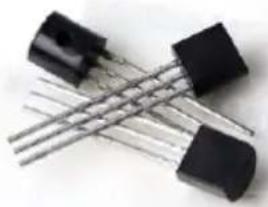
natural_image
Close-up of two black electronic components with metallic leads (no visible text or symbols)Transistor

NPN

PNP
Circuit symbol
If you have already read the above information and would like to understand more about electric circuit knowledge as well as how useful the components can be, then let's carry out the following experiments.
User manual
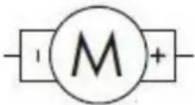
The motor is a device that produces rotary motion when electricity is provided. As an analogy, the battery is like a pump that pumps water through the piles (wires). When a circuit is connected, electricity can flow through it. The electricity flowing is called a current. A current is the flow of electric charges. The amount of a current is the amount of electric charge flowing in the wire in a second. Another common term we often heard about electricity is the voltage. Voltage is referring to the electric energy per unit charge. It is the electric energy of each unit amount of electric charge carries.
text_image
M11. Assembling
Blower:
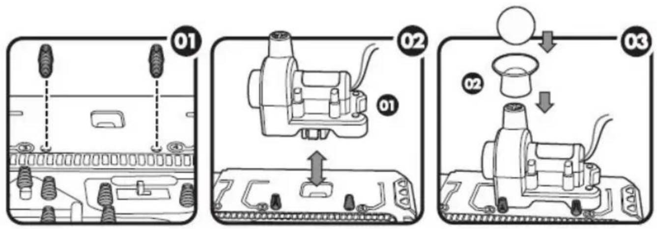
text_image
Diagram illustrating three steps of a device assembly or cleaning process, labeled 01, 02, and 03 with numbered components.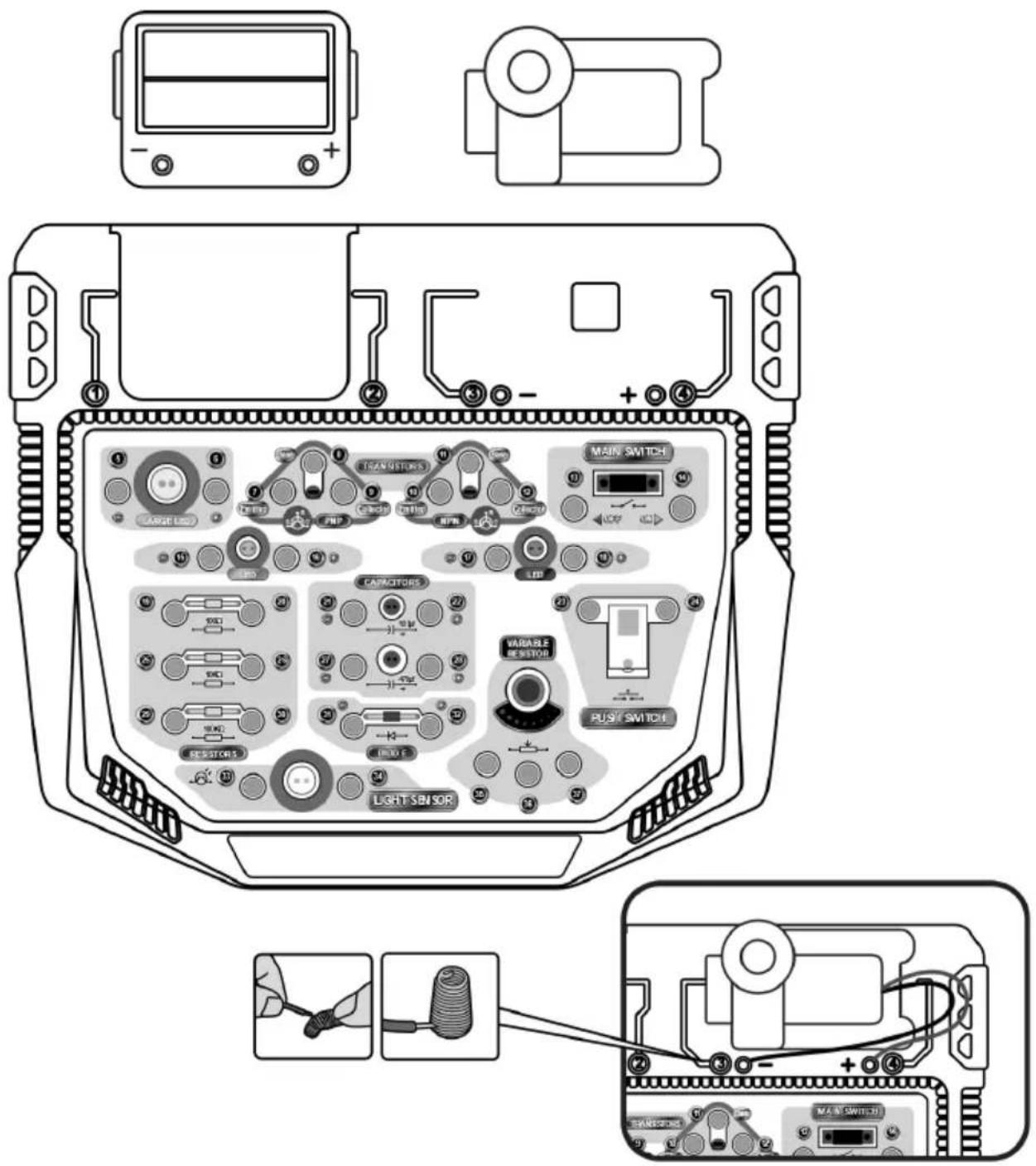
text_image
Diagram of a device rear panel with labeled components including transistors, main switch, and light sensor, plus wiring connections.User manual
12. Experiments
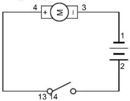
12.1 EXPERIMENT 1 - Blower (Floating ball)
Wiring Sequence
2-14, 13-4, 1-3
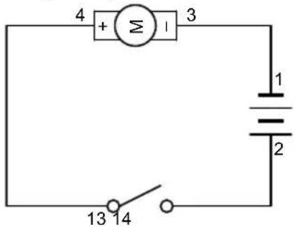
text_image
4 + Σ 1 3 1 2 13 14- Complete all wiring connections as indicated in the sequence.
- Switch on the main switch.
- The blower is on! Place the ball in mid-air to see it float!
12.2 EXPERIMENT Simple LED circuit
Wiring Sequence
2-6, 5-14, 13-1
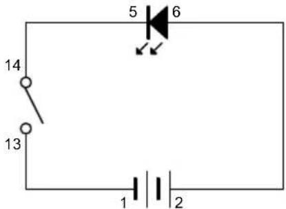
text_image
14 13 5 6 1 2- Complete all wiring connections as indicated in the sequence.
- Switch on the main switch.
- The LED will light up as illumination.
12.3 EXPERIMENT 3 - Two LEDs in parallel connection
Wiring Sequence
2-18-16, 17-15-13, 14-1
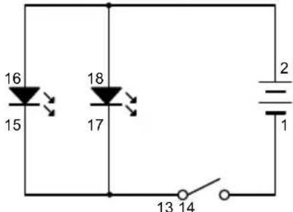
text_image
16 15 18 17 2 1 13 14- Complete all wiring connections as indicated in the sequence.
- Switch on the main switch to see both LEDs light up.
- When you switch off the main switch, both LEDs will be turned off.
User manual
12.4 EXPERIMENT 4 - Three LEDs in parallel connection
Wiring Sequence
2-18-16-6, 5-15-17-13, 14-1
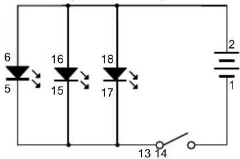
text_image
6 5 16 15 18 17 2 1 13 14- Complete all wiring connections as indicated in the sequence.
- Switch on the main switch to see all LEDs light up.
- When you switch off the main switch, all LEDs will be turned off.
12.5 EXPERIMENT 5 - Blower (Floating ball) and LED with separate switches
Wiring Sequence
2-4-6, 5-24, 3-14, 13-23-1
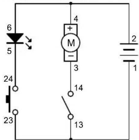
text_image
6 5 24 23 4 + M - 3 14 13 2 1- Complete all wiring connections as indicated in the sequence.
- Switch on the main switch. The blower will blow.
- Press the push switch, the LED will light up.
- The blower and the LED are controlled by separate switches. Therefore they can be turned ON and OFF separately.
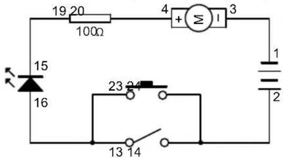
12.6 EXPERIMENT 6 - Basic circuit operation of LEDs
Wiring Sequence
2-14, 13-16-23, 24-19-15-6, 5-20-1
text_image
15 16 24 23 6 5 100Ω 19 20 1 2 13 14- Complete all wiring connections as indicated in the sequence.
- Switch on the main switch. You will see that the small LED will light up but the large LED will not.
User manual
- When you press the push switch, you will see the large LED will light up but the small LED will be turned off.
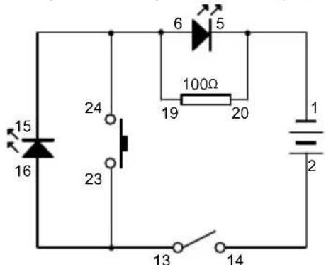
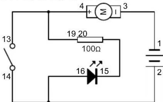
12.7 EXPERIMENT 7 - Demonstration of resistance and current
Wiring Sequence
2-23-13, 14-25, 24-19, 20-26-18, 17-1
text_image
18 17 1 2 100Ω 20 19 24 23 10kΩ 26 25 14 13- Complete all wiring connections as indicated in the sequence.
- Switch on the main switch. The LED will light up dimly.
- Switch off the main switch to turn it off.
- Press the push switch. The LED will light up more brightly.
- Since the path of the main switch has a resistor of larger resistance, the current through this path will be less, and as a result the LED will be less bright. On the other hand, the path of the push switch has a resistor of smaller resistance, so the current through this path will be more, and the LED will be brighter.
12.8 EXPERIMENT 8 - Demonstration of the variable resistor
Wiring Sequence
2-13, 14-35, 36-16, 15-1
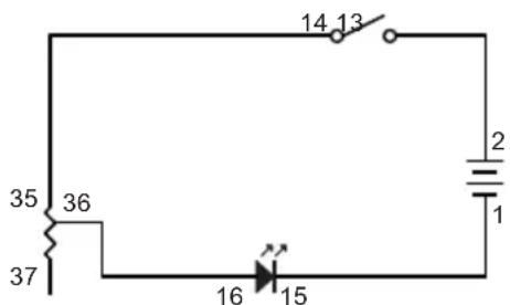
text_image
35 36 37 14 13 2 1 16 15- Complete all wiring connections as indicated in the sequence.
- Switch on the main switch.
- By adjusting the variable resistor, the amount of current in the circuit can be adjusted, and thus can alter the brightness of the LED.
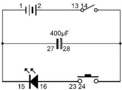
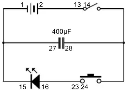
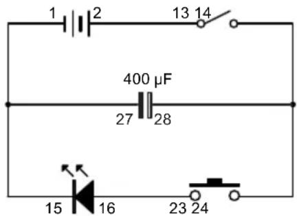
12.9 EXPERIMENT 9 - Demonstration of the function of the capacitor
Wiring Sequence
2-13, 14-28-24, 23-16, 15-27-1
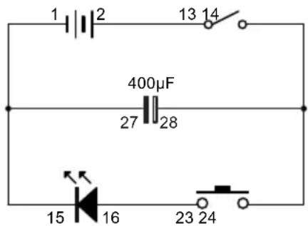
text_image
1 2 13 14 400µF 27 28 15 16 23 24User manual
- Complete all wiring connections as indicated in the sequence.
- Switch on the main switch. It appears that nothing happens. Actually the capacitor is being charged.
- After 1 to 2 seconds, switch off the main switch. The capacitor is charged and is storing a small amount of electricity.
- Press the push switch. The electricity stored in the capacitor will be released immediately and the LED will light up for a brief moment!
12.10 EXPERIMENT 10 - Diode and capacitor discharge
Wiring Sequence
2-14, 13-32-20, 19-18, 17-1-5-27, 28-31-23, 24-6
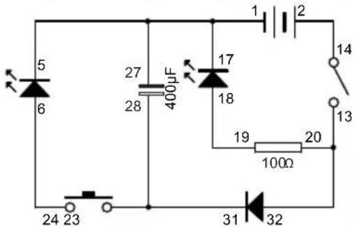
text_image
5 6 27 28 400µF 17 18 19 100Ω 20 14 13 24 23 31 32- Complete all wiring connections as indicated in the sequence.
- Switch on the main switch. The red LED will light up. Current flowing via the diode will charge the capacitor at the same time.
- When you press the push switch, the yellow LED will light up. Release the push switch so that the yellow LED will be turned off.
- Now switch off the main switch. The red LED will extinguish. If you press the push switch at this time, the yellow LED will light up for a brief moment due to the release of the stored electrical charge of the capacitor. However the red LED will not light up at all because the diode has blocked the current from the capacitor which is in an opposite direction.
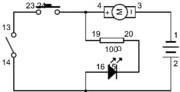
12.11 EXPERIMENT 11 - "AND Gate" circuit for LED
Wiring Sequence
2-24, 23-14, 13-16, 15-19, 20-4, 3-1
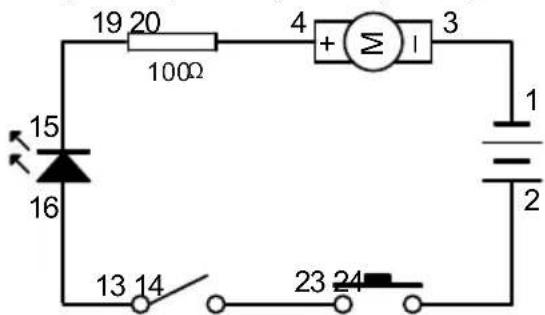
text_image
19 20 100Ω 4 + Σ I 3 15 16 1 2 13 14 23 24- Complete all wiring connections as indicated in the sequence.
- If you only switch on the main switch, or only press the push switch, the LED will not light up.
- If you switch on the main switch AND press the push switch together, then LED will light up.
- This is known as "AND Gate". Both switches have to be switched on in order to activate the LED.
| A AND B = C | ||
| A | B | C |
| 0 | 0 | 0 |
| 1 | 0 | 0 |
| 0 | 1 | 0 |
| 1 | 1 | 1 |
User manual
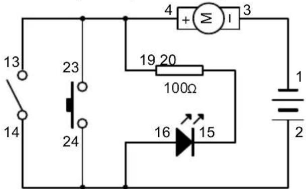
12.12 EXPERIMENT 12 - "OR Gate" circuit for LED
Wiring Sequence
2-24-14, 13-23-16, 15-19, 20-4, 3-1,
text_image
19 20 100Ω 4 + Σ I 3 15 16 23 24 13 14 1 2- Complete all wiring connections as indicated in the sequence.
- To light up the LED, you can either press the push switch OR switch on the main switch.
- This is known as "OR Gate". Switching on either switch OR switching on both switches will activate the LED.
| A OR B = C | ||
| A | B | C |
| 0 | 0 | 0 |
| 1 | 0 | 1 |
| 0 | 1 | 1 |
| 1 | 1 | 1 |
12.13 EXPERIMENT 13 - "NOT Gate" circuit for LED (with floating ball for extra excitement)
Wiring Sequence
2-14-16, 15-20, 19-13-4, 3-1
text_image
13 14 4 + Σ I 3 19 20 100Ω 16 15 1 2- Complete all wiring connections as indicated in the sequence.
- LED will automatically light up even though the main switch is off.
- When you switch on the main switch, LED will turn off.
- For the LED, this is known as "NOT Gate" - LED lights up when the switch is off. LED is off when switch is on.
- As an extra fun element, the blower will blow when the LED is off!
| NOT A = B | |
| A | B |
| 1 | 0 |
| 0 | 1 |
12.14 EXPERIMENT 14 - "NAND Gate" circuit for LED (with floating ball for extra excitement)
Wiring Sequence
User manual
2-14-16, 15-20, 13-23, 24-19-4, 3-1
text_image
23 24 13 14 4 + M I 3 19 20 100Ω 16 15 1 2- Complete all wiring connections as indicated in the sequence.
- LED will automatically light up.
- LED will be turned off only when both push switch and main switch are switched on. This is called "NAND gate".
- "NAND gate" is the exact opposite of "AND gate".
- As an extra fun element, blower will blow when the LED is off!
| A NAND B = C | ||
| A | B | C |
| 0 | 0 | 1 |
| 1 | 0 | 1 |
| 0 | 1 | 1 |
| 1 | 1 | 0 |
12.15 EXPERIMENT 15 – “NOR Gate” circuit for LED (with floating ball for extra excitement)
Wiring Sequence
2-24-14-16, 15-20, 19-23-13-4, 3-1
text_image
13 14 23 24 4 + Σ 1 3 19 20 100Ω 16 15 1 2- Complete all wiring connections as indicated in the sequence.
- LED will automatically light up.
- When both the main switch and push switch are off, then LED will light up. When the main switch or push switch is/are on, LED will be off. This is known as "NOR Gate".
- "NOR Gate" is the exact opposite of "OR Gate".
- As an extra fun element, the blower will blow when the LED is off!
| A NOR B = C | ||
| A | B | C |
| 0 | 0 | 1 |
| 1 | 0 | 0 |
| 0 | 1 | 0 |
| 1 | 1 | 0 |
User manual
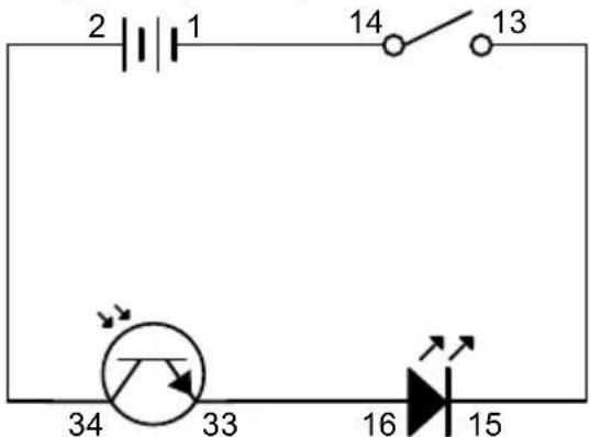
12.16 EXPERIMENT 16 - A simple demonstration of the light sensor
Wiring Sequence
2-34, 33-16, 15-13, 14-1
text_image
2 1 14 13 34 33 16 15- Complete all wiring connections as indicated in the sequence.
- Switch on the main switch. You may notice that the LED lights up very dimly. This indicates only a very small amount of current is flowing through it. It depends on the intensity of light falling onto the light sensor. If you perform this experiment in a darker place, the LED may not light up at all.
- If you use a torch to shine on the light sensor, you can see that the LED light up brightly. This is because when there is more light, more current will be able to pass through the light sensor and light up the LED.
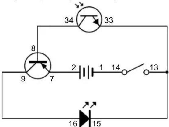
12.17 EXPERIMENT 17 – A simple demonstration of a function of the PNP transistor
Wiring Sequence
2-7, 9-16, 8-34, 33-15-13, 14-1
text_image
34 33 8 9 7 2 1 14 13 16 15- Complete all wiring connections as indicated in the sequence.
- Switch on the main switch. This time, even with a small amount of light, the LED will light up brightly!
- It is because in this circuit, the PNP transistor is the real gateway to the LED, and the light sensor is only acting as a switch for opening the gateway! When the upper part of the circuit is not connected, no current is flowing through the "Emitter" to the "Base" of the transistor. So the gateway of the "Emitter" to the "Collector" is shut. When light falls on the light sensor, the upper circuit is connected; a very small amount of current passes through the "Emitter" to the "Base", and then the gateway of the "Emitter" to the "Collector" is opened! Electric current from the battery can then flow through the transistor to the LED, and therefore the LED will light up brightly! This circuit makes the light sensor to become a sensitive switch to detect light.
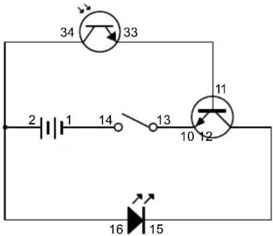
12.18 EXPERIMENT 18 - A simple demonstration of a function of the NPN transistor
Wiring Sequence
2-34-16, 15-12, 11-33, 10-13, 14-1
User manual
text_image
34 33 2 1 14 13 10 12 11 16 15- Complete all wiring connections as indicated in the sequence.
- Switch on the main switch. Again, this time even with a small amount of light, the LED will light up brightly!
- This is pretty much the same as the case of the PNP transistor. It is just the polarities of the transistor that are reversed.
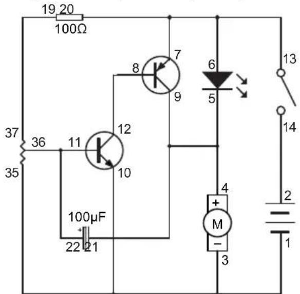
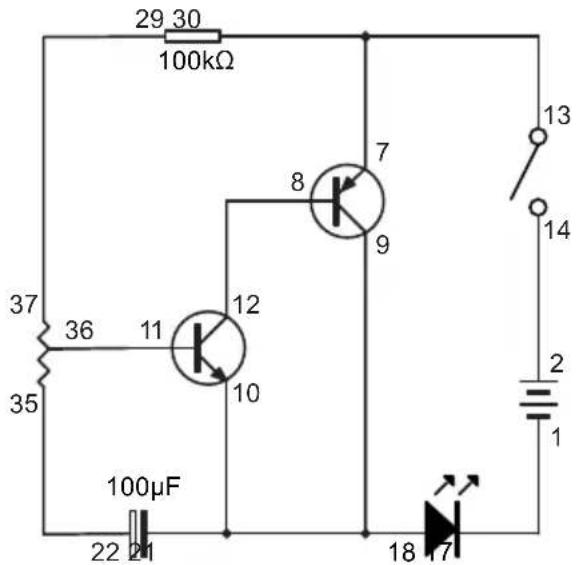
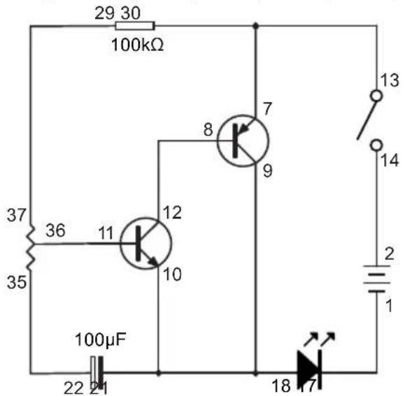
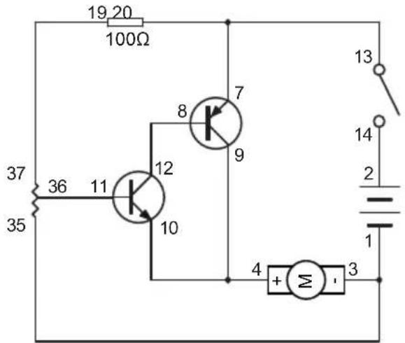
12.19 EXPERIMENT 19 - Delayed lighting up LED
Wiring Sequence
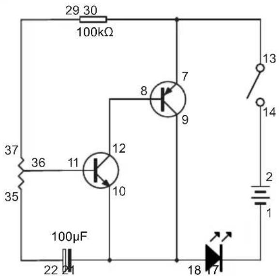
2-14, 13-7-30, 8-12, 29-37, 11-36, 35-22, 18-10-21-9, 17-1

text_image
29 30 100kΩ 37 36 11 12 8 7 35 10 9 100μF 22 21 18 17 13 14 2 1- Complete all wiring connections as indicated in the sequence.
- Switch on the main switch. Because of the capacitor, the LED will not light up immediately. The LED will light up after a while.
NOTE: If the experiment does not work, you may need to "discharge" the capacitor first. To "discharge", connect any wire to 21-22 for a second. This way the electricity stored in the capacitor will be "discharged" and then the experiment can work again.
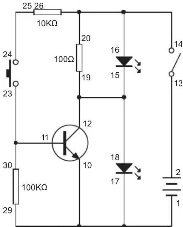
12.20 EXPERIMENT 20 - Delayed extinguishing LED
Wiring Sequence
2-14, 13-7-30-24, 23-22-25, 26-11, 12-29-8, 9-6, 5-10-21-1
User manual

text_image
24 23 10kΩ 25 26 22 100μF 30 100kΩ 29 8 7 9 12 11 10 6 5 13 14 2 1- Complete all wiring connections as indicated in the sequence.
- Switch on the main switch.
- By pressing the push switch, LED will light up.
- After you have released the push switch, just wait for some time and see. The LED will gradually extinguish.
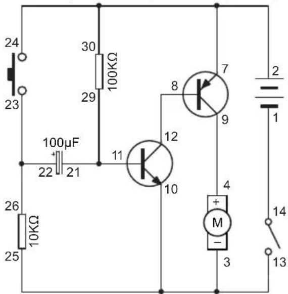
12.21 EXPERIMENT 21 - Light control blower (Light type)
Wiring Sequence
2-7-34, 33-30-11, 12-8, 9-4, 3-10-29-13, 14-1
text_image
34 33 100kΩ 30 29 11 10 8 7 9 4 + M - 3 2 1 14 13- Complete all wiring connections as indicated in the sequence.
- Switch on the main switch. The blower will blow.
- Cover the light sensor, and the blower will become weaker or even stop operating. Uncover it to resume operation.
12.22 EXPERIMENT 22 - Light control blower (Dark type)
Wiring Sequence
2-7-30, 29-34-11, 12-8, 9-4, 3-10-33-13, 14-1
User manual

text_image
30 100kΩ 29 8 7 9 11 12 10 4 + M - 3 2 1 14 13 34 33- Complete all wiring connections as indicated in the sequence.
- Switch on the main switch. Cover the light sensor and the blower will blow.
- Uncover the light sensor, and the blower will become weaker or even stop operating.
12.23 EXPERIMENT 23 - Alternating LED and blower
Wiring Sequence
2-14, 13-6-7-20, 5-4-9-21, 8-12, 11-36-22, 1-3-35-10, 19-37
text_image
19 20 100Ω 37 36 11 12 35 10 100μF 22 21 8 7 9 6 5 4 + M - 3 13 14 2 1- Complete all wiring connections as indicated in the sequence.
- Switch on the main switch and try to adjust the variable resistor slowly.
- Both LED and blower will be activated alternately.
- The alternate frequency for both devices depends on the set value of the variable resistor.
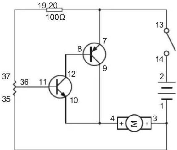
12.24 EXPERIMENT 24 - Speed adjustable blower
Wiring Sequence
2-14, 13-7-20, 8-12, 19-37, 11-36, 35-3-1, 4-10-9
User manual
text_image
19 20 100Ω 37 36 11 12 8 7 35 10 9 4 + Σ - 3 13 14 2 1- Complete all wiring connections as indicated in the sequence.
- Switch on the main switch.
- By adjusting the variable resistor, you can adjust the blowing power of the blower.
12.25 EXPERIMENT 25 - Connection indicator
Wiring Sequence
2-13, 14-16-20-26, 25-24, 15-18-19-12, 23-11-30, 29-10-17-1
text_image
25 26 10KΩ 24 23 100Ω 20 19 16 15 14 13 12 11 10 30 100KΩ 29 18 17 2 1- Complete all wiring connections as indicated in the sequence.
- Switch on the main switch. Red LED will light up but blue LED will not.
- Press the push switch. Blue LED will light up and red LED will extinguish.
- Release the push switch. Red LED will light up again and blue LED will extinguish.
- This principle can be used for indicating the break/connect of circuit: When the door, car-door or window is closed, it is just like the push switch is being pressed, and thus blue LED lights up while red LED does not. When the door, car-door or window is opened, this is just like the push switch is released, and thus red LED lights up while blue LED goes off.
User manual
12.26 EXPERIMENT 26 - Manual control stop-and-resume blower
Wiring Sequence
2-7-30-24, 23-26-22, 21-29-11, 12-8, 9-4, 3-10-25-13, 14-1
text_image
24 23 100μF 22 21 30 100KΩ 29 11 12 10 8 7 9 4 + M - 3 2 1 14 13 26 10KΩ 25- Complete all wiring connections as indicated in the sequence.
- Switch on the main switch. After a while the blower will blow.
- Press the push switch, and the blowing speed will be changed for a while. Do not release the push switch, and the speed will gradually back to the original blowing speed.
- And then release the push switch. The blower will stop for a while. After waiting for some time, the blower will resume operation again like it did at the beginning of the experiment!
© COPYRIGHT NOTICE
The copyright to this manual is owned by Velleman nv. All worldwide rights reserved. No part of this manual may be copied, reproduced, translated or reduced any electronic medium or otherwise without the prior written consent of the copyright holder.
HANDLEIDING
1. Inleiding
natural_image
Close-up of a black cylindrical capacitor with two metallic pins (no visible text or symbols)
text_image
+| -Elektrolytische condensator Schakelsymbool
natural_image
Close-up of four black integrated circuit chips with metallic pins, arranged on a plain background (no text or symbols visible)text_image
anode Cathodenatural_image
Pure electrical circuit lines without any symbolsSchakelsymbool
text_image
1st Digit 2nd Digit Multiplier Tolerancenatural_image
Close-up of two black electronic components with metallic leads (no visible text or symbols)Transistor
NPN

PNP
Schakelsymbool
text_image
Diagram illustrating three steps of a device assembly or cleaning process, labeled 01, 02, and 03 with directional arrows and component illustrations.
text_image
Diagram of a device rear panel with labeled components including transistors, main switch, and light sensor, plus wiring connections.User manual
12. Experimenten
12.1 EXPERIMENT 1 - Blower (Zwevende bal)
Bedradingsvolgorde
2-14, 13-4, 1-3

text_image
4 + Σ I 3 1 2 13 142-13, 14-28-24, 23-16, 15-27-1
User manual

text_image
1 2 13 14 400μF 27 28 15 16 23 242-14, 13-7-30, 8-12, 29-37, 11-36, 35-22, -10-2118-9, 17-1

text_image
29 30 100kΩ 37 36 11 12 8 7 35 10 9 100μF 22 21 18 17 13 14 2 12-14, 13-7-20, 8-12, 19-37, 11-36, -3-153, 4-10-9
User manual

text_image
19 20 100Ω 37 36 11 12 8 7 35 10 9 4 + Σ - 3 13 14 2 1natural_image
Close-up of a black cylindrical capacitor with two metallic leads (no visible text or symbols)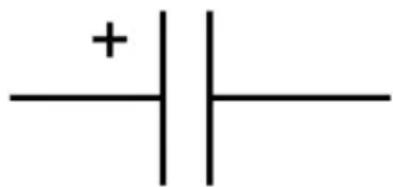
text_image
+| -natural_image
Close-up of four black integrated circuit chips with metallic pins, arranged on a plain background (no text or symbols visible)Circuit intégré
User manual
text_image
anode Cathodenatural_image
Pure electrical circuit lines without any symbolsSymbole du circuit
User manual
text_image
1st Digit 2nd Digit Multiplier Tolerance| Couleur 1er | 2ème | 3rd - multiplicateur | Tolérance | |
| Noir | 0 | 0 | x 1 | |
| Marron | 1 | 1 | x 10 | |
| Rouge | 2 | 2 | x 100 | |
| Orange | 3 | 3 | x 1000 | |
| Jaune | 4 | 4 | x 10000 | |
| Vert | 5 | 5 | x 100000 | |
| Bleu | 6 | 6 | x 1000000 | |
| Pourpre | 7 | 7 | ||
| Gris | 8 | 8 | ||
| Blanc | 9 | 9 | ||
| Marron | +/- 1% | |||
| Rouge | +/- 2% | |||
| L'or | x 0.1 | +/- 5% | ||
| Argent | x 0.01 | +/- 10% |
natural_image
Close-up of two black electronic components with metallic leads (no visible text or symbols)Transistor
NPN
PNP
Symbole du
circuit
User manual
text_image
Diagram illustrating three steps of a device assembly or installation, labeled 01, 02, and 03 with directional arrows and component illustrations.
text_image
Diagram of a device rear panel with labeled components including transistors, main switch, and light sensor, plus wiring connections.User manual
12. Expériences
12.1 EXPÉRIMENTATION 1 - Soufflerie (balle flottante)
Séquence de câblage
2-14, 13-4, 1-3
text_image
4 + Σ 1 3 1 2 13 142-13, 14-28-24, 23-16, 15-27-1
User manual
text_image
1 2 13 14 400µF 27 28 15 16 23 24| A OU B = C | ||
| A | B | C |
| 0 | 0 | 0 |
| 1 | 0 | 1 |
| 0 | 1 | 1 |
| 1 | 1 | 1 |
User manual
| PAS A = B | |
| A | B |
| 1 | 0 |
| 0 | 1 |
2-14, 13-7-30, 8-12, 29-37, 11-36, 35-22, -10-2118-9, 17-1
text_image
29 30 100kΩ 37 36 11 12 8 7 35 10 9 100μF 22 21 18 17 13 14 2 12-14, 13-7-20, 8-12, 19-37, 11-36, -3-153, 4-10-9
text_image
19 20 100Ω 37 36 11 12 8 7 35 10 9 4 + Σ 3 13 14 2 1natural_image
Pure electrical circuit symbol for a capacitor, no text or labels presentCondensador electrolítico Símbolo del circuito
natural_image
Close-up of four black integrated circuit chips with metallic pins, arranged on a white background (no text or symbols visible)natural_image
Pure electrical circuit lines without any symbolstext_image
1st Digit 2nd Digit Multiplier Tolerance| Color 1° 2a | 3rd - multiplicador | Tolerancia | ||
| Negro | 0 | 0 | x 1 | |
| Marrón | 1 | 1 | x 10 | |
| Rojo | 2 | 2 | x 100 | |
| Naranja | 3 | 3 | x 1000 | |
| Amarillo | 4 | 4 | x 10000 | |
| Verde | 5 | 5 | x 100000 | |
| Azul | 6 | 6 | x 1000000 | |
| Morado | 7 | 7 | ||
| Gris | 8 | 8 | ||
| Blanco | 9 | 9 | ||
| Marrón | +/- 1% | |||
| Rojo | +/- 2% | |||
| Oro | x 0.1 | +/- 5% | ||
| Plata | x 0.01 | +/- 10% | ||
natural_image
Close-up of two black electronic components with metallic leads (no visible text or symbols)Transistor

NPN
PNP
Símbolo del
circuito
text_image
Diagram showing three steps of a device assembly with labeled components and directional arrows indicating motion.
text_image
Diagram of a device rear panel with labeled components including transistors, main switch, and light sensor, plus wiring connections.User manual
12. Experimentos
12.1 EXPERIMENTO 1 - Soplador (Bola flotante)
2-13, 14-28-24, 23-16, 15-27-1

text_image
1 2 13 14 400 μF 27 28 15 16 23 24| A Y B = C | ||
| A | B | C |
| 0 | 0 | 0 |
| 1 | 0 | 0 |
| 0 | 1 | 0 |
| 1 | 1 | 1 |
2-14, 13-7-30, 8-12, 29-37, 11-36, 35-22, -10-2118-9, 17-1

text_image
29 30 100kΩ 37 36 11 12 8 7 35 10 9 100μF 22 21 18 17 13 14 2 12-14, 13-7-20, 8-12, 19-37, 11-36, -3-153, 4-10-9

text_image
19.20 100Ω 37 36 11 12 8 7 35 10 9 4 + Σ 3 13 14 2 1natural_image
Close-up of a black cylindrical capacitor with two metallic pins (no visible text or symbols)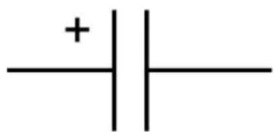
text_image
+| -natural_image
Close-up of several black integrated circuit chips with metallic pins, arranged in a row (no visible text or markings)text_image
anode Cathodenatural_image
Pure electrical circuit symbol diagram without any text or labelsSchaltkreissymbol
User manual
text_image
1st Digit 2nd Digit Multiplier Tolerance| Farbe 1. 2. | 3^rd - Multiplikator | Toleranz | ||
| Schwarz | 0 | 0 | x 1 | |
| Braun | 1 | 1 | x 10 | |
| Rot | 2 | 2 | x 100 | |
| Orange | 3 | 3 | x 1000 | |
| Gelb | 4 | 4 | x 10000 | |
| Grün | 5 | 5 | x 100000 | |
| Blau | 6 | 6 | x 1000000 | |
| Lila | 7 | 7 | ||
| Grau | 8 | 8 | ||
| Weiß | 9 | 9 | ||
| Braun | +/- 1% | |||
| Rot | +/- 2% | |||
| Gold | x 0.1 | +/- 5% | ||
| Silber | x 0.01 | +/- 10% |
natural_image
Close-up of two black electronic components with metallic leads (no visible text or symbols)Symbol
Transistor

NPN
PNP
Schaltkreis-
User manual
text_image
Diagram illustrating three steps of a device assembly or cleaning process, labeled 01, 02, and 03 with directional arrows and component illustrations.
text_image
Diagram of a device rear panel with labeled components including transistors, main switch, and light sensor, plus wiring connections.User manual
12. Experimente
2-13, 14-28-24, 23-16, 15-27-1

text_image
1 2 13 14 400 µF 27 28 15 16 23 242-14, 13-7-30, 8-12, 29-37, 11-36, 35-22, -10-2118-9, 17-1
User manual
text_image
29 30 100kΩ 37 36 11 12 8 7 35 10 9 100μF 22 21 18 17 13 14 2 12-14, 13-7-20, 8-12, 19-37, 11-36, -3-153, 4-10-9
text_image
19 20 100Ω 37 36 11 12 8 7 35 10 9 4 + Σ 3 13 14 2 1natural_image
Close-up of a black cylindrical capacitor with two metallic leads (no visible text or symbols)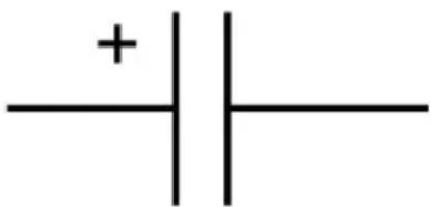
text_image
+| -natural_image
Close-up of several black integrated circuit chips with metallic pins, arranged in a row (no visible text or markings)Układ scalony
User manual
text_image
anode CathodeSymbol obwodu
natural_image
Pure electrical circuit lines without any symbolsSymbol obwodu
User manual
text_image
1st Digit 2nd Digit Multiplier Tolerancenatural_image
Close-up of two black electronic components with metallic leads (no visible text or symbols)Tranzystor
NPN

PNP
Symbol obwodu
text_image
Diagram illustrating three steps of a device assembly or cleaning process, labeled 01, 02, and 03 with directional arrows and component illustrations.
text_image
Diagram of a device rear panel with labeled components including transistors, main switch, and light sensor, plus wiring connections.User manual
12. Eksperymenty
2-13, 14-28-24, 23-16, 15-27-1
text_image
1 2 13 14 400µF 27 28 15 16 23 24| A AND B = C | ||
| A | B | C |
| 0 | 0 | 0 |
| 1 | 0 | 0 |
| 0 | 1 | 0 |
| 1 | 1 | 1 |
| NIE A = B | |
| A | B |
| 1 | 0 |
| 0 | 1 |
2-14, 13-7-30, 8-12, 29-37, 11-36, 35-22, -10-2118-9, 17-1

text_image
29 30 100kΩ 37 36 11 12 8 7 35 10 9 100μF 22 21 18 17 13 14 2 12-14, 13-7-20, 8-12, 19-37, 11-36, -3-153, 4-10-9

text_image
19 20 100Ω 37 36 11 12 8 7 35 10 9 4 + Σ 3 13 14 2 1natural_image
Close-up of four black integrated circuit chips with metallic pins, arranged in a row (no visible text or markings)Circuito integrado
natural_image
Pure electrical circuit symbol for a transistor, without any text or labelsSímbolo do circuito
User manual
text_image
1st Digit 2nd Digit Multiplier Tolerancenatural_image
Close-up of three black electronic components with metallic leads (no visible text or symbols)Transístor

NPN

PNP
Símbolo do
circuito
text_image
Diagram showing three steps of a device assembly with labeled components and directional arrows indicating motion.
text_image
Diagram of a device rear panel with labeled components including transistors, main switch, and light sensor, plus wiring connections.User manual
12. Experiências
2-13, 14-28-24, 23-16, 15-27-1

text_image
1 2 13 14 400 μF 27 28 15 16 23 24| A E B = C | ||
| A | B | C |
| 0 | 0 | 0 |
| 1 | 0 | 0 |
| 0 | 1 | 0 |
| 1 | 1 | 1 |
| A OU B = C | ||
| A | B | C |
| 0 | 0 | 0 |
| 1 | 0 | 1 |
| 0 | 1 | 1 |
| 1 | 1 | 1 |
User manual
2-14, 13-7-30, 8-12, 29-37, 11-36, 35-22, -10-2118-9, 17-1
text_image
29 30 100kΩ 37 36 11 12 8 7 35 10 9 100μF 22 21 18 17 13 14 2 12-14, 13-7-20, 8-12, 19-37, 11-36, -3-153, 4-10-9

text_image
19.20 100Ω 37 36 11 12 8 7 35 10 9 4 + Σ 3 13 14 2 1natural_image
Close-up of four black integrated circuit chips with metallic pins, arranged on a white background (no text or symbols visible)Circuito integrato
User manual
text_image
anode Cathodenatural_image
Pure electrical circuit lines without any symbolstext_image
1st Digit 2nd Digit Multiplier Tolerance| Colore 1a | 2a | 3^rd - moltiplicatore | Tolleranza | |
| Nero | 0 | 0 | x 1 | |
| Marrone | 1 | 1 | x 10 | |
| Rosso | 2 | 2 | x 100 | |
| Arancione | 3 | 3 | x 1000 | |
| Giallo | 4 | 4 | x 10000 | |
| Verde | 5 | 5 | x 100000 | |
| Blu | 6 | 6 | x 1000000 | |
| Viola | 7 | 7 | ||
| Grigio | 8 | 8 | ||
| Bianco | 9 | 9 | ||
| Marrone | +/- 1% | |||
| Rosso | +/- 2% | |||
| Oro | x 0.1 | +/- 5% | ||
| Argento | x 0.01 | +/- 10% |
natural_image
Close-up of three black electronic components with metallic leads (no visible text or symbols)Transistor
NPN

PNP
Simbolo del
circuito
text_image
Diagram showing three steps of a device assembly with labeled components and directional arrows indicating process flow.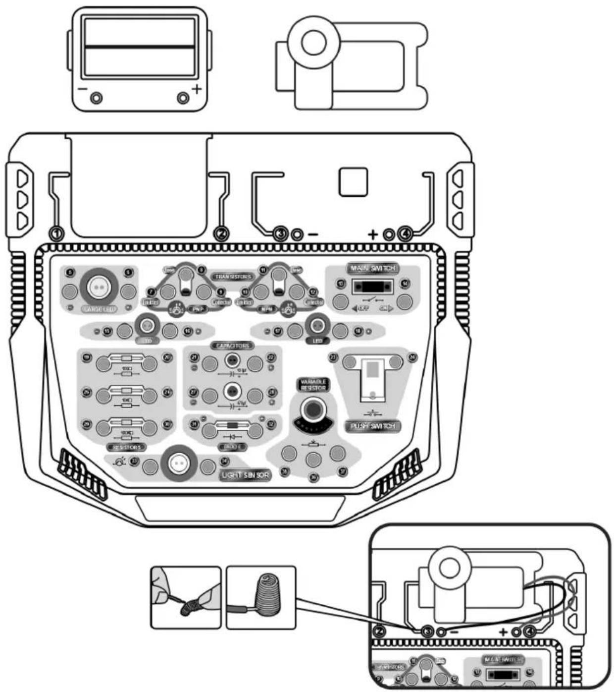
text_image
Diagram of a device rear panel with labeled components including transistors, LED, and switch controlsUser manual
12. Esperimenti
2-13, 14-28-24, 23-16, 15-27-1
text_image
1 2 13 14 400 μF 27 28 15 16 23 24| A E B = C | ||
| A | B | C |
| 0 | 0 | 0 |
| 1 | 0 | 0 |
| 0 | 1 | 0 |
| 1 | 1 | 1 |
2-14, 13-7-30, 8-12, 29-37, 11-36, 35-22, -10-2118-9, 17-1

text_image
29 30 100kΩ 37 36 11 12 8 7 35 10 9 100μF 22 21 18 17 13 14 2 12-14, 13-7-20, 8-12, 19-37, 11-36, -3-153, 4-10-9
text_image
19.20 100Ω 37 36 11 12 8 7 35 10 9 4 + Σ 3 13 14 2 1Velleman® Service and Quality Warranty
Since its foundation in 1972, Velleman® acquired extensive experience in the electronics world and currently distributes its products in over 85 countries. All our products fulfil strict quality requirements and legal stipulations in the EU. In order to ensure the quality, our products regularly go through an extra quality check, both by an internal quality department and by specialized external organisations. If, all precautionary measures notwithstanding, problems should occur, please make appeal to our warranty (see guarantee conditions).
General Warranty Conditions Concerning Consumer Products (for EU):
- All consumer products are subject to a 24-month warranty on production flaws and defective material as from the original date of purchase.
- Velleman® can decide to replace an article with an equivalent article, or to refund the retail value totally or partially when the complaint is valid and a free repair or replacement of the article is impossible, or if the expenses are out of proportion.
You will be delivered a replacing article or a refund at the value of 100% of the purchase price in case of a flaw occurred in the first year after the date of purchase and delivery, or a replacing article at 50% of the purchase price or a refund at the value of 50% of the retail value in case of a flaw occurred in the second year after the date of purchase and delivery.
- Not covered by warranty:
- all direct or indirect damage caused after delivery to the article (e.g. by oxidation, shocks, falls, dust, dirt, humidity...), and by the article, as well as its contents (e.g. data loss), compensation for loss of profits;
- consumable goods, parts or accessories that are subject to an aging process during normal use, such as batteries (rechargeable, non-rechargeable, built-in or replaceable), lamps, rubber parts, drive belts... (unlimited list);
- flaws resulting from fire, water damage, lightning, accident, natural disaster, etc....:
- flaws caused deliberately, negligently or resulting from improper handling, negligent maintenance, abusive use or use contrary to the manufacturer's instructions;
- damage caused by a commercial, professional or collective use of the article (the warranty validity will be reduced to six (6) months when the article is used professionally):
- damage resulting from an inappropriate packing and shipping of the article; - all damage caused by modification, repair or alteration performed by a third party without written permission by Velleman®.
- Articles to be repaired must be delivered to your Velleman® dealer, solidly packed (preferably in the original packaging), and be completed with the original receipt of purchase and a clear flaw description.
- Hint: In order to save on cost and time, please reread the manual and check if the flaw is caused by obvious causes prior to presenting the article for repair. Note that returning a non-defective article can also involve handling costs.
- Repairs occurring after warranty expiration are subject to shipping costs. - The above conditions are without prejudice to all commercial warranties.
The above enumeration is subject to modification according to the article (see article's manual).