MS-7582 G52-75821X2 - Motherboard MSI - Free user manual and instructions
Find the device manual for free MS-7582 G52-75821X2 MSI in PDF.
Download the instructions for your Motherboard in PDF format for free! Find your manual MS-7582 G52-75821X2 - MSI and take your electronic device back in hand. On this page are published all the documents necessary for the use of your device. MS-7582 G52-75821X2 by MSI.
USER MANUAL MS-7582 G52-75821X2 MSI
G52-75821X2 ▍ Preface Copyright Notice The material in this document is the intellectual property of MICRO-STAR INTERNATIONAL. We take every care in the preparation of this document, but no guarantee is given as to the correctness of its contents. Our products are under continual improvement and we reserve the right to make changes without notice. Trademarks All trademarks are the properties of their respective owners.
MSI® is registered trademark of Micro-Star Int’l Co.,Ltd. NVIDIA® is registered trademark of NVIDIA Corporation. ATI® is registered trademark of ATI Technologies, Inc. AMD® is registered trademarks of AMD Corporation. Intel® is registered trademarks of Intel Corporation. Windows® is registered trademarks of Microsoft Corporation. AMI® is registered trademark of American Megatrends, Inc. Award® is a registered trademark of Phoenix Technologies Ltd. Sound Blaster® is registered trademark of Creative Technology Ltd. Realtek® is registered trademark of Realtek Semiconductor Corporation. JMicron® is registered trademark of JMicron Technology Corporation. Netware® is a registered trademark of Novell, Inc. Revision History Revision Revision History Date V1.0 First release for Europe November 2009 Technical Support If a problem arises with your system and no solution can be obtained from the user’s manual, please contact your place of purchase or local distributor. Alternatively, please try the following help resources for further guidance.
Always read the safety instructions carefully. Keep this User’s Manual for future reference. Keep this equipment away from humidity. Lay this equipment on a reliable flat surface before setting it up. The openings on the enclosure are for air convection hence protects the equipment from overheating. DO NOT COVER THE OPENINGS. ■ Make sure the voltage of the power source and adjust properly 110/220V before connecting the equipment to the power inlet. ■ Place the power cord such a way that people can not step on it. Do not place anything over the power cord. ■ Always Unplug the Power Cord before inserting any add-on card or module. ■ All cautions and warnings on the equipment should be noted. ■ Never pour any liquid into the opening that could damage or cause electrical shock. ■ If any of the following situations arises, get the equipment checked by service personnel:
The power cord or plug is damaged.
Liquid has penetrated into the equipment.
The equipment has been exposed to moisture.
The equipment does not work well or you can not get it work according to User’s Manual.
The equipment has dropped and damaged.
The equipment has obvious sign of breakage. DO NOT LEAVE THIS EQUIPMENT IN AN ENVIRONMENT UNCONDITIONED, STORAGE TEMPERATURE ABOVE 600 C (1400F), IT MAY DAMAGE THE EQUIPMENT. CAUTION: Danger of explosion if battery is incorrectly replaced. Replace only with the same or equivalent type recommended by the manufacturer. 這是甲類資訊產品,在居住的環境中使用時,可能會造成無線電干擾,在這種情況下, 使用者會被要求採取某些適當的對策。 For better environmental protection, waste batteries should be collected separately for recycling special disposal. iii ▍ Preface FCC-B Radio Frequency Interference Statement This equipment has been tested and found to comply with the limits for a Class B digital device, pursuant to Part 15 of the FCC Rules. These limits are designed to provide reasonable protection against harmful interference in a residential installation. This equipment generates, uses and can radiate radio frequency energy and, if not installed and used in accordance with the instructions, may cause harmful interference to radio communications. However, there is no guarantee that interference will not occur in a particular installation. If this equipment does cause harmful interference to radio or television reception, which can be determined by turning the equipment off and on, the user is encouraged to try to correct the interference by one or more of the measures listed below.
Reorient or relocate the receiving antenna.
Increase the separation between the equipment and receiver.
Connect the equipment into an outlet on a circuit different from that to which the receiver is connected.
Consult the dealer or an experienced radio/television technician for help. Notice 1 The changes or modifications not expressly approved by the party responsible for compliance could void the user’s authority to operate the equipment. Notice 2 Shielded interface cables and A.C. power cord, if any, must be used in order to comply with the emission limits. VOIR LA NOTICE D’INSTALLATION AVANT DE RACCORDER AU RESEAU. Micro-Star International MS-7582 This device complies with Part 15 of the FCC Rules. Operation is subject to the following two conditions:
1) this device may not cause harmful interference, and
2) this device must accept any interference received, including interference that may
cause undesired operation.
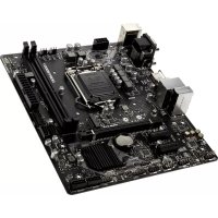
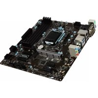
FUZION Series English Europe version ▍ MS-7582 Mainboard Mainboard Specifications Processor Support ■ Intel® Core™ i7 and Core™ i5 (Lynnfield & Clarkdale) processor in the LGA1156 package (For the latest information about CPU, please visit http://www.msi.com/index. php?func=cpuform2) Base Clock ■ 133 MHz Chipset ■ Intel® P55 / Lucid® Hydra 200 chipset Memory Support ■ 4 DDR3 DIMMs support DDR3 2133 *(OC)/ 2000 *(OC)/ 1800 *(OC)/1600 *(OC)/ 1333/ 1066 DRAM (16GB Max) ■ Supports Dual-Channel mode *(For more information on compatible components, please visit http://www.msi.com/index.php?func=testreport) LAN ■ Supports Dual LAN (10/100/1000) by Realtek® RTL8111DL IEEE 1394 ■ Chip integrated by VIA® VT6315N ■ Transfer rate is up to 400Mbps Audio ■ QuantumWaveTM Audio Card ■ Creative EAX® ADVANCED HD 5.0 ■ THX TruStudio PCTM ■ Creative ALchemy ■ 7.1 Channel High Definition Audio Codec with jack sensing ■ Realtek® ALC889 ■ Compliant with Azalia 1.0 Spec ■ Supports1x S/PDIF out header ■ Supports Coaxial/Optical S/PDIF out ports on rear IDE ■ 1 IDE port by JMicron® JMB363 ■ Supports Ultra DMA 66/100/133 mode ■ Supports PIO, Bus Master operation mode SATA ■ 6 SATAII (SATA1~6) ports by Intel® P55 ■ 4 SATAII (SATA7/ 8/ 9/ 10) ports by two JMicron® JMB322 ■ 2 ESATA/ USB Combo port (back panel) by JMicron® JMB362 ■ Supports storage and data transfers at up to 3 Gb/s En-2 English RAID ■ SATA1~6 support Intel® Matrix Storage Technology (AHCI/ RAID 0/ 1/ 5/ 10) by Intel® P55 Hardware RAID ■ SATA7 & SATA8 support RAID 0/ 1 & JBOD mode by 1st JMicron® JMB322 ■ SATA9 & SATA10 support RAID 0/ 1 & JBOD mode by 2nd JMicron® JMB322 Connectors ■ Back panel - 1 PS/2 keyboard port - 1 PS/2 mouse port - 1 D-LED3 panel connector (optional) - 8 USB 2.0 ports - 1 IEEE 1394 port - 2 ESATA/ USB Combo port - 2 LAN ports ■ On-Board - 2 USB 2.0 connectors - 1 IEEE 1394 connector - 1 Chassis Intrusion connector - 1 TPM Module connector (optional) - 1 Green Power Genie connector (optional) - 1 Over-Voltage switch & 1 set voltage check point - 1 Power button - 1 Reset button - 1 Green Power button - 1 Clear CMOS button - 1 OC Genie button - 1 CPU Phase LED panel Slots ■ 3 PCI Express 2.0 x16 slots - PCI_E2/ PCI_E4/ PCI_E5 will be x16/ x16/ x0 or x16/ x8/ x8 ■ 2 PCI Express 2.0 x1 slots - Only PCI_E1 supports installing the Realtek® Audio card ■ 2 PCI 2.2 slots, support 3.3V/ 5V PCI bus Interface Form Factor ■ ATX (30.5cm X 24.4 cm) Mounting ■ 9 mounting holes If you need to purchase accessories and request the part numbers, you could search the product web page and find details on our web address below http://www.msi.com/index.php En-3 ▍ MS-7582 Mainboard Quick Components Guide CPU, En-5 SYSFAN3, En-15 CPUFAN, En-15 JPWR2, En-11 DDR3, En-9 SYSFAN2, En-15 JPWR1, En-11 JSMB1, En-18 Back Panel, En-12 V-Check Point, En-22 V Switch, En-21 SYSFAN1, En-15 PCIE, En-23 SATA, En-14 IDE1, En-13 SYSFAN4, En-15 PCI, En-26 JFP1/ JFP2, En-16 JTPM1, En-18 Green Power/ Reset/ Power, En-20 CLR_CMOS1, En-19 JCI1, En-14 OC_Genie, En-19 J1394_1, En-16 En-4 JUSB1~2, En-17 English CPU (Central Processing Unit) When you are installing the CPU, make sure to install the cooler to prevent overheating. If you do not have the CPU cooler, consult your dealer before turning on the computer. For the latest information about CPU, please visit http://www.msi.com/index. php?func=cpuform2 Important Overheating Overheating will seriously damage the CPU and system. Always make sure the cooling fan can work properly to protect the CPU from overheating. Make sure that you apply an even layer of thermal paste (or thermal tape) between the CPU and the heatsink to enhance heat dissipation. Replacing the CPU While replacing the CPU, always turn off the ATX power supply or unplug the power supply’s power cord from the grounded outlet first to ensure the safety of CPU. Overclocking This mainboard is designed to support overclocking. However, please make sure your components are able to tolerate such abnormal setting, while doing overclocking. Any attempt to operate beyond product specifications is not recommended. We do not guarantee the damages or risks caused by inadequate operation or beyond product specifications. Introduction to LGA 1156 CPU The pin-pad side of LGA 1156 CPU. Alignment Key Yellow triangle is the Pin 1 indicator The surface of LGA 1156 CPU. Remember to apply some thermal paste on it for better heat dispersion. Alignment Key Yellow triangle is the Pin 1 indicator En-5 ▍ MS-7582 Mainboard CPU & Cooler Installation When you are installing the CPU, make sure the CPU has a cooler attached on the top to prevent overheating. Meanwhile, do not forget to apply some thermal paste on CPU before installing the heat sink/cooler fan for better heat dispersion. Follow the steps below to install the CPU & cooler correctly. Wrong installation will cause the damage of your CPU & mainboard.
1. Open the load level.
2. Lift the load lever up to fully open
3. The CPU socket has a plastic cap on
it to protect the contact from damage. Before you install CPU, always cover it to protect the socket pin. Romove the cap (as the arrow shows).
4. After confirming the CPU direction for
correct mating, put down the CPU in the socket housing frame. Be sure to grasp on the edge of the CPU base. Note that the alignment keys are matched. Alignment Key En-6 English
5. Visually inspect if the CPU is seated
well into the socket. If not, take out the CPU with pure vertical motion and reinstall.
6. Engage the load lever while pressing
down lightly onto the load plate. Alignment Key
7. Secure the lever near the hook end
under the retention tab.
8. Make sure the four hooks are in porper position before you install the
- Confirm if your CPU cooler is firmly installed before turning on your system.
- Do not touch the CPU socket pins to avoid damaging. En-7 ▍ MS-7582 Mainboard
9. Align the holes on the mainboard with
the heatsink. Push down the cooler until its four clips get wedged into the holes of the mainboard.
10. Press the four hooks down to fasten
11. Turn over the mainboard to confirm
that the clip-ends are correctly inserted.
12. Finally, attach the CPU Fan cable to
the CPU fan connector on the mainboard. Mainboard Hook Important
- Read the CPU status in BIOS.
- Whenever CPU is not installed, always protect your CPU socket pin with the plastic cap covered (shown in Figure 1) to avoid damaging.
- Mainboard photos shown in this section are for demonstration of the CPU/ cooler installation only. The appearance of your mainboard may vary depending on the model you purchase.
- Please refer to the documentation in the CPU fan package for more details about the CPU fan installation. En-8 English Memory These DIMM slots are used for installing memory modules. For more information on compatible components, please visit http://www.msi.com/index.php?func=testreport DDR3 240-pin, 1.5V 48x2=96 pin 72x2=144 pin Memory Population Rule Please refer to the following illustrations for memory population rules. Dual-Channel mode Population Rule In Dual-Channel mode, the memory modules can transmit and receive data with two data bus lines simultaneously. Enabling Dual-Channel mode can enhance the system performance. The following illustrations explain the population rules for Dual-Channel mode.
DIMM3 Installed Empty Important
- DDR3 memory modules are not interchangeable with DDR2 and the DDR3 standard is not backwards compatible. You should always install DDR3 memory modules in the DDR3 DIMM slots.
- In Dual-Channel mode, make sure that you install memory modules of the same type and density in different channel DIMM slots.
- To enable successful system boot-up (Lynnfield CPU especially), always insert the memory modules into the DIMM1 first.
- Due to the chipset resource deployment, the system density will only be detected up to 15+GB (not full 16GB) when each DIMM is installed with a 4GB memory module. En-9 ▍ MS-7582 Mainboard Installing Memory Modules
1. The memory module has only one notch on the center and will only fit in the right
2. Insert the memory module vertically into the DIMM slot. Then push it in until the
golden finger on the memory module is deeply inserted in the DIMM slot. The plastic clip at each side of the DIMM slot will automatically close when the memory module is properly seated.
3. Manually check if the memory module has been locked in place by the DIMM slot
clips at the sides. Notch Volt Important You can barely see the golden finger if the memory module is properly inserted in the DIMM slot. En-10 English Power Supply ATX 24-pin Power Connector: JPWR1 This connector allows you to connect an ATX 24-pin power supply. To connect the ATX 24-pin power supply, make sure the plug of the power supply is inserted in the proper orientation and the pins are aligned. Then push down the power supply firmly into the connector. You may use the 20-pin ATX power supply as you like. If you’d like to use the 20-pin ATX power supply, please plug your power supply along with pin 1 & pin 13.
ATX 8-pin Power Connector: JPWR2 This connector is used to provide 12V power output to the CPU.
- Make sure that all the connectors are connected to proper ATX power supplies to ensure stable operation of the mainboard.
- Power supply of 400 watts (and above) is highly recommended for system stability.
- ATX 12V power connection should be greater than 18A. En-11 ▍ MS-7582 Mainboard Back Panel LAN LAN USB Port USB Port 1394 Port Mouse USB Port D-LED3 panel connector (optional) Keyboard ESATA/ USB Combo Port USB Port ESATA/ USB USB Port Combo Port ▶ Mouse/Keyboard The standard PS/2® mouse/keyboard DIN connector is for a PS/2® mouse/keyboard. ▶ USB Port The USB (Universal Serial Bus) port is for attaching USB devices such as keyboard, mouse, or other USB-compatible devices. ▶ D-LED3 Panel Connector (optional) This connector connects to a D-LED3 (Debug-LED3) panel (optional), which shows information on the panel for you and identify the current status or mode of the connected system. Please refer to the D-LED3 quick guide (optional) for more details and usages. ▶ ESATA/USB Combo Port The ESATA/USB combo port is for attaching the ESATA external hard drive or USB device. ▶ 1394 Port The IEEE1394 port on the back panel provides connection to IEEE1394 devices. ▶ LAN The standard RJ-45 LAN jack is for connection to Yellow Green/ Orange the Local Area Network (LAN). You can connect a network cable to it. LED Color LED State Condition Left Yellow Off LAN link is not established. On(Steady state) LAN link is established. Right En-12 On(brighter & pulsing) The computer is communicating with another computer on the LAN. Green Off 10 Mbits/sec data rate is selected.
100 Mbits/sec data rate is selected. Orange
1000 Mbits/sec data rate is selected.
MS -RO I M Kdk dd l kd as f kkk kf k ad dka df sd df kkf ad dfdf -d ddf dkkl dd kjas dddd dfdd df f as jdkd df ad as dasf dfdd fdf a f asd d dasa dddd sd asdd sdf as dd ad df sd dddf f f ffsd as asd f
MS oppy I D K dk dd l kd as fkkk kfk ad dka sddf kkf ad df df df - d ddf dkkl dd kjas dddd dfdd df f as jdkd dfad as dasf df dd f dfa f as d dasa dddd sd as d sdf asdf dddd ad sdff df fffa sd as sdff f
M opp Fl SI y D MS oppy I D Kdk dd l kd as fkkk kfk ad dkadf sddf kkfd ad dfdf - d ddf kk dd kjas dddd dfdd l df ffas jdkd dfad as dasf dfdd fdfa f as d dasa dddd sd as d sdf as dddd ad dfsd dddf f f ffsd as asd f fffd
English Connectors IDE Connector: IDE1 This connector supports IDE hard disk drives, optical disk drives and other IDE devices. 3 1/2" Fl oppy 3 1/2" Disk F loppy Dr i ve Di sk tor Connec D r ive tor Connec Important If you install two IDE devices on the same cable, you must configure the drives separately to master / slave mode by setting jumpers. Refer to IDE device’s documentation supplied by the vendors for jumper setting instructions. En-13 ▍ MS-7582 Mainboard Serial ATA Connector: SATA1~10 This connector is a high-speed Serial ATA interface port. Each connector can connect to one Serial ATA device. Kdk ddf l kd as kkks kfk ad dka ddf kkf ad df df df - d ddf dkkl dd kjas ddddd dfdd df f as jdkd fa as dasf df ddd fdfa df as d dasas dd sd asd d df d as ddd ad dfsdff dddf fffa sd as sdff f fd f
M opp Fl SI y D MS oppy I D
MS oppy I D Kdk dd l k as fkkk dkfk ad dka sdd kkf ad dfdfd df - d fddf dkk ddf kjas ddd dfdd l df fasd jdkd dfad as dasf fdd fdfa f asd d dasa dddd sd as sdf as ddddd ad dfsdf dd f fa fs f as sd df fffd
SATA1~6 supported by P55 SATA1_2 SATA3_4 SATA5_6 SATA7~10 supported by JMB322 Important Please do not fold the Serial ATA cable into 90-degree angle. Otherwise, data loss may occur during transmission. Chassis Intrusion Connector: JCI1 This connector connects to the chassis intrusion switch cable. If the chassis is opened, the chassis intrusion mechanism will be activated. The system will record this status and show a warning message on the screen. To clear the warning, you must enter the BIOS utility and clear the record.
En-14 English Fan Power Connectors: CPUFAN,SYSFAN1~4 The fan power connectors support system cooling fan with +12V. When connecting the wire to the connectors, always note that the red wire is the positive and should be connected to the +12V; the black wire is Ground and should be connected to GND. If the mainboard has a System Hardware Monitor chipset on-board, you must use a specially designed fan with speed sensor to take advantage of the CPU fan control. CPUFAN SYSFAN1/ 2/ 3/ 4
- Please refer to the recommended CPU fans at processor’s official website or consult the vendors for proper CPU cooling fan.
- CPUFAN supports Smart fan control. You can install Control Center utility that will automatically control the CPUFAN speeds according to the actual CPUFAN temperatures.
- Fan cooler set with 3 or 4 pins power connector are both available for CPUFAN. En-15 ▍ MS-7582 Mainboard Front Panel Connectors: JFP1, JFP2 These connectors are for electrical connection to the front panel switches and LEDs. The JFP1 is compliant with Intel® Front Panel I/O Connectivity Design Guide.
IEEE1394 Bracket (optional) En-16 English Front USB Connector: JUSB1 / JUSB2 This connector, compliant with Intel® I/O Connectivity Design Guide, is ideal for connecting high-speed USB interface peripherals such as USB HDD, digital cameras, MP3 players, printers, modems and the like.
USB 2.0 Bracket (optional) Important Note that the pins of VCC and GND must be connected correctly to avoid possible damage. En-17 ▍ MS-7582 Mainboard TPM Module connector: JTPM1 (optional) This connector connects to a TPM (Trusted Platform Module) module (optional). Please refer to the TPM security platform manual for more details and usages.
GreenPower Genie Connector: JSMB1 (optional) This connector connects to GreenPower Genie (optional). English Button The motherboard provides the following buttons for you to set the computer’s function. This section will explain how to change your motherboard’s function through the use of button. Clear CMOS Button: CLR_CMOS1 There is a CMOS RAM on board that has a power supply from external battery to keep the system configuration data. With the CMOS RAM, the system can automatically boot OS every time it is turned on. If you want to clear the system configuration, use the button to clear data. Press the button to clear the data. Important
- Make sure that you power off the system before clearing CMOS data.
- After pressing this button to clear CMOS data in power off (G3) state, the system will boot automatically. OC Genie Button: OC_Genie This button is used to auto-overclock for the system. Press this button to enable the OC Genie function when the system is in power off state, meanwhile, the button will light and lock. And then the system will automatically detect the optimum values to overclock after booting the system. To disable the OC Genie function, please press the button again after power off the system, meanwhile, the button light will off and unlock, and the system will restore the default for next boot. Important
- Please install the DDR3 1333 and up memory and equip better heat sink/ cooler with OC Genie function.
- We do not guarantee the OC Genie overclocking range and the damages or risks caused by the OC Genie overclocking behavior.
- You can disable the OC Genie function in BIOS setup. And we suggest you to save the OC Genie configuration to overclocking profile in BIOS for future using.
- The usage of OC Genie is at your own risk. Overclocking is never guaranteed by MSI. En-19 ▍ MS-7582 Mainboard Power On Button: POWER This button is used to turn-on or turn-off the system. Press the button to turn-on or turnoff the system. Reset Button: RESET This button is used to reset the system. Press the button to reset the system. Important If you want to press this button to reset the system, the system will be forced shutdown about 4 seconds and restarted. This limitation derives from the P55 internal function. Green Power Button: Green Power This button is used to switch LED function of system. Once you press the button, the system will switch the LED between on and off mode. En-20 English Switch This mainboard provides the following switch for you to set the computer’s function. This section will explain how to change your mainboard’s function through the use of switch. Over-Voltage Switch: V Switch You can over-voltage the CPU/ CPU_VTT/ Memory/ PCH, and increase the maximum voltage range of CPU/ CPU_VTT/ Memory PCH for adjustment in BIOS by changing the switch. Follow the instructions below to over-voltage and to increase the maximum voltage range of CPU / CPU_VTT/ Memory/ PCH. Switch 1 : is used to over-voltage the CPU voltage, switching it to “ON” will over-voltage the CPU voltage for 0.1V, and increase the maximum voltage adjustment range in BIOS. Switch 2 : is used to over-voltage the CPU_VTT voltage, switching it to “ON” will over-voltage the CPU_VTT voltage for 0.2V, and increase the maximum voltage adjustment range in BIOS. Switch 3 : is used to over-voltage the DRAM voltage, switching it to “ON” will over-voltage the DRAM voltage for 0.2V, and increase the maximum voltage adjustment range in BIOS. Switch 4 : is used to over-voltage the PCH voltage, switching it to “ON” will over-voltage the PCH voltage for 0.2V, and increase the maximum voltage adjustment range in BIOS. Important
- While you enable OC Genie to detect your system configuration, please don’t turn on any parts of V-switch simultaneously. That behavior would offer too much voltage for device and would be possible to cause some damage of device.
- After you set the CPU/ CPU_VTT/ DDR/ PCH voltage in BIOS, you can check the CPU/ CPU_VTT/ DDR/ PCH voltage by measuring the Voltage Check Point with multimeter. Please refer the following instructions to measure these voltages. En-21 ▍ MS-7582 Mainboard Voltage Check Point: V-Check Point This voltage check point set is used to measure the current CPU/ CPU_VTT/ DDR/ PCH voltage. CPU_VTT CPU CPU En-22 DDR voltage: measure the current DDR voltage with DDR point and GND point by using a multimeter. GND PCH GND CPU_VTT voltage: measure the current CPU_ VTT voltage with CPU_VTT point and GND point by using a multimeter. GND DDR GND CPU voltage: measure the current CPU voltage with CPU point and GND point by using a multimeter. GND CPU_VTT DDR PCH GND PCH voltage: measure the current PCH voltage with PCH point and GND point by using a multimeter. English Slots PCIE (Peripheral Component Interconnect Express) Slot The PCI Express slot supports the PCI Express interface expansion card. PCI Express x16 Slot PCI Express x1 Slot Important When adding or removing expansion cards, make sure that you unplug the power supply first. Meanwhile, read the documentation for the expansion card to configure any necessary hardware or software settings for the expansion card, such as jumpers, switches or BIOS configuration. En-23 ▍ MS-7582 Mainboard ATI CrossFireXTM (Multi-GPU) Technology ATI CrossFireXTM is the ultimate multi-GPU performance gaming platform. Enabling game-dominating power, ATI CrossFireXTM technology enables two discrete graphics processors to work together to improve system performance. ATI CrossFireXTM technology allows you to expand your system’s graphics capabilities. It allows you the ability to scale your system’s graphics horsepower as you need it, supporting two ATI RadeonTM HD graphics cards, making this the most scalable gaming platform ever. The mainboard can auto detect the CrossFireXTM mode by software, therefore you don’t have to enable the CrossFireXTM in BIOS by yourself. The following details the CrossFireXTM installation.
1. Install one ATI RadeonTM HD graphics card in first PCIE x16 slot , then install one
ATI RadeonTM HD graphics card in second PCIE x16 slot.
2. With two cards installed, an CrossFireXTM Video Link cable is required to connect
the golden fingers on the top of these two graphics cards (refer to the picture below). Please note that although you have installed two graphics cards, only the video outputs on the graphics card installed in first PCIE x16 slot will work. Hence, you only need to connect a monitor to this graphics card. CrossFireXTM Video Link cable Important
- Mainboard photos shown in this section are for demonstration only. The appearance of your mainboard may vary depending on the model you purchase.
- If you intend to install TWO graphics cards for CrossFireXTM mode, make sure that these two graphics cards are of the same brand.
- Make sure that you connect an adequate power supply to the power connector on the graphics card to ensure stable operation of the graphics card.
- Only Windows®XP with Service Pack 2 (SP2)& Windows®XP Professional x64 Edition & Windows®Vista support the CrossFireXTM function. En-24 English 3. When all of the hardware and software has been properly set up and installed, reboot the system. After entering the O.S., click the “CatalystTM Control Center” icon on the desktop. There is a setting in the CatalystTM Control Center that needs to be enabled for CrossFireXTM to operate. The following aspect appears in CatalystTM Control Center: Select the Advanced View from the view drop menu. Important
- If the HYDRA driver has been installed, in order to enable the CorssFireX, you have to disable the HYDRA driver first.
- A CrossFireXTM system has four possible display modes:
3. Alternate Frame Rendering
4. Super Anti-aliasing.
for more details, please consult the graphics card manual from the manufacturer. En-25 ▍ MS-7582 Mainboard PCI (Peripheral Component Interconnect) Slot The PCI slot supports LAN card, SCSI card, USB card, and other add-on cards that comply with PCI specifications. 32-bit PCI Slot Important When adding or removing expansion cards, make sure that you unplug the power supply first. Meanwhile, read the documentation for the expansion card to configure any necessary hardware or software settings for the expansion card, such as jumpers, switches or BIOS configuration. PCI Interrupt Request Routing The IRQ, acronym of interrupt request line and pronounced I-R-Q, are hardware lines over which devices can send interrupt signals to the microprocessor. The PCI IRQ pins are typically connected to the PCI bus pins as follows: En-26 Order1 Order2 Order3 Order4 PCI Slot1 INT B# INT C# INT D# INT A# PCI Slot2 INT A# INT B# INT C# INT D# English LED Status Indicators CPU_VTT Phase LEDs These LEDs indicate the current CPU_VTT power phase mode. Follow the instructions below to read. Lights Off CPU_VTT is in 1 phase power mode. CPU_VTT is in 2 phase power mode. En-27 ▍ MS-7582 Mainboard DDR Phase LEDs These LEDs indicate the current DDR power phase mode. Follow the instructions below to read. Lights Off DDR is in 1 phase power mode. DDR is in 2 phase power mode. CPU Phase LED panel These LEDs indicate the current CPU power phase mode. Follow the instructions below to read. Post Status
CPU is in 1 phase power mode.
CPU is in 2 phase power mode..
CPU is in 3 phase power mode.
CPU is in 4 phase power mode.
CPU is in 5 phase power mode.
CPU is in 6 phase power mode.
CPU is in 7 phase power mode.
CPU is in 8 phase power mode. PCH Phase LEDs These LEDs indicate the current PCH power phase mode. Follow the instructions below to read. Lights Off PCH is in 1 phase power mode. PCH is in 2 phase power mode. Power LED Lights blue when you press the Power button and it is functional. En-28 English Reset LED Lights blue when you press the Reset button and it is functional. Green Power LED Lights blue when you press the Green Power button and it is functional. PCIE/ PCI LEDs Lights blue when the PCIE/ PCI Slot is functional. Standby LED Lights orange when the system is in standby (S4/S5 ) status. HD LED Lights red when the hard drive is operating. En-29 ▍ MS-7582 Mainboard BIOS Setup This chapter provides basic information on the BIOS Setup program and allows you to configure the system for optimum use. You may need to run the Setup program when: ■ An error message appears on the screen during the system booting up, and requests you to run BIOS SETUP. ■ You want to change the default settings for customized features. Important
- The items under each BIOS category described in this chapter are under continuous update for better system performance. Therefore, the description may be slightly different from the latest BIOS and should be held for reference only.
- Upon boot-up, the 1st line appearing after the memory count is the BIOS version. It is usually in the format: A7582IMS V1.0 102009 where: 1st digit refers to BIOS maker as A = AMI, W = AWARD, and P = PHOENIX. 2nd - 5th digit refers to the model number. 6th digit refers to the chipset as I = Intel, N = NVIDIA, A = AMD and V = VIA. 7th - 8th digit refers to the customer as MS = all standard customers. V1.0 refers to the BIOS version. 102009 refers to the date this BIOS was released. En-30 English Entering Setup Power on the computer and the system will start POST (Power On Self Test) process. When the message below appears on the screen, press <DEL> key to enter Setup. Press DEL to enter SETUP If the message disappears before you respond and you still wish to enter Setup, restart the system by turning it OFF and On or pressing the RESET button. You may also restart the system by simultaneously pressing <Ctrl>, <Alt>, and <Delete> keys. Getting Help After entering the Setup menu, the first menu you will see is the Main Menu. Main Menu The main menu lists the setup functions you can make changes to. You can use the arrow keys ( ↑↓ ) to select the item. The on-line description of the highlighted setup function is displayed at the bottom of the screen. Sub-Menu If you find a right pointer symbol appears to the left of certain fields that means a submenu can be launched from this field. A sub-menu contains additional options for a field parameter. You can use arrow keys ( ↑↓ ) to highlight the field and press <Enter> to call up the sub-menu. Then you can use the control keys to enter values and move from field to field within a sub-menu. If you want to return to the main menu, just press the <Esc >. General Help <F1> The BIOS setup program provides a General Help screen. You can call up this screen from any menu by simply pressing <F1>. The Help screen lists the appropriate keys to use and the possible selections for the highlighted item. Press <Esc> to exit the Help screen. En-31 ▍ MS-7582 Mainboard The Main Menu Once you enter BIOS CMOS Setup Utility, the Main Menu will appear on the screen. The Main Menu allows you to select from the setup functions and two exit choices. Use arrow keys to select among the items and press <Enter> to accept or enter the sub-menu. ▶ Standard CMOS Features Use this menu for basic system configurations, such as time, date etc. ▶ Advanced BIOS Features Use this menu to setup the items of special enhanced features. ▶ Integrated Peripherals Use this menu to specify your settings for integrated peripherals. ▶ Power Management Setup Use this menu to specify your settings for power management. ▶ H/W Monitor This entry shows your PC health status. ▶ Green Power Use this menu to specify the power phase. ▶ BIOS Setting Password Use this menu to set the password for BIOS. ▶ Cell Menu Use this menu to specify your settings for frequency/voltage control and overclocking. En-32 English ▶ M-Flash Use this menu to read/ flash the BIOS from storage drive (FAT/ FAT32 format only). ▶ Overclocking Profile Use this menu to save/ load your settings to/ from CMOS for BIOS. ▶ Load Fail-Safe Defaults Use this menu to load the default values set by the BIOS vendor for stable system performance. ▶ Load Optimized Defaults Use this menu to load the default values set by the mainboard manufacturer specifically for optimal performance of the mainboard. ▶ Save & Exit Setup Save changes to CMOS and exit setup. ▶ Exit Without Saving Abandon all changes and exit setup. En-33 ▍ MS-7582 Mainboard When entering the BIOS Setup utility, follow the processes below for general use.
1. Load Optimized Defaults : Use control keys (↑↓ ) to highlight the Load Optimized
Defaults field and press <Enter> , a message as below appears: Select [Ok] and press Enter to load the default settings for optimal system performance.
3. Save & Exit Setup : Use control keys (↑↓ ) to highlight the Save & Exit Setup field
and press <Enter> , a message as below appears: Select [Ok] and press Enter to save the configurations and exit BIOS Setup utility. Important The configuration above are for general use only. If you need the detailed settings of BIOS, please see the complete version of English manual on MSI website. En-34 English
4. Cell Menu Introduction : This menu is for advanced user who want to overclock the
mainboard. Important Change these settings only if you are familiar with the chipset. En-35 ▍ MS-7582 Mainboard ▶ Current CPU / DRAM / QPI Frequency These items show the current frequencies of CPU, Memory and QPI. Read-only. ▶ CPU Specifications Press <Enter> to enter the sub-menu. This submenu shows the information of installed CPU. ▶ CPU Technology Support Press <Enter> to enter the sub-menu. In this sub-menu, it shows the installed CPU technologies. Read only. ▶ CPU Feature Press <Enter> to enter the sub-menu: ▶ Intel EIST The Enhanced Intel SpeedStep technology allows you to set the performance level of the microprocessor whether the computer is running on battery or AC power. This field will appear after you installed the CPU which supports speedstep technology. ▶ Intel C-STATE C-state is a power management state that significantly reduces the power of the processor during idle. This field will appear after you installed the CPU which supports c-state technology. ▶ C1E Support To enable this item to read the CPU power consumption while idle. Not all processors support Enhanced Halt state (C1E). ▶ OverSpeed Protection Overspeed Protection function can monitor the current CPU draws as well as its power consumption. If it exceeds a certain level, the processor automatically reduces its clock speed. If you want to overclock your CPU, set it to [Disabled]. ▶ Hyper-Threading Function The processor uses Hyper-Threading technology to increase transaction rates and reduces end-user response times. The technology treats the two cores inside the processor as two logical processors that can execute instructions simultaneously. In this way, the system performance is highly improved. If you disable the function, the processor will use only one core to execute the instructions. Please disable this item if your operating system doesn’t support HT Function, or unreliability and instability may occur. Important Enabling the functionality of Hyper-Threading Technology for your computer system requires ALL of the following platform Components:
- CPU: An Intel® Processor with HT Technology;
- Chipset: An Intel® Chipset that supports HT Technology;
- BIOS: A BIOS that supports HT Technology and has it enabled;
- OS: An operating system that supports HT Technology. For more information on Hyper-threading Technology, go to: http://www.intel.com/products/ht/hyperthreading_more.htm En-36 English ▶ Execute Bit Support Intel’s Execute Disable Bit functionality can prevent certain classes of malicious “buffer overflow” attacks when combined with a supporting operating system. This functionality allows the processor to classify areas in memory by where application code can execute and where it cannot. When a malicious worm attempts to insert code in the buffer, the processor disables code execution, preventing damage or worm propagation. ▶ Set Limit CPUID MaxVal to 3 The Max CPUID Value Limit is designed limit the listed speed of the processor to older operating systems. ▶ Intel Virtualization Tech This item is used to enable/disable the Intel Virtualization technology. For further information please refer to Intel’s official website. ▶ Active Processor This item allows you to select the number of active processor cores. ▶ Intel EIST The Enhanced Intel SpeedStep technology allows you to set the performance level of the microprocessor whether the computer is running on battery or AC power. This field will appear after you installed the CPU which supports speedstep technology. ▶ C1E Support To enable this item to read the CPU power consumption while idle. Not all processors support Enhanced Halt state (C1E). ▶ Intel Turbo Boost This item will appear when you install a CPU with Intel Turbo Boost technology. This item is used to enable/ disable Intel Turbo Boost technology. It can scale processor frequency higher dynamically when applications demand more performance and TDP headroom exists. It also can deliver seamless power scalability (Dynamically scale up, Speed-Step Down). It is the Intel newly technology within i5/ i7 CPU. ▶ Adjust CPU Base Frequency (MHz) This item allows you to set the CPU Base clock (in MHz). You may overclock the CPU by adjusting this value. Please note the overclocking behavior is not guaranteed. ▶ OC Stepping This item will be enabled after you set the overclocking frequency in the “Adjust CPU Base Frequency (MHz)”. And the following items will appear. This items will help the system to overclock step by step after system booting up. ▶ Start OC Stepping From (MHz) This item is used to set the initial base clock. The system will boot with the initial base clock, and start to overclock from initial base clock to set base clock that you set in “Adjust CPU Base Frequency (MHz)” step by step. ▶ OC Step This item is used to set how many steps for base colck overclocking. ▶ OC Step Count Timer This item is used to set the buffer time for every step. En-37 ▍ MS-7582 Mainboard ▶ Adjust CPU Ratio This item allows you to adjust the CPU ratio. This field will appear after you installed the CPU which supports adjusting CPU ratio. ▶ Adjusted CPU Frequency (MHz) It shows the adjusted CPU frequency (Base clock x Ratio). Read-only. ▶ OC Genie Button Operation This item is used to enable/ disable the OC Genie button function. When disable it, OC Genie function become unavailable. ▶ Memory-Z Press <Enter> to enter the sub-menu. ▶ DIMM1~4 Memory SPD Information Press <Enter> to enter the sub-menu. The sub-menu displays the informations of installed memory. ▶ Current DRAM Channel1~4 Timing It shows the installed DRAM Timing. Read-only. ▶ DRAM Timing Mode Select whether DRAM timing is controlled by the SPD (Serial Presence Detect) EEPROM on the DRAM module. Setting to [Auto] enables DRAM timings and the following “Advance DRAM Configuration” sub-menu to be determined by BIOS based on the configurations on the SPD. Selecting [Manual] allows users to configure the DRAM timings and the following related “Advance DRAM Configuration” sub-menu manually. ▶ Advance DRAM Configuration When the DRAM Timing Mode is set to [Manual], this sub-menu will available. Press <Enter> to enter the sub-menu. ▶ CH1/ CH2 1T/2T Memory Timing This item controls the SDRAM command rate. Select [1N] makes SDRAM signal controller to run at 1N (N=clock cycles) rate. Selecting [2N] makes SDRAM signal controller run at 2N rate. ▶ CH1/ CH2 CAS Latency (CL) This controls the CAS latency, which determines the timing delay (in clock cycles) before SDRAM starts a read command after receiving it. ▶ CH1/ CH2 tRCD When DRAM is refreshed, both rows and columns are addressed separately. This setup item allows you to determine the timing of the transition from RAS (row address strobe) to CAS (column address strobe). The less the clock cycles, the faster the DRAM performance. ▶ CH1/ CH2 tRP This setting controls the number of cycles for Row Address Strobe (RAS) to be allowed to precharge. If insufficient time is allowed for the RAS to accumulate its charge before DRAM refresh, refresh may be incomplete and DRAM may fail to retain data. This item applies only when synchronous DRAM is installed in the system. En-38 English ▶ CH1/ CH2 tRAS This setting determines the time RAS takes to read from and write to memory cell. ▶ CH1/ CH2 tRFC This setting determines the time RFC takes to read from and write to a memory cell. ▶ CH1/ CH2 tWR Minimum time interval between end of write data burst and the start of a precharge command. Allows sense amplifiers to restore data to cells. ▶ CH1/ CH2 tWTR Minimum time interval between the end of write data burst and the start of a columnread command. It allows I/O gating to overdrive sense amplifiers before read command starts. ▶ CH1/ CH2 tRRD Specifies the active-to-active delay of different banks. ▶ CH1/ CH2 tRTP Time interval between a read and a precharge command. ▶ CH1/ CH2 tFAW This item is used to set the tFAW timing. ▶ Current CH1/ CH2 tdrRdTRd/ tddRdTRd/ tsrRdTWr/ tdrRdTWr/ tddRdTWr/ tsrWrTRd/ tddWrTWr/ tsrRDTRd/ tsrWrTWr These item show the advanced DRAM timings. ▶ Channel 1/ Channel2 Advanced Memory Setting Setting to [Auto] enables the advance memory timing automatically to be determined by BIOS. Setting to [Manual] allows you to set the following advanced memory timings. ▶ Extreme Memory Profile (X.M.P.) This item is used to enable/disable the Intel Extreme Memory Profile (XMP). For further information please refer to Intel’s official website. ▶ Memory Ratio This item allows you to set the memory multiplier. ▶ Adjusted DRAM Frequency (MHz) It shows the adjusted DRAM frequency. Read-only. ▶ QPI Ratio This item allows you to set the QPI multiplier. ▶ Adjusted QPI Frequency (MHz) It shows the adjusted QPI frequency. Read-only. ▶ ClockGen Tuner Press <Enter> to enter the sub-menu. ▶ CPU Amplitude Control/ PCI Express Amplitude Control These items are used to select the CPU/ PCI Express clock amplitude. En-39 ▍ MS-7582 Mainboard ▶ Adjust PCI-E Frequency (MHz) This field allows you to select the PCIE frequency (in MHz). ▶ Auto Disable PCI Frequency When set to [Enabled], the system will remove (turn off) clocks from empty PCI slots to minimize the electromagnetic interference (EMI). ▶ VDroop Control This is used to prevent a large number voltage droping when system in high loading status. ▶ CPU Voltage(V)/ CPU VTT (V)/ CPU PLL Voltage(V)/ DRAM Voltage (V)/ DDR_ VREF_CA_A (V)/ / DDR_VREF_CA_B (V)/ DDR_VREF_DA_A (V)/ DDR_VREF_DA_B (V)/ PCH 1.05V (V) These items are used to adjust the voltage of CPU, Memory and chipset. ▶ Spread Spectrum When the mainboard’s clock generator pulses, the extreme values (spikes) of the pulses create EMI (Electromagnetic Interference). The Spread Spectrum function reduces the EMI generated by modulating the pulses so that the spikes of the pulses are reduced to flatter curves. Important
- If you do not have any EMI problem, leave the setting at [Disabled] for optimal system stability and performance. But if you are plagued by EMI, select the value of Spread Spectrum for EMI reduction.
- The greater the Spread Spectrum value is, the greater the EMI is reduced, and the system will become less stable. For the most suitable Spread Spectrum value, please consult your local EMI regulation.
- Remember to disable Spread Spectrum if you are overclocking because even a slight jitter can introduce a temporary boost in clock speed which may just cause your overclocked processor to lock up. En-40 English Important Failed Overclocking Resolution This mainboard supports overclocking greatly. However, please make sure your peripherals and components are bearable for some special settings. Any operation that exceeds product specification is not recommended. Any risk or damge resulting from improper operation will not be under our product warranty. Two ways to save your system from failed overclocking...
- Reboot Press the Power button to reboot the system three times. Please note that, to avoid electric current to affect other devices or components, we suggest an interval of more than 10 seconds among the reboot actions. At the fourth reboot, BIOS will determine that the previous overclocking is failed and restore the default settings automatically. Please press any key to boot the system normally when the following message appears on screen. Warning !!! The previous overclocking had failed, and system will restore its defaults setting, Press any key to continue.......
MS -RO I M Kdk dd l kd as f kkk kf k ad dka df sd df kkf ad dfdf -d ddf dkkl dd kjas dddd dfdd df f as jdkd df ad as dasf dfdd fdf a f asd d dasa dddd sd asdd sdf as dd ad df sd dddf f f ffsd as asd f
MS oppy I D K dk dd l kd as fkkk kfk ad dka sddf kkf ad df df df - d ddf dkkl dd kjas dddd dfdd df f as jdkd dfad as dasf df dd f dfa f as d dasa dddd sd as d sdf asdf dddd ad sdff df fffa sd as sdff f
M opp Fl SI y D MS oppy I D Kdk dd l kd as fkkk kfk ad dkadf sddf kkfd ad dfdf - d ddf kk dd kjas dddd dfdd l df ffas jdkd dfad as dasf dfdd fdfa f as d dasa dddd sd as d sdf as dddd ad dfsd dddf f f ffsd as asd f fffd
MS oppy I D Kdk dd l k as fkkk dkfk ad dka sdd kkf ad dfdfd df - d fddf dkk ddf kjas ddd dfdd l df fasd jdkd dfad as dasf fdd fdfa f asd d dasa dddd sd as sdf as ddddd ad dfsdf dd f fa fs f as sd df fffd
4. Super Anti-aliasing.
MS -RO I M Kdk dd l kd as f kkk kf k ad dka df sd df kkf ad dfdf -d ddf dkkl dd kjas dddd dfdd df f as jdkd df ad as dasf dfdd fdf a f asd d dasa dddd sd asdd sdf as dd ad df sd dddf f f ffsd as asd f
MS oppy I D K dk dd l kd as fkkk kfk ad dka sddf kkf ad df df df - d ddf dkkl dd kjas dddd dfdd df f as jdkd dfad as dasf df dd f dfa f as d dasa dddd sd as d sdf asdf dddd ad sdff df fffa sd as sdff f
M opp Fl SI y D MS oppy I D Kdk dd l kd as fkkk kfk ad dkadf sddf kkfd ad dfdf - d ddf kk dd kjas dddd dfdd l df ffas jdkd dfad as dasf dfdd fdfa f as d dasa dddd sd as d sdf as dddd ad dfsd dddf f f ffsd as asd f fffd
MS oppy I D Kdk dd l k as fkkk dkfk ad dka sdd kkf ad dfdfd df - d fddf dkk ddf kjas ddd dfdd l df fasd jdkd dfad as dasf fdd fdfa f asd d dasa dddd sd as sdf as ddddd ad dfsdf dd f fa fs f as sd df fffd