CUC 7303 F - Television GRUNDIG - Free user manual and instructions
Find the device manual for free CUC 7303 F GRUNDIG in PDF.

User questions about CUC 7303 F GRUNDIG
0 question about this device. Answer the ones you know or ask your own.
Ask a new question about this device
Download the instructions for your Television in PDF format for free! Find your manual CUC 7303 F - GRUNDIG and take your electronic device back in hand. On this page are published all the documents necessary for the use of your device. CUC 7303 F by GRUNDIG.
USER MANUAL CUC 7303 F GRUNDIG
Additionally required Service Documents for the Complete Service
Service Manual
Sécurité Safety
Ref. N°/Part No. 72010 800 0000
The regulations and safety instructions shall be valid as provided by the "Safety" Service Manual, part number 72010 800 0000, as well as the respective national deviations.
F Sommaire
Page
Partie générale 1-2...1-15
GB Table of Contents
Page
General Section 1-2...1-16
Test Equipment 1-2
Type Label on the set (Version Number) 1-3
Technical Data 1-3
Module List. 1-4
Safety Advices 1-4
Service Notes 1-4
Circuit Diagram Symbols 1-5
Tables of Norms and Channels 1-9
Operating Hints 1-11
(P 37 - 848 FR / text)
Service and Special Functions. 1-16
Descriptions 2-7.. 2-12
- Power Supply 2-7
- System Control 2-8
- TV Signal Processor TDA8362A 2-9
Alignment 3-2
Layout of the PCBs and Circuit Diagrams 4-1...4-18
Chassis Board 4-1
Chassis Board (Enlarged) 4-7
General Circuit Diagram 4-11
Oscillograms Chassis 4-15
CRT Panel 29305 022 8700 / 8800 / 9000 4-17
Spare Parts Lists 5-1...5-16
General Section
Test Equipment
You can order these test equipments from the Service organization or at the address mentioned below. We refer to you that these test equipments are already obtainable on the market.
Grundig France
5, Bld Marcel Pourtout
92563 RUEIL MALMAISON Cedex
Tel. 01 41 39 26 26, Telefax 01 47 08 69 48
eMail: instruments@grundig.de
Internet: http://www.grundig-instruments.de
Type Label on the set
In addition to the type of the TV set and the designation of the chassis, a so-called "Version number", e.g. VNA, is printed on the type label. This identification gives information on the technical/mechanical state of production.
Do not fail to give the following particulars when ordering spare parts:
- Type of product (e.g. "T 51-731 text")
- Chassis designation (e.g. "CUC 7303")
- Version number (e.g. "VNA")
- Part number of spare part
Type d'appareil Type of product
GRUNDIG T 51-731 text
220-240V\~50/60Hz 55W
EIGENSICHER KATHODENSTRAHLROHRE NACH ANLAGE III
DER RONTGENVERORDNUNG.
BESCHLEUNIGUNGSSPANNUNG MAX. 25kV 1.0mA
TUBOS DE RADIACION CATODICA AUTOLIMITADA, SEGUN ANEXO III DE LA NORMATIVA
RADIOLOGICA. TENSION DE ACELERACION MAX. 25kV, 1.0mA.
ATencion! NO ABRIR SIN ANTES DESCONECTAR LA TENSION DE RED.
STACARE LA SPINA DI RETE PRIMA DI TOGLIERE IL PANNELLO POSTERIORE
PROTEGGERE L'APPARECCHIO DALL'UMIDITA'. ATTENZIONE ALTA TENSIONE 25kV 1.0mA
MADE IN AUSTRIA
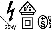
The X-radiation developing in the sets conforms to the X-radiation Regulations (January 8, 1987), issued by the Physikalisch-Technische Bundesanstalt (federal physiotechnical institution).
The high tension for the picture tube and thus the developing X-radiation depends on the precise adjustment of the +A power supply.
After every repair of the power supply unit or the horizontal deflection stage it is imperative that the EHT for the picture tube is checked and re-adjusted if necessary.
To avoid consequential damages to the chassis or the picture tube the integrated protective circuits are allowed to be put out of operation only for a short time.
When replacing the picture tube use only the types specified in the spare parts lists.

Disassembly of the chassis
Before disconnecting the chassis connecting leads observe the way they are routed to the individual assemblies like the mains switch panel, keyboard control panel, picture tube panel, deflection unit or loudspeaker.
On completion of the repairs the leads must be laid out as originally fitted at the factory to avoid later failures or disturbances.
Mains cable
The TV receiver must only be operated with an original mains connecting cable with an interference suppressor choke integrated in the mains plug. This mains cable prevents interference from the mains supply and is part of the product approval. For replacement please order exclusively the mains connecting cable specified in the spare parts list.
D Schaltplansymbole GB Circuit Diagram Symbols F Symboles schéma
Special and Service Functions
1. Special Functions
1.1 Storing the Analog Values
The entered analog values are either stored automatically after approx. 8 seconds or when switching to standby mode.
1.2 Setting the Optimum Values
Pressing "PC/AUX" "OK" the television receiver is set to the optimum values stored for brightness, contrast, colour contrast and volume.
| Optimum | Maximum | |
| Brightness | 32 | 63 |
| Colour contrast | 32 | 63 |
| BW contrast | 50 | 63 |
| Volume | 30 | 63 |
Having stored the minimum volume level, the volume setting bar is indicated on the screen for approx. 8 seconds as an optical information when switching the power "on" or switching on from standby.
1.3 ATS Start
Press and hold the "P/C/AUX" button for approx. 4s until "ATS" (Auto Tuning System) is indicated and confirm with "OK".
The ATS system stores the found station signal automatically (display: channel and finetuning).
1.4 Maximum Programme Number (reversing point):
Press the "i" -> "OK" buttons and enter "... under the frequency band selection option (B) at any programme position on the programme setting menu. Confirm with "OK" and leave the menu. As a result of this, programme selection in programme mode with the "P+/ P-" buttons is limited to the numbers lower than this position. If the reversing point is ≤ 10 only one-place programme selection is possible.
1.5 Calling up the Service Menu at "Hotel mode on"
Press and hold button "I" on the remote control and switch on with the mains button. With the "P+/P-," button select the "Hotel" mode in the menu and set the indication to "OFF" using the - or + button. During the time the "Hotel mode" is active it is not possible to call up the programme setting menu with the "PC/AUX" button.
2. Settings via the Service Menu
2.1 Calling up the Service Menu
Press and hold button "1" on the remote control and switch on with the mains button.
2.2 AGC Alignment
Select "AGC ALIGN" in the Service Menu. Alignment is possible in range 0...62 with the - / + buttons.
2.3 OSD Position
Press and hold button "1" on the remote control and switch on with the mains button. Select "OSD" (V or H) in the Service Menu and with the 12 -12 +12 buttons position the menu table in the centre of the screen.
2.4 Activating the Hotel Mode
Select "Hotel ON" in the Service Menu. When the Hotel mode is activated:
it is no longer possible to call up the programme setting menu with the "1" -> "OK" buttons.
the currently set volume level is stored as the maximum level possible in this mode.
2.5 Decoder
Via the Service Menu switch the decoder "ON" or "OFF".
Decoder "ON":
Automatic identification of the switching voltage at Pin 8 of the EURO-AV socket (e.g. descramber operation with TVs in French version, or external RGB mode for Italy).
2.6 Continuous Station Ident Indication
So that the programme name is displayed continuously on the screen press the "1" button. After about 8 seconds the programme is displayed in reduced size.
3. Settings via the AUX Menu
3.1 AUX Overview
The AUX menu is called up by pressing the "PC/AUX" remote control button quickly.
3.2 Calling up the Contrast Setting Option
Call up the AUX menu and adjust the contrast with " 己 - / 己 + " button.
3.3 Calling up the Sleeptimer
Call up the AUX menu and activate the timer with the "TXT" button. Enter the desired stop time with the numbered buttons on the remote control and leave the menu with button "1".
3.4 Optimum Values for Analog Functions
Call up the AUX menu and press "OK". The optimum values are now called up.
3.5 ATS
Call up the AUX menu and press "PC/AUX" for approximately 4s. Press the "OK" button to start the system.
3.6 Tint with NTSC
Call up the AUX menu and adjust with the button " 3 - / 3 +
Current mode converters can exhibit subharmonic oscillations when operating at a duty cycle greater than 50% with continuous inductor current. This instability is independent of the regulators closed loop characteristics and is caused by the simultaneous operating conditions of fixed frequency and peak current detecting.
Figure 1 shows the phenomenon graphically. At t_0 , switch conduction begins, causing the inductor current to rise at a slope of m_1 . This slope is a function of the input voltage divided by the inductance. At t_1 , the Current Sense Input reaches the threshold established by the control voltage. This causes the switch to turn off and the current to decay at a slope of m_2 , until the next oscillator cycle. The unstable condition can be shown if a perturbation is added to the control voltage, resulting in a small l (dashed line). With a fixed oscillator period, the current decay time is reduced, and the minimum current at switch turn-on (t_2) is increased by l + l m_2 / m_1 . The minimum current at the next cycle (t_3) decreases to ( l + l m_2 / m_1) (m_2 / m_1) . This perturbation is multiplied by m_2 / m_1 on each succeeding cycle, alternately increasing and decreasing the inductor current at switch turn-on. Several oscillator cycles may be required before the inductor current reaches zero causing the process to commence again. If m_2 / m_1 is greater than 1, the converter will be unstable. Figure 1 shows that by adding an artificial ramp that is synchronized with the PWM clock to the control voltage, the l perturbation will decrease to zero on succeeding cycles. This compensating ramp (m_3) must have a slope equal to or slightly greater than m_2 / 2 for stability. With m_2 / 2 slope compensation, the average inductor current follows the control voltage yielding true current mode operation. The compensating ramp can be derived from the oscillator and added to either the Voltage Feedback or Current Sense inputs (Figure 2).
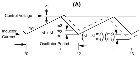
Fig. 1
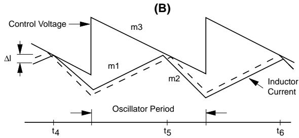
Fig. 2
1.2 Normal / Controlled Operation
For the power supply of this TV receiver a blocking oscillator-type converter power supply with a switching frequency of 50kHz approximately is used (at normal operation and a mains voltage of 230V ).
The collector contact of the power transistor T665 is connected via the primary winding 3/1 of the blocking oscillator-type transformer TR601 to the rectified mains voltage, D621...D624. At a mains voltage of 230V the voltage level present at the charging electrolytic capacitor C626 is approx. +320V.
The IC630 is responsible for driving, controlling and monitoring the bipolar power transistor T665. The supply for the control-IC is 12V and is present on Pin 7. As soon as the switch-on threshold is reached on Pin 7 via the resistor R633 and the capacitor C667, the IC feeds out a positive start pulse (1 s) of 10V_pp at Pin 6. After start-up of the IC, the supply voltage is obtained via the diode D667 from the winding 5/7 of the transformer. During the conducting phase of the transistor, energy is stored in the transformer and this is transferred into the secondary winding when the transistor is switched off. The IC630 controls by the period during which the transistor T665 is switched on, the transfer of energy at Pin 6 so that the secondary voltages are stable and are largely not affected by variations of the mains supply, mains frequency and the load.
The power transistor T665 is driven by a pulse-width modulator which is triggered by an oscillator integrated in the IC. The frequency of the oscillator is determined by the components C652 and R652. For stabilisation, the feedback voltage which is rectified by D654 is compared in IC630 with the 5V reference voltage provided at IC630-(8). If the feedback voltage decreases by a small amount due to a heavier load the drive pulse to the transistor T665 is prolonged. As a result, the conducting period of T665 will be longer so that additional energy transfer will be provided to compensate for the load. Pin 3 of IC630 is a current sense input and will stop the drive to T665 at IC630-(6) in the event of excessive current drain from a heavy secondary load.
If there was a short circuit condition at the transistor T665, the circuit UC3842 would be destroyed. Therefore, the diodes D666 and D664 are provided to avoid the voltage at pin 3 exceeding 1.2V. The components D668, C669, and R669 work as a snap stage.
The components CD654, C656, CD656, and CR656 delay the rise of the pulse start duration (soft start).
The adjustment control R654 is used to set the secondary voltages by regulating the +A voltage at minimum brightness and contrast.
1.3 Standby Mode
In normal operating mode, a voltage of approx. 10.5V is present on IC676-(1) (LM317). If the TV receiver is to be switched to standby, the P switches U_Standby to "High" level so that the level on IC676-(1) is < 0.7~V . As a result, the voltage +B is switched off and the TV receiver goes to standby.
1.4 Secondary Voltages
+A: Supply for the horizontal output stage from the winding 2/10 and D682. The power supply unit is set to this level.
+33V: The upper tuning voltage limit for the tuner is produced at the Z-diode D683 and the resistor R681 from the winding 2/10 via D682.
+M =16.5V Supply for the sound output stage from the winding 6/10 and the diode D671.
+B = 12V Power supply for the Tuner and the horizontal driver T501. This voltage is supplied from the winding 6/10 via the diode D671 and is stabilised by the adjustment control IC676. Switching off of the +12V supply, see "Standby Operation".
+E = 8V Power supply for the Video Processor IC150. In Standby mode it is switched off.
+H = 5V Power supply for the P IC850, the infrared amplifier IR810, Tuner, and CIC105. This voltage is also present in Standby mode.
Additionally necessary voltages
+D: +25V Power supply for the vertical output stage from the line transformer winding B/H via D444.
+C: 125V The power supply for the picture tube panel is obtained 190V from the line transformer winding G/H via R543 and the diode D543. 125V/14" CRT; 190V/15...21" CRT.
2. System Control
2.1 Microcomputer
The mask-programmed 8-bit Microcomputer IC850 (SDA5222 without Text) decodes the commands entered on the keyboard and also the infra-red remote control commands from the IR-receiver. It is also responsible for the total system control and the on-screen display (OSD). All data for the programme positions and the options are stored in the NVM (Non Volatile Memory). The teletext (Videotext) IC is integrated in SDA5252.
The correct operation of the microcomputer depends on the following conditions:
Supply voltage +5V / H at Pin 37
- Oscillator frequency 18MHz at Pins 12, 13
- Reset pulse:
Every time the TV receiver is switched on with the mains button, the processor is reset on Pin 1 by the reset pulse.
- I²C-bus:
The I^2C -bus is a bidirectional two-lead bus consisting of the SDA (System Data) lead and the SCL (System Clock) lead.
Checking the operation of the processor IC850:
The I^2C -bus leads are connected via the pull-up resistors CR869 and CR868 to +5V / H . The data traffic is controlled from the processor which also generates the SCL bus clock. The only way to check the data and clock leads when servicing is by measuring the TTL-levels (L ≤ 0.8V ; H ≥ 3.5V ).
Service note:
The I²C-bus data is also present without a command from the IR remote control handset. If no data is carried on the bus leads there may be a short circuit. To localize the fault, the modules and components connected to the data bus must be unsoldered or unplugged one after the other.
2.2 Initialisation of the Processor after Switching On
When the TV is switched on, the +5V / H voltage builds up, the IC850-(15) is reset, and the programme sequence is started.
With the start command, the processor feeds out a "High" level at Pin 40 and the voltage U_Standby starts the TV via CT826, IC676-(1) by means of the voltages +B, 12V (see Power Supply).
After switching on, the processor (IC850) transfers the operating data from the internal memory via the I²C-bus to the bus-controlled modules and circuits.
2.3 Switching over of the CCVS Signals to the Scart Socket
A "High"-level switching voltage UFBAS at IC850-(16) causes the CCVS signal FBASSC to be switched to output pin 19 of the Scart socket.
2.4 Entering Commands
The keyboard is connected to the unswitched voltage +5V / H . By evaluating the different voltage levels, the processor IC850-(27),-(28) knows which button on the keyboard has been pressed.
The remote control commands are amplified by the infrared receiver IC810 and decoded at Pin 8 of the microprocessor.
2.5 Teletext IC850 (SDA5252)
The IC850 (SDA5252) contains a 1-page Teletext-IC. The On Screen Display is subdivided into lines and columns. For positioning and synchronising the teletext display, horizontal and vertical reference pulses are fed to IC850-(45, 46). Activation of the teletext is effected internally via the I²C-bus. Via pin 30, the SDA5252 scans the CCVS signal for teletext data.
2.6 On Screen Display (OSD)
For displaying data on the screen, the switching voltage "U Data" IC850-(50) supplies a "High" level switching IC150-(21) ≤ 2V to RGB mode. The character generator feeds out the display data via the output ports 47, 48, 49 of the microprocessor at an amplitude of 4.5V to the RGB inputs IC150-(22), -(23), -(24), approx. 450mV.
2.7 Protection Circuit U,
The base of the transistor T511 is connected via R511 to the low-end point of the vertical output stage, and via R512, D512, D513 to the reference pulse F from the horizontal output stage. In the case of any failure, a base voltage of 0.6V and higher switches the transistor on; via its collector the transistor switches IC850-(32) to ground. The P then switches the TV to standby.
If the voltage +D fails there is no direct voltage present at the output of the vertical output stage IC400-(5) and consequently the protection circuit input IC850-(32) is pulled to ground.
At the same time the collector (SB lead) is connected via R513, D514, and CD516 to the low-end point of the high-tension winding. When the Zener voltage is exceeded due to too high a beam current the collector voltage decreases to 0V so that the TV switches to standby.
3. TV Signal Processor TDA8362A
3.1 Overview:
With this TV design the whole signal processing is carried out in a single IC, i.e. the TV Signal Processor TDA 8362A. It accommodates the following stages:
IF Signal:
- IF amplifier
- Demodulator
- AFC
- AGC
- Coincidence identification
CCVS Signal:
- Signal source switch for the CCVS signal
- Luminance processing
-Colour demodulation - Chrominance processing
Colour contrast control
RGB matrix - C-AV input
- Signal source switch for RGB signals
- Brightness control
- Contrast control
- Black level control (cut-off)
Sound:
- Signal source switch for the sound
Sound demodulation
Volume control
Deflection:
- Sync separator
- Line oscillator
- 1 phase control
- 2 phase control
- Trigger pulse generation for the line output stage
- Line counter
- Saw-tooth generation for the vertical deflection
- Drive signal for the field output stage
Dependent on the associated circuitry, the IC is also able to process PAL, NTSC and SECAM signals.
3.2 IF
The IF spectrum of frequencies is fed through a symmetrical path from the tuner Pins 11 and 10 via the filter F901 and the Surface Acoustic Wave filter F906. The signal formed by the Surface Acoustic Wave filter is applied symmetrically to Pins 45 and 46 of the signal processor. The demodulation of the CCVS signal is carried out in a product demodulator.
The required demodulator circuit F130 is connected to Pin 2 and Pin 3. The demodulated signal passes through an amplifier and is then present at Pin 7 of the IC (BB). The IC identifies the synchronising signal internally and for this reason, feedback of the line flyback pulse for gating purposes is not necessary. Corresponding to the synchronising signal level a control voltage is generated. This control voltage first acts on the controlled input amplifier of the IF. Via Pin 49 a reference threshold U_RV is set. Below this threshold, only the input amplifier of the IF is regulated. If the threshold is exceeded, the control voltage U_t is applied from Pin 47 to the tuner. Pin 47 is an open collector output. In uncontrolled condition, the voltage is approximately 5V. With increasing input amplitude the AGC level decreases. The direct voltage for automatic frequency control (AFC) is generated in the demodulator. Pin 9 feeds out this signal as a current signal. When the received frequency increases the control voltage for AFC decreases. The processor IC850 evaluates the signal and fine tunes the tuner accordingly. The demodulated signal is examined by the sync detector for the presence of synchronising signals. If no such signals are present, the IC150-(4) switches to "Low". By this level the processor IC850-(33) can identify that the coincidence signal is missing and mutes the sound.
3.3 CCVS Signal
The demodulated CCVS signal leaves IC150-(7), TDA8362A, as a baseband signal together with the sound-IF. In the following path, the sound signal is separated from the CCVS signal. After the transistor CT921 and the sound trap F923 and F924 the signal path divides.
Via the transistor CT110 and IC2807 (optionally) it is fed through to the videotext decoder IC850-(30) as FBAS_SC signal, and via the transistors CT963, CT962 it is supplied to the Scart socket pin 19.
At the signal source switch IC150-(13), the signal is present as FBAS (CCVS). The second input of the signal source switch Pin 15 is connected to the Scart socket pin 20.
At IC150-(16), the processor IC850-(42), voltage U_VQ , transistor CT840 decides as to whether the signal from the tuner or the external signal is processed.
3.4 External CCVS Signal
At the signal source switch IC150-(15) either an external CCVS signal from the Scart socket or the RF-CCVS signal is present. The voltage U_VQ at IC150-(16) decides which signal shall be passed on, the CCVS signal from the Scart socket or else the RF-CCVS signal. IC150-(16) "Low", the internal signal is selected; IC150-(16) "High", the external signal is passed on.
Attention: If the option "Decoder On" has been selected the TV expects the signal to come from the Scart socket. However the CCVS signal from the tuner can be measured at output Pin 19 of the Scart socket.
After the ceramic filter F926, the sound signal is superimposed at IC150-(5) on a direct voltage for setting the volume level. Demodulation is effected by a PLL demodulator.
In one path, the demodulated and uncontrolled AF signal is fed out at IC150-(1), it is then amplified by the transistors CT917, CT916 and passed on to the Scart socket.
In another path, the demodulated and controlled AF signal is present at IC150-(50) and is fed to the AF-IC TDA7233.
3.6 Luminance and Chrominance Signal
Calibration and control is effected automatically during the frame blanking period. The signals are adjusted by a positive or negative current entering the integration capacitor CC177 at IC150-(12). During the scanning period the control voltage is clamped.
The luminance signal passes through the colour trap integrated in the IC. The delay line provided in the IC is used to correct delay time differences between the luminance and chrominance signal. The colour transient improvement (peaking) which follows is also realized in this IC. For this, the steepness of the leading and trailing edges of the Y-signal is improved. The internal chroma filter separates the chrominance signal from the CCVS signal. A control circuit adjusts the amplitude of the colour signal for the chroma limiter and chroma control. The resulting chroma signal is passed on to the colour demodulator. From this chroma signal, the burst is separated which is used to synchronise the colour oscillator in phase and frequency. The quartz establishes a fixed 4.43MHz frequency for the colour carrier at Pin 35. The quartz is controlled by an internal PLL circuit. The correction voltage is integrated via the time constant at Pin 33. By means of the colour carrier, the colour component signals are then
demodulated and leave IC150 as R-Y and B-Y signals at Pin 30 and Pin 31 respectively. Following the PAL delay at CIC105 TDA4665 the two signals, B-Y and R-Y, are fed back to IC150-(28), -(29) TDA8362A where they are clamped.
Subsequently, the colour contrast is controlled at IC150-(26). In the matrix, the RGB signals are produced from the amplified signals and the Y-component.
3.7 SECAM Signal Path and Automatic PAL-SECAM Switching
The chroma signal of approx. 300mV for the SECAM-IC110 is present at IC150-(27).
On SECAM mode, a voltage between 5.6V...5.8V is applied to IC110-(16). When the IC110 identifies the SECAM standard from the chroma signal at pin 16, a current source at pin 1 is activated and sends a SECAM identification to IC150-(32). As soon as IC150 too has identified SECAM, this IC sets pin 32 to 5V (1.5V on PAL). This direct voltage is superimposed either by a regular clock frequency on PAL, or by bursts at a frequency of 4.43 MHz on SECAM.
The IC110 interprets these as an acknowledgement and switches the difference signal outputs R-Y and B-Y (pins 9 and 10) to 3.5V DC (1.5V on PAL). The difference signal outputs of IC150-(30), -(31) are thus blocked. IC110 now supplies the R-Y and B-Y signals. The difference signals are returned to IC150 via the delay line CIC105. The following path of these signals is described under 3.6 "Luminance and Chrominance Signal".
On SECAM reception the DC Level is switched to 3.5V at IC110-(10). Via CT115, U_PAL changes to "Low" (PAL="High") and P IC850-(1) is able to identify PAL or SECAM on ATS search (only FR variants).
On OIRT reception (6.5MHz sound carrier), the search mode of the P (UPAL) is switched over by CT915 via UAUDIO and CT115.
3.8 RGB Signal Path
For contrast control of the RGB signals, IC850-(23) generates a variable control voltage for the contrast controlling amplifier at IC150-(25). Because too high a beam current may cause damage to the picture tube, the beam current is limited by this IC. The internal peak beam current limiting function is carried out in the peak white limiting stage. If the RGB signal exceeds 2.6V_pp , the internal peak white limiting function starts working and reduces the contrast. The external peak beam current limiting threshold is 2V_pp approximately.
The average beam current limiting function reduces the setting voltages at IC150-(25) for the contrast.
After the brightness amplifier, the RGB signals leave the IC150 and are passed on to the cathode amplifiers on the CRT base panel.
3.9 Generation of the Horizontal and Vertical Sync Signals
The TV signal processor IC150-(13,15) is connected to the CCVS signal from the IF and from the EURO-AV socket. Following an internal colour trap where the colour information is filtered off the CCVS signal, the resulting Y-signal now divides into two paths. In one path the signal is passed on for further processing, and in the other, the signal is applied to the sync separator.
The sync separator produces the horizontal and the vertical synchronising pulses from the Y-signal. The horizontal synchronising signal is passed on to the 1 phase control, the vertical synchronising pulse is used to start the line counter for vertical synchronisation.
3.10 Line Oscillator
With this IC concept, the line frequency is generated completely inside the line oscillator. The IC is not connected to external components so that it is not necessary to adjust the free running horizontal and the free running vertical frequency.
3.11 1 Phase Control
The 1 phase control stage is for controlling the frequency. This stage adjusts the frequency of the line oscillator to that of the line synchronising pulse. For this, the frequency of the line synchronising pulse is compared with the line oscillator frequency.
A 1 phase control stage defines the time constant of the control voltage which is fed out at IC150-(40). The control voltage shifts the line oscillator until the frequencies are equal.
3.12 2 Phase Control
The 2 phase control stage is for controlling the phase position of the line drive pulse. This determines the phase off-set between the line synchronising pulses and the actual position of the electron beam. Dependent on the circuit components and the beam current, the delay time between the external signal, the trigger signal and the actual reaction of the line output stage is different. These differences are compensated for by the 2 control.
To identify the position of the electron beam the line flyback pulse from the line output transformer is applied to IC150-(38). From the oscillator signal and the line flyback pulse the 2 controlling stage produces a control voltage at IC150-(39) which is filtered by CC166.
3.13 The Super Sand Castle - SSC
The 3-level SSC signal IC150-(38) is a composite pulse consisting of the line flyback, the field flyback, and the burst key pulses. The line flyback pulse (H-Sync) is fed through T523, CR163 to IC150. The field flyback and burst key pulses are generated inside the IC.
If the field deflection stage fails, IC400-(7) pulls the SSC level to "Low" via R401 and thus blanks the CRT at IC150-(18, 19, 20) RGB. In doing so, the analog values are set to "Low".
3.14 Setting of the Cut Off Voltage
An automatic cut-off controlling stage ensures that the static working points of the CRT are held stable. For this, IC150 feeds out a pulse to the R, G, B cathodes during the lines 23, 24 and 25 to measure the beam current of each system (approx. 10 A ). The cut-off current during the measuring lines is fed via the resistor CR156 to IC150-(14). The IC compares this voltage with an internal reference value to determine the working point for the black level of the video output stages and the cut-off voltage of the CRT respectively.
3.15 The HDR Output Stage
Following an amplification stage the horizontal drive signal for the line output transistor is provided at Pin 37.
3.16 The Field Deflection Stage
In this circuit concept, the field sync generator is substituted by a line counter.
When no synchronising signals are received the line oscillator is free running. From this line oscillator the "vertical oscillator" is derived by counting the number of lines. After having counted 312 lines, the counter feeds out a field sync signal so that the horizontal and also the vertical deflection is achieved without using an external synchronising signal.
On reception of a synchronising signal, the line oscillator will first be synchronised. In this case too, the line counter supplies a field deflection signal. As soon as a field synchronising signal is obtained the saw-tooth generator will no longer be triggered by the line counter but directly by the field sync signal.
The saw-tooth generator is made up of a constant current source which is used to charge and discharge an external capacitor. The charging period is determined by the field sync signal. The field deflection signal can be measured at the capacitor C158, IC150-(43).
Adjustment of the field amplitude at the field output stage IC400 is possible by influencing the field saw-tooth voltage. This alteration must be carried out before the field output stage. For this, a feedback signal from IC400 is present at IC150-(42) for negative feedback. Similar to an operational amplifier connected to the negative input, this technique allows to set the desired parameters.
3.17 Non-Interlace Compensation with Teletext (25Hz Modulation) When a teletext (videotext) signal is displayed on the screen, the teletext signal would continuously change by one line upwards and downwards (non-interlaced teletext signal). To avoid the signal changing the line, the teletext IC850-(52) supplies a 25Hz switching signal to IC150-(43). From this U_25Hz switching voltage, a small DC voltage offset is derived for the deflection saw-tooth. This offset effects an upward shift of the first half-field so that the even-numbered and odd-numbered lines are superimposed on each other.
3.18 Coincidence
The coincidence information is generated in the IF stage and fed out on IC150-(4).

All adjustment controls not mentioned in this description are adjusted during production and must not be re-adjusted in the case of repairs.
Measuring Instruments: Oscilloscope with 10:1 test probe, colour test pattern, high resistance voltmeter
Checks and adjustments after replacement or repair of:
Power Supply: 1.
Horizontal Deflection: 2., 3.
Picture Tube, CRT-Panel: 2., 6.
IC150: 4., 5.
Tuner: 4., 5.
| Alignment | Preparations | Alignment Process |
| 1. +A Voltage | Set luminance to minimum. Connect the voltmeter to the cathode of D682. | With control R654 set the voltage to 112V (14" Orion), 105V (14" Philips), 124V (15...21"). |
| 2. Screen grid voltage Ug2 | Feed in a grey scale test pattern. Adjust the screen brightness so that the gradation from the darkest grey scale value to black is just still visible (2.7V to IC150-(17)). Set the contrast (Ø) to mid-value. Measure test points R, G, B (on the CRT panel) to determine the test point with the highest black level and connect this point to the oscilloscope. | With the control Ug2 adjust the black level at the test point with the highest black level to approx. 100V...105V for 14" picture tubes and 150V...155V for 15...21" picture tubes. Black level 100V...105V 14" 150V...155V 15...21" |
| 3. Line sharpness | Select the convergence test pattern. Contrast (Ø) to maximum. Set the brightness so that the black background of the test pattern is just brightening. | With the focus control Uf on the focusing panel adjust the horizontal lines for maximum sharpness. |
| 4. Vision demodulator (vision carrier 38.9 MHz) | Feed in a generator with vision carrier 38.9MHz ca. 120mV on tuner contact 10, 11. Vision carrier 38.9 MHz. Norm 1 via Menu ("i" -> "OK") Voltmeter: IC850-(34) | With filter F130 set the DC level to 2.5V. With trimmer C136 set the DC level to 2.5V. Repeat mutual adjustments! |
| Vision demodulator French standard (vision carrier 33.4MHz) | Feed in a generator with vision carrier 33.4MHz ca. 120mV on tuner contact 10, 11. Norm 3 via Menu ("i" -> "OK") Voltmeter: IC850-(34) | |
| 5. Tuner AGC | Feed in a standard test pattern at a channel in the upper range of the UHF band and store it at programme position 1. RF = 1.5mV (64dBμV, noise-free picture). Switch the TV off with the power button. Call up the Service Menu with remote control. (press and hold the button "i" and switching the TV on). With "P+/P-" buttons select the menu item "AGC ALIGN". | With the "- or +" buttons tune the station so that noise just starts to appear in the picture. Then reduce the value so that the noise just disappears from the picture. Terminate with "i". |
| 6. White balance | Feed in a FuBK test pattern. Set the colour contrast (Ø) to minimum. Set the contrast (Ø) to maximum. Adjust the screen brightness (Ø) so that the gradation from the darkest grey scale value to black is just still visible. | Set the controls VG and VB on the CRT panel so that no discolouration is visible in the grey scale. |
Coordinates of the Components on the Components Side (Top Side)
| Pos. N°/Pos. No. | Coordonnées/Coordinates | |
| X | Y | |
| AN10 | 348 | 255 |
| AN11 | 5 | 255 |
| AN12 | 5 | 5 |
| AN13 | 5 | 90 |
| AN14 | 162 | 147 |
| AN15 | 348 | 90 |
| AN16 | 348 | 5 |
| AN30 | 9 | 10 |
| AN31 | 239 | 10 |
| BR-HZ | 121 | 171 |
| BR01 | 245 | 133 |
| BR03 | 136 | 24 |
| BR07 | 238 | 79 |
| BR13 | 251 | 137 |
| BR14 | 23 | 119 |
| BR16 | 150 | 135 |
| BR17 | 146 | 133 |
| BR18 | 45 | 91 |
| BR24 | 31 | 131 |
| BR25 | 19 | 61 |
| BR26 | 146 | 106 |
| BR27 | 241 | 124 |
| BR31 | 19 | 59 |
| BR33 | 123 | 96 |
| BR34 | 29 | 79 |
| BR36 | 91 | 38 |
| BR38 | 122 | 94 |
| BR39 | 151 | 73 |
| BR40 | 30 | 101 |
| BR41 | 31 | 104 |
| BR42 | 31 | 99 |
| BR43 | 35 | 76 |
| BR44 | 33 | 94 |
| BR45 | 185 | 118 |
| BR48 | 224 | 90 |
| BR49 | 42 | 89 |
| BR50 | 204 | 123 |
| BR51 | 173 | 69 |
| BR52 | 170 | 71 |
| BR53 | 167 | 69 |
| BR54 | 24 | 117 |
| BR55 | 175 | 62 |
| BR56 | 159 | 95 |
| BR57 | 163 | 26 |
| BR58 | 43 | 86 |
| BR59 | 179 | 110 |
| BR61 | 164 | 64 |
| BR62 | 126 | 70 |
| BR63 | 174 | 19 |
| BR64 | 177 | 19 |
| BR67 | 100 | 31 |
| BR68 | 114 | 16 |
| BR69 | 90 | 20 |
| BR70 | 119 | 16 |
| BR73 | 208 | 105 |
| BR74 | 234 | 101 |
| BR77 | 164 | 124 |
| BR79 | 192 | 19 |
| BR80 | 207 | 29 |
| BR81 | 168 | 22 |
| BR82 | 166 | 21 |
| BR84 | 182 | 19 |
| BR86 | 187 | 18 |
| BR88 | 43 | 51 |
| BR89 | 186 | 53 |
| BR99 | 160 | 18 |
| BR100 | 152 | 39 |
| BR101 | 155 | 38 |
| BR105 | 130 | 38 |
| BR106 | 127 | 146 |
| BR109 | 98 | 31 |
| BR111 | 81 | 25 |
| BR113 | 56 | 116 |
| BR114 | 124 | 71 |
| BR115 | 125 | 19 |
| BR116 | 132 | 40 |
| Pos. N°/Pos. No. | Coordonnées/Coordinates | |
| X | Y | |
| BR117 | 65 | 29 |
| BR119 | 30 | 96 |
| BR120 | 33 | 81 |
| BR121 | 68 | 34 |
| BR122 | 25 | 33 |
| BR123 | 40 | 73 |
| BR125 | 28 | 16 |
| BR128 | 32 | 59 |
| BR129 | 17 | 54 |
| BR130 | 138 | 231 |
| BR132 | 61 | 54 |
| BR135 | 35 | 63 |
| BR136 | 35 | 66 |
| BR139 | 59 | 116 |
| BR141 | 9 | 51 |
| BR145 | 133 | 133 |
| BR148 | 44 | 71 |
| BR149 | 110 | 126 |
| BR150 | 114 | 129 |
| BR151 | 96 | 75 |
| BR152 | 108 | 70 |
| BR153 | 93 | 70 |
| BR154 | 92 | 68 |
| BR155 | 131 | 116 |
| BR156 | 131 | 114 |
| BR157 | 129 | 111 |
| BR159 | 42 | 68 |
| BR160 | 51 | 115 |
| BR161 | 54 | 116 |
| BR162 | 62 | 115 |
| BR164 | 25 | 136 |
| BR166 | 27 | 147 |
| BR167 | 26 | 159 |
| BR168 | 59 | 139 |
| BR169 | 76 | 138 |
| BR170 | 82 | 154 |
| BR171 | 81 | 136 |
| BR172 | 102 | 128 |
| BR173 | 123 | 154 |
| BR174 | 126 | 156 |
| BR175 | 81 | 60 |
| BR176 | 114 | 201 |
| BR177 | 94 | 214 |
| BR178 | 89 | 221 |
| BR179 | 76 | 223 |
| BR181 | 69 | 237 |
| BR182 | 200 | 198 |
| BR183 | 121 | 131 |
| BR184 | 170 | 202 |
| BR185 | 129 | 159 |
| BR186 | 159 | 199 |
| BR187 | 72 | 178 |
| BR189 | 72 | 174 |
| BR190 | 94 | 164 |
| BR198 | 158 | 11 |
| BR200 | 208 | 47 |
| BR201 | 163 | 11 |
| BR204 | 213 | 57 |
| BR205 | 146 | 10 |
| BR206 | 58 | 148 |
| BR207 | 204 | 40 |
| BR208 | 242 | 109 |
| BR209 | 201 | 118 |
| BR210 | 189 | 98 |
| BR211 | 258 | 84 |
| BR212 | 253 | 78 |
| BR213 | 191 | 41 |
| BR214 | 214 | 60 |
| BR215 | 180 | 23 |
| BR216 | 177 | 62 |
| BR217 | 222 | 6 |
| BR218 | 222 | 11 |
| BR219 | 224 | 9 |
| BR220 | 184 | 24 |
| BR221 | 189 | 114 |
| BR222 | 235 | 114 |
| Pos. N°/Pos. No. | Coordonnées/Coordinates | |
| X | Y | |
| BR223 | 263 | 83 |
| BR224 | 208 | 135 |
| BR225 | 246 | 24 |
| BR226 | 187 | 95 |
| BR227 | 180 | 78 |
| BR228 | 177 | 83 |
| BR324 | 88 | 24 |
| BR325 | 72 | 20 |
| BR526 | 18 | 200 |
| BR531 | 51 | 190 |
| BR532 | 95 | 188 |
| BR533 | 72 | 194 |
| BR546 | 82 | 223 |
| BR600 | 220 | 224 |
| BR601 | 221 | 219 |
| BR641 | 142 | 208 |
| BR646 | 148 | 245 |
| BR663 | 176 | 226 |
| BR671 | 98 | 230 |
| BR891 | 213 | 124 |
| BR892 | 210 | 113 |
| C106 | 160 | 34 |
| C108 | 146 | 46 |
| C112 | 135 | 46 |
| C115 | 169 | 48 |
| C127 | 50 | 54 |
| C128 | 58 | 62 |
| C129 | 47 | 61 |
| C136 | 61 | 84 |
| C141 | 89 | 85 |
| C145 | 67 | 63 |
| C148 | 53 | 60 |
| C149 | 80 | 86 |
| C151 | 148 | 73 |
| C152 | 140 | 73 |
| C153 | 145 | 80 |
| C158 | 92 | 54 |
| C167 | 99 | 46 |
| C191 | 141 | 89 |
| C302 | 33 | 54 |
| C303 | 18 | 30 |
| C309 | 41 | 56 |
| C323 | 50 | 17 |
| C325 | 96 | 16 |
| C326 | 43 | 16 |
| C327 | 71 | 17 |
| C331 | 47 | 25 |
| C402 | 65 | 163 |
| C408 | 18 | 144 |
| C412 | 82 | 162 |
| C417 | 85 | 191 |
| C422 | 59 | 168 |
| C444 | 96 | 175 |
| C446 | 108 | 174 |
| C501 | 29 | 139 |
| C502 | 43 | 169 |
| C503 | 48 | 159 |
| C506 | 28 | 180 |
| C511 | 64 | 131 |
| C512 | 201 | 137 |
| C513 | 61 | 125 |
| C522 | 38 | 196 |
| C526 | 28 | 189 |
| C527 | 10 | 207 |
| C532 | 68 | 252 |
| C541 | 73 | 214 |
| C542 | 68 | 214 |
| C543 | 116 | 193 |
| C601 | 221 | 203 |
| C603 | 229 | 164 |
| C604 | 238 | 165 |
| C609 | 211 | 174 |
| C621 | 191 | 199 |
| C622 | 195 | 175 |
| C623 | 191 | 192 |
| C624 | 191 | 176 |
| Pos. N°/Pos. No. | Coordonnées/Coordinates | |
| X | Y | |
| C626 | 150 | 179 |
| C626 | 150 | 179 |
| C627 | 130 | 203 |
| C646 | 156 | 241 |
| C647 | 152 | 202 |
| C652 | 168 | 179 |
| C653 | 166 | 183 |
| C656 | 174 | 174 |
| C661 | 182 | 205 |
| C663 | 176 | 225 |
| C664 | 144 | 194 |
| C667 | 184 | 225 |
| C669 | 155 | 233 |
| C671 | 104 | 221 |
| C672 | 107 | 210 |
| C676 | 173 | 139 |
| C681 | 101 | 242 |
| C682 | 87 | 245 |
| C682 | 87 | 245 |
| C683 | 28 | 108 |
| C687 | 38 | 129 |
| C695 | 155 | 139 |
| C811 | 258 | 172 |
| C818 | 195 | 103 |
| C819 | 196 | 111 |
| C827 | 203 | 55 |
| C851 | 180 | 41 |
| C863 | 140 | 139 |
| C911 | 48 | 79 |
| C921 | 116 | 26 |
| C922 | 110 | 26 |
| C923 | 105 | 45 |
| C924 | 95 | 39 |
| C966 | 173 | 84 |
| C2810 | 168 | 89 |
| C2815 | 175 | 103 |
| C2816 | 183 | 103 |
| C2817 | 185 | 105 |
| C2856 | 197 | 26 |
| C2858 | 11 | 31 |
| C3331 | 48 | 25 |
| CH01 | 267 | 58 |
| CO626 | 150 | 178 |
| D323 | 104 | 13 |
| D324 | 94 | 24 |
| D401 | 69 | 157 |
| D405 | 73 | 137 |
| D406 | 64 | 154 |
| D444 | 100 | 175 |
| D512 | 127 | 136 |
| D513 | 117 | 184 |
| D514 | 191 | 137 |
| D524 | 55 | 195 |
| D543 | 91 | 219 |
| D621 | 190 | 168 |
| D622 | 191 | 162 |
| D623 | 190 | 187 |
| D624 | 188 | 178 |
| D646 | 151 | 237 |
| D647 | 151 | 222 |
| D661 | 175 | 199 |
| D662 | 163 | 204 |
| D663 | 164 | 217 |
| D664 | 180 | 233 |
| D666 | 180 | 240 |
| D667 | 148 | 206 |
| D668 | 156 | 209 |
| D671 | 101 | 226 |
| D682 | 104 | 237 |
| D683 | 25 | 114 |
| D816 | 274 | 194 |
| D816 | 272 | 194 |
| D826 | 171 | 14 |
| ENTMAG | 213 | 164 |
| Pos. N°/Pos. No. | Coordonnées/Coordinates | |
| X | Y | |
| F130 | 71 | 84 |
| F901 | 67 | 53 |
| F906 | 80 | 51 |
| F923 | 89 | 109 |
| F924 | 89 | 94 |
| F926 | 69 | 96 |
| F927 | 73 | 96 |
| F931 | 80 | 40 |
| IC110 | 144 | 55 |
| IC150 | 95 | 70 |
| IC320 | 59 | 20 |
| IC400 | 60 | 151 |
| IC630 | 167 | 190 |
| IC676 | 108 | 153 |
| IC690 | 141 | 153 |
| IC810 | 282 | 173 |
| IC810 | 277 | 173 |
| IC820 | 196 | 60 |
| IC830 | 172 | 40 |
| IC850 | 204 | 76 |
| IC950 | 110 | 36 |
| IC2807 | 166 | 99 |
| IR-BA | 265 | 184 |
| KB | 265 | 169 |
| KH335 | 269 | 36 |
| KH3335 | 273 | 85 |
| L+ | 264 | 139 |
| L- | 264 | 154 |
| L108 | 158 | 53 |
| L301 | 29 | 30 |
| L302 | 38 | 30 |
| L303 | 32 | 30 |
| L305 | 56 | 54 |
| L381 | 260 | 36 |
| L506 | 20 | 195 |
| L526 | 18 | 200 |
| L531 | 50 | 180 |
| L533 | 72 | 194 |
| L543 | 86 | 223 |
| L601 | 233 | 189 |
| L601 | 231 | 187 |
| L601- | 231 | 187 |
| L641 | 142 | 208 |
| L646 | 148 | 246 |
| L817 | 198 | 93 |
| L818 | 181 | 90 |
| L819 | 199 | 121 |
| L912 | 155 | 66 |
| L924 | 90 | 100 |
| L2836 | 204 | 94 |
| L3381 | 261 | 93 |
| NETZ | 211 | 243 |
| P+ | 264 | 106 |
| P- | 264 | 121 |
| P01 | 34 | 18 |
| Q171 | 106 | 56 |
| Q172 | 99 | 56 |
| Q857 | 205 | 64 |
| R118 | 125 | 48 |
| R119 | 123 | 51 |
| R156 | 43 | 139 |
| R166 | 16 | 22 |
| R183 | 100 | 101 |
| R203 | 256 | 29 |
| R303 | 61 | 26 |
| R337 | 81 | 19 |
| R401 | 79 | 135 |
| R404 | 46 | 138 |
| R406 | 73 | 169 |
| R408 | 11 | 156 |
| R411 | 9 | 166 |
| Pos. N°/Pos. No. | Coordonnées/Coordinates | |
| X | Y | |
| R412 | 70 | 171 |
| R413 | 11 | 146 |
| R414 | 16 | 137 |
| R416 | 86 | 179 |
| R442 | 107 | 192 |
| R502 | 45 | 164 |
| R503 | 28 | 155 |
| R504 | 35 | 166 |
| R506 | 9 | 176 |
| R511 | 70 | 136 |
| R512 | 68 | 125 |
| R512 | 70 | 125 |
| R513 | 195 | 139 |
| R521 | 16 | 158 |
| R522 | 13 | 179 |
| R524 | 56 | 199 |
| R526 | 20 | 203 |
| R531 | 51 | 190 |
| R532 | 95 | 189 |
| R533 | 73 | 206 |
| R542 | 117 | 133 |
| R543 | 79 | 224 |
| R546 | 82 | 223 |
| R553 | 116 | 167 |
| R554 | 94 | 214 |
| R554 | 96 | 214 |
| R609 | 209 | 187 |
| R621 | 197 | 199 |
| R627 | 166 | 165 |
| R633 | 186 | 215 |
| R647 | 143 | 212 |
| R651 | 175 | 184 |
| R652 | 180 | 181 |
| R653 | 177 | 184 |
| R654 | 181 | 196 |
| R661 | 184 | 236 |
| R663 | 166 | 203 |
| R664 | 145 | 206 |
| R665 | 171 | 225 |
| R666 | 161 | 241 |
| R667 | 164 | 241 |
| R669 | 155 | 209 |
| R681 | 91 | 172 |
| R683 | 28 | 124 |
| R685 | 50 | 128 |
| R2203 | 256 | 84 |
| R4414 | 21 | 133 |
| RGB | 107 | 101 |
| S601 | 241 | 219 |
| SCART01 | 6 | 93 |
| SI600 | 231 | 239 |
| SI671 | 94 | 233 |
| ST-BAT01 | 230 | 73 |
| ST-BAT03 | 105 | 143 |
| ST-BAT04 | 83 | 212 |
| ST-BAT02 | 71 | 244 |
| ST-J | 69 | 182 |
| ST-NetzZ02 | 212 | 221 |
| T501 | 39 | 160 |
| T506 | 9 | 189 |
| T511 | 75 | 124 |
| T523 | 139 | 131 |
| T665 | 172 | 229 |
| T686 | 40 | 122 |
| TR501 | 25 | 168 |
| TR550 | 37 | 227 |
| TR601 | 129 | 232 |
| TRX550 | 37 | 227 |
| TUNER | 30 | 42 |
Chassis Board
Coordinates of the components on the Solder Side (Bottom Side)
| Pos. N°/Pos. No. | Coordonnées/Coordinates | |
| X | Y | |
| CR155 | 88 | 52 |
| CR156 | 100 | 84 |
| CR158 | 89 | 67 |
| CR159 | 101 | 65 |
| CR161 | 89 | 56 |
| CR162 | 53 | 105 |
| CR163 | 85 | 129 |
| CR164 | 20 | 21 |
| CR165 | 93 | 47 |
| CR166 | 95 | 49 |
| CR167 | 96 | 55 |
| CR168 | 86 | 54 |
| CR169 | 49 | 104 |
| CR171 | 102 | 60 |
| CR173 | 105 | 66 |
| CR174 | 120 | 64 |
| CR175 | 120 | 60 |
| CR181 | 98 | 102 |
| CR182 | 96 | 102 |
| CR183 | 99 | 89 |
| CR186 | 105 | 89 |
| CR187 | 149 | 88 |
| CR191 | 136 | 83 |
| CR192 | 134 | 87 |
| CR193 | 147 | 88 |
| CR194 | 132 | 91 |
| CR304 | 43 | 33 |
| CR305 | 35 | 38 |
| CR306 | 26 | 72 |
| CR307 | 24 | 72 |
| CR309 | 41 | 60 |
| CR313 | 22 | 36 |
| CR314 | 28 | 36 |
| CR315 | 25 | 38 |
| CR321 | 68 | 21 |
| CR322 | 53 | 15 |
| CR323 | 91 | 19 |
| CR324 | 98 | 17 |
| CR325 | 60 | 13 |
| CR326 | 41 | 20 |
| CR327 | 100 | 17 |
| CR328 | 45 | 20 |
| CR329 | 58 | 20 |
| CR331 | 41 | 22 |
| CR381 | 257 | 27 |
| CR382 | 263 | 27 |
| CR402 | 39 | 133 |
| CR403 | 65 | 168 |
| CR404 | 73 | 162 |
| CR405 | 74 | 127 |
| CR406 | 15 | 150 |
| CR407 | 16 | 137 |
| CR408 | 17 | 134 |
| CR409 | 65 | 146 |
| CR411 | 131 | 131 |
| CR412 | 145 | 122 |
| CR419 | 6 | 149 |
| CR523 | 63 | 134 |
| CR541 | 106 | 121 |
| CR641 | 142 | 208 |
| CR654 | 173 | 182 |
| CR656 | 177 | 184 |
| CR673 | 100 | 155 |
| CR674 | 103 | 162 |
| CR686 | 43 | 118 |
| CR687 | 38 | 125 |
| CR801 | 257 | 121 |
| CR802 | 261 | 129 |
| CR803 | 238 | 111 |
| CR804 | 261 | 131 |
| CR805 | 257 | 154 |
| CR806 | 190 | 94 |
| CR808 | 189 | 102 |
| CR811 | 260 | 181 |
| CR813 | 200 | 94 |
| CR816 | 260 | 186 |
| CR817 | 251 | 165 |
| CR818 | 183 | 88 |
| CR819 | 258 | 184 |
| CR820 | 224 | 64 |
| CR821 | 223 | 105 |
| CR822 | 217 | 96 |
| CR823 | 227 | 96 |
| CR824 | 222 | 96 |
| CR825 | 222 | 79 |
| CR826 | 209 | 101 |
| CR827 | 201 | 72 |
| CR828 | 206 | 73 |
| CR829 | 203 | 72 |
| CR830 | 249 | 127 |
| CR831 | 219 | 79 |
| CR832 | 184 | 53 |
| CR833 | 215 | 105 |
| Pos. N°/Pos. No. | Coordonnées/Coordinates | |
| X | Y | |
| CR834 | 210 | 87 |
| CR835 | 193 | 72 |
| CR836 | 191 | 72 |
| CR837 | 188 | 33 |
| CR838 | 184 | 95 |
| CR839 | 188 | 91 |
| CR840 | 180 | 53 |
| CR841 | 180 | 111 |
| CR843 | 182 | 53 |
| CR844 | 189 | 57 |
| CR845 | 217 | 79 |
| CR846 | 184 | 57 |
| CR847 | 175 | 39 |
| CR848 | 182 | 57 |
| CR849 | 170 | 57 |
| CR850 | 189 | 72 |
| CR851 | 190 | 53 |
| CR852 | 175 | 60 |
| CR853 | 167 | 57 |
| CR854 | 170 | 65 |
| CR855 | 175 | 65 |
| CR856 | 186 | 63 |
| CR857 | 204 | 64 |
| CR858 | 211 | 134 |
| CR859 | 187 | 72 |
| CR860 | 213 | 79 |
| CR861 | 224 | 72 |
| CR862 | 193 | 80 |
| CR863 | 191 | 80 |
| CR864 | 226 | 64 |
| CR865 | 227 | 73 |
| CR866 | 235 | 78 |
| CR867 | 222 | 61 |
| CR868 | 172 | 30 |
| CR869 | 166 | 22 |
| CR870 | 215 | 59 |
| CR873 | 216 | 65 |
| CR875 | 215 | 79 |
| CR876 | 195 | 80 |
| CR877 | 194 | 49 |
| CR878 | 222 | 64 |
| CR879 | 208 | 79 |
| CR880 | 192 | 87 |
| CR881 | 232 | 86 |
| CR882 | 236 | 86 |
| CR883 | 210 | 79 |
| CR891 | 211 | 114 |
| CR892 | 211 | 112 |
| CR901 | 70 | 45 |
| CR902 | 81 | 47 |
| CR903 | 128 | 25 |
| CR904 | 66 | 53 |
| CR905 | 147 | 19 |
| CR906 | 149 | 19 |
| CR907 | 52 | 46 |
| CR911 | 92 | 91 |
| CR912 | 152 | 67 |
| CR913 | 169 | 52 |
| CR914 | 159 | 62 |
| CR916 | 53 | 84 |
| CR917 | 54 | 75 |
| CR918 | 56 | 84 |
| CR919 | 70 | 76 |
| CR920 | 83 | 108 |
| CR921 | 76 | 100 |
| CR922 | 84 | 102 |
| CR923 | 78 | 110 |
| CR924 | 87 | 103 |
| CR925 | 75 | 109 |
| CR926 | 69 | 109 |
| CR927 | 73 | 109 |
| CR930 | 80 | 110 |
| CR931 | 67 | 109 |
| CR933 | 71 | 100 |
| CR937 | 64 | 108 |
| CR941 | 77 | 42 |
| CR944 | 84 | 31 |
| CR951 | 5 | 112 |
| CR952 | 5 | 103 |
| CR953 | 37 | 110 |
| CR954 | 20 | 83 |
| CR957 | 17 | 112 |
| CR958 | 17 | 99 |
| CR959 | 17 | 95 |
| CR960 | 17 | 109 |
| CR961 | 16 | 88 |
| CR962 | 18 | 79 |
| CR963 | 98 | 118 |
| CR964 | 17 | 64 |
| CR965 | 98 | 121 |
| CR966 | 98 | 123 |
| CR967 | 16 | 68 |
| CR968 | 12 | 65 |
| Pos. N°/Pos. No. | Coordinées/Coordinates | |
| X | Y | |
| CR971 | 12 | 70 |
| CR974 | 99 | 74 |
| CR984 | 56 | 89 |
| CR985 | 132 | 16 |
| CR2801 | 181 | 63 |
| CR2802 | 183 | 71 |
| CR2803 | 180 | 80 |
| CR2810 | 206 | 50 |
| CR2811 | 208 | 43 |
| CR2812 | 208 | 46 |
| CR2813 | 169 | 107 |
| CR2814 | 178 | 105 |
| CR2815 | 204 | 46 |
| CR2816 | 210 | 93 |
| CR2817 | 215 | 92 |
| CR2818 | 219 | 92 |
| CR2820 | 205 | 40 |
| CR2821 | 147 | 93 |
| CR2822 | 200 | 43 |
| CR2823 | 196 | 43 |
| CR2824 | 195 | 29 |
| CR2825 | 197 | 33 |
| CR2826 | 186 | 38 |
| CR2827 | 191 | 38 |
| CR2829 | 152 | 88 |
| CR2830 | 150 | 105 |
| CR2831 | 202 | 17 |
| CR2832 | 200 | 17 |
| CR2833 | 147 | 106 |
| CR2834 | 193 | 22 |
| CR2836 | 195 | 17 |
| CR2837 | 198 | 17 |
| CR2839 | 188 | 79 |
| CR2840 | 203 | 40 |
| CR2841 | 209 | 35 |
| CR2842 | 209 | 37 |
| CR2843 | 194 | 33 |
| CR2846 | 200 | 33 |
| CR2847 | 201 | 36 |
| CR2848 | 183 | 38 |
| CR2849 | 181 | 35 |
| CR2850 | 194 | 63 |
| CR2851 | 196 | 49 |
| CR2852 | 201 | 48 |
| CR2853 | 183 | 28 |
| CR2856 | 188 | 29 |
| CR2858 | 20 | 11 |
| CR2860 | 204 | 100 |
| CR3381 | 259 | 86 |
| CR3382 | 261 | 92 |
| CT101 | 159 | 46 |
| CT106 | 145 | 41 |
| CT107 | 153 | 42 |
| CT110 | 164 | 88 |
| CT115 | 164 | 58 |
| CT169 | 53 | 101 |
| CT181 | 97 | 96 |
| CT186 | 102 | 93 |
| CT191 | 141 | 84 |
| CT193 | 140 | 93 |
| CT325 | 77 | 15 |
| CT411 | 143 | 126 |
| CT826 | 214 | 101 |
| CT840 | 158 | 105 |
| CT881 | 227 | 89 |
| CT892 | 216 | 112 |
| CT901 | 79 | 51 |
| CT915 | 160 | 66 |
| CT916 | 54 | 79 |
| CT917 | 58 | 76 |
| CT919 | 60 | 88 |
| CT921 | 79 | 105 |
| CT925 | 82 | 97 |
| CT937 | 58 | 104 |
| CT962 | 17 | 74 |
| CT963 | 21 | 67 |
| CT2820 | 191 | 43 |
| CT2821 | 143 | 106 |
| CT2825 | 197 | 38 |
| CT2830 | 198 | 22 |
| CT2831 | 153 | 105 |
| CT2835 | 189 | 22 |
| CT2840 | 204 | 27 |
| CT2845 | 206 | 18 |
| CT2850 | 186 | 44 |
| OM01 | 240 | 20 |
| OM02 | 15 | 255 |
| OM03 | 265 | 204 |
| OM04 | 53 | 257 |
| OM05 | 8 | 18 |
C.I. principal
Chassis Board
Component Side, Top View
| * | +A |
| ORION 14" | +114V |
| PHILIPS 14" | +105V |
| 17"…21" | +124V |
| 21" SN / 27.5kV | +132V |
C.I. principal
Chassis Board
C.I. tube / CRT Panel
Côte composants, Vue de dessus / Component Side, Top View
P 37-842 FR P 37-844 FR
MATERIAL-NR. / N° REFERENCE.: 92174 811 0200 BESTELL-NR. / NO. COMMANDE.: G.CG9402 FB ETTO-GRAU/GRIS-ETTO
VERSION NR./N° DE VERSION:VNM
MATERIAL-NR. / N° REFERENCE.: 92174 812 0300 BESTELL-NR. / NO. COMMANDE.: G.CG 94-03 FB AGANA-GRAU/GRIS-AGANA
VERSION NR./N° DE VERSION:VNA
| POS. NR. N°POS. | ABB. FIG. | MATERIAL-NR. REFERENCE | ANZ. NB | BEZEICHUNG D | DESIGNATION F |
| 92174 811 0200 | VNM | P37-842 FR ETTO-GRAU KEIN E-TEIL | P 37-842 FR GRIS-ETTO VOIR LISTE SEPAREE | ||
| 92174 812 0300 | VNA | P 37-844 FR AGANA-GRAU KEIN E-TEIL | P 37-844 FR GRIS-AGANA VOIR LISTE SEPAREE | ||
| 0001.000 | 29635 230 0100 | VNM | GEH-VORDERTEIL DRUCK KPL | BOITIER, PARTIVE AVANT CPL | |
| 0200.000 | 29635 229 0100 | VNA | GEH-VORDERTEIL KPL | BOITIER CPL. | |
| 0250.000 | 29636 235 0100 | TASTE NETZ SILBER | BOUTON M/A ARGENT | ||
| 0251.000 | 29628 417 0100 | DRUCKFEDER | RESSORT | ||
| 0004.000 | 29636 247 0100 | VNM | TASTENSATZ ETTO-GRAU | JEU DE TOUCHES GRIS-ETTO | |
| 0255.000 | 29636 247 0206 | VNA | TASTEN-SATZ | JEU DE TOUCHES ARGENT | |
| 0266.000 | 19116 008 9700 | LAUTSPRECHER | HAUT PARLEUR | ||
| 0272.000 | 29636 291 0100 | IR-FENSTER | FENETRE IR | ||
| 0273.000 | 29632 082 0200 | VNA | EMBLEM GRUNDIG | EMBLEM GRUNDIG | |
| 0010.000 | 29636 239 8000 | VNM | GEH-RUECKTEIL | BOITIER ARRIRE | |
| 0300.000 | 29636 239 8610 | VNA | GEH-RUECKTEIL | BOITIER ARRIRE | |
| 0011.000 | 29618 600 6200 | VNM | TYPENAUFKLEBER | ETIQUEtte D'IDENTIFICATION | |
| WW. | 29618 601 6200 | VNM | TYPENAUFKLEBER | ETIQUEtte D'IDENTIFICATION | |
| 0320.000 | 29110 050 6401 | VNA | TYPENAUFKLEBER | ETIQUEtte D'IDENTIFICATION | |
| 0012.000 | 29620 017 0100 | VNM | ANTENNE TELESKOP EINSTAB | ANTENNE TELESPOP. | |
| 0330.000 | 29620 017 0101 | VNA | ANTENNE TELESKOP EINSTAB | ANTENNE TELESPOP. | |
| 0700.000 | △ | 09246 184 7100 | ENTMAGNETISIERUNGSSPULE | BOBINE DE DEMAGNETISATION | |
| 1100.000 | △ | 83000 200 3900 | BILDR.A 34 JLL90X23 ORION | TUBE A 34 JLL 90X23 ORION | |
| 1110.000 | △ | 83000 200 3700 | BILDR.A 34 EAC 01X06 PHILIPS | TUBE A 34 EAC 01X06 PHILIPS | |
| 1200.000 | △ | 29201 360 0111 | ANODENKAPE M.HOCHSPANUNGSKABEL | ENSEMBLE TETINE AVEC CABLE THT | |
| WW. | △ | 29201 650 0105 | ANODENKAPE M.HOCHSPANUNGSKABEL | ENSEMBLE TETINE AVEC CABLE THT | |
| 2100.000 | △ | 82909 912 2000 | NETZKABEL KPL | CABLE SECTEUR | |
| 2300.000 | △ | 29305 022 8700 | X | BILDROHRPLATTE | CI TUBE |
| 0040.000 | 29642 062 1100 | VNM | TELEPILOT TP 715 | TELE COMMANDE TP 715 | |
| 2400.000 | 29642 062 1102 | VNA | TELEPILOT TP 715 | TELE COMMANDE TP 715 | |
| 21748 941 0100 | VNM | BEDIENUNGSANLEITUNG | MODE D'EMPLOI | ||
| 21748 941 0300 | VNA | BEDIENUNGSANLEITUNG | MODE D'EMPLOI | ||
| 72010 019 6000 | VNM | SERVICE MANUAL F/GB | INSTRUCTION DE SERVICE F/GB | ||
| 72010 025 7000 | VNA | SERVICE MANUAL | INSTRUCTION DE SERVICE | ||
| 72010 019 6100 | VNM | SERVICE MANUAL F/GB 1. ERGAENZUNG | INSTRUCTION DE SERVICE 1ER SUPPL. | ||
| 72010 019 6200 | VNM | SERVICE MANUAL F/GB 2. ERGAENZUNG | INSTRUCTION DE SERVICE 2IEME SUPPL. | ||
| 72010 019 6300 | VNM | SERVICE MANUAL F/GB 3. ERGAENZUNG | INSTRUCTION DE SERVICE 3IEME SUPPL. | ||
| 29656 002 6100 | MONTAGEZUBEHOER F.BILDROHR KEIN E-TEIL | AUXIL, MONTAGE TUBE VOIR LISTE SEPAREE | |||
| 29704 004 0500 | VNM, X | CHASSIS-FS-MONO BR-ORION CUC 7303 FR KEIN E-TEIL | C.I. CHASSIS MONO T-ORION CUC 7303 FR VOIR LISTE SEPAREE | ||
| WW. | 29704 004 0600 | VNM, X | CHASSIS-FS-MONO BR-PHILIPS CUC 7303 FR KEIN E-TEIL | C.I. CHASSIS MONO T-PHILIPS CUC 7303 FR VOIR LISTE SEPAREE | |
| 29704 010 1200 VNA, X | CHASSIS-FS-MONO BR-ORION CUC 7303 FR KEIN E-TEIL | C.I. CHASSIS MONO T-ORION CUC 7303 FR VOIR LISTE SEPAREE |
POS.NR.ABB
MATERIAL-NR.
ANZ.
BEZEICHNUNG
N°POS. FIG.
REFERENCE


29704 010 1300 VNA, X
CHASSIS-FS-MONO BR-PHILIPS
CUC 7303 FR
KEIN E-TEIL
DESIGNATION

C.I. CHASSIS MONO T-PHILIPS
CUC 7303 FR
VOIR LISTSE SEPAREE
X = SIEHE GESONDERTE E-LISTE
WW. = WAHLWEISE
X = VOIR LISTE DE PIECES A PART
WW. = VARIANTE