CR2040 - Industrial controller IFM - Free user manual and instructions
Find the device manual for free CR2040 IFM in PDF.

| Product type | Programmable industrial controller |
| Dimensions (L x H x D) | 234 x 76 x 37 mm (without tubular rivet) |
| Weight | 450 g |
| Supply voltage | 8...32 V DC |
| Power consumption | 105 mA (at 24 V DC), 188 mA (at 12 V DC), max. 300 mA |
| Protection rating | IP65 / IP67 (all connectors mounted) |
| Operating temperature | -40...85 °C |
| Processor | Freescale PowerPC 50 MHz |
| Memory | RAM 592 kB, Flash 1536 kB, FRAM 1 kB |
| CAN interfaces | 2 (CAN1 and CAN2), data rate up to 1 Mbit/s |
| Configurable inputs | 16 inputs (analog, digital, frequency) |
| Programming | CODESYS 2.3 compliant with IEC 61131-3 |
| Display | 4 digits, 10 segments (red/green) |
| Control buttons | UP, DOWN, ENTER |
| Indicator LEDs | Power (green), Mode (green), Application (4x green), Lock (green), Diagnostic (red), I/O (16x orange) |
| Mounting | Fastening with 3 M5 screws (tubular rivets and washers included) |
| Connection | M12 connectors (5-pin) and AMP (6-pin) |
| Housing material | PA6/6.6 (display: PA, buttons: silicone) |
| Safety | Protection against reverse polarity, overvoltage (36 V / 10 s), undervoltage, short circuits and overloads |
| Maintenance and cleaning | Maintenance-free; clean with a dry cloth; do not use solvents |
| Spare parts and repairability | Not user-repairable; contact the manufacturer |
| Standards | CE, E1, ISO 7637-2, EN 60068-2-30, EN 61000-6-2/4 |
Frequently Asked Questions - CR2040 IFM
User questions about CR2040 IFM
0 question about this device. Answer the ones you know or ask your own.
Ask a new question about this device
Download the instructions for your Industrial controller in PDF format for free! Find your manual CR2040 - IFM and take your electronic device back in hand. On this page are published all the documents necessary for the use of your device. CR2040 by IFM.
USER MANUAL CR2040 IFM
natural_image
Top-down schematic of a vertical electronic device with multiple circular components and mounting ports (no text or symbols)Contenu
12.2.1 Device-specific CR2040....50
12.2.2 Device-specific CR2041....71
12.2.3 Device-specific CR2042....95
12.3 SDOs error messages 127
12.3.1 CR2040 127
12.3.2 CR2041 129
12.3.3 CR2042 131
FR
AVERTISSEMENT !
natural_image
Technical line drawings of mechanical components with cross-sectional views (no text or symbols)Surface de montage

5.3 Fixation
natural_image
Technical diagram showing mechanical assembly with directional arrows and component layout (no text or symbols)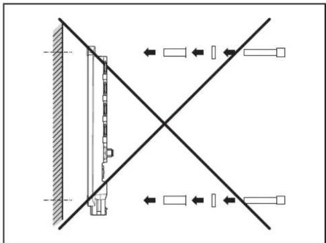
natural_image
Pure mechanical diagram showing a vertical beam and diagonal line intersecting, with no text or symbols present.Zone de raccordement
Eléments de service
Prise M12, 5 pôles, codage A (Con. 1...8, CAN OUT)

9.2 CR2041
CR2041
Module d'E/S
TOR et analogique
Profi I de communication
LED E/S 16 x LED orange
LED Power (PWR) LED verte
LED Mode (M) LED verte
LED d'application (A...D)
LED Lock (symbole de cadenas)
LED de diagnostic (DIA)
Affichage
Prise M12, 5 pôles, codage A (Con. 1...8, CAN OUT)

Prise M12, 5 pôles, codage A (Con. 1...8, CAN OUT)

The following error codes according to DSP-401 or DSP-301 are supported:
| EMCY code Error reg Additional code Description | |||
| 0x6100 0x11 0x00 "Internal Software | Overflow of an Rx queue e.g. frequency of the RxP-DOs is too high.Reset only externally via entry in the index 0x1003 Subldx 00." | ||
| 0x6101 0x11 0x00 "Internal Software | Overflow of an Tx queue e.g. device does not communicate with the bus.Reset only externally via entry in the index 0x1003 Subldx 00." | ||
| 0x8000 0x11 0x00 "Monitoring Sync Error | For communication cycle no sync object is received.Only in Operational. Reset with the next sync OBJ or PREOP" | ||
| 0x8100 0x11 0x00 Communication Err | |||
| 0x8131 0x11 0x00 "Monitoring Heart Beat Error | No guard object is received.Reset with the next Heart beat or PREOP" | ||
| 0x63xx 0x01 0x00 "Invalid parameter of an input or output.""xx"" means number of the IO-channel (00 ... 15)" | |||
| 0x5000 0x01 0x00 Memory Error | |||
| 0x3308 0x05 0x00 VBB2 error (only CR2041, CR2042) | |||
| 0x90xx 0x01 0x00 "Frequency input, Frequency too low""xx"" means number of the IO-channel (00 ... 15)" | |||
| 0x21xx 0x03 0x00 "Inputs, Openline""xx"" means number of the IO-channel (00 ... 15)" | |||
| 0x21xx 0x03 0x00 "Inputs, Short circuit""xx"" means number of the IO-channelCR2040 (00 ... 15) + 16; CR2042 (00 ... 07) + 8" | |||
| 0x21xx 0x03 0x00 "Inputs, Overcurrent""xx"" means number of the IO-channelCR2040 (00 ... 15) + 32; CR2042 (00 ... 07) + 16" | |||
| 0x23xx 0x03 0x00 "outputs, Openline""xx"" means number of the IO-channelCR2041 (00 ... 15); CR2042 (00 ... 07)" | |||
| 0x23xx 0x03 0x00 "outputs, Short circuit""xx"" means number of the IO-channelCR2041 (00 ... 15) + 16; CR2042 (00 ... 07) + 8" | |||
| 0x23xx 0x03 0x00 "outputs, Overload""xx"" means number of the IO-channelCR2041 (00 ... 15) + 32; CR2042 (00 ... 07) + 16" | |||
CANopen does not provide for two identical EMCY objects to be sent consecutively.
12.2 Object directory CR204x
Obligatory objects (index 0x1000...0x1FFF):
| Index S-idx Designation Data type Default Details | ||||||
| 0x1000 Device type ro UDINT 0x000F0 191 Device type | ||||||
| 0x1001 Error register ro USINT 0 Error register bitcoded to profile | 301Permissible values:0b0000 0000 = no error0b0000 0001 = generic error0b0001 0000 = communication error0b1000 0000 = manufacturer specific | |||||
| 0x1018 0x00 Device identification Number of entries | ro USINT 0x04 | Device identification | ||||
| 0x1003 0x00 Predefined error field Number of entries | rw | UDINT 0 An error list with 4 entries is supported | ||||
| 0x1005 | COB-ID | synchmessage | rw U | DINT 0x0000 | 0080 Identifier of | the synch messageBit 30 = 0 → device generates no synch messageBit 30 = 1 → device generates a synch messageBit 29 = 0 → 11 bit IDBit 29 = 1 → ID = 0x80 + node ID |
| 0x1006 | Communi-cation cycleperiod | rw U | DINT 0 Max. | time between 2 | synch objectsin [μs]Control resolution = 1 ms | |
| 0x1008 | Manufacturerdevice name | ro STRING CR204x Device designation (CR2040 orCR2041 or CR2042) | ||||
| 0x1009 | Manufacturerhardwareversion | ro STRING V00.00.00 Hardware version | ||||
| 0x100A | Manufacturersoftwareversion | ro STRING V00.00.00 Software version | ||||
| 0x1010 | 0x00 | Store para-metersLargestsub-indexsupported | ro USINT 0x01 | Number of "save options" | ||
| 0x01 | Save allparameters | rw U | DINT 2 Automatic saving of all parameterschanged0 = AutoSave OFF2 = AutoSave ON | |||
| 0x1011 | 0x00 | RestoredefaultparametersLargestsub-indexsupported | ro USINT 0x01 | Number of "restore options" | ||
| 0x01 | Restoreall defaultparameters | rw U | DINT 0x01 | If the String "load" is entered here,the default parameters set at thefactory are restored and becomevalid after the next reset. | ||
| 0x1014 | COBldEmergency | rw | UDINT | 0x80 + node ID | Bit 31 = 0 → EMCY is validBit 31 = 1 → EMCY is not validBit 29 = 0 → 11-bit IDBit 29 = 1 → ID = 0x80 + node IDCAN identifier can be changed bythe user. | |
| Index S-idx Designation Data type Default Details | |||||
| 0x1016 0x00 Con | sumer heartbeat times Nums consumer heartbeat time | ro USINT 0x01 Heartbeat monitoring time for the node Number of devices monitored = 1 | |||
| 0x01 Consumer heartbeat time | rw U DINT 0 Heartbeat monitoring time for the node Format: 0x0nntttt tttt = monitoring time [ms] nn = node number if nn=0 or tttt=0 → no monitoring | ||||
| 0x1017 Producer | heartbeat time | rw UI NT 0 Time interval [ms] during which the device generates a producer heartbeat | |||
12.2.1 Device-specific CR2040
Transmit PDO communication parameters (index 0x1800...0x18FF):
| Index S-idx Designation Data type Default Details | |||||
| 0x1800 0x00 TransmitPDO Com-municationParameterNumber ofentries | ro USINT 0x05 Configuration transmit PDO 1number of entries = 5 | ||||
| 0x01 COBID usedby PDO | rw U | DINT 0x180 | +Node ID | CAN ID of the transmit PDO 1Bit 31 = 0 → PDO is validBit 31 = 1 → PDO is not valid | |
| 0x02 transmissiontype | rw USINT 0xFF | 0x00 = synch acyclic | 0x01...0xF0 = synch cyclic; valuesare only transmitted after „n" synchobjectsn = 1...240 = 0x01...0xF00xFC/0xFD not implemented0xFE = asynch man. spec. event;values are immediately transferred0xFF = asynch device profile event;values are immediately transferred | ||
| 0x03 inhibit time rw UINT | 0 | delay time in the transmissiontype "asynch" before the PDO istransmitted again at the earliest.(0...65535 • 100 μs) | |||
| 0x04 reserved rw USINT 0 | reserve | ||||
| 0x05 | event time | rw | UINT | 0 | |
| 0x1801 0x00 TransmitPDO Com-municationParameterNumber ofentries | ro USINT 0x05 Configuration transmit PDO 2number of entries = 5 | ||||
| 0x01 COBID usedby PDO | rw U | DINT 0x280 | +Node ID | CAN ID of the transmit PDO 2Bit 31 = 0 → PDO is validBit 31 = 1 → PDO is not valid | |
| 0x02 transmissiontype | rw USINT 0x01 | 0x00 = synch acyclic | 0x01...0xF0 = synch cyclic; valuesare only transmitted after „n" synchobjectsn = 1...240 = 0x01...0xF00xFC/0xFD not implemented0xFE = asynch man. spec. event;values are immediately transferred0xFF = asynch device profile event;values are immediately transferred | ||
| 0x03 inhibit time rw UINT 0 delay time in the transmissiontype "asynch" before the PDO istransmitted again at the earliest.(0...65535 • 100 μs) | |||||
| 0x04 reserved rw USINT 0 reserve | |||||
| 0x05 event timewUINT 0 max. transfer break in thetransmissi-on type „asynch" (0...65535 ms)When this time has elapsed, the PDOis transferred even if the appl. eventhas not accured. | |||||
| 0x1802 0x00 TransmitPDO Com-municationParameterNumber ofentries | ro USINT 0x05 Configuration transmit PDO 3number of entries = 5 | ||||
| 0x01 COBID usedby PDO | rw U | DINT 0x380 | +Node ID | CAN ID of the transmit PDO 3Bit 31 = 0 → PDO is validBit 31 = 1 → PDO is not valid | |
| 0x02 transmissiontype | rw USINT 0x01 | 0x00 = synch acyclic | 0x01...0xF0 = synch cyclic; valuesare only transmitted after „n" synchobjectsn = 1...240 = 0x01...0xF00xFC/0xFD not implemented0xFE = asynch man. spec. event;values are immediately transferred0xFF = asynch device profile event;values are immediately transferred | ||
| 0x03 inhibit time rw UINT 0 delay time in the transmissiontype "asynch" before the PDO istransmitted again at the earliest.(0...65535 • 100 μs) | |||||
| 0x04 reserved rw USINT 0 reserve | |||||
| 0x05 event timewUINT 0 max. transfer break in thetransmissi-on type „asynch" (0...65535 ms)When this time has elapsed, the PDOis transferred even if the appl. eventhas not accured. | |||||
| 0x1803 0x00 TransmitPDO Com-municationParameterNumber ofentries | ro USINT 0x05 Configuration transmit PDO 4number of entries = 5 | ||||
| 0x01 COBID usedby PDO | rw U DINT 0x480 +Node ID | CAN ID of the transmit PDO 4Bit 31 = 0 → PDO is validBit 31 = 1 → PDO is not valid | |||
| 0x02 transmissiontype | rw USINT 0x01 0x00 = synch acyclic0x01...0xF0 = synch cyclic; valuesare only transmitted after „n" synchobjectsn = 1...240 = 0x01...0xF00xFC/0xFD not implemented0xFE = asynch man. spec. event;values are immediately transferred0xFF = asynch device profile event;values are immediately transferred | ||||
| 0x03 inhibit time rw UINT 0 delay time in the transmissiontype "asynch" before the PDO istransmitted again at the earliest.(0...65535 • 100 μs) | |||||
| 0x04 reserved rw USINT 0 reserve | |||||
| 0x05 event timewrUINT 0 max. transfer break in thetransmissi-on type „asynch" (0...65535 ms)When this time has elapsed, the PDOis transferred even if the appl. eventhas not accured. | |||||
| 0x1804 0x00 TransmitPDO Com-municationParameterNumber ofentries | ro USINT 0x05 Configuration transmit PDO 5number of entries = 5 | ||||
| 0x01 COBID usedby PDO | rw U DINT 0x181 +Node ID | CAN ID of the transmit PDO 5Bit 31 = 0 → PDO is validBit 31 = 1 → PDO is not valid | |||
| 0x02 transmissiontype | rw USINT 0x01 0x00 = synch acyclic0x01...0xF0 = synch cyclic; valuesare only transmitted after „n" synchobjectsn = 1...240 = 0x01...0xF00xFC/0xFD not implemented0xFE = asynch man. spec. event;values are immediately transferred0xFF = asynch device profile event;values are immediately transferred | ||||
| 0x03 inhibit time rw UINT 0 delay time in the transmissiontype "asynch" before the PDO istransmitted again at the earliest.(0...65535 • 100 μs) | |||||
| 0x04 reserved rw USINT 0 reserve | |||||
| 0x05 event timewrUINT 0 max. transfer break in thetransmissi-on type „asynch" (0...65535 ms)When this time has elapsed, the PDOis transferred even if the appl. eventhas not accured. | |||||
| 0x1805 0x00 TransmitPDO Com-municationParameterNumber ofentries | ro USINT 0x05 Configuration transmit PDO 6number of entries = 5 | ||||
| 0x01 COBID usedby PDO | rw U | DINT 0x281 | +Node ID | CAN ID of the transmit PDO 6Bit 31 = 0 → PDO is validBit 31 = 1 → PDO is not valid | |
| 0x02 transmissiontype | rw USINT 0x01 | 0x00 = synch acyclic | 0x01...0xF0 = synch cyclic; valuesare only transmitted after „n" synchobjectsn = 1...240 = 0x01...0xF00xFC/0xFD not implemented0xFE = asynch man. spec. event;values are immediately transferred0xFF = asynch device profile event;values are immediately transferred | ||
| 0x03 inhibit time rw UINT 0 delay time in the transmissiontype "asynch" before the PDO istransmitted again at the earliest.(0...65535 • 100 μs) | |||||
| 0x04 reserved rw USINT 0 reserve | |||||
| 0x05 event timewUINT 0 max. transfer break in thetransmissi-on type „asynch" (0...65535 ms)When this time has elapsed, the PDOis transferred even if the appl. eventhas not accured. | |||||
| 0x1806 0x00 TransmitPDO Com-municationParameterNumber ofentries | ro USINT 0x05 Configuration transmit PDO 7number of entries = 5 | ||||
| 0x01 COBID usedby PDO | rw U | DINT 0x381 | +Node ID | CAN ID of the transmit PDO 7Bit 31 = 0 → PDO is validBit 31 = 1 → PDO is not valid | |
| 0x02 transmissiontype | rw USINT 0x01 | 0x00 = synch acyclic | 0x01...0xF0 = synch cyclic; valuesare only transmitted after „n" synchobjectsn = 1...240 = 0x01...0xF00xFC/0xFD not implemented0xFE = asynch man. spec. event;values are immediately transferred0xFF = asynch device profile event;values are immediately transferred | ||
| 0x03 inhibit time rw UINT 0 delay time in the transmissiontype "asynch" before the PDO istransmitted again at the earliest.(0...65535 • 100 μs) | |||||
| 0x04 reserved rw USINT 0 reserve | |||||
| 0x05 event timewUINT 0 max. transfer break in thetransmissi-on type „asynch" (0...65535 ms)When this time has elapsed, the PDOis transferred even if the appl. eventhas not accured. | |||||
| 0x1807 0x00 TransmitPDO Com-municationParameterNumber ofentries | ro USINT 0x05 Configuration transmit PDO 8number of entries = 5 | ||||
| 0x01 COBID usedby PDO | rw U DINT 0x481 +Node ID | CAN ID of the transmit PDO 8Bit 31 = 0 → PDO is validBit 31 = 1 → PDO is not valid | |||
| 0x02 transmissiontype | rw USINT 0x01 0x00 = synch acyclic0x01...0xF0 = synch cyclic; valuesare only transmitted after „n" synchobjectsn = 1...240 = 0x01...0xF00xFC/0xFD not implemented0xFE = asynch man. spec. event;values are immediately transferred0xFF = asynch device profile event;values are immediately transferred | ||||
| 0x03 inhibit time rw UINT 0 delay time in the transmissiontype "asynch" before the PDO istransmitted again at the earliest.(0...65535 • 100 μs) | |||||
| 0x04 reserved rw USINT 0 reserve | |||||
| 0x05 event timewrUINT 0 max. transfer break in thetransmissi-on type „asynch" (0...65535 ms)When this time has elapsed, the PDOis transferred even if the appl. eventhas not accured. | |||||
| 0x1808 0x00 TransmitPDO Com-municationParameterNumber ofentries | ro USINT 0x05 Configuration transmit PDO 9number of entries = 5 | ||||
| 0x01 COBID usedby PDO | rw U DINT 0x182 +Node ID | CAN ID of the transmit PDO 9Bit 31 = 0 → PDO is validBit 31 = 1 → PDO is not valid | |||
| 0x02 transmissiontype | rw USINT 0x01 0x00 = synch acyclic0x01...0xF0 = synch cyclic; valuesare only transmitted after „n" synchobjectsn = 1...240 = 0x01...0xF00xFC/0xFD not implemented0xFE = asynch man. spec. event;values are immediately transferred0xFF = asynch device profile event;values are immediately transferred | ||||
| 0x03 inhibit time rw UINT 0 delay time in the transmissiontype "asynch" before the PDO istransmitted again at the earliest.(0...65535 • 100 μs) | |||||
| 0x04 reserved rw USINT 0 reserve | |||||
| 0x05 event timewrUINT 0 max. transfer break in thetransmissi-on type „asynch" (0...65535 ms)When this time has elapsed, the PDOis transferred even if the appl. eventhas not accured. | |||||
| 0x1809 0x00 TransmitPDO Com-municationParameterNumber ofentries | ro USINT 0x05 Configuration transmit PDO 10number of entries = 5 | ||||
| 0x01 COBID usedby PDO | rw U DINT 0x282 +Node ID | CAN ID of the transmit PDO 10Bit 31 = 0 → PDO is validBit 31 = 1 → PDO is not valid | |||
| 0x02 transmissiontype | rw USINT 0x01 0x00 = synch acyclic0x01...0xF0 = synch cyclic; valuesare only transmitted after „n" synchobjectsn = 1...240 = 0x01...0xF00xFC/0xFD not implemented0xFE = asynch man. spec. event;values are immediately transferred0xFF = asynch device profile event;values are immediately transferred | ||||
| 0x03 inhibit time rw UINT 0 delay time in the transmissiontype "asynch" before the PDO istransmitted again at the earliest.(0...65535 • 100 μs) | |||||
| 0x04 reserved rw USINT 0 reserve | |||||
| 0x05 event timewUINT 0 max. transfer break in thetransmissi-on type „asynch" (0...65535 ms)When this time has elapsed, the PDOis transferred even if the appl. eventhas not accured. | |||||
Transmit PDO mapping (index 0x1A00...0x1AFF):
| Index S-idx Designation Data type Default Details | |||||
| 0x1A00 0x00 TransmitPDO mappingNumber ofmappedobjects inPDO | rw U | SINT 0x07 | mapping transmit | PDO 1number of integrated applicationobjects = 7 | |
| 0x01 P | DO mapping | rw U | DINT 0x6000 | 0108 Index 0x6000, SubIndex 0x01binary inputs 00...07: actual values(bit coded) | |
| 0x02 P | DO mapping | rw U | DINT 0x6000 | 0208 Index 0x6000, SubIndex 0x02binary inputs 08...15: actual values(bit coded) | |
| 0x03 P | DO mapping | rw U | DINT 0x2020 | 0108 Index 0x2020, SubIndex 0x01binary inputs 00...07: flag "shortcircuit" (bit coded) | |
| 0x04 P | DO mapping | rw U | DINT 0x2020 | 0208 Index 0x2020, SubIndex 0x02binary inputs 08...15: flag "shortcircuit" (bit coded) | |
| 0x05 P | DO mapping | rw U | DINT 0x2021 | 0108 Index 0x2021, SubIndex 0x01outputs 00...07: flag " wire break " (bitcoded) | |
| 0x06 P | DO mapping | rw U | DINT 0x2021 | 0208 Index 0x2021, SubIndex 0x02outputs 08...15: flag " wire break "(bit coded) | |
| 0x07 P | DO mapping | rw U | DINT 0x2025 | 0108 Index 0x2025, SubIndex 0x01inputs 00...03: flag " overload " (bitcoded) | |
| 0x1A01 | 0x00 Transmit | PDO mappingNumber ofmappedobjects inPDO | rw USINT 0x04 | mapping transmit | PDO 2 (analogueinputs)number of integrated applicationobjects = 4 |
| 0x01 P | DO mapping | rw UDINT 0x640 | 4 0110 Index 0x6 | 404, SubIndex 0x01analogue input 00: actual value(depending on the configuration0x2000) | |
| 0x02 P | DO mapping | rw UDINT 0x640 | 4 0210 Index 0x6 | 404, SubIndex 0x02analogue input 01: actual value(depending on the configuration0x2000)) | |
| 0x03 P | DO mapping | rw UDINT 0x640 | 4 0310 Index 0x6 | 404, SubIndex 0x03analogue input 02: actual value(depending on the configuration0x2000) | |
| 0x04 P | DO mapping | rw UDINT 0x640 | 4 0410 Index 0x6 | 404, SubIndex 0x04analogue input 03: actual value(depending on the configuration0x2000) | |
| 0x1A02 | 0x00 Transmit | PDO mappingNumber ofmappedobjects inPDO | rw USINT 0x04 | mapping transmit | PDO 3 (analogueinputs)number of integrated applicationobjects = 4 |
| 0x01 P | DO mapping | rw UDINT 0x640 | 4 0510 Index 0x6 | 404, SubIndex 0x05analogue input 04: actual value(depending on the configuration0x2000) | |
| 0x02 P | DO mapping | rw UDINT 0x640 | 4 0610 Index 0x6 | 404, SubIndex 0x06analogue input 05: actual value(depending on the configuration0x2000)) | |
| 0x03 P | DO mapping | rw UDINT 0x640 | 4 0710 Index 0x6 | 404, SubIndex 0x07analogue input 06: actual value(depending on the configuration0x2000) | |
| 0x04 P | DO mapping | rw UDINT 0x640 | 4 0810 Index 0x6 | 404, SubIndex 0x08analogue input 07: actual value(depending on the configuration0x2000) | |
| 0x1A03 0x00 TransmitPDO mappingNumber ofmappedobjects inPDO | rw USINT 0x04 mapping transmit | PDO 4number of integrated applicationobjects = 4 | |||
| 0x01 PDO mapping | rw UDINT 0x2030 0110 Index 0x2030, SubIndex 0x01input 08: actual resistor value | ||||
| 0x02 PDO mapping | rw UDINT 0x2030 0210 Index 0x2030, SubIndex 0x02input 10: actual resistor value | ||||
| 0x03 PDO mapping | rw UDINT 0x2030 0310 Index 0x2030, SubIndex 0x03input 12: actual resistor value | ||||
| 0x04 PDO mapping | rw UDINT 0x2030 0410 Index 0x2030, SubIndex 0x04input 14: actual resistor value | ||||
| 0x1A04 0x00 TransmitPDO mappingNumber ofmappedobjects inPDO | rw USINT 0x02 mapping transmit | PDO 5 (periodetime IN09, IN11)number of integrated applicationobjects = 2 | |||
| 0x01 PDO mapping | rw UDINT 0x2012 0120 Index 0x2012, SubIndex 0x01frequency input IN09: periode time ofthe signal | ||||
| 0x02 PDO mapping | rw UDINT 0x2012 0220 Index 0x2012, SubIndex 0x02frequency input IN11: periode time ofthe signal | ||||
| 0x1A05 0x00 TransmitPDO mappingNumber ofmappedobjects inPDO | rw USINT 0x02 mapping transmit | PDO 6 (periodetime IN13, IN15)number of integrated applicationobjects = 2 | |||
| 0x01 PDO mapping | rw UDINT 0x2012 0320 Index 0x2012, SubIndex 0x03frequency input IN13: periode time ofthe signal | ||||
| 0x02 PDO mapping | rw UDINT 0x2012 0420 Index 0x2012, SubIndex 0x04frequency input IN15: periode time ofthe signal | ||||
| Index S-idx Designation Data type Default Details | ||||||
| 0x1A06 | 0x00 Transmit | PDO mappingNumber ofmappedobjects inPDO | rw U | SINT 0x04 | mapping transmit | PDO 7 (duty cycleof the signal on the frequency inputIN09, IN11, IN13, IN15)number of integrated applicationobjects = 4 |
| 0x01 P | DO mapping | rw U | DINT 0x201 | 4 0110 Index 0x2 | 2014, SubIndex 0x01frequency input IN09: duty cycle ofthe signal in %o | |
| 0x02 P | DO mapping | rw U | DINT 0x201 | 4 0210 Index 0x2 | 2014, SubIndex 0x02frequency input IN11: duty cycle ofthe signal in %o | |
| 0x03 P | DO mapping | rw U | DINT 0x201 | 4 0310 Index 0x2 | 2014, SubIndex 0x03frequency input IN13: duty cycle ofthe signal in %o | |
| 0x04 P | DO mapping | rw U | DINT 0x201 | 4 0410 Index 0x2 | 2014, SubIndex 0x04frequency input IN15: duty cycle ofthe signal in %o | |
| 0x1A07 | 0x00 Transmit | PDO mappingNumber ofmappedobjects inPDO | rw U | SINT 0x02 | mapping transmit | PDO 8 (frequencyon IN09, IN11)number of integrated applicationobjects = 2 |
| 0x01 P | DO mapping | rw U | DINT 0x201 | 5 0120 Index 0x2 | 2015, SubIndex 0x01frequency input IN09: frequencyvalue of the signal in Hz | |
| 0x02 P | DO mapping | rw U | DINT 0x201 | 5 0220 Index 0x2 | 2015, SubIndex 0x02frequency input IN11: frequency valueof the signal in Hz | |
| 0x1A08 | 0x00 Transmit | PDO mappingNumber ofmappedobjects inPDO | rw U | SINT 0x02 | mapping transmit | PDO 9 (frequencyon IN13, IN15)number of integrated applicationobjects = 2 |
| 0x01 P | DO mapping | rw U | DINT 0x201 | 5 0320 Index 0x2 | 2015, SubIndex 0x03frequency input IN13: frequencyvalue of the signal in Hz | |
| 0x02 P | DO mapping | rw U | DINT 0x201 | 5 0420 Index 0x2 | 2015, SubIndex 0x04frequency input IN15: frequencyvalue of the signal in Hz | |
| Index S-idx Designation Data type Default Details | ||||||
| 0x1A09 0x00 TransmitPDO mappingNumber ofmappedobjects inPDO | rw U | SINT 0x02 | mapping transmit | PDO 10 (system flag)number of integrated application objects = 2 | ||
Manufacturer-specific objekts (index 0x2000...0x6FFF):
| Index S-idx Designation Data type Default Details | ||||||
| 0x2000 0x00 IO configuration Largest sub-index supported | ro USINT 16 Configuration inputs/outputs largest supported Sub-index = 32 | |||||
| 0x01 Configuration IN00 | rw USINT 10 0 = 0x00 | 3 = 0x036 = 0x067 = 0x079 = 0x0910 = 0x0A11 = 0x0B12 = 0x0C | off Input IN000...10 000 mV ratiometric 0...1000 %00...20 000 μA0...32 000 mV binary plus switched binary plus switched with diagnosis binary minus switched | |||
| 0x02 Configuration IN01 | rw USINT 10 0 = 0x00 | 3 = 0x036 = 0x067 = 0x079 = 0x0910 = 0x0A11 = 0x0B12 = 0x0C | off Input IN010...10 000 mV ratiometric 0...1000 %00...20 000 μA0...32 000 mV binary plus switched binary plus switched with diagnosis binary minus switched | |||
| 0x03 Configuration IN02 | rw USINT 10 0 = 0x00 | 3 = 0x036 = 0x067 = 0x079 = 0x0910 = 0x0A11 = 0x0B12 = 0x0C | off Input IN020...10 000 mV ratiometric 0...1000 %00...20 000 μA0...32 000 mV binary plus switched binary plus switched with diagnosis binary minus switched | |||
| 0x2000 0x04 Configuration IN03 | rw USINT 10 0 = 0x00 | 3 = 0x036 = 0x067 = 0x079 = 0x0910 = 0x0A11 = 0x0B12 = 0x0C | off Input IN030...10 000 mVratiometric 0...1000 %o0...20 000 μA0...32 000 mVbinary plus switchedbinary plus switchedwith diagnosisbinary minus switched | |||
| Index S-idx Designation Data type Default Details | |||||||
| 0x2000 0x0A Configuration IN09 | rw USINT 01 0 = 0x00 | 01 = 0x0114 = 0x0E20 = 0x14 | off Input IN09binary plus switched frequency0...30 000 Hzperiod duration | ||||
| 0x0B Configuration IN10 | rw USINT 10 0 = 0x00 | 10 = 0x0A11 = 0x0B18 = 0x12 | off Input IN10binary plus switched binary plus switched with diagnosis16...30 000 Ohm | ||||
| 0x0C Configuration IN11 | rw USINT 01 0 = 0x00 | 01 = 0x0114 = 0x0E20 = 0x14 | off Input IN11binary plus switched frequency0...30 000 Hzperiod duration | ||||
| 0x0D Configuration IN12 | rw USINT 10 0 = 0x00 | 10 = 0x0A11 = 0x0B18 = 0x12 | off Input IN12binary plus switched binary plus switched with diagnosis16...30 000 Ohm | ||||
| 0x0E Configuration IN13 | rw USINT 01 0 = 0x00 | 01 = 0x0114 = 0x0E20 = 0x14 | off Input IN12binary plus switched frequency0...30 000 Hzperiod duration | ||||
| 0x0F Configuration IN14 | rw USINT 10 0 = 0x00 | 10 = 0x0A11 = 0x0B18 = 0x12 | off Input IN14binary plus switched binary plus switched with diagnosis16...30 000 Ohm | ||||
| 0x10 Configuration IN15 | rw USINT 01 0 = 0x00 | 01 = 0x0114 = 0x0E20 = 0x14 | off Input IN15binary plus switched frequency0...30 000 Hzperiod duration | ||||
| 0x2012 0x00 Period input ro USINT 4 | Largest sub-index supported | ||||||
| 0x01 Period duration IN09 | ro | UDINT | 0 | IN09 period duration [μs] | |||
| 0x02 Period duration IN11 | ro | UDINT | 0 | IN11 period duration [μs] | |||
| 0x03 Period duration IN13 | ro | UDINT | 0 | IN13 period duration [μs] | |||
| 0x04 Period duration IN15 | ro | UDINT | 0 | IN15 period duration [μs] | |||
| Index S-idx Designation Data type Default Details | ||||||
| 0x2013 0x00 Period input number of periods for average | ro USINT 4 Largest sub-index supported | |||||
| 0x01 Number of periods IN09 | rw USINT 4 1...255 IN09 number of | periods | ||||
| 0x02 Number of periods IN11 | rw USINT 4 1...255 IN11 number of | periods | ||||
| 0x03 Number of periods IN13 | rw USINT 4 1...255 IN13 number of | periods | ||||
| 0x04 Number of periods IN15 | rw USINT 4 1...255 IN15 number of | periods | ||||
| 0x2014 0x00 Period input - ratio value | ro USINT 4 Largest sub-index supported | |||||
| 0x01 Period ratio value IN09 | ro UI NT 0 0...1 000 IN09 marc-to-space | ratio [%] | ||||
| 0x02 Period ratio value IN11 | ro UI NT 0 0...1 000 IN11 marc-to-space | ratio [%] | ||||
| 0x03 Period ratio value IN13 | ro UI NT 0 0...1 000 IN13 marc-to-space | ratio [%] | ||||
| 0x04 Period ratio value IN15 | ro UI NT 0 0...1 000 IN15 marc-to-space | ratio [%] | ||||
| 0x2015 0x00 Frequency input | ro USINT 4 Largest sub-index supported | |||||
| 0x01 Frequency IN09 | ro REAL 1 0...30 000 IN09 frequency [Hz] | |||||
| 0x02 Frequency IN11 | ro REAL 1 0...30 000 IN11 frequency [Hz] | |||||
| 0x03 Frequency IN13 | ro REAL 1 0...30 000 IN13 frequency [Hz] | |||||
| 0x04 Frequency IN15 | ro REAL 1 0...30 000 IN15 frequency [Hz] | |||||
| 0x2016 0x00 Timebase ro USINT 4 Largest sub-index supported | ||||||
| Index S-idx Designation Data type Default Details | |||||||
| 0x2020 0x00 Input - short to supply voltage | ro USINT 2 Largest sub-index supported | ||||||
| 0x2021 0x00 Input - wire break | ro USINT 2 Largest sub-index supported | ||||||
| 0x01 Wire breakIN00...IN07 | ro USINT 0 0 = normal | 1 = wire break | channels (bit coded)0b---- ---X = IN000b---- --X- = IN010b---- -X-- = IN020b---- X--- = IN030b----X ---- = IN040b--X- ---- = IN050b-X-- ---- = IN060bX--- ---- = IN07 | ||||
| 0x2025 0x00 Input analog - overcurrent | ro USINT 1 Largest sub-index supported | ||||||
| Index S-idx Designation Data type Default Details | |||||||
| 0x2030 0x00 Input resistor ro USINT 4 Largest sub-index supported | |||||||
| 0x2040 0x00 System supply voltage VBBS | ro USINT 1 Largest sub-index supported | ||||||
| node ID[!] value(0x20F0) !=value(20F1) | |||||||
| node ID[!] value(0x2F0) !=value(20F1) | |||||||
| node ID[!] value(0x20F0) !=value(20F1) | |||||||
| Index S-idx Designation Data type Default Details | |||||
| 0x6000 0x00 Binary input Largest sub-index supported | ro USINT 0x02 Binary inputs IN00...IN07 | Largest supported sub-index = 2 | |||
| 0x01 Binary inputs IN00 - IN07 | ro USINT 0 Binary inputs IN00...IN07 | ||||
| 0x02 Binary inputs IN08 - IN15 | ro USINT 0 Binary inputs IN08...IN15 | ||||
| 0x6404 0x00 Analogue input Largest sub-index supported | ro USINT 0x08 Analogue inputs IN08...IN15 | Largest supported sub-index = 4 | |||
| 0x01 Analogue input IN00 | ro UINT -- Analogue value of input IN00 | ||||
| 0x02 Analogue input IN01 | ro UINT -- Analogue value of input IN01 | ||||
| 0x03 Analogue input IN02 | ro UINT -- Analogue value of input IN02 | ||||
| 0x04 Analogue input IN03 | ro UINT -- Analogue value of input IN03 | ||||
| 0x05 Analogue input IN04 | ro UINT -- Analogue value of input IN04 | ||||
| 0x06 Analogue input IN05 | ro UINT -- Analogue value of input IN05 | ||||
| 0x07 Analogue input IN06 | ro UINT -- Analogue value of input IN06 | ||||
| 0x08 Analogue input IN07 | ro UINT -- Analogue value of input IN07 | ||||
12.2.2 Device-specific CR2041
Receive PDO communication parameters (index 0x1400...0x14FF):
| Index S-idx Designation Data type Default Details | |||||
| 0x1400 0x00 Receive PDOCommunication Parameter Number of entries | ro USINT 0x02Receive PDO 1: binary outputs 0 - 15number of entries = 2 | ||||
| 0x01 COBID used by PDO | rw UDINT 0x200+ node ID | CAN ID of the first read PDOBit 31 = 0 → PDO is validBit 31 = 1 → PDO is not valid | |||
| 0x02 transmission type | rw USINT 0x01 0x00 = synch acyclic | 0x01...0xF0 = synch cyclic; outputs are only updated after „n" synch objectsn = 1...240 = 0x01...0xF00xFC/0xFD not implemented0xFE = asynch man. spec. event; outputs are updated immediately0xFF = asynch device profile event; outputs are updated immediately | |||
| 0x1401 0x00 Receive PDOCommunication Parameter Number of entries | ro USINT 0x02Receive PDO 2: PWM outputs 0 - 3number of entries = 2 | ||||
| 0x01 COBID used by PDO | rw UDINT 0x300+ node ID | CAN ID of the second read PDOBit 31 = 0 → PDO is validBit 31 = 1 → PDO is not valid | |||
| 0x02 transmission type | rw USINT 0x01 0x00 = synch acyclic | 0x01...0xF0 = synch cyclic; outputs are only updated after „n" synch objectsn = 1...240 = 0x01...0xF00xFC/0xFD not implemented0xFE = asynch man. spec. event; outputs are updated immediately0xFF = asynch device profile event; outputs are updated immediately | |||
| 0x1402 0x00 Receive PDO Communication Parameter Number of entries | ro USINT 0x02Receive PDO 3: PWM outputs 4 - 7 number of entries = 2 | ||||
| 0x01 COBID used by PDO | rw U | DINT 0x400 | + node ID | CAN-ID of the 3. read PDO Bit 31 = 0 → PDO is valid Bit 31 = 1 → PDO is not valid | |
| 0x02 transmission type | rw USINT 0x01 | 0x00 = synch acyclic | 0x01...0xF0 = synch cyclic; outputs are only updated after „n" synch objects n = 1...240 = 0x01...0xF0 0xFC/0xFD not implemented 0xFE = asynch man. spec. event; outputs are updated immediately 0xFF = asynch device profile event; outputs are updated immediately | ||
| 0x1403 0x00 Receive PDO Communication Parameter Number of entries | ro USINT 0x02Receive PDO 4: PWM outputs 8 - 11 number of entries = 2 | ||||
| 0x01 COBID used by PDO | rw U | DINT 0x500 | + node ID | CAN-ID of the 3. read PDO Bit 31 = 0 → PDO is valid Bit 31 = 1 → PDO is not valid | |
| 0x02 transmission type | rw USINT 0x01 | 0x00 = synch acyclic | 0x01...0xF0 = synch cyclic; outputs are only updated after „n" synch objects n = 1... 240 = 0x01...0xF0 0xFC/0xFD not implemented 0xFE = asynch man. spec. event; outputs are updated immediately 0xFF = asynch device profile event; outputs are updated immediately | ||
| 0x1404 0x00 Receive PDO Communication Parameter Number of entries | ro USINT 0x02 | Receive PDO 5: PWM outputs 12 - 15 number of entries = 2 | |||
| 0x01 OBID used by PDO | rw U | DINT 0x201 | + node ID | CAN-ID of the 3. read PDO Bit 31 = 0 → PDO is valid Bit 31 = 1 → PDO is not valid | |
| 0x02 transmission type | rw USINT 0x01 | 0x00 = synch acyclic | 0x01...0xF0 = synch cyclic; outputs are only updated after „n" synch objects n = 1...240 = 0x01...0xF0 0xFC/0xFD not implemented 0xFE = asynch man. spec. event; outputs are updated immediately 0xFF = asynch device profile event; outputs are updated immediately | ||
Receive PDO mapping (index 0x1600...0x16FF):
| Index S-idx Designation Data type Default Details | |||||
| 0x1600 0x00 Receive PDO mapping Number of mapped objects in PDO | rw U | SINT 0x02 | Mapping read PDO | DO 1: binary outputs number of integrated application objects = 2 | |
| ro UDINT 0x6200 0108 1 byte in index 0x6200, SubIndex 01 Binary outputs OUT00...OUT07 0b---- ---X = OUT00 0b---- --X- = OUT01 0b---- -X-- = OUT02 0b---- X--- = OUT03 0b----X ---- = OUT04 0b--X- ---- = OUT05 0b-X-- ---- = OUT06 0bX--- ---- = OUT07 | |||||
| ro UDINT 0x6200 0208 1 byte in index 0x6200, SubIndex 02 Binary outputs OUT08...OUT15 0b---- ---X = OUT08 0b---- --X- = OUT09 0b---- -X-- = OUT10 0b---- X--- = OUT11 0b----X ---- = OUT12 0b--X- ---- = OUT13 0b-X-- ---- = OUT14 0bX--- ---- = OUT15 | |||||
| 0x1601 0x00 Receive PDO mapping Number of mapped objects in PDO | rw U | SINT 0x04 | Mapping read PDO | DO 2: PWM outputs OUT00...OUT03 number of integrated application objects = 4 | |
| 0x01 P | DO map-ping | rw U | DINT 0x641 | 4 0110 PWM/current output OUT00 Index 0x6414, SubIndex 0x01 contains the preset value of the PWM output OUT00, the value is interpreted as duty cycle in ‰ or as target current value (depending on the configuration index 0x2000) | |
| 0x02 P | DO map-ping | rw U | DINT 0x641 | 4 0210 PWM/ current output OUT01 Index 0x6414, SubIndex 0x02 contains the preset value of the PWM output OUT01, the value is interpreted as duty cycle in ‰ or as target current value (depending on the configuration index 0x2000) | |
| 0x03 P | DO map-ping | rw U | DINT 0x641 | 4 0310 PWM/ current output OUT02 Index 0x6414, SubIndex 0x03 contains the preset value of the PWM output OUT02, the value is interpreted as duty cycle in ‰ or as target current value (depending on the configuration index 0x2000) | |
| 0x04 P | DO map-ping | rw U | DINT 0x641 | 4 0410 PWM/ current output OUT03 Index 0x6414, SubIndex 0x04 contains the preset value of the PWM output OUT03, the value is interpreted as duty cycle in ‰ or as target current value (depending on the configuration index 0x2000) | |
| 0x1602 0x00 "ReceivePDO mappingNumber ofmappedobjects inPDO" | rw U | SINT 0x04 | Mapping read PDO | DO 3:PWM outputs OUT04...OUT07number of integrated applicationobjects = 4 | |
| 0x01 PDO mapping | |||||
| 0x02 PDO mapping | |||||
| 0x03 PDO mapping | |||||
| 0x04 PDO mapping | |||||
| 0x1603 0x00 Receive PDO mapping Number of mapped objects in PDO | rw U | SINT 0x04 | Mapping read PDO | DO 4: PWM outputs OUT08...OUT11 number of integrated application objects = 4 | |
| 0x01 P | DO map-ping | rw U | DINT 0x6414 0910 PWM/ current output OUT08 Index 0x6414, SubIndex 0x09 contains the preset value of the PWM output OUT08, the value is interpreted as duty cycle in ‰ or as target current value (depending on the configuration index 0x2000) | ||
| 0x02 P | DO map-ping | rw U | DINT 0x6414 0A10 PWM/ current output OUT09 Index 0x6414, SubIndex 0x0A contains the preset value of the PWM output OUT09, the value is interpreted as duty cycle in ‰ or as target current value (depending on the configuration index 0x2000) | ||
| 0x03 P | DO map-ping | rw U | DINT 0x6414 0B10 PWM/ current output OUT10 Index 0x6414, SubIndex 0x0B contains the preset value of the PWM output OUT10, the value is interpreted as duty cycle in ‰ or as target current value (depending on the configuration index 0x2000) | ||
| 0x04 P | DO map-ping | rw U | DINT 0x6414 0C10 PWM/ current output OUT11 Index 0x6414, SubIndex 0x0C contains the preset value of the PWM output OUT11, the value is interpreted as duty cycle in ‰ or as target current value (depending on the configuration index 0x2000) | ||
| Index S- | dx Designation Data type Default Details | |||||
| 0x1604 | 0x00 Receive PDO mapping Number of mapped objects in PDO | rw U | SINT 0x04 | Mapping read PDO | DO 5:PWM outputs OUT12...OUT15 number of integrated application objects = 4 | |
| 0x01 P | DO map-ping | rw U | DINT 0x641 | 4 0D10 PWM/ current output OUT12Index 0x6414, SubIndex 0x0D contains the preset value of the PWM output OUT12, the value is interpreted as duty cycle in ‰ or as target current value (depending on the configuration index 0x2000) | ||
| 0x02 P | DO map-ping | rw U | DINT 0x641 | 4 0E10 PWM/ current output OUT13Index 0x6414, SubIndex 0x0E contains the preset value of the PWM output OUT13, the value is interpreted as duty cycle in ‰ or as target current value (depending on the configuration index 0x2000) | ||
| 0x03 P | DO map-ping | rw U | DINT 0x641 | 4 0F10 PWM/ current output OUT14Index 0x6414, SubIndex 0x0F contains the preset value of the PWM output OUT14, the value is interpreted as duty cycle in ‰ or as target current value (depending on the configuration index 0x2000) | ||
| 0x04 P | DO map-ping | rw U | DINT 0x641 | 4 1010 PWM/ current output OUT15Index 0x6414, SubIndex 0x10 contains the preset value of the PWM output OUT15, the value is interpreted as duty cycle in ‰ or as target current value (depending on the configuration index 0x2000) | ||
Transmit PDO communication parameters (index 0x1800...0x18FF):
| Index S-idx Designation Data type Default Details | |||||
| 0x1800 0x00 TransmitPDO Com-municationParameterNumber ofentries | ro USINT 0x05 Configuration transmit PDO 1number of entries = 5 | ||||
| 0x01 COBID usedby PDO | rw UDINT 0x180 +Node ID | CAN ID of the transmit PDO 1Bit 31 = 0 → PDO is validBit 31 = 1 → PDO is not valid | |||
| 0x02 transmissiontype | rw USINT 0x01 0x00 = synch acyclic0x01...0xF0 = synch cyclic; valuesare only transmitted after „n" synchobjectsn = 1...240 = 0x01...0xF00xFC/0xFD not implemented0xFE = asynch man. spec. event;values are immediately transferred0xFF = asynch device profile event;values are immediately transferred | ||||
| 0x03 inhibit time rw UINT 0 delay time in the transmissiontype "asynch" before the PDO istransmitted again at the earliest.(0...65535 • 100 μs) | |||||
| 0x04 reserved rw USINT 0 reserve | |||||
| 0x05 event timewrw UINT 0 max. transfer break in thetransmissi-on type „asynch" (0...65535 ms)When this time has elapsed, the PDOis transferred even if the appl. eventhas not accured. | |||||
| 0x1801 0x00 TransmitPDO Com-municationParameterNumber ofentries | ro USINT 0x05 Configuration transmit PDO 2number of entries = 5 | ||||
| 0x01 COBID usedby PDO | rw U | DINT 0x280 | +Node ID | CAN ID of the transmit PDO 2Bit 31 = 0 → PDO is validBit 31 = 1 → PDO is not valid | |
| 0x02 transmissiontype | rw USINT 0x01 | 0x00 = synch acyclic | 0x01...0xF0 = synch cyclic; valuesare only transmitted after „n" synchobjectsn = 1...240 = 0x01...0xF00xFC/0xFD not implemented0xFE = asynch man. spec. event;values are immediately transferred0xFF = asynch device profile event;values are immediately transferred | ||
| 0x03 inhibit time rw UINT 0 delay time in the transmissiontype "asynch" before the PDO istransmitted again at the earliest.(0...65535 • 100 μs) | |||||
| 0x04 reserved rw USINT 0 reserve | |||||
| 0x05 event timewUINT 0 max. transfer break in thetransmissi-on type „asynch" (0...65535 ms)When this time has elapsed, the PDOis transferred even if the appl. eventhas not accured. | |||||
| 0x1802 0x00 TransmitPDO Com-municationParameterNumber ofentries | ro USINT 0x05 Configuration transmit PDO 3number of entries = 5 | ||||
| 0x01 COBID usedby PDO | rw U | DINT 0x380 | +Node ID | CAN ID of the transmit PDO 3Bit 31 = 0 → PDO is validBit 31 = 1 → PDO is not valid | |
| 0x02 transmissiontype | rw USINT 0x01 | 0x00 = synch acyclic | 0x01...0xF0 = synch cyclic; valuesare only transmitted after „n" synchobjectsn = 1...240 = 0x01...0xF00xFC/0xFD not implemented0xFE = asynch man. spec. event;values are immediately transferred0xFF = asynch device profile event;values are immediately transferred | ||
| 0x03 inhibit time rw UINT 0 delay time in the transmissiontype "asynch" before the PDO istransmitted again at the earliest.(0...65535 • 100 μs) | |||||
| 0x04 reserved rw USINT 0 reserve | |||||
| 0x05 event timewUINT 0 max. transfer break in thetransmissi-on type „asynch" (0...65535 ms)When this time has elapsed, the PDOis transferred even if the appl. eventhas not accured. | |||||
| 0x1803 0x00 TransmitPDO Com-municationParameterNumber ofentries | ro USINT 0x05 Configuration transmit PDO 4number of entries = 5 | ||||
| 0x01 COBID usedby PDO | rw U DINT 0x480 +Node ID | CAN ID of the transmit PDO 4Bit 31 = 0 → PDO is validBit 31 = 1 → PDO is not valid | |||
| 0x02 transmissiontype | rw USINT 0x01 0x00 = synch acyclic0x01...0xF0 = synch cyclic; valuesare only transmitted after „n" synchobjectsn = 1...240 = 0x01...0xF00xFC/0xFD not implemented0xFE = asynch man. spec. event;values are immediately transferred0xFF = asynch device profile event;values are immediately transferred | ||||
| 0x03 inhibit time rw UINT 0 delay time in the transmissiontype "asynch" before the PDO istransmitted again at the earliest.(0...65535 • 100 μs) | |||||
| 0x04 reserved rw USINT 0 reserve | |||||
| 0x05 event timewrUINT 0 max. transfer break in thetransmissi-on type „asynch" (0...65535 ms)When this time has elapsed, the PDOis transferred even if the appl. eventhas not accured. | |||||
Transmit PDO mapping (index 0x1A00...0x1AFF):
| Index S-idx Designation Data type Default Details | |||||
| 0x1A00 0x00 TransmitPDO mappingNumber ofmappedobjects inPDO | rw USINT 0x04 mapping transmit | PDO 01 (outputcurrent OUT00...OUT03)number of integrated applicationobjects = 4 | |||
| 0x01 PDO mapping | rw UDINT 0x2002 0110 Index 0x2002, SubIndex 0x01current on output OUT00 | ||||
| 0x02 PDO mapping | rw UDINT 0x2002 0210 Index 0x2002, SubIndex 0x02current on output OUT01 | ||||
| 0x03 PDO mapping | rw UDINT 0x2002 0310 Index 0x2002, SubIndex 0x03current on output OUT02 | ||||
| 0x04 PDO mapping | rw UDINT 0x2002 0410 Index 0x2002, SubIndex 0x04current on output OUT03 | ||||
| 0x1A01 0x00 TransmitPDO mappingNumber ofmappedobjects inPDO | rw USINT 0x04 mapping transmit | PDO 02 (outputcurrent OUT04...OUT07)number of integrated applicationobjects = 4 | |||
| 0x01 PDO mapping | rw UDINT 0x2002 0510 Index 0x2002, SubIndex 0x05current on output OUT04 | ||||
| 0x02 PDO mapping | rw UDINT 0x2002 0610 Index 0x2002, SubIndex 0x06current on output OUT05 | ||||
| 0x03 PDO mapping | rw UDINT 0x2002 0710 Index 0x2002, SubIndex 0x07current on output OUT06 | ||||
| 0x04 PDO mapping | rw UDINT 0x2002 0810 Index 0x2002, SubIndex 0x08current on output OUT07 | ||||
| 0x1A02 0x00 TransmitPDO mappingNumber ofmappedobjects inPDO | rw U | SINT 0x05 | mapping transmit | PDO 3number of integrated applicationobjects = 5 | |
| 0x01 P | DO mapping | rw U | DINT 0x2022 | 0108 Index 0x2022, SubIndex 0x01outputs 00...07: flag " short circuit "(bit coded) | |
| 0x02 P | DO mapping | rw U | DINT 0x2022 | 0208 Index 0x2022, SubIndex 0x02outputs 08...15: flag " short circuit "(bit coded) | |
| 0x03 P | DO mapping | rw U | DINT 0x2023 | 0108 Index 0x2023, SubIndex 0x01outputs 00...07: flag " wire break " (bit coded) | |
| 0x04 P | DO mapping | rw U | DINT 0x2023 | 0208 Index 0x2023, SubIndex 0x02outputs 08...015: flag " wire break "(bit coded) | |
| 0x05 P | DO mapping | rw U | DINT 0x2024 | 0108 Index 0x2024, SubIndex 0x01outputs 00...07: flag " overload " (bit coded) | |
| 0x1A03 0x00 TransmitPDO mappingNumber ofmappedobjects inPDO | rw U | SINT 0x04 | mapping transmit | PDO 4 (systemflag)number of integrated applicationobjects = 4 | |
| 0x01 P | DO mapping | rw U | DINT 0x2040 | 0110 Index 0x2040, SubIndex 0x01supply voltage of the system VBBS | |
| 0x02 P | DO mapping | rw U | DINT 0x2041 | 0110 Index 0x2041, SubIndex 0x01output supply voltage VBB1 | |
| 0x03 P | DO mapping | rw U | DINT 0x2041 | 0210 Index 0x2041, SubIndex 0x02output supply voltage VBB2 | |
| 0x04 P | DO mapping | rw U | DINT 0x2050 | 0010 Index 0x2050, SubIndex 0x00system temperature in °C | |
Manufacturer-specific objekts (index 0x2000...0x6FFF):
| Index S-idx Designation Data type Default Details | ||||||
| 0x2000 0x00 IO configurationLargestsub-indexsupported | ro USINT 16 Configuration inputs/outputslargest supported Sub-index = 32 | |||||
| 0x01 ConfigurationOUT00 | rw USINT 2 0 = 0x00 | 2 = 0x024 = 0x045 = 0x0515 = 0x0F16 = 0x10 | off Output OUT00binary plus switchedPWM outputcurrent controlbinary plus switchedwith diagnosisbinary plus switchedwith diagnosis +protection | |||
| 0x02 ConfigurationOUT01 | rw USINT 2 0 = 0x00 | 2 = 0x024 = 0x045 = 0x0515 = 0x0F16 = 0x10 | off Output OUT01binary plus switchedPWM outputcurrent controlbinary plus switchedwith diagnosisbinary plus switchedwith diagnosis +protection | |||
| 0x03 ConfigurationOUT02 | rw USINT 2 0 = 0x00 | 2 = 0x024 = 0x045 = 0x0515 = 0x0F16 = 0x10 | off Output OUT02binary plus switchedPWM outputcurrent controlbinary plus switchedwith diagnosisbinary plus switchedwith diagnosis +protection | |||
| 0x04 ConfigurationOUT03 | rw USINT 2 0 = 0x00 | 2 = 0x024 = 0x045 = 0x0515 = 0x0F16 = 0x10 | off Output OUT03binary plus switchedPWM outputcurrent controlbinary plus switchedwith diagnosisbinary plus switchedwith diagnosis +protection | |||
| 0x05 ConfigurationOUT04 | rw USINT 2 0 = 0x00 | 2 = 0x024 = 0x045 = 0x0515 = 0x0F16 = 0x10 | off Output OUT04binary plus switchedPWM outputcurrent controlbinary plus switchedwith diagnosisbinary plus switchedwith diagnosis +protection | |||
| 0x2000 0x06 Configuration OUT05 | rw USINT 2 0 = 0x00 | 2 = 0x024 = 0x045 = 0x0515 = 0x0F16 = 0x10 | off Output OUT05binary plus switchedPWM outputcurrent controlbinary plus switchedwith diagnosisbinary plus switchedwith diagnosis +protection | |||
| 0x2000 0x0D Configuration OUT12 | rw USINT 2 0 = 0x00 | 2 = 0x024 = 0x0415 = 0x0F | off Output OUT12 binary plus switched PWM output binary plus switched with diagnosis | |||
| Index S-idx Designation Data type Default Details | |||||||
| 0x2001 0x09 PWM frequency OUT08 | rw UI | INT 100 20.. | .250 OUT08 PW | VM frequen- | cy [Hz] | ||
| cy [Hz] | |||||||
| Index S-idx Designation Data type Default Details | |||||||
| 0x2004 0x00 P-value ro USINT 8 Large st sub-index supported | |||||||
| Index S-idx Designation Data type Default Details | ||||||
| 0x2006 0x03 PWM dither frequency OUT02 | rw UI NT 0 0...PWM- | freq / 2 | OUT02 PWM dither frequency [Hz] | |||
| 0x04 PWM dither frequency OUT03 | rw UI NT 0 0...PWM- | freq / 2 | OUT03 PWM dither frequency [Hz] | |||
| 0x05 PWM dither frequency OUT04 | rw UI NT 0 0...PWM- | freq / 2 | OUT04 PWM dither frequency [Hz] | |||
| 0x06 PWM dither frequency OUT05 | rw UI NT 0 0...PWM- | freq / 2 | OUT05 PWM dither frequency [Hz] | |||
| 0x07 PWM dither frequency OUT06 | rw UI NT 0 0...PWM- | freq / 2 | OUT06 PWM dither frequency [Hz] | |||
| 0x08 PWM dither frequency OUT07 | rw UI NT 0 0...PWM- | freq / 2 | OUT07 PWM dither frequency [Hz] | |||
| 0x09 PWM dither frequency OUT08 | rw UI NT 0 0...PWM- | freq / 2 | OUT08 PWM dither frequency [Hz] | |||
| 0x0A PWM dither frequency OUT09 | rw UI NT 0 0...PWM- | freq / 2 | OUT09 PWM dither frequency [Hz] | |||
| 0x0B PWM dither frequency OUT10 | rw UI NT 0 0...PWM- | freq / 2 | OUT10 PWM dither frequency [Hz] | |||
| 0x0C PWM dither frequency OUT11 | rw UI NT 0 0...PWM- | freq / 2 | OUT11 PWM dither frequency [Hz] | |||
| 0x0D PWM dither frequency OUT12 | rw UI NT 0 0...PWM- | freq / 2 | OUT12 PWM dither frequency [Hz] | |||
| 0x0E PWM dither frequency OUT13 | rw UI NT 0 0...PWM- | freq / 2 | OUT13 PWM dither frequency [Hz] | |||
| 0x0F PWM dither frequency OUT14 | rw UI NT 0 0...PWM- | freq / 2 | OUT14 PWM dither frequency [Hz] | |||
| 0x10 PWM dither frequency OUT15 | rw UI NT 0 0...PWM- | freq / 2 | OUT15 PWM dither frequency [Hz] | |||
| 0x2007 0x00 PWM dither value | ro USINT 16 Largest sub-index supported | |||||
| 0x01 PWM dither value OUT00 | rw UI NT 0 0...1 000 OUT00 PWM dither | value [%] | ||||
| 0x02 PWM dither value OUT01 | rw UI NT 0 0...1 000 OUT01 PWM dither | value [%] | ||||
| 0x03 PWM dither value OUT02 | rw UI NT 0 0...1 000 OUT02 PWM dither | value [%] | ||||
| 0x04 PWM dither value OUT03 | rw UI NT 0 0...1 000 OUT03 PWM dither | value [%] | ||||
| 0x05 PWM dither value OUT04 | rw UI NT 0 0...1 000 OUT04 PWM dither | value [%] | ||||
| 0x06 PWM dither value OUT05 | rw UI NT 0 0...1 000 OUT05 PWM dither | value [%] | ||||
| 0x07 PWM dither value OUT06 | rw UI NT 0 0...1 000 OUT06 PWM dither | value [%] | ||||
| 0x08 PWM dither value OUT07 | rw UI NT 0 0...1 000 OUT07 PWM dither | value [%] | ||||
| 0x09 PWM dither value OUT08 | rw UI NT 0 0...1 000 OUT08 PWM dither | value [%] | ||||
| 0x0A PWM dither value OUT09 | rw UI NT 0 0...1 000 OUT09 PWM dither | value [%] | ||||
| 0x0B PWM dither value OUT10 | rw UI NT 0 0...1 000 OUT10 PWM dither | value [%] | ||||
| 0x0C PWM dither value OUT11 | rw UI NT 0 0...1 000 OUT11 PWM dither | value [%] | ||||
| 0x0D PWM dither value OUT12 | rw UI NT 0 0...1 000 OUT12 PWM dither | value [%] | ||||
| 0x0E PWM dither value OUT13 | rw UI NT 0 0...1 000 OUT13 PWM dither | value [%] | ||||
| 0x0F PWM dither value OUT14 | rw UI NT 0 0...1 000 OUT14 PWM dither | value [%] | ||||
| 0x10 PWM dither value OUT15 | rw UI NT 0 0...1 000 OUT15 PWM dither | value [%] | ||||
| 0x2022 0x00 Output – short circuit | ro USINT 2 Largest sub-index supported | |||||
| Index S- | idx Designation Data type Default Details | ||||||
| 0x2040 | 0x00 System supply voltage VBBS | tem supp-ly voltage | ro USINT 1 Largest sub-index supported | ||||
| 0x01 V BBS ro USINT 0 | VBBS voltage [mV] | ||||||
| 0x2041 | 0x00 Output supp-ly voltage | ro USINT 2 Largest sub-index supported | |||||
| 0x01 V BB1 ro UINT 0 VBB1 voltage [mV] | |||||||
| 0x02 V BB2 ro UINT 0 VBB2 voltage [mV] | |||||||
| 0x2050 | Device temperature | ro UI NT 0 temperature [°C] | |||||
| 0x20F0 | Node ID | rw | USINT | 125 | 1...125 | node ID[!] value(0x20F0) !=value(20F1) | |
| 0x20F1 | Node ID | rw | USINT | 125 | 1...125 | node ID[!] value(0x20F0) !=value(20F1) | |
| 0x20F2 | Baud rate | rw USINT 3 baud rate | [!] value(0x20F2) != value(20F3) | ||||
| 0 | 1000 kBit/s | ||||||
| 1 | 800 kBit/s | ||||||
| 2 | 500 kBit/s | ||||||
| 3 | 250 kBit/s | ||||||
| 4 | 125 kBit/s | ||||||
| 5 | 100 kBit/s | ||||||
| 6 | 50 kBit/s | ||||||
| 7 | 20 kBit/s | ||||||
| 0x20F3 | Baud rate | rw USINT 3 baud rate | [!] value(0x20F2) != value(20F3) | ||||
| 0x20F4 | Autostart | rw UINT 0 not used | |||||
| 0x20F5 | Lock edit | mode | rw | USINT 0 0 = edit mode unlocked | |||
| 1 = edit mode locked | |||||||
| 0x20F6 | CAN inter-face | rw | USINT 1 1...2 CAN interface | [!] value(0x20F6) !=value(20F7) | |||
| 0x20F7 | CAN inter-face | rw | USINT 1 1...2 CAN interface | [!] value(0x20F6) !=value(20F7) | |||
| Index S-idx Designation Data type Default Details | |||||
| 0x6200 0x00 Binary outputLargestsub-indexsupported | ro USINT 2 Binary outputs | Largest supported sub-index = 2 | |||
| 0x01 Binary out-puts OUT00- OUT07 | wo USINT 0 Binary outputs OUT00...OUT070b---- ---X = OUT000b---- --X- = OUT010b---- -X-- = OUT020b---- X---- = OUT030b---X ---- = OUT040b--X- ---- = OUT050b-X-- ---- = OUT060bX---- ---- = OUT07 | ||||
| 0x02 Binary out-puts OUT08- OUT15 | wo USINT 0 Binary outputs OUT08...OUT150b---- ---X = OUT080b---- --X- = OUT090b---- -X-- = OUT100b---- X---- = OUT110b---X ---- = OUT120b--X- ---- = OUT130b-X-- ---- = OUT140bX---- ---- = OUT15 | ||||
UK
| Index S-idx Designation Data type Default Details | |||||
| 0x6414 0x00 PWM outputLargest sub-index supported | ro USINT 16 PWM outputs | Largest supported sub-index = 16 | |||
| 0x01 PWM output OUT00 | wo UINT -- Value for PWM output OUT00 | ||||
| 0x02 PWM output OUT01 | wo UINT -- Value for PWM output OUT01 | ||||
| 0x03 PWM output OUT02 | wo UINT -- Value for PWM output OUT02 | ||||
| 0x04 PWM output OUT03 | wo UINT -- Value for PWM output OUT03 | ||||
| 0x05 PWM output OUT04 | wo UINT -- Value for PWM output OUT04 | ||||
| 0x06 PWM output OUT05 | wo UINT -- Value for PWM output OUT05 | ||||
| 0x07 PWM output OUT06 | wo UINT -- Value for PWM output OUT06 | ||||
| 0x08 PWM output OUT07 | wo UINT -- Value for PWM output OUT07 | ||||
| 0x09 PWM output OUT08 | wo UINT -- Value for PWM output OUT08 | ||||
| 0x0A PWM output OUT09 | wo UINT -- Value for PWM output OUT09 | ||||
| 0x0B PWM output OUT10 | wo UINT -- Value for PWM output OUT10 | ||||
| 0x0C PWM output OUT11 | wo UINT -- Value for PWM output OUT11 | ||||
| 0x0D PWM output OUT12 | wo UINT -- Value for PWM output OUT12 | ||||
| 0x0E PWM output OUT13 | wo UINT -- Value for PWM output OUT13 | ||||
| 0x0F PWM output OUT14 | wo UINT -- Value for PWM output OUT14 | ||||
| 0x10 PWM output OUT15 | wo UINT -- Value for PWM output OUT15 | ||||
12.2.3 Device-specific CR2042
Receive PDO communication parameters (index 0x1400...0x14FF):
| Index S-idx Designation Data type Default Details | |||||
| 0x1400 0x00 Receive PDOCommunication Parameter Number of entries | ro USINT 0x02Receive PDO 1: binary outputs 0 - 7number of entries = 2 | ||||
| 0x01 COBID used by PDO | rw UDINT 0x200+ node ID | CAN ID of the first read PDOBit 31 = 0 → PDO is validBit 31 = 1 → PDO is not valid | |||
| 0x02 transmission type | rw USINT 0x01 0x00 = synch acyclic | 0x01...0xF0 = synch cyclic; outputs are only updated after „n" synch objectsn = 1...240 = 0x01...0xF00xFC/0xFD not implemented0xFE = asynch man. spec. event; outputs are updated immediately0xFF = asynch device profile event; outputs are updated immediately | |||
| 0x1401 0x00 Receive PDOCommunication Parameter Number of entries | ro USINT 0x02Receive PDO 2: PWM outputs 0 - 3number of entries = 2 | ||||
| 0x01 COBID used by PDO | rw UDINT 0x300+ node ID | CAN ID of the second read PDOBit 31 = 0 → PDO is validBit 31 = 1 → PDO is not valid | |||
| 0x02 transmission type | rw USINT 0x01 0x00 = synch acyclic | 0x01...0xF0 = synch cyclic; outputs are only updated after „n" synch objectsn = 1...240 = 0x01...0xF00xFC/0xFD not implemented0xFE = asynch man. spec. event; outputs are updated immediately0xFF = asynch device profile event; outputs are updated immediately | |||
| 0x1402 0x00 Receive PDO Communication Parameter Number of entries | ro USINT 0x02 RReceive PDO 3:PWM outputs 4 - 7 number of entries = 2 | ||||
| 0x01 OBID used by PDO | rw UDINT 0x400 + node ID | CAN-ID of the 3. read PDOBit 31 = 0 → PDO is validBit 31 = 1 → PDO is not valid | |||
| 0x02 transmission type | rw USINT 0x01 0x00 = synch acyclic0x01...0xF0 = synch cyclic; outputs are only updated after „n" synch objectsn = 1...240 = 0x01...0xF00xFC/0xFD not implemented0xFE = asynch man. spec. event; outputs are updated immediately0xFF = asynch device profile event; outputs are updated immediately | ||||
Receive PDO mapping (index 0x1600...0x16FF):
| Index S-idx Designation Data type Default Details | |||||
| 0x1600 0x00 Receive PDO mapping Number of mapped objects in PDO | rw U | SINT 0x01 | Mapping read PDO | DO 1: binary outputs | |
| 0x01 P | DO map-ping | ro UDINT 0x6200 | 0108 1 byte in index 0x6200, SubIndex 01Binary outputs OUT00...OUT070b---- ---X = OUT000b---- --X- = OUT010b---- -X-- = OUT020b---- X--- = OUT030b---X ---- = OUT040b--X- ---- = OUT050b-X-- ---- = OUT060bX--- ---- = OUT07 | ||
| 0x1601 0x00 Receive PDO mapping Number of mapped objects in PDO | rw U | SINT 0x04 | Mapping read PDO | DO 2: PWM outputs OUT00...OUT03 number of integrated application objects = 4 | |
| 0x01 P | DO map-ping | rw U | DINT 0x641 | 4 0110 PWM/current output OUT00 Index 0x6414, SubIndex 0x01 contains the preset value of the PWM output OUT00, the value is interpreted as duty cycle in ‰ or as target current value (depending on the configuration index 0x2000) | |
| 0x02 P | DO map-ping | rw U | DINT 0x641 | 4 0210 PWM/ current output OUT01 Index 0x6414, SubIndex 0x02 contains the preset value of the PWM output OUT01, the value is interpreted as duty cycle in ‰ or as target current value (depending on the configuration index 0x2000) | |
| 0x03 P | DO map-ping | rw U | DINT 0x641 | 4 0310 PWM/ current output OUT02 Index 0x6414, SubIndex 0x03 contains the preset value of the PWM output OUT02, the value is interpreted as duty cycle in ‰ or as target current value (depending on the configuration index 0x2000) | |
| 0x04 P | DO map-ping | rw U | DINT 0x641 | 4 0410 PWM/ current output OUT03 Index 0x6414, SubIndex 0x04 contains the preset value of the PWM output OUT03, the value is interpreted as duty cycle in ‰ or as target current value (depending on the configuration index 0x2000) | |
| 0x1602 0x00 Receive PDO mapping Number of mapped objects in PDO | rw U | SINT 0x04 | Mapping read PDO | DO 3:PWM outputs OUT04...OUT07number of integrated applicationobjects = 4 | |
| 0x01 P | DO map-ping | rw U | DINT 0x641 | 4 0510 PWM/ current output OUT04Index 0x6414, SubIndex 0x05contains the preset value of thePWM output OUT04, the value isinterpreted as duty cycle in ‰ or astarget current value (depending onthe configuration index 0x2000) | |
| 0x02 P | DO map-ping | rw U | DINT 0x641 | 4 0610 PWM/ current output OUT05Index 0x6414, SubIndex 0x06contains the preset value of thePWM output OUT05, the value isinterpreted as duty cycle in ‰ or astarget current value (depending onthe configuration index 0x2000) | |
| 0x03 P | DO map-ping | rw U | DINT 0x641 | 4 0710 PWM/ current output OUT06Index 0x6414, SubIndex 0x07contains the preset value of thePWM output OUT06, the value isinterpreted as duty cycle in ‰ or astarget current value (depending onthe configuration index 0x2000) | |
| 0x04 P | DO map-ping | rw U | DINT 0x641 | 4 0810 PWM/ current output OUT07Index 0x6414, SubIndex 0x08contains the preset value of thePWM output OUT07, the value isinterpreted as duty cycle in ‰ or astarget current value (depending onthe configuration index 0x2000) | |
Transmit PDO communication parameters (index 0x1800...0x18FF):
| Index S-idx Designation Data type Default Details | |||||
| 0x1800 0x00 TransmitPDO Com-municationParameterNumber ofentries | ro USINT 0x05 Configuration transmit PDO 1number of entries = 5 | ||||
| 0x01 COBID usedby PDO | rw UDINT 0x180 +Node ID | CAN ID of the transmit PDO 1Bit 31 = 0 → PDO is validBit 31 = 1 → PDO is not valid | |||
| 0x02 transmissiontype | rw USINT 0x01 0x00 = synch acyclic0x01...0xF0 = synch cyclic; valuesare only transmitted after „n" synchobjectsn = 1...240 = 0x01...0xF00xFC/0xFD not implemented0xFE = asynch man. spec. event;values are immediately transferred0xFF = asynch device profile event;values are immediately transferred | ||||
| 0x03 inhibit time rw UINT 0 delay time in the transmissiontype "asynch" before the PDO istransmitted again at the earliest.(0...65535 • 100 μs) | |||||
| 0x04 reserved rw USINT 0 reserve | |||||
| 0x05 event timewrw UINT 0 max. transfer break in thetransmissi-on type „asynch" (0...65535 ms)When this time has elapsed, the PDOis transferred even if the appl. eventhas not accured. | |||||
| 0x1801 0x00 TransmitPDO Com-municationParameterNumber ofentries | ro USINT 0x05 Configuration transmit PDO 2number of entries = 5 | ||||
| 0x01 COBID usedby PDO | rw U DINT 0x280 +Node ID | CAN ID of the transmit PDO 2Bit 31 = 0 → PDO is validBit 31 = 1 → PDO is not valid | |||
| 0x02 transmissiontype | rw USINT 0x01 0x00 = synch acyclic0x01...0xF0 = synch cyclic; valuesare only transmitted after „n" synchobjectsn = 1...240 = 0x01...0xF00xFC/0xFD not implemented0xFE = asynch man. spec. event;values are immediately transferred0xFF = asynch device profile event;values are immediately transferred | ||||
| 0x03 inhibit time rw UINT 0 delay time in the transmissiontype "asynch" before the PDO istransmitted again at the earliest.(0...65535 • 100 μs) | |||||
| 0x04 reserved rw USINT 0 reserve | |||||
| 0x05 event timewrUINT 0 max. transfer break in thetransmissi-on type „asynch" (0...65535 ms)When this time has elapsed, the PDOis transferred even if the appl. eventhas not accured. | |||||
| 0x1802 0x00 TransmitPDO Com-municationParameterNumber ofentries | ro USINT 0x05 Configuration transmit PDO 3number of entries = 5 | ||||
| 0x01 COBID usedby PDO | rw U | DINT 0x380 | +Node ID | CAN ID of the transmit PDO 3Bit 31 = 0 → PDO is validBit 31 = 1 → PDO is not valid | |
| 0x02 transmissiontype | rw USINT 0x01 | 0x00 = synch acyclic | 0x01...0xF0 = synch cyclic; valuesare only transmitted after „n" synchobjectsn = 1...240 = 0x01...0xF00xFC/0xFD not implemented0xFE = asynch man. spec. event;values are immediately transferred0xFF = asynch device profile event;values are immediately transferred | ||
| 0x03 inhibit time rw UINT 0 delay time in the transmissiontype "asynch" before the PDO istransmitted again at the earliest.(0...65535 • 100 μs) | |||||
| 0x04 reserved rw USINT 0 reserve | |||||
| 0x05 event timewUINT 0 max. transfer break in thetransmissi-on type „asynch" (0...65535 ms)When this time has elapsed, the PDOis transferred even if the appl. eventhas not accured. | |||||
| 0x1803 0x00 TransmitPDO Com-municationParameterNumber ofentries | ro USINT 0x05 Configuration transmit PDO 4number of entries = 5 | ||||
| 0x01 COBID usedby PDO | rw U DINT 0x480 +Node ID | CAN ID of the transmit PDO 4Bit 31 = 0 → PDO is validBit 31 = 1 → PDO is not valid | |||
| 0x02 transmissiontype | rw USINT 0x01 0x00 = synch acyclic0x01...0xF0 = synch cyclic; valuesare only transmitted after „n" synchobjectsn = 1...240 = 0x01...0xF00xFC/0xFD not implemented0xFE = asynch man. spec. event;values are immediately transferred0xFF = asynch device profile event;values are immediately transferred | ||||
| 0x03 inhibit time rw UINT 0 delay time in the transmissiontype "asynch" before the PDO istransmitted again at the earliest.(0...65535 • 100 μs) | |||||
| 0x04 reserved rw USINT 0 reserve | |||||
| 0x05 event timewrUINT 0 max. transfer break in thetransmissi-on type „asynch" (0...65535 ms)When this time has elapsed, the PDOis transferred even if the appl. eventhas not accured. | |||||
| 0x1804 0x00 TransmitPDO Com-municationParameterNumber ofentries | ro USINT 0x05 Configuration transmit PDO 5number of entries = 5 | ||||
| 0x01 COBID usedby PDO | rw U | DINT 0x181 | +Node ID | CAN ID of the transmit PDO 5Bit 31 = 0 → PDO is validBit 31 = 1 → PDO is not valid | |
| 0x02 transmissiontype | rw USINT 0x01 | 0x00 = synch acyclic | 0x01...0xF0 = synch cyclic; valuesare only transmitted after „n" synchobjectsn = 1...240 = 0x01...0xF00xFC/0xFD not implemented0xFE = asynch man. spec. event;values are immediately transferred0xFF = asynch device profile event;values are immediately transferred | ||
| 0x03 inhibit time rw UINT 0 delay time in the transmissiontype "asynch" before the PDO istransmitted again at the earliest.(0...65535 • 100 μs) | |||||
| 0x04 reserved rw USINT 0 reserve | |||||
| 0x05 event timewUINT 0 max. transfer break in thetransmissi-on type „asynch" (0...65535 ms)When this time has elapsed, the PDOis transferred even if the appl. eventhas not accured. | |||||
| 0x1805 0x00 TransmitPDO Com-municationParameterNumber ofentries | ro USINT 0x05 Configuration transmit PDO 6number of entries = 5 | ||||
| 0x01 COBID usedby PDO | rw U | DINT 0x281 | +Node ID | CAN ID of the transmit PDO 6Bit 31 = 0 → PDO is validBit 31 = 1 → PDO is not valid | |
| 0x02 transmissiontype | rw USINT 0x01 | 0x00 = synch acyclic | 0x01...0xF0 = synch cyclic; valuesare only transmitted after „n" synchobjectsn = 1...240 = 0x01...0xF00xFC/0xFD not implemented0xFE = asynch man. spec. event;values are immediately transferred0xFF = asynch device profile event;values are immediately transferred | ||
| 0x03 inhibit time rw UINT 0 delay time in the transmissiontype "asynch" before the PDO istransmitted again at the earliest.(0...65535 • 100 μs) | |||||
| 0x04 reserved rw USINT 0 reserve | |||||
| 0x05 event timewUINT 0 max. transfer break in thetransmissi-on type „asynch" (0...65535 ms)When this time has elapsed, the PDOis transferred even if the appl. eventhas not accured. | |||||
| 0x1806 0x00 TransmitPDO Com-municationParameterNumber ofentries | ro USINT 0x05 Configuration transmit PDO 7number of entries = 5 | ||||
| 0x01 COBID usedby PDO | rw U | DINT 0x381 | +Node ID | CAN ID of the transmit PDO 7Bit 31 = 0 → PDO is validBit 31 = 1 → PDO is not valid | |
| 0x02 transmissiontype | rw USINT 0x01 | 0x00 = synch acyclic | 0x01...0xF0 = synch cyclic; valuesare only transmitted after „n" synchobjectsn = 1...240 = 0x01...0xF00xFC/0xFD not implemented0xFE = asynch man. spec. event;values are immediately transferred0xFF = asynch device profile event;values are immediately transferred | ||
| 0x03 inhibit time rw UINT 0 delay time in the transmissiontype "asynch" before the PDO istransmitted again at the earliest.(0...65535 • 100 μs) | |||||
| 0x04 reserved rw USINT 0 reserve | |||||
| 0x05 event timewUINT 0 max. transfer break in thetransmissi-on type „asynch" (0...65535 ms)When this time has elapsed, the PDOis transferred even if the appl. eventhas not accured. | |||||
| 0x1807 0x00 TransmitPDO Com-municationParameterNumber ofentries | ro USINT 0x05 Configuration transmit PDO 8number of entries = 5 | ||||
| 0x01 COBID usedby PDO | rw U DINT 0x481 +Node ID | CAN ID of the transmit PDO 8Bit 31 = 0 → PDO is validBit 31 = 1 → PDO is not valid | |||
| 0x02 transmissiontype | rw USINT 0x01 0x00 = synch acyclic0x01...0xF0 = synch cyclic; valuesare only transmitted after „n" synchobjectsn = 1...240 = 0x01...0xF00xFC/0xFD not implemented0xFE = asynch man. spec. event;values are immediately transferred0xFF = asynch device profile event;values are immediately transferred | ||||
| 0x03 inhibit time rw UINT 0 delay time in the transmissiontype "asynch" before the PDO istransmitted again at the earliest.(0...65535 • 100 μs) | |||||
| 0x04 reserved rw USINT 0 reserve | |||||
| 0x05 event timewrUINT 0 max. transfer break in thetransmissi-on type „asynch" (0...65535 ms)When this time has elapsed, the PDOis transferred even if the appl. eventhas not accured. | |||||
| 0x1808 0x00 TransmitPDO Com-municationParameterNumber ofentries | ro USINT 0x05 Configuration transmit PDO 9number of entries = 5 | ||||
| 0x01 COBID usedby PDO | rw U DINT 0x182 +Node ID | CAN ID of the transmit PDO 9Bit 31 = 0 → PDO is validBit 31 = 1 → PDO is not valid | |||
| 0x02 transmissiontype | rw USINT 0x01 0x00 = synch acyclic0x01...0xF0 = synch cyclic; valuesare only transmitted after „n" synchobjectsn = 1...240 = 0x01...0xF00xFC/0xFD not implemented0xFE = asynch man. spec. event;values are immediately transferred0xFF = asynch device profile event;values are immediately transferred | ||||
| 0x03 inhibit time rw UINT 0 delay time in the transmissiontype "asynch" before the PDO istransmitted again at the earliest.(0...65535 • 100 μs) | |||||
| 0x04 reserved rw USINT 0 reserve | |||||
| 0x05 event timewrUINT 0 max. transfer break in thetransmissi-on type „asynch" (0...65535 ms)When this time has elapsed, the PDOis transferred even if the appl. eventhas not accured. | |||||
| 0x1809 0x00 TransmitPDO Com-municationParameterNumber ofentries | ro USINT 0x05 Configuration transmit PDO 10number of entries = 5 | ||||
| 0x01 COBID usedby PDO | rw U | DINT 0x282 | +Node ID | CAN ID of the transmit PDO 10Bit 31 = 0 → PDO is validBit 31 = 1 → PDO is not valid | |
| 0x02 transmissiontype | rw USINT 0x01 | 0x00 = synch acyclic | 0x01...0xF0 = synch cyclic; valuesare only transmitted after „n" synchobjectsn = 1...240 = 0x01...0xF00xFC/0xFD not implemented0xFE = asynch man. spec. event;values are immediately transferred0xFF = asynch device profile event;values are immediately transferred | ||
| 0x03 inhibit time rw UINT 0 delay time in the transmissiontype "asynch" before the PDO istransmitted again at the earliest.(0...65535 • 100 μs) | |||||
| 0x04 reserved rw USINT 0 reserve | |||||
| 0x05 event timewUINT 0 max. transfer break in thetransmissi-on type „asynch" (0...65535 ms)When this time has elapsed, the PDOis transferred even if the appl. eventhas not accured. | |||||
| 0x180A 0x00 TransmitPDO Com-municationParameterNumber ofentries | ro USINT 0x05 Configuration transmit PDO 11number of entries = 5 | ||||
| 0x01 COBID usedby PDO | rw U | DINT 0x382 | +Node ID | CAN ID of the transmit PDO 11Bit 31 = 0 → PDO is validBit 31 = 1 → PDO is not valid | |
| 0x02 transmissiontype | rw USINT 0x01 | 0x00 = synch acyclic | 0x01...0xF0 = synch cyclic; valuesare only transmitted after „n" synchobjectsn = 1...240 = 0x01...0xF00xFC/0xFD not implemented0xFE = asynch man. spec. event;values are immediately transferred0xFF = asynch device profile event;values are immediately transferred | ||
| 0x03 inhibit time rw UINT 0 | delay time in the transmissiontype "asynch" before the PDO istransmitted again at the earliest.(0...65535 • 100 μs) | ||||
| 0x04 reserved rw USINT 0 | reserve | ||||
| 0x05 event time rw UINT 0 | max. transfer break in the transmissi-on type „asynch" (0...65535 ms)When this time has elapsed, the PDOis transferred even if the appl. eventhas not accured. | ||||
Transmit PDO mapping (index 0x1A00...0x1AFF):
| Index S-idx Designation Data type Default Details | |||||
| 0x1A00 0x00 TransmitPDO mappingNumber ofmappedobjects inPDO | rw U | SINT 0x07 | mapping transmit | PDO 1number of integrated applicationobjects = 7 | |
| 0x01 P | DO mapping | rw U | DINT 0x6000 | 0108 Index 0x6000, SubIndex 0x01binary inputs 00...07: actual values(bit coded) | |
| 0x02 P | DO mapping | rw U | DINT 0x2020 | 0108 Index 0x2020, SubIndex 0x01binary inputs 00...07: flag "shortcircuit" (bit coded) | |
| 0x03 P | DO mapping | rw U | DINT 0x2021 | 0108 Index 0x2021, SubIndex 0x01binary inputs 00...07: flag "wire break"(bit coded) | |
| 0x04 P | DO mapping | rw U | DINT 0x2025 | 0108 Index 0x2025, SubIndex 0x01inputs 00, 01, 02 und 03: flag "over-load" (bit coded) | |
| 0x05 P | DO mapping | rw U | DINT 0x2022 | 0108 Index 0x2022, SubIndex 0x01outputs 00...07: flag " short circuit "(bit coded) | |
| 0x06 P | DO mapping | rw U | DINT 0x2023 | 0108 Index 0x2023, SubIndex 0x01outputs 00...07: flag " wire break " (bit coded) | |
| 0x07 P | DO mapping | rw U | DINT 0x2024 | 0108 Index 0x2024, SubIndex 0x01outputs 00...07: flag " overload " (bit coded) | |
| 0x1A01 0x00 TransmitPDO mappingNumber of mapped objects in PDO | rw U | SINT 0x04 | mapping transmit | PDO 2 (analogue inputs)number of integrated application objects = 4 | |
| 0x01 P | DO mapping | rw U | DINT 0x640 | 4 0110 Index 0x6404, SubIndex 0x01 analogue input 00: actual value (depending on the configuration 0x2000) | |
| 0x02 P | DO mapping | rw U | DINT 0x640 | 4 0210 Index 0x6404, SubIndex 0x02 analogue input 01: actual value (depending on the configuration 0x2000)) | |
| 0x03 P | DO mapping | rw U | DINT 0x640 | 4 0310 Index 0x6404, SubIndex 0x03 analogue input 02: actual value (depending on the configuration 0x2000) | |
| 0x04 P | DO mapping | rw U | DINT 0x640 | 4 0410 Index 0x6404, SubIndex 0x04 analogue input 03: actual value (depending on the configuration 0x2000) | |
| 0x1A02 0x00 TransmitPDO mappingNumber of mapped objects in PDO | rw U | SINT 0x04 | mapping transmit | PDO 3number of integrated application objects = 4 | |
| 0x01 P | DO mapping | rw U | DINT 0x203 | 0 0110 Index 0x2030, SubIndex 0x01input 04: actual resistor value | |
| 0x02 P | DO mapping | rw U | DINT 0x203 | 0 0210 Index 0x2030, SubIndex 0x02input 05: actual resistor value | |
| 0x03 P | DO mapping | rw U | DINT 0x203 | 0 0310 Index 0x2030, SubIndex 0x03input 06: actual resistor value | |
| 0x04 P | DO mapping | rw U | DINT 0x203 | 0 0410 Index 0x2030, SubIndex 0x04input 07: actual resistor value | |
| Index S-idx Designation Data type Default Details | ||||||
| 0x1A03 | 0x00 Transmit | PDO mappingNumber ofmappedobjects inPDO | rw USINT 0x02 | mapping transmit | PDO 4 (periodetime IN00...IN01)number of integrated applicationobjects = 2 | |
| 0x01 P | DO mapping | rw UDINT 0x201 | 2 0120 Index 0x2 | 2012, SubIndex 0x01frequency input IN00: periode time ofthe signal | ||
| 0x02 P | DO mapping | rw UDINT 0x201 | 2 0220 Index 0x2 | 2012, SubIndex 0x02frequency input IN01: periode time ofthe signal | ||
| 0x1A04 | 0x00 Transmit | PDO mappingNumber ofmappedobjects inPDO | rw USINT 0x02 | mapping transmit | PDO 5 (periodetime IN02...IN03)number of integrated applicationobjects = 2 | |
| 0x01 P | DO mapping | rw UDINT 0x201 | 2 0320 Index 0x2 | 2012, SubIndex 0x03frequency input IN02: periode time ofthe signal | ||
| 0x02 P | DO mapping | rw UDINT 0x201 | 2 0420 Index 0x2 | 2012, SubIndex 0x04frequency input IN03: periode time ofthe signal | ||
| 0x1A05 | 0x00 Transmit | PDO mappingNumber ofmappedobjects inPDO | rw USINT 0x04 | mapping transmit | PDO 6 (duty cycleof the signal on the frequency inputIN00, IN01, IN02, IN03)number of integrated applicationobjects = 4 | |
| 0x01 P | DO mapping | rw UDINT 0x201 | 4 0110 Index 0x2 | 2014, SubIndex 0x01frequency input IN00: duty cycle ofthe signal in %o | ||
| 0x02 P | DO mapping | rw UDINT 0x201 | 4 0210 Index 0x2 | 2014, SubIndex 0x02frequency input IN01: duty cycle ofthe signal in %o | ||
| 0x03 P | DO mapping | rw UDINT 0x201 | 4 0310 Index 0x2 | 2014, SubIndex 0x03frequency input IN02: duty cycle ofthe signal in %o | ||
| 0x04 P | DO mapping | rw UDINT 0x201 | 4 0410 Index 0x2 | 2014, SubIndex 0x04frequency input IN03: duty cycle ofthe signal in %o | ||
| Index S-idx Designation Data type Default Details | ||||||
| 0x1A06 0x00 TransmitPDO mappingNumber ofmappedobjects inPDO | rw U | SINT 0x02 | mapping transmit | PDO 7 (frequencyon IN00...IN01)number of integrated applicationobjects = 2 | ||
| 0x01 PDO mapping | rw U | DINT 0x2015 | 0120 Index 0x2015, SubIndex 0x01frequency input IN00: frequencyvalue of the signal in Hz | |||
| 0x02 PDO mapping | rw U | DINT 0x2015 | 0220 Index 0x2015, SubIndex 0x02frequency input IN01: frequencyvalue of the signal in Hz | |||
| 0x1A07 0x00 TransmitPDO mappingNumber ofmappedobjects inPDO | rw U | SINT 0x02 | mapping transmit | PDO 8 (frequencyon IN02...IN03)number of integrated applicationobjects = 2 | ||
| 0x01 PDO mapping | rw U | DINT 0x2015 | 0320 Index 0x2015, SubIndex 0x03frequency input IN02: frequencyvalue of the signal in Hz | |||
| 0x02 PDO mapping | rw U | DINT 0x2015 | 0420 Index 0x2015, SubIndex 0x04frequency input IN03: frequencyvalue of the signal in Hz | |||
| 0x1A08 0x00 TransmitPDO mappingNumber ofmappedobjects inPDO | rw U | SINT 0x04 | mapping transmit | PDO 9 (outputcurrent OUT00...OUT03)number of integrated applicationobjects = 4 | ||
| 0x01 PDO mapping | rw U | DINT 0x2002 | 0110 Index 0x2002, SubIndex 0x01current on output OUT00 | |||
| 0x02 PDO mapping | rw U | DINT 0x2002 | 0210 Index 0x2002, SubIndex 0x02current on output OUT01 | |||
| 0x03 PDO mapping | rw U | DINT 0x2002 | 0310 Index 0x2002, SubIndex 0x03current on output OUT02 | |||
| 0x04 PDO mapping | rw U | DINT 0x2002 | 0410 Index 0x2002, SubIndex 0x04current on output OUT03 | |||
| 0x1A09 0x00 TransmitPDO mappingNumber ofmappedobjects inPDO | rw U | SINT 0x04 | mapping transmit | PDO 10 (outputcurrent OUT04...OUT07)number of integrated applicationobjects = 4 | ||
| 0x01 P | DO mapping | rw U | DINT 0x2002 0510 Index 0x2002, SubIndex 0x05current on output OUT04 | |||
| 0x02 P | DO mapping | rw U | DINT 0x2002 0610 Index 0x2002, SubIndex 0x06current on output OUT05 | |||
| 0x03 P | DO mapping | rw U | DINT 0x2002 0710 Index 0x2002, SubIndex 0x07current on output OUT06 | |||
| 0x04 P | DO mapping | rw U | DINT 0x2002 0810 Index 0x2002, SubIndex 0x08current on output OUT07 | |||
| 0x1A0A 0x00 TransmitPDO mappingNumber ofmappedobjects inPDO | rw U | SINT 0x03 | mapping transmit | PDO 11 (systemflag)number of integrated applicationobjects = 4 | ||
| 0x01 P | DO mapping | rw U | DINT 0x2040 0110 Index 0x2040, SubIndex 0x01supply voltage of the system VBBS | |||
| 0x02 P | DO mapping | rw U | DINT 0x2041 0110 Index 0x2041, SubIndex 0x01output supply voltage VBB2 | |||
| 0x03 P | DO mapping | rw U | DINT 0x2050 0010 Index 0x2050, SubIndex 0x00system temperature in °C | |||
Manufacturer-specific objekts (index 0x2000...0x6FFF):
| Index S-idx Designation Data type Default Details | ||||||
| 0x2000 0x00 IO configuration Largest sub-index supported | ro USINT 16 Configuration inputs /outputs largest supported Sub-index = 32 | |||||
| 0x01 Configuration IN00 | rw USINT 10 0 = 0x00 | 3 = 0x036 = 0x067 = 0x079 = 0x0910 = 0x0A11 = 0x0B12 = 0x0C14 = 0x0E20 = 0x14 | off Input IN000...10 000 mV ratiometric 0...1000 %00...20 000 μA0...32 000 mV binary plus switched binary plus switched with diagnosis binary minus switched frequency0...30 000 Hz period duration as ratio 0...1 000 % | |||
| 0x02 Configuration IN01 | rw USINT 10 0 = 0x00 | 3 = 0x036 = 0x067 = 0x079 = 0x0910 = 0x0A11 = 0x0B12 = 0x0C14 = 0x0E20 = 0x14 | off Input IN010...10 000 mV ratiometric 0...1000 %00...20 000 μA0...32 000 mV binary plus switched binary plus switched with diagnosis binary minus switched frequency0...30 000 Hz period duration as ratio 0...1 000 % | |||
| 0x03 Configuration IN02 | rw USINT 10 0 = 0x00 | 3 = 0x036 = 0x067 = 0x079 = 0x0910 = 0x0A11 = 0x0B12 = 0x0C14 = 0x0E20 = 0x14 | off Input IN020...10 000 mV ratiometric 0...1000 %00...20 000 μA0...32 000 mV binary plus switched binary plus switched with diagnosis binary minus switched frequency0...30 000 Hz period duration as ratio 0...1 000 % | |||
| 0x2000 0x04 Configuration IN03 | rw USINT 10 0 = 0x00 | 3 = 0x036 = 0x067 = 0x079 = 0x0910 = 0x0A11 = 0x0B12 = 0x0C14 = 0x0E20 = 0x14 | off Input IN030...10 000 mV ratiometric 0...1000 %00...20 000 μA0...32 000 mV binary plus switched binary plus switched with diagnosis binary minus switched frequency0...30 000 Hz period duration as ratio 0...1 000 % | |||
| 0x2000 0x0A Configuration OUT01 | rw USINT 2 0 = 0x00 | 2 = 0x024 = 0x045 = 0x0515 = 0x0F16 = 0x10 | off Output OUT01 binary plus switched PWM output current control binary plus switched with diagnosis binary plus switched with diagnosis + protection | |||
| 0x2000 0x0F Configuration OUT06 | rw USINT 2 0 = 0x00 | 2 = 0x024 = 0x045 = 0x0515 = 0x0F16 = 0x10 | off Output OUT06binary plus switchedPWM outputcurrent controlbinary plus switchedwith diagnosisbinary plus switchedwith diagnosis +protection | |||
| 0x10 Configuration OUT07 | rw USINT 2 0 = 0x00 | 2 = 0x024 = 0x045 = 0x0515 = 0x0F16 = 0x10 | off Output OUT07binary plus switchedPWM outputcurrent controlbinary plus switchedwith diagnosisbinary plus switchedwith diagnosis +protection | |||
| 0x2001 0x00 PWM frequency | ro USINT 8 Largest sub-index supported | |||||
| 0x2002 0x00 Current value ro USINT 8 Largest sub-index supported | ||||||
| 0x01 Current value OUT00 | ro UI NT 0 20...4000 OUT00 output current | [mA] | ||||
| 0x02 Current value OUT01 | ro UI NT 0 20...4000 OUT01 output current | [mA] | ||||
| 0x03 Current value OUT02 | ro UI NT 0 20...4000 OUT02 output current | [mA] | ||||
| 0x04 Current value OUT03 | ro UI NT 0 20...4000 OUT03 output current | [mA] | ||||
| 0x05 Current value OUT04 | ro UI NT 0 20...2500 OUT04 output current | [mA] | ||||
| 0x06 Current value OUT05 | ro UI NT 0 20...2500 OUT05 output current | [mA] | ||||
| 0x07 Current value OUT06 | ro UI NT 0 20...2500 OUT06 output current | [mA] | ||||
| 0x08 Current value OUT07 | ro UI NT 0 20...2500 OUT07 output current | [mA] | ||||
| 0x2004 0x00 P-value ro USINT 8 Largest sub-index supported | ||||||
| 0x01 P-value OUT00 | rw USINT 30 0..255 OUT00 P-value for current control | |||||
| 0x02 P-value OUT01 | rw USINT 30 0..255 OUT01 P-value for current control | |||||
| 0x03 P-value OUT02 | rw USINT 30 0..255 OUT02 P-value for current control | |||||
| 0x04 P-value OUT03 | rw USINT 30 0..255 OUT03 P-value for current control | |||||
| 0x05 P-value OUT04 | rw USINT 30 0..255 OUT04 P-value for current control | |||||
| 0x06 P-value OUT05 | rw USINT 30 0..255 OUT05 P-value for current control | |||||
| 0x07 P-value OUT06 | rw USINT 30 0..255 OUT06 P-value for current control | |||||
| 0x08 P-value OUT07 | rw USINT 30 0..255 OUT07 P-value for current control | |||||
| 0x2005 0x00 I-value ro USINT 8 L largest sub-index supported | ||||||
| 0x2006 0x00 PWM dither frequency ro USINT 8 Largest sub-index supported | ||||||
| 0x2007 0x00 PW | M dither value | ro USINT 8 Largest sub-index supported | ||||
| 0x01 PWM dither value OUT00 | rw UI NT 0 0...1 000 OUT00 PWM dither | value [%] | ||||
| 0x02 PWM dither value OUT01 | rw UI NT 0 0...1 000 OUT01 PWM dither | value [%] | ||||
| 0x03 PWM dither value OUT02 | rw UI NT 0 0...1 000 OUT02 PWM dither | value [%] | ||||
| 0x04 PWM dither value OUT03 | rw UI NT 0 0...1 000 OUT03 PWM dither | value [%] | ||||
| 0x05 PWM dither value OUT04 | rw UI NT 0 0...1 000 OUT04 PWM dither | value [%] | ||||
| 0x06 PWM dither value OUT05 | rw UI NT 0 0...1 000 OUT05 PWM dither | value [%] | ||||
| 0x07 PWM dither value OUT06 | rw UI NT 0 0...1 000 OUT06 PWM dither | value [%] | ||||
| 0x08 PWM dither value OUT07 | rw UI NT 0 0...1 000 OUT07 PWM dither | value [%] | ||||
| 0x2012 0x00 Period input ro USINT 4 Largest sub-index supported | ||||||
| 0x2013 0x00 Period input number of periods for average | ro USINT 4 Largest sub-index supported | |||||
| Index S-idx Designation Data type Default Details | |||||||
| 0x2014 0x00 Period input– ratio value | ro USINT 4 Largest sub-index supported | ||||||
| 0x2015 0x00 Frequency input | ro USINT 4 Largest sub-index supported | ||||||
| 0x2016 0x00 Timebase ro USINT 4 Largest sub-index supported | |||||||
| 0x2020 0x00 Input – short to supply voltage | ro USINT 1 Largest sub-index supported | ||||||
| Index S-idx Designation Data type Default Details | |||||||
| 0x2021 0x00 Input - wire break | ro USINT 1 Largest sub-index supported | ||||||
| ro USINT 0 0 = normal | 1 = wire break | channels (bit coded)0b---- ---X = IN000b---- --X- = IN010b---- -X-- = IN020b---- X--- = IN030b----X ---- = IN040b--X- ---- = IN050b-X-- ---- = IN060bX--- ---- = IN07 | |||||
| 0x01 Wire breakIN00...IN07 | |||||||
| 0x2022 0x00 Output - short circuit | ro USINT 1 Largest sub-index supported | ||||||
| 0x01 Short circuitOUT00...OUT07 | ro USINT 0 0 = normal | 1 = shortcircuit | |||||
| 0x2023 0x00 Output - open circuit | ro USINT 1 Largest sub-index supported | ||||||
| 0x01 Open circuitOUT00...OUT07 | ro USINT 0 0 = normal | 1 = opencircuit | |||||
| 0x2024 0x00 Output - overload | ro USINT 1 Largest sub-index supported | ||||||
| 0x01 OverloadOUT00...OUT07 | ro USINT 0 0 = normal | 1 = overload | |||||
| Index S-idx Designation Data type Default Details | |||||||
| 0x2025 0x00 Input analog - overcurrent | ro USINT 1 Largest sub-index supported | ||||||
| 0x01 Overcurrent IN00, IN01,IN02 und IN03 | ro USINT 0 0 = normal | 1 = overcurrent | channels (bit coded)0b---- ---X = IN000b---- --X- = IN010b---- -X-- = IN020b---- X--- = IN03 | ||||
| 0x2030 0x00 Input resistor ro USINT 4 Largest sub-index supported | |||||||
| 0x01 Resistance IN04 | ro UI NT 0 0...30 | 000 IN04 resistance | [Ohms] | ||||
| 0x02 Resistance IN05 | ro UI NT 0 0...30 | 000 IN05 resistance | [Ohms] | ||||
| 0x03 Resistance IN06 | ro UI NT 0 0...30 | 000 IN06 resistance | [Ohms] | ||||
| 0x04 Resistance IN07 | ro UI NT 0 0...30 | 000 IN07 resistance | [Ohms] | ||||
| 0x2040 0x00 System supply voltage VBBS | ro USINT 1 Largest sub-index supported | ||||||
| 0x01 VBBS ro USINT 0 VBB$ voltage [mV] | |||||||
| 0x2041 0x00 Output supply voltage | ro USINT 1 Largest sub-index supported | ||||||
| 0x01 VBB2 ro UINT 0 VBB2 voltage [mV] | |||||||
| 0x2050 Device temperature | ro UI NT 0 temperature [°C] | ||||||
| 0x20F0 | Node ID | rw | USINT | 125 | 1...125 | node ID[!] value(0x20F0) != value(20F1) | |
| 0x20F1 | Node ID | rw | USINT | 125 | 1...125 | node ID[!] value(0x20F0) != value(20F1) | |
| 0x20F2 | Baud rate | rw USINT 3 baud rate | [!] value(0x20F2) != value(20F3) | ||||
| 0 | 1000 kBit/s | ||||||
| 1 | 800 kBit/s | ||||||
| 2 | 500 kBit/s | ||||||
| 3 | 250 kBit/s | ||||||
| 4 | 125 kBit/s | ||||||
| 5 | 100 kBit/s | ||||||
| 6 | 50 kBit/s | ||||||
| 7 | 20 kBit/s | ||||||
| Index S-idx Designation Data type Default Details | ||||||
| 0x20F3 | Baud rate | rw USINT 3 baud rate | [!] value(0x20F2) != value(20F3) | |||
| 0x20F4 | Autostart | rw UINT 0 not used | ||||
| 0x20F5 | Lock edit | mode | rw USINT 0 0 = edit mode unlocked | 1 = edit mode locked | ||
| 0x20F6 | CAN inter-face | rw USINT 1 1...2 | CAN interface | [!] value(0x20F6) != value(20F7) | ||
| 0x20F7 | CAN inter-face | rw USINT 1 1...2 | CAN interface | [!] value(0x20F6) != value(20F7) | ||
| 0x6000 | 0x00 Binary inputLargest sub-index supported | ro USINT 0x02 | Binary inputsLargest supported sub-index = 2 | |||
| 0x01 Binary inputsIN00 - IN07 | ro USINT 0 Binary inputs IN00... | IN070b---- ---X = IN000b---- --X- = IN010b---- -X-- = IN020b---- X--- = IN030b----X ---- = IN040b--X- ---- = IN050b-X-- ---- = IN060bX--- ---- = IN07 | ||||
| 0x6200 | 0x00 Binary outputLargest sub-index supported | ro USINT 0x02 | Binary outputsLargest supported sub-index = 2 | |||
| 0x01 Binary outputs OUT00 - OUT07 | wo | USINT 0 Binary outputs OUT00...OUT070b---- ---X = OUT000b---- --X- = OUT010b---- -X-- = OUT020b---- X--- = OUT030b----X ---- = OUT040b--X- ---- = OUT050b-X-- ---- = OUT060bX--- ---- = OUT07 | ||||
| Index S-idx Designation Data type Default Details | ||||||
| 0x6404 0x00 Analogue input Largest sub-index supported | ro USINT 0x04 Analogue inputs | Largest supported sub-index = 4 | ||||
| ro UI NT -- Analogue value of input IN00 | ||||||
| ro UI NT -- Analogue value of input IN01 | ||||||
| ro UI NT -- Analogue value of input IN02 | ||||||
| ro UI NT -- Analogue value of input IN03 | ||||||
| 0x6414 0x00 PWM output Largest sub-index supported | ro USINT 0x08 PWM outputs | Largest supported sub-index = 12 | ||||
| wo UI NT -- Value for PWM output OUT00 | ||||||
| wo UI NT -- Value for PWM output OUT01 | ||||||
| wo UI NT -- Value for PWM output OUT02 | ||||||
| wo UI NT -- Value for PWM output OUT03 | ||||||
| wo UI NT -- Value for PWM output OUT04 | ||||||
| wo UI NT -- Value for PWM output OUT05 | ||||||
| wo UI NT -- Value for PWM output OUT06 | ||||||
| wo UI NT -- Value for PWM output OUT07 | ||||||
12.3 SDOs error messages
12.3.1 CR2040
The following messages are created in case of an error:
| Index S-idx Designation Data type Default Details | |||||||
| 0x1001 Error register ro USINT 0 Error register bit coded to profil 301 permissible values:0b0000 0000 = no error0b0000 0001 = generic error0b0001 0000 = communication error0b1000 0000 = manufacturer specific | |||||||
| 0x1003 0x00 Predefined error fieldNumber of entries | rw UDINT 0 An error list with 4 entries is supported. | ||||||
| 0x2020 0x00 Input - short to supply voltage | ro USINT 2 Largest sub-index supported | ||||||
| 0x2021 0x00 Input - wire break ro USINT 2 Largest sub-index supported | |||||||
| 0x02 Wire break IN08,IN10, IN12, IN14 | ro USINT 0 0 = normal | 1 = wire break | channels (bit coded)0b---- ---X = IN000b---- --X- = IN010b---- -X-- = IN020b---- X--- = IN030b----X ---- = IN040b--X- ---- = IN050b-X-- ---- = IN060bX--- ---- = IN07 | ||||
| 0x2025 0x00 Input analog -overcurrent | ro USINT 1 Largest sub-index supported | ||||||
| ro USINT 0 0 = normal | 1 = overcurrent | channels (bit coded)0b---- ---X = IN080b---- --X- = IN100b---- -X-- = IN120b---- X--- = IN14 | |||||
| 0x01 OvercurrentIN00...IN07 | |||||||
12.3.2 CR2041
The following messages are created in case of an error:
| Index S- | dx Designation Data type Default Details | ||||||||||||
| 0x1001 | Error register ro USINT 0 Error | register bit coded to profil | 301 permissible values:0b0000 0000 = no error0b0000 0001 = generic error0b0001 0000 = communication error0b1000 0000 = manufacturer specific | ||||||||||
| 0x1003 | 0x00 Predefined error fieldNumber of entries | rw UDINT 0 An | error list with 4 entries is supported. | ||||||||||
| 0x01 Error history ro UDINT | 0 Error occurred; coded according to EMCY listThe last error is indicated in the sub-index 1 | ||||||||||||
| 0x02 Error history ro UDINT | 0 Error occurred; coded according to EMCY list | ||||||||||||
| 0x03 Error history ro UDINT | 0 Error occurred; coded according to EMCY list | ||||||||||||
| 0x04 Error history ro UDINT | 0 Error occurred; coded according to EMCY list | ||||||||||||
| 0x05 Error history ro UDINT | 0 Error occurred; coded according to EMCY list | ||||||||||||
| 0x2022 | 0x00 Output - short circuit | ro USINT 2 Largest sub-index supported | |||||||||||
| 0x01 Short circuitOUT00...OUT07 | ro USINT 0 0 = normal | 1 = short circuit | channels (bit coded)0b---- ---X = OUT000b---- --X- = OUT010b---- -X-- = OUT020b---- X--- = OUT030b----X ---- = OUT040b--X- ---- = OUT050b-X-- ---- = OUT060bX---- ---- = OUT07 | ||||||||||
| 0x02 Short circuitOUT08...OUT15 | ro USINT 0 0 = normal | 1 = short circuit | channels (bit coded)0b---- ---X = OUT080b---- --X- = OUT090b---- -X-- = OUT100b---- X--- = OUT110b--X ---- = OUT120b--X- ---- = OUT130b-X-- ---- = OUT140bX---- ---- = OUT15 | ||||||||||
| Index S-idx Designation Data type Default Details | |||||||||||||
| 0x2023 0x00 Output – open circuit | ro USINT 2 Largest sub-index supported | ||||||||||||
| 0x01 Open circuitOUT00...OUT07 | ro USINT 0 0 = normal | 1 = open circuit | channels (bit coded)0b---- ---X = OUT000b---- --X- = OUT010b---- -X-- = OUT020b---- X--- = OUT030b---X ---- = OUT040b--X- ---- = OUT050b-X-- ---- = OUT060bX--- ---- = OUT07 | ||||||||||
| 0x02 Open circuitOUT08...OUT15 | ro USINT 0 0 = normal | 1 = open circuit | channels (bit coded)0b---- ---X = OUT080b---- --X- = OUT090b---- -X-- = OUT100b---- X--- = OUT110b---X ---- = OUT120b--X- ---- = OUT130b-X-- ---- = OUT140bX--- ---- = OUT15 | ||||||||||
| 0x2024 0x00 Output – overload ro USINT 1 Largest sub-index supported | |||||||||||||
| 0x01 OverloadOUT00...OUT07 | ro USINT 0 0 = normal | 1 = overload | channels (bit coded)0b---- ---X = OUT000b---- --X- = OUT010b---- -X-- = OUT020b---- X--- = OUT030b---X ---- = OUT040b--X- ---- = OUT050b-X-- ---- = OUT060bX--- ---- = OUT07 | ||||||||||
12.3.3 CR2042
The following messages are created in case of an error:
| Index S- | dx Designation Data type Default Details | ||||||||||
| 0x1001 | Error register ro USINT 0 Error register bit coded to profit 301 permissible values:0b0000 0000 = no error0b0000 0001 = generic error0b0001 0000 = communication error0b1000 0000 = manufacturer specific | ||||||||||
| 0x1003 | 0x00 Predefined error fieldNumber of entries | rw UDINT 0 An error list with 4 entries is supported. | |||||||||
| 0x01 Error history ro UDINT | 0 Error occurred; coded according to EMCY listThe last error is indicated in the sub-index 1 | ||||||||||
| 0x02 Error history ro UDINT | 0 Error occurred; coded according to EMCY list | ||||||||||
| 0x03 Error history ro UDINT | 0 Error occurred; coded according to EMCY list | ||||||||||
| 0x04 Error history ro UDINT | 0 Error occurred; coded according to EMCY list | ||||||||||
| 0x05 Error history ro UDINT | 0 Error occurred; coded according to EMCY list | ||||||||||
| 0x2020 | 0x00 Input - short to supply voltage | ro USINT 1 Largest sub-index supported | |||||||||
| 0x01 Short to supply voltageIN00...IN07 | ro USINT 0 0 = normal | 1 = short circuit | channels (bit coded)0b---- ---X = IN000b---- --X- = IN010b---- -X-- = IN020b---- X--- = IN030b----X ---- = IN040b--X- ---- = IN050b-X-- ---- = IN060bX--- ---- = IN07 | ||||||||
| 0x2021 | 0x00 Input - wire break ro USINT 1 Largest sub-index supported | ||||||||||
| 0x01 Wire break IN00...IN07 | ro USINT 0 0 = normal | 1 = wire break | channels (bit coded)0b---- ---X = IN000b---- --X- = IN010b---- -X-- = IN020b---- X--- = IN030b----X ---- = IN040b--X- ---- = IN050b-X-- ---- = IN060bX--- ---- = IN07 | ||||||||
| Index S-idx Designation Data type Default Details | |||||||||||
| 0x2022 0x00 Output - short circuit | ro USINT 1 Largest sub-index supported | ||||||||||
| ro USINT 0 0 = normal | 1 = short circuit | channels (bit coded)0b---- ---X = OUT000b---- --X- = OUT010b---- -X-- = OUT020b---- X--- = OUT030b---X ---- = OUT040b--X- ---- = OUT050b-X-- ---- = OUT060bX--- ---- = OUT07 | |||||||||
| 0x01 Short circuitOUT00...OUT07 | |||||||||||
| 0x2023 0x00 Output - open circuit | ro USINT 1 Largest sub-index supported | ||||||||||
| 0x01 Open circuitOUT00...OUT07 | 1 = open circuit | channels (bit coded)0b---- ---X = OUT000b---- --X- = OUT010b---- -X-- = OUT020b---- X--- = OUT030b---X ---- = OUT040b--X- ---- = OUT050b-X-- ---- = OUT060bX--- ---- = OUT07 | |||||||||
| 0x2024 0x00 Output - overload ro USINT 1 Largest sub-index supported | |||||||||||
| 0x01 OverloadOUT00...OUT07 | 1 = overload | channels (bit coded)0b---- ---X = OUT000b---- --X- = OUT010b---- -X-- = OUT020b---- X--- = OUT030b---X ---- = OUT040b--X- ---- = OUT050b-X-- ---- = OUT060bX--- ---- = OUT07 | |||||||||
| 0x2025 0x00 Input analog - overcurrent | ro USINT 1 Largest sub-index supported | ||||||||||
| 0x01 Overcurrent IN00,IN01, IN02 undIN03 | 1 = overcurrent | channels (bit coded)0b---- ---X = IN000b---- --X- = IN010b---- -X-- = IN020b---- X--- = IN03 | |||||||||