CR2041 - Industrial Automation IFM - Free user manual and instructions
Find the device manual for free CR2041 IFM in PDF.

| Product type | Digital and analog I/O module for R360 system, Device CANopen, control for mobile machines |
| Brand | IFM |
| Model | CR2041 |
| Dimensions (H x W x D) | 234 x 76 x 37 mm (without tubular rivet) |
| Weight | 450 g |
| Power supply | 8...32 V DC, consumption 105 mA (24 V) / 188 mA (12 V), max. 300 mA |
| Operating temperature | -40...85 °C |
| Protection rating | IP65 and IP67 (all connectors mounted) |
| Number of outputs | 16 configurable (BH, PWM, PWMI) |
| Max. output current | 4 A (BH/PWM) or 2.5 A depending on configuration |
| CAN interfaces | 2 (CAN1, CAN2), baud rate 20 kbit/s...1 Mbit/s |
| Programming | CODESYS 2.3 (IEC 61131-3) |
| Display | 10 segments 4 digits (red/green), status LEDs |
| Protections | Short circuit, overload, reverse polarity, undervoltage |
| Diagnostic | Current and voltage feedback, wire break, short circuit |
| Housing material | PA6/6.6 (polyamide) |
| Mounting | Fixing with 3 M5 screws |
| Maintenance | Maintenance-free, clean with dry cloth |
| Approvals | CE, E1, standards EN 61000-6-2/4, ISO 7637-2 |
| Accessories | M12 connectors, caps, cables (see www.ifm.com) |
Frequently Asked Questions - CR2041 IFM
User questions about CR2041 IFM
0 question about this device. Answer the ones you know or ask your own.
Ask a new question about this device
Download the instructions for your Industrial Automation in PDF format for free! Find your manual CR2041 - IFM and take your electronic device back in hand. On this page are published all the documents necessary for the use of your device. CR2041 by IFM.
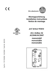
USER MANUAL CR2041 IFM

Prise M12, 5 pôles, codage A (Con. 1...8, CAN OUT)
1:LEDIN07
2:LEDIN15
3:LEDIN05
4:LEDIN13
5:LEDIN03
6:LEDIN11
7:LEDIN01
8:LEDIN09
9:LEDIN08
10:LEDIN00
11:LEDIN10
12:LEDIN02
13:LEDIN12
14:LEDIN04
15:LEDIN14
16:LEDIN06
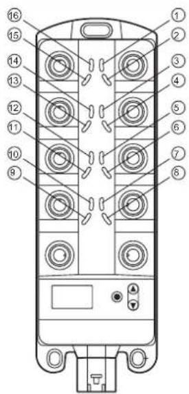
Abréviations A
Analogue
BH TOR niveau haut
BL TOR nivea bas
LED E/S 16 x LED orange
LED Power (PWR) LED verte
LED Mode (M) LED verte
LED d'application (A...D)
LED Lock (symbole de cadenas)
LED de diagnostic (DIA)
Affichage
A, BD, CC, DB, DC, DD,

Prise M12, 5 pôles, codage A (Con. 1...8, CAN OUT)

Prise M12, 5 pôles, codage A (Con. 1...8, CAN OUT)
The following error codes according to DSP-401 or DSP-301 are supported:
| EMCY code | Error reg | Additive | Onal code Description |
| 0x6100 0x11 | 0x00 "Internal Software | Overflow of an Rx queue e.g. frequency of the RxP-DOs is too high. Reset only externally via entry in the indey 0x1003 SubIdx 00." | |
| 0x6101 0x11 | 0x00 "Internal Software | Overflow of an Tx queue e.g. device does not communicate with the bus. Reset only externally via entry in the indey 0x1003 SubIdx 00." | |
| 0x8000 0x11 | 0x00 "Monitoring Sync Error | For communication cycle no sync object is received. Only in Operational. Reset with the next sync OBJ or PREOP" | |
| 0x8100 0x11 | 0x00 Communication Err | ||
| 0x8131 0x11 | 0x00 "Monitoring Heart Beat Error | No guard object is received. Reset with the next Heart beat or PREOP" | |
| 0x63xx 0x01 | 0x00 "Invalid parameter of an input or output. ""xx"" means number of the IO-channel (00 ... 15)" | ||
| 0x5000 0x01 | 0x00 Memory Error | ||
| 0x3308 0x05 | 0x00 VBB2 error (only CR2041, CR2042) | ||
| 0x90xx 0x01 | 0x00 "Frequency input, Frequency too low" | ||
| 0x21xx 0x03 | 0x00 "Inputs, Openline" | ""xx"" means number of the IO-channel (00 ... 15)" | |
| 0x21xx 0x03 | 0x00 "Inputs, Short circuit" | ""xx"" means number of the IO-channel (00 ... 15)" | |
| 0x21xx 0x03 | 0x00 "Inputs, Overcurrent" | ""xx"" means number of the IO-channel (00 ... 15) + 16; CR2042 (00 ... 07) + 8" | |
| 0x23xx 0x03 | 0x00 "outputs, Openline" | ""xx"" means number of the IO-channel CR2041 (00 ... 15); CR2042 (00 ... 07)" | |
| 0x23xx 0x03 | 0x00 "outputs, Short circuit" | ""xx"" means number of the IO-channel CR2041 (00 ... 15) + 16; CR2042 (00 ... 07) + 8" | |
| 0x23xx 0x03 | 0x00 "outputs, Overload" | ""xx"" means number of the IO-channel CR2041 (00 ... 15) + 32; CR2042 (00 ... 07) + 16" | |
CANopen does not provide for two identical EMCY objects to be sent consecutively.
12.2 Object directory CR204x
Obligatory objects (index 0x1000...0x1FFF):
| Index S-index Design Data type Default Details | |||||||||
| 0x1000 Device type ro UDINT 0x000F0191 Device type | |||||||||
| 0x1001 Error register ro USINT 0 Error register bit coded to profile | 301 Permissible values: 0b0000 0000 = no error 0b0000 0001 = generic error 0b0001 0000 = communication error 0b1000 0000 = manufacturer specific | ||||||||
| 0x1018 0x00 Device identification Number of entries | ro USINT 0x04 | Device | identification | ||||||
| 0x01 | Vendor-ID | ro | UDINT | 0x0069666D | Vendor ID oft he device according to CiA specification | ||||
| 0x02 | Product code ro STRING 0 Product code of the device | ||||||||
| 0x03 | Revision number | ro UDINT 0 Revision number of the device | |||||||
| 0x04 | Serial number | ro UDINT 0 Serial number of the device | |||||||
| 0x1003 0x00 Predefined error field Number of entries | rw | UDINT 0 An error list with 4 entries is supported | |||||||
| 0x01 | Error history | ro UDINT 0 Error occurred, coded according to EMCY list The last error is indicated in the sub-index 1 | |||||||
| 0x02 | Error history | ro UDINT 0 Error occurred, coded according to EMCY list | |||||||
| 0x03 | Error history | ro UDINT 0 Error occurred, coded according to EMCY list | |||||||
| 0x04 | Error history | ro UDINT 0 Error occurred, coded according to EMCY list | |||||||
| 0x05 | Error history | ro UDINT 0 Error occurred, coded according to EMCY list | |||||||
| Index S-index Design Data type | Default Details | ||||||||
| 0x1005 | COB-ID | synch message | rw U | DINT 0x000 | 0080 Identifier of the synch messageBit 30 = 0 → device generates no synch messageBit 30 = 1 → device generates a synch messageBit 29 = 0 → 11 bit IDBit 29 = 1 → ID = 0x80 + node ID | ||||
| 0x1006 | Communication cycle period | rw U | DINT 0 Max. time between 2 synch objects in [μs]Control resolution = 1 ms | ||||||
| 0x1008 | Manufacturer device name | ro STRING CR204x Device designation (CR2040 or CR2041 or CR2042) | |||||||
| 0x1009 | Manufacturer hardware version | ro STRING V00.00.00 Hardware version | |||||||
| 0x100A | Manufacturer software version | ro STRING V00.00.00 Software version | |||||||
| 0x1010 | 0x00 | Store parametersLargest sub-index supported | ro USINT 0x01 | Number of "save options" | |||||
| 0x01 | Save all parameters | rw U | DINT 2 Automatic saving of all parameters changed0 = AutoSave OFF2 = AutoSave ON | ||||||
| 0x1011 | 0x00 | Restore default parametersLargest sub-index supported | ro USINT 0x01 | Number of "restore options" | |||||
| 0x01 | Restore all default parameters | rw U | DINT 0x01 | If the String "load" is entered here, the default parameters set at the factory are restored and become valid after the next reset. | |||||
| 0x1014 | COBIidEmergency | rw | UDINT | 0x80 + node ID | Bit 31 = 0 → EMCY is validBit 31 = 1 → EMCY is not validBit 29 = 0 → 11-bit IDBit 29 = 1 → ID = 0x80 + node IDCAN identifier can be changed by the user. | ||||
| Index S-index Design Data type Default Details | |||||||||
| 0x1016 | 0x00 | Consumer heartbeat times | ro USINT 0x01 Heartbeat monitoring | time for the nodeNumber of devices monitored = 1 | |||||
| Numbers consumer heartbeat time | |||||||||
| 0x01 | Consumer heartbeat time | rw USINT 0 Heartbeat monitoring | time for the nodeFormat: 0x0nntttttt tt=monitoring time [ms] nn = node numberif nn=0 or tttt=0 → no monitoring | ||||||
| 0x1017 | Producer | heartbeat time | rw USINT 0 Time | interval [ms] during | which the device generates a producer heartbeat | ||||
12.2.1 Device-specific CR2040
Transmit PDO communication parameters (index 0x1800...0x18FF):
| Index Sidx Designation Data type Default Details | |||||
| 0x1800 0x00 TransmitPDO Com-municationParameterNumber ofentries | ro USINT 0x05 Configuration transmit PDO 1number of entries = 5 | ||||
| 0x01 COBID usedby PDO | rw USINT 0x180 +Node ID | CAN ID of the transmit PDO 1Bit 31 = 0 → PDO is validBit 31 = 1 → PDO is not valid | |||
| 0x02 transmissiontype | rw USINT 0xFF 0x00 = synch acyclic0x01...0xF0 = synch cyclic; valuesare only transmitted after „n" synchobjectsn = 1...240 = 0x01...0xF00xFC/0xCD not implemented0xFE = asynch man. spec. event;values are immediately transferred0xFF = asynch device profile event;values are immediately transferred | ||||
| 0x03 inhibit time rw UINT | 0 | delay time | in the transmissiontype "asynch" before the PDO istransmitted again at the earliest.(0...65535 · 100 μs) | ||
| 0x04 reserved rw USINT 0 | reserve | ||||
| 0x05 event time | rw | UINT | 0 | max. transfer break in the transmissi-on type „asynch" (0...65535 ms)When this time has elapsed, the PDOis transferred even if the appl. eventhas not accured. | |
| 0x1801 0x00 TransmitPDO Com-municationParameterNumber ofentries | ro USINT 0x05 Configuration transmit PDO 2number of entries = 5 | ||||
| 0x01 COBID usedby PDO | rw USINT 0x280 +Node ID | CAN ID of the transmit PDO 2Bit 31 = 0 → PDO is validBit 31 = 1 → PDO is not valid | |||
| 0x02 transmissiontype | rw USINT 0x01 0x00 = synch acyclic0x01...0xF0 = synch cyclic; valuesare only transmitted after „n" synchobjectsn = 1...240 = 0x01...0xF00xFC/0xCD not implemented0xFE = asynch man. spec. event;values are immediately transferred0xFF = asynch device profile event;values are immediately transferred | ||||
| 0x03 inhibit time rw UINT 0 delay time inthe transmission | type "asynch" before the PDO istransmitted again at the earliest.(0...65535 · 100 μs) | ||||
| 0x04 reserved rw USINT 0 reserve | |||||
| 0x05 event time rw UINT 0 max. transfer break in thetransmissi-on type „asynch" (0...65535 ms)When this time has elapsed, the PDOis transferred even if the appl. eventhas not accured. | |||||
| 0x1802 0x00 TransmitPDO Com-municationParameterNumber ofentries | ro USINT 0x05 Configuration transmit PDO 3number of entries = 5 | ||||
| 0x01 COBID usedby PDO | rw USINT 0x380 +Node ID | CAN ID of the transmit PDO 3Bit 31 = 0 → PDO is validBit 31 = 1 → PDO is not valid | |||
| 0x02 transmissiontype | rw USINT 0x01 0x00 = synch acyclic0x01...0xF0 = synch cyclic; valuesare only transmitted after „n" synchobjectsn = 1...240 = 0x01...0xF00xFC/0xFD not implemented0xFE = asynch man. spec. event;values are immediately transferred0xFF = asynch device profile event;values are immediately transferred | ||||
| 0x03 inhibit time rw UART 0 delay time inthe transmission | type "asynch" before the PDO istransmitted again at the earliest.(0...65535 · 100 μs) | ||||
| 0x04 reserved rw USINT 0 reserve | |||||
| 0x05 event time rw UART 0 max. transfer break in thetransmissi-on type „asynch" (0...65535 ms)When this time has elapsed, the PDOis transferred even if the appl. eventhas not accured. | |||||
| 0x1803 0x00 TransmitPDO Com-municationParameterNumber ofentries | ro USINT 0x05 Configuration transmit PDO 4number of entries = 5 | ||||
| 0x01 COBID usedby PDO | rw USINT 0x480 +Node ID | CAN ID of the transmit PDO 4Bit 31 = 0 → PDO is validBit 31 = 1 → PDO is not valid | |||
| 0x02 transmissiontype | rw USINT 0x01 0x00 = synch acyclic0x01...0xF0 = synch cyclic; valuesare only transmitted after „n" synchobjectsn = 1...240 = 0x01...0xF00xFC/0xFD not implemented0xFE = asynch man. spec. event;values are immediately transferred0xFF = asynch device profile event;values are immediately transferred | ||||
| 0x03 inhibit time rw UART 0 delay time inthe transmission | type "asynch" before the PDO istransmitted again at the earliest.(0...65535 · 100 μs) | ||||
| 0x04 reserved rw USINT 0 reserve | |||||
| 0x05 event time rw UART 0 max. transfer break in thetransmissi-on type „asynch" (0...65535 ms)When this time has elapsed, the PDOis transferred even if the appl. eventhas not accured. | |||||
| 0x1804 0x00 TransmitPDO Com-municationParameterNumber ofentries | ro USINT 0x05 Configuration transmit PDO 5number of entries = 5 | ||||
| 0x01 COBID usedby PDO | rw USINT 0x181 +Node ID | CAN ID of the transmit PDO 5Bit 31 = 0 → PDO is validBit 31 = 1 → PDO is not valid | |||
| 0x02 transmissiontype | rw USINT 0x01 0x00 = synch acyclic0x01...0xF0 = synch cyclic; valuesare only transmitted after „n" synchobjectsn = 1...240 = 0x01...0xF00xFC/0xCD not implemented0xFE = asynch man. spec. event;values are immediately transferred0xFF = asynch device profile event;values are immediately transferred | ||||
| 0x03 inhibit time rw UART 0 delay time inthe transmission | type "asynch" before the PDO istransmitted again at the earliest.(0...65535 · 100 μs) | ||||
| 0x04 reserved rw USINT 0 reserve | |||||
| 0x05 event time rw UART 0 max. transfer break in thetransmissi-on type „asynch" (0...65535 ms)When this time has elapsed, the PDOis transferred even if the appl. eventhas not accured. | |||||
| 0x1805 0x00 TransmitPDO Com-municationParameterNumber ofentries | ro USINT 0x05 Configuration transmit PDO 6number of entries = 5 | ||||
| 0x01 COBID usedby PDO | rw USINT 0x281 +Node ID | CAN ID of the transmit PDO 6Bit 31 = 0 → PDO is validBit 31 = 1 → PDO is not valid | |||
| 0x02 transmissiontype | rw USINT 0x01 0x00 = synch acyclic0x01...0xF0 = synch cyclic; valuesare only transmitted after „n" synchobjectsn = 1...240 = 0x01...0xF00xFC/0xCD not implemented0xFE = asynch man. spec. event;values are immediately transferred0xFF = asynch device profile event;values are immediately transferred | ||||
| 0x03 inhibit time rw UART 0 delay time inthe transmission | type "asynch" before the PDO istransmitted again at the earliest.(0...65535 · 100 μs) | ||||
| 0x04 reserved rw USINT 0 reserve | |||||
| 0x05 event time rw UART 0 max. transfer break in thetransmissi-on type „asynch" (0...65535 ms)When this time has elapsed, the PDOis transferred even if the appl. eventhas not accured. | |||||
Index S-idx Designation Data type Default Details
| 0x1806 0x00 Transmit | ro USINT 0x05 Configuration transmit PDO 7 | |||||
| PDO Com-munication | number of entries = 5 | |||||
| Parameter | ||||||
| Number of entries | ||||||
| 0x01 COBID used by PDO | rw UDINT 0x381 + Node ID | CAN ID of the transmit PDO 7 Bit 31 = 0 → PDO is valid Bit 31 = 1 → PDO is not valid | ||||
| 0x02 transmission type | rw USINT 0x01 0x00 = synch acyclic | |||||
| 0x01...0xF0 = synch cyclic; values are only transmitted after „n" synch objects n = 1...240 = 0x01...0xF0 0xFC/0xCD not implemented 0xFE = asynch man. spec. event; values are immediately transferred 0xFF = asynch device profile event; values are immediately transferred | ||||||
| 0x03 inhibit time rw UINT 0 delay time in the transmission | type "asynch" before the PDO is transmitted again at the earliest. (0...65535 · 100 μs) | |||||
| 0x04 reserved rw USINT 0 reserve | ||||||
| 0x05 event time | rw UINT 0 max. transfer break in the transmis-si-on type „asynch" (0...65535 ms) When this time has elapsed, the PDO is transferred even if the appl. event has not accured. | |||||
| Index Sidx Designation Data type Default Details | ||||||
| 0x1807 0x00 TransmitPDO Com-municationParameterNumber ofentries | ro USINT 0x05 Configuration transmit PDO 8number of entries = 5 | |||||
| 0x01 COBID usedby PDO | rw USINT 0x481 +Node ID | CAN ID of the transmit PDO 8Bit 31 = 0 → PDO is validBit 31 = 1 → PDO is not valid | ||||
| 0x02 transmissiontype | rw USINT 0x01 0x00 = synch acyclic0x01...0xF0 = synch cyclic; valuesare only transmitted after „n" synchobjectsn = 1...240 = 0x01...0xF00xFC/0xCD not implemented0xFE = asynch man. spec. event;values are immediately transferred0xFF = asynch device profile event;values are immediately transferred | |||||
| 0x03 inhibit time rw UART 0 delay time inthe transmission | type "asynch" before the PDO istransmitted again at the earliest.(0...65535 · 100 μs) | |||||
| 0x04 reserved rw USINT 0 reserve | ||||||
| 0x05 event time rw UART 0 max. transfer break in thetransmissi-on type „asynch" (0...65535 ms)When this time has elapsed, the PDOis transferred even if the appl. eventhas not accured. | ||||||
| 0x1808 0x00 TransmitPDO Com-municationParameterNumber ofentries | ro USINT 0x05 Configuration transmit PDO 9number of entries = 5 | |||||
| 0x01 COBID usedby PDO | rw USINT 0x182 +Node ID | CAN ID of the transmit PDO 9Bit 31 = 0 → PDO is validBit 31 = 1 → PDO is not valid | ||||
| 0x02 transmissiontype | rw USINT 0x01 0x00 = synch acyclic0x01...0xF0 = synch cyclic; valuesare only transmitted after „n" synchobjectsn = 1...240 = 0x01...0xF00xFC/0xCD not implemented0xFE = asynch man. spec. event;values are immediately transferred0xFF = asynch device profile event;values are immediately transferred | |||||
| 0x03 inhibit time rw UART 0 delay time inthe transmission | type "asynch" before the PDO istransmitted again at the earliest.(0...65535 · 100 μs) | |||||
| 0x04 reserved rw USINT 0 reserve | ||||||
| 0x05 event time rw UART 0 max. transfer break in thetransmissi-on type „asynch" (0...65535 ms)When this time has elapsed, the PDOis transferred even if the appl. eventhas not accured. | ||||||
| 0x1809 0x00 TransmitPDO Com-municationParameterNumber ofentries | ro USINT 0x05 Configuration transmit PDO 10number of entries = 5 | |||||
| 0x01 COBID usedby PDO | rw USINT 0x282 +Node ID | CAN ID of the transmit PDO 10Bit 31 = 0 → PDO is validBit 31 = 1 → PDO is not valid | ||||
| 0x02 transmissiontype | rw USINT 0x01 0x00 = synch acyclic0x01...0xF0 = synch cyclic; valuesare only transmitted after „n" synchobjectsn = 1...240 = 0x01...0xF00xFC/0xCD not implemented0xFE = asynch man. spec. event;values are immediately transferred0xFF = asynch device profile event;values are immediately transferred | |||||
| 0x03 inhibit time rw UART 0 delay time inthe transmission | type "asynch" before the PDO istransmitted again at the earliest.(0...65535 · 100 μs) | |||||
| 0x04 reserved rw USINT 0 reserve | ||||||
| 0x05 event time rw UART 0 max. transfer break in thetransmissi-on type „asynch" (0...65535 ms)When this time has elapsed, the PDOis transferred even if the appl. eventhas not accured. | ||||||
Transmit PDO mapping (index 0x1A00...0x1AFF):
| Index S-index Design Data type Default Details | ||||||
| 0x1A00 | 0x00 TransmitPDO map-pingNumber of mapped objects in PDO | rw USINT 0x07 mapping transmit | PDO 1number of integrated applicationobjects = 7 | |||
| 0x01 PDO map-ping | rw USINT 0x60000108 Index 0x6000, SubIndex 0x01binary inputs 00...07: actual values(bit coded) | |||||
| 0x02 PDO map-ping | rw USINT 0x60000208 Index 0x6000, SubIndex 0x02binary inputs 08...15: actual values(bit coded) | |||||
| 0x03 PDO map-ping | rw USINT 0x20200108 Index 0x2020, SubIndex 0x01binary inputs 00...07: flag "shortcircuit" (bit coded) | |||||
| 0x04 PDO map-ping | rw USINT 0x20200208 Index 0x2020, SubIndex 0x02binary inputs 08...15: flag "shortcircuit" (bit coded) | |||||
| 0x05 PDO map-ping | rw USINT 0x20210108 Index 0x2021, SubIndex 0x01outputs 00...07: flag " wire break " (bit coded) | |||||
| 0x06 PDO map-ping | rw USINT 0x20210208 Index 0x2021, SubIndex 0x02outputs 08...15: flag " wire break " (bit coded) | |||||
| 0x07 PDO map-ping | rw USINT 0x20250108 Index 0x2025, SubIndex 0x01inputs 00...03: flag " overload " (bit coded) | |||||
| Index Sidx Design Data type | ||||||
| 0x1A01 | 0x00 TransmitPDO map-pingNumber of mapped objects in PDO | rw USINT 0x04 mapping transmit | PDO 2 (analogue inputs)number of integrated application objects = 4 | |||
| 0x01 PDO map-ping | rw USINT 0x64040110 Index 0x6404, SubIndex 0x01 analogue input 00: actual value (depending on the configuration 0x2000) | |||||
| 0x02 PDO map-ping | rw USINT 0x64040210 Index 0x6404, SubIndex 0x02 analogue input 01: actual value (depending on the configuration 0x2000)) | |||||
| 0x03 PDO map-ping | rw USINT 0x64040310 Index 0x6404, SubIndex 0x03 analogue input 02: actual value (depending on the configuration 0x2000) | |||||
| 0x04 PDO map-ping | rw USINT 0x64040410 Index 0x6404, SubIndex 0x04 analogue input 03: actual value (depending on the configuration 0x2000) | |||||
| 0x1A02 | 0x00 TransmitPDO map-pingNumber of mapped objects in PDO | rw USINT 0x04 mapping transmit | PDO 3 (analogue inputs)number of integrated application objects = 4 | |||
| 0x01 PDO map-ping | rw USINT 0x64040510 Index 0x6404, SubIndex 0x05 analogue input 04: actual value (depending on the configuration 0x2000) | |||||
| 0x02 PDO map-ping | rw USINT 0x64040610 Index 0x6404, SubIndex 0x06 analogue input 05: actual value (depending on the configuration 0x2000)) | |||||
| 0x03 PDO map-ping | rw USINT 0x64040710 Index 0x6404, SubIndex 0x07 analogue input 06: actual value (depending on the configuration 0x2000) | |||||
| 0x04 PDO map-ping | rw USINT 0x64040810 Index 0x6404, SubIndex 0x08 analogue input 07: actual value (depending on the configuration 0x2000) | |||||
| Index S-idx Design Data type | Default Details | |||||
| 0x1A03 | 0x00 TransmitPDO mappingNumber of mapped objects in PDO | rw USINT 0x04 mapping transmit | PDO 4number of integrated applicationobjects = 4 | |||
| 0x01 PDO mapping | rw USINT 0x20300110 Index 0x2030, SubIndex 0x01input 08: actual resistor value | |||||
| 0x02 PDO mapping | rw USINT 0x20300210 Index 0x2030, SubIndex 0x02input 10: actual resistor value | |||||
| 0x03 PDO mapping | rw USINT 0x20300310 Index 0x2030, SubIndex 0x03input 12: actual resistor value | |||||
| 0x04 PDO mapping | rw USINT 0x20300410 Index 0x2030, SubIndex 0x04input 14: actual resistor value | |||||
| 0x1A04 | 0x00 TransmitPDO mappingNumber of mapped objects in PDO | rw USINT 0x02 mapping transmit | PDO 5 (periodetime IN09, IN11)number of integrated applicationobjects = 2 | |||
| 0x01 PDO mapping | rw USINT 0x20120120 Index 0x2012, SubIndex 0x01frequency input IN09: periode time ofthe signal | |||||
| 0x02 PDO mapping | rw USINT 0x20120220 Index 0x2012, SubIndex 0x02frequency input IN11: periode time ofthe signal | |||||
| 0x1A05 | 0x00 TransmitPDO mappingNumber of mapped objects in PDO | rw USINT 0x02 mapping transmit | PDO 6 (periodetime IN13, IN15)number of integrated applicationobjects = 2 | |||
| 0x01 PDO mapping | rw USINT 0x20120320 Index 0x2012, SubIndex 0x03frequency input IN13: periode time ofthe signal | |||||
| 0x02 PDO mapping | rw USINT 0x20120420 Index 0x2012, SubIndex 0x04frequency input IN15: periode time ofthe signal | |||||
| Index S-index Design Data type Default Details | ||||||
| 0x1A06 | 0x00 TransmitPDO mappingNumber of mapped objects in PDO | rw USINT 0x04 mapping transmit | PDO 7 (duty cycle of the signal on the frequency input IN09, IN11, IN13, IN15) number of integrated application objects = 4 | |||
| 0x01 DO mapping | rw USINT 0x2014 0110 Index 0x2014, SubIndex 0x01 frequency input IN09: duty cycle of the signal in %o | |||||
| 0x02 DO mapping | rw USINT 0x2014 0210 Index 0x2014, SubIndex 0x02 frequency input IN11: duty cycle of the signal in %o | |||||
| 0x03 DO mapping | rw USINT 0x2014 0310 Index 0x2014, SubIndex 0x03 frequency input IN13: duty cycle of the signal in %o | |||||
| 0x04 DO mapping | rw USINT 0x2014 0410 Index 0x2014, SubIndex 0x04 frequency input IN15: duty cycle of the signal in %o | |||||
| 0x1A07 | 0x00 TransmitPDO mappingNumber of mapped objects in PDO | rw USINT 0x02 mapping transmit | PDO 8 (frequency on IN09, IN11) number of integrated application objects = 2 | |||
| 0x01 DO mapping | rw USINT 0x2015 0120 Index 0x2015, SubIndex 0x01 frequency input IN09: frequency value of the signal in Hz | |||||
| 0x02 DO mapping | rw USINT 0x2015 0220 Index 0x2015, SubIndex 0x02 frequency input IN11: frequency value of the signal in Hz | |||||
| 0x1A08 | 0x00 TransmitPDO mappingNumber of mapped objects in PDO | rw USINT 0x02 mapping transmit | PDO 9 (frequency on IN13, IN15) number of integrated application objects = 2 | |||
| 0x01 DO mapping | rw USINT 0x2015 0320 Index 0x2015, SubIndex 0x03 frequency input IN13: frequency value of the signal in Hz | |||||
| 0x02 DO mapping | rw USINT 0x2015 0420 Index 0x2015, SubIndex 0x04 frequency input IN15: frequency value of the signal in Hz | |||||
| 0x1A09 0x00 TransmitPDO map-pingNumber ofmappedobjects inPDO | rw USINT 0x02 mapping transmit | PDO 10 (systemflag)number of integrated applicationobjects = 2 | ||||
| 0x01 PDO map-ping | rw U DINT 0x204 00110 Index 0x2040, SubIndex 0x01supply voltage of the system VBSS | |||||
| 0x02 PDO map-ping | rw U DINT 0x205 00010 Index 0x2050, SubIndex 0x00system temperature in °C | |||||
Manufacturer-specific objekts (index 0x2000...0x6FFF):
| Index S-index Design Data type Default Details | ||||||
| 0x2000 0x00 IO configuration Largest sub-index supported | ro USINT 16 Configuration inputs | outputs largest supported Sub-index = 32 | ||||
| 0x01 Configuration IN00 | rw USINT 10 0 = 0x00 | 3 = 0x036 = 0x067 = 0x079 = 0x0910 = 0x0A11 = 0x0B12 = 0x0C | off Input IN000...10 000 mV ratiometric 0...1000 %0...20 000 μA0...32 000 mV binary plus switched binary plus switched with diagnosis binary minus switched | |||
| 0x02 Configuration IN01 | rw USINT 10 0 = 0x00 | 3 = 0x036 = 0x067 = 0x079 = 0x0910 = 0x0A11 = 0x0B12 = 0x0C | off Input IN010...10 000 mV ratiometric 0...1000 %0...20 000 μA0...32 000 mV binary plus switched binary plus switched with diagnosis binary minus switched | |||
| 0x03 Configuration IN02 | rw USINT 10 0 = 0x00 | 3 = 0x036 = 0x067 = 0x079 = 0x0910 = 0x0A11 = 0x0B12 = 0x0C | off Input IN020...10 000 mV ratiometric 0...1000 %0...20 000 μA0...32 000 mV binary plus switched binary plus switched with diagnosis binary minus switched | |||
| Index Sidx Designation Data type Default Details | ||||||
| 0x2000 | 0x04 ConfigurationIN03 | rw USINT 10 0 = | 0x00 | 3 = 0x036 = 0x067 = 0x079 = 0x0910 = 0xA11 = 0xB12 = 0xC | off Input IN030...10 000 mV ratiometric 0...1000 %0...20 000 μA0...32 000 mV binary plus switched binary plus switched with diagnosis binary minus switched | |
| 0x05 ConfigurationIN04 | rw USINT 10 0 = | 0x00 | 3 = 0x036 = 0x067 = 0x079 = 0x0910 = 0xA11 = 0xB12 = 0xC | off Input IN040...10 000 mV ratiometric 0...1000 %0...20 000 μA0...32 000 mV binary plus switched binary plus switched with diagnosis binary minus switched | ||
| 0x06 ConfigurationIN05 | rw USINT 10 0 = | 0x00 | 3 = 0x036 = 0x067 = 0x079 = 0x0910 = 0xA11 = 0xB12 = 0xC | off Input IN050...10 000 mV ratiometric 0...1000 %0...20 000 μA0...32 000 mV binary plus switched binary plus switched with diagnosis binary minus switched | ||
| 0x07 ConfigurationIN06 | rw USINT 10 0 = | 0x00 | 3 = 0x036 = 0x067 = 0x079 = 0x0910 = 0xA11 = 0xB12 = 0xC | off Input IN060...10 000 mV ratiometric 0...1000 %0...20 000 μA0...32 000 mV binary plus switched binary plus switched with diagnosis binary minus switched | ||
| 0x08 ConfigurationIN07 | rw USINT 10 0 = | 0x00 | 3 = 0x036 = 0x067 = 0x079 = 0x0910 = 0xA11 = 0xB12 = 0xC | off Input IN070...10 000 mV ratiometric 0...1000 %0...20 000 μA0...32 000 mV binary plus switched binary plus switched with diagnosis binary minus switched | ||
| 0x09 ConfigurationIN08 | rw USINT 10 0 = | 0x00 | 10 = 0xA11 = 0xB18 = 0x12 | off Input IN08binary plus switched binary plus switched with diagnosis 16...30 000 Ohm | ||
| Index S-index Design Data type Default Details | ||||||
| 0x2000 | 0x0A Configuration IN09 | rw USINT 01 0 = 0x00 | 01 = 0x0114 = 0xE20 = 0x14 | off Input IN09 binary plus switched frequency0...30 000 Hz period duration | ||
| 0x0B Configuration IN10 | rw USINT 10 0 = 0x00 | 10 = 0xA11 = 0xB18 = 0x12 | off Input IN10 binary plus switched binary plus switched with diagnosis16...30 000 Ohm | |||
| 0x0C Configuration IN11 | rw USINT 01 0 = 0x00 | 01 = 0x0114 = 0xE20 = 0x14 | off Input IN11 binary plus switched frequency0...30 000 Hz period duration | |||
| 0x0D Configuration IN12 | rw USINT 10 0 = 0x00 | 10 = 0xA11 = 0xB18 = 0x12 | off Input IN12 binary plus switched binary plus switched with diagnosis16...30 000 Ohm | |||
| 0x0E Configuration IN13 | rw USINT 01 0 = 0x00 | 01 = 0x0114 = 0xE20 = 0x14 | off Input IN12 binary plus switched frequency0...30 000 Hz period duration | |||
| 0x0F Configuration IN14 | rw USINT 10 0 = 0x00 | 10 = 0xA11 = 0xB18 = 0x12 | off Input IN14 binary plus switched binary plus switched with diagnosis16...30 000 Ohm | |||
| 0x10 Configuration IN15 | rw USINT 01 0 = 0x00 | 01 = 0x0114 = 0xE20 = 0x14 | off Input IN15 binary plus switched frequency0...30 000 Hz period duration | |||
| 0x2012 | 0x00 Period input ro USINT 4 | Largest subindex supported | ||||
| 0x01 Period durati-on IN09 | ro | UDINT | 0 | IN09 period duration [μs] | ||
| 0x02 Period durati-on IN11 | ro | UDINT | 0 | IN11 period duration [μs] | ||
| 0x03 Period durati-on IN13 | ro | UDINT | 0 | IN13 period duration [μs] | ||
| 0x04 Period durati-on IN15 | ro | UDINT | 0 | IN15 period duration [μs] | ||
| Index Sidx Designation Data type | Default Details | ||||||
| 0x2013 0x00 Period input number of periods for average | ro USINT 4 Largest sub-index supported | ||||||
| 0x01 Numb der input number of periods IN09 | rw USINT 4 1...255 IN09 number of | periods | |||||
| 0x02 Numb der input period s IN11 | rw USINT 4 1...255 IN11 number of | periods | |||||
| 0x03 Numb der input period s IN13 | rw USINT 4 1...255 IN13 number of | periods | |||||
| 0x04 Numb der input period s IN15 | rw USINT 4 1...255 IN15 number of | periods | |||||
| 0x2014 0x00 Period input - ratio value | ro USINT 4 Largest sub-index supported | ||||||
| 0x01 Period ratio value IN09 | ro UINT 0 0...1 000 IN09 marc-to-space | ratio [%] | |||||
| 0x02 Period ratio value IN11 | ro UINT 0 0...1 000 IN11 marc-to-space | ratio [%] | |||||
| 0x03 Period ratio value IN13 | ro UINT 0 0...1 000 IN13 marc-to-space | ratio [%] | |||||
| 0x04 Period ratio value IN15 | ro UINT 0 0...1 000 IN15 marc-to-space | ratio [%] | |||||
| 0x2015 0x00 Frequency input | ro USINT 4 Largest sub-index supported | ||||||
| 0x01 Frequency IN09 | ro REAL 1 0...30 000 IN09 frequency [Hz] | ||||||
| 0x02 Frequency IN11 | ro REAL 1 0...30 000 IN11 frequency [Hz] | ||||||
| 0x03 Frequency IN13 | ro REAL 1 0...30 000 IN13 frequency [Hz] | ||||||
| 0x04 Frequency IN15 | ro REAL 1 0...30 000 IN15 frequency [Hz] | ||||||
| 0x2016 0x00 Timebase ro USINT 4 Largest sub-index supported | |||||||
| 0x01 Timebase IN09 | rw UINT 50 | 0...2 000 IN09 timebase [ms] | |||||
| 0x02 Timebase IN11 | rw UINT 50 | 0...2 000 IN11 timebase [ms] | |||||
| 0x03 Timebase IN13 | rw UINT 50 | 0...2 000 IN13 timebase [ms] | |||||
| 0x04 Timebase IN15 | rw UINT 50 | 0...2 000 IN15 timebase [ms] | |||||
| Index S-index Design Data type Default Details | ||||||
| 0x2020 | 0x00 Input - short to supply voltage | ro USINT 2 Largest sub-index supported | ||||
| 0x01 Short to supply voltage IN00...IN07 | ro USINT 0 0 = normal | 1 = short circuit | channels (bit coded)0b---- ---X = IN000b---- --X- = IN010b---- -X-- = IN020b---- X--- = IN030b---- X---- = IN040b---- -X- = IN050b-X---- = IN060bX---- = IN07 | |||
| 0x02 Short to supply voltage IN08, IN10, IN12, IN14 | ro USINT 0 0 = normal | 1 = short circuit | channels (bit coded)0b---- ---X = IN080b---- --X- = IN100b---- -X-- = IN120b---- X---- = IN14 | |||
| 0x2021 | 0x00 Input - wire break | ro USINT 2 Largest sub-index supported | ||||
| 0x01 Wire break IN00...IN07 | ro USINT 0 0 = normal | 1 = wire break | channels (bit coded)0b---- ---X = IN000b---- --X- = IN010b---- -X-- = IN020b---- X--- = IN030b---- X---- = IN040b---- -X- = IN050b-X---- = IN060bX---- = IN07 | |||
| 0x02 Wire break IN08, IN10, IN12, IN14 | ro USINT 0 0 = normal | 1 = wire break | channels (bit coded)0b---- ---X = IN080b---- --X- = IN100b---- -X-- = IN120b---- X---- = IN14 | |||
| 0x2025 | 0x00 Input analog - overcurrent | ro USINT 1 Largest sub-index supported | ||||
| 0x01 Overcurrent IN00...IN07 | ro USINT 0 0 = normal | 1 = overcurrent | channels (bit coded)0b---- ---X = IN000b---- --X- = IN010b---- -X-- = IN020b---- X--- = IN030b---- X---- = IN040b-X---- = IN050b-X---- = IN060bX---- = IN07 | |||
| Index S-index Design Data type | |||||||
| 0x2030 | 0x00 Input resistor ro USIN4 Largest sub-index supported | ||||||
| 0x01 ResistanceIN08 | ro UINT 0 0...30 | 000 IN08 resistance | [Ohms] | ||||
| 0x02 ResistanceIN10 | ro UINT 0 0...30 | 000 IN10 resistance | [Ohms] | ||||
| 0x03 ResistanceIN12 | ro UINT 0 0...30 | 000 IN12 resistance | [Ohms] | ||||
| 0x04 ResistanceIN14 | ro UINT 0 0...30 | 000 IN14 resistance | [Ohms] | ||||
| 0x2040 | 0x00 System supp-ly voltageVBBS | ro USINT 1 Largest sub-index supported | |||||
| 0x01 VBBS ro USINT 0 VBB$ voltage [mV] | |||||||
| 0x2050 | Device temperature | ro UINT 0 temperature [°C] | |||||
| 0x20F0 | Node ID | rw | USINT | 125 | 1...125 | node ID[!] value(0x20F0) !=value(20F1) | |
| 0x20F1 | Node ID | rw | USINT | 125 | 1...125 | node ID[!] value(0x20F0) !=value(20F1) | |
| 0x20F2 | Baud rate | rw USINT 3 baud rate | [!] value(0x20F2) != value(20F3) | ||||
| 0 | 1000 kBits/s | ||||||
| 1 | 800 kBits/s | ||||||
| 2 | 500 kBits/s | ||||||
| 3 | 250 kBits/s | ||||||
| 4 | 125 kBits/s | ||||||
| 5 | 100 kBits/s | ||||||
| 6 | 50 kBits/s | ||||||
| 7 | 20 kBits/s | ||||||
| 0x20F3 | Baud rate | rw USINT 3 baud rate | [!] value(0x20F2) != value(20F3) | ||||
| 0x20F4 | Autostart | rw UART 0 not used | |||||
| 0x20F5 | Lock edit | mode | rw USINT 0 0 =edit mode unlocked | 1 = edit mode locked | |||
| 0x20F6 | CAN inter-face | rw USINT 1 1...2 | CAN interface | [!] value(0x20F6) !=value(20F7) | |||
| 0x20F7 | CAN inter-face | rw USINT 1 1...2 | CAN interface | [!] value(0x20F6) !=value(20F7) | |||
| Index S-index Designation Data type | pe Default Details | ||||
| 0x6000 | 0x00 Binary inputLargestsub-indexsupported | ro USINT 0x02 Binary inputs | Largest supported sub-index = 2 | ||
| 0x01 Binary inputsIN00 - IN07 | ro USINT 0 BinaIy inputs IN00... | N070b---- ---X = IN000b---- -X- = IN010b---- -X-- = IN020b---- X--- = IN030b---- -X---- = IN040b--X- ----= IN050b-X- ----= IN060bX--- ----= IN07 | |||
| 0x02 Binary inputsIN08 - IN15 | ro USINT 0 BinaIy inputs IN08... | N150b---- ---X = IN080b---- -X- = IN090b---- -X-- = IN100b---- X--- = IN110b---- -X---- = IN120b--X- ----= IN130b-X- ----= IN140bX--- ----= IN15 | |||
| 0x6404 | 0x00 AnalogueinputLargestsub-indexsupported | ro USINT 0x08 Analogue inputs | Largest supported sub-index = 4 | ||
| 0x01 Analogueinput IN00 | ro USINT -- Analogue value of input IN00 | ||||
| 0x02 Analogueinput IN01 | ro USINT -- Analogue value of input IN01 | ||||
| 0x03 Analogueinput IN02 | ro USINT -- Analogue value of input IN02 | ||||
| 0x04 Analogueinput IN03 | ro USINT -- Analogue value of input IN03 | ||||
| 0x05 Analogueinput IN04 | ro USINT -- Analogue value of input IN04 | ||||
| 0x06 Analogueinput IN05 | ro USINT -- Analogue value of input IN05 | ||||
| 0x07 Analogueinput IN06 | ro USINT -- Analogue value of input IN06 | ||||
| 0x08 Analogueinput IN07 | ro USINT -- Analogue value of input IN07 | ||||
12.2.2 Device-specific CR2041
Receive PDO communication parameters (index 0x1400...0x14FF):
| Index S-index Design Data type Default Details | |||||
| 0x1400 | 0x00Receive PDO Communication Parame- ter Number of entries | ro USINT 0x02Receive PDO 1: binary outputs 0 - 15 number of entries = 2 | |||
| 0x01OBID used by PDO | rw USINT 0x200+ node ID | CAN ID of the first read PDO Bit 31 = 0 → PDO is valid Bit 31 = 1 → PDO is not valid | |||
| 0x02transmission type | rw USINT 0x010x00 = synch acyclic | 0x01...0xF0 = synch cyclic; outputs are only updated after „n" synch objects n = 1...240 = 0x01...0xF0 0xFC/0xCD not implemented 0xFE = asynch man. spec. event; outputs are updated immediately 0xFF = asynch device profile event; outputs are updated immediately | |||
| 0x1401 | 0x00Receive PDO Communication Parame- ter Number of entries | ro USINT 0x02Receive PDO 2: PWM outputs 0 - 3 number of entries = 2 | |||
| 0x01OBID used by PDO | rw USINT 0x300+ node ID | CAN ID of the second read PDO Bit 31 = 0 → PDO is valid Bit 31 = 1 → PDO is not valid | |||
| 0x02transmission type | rw USINT 0x010x00 = synch acyclic | 0x01...0xF0 = synch cyclic; outputs are only updated after „n" synch objects n = 1...240 = 0x1...0xF0 0xFC/0xCD not implemented 0xFE = asynch man. spec. event; outputs are updated immediately 0xFF = asynch device profile event; outputs are updated immediately | |||
| Index S-index Design Data type Default Details | ||||||
| 0x1402 | 0x00Receive PDO Communication Parameter Number of entries | ro USINT 0x02Receive PDO 3: PWM outputs 4 - 7 number of entries = 2 | ||||
| 0x01 OBID used by PDO | rw USINT 0x400 + node ID | CAN-ID of the 3. read PDO Bit 31 = 0 → PDO is valid Bit 31 = 1 → PDO is not valid | ||||
| 0x02 transmission type | rw USINT 0x01 0x00 = synch acyclic | 0x01...0xF0 = synch cyclic; outputs are only updated after „n" synch objects n = 1...240 = 0x01...0xF0 0xFC/0xCD not implemented 0xFE = asynch man. spec. event; outputs are updated immediately 0xFF = asynch device profile event; outputs are updated immediately | ||||
| 0x1403 | 0x00Receive PDO Communication Parameter Number of entries | ro USINT 0x02Receive PDO 4: PWM outputs 8 - 11 number of entries = 2 | ||||
| 0x01 OBID used by PDO | rw USINT 0x500 + node ID | CAN-ID of the 3. read PDO Bit 31 = 0 → PDO is valid Bit 31 = 1 → PDO is not valid | ||||
| 0x02 transmission type | rw USINT 0x01 0x00 = synch acyclic | 0x01...0xF0 = synch cyclic; outputs are only updated after „n" synch objects n = 1...240 = 0x01...0xF0 0xFC/0xCD not implemented 0xFE = asynch man. spec. event; outputs are updated immediately 0xFF = asynch device profile event; outputs are updated immediately | ||||
| Index Sidx Design Data type Default Details | ||||||
| 0x1404 0x00 Receive PDO Communication Parame- ter Number of entries | ro USINT 0x02Receive PDO 5: PWM outputs 12 - 15 number of entries = 2 | |||||
| 0x01 OBID used by PDO | rw USINT 0x201+ node ID | CAN-ID of the 3. read PDO Bit 31 = 0 → PDO is valid Bit 31 = 1 → PDO is not valid | ||||
| 0x02 transmission type | rw USINT 0x010x00 = synch acyclic 0x01...0xF0 = synch cyclic; outputs are only updated after „n" synch objects n = 1...240 = 0x01...0xF0 0xFC/0xCD not implemented 0xFE = asynch man. spec. event; outputs are updated immediately 0xFF = asynch device profile event; outputs are updated immediately | |||||
Receive PDO mapping (index 0x1600...0x16FF):
| Index S-index Design Data type Default Details | ||||||
| 0x1600 0x00 Receive PDO mapping Number of mapped objects in PDO | rw USINT 0x02 | Mapping read PDO | DO 1: binary outputs number of integrated application objects = 2 | |||
| 0x01 PDO mapping | ro UDDINT 0x6200 | 0108 1 byte in | index 0x6200, SubIndex 01 Binary outputs OUT00...OUT070b---- ---X = OUT000b---- -X- = OUT010b---- -X-- = OUT020b---- X--- = OUT030b---- X---- = OUT040b--X---- = OUT050b-X---- = OUT060bX---- = OUT07 | |||
| 0x02 PDO mapping | ro UDDINT 0x6200 | 0208 1 byte in | index 0x6200, SubIndex 02 Binary outputs OUT08...OUT150b---- ---X = OUT080b---- -X- = OUT090b---- -X-- = OUT100b---- X--- = OUT110b---- X---- = OUT120b--X---- = OUT130b-X---- = OUT140bX---- = OUT15 | |||
| Index S-idx Design Data type Default Details | ||||||
| 0x1601 0x00 Receive PDO mapping Number of mapped objects in PDO | rw USINT 0x04 | Mapping read PDO 2: PWM outputs OUT00...OUT03 number of integrated application objects = 4 | ||||
| 0x01 PDO mapping | rw U DINT 0x641 | 4 0110 PWM/current output OUT00 Index 0x6414, SubIndex 0x01 contains the preset value of the PWM output OUT00, the value is interpreted as duty cycle in %o or as target current value (depending on the configuration index 0x2000) | ||||
| 0x02 PDO mapping | rw U DINT 0x641 | 4 0210 PWM/current output OUT01 Index 0x6414, SubIndex 0x02 contains the preset value of the PWM output OUT01, the value is interpreted as duty cycle in %o or as target current value (depending on the configuration index 0x2000) | ||||
| 0x03 PDO mapping | rw U DINT 0x641 | 4 0310 PWM/current output OUT02 Index 0x6414, SubIndex 0x03 contains the preset value of the PWM output OUT02, the value is interpreted as duty cycle in %o or as target current value (depending on the configuration index 0x2000) | ||||
| 0x04 PDO mapping | rw U DINT 0x641 | 4 0410 PWM/current output OUT03 Index 0x6414, SubIndex 0x04 contains the preset value of the PWM output OUT03, the value is interpreted as duty cycle in %o or as target current value (depending on the configuration index 0x2000) | ||||
| 0x1602 0x00 "ReceivePDO map-pingNumber ofmappedobjects inPDO" | rw USINT 0x04 | Mapping read PDO 3: PWM outputs OUT04...OUT07number of integrated applicationobjects = 4 | ||||
| 0x01 PDO map-ping | rw U DINT 0x641 | 4 0510 PWM/ current output OUT04Index 0x6414, SubIndex 0x05contains the preset value of thePWM output OUT04, the value isinterpreted as duty cycle in %o or astarget current value (depending onthe configuration index 0x2000) | ||||
| 0x02 PDO map-ping | rw U DINT 0x641 | 4 0610 PWM/ current output OUT05Index 0x6414, SubIndex 0x06contains the preset value of thePWM output OUT05, the value isinterpreted as duty cycle in %o or astarget current value (depending onthe configuration index 0x2000) | ||||
| 0x03 PDO map-ping | rw U DINT 0x641 | 4 0710 PWM/ current output OUT06Index 0x6414, SubIndex 0x07contains the preset value of thePWM output OUT06, the value isinterpreted as duty cycle in %o or astarget current value (depending onthe configuration index 0x2000) | ||||
| 0x04 PDO map-ping | rw U DINT 0x641 | 4 0810 PWM/ current output OUT07Index 0x6414, SubIndex 0x08contains the preset value of thePWM output OUT07, the value isinterpreted as duty cycle in %o or astarget current value (depending onthe configuration index 0x2000) | ||||
| 0x1603 0x00 Receive PDO mapping Number of mapped objects in PDO | rw USINT 0x04 | Mapping read PDO 4: PWM outputs OUT08...OUT11 number of integrated application objects = 4 | ||||
| 0x01 PDO mapping | rw U DINT 0x641 | 4 0910 PWM/ current output OUT08 Index 0x6414, SubIndex 0x09 contains the preset value of the PWM output OUT08, the value is interpreted as duty cycle in %o or as target current value (depending on the configuration index 0x2000) | ||||
| 0x02 PDO mapping | rw U DINT 0x641 | 4 0A10 PWM/ current output OUT09 Index 0x6414, SubIndex 0x0A contains the preset value of the PWM output OUT09, the value is interpreted as duty cycle in %o or as target current value (depending on the configuration index 0x2000) | ||||
| 0x03 PDO mapping | rw U DINT 0x641 | 4 0B10 PWM/ current output OUT10 Index 0x6414, SubIndex 0x0B contains the preset value of the PWM output OUT10, the value is interpreted as duty cycle in %o or as target current value (depending on the configuration index 0x2000) | ||||
| 0x04 PDO mapping | rw U DINT 0x641 | 4 0C10 PWM/ current output OUT11 Index 0x6414, SubIndex 0x0C contains the preset value of the PWM output OUT11, the value is interpreted as duty cycle in %o or as target current value (depending on the configuration index 0x2000) | ||||
| Index S-idx Design Data type Default Details | |||||
| 0x1604 0x00 Receive PDO mapping Number of mapped objects in PDO | rw USINT 0x04 | Mapping read PDO 5: PWM outputs OUT12...OUT15 number of integrated application objects = 4 | |||
| 0x01 PDO mapping | rw U DINT 0x641 | 4 0D10 PWM/ current output OUT12 Index 0x6414, SubIndex 0x0D contains the preset value of the PWM output OUT12, the value is interpreted as duty cycle in %o or as target current value (depending on the configuration index 0x2000) | |||
| 0x02 PDO mapping | rw U DINT 0x641 | 4 0E10 PWM/ current output OUT13 Index 0x6414, SubIndex 0x0E contains the preset value of the PWM output OUT13, the value is interpreted as duty cycle in %o or as target current value (depending on the configuration index 0x2000) | |||
| 0x03 PDO mapping | rw U DINT 0x641 | 4 0F10 PWM/ current output OUT14 Index 0x6414, SubIndex 0x0F contains the preset value of the PWM output OUT14, the value is interpreted as duty cycle in %o or as target current value (depending on the configuration index 0x2000) | |||
| 0x04 PDO mapping | rw U DINT 0x641 | 4 1010 PWM/ current output OUT15 Index 0x6414, SubIndex 0x10 contains the preset value of the PWM output OUT15, the value is interpreted as duty cycle in %o or as target current value (depending on the configuration index 0x2000) | |||
Transmit PDO communication parameters (index 0x1800...0x18FF):
| Index S-index Design Data type Default Details | |||||
| 0x1800 0x00 TransmitPDO Com-municationParameterNumber ofentries | ro USINT 0x05 Configuration transmit PDO 1number of entries = 5 | ||||
| 0x01 COBID usedby PDO | rw USINT 0x180 +Node ID | CAN ID of the transmit PDO 1Bit 31 = 0 → PDO is validBit 31 = 1 → PDO is not valid | |||
| 0x02 transmissiontype | rw USINT 0x01 0x00 = synch acyclic0x01...0xF0 = synch cyclic; valuesare only transmitted after „n" synchobjectsn = 1...240 = 0x01...0xF00xFC/0xCD not implemented0xFE = asynch man. spec. event;values are immediately transferred0xFF = asynch device profile event;values are immediately transferred | ||||
| 0x03 inhibit time rw UINT 0 delay time inthe transmission | type "asynch" before the PDO istransmitted again at the earliest.(0...65535 · 100 μs) | ||||
| 0x04 reserved rw USINT 0 reserve | |||||
| 0x05 event timerw UINT 0 max. transfer break in thetransmissi-on type „asynch" (0...65535 ms)When this time has elapsed, the PDOis transferred even if the appl. eventhas not accured. | |||||
| Index Sidx Designation Data type Default Details | |||||
| 0x1801 0x00 TransmitPDO Com-municationParameterNumber ofentries | ro USINT 0x05 Configuration transmit PDO 2number of entries = 5 | ||||
| 0x01 COBID usedby PDO | rw USINT 0x280 +Node ID | CAN ID of the transmit PDO 2Bit 31 = 0 → PDO is validBit 31 = 1 → PDO is not valid | |||
| 0x02 transmissiontype | rw USINT 0x01 0x00 = synch acyclic0x01...0xF0 = synch cyclic; valuesare only transmitted after „n" synchobjectsn = 1...240 = 0x01...0xF00xFC/0xCD not implemented0xFE = asynch man. spec. event;values are immediately transferred0xFF = asynch device profile event;values are immediately transferred | ||||
| 0x03 inhibit time rw UART 0 delay time inthe transmission | type "asynch" before the PDO istransmitted again at the earliest.(0...65535 · 100 μs) | ||||
| 0x04 reserved rw USINT 0 reserve | |||||
| 0x05 event time rw UART 0 max. transfer break in thetransmissi-on type „asynch" (0...65535 ms)When this time has elapsed, the PDOis transferred even if the appl. eventhas not accured. | |||||
| 0x1802 0x00 TransmitPDO Com-municationParameterNumber ofentries | ro USINT 0x05 Configuration transmit PDO 3number of entries = 5 | ||||
| 0x01 COBID usedby PDO | rw USINT 0x380 +Node ID | CAN ID of the transmit PDO 3Bit 31 = 0 → PDO is validBit 31 = 1 → PDO is not valid | |||
| 0x02 transmissiontype | rw USINT 0x01 0x00 = synch acyclic0x01...0xF0 = synch cyclic; valuesare only transmitted after „n" synchobjectsn = 1...240 = 0x01...0xF00xFC/0xFD not implemented0xFE = asynch man. spec. event;values are immediately transferred0xFF = asynch device profile event;values are immediately transferred | ||||
| 0x03 inhibit time rw UART 0 delay time inthe transmission | type "asynch" before the PDO istransmitted again at the earliest.(0...65535 · 100 μs) | ||||
| 0x04 reserved rw USINT 0 reserve | |||||
| 0x05 event time rw UART 0 max. transfer break in thetransmissi-on type „asynch" (0...65535 ms)When this time has elapsed, the PDOis transferred even if the appl. eventhas not accured. | |||||
| 0x1803 0x00 TransmitPDO Com-municationParameterNumber ofentries | ro USINT 0x05 Configuration transmit PDO 4number of entries = 5 | ||||
| 0x01 COBID usedby PDO | rw USINT 0x480 +Node ID | CAN ID of the transmit PDO 4Bit 31 = 0 → PDO is validBit 31 = 1 → PDO is not valid | |||
| 0x02 transmissiontype | rw USINT 0x01 0x00 = synch acyclic0x01...0xF0 = synch cyclic; valuesare only transmitted after „n" synchobjectsn = 1...240 = 0x01...0xF00xFC/0xFD not implemented0xFE = asynch man. spec. event;values are immediately transferred0xFF = asynch device profile event;values are immediately transferred | ||||
| 0x03 inhibit time rw UART 0 delay time inthe transmission | type "asynch" before the PDO istransmitted again at the earliest.(0...65535 · 100 μs) | ||||
| 0x04 reserved rw USINT 0 reserve | |||||
| 0x05 event timerw UART 0 max. transfer break in thetransmissi-on type „asynch" (0...65535 ms)When this time has elapsed, the PDOis transferred even if the appl. eventhas not accured. | |||||
Transmit PDO mapping (index 0x1A00...0x1AFF):
| Index S-index Design Data type Default Details | |||||
| 0x1A00 0x00 TransmitPDO mappingNumber ofmappedobjects inPDO | rw USINT 0x04 mapping transmit | PDO 01 (output current OUT00...OUT03) number of integrated application objects = 4 | |||
| 0x01 PDO mapping | rw UDINT 0x2002 0110 Index 0x2002, SubIndex 0x01 current on output OUT00 | ||||
| 0x02 PDO mapping | rw UDINT 0x2002 0210 Index 0x2002, SubIndex 0x02 current on output OUT01 | ||||
| 0x03 PDO mapping | rw UDINT 0x2002 0310 Index 0x2002, SubIndex 0x03 current on output OUT02 | ||||
| 0x04 PDO mapping | rw UDINT 0x2002 0410 Index 0x2002, SubIndex 0x04 current on output OUT03 | ||||
| 0x1A01 0x00 TransmitPDO mappingNumber ofmappedobjects inPDO | rw USINT 0x04 mapping transmit | PDO 02 (output current OUT04...OUT07) number of integrated application objects = 4 | |||
| 0x01 PDO mapping | rw UDINT 0x2002 0510 Index 0x2002, SubIndex 0x05 current on output OUT04 | ||||
| 0x02 PDO mapping | rw UDINT 0x2002 0610 Index 0x2002, SubIndex 0x06 current on output OUT05 | ||||
| 0x03 PDO mapping | rw UDINT 0x2002 0710 Index 0x2002, SubIndex 0x07 current on output OUT06 | ||||
| 0x04 PDO mapping | rw UDINT 0x2002 0810 Index 0x2002, SubIndex 0x08 current on output OUT07 | ||||
| Index S-index Design Data type | Default Details | ||||
| 0x1A02 | 0x00 TransmitPDO mappingNumber of mapped objects in PDO | rw USINT 0x05 | mapping transmit | PDO 3number of integrated applicationobjects = 5 | |
| 0x01 PDO mapping | rw UDINT 0x202 | 20108 Index 0x2 | 2022, SubIndex 0x01outputs 00...07: flag " short circuit " (bit coded) | ||
| 0x02 PDO mapping | rw UDINT 0x202 | 20208 Index 0x2 | 2022, SubIndex 0x02outputs 08...15: flag " short circuit " (bit coded) | ||
| 0x03 PDO mapping | rw UDINT 0x202 | 30108 Index 0x2 | 2023, SubIndex 0x01outputs 00...07: flag " wire break " (bit coded) | ||
| 0x04 PDO mapping | rw UDINT 0x202 | 30208 Index 0x2 | 2023, SubIndex 0x02outputs 08...015: flag " wire break " (bit coded) | ||
| 0x05 PDO mapping | rw UDINT 0x202 | 40108 Index 0x2 | 2024, SubIndex 0x01outputs 00...07: flag " overload " (bit coded) | ||
| 0x1A03 | 0x00 TransmitPDO mappingNumber of mapped objects in PDO | rw USINT 0x04 | mapping transmit | PDO 4 (systemflag)number of integrated applicationobjects = 4 | |
| 0x01 PDO mapping | rw UDINT 0x204 | 0110 Index 0x2 | 2040, SubIndex 0x01supply voltage of the system VBBS | ||
| 0x02 PDO mapping | rw UDINT 0x204 | 10110 Index 0x2 | 2041, SubIndex 0x01output supply voltage VBB1 | ||
| 0x03 PDO mapping | rw UDINT 0x204 | 10210 Index 0x2 | 2041, SubIndex 0x02output supply voltage VBB2 | ||
| 0x04 PDO mapping | rw UDINT 0x205 | 0010 Index 0x2 | 2050, SubIndex 0x00system temperature in °C | ||
Manufacturer-specific objekts (index 0x2000...0x6FFF):
| Index S-index Design Data type Default Details | |||||
| 0x2000 | 0x00 IO | configuration | ro USINT 16 Configuration inputs | /outputs largest supported Sub-index = 32 | |
| Largest sub-index supported | |||||
| 0x01 Configuration OUT00 | rw USINT 20 = 0x00 | 2 = 0x024 = 0x045 = 0x0515 = 0xF16 = 0x10 | off Output OUT00 binary plus switched PWM output current control binary plus switched with diagnosis binary plus switched with diagnosis + protection | ||
| 0x02 Configuration OUT01 | rw USINT 20 = 0x00 | 2 = 0x024 = 0x045 = 0x0515 = 0xF16 = 0x10 | off Output OUT01 binary plus switched PWM output current control binary plus switched with diagnosis binary plus switched with diagnosis + protection | ||
| 0x03 Configuration OUT02 | rw USINT 20 = 0x00 | 2 = 0x024 = 0x045 = 0x0515 = 0xF16 = 0x10 | off Output OUT02 binary plus switched PWM output current control binary plus switched with diagnosis binary plus switched with diagnosis + protection | ||
| 0x04 Configuration OUT03 | rw USINT 20 = 0x00 | 2 = 0x024 = 0x045 = 0x0515 = 0xF16 = 0x10 | off Output OUT03 binary plus switched PWM output current control binary plus switched with diagnosis binary plus switched with diagnosis + protection | ||
| 0x05 Configuration OUT04 | rw USINT 20 = 0x00 | 2 = 0x024 = 0x045 = 0x0515 = 0xF16 = 0x10 | off Output OUT04 binary plus switched PWM output current control binary plus switched with diagnosis binary plus switched with diagnosis + protection | ||
| Index S-index Design Data type Default Details | ||||||
| 0x2000 | 0x06 Configuration OUT05 | rw USINT 2 0 = 0x00 | 2 = 0x024 = 0x045 = 0x0515 = 0xF16 = 0x10 | off Output OUT05 binary plus switched PWM output current control binary plus switched with diagnosis binary plus switched with diagnosis + protection | ||
| 0x07 Configuration OUT06 | rw USINT 2 0 = 0x00 | 2 = 0x024 = 0x045 = 0x0515 = 0xF16 = 0x10 | off Output OUT06 binary plus switched PWM output current control binary plus switched with diagnosis binary plus switched with diagnosis + protection | |||
| 0x08 Configuration OUT07 | rw USINT 2 0 = 0x00 | 2 = 0x024 = 0x045 = 0x0515 = 0xF16 = 0x10 | off Output OUT06 binary plus switched PWM output current control binary plus switched with diagnosis binary plus switched with diagnosis + protection | |||
| 0x09 Configuration OUT08 | rw USINT 2 0 = 0x00 | 2 = 0x024 = 0x0415 = 0xF | off Output OUT08 binary plus switched PWM output binary plus switched with diagnosis | |||
| 0x0A Configuration OUT09 | rw USINT 2 0 = 0x00 | 2 = 0x024 = 0x0415 = 0xF | off Output OUT09 binary plus switched PWM output binary plus switched with diagnosis | |||
| 0x0B Configuration OUT10 | rw USINT 2 0 = 0x00 | 2 = 0x024 = 0x0415 = 0xF | off Output OUT10 binary plus switched PWM output binary plus switched with diagnosis | |||
| 0x0C Configuration OUT11 | rw USINT 2 0 = 0x00 | 2 = 0x024 = 0x0415 = 0xF | off Output OUT11 binary plus switched PWM output binary plus switched with diagnosis | |||
| 0x2000 | 0x0D Configuration OUT12 | rw USINT 20 = 0x00 | 2 = 0x024 = 0x0415 = 0x0F | off Output OUT12 binary plus switched PWM output binary plus switched with diagnosis | ||
| 0x0E Configuration OUT13 | rw USINT 20 = 0x00 | 2 = 0x024 = 0x0415 = 0x0F | off Output OUT13 binary plus switched PWM output binary plus switched with diagnosis | |||
| 0x0F Configuration OUT14 | rw USINT 20 = 0x00 | 2 = 0x024 = 0x0415 = 0x0F | off Output OUT14 binary plus switched PWM output binary plus switched with diagnosis | |||
| 0x10 Configuration OUT15 | rw USINT 20 = 0x00 | 2 = 0x024 = 0x0415 = 0x0F | off Output OUT15 binary plus switched PWM output binary plus switched with diagnosis | |||
| 0x2001 | 0x00 PWM fre-quency | ro USINT 16 Largest sub-index supported | ||||
| 0x01 PWM frequency OUT00 | rw USINT 100 | 20...250 | OUT00 | PWM freque-cy [Hz] | ||
| 0x02 PWM frequency OUT01 | rw USINT 100 | 20...250 | OUT01 | PWM freque-cy [Hz] | ||
| 0x03 PWM frequency OUT02 | rw USINT 100 | 20...250 | OUT02 | PWM freque-cy [Hz] | ||
| 0x04 PWM frequency OUT03 | rw USINT 100 | 20...250 | OUT03 | PWM freque-cy [Hz] | ||
| 0x05 PWM frequency OUT04 | rw USINT 100 | 20...250 | OUT04 | PWM freque-cy [Hz] | ||
| 0x06 PWM frequency OUT05 | rw USINT 100 | 20...250 | OUT05 | PWM freque-cy [Hz] | ||
| 0x07 PWM frequency OUT06 | rw USINT 100 | 20...250 | OUT06 | PWM freque-cy [Hz] | ||
| 0x08 PWM frequency OUT07 | rw USINT 100 | 20...250 | OUT07 | PWM freque-cy [Hz] | ||
| Index Sidx Designation Data type | pe Default Details | |||||
| 0x2001 | 0x09 PWM frequency OUT08 | rw UINT 100 20... | .250 OUT08 PWM frequen- | cy [Hz] | ||
| 0x0A PWM frequency OUT09 | rw UINT 100 20... | .250 OUT09 PWM frequen- | cy [Hz] | |||
| 0x0B PWM frequency OUT10 | rw UINT 100 20... | .250 OUT10 PWM frequen- | cy [Hz] | |||
| 0x0C PWM frequency OUT11 | rw UINT 100 20... | .250 OUT11 PWM frequen- | cy [Hz] | |||
| 0x0D PWM frequency OUT12 | rw UINT 100 20... | .250 OUT12 PWM frequen- | cy [Hz] | |||
| 0x0E PWM frequency OUT13 | rw UINT 100 20... | .250 OUT13 PWM frequen- | cy [Hz] | |||
| 0x0F PWM frequency OUT14 | rw UINT 100 20... | .250 OUT14 PWM frequen- | cy [Hz] | |||
| 0x10 PWM frequency OUT15 | rw UINT 100 20... | .250 OUT15 PWM frequen- | cy [Hz] | |||
| 0x2002 | 0x00 Current value | ro | USINT | 8 | Largest sub-index supported | |
| 0x01 Current value OUT00 | ro | UINT 0 | 20... | 4000 | OUT00 output current [mA] | |
| 0x02 Current value OUT01 | ro | UINT 0 | 20... | 4000 | OUT01 output current [mA] | |
| 0x03 Current value OUT02 | ro | UINT 0 | 20... | 4000 | OUT02 output current [mA] | |
| 0x04 Current value OUT03 | ro | UINT 0 | 20... | 4000 | OUT03 output current [mA] | |
| 0x05 Current value OUT04 | ro | UINT 0 | 20... | 2500 | OUT04 output current [mA] | |
| 0x06 Current value OUT05 | ro | UINT 0 | 20... | 2500 | OUT05 output current [mA] | |
| 0x07 Current value OUT06 | ro | UINT 0 | 20... | 2500 | OUT06 output current [mA] | |
| 0x08 Current value OUT07 | ro | UINT 0 | 20... | 2500 | OUT07 output current [mA] | |
| Index Sidx Designation Data type Default Details | ||||||
| 0x2004 0x00 P-value ro USINT 8 | Large sub-index supported | |||||
| 0x01 P-value OUT00 | rw USINT 30 0... | 255 OUT00 P-value for current control | ||||
| 0x02 P-value OUT01 | rw USINT 30 0... | 255 OUT01 P-value for current control | ||||
| 0x03 P-value OUT02 | rw USINT 30 0... | 255 OUT02 P-value for current control | ||||
| 0x04 P-value OUT03 | rw USINT 30 0... | 255 OUT03 P-value for current control | ||||
| 0x05 P-value OUT04 | rw USINT 30 0... | 255 OUT04 P-value for current control | ||||
| 0x06 P-value OUT05 | rw USINT 30 0... | 255 OUT05 P-value for current control | ||||
| 0x07 P-value OUT06 | rw USINT 30 0... | 255 OUT06 P-value for current control | ||||
| 0x08 P-value OUT07 | rw USINT 30 0... | 255 OUT07 P-value for current control | ||||
| 0x00 I-value ro USINT 8 Largest sub-index supported | ||||||
| 0x01 I-value OUT00 | rw USINT 20 0... | 255 OUT00 I-value for current control | ||||
| 0x02 I-value OUT01 | rw USINT 20 0... | 255 OUT01 I-value for current control | ||||
| 0x03 I-value OUT02 | rw USINT 20 0... | 255 OUT02 I-value for current control | ||||
| 0x04 I-value OUT03 | rw USINT 20 0... | 255 OUT03 I-value for current control | ||||
| 0x05 I-value OUT04 | rw USINT 20 0... | 255 OUT04 I-value for current control | ||||
| 0x06 I-value OUT05 | rw USINT 20 0... | 255 OUT05 I-value for current control | ||||
| 0x07 I-value OUT06 | rw USINT 20 0... | 255 OUT06 I-value for current control | ||||
| 0x08 I-value OUT07 | rw USINT 20 0... | 255 OUT07 I-value for current control | ||||
| 0x00 PWM dither frequency | ro USINT 16 Largest sub-index supported | |||||
| 0x01 PWM dither frequency OUT00 | rw INT 0 0...PWM- | freq / 2 | OUT00 PWM dither frequency [Hz] | |||
| 0x02 PWM dither frequency OUT01 | rw INT 0 0...PWM- | freq / 2 | OUT01 PWM dither frequency [Hz] | |||
| Index S-index Design Data type Default Details | |||||
| 0x2006 | 0x03 PWM dither frequency OUT02 | rw UINT 0 0...PWM- | freq / 2 | OUT02 PWM dither frequency [Hz] | |
| 0x04 PWM dither frequency OUT03 | rw UINT 0 0...PWM- | freq / 2 | OUT03 PWM dither frequency [Hz] | ||
| 0x05 PWM dither frequency OUT04 | rw UINT 0 0...PWM- | freq / 2 | OUT04 PWM dither frequency [Hz] | ||
| 0x06 PWM dither frequency OUT05 | rw UINT 0 0...PWM- | freq / 2 | OUT05 PWM dither frequency [Hz] | ||
| 0x07 PWM dither frequency OUT06 | rw UINT 0 0...PWM- | freq / 2 | OUT06 PWM dither frequency [Hz] | ||
| 0x08 PWM dither frequency OUT07 | rw UINT 0 0...PWM- | freq / 2 | OUT07 PWM dither frequency [Hz] | ||
| 0x09 PWM dither frequency OUT08 | rw UINT 0 0...PWM- | freq / 2 | OUT08 PWM dither frequency [Hz] | ||
| 0x0A PWM dither frequency OUT09 | rw UINT 0 0...PWM- | freq / 2 | OUT09 PWM dither frequency [Hz] | ||
| 0x0B PWM dither frequency OUT10 | rw UINT 0 0...PWM- | freq / 2 | OUT10 PWM dither frequency [Hz] | ||
| 0x0C PWM dither frequency OUT11 | rw UINT 0 0...PWM- | freq / 2 | OUT11 PWM dither frequency [Hz] | ||
| 0x0D PWM dither frequency OUT12 | rw UINT 0 0...PWM- | freq / 2 | OUT12 PWM dither frequency [Hz] | ||
| 0x0E PWM dither frequency OUT13 | rw UINT 0 0...PWM- | freq / 2 | OUT13 PWM dither frequency [Hz] | ||
| 0x0F PWM dither frequency OUT14 | rw UINT 0 0...PWM- | freq / 2 | OUT14 PWM dither frequency [Hz] | ||
| 0x10 PWM dither frequency OUT15 | rw UINT 0 0...PWM- | freq / 2 | OUT15 PWM dither frequency [Hz] | ||
UK
| Index S-index Design Data type Default Details | |||||
| 0x2007 0x00 PWM dither value | ro USINT 16 Largest sub-index supported | ||||
| 0x01 PWM dither value OUT00 | rw UINT 0 0...1 000 OUT00 PWM dither | value [%] | |||
| 0x02 PWM dither value OUT01 | rw UINT 0 0...1 000 OUT01 PWM dither | value [%] | |||
| 0x03 PWM dither value OUT02 | rw UINT 0 0...1 000 OUT02 PWM dither | value [%] | |||
| 0x04 PWM dither value OUT03 | rw UINT 0 0...1 000 OUT03 PWM dither | value [%] | |||
| 0x05 PWM dither value OUT04 | rw UINT 0 0...1 000 OUT04 PWM dither | value [%] | |||
| 0x06 PWM dither value OUT05 | rw UINT 0 0...1 000 OUT05 PWM dither | value [%] | |||
| 0x07 PWM dither value OUT06 | rw UINT 0 0...1 000 OUT06 PWM dither | value [%] | |||
| 0x08 PWM dither value OUT07 | rw UINT 0 0...1 000 OUT07 PWM dither | value [%] | |||
| 0x09 PWM dither value OUT08 | rw UINT 0 0...1 000 OUT08 PWM dither | value [%] | |||
| 0x0A PWM dither value OUT09 | rw UINT 0 0...1 000 OUT09 PWM dither | value [%] | |||
| 0x0B PWM dither value OUT10 | rw UINT 0 0...1 000 OUT10 PWM dither | value [%] | |||
| 0x0C PWM dither value OUT11 | rw UINT 0 0...1 000 OUT11 PWM dither | value [%] | |||
| 0x0D PWM dither value OUT12 | rw UINT 0 0...1 000 OUT12 PWM dither | value [%] | |||
| 0x0E PWM dither value OUT13 | rw UINT 0 0...1 000 OUT13 PWM dither | value [%] | |||
| 0x0F PWM dither value OUT14 | rw UINT 0 0...1 000 OUT14 PWM dither | value [%] | |||
| 0x10 PWM dither value OUT15 | rw UINT 0 0...1 000 OUT15 PWM dither | value [%] | |||
| Index Sidx Designation Data type | Default Details | |||||
| 0x2022 | 0x00 Output - short circuit | ro USINT 2 Largest sub-index supported | ||||
| 0x01 Short circuit OUT00... OUT07 | ro USINT 0 0 = normal | 1 = short circuit | channels (bit coded) 0b---- ---X = OUT00 0b---- -X= OUT01 0b---- -X= OUT02 0b---- X--- = OUT03 0b---- X---- = OUT04 0b--X---- = OUT05 0b-X---- = OUT06 0bX---- = OUT07 | |||
| 0x02 Short circuit OUT08... OUT15 | ro USINT 0 0 = normal | 1 = short circuit | channels (bit coded) 0b---- ---X = OUT08 0b---- -X= OUT09 0b---- -X= OUT10 0b---- X--- = OUT11 0b---- X---- = OUT12 0b--X---- = OUT13 0b-X---- = OUT14 0bX---- = OUT15 | |||
| 0x2023 | 0x00 Output - open circuit | ro USINT 2 Largest sub-index supported | ||||
| 0x01 Open circuit OUT00... OUT07 | ro USINT 0 0 = normal | 1 = open circuit | channels (bit coded) 0b---- ---X = OUT00 0b---- -X= OUT01 0b---- -X= OUT02 0b---- X--- = OUT03 0b---- X---- = OUT04 0b--X---- = OUT05 0b-X---- = OUT06 0bX---- = OUT07 | |||
| 0x02 Open circuit OUT08... OUT15 | ro USINT 0 0 = normal | 1 = open circuit | channels (bit coded) 0b---- ---X = OUT08 0b---- -X= OUT09 0b---- -X= OUT10 0b---- X--- = OUT11 0b---- X---- = OUT12 0b--X---- = OUT13 0b-X---- = OUT14 0bX---- = OUT15 | |||
| 0x2024 | 0x00 Output - overload | ro USINT 1 Largest sub-index supported | ||||
| 0x01 Overload OUT00... OUT07 | ro USINT 0 0 = normal | 1 = overload | channels (bit coded) 0b---- ---X = OUT00 0b---- -X= OUT01 0b---- -X= OUT02 0b---- X--- = OUT03 0b---- X---- = OUT04 0b-X---- = OUT05 0b-X---- = OUT06 0bX---- = OUT07 | |||
UK
| Index S-index Design Data type | te Default Details | |||||
| 0x2040 | 0x00 System supp-ly voltage VBBS | ro USINT 1 Largest sub-index supported | ||||
| 0x01 VBBS ro USINT 0 VBBS voltage [mV] | ||||||
| 0x2041 | 0x00 Output supp-ly voltage | ro USINT 2 Largest sub-index supported | ||||
| 0x01 VBB1 ro UINT 0 VBB1 voltage [mV] | ||||||
| 0x02 VBB2 ro UINT 0 VBB2 voltage [mV] | ||||||
| 0x2050 | Device temperature | ro INT 0 temperature [°C] | ||||
| 0x20F0 | Node ID | rw | USINT | 125 | 1...125 node ID [!] value(0x20F0) != value(20F1) | |
| 0x20F1 | Node ID | rw | USINT | 125 | 1...125 node ID [!] value(0x20F0) != value(20F1) | |
| 0x20F2 | Baud rate | rw USINT 3 | baud rate | [!] value(0x20F2) != value(20F3) | ||
| 0 | 1000 kBits/s | |||||
| 1 | 800 kBits/s | |||||
| 2 | 500 kBits/s | |||||
| 3 | 250 kBits/s | |||||
| 4 | 125 kBits/s | |||||
| 5 | 100 kBits/s | |||||
| 6 | 50 kBits/s | |||||
| 7 | 20 kBits/s | |||||
| 0x20F3 | Baud rate | rw USINT 3 | baud rate | [!] value(0x20F2) != value(20F3) | ||
| 0x20F4 | Autostart | rw UINT 0 not used | ||||
| 0x20F5 | Lock edit | mode | rw | USINT 0 0 = edit mode unlocked | ||
| 1 = edit mode locked | ||||||
| 0x20F6 | CAN inter-face | rw | USINT 1 1...2 CAN interface | [!] value(0x20F6) != value(20F7) | ||
| 0x20F7 | CAN inter-face | rw | USINT 1 1...2 CAN interface | [!] value(0x20F6) != value(20F7) | ||
| Index S-index Design Data type Default Details | |||||
| 0x6200 0x00 Binary outputLargestsub-indexsupported | ro USINT 2 Binary outputs | Largest supported sub-index = 2 | |||
| 0x01 Binary out-puts OUT00- OUT07 | wo USINT 0 Binary outputs OUT00...OUT070b---- ---X = OUT000b---- -X- = OUT010b---- -X-- = OUT020b---- X--- = OUT030b---- X---- = OUT040b--X---- = OUT050b-X---- = OUT060bX---- ---- = OUT07 | ||||
| 0x02 Binary out-puts OUT08- OUT15 | wo USINT 0 Binary outputs OUT08...OUT150b---- ---X = OUT080b---- -X- = OUT090b---- -X-- = OUT100b---- X--- = OUT110b---- X---- = OUT120b--X---- = OUT130b-X---- = OUT140bX---- ---- = OUT15 | ||||
UK
| Index S-idx Designation Data type Default Details | |||||
| 0x6414 0x00 PWM outputLargestsub-indexsupported | ro USINT 16 PWM outputs | Largest supported sub-index = 16 | |||
| 0x01 PWM outputOUT00 | wo INT -- Value for PWM output OUT00 | ||||
| 0x02 PWM outputOUT01 | wo INT -- Value for PWM output OUT01 | ||||
| 0x03 PWM outputOUT02 | wo INT -- Value for PWM output OUT02 | ||||
| 0x04 PWM outputOUT03 | wo INT -- Value for PWM output OUT03 | ||||
| 0x05 PWM outputOUT04 | wo INT -- Value for PWM output OUT04 | ||||
| 0x06 PWM outputOUT05 | wo INT -- Value for PWM output OUT05 | ||||
| 0x07 PWM outputOUT06 | wo INT -- Value for PWM output OUT06 | ||||
| 0x08 PWM outputOUT07 | wo INT -- Value for PWM output OUT07 | ||||
| 0x09 PWM outputOUT08 | wo INT -- Value for PWM output OUT08 | ||||
| 0x0A PWM outputOUT09 | wo INT -- Value for PWM output OUT09 | ||||
| 0x0B PWM outputOUT10 | wo INT -- Value for PWM output OUT10 | ||||
| 0x0C PWM outputOUT11 | wo INT -- Value for PWM output OUT11 | ||||
| 0x0D PWM outputOUT12 | wo INT -- Value for PWM output OUT12 | ||||
| 0x0E PWM outputOUT13 | wo INT -- Value for PWM output OUT13 | ||||
| 0x0F PWM outputOUT14 | wo INT -- Value for PWM output OUT14 | ||||
| 0x10 PWM outputOUT15 | wo INT -- Value for PWM output OUT15 | ||||
12.2.3 Device-specific CR2042
Receive PDO communication parameters (index 0x1400...0x14FF):
| Index S-index Design Data type Default Details | ||||||
| 0x1400 | 0x00Receive PDO Communication Parame- ter Number of entries | ro USINT 0x02Receive PDO 1: binary outputs 0 - 7 number of entries = 2 | ||||
| 0x01OBID used by PDO | rw USINT 0x200+ node ID | CAN ID of the first read PDO Bit 31 = 0 → PDO is valid Bit 31 = 1 → PDO is not valid | ||||
| 0x02transmission type | rw USINT 0x010x00 = synch acyclic | 0x01...0xF0 = synch cyclic; outputs are only updated after „n" synch objects n = 1...240 = 0x01...0xF0 0xFC/0xCD not implemented 0xFE = asynch man. spec. event; outputs are updated immediately 0xFF = asynch device profile event; outputs are updated immediately | ||||
| 0x1401 | 0x00Receive PDO Communication Parame- ter Number of entries | ro USINT 0x02Receive PDO 2: PWM outputs 0 - 3 number of entries = 2 | ||||
| 0x01OBID used by PDO | rw USINT 0x300+ node ID | CAN ID of the second read PDO Bit 31 = 0 → PDO is valid Bit 31 = 1 → PDO is not valid | ||||
| 0x02transmission type | rw USINT 0x010x00 = synch acyclic | 0x01...0xF0 = synch cyclic; outputs are only updated after „n" synch objects n = 1...240 = 0xD0...0xF0 0xFC/0xCD not implemented 0xFE = asynch man. spec. event; outputs are updated immediately 0xFF = asynch device profile event; outputs are updated immediately | ||||
| Index Sidx Design Data type Default Details | ||||||
| 0x1402 0x00 Receive PDO Communication Parame- ter Number of entries | ro USINT 0x02Receive PDO 3: PWM outputs 4 - 7 number of entries = 2 | |||||
| 0x01 OBID used by PDO | rw USINT 0x400+ node ID | CAN-ID of the 3. read PDO Bit 31 = 0 → PDO is valid Bit 31 = 1 → PDO is not valid | ||||
| 0x02 transmission type | rw USINT 0x010x00 = synch acyclic 0x01...0xF0 = synch cyclic; outputs are only updated after „n" synch objects n = 1...240 = 0x01...0xF0 0xFC/0xCD not implemented 0xFE = asynch man. spec. event; outputs are updated immediately 0xFF = asynch device profile event; outputs are updated immediately | |||||
Receive PDO mapping (index 0x1600...0x16FF):
| Index S-index Design Data type Default Details | ||||||
| 0x1600 0x00 Receive PDO mapping Number of mapped objects in PDO | rw U | SINT 0x01 | Mapping read PDO 1: binary outputs | |||
| 0x01 PDO mapping | ro U | DINT 0x6200 | 0108 1 byte in index 0x6200, SubIndex 01 Binary outputs OUT00...OUT070b---- ---X = OUT000b---- -X- = OUT010b---- -X-- = OUT020b---- X--- = OUT030b---- X---- = OUT040b--X---- = OUT050b-X---- = OUT060bX---- = OUT07 | |||
| Index S-idx Design Data type Default Details | |||||
| 0x1601 | 0x00Receive PDO mapping Number of mapped objects in PDO | rw USINT 0x04Mapping read PDO 2: PWM outputs OUT00...OUT03 number of integrated application objects = 4 | |||
| 0x01PDO mapping | rw U DINT 0x6414 0110 PWM/current output OUT00 Index 0x6414, SubIndex 0x01 contains the preset value of the PWM output OUT00, the value is interpreted as duty cycle in %o or as target current value (depending on the configuration index 0x2000) | ||||
| 0x02PDO mapping | rw U DINT 0x6414 0210 PWM/current output OUT01 Index 0x6414, SubIndex 0x02 contains the preset value of the PWM output OUT01, the value is interpreted as duty cycle in %o or as target current value (depending on the configuration index 0x2000) | ||||
| 0x03PDO mapping | rw U DINT 0x6414 0310 PWM/current output OUT02 Index 0x6414, SubIndex 0x03 contains the preset value of the PWM output OUT02, the value is interpreted as duty cycle in %o or as target current value (depending on the configuration index 0x2000) | ||||
| 0x04PDO mapping | rw U DINT 0x6414 0410 PWM/current output OUT03 Index 0x6414, SubIndex 0x04 contains the preset value of the PWM output OUT03, the value is interpreted as duty cycle in %o or as target current value (depending on the configuration index 0x2000) | ||||
| 0x1602 0x00 Receive PDO mapping Number of mapped objects in PDO | rw USINT 0x04 | Mapping read PDO 3: PWM outputs OUT04...OUT07 number of integrated application objects = 4 | |||
| 0x01 PDO mapping | rw U DINT 0x641 | 4 0510 PWM/ current output OUT04 Index 0x6414, SubIndex 0x05 contains the preset value of the PWM output OUT04, the value is interpreted as duty cycle in %o or as target current value (depending on the configuration index 0x2000) | |||
| 0x02 PDO mapping | rw U DINT 0x641 | 4 0610 PWM/ current output OUT05 Index 0x6414, SubIndex 0x06 contains the preset value of the PWM output OUT05, the value is interpreted as duty cycle in %o or as target current value (depending on the configuration index 0x2000) | |||
| 0x03 PDO mapping | rw U DINT 0x641 | 4 0710 PWM/ current output OUT06 Index 0x6414, SubIndex 0x07 contains the preset value of the PWM output OUT06, the value is interpreted as duty cycle in %o or as target current value (depending on the configuration index 0x2000) | |||
| 0x04 PDO mapping | rw U DINT 0x641 | 4 0810 PWM/ current output OUT07 Index 0x6414, SubIndex 0x08 contains the preset value of the PWM output OUT07, the value is interpreted as duty cycle in %o or as target current value (depending on the configuration index 0x2000) | |||
Transmit PDO communication parameters (index 0x1800...0x18FF):
| Index S-index Design Data type Default Details | |||||
| 0x1800 0x00 TransmitPDO Com-municationParameterNumber ofentries | ro USINT 0x05 Configuration transmit PDO 1number of entries = 5 | ||||
| 0x01 COBID usedby PDO | rw USINT 0x180 +Node ID | CAN ID of the transmit PDO 1Bit 31 = 0 → PDO is validBit 31 = 1 → PDO is not valid | |||
| 0x02 transmissiontype | rw USINT 0x01 0x00 = synch acyclic0x01...0xF0 = synch cyclic; valuesare only transmitted after „n" synchobjectsn = 1...240 = 0x01...0xF00xFC/0xCD not implemented0xFE = asynch man. spec. event;values are immediately transferred0xFF = asynch device profile event;values are immediately transferred | ||||
| 0x03 inhibit time rw UINT 0 delay time inthe transmission | type "asynch" before the PDO istransmitted again at the earliest.(0...65535 · 100 μs) | ||||
| 0x04 reserved rw USINT 0 reserve | |||||
| 0x05 event timerw UINT 0 max. transfer break in thetransmissi-on type „asynch" (0...65535 ms)When this time has elapsed, the PDOis transferred even if the appl. eventhas not accured. | |||||
| Index Sidx Designation Data type Default Details | |||||
| 0x1801 0x00 TransmitPDO Com-municationParameterNumber ofentries | ro USINT 0x05 Configuration transmit PDO 2number of entries = 5 | ||||
| 0x01 COBID usedby PDO | rw USINT 0x280 +Node ID | CAN ID of the transmit PDO 2Bit 31 = 0 → PDO is validBit 31 = 1 → PDO is not valid | |||
| 0x02 transmissiontype | rw USINT 0x01 0x00 = synch acyclic0x01...0xF0 = synch cyclic; valuesare only transmitted after „n" synchobjectsn = 1...240 = 0x01...0xF00xFC/0xCD not implemented0xFE = asynch man. spec. event;values are immediately transferred0xFF = asynch device profile event;values are immediately transferred | ||||
| 0x03 inhibit time rw UINT 0 delay time inthe transmission | type "asynch" before the PDO istransmitted again at the earliest.(0...65535 · 100 μs) | ||||
| 0x04 reserved rw_USINT 0 reserve | |||||
| 0x05 event time rw UINT 0 max. transfer break in thetransmissi-on type „asynch" (0...65535 ms)When this time has elapsed, the PDOis transferred even if the appl. eventhas not accured. | |||||
| Index S-index Design Data type Default Details | |||||
| 0x1802 0x00 TransmitPDO CommunicationParameterNumber ofentries | ro USINT 0x05 Configuration transmits PIO number of entries = 5 | ||||
| 0x01 OBID usedby PDO | rw USINT 0x380 +Node ID | CAN ID of the transmit PDO 3Bit 31 = 0 → PDO is validBit 31 = 1 → PDO is not valid | |||
| 0x02 transmissiontype | rw USINT 0x01 0x00 = synch acyclic0x01...0xF0 = synch cyclic; valuesare only transmitted after „n" synchobjectsn = 1...240 = 0x01...0xF00xFC/0xCD not implemented0xFE = asynch man. spec. event;values are immediately transferred0xFF = asynch device profile event;values are immediately transferred | ||||
| 0x03 inhibit time rw UINT 0 delay time inthe transmission | type "asynch" before the PDO istransmitted again at the earliest.(0...65535 · 100 μs) | ||||
| 0x04 reserved rw USINT 0 reserve | |||||
| 0x05 event timerw UINT 0 max. transfer break in thetransmissi-on type „asynch" (0...65535 ms)When this time has elapsed, the PDOis transferred even if the appl. eventhas not accured. | |||||
| Index Sidx Designation Data type Default Details | |||||
| 0x1803 0x00 TransmitPDO Com-municationParameterNumber ofentries | ro USINT 0x05 Configuration transmit PDO 4number of entries = 5 | ||||
| 0x01 COBID usedby PDO | rw USINT 0x480 +Node ID | CAN ID of the transmit PDO 4Bit 31 = 0 → PDO is validBit 31 = 1 → PDO is not valid | |||
| 0x02 transmissiontype | rw USINT 0x01 0x00 = synch acyclic0x01...0xF0 = synch cyclic; valuesare only transmitted after „n" synchobjectsn = 1...240 = 0x01...0xF00xFC/0xCD not implemented0xFE = asynch man. spec. event;values are immediately transferred0xFF = asynch device profile event;values are immediately transferred | ||||
| 0x03 inhibit time rw UART 0 delay time inthe transmission | type "asynch" before the PDO istransmitted again at the earliest.(0...65535 · 100 μs) | ||||
| 0x04 reserved rw USINT 0 reserve | |||||
| 0x05 event time rw UART 0 max. transfer break in thetransmissi-on type „asynch" (0...65535 ms)When this time has elapsed, the PDOis transferred even if the appl. eventhas not accured. | |||||
| 0x1804 0x00 TransmitPDO Com-municationParameterNumber ofentries | ro USINT 0x05 Configuration transmit PDO 5number of entries = 5 | ||||
| 0x01 COBID usedby PDO | rw USINT 0x181 +Node ID | CAN ID of the transmit PDO 5Bit 31 = 0 → PDO is validBit 31 = 1 → PDO is not valid | |||
| 0x02 transmissiontype | rw USINT 0x01 0x00 = synch acyclic0x01...0xF0 = synch cyclic; valuesare only transmitted after „n" synchobjectsn = 1...240 = 0x01...0xF00xFC/0xCD not implemented0xFE = asynch man. spec. event;values are immediately transferred0xFF = asynch device profile event;values are immediately transferred | ||||
| 0x03 inhibit time rw UART 0 delay time inthe transmission | type "asynch" before the PDO istransmitted again at the earliest.(0...65535 · 100 μs) | ||||
| 0x04 reserved rw USINT 0 reserve | |||||
| 0x05 event time rw UART 0 max. transfer break in thetransmissi-on type „asynch" (0...65535 ms)When this time has elapsed, the PDOis transferred even if the appl. eventhas not accured. | |||||
| 0x1805 0x00 TransmitPDO Com-municationParameterNumber ofentries | ro USINT 0x05 Configuration transmit PDO 6number of entries = 5 | ||||
| 0x01 COBID usedby PDO | rw USINT 0x281 +Node ID | CAN ID of the transmit PDO 6Bit 31 = 0 → PDO is validBit 31 = 1 → PDO is not valid | |||
| 0x02 transmissiontype | rw USINT 0x01 0x00 = synch acyclic0x01...0xF0 = synch cyclic; valuesare only transmitted after „n" synchobjectsn = 1...240 = 0x01...0xF00xFC/0xCD not implemented0xFE = asynch man. spec. event;values are immediately transferred0xFF = asynch device profile event;values are immediately transferred | ||||
| 0x03 inhibit time rw UART 0 delay time inthe transmission | type "asynch" before the PDO istransmitted again at the earliest.(0...65535 · 100 μs) | ||||
| 0x04 reserved rw USINT 0 reserve | |||||
| 0x05 event time rw UART 0 max. transfer break in thetransmissi-on type „asynch" (0...65535 ms)When this time has elapsed, the PDOis transferred even if the appl. eventhas not accured. | |||||
| Index S-index Design Data type Default Details | |||||
| 0x1806 0x00 TransmitPDO CommunicationParameterNumber ofentries | ro USINT 0x05 Configuration transmits PIO7number of entries = 5 | ||||
| 0x01 OBID usedby PDO | rw USINT 0x381 +Node ID | CAN ID of the transmit PDO 7Bit 31 = 0 → PDO is validBit 31 = 1 → PDO is not valid | |||
| 0x02 transmissiontype | rw USINT 0x01 0x00 = synch acyclic0x01...0xF0 = synch cyclic; valuesare only transmitted after „n" synchobjectsn = 1...240 = 0x01...0xF00xFC/0xCD not implemented0xFE = asynch man. spec. event;values are immediately transferred0xFF = asynch device profile event;values are immediately transferred | ||||
| 0x03 inhibit time rw UINT 0 delay time inthe transmission | type "asynch" before the PDO istransmitted again at the earliest.(0...65535 · 100 μs) | ||||
| 0x04 reserved rw USINT 0 reserve | |||||
| 0x05 event timerw UINT 0 max. transfer break in thetransmissi-on type „asynch" (0...65535 ms)When this time has elapsed, the PDOis transferred even if the appl. eventhas not accured. | |||||
| Index Sidx Designation Data type Default Details | |||||
| 0x1807 0x00 TransmitPDO Com-municationParameterNumber ofentries | ro USINT 0x05 Configuration transmit PDO 8number of entries = 5 | ||||
| 0x01 COBID usedby PDO | rw USINT 0x481 +Node ID | CAN ID of the transmit PDO 8Bit 31 = 0 → PDO is validBit 31 = 1 → PDO is not valid | |||
| 0x02 transmissiontype | rw USINT 0x01 0x00 = synch acyclic0x01...0xF0 = synch cyclic; valuesare only transmitted after „n" synchobjectsn = 1...240 = 0x01...0xF00xFC/0xCD not implemented0xFE = asynch man. spec. event;values are immediately transferred0xFF = asynch device profile event;values are immediately transferred | ||||
| 0x03 inhibit time rw UART 0 delay time inthe transmission | type "asynch" before the PDO istransmitted again at the earliest.(0...65535 · 100 μs) | ||||
| 0x04 reserved rw USINT 0 reserve | |||||
| 0x05 event time rw UART 0 max. transfer break in thetransmissi-on type „asynch" (0...65535 ms)When this time has elapsed, the PDOis transferred even if the appl. eventhas not accured. | |||||
| Index S-index Design Data type Default Details | |||||
| 0x1808 0x00 TransmitPDO Com-municationParameterNumber ofentries | ro USINT 0x05 Configuration transmit PDO 9number of entries = 5 | ||||
| 0x01 OBID usedby PDO | rw USINT 0x182 +Node ID | CAN ID of the transmit PDO 9Bit 31 = 0 → PDO is validBit 31 = 1 → PDO is not valid | |||
| 0x02 transmissiontype | rw USINT 0x01 0x00 = synch acyclic0x01...0xF0 = synch cyclic; valuesare only transmitted after „n" synchobjectsn = 1...240 = 0x01...0xF00xFC/0xCD not implemented0xFE = asynch man. spec. event;values are immediately transferred0xFF = asynch device profile event;values are immediately transferred | ||||
| 0x03 inhibit time rw UINT 0 delay time inthe transmission | type "asynch" before the PDO istransmitted again at the earliest.(0...65535 · 100 μs) | ||||
| 0x04 reserved rw USINT 0 reserve | |||||
| 0x05 event timerw UINT 0 max. transfer break in thetransmissi-on type „asynch" (0...65535 ms)When this time has elapsed, the PDOis transferred even if the appl. eventhas not accured. | |||||
| Index Sidx Designation Data type Default Details | |||||
| 0x1809 0x00 TransmitPDO Com-municationParameterNumber ofentries | ro USINT 0x05 Configuration transmit PDO 10number of entries = 5 | ||||
| 0x01 COBID usedby PDO | rw USINT 0x282 +Node ID | CAN ID of the transmit PDO 10Bit 31 = 0 → PDO is validBit 31 = 1 → PDO is not valid | |||
| 0x02 transmissiontype | rw USINT 0x01 0x00 = synch acyclic0x01...0xF0 = synch cyclic; valuesare only transmitted after „n" synchobjectsn = 1...240 = 0x01...0xF00xFC/0xCD not implemented0xFE = asynch man. spec. event;values are immediately transferred0xFF = asynch device profile event;values are immediately transferred | ||||
| 0x03 inhibit time rw UART 0 delay time inthe transmission | type "asynch" before the PDO istransmitted again at the earliest.(0...65535 · 100 μs) | ||||
| 0x04 reserved rw USINT 0 reserve | |||||
| 0x05 event time rw UART 0 max. transfer break in thetransmissi-on type „asynch" (0...65535 ms)When this time has elapsed, the PDOis transferred even if the appl. eventhas not accured. | |||||
| Index S-index Design Data type Default Details | |||||
| 0x180A | 0x00 TransmitPDO CommunicationParameterNumber ofentries | ro USINT 0x05 Configuration transmits PIO 11number of entries = 5 | |||
| 0x01 OBID usedby PDO | rw USINT 0x382 +Node ID | CAN ID of the transmit PDO 11Bit 31 = 0 → PDO is validBit 31 = 1 → PDO is not valid | |||
| 0x02 transmissiontype | rw USINT 0x01 0x00 = synch acyclic0x01...0xF0 = synch cyclic; valuesare only transmitted after „n" synchobjectsn = 1...240 = 0x01...0xF00xFC/0xCD not implemented0xFE = asynch man. spec. event;values are immediately transferred0xFF = asynch device profile event;values are immediately transferred | ||||
| 0x03 inhibit time rw UART 0 | delay time in the transmissiontype "asynch" before the PDO istransmitted again at the earliest.(0...65535 · 100 μs) | ||||
| 0x04 reserved rw USINT 0 | reserve | ||||
| 0x05 event time rw UART 0 | max. transferbreak in the transmis-sion type „asynch" (0...65535 ms)When this time has elapsed, the PDOis transferred even if the appl. eventhas not accured. | ||||
Transmit PDO mapping (index 0x1A00...0x1AFF):
| Index S-index Design Data type Default Details | ||||||
| 0x1A00 | 0x00 TransmitPDO map-pingNumber of mapped objects in PDO | rw USINT 0x07 mapping transmit | PDO 1number of integrated applicationobjects = 7 | |||
| 0x01 PDO map-ping | rw USINT 0x60000108 Index 0x6000, SubIndex 0x01binary inputs 00...07: actual values(bit coded) | |||||
| 0x02 PDO map-ping | rw USINT 0x2020108 Index 0x2020, SubIndex 0x01binary inputs 00...07: flag "shortcircuit" (bit coded) | |||||
| 0x03 PDO map-ping | rw USINT 0x2021018 Index 0x2021, SubIndex 0x01binary inputs 00...07: flag "wire break"(bit coded) | |||||
| 0x04 PDO map-ping | rw USINT 0x20250108 Index 0x2025, SubIndex 0x01inputs 00, 01, 02 und 03: flag "over-load" (bit coded) | |||||
| 0x05 PDO map-ping | rw USINT 0x20220108 Index 0x2022, SubIndex 0x01outputs 00...07: flag " short circuit"(bit coded) | |||||
| 0x06 PDO map-ping | rw USINT 0x20230108 Index 0x2023, SubIndex 0x01outputs 00...07: flag " wire break " (bit coded) | |||||
| 0x07 PDO map-ping | rw USINT 0x20240108 Index 0x2024, SubIndex 0x01outputs 00...07: flag " overload " (bit coded) | |||||
| 0x1A01 | 0x00 TransmitPDO map-pingNumber of mapped objects in PDO | rw USINT 0x04 mapping transmit | PDO 2 (analogue inputs)number of integrated application objects = 4 | |||
| 0x01 DO map-ping | rw U DINT 0x6404 0110 Index 0x6404, SubIndex 0x01 analogue input 00: actual value (depending on the configuration 0x2000) | |||||
| 0x02 DO map-ping | rw U DINT 0x6404 0210 Index 0x6404, SubIndex 0x02 analogue input 01: actual value (depending on the configuration 0x2000)) | |||||
| 0x03 DO map-ping | rw U DINT 0x6404 0310 Index 0x6404, SubIndex 0x03 analogue input 02: actual value (depending on the configuration 0x2000) | |||||
| 0x04 DO map-ping | rw U DINT 0x6404 0410 Index 0x6404, SubIndex 0x04 analogue input 03: actual value (depending on the configuration 0x2000) | |||||
| 0x1A02 | 0x00 TransmitPDO map-pingNumber of mapped objects in PDO | rw USINT 0x04 mapping transmit | PDO 3 number of integrated application objects = 4 | |||
| 0x01 DO map-ping | rw U DINT 0x2030 0110 Index 0x2030, SubIndex 0x01 input 04: actual resistor value | |||||
| 0x02 PDO map-ping | rw U DINT 0x2030 0210 Index 0x2030, SubIndex 0x02 input 05: actual resistor value | |||||
| 0x03 PDO map-ping | rw U DINT 0x2030 0310 Index 0x2030, SubIndex 0x03 input 06: actual resistor value | |||||
| 0x04 PDO map-ping | rw U DINT 0x2030 0410 Index 0x2030, SubIndex 0x04 input 07: actual resistor value | |||||
| 0x1A03 | 0x00 TransmitPDO mappingNumber of mapped objects inPDO | rw USINT 0x02 mapping transmit | PDO 4 (periode time IN00...IN01) number of integrated application objects = 2 | |||
| 0x01 PDO mapping | rw USINT 0x2012 0120 Index 0x2012, SubIndex 0x01 frequency input IN00: periode time of the signal | |||||
| 0x02 PDO mapping | rw USINT 0x2012 0220 Index 0x2012, SubIndex 0x02 frequency input IN01: periode time of the signal | |||||
| 0x1A04 | 0x00 TransmitPDO mappingNumber of mapped objects inPDO | rw USINT 0x02 mapping transmitPDO 5 (periode time IN02...IN03) number of integrated application objects = 2 | ||||
| 0x01 PDO mapping | rw USINT 0x2012 0320 Index 0x2012, SubIndex 0x03 frequency input IN02: periode time of the signal | |||||
| 0x02 PDO mapping | rw USINT 0x2012 0420 Index 0x2012, SubIndex 0x04 frequency input IN03: periode time of the signal | |||||
| 0x1A05 | 0x00 TransmitPDO mappingNumber of mapped objects inPDO | rw USINT 0x04 mapping transmitPDO 6 (duty cycle of the signal on the frequency input IN00, IN01, IN02, IN03) number of integrated application objects = 4 | ||||
| 0x01 PDO mapping | rw USINT 0x2014 0110 Index 0x2014, SubIndex 0x01 frequency input IN00: duty cycle of the signal in‰ | |||||
| 0x02 PDO mapping | rw USINT 0x2014 0210 Index 0x2014, SubIndex 0x02 frequency input IN01: duty cycle of the signal in‰ | |||||
| 0x03 PDO mapping | rw USINT 0x2014 0310 Index 0x2014, SubIndex 0x03 frequency input IN02: duty cycle of the signal in‰ | |||||
| 0x04 PDO mapping | rw USINT 0x2014 0410 Index 0x2014, SubIndex 0x04 frequency input IN03: duty cycle of the signal in‰ | |||||
| Index S-idx Design Data type Default Details | ||||||
| 0x1A06 | 0x00 TransmitPDO mappingNumber of mapped objects in PDO | rw USINT 0x02 mapping transmit | PDO 7 (frequencyon IN00...IN01)number of integrated applicationobjects = 2 | |||
| 0x01 PDO mapping | rw USINT 0x2015 0120 Index 0x2015, SubIndex 0x01frequency input IN00: frequencyvalue of the signal in Hz | |||||
| 0x02 PDO mapping | rw USINT 0x2015 0220 Index 0x2015, SubIndex 0x02frequency input IN01: frequencyvalue of the signal in Hz | |||||
| 0x1A07 | 0x00 TransmitPDO mappingNumber of mapped objects in PDO | rw USINT 0x02 mapping transmit | PDO 8 (frequencyon IN02...IN03)number of integrated applicationobjects = 2 | |||
| 0x01 PDO mapping | rw USINT 0x2015 0320 Index 0x2015, SubIndex 0x03frequency input IN02: frequencyvalue of the signal in Hz | |||||
| 0x02 PDO mapping | rw USINT 0x2015 0420 Index 0x2015, SubIndex 0x04frequency input IN03: frequencyvalue of the signal in Hz | |||||
| 0x1A08 | 0x00 TransmitPDO mappingNumber of mapped objects in PDO | rw USINT 0x04 mapping transmit | PDO 9 (outputcurrent OUT00...OUT03)number of integrated applicationobjects = 4 | |||
| 0x01 PDO mapping | rw USINT 0x2002 0110 Index 0x2002, SubIndex 0x01current on output OUT00 | |||||
| 0x02 PDO mapping | rw USINT 0x2002 0210 Index 0x2002, SubIndex 0x02current on output OUT01 | |||||
| 0x03 PDO mapping | rw USINT 0x2002 0310 Index 0x2002, SubIndex 0x03current on output OUT02 | |||||
| 0x04 PDO mapping | rw USINT 0x2002 0410 Index 0x2002, SubIndex 0x04current on output OUT03 | |||||
| Index Sidx Designation Data type Default Details | ||||||
| 0x1A09 0x00 TransmitPDO map- pingNumber of mapped objects in PDO | rw USINT 0x04 mapping transmit | PDO 10 (output current OUT04...OUT07) number of integrated application objects = 4 | ||||
| 0x01 PDO map- ping | rw UDDINT 0x2002 0510 Index 0x2002, SubIndex 0x05 current on output OUT04 | |||||
| 0x02 PDO map- ping | rw UDDINT 0x2002 0610 Index 0x2002, SubIndex 0x06 current on output OUT05 | |||||
| 0x03 PDO map- ping | rw UDDINT 0x2002 0710 Index 0x2002, SubIndex 0x07 current on output OUT06 | |||||
| 0x04 PDO map- ping | rw UDDINT 0x2002 0810 Index 0x2002, SubIndex 0x08 current on output OUT07 | |||||
| 0x1A0A 0x00 TransmitPDO map- pingNumber of mapped objects in PDO | rw USINT 0x03 mapping transmit | PDO 11 (system flag) number of integrated application objects = 4 | ||||
| 0x01 PDO map- ping | rw UDDINT 0x2040 0110 Index 0x2040, SubIndex 0x01 supply voltage of the system VBB5 | |||||
| 0x02 PDO map- ping | rw UDDINT 0x2041 0110 Index 0x2041, SubIndex 0x01 output supply voltage VBB2 | |||||
| 0x03 PDO map- ping | rw UDDINT 0x2050 0010 Index 0x2050, SubIndex 0x00 system temperature in °C | |||||
Manufacturer-specific objekts (index 0x2000...0x6FFF):
| Index S-index Design Data type Default Details | ||||||
| 0x2000 | 0x00 IO | configuration | ro USINT 16 Configuration inputs | outputs largest supported Sub-index = 32 | ||
| Largest sub-index supported | ||||||
| 0x01 Configuration IN00 | rw USINT 10 0 = 0x00 | 3 = 0x036 = 0x067 = 0x079 = 0x0910 = 0x0A11 = 0x0B12 = 0x0C14 = 0x0E20 = 0x14 | off Input IN000...10 000 mV ratiometric 0...1000 %0...20 000 μA0...32 000 mV binary plus switched binary plus switched with diagnosis binary minus switched frequency0...30 000 Hz period duration as ratio 0...1 000 % | |||
| 0x02 Configuration IN01 | rw USINT 10 0 = 0x00 | 3 = 0x036 = 0x067 = 0x079 = 0x0910 = 0x0A11 = 0x0B12 = 0x0C14 = 0x0E20 = 0x14 | off Input IN010...10 000 mV ratiometric 0...1000 %0...20 000 μA0...32 000 mV binary plus switched binary plus switched with diagnosis binary minus switched frequency0...30 000 Hz period duration as ratio 0...1 000 % | |||
| 0x03 Configuration IN02 | rw USINT 10 0 = 0x00 | 3 = 0x036 = 0x067 = 0x079 = 0x0910 = 0x0A11 = 0x0B12 = 0x0C14 = 0x0E20 = 0x14 | off Input IN020...10 000 mV ratiometric 0...1000 %0...20 000 μA0...32 000 mV binary plus switched binary plus switched with diagnosis binary minus switched frequency0...30 000 Hz period duration as ratio 0...1 000 % | |||
| Index S-index Design Data type Default Details | ||||||
| 0x2000 0x04 Configuration IN03 | rw USINT 10 0 = 0x00 | 3 = 0x036 = 0x067 = 0x079 = 0x0910 = 0x0A11 = 0x0B12 = 0x0C14 = 0x0E20 = 0x14 | off Input IN030...10 000 mVratiometric 0...1000 %0...20 000 μAB0...32 000 mVbinary plus switched binary plus switched with diagnosis binary minus switched frequency0...30 000 Hzperiod duration as ratio 0...1 000 %。 | |||
| 0x05 Configuration IN04 | rw USINT 10 0 = 0x00 | 10 = 0x0A11 = 0x0B18 = 0x12 | off Input IN04binary plus switched binary plus switched with diagnosis16...30 000 Ohm | |||
| 0x06 Configuration IN05 | rw USINT 10 0 = 0x00 | 10 = 0x0A11 = 0x0B18 = 0x12 | off Input IN05binary plus switched binary plus switched with diagnosis16...30 000 Ohm | |||
| 0x07 Configuration IN06 | rw USINT 10 0 = 0x00 | 10 = 0x0A11 = 0x0B18 = 0x12 | off Input IN06binary plus switched binary plus switched with diagnosis16...30 000 Ohm | |||
| 0x08 Configuration IN07 | rw USINT 10 0 = 0x00 | 10 = 0x0A11 = 0x0B18 = 0x12 | off Input IN07binary plus switched binary plus switched with diagnosis16...30 000 Ohm | |||
| 0x09 Configuration OUT00 | rw USINT 2 0 = 0x00 | 2 = 0x024 = 0x045 = 0x0515 = 0x0F16 = 0x10 | off Output OUT00binary plus switched PWM output current control binary plus switched with diagnosis binary plus switched with diagnosis + protection | |||
| Index S-index Design Data type Default Details | ||||||
| 0x2000 | 0x0A Configuration OUT01 | rw USINT 2 0 = 0x00 | 2 = 0x024 = 0x045 = 0x0515 = 0xF16 = 0x10 | off Output OUT01 binary plus switched PWM output current control binary plus switched with diagnosis binary plus switched with diagnosis + protection | ||
| 0x0B Configuration OUT02 | rw USINT 2 0 = 0x00 | 2 = 0x024 = 0x045 = 0x0515 = 0xF16 = 0x10 | off Output OUT02 binary plus switched PWM output current control binary plus switched with diagnosis binary plus switched with diagnosis + protection | |||
| 0x0C Configuration OUT03 | rw USINT 2 0 = 0x00 | 2 = 0x024 = 0x045 = 0x0515 = 0xF16 = 0x10 | off Output OUT03 binary plus switched PWM output current control binary plus switched with diagnosis binary plus switched with diagnosis + protection | |||
| 0x0D Configuration OUT04 | rw USINT 2 0 = 0x00 | 2 = 0x024 = 0x045 = 0x0515 = 0xF16 = 0x10 | off Output OUT04 binary plus switched PWM output current control binary plus switched with diagnosis binary plus switched with diagnosis + protection | |||
| 0x0E Configuration OUT05 | rw USINT 2 0 = 0x00 | 2 = 0x024 = 0x045 = 0x0515 = 0xF16 = 0x10 | off Output OUT05 binary plus switched PWM output current control binary plus switched with diagnosis binary plus switched with diagnosis + protection | |||
| Index S-index Designation Data type | pe Default Details | |||||
| 0x2000 | 0x0F Configuration OUT06 | rw USINT 2 0 = 0x00 | 2 = 0x024 = 0x045 = 0x0515 = 0x0F16 = 0x10 | off Output OUT06 binary plus switched PWM output current control binary plus switched with diagnosis binary plus switched with diagnosis + protection | ||
| 0x10 Configuration OUT07 | rw USINT 2 0 = 0x00 | 2 = 0x024 = 0x045 = 0x0515 = 0x0F16 = 0x10 | off Output OUT07 binary plus switched PWM output current control binary plus switched with diagnosis binary plus switched with diagnosis + protection | |||
| 0x2001 | 0x00 PWM fre-quency | ro USINT 8 Largest sub-index supported | ||||
| 0x01 PWM frequency OUT00 | rw USINT 100 20...250 OUT00 PWM frequen- | cy [Hz] | ||||
| 0x02 PWM frequency OUT01 | rw USINT 100 20...250 OUT01 PWM frequen- | cy [Hz] | ||||
| 0x03 PWM frequency OUT02 | rw USINT 100 20...250 OUT02 PWM frequen- | cy [Hz] | ||||
| 0x04 PWM frequency OUT03 | rw USINT 100 20...250 OUT03 PWM frequen- | cy [Hz] | ||||
| 0x5 PWM frequency OUT04 | rw USINT 100 20...250 OUT04 PWM frequen- | cy [Hz] | ||||
| 0x6 PWM frequency OUT05 | rw USINT 100 20...250 OUT05 PWM frequen- | cy [Hz] | ||||
| 0x7 PWM frequency OUT06 | rw USINT 100 20...250 OUT06 PWM frequen- | cy [Hz] | ||||
| 0x8 PWM frequency OUT07 | rw USINT 100 20...250 OUT07 PWM frequen- | cy [Hz] | ||||
| Index S-index Design Data type Default Details | |||||||
| 0x2002 0x00 Current value ro USINT 8 Largest sub-index supported | |||||||
| 0x01 Current value OUT00 | ro UINT 0 20...4000 OUT00 output current | [mA] | |||||
| 0x02 Current value OUT01 | ro UINT 0 20...4000 OUT01 output current | [mA] | |||||
| 0x03 Current value OUT02 | ro UINT 0 20...4000 OUT02 output current | [mA] | |||||
| 0x04 Current value OUT03 | ro UINT 0 20...4000 OUT03 output current | [mA] | |||||
| 0x05 Current value OUT04 | ro UINT 0 20...2500 OUT04 output current | [mA] | |||||
| 0x06 Current value OUT05 | ro UINT 0 20...2500 OUT05 output current | [mA] | |||||
| 0x07 Current value OUT06 | ro UINT 0 20...2500 OUT06 output current | [mA] | |||||
| 0x08 Current value OUT07 | ro UINT 0 20...2500 OUT07 output current | [mA] | |||||
| 0x00 P-value ro USINT 8 Largest sub-index supported | |||||||
| 0x01 P-value OUT00 | rw USINT 30 0..255 OUT00 P-value for | current control | |||||
| 0x02 P-value OUT01 | rw USINT 30 0..255 OUT01 P-value for | current control | |||||
| 0x03 P-value OUT02 | rw USINT 30 0..255 OUT02 P-value for | current control | |||||
| 0x04 P-value OUT03 | rw USINT 30 0..255 OUT03 P-value for | current control | |||||
| 0x05 P-value OUT04 | rw USINT 30 0..255 OUT04 P-value for | current control | |||||
| 0x06 P-value OUT05 | rw USINT 30 0..255 OUT05 P-value for | current control | |||||
| 0x07 P-value OUT06 | rw USINT 30 0..255 OUT06 P-value for | current control | |||||
| 0x08 P-value OUT07 | rw USINT 30 0..255 OUT07 P-value for | current control | |||||
UK
| Index S-index Design Data type Default Details | |||||
| 0x2005 0x00 I-value ro USINT 8 L largest sub-index supported | |||||
| 0x01 I-value OUT00 | rw USINT 20 0... | 255 OUT00 I-value for | current control | ||
| 0x02 I-value OUT01 | rw USINT 20 0... | 255 OUT01 I-value for | current control | ||
| 0x03 I-value OUT02 | rw USINT 20 0... | 255 OUT02 I-value for | current control | ||
| 0x04 I-value OUT03 | rw USINT 20 0... | 255 OUT03 I-value for | current control | ||
| 0x05 I-value OUT04 | rw USINT 20 0... | 255 OUT04 I-value for | current control | ||
| 0x06 I-value OUT05 | rw USINT 20 0... | 255 OUT05 I-value for | current control | ||
| 0x07 I-value OUT06 | rw USINT 20 0... | 255 OUT06 I-value for | current control | ||
| 0x08 I-value OUT07 | rw USINT 20 0... | 255 OUT07 I-value for | current control | ||
| 0x2006 0x00 PWM dither frequency | ro USINT 8 Largest sub-index supported | ||||
| 0x01 PWM dither frequency OUT00 | rw USINT 0 0...PWM- | freq / 2 | OUT00 PWM dither frequency [Hz] | ||
| 0x02 PWM dither frequency OUT01 | rw USINT 0 0...PWM- | freq / 2 | OUT01 PWM dither frequency [Hz] | ||
| 0x03 PWM dither frequency OUT02 | rw USINT 0 0...PWM- | freq / 2 | OUT02 PWM dither frequency [Hz] | ||
| 0x04 PWM dither frequency OUT03 | rw USINT 0 0...PWM- | freq / 2 | OUT03 PWM dither frequency [Hz] | ||
| 0x05 PWM dither frequency OUT04 | rw USINT 0 0...PWM- | freq / 2 | OUT04 PWM dither frequency [Hz] | ||
| 0x06 PWM dither frequency OUT05 | rw USINT 0 0...PWM- | freq / 2 | OUT05 PWM dither frequency [Hz] | ||
| 0x07 PWM dither frequency OUT06 | rw USINT 0 0...PWM- | freq / 2 | OUT06 PWM dither frequency [Hz] | ||
| 0x08 PWM dither frequency OUT07 | rw USINT 0 0...PWM- | freq / 2 | OUT07 PWM dither frequency [Hz] | ||
| Index S-index Design Data type | Default Details | |||||
| 0x2007 | 0x00 PWM dither value | ro USINT 8 Largest sub-index supported | ||||
| 0x01 PWM dither value OUT00 | rw USINT 0 0...1 000 OUT00 PWM dither | value [%0] | ||||
| 0x02 PWM dither value OUT01 | rw USINT 0 0...1 000 OUT01 PWM dither | value [%0] | ||||
| 0x03 PWM dither value OUT02 | rw USINT 0 0...1 000 OUT02 PWM dither | value [%0] | ||||
| 0x04 PWM dither value OUT03 | rw USINT 0 0...1 000 OUT03 PWM dither | value [%0] | ||||
| 0x05 PWM dither value OUT04 | rw USINT 0 0...1 000 OUT04 PWM dither | value [%0] | ||||
| 0x06 PWM dither value OUT05 | rw USINT 0 0...1 000 OUT05 PWM dither | value [%0] | ||||
| 0x07 PWM dither value OUT06 | rw USINT 0 0...1 000 OUT06 PWM dither | value [%0] | ||||
| 0x08 PWM dither value OUT07 | rw USINT 0 0...1 000 OUT07 PWM dither | value [%0] | ||||
| 0x2012 | 0x00 Period input ro USINT 4 Largest sub-index supported | |||||
| 0x01 Period durati-on IN00 | ro USDINT 0 IN00 period duration [μs] | |||||
| 0x02 Period durati-on IN01 | ro USDINT 0 IN01 period duration [μs] | |||||
| 0x03 Period durati-on IN04 | ro USDINT 0 IN04 period duration [μs] | |||||
| 0x04 Period durati-on IN05 | ro USDINT 0 IN05 period duration [μs] | |||||
| 0x2013 | 0x00 Period input number of periods for average | ro USINT 4 Largest sub-index supported | ||||
| 0x01 Number of periods IN00 | rw USINT 4 1...255 IN00 number of | periods | ||||
| 0x02 Number of periods IN01 | rw USINT 4 1...255 IN01 number of | periods | ||||
| 0x03 Number of periods IN02 | rw USINT 4 1...255 IN02 number of | periods | ||||
| 0x04 Number of periods IN03 | rw USINT 4 1...255 IN03 number of | periods | ||||
UK
| Index S-index Design Data type Default Details | ||||||
| 0x2014 0x00 Period input - ratio value | ro USINT 4 Largest Sub-index supported | |||||
| 0x01 Period ratio value IN00 | ro UINT 0 0...1 000 IN00 marc-to-space | ratio [%] | ||||
| 0x02 Period ratio value IN01 | ro UINT 0 0...1 000 IN01 marc-to-space | ratio [%] | ||||
| 0x03 Period ratio value IN02 | ro UINT 0 0...1 000 IN02 marc-to-space | ratio [%] | ||||
| 0x04 Period ratio value IN03 | ro UINT 0 0...1 000 IN03 marc-to-space | ratio [%] | ||||
| 0x2015 0x00 Frequency input | ro USINT 4 Largest Sub-index supported | |||||
| 0x01 Frequency IN00 | ro REAL 1 0...30 000 IN00 frequency [Hz] | |||||
| 0x02 Frequency IN01 | ro REAL 1 0...30 000 IN01 frequency [Hz] | |||||
| 0x03 Frequency IN02 | ro REAL 1 0...30 000 IN02 frequency [Hz] | |||||
| 0x04 Frequency IN03 | ro REAL 1 0...30 000 IN03 frequency [Hz] | |||||
| 0x00 Timebase ro USINT | 4 Largest sub-index supported | |||||
| 0x01 Timebase IN00 | rw | UINT 50 | 0...2 | 000 IN00 timebase [ms] | ||
| 0x02 Timebase IN01 | rw | UINT 50 | 0...2 | 000 IN01 timebase [ms] | ||
| 0x03 Timebase IN02 | rw | UINT 50 | 0...2 | 000 IN02 timebase [ms] | ||
| 0x04 Timebase IN03 | rw | UINT 50 | 0...2 | 000 IN03 timebase [ms] | ||
| 0x00 Input - short to supply voltage | ro USINT 1 Largest Sub-index supported | |||||
| 0x01 Short to sup-ply voltage IN00...IN07 | ro USINT 0 0 = normal | 1 = short circuit | channels (bit coded) | |||
| 0b---- ---X = IN00 | ||||||
| 0b---- ---X- = IN01 | ||||||
| 0b---- X-- = IN02 | ||||||
| 0b---- X--- = IN03 | ||||||
| 0b---- X---- = IN05 | ||||||
| 0b-X---- = IN06 | ||||||
| 0bX---- = IN07 | ||||||
| Index S-index Designation Data type Default Details | |||||
| 0x2021 | 0x00 Input - wire break | ro USINT 1 Largest sub-index supported | |||
| 0x01 Wire break IN00...IN07 | ro USINT 0 0 = normal | 1 = wire break | channels (bit coded)0b----X=IN000b----X-=IN010b----X-=IN020b----X-=IN030b----X-=IN040b----X-=IN050b-X----=IN060bX----=IN07 | ||
| 0x2022 | 0x00 Output - short circuit | ro USINT 1 Largest sub-index supported | |||
| 0x01 Short circuitOUT00...OUT07 | ro USINT 0 0 = normal | 1 = short circuit | channels (bit coded)0b----X=OUT000b----X-=OUT010b----X-=OUT020b----X-=OUT030b----X-=OUT040b-X----=OUT050b-X----=OUT060bX----=OUT07 | ||
| 0x2023 | 0x00 Output - open circuit | ro USINT 1 Largest sub-index supported | |||
| 0x01 Open circuitOUT00...OUT07 | ro USINT 0 0 = normal | 1 = open circuit | channels (bit coded)0b----X=OUT000b----X-=OUT010b----X-=OUT020b----X-=OUT030b----X-=OUT040b-X----=OUT050b-X----=OUT060bX----=OUT07 | ||
| 0x2024 | 0x00 Output - overload | ro USINT 1 Largest sub-index supported | |||
| 0x01 OverloadOUT00...OUT07 | ro USINT 0 0 = normal | 1 = overload | channels (bit coded)0b----X=OUT000b----X-=OUT010b----X-=OUT020b----X-=OUT030b----X-=OUT040b-X----=OUT050b-X----=OUT060bX----=OUT07 | ||
UK
| Index Sidx Designation Data type | pe Default Details | |||||
| 0x2025 0x00 Input analog - overcurrent | ro USINT 1 Largest sub-index supported | |||||
| 0x01 Overcurrent IN00, IN01,IN02 und IN03 | ro USINT 0 0 = normal | 1 = overcur- rent | channels (bit coded) 0b---- ---X = IN00 0b---- --X- = IN01 0b---- -X-- = IN02 0b---- X--- = IN03 | |||
| 0x2030 0x00 Input resistor ro USINT 4 Largest sub-index supported | ||||||
| 0x01 Resistance IN04 | ro USINT 0 0...30 | 000 IN04 resistance | [Ohms] | |||
| 0x02 Resistance IN05 | ro USINT 0 0...30 | 000 IN05 resistance | [Ohms] | |||
| 0x03 Resistance IN06 | ro USINT 0 0...30 | 000 IN06 resistance | [Ohms] | |||
| 0x04 Resistance IN07 | ro USINT 0 0...30 | 000 IN07 resistance | [Ohms] | |||
| 0x2040 0x00 System supp- ly voltage VBBBS | ro USINT 1 Largest sub-index supported | |||||
| 0x01 VBBS ro USINT 0 | VBB$ voltage [mV] | |||||
| 0x2041 0x00 Output supp- ly voltage | ro USINT 1 Largest sub-index supported | |||||
| 0x01 VBB2 ro UINT 0 V | VBB2 voltage [mV] | |||||
| 0x2050 Device tem- perature | ro USINT 0 temperature [°C] | |||||
| 0x20F0 | Node ID | rw | USINT | 125 | 1...125 node ID [!] value(0x20F0) != value(20F1) | |
| 0x20F1 | Node ID | rw | USINT | 125 | 1...125 node ID [!] value(0x20F0) != value(20F1) | |
| 0x20F2 | Baud rate | rw USINT 3 baud rate | [!] value(0x20F2) != value(20F3) | |||
| 0 | 1000 kBits/s | |||||
| 1 | 800 kBits/s | |||||
| 2 | 500 kBits/s | |||||
| 3 | 250 kBits/s | |||||
| 4 | 125 kBits/s | |||||
| 5 | 100 kBits/s | |||||
| 6 | 50 kBits/s | |||||
| 7 | 20 kBits/s | |||||
| Index S-index Design Data type Default Details | ||||||
| 0x20F3 Baud rate | rw USINT 3 baud rate | [!] value(0x20F2) != value(20F3) | ||||
| 0x20F4 Autostart | rw UINT 0 not used | |||||
| 0x20F5 Lock edit | mode | rw USINT 0 0 = edit mode unlocked | 1 = edit mode locked | |||
| 0x20F6 CAN inter-face | rw USINT 1 1...2 CAN interface | [!] value(0x20F6) != value(20F7) | ||||
| 0x20F7 CAN inter-face | rw USINT 1 1...2 CAN interface | [!] value(0x20F6) != value(20F7) | ||||
| 0x6000 0x00 Binary inputLargestsub-indexsupported | ro USINT 0x02 Binary inputsIN00 - IN07 | ro USINT 0 BinaIy inputs IN00... | N070b---- ---X = IN000b---- X- = IN010b---- -X- = IN020b---- X--- = IN030b---X----= IN040b--X----= IN050b-X----= IN060bX----= IN07 | |||
| 0x6200 0x00 Binary outputLargestsub-indexsupported | ro USINT 0x02 Binary outputsOUT00 - OUT07 | wo | USINT 0 BinaIy outputs OUT | T00...OUT070b---- ---X = OUT000b---- X- = OUT010b---- -X- = OUT020b---- X--- = OUT030b----X----= OUT040b--X----= OUT050b-X----= OUT060bX----= OUT07 | ||
UK
| Index S-index Design Data type Default Details | |||||
| 0x6404 0x00 Analogue input Largest sub-index supported | ro USINT 0x04 Analogue inputs | Largest supported sub-index = 4 | |||
| 0x01 Analogue input IN00 | ro INT -- Analogue value of input IN00 | ||||
| 0x02 Analogue input IN01 | ro INT -- Analogue value of input IN01 | ||||
| 0x03 Analogue input IN02 | ro INT -- Analogue value of input IN02 | ||||
| 0x04 Analogue input IN03 | ro INT -- Analogue value of input IN03 | ||||
| 0x6414 0x00 PWM output Largest sub-index supported | ro USINT 0x08 PWM outputs | Largest supported sub-index = 12 | |||
| 0x01 PWM output OUT00 | wo INT -- Value for PWM output OUT00 | ||||
| 0x02 PWM output OUT01 | wo INT -- Value for PWM output OUT01 | ||||
| 0x03 PWM output OUT02 | wo INT -- Value for PWM output OUT02 | ||||
| 0x04 PWM output OUT03 | wo INT -- Value for PWM output OUT03 | ||||
| 0x05 PWM output OUT04 | wo INT -- Value for PWM output OUT04 | ||||
| 0x06 PWM output OUT05 | wo INT -- Value for PWM output OUT05 | ||||
| 0x07 PWM output OUT06 | wo INT -- Value for PWM output OUT06 | ||||
| 0x08 PWM output OUT07 | wo INT -- Value for PWM output OUT07 | ||||
12.3 SDOs error messages
12.3.1 CR2040
The following messages are created in case of an error:
| Index Sidx Design Data type Default Details | |||||
| 0x1001 Error register ro USINT 0 Error Number of entries | register to USINT 0 Error | register bit coded to profile | 301 permissible values: 0b0000 0000 = no error 0b0000 0001 = generic error 0b0001 0000 = communication error 0b1000 0000 = manufacturer specific | ||
| 0x1003 x00 Predefined error field Number of entries | rw UINT 0 An error list with 4 entries is supported. | ||||
| 0x01 Error history ro UINT | 0 Error occurred; coded according to EMCY list The last error is indicated in the sub-index 1 | ||||
| 0x02 Error history ro UINT | 0 Error occurred; coded according to EMCY list | ||||
| 0x03 Error history ro UINT | 0 Error occurred; coded according to EMCY list | ||||
| 0x04 Error history ro UINT | 0 Error occurred; coded according to EMCY list | ||||
| 0x05 Error history ro UINT | 0 Error occurred; coded according to EMCY list | ||||
| 0x2020 x00 Input - short to supply voltage | ro USINT 2 Largest sub-index supported | ||||
| 0x01 Short to supply voltage IN00... IN07 | ro USINT 0 0 = normal | 1 = short circuit | channels (bit coded) 0b---- ---X = IN00 0b---- -X- = IN01 0b---- -X-- = IN02 0b---- X--- = IN03 0b---- X---- = IN04 0b--X---- = IN05 0b-X---- = IN06 0bx---- = IN07 | ||
| 0x02 Short to supply voltage IN08, IN10, IN12, IN14 | ro USINT 0 0 = normal | 1 = short circuit | channels (bit coded) 0b---- ---X = IN08 0b---- -X- = IN10 0b---- -X-- = IN12 0b---- X---- = IN14 | ||
| Index S-index Design Data type Default Details | ||||||
| 0x2021 0x00 Input - wire break ro USINT 2 Largest sub-b-index supported | ||||||
| 0x01 Wire break IN00...IN07 | ro USINT 0 0 = normal | 1 = wire break | channels (bit coded)0b---- ---X = IN000b---- -X- = IN010b---- -X-- = IN020b---- X--- = IN030b---- X---- = IN040b---- X- ---- = IN050b-X- ---- = IN060bX---- ---- = IN07 | |||
| 0x02 Wire break IN08,IN10, IN12, IN14 | ro USINT 0 0 = normal | 1 = wire break | channels (bit coded)0b---- ---X = IN080b---- -X- = IN100b---- -X-- = IN120b---- X--- = IN14 | |||
| 0x2025 0x00 Input analog -overcurrent | ro USINT 1 Largest sub-index supported | |||||
| 0x01 OvercurrentIN00...IN07 | ro USINT 0 0 = normal | 1 = overcurrent | channels (bit coded)0b---- ---X = IN000b---- -X- = IN010b---- -X-- = IN020b---- X--- = IN030b---- X---- = IN040b-X- ---- = IN050b-X- ---- = IN060bX---- ---- = IN07 | |||
12.3.2 CR2041
The following messages are created in case of an error:
| Index S-idx Designation Data type Default Details | |||||
| 0x1001 Error register ro USINT 0 Error Number of entries | register bit coded to profit 301 permissible values: 0b0000 0000 = no error 0b0000 0001 = generic error 0b0001 0000 = communication error 0b1000 0000 = manufacturer specific | ||||
| 0x1003 0x00 Predefined error field Number of entries | rw UINT 0 Ar error list with 4 entries is supported. | ||||
| 0x01 Error history ro UDINT | 0 Error occurred; coded according to EMCY list The last error is indicated in the sub-index 1 | ||||
| 0x02 Error history ro UDINT | 0 Error occurred; coded according to EMCY list | ||||
| 0x03 Error history ro UDINT | 0 Error occurred; coded according to EMCY list | ||||
| 0x04 Error history ro UDINT | 0 Error occurred; coded according to EMCY list | ||||
| 0x05 Error history ro UDINT | 0 Error occurred; coded according to EMCY list | ||||
| 0x00 Output - short circuit | ro USINT 2 Largest sub-index supported | ||||
| 0x01 Short circuit OUT00...OUT07 | ro USINT 0 0 = normal | 1 = short circuit | channels (bit coded) 0b---- ---X = OUT00 0b---- ---X- = OUT01 0b---- -X-- = OUT02 0b---- X--- = OUT03 0b---- -X---- = OUT04 0b--X- ----= OUT05 0b-X- ----= OUT06 0bX---- ----= OUT07 | ||
| 0x02 Short circuit OUT08...OUT15 | ro USINT 0 0 = normal | 1 = short circuit | channels (bit coded) 0b---- ---X = OUT08 0b---- ---X- = OUT09 0b---- -X-- = OUT10 0b---- X--- = OUT11 0b--X----= OUT12 0b--X- ----= OUT13 0b-X- ----= OUT14 0bX---- ----= OUT15 | ||
| Index S-index Design Data type Default Details | ||||||
| 0x2023 0x00 Output - open circuit | ro USINT 2 Largest sub-index supported | |||||
| 0x01 O | Open circuit OUT00...OUT07 | ro USINT 0 = normal | 1 = open circuit | channels (bit coded)0b---- ---X = OUT000b---- --X- = OUT010b---- -X-- = OUT020b---- X--- = OUT030b---- X---- = OUT040b--X---- = OUT050b-X---- = OUT060bX---- = OUT07 | ||
| 0x02 O | Open circuit OUT08...OUT15 | ro USINT 0 = normal | 1 = open circuit | channels (bit coded)0b---- ---X = OUT080b---- --X- = OUT090b---- -X-- = OUT100b---- X--- = OUT110b---- X---- = OUT120b--X---- = OUT130b-X---- = OUT140bX---- = OUT15 | ||
| 0x2024 0x00 Output - overload ro USINT 1 Largest sub-index supported | ||||||
| 0x01 O | Overload OUT00...OUT07 | ro USINT 0 = normal | 1 = overload | channels (bit coded)0b---- ---X = OUT000b---- --X- = OUT010b---- -X-- = OUT020b---- X--- = OUT030b---- X---- = OUT040b--X---- = OUT050b-X---- = OUT060bX---- = OUT07 | ||
12.3.3 CR2042
The following messages are created in case of an error:
| Index S-idx Designation Data type Default Details | |||||
| 0x1001 | Error register ro USINT 0 Error reg or register bit coded to profile 301 permissible values: 0b0000 0000 = no error 0b0000 0001 = generic error 0b0001 0000 = communication error 0b1000 0000 = manufacturer specific | ||||
| 0x1003 | 0x00 Predefined error field Number of entries | rw UDINT 0 An error list with 4 entries is supported. | |||
| 0x01 Error history ro UDINT | 0 Error occurred; coded according to EMCY list The last error is indicated in the sub-index 1 | ||||
| 0x02 Error history ro UDINT | 0 Error occurred; coded according to EMCY list | ||||
| 0x03 Error history ro UDINT | 0 Error occurred; coded according to EMCY list | ||||
| 0x04 Error history ro UDINT | 0 Error occurred; coded according to EMCY list | ||||
| 0x05 Error history ro UDINT | 0 Error occurred; coded according to EMCY list | ||||
| 0x2020 | 0x00 Input - short to supply voltage | ro USINT 1 Largest sub-index supported | |||
| 0x01 Short to supply voltage IN00...IN07 | ro USINT 0 0 = normal | 1 = short circuit | channels (bit coded) 0b---- ---X = IN00 0b---- -X- = IN01 0b---- -X-- = IN02 0b---- X--- = IN03 0b---- X---- = IN04 0b--X-----= IN05 0b-X-----= IN06 0bx------= IN07 | ||
| 0x2021 | 0x00 Input - wire break ro USINT 1 Largest sub-index supported | ||||
| 0x01 Wire break IN00... IN07 | ro USINT 0 0 = normal | 1 = wire break | channels (bit coded) 0b---- ---X = IN00 0b---- -X- = IN01 0b---- -X-- = IN02 0b---- X--- = IN03 0b---- X----= IN04 0b--X-----= IN05 0b-X-----= IN06 0bx------= IN07 | ||
| Index S-index Design Data type Default Details | ||||||
| 0x2022 0x00 Output - short circuit | ro USINT 1 Largest sub-index supported | |||||
| 0x01 Short circuit OUT00...OUT07 | ro USINT 0 = normal | 1 = short circuit | channels (bit coded)0b---- ---X = OUT000b---- --X- = OUT010b---- -X-- = OUT020b---- X--- = OUT030b---- X---- = OUT040b----X- ----= OUT050b-X- ----= OUT060bX---- ----= OUT07 | |||
| 0x2023 0x00 Output - open circuit | ro USINT 1 Largest sub-index supported | |||||
| 0x01 Open circuit OUT00...OUT07 | ro USINT 0 = normal | 1 = open circuit | channels (bit coded)0b---- ---X = OUT000b---- --X- = OUT010b---- -X-- = OUT020b---- X--- = OUT030b---- X---- = OUT040b----X- ----= OUT050b-X- ----= OUT060bX---- ----= OUT07 | |||
| 0x2024 0x00 Output - overload ro USINT 1 Largest sub-index supported | ||||||
| 0x01 Overload OUT00...OUT07 | ro USINT 0 = normal | 1 = overload | channels (bit coded)0b---- ---X = OUT000b---- --X- = OUT010b---- -X-- = OUT020b---- X--- = OUT030b----X- ----= OUT040b----X- ----= OUT050b-X- ----= OUT060bX---- ----= OUT07 | |||
| 0x2025 0x00 Input analog - overcurrent | ro USINT 1 Largest sub-index supported | |||||
| 0x01 Overcurrent IN00, IN01, IN02 und IN03 | ro USINT 0 = normal | 1 = overcurrent | channels (bit coded)0b---- ---X = IN000b---- --X- = IN010b---- -X-- = IN020b---- X--- = IN03 | |||