
CQM1H-CPU - Programmable Controllers OMRON - Free user manual and instructions
Find the device manual for free CQM1H-CPU OMRON in PDF.

| Product Type | Programmable Logic Controller (PLC) |
| Brand | OMRON |
| Model | CQM1H-CPU |
| Category | Programmable Logic Controllers |
| Dimensions (L x H x D) | Approximately 85 mm x 90 mm x 65 mm |
| Weight | Approximately 300 g |
| Power Supply | 24 V DC |
| Main Functions | Ladder logic programming, instruction processing, timers, counters, arithmetic operations |
| Maintenance and Cleaning | Periodic dusting, checking connections, keeping in a dry and vibration-free environment |
| Safety | Follow electrical safety instructions (disconnect before intervention), use within specified voltage and temperature limits |
| Spare Parts and Repairability | Contact OMRON support or an authorized distributor for spare parts and repairs |
| General Information | Central processing unit for the CQM1H series, compatible with OMRON expansion modules |
Frequently Asked Questions - CQM1H-CPU OMRON
User questions about CQM1H-CPU OMRON
0 question about this device. Answer the ones you know or ask your own.
Ask a new question about this device
Download the instructions for your Programmable Controllers in PDF format for free! Find your manual CQM1H-CPU - OMRON and take your electronic device back in hand. On this page are published all the documents necessary for the use of your device. CQM1H-CPU by OMRON.
USER MANUAL CQM1H-CPU OMRON
CQM1H-□□□□□ Inner Boards
Programming Manual
Revised September 2007
Notice:
OMRON products are manufactured for use according to proper procedures by a qualified operator and only for the purposes described in this manual.
The following conventions are used to indicate and classify precautions in this manual. Always heed the information provided with them. Failure to heed precautions can result in injury to people or damage to property.
! DANGER
Indicates an imminently hazardous situation which, if not avoided, will result in death or serious injury. Additionally, there may be severe property damage.
! WARNING
Indicates a potentially hazardous situation which, if not avoided, could result in death or serious injury. Additionally, there may be severe property damage.
Caution
Indicates a potentially hazardous situation which, if not avoided, may result in minor or moderate injury, or property damage.
OMRON Product References
All OMRON products are capitalized in this manual. The word “Unit” is also capitalized when it refers to an OMRON product, regardless of whether or not it appears in the proper name of the product.
The abbreviation “Ch,” which appears in some displays and on some OMRON products, often means “word” and is abbreviated “Wd” in documentation in this sense.
The abbreviation “PC” means Programmable Controller and is not used as an abbreviation for anything else.
Visual Aids
The following headings appear in the left column of the manual to help you locate different types of information.
Note Indicates information of particular interest for efficient and convenient operation of the product.
1,2,3... 1. Indicates lists of one sort or another, such as procedures, checklists, etc.
© OMRON, 1999
All rights reserved. No part of this publication may be reproduced, stored in a retrieval system, or transmitted, in any form, or by any means, mechanical, electronic, photocopying, recording, or otherwise, without the prior written permission of OMRON.
No patent liability is assumed with respect to the use of the information contained herein. Moreover, because OMRON is constantly striving to improve its high-quality products, the information contained in this manual is subject to change without notice. Every precaution has been taken in the preparation of this manual. Nevertheless, OMRON assumes no responsibility for errors or omissions. Neither is any liability assumed for damages resulting from the use of the information contained in this publication.
TABLE OF CONTENTS
PRECAUTIONS...... xvii
1 Intended Audience ...... xviii
2 General Precautions ...... xviii
3 Safety Precautions.... xviii
4 Operating Environment Precautions ..... xx
5 Application Precautions ...... xx
6 Conformance to EC Directives .... xxiv
SECTION 1
PC Setup and Other Features .... 1
1-1 PC Setup 2
1-2 Inner Board Settings 9
1-3 Basic PC Operation and I/O Processes 12
1-4 Interrupt Functions 18
1-5 Pulse Output Function.... 44
1-6 Communications Functions.... 47
1-7 Calculating with Signed Binary Data 58
SECTION 2
Inner Boards 63
2-1 High-speed Counter Board 64
2-2 Pulse I/O Board.... 87
2-3 Absolute Encoder Interface Board 121
2-4 Analog Setting Board 135
2-5 Analog I/O Board 137
2-6 Serial Communications Board 141
SECTION 3
Memory Areas.... 145
3-1 Memory Area Structure 146
3-2 IR Area 148
3-3 SR Area.... 160
3-4 TR Area.... 163
3-5 HR Area 163
3-6 AR Area 164
3-7 LR Area.... 171
3-8 Timer/Counter Area 172
3-9 DM Area 172
3-10 EM Area 174
3-11 Using Memory Cassettes 174
TABLE OF CONTENTS
SECTION 4
Ladder-diagram Programming 179
4-1 Basic Procedure.... 180
4-2 Instruction Terminology 180
4-3 Basic Ladder Diagrams 181
4-4 Controlling Bit Status 200
4-5 Work Bits (Internal Relays).... 202
4-6 Programming Precautions 204
4-7 Program Execution 205
4-8 Indirectly Addressing the DM and EM Areas.... 206
SECTION 5
Instruction Set 207
5-1 Notation.... 211
5-2 Instruction Format 211
5-3 Data Areas, Definer Values, and Flags 211
5-4 Differentiated Instructions.... 213
5-5 Expansion Instructions.... 214
5-6 Coding Right-hand Instructions.... 215
5-7 Instruction Tables.... 217
5-8 Ladder Diagram Instructions.... 222
5-9 Bit Control Instructions 223
5-10 NO OPERATION - NOP(00) 227
5-11 END - END(01) 227
5-12 INTERLOCK and INTERLOCK CLEAR - IL(02) and ILC(03). 227
5-13 JUMP and JUMP END - JMP(04) and JME(05) 229
5-14 User Error Instructions:
FAILURE ALARM AND RESET – FAL(06) and
SEVERE FAILURE ALARM – FALS(07).... 230
5-15 Step Instructions:
STEP DEFINE and STEP START–STEP(08)/SNXT(09) 231
5-16 Timer and Counter Instructions.... 233
5-17 Shift Instructions 261
5-18 Data Movement Instructions 269
5-19 Comparison Instructions 280
5-20 Conversion Instructions.... 291
5-21 BCD Calculation Instructions 317
5-22 Binary Calculation Instructions 328
5-23 Special Math Instructions 338
5-24 Floating-point Math Instructions.... 347
5-25 Logic Instructions 372
5-26 Increment/Decrement Instructions.... 376
5-27 Subroutine Instructions 377
5-28 Special Instructions 379
5-29 Network Instructions 406
5-30 Communications Instructions 415
5-31 Advanced I/O Instructions.... 424
TABLE OF CONTENTS
SECTION 6
Host Link Commands.... 437
6-1 Host Link Command Summary 438
6-2 End Codes 439
6-3 Communications Procedure 442
6-4 Command and Response Formats.... 443
6-5 Host Link Commands 447
SECTION 7
CPU Unit Operation and Processing Time..... 473
7-1 CPU Unit Operation 474
7-2 Power Interruptions.... 475
7-3 Cycle Time 478
SECTION 8
Troubleshooting 497
8-1 Introduction.... 498
8-2 Programming Console Operation Errors.... 498
8-3 Programming Errors 499
8-4 User-defined Errors.... 500
8-5 Operating Errors 501
8-6 Error Log.... 504
8-7 Troubleshooting Flowcharts 505
Appendices
A Programming Instructions 513
B Error and Arithmetic Flag Operation 519
C Memory Areas 523
D Using the Clock 541
E I/O Assignment Sheet 543
F Program Coding Sheet 545
G List of FAL Numbers 549
H Extended ASCII 551
Glossary 553
Index.... 569
Revision History 577
About this Manual:
This manual describes programming of the CQM1H Programmable Controller, including memory structure, memory contents, ladder programming instructions, etc., and includes the sections described below. Refer to the CQM1H Operation Manual for hardware information and Programming Console operating procedures.
Please read this manual carefully and be sure you understand the information provided before attempting to program and operate the CQM1H.
Section 1 explains the PC Setup and related PC functions, including interrupt processing and communications. The PC Setup can be used to control the operating parameters of the PC.
Section 2 describes the Inner Boards that can be mounted in the CPU Unit to expand functionality. Refer to the Serial Communications Board Operation Manual (W365) for details on the Serial Communications Board. Only an outline of this Board is provided in Section 2.
Section 3 describes the structure of the PC's memory areas, and explains how to use them. It also describes Memory Cassette operations used to transfer data between the CPU Unit and a Memory Cassette.
Section 4 explains the basic steps and concepts involved in writing a basic ladder program. It introduces the instructions that are used to build the basic structure of the ladder program and control its execution.
Section 5 individually describes the ladder-diagram programming instructions that can be used to program the CQM1H.
Section 6 explains the methods and procedures for using Host Link commands, which can be used for host link communications via the PC ports.
Section 7 explains the internal processing of the PCs, and the time required for processing and execution. Refer to this section to gain an understanding of the precise timing of PC operation.
Section 8 describes how to diagnose and correct the hardware and software errors that can occur during PC operation.
The following appendices are also provided: A Programming Instructions, B Error and Arithmetic Flag Operation, C Memory Areas, D Using the Clock, E I/O Assignment Sheet, F Program Coding Sheet, G List of FAL Numbers, and H Extended ASCII.

WARNING
Failure to read and understand the information provided in this manual may result in personal injury or death, damage to the product, or product failure. Please read each section in its entirety and be sure you understand the information provided in the section and related sections before attempting any of the procedures or operations given.
Read and Understand this Manual
Please read and understand this manual before using the product. Please consult your OMRON representative if you have any questions or comments.
Warranty and Limitations of Liability
WARRANTY
OMRON's exclusive warranty is that the products are free from defects in materials and workmanship for a period of one year (or other period if specified) from date of sale by OMRON.
OMRON MAKES NO WARRANTY OR REPRESENTATION, EXPRESS OR IMPLIED, REGARDING NON-INFRINGEMENT, MERCHANTABILITY, OR FITNESS FOR PARTICULAR PURPOSE OF THE PRODUCTS. ANY BUYER OR USER ACKNOWLEDGES THAT THE BUYER OR USER ALONE HAS DETERMINED THAT THE PRODUCTS WILL SUITABLY MEET THE REQUIREMENTS OF THEIR INTENDED USE. OMRON DISCLAIMS ALL OTHER WARRANTIES, EXPRESS OR IMPLIED.
LIMITATIONS OF LIABILITY
OMRON SHALL NOT BE RESPONSIBLE FOR SPECIAL, INDIRECT, OR CONSEQUENTIAL DAMAGES, LOSS OF PROFITS OR COMMERCIAL LOSS IN ANY WAY CONNECTED WITH THE PRODUCTS, WHETHER SUCH CLAIM IS BASED ON CONTRACT, WARRANTY, NEGLIGENCE, OR STRICT LIABILITY.
In no event shall the responsibility of OMRON for any act exceed the individual price of the product on which liability is asserted.
IN NO EVENT SHALL OMRON BE RESPONSIBLE FOR WARRANTY, REPAIR, OR OTHER CLAIMS REGARDING THE PRODUCTS UNLESS OMRON'S ANALYSIS CONFIRMS THAT THE PRODUCTS WERE PROPERLY HANDLED, STORED, INSTALLED, AND MAINTAINED AND NOT SUBJECT TO CONTAMINATION, ABUSE, MISUSE, OR INAPPROPRIATE MODIFICATION OR REPAIR.
Application Considerations
SUITABILITY FOR USE
OMRON shall not be responsible for conformity with any standards, codes, or regulations that apply to the combination of products in the customer's application or use of the products.
At the customer's request, OMRON will provide applicable third party certification documents identifying ratings and limitations of use that apply to the products. This information by itself is not sufficient for a complete determination of the suitability of the products in combination with the end product, machine, system, or other application or use.
The following are some examples of applications for which particular attention must be given. This is not intended to be an exhaustive list of all possible uses of the products, nor is it intended to imply that the uses listed may be suitable for the products:
- Outdoor use, uses involving potential chemical contamination or electrical interference, or conditions or uses not described in this manual.
- Nuclear energy control systems, combustion systems, railroad systems, aviation systems, medical equipment, amusement machines, vehicles, safety equipment, and installations subject to separate industry or government regulations.
- Systems, machines, and equipment that could present a risk to life or property.
Please know and observe all prohibitions of use applicable to the products.
NEVER USE THE PRODUCTS FOR AN APPLICATION INVOLVING SERIOUS RISK TO LIFE OR PROPERTY WITHOUT ENSURING THAT THE SYSTEM AS A WHOLE HAS BEEN DESIGNED TO ADDRESS THE RISKS, AND THAT THE OMRON PRODUCTS ARE PROPERLY RATED AND INSTALLED FOR THE INTENDED USE WITHIN THE OVERALL EQUIPMENT OR SYSTEM.
PROGRAMMABLE PRODUCTS
OMRON shall not be responsible for the user's programming of a programmable product, or any consequence thereof.
Disclaimers
| CHANGE IN SPECIFICATIONS |
| Product specifications and accessories may be changed at any time based on improvements and other reasons.It is our practice to change model numbers when published ratings or features are changed, or when significant construction changes are made. However, some specifications of the products may be changed without any notice. When in doubt, special model numbers may be assigned to fix or establish key specifications for your application on your request. Please consult with your OMRON representative at any time to confirm actual specifications of purchased products. |
| DIMENSIONS AND WEIGHTS |
| Dimensions and weights are nominal and are not to be used for manufacturing purposes, even when tolerances are shown. |
| PERFORMANCE DATA |
| Performance data given in this manual is provided as a guide for the user in determining suitability and does not constitute a warranty. It may represent the result of OMRON's test conditions, and the users must correlate it to actual application requirements. Actual performance is subject to the OMRON Warranty and Limitations of Liability. |
| ERRORS AND OMISSIONS |
| The information in this manual has been carefully checked and is believed to be accurate; however, no responsibility is assumed for clerical, typographical, or proofreading errors, or omissions. |
PRECAUTIONS
This section provides general precautions for using the CQM1H-series Programmable Controllers (PCs) and related devices.
The information contained in this section is important for the safe and reliable application of Programmable Controllers. You must read this section and understand the information contained before attempting to set up or operate a PC system.
1 Intended Audience ...... xviii
2 General Precautions ...... xviii
3 Safety Precautions.... xviii
4 Operating Environment Precautions .... xx
5 Application Precautions .... xx
6 Conformance to EC Directives .... xxiv
6-1 Applicable Directives .... xxiv
6-2 Concepts .... xxiv
6-3 Conformance to EC Directives.... xxiv
6-4 Relay Output Noise Reduction Methods .... xxiv
1 Intended Audience
This manual is intended for the following personnel, who must also have knowledge of electrical systems (an electrical engineer or the equivalent).
- Personnel in charge of installing FA systems.
- Personnel in charge of designing FA systems.
- Personnel in charge of managing FA systems and facilities.
2 General Precautions
The user must operate the product according to the performance specifications described in the operation manuals.
Before using the product under conditions which are not described in the manual or applying the product to nuclear control systems, railroad systems, aviation systems, vehicles, combustion systems, medical equipment, amusement machines, safety equipment, and other systems, machines, and equipment that may have a serious influence on lives and property if used improperly, consult your OMRON representative.
Make sure that the ratings and performance characteristics of the product are sufficient for the systems, machines, and equipment, and be sure to provide the systems, machines, and equipment with double safety mechanisms.
This manual provides information for programming and operating the PC. Be sure to read this manual before attempting to use the PC and keep this manual close at hand for reference during operation.
! WARNING
It is extremely important that a PC and all PC Units be used for the specified purpose and under the specified conditions, especially in applications that can directly or indirectly affect human life. You must consult with your OMRON representative before applying a PC System to the above-mentioned applications.
3 Safety Precautions
! WARNING
The CPU Unit refreshes I/O even when the program is stopped (i.e., even in PROGRAM mode). Confirm safety thoroughly in advance before changing the status of any part of memory allocated to I/O Units, Dedicated I/O Units, or Inner Board. Any changes to the data allocated to any Unit may result in unexpected operation of the loads connected to the Unit. Any of the following operation may result in changes to memory status.
- Transferring I/O memory data to the CPU Unit from a Programming Device.
- Changing present values in memory from a Programming Device.
- Force-setting/-resetting bits from a Programming Device.
- Transferring I/O memory from a host computer or from another PC on a network.
! WARNING
Do not attempt to take any Unit apart or touch the interior while the power is being supplied. Doing so may result in electric shock.
! WARNING
Do not touch any of the terminals or terminal blocks while the power is being supplied. Doing so may result in electric shock.
! WARNING
Provide safety measures in external circuits (i.e., not in the Programmable Controller), including the following items, in order to ensure safety in the system if an abnormality occurs due to malfunction of the PC or another external factor affecting the PC operation. Not doing so may result in serious accidents.
- Emergency stop circuits, interlock circuits, limit circuits, and similar safety measures must be provided in external control circuits.
- The PC will turn OFF all outputs when its self-diagnosis function detects any error or when a severe failure alarm (FALS) instruction is executed. As a countermeasure for such errors, external safety measures must be provided to ensure safety in the system.
- The PC outputs may remain ON or OFF due to deposition or burning of the output relays or destruction of the output transistors. As a countermeasure for such problems, external safety measures must be provided to ensure safety in the system.
- When the 24-VDC output (service power supply to the PC) is overloaded or short-circuited, the voltage may drop and result in the outputs being turned OFF. As a countermeasure for such problems, external safety measures must be provided to ensure safety in the system.
! WARNING
Do not attempt to disassemble, repair, or modify any Units. Any attempt to do so may result in malfunction, fire, or electric shock.
! WARNING
Do not touch the Power Supply Unit while power is being supplied or immediately after power has been turned OFF. Doing so may result in burns.
Caution
Execute online edit only after confirming that no adverse effects will be caused by extending the cycle time. Otherwise, the input signals may not be readable.
Caution
Confirm safety at the destination node before transferring a program to another node or changing contents of the I/O memory area. Doing either of these without confirming safety may result in injury.
Caution
Tighten the screws on the terminal block of the AC Power Supply Unit to the torque specified in the operation manual. The loose screws may result in burning or malfunction.
4 Operating Environment Precautions
Caution Do not operate the control system in the following locations:
- Locations subject to direct sunlight.
- Locations subject to temperatures or humidity outside the range specified in the specifications.
- Locations subject to condensation as the result of severe changes in temperature.
- Locations subject to corrosive or flammable gases.
- Locations subject to dust (especially iron dust) or salts.
- Locations subject to exposure to water, oil, or chemicals.
- Locations subject to shock or vibration.
Caution Take appropriate and sufficient countermeasures when installing systems in the following locations:
- Locations subject to static electricity or other forms of noise.
- Locations subject to strong electromagnetic fields.
- Locations subject to possible exposure to radioactivity.
- Locations close to power supplies.
Caution The operating environment of the PC System can have a large effect on the longevity and reliability of the system. Improper operating environments can lead to malfunction, failure, and other unforeseeable problems with the PC System. Be sure that the operating environment is within the specified conditions at installation and remains within the specified conditions during the life of the system.
5 Application Precautions
Observe the following precautions when using the PC System.
WARNING Always heed these precautions. Failure to observe the following precautions could lead to serious or possibly fatal injury.
- Always ground the system to 100 or less when installing the Units. Not connecting to a ground of 100 or less may result in electric shock.
- Always turn OFF the power supply to the PC before attempting any of the following. Not turning OFF the power supply may result in malfunction or electric shock.
- Mounting or dismounting Power Supply Units, I/O Units, CPU Units, any other Units, or Memory Cassettes
- Assembling the Units.
- Connecting cables or wiring the system.
- Connecting or disconnecting the connectors.
- Setting DIP switches.
- Replacing the battery.
Caution
Failure to observe the following precautions could lead to faulty operation of the PC or the system, or could damage the PC or PC Units. Always heed these precautions.
- Fail-safe measures must be taken by the customer to ensure safety in the event of incorrect, missing, or abnormal signals caused by broken signal lines, momentary power interruptions, or other causes.
- Fail-safe measures must be taken by the customer to ensure safety in the event that outputs from Output Units remain ON as a result of internal circuit failures, which can occur in relays, transistors, and other elements.
- Always turn ON power to the PC before turning ON power to the control system. If the PC power supply is turned ON after the control power supply, temporary errors may result in control system signals because the output terminals on DC Output Units and other Units will momentarily turn ON when power is turned ON to the PC.
- Do not turn OFF the power supply to the PC when data is being transferred. In particular, do not turn OFF the power supply when reading or writing a Memory Card. Also, do not remove the Memory Card when the BUSY indicator is lit. To remove a Memory Card, first press the memory card power supply switch and then wait for the BUSY indicator to go out before removing the Memory Card.
- If the I/O Hold Bit (SR 25212) is turned ON, the outputs from the PC will not be turned OFF and will maintain their previous status when the PC is switched from RUN or MONITOR mode to PROGRAM mode. Make sure that the external loads will not produce dangerous conditions when this occurs. (When operation stops for a fatal error, including those produced with the FALS(07) instruction, all outputs from Output Unit will be turned OFF and only the internal output status will be maintained.)
- Install the Units properly as specified in the operation manuals. Improper installation of the Units may result in malfunction.
- Mount Units only after checking terminal blocks and connectors completely.
- When assembling the Units or mounting the end cover, be sure to lock them securely as shown in the following illustrations. If they are not properly locked, desired functionality may not be achieved.
- Be sure to mount the end cover to the rightmost Unit.
- Be sure that all the mounting screws, terminal screws, and cable connector screws are tightened to the torque specified in the relevant manuals. Incorrect tightening torque may result in malfunction.
- Be sure that the terminal blocks, Memory Units, expansion I/O cables, and other items with locking devices are properly locked into place. Improper locking may result in malfunction.
- Be sure to confirm the orientation and polarities when connecting terminal blocks and connectors.
- Leave the label attached to the Unit when wiring. Removing the label may result in malfunction if foreign matter enters the Unit.
- Remove the label after the completion of wiring to ensure proper heat dissipation. Leaving the label attached may result in malfunction.
- Wire all connections correctly.
- When supplying power at 200 to 240 V AC from a CQM1-PA216 Power Supply Unit, always remove the metal jumper from the voltage selector
terminals. The product will be destroyed if 200 to 240 V AC is supplied while the metal jumper is attached.
- A ground of 100 or less must be installed when shorting the GR and LG terminals on the Power Supply Unit.
- Use crimp terminals for wiring. Do not connect bare stranded wires directly to terminals. Connection of bare stranded wires may result in burning.
- Do not apply voltages to the Input Units in excess of the rated input voltage. Excess voltages may result in burning.
- Do not apply voltages or connect loads to the Output Units in excess of the maximum switching capacity. Excess voltage or loads may result in burning.
- Install external breakers and take other safety measures against short-circuiting in external wiring. Insufficient safety measures against short-circuiting may result in burning.
- Always use the power supply voltages specified in the operation manuals. An incorrect voltage may result in malfunction or burning.
- Take appropriate measures to ensure that the specified power with the rated voltage and frequency is supplied. Be particularly careful in places where the power supply is unstable. An incorrect power supply may result in malfunction.
- Disconnect the functional ground terminal when performing withstand voltage tests. Not disconnecting the functional ground terminal may result in burning.
- Check switch settings, the contents of the DM Area, and other preparations before starting operation. Starting operation without the proper settings or data may result in an unexpected operation.
- Check the user program for proper execution before actually running it on the Unit. Not checking the program may result in an unexpected operation.
- Double-check all wiring and switch settings before turning ON the power supply. Incorrect wiring may result in burning.
- Confirm that no adverse effect will occur in the system before attempting any of the following. Not doing so may result in an unexpected operation.
- Changing the operating mode of the PC.
- Force-setting/force-resetting any bit in memory.
- Changing the present value of any word or any set value in memory.
- Before touching a Unit, be sure to first touch a grounded metallic object in order to discharge any static build-up. Not doing so may result in malfunction or damage.
- Do not pull on the cables or bend the cables beyond their natural limit. Doing either of these may break the cables.
- Do not place objects on top of the cables or other wiring lines. Doing so may break the cables.
- Resume operation only after transferring to the new CPU Unit the contents of the DM Area, HR Area, and other data required for resuming operation. Not doing so may result in an unexpected operation.
- Do not short the battery terminals or charge, disassemble, heat, or incinerate the battery. Do not subject the battery to strong shocks. Doing any of these may result in leakage, rupture, heat generation, or ignition of the battery. Dispose of any battery that has been dropped on the floor or oth-
erwise subjected to excessive shock. Batteries that have been subjected to shock may leak if they are used.
- UL standards required that batteries be replaced only by experienced technicians. Do not allow unqualified persons to replace batteries.
- When replacing parts, be sure to confirm that the rating of a new part is correct. Not doing so may result in malfunction or burning.
- When transporting or storing circuit boards, cover them in antistatic material to protect them from static electricity and maintain the proper storage temperature.
- Do not touch circuit boards or the components mounted to them with your bare hands. There are sharp leads and other parts on the boards that may cause injury if handled improperly.
- Before touching a Unit or Board, be sure to first touch a grounded metallic object to discharge any static build-up from your body. Not doing so may result in malfunction or damage.
- Provide sufficient clearances around the Unit and other devices to ensure proper heat dissipation. Do not cover the ventilation openings of the Unit.
- For wiring, use crimp terminals of the appropriate size as specified in relevant manuals.
- Do not allow metallic objects or conductive wires to enter the Unit.
- Set the operating settings of the Temperature Controller properly according to the system to be controlled.
- Provide appropriate safety measures, such as overheat prevention and alarm systems, in separate circuits to ensure safety of the entire system even when the Temperature Controller malfunctions.
- Allow at least 10 minutes after turning ON the Temperature Controller as warmup time.
- Do not use thinner to clean the product. Use commercially available cleaning alcohol.
- Mount the I/O Control Unit on the right of the CPU Block.
- When using Expansion I/O Blocks, configure the system so that the current consumptions for the CPU Block and each of the Expansion I/O Blocks do not exceed the specified values, and that the total current consumption does not exceed the current capacity of the Power Supply Unit.
- Configure the system so that the number of Units in both the CPU Block and Expansion I/O Blocks do not exceed the maximum number of connectable Units for the Block.
6 Conformance to EC Directives
6-1 Applicable Directives
- EMC Directives
- Low Voltage Directive
6-2 Concepts
EMC Directives
OMRON devices that comply with EC Directives also conform to the related EMC standards so that they can be more easily built into other devices or machines. The actual products have been checked for conformity to EMC standards (see the following note). Whether the products conform to the standards in the system used by the customer, however, must be checked by the customer.
EMC-related performance of the OMRON devices that comply with EC Directives will vary depending on the configuration, wiring, and other conditions of the equipment or control panel in which the OMRON devices are installed. The customer must, therefore, perform final checks to confirm that devices and the overall machine conform to EMC standards.
Note Applicable EMC (Electromagnetic Compatibility) standards are as follows:
EMS (Electromagnetic Susceptibility): EN61131-2
EMI (Electromagnetic Interference): EN61000-6-4
(Radiated emission: 10-m regulations)
Low Voltage Directive
Always ensure that devices operating at voltages of 50 to 1,000 V AC or 75 to 1,500 V DC meet the required safety standards for the PC (EN61131-2).
6-3 Conformance to EC Directives
The CQM1H-series PCs comply with EC Directives. To ensure that the machine or device in which a CQM1H-series PC is used complies with EC directives, the PC must be installed as follows:
1,2,3... 1. The PC must be installed within a control panel.
2. Reinforced insulation or double insulation must be used for the DC power supplies used for the communications and I/O power supplies.
3. PCs complying with EC Directives also conform to the Common Emission Standard (EN61000-6-4). When a PC is built into a machine, however, noise can be generated by switching devices using relay outputs and cause the overall machine to fail to meet the Standards. If this occurs, surge killers must be connected or other measures taken external to the PC.
The following methods represent typical methods for reducing noise, and may not be sufficient in all cases. Required countermeasures will vary depending on the devices connected to the control panel, wiring, the configuration of the system, and other conditions.
6-4 Relay Output Noise Reduction Methods
The CQM1H-series PCs conforms to the Common Emission Standards (EN61000-6-4) of the EMC Directives. However, noise generated by relay output switching may not satisfy these Standards. In such a case, a noise filter
must be connected to the load side or other appropriate countermeasures must be provided external to the PC.
Countermeasures taken to satisfy the standards vary depending on the devices on the load side, wiring, configuration of machines, etc. Following are examples of countermeasures for reducing the generated noise.
Countermeasures
Refer to EN61000-6-4 for more details.
Countermeasures are not required if the frequency of load switching for the whole system including the PC is less than 5 times per minute.
Countermeasures are required if the frequency of load switching for the whole system including the PC is 5 times or more per minute.
Countermeasure Examples
When switching an inductive load, connect a surge protector, diodes, etc., in parallel with the load or contact as shown below.
| Circuit | Current | Characteristic | Required element | |
| AC | DC | |||
CR method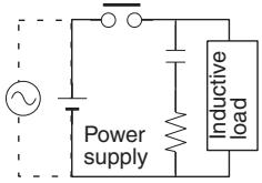 | Yes | Yes | If the load is a relay or solenoid, there is a time lag between the moment the circuit is opened and the moment the load is reset.If the supply voltage is 24 or 48 V, insert the surge protector in parallel with the load. If the supply voltage is 100 to 200 V, insert the surge protector between the contacts. | The capacitance of the capacitor must be 1 to 0.5 F per contact current of 1 A and resistance of the resistor must be 0.5 to 1 per contact voltage of 1 V. These values, however, vary with the load and the characteristics of the relay. Decide these values from testing, and take into consideration that the capacitance suppresses spark discharge when the contacts are separated and the resistance limits the current that flows into the load when the circuit is closed again.The dielectric strength of the capacitor must be 200 to 300 V. If the circuit is an AC circuit, use a capacitor with no polarity. |
Diode method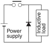 | No | Yes | The diode connected in parallel with the load changes energy accumulated by the coil into a current, which then flows into the coil so that the current will be converted into Joule heat by the resistance of the inductive load.This time lag, between the moment the circuit is opened and the moment the load is reset, caused by this method is longer than that caused by the CR method. | The reversed dielectric strength value of the diode must be at least 10 times as large as the circuit voltage value. The forward current of the diode must be the same as or larger than the load current.The reversed dielectric strength value of the diode may be two to three times larger than the supply voltage if the surge protector is applied to electronic circuits with low circuit voltages. |
Varistor method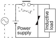 | Yes | Yes | The varistor method prevents the imposition of high voltage between the contacts by using the constant voltage characteristic of the varistor. There is time lag between the moment the circuit is opened and the moment the load is reset.If the supply voltage is 24 or 48 V, insert the varistor in parallel with the load. If the supply voltage is 100 to 200 V, insert the varistor between the contacts. | --- |
When switching a load with a high inrush current such as an incandescent lamp, suppress the inrush current as shown below.
Countermeasure 1
Providing a dark current of approx. one-third of the rated value through an incandescent lamp
Countermeasure 2
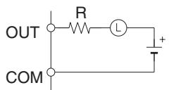
Providing a limiting resistor
SECTION 1
PC Setup and Other Features
This section explains the PC Setup and other CQM1H features, including interrupt processing and communications. The PC Setup can be used to control the operating parameters of the CQM1H. To change the PC Setup, refer to the CQM1H Operation Manual for Programming Console procedures. Refer to the CX-Programmer Operation Manual for CX-Programmer procedures.
If you are not familiar with OMRON PCs or ladder programming, you can read 1-1 PC Setup as an overview of the operating parameters available for the CQM1H, but may then want to read SECTION 3 Memory Areas, SECTION 4 Ladder-diagram Programming, and related instructions in SECTION 5 Instruction Set before completing this section.
1-1 PC Setup 2
1-1-1 Changing the PC Setup.... 2
1-1-2 Serial Communications Board Settings 3
1-1-3 PC Setup Settings 4
1-2 Inner Board Settings 9
1-2-1 Settings for a Serial Communications Board 9
1-2-2 Settings for a High-speed Counter Board.... 10
1-2-3 Settings for a Pulse I/O Board 11
1-2-4 Settings for an Absolute Encoder Interface Board.... 11
1-2-5 Settings for an Analog I/O Board.... 12
1-3 Basic PC Operation and I/O Processes 12
1-3-1 Startup Mode 12
1-3-2 Hold Bit Status 13
1-3-3 RS-232C Port Servicing Time 13
1-3-4 Peripheral Port Servicing Time.... 14
1-3-5 Minimum Cycle Time.... 14
1-3-6 Input Time Constants 14
1-3-7 High-speed Timers 15
1-3-8 DSW(87) Input Digits and Output Refresh Method.... 16
1-3-9 Peripheral Port Settings 16
1-3-10 Error Log Settings.... 17
1-4 Interrupt Functions 18
1-4-1 Types of Interrupts 18
1-4-2 Processing the Same Memory Locations with the Main Program and Interrupt Subroutines 21
1-4-3 Input Interrupts 23
1-4-4 Masking All Interrupts 30
1-4-5 Interval Timer Interrupts.... 31
1-4-6 High-speed Counter 0 Interrupts 34
1-4-7 High-speed Counter 0 Overflows/Underflows 42
1-5 Pulse Output Function.... 44
1-6 Communications Functions.... 47
1-6-1 Host Link and No-protocol Communications Settings. 48
1-6-2 Host Link Communications Settings and Procedures 51
1-6-3 No-protocol Communications Settings and Procedures....53
1-6-4 One-to-one Data Links 55
1-6-5 NT Link 1:1 Mode Communications .... 57
1-6-6 Wiring Ports 58
1-7 Calculating with Signed Binary Data 58
1-7-1 Definition of Signed Binary Data.... 58
1-7-2 Arithmetic Flags 59
1-7-3 Inputting Signed Binary Data Using Decimal Values 59
1-7-4 Using Signed-binary Expansion Instructions 60
1-7-5 Application Example Using Signed Binary Data.... 60
1-1 PC Setup
The PC Setup contains operating parameters that control CQM1H operation. To make the maximum use of CQM1H functionality when using interrupt processing and communications functions, the PC Setup may be customized according to operating conditions.
The general PC Setup settings are contained in DM 6600 to DM 6655 and the Serial Communications Board settings are contained in DM 6550 to DM 6559. Strictly speaking, the Serial Communications Board settings are part of the read-only DM area, not the PC Setup, but they are included here because they are so similar to PC Setup settings.
The PC Setup defaults are set for general operating conditions, so that the CQM1H can be used without having to change the settings. You are, however, advised to check the default values before attempting operation.
Default Values
The default values for the PC Setup are 0000 for all words. The default values for DM 6600 to DM 6655 can be reset at any time by turning ON SR 25210.

When data memory (DM) is cleared from a Programming Device, the PC Setup settings will also be cleared to all zeros.
1-1-1 Changing the PC Setup
PC Setup settings are read at various times depending on the setting, as described below.
- DM 6550 to DM 6559: Read regularly when the power is ON.
- DM 6600 to DM 6614: Read only when PC's power supply is turned ON.
- DM 6615 to DM 6644: Read only when program execution begins.
- DM 6645 to DM 6655: Read regularly when the power is ON.
Changes in the PC Setup become effective only at the times given above. The CQM1H will thus have to be restarted to make changes in DM 6600 to DM 6614 effective, and program execution will have to be restarted to make changes in DM 6615 to DM 6644 effective.
Making Changes from a Programming Device
The PC Setup can be read, but not written, from the user program. Writing can be done only by using a Programming Console or other Programming Device.
DM 6600 to DM 6644 can be set or changed only while in PROGRAM mode. DM 6550 to DM 6559 and DM 6645 to DM 6655 can be set or changed while in either PROGRAM mode or MONITOR mode.
Write-protecting the PC Setup
After PC Setup settings have been made, pin 1 on the DIP switch on the front of the CPU Unit can be turned ON to prevent Programming Devices from overwriting the PC Setup. When pin 1 is ON, the user program, the read-only DM area (DM 6144 to DM 6568), and the PC Setup (DM 6600 to DM 6655) cannot be overwritten from a Programming Device.
Errors in the PC Setup
If an incorrect PC Setup setting is accessed, a non-fatal error (error code 9B) will be generated, the corresponding error flag will be turned ON, and the default setting will be used.
| Flag(s) | Function |
| AR 2400 | Turns ON when there is an error in DM 6600 to DM 6614 (read when the power is turned ON). |
| AR 2401 | Turns ON when there is an error in DM 6615 to DM 6644 (read at the beginning of operation). |
| AR 2402 | Turns ON when there is an error in DM 6645 to DM 6655 (read regularly when power is ON). |
| AR 0400 to AR 0407 | An error code of 10 is written to this byte when there is an error in DM 6550 to DM 6559 (read regularly when power is ON). |
1-1-2 Serial Communications Board Settings
The following table shows the Serial Communications Board settings in the DM area. For details, refer to the Serial Communications Board Operation Manual.
| Word(s) | Bit(s) | Function | |||
| Serial Communications Board SettingsThe following settings are effective after transfer to the PC. (The settings for port 2 are contained in words DM 6550 to DM 6554 and the settings for port 1 are contained in words DM 6555 to DM 6559.) | |||||
| DM 6550 (port 2)DM 6555 (port 1) | 00 to 03 | Port Settings0: Standard (1 start bit, 7-bit data, even parity, 2 stop bits, 9,600 bps)1: Settings in DM 6551 (DM 6556 for port 1) | |||
| 04 to 07 | CTS Control Settings0: Disable; 1: Set | ||||
| 08 to 11 | Link Words for 1:1 Data Link (when bits 12 to 15 are set to 3)0: LR 00 to LR 63; 1: LR 00 to LR 31; 2: LR 00 to LR 15Maximum Programmable Terminal unit number (when bits 12 to 15 are set to 5)1 to 7 | ||||
| 12 to 15 | Communications Mode0: Host Link; 1: No-protocol; 2: 1:1 Data Link Slave; 3: 1:1 Data Link Master; 4: NT Link in 1:1 Mode; 5: NT Link in 1:N Mode; 6: Protocol Macro | ||||
| DM 6551 (port 2)DM 6556 (port 1) | 00 to 07 | Baud Rate00: 1.2K, 01: 2.4K, 02: 4.8K, 03: 9.6K, 04: 19.2K | |||
| 08 to 15 | Frame FormatStart Length Stop Parity00: 1bit 7 bits 1 bit Even01: 1bit 7 bits 1 bit Odd02: 1bit 7 bits 1 bit None03: 1bit 7 bits 2 bit Even04: 1bit 7 bits 2 bit Odd05: 1bit 7 bits 2 bit None06: 1 bit 8 bits 1 bit Even07: 1 bit 8 bits 1 bit Odd08: 1 bit 8 bits 1 bit None09: 1 bit 8 bits 2 bit Even10: 1 bit 8 bits 2 bit Odd11: 1 bit 8 bits 2 bit None | ||||
| DM 6552 (port 2)DM 6557 (port 1) | 00 to 15 | Transmission Delay (Host Link or No-protocol)0000 to 9999 (BCD): Set in units of 10 ms, e.g., a setting of 0001 equals 10 ms | |||
| Word(s) | Bit(s) | Function | |||
| DM 6553 (port 2)DM 6558 (port 1) | 00 to 07 | Node Number (Host Link)00 to 31 (BCD) | |||
| 08 to 11 | Start Code Enable (No-protocol)0: Disable; 1: Set | ||||
| 12 to 15 | End Code Enable (No-protocol)0: Disable (number of bytes received)1: Set (specified end code)2: CR, LF | ||||
| DM 6554 (port 2)DM 6559 (port 1) | 00 to 07 | Start Code (No-protocol)00 to FF (hexadecimal) | |||
| 08 to 15 | When bits 12 to 15 of DM 6553 or DM 6558 are set to 0:Number of Bytes Received00: Default setting (256 bytes)01 to FF: 1 to 255 bytesWhen bits 12 to 15 of DM 6553 or DM 6558 are set to 1:End Code (No-protocol)00 to FF (hexadecimal) | ||||
1-1-3 PC Setup Settings
The following table shows the PC Setup settings in order in the DM area. For details, refer to the page numbers shown.
| Word(s) | Bit(s) | Function | Page | |||
| Startup Processing (DM 6600 to DM 6614)The following settings are effective after transfer to the PC only after the PC is restarted. | ||||||
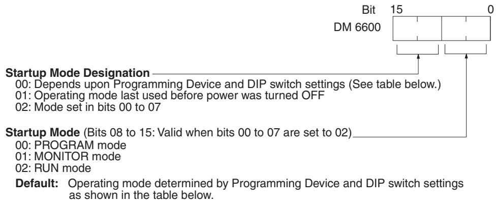
| DM 6600 | 00 to 07 | Startup Mode (effective when bits 08 to 15 are set to 02).00: PROGRAM; 01: MONITOR 02: RUN | 12 | |||
| 08 to 15 | Startup Mode Designation00: Depends on CPU Unit DIP switch pin 7 and Programming Console switch settings01: Continue operating mode last used before power was turned OFF02: Setting in DM 6600 bits 00 to 07 | |||||
| DM 6601 | 00 to 07 | Not used. | ||||
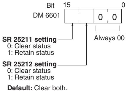
| 08 to 11 | I/O Hold Bit Status (SR 25212)0: Reset; 1: Maintain | 13 | ||||
| 12 to 15 | Forced Status Hold Bit Status (SR 25211)0: Reset; 1: Maintain | |||||
| DM 6602 to DM 6603 | 00 to 15 | Inner Board Slot 1 Settings (See 1-2 Inner Board Settings for details.) | 9 | |||
| DM 6604 to DM 6610 | 00 to 15 | Not used. | ||||
| DM 6611 to DM 6612 | 00 to 15 | Inner Board Slot 2 Settings (See 1-2 Inner Board Settings for details.) | 9 | |||
| DM 6613 | 00 to 15 | Servicing Time Setting for Serial Communications Board Port 2 | 9 | |||
| DM 6614 | 00 to 15 | Servicing Time Setting For Serial Communications Board Port 1 | ||||
| Pulse Output and Cycle Time Settings (DM 6615 to DM 6619)The following settings are effective after transfer to the PC the next time operation is started. | ||||||
| DM 6615 | 00 to 07 | Word for Pulse Output00: IR 100; 01: IR101; 02: IR 102... 15: IR 115Sets the word used for pulse output from an output on a Transistor Output Unit. Pulses can be output only from one output at a time. | 46 | |||
| 08 to 15 | Not used. Set to 00. | |||||
| Word(s) | Bit(s) | Function | Page | |||
| DM 6616 | 00 to 07 | Servicing Time for RS-232C Port (when bits 08 to 15 are set to 01)00 to 99 (BCD): Percentage of cycle time used to service RS-232C port. The servicing time must be between 0.256 ms and 65.536 ms. | 13 | |||
| 08 to 15 | RS-232C Port Servicing Setting Enable00: 5% of the cycle time01: Use time in 00 to 07.(When the PC is stopped, the servicing time will always be 10 ms.) | |||||
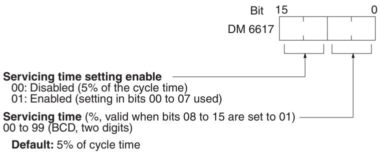
| DM 6617 | 00 to 07 | Servicing Time for Peripheral Port (when bits 08 to 15 are set to 01)00 to 99 (BCD): Percentage of cycle time used to service peripheral port. The servicing time must be between 0.256 ms and 65.536 ms. | 14 | |||
| 08 to 15 | Peripheral Port Servicing Setting Enable00: 5% of the cycle time01: Use time setting in bits 00 to 07.(When the PC is stopped, the servicing time will always be 10 ms.) | |||||
| DM 6618 | 00 to 07 | Cycle Monitor Time (when bits 08 to 15 are set to 01, 02, or 03)00 to 99 (BCD) × setting units (See bits 08 to 15.) | 17 | |||
| 08 to 15 | Cycle Monitor Enable00: 120 ms (setting in bits 00 to 07 disabled)01: Setting units: 10 ms02: Setting units: 100 ms03: Setting units: 1 s | |||||
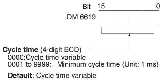
| DM 6619 | 00 to 15 | Cycle Time0000: Variable (no minimum)0001 to 9999 (BCD): Minimum cycle time in ms | 14 | |||
| Interrupt Processing (DM 6620 to DM 6639)The following settings are effective after transfer to the PC the next time operation is started. | ||||||
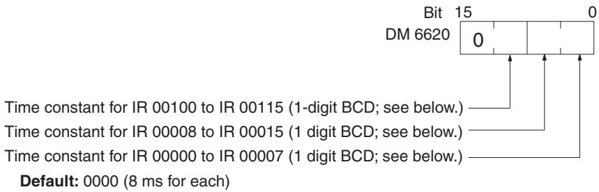
| DM 6620 | 00 to 03 | Input Time Constant for IR 00000 to IR 000070: 8 ms; 1: 1 ms; 2: 2 ms; 3: 4 ms; 4: 8 ms; 5: 16 ms; 6: 32 ms; 7: 64 ms; 8: 128 ms | 14 | |||
| 04 to 07 | Input Time Constant for IR 00008 to IR 00015 (Setting same as bits 00 to 03) | |||||
| 08 to 11 | Input Time Constant for IR 001 (Setting same as bits 00 to 03) | |||||
| 12 to 15 | Not used. Set to 0. | |||||
| DM 6621 | 00 to 07 | Input Constant for IR 00200: 8 ms; 01: 1 ms; 02: 2 ms; 03: 4 ms; 04: 8 ms; 05: 16 ms; 06: 32 ms; 07: 64 ms; 08: 128 ms | 14 | |||
| 08 to 15 | Input Constant for IR 003 (Setting same as for IR 002.) | |||||
| DM 6622 | 00 to 07 | Input Constant for IR 004 (Setting same as for IR 002.) | ||||
| 08 to 15 | Input Constant for IR 005 (Setting same as for IR 002.) | |||||
| DM 6623 | 00 to 07 | Input Constant for IR 006 (Setting same as for IR 002.) | ||||
| 08 to 15 | Input Constant for IR 007 (Setting same as for IR 002.) | |||||
| DM 6624 | 00 to 07 | Input Constant for IR 008 (Setting same as for IR 002.) | ||||
| 08 to 15 | Input Constant for IR 009 (Setting same as for IR 002.) | |||||
| DM 6625 | 00 to 07 | Input Constant for IR 010 (Setting same as for IR 002.) | ||||
| 08 to 15 | Input Constant for IR 011 (Setting same as for IR 002.) | |||||
| DM 6626 | 00 to 07 | Input Constant for IR 012 (Setting same as for IR 002.) | ||||
| 08 to 15 | Input Constant for IR 013 (Setting same as for IR 002.) | |||||
| DM 6627 | 00 to 07 | Input Constant for IR 014 (Setting same as for IR 002.) | ||||
| 08 to 15 | Input Constant for IR 015 (Setting same as for IR 002.) | |||||
| DM 6628 | 00 to 03 | Interrupt Enable for IR 000000: Normal input; 1: Interrupt input in Interrupt Input Mode or Counter Mode | 26 | |||
| 04 to 07 | Interrupt Enable for IR 000010: Normal input; 1: Interrupt input in Interrupt Input Mode or Counter Mode | |||||
| 08 to 11 | Interrupt Enable for IR 000020: Normal input; 1: Interrupt input in Interrupt Input Mode or Counter Mode | |||||
| 12 to 15 | Interrupt Enable for IR 000030: Normal input; 1: Interrupt input in Interrupt Input Mode or Counter Mode | |||||
| Word(s) | Bit(s) | Function | Page | |||
| DM 6629 | 00 to 07 | Number of TIMH(15) High-speed Timers to Refresh by Interrupt Refreshing00 to 15 (BCD; e.g., set 3 for timers 00 to 02) | 15 | |||
| 08 to 15 | High-speed Timer Interrupt Refresh Enable00: 16 timers (setting in bits 00 to 07 disabled)01: Use setting in 00 to 07 | |||||
| DM 6630 | 00 to 07 | First Input Refresh Word for I/O Interrupt 0: 00 to 11 (BCD) | 26 | |||
| 08 to 15 | Number of Input Refresh Words for I/O Interrupt 0: 00 to 12 (BCD) | |||||
| DM 6631 | 00 to 07 | First Input Refresh Word for I/O Interrupt 1: 00 to 11 (BCD) | ||||
| 08 to 15 | Number of Input Refresh Words for I/O interrupt 1: 00 to 12 (BCD) | |||||
| DM 6632 | 00 to 07 | First Input Refresh Word for I/O Interrupt 2: 00 to 11 (BCD) | ||||
| 08 to 15 | Number of Input Refresh Words for I/O Interrupt 2: 00 to 12 (BCD) | |||||
| DM 6633 | 00 to 07 | First Input Refresh Word for I/O Interrupt 3: 00 to 11 (BCD) | ||||
| 08 to 15 | Number of Input Refresh Words for I/O Interrupt 3: 00 to 12 (BCD) | |||||
| DM 6634 | 00 to 07 | First Input Refresh Word for High-speed Counter 1: 00 to 11 (BCD) | 26 | |||
| 08 to 15 | Number of Input Refresh Words for High-speed Counter 1: 00 to 12 (BCD) | |||||
| DM 6635 | 00 to 07 | First Input Refresh Word for High-speed Counter 2: 00 to 11 (BCD) | 26 | |||
| 08 to 15 | Number of Input Refresh Words for High-speed Counter 2: 00 to 12 (BCD) | |||||
| DM 6636 | 00 to 07 | First Input Refresh Word for Interval Timer 0: 00 to 15 (BCD) | 32, 39 | |||
| 08 to 15 | Number of Input Refresh Words for Interval Timer 0: 00 to 16 (BCD) | |||||
| DM 6637 | 00 to 07 | First Input Refresh Word for Interval Timer 1: 00 to 15 (BCD) | ||||
| 08 to 15 | Number of Input Refresh Words for Interval Timer 1: 00 to 16 (BCD) | |||||
| DM 6638 | 00 to 07 | First Input Refresh Word for Interval Timer 2 or High-speed Counter 0:00 to 15 (BCD) | ||||
| 08 to 15 | Number of Input Refresh Words for Interval Timer 2 or High-speed Counter 0:00 to 16 (BCD) | |||||
| DM 6639 | 00 to 07 | Output Refresh Method00: Cyclic; 01: Direct | 16, 475 | |||
| 08 to 15 | Number of Digits for DIGITAL SWITCH (DSW(87)) Instruction00: 4 digits; 01: 8 digits | 16, 427 | ||||
| High-speed Counter Settings (DM 6640 to DM 6644)The following settings are effective after transfer to the PC the next time operation is started. | ||||||
| DM 6640 toDM 6641 | 00 to 15 | Inner Board Slot 1 Settings (See 1-2 Inner Board Settings for details.) | 9 | |||
| DM 6642 | 00 to 03 | High-speed Counter 0 Input Mode0: Differential phase mode; 4: Incrementing mode | 39 | |||
| 04 to 07 | High-speed Counter 0 Reset Mode0: Phase-Z and software reset; 1: Software reset only | |||||
| 08 to 15 | High-speed Counter 0 Enable00: Don't use high-speed counter 0; 01: Use high-speed counter 0. | |||||
| DM 6643 toDM 6644 | 00 to 15 | Inner Board Slot 2 Settings (See 1-2 Inner Board Settings for details.) | 9 | |||
| Word(s) | Bit(s) | Function | Page | |||
| RS-232C Port SettingsThe following settings are effective after transfer to the PC. | ||||||
| DM 6645 | 00 to 03 | Port Settings (Host Link or No-protocol mode)0: Standard (1 start bit, 7-bit data, even parity, 2 stop bits, 9,600 bps)1: Settings in DM 6646 | 47 | |||
| 04 to 07 | CTS Control Settings (Host Link or No-protocol mode)0: Disable; 1: Set | |||||
| 08 to 11 | Link Words for 1:1 Data Link (1:1 data link master mode)0: LR 00 to LR 63; 1: LR 00 to LR 31; 2: LR 00 to LR 15 | |||||
| 12 to 15 | Communications Mode0: Host Link; 1: No-protocol; 2: 1:1 Data Link Slave; 3: 1:1 Data Link Master; 4: NT Link in 1:1 Mode | |||||
| DM 6646 | 00 to 07 | Baud Rate00: 1.2 kbps, 01: 2.4 kbps, 02: 4.8 kbps, 03: 9.6 kbps, 04: 19.2 kbps | ||||
| 08 to 15 | Frame FormatStart Length Stop Parity00: 1 bit 7 bits 1 bit Even01: 1 bit 7 bits 1 bit Odd02: 1 bit 7 bits 1 bit None03: 1 bit 7 bits 2 bit Even04: 1 bit 7 bits 2 bit Odd05: 1 bit 7 bits 2 bit None06: 1 bit 8 bits 1 bit Even07: 1 bit 8 bits 1 bit Odd08: 1 bit 8 bits 1 bit None09: 1 bit 8 bits 2 bit Even10: 1 bit 8 bits 2 bit Odd11: 1 bit 8 bits 2 bit None | |||||
| DM 6647 | 00 to 15 | Transmission Delay (Host Link or No-protocol)0000 to 9999 (BCD): Set in units of 10 ms, e.g., a setting of 0001 equals 10 ms | ||||
| DM 6648 | 00 to 07 | Node Number (Host Link): 00 to 31 (BCD) | 47 | |||
| 08 to 11 | Start Code Enable (No-protocol)0: Disable; 1: Set | |||||
| 12 to 15 | End Code Enable (No-protocol)0: Disable (number of bytes received)1: Set (specified end code)2: CR, LF | |||||
| DM 6649 | 00 to 07 | Start Code (No-protocol)00 to FF (hexadecimal) | ||||
| 08 to 15 | When bits 12 to 15 of DM 6648 are set to 0:Number of Bytes Received00: Default setting (256 bytes)01 to FF: 1 to 255 bytesWhen bits 12 to 15 of DM 6648 are set to 1:End Code (No-protocol)00 to FF (hexadecimal) | |||||
| Peripheral Port SettingsThe following settings are effective after transfer to the PC. | ||||||
| DM 6650 | 00 to 03 | Port Settings (Host Link or No-protocol mode)0: Standard (1 start bit, 7-bit data, even parity, 2 stop bits, 9,600 bps)1: Settings in DM 6651 | 16, 47 | |||
| 04 to 07 | CTS Control Settings (Host Link or No-protocol mode)0: Disable; 1: Set | |||||
| 08 to 11 | Not used. | |||||
| 12 to 15 | Communications Mode (when bits 00 to 03 are set to 1)0: Host Link; 1: No-protocolWhen a Programming Console is connected to the peripheral port, turn OFF pin 7 of the CPU Unit's DIP switch. (Pin 5 and the PC Setup settings are disabled in this case.)When connecting a personal computer to the peripheral port for use as a Programming Device, turn pin 7 ON and set the communications mode to “Host Link.” When these settings have been made and the personal computer is set for peripheral bus operation, the CPU Unit's peripheral port communications mode will automatically switch to peripheral bus mode. | |||||
| DM 6651 | 00 to 07 | Baud Rate (Host Link, peripheral bus, or No-protocol mode)00: 1.2 kbps, 01: 2.4 kbps, 02: 4.8 kbps, 03: 9.6 kbps, 04: 19.2 kbps | 47 | |||
| 08 to 15 | Frame Format (Host Link or No-protocol mode)Start Length Stop Parity00: 1 bit 7 bits 1 bit Even01: 1 bit 7 bits 1 bit Odd02: 1 bit 7 bits 1 bit None03: 1 bit 7 bits 2 bit Even04: 1 bit 7 bits 2 bit Odd05: 1 bit 7 bits 2 bit None06: 1 bit 8 bits 1 bit Even07: 1 bit 8 bits 1 bit Odd08: 1 bit 8 bits 1 bit None09: 1 bit 8 bits 2 bit Even10: 1 bit 8 bits 2 bit Odd11: 1 bit 8 bits 2 bit None | |||||
| DM 6652 | 00 to 15 | Transmission Delay (No-protocol or Slave-initiated Host Link communications only)0000 to 9999 (BCD): Set in units of 10 ms, e.g., a setting of 0001 equals 10 ms | ||||
| DM 6653 | 00 to 07 | Node Number (Host Link): 00 to 31 (BCD) | ||||
| 08 to 11 | Start Code Enable (No-protocol)0: Disable; 1: Set | |||||
| 12 to 15 | End Code Enable (No-protocol)0: Disable (number of bytes received)1: Set (specified end code)2: CR, LF | |||||
| DM 6654 | 00 to 07 | Start Code (No-protocol)00 to FF (hexadecimal) | 47 | |||
| 08 to 15 | When bits 12 to 15 of DM 6653 are set to 0:Number of Bytes Received00: Default setting (256 bytes)01 to FF: 1 to 255 bytesWhen bits 12 to 15 of DM 6653 are set to 1:End Code (No-protocol)00 to FF (hexadecimal) | |||||
| Word(s) | Bit(s) | Function | Page | |||
| Error Log Settings (DM 6655)The following settings are effective after transfer to the PC. | ||||||
| DM 6655 | 00 to 03 | Style0: Shift after 10 records have been stored1: Store only first 10 records (no shifting)2 to F: Do not store records | 17 | |||
| 04 to 07 | Not used. Set to 0. | |||||
| 08 to 11 | Cycle Time Monitor Enable0: Detect long cycles as non-fatal errors1: Do not detect long cycles | |||||
| 12 to 15 | Low Battery Error Enable0: Detect low battery voltage as non-fatal error1: Do not detect low battery voltage | |||||
1-2 Inner Board Settings
This section explains the PC Setup settings related to Inner Boards mounted in Inner Board slots 1 and 2.
1-2-1 Settings for a Serial Communications Board
Use the settings in DM 6613 and DM 6614 to set the servicing times for a Serial Communications Board mounted in Inner Board slot 1. (A Serial Communications Board cannot be mounted in slot 2.)
| Word | Bits | Function |
| DM 6613 | 00 to 07 | Servicing Time for Serial Communications Board Port 2 (enabled by bits 08 to 15)00 to 99 (BCD): Sets the percentage of the cycle time used to service port 2. The servicing time must be between 0.256 ms and 65.536 ms. |
| 08 to 15 | Serial Communications Board Port 2 Servicing Setting00: Fixed at 5% of the cycle time.01: Use time setting in bits 00 to 07.(When the PC is stopped, the servicing time will always be 10 ms.) | |
| DM 6614 | 00 to 07 | Servicing Time for Serial Communications Board Port 1 (enabled by bits 08 to 15)00 to 99 (BCD): Sets the percentage of the cycle time used to service port 1. The servicing time must be between 0.256 ms and 65.536 ms. |
| 08 to 15 | Serial Communications Board Port 1 Servicing Setting00: Fixed at 5% of the cycle time.01: Use time setting in bits 00 to 07.(When the PC is stopped, the servicing time will always be 10 ms.) |
1-2-2 Settings for a High-speed Counter Board
The settings in DM 6602, DM 6640, and DM 6641 determine the operation of a High-speed Counter Board mounted in Inner Board slot 1.
The settings in DM 6611, DM 6643, and DM 6644 determine the operation of a High-speed Counter Board mounted in Inner Board slot 2.
| Word | Bits | Function | Settings |
| DM 6602 (Slot 1)DM 6611 (Slot 2) | 00 | High-speed Counter PV Data Format | OFF: 8-digit hexadecimalON: 8-digit BCD |
| 01 to 07 | Not used | Set to 0. | |
| 08 | External Output Transistor Selector | OFF: SourcingON: Sinking | |
| 09 to 15 | Not used. | Set to 0. | |
| DM 6640 (Slot 1)DM 6643 (Slot 2) | 00 to 03 | High-speed Counter 1 Input Mode | See note 1. |
| 04 to 07 | High-speed Counter 1 Count Frequency, Numeric Range, and Counter Reset Mode | See note 2. | |
| 08 to 11 | High-speed Counter 2 Input Mode | See note 1. | |
| 12 to 15 | High-speed Counter 2 Count Frequency, Numeric Range, and Counter Reset Mode | See note 2. | |
| DM 6641 (Slot 1)DM 6644 (Slot 2) | 00 to 03 | High-speed Counter 3 Input Mode | See note 1. |
| 04 to 07 | High-speed Counter 3 Count Frequency, Numeric Range, and Counter Reset Mode | See note 2. | |
| 08 to 11 | High-speed Counter 4 Input Mode | See note 1. | |
| 12 to 15 | High-speed Counter 4 Count Frequency, Numeric Range, and Counter Reset Mode | See note 2. |
Note
- The settings for the high-speed counter input mode are as follows:
| Setting | Input Mode |
| 0 Hex | Differential Phase Inputs, 1x |
| 1 Hex | Differential Phase Inputs, 2x |
| 2 Hex | Differential Phase Inputs, 4x |
| 3 Hex | Up/Down Input |
| 4 Hex | Pulse/Direction Input |
- The settings for the high-speed counter count frequency, numeric range, and counter reset mode are as follows:
| Setting | Count frequency | Numeric range | Reset mode |
| 0 Hex | 50 kHz | Linear Counting | Phase-Z + Software Reset |
| 1 Hex | Software Reset Only | ||
| 2 Hex | Ring Counting | Phase-Z + Software Reset | |
| 3 Hex | Software Reset Only | ||
| 4 Hex | 500 kHz | Linear Counting | Phase-Z + Software Reset |
| 5 Hex | Software Reset Only | ||
| 6 Hex | Ring Counting | Phase-Z + Software Reset | |
| 7 Hex | Software Reset Only |
1-2-3 Settings for a Pulse I/O Board
The settings in DM 6611, DM 6643, and DM 6644 determine the operation of a Pulse I/O Board mounted in Inner Board slot 2. (A Pulse I/O Board cannot be mounted in slot 1.)
| Word | Bits | Function |
| DM 6611 | 00 to 15 | Mode Setting for Ports 1 and 20000: High-speed Counter Mode0001: Simple Positioning Mode |
| DM 6643 | 00 to 03 | Port 1 Input Mode0: Differential Phase Mode1: Pulse/Direction Mode2: Up/Down Mode |
| 04 to 07 | Port 1 Counter Reset Method0: Phase-Z and software reset; 1: Software reset only | |
| 08 to 11 | Port 1 Numeric Range0: Linear counting; 1: Ring counting | |
| 12 to 15 | Port 1 Pulse Output Duty Factor0: Fixed duty factor; 1: Variable duty factor | |
| DM 6644 | 00 to 03 | Port 2 Input Mode0: Differential Phase Mode1: Pulse/Direction Mode2: Up/Down Mode |
| 04 to 07 | Port 2 Counter Reset Method0: Phase-Z and software reset; 1: Software reset only | |
| 08 to 11 | Port 2 Numeric Range0: Linear counting; 1: Ring counting | |
| 12 to 15 | Port 2 Pulse Output Duty Factor0: Fixed duty factor; 1: Variable duty factor |
1-2-4 Settings for an Absolute Encoder Interface Board
The settings in DM 6611, DM 6612, DM 6643, and DM 6644 determine the operation of an Absolute Encoder Interface Board mounted in Inner Board slot 2. (An Absolute Encoder Interface Board cannot be mounted in slot 1.)
| Word | Bits | Function |
| DM 6611 | 00 to 15 | Origin Compensation for Port 1 (4-digit BCD)Origin will be compensated when the Port 1 Origin Compensation Bit (SR 25201) is turned ON. The compensation value will be recorded in BCD between 0000 and 4095 whether the counter is set to BCD mode or 360^ mode. |
| DM 6612 | 00 to 15 | Origin Compensation for Port 2 (4-digit BCD)Origin will be compensated when the Port 2 Origin Compensation Bit (SR 25202) is turned ON. The compensation value will be recorded in BCD between 0000 and 4095 whether the counter is set to BCD mode or 360^ mode. |
| DM 6643 | 00 to 07 | Port 1 Input Resolution00: 8 bits; 01: 10 bits; 02: 12 bits |
| 08 to 15 | Port 1 Operating Mode00: BCD mode; 01: 360^ mode | |
| DM 6644 | 00 to 07 | Port 2 Input Resolution00: 8 bits; 01: 10 bits; 02: 12 bits |
| 08 to 15 | Port 2 Operating Mode00: BCD mode; 01: 360^ mode |
1-2-5 Settings for an Analog I/O Board
The settings in DM 6611 determine the operation of an Analog I/O Board mounted in Inner Board slot 2. (An Analog I/O Board cannot be mounted in slot 1.)
| Word | Bits | Function | Settings |
| DM 6611 | 00 to 01 | Analog Input 1 Input Signal Range | Set the bit status of the two bits as follows:00: -10 to +10 V01: 0 to 10 V10: 0 to 5 V or0 to 20 mA |
| 02 to 03 | Analog input 2 Input Signal Range | ||
| 04 to 05 | Analog input 3 Input Signal Range | ||
| 06 to 07 | Analog input 4 Input Signal Range | ||
| 08 | Analog Input 1 Usage Selection | 0: Support (use) input.1: Do not support input. | |
| 09 | Analog Input 2 Usage Selection | ||
| 10 | Analog Input 3 Usage Selection | ||
| 11 | Analog Input 4 Usage Selection | ||
| 12 to 15 | Not used. | Set to 0. |
1-3 Basic PC Operation and I/O Processes
This section explains the PC Setup settings related to basic operation and I/O processes.
1-3-1 Startup Mode
The operating mode the PC will start in when power is turned ON can be set as shown below.
| Programming Device connected at startup | Pin 7 of the CPU Unit's DIP switch | Startup mode |
| None connected. | OFF | PROGRAM mode |
| ON | RUN mode | |
| Programming Console connected. | OFF | Operating mode set on the Programming Console's mode switch |
| ON | PROGRAM mode (See note 1.) | |
| Other Programming Device connected. | OFF | PROGRAM mode (See note 1.) |
| ON | Depends upon the Connecting Cable being used. (See note 2.) |
Note
-
In these cases, the CQM1H will not be able to communicate with the connected Programming Device.
-
The startup mode will be PROGRAM mode or RUN mode, depending on the Connecting Cable being used.
| Connecting Cable | Startup mode |
| CS1W-CN114 + CQM1-CIF01/02 | PROGRAM mode |
| CS1W-CN118 + XW2Z-200/500S(-V) | PROGRAM mode |
| CS1W-CN226/626 | RUN mode |
| CS1W-CN118 + XW2Z-200/500S-CV | RUN mode |
1-3-2 Hold Bit Status
Make the settings shown below to determine whether, when the power supply is turned ON, the Forced Status Hold Bit (SR 25211) and/or I/O Hold Bit (SR 25212) will retain the status that was in effect when the power was last turned OFF, or whether the previous status will be cleared.
The Forced Status Hold Bit (SR 25211) determines whether or not the forced set/reset status is retained when changing from PROGRAM mode to MONITOR mode.
The I/O Hold Bit (SR 25212) determines whether or not the status of IR bits and LR bits is retained when PC operation is started and stopped.
1-3-3 RS-232C Port Servicing Time
The following settings are used to determine the percentage of the cycle time devoted to servicing the RS-232C port.

Example: If DM 6616 is set to 0110, the RS-232C port will be serviced for 10% of the cycle time.
The minimum servicing time is 0.256 ms.
The entire servicing time will not be used unless processing requests exist.
1-3-4 Peripheral Port Servicing Time
The following settings are used to determine the percentage of the cycle time devoted to servicing the peripheral port.
Example: If DM 6617 is set to 0115, the peripheral port will be serviced for 15% of the cycle time.
The minimum servicing time is 0.256 ms.
The entire servicing time will not be used unless processing requests exist.
1-3-5 Minimum Cycle Time
Make the settings shown below to standardize the cycle time and to eliminate variations in I/O response time by setting a minimum cycle time.
If the actual cycle time is shorter than the minimum cycle time, execution will wait until the minimum time has expired. If the actual cycle time is longer than the minimum cycle time, then operation will proceed according to the actual cycle time. AR 2405 will turn ON if the minimum cycle time is exceeded.
1-3-6 Input Time Constants
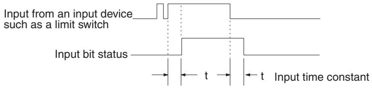
Make the settings shown below to set the time from when the actual inputs from the DC Input Unit are turned ON or OFF until the corresponding input bits are updated (i.e., until their ON/OFF status is changed). Make these settings when you want to adjust the time until inputs stabilize.
Increasing the input time constant can reduce the effects from chattering and external noise.
Input Time Constants for IR 000 and IR 001
Input Time Constants for IR 002 to IR 015
DM 6621: IR 002 and IR 003
DM 6622: IR 004 and IR 005
DM 6623: IR 006 and IR 007
DM 6624: IR 008 and IR 009
DM 6625: IR 010 and IR 011
DM 6626: IR 012 and IR 013
DM 6627: IR 014 and IR 015
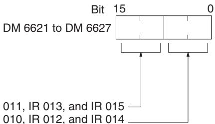
Time constant for IR 003, IR 005, IR 007, IR 009, IR 011, IR 013, and IR 015
Time constant for IR 002, IR 004, IR 006, IR 008, IR 010, IR 012, and IR 014
Default: 0000 (8 ms for each)
The nine possible settings for the input time constant are shown below. Set only the rightmost digit for IR 000.
0: 8 ms 1: 1 ms 2: 2 ms 3: 4 ms 4: 8 ms
5: 16 ms 6: 32 ms 7: 64 ms 8: 128 ms
1-3-7 High-speed Timers
Make the settings shown below to set the number of high-speed timers created with TIMH(15) that will use interrupt processing.
Default: Interrupt processing for all high-speed timers, TIM 000 to TIM 015.
The setting indicates the number of timers that will use interrupt processing beginning with TIM 000. For example, if “0108” is specified, then eight timers, TIM 000 to TIM 007 will use interrupt processing.
Note
-
High-speed timers will not be accurate without interrupt processing unless the cycle time is 10 ms or less.
-
If the SPED(64) instruction is used and pulses are output at a frequency of 500 Hz or greater, then set the number of high-speed timers with interrupt processing to four or less. Refer to information on the SPED(64) instruction for details.
-
Interrupt response time for other interrupts will be improved if interrupt processing is set to 00 when high-speed timer processing is not required. This includes any time the cycle time is less than 10 ms.
1-3-8 DSW(87) Input Digits and Output Refresh Method
Make the settings shown below to set the number of input digits for the DSW(87) instruction, and to set the output refresh method.
Default: The number of input digits for the DSW(87) instruction is set to "4" and the output refresh method is cyclic.
Refer to page 427 for details on the DSW(87) instruction and to SECTION 7 CPU Unit Operation and Processing Time for details on I/O refresh methods.
1-3-9 Peripheral Port Settings
Serial communications settings for the peripheral port are determined by pins 5 and 7 of the CPU Unit's DIP switch, the hexadecimal setting in DM 6650, and the device connected to the peripheral port.
| DIP switch settings | DM 6650 setting | Connected device | Serial communications mode | |
| Pin 5 | Pin 7 | |||
| OFF | OFF | Ignored | Programming Console | Programming Console bus |
| OFF | ON | 0000 | Programming Device other than a Programming Console (such as a personal computer) | Host Link, standard settings Peripheral bus mode if CX-Programmer is set for peripheral bus. |
| 0001 | Host Link, custom settings Peripheral bus mode if CX-Programmer is set for peripheral bus. | |||
| 10□□ | No-protocol | |||
| ON | OFF | Ignored | Programming Console | Programming Console bus |
| ON | ON | Ignored | Programming Device other than a Programming Console (such as a personal computer) | Host Link, standard settings Peripheral bus mode if CX-Programmer is set for peripheral bus. |
1-3-10 Error Log Settings
Cycle Monitor Time (DM 6618)
Make the settings shown below for detecting errors and storing the error log.
The cycle monitor time is used for checking for extremely long cycle times, as can happen when the program goes into an infinite loop. If the cycle time exceeds the cycle monitor setting, a fatal error (FALS 9F) will be generated.
Default: 120 ms.
Note
- The units used for the maximum and current cycle times recorded in AR 26 and AR 27 (4-digit BCD) depend on the unit set for the cycle monitor time in DM 6618, as shown below.
Bits 08 to 15 set to 01: 0.1 ms
Bits 08 to 15 set to 02: 1 ms
Bits 08 to 15 set to 03: 10 ms
- If the cycle time is 1 s or longer, the cycle time read from Programming Devices will be 999.9 ms. The correct maximum and current cycle times will be recorded in the AR area.
Example
If 0230 is set in DM 6618, an FALS 9F error will not occur until the cycle time exceeds 3 s. If the actual cycle time is 2.59 s, the current cycle time stored in the AR area will be 2590 (ms), but the cycle time read from a Programming Device will be 999.9 ms.
A “cycle time over” error (non-fatal) will be generated when the cycle time exceeds 100 ms unless detection of long cycle times is disable using the setting in DM 6655.
Error Detection and Error Log Operation (DM 6655)
Make the settings shown below to determine whether or not a non-fatal error is to be generated when the cycle time exceeds 100 ms or when the voltage of the built-in battery drops, and to set the method for storing records in the error log when errors occur.
Battery errors and cycle time overrun errors are non-fatal errors. For details on the error log, refer to SECTION 8 Troubleshooting.
1-4 Interrupt Functions
This section explains the settings and methods for using the CQM1H interrupt functions.
1-4-1 Types of Interrupts
The CQM1H has four types of interrupts, as outlined below.
Input Interrupts:
Interrupt processing is executed when an input from an external source to one of CPU Unit bits IR 00000 to IR 00003 turns ON.
Interval Timer Interrupts:
Interrupt processing is executed by an interval timer with a precision of 0.1 ms.
High-speed Counter Interrupts:
Interrupt processing is executed according to the present value (PV) of the built-in high-speed counter. CQM1H CPU Units are equipped with the following 3 types of high-speed counter interrupts. All can function as target-value interrupts or range-comparison interrupts. (A target-value interrupt is generated when the PV matches the SV, and a range-comparison interrupt is generated when the PV is within a preset SV range.)
1,2,3...
- High-speed counter 0 (built into the CPU Unit)
High-speed counter 0 counts pulse inputs to CPU Unit inputs 4 to 6. Two-phase pulses up to 2.5 kHz can be counted. - High-speed counters 1 and 2 (Pulse I/O Board)
High-speed counters 1 and 2 count high-speed pulse inputs to ports 1 and 2 on the Pulse I/O Board. Two-phase pulses up to 25 kHz can be counted. - Absolute high-speed counters 1 and 2 (Absolute Encoder Interface Board) High-speed counters 1 and 2 count absolute rotary encoder codes input to ports 1 and 2 on the Absolute Encoder Interface Board.
Note Interrupt processing is not performed for high-speed counters 1, 2, 3, and 4 on a High-speed Counter Board. A High-speed Counter Board can count pulses up to 50 kHz or 500 kHz. The high-speed counter PVs can be checked against a target value or an SV range and a bit pattern can be output internally or externally instead of generating an interrupt.
Serial Communications Board Interrupts:
Interrupt processing is requested from the CPU Unit when the Serial Communications Board receives the desired message.
Interrupt Processing
When an interrupt is generated, the specified interrupt subroutine is executed.
Defining Subroutines
Just as with ordinary subroutines, interrupt subroutines are defined using SBN(92) and RET(93) at the end of the main program.
When interrupt subroutines are executed, a specified range of input bits can be refreshed.
When an interrupt subroutine is defined, a “no SBS error” will be generated during the program check but execution will proceed normally. If this error occurs, check all normal subroutines to be sure that SBS(91) has been programmed before proceeding.
Interrupt Priority
Interrupts have the following order of priority. Input interrupts and interrupts from high-speed counters 1 and 2 have the highest priority and the interrupt notification from a Serial Communications Board has the lowest.
$$ \boxed {\text {Input}} _ {\text {interrupts}} = \boxed {\text {High - speed counter 1 or 2 interrupts (from Pulse I/O Board or Absolute Encoder Interface Board)}} > \boxed {\text {Interval timer interrupts}} = \boxed {\text {High - speed counter 0 interrupt}} > \boxed {\text {Interrupt notification from Serial Communications Board}} $$
When an interrupt with a higher priority is received during interrupt processing, the current processes will be stopped and the newly received interrupt will be processed instead. After that routine has been completely executed, then processing of the previous interrupt will be resumed.
When an interrupt with a lower or equal priority is received during interrupt processing, then the newly received interrupt will be processed as soon as the routine currently being processed has been completely executed.
If two interrupts with the same priority level occur simultaneously, the interrupts will be executed in the following order:
1,2,3...
- Input interrupt 0 > Input interrupt 1 > Input interrupt 2 > Input interrupt 3 > High-speed counter interrupt 1 > High-speed counter interrupt 2
- Interval timer interrupt 0 > Interval timer interrupt 1 > Interval timer interrupt 2 (Interval timer interrupt 2 is high-speed counter interrupt 0.)
Pulse Output Instructions and Interrupts
The following instructions cannot be executed in an interrupt subroutine when an instruction that controls pulse I/O or high-speed counters is being executed in the main program: (SR 25503 turns ON)
INI(89), PRV(62), CTBL(63), SPED(64), PULS(65), PWM(—), PLS2(—) and ACC(—)
The following methods can be used to circumvent this limitation:
Method 1
All interrupt processing can be masked while the instruction is being executed.
flowchart
graph TD
    A["Power Supply"] --> B["@INT(89)"]
    B --> C["100"]
    B --> D["000"]
    B --> E["000"]
    F["@PLS2(---)"] --> G["001"]
    F --> H["000"]
    F --> I["DM 0010"]
    J["@INT(89)"] --> K["200"]
    J --> L["000"]
    J --> M["000"]
Method 2
Execute the instruction again in the main program.
This is the program section from the main program:
flowchart
graph TD
    A["Start"] --> B["@PRV(62)"]
    B --> C["001"]
    B --> D["002"]
    B --> E["DM 0000"]
    F["Start"] --> G["@CTBL(63)"]
    G --> H["001"]
    G --> I["000"]
    G --> J["DM 0000"]
    G --> K["RSET LR 0000"]
This is the program section from the interrupt subroutine:
1-4-2 Processing the Same Memory Locations with the Main Program and Interrupt Subroutines
If a memory location is manipulated both by the main program and an interrupt subroutine, an interrupt mask must be set to disable interrupts.
When an interrupt occurs, execution of the main program will be interrupted immediately, even during execution of an instruction. The intermediate processing results is saved for use after completing the interrupt subroutine, i.e., when the interrupt subroutine has been executed, execution of the main program is started from the same position with data restored to the previous condition. If any of the memory locations being used by the main program are changed in the interrupt subroutine, the changes will be lost when data is restored to the previous state when restarting execution of the main program. It is thus necessary to disable interrupts before and enable interrupts after any instructions that should be executed to completion even if an interrupt occurs.
Processing Interrupted between 1st and 3rd Operands
flowchart
graph LR
    A["Main Program"] --> B{ADD}
    B --> C["DM0000"]
    B --> D["#0001"]
    B --> E["DM0000"]
    F["Interrupt Subroutine"] --> G{MOV}
    G --> H["#0010"]
    G --> I["DM0000"]
    G --> J{ }
Flow of Processing

flowchart
graph TD
    A["Status of DM 0000 read. 1234"] --> B["BCD addition performed. 1234+1=1235"]
    B --> C["Processing interrupted."]
    C --> D{Interrupt occurs}
    D -->|Yes| E["#0010 moved to DM 0000."]
    E --> F["Interrupt processing completed."]
    F --> G{MOV executed.}
    G -->|Yes| H["0010"]
    G -->|No| I["1234"]
    C -->|No| J["Data saved."]
    J --> K["Addition results data (1235)"]
    K --> L["Data restored."]
    L --> M["Processing continued."]
    M --> N["Addition results (1235) written."]
    N --> O["1235"]
    style A fill:#f9f,stroke:#333
    style O fill:#f9f,stroke:#333
When the interrupt occurs while processing ADD, the addition result, 1235, is saved temporarily in memory and not stored in DM 0000. Although #0010 is moved to DM 0000 in the interrupt program, the addition result that was saved is written to DM 0000 as soon as processing returns to the main program, effectively undoing the results of the interrupt program.
Countermeasure for Above Problem
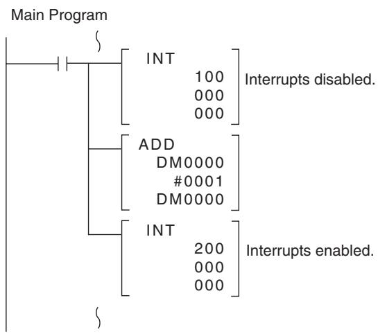
flowchart
graph TD
    A["Main Program"] --> B{ }
    B --> C["INT"]
    C --> D["100"]
    C --> E["000"]
    C --> F["000"]
    B --> G["ADD"]
    G --> H["DM0000"]
    G --> I["#0001"]
    G --> J["DM0000"]
    B --> K["INT"]
    K --> L["200"]
    K --> M["000"]
    K --> N["000"]
    B --> O["Interrupts enabled."]
Interrupting Writing
Multiple Words of Data
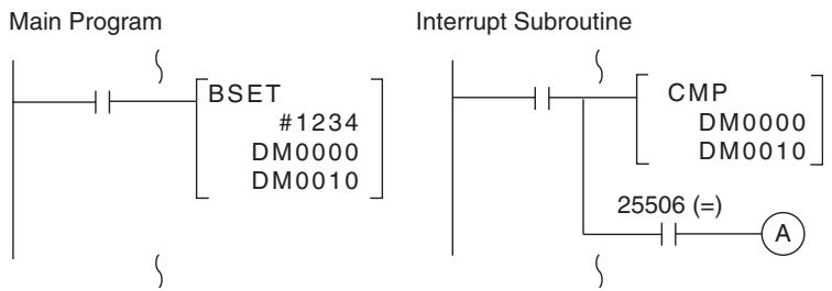
flowchart
graph TD
    A["Main Program"] --> B["BSET"]
    B --> C["#1234"]
    B --> D["DM0000"]
    B --> E["DM0010"]
    F["Interrupt Subroutine"] --> G["CMP"]
    G --> H["DM0000"]
    G --> I["DM0010"]
    J["25506 (=)"] --> K["A"]
Flow of Processing
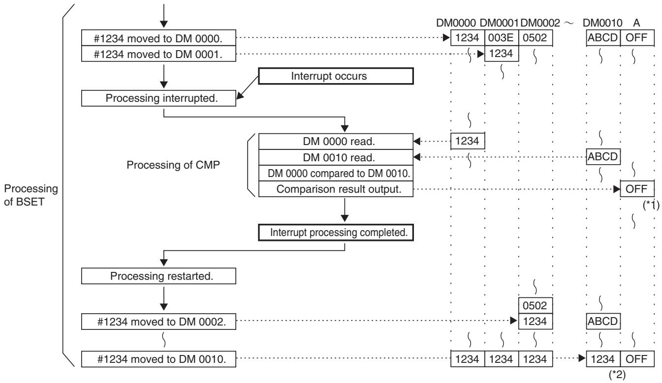
flowchart
graph TD
    A["#1234 moved to DM 0000."] --> B["Processing interrupted."]
    C["#1234 moved to DM 0001."] --> B
    B --> D["Interrupt occurs"]
    D --> E["Processing of CMP"]
    E --> F["DM 0000 read."]
    E --> G["DM 0010 read."]
    E --> H["DM 0000 compared to DM 0010."]
    E --> I["Comparison result output."]
    I --> J["Interrupt processing completed."]
    J --> K["Processing restarted."]
    K --> L["#1234 moved to DM 0002."]
    K --> M["#1234 moved to DM 0010."]
    L --> N["0502"]
    M --> O["1234"]
    N --> P["1234"]
    O --> Q["1234"]
    P --> R["1234"]
    Q --> S["1234"]
    R --> T["1234"]
    S --> U["1234"]
    T --> V["1234"]
    U --> W["1234"]
    V --> X["1234"]
    W --> Y["1234"]
    X --> Z["1234"]
    Y --> AA["1234"]
    Z --> AB["1234"]
    AA --> AC["1234"]
    AB --> AD["1234"]
    AC --> AE["1234"]
    AD --> AF["1234"]
    AE --> AG["1234"]
    AF --> AH["1234"]
    AG --> AI["1234"]
    AH --> AJ["1234"]
    AI --> AK["1234"]
    AJ --> AL["1234"]
    AK --> AM["1234"]
    AL --> AN["1234"]
    AM --> AO["1234"]
    AN --> AP["1234"]
Processing was interrupted for BSET when #1234 was not yet written to DM 0010. Therefore, in the comparison at point *1, the contents of DM 0000 and DM 0001 are not equal and processing stops with A in the OFF state. As a result, although the contents of DM 0000 and DM 0010 agree at the value
1234, an incorrect comparison result is reflected in comparison result output A.
Countermeasure for Above Problem
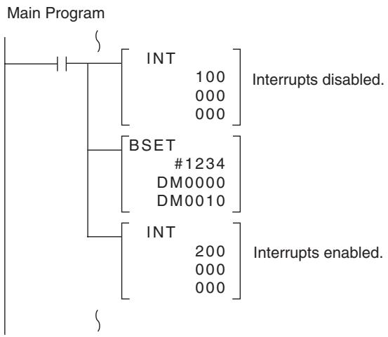
flowchart
graph TD
    A["Main Program"] --> B{ }
    B --> C["INT"]
    C --> D["100"]
    C --> E["000"]
    C --> F["000"]
    B --> G["BSET"]
    G --> H["#1234"]
    G --> I["DM0000"]
    G --> J["DM0010"]
    B --> K["INT"]
    K --> L["200"]
    K --> M["000"]
    K --> N["000"]
    B --> O{ }
    O --> P["Interrupts disabled."]
    O --> Q["Interrupts enabled."]
1-4-3 Input Interrupts
The CPU Unit's inputs allocated IR 00000 to IR 00003 can be used for interrupts from external sources. Input interrupts 0 through 3 correspond respectively to these bits and are always used to call subroutines 000 through 003 respectively. When input interrupts are not used, subroutines 000 to 003 can be used for ordinary subroutines.
Processing
There are two modes for processing input interrupts. The first is the Input Interrupt Mode, in which the interrupt is carried out in response to an external input. The second is the Counter Mode, in which signals from an external source are counted at high speed, and an interrupt is carried out once for every certain number of signals.
The INT(89) instruction determines which mode is used.
In the Input Interrupt Mode, signals with a length of 100 s or more can be detected. In the Counter Mode, signals up to 1 kHz can be counted.
Procedure (Input Interrupt Mode)
Follow the steps outlined below when using input interrupts in input interrupt mode.
1,2,3...
- Determine the input interrupt number.
| Terminal | Corresponding bit address | Subroutine number | |
| B0 | IN0 | IR 00000 | 000 |
| A0 | IN1 | IR 00001 | 001 |
| B1 | IN2 | IR 00002 | 002 |
| A1 | IN3 | IR 00003 | 003 |
- Wire the input. (See page 25 for more details.)
- Make PC Setup settings. (See page 26 for more details.)
a) Write 1 in the corresponding digit in DM 6628 to indicate that the input will be used as an input interrupt (input interrupt or counter mode.)
b) Bits in DM 6630 through DM 6633 can be turned ON to cause the input to be refreshed before the interrupt subroutine is executed.
- Program the associated program sections.
a) Use INT(89) to unmask the input interrupt. (See page 27 for more details.)
b) Write an interrupt subroutine within SBN(92) and RET(93).
flowchart
graph TD
    A["Input interrupt 0"] --> B["Interrupt 0"]
    C["1"] --> B
    D["2"] --> B
    E["3"] --> B
    B --> F["Ladder Program"]
    F --> G["Interrupt Subroutine"]
    G --> H["Generate interrupt."]
    F --> I["Interrupt 1"]
    F --> J["Interrupt 2"]
    F --> K["Interrupt 3"]
    I --> L["PC Setup"]
    J --> L
    K --> L
    L --> M["DM 6628"]
    N["00000"] --> B
    O["00001"] --> B
    P["00002"] --> B
    Q["00003"] --> B
    R["Interrupt 1"] --> F
    S["Interrupt 2"] --> F
    T["Interrupt 3"] --> F
    U["INT(89)"] --> F
    V["INTERRUPT CONTROL Enable interrupts."] --> F
    W["SBN(92)"] --> G
    X["RET(93)"] --> G
    Y["Execute specified subroutine."] --> G
Procedure (Counter Mode)
Follow the steps outlined below when using input interrupts in counter mode.
1,2,3... 1. Determine the input interrupt number.
| Terminal | Corresponding bit address | Subroutine number | |
| B0 | IN0 | IR 00000 | 000 |
| A0 | IN1 | IR 00001 | 001 |
| B1 | IN2 | IR 00002 | 002 |
| A1 | IN3 | IR 00003 | 003 |
- Determine the initial count SV.
- Wire the input. (See page 25 for more details.)
- Make PC Setup settings. (See page 26 for more details.)
a) Write 1 in the corresponding digit in DM 6628 to indicate that the input will be used as an input interrupt (input interrupt or counter mode.)
b) Bits in DM 6630 through DM 6633 can be turned ON to cause the input to be refreshed before the interrupt subroutine is executed.
- Program the associated program sections.
a) Use INT(89) to refresh the counter SV in counter mode. (See page 28 for more details.)
b) Write an interrupt subroutine within SBN(92) and RET(93) (only when using count-up interrupts.)
flowchart
graph TD
    A["Input interrupt 0"] --> B["Counter 0"]
    C["Input interrupt 1"] --> B
    D["Input interrupt 2"] --> B
    E["Input interrupt 3"] --> B
    B --> F["Input interrupt (counter mode)"]
    F --> G["Generate interrupt."]
    G --> H["Subroutine"]
    H --> I["Execute specified subroutine."]
    J["PC Setup DM 6628"] --> K["Counter 1"]
    J --> L["Counter 2"]
    J --> M["Counter 3"]
    K --> N["Ladder Program"]
    L --> N
    M --> N
    N --> O["Interrupt Control"]
    O --> P["Refresh counter SV (decrementing mode)."]
    P --> Q["Counter SV"]
    Q --> R["Counter 0: SR 244"]
    Q --> S["Counter 1: SR 245"]
    Q --> T["Counter 2: SR 246"]
    Q --> U["Counter 3: SR 247"]
    V["Each cycle"] --> W["Counter PV - 1"]
    W --> X["Counter 0: SR 248"]
    W --> Y["Counter 1: SR 249"]
    W --> Z["Counter 2: SR 250"]
    W --> AA["Counter 3: SR 251"]
    AB["Only when using interrupts."] --> AC["SBN(92)"]
    AD["RET(93)"] --> AE["RET(93)"]
Wiring Inputs
Before using input interrupts, wire the input interrupt signal or count input signal to the CPU Unit's input terminal as shown below.
Interrupt Input Signal (Input Interrupt Mode) Wiring Example
| Terminal | Corresponding bit address |
| B0 (IN0) | IR 00000 |
| A0 (IN1) | IR 00001 |
| B1 (IN2) | IR 00002 |
| A1 (IN3) | IR 00003 |

Count Input Signal (Counter Mode) Wiring Example
| Terminal | Corresponding bit address | Decrementing mode |
| B0 (IN0) | IR 00000 | Pulse inputs (4 inputs max.) |
| A0 (IN1) | IR 00001 | |
| B1 (IN2) | IR 00002 | |
| A1 (IN3) | IR 00003 |
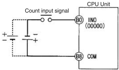
PC Setup Parameters
Before executing the program, make the following settings in the PC Setup in PROGRAM mode.
Interrupt Input Settings (DM 6628)
If these settings are not made, interrupts cannot be used in the program.
0: Normal input
1: Interrupt input
Default: All normal inputs.
Input Refresh Word Settings (DM 6630 to DM 6633)
Make these settings when it is necessary to refresh inputs for input interrupt or counter mode.
Example
If DM 6630 is set to 0100, IR 000 will be refreshed when a signal is received for interrupt 0.
Note If input refreshing is not used, input signal status within the interrupt routine will not be reliable. This includes even the status of the interrupt input bit that activated the interrupt. For example, IR 00000 would not be ON in interrupt
routine for input interrupt 0 unless it was refreshed (in this case, the Always ON Flag, SR 25313 could be used in place of IR 00000).
Input Interrupt Mode
Use the following instructions to program input interrupts using the Input Interrupt Mode.
Masking of Interrupts
With the INT(89) instruction, set or clear input interrupt masks as required.
Make the settings with the D bits 0 to 3, which correspond to input interrupts 0 to 3.
0: Mask cleared. (Input interrupt permitted.)
1: Mask set. (Input interrupt not permitted.)
At the beginning of operation, all of the input interrupts are masked. Use INT(89) to unmask input interrupts before using input interrupts in input interrupt mode.
Clearing Masked Interrupts
If the bit corresponding to an input interrupt turns ON while masked, that input interrupt will be saved in memory and will be executed as soon as the mask is cleared. In order for that input interrupt not to be executed when the mask is cleared, the interrupt must be cleared from memory.
Only one interrupt signal will be saved in memory for each interrupt number.
With the INT(89) instruction, clear the input interrupt from memory.
If D bits 0 to 3, which correspond to input interrupts 0 to 3, are set to "1," then the input interrupts will be cleared from memory.
0: Input interrupt retained.
1: Input interrupt cleared.
Reading Mask Status
With the INT(89) instruction, read the input interrupt mask status.
The status of the rightmost digit of the data stored in word D (bits 0 to 3) show the mask status.
0: Mask cleared. (Input interrupt permitted.)
1: Mask set. (Input interrupt not permitted.)
Counter Mode
Use the following steps to program input interrupts using the Input Interrupt Mode.
Note The SR words used in the Counter Mode (SR 244 to SR 251) all contain binary (hexadecimal) data (not BCD).
1,2,3...
- Write the set values for counter operation to SR words correspond to interrupts 0 to 3. The set values are written between 0000 and FFFF (0 to 65,535). A value of 0000 will disable the count operation until a new value is set and step 2, below, is repeated.
Note These SR bits are cleared at the beginning of operation, and must be written from the program.
That maximum input signal that can be counted is 1 kHz.
| Interrupt | Word containing counter SV |
| Input interrupt 0 | SR 244 |
| Input interrupt 1 | SR 245 |
| Input interrupt 2 | SR 246 |
| Input interrupt 3 | SR 247 |
If the Counter Mode is not used, these SR bits can be used as work bits.
- With the INT(89) instruction, refresh the Counter Mode set value and enable interrupts.
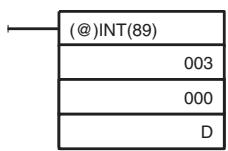
If D bits 0 to 3, which correspond to input interrupts 0 to 3, are set to "0," then the set value will be refreshed and interrupts will be permitted.
0: Counter mode set value refreshed and mask cleared. 1: Nothing happens. (Set to 1 the bits for all interrupts that are not being changed.)
The input interrupt for which the set value is refreshed will be enabled in Counter Mode. When the counter reaches the set value, an interrupt will occur, the counter will be reset, and counting/interrupts will continue until the counter is stopped.
Note
- If the INT(89) instruction is used during counting, the present value (PV) will return to the set value (SV). You must, therefore, use the differentiated form of the instruction or an interrupt may never occur.
- The set value will be set when the INT(89) instruction is executed. If interrupts are already in operation, then the set value will not be changed just by changing the content of SR 244 to SR 247, i.e., if the contents is changed, the set value must be refreshed by executing the INT(89) instruction again.
Interrupts can be masked using the same process as for the Input Interrupt Mode, but if the masks are cleared using the same process, the Counter Mode will not be maintained and the Input Interrupt Mode will be used instead. Interrupt signals received for masked interrupts can also be cleared using the same process as for the Input Interrupt Mode.
Counter PV in Counter Mode
When input interrupts are used in Counter Mode, the counter PV will be stored in the SR word corresponding to input interrupts 0 to 3. Values are 0000 to FFFE (0 to 65,534) and will equal the counter PV minus one.
| Interrupt | Word containing counter PV – 1 |
| Input interrupt 0 | SR 248 |
| Input interrupt 1 | SR 249 |
| Input interrupt 2 | SR 250 |
| Input interrupt 3 | SR 251 |
Example: The present value for an interrupt whose set value is 000A will be recorded as 0009 immediately after INT(89) is executed.
Note Even if input interrupts are not used in Counter Mode, these SR bits cannot be used as work bits.
Application Example
In this example, input interrupt 0 is used in Input Interrupt Mode and input interrupt 1 is used in Counter Mode. Before executing the program, check to be sure the PC Setup.
PC Setup: DM 6628: 0011 (IR 00000 and IR 00001 used for input interrupts) The default settings are used for all other PC Setup parameters. (Inputs are not refreshed at the time of interrupt processing.)
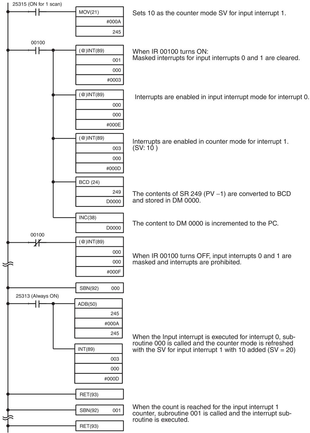
flowchart
graph TD
    A["25315 (ON for 1 scan)"] --> B["MOV(21)"]
    B --> C["#000A"]
    B --> D["245"]
    E["00100"] --> F["@INT(89)"]
    F --> G["001"]
    F --> H["000"]
    F --> I["#0003"]
    J["00100"] --> K["@INT(89)"]
    K --> L["000"]
    K --> M["000"]
    K --> N["#000E"]
    O["00100"] --> P["@INT(89)"]
    P --> Q["003"]
    P --> R["000"]
    P --> S["#000D"]
    T["BCD (24)"] --> U["249"]
    U --> V["D0000"]
    W["INC(38)"] --> X["D0000"]
    Y["00100"] --> Z["@INT(89)"]
    Z --> AA["000"]
    Z --> AB["#000F"]
    AC["25313 (Always ON)"] --> AD["SBN(92)"]
    AD --> AE["000"]
    AF["ADB(50)"] --> AG["245"]
    AH["#000A"] --> AI["245"]
    AJ["INT(89)"] --> AK["003"]
    AL["#000D"] --> AM["RET(93)"]
    AN["SBN(92)"] --> AO["001"]
    AP["RET(93)"] --> AQ["RET(93)"]

    style A fill:#f9f,stroke:#333
    style E fill:#f9f,stroke:#333
    style J fill:#f9f,stroke:#333
    style W fill:#f9f,stroke:#333
    style AC fill:#f9f,stroke:#333
    style AF fill:#f9f,stroke:#333
    style AN fill:#f9f,stroke:#333
When the program is executed, operation will be as shown in the following diagram.
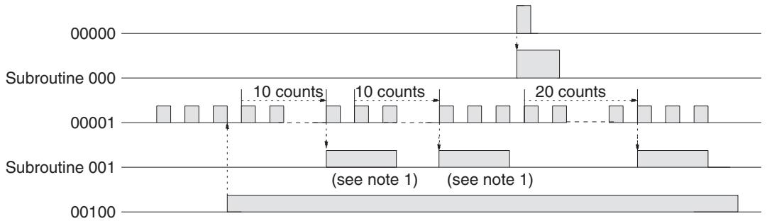
bar
| Subroutine | Count | | ---------- | ----- | | 00000 | 20 | | 00011 | 10 | | 00100 | 10 |(see note 2)
Note 1. The counter will continue operating even while the interrupt routine is being executed.
- The input interrupt will remain masked.
1-4-4 Masking All Interrupts
The INT(89) instruction can be used to mask and unmask all interrupts as a group, including input interrupts, interval timer interrupts, and high-speed counter interrupts. The mask is in addition to any masks on the individual types of interrupts. Furthermore, clearing the masks for all interrupts does not clear the masks on the individual types of interrupts, but restores them to the masked conditions that existed before INT(89) was executed to mask them as a group.
| Interrupts masked/unmasked by INT(89) | Source Unit or Board |
| Input interrupts | CPU Unit |
| Interval timer interrupts | |
| High-speed counter 0 interrupt | |
| High-speed counter 1 and 2 interrupts | Pulse I/O Board |
| High-speed counter 1 and 2 interrupts | Absolute Encoder Interface Board |
Do not use INT(89) to mask interrupts unless it is necessary to temporarily mask all interrupts and always use INT(89) instructions in pairs to do so, using the first INT(89) instruction to mask and the second one to unmask interrupts.
INT(89) cannot be used to mask and unmask all interrupts from within interrupt routines.
Masking Interrupts
Use the INT(89) instruction to disable all interrupts.
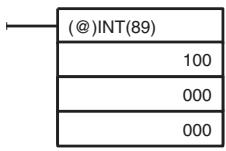
If an interrupt is generated while interrupts are masked, interrupt processing will not be executed but the interrupt will be recorded for the input, interval timer, and high-speed counter interrupts. The interrupts will then be serviced as soon as interrupts are unmasked.
Unmasking Interrupts
Use the INT(89) instruction to unmask interrupts as follows:
1-4-5 Interval Timer Interrupts
High-speed, high-precision timer interrupt processing can be executed using interval timers. The CQM1H provides three interval timers, numbered from 0 to 2.
Note
- Interval timer 0 cannot be used when pulses are being output to a Transistor Output Unit by means of the SPED(64) instruction.
- Interval timer 2 cannot be used at the same time as high-speed counter 0.
Processing
There are two modes for interval timer operation, the One-shot Mode, in which only one interrupt will be executed when time expires, and the Scheduled Interrupt Mode in which the interrupt is repeated at a fixed interval.
Procedure
Follow the steps outlined below when using interval timer interrupts.
1,2,3...
- Determine whether the timer will operate in one-shot mode or scheduled interrupt mode.
- Program the associated program sections.
a) Use STIM(69) to set the timer SV and start the timer in one-shot or scheduled interrupt mode.
b) Write an interrupt subroutine within SBN(92) and RET(93).
flowchart
graph TD
    A["Interval timers 0 to 3\n(See notes 1 and 2.)"] --> B["Generate interrupt."]
    C["Ladder Program"] --> D["INTerval TIMER\nStart the timer.\nOne-shot mode\nScheduled interrupt mode\nRead elapsed time."]
    D --> E["Execute specified subroutine."]
    E --> F["SBN(92)"]
    E --> G["RET(93)"]
Note
- Interval timer 2 and high-speed counter 0 cannot be used at the same time.
- Interval timer 0 cannot be used at the same time as pulse outputs from Transistor Output Units produced by SPED(64).
PC Setup
When using interval timer interrupts, make the following settings in the PC Setup in PROGRAM mode before executing the program.
Input Refresh Word Settings (DM 6636 to DM 6638)
Make these settings when it is necessary to refresh inputs.
High-speed Counter Settings (DM 6642)
When using interval timer 2, check before beginning operation to be sure that the high-speed counter (PC Setup: DM 6642) is set to the default setting (0000: High-speed counter not used).
Operation
Use the following instruction to activate and control the interval timer.
Starting Up in One-Shot Mode
Use the STIM(69) instruction to start the interval timer in the one-shot mode.
C_1 : Interval timer No.
Interval timer 0: 000
Interval timer 1:001
Interval timer 2:002
C_2 : Timer set value (first word address or constant)
C_3 : Subroutine No. (4-digit BCD): 0000 to 0255
| Word | Function |
| C_2 | Decrementing counter set value (4-digit BCD): 0000 to 9999 |
| C_2 + 1 | Decrementing time interval (4-digit BCD; unit: 0.1 ms): 0005 to 0320 (0.5 ms to 32 ms)Note If a constant is used for C_2 , the decrementing time interval is fixed at 0010 or 1 ms, so the set value in C_2 is expressed in ms. |
Each time that the interval specified in word C_2 + 1 elapses, the decrementing counter will decrement the present value by one. When the PV reaches 0, the designated subroutine will be called just once and the timer will stop.
When a word address is used for C_2 , the time from when the STIM(69) instruction is executed until time elapses is calculated as follows:
(Contents of word C_2 ) x (Contents of word C_2 + 1 ) x 0.1 ms = (0.5 to 319,968 ms)
Starting Up in Scheduled Interrupt Mode
Use the STIM(69) instruction to start the interval timer in the scheduled interrupt mode.
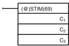
C_1 : Interval timer No. + 3
Interval timer 0: 003
Interval timer 1: 004
Interval timer 2: 005
C_2 : Timer set value (first word address or constant)
C_3 : Subroutine No. (4-digit BCD): 0000 to 0255
| Word | Function |
| C_2 | Decrementing counter set value (4-digit BCD): 0000 to 9999 |
| C_2 + 1 | Decrementing time interval (4-digit BCD; unit: 0.1 ms): 0005 to 0320 (0.5 ms to 32 ms)Note If a constant is used for C_2 , the decrementing time interval is fixed at 0010 or 1 ms, so the set value in C_2 is expressed in ms. |
The meanings of the settings are the same as for the one-shot mode, but in the scheduled interrupt mode the timer PV will be reset to the set value and decrementing will begin again after the subroutine has been called. In the scheduled interrupt mode, interrupts will continue to be repeated at fixed intervals until the operation is stopped.
Reading the Timer's Elapsed Time
Use the STIM(69) instruction to read the timer's elapsed time.
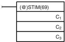
C1: Interval timer No. + 6
Interval timer 0: 006
Interval timer 1: 007
Interval timer 2: 008
C_2 : First word address of parameter 1
| Word | Function |
| C_2 | Number of times the counter has been decremented (4-digit BCD) |
| C_2 + 1 | Decrementing counter time interval (4-digit BCD; unit: 0.1 ms) |
| C_3 | Time elapsed since last decrement (4-digit BCD; unit: 0.1 ms)Note This value will be less than the decrementing counter time interval. |
The time from when the interval timer is started until the execution of this instruction is calculated as follows:
(Contents of word C2) × (Contents of word C2 + 1) + (Contents of word C3) × 0.1 ms
If the specified interval timer is stopped, then "0000" will be stored.
Stopping Timers
Use the STIM(69) instruction to stop the interval timer.
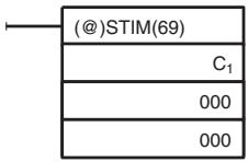
C_1 : Interval timer No. + 10
Interval timer 0: 010
Interval timer 1: 011
Interval timer 2: 012
The specified interval timer will stop.
Application Example
In this example, an interrupt is executed every 2.4 ms (0.6 ms x 4) by means of interval timer 1. Assume the default settings for all of the PC Setup. (Inputs are not refreshed for interrupt processing.)
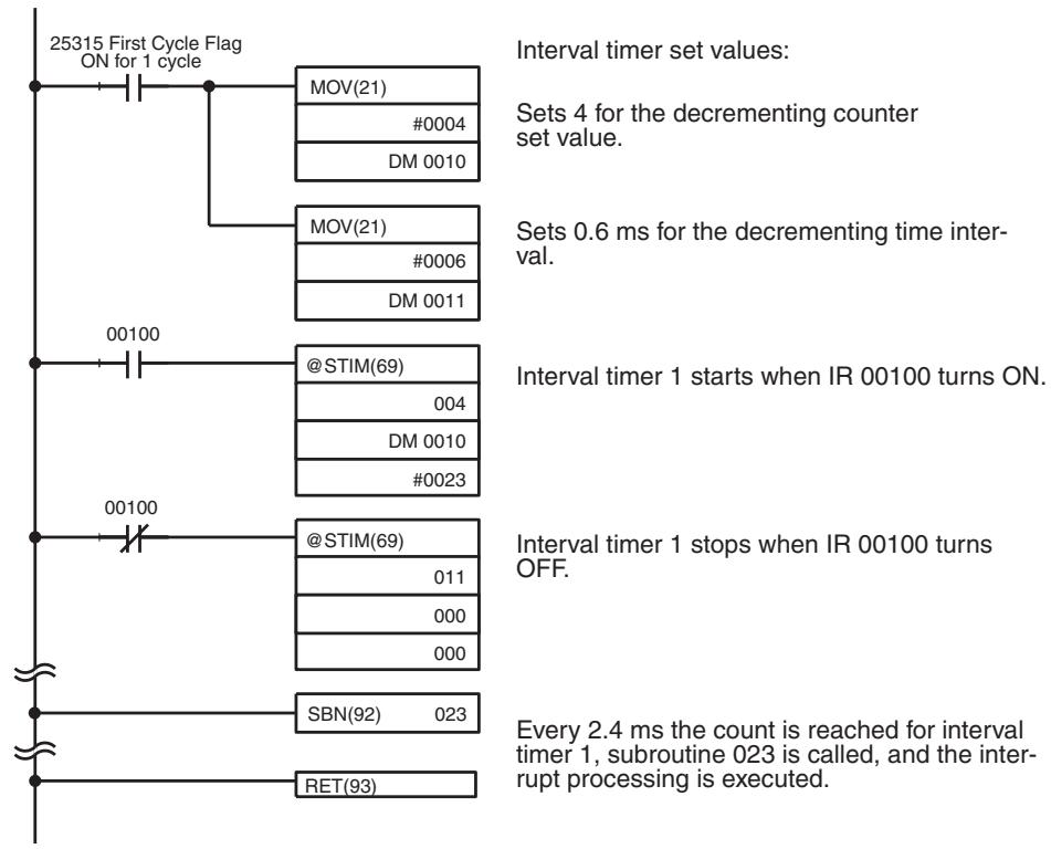
flowchart
graph TD
    A["25315 First Cycle Flag ON for 1 cycle"] --> B["MOV(21)"]
    B --> C["#0004"]
    B --> D["DM 0010"]
    A --> E["MOV(21)"]
    E --> F["#0006"]
    E --> G["DM 0011"]
    A --> H["@STIM(69)"]
    H --> I["004"]
    H --> J["DM 0010"]
    H --> K["#0023"]
    A --> L["@STIM(69)"]
    L --> M["011"]
    L --> N["000"]
    L --> O["000"]
    A --> P["SBN(92)"]
    P --> Q["023"]
    A --> R["RET(93)"]
    R --> S["Every 2.4 ms the count is reached for interval timer 1, subroutine 023 is called, and the interrupt processing is executed"]
When the program is executed, subroutine 023 will be executed every 2.4 ms while IR 00100 is ON.
other
| Event | Duration (ms) | | ------------- | ------------- | | IR 00100 | 2.4 | | Subroutine 023| 2.4 |1-4-6 High-speed Counter 0 Interrupts
Pulse signals from a pulse encoder to CPU bits 00004 through 00006 can be counted at high speed using high-speed counter 0 (the built-in high-speed counter), and interrupt processing can be executed according to the count.
Input Signal Types and Input Modes
Two types of signals can be input from a pulse encoder. The input mode used for high-speed counter 0 will depend on the signal type.
| Mode | Operation |
| Differential phase mode | A phase-difference 4X two-phase signal (phase-A and phase-B) and a phase-Z signal are used for inputs. The count is incremented or decremented according to differences in the 2-phase signals. |
| Incrementing mode | One single-phase pulse signal and a count reset signal are used for inputs. The count is incremented according to the single-phase signal. |
bar
| Phase | Count | |---------|-------| | Phase-A | 1 | | Phase-A | 2 | | Phase-A | 3 | | Phase-A | 4 | | Phase-A | 5 | | Phase-A | 6 | | Phase-A | 7 | | Phase-A | 8 | | Phase-B | 7 | | Phase-B | 6 | | Phase-B | 5 | | Phase-B | 4 | | Phase-B | 3 | | Phase-B | 2 | | Phase-B | 1 | | Phase-B | 0 | | Phase-B | -1 | | Phase-B | -2 |
bar
| Pulse input | Count | | ----------- | ----- | | 1 | 1 | | 2 | 2 | | 3 | 3 | | 4 | 4 |Note One of the methods in the following section should always be used to reset the counter when restarting it. The counter will be automatically reset when program execution is started or stopped.
The following signal transitions are handled as forward (incrementing) pulses: phase-A leading edge to phase-B leading edge to phase-A trailing edge to phase-B trailing edge. The following signal transitions are handled as reverse (decrementing) pulses: phase-B leading edge to phase-A leading edge to phase-B trailing edge to phase-A trailing edge.
The count range is from -32,767 to 32,767 for differential phase mode, and from 0 to 65,535 for Incrementing Mode. Pulse signals can be counted at up to 2.5 kHz in differential phase mode, and up to 5.0 kHz in incrementing mode.
The differential phase mode always uses a 4X phase-difference input. The number of counts for each encoder revolution would be 4 times the resolution of the counter. Select the encoder based on the countable ranges.
Reset Methods
Either of the two methods described below may be selected for resetting the PV of the count (i.e., setting it to 0).
| Method | Operation |
| Phase-Z signal + software reset | The PV is reset when the phase-Z signal (reset input) turns ON after the High-speed Counter 0 Reset Bit (SR 25200) is turned ON. |
| Software reset | The PV is reset when the High-speed Counter 0 Reset Bit (SR 25200) is turned ON. |
other
| Phase-Z (reset input) | Reset by interrupt. | Reset by cycle. | Not reset. | | --------------------- | ------------------- | --------------- | ---------- | | SR25200 | 1 or more cycles | Within 1 cycle | Not reset. |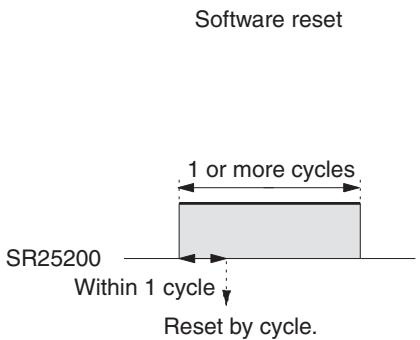
Note The High-speed Counter 0 Reset Bit (SR 25200) is refreshed once every cycle, so in order for it to be read reliably it must be ON for at least one cycle.
The “Z” in “phase-Z” is an abbreviation for “Zero.” It is a signal that shows that the encoder has completed one cycle.
High-speed Counter 0 Interrupt Count
For high-speed counter 0 interrupts, a comparison table is used instead of a "count up." The count check can be carried out by either of the two methods described below. In the comparison table, comparison conditions (for comparing to the PV) and interrupt subroutine combinations are saved.
| Method | Operation |
| Target value | A maximum of 16 comparison conditions (target values and count directions) and interrupt subroutine combinations are saved in the comparison table. When the counter PV and the count direction match the comparison conditions, then the specified interrupt routine is executed. |
| Range comparison | Eight comparison conditions (upper and lower limits) and interrupt routine combinations are saved in the comparison table. When the PV is greater than or equal to the lower limit and less than or equal to the upper limit, then the specified interrupt subroutine is executed. |
Target Value Comparisons
The current count is compared to the target values in the order that target values are set in the comparison table and interrupts are generated as the count equals each target value. Once the count has equaled all of the target values in the table, the target value is set to the first target value in the table, which is again compared to the current counted until the two values are equal.
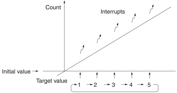
line
| Initial value | Target value | Count | | ------------- | ------------ | ----- | | 1 | 2 | ↑ | | 2 | 3 | ↑ | | 3 | 4 | ↑ | | 4 | 5 | ↑ |Comparison Table
| Target value 1 |
| Target value 2 |
| Target value 3 |
| Target value 4 |
| Target value 5 |
Range Comparisons
The current count is compared in cyclic fashion to all of the ranges at the same time and interrupts are generated based on the results of the comparisons.
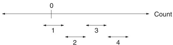
Comparison Table
| Rage setting 1 |
| Rage setting 2 |
| Rage setting 3 |
| Rage setting 4 |
Note When performing target value comparisons, do not repeatedly use the INI instruction to change the current value of the count and start the comparison operation. The interrupt operation may not work correctly if the comparison operation is started immediately after changing the current value from the program. (The comparison operation will automatically return to the first target value once an interrupt has been generated for the last target value. Repetitious operation is thus possible merely by changing the current value.)
Procedure
Follow the steps outlined below when using high-speed counter 0 (the CPU Unit's built-in high-speed counter.)
1,2,3...
- Determine the input mode (differential phase mode or incrementing mode) and reset method (phase-Z signal + software reset, or software reset) to be used.
- Determine the interrupt specifications.
a) No interrupt (Read high-speed counter PV or range comparison results.)
b) Use target-value interrupts or range-comparison interrupts.
- Wire the inputs. (Refer to the CQM1H Operation Manual for details.)
| Terminal | Corresponding bit address | |
| B2 | IN4 | IR 00004 |
| A2 | IN5 | IR 00005 |
| B3 | IN6 | IR 00006 |
- Make PC Setup settings in DM 6642. (See page 39 for more details.)
a) Set 01 in the leftmost byte to indicate that high-speed counter 0 will be used.
b) Set the input mode (differential phase mode or incrementing mode.)
c) Set the reset method (phase-Z signal + software reset, or software reset.)
Note High-speed counter 0 cannot be used while interval timer 2 is being used. (The setting in the leftmost byte of DM 6642 determines whether high-speed counter 0 or interval timer 2 can be used.)
- Program the associated program sections.
a) Use CTBL(63) to register the comparison table and start comparison.
b) Use INI(61) to change the high-speed counter PV or start comparison.
c) Use PRV(62) to read the high-speed counter PV, comparison status, or comparison results.
d) Write an interrupt subroutine within SBN(92) and RET(93) (only when using the high-speed counter 0 interrupt.)
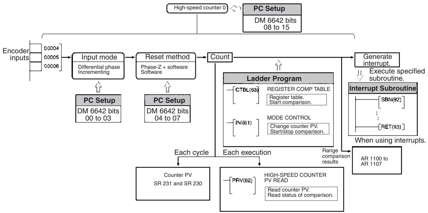
flowchart
graph TD
    A["High-speed counter 0"] --> B["PC Setup"]
    B --> C["DM 6642 bits 08 to 15"]
    C --> D["Input mode"]
    D --> E["Differential phase Incrementing"]
    E --> F["Reset method"]
    F --> G["Phase-Z + software Software"]
    G --> H["Count"]
    H --> I["Ladder Program"]
    I --> J["CTBL(63)"]
    I --> K["REGISTER COMP TABLE"]
    I --> L["Register table. Start comparison."]
    I --> M["INI(61)"]
    I --> N["MODE CONTROL"]
    I --> O["Change counter PV. Start/stop comparison."]
    I --> P["PRV(62)"]
    I --> Q["HIGH-SPEED COUNTER PV READ"]
    I --> R["Read counter PV. Read status of comparison."]
    I --> S["All"]
    T["Generate interrupt."] --> U["Interrupt Subroutine"]
    U --> V["SBN(92)"]
    U --> W["RET(93)"]
    U --> X["When using interrupts."]
    Y["Encoder inputs"] --> Z["00004 00005 00006"]
    Z --> D
    Y --> AA["PC Setup DM 6642 bits 00 to 03"]
    AA --> E
    Y --> AB["PC Setup DM 6642 bits 04 to 07"]
    AB --> F
    Y --> AC["Each cycle Counter PV SR 231 and SR 230"]
    AC --> AD["Each execution PRV(62)"]
    AD --> AE["Range comparison results"]
    AE --> AF["AR 1100 to AR 1107"]
The following instructions are used to control high-speed counter operation.
| Instruction | Control function |
| CTBL(63) | Register a target value comparison table and start comparison. |
| Register a range comparison table and start comparison. | |
| Register a target value comparison table.(Start comparison with INI(61).) | |
| Register a range comparison table.(Start comparison with INI(61).) | |
| INI(61) | Start comparison with registered comparison table. |
| Stop comparison. | |
| Change high-speed counter PV. | |
| PRV(62) | Read high-speed counter PV. |
The following flags and control bits are used to monitor and control high-speed counter operation.
| Word | Bits | Name | Function |
| SR 230 | 00 to 15 | High-speed Counter 0 PV (rightmost 4 digits) | Contains the present value of high-speed counter 0 (the CPU Unit's built-in high-speed counter.) |
| SR 231 | 00 to 15 | High-speed Counter 0 PV (leftmost 4 digits) | |
| SR 252 | 00 | High-speed Counter 0 Reset Bit | Resets the PV of high-speed counter 0. |
| AR 11 | 00 to 07 | High-speed Counter 0 Range Comparison Flags | Indicate the range comparison results for high-speed counter 0.0: Range condition not satisfied.1: Range condition satisfied. |
Wiring
Depending on the input mode, the input signals from the pulse encoder to the CPU Unit's input terminal are as shown below.
| Terminal | Allocated bit address | Differential phase mode | Incrementing mode |
| B2 (IN4) | 00004 | Encoder phase-A | Pulse count input |
| A2 (IN5) | 00005 | Encoder phase-B | --- |
| B3 (IN6) | 00006 | Encoder phase-Z | Reset input |
Note
If the software reset is to be used, IR 00006 can be used as an ordinary input.
- When the input mode is set to incrementing mode, IR 00005 can be used as an ordinary input.
- When the reset method is set to software reset, IR 00006 can be used as an ordinary input.
The following diagram shows a wiring example with an E6B2-CWZ6C NPN open-collector output.
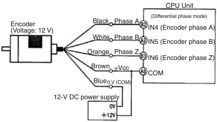
flowchart
graph TD
    A["Encoder (Voltage: 12 V)"] --> B["12-V DC power supply"]
    B --> C["0V +12V"]
    B --> D["Blue₀V (COM)"]
    B --> E["Brown +Vcc"]
    B --> F["Orange Phase Z"]
    B --> G["White Phase B"]
    B --> H["Black Phase A"]
    B --> I["A2 IN5 (Encoder phase B)"]
    B --> J["A3 IN6 (Encoder phase Z)"]
    B --> K["CPU Unit (Differential phase mode)"]
    K --> L["B2 IN4 (Encoder phase A)"]
    K --> M["A8 COM"]
PC Setup
When using high-speed counter 0 interrupts, make the settings in PROGRAM mode shown below before executing the program.
Input Refresh Word Settings (DM 6638)
Make these settings when it is necessary to refresh inputs. The setting is the same as that for interval timer 2.
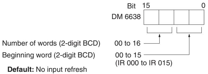
High-speed Counter 0 Settings (DM 6642)
If these settings are not made, high-speed counter 0 cannot be used in the program.
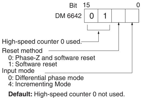
Changes in the setting in DM 6642 become effective only when power is turned ON or PC program execution is started.
Programming
Use the following steps to program high-speed counter 0.
High-speed counter 0 begins the counting operation when the proper PC Setup settings are made, but comparisons will not be made with the compari-
son table and interrupts will not be generated unless the CTBL(63) instruction is executed.
High-speed counter 0 is reset to "0" when power is turned ON and when operation begins.
The present value of high-speed counter 0 is maintained in SR 230 and SR 231.
Controlling High-speed Counter 0 Interrupts
1,2,3... 1. Use the CTBL(63) instruction to save the comparison table in the CQM1H and begin comparisons.
C: (3-digit BCD)
000: Target table set and comparison begun
001: Range table set and comparison begun
002: Target table set only
003: Range table set only
TB: Beginning word of comparison table
If C is set to 000, then comparisons will be made by the target matching method; if 001, then they will be made by the range comparison method. The comparison table will be saved, and, when the save operation is complete, then comparisons will begin. While comparisons are being executed, high-speed interrupts will be executed according to the comparison table. For details on the contents of the comparison tables that are saved, refer to the explanation of the CTBL(63) instruction in SECTION 5 Instruction Set.
Note The comparison results are normally stored in AR 1100 through AR 1107 while the range comparison is being executed.
If C is set to 002, then comparisons will be made by the target matching method; if 003, then they will be made by the range comparison method. For either of these settings, the comparison table will be saved, but comparisons will not begin, and the INI(61) instruction must be used to begin comparisons.
- To stop comparisons, execute the INI(61) instruction as shown below.
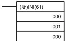
To start comparisons again, set the second operand to "000" (execute comparison), and execute the INI(61) instruction.
Once a table has been saved, it will be retained in the CQM1H during operation (i.e., during program execution) as long as no other table is saved.
Reading the PV
There are two ways to read the PV. The first is to read it from SR 230 and SR 231, and the second to use the PRV(62) instruction.
1,2,3... 1. Reading SR 230 and SR 231
The PV of high-speed counter 0 is stored in SR 230 and SR 231 as shown below. The leftmost digit will be F for negative values.
Leftmost 4 digits
Rightmost 4 digits
Differential phase mode
Incrementing mode
SR 231
SR 230
F0032768 to 00032767 (-32,768)
00000000 to 00065535
Note These words are refreshed only once every cycle, so there may be a difference from the actual PV.
When high-speed counter 0 is not being used, the bits in these words can be used as work bits.
- Using the PRV(62) Instruction
Read the PV of high-speed counter 0 by using the PRV(62) instruction.
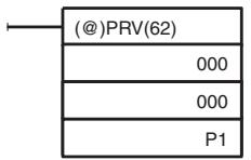
P1: First word address of PV
The PV of high-speed counter 0 is stored as shown below. The leftmost digit will be F for negative values.
Leftmost 4 digits
Rightmost 4 digits
Differential phase mode
Incrementing mode
P1+1
P1
F0032768 to 00032767 (-32,768)
00000000 to 00065535
The PV is read when the PRV(62) instruction is actually executed.
Changing the PV
There are two ways to change the PV of high-speed counter 0. The first way is to reset it by using the reset methods. (In this case the PV is reset to 0.) The second way is to use the INI(61) instruction.
The method using the INI(61) instruction is explained here. For an explanation of the reset method, refer to the beginning of this description of high-speed counter 0.
Change the timer PV by using the INI(61) instruction as shown below.
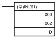
D: First word address for storing PV change data
Leftmost 4 digits
Rightmost 4 digits
Differential phase mode
Incrementing mode
D+1
D
F0032768 to 00032767
00000000 to 00065535
To specify a negative number, set F in the leftmost digit.
Operation Example
This example shows a program for using high-speed counter 0 in the Incrementing Mode, making comparisons by means of the target matching method, and changing the frequency of pulse outputs according to the counter's PV. Before executing the program, set the PC Setup as follows:
DM 6642: 0114 (High-speed counter 0 used with software reset and Incrementing Mode). For all other PC Setup, use the default settings. (Inputs are not refreshed at the time of interrupt processing, and pulse outputs are executed for IR 100.)
In addition, the following data is stored for the comparison table:
DM 0000: 0002 — Number of comparison conditions: 2
DM 0001: 1000 — Target value 1: 1000
DM 0002: 0000
DM 0003: 0101 — Comparison 1 interrupt subroutine: 101
DM 0004: 2000 — Target value 1: 2000
DM 0005: 0000
DM 0006: 0102 — Comparison 2 interrupt subroutine: 102
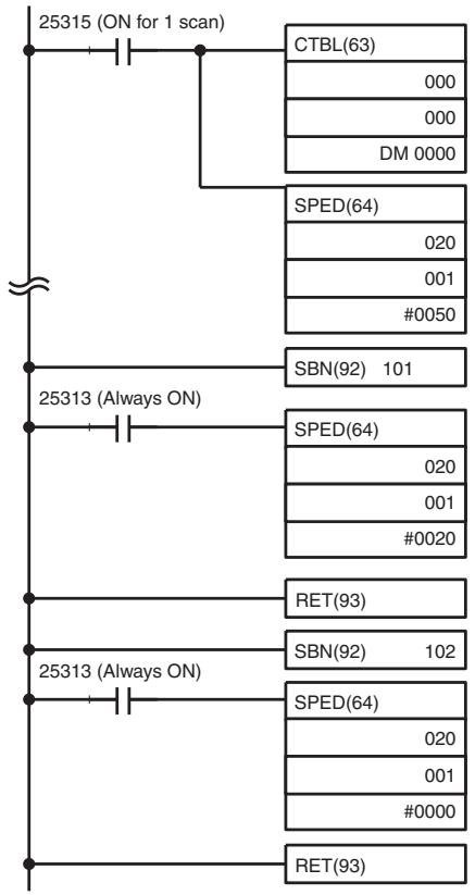
flowchart
graph TD
    A["25315 (ON for 1 scan)"] --> B["CTBL(63)"]
    B --> C["000"]
    B --> D["000"]
    B --> E["DM 0000"]
    A --> F["SPED(64)"]
    F --> G["020"]
    F --> H["001"]
    F --> I["#0050"]
    A --> J["SBN(92) 101"]
    K["25313 (Always ON)"] --> L["SPED(64)"]
    L --> M["020"]
    L --> N["001"]
    L --> O["#0020"]
    K --> P["RET(93)"]
    Q["25313 (Always ON)"] --> R["SPED(64)"]
    R --> S["020"]
    R --> T["001"]
    R --> U["#0000"]
    Q --> V["RET(93)"]
Saves the comparison table in target matching format, and begins comparing.
Begins continuous pulse output to IR10002 at 500 Hz.
When the high-speed counter value reaches 1000, subroutine 101 is called and the frequency of the pulse output is changed to 200 Hz.
When the high-speed counter value reaches 2000, subroutine 102 is called and the pulse output is stopped by setting the frequency to 0.
When the program is executed, operation will be as follows:
line
| Time elapsed (s) | Pulse frequency (Hz) | | ---------------- | -------------------- | | 0 | 500 | | ~100 | 200 | | >100 | 200 | | End | 0 |1-4-7 High-speed Counter 0 Overflows/Underflows
If the allowable counting range for high-speed counter 0 is exceeded, and underflow or overflow status will occur and the counter's PV will remain at 0FFF FFFF for overflows and FFFF FFFF for underflows until the overflow/underflow status is cleared by resetting the counter. The allowable counting ranges are as follows:
Differential phase mode: F003 2768 to 0003 2767
Incrementing Mode: 0000 0000 to 0006 5535
Note
-
The values given above are theoretical and assume a reasonably short cycle time. The values will actually be those that existed one cycle before the overflow/underflow existed.
-
The 6th and 7th digits of high-speed counter 0's PV are normally 00, but can be used as "Overflow/Underflow Flags" by detecting values beyond the allowable counting ranges.
High-speed counter 0 can be reset as described in the previous section or it can be reset automatically by restarting program execution. High-speed counter 0 and related operations will not function normally until the overflow/underflow status is cleared. Operations during overflow/underflow status will be as follows.
- Comparison table operation will stop.
- The comparison table will not be cleared.
- Interrupt routines for the high-speed counter will not be executed.
- CTBL(63) can be used only to register the comparison table. If an attempt is made to start comparison table operation, operation will not start and the comparison table will not be registered.
- INI(61) cannot be used to start or stop comparison table operation or to change the present value.
- PRV(62) will read out only 0FFF FFFF or FFFF FFFF as the present value.
Recovery
Use the following procedure to recover from overflow/underflow status.
With Comparison Table Registered
1,2,3...
- Reset the counter.
- Set the PV with PRV(62) if necessary.
- Set the comparison table with CTBL(63) if necessary
- Start comparison table operation with INI(61).
Without Comparison Table Registered
1,2,3...
- Reset the counter.
- Set the PV with PRV(62) if necessary.
- Set the comparison table and start operation with CTBL(63) and INI(61).
Note
The range comparison results in AR 11 will remain after recovery. The interrupt routine for a interrupt condition meet immediately after recovery will not be executed if the interrupt condition was already met before the overflow/underflow status occurred. If interrupt routine execution is necessary, clear AR 11 before proceeding.
Reset Operation
When high-speed counter 0 is reset, the PV will be set to 0, counting will begin from 0, and the comparison table, execution status, and execution results will be maintained.
Startup Counter Status
When high-speed counter 0 is started, the counter mode in the PC Setup will be read and used, the PV will be set to 0, overflow/underflow status will be cleared, the comparison table registration and execution status will be cleared, and range execution results will be cleared. (Range execution results are always cleared when operation is begun or when the comparison table is registered.)
Stopped Counter Status
When high-speed counter 0 is stopped, the PV will be maintained, the comparison table registration and execution status will be cleared, and range execution results will be maintained.
1-5 Pulse Output Function
This section explains the settings and methods for using the CQM1H pulse output function. Refer to the CQM1H Operation Manual for details on hardware connections to output points and ports.
Standard pulses can be output from a Transistor Output Unit's output using SPED(64). Pulses can be output from just one bit at a time. The duty factor of the pulse output is 50% and the frequency can be set from 20 Hz to 1 kHz.
| Item | Specification |
| Applicable Unit | Transistor Output Unit |
| Pulse output | Pulse output from specified bitAny output word from IR 100 to IR 115 can be specified, but pulses can be output from just one bit of the word at a time. |
| Features | Frequency: 20 Hz to 1 kHzDuty factor: 50%Word specification: PC Setup (DM 6615)Bit specification: In the ladder instruction |
| Applicable instructions | Setting number of pulses: PULS(65)Starting the pulse output: SPED(64)Changing the frequency: SPED(64)Stopping the pulse output: SPED(64) or INI(61) |
Pulse Output Operations
The following table shows the pulse output operations that can be made with combinations of PULS(65), SPED(64), and INI(61).
Note A Transistor Output Unit must be used for this application.
| Frequency change | Instruction | Operand settings | |
 | Start pulse output at the specified frequency. Outputs continuously (continuous mode) or until the specified number of pulses have been output (independent mode.) (Execute PULS(65) and then SPED(64) when using independent mode.) | PULS(65) | Number of pulses (independent mode only) |
| SPED(64) | Port Mode Frequency | ||
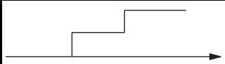 | Change the frequency (in steps) of pulses being output. | SPED(64) | Port Mode Frequency |
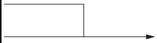 | Stop pulse output with an instruction. (Execute SPED(64) or INI(61).) | SPED(64) | Port Frequency= 0 |
| INI(61) (See note.) | Control word=003 | ||
Note Stop pulse outputs only when pulses are actually being output. The current output status can be read from the Pulse Output In Progress Flag (AR 0515 or AR 0615).
When outputting pulses from an output point, the frequency can be changed in steps by executing SPED(64) again with different frequencies, as shown in the following diagram.
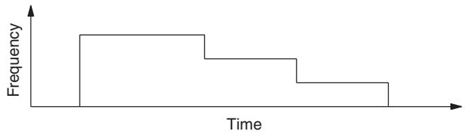
line
| Time | Frequency | | ---- | --------- | | 0 | 100 | | 1 | 100 | | 2 | 50 | | 3 | 50 | | 4 | 25 | | 5 | 25 |Pulses can be output from an output in continuous mode or independent mode.
Continuous Mode
Pulses are output continuously until stopped with SPED(64) or INI(61).
Independent Mode
The pulse output stops automatically once the number of pulses specified in SPED(64) have been output. (The pulse output can also be stopped prematurely with SPED(64) or INI(61).)
Procedure
Follow the steps outlined below when outputting pulses from a Transistor Output Unit. Pulses can be output from only one terminal on the Transistor Output Unit at a time.
1,2,3...
- Determine the IR word (IR 100 to IR 115) to be used for the pulse output.
- Wire the Transistor Output Unit. Wire the terminal corresponding to the bit that will actually be used in the selected word.
- Set the desired IR word address in DM 6615 of the PC Setup. Settings 0000 to 0015 BCD correspond to IR 100 to IR 115. (See page 46 for more details.)
- Program the associated program sections.
a) PULS(65) can be used to set the number of output pulses.
b) SPED(64) can be used to control the pulse output (a pulse output without acceleration or deceleration.)
c) INI(61) can be used to stop the pulse output.
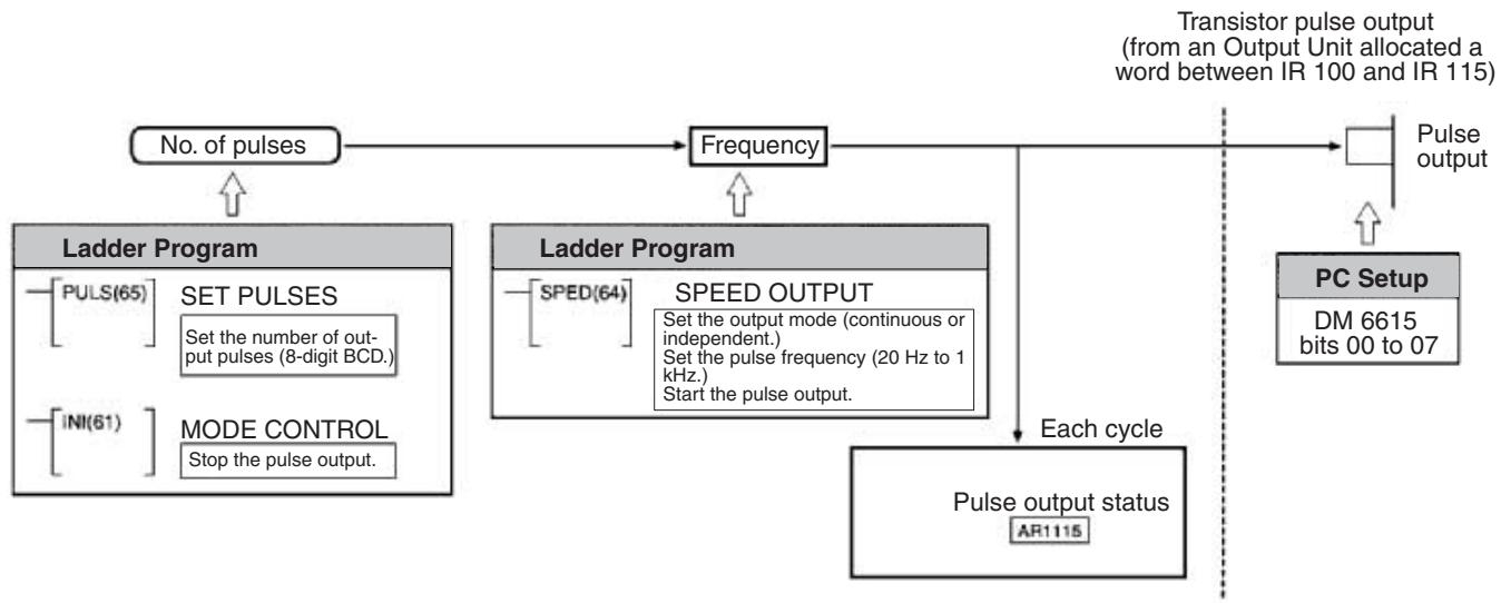
flowchart
graph TD
    A["No. of pulses"] --> B["Frequency"]
    B --> C["Pulse output"]
    C --> D["PC Setup DM 6615 bits 00 to 07"]
    D --> E["Pulse output status AR1115"]
    E --> F["Each cycle"]
    F --> G["Ladder Program"]
    G --> H["Ladder Program"]
    H --> I["Mode CONTROL Stop the pulse output."]
    G --> J["SET PULSES Set the number of output pulses (8-digit BCD.)"]
    G --> K["INI(61)"]
    H --> L["SPEED(64)"]
    L --> M["SPEED OUTPUT Set the output mode (continuous or independent.) Set the pulse frequency (20 Hz to 1 kHz.) Start the pulse output."]
    style A fill:#f9f,stroke:#333
    style B fill:#ccf,stroke:#333
    style C fill:#cfc,stroke:#333
    style D fill:#fcc,stroke:#333
    style E fill:#cff,stroke:#333
PC Setup Settings
Before executing SPED(64) to output pulses from an Output Unit, set the PC to PROGRAM mode and make the following settings in the PC Setup.
In DM 6615, specify the output word that will be used for SPED(64) pulse output to Output Units. (The bit is specified in the first operand in SPED(64).)
The content of DM 6615 (0000 to 0015) specifies output words IR 100 to IR 115. For example, if DM 6615 is set to 0002, pulses will be output to IR 102.
Default: Pulse output to IR 100.
Continuous Pulse Output
Pulses will begin to be output at the specified output bit when SPED(64) is executed. Set the output bit from 00 to 15 (D=000 to 150) and the frequency from 20 Hz to 1000 Hz (F=0002 to 0100). Set the mode to continuous mode (M=001).
flowchart
graph LR
    A["Execution condition"] --> B["@SPED(64)"]
    B --> C["D"]
    B --> D["M"]
    B --> E["F"]
The pulse output can be stopped by executing INI(61) with C=003 or executing SPED(64) again with the frequency set to 0. The frequency can be changed by executing SPED(64) again with a different frequency setting.
Setting the Number of Pulses
The total number of pulses that will be output can be set with PULS(65) before executing SPED(64) in independent mode. The pulse output will stop automatically when the number of pulses set by PULS(65) have been output.
flowchart
graph TD
    A["Execution condition"] --> B["@PULS(65)"]
    B --> C["000"]
    B --> D["000"]
    B --> E["P1"]
PULS(65) sets the 8-digit number of pulses P1+1, P1. These pulses can be set from 00000001 to 16777215. The number of pulses set with PULS(65) is accessed when SPED(64) is executed in independent mode. (The number of pulses cannot be changed for pulses that are being output.)
flowchart
graph LR
    A["Execution condition"] --> B["@SPED(64)"]
    B --> C["D"]
    B --> D["M"]
    B --> E["F"]
When SPED(64) is executed, pulses will begin to be output at the specified output bit (D=000 to 150: bit 00 to 15) at the specified frequency (F=0002 to 0100: 20 Hz to 1000 Hz). Set the mode to independent mode (M=000) to output the number of pulses set with PULS(65). The frequency can be changed by executing SPED(64) again with a different frequency setting.
Changing the Frequency
The frequency of the pulse output can be changed by executing SPED(64) again with a different frequency setting. Use the same output bit (P) and mode (M) settings that were used to start the pulse output. The new frequency can be frequency 20 Hz to 1000 Hz (F=0002 to 0100).
1-6 Communications Functions
The following table shows which communications modes are supported by the CQM1H CPU Unit's communications ports. (The CQM1H-CPU11 CPU Unit is not equipped with an RS-232C port.)
The PC Setup settings and communications procedures for these communications modes are described later in this section.
| Communications | Uses | Port | |
| Peripheral | RS-232C | ||
| Programming Console bus | Programming Console connection | YES | No |
| Peripheral bus | Connection to a personal computer with Support Software | YES | No |
| Host Link | Host Link or Programmable Terminal connection | YES | YES |
| Protocol Macro | Data transfer with standard external devices using arbitrary protocol | No | No |
| No-protocol | No-protocol communications with standard external devices | YES | YES |
| 1:1 data link | Establishing a data link with another CPU Unit | No | YES |
| NT Link in 1:1 mode | Establishing a 1:1 Data Link with a Programmable Terminal | No | YES(See note.) |
| NT Link in 1:N mode | Establishing a 1:1 Data Link with a Programmable Terminal or a 1:N connection with two or more Programmable Terminals | No | No |
Note
- The Programmable Terminal's Programming Console functions can be used, but pin 7 on the DIP switch must be ON.
- Turn ON pin 7 of the CPU Unit's DIP Switch when using the peripheral port for any device other than a Programming Console.
Automatic Mode Change
When the PC is in RUN mode with a Programming Console connected to the peripheral port of the CPU Unit, if a PT is connected to the CPU Unit's built-in RS-232C port or either of the ports of a CQM1H-SCB41 using Host Link mode, the following message will be displayed at the Programming Console indicating that a password is required to continue operation (using the Programming Console).
This is because, in order to write data to the CPU Unit, the PT changed the operation mode from RUN mode to MONITOR mode. To continue operation using the Programming Console, it is necessary to input the password again.
Inputting the Password
- The mode will not be changed if the PT is connected via an NT Link.
- When a Programming Device installed on a computer is connected to the peripheral port, the display (at the computer) for the CPU Unit's operation mode will simply change from "RUN" to "MONITOR."
1-6-1 Host Link and No-protocol Communications Settings
This section explains the PC Setup settings that are shared by the Host Link and no-protocol communications modes. Make the required PC Setup settings before attempting to establish Host Link or no-protocol communications.
Note If pin 5 on the CQM1H's DIP switch is turned ON, the PC Setup communications parameters will be ignored and the following settings will be used.
| Parameter | Setting when DIP Switch pin 5 is ON |
| Communications mode | Host Link |
| Node number | 00 |
| Start bits | 1 bit |
| Data length | 7 bits |
| Stop bits | 2 bit |
| Parity | Even |
| Baud rate | 9,600 bps |
| Transmission delay | None |
The PC Setup parameters in DM 6645 through DM 6654 are used to set parameters for the communications ports.
Communications Settings (DM 6645 and DM 6650)
The settings in DM 6645 and DM 6650 determine the main communications parameters, as shown in the following diagram.
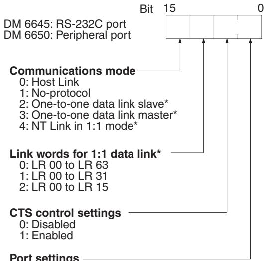
0: Standard communication conditions 1: According to setting in DM 6646, DM 6651
Default (0000): Host Link using standard parameters, no CTS control
Note *These settings can be made for the RS-232C port (DM 6645), but not for the peripheral port (DM 6650).
Communications Settings (DM 6646 and DM 6651)
When pin 5 of the CPU Unit's DIP Switch is OFF and the settings in DM 6646 (or DM 6651) are enabled in DM 6645 (or DM 6650), these settings determine the transmission frame format and baud rate, as shown in the following diagram.
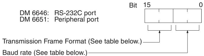
Default: Standard communication conditions.
Transmission Frame Format
| Setting | Stop bits | Data length | Stop bits | Parity |
| 00 | 1 | 7 | 1 | Even |
| 01 | 1 | 7 | 1 | Odd |
| 02 | 1 | 7 | 1 | None |
| 03 | 1 | 7 | 2 | Even |
| 04 | 1 | 7 | 2 | Odd |
| 05 | 1 | 7 | 2 | None |
| 06 | 1 | 8 | 1 | Even |
| 07 | 1 | 8 | 1 | Odd |
| 08 | 1 | 8 | 1 | None |
| 09 | 1 | 8 | 2 | Even |
| 10 | 1 | 8 | 2 | Odd |
| 11 | 1 | 8 | 2 | None |
Baud Rate
| Setting | Baud rate |
| 00 | 1,200 bps |
| 01 | 2,400 bps |
| 02 | 4,800 bps |
| 03 | 9,600 bps |
| 04 | 19,200 bps |
Transmission Delay Time (DM 6647 and DM 6652)
Depending on the devices connected to the communications port, it may be necessary to allow time for transmission. When that is the case, set the transmission delay to regulate the amount of time allowed.
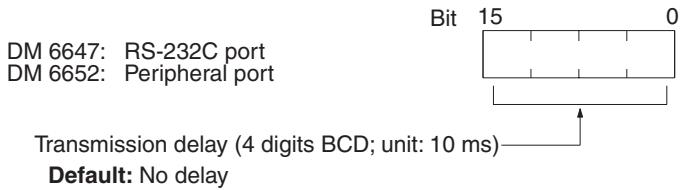
The transmission delay is set in the PC Setup to create a minimum interval between sending data from the PC. The transmission delay is used for the following serial communications modes.
| Serial communications mode | Application |
| Host Link, responses | Once the PC has sent a response to the host computer, it will not send the next response until the time set for the transmission delay has expired. |
| Host Link, PC-initiated communications | Once the PC has sent data using TXD(48), it will not send data again until the time set for the transmission delay has expired. |
| No-protocol communications |
The delay is not used the first time data is sent from the PC. The delay will affect other sends only if the normal time for the send comes before the time set for the transmission delay has expired.
If the delay time has already expired when the next send is ready, the data will be spent immediately. If the delay time has not expired, the send will be delayed until the time set for the transmission delay has expired.
The operation of the transmission delay for data sent from the PC is illustrated below.
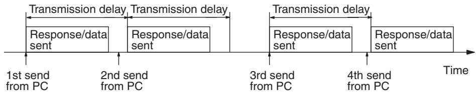
1-6-2 Host Link Communications Settings and Procedures
This section explains the PC Setup settings and procedure required for Host Link communications.
PC Setup Settings
Be sure to write 00 in the leftmost digits of DM 6645 (RS-232C port) or DM 6650 (peripheral port) to specify Host Link communications. Other Host Link communications parameters are set in the rightmost two digits of DM 6645/DM 6650 and DM 6646/DM 6651.
A node number must be set for Host Link communications to differentiate between nodes when multiple nodes are participating in communications. This setting is required only for Host Link communications.
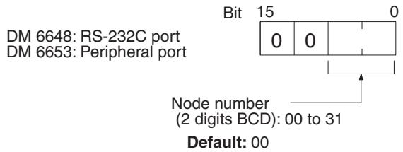
The node number is normally set to 00. Other settings are not required unless multiple nodes are connected in a network.
Overview of Host Link Communications
Host Link communications were developed by OMRON for the purpose of connecting PCs and one or more host computers by RS-232C cable, and controlling PC communications from the host computer. Normally the host computer issues a command to a PC, and the PC automatically sends back a response. Thus the communications are carried out without the PCs being actively involved. The PCs also have the ability to initiate data transmissions when direct involvement is necessary.
In general, there are two means for implementing Host Link communications. One is based on C-mode commands, and the other on FINS (CV-mode) commands. The CQM1H supports C-mode commands only. For details on Host Link communications, refer to SECTION 6 Host Link Commands.
Communications Procedure
This section explains how to use the Host Link to execute data transmissions from the CQM1H. Using this method enables automatic data transmission from the CQM1H when data is changed, and thus simplifies the communications process by eliminating the need for constant monitoring by the computer.
1,2,3...
- Check to see that AR 0805 (RS-232C Port Transmission Enabled Flag) is ON.
- Use the TXD(48) instruction to transmit the data.
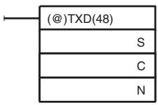
S: Beginning word address of transmission data
C: Control data
0000: RS-232C port
1000: Peripheral port
N: Number of bytes of data to be sent (4 digits BCD)
0000 to 0061
From the time this instruction is executed until the data transmission is complete, AR 0805 (or AR 0813 for the peripheral port) will remain OFF. It will turn ON again upon completion of the data transmission. The TXD(48) instruction does not provide a response, so in order to receive confirmation that the computer has received the data, the computer's program must be written so that it gives notification when data is written from the CQM1H.
The transmission data frame is as shown below for data transmitted in the Host Link Mode by means of the TXD(48) instruction.
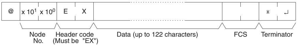
To reset the RS-232C port (i.e., to restore the initial status), turn ON SR 25209. To reset the peripheral port, turn ON SR 25208. These bits will turn OFF automatically after the reset.
If the TXD(48) instruction is executed while the CQM1H is in the middle of responding to a command from the computer, the response transmission will first be completed before the transmission is executed according to the TXD(48) instruction. In all other cases, data transmission based on a TXD(48) instruction will be given first priority.
Application Example
This example shows a program for using the RS-232C port in the Host Link Mode to transmit 10 bytes of data (DM 0000 to DM 0004) to the computer. The default values are assumed for all the PC Setup (i.e., the RS-232C port is used in Host Link Mode, the node number is 00, and the standard communications conditions are used.) From DM 0000 to DM 0004, "1234" is stored in every word. From the computer, execute a program to receive CQM1H data with the standard communications conditions.
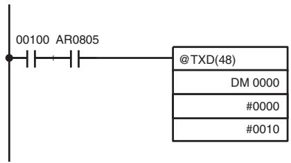
If AR 0805 (the Transmission Enabled Flag) is ON when IR 00100 turns ON, the ten bytes of data (DM 0000 to DM 0004) will be transmitted.
The following type of program must be prepared in the host computer to receive the data. This program allows the computer to read and display the data received from the PC while a Host Link read command is being executed to read data from the PC.
10 'CQM1H SAMPLE PROGRAM FOR EXCEPTION
20 CLOSE 1
30 CLS
40 OPEN "COM:E73" AS #1
50 *KEYIN
60 INPUT "DATA ----",S$
70 IF S$=" " THEN GOTO 190
80 PRINT "SEND DATA = ";S$
90 ST=S
100 INPUT "SEND OK? Y or N?=",B$
110 IF B$="Y" THEN GOTO 130 ELSE GOTO *KEYIN
120 S=ST
130 PRINT #1,S$
140 INPUT #1,R$
150 PRINT "RECV DATA = ";R$
160 IF MID(R,4,2)="EX" THEN GOTO 210 'Identifies command from PC
170 IF RIGHT(R,1)<>"*" THEN S$=" ":GOTO 130
180 GOTO *KEYIN
190 CLOSE 1
200 END
210 PRINT "EXCEPTION!! DATA"
220 GOTO 140
The data received by the computer will be as shown below. (FCS is “59.”) "@00EX1234123412341234123459*CR"
1-6-3 No-protocol Communications Settings and Procedures
This section explains the PC Setup settings and procedure required for No-protocol communications. No-protocol communications allow data to be exchanged with standard devices. For example, data can be output to a printer or input from a bar code reader.
PC Setup Settings
Be sure to write 10 in the leftmost digits of DM 6645 (RS-232C port) or DM 6650 (peripheral port) to specify No-protocol communications. Other communications parameters are set in the rightmost two digits of DM 6645/DM 6650 and DM 6646/DM 6651.
The start and end codes or the amount of data to be received can be set as shown in the following diagrams if required for no-protocol communications. This setting is required only for no-protocol communications. These settings are valid only when pin 5 on the DIP Switch is OFF.
Enabling Start and End Codes
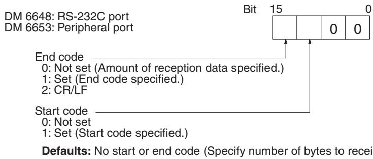
Specify whether or not a start code is to be set at the beginning of the data, and whether or not an end code is to be set at the end. Instead of setting the end code, it is possible to specify the number of bytes to be received before the reception operation is completed. Both the codes and the number of bytes of data to be received are set in DM 6649 or DM 6654.
Setting the Start Code, End Code, and Amount of Reception Data
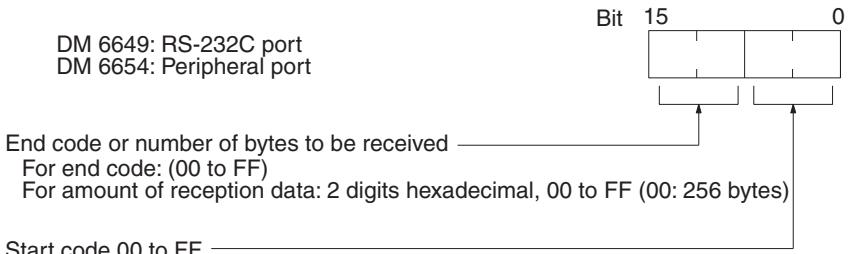
Defaults: No start code; data reception complete at 256 bytes.
Communications Procedure
Transmissions
1,2,3... 1. Check to see that AR 0805 (the RS-232C Port Transmission Enabled Flag) has turned ON.
2. Use the TXD(48) instruction to transmit the data.
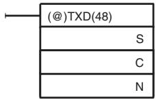
S: Leading word of data to be transmitted
C: Control data
N: Number of bytes to be transmitted (4 digits BCD), 0000 to 0256
From the time this instruction is executed until the data transmission is complete, AR 0805 (or AR0813 for the peripheral port) will remain OFF. (It will turn ON again upon completion of the data transmission.)
Start and end codes are not included when the number of bytes to be transmitted is specified. The largest transmission that can be sent with or without start and end codes in 256 bytes, N will be between 254 and 256 depending on the designations for start and end codes. If the number of bytes to be sent is set to 0000, only the start and end codes will be sent.
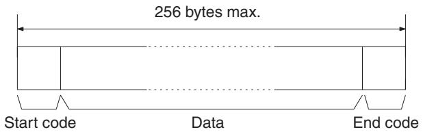
To reset the RS-232C port (i.e., to restore the initial status), turn ON SR 25209. To reset the peripheral port, turn ON SR 25208. These bites will turn OFF automatically after the reset.
Receptions
1,2,3... 1. Confirm that AR 0806 (RS-232C Reception Completed Flag) or AR 0814 (Peripheral Reception Completed Flag) is ON.
2. Use the RXD(47) instruction to receive the data.
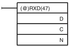
D: Leading word for storing reception data
C: Control data
Bits 00 to 03
0: Leftmost bytes first
1: Rightmost bytes first
Bits 12 to 15
0: RS-232C port
1: Peripheral port
N: Number of bytes stored (4 digits BCD), 0000 to 0256
- The results of reading the data received will be stored in the AR area. Check to see that the operation was successfully completed. The contents of these bits will be reset each time RXD(47) is executed.
| RS-232C port | Peripheral port | Error |
| AR 0800 to AR 0803 | AR 0808 to AR 0811 | RS-232C port error code (1 digit BCD) 0: Normal completion 1: Parity error 2: Framing error 3: Overrun error |
| AR 0804 | AR0812 | Communications error |
| AR 0807 | AR0815 | Reception Overrun Flag (After reception was completed, the subsequent data was received before the data was read by means of the RXD(47) instruction.) |
| AR 09 | AR10 | Number of bytes received (4-digit BCD) |
To reset the RS-232C port (i.e., to restore the initial status), turn ON SR 25209. To reset the peripheral port, turn ON SR 25208. These bits will turn OFF automatically after the reset.
The start code and end code are not included in AR 09 or AR 10 (number of bytes received).
Application Example
This example shows a program for using the RS-232C port in the no-protocol mode to transmit 10 bytes of data (DM 0100 to DM 0104) to the computer, and to store the data received from the computer in the DM area beginning with DM 0200. Before executing the program, the following PC Setup setting must be made.
DM 6645: 1000 (RS-232C port in no-protocol mode; standard communications conditions)
DM 6648: 2000 (No start code; end code CR/LF)
The default values are assumed for all other PC Setup settings. From DM 0100 to DM 0104, 3132 is stored in every word. From the computer, execute a program to receive CQM1H data with the standard communications conditions.
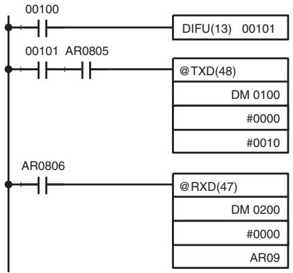
flowchart
graph TD
    A["00100"] --> B["DIFU(13) 00101"]
    C["00101 AR0805"] --> D["@TXD(48)"]
    E["AR0806"] --> F["@RXD(47)"]
    B --> G["DM 0100"]
    D --> H["#0000"]
    F --> I["DM 0200"]
    G --> J["#0000"]
    H --> K["AR09"]
If AR 0805 (the Transmission Enabled Flag) is ON when IR 00100 turns ON, the ten bytes of data (DM 0100 to DM 0104) will be transmitted, leftmost bytes first.
When AR 0806 (Reception Completed Flag) goes ON, the number of bytes of data specified in AR 09 will be read from the CQM1H's reception buffer and stored in memory starting at DM 0200, leftmost bytes first.
The data will be as follows: "31323132313231323132CR LF"
1-6-4 One-to-one Data Links
If a CQM1H is linked one-to-one by connecting it to another CPU Unit through their RS-232C ports, they can share common LR areas. One of the PCs will serve as the master and the other as the slave. A CQM1H can be linked one-to-one with any of the following PCs: CQM1H, CQM1, C200HX/HG/HE, C200HS, CPM1, CPM1A, CPM2A, CPM2C, or SRM1(-V2).
Note The peripheral port cannot be used for 1:1 Data Links. Use the CPU Unit's built-in RS-232C port or a Serial Communications Board's RS-232C or RS-422A/485 port.
One-to-one Data Links
A 1:1 Data Link allows two CQM1Hs to share common data in their LR areas. As shown in the diagram below, when data is written into a word the LR area of one of the linked Units, it will automatically be written identically into the same word of the other Unit. Each PC has specified words to which it can write and specified words that are written to by the other PC. Each can read, but cannot write, the words written by the other PC.
Master area
Slave area
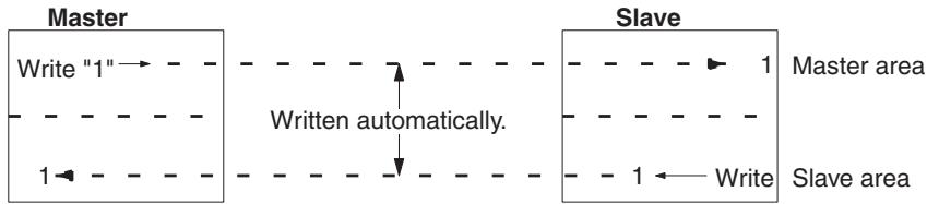
flowchart
graph LR
    subgraph Master
        A["Write "1""] --> B["---"]
        C["1"] --> D["---"]
        E["---"] --> F["---"]
    end
    subgraph Slave
        G["Write 1"] --> H["---"]
        I["1"] <--_J["---"]
        K["---"] --> L["---"]
        M["---"] --> N["---"]
        O["---"] --> P["---"]
        Q["---"] --> R["---"]
        S["---"] --> T["---"]
        U["---"] --> V["---"]
    end
    style Master fill:#f9f,stroke:#333
    style Slave fill:#bbf,stroke:#333
    note right of Master: "Written automatically."
    note left of Slave: Master area
    note right of Slave: Slave area
The word used by each PC will be as shown in the following table, according to the settings for the master, slave, and link words. Set the link area to LR 00 to LR 15 if the CQM1H is being linked with a CPM1, CPM1A, CPM2A, or SRM1(-V2) PC.
| DM 6645 setting | Master area | Slave area |
| LR 00 to LR 15 | LR 00 to LR 07 | LR 08 to LR 15 |
| LR 00 to LR 31 | LR 00 to LR 15 | LR 16 to LR 31 |
| LR 00 to LR 63 | LR 00 to LR 31 | LR 32 to LR 63 |
PC Setup Settings
To use a 1:1 Data Link, the only settings necessary are the communications mode and the link words. Set the communications mode for one of the PCs to the 1:1 Data Link Master and the other to the 1:1 Data Link Slave, and then set the link words in the PC designated as the master.
Default: Communications mode = 0 (Host Link)
Note These settings are valid only when pin 5 of the CPU Unit's DIP Switch is OFF. Bits 08 to 11 are valid only in the 1:1 Data Link Master.
Communications Procedure
If the settings for the master and the slave are made correctly, then the One-to-one Data Link will be automatically started up simply by turning on the power supply to both of the CPU Units and operation will be independent of the CPU Units' operating modes.
Link Errors
If a slave does not receive a response from the master within one second, the 1:1 Data Link Error Flag (AR 0802) and the Communications Error Flag (AR 0804) will be turned ON.
Application Example
This example shows a program for verifying the conditions for executing a One-to-one Data Link using the RS-232C ports. Before executing the program, set the following PC Setup parameters.
Master: DM 6645: 3200 (1:1 Data Link Master; Area used: LR 00 to LR 15)
Slave: DM 6645: 2000 (1:1 Data Link Slave)
The defaults are assumed for all other PC Setup parameters. The words used for the One-to-one Data Link are as shown below.
flowchart
graph LR
    subgraph Master
        A["LR 00"] --> B["Area for writing"]
        C["LR 07"] --> D["Area for reading"]
        E["LR 08"] --> D
        F["LR 15"] --> D
    end

    subgraph Slave
        G["LR 00"] --> H["Area for reading"]
        I["LR 07"] --> J["Area for writing"]
        K["LR 08"] --> J
        L["LR 15"] --> J
    end
When the program is executed at both the master and the slave, the status of IR 001 of each Unit will be reflected in IR 100 of the other Unit. Likewise, the status of the other Unit's IR 001 will be reflected in IR 100 of each Unit. IR 001 is an input word and IR 100 is an output word
In the Master
flowchart
graph TD
    A["25313 (Always ON)"] --> B["MOV(21)"]
    A --> C["MOV(21)"]
    B --> D["001"]
    B --> E["LR00"]
    C --> F["LR08"]
    C --> G["100"]
In the Slave
flowchart
graph TD
    A["25313 (Always ON)"] --> B["MOV(21)"]
    A --> C["MOV(21)"]
    B --> D["001"]
    B --> E["LR08"]
    C --> F["LR00"]
    C --> G["100"]
1-6-5 NT Link 1:1 Mode Communications
This section explains communications with a Programmable Terminal with the communications mode set to NT Link in 1:1 mode. The peripheral port cannot be used for NT Link communications.
Settings
Set the communications mode to NT Link in 1:1 mode by setting DM 6645 to 4000. Be sure that pin 5 of the CPU Unit's DIP Switch is OFF.
For details on Programmable Terminal settings, refer to the Programming Terminal's Operation Manual.
Overview of NT Link 1:1 Mode Communications
NT Link communications were developed by OMRON to provide high-speed communications between the PC and a Programmable Terminal. There are two kinds of NT Link communications: 1:1 mode in which a single Programmable Terminal is connected to the PC and 1:N mode in which several Programmable Terminals can be connected to the PC. The CQM1H's built-in RS-232C port supports only 1:1 mode communications, but both 1:1 and 1:N
modes can be used if an optional Serial Communications Board is installed in the PC.
Some Programmable Terminals are equipped with Programming Console functions which allow the Programmable Terminal to program and monitor the CQM1H. The Programmable Terminal's Programming Console functions cannot be used if a Programming Console is connected to the CQM1H's peripheral port. Refer to the Programming Terminal's Operation Manual for details on the Programming Console functions.
Communications Procedure
With NT Link communications, the PC automatically responds to commands issued from the Programmable Terminal, so communications programming is not required in the CQM1H and there is no NT Link communications procedure to perform.
1-6-6 Wiring Ports
Refer to the CQM1H Operation Manual for information on wiring the communications ports.
1-7 Calculating with Signed Binary Data
The CQM1H PCs allow calculations on signed binary data. The following instructions manipulate signed binary data. Signed data is handled using 2's complements.
The following signed-binary instructions are available in CQM1H PCs:
Single-word Instructions
- 2'S COMPLEMENT – NEG(—)
- BINARY ADD – ADB(50)
• BINARY SUBTRACT – SBB(51)
• SIGNED BINARY MULTIPLY – MBS(—)
• SIGNED BINARY DIVIDE – DBS(—)
Double-word (Long) Instructions
- DOUBLE 2'S COMPLEMENT – NEGL(—)
- DOUBLE BINARY ADD – ADBL(—)
- DOUBLE BINARY SUBTRACT – SBBL(—)
- DOUBLE SIGNED BINARY MULTIPLY – MBSL(—)
- DOUBLE SIGNED BINARY DIVIDE – DBSL(—)
1-7-1 Definition of Signed Binary Data
The CQM1H provides instructions that operate on either one or two words of data. Signed binary data is manipulated using 2's complements and the MSB of the one- or two-word data is used as the sign bit. The range of data that can be expressed using one or two words is thus as follows:
- One-word data:
-32,768 to 32,767 (8000 to 7FFF hexadecimal) - Two-word data:
-2,147,483,648 to 2,147,483,647 (8000 0000 to 7FFF FFFF hexadecimal)
The following table shows equivalents between decimal and hexadecimal data.
| Decimal | 16-bit Hex | 32-bit Hex |
| 2,147,483,647 | — | 7FFF FFFF |
| 2,147,483,646 | — | 7FFF FFFE |
| . | . | . |
| . | . | . |
| . | . | . |
| 32,768 | — | 0000 8000 |
| 32,767 | 7FFF | 0000 7FFF |
| 32,766 | 7FFE | 0000 7FFE |
| . | . | . |
| . | . | . |
| . | . | . |
| 2 | 0002 | 0000 0002 |
| 1 | 0001 | 0000 0001 |
| 0 | 0000 | 0000 0000 |
| -1 | FFFF | FFFF FFFF |
| -2 | FFFE | FFFF FFFE |
| . | . | . |
| . | . | . |
| . | . | . |
| -32,767 | 8001 | FFFF 8001 |
| -32,768 | 8000 | FFFF 8000 |
| -32,769 | — | FFFF 7FFF |
| . | . | . |
| . | . | . |
| . | . | . |
| -2,147,483,647 | — | 8000 0001 |
| -2,147,483,648 | — | 8000 0000 |
1-7-2 Arithmetic Flags
The results of executing signed binary instructions is reflected in the arithmetic flags. The flags and the conditions under which it will turn ON are given in the following table. The flags will be OFF when these conditions are not met.
| Flag | ON conditions |
| Carry Flag (SR 25504) | Carry in an addition.Negative results for subtraction. |
| Equals Flag (SR 25506) | The results of addition, subtraction, multiplication, or division is 0.Results of converting 2's complement is 0. |
| Overflow Flag (SR 25404) | 32,767 (7FFF) was exceeded in results of 16-bit addition or subtraction.2,147,483,647 (7FFF FFFF) was exceeded in results of 32-bit addition or subtraction. |
| Underflow Flag (SR 25405) | -32,768 (8000) was exceeded in results of 16-bit addition or subtraction, or conversion of 2's complement.-2,147,483,648 (8000 0000) was exceeded in results of 32-bit addition or subtraction, or conversion of 2's complement. |
1-7-3 Inputting Signed Binary Data Using Decimal Values
Although calculations for signed binary data use hexadecimal expressions, inputs from the Programming Console or CX-Programmer can be done using decimal inputs and mnemonics for the instructions. The procedure for using the Programming Console to input using decimal values is shown in the
CQM1H Operation Manual. Refer to the CX-Programmer Operation Manual: C-series PCs for details on using the CX-Programmer.
Input Instructions
Only 16-bit operands can be input for the following instructions: NEG(—), ADB(50), SBB(51), MBS(—), and DBS(—). Refer to the CQM1H Operation Manual for details on inputting instructions from the Programming Console.
1-7-4 Using Signed-binary Expansion Instructions
The following CQM1H instructions must be allocated function codes in the instructions table before they can be used.
- 2'S COMPLEMENT – NEG(—)
- DOUBLE 2'S COMPLEMENT – NEGL(—)
- DOUBLE BINARY ADD – ADBL(—)
- DOUBLE BINARY SUBTRACT – SBBL(—)
- SIGNED BINARY MULTIPLY – MBS(—)
- DOUBLE SIGNED BINARY MULTIPLY – MBSL(—)
- SIGNED BINARY DIVIDE – DBS(—)
- DOUBLE SIGNED BINARY DIVIDE – DBSL(—)
Allocating Function Codes
The procedure to using the Programming Console to allocate function codes is shown in the CQM1H Operation Manual. Be sure that pin 4 of the CQM1H's DIP switch is turned ON to enable use of a user-set instruction table before performing this operation.
1-7-5 Application Example Using Signed Binary Data
The following programming can be used to performed calculations such as the following in the CQM1H:
$$ ((1 2 3 4 + (- 1 2 3)) \times 1 2 1 2 - 1 2 3 4 5) \div (- 1 2 3 4) = - 1 0 8 1, \text { Remainder of } 2 3 2 $$
| 000 | = | 04D2 | ← | 1234 |
| 001 | = | FF85 | ← | -123 |
| LR00 | = | 04BC | ← | 1212 |
| HR50 | = | 3039 | ← | 12345 |
| HR51 | = | 0000 | ← | |
| DM1000 | = | FB2E | ← | -1234 |
| DM1001 | = | FFFF | ← |
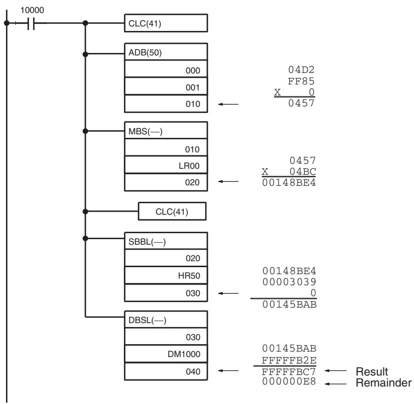
flowchart
graph TD
    A["10000"] --> B["CLC(41)"]
    A --> C["ADB(50)"]
    C --> D["000"]
    C --> E["001"]
    C --> F["010"]
    D --> G["04D2 FF85 X 0 0457"]
    E --> H["MBS(—)"]
    H --> I["010"]
    H --> J["LR00"]
    H --> K["020"]
    I --> L["0457 X 04BC 00148BE4"]
    K --> M["CLC(41)"]
    N["SBBL(—)"] --> O["020"]
    N --> P["HR50"]
    N --> Q["030"]
    R["DBSL(—)"] --> S["030"]
    R --> T["DM1000"]
    R --> U["040"]
    V["Result"] --> W["FFFFFB2E FFFFFBC7 000000E8"]
    W --> X["Remainder"]
SECTION 2
Inner Boards
This section describes software applications information for the following Inner Boards: High-speed Counter Board, Pulse I/O Board, Absolute Encoder Interface Board, Analog Setting Board, Analog I/O Board, and Serial Communications Board. Refer to the CQM1H Operation Manual for hardware information.
2-1 High-speed Counter Board 64
2-1-1 Model 64
2-1-2 Functions.... 64
2-1-3 Example System Configuration 64
2-1-4 Applicable Inner Board Slots 65
2-1-5 Names and Functions 65
2-1-6 Specifications 66
2-1-7 High-speed Counters 1 to 4 69
2-2 Pulse I/O Board.... 87
2-2-1 Model 87
2-2-2 Function 87
2-2-3 System Configuration.... 88
2-2-4 Applicable Inner Board Slot.... 89
2-2-5 Names and Functions 89
2-2-6 Specifications 90
2-2-7 High-speed Counters 1 and 2 95
2-2-8 Functions.... 105
2-2-9 Fixed Duty Factor Pulse Output 105
2-2-10 Variable Duty Factor Pulse Outputs 117
2-2-11 Determining the Status of Ports 1 and 2.... 120
2-2-12 Precautions When Using Pulse Output Functions ..... 121
2-3 Absolute Encoder Interface Board 121
2-3-1 Model 121
2-3-2 Functions.... 122
2-3-3 System Configuration.... 122
2-3-4 Applicable Inner Board Slots 123
2-3-5 Names and Functions 123
2-3-6 Absolute Encoder Input Specifications 124
2-3-7 High-speed Counter Interrupts 126
2-4 Analog Setting Board 135
2-4-1 Model 135
2-4-2 Function 135
2-4-3 Applicable Inner Board Slots 136
2-4-4 Names and Functions 136
2-4-5 Specifications 136
2-5 Analog I/O Board 137
2-5-1 Model 137
2-5-2 Function 137
2-5-3 System Configuration.... 137
2-5-4 Applicable Inner Board Slot.... 138
2-5-5 Names and Functions 138
2-5-6 Specifications 139
2-5-7 Application Procedure 141
2-6 Serial Communications Board 141
2-6-1 Model Number 141
2-6-2 Serial Communications Boards 141
2-6-3 Features.... 142
2-6-4 System Configuration.... 143
2-1 High-speed Counter Board
2-1-1 Model
| Name | Model | Specification |
| High-speed Counter Board | CQM1H-CTB41 | Four pulse inputsFour external outputs of comparison result |
2-1-2 Functions
The High-speed Counter Board is an Inner Board that handles four pulse inputs.
High-speed Counter Pulse Inputs 1 to 4
The High-speed Counter Board counts high-speed pulses from 50 to 500 kHz entering through ports 1 to 4, and performs tasks according to the number of pulses counted.
Input Modes
The following three Input Modes are available:
• Differential Phase Mode (1x/2x/4x)
- Up/Down Mode
- Pulse/Direction Mode
Comparison Operation
When the PV (present value) of the high-speed counter matches a specified target value or lies within a specified range, the bit pattern specified in the comparison table is stored in internal output bits and external output bits. A bit pattern can be set for each comparison result, and the external output bits can be output through an external output terminal as described below.
External Outputs
Up to four external outputs can be produced when either the target value is matched or a range comparison condition is satisfied.
Note The High-speed Counter Board does not provide high-speed counter interrupts. It simply compares the PV to target values or comparison ranges, and produces internal and external bit outputs.
2-1-3 Example System Configuration
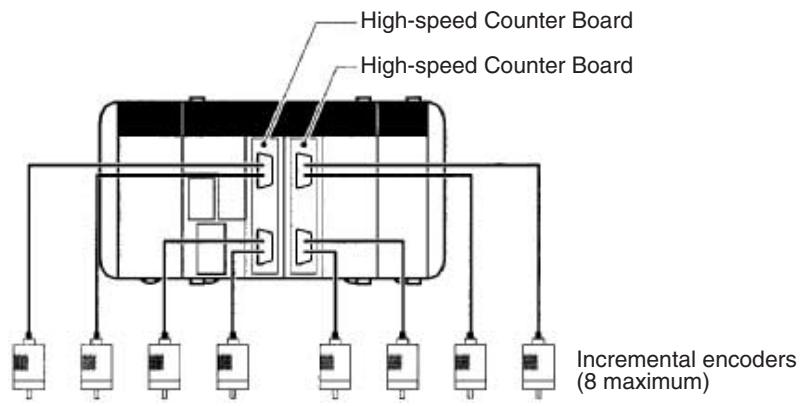
2-1-4 Applicable Inner Board Slots
The High-speed Counter Board can be installed in either slot 1 (left slot) or slot 2 (right slot) of the CQM1H-CPU51/61 CPU Unit. Both slots can be used at the same time.
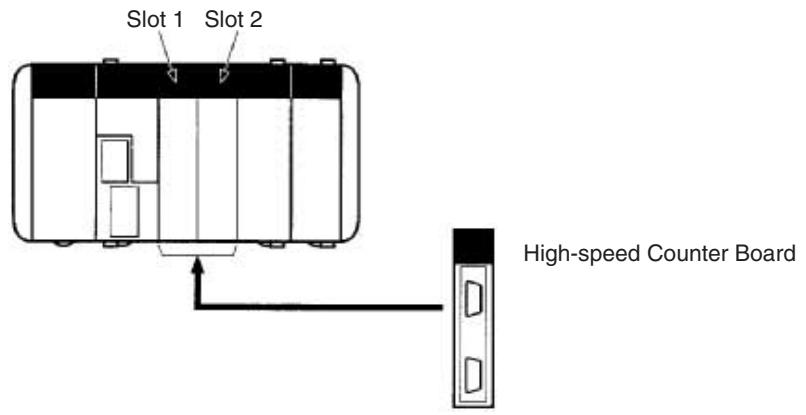
2-1-5 Names and Functions
One High-speed Counter Board provides two connectors that accept high-speed pulse inputs. CN1 is used for inputs 1 and 2, and CN2 is used for inputs 3 and 4.
CQM1H-CTB41 High-speed Counter Board
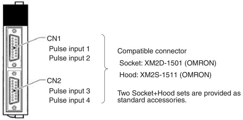
LED Indicators
RDY: Operational (Green)
Lit when pulse inputs can be received.
Pulse Inputs (Orange)
A1, A2, A3, A4:
Lit when phase-A input is ON in port 1, 2, 3, or 4.
B1, B2, B3, B4:
Lit when phase-B input is ON in port 1, 2, 3, or 4.
Z1, Z2, Z3, Z4:
Lit when phase-Z input is ON in port 1, 2, 3, or 4.
External Outputs (Orange)
OUT1, OUT2, OUT3, OUT4:
Lit when the corresponding output (1, 2, 3, or 4) is ON.
ERR: Error (Red)
Lit when an error is detected in the PC Setup settings for the input pulse function, or when an overflow or underflow occurs in the high-speed counter's present value.
2-1-6 Specifications
Instructions
| Instruction | Meaning |
| CTBL(63) | Used to register target or range comparison tables or used to start comparisons for previously registered comparison tables. A table can be registered and comparison started with separate instructions or the same instruction. |
| INI(61) | Used to start or stop comparison using registered comparison table or used to change the PV of a high-speed counter. |
| PRV(62) | Used to read the PV or status of a high-speed counter. |
Related Control Bits, Flags, and Status Information
| Word | Bits | Name | Function | ||
| Slot 1 | Slot 2 | ||||
| IR 200 | IR 232 | 00 to 15 | Counter 1 | PV (rightmost four digits) | The PV of the high-speed counter on each port of the High-speed Counter Board is stored after each cycle. Note The form in which data is stored (BCD or hexadecimal) can be specified in the PC Setup (DM 6602 and DM 6611). |
| IR 201 | IR 233 | 00 to 15 | PV (leftmost four digits) | ||
| IR 202 | IR 234 | 00 to 15 | Counter 2 | PV (rightmost four digits) | |
| IR 203 | IR 235 | 00 to 15 | PV (leftmost four digits) | ||
| IR 204 | IR 236 | 00 to 15 | Counter 3 | PV (rightmost four digits) | |
| IR 205 | IR 237 | 00 to 15 | PV (leftmost four digits) | ||
| IR 206 | IR 238 | 00 to 15 | Counter 4 | PV (rightmost four digits) | |
| IR 207 | IR 239 | 00 to 15 | PV (leftmost four digits) | ||
| IR 208: Counter 1 IR 209: Counter 2 IR 210: Counter 3 IR 211: Counter 4 | IR 240: Counter 1 IR 241: Counter 2 IR 242: Counter 3 IR 243: Counter 4 | 00 to 07 | Comparison Results: Internal Output Bits 00 to 07 | Contains the bit pattern specified by oper- and in CTBL(63) when a condition is satis-fied. | |
| 08 to 11 | Comparison Results: Bits for External Outputs 1 to 4 | Contains the bit pattern specified by oper- and in CTBL(63) when a condition is satis-fied. | |||
| 12 | Counter Operating Flag | 0: Stopped 1: Operating | |||
| 13 | Comparison Flag | Indicates whether or not a comparison is in progress. 0: Stopped 1: Operating | |||
| 14 | PV Overflow/Underflow Flag | Indicates whether or not an overflow or underflow has occurred. 0: Normal 1: Overflow or underflow has occurred | |||
| 15 | SV Error Flag | 0: Normal 1: Setting error | |||
| Word | Bits | Name | Function | |
| Slot 1 | Slot 2 | |||
| IR 212 | AR 05 | 00 | High-speed counter 1 Reset Bit | Phase Z and software reset0: Counter not reset on phase Z1: Counter reset on phase ZSoftware reset only0: Counter not reset0→1: Counter reset |
| 01 | High-speed counter 2 Reset Bit | |||
| 02 | High-speed counter 3 Reset Bit | |||
| 03 | High-speed counter 4 Reset Bit | |||
| 08 | High-speed Counter 1 Comparison Start Bit | 0 → 1: Comparison starts1 → 0: Comparison stops | ||
| 09 | High-speed Counter 2 Comparison Start Bit | |||
| 10 | High-speed Counter 3 Comparison Start Bit | |||
| 11 | High-speed Counter 4 Comparison Start Bit | |||
| 12 | High-speed Counter 1 Stop Bit | 0: Operation continues1: Operation stops | ||
| 13 | High-speed Counter 2 Stop Bit | |||
| 14 | High-speed Counter 3 Stop Bit | |||
| 15 | High-speed Counter 4 Stop Bit | |||
| IR 213 | AR 06 | 00 | External Output 1 Force-set Bit | 0: No effect on output status1: Forces output ON |
| 01 | External Output 2 Force-set Bit | |||
| 02 | External Output 3 Force-set Bit | |||
| 03 | External Output 4 Force-set Bit | |||
| 04 | External Output Force-set Enable Bit | 0: Force-setting of outputs 1 to 4 disabled1: Force-setting of outputs 1 to 4 enabled | ||
| SR 254 | 15 | Inner Board Error Flag | 0: No error1: ErrorTurns ON when an error occurs in an Inner Board mounted in slot 1 or slot 2. The error code for slot 1 is stored in AR 0400 to AR 0407 and the error code for slot 2 is stored in AR 0408 to AR 0415. | |
| AR 04 | 00 to 07 | Error code for Inner Board in slot 1 | 00 Hex: Normal01 or 02 Hex: Hardware error03 Hex: PC Setup error | |
| 08 to 15 | Error code for Inner Board in slot 2 | |||
Related PC Setup Settings
| Word | Bits | Function | When setting is read | |
| Slot 1 | Slot 2 | |||
| DM 6602 | DM 6611 | 00 to 03 | Data format in which PVs of high-speed counters 1 to 4 are stored0: Eight-digit hexadecimal (BIN)1: Eight-digit BCD | When power is turned ON. |
| 04 to 07 | Not used. | |||
| 08 to 11 | Sourcing/Sinking setting for external outputs 1 to 40: Sourcing (PNP)1: Sinking (NPN) | |||
| 12 to 15 | Not used. | |||
| DM 6640 | DM 6643 | 00 to 03 | Input Mode for high-speed counter 10 Hex: 1x Differential phase input1 Hex: 2x Differential phase input2 Hex: 4x Differential phase input3 Hex: Up/Down pulse input4 Hex: Pulse/Direction input | When operation starts. |
| 04 to 07 | Count frequency, Numeric Range Mode and counter reset method of high-speed counter 1. Refer to the following table. | |||
| 08 to 11 | Input Mode of high-speed counter 2(Refer to the explanation given above for high-speed counter 1.) | |||
| 12 to 15 | Count frequency, Numeric Range Mode, and counter reset method of high-speed counter 2(Refer to the explanation given above for high-speed counter 1.) | |||
| DM 6641 | DM 6644 | 00 to 03 | Input Mode of high-speed counter 3(Refer to the explanation given above for high-speed counter 1.) | |
| 04 to 07 | Count frequency, Numeric Range Mode, and counter reset method of high-speed counter 3(Refer to the explanation given above for high-speed counter 1.) | |||
| 08 to 11 | Input Mode of high-speed counter 4(Refer to the explanation given above for high-speed counter 1.) | |||
| 12 to 15 | Count frequency, Numeric Range Mode, and counter reset method of high-speed counter 4(Refer to the explanation given above for high-speed counter 1.) | |||
Count Frequency, Numeric Range Mode, and Counter Reset Method of High-speed Counters
| Value | Count frequency | Numeric Range Mode | Counter reset method |
| 0 Hex | 50 KHz | Linear Mode | Phase Z + software reset |
| 1 Hex | Software reset only | ||
| 2 Hex | Ring Mode | Phase Z + software reset | |
| 3 Hex | Software reset only | ||
| 4 Hex | 500 KHz | Linear Mode | Phase Z + software reset |
| 5 Hex | Software reset only | ||
| 6 Hex | Ring Mode | Phase Z + software reset | |
| 7 Hex | Software reset only |
2-1-7 High-speed Counters 1 to 4
The High-speed Counter Board counts pulse signals entering through ports 1 to 4 from rotary encoders and outputs internal/external output bit patterns according to the number of pulses counted. The four ports can be used independently. An outline of the processing performed by high-speed counters 1 to 4 is provided below.
Overview of Process
Input Signals and Input Modes
High-speed counters 1 to 4 can be set to different Input Modes in response to the type of signal input.
Differential Phase Mode (Counting Speed: 25 kHz or 250 kHz)
Two phase signals (phase A and phase B) with phase difference multiples of 1x, 2x, or 4x are used together with a phase-Z signal for inputs. The count is incremented or decremented according to differences in the two phase signals.
Up/Down Mode (Counting Speed: 50 kHz or 500 kHz)
Phase A is the incrementing pulse and phase B is the decrementing pulse. The counter increments or decrements according to the pulse that is detected.
Pulse/Direction Mode (Counting Speed: 50 kHz or 500 kHz)
Phase A is the pulse signal and phase B is the direction signal. The counter increments when the phase-B signal is ON and decrements when it is OFF.
Differential Phase Mode
| Phase A | Phase B | 1x | 2x | 4x |
| ↑ | L | Increment | Increment | Increment |
| H | ↑ | --- | --- | Increment |
| ↓ | H | --- | Increment | Increment |
| L | ↓ | --- | --- | Increment |
| L | ↑ | --- | --- | Decrement |
| ↑ | H | --- | Decrement | Decrement |
| H | ↓ | --- | --- | Decrement |
| ↓ | L | Decrement | Decrement | Decrement |
other
| Encoder Input | State | Value | | ------------- | ----- | ----- | | Upper Input | Increment | 1 | | Upper Input | Decrement | 2 | | Lower Input | Increment | 3 | | Lower Input | Decrement | 2 | | Down Input | Increment | 1 | | Down Input | Decrement | 2 |
Numeric Ranges
The values counted by high-speed counters 1 to 4 can be counted using the following two range settings:
Ring Mode
In Ring Mode, the maximum value of a numerical range can be set using CTBL(63), and when the count is increment beyond this maximum value, it returns to zero. The count never becomes negative. Similarly, if the count is decremented from 0, it returns to the maximum value. The number of points on the ring is determined by setting the maximum value (i.e., the ring value) to a value between 1 and 8388607 BCD or between 1 and 7FFFFFFF Hex. When the maximum value is set to 8388607, the range will be 0 to 8388607 BCD.
Linear Mode
In Linear Mode, the count range is always -8388608 to 8388607 BCD or F8000000 to 07FFFFFF Hex. If the count decrements below -8388608 BCD or F8000000 Hex, an underflow is generated, and if it increments above 8388607 BCD or 07FFFFFF Hex, an overflow is generated.
flowchart
graph TD
    A["Max. count value (Ring value)"] --> B["0"]
    B --> C["Decrement"]
    C --> D["Increment"]
If an overflow occurs, the PV of the count will remain at 08388607 BCD or 07FFFFFF Hex, and if an underflow occurs, it will remain at F8388608 BCD or F8000000 Hex. In either case, counting and comparison will stop, but the comparison table will be retained in memory. The PV Overflow/Underflow Flag shown below will turn ON to indicate the underflow or overflow.
| Counter | PV Overflow/Underflow Flag | |
| Slot 1 | Slot 2 | |
| High-speed counter 1 | IR 20814 | IR 24014 |
| High-speed counter 2 | IR 20914 | IR 24114 |
| High-speed counter 3 | IR 21014 | IR 24214 |
| High-speed counter 4 | IR 21114 | IR 24314 |
When restarting the counting operation, use the reset methods given below to reset high-speed counters 1 and 2. (Counters will be reset automatically when program execution starts and finishes.)
Reset Methods
The following two methods can be set to determine the timing at which the PV of the counter is reset (i.e., set to 0):
- Phase-Z signal + software reset
- Software reset
Phase-Z Signal (Reset Input) + Software Reset
The PV of the high-speed counter is reset in the first rising edge of the phase-Z signal after the corresponding High-speed Counter Reset Bit (see below) turns ON.
Software Reset
The PV is reset when the High-speed Counter Reset Bit turns ON. There are separate Reset Bits for each high-speed counter 1 to 4.
The Reset Bits of high-speed counters 1 to 4 are given in the following table.
| Counter | Reset Bit | |
| Slot 1 | Slot 2 | |
| High-speed counter 1 | IR 21200 | AR 0500 |
| High-speed counter 2 | IR 21201 | AR 0501 |
| High-speed counter 3 | IR 21202 | AR 0502 |
| High-speed counter 4 | IR 21203 | AR 0503 |
Reset Bits for high-speed counters 1 to 4 are refreshed only once each cycle. A Reset Bit must be ON for a minimum of 1 cycle to be read reliably.
Note The comparison table registration and comparison execution status will not be changed when the PV is reset. If a comparison was being executed before the reset, it will continue.
Checking Methods for High-speed Counter Interrupts
The following two methods are available to check the PV of high-speed counters 1 to 4. (These are the same methods as those used for built-in high-speed counter 0.)
- Target value method
- Range comparison method
Refer to page 36 for a description of each method.
For the target value method, a maximum of 48 target values can be registered in the comparison table. When the PV of the counter matches one of the 48
registered target values, the corresponding bit pattern (1 to 48) will be output to specific bits in memory.

flowchart
graph TD
    A["PV of high-speed counter"] --> B["Comparison"]
    B --> C1["Target value (1)"]
    B --> C2["Target value (2)"]
    B --> C3["..."]
    B --> C4["Target value (48)"]
    C1 --> D1["Bit pattern (1)"]
    C2 --> D2["Bit pattern (2)"]
    C3 --> D3["..."]
    C4 --> D4["Bit pattern (48)"]
    D1 --> E["208 to 211/240 to 243 Wd"]
    D2 --> E
    D3 --> E
    D4 --> E
    E --> F1["External output bits: 11, 8, 7, 0"]
    F1 --> G1["Internal output bits (8 bits): An OR is taken of corresponding bits of IR 208 to IR 211, or IR 240 to IR 243. External outputs (four outputs)"]
    F1 --> G2["External outputs (four outputs)"]
When using target values, comparison is made to each target value in the order of the comparison table until all values have been met, and then comparison will return to the first value in the table. With the High-speed Counter Board, it does not make any difference if the target value is reached as a result of incrementing or decrementing the PV.
Note With high-speed counter 0 in the CPU Unit or high-speed counter 1 or 2 on the Pulse I/O Board or Absolute Encoder Interface Board, the leftmost bit of the word containing the subroutine number in the comparison table determines if target values are valid for incrementing or for decrementing the PV.
Examples of comparison table operation and bit pattern outputs are shown in the following diagrams.
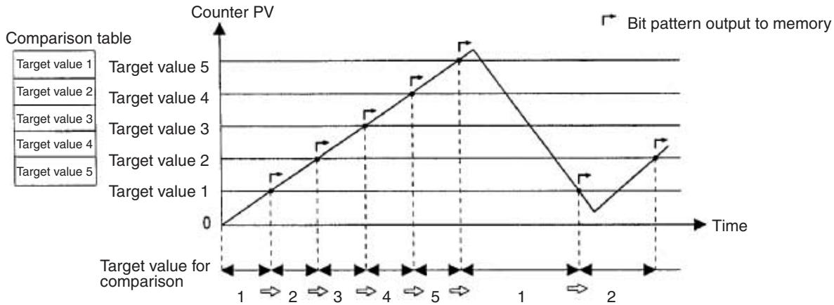
line
| Target value | Time | Counter PV | | ------------ | ---- | ---------- | | 1 | 1 | 0 | | 2 | 2 | 1 | | 3 | 3 | 2 | | 4 | 4 | 3 | | 5 | 5 | 5 | | 6 | 6 | 4 | | 7 | 7 | 3 | | 8 | 8 | 2 | | 9 | 9 | 1 | | 10 | 10 | 0 | | 11 | 11 | -1 | | 12 | 12 | -2 | | 13 | 13 | -3 | | 14 | 14 | -4 | | 15 | 15 | -5 | | 16 | 16 | -6 | | 17 | 17 | -7 | | 18 | 18 | -8 | | 19 | 19 | -9 | | 20 | 20 | -10 | | 21 | 21 | -11 | | 22 | 22 | -12 | | 23 | 23 | -13 | | 24 | 24 | -14 | | 25 | 25 | -15 | | 26 | 26 | -16 | | 27 | 27 | -17 | | 28 | 28 | -18 | | 29 | 29 | -19 | | 30 | 30 | -20 | | 31 | 31 | -21 | | 32 | 32 | -22 | | 33 | 33 | -23 | | 34 | 34 | -24 | | 35 | 35 | -25 | | 36 | 36 | -26 | | 37 | 37 | -27 | | 38 | 38 | -28 | | 39 | 39 | -29 | | 40 | 40 | -30 | | 41 | 41 | -31 | | 42 | 42 | -32 | | 43 | 43 | -33 | | 44 | 44 | -34 | | 45 | 45 | -35 | | 46 | 46 | -36 | | 47 | 47 | -37 | | 48 | 48 | -38 | | 49 | 49 | -39 | | 50 | 50 | -40 | | Note: The 'Target value' values are not explicitly labeled in the chart but are not provided in the data table. The 'Bit pattern output to memory' is indicated by arrows on the chart.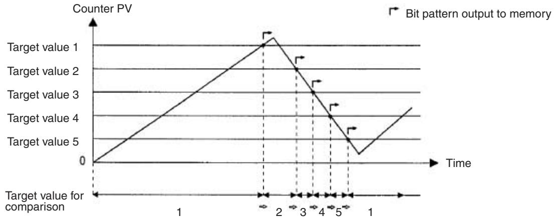
line
| Target value | Time | Counter PV | | ------------ | ---- | ---------- | | 1 | 2 | 1 | | 2 | 3 | 2 | | 3 | 4 | 1 | | 4 | 5 | 0 | | 5 | 6 | 1 |Comparison values 1 through 48 and bit patterns 1 through 48 are registered in the target value table. Of bits 00 to 11 of each of these bit patterns, bits 0 to 7 are stored as internal output bits, and bits 08 to 11 are stored as external output bits. As shown in the diagram below, the bits in the external bit pattern are used in an OR operation on the corresponding bits of high-speed counters 1 to 4, the results of which are then output as external outputs 1 to 4.
Example:
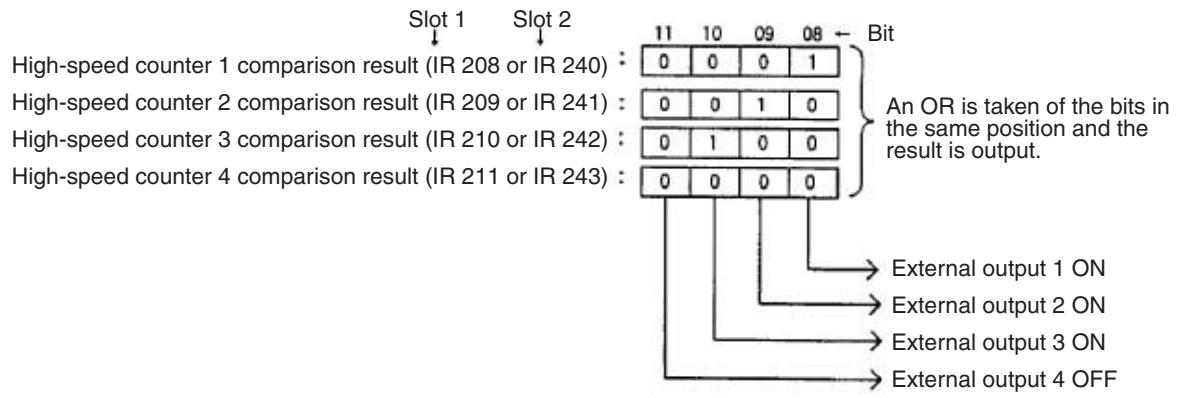
flowchart
graph TD
    A["Slot 1"] --> B["High-speed counter 1 comparison result (IR 208 or IR 240) : 0 0 0 1"]
    C["Slot 2"] --> D["High-speed counter 2 comparison result (IR 209 or IR 241) : 0 0 1 0"]
    E["Bit"] --> F["High-speed counter 3 comparison result (IR 210 or IR 242) : 0 1 0 0"]
    F --> G["High-speed counter 4 comparison result (IR 211 or IR 243) : 0 0 0 0"]
    G --> H["External output 1 ON"]
    G --> I["External output 2 ON"]
    G --> J["External output 3 ON"]
    G --> K["External output 4 OFF"]
    style A fill:#f9f,stroke:#333
    style C fill:#f9f,stroke:#333
    style E fill:#f9f,stroke:#333
    style F fill:#f9f,stroke:#333
    style G fill:#f9f,stroke:#333
    style H fill:#ccf,stroke:#333
    style I fill:#ccf,stroke:#333
    style J fill:#ccf,stroke:#333
    style K fill:#ccf,stroke:#333
For the range comparison method, 16 comparison ranges are registered in the comparison table. When the PV of the counter first enters between the upper and lower limits of one of the ranges 1 to 16, the corresponding bit pattern (1 to 16) will be output once to specific bits in memory.
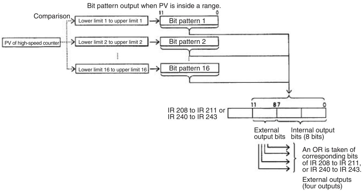
flowchart
graph TD
    A["PV of high-speed counter"] --> B["Comparison"]
    B --> C1["Lower limit 1 to upper limit 1"]
    B --> C2["Lower limit 2 to upper limit 2"]
    B --> C3["..."]
    B --> C16["Lower limit 16 to upper limit 16"]
    C1 --> D1["Bit pattern 1"]
    C2 --> D2["Bit pattern 2"]
    C3 --> D3["..."]
    C16 --> D16["Bit pattern 16"]
    D1 --> E["IR 208 to IR 211 or IR 240 to IR 243"]
    D2 --> E
    D3 --> E
    E --> F1["External output bits"]
    E --> F2["Internal output bits (8 bits)"]
    F1 --> G1["An OR is taken of corresponding bits of IR 208 to IR 211, or IR 240 to IR 243. External outputs (four outputs)"]
    F2 --> G2["External output bits"]
    F2 --> G3["Internal output bits (8 bits)"]
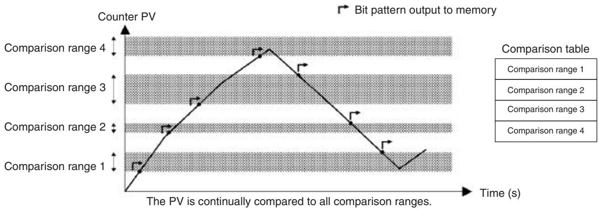
line
| Comparison Range | Time (s) | Counter PV | | ---------------- | -------- | ---------- | | Comparison range 1 | 0 | 0 | | Comparison range 2 | 1 | 1 | | Comparison range 3 | 2 | 2 | | Comparison range 4 | 3 | 3 | | Comparison range 1 | 4 | 4 | | Comparison range 2 | 5 | 5 | | Comparison range 3 | 6 | 6 | | Comparison range 4 | 7 | 7 | | The PV is continually compared to all comparison ranges. | 8 | 8 |Lower and upper limits for ranges 1 through 16 and bit patterns 1 through 16 are registered in the range comparison table. Of bits 0 to 11 of each of these bit patterns, bits 0 to 7 are stored as internal output bits, and bits 8 to 11 are stored as external output bits. As shown in the diagram below, the bits in the external bit pattern are used in an OR operation on the corresponding bits of high-speed counters 1 to 4, the results of which are then output as external outputs 1 to 4.
Example:
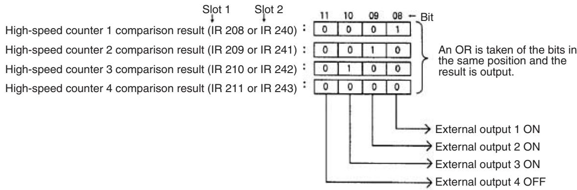
flowchart
graph TD
    A["Slot 1"] --> B["High-speed counter 1 comparison result (IR 208 or IR 240)"]
    C["Slot 2"] --> D["High-speed counter 2 comparison result (IR 209 or IR 241)"]
    E["Bit 11"] --> F["0 0 0 1"]
    G["Bit 10"] --> H["0 0 1 0"]
    I["Bit 09"] --> J["0 1 0 0"]
    K["Bit 08"] --> L["0 0 0 0"]
    M["Bit 0"] --> N["External output 1 ON"]
    O["Bit 1"] --> P["External output 2 ON"]
    Q["Bit 2"] --> R["External output 3 ON"]
    S["Bit 3"] --> T["External output 4 OFF"]
    U["Bit 0"] --> V["An OR is taken of the bits in the same position and the result is output."]
External outputs 1 to 4 are controlled by ORs performed on corresponding bits (i.e., bits with the same bit number) in the comparison result bits 08 to 11 for high-speed counters 1 to 4. The user must determine which outputs should be turned ON for each possible comparison result and set the bit patterns so that the OR operations will produce the desired result.
Note Range Comparison Flags are supported by the built-in high-speed counter (high-speed counter 0) and the Pulse I/O Board for ranges1 to 8. These flags, however, are not supported by the High-speed Counter Board. The internal bit patterns must be used to produce the same type of output result.
Reading High-speed Counter Status
The following two methods can be used to read the status of high-speed counters 1 to 4:
• Using CPU Unit memory words
- Using PRV(62)
Using CPU Unit Memory Words
The memory area words and bits in the CPU Unit that indicate the status of high-speed counters 1 to 4 are given below.
Inner Board Error Codes
| Word | Bits | Function | ||
| Slot 1 | Slot 2 | |||
| AR 04 | 00 to 07 | Slot 1 | The following 2-digit error codes are stored.00 Hex: Normal01 or 02 Hex: Hardware error03 Hex: PC Setup error | |
| 08 to 15 | Slot 2 | |||
Operating Status Words
| High-speed counter | Word | |
| Slot 1 | Slot 2 | |
| High-speed counter 1 | IR 208 | IR 240 |
| High-speed counter 2 | IR 209 | IR 241 |
| High-speed counter 3 | IR 210 | IR 242 |
| High-speed counter 4 | IR 211 | IR 243 |
The functions of the bits in each operating status word are as follows:
| Bits | Function |
| 00 to 07 | Comparison Results: Internal Output Bits |
| 08 to 11 | Comparison Results: External Output Bits for Outputs 1 to 4The result of an OR operation on bits in same bit positions for all the high-speed counters 1 to 4 will be output. (See note.) |
| 12 | Counter Operating Flag (0: Stopped; 1: Running) |
| 13 | Comparison Flag (0: Stopped; 1: Running) |
| 14 | PV Overflow/Underflow Flag (0: No; 1: Yes) |
| 15 | SV Error Flag (0: Normal; 1: Error) |
Note The following table shows the relationship between external outputs 1 to 4 and Comparison Results External Output Bits.
| High-speed counter | External output | Slot 1 | Slot 2 |
| Counter 1 | External output 1 | OR of bits 08 of IR 208 to IR 211 | OR of bits 08 of IR 240 to IR 241 |
| Counter 2 | External output 2 | OR of bits 09 of IR 208 to IR 211 | OR of bits 09 of IR 240 to IR 241 |
| Counter 3 | External output 3 | OR of bits 10 of IR 208 to IR 211 | OR of bits 10 of IR 240 to IR 241 |
| Counter 4 | External output 4 | OR of bits 11 of IR 208 to IR 211 | OR of bits 11 of IR 240 to IR 241 |
Using PRV(62)
The status of high-speed counters 1 to 4 can be read using PRV(62) in the manner shown below.

P: Port specifier
C: 001
D: First destination word
| High-speed counter | Value specified in P | |
| Slot 1 | Slot 2 | |
| High-speed counter 1 | 101 | 001 |
| High-speed counter 2 | 102 | 002 |
| High-speed counter 3 | 103 | 003 |
| High-speed counter 4 | 104 | 004 |
The meaning of the individual bits of D, in which the status of high-speed counters 1 to 4 is stored, is given in the following table.
| Bits | Function |
| 00 to 07 | Comparison Results: Internal Output Bits |
| 08 to 11 | Comparison Results: External Output Bits for Outputs 1 to 4The result of an OR operation on bits in same bit positions for all the high-speed counters 1 to 4 will be output. (See also note.) |
| 12 | Counter Operating Flag (0: Stopped; 1: Running) |
| 13 | Comparison Flag (0: Stopped; 1: Running) |
| 14 | PV Overflow/Underflow Flag (0: No; 1: Yes) |
| 15 | SV Error Flag (0: Normal; 1: Error) |
Procedure for Using High-speed Counters
Determine counting rate, Input Mode, reset method, Numeric Range Mode, form in which PV of high-speed counter data is stored, and external output method.
Counting rate: 50 kHz/500 kHz
Input Modes:
Differential Phase Mode; Pulse/Direction Mode; Up/Down Mode
Reset methods: Phase Z + software reset; software reset
Numeric Range Modes: Ring Mode or Linear Mode
Form in which PV of high-speed counter data is stored:
8-digit BCD or 8-digit hexadecimal
External output method:
Sourcing or Sinking switching of transistor output
flowchart
graph TD
    A["Set input voltages (switches on Board)."] --> B["Mount Board and wire inputs."]
    B --> C
PC Setup
(Slot 1: DM 6602, DM 6640, DM 6641
Slot 2: DM 6611, DM 6643, DM 6644)
Counting rate: 50 kHz/500 kHz
Input Modes:
Differential Phase Mode; Up/Down Mode; Pulse/Direction Mode
Reset methods:
Phase Z + software reset; software reset
Numeric Ranges: Ring Mode or Linear Mode
External output method:
Sourcing or Sinking switching of transistor output
Form in which PV of high-speed counter data is stored:
8-digit BCD; 8-digit hexadecimal
flowchart
graph TD
    A["Determine count check (comparison) method and internal/external bit patterns."] --> B["↓"]
Ladder program
Count check methods: Target value or range comparison
Output bit patterns when conditions met:
Internal and external output bits
REGISTER COMPARISON TABLE (CTBL(63)):
Port specification; comparison table registration; comparison start
MODE CONTROL (INI(61)):
Port specification; PV change; comparison start
HIGH-SPEED COUNTER PV READ (PRV(62)):
Reading PV of high-speed counter and status of comparison.
High-speed Counter Function
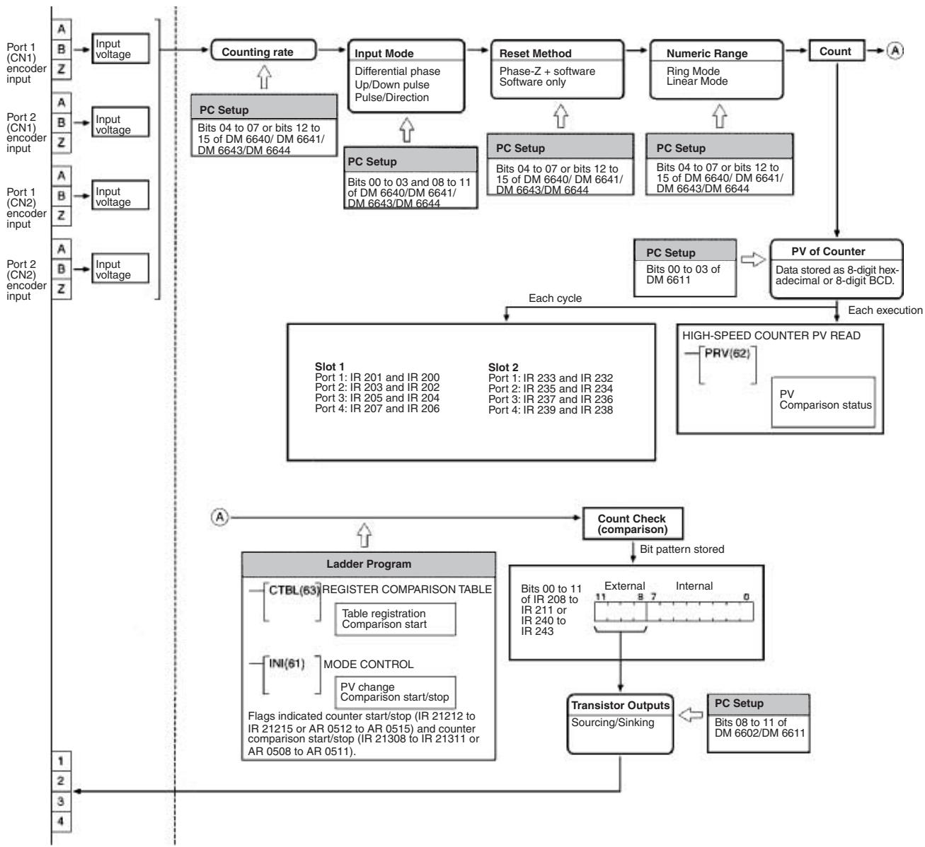
flowchart
graph TD
    A["Port 1 (CN1) encoder input"] --> B["Input voltage"]
    C["Port 2 (CN1) encoder input"] --> D["Input voltage"]
    E["Port 1 (CN2) encoder input"] --> F["Input voltage"]
    G["Port 2 (CN2) encoder input"] --> H["Input voltage"]
    B --> I["Counting rate"]
    D --> J["PC Setup"]
    D --> K["PC Setup"]
    I --> L["Input Mode"]
    J --> M["Reset Method"]
    K --> N["Numeric Range"]
    L --> O["PC Setup Differential phase Up/Down pulse Pulse/Direction"]
    M --> P["PC Setup Bits 04 to 07 or bits 12 to 15 of DM 6640/DM 6641/DM 6643/DM 6644"]
    N --> Q["PC Setup Bits 04 to 07 or bits 12 to 15 of DM 6640/DM 6641/DM 6643/DM 6644"]
    Q --> R["PC Setup Bits 04 to 07 or bits 12 to 15 of DM 6640/DM 6641/DM 6643/DM 6644"]
    R --> S["Count"]
    S --> T["A"]
    U["Port 1 (CN2) encoder input"] --> V["Input voltage"]
    W["Port 2 (CN2) encoder input"] --> X["Input voltage"]
    Y["Port 1 (CN1) encoder input"] --> Z["Input voltage"]
    AA["Port 2 (CN1) encoder input"] --> AB["Input voltage"]
    AC["Port 1 (CN1) encoder input"] --> AD["Input voltage"]
    AE["Port 2 (CN1) encoder input"] --> AF["Input voltage"]
    AG["Port 1 (CN2) encoder input"] --> AH["Input voltage"]
    AI["Port 2 (CN2) encoder input"] --> AJ["Input voltage"]
    AK["Port 1 (CN2) encoder input"] --> AL["Input voltage"]
    AM["Port 2 (CN2) encoder input"] --> AN["Input voltage"]
    AO["Port 1 (CN2) encoder input"] --> AP["Input voltage"]
    AQ["Port 2 (CN2) encoder input"] --> AR["Input voltage"]
    AS["Ladder Program"] --> AT["CTBL(63)"]
    AS --> AU["Register Comparison Table"]
    AS --> AV["Table registration Comparison start"]
    AS --> AW["INI(61)"]
    AS --> AX["MODE CONTROL"]
    AS --> AY["PV change Comparison start/stop"]
    AS --> AZ["Flags indicated counter start/stop (IR 21212 to IR 21215 or AR 0512 to AR 0515) and counter comparison start/stop (IR 21308 to IR 21311 or AR 0508 to AR 0511)."]
    AS --> BA["Sourcing/Sinking"]
    BB["High-Speed Counter PV READ"] --> BC["PRV(62)"]
    BD["PV Comparison status"] --> BE["Data stored as 8-digit hexadecimal or 8-digit BCD."]
    BC --> BF["Each cycle"]
    BF --> BG{Each execution}
    BG --> BH{Each cycle}
    BH --> BI["PV of Counter"]
    BI --> BJ{Each cycle}
    BJ --> BK["High-Speed Counter PV READ"]
    BK --> BL["PV Comparison status"]
    BM["Count Check (comparison)"] --> BN["Bit pattern stored"]
    BN --> BO["Transistor Outputs"]
    BO --> BP["Sourcing/Sinking"]
    BP --> BQ["PC Setup Bits 08 to 11 of DM 6602/DM 6611"]
Preliminary PC Setup Settings
To use high-speed counters 1 to 4, make the following settings in PROGRAM mode.
Data Format and Sourcing/Sinking Setting for External Outputs
Slot 1: DM 6602
Slot 2: DM 6611
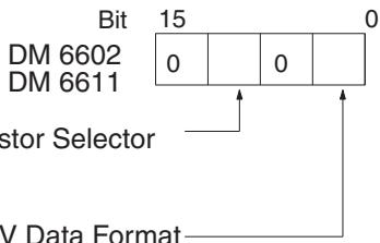
External Outputs 1 to 4 Transistor Selector
0 Hex: Sourcing (PNP)
1 Hex: Sinking (NPN)
High-speed Counters 1 to 4 PV Data Format
0 Hex: 8-digit hexadecimal (BIN)
1 Hex: 8-digit BCD
Default: 0000 (8-digit hexadecimal and sourcing (PNP))
Input Mode, Count Frequency, Numeric Range Mode, and Counter Reset Method
High-speed counter 1
Slot 1: Bits 00 to 07 of DM 6640 Slot 2: Bits 00 to 07 of DM 6643
High-speed counter 2
Slot 1: Bits 08 to 15 of DM 6640 Slot 2: Bits 08 to 15 of DM 6643
High-speed counter 3
Slot 1: Bits 00 to 07 of DM 6641 Slot 2: Bits 00 to 07 of DM 6644
High-speed counter 4
Slot 1: Bits 08 to 15 of DM 6641 Slot 2: Bits 08 to 15 of DM 6644
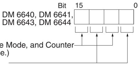
Count Frequency, Numeric Range Mode, and Counter Reset Method (See following table.)
High-speed Counter Input Mode
0 Hex: 1x Differential phase input
1 Hex: 2x Differential phase input
2 Hex: 4x Differential phase input
3 Hex: Up/Down pulse input
4 Hex: Pulse/Direction input
Default: 0000 (1x differential phase input, 50 kHz, Linear Mode, phase-Z + software reset)
Count Frequency,
Numeric Range Mode, and Reset Method
| Value | Count frequency | Numeric Range Mode | Counter reset method |
| 0 Hex | 50 KHz | Linear Mode | Phase Z + software reset |
| 1 Hex | Software reset only | ||
| 2 Hex | Ring Mode | Phase Z + software reset | |
| 3 Hex | Software reset only | ||
| 4 Hex | 500 KHz | Linear Mode | Phase Z + software reset |
| 5 Hex | Software reset only | ||
| 6 Hex | Ring Mode | Phase Z + software reset | |
| 7 Hex | Software reset only |
Usage
High-speed counters are programmed as follows:
- The count operation is started as soon as valid settings are made.
- The PV is reset to 0 when power is turned ON and when program execution is started or stopped.
- The count operation alone does not start the comparison operation with the comparison table.
- The PV can be monitored using the words shown in the following table.
| High-speed counter | Word | |
| Slot 1 | Slot 2 | |
| High-speed counter 1 | IR 200, IR 201 | IR 232, IR 233 |
| High-speed counter 2 | IR 202, IR 203 | IR 234, IR 235 |
| High-speed counter 3 | IR 204, IR 205 | IR 236, IR 237 |
| High-speed counter 4 | IR 206, IR 207 | IR 238, IR 239 |
Starting Comparison Operation
The comparison table is registered in the CQM1H and the comparison started with CTBL(63). Comparison can also be started using the relevant control bits (IR 21208 to IR 21211 for slot 1 AR 0508 to AR 0511 for slot 2).
Starting Comparison with CTBL(63)
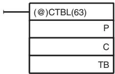
P: Port
C: Mode
000: Target value table registration and comparison start
001: Range comparison table registration and comparison start
002: Target value table registration only
003: Range comparison table registration only
TB: First word of comparison table
| High-speed counter | Value specified in P | |
| Slot 1 | Slot 2 | |
| High-speed counter 1 | 101 | 001 |
| High-speed counter 2 | 102 | 002 |
| High-speed counter 3 | 103 | 003 |
| High-speed counter 4 | 104 | 004 |
Setting 000 as the value of C registers a target value comparison table, and setting 001 registers a range comparison table. Comparison begins upon completion of this registration. While comparison is being executed, a bit pattern is stored as internal output bits and external output bits, as determined by the comparison table. Refer to the description of CTBL(63) for details on comparison table registration.
Note Although setting the value of C to 002 registers a target value comparison table, and setting C to 003 registers a range comparison table, comparison does not start automatically for these values. A control bit or INI(61) must be used to start the comparison operation.
Starting Comparison with Control Bits
The comparison operation will start when the bit corresponding to the high-speed counter in IR 21208 to IR 21211 for slot 1 or AR 0508 to AR 0511 for slot 2 is turned ON. It is necessary to have registered a comparison table beforehand. Comparisons cannot be performed in PROGRAM mode.
Note The High-speed Counter Board outputs the results of comparison as bit patterns to specific bits in memory, and does not execute interrupt subroutines.
Stopping Comparison Operation
Bit patterns consist of internal bits and external bits, and the external bits are output on external output 1 to 4.
To halt a comparison operation, execute INI(61) as shown below. Halting a comparison can also be accomplished using a control bit.
Stopping Comparison with INI(61)
| (@)INI(61) |
| P |
| 001 |
| 000 |
P: Port
| High-speed counter | Value set in P | |
| Slot 1 | Slot 2 | |
| High-speed counter 1 | 101 | 001 |
| High-speed counter 2 | 102 | 002 |
| High-speed counter 3 | 103 | 003 |
| High-speed counter 4 | 104 | 004 |
Stopping Comparison with Control Bits
The comparison operation will stop when the bit corresponding to the high-speed counter in IR 21208 to IR 21211 for slot 1 or AR 0508 to AR 0511 for slot 2 is turned OFF.
Note
- To restart a comparison, either execute INI(61) with the port number as the first operand and 000 (execute comparison) as the second operand, or change the status of the control bit from 0 to 1.
- Once a table has been registered, it is retained in the CQM1H throughout the operation (i.e., while a program is running) until a new table is registered.
Reading the PVs
The following two methods can be used to read the PVs of the high-speed counters 1 to 4:
- Reading the PV words in memory
- Using PRV(62)
Reading PV Words in Memory
The PVs of high-speed counters 1 to 4 are stored in memory in the following way. The form in which the PV data is stored is determined by the setting of bits 00 to 03 of DM 6602 for slot 1, and DM 6611 for slot 2. The default setting is 8-digit hexadecimal.
Slot 1:
Leftmost four digits
| Port 1 | IR 201 |
| Port 2 | IR 203 |
| Port 3 | IR 205 |
| Port 4 | IR 207 |
Rightmost four digits
| IR 200 |
| IR 202 |
| IR 204 |
| IR 206 |
Linear Mode
Ring Mode
8-digit Hex: F8000000 to 07FFFFFF Hex 00000000 to 07FFFFFF Hex
8-digit BCD: F8388608 to 08388607 00000000 to 08388607
(The leftmost digit will be F if the number is negative.)
Slot 2:
Leftmost four digits
| Port 1 | IR 233 |
| Port 2 | IR 235 |
| Port 3 | IR 237 |
| Port 4 | IR 239 |
Rightmost four digits
| IR 232 |
| IR 234 |
| IR 236 |
| IR 238 |
Linear Mode
Ring Mode
8-digit Hex: F8000000 to 07FFFFFF Hex 00000000 to 07FFFFFF Hex
8-digit BCD: F8388608 to 08388607 00000000 to 08388607
(The leftmost digit will be F if the number is negative.)
Note These words are refreshed only once every cycle, so the value read may differ slightly from the actual PV.
Using PRV(62)
PRV(62) can also be used to read the PVs of high-speed counters 1 to 4.
| (@)PRV(62) |
| P |
| C |
| D |
P: Port
C: 000
D: First destination word
| High-speed counter No. | Value specified in P | |
| Slot 1 | Slot 2 | |
| High-speed counter 1 | 101 | 001 |
| High-speed counter 2 | 102 | 002 |
| High-speed counter 3 | 103 | 003 |
| High-speed counter 4 | 104 | 004 |
The PVs of high-speed counters 1 to 4 are stored as shown in the following diagram.
Leftmost four digits
Rightmost four digits
Linear Mode
Ring Mode
D + 1
8-digit Hex: F8000000 to 07FFFFFF Hex
00000000 to 07FFFFFF Hex
8-digit BCD: F8388608 to 08388607 BCD
00000000 to 08388607 BCD
(The leftmost digit will be F if the number is negative.)
Note PRV(62) reads the current PV when it is executed.
Changing PVs
The following 2 methods can be used to change the PVs of high-speed counters 1 to 4:
- Reset the counter (i.e., setting the counter to 0) using one of the reset methods
- Using INI(61)
The following is an explanation of the use of INI(61). Refer to Reset Methods on page 71 for an explanation of the use of the reset methods.
Changing PV with INI(61)
INI(61) is used to change the PV of high-speed counters 1 to 4.
| (@)INI(61) |
| P |
| C |
| P1 |
P: Port specifier
C: 002
P1: First PV word
| High-speed counter No. | Value specified in P | |
| Slot 1 | Slot 2 | |
| High-speed counter 1 | 101 | 001 |
| High-speed counter 2 | 102 | 002 |
| High-speed counter 3 | 103 | 003 |
| High-speed counter 4 | 104 | 004 |
Leftmost four digits
Rightmost four digits
Ring Mode
Ring Mode
P1 + 1
P1
F8000000 to 07FFFFFF Hex F8388608 to 08388607 BCD
00000000 to 07FFFFFF Hex 00000000 to 08388607 BCD
(The leftmost digit will be F Hex if the number is negative.)
Stopping and Restarting the Counting Operation
Note After matching the final target value in a target value comparison table, the comparison process returns automatically to the first target value in the table. Therefore, following completion of a sequence of comparisons, the process can be repeated by initializing the PV.
It is possible to stop the counting operation of one of the high-speed counters 1 to 4 by turning ON a control bit. The PV of the counter will be retained.
The counting operation can be stopped by turning ON bits 12 to 15 of IR 212 for slot 1 or AR 05 for slot 2. These bits correspond to high-speed counters 1 to 4. Turn OFF these bits to restart the counting operation. The high-speed counter will restart from the value at which it was stopped.
Note The Counter Operating Flag can be used to determine whether the count operation is running or stopped (0: Stopped; 1: Operating).
| High-speed counter | Counter Operating Flag | |
| Slot 1 | Slot 2 | |
| High-speed counter 1 | IR 20812 | IR 24012 |
| High-speed counter 2 | IR 20912 | IR 24112 |
| High-speed counter 3 | IR 21012 | IR 24212 |
| High-speed counter 4 | IR 21112 | IR 24312 |
Examples
The following example illustrates the use of high-speed counter 1 on a High-speed Counter Board mounted in slot 2. Target value comparison is performed to turn ON bits in the internal/external bit patterns stored in memory according to the PV of the counter. The status of the internal output bits is used to control the frequency of a contact pulse output.
The Reset Bit is kept ON in the program so that the PV of the counter is reset on the phase Z signal after the last target value has been reached.
Before running the program, the PC Setup should be set as shown below, and the CQM1H restarted to enable the new setting in DM 6611.
DM 6611: 0001 (Sourcing outputs for external outputs 1 to 4, 8-digit BCD for PV storage of high-speed counters 1 to 4)
DM 6643: 0003 (High-speed counter 1: Count frequency of 50 kHz; Linear Mode; phase-Z signal + software reset; Up/Down Mode).
When the PV reaches 2500, IR 05000 will be turned ON and external output 1 will be turned ON.
When the PV reaches 7500, IR 05001 will be turned ON and external output 2 will be turned ON.
When the PV reaches 10000, IR 05002 will be turned ON and external output 3 will be turned ON.
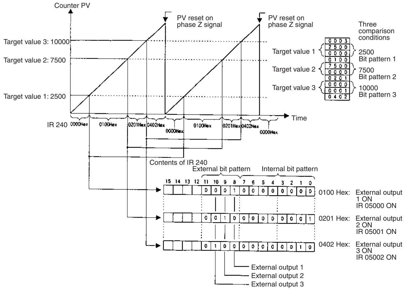
As shown in the following programming example, the frequency of the contact pulse output is changed from the value of 500 Hz set when CTBL(63) is executed to 200 Hz, 100 Hz, and then 0 Hz when IR 05000, IR 05001, and then IR 05002 turn ON.
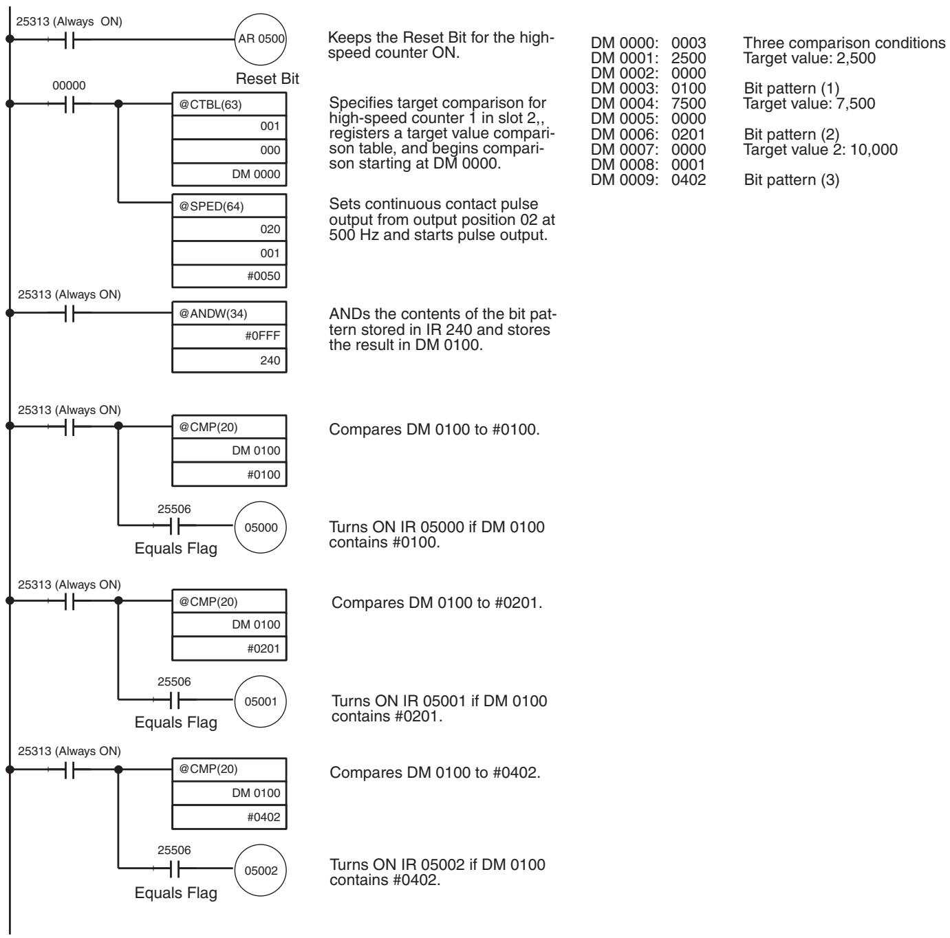
flowchart
graph TD
    A["25313 (Always ON)"] --> B["AR 0500"]
    B --> C["Reset Bit"]
    C --> D["@CTBL(63)"]
    D --> E["001"]
    D --> F["000"]
    D --> G["DM 0000"]
    G --> H["@SPED(64)"]
    H --> I["020"]
    H --> J["001"]
    H --> K["#0050"]
    K --> L["@ANDW(34)"]
    L --> M["#0FFF"]
    L --> N["240"]
    O["25313 (Always ON)"] --> P["@CMP(20)"]
    P --> Q["DM 0100"]
    P --> R["#0100"]
    R --> S["25506"]
    S --> T["05000"]
    T --> U["Equals Flag"]
    U --> V["@CMP(20)"]
    V --> W["DM 0100"]
    V --> X["#0201"]
    X --> Y["25506"]
    Y --> Z["05001"]
    Z --> AA["Equals Flag"]
    AA --> AB["@CMP(20)"]
    AB --> AC["DM 0100"]
    AB --> AD["#0402"]
    AD --> AE["25506"]
    AE --> AF["05002"]

    style A fill:#f9f,stroke:#333
    style O fill:#f9f,stroke:#333
    style O fill:#ccf,stroke:#333
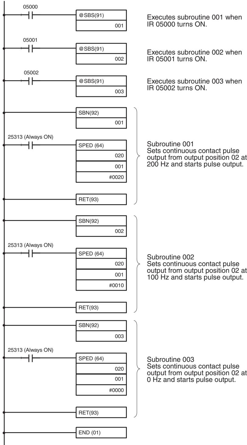
flowchart
graph TD
    A["05000"] --> B["@SBS(91)"]
    B --> C["001"]
    D["05001"] --> E["@SBS(91)"]
    E --> F["002"]
    G["05002"] --> H["@SBS(91)"]
    H --> I["003"]
    J["25313 (Always ON)"] --> K["SPED (64)"]
    K --> L["020"]
    K --> M["001"]
    K --> N["#0020"]
    O["RET(93)"] --> P["SBN(92)"]
    P --> Q["001"]
    R["25313 (Always ON)"] --> S["SPED (64)"]
    S --> T["020"]
    S --> U["001"]
    S --> V["#0010"]
    W["RET(93)"] --> X["SBN(92)"]
    X --> Y["002"]
    Z["25313 (Always ON)"] --> AA["SPED (64)"]
    AA --> AB["020"]
    AA --> AC["001"]
    AA --> AD["#0010"]
    AE["RET(93)"] --> AF["SBN(92)"]
    AF --> AG["003"]
    AH["END (01)"] --> AI["SET continuous contact pulse output from output position 02 at 100 Hz and starts pulse output."]
    AJ["Executes subroutine 001 when IR 05000 turns ON."] --> AK
    AL["Executes subroutine 002 when IR 05001 turns ON."] --> AM
    AN["Executes subroutine 003 when IR 05002 turns ON."] --> AO
    AP["Subroutine 001 Sets continuous contact pulse output from output position 02 at 200 Hz and starts pulse output."] --> AQ
    AR["Subroutine 002 Sets continuous contact pulse output from output position 02 at 100 Hz and starts pulse output."] --> AS
    AT["Subroutine 003 Sets continuous contact pulse output from output position 02 at 0 Hz and starts pulse output."] --> AU
Operation will be as illustrated below when the program is executed.
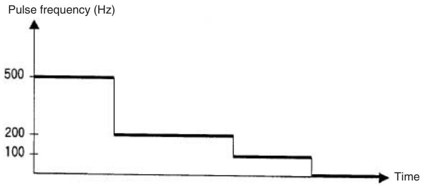
line
| Time | Pulse frequency (Hz) | | :--- | :--- | | 0 | 500 | | 1 | 200 | | 2 | 100 | | 3 | 50 |2-2 Pulse I/O Board
2-2-1 Model
| Name | Model | Specifications |
| Pulse I/O Board | CQM1H-PLB21 | Two pulse input points and two pulse output points |
2-2-2 Function
The Pulse I/O Board is an Inner Board that supports two pulse inputs and two pulse outputs.
Pulse Inputs 1 and 2
Pulse inputs 1 and 2 can be used as high-speed counters to count pulses input at either 50 kHz (signal phase) or 25 kHz (differential phase). Interrupt processing can be performed based on the present values (PV) of the counters.
Input Mode
The following three Input Modes are available:
• Differential Phase Mode (4x)
- Pulse/Direction Mode
- Up/Down Mode
Interrupts
The Board can be set to execute an interrupt subroutine when the value of the high-speed counter matches a specified target value, or an interrupt subroutine when the PV falls within a specified comparison range.
Pulse Outputs 1 and 2
Two 10 Hz to 50 kHz pulses can be output from port 1 and port 2. Both fixed and variable duty factors can be used.
- The fixed duty factor can raise or lower the frequency of the output from 10 Hz to 50 kHz smoothly.
- The variable duty factor enables pulse output to be performed using a duty factor ranging from 1% to 99%.
Note While pulse inputs and pulse outputs can be performed simultaneously, it is not possible to use all high-speed counter and pulse output functionality at the same time. The Port Mode Setting (High-speed Counter Mode/Simple Positioning Mode) in the PC Setup (DM 6611) will determine which has full functionality enabled.
Ports1 and 2
Two pulse inputs (high-speed counter) and two pulse outputs can be used simultaneously via ports 1 and 2. To determine which has functional priority, the appropriate Port Mode setting must be entered in the PC Setup (DM 6611).
| Mode | Content | High-speed counter functions | Pulse output functions | DM 6611 setting | |||
| Reading PV with PRV(62) | High-speed counter interrupts with CTBL(63) | No trapezoidal acceleration/ deceleration (SPED(64)) | Identical acceleration/ deceleration rates (PLS2(—)) | Separate acceleration/ deceleration rates (ACC(—)) | |||
| High-speed Counter Mode | High-speed counter given priority. All high-speed counter functions are enabled. Trapezoidal acceleration/ deceleration for pulse outputs is limited. | Yes | Yes | Yes | Mode 0 disabled (Modes 1 to 3 enabled) See note 1. | 0000 Hex | |
| Simple Positioning Mode | Pulse output given priority. All pulse output functions are enabled. Interrupts for the high-speed counter are disabled. | Yes | No | Yes | Yes | Yes | 0001 Hex |
Note
- Mode 0: Acceleration + Independent Mode; Mode 1: Acceleration + Continuous Mode; Mode 2: Deceleration + Independent Mode; Mode 3: Deceleration + Continuous Mode.
- The port modes for both ports 1 and 2 is always set to the same mode, i.e., either High-speed Counter Mode and Simple Positioning Mode. The mode cannot be set separately for each port.
2-2-3 System Configuration
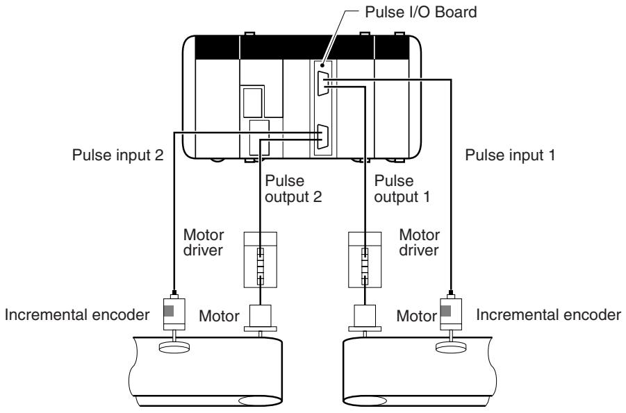
flowchart
graph TD
    A["Pulse I/O Board"] --> B["Pulse input 1"]
    A --> C["Pulse output 1"]
    A --> D["Pulse input 2"]
    D --> E["Motor driver"]
    E --> F["Incremental encoder"]
    A --> G["Pulse output 2"]
    G --> H["Motor"]
    H --> I["Incremental encoder"]
    A --> J["Pulse input 1"]
    J --> K["Motor driver"]
    K --> L["Incremental encoder"]
2-2-4 Applicable Inner Board Slot
The Pulse I/O Board can only be mounted in slot 2 (right slot) of the CQM1H-CPU51/61 CPU Unit.

2-2-5 Names and Functions
The CQM1H-PLB21 Pulse I/O Board has a CN1 connector for pulse input 1 and pulse output 1, and a CN2 connector for pulse input 2 and pulse output 2.
CQM1H-PLB21 Pulse I/O Board
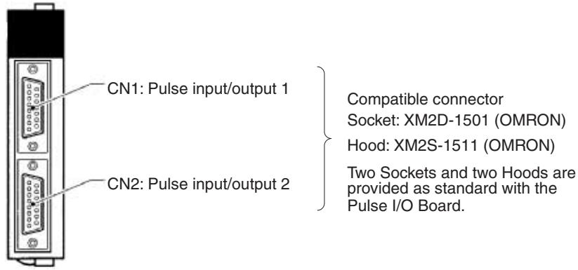
LED Indicators
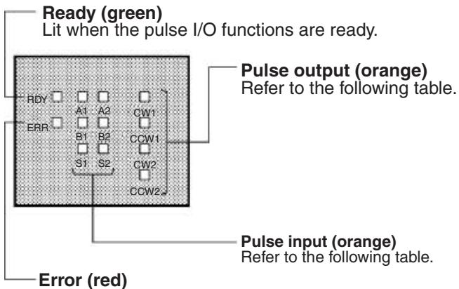
Lit when there is an error in the PC Setup settings for pulse I/O, or when operation is interrupted during pulse output.
Pulse Output Indicators
| Indicator | Port | Function |
| CW1 | Port 1 | Lit during CW pulse output to port 1. |
| CCW1 | Lit during CCW pulse output to port 1. | |
| CW2 | Port 2 | Lit during CW pulse output to port 2. |
| CCW2 | Lit during CCW pulse output to port 2. |
Pulse Input Indicators
| Port 1 | Port 2 | Function |
| A1 | A2 | Lit when the phase-A pulse input is ON at the port. |
| B1 | B2 | Lit when the phase-B pulse input is ON at the port. |
| Z1 | Z2 | Lit when the phase-Z pulse input is ON at the port. |
2-2-6 Specifications
High-speed Counter Specifications
Instructions
| Instruction | Control | Meaning |
| (@)CTBL(63) | Range comparison table registration + comparison start | Registers range comparison table and starts comparison. |
| Target value table registration + comparison start | Registers target value table and starts comparison. | |
| Range comparison table registration | Registers range comparison table. | |
| Target value table registration | Registers target value table. | |
| (@)INI(61) | Comparison start | Starts comparison using registered comparison table. |
| Comparison stop | Stops comparison. | |
| PV change | Changes PV of high-speed counter. | |
| (@)PRV(62) | PV read | Reads PV of high-speed counter. |
| Status read | Reads status of high-speed counter. | |
| Range comparison result read | Reads range comparison result. | |
| (@)INT(89) | Masking all interrupts | asking all interrupts, such as input interrupts, interval timer interrupts, and high-speed counter interrupts. |
| Clearing interrupt masks | Clears masks from interrupts. |
Relevant Flags and Control Bits for Pulse Inputs
Bits for Slot 2 of Inner Board when Using Pulse I/O Board
| Word | Bits | Name | Function | |
| IR 232 | 00 to 15 | Port 1 | PV word (rightmost four digits) | The PV of the high-speed counter for each port of the Pulse I/O Board is stored as an 8-digit BCD value after each cycle. |
| IR 233 | 00 to 15 | PV word (leftmost four digits) | ||
| IR 234 | 00 to 15 | Port 2 | PV word (rightmost four digits) | |
| IR 235 | 00 to 15 | PV word (leftmost four digits) | ||
SR Area Bits
| Word | Bit | Name | Function |
| SR 252 | 01 | High-speed Counter 1 Reset Bit (port 1) | Phase Z and software reset0: Counter not reset on phase Z1: Counter reset on phase Z |
| 02 | High-speed Counter 2 Reset Bit (port 2) | Software reset only0: Counter not reset0→1: Counter reset |
AR Area Flags
| Word | Bit | Name | Function | ||
| AR 05 | 00 | Port 1 | High-speed Counter 1 Range Comparison Flags | ON when meeting first condition. | When the high-speed counter is used for range comparisons, a flag turns ON when the corresponding condition is met. |
| 01 | ON when meeting second condition. | ||||
| 02 | ON when meeting third condition. | ||||
| 03 | ON when meeting fourth condition. | ||||
| 04 | ON when meeting fifth condition. | ||||
| 05 | ON when meeting sixth condition. | ||||
| 06 | ON when meeting seventh condition. | ||||
| 07 | ON when meeting eighth condition. | ||||
| 08 | High-speed Counter 1 Comparison Flag | Indicates the status of the comparison operation.0: Stopped1: Running | |||
| 09 | High-speed Counter 1 Overflow/Underflow Flag | Indicates the overflow/underflow status of the PV.0: Normal (No overflow/underflow)1: Overflow/Underflow has occurred. | |||
| AR 06 | 00 | Port 2 | High-speed Counter 2 Range Comparison Flags | ON when meeting first condition. | When the high-speed counter is used in range comparison format, a flag turns ON when the corresponding condition is met. |
| 01 | ON when meeting second condition. | ||||
| 02 | ON when meeting third condition. | ||||
| 03 | ON when meeting fourth condition. | ||||
| 04 | ON when meeting fifth condition. | ||||
| 05 | ON when meeting sixth condition. | ||||
| 06 | ON when meeting seventh condition. | ||||
| 07 | ON when meeting eighth condition. | ||||
| 08 | High-speed Counter 2 Comparison Flag | Indicates the status of the comparison operation.0: Stopped1: Running | |||
| 09 | High-speed Counter 2 Overflow/Underflow Flag | Indicates the overflow/underflow status of the PV.0: Normal (No overflow/underflow)1: Overflow/Underflow has occurred. | |||
SR Area Flags
| Word | Bit | Function |
| SR 254 | 15 | Inner Board Error Flag |
AR Area Flags
| Word | Bit | Function |
| AR 04 | 08 to 15 | Error codes for Inner Board in slot 200 Hex: Normal01,02 Hex: Hardware error03 Hex: PC Setup error |
Relevant PC Setup Settings
| Word | Bits | Function | When activated | |
| DM 6611 | 00 to 15 | Port Mode Setting (for ports 1 and 2)0000 Hex: High-speed Counter Mode0001 Hex: Simple Positioning Mode | When power is turned ON. | |
| DM 6643 | 00 to 03 | Port 1 | High-speed counter input mode0 Hex: Differential phase input1 Hex: Pulse/Direction input2 Hex: Up/Down pulse input | When operation starts. |
| 04 to 07 | High-speed counter reset method0 Hex: Phase-Z signal + software reset1 Hex: Software reset | |||
| 08 to 11 | High-speed counter numeric range0 Hex: Linear Mode1 Hex: Ring Mode | |||
| 12 to 15 | (Setting for pulse output use.) | |||
| DM 6644 | 00 to 03 | Port 2 | High-speed counter input mode0 Hex: Differential phase input1 Hex: Pulse/Direction input2 Hex: Up/Down pulse input | |
| 04 to 07 | High-speed counter reset method0 Hex: Phase-Z signal + software reset1 Hex: Software reset | |||
| 08 to 11 | High-speed counter numeric range0 Hex: Linear Mode1 Hex: Ring Mode | |||
| 12 to 15 | (Setting for pulse outputs.) | |||
Pulse Output Specifications
Instructions
Pulse outputs are controlled using the seven instructions shown in the following table. The table also shows the relationship between the instruction and the type of pulse output.
| Instruction | Control summary | Single-phase pulse output without acceleration/ deceleration | Single-phase pulse output with same acceleration/ deceleration rates | Single-phase pulse output with separate acceleration/ deceleration rates | Variable duty factor pulse output |
| PULS(65) (SET PULSES) | Sets number of output pulses. | Yes (Independent Mode only) | --- | Yes (Independent Mode only) | --- |
| SPED(64) (SPEED OUTPUT) | Controls pulse outputs without acceleration/deceleration. | Yes | --- | --- | --- |
| PLS2(—) (PULSE OUTPUT) | Controls trapezoidal acceleration/ deceleration pulse outputs having same acceleration/deceleration rate. | --- | Yes | --- | --- |
| ACC(—) (ACCELERATION CONTROL) | Controls trapezoidal acceleration/ deceleration pulse outputs having separate acceleration/deceleration rate. | --- | --- | Yes | --- |
| PWM(—) (PULSE WITH VARIABLE DUTY FACTOR) | Controls variable duty factor pulse outputs. | --- | --- | --- | Yes |
| INI(61) (MODE CONTROL) | Halts pulse output. | Yes | Yes | Yes | Yes |
| PRV(62) (HIGH-SPEED COUNTER PV READ) | Reads pulse output status. | Yes | Yes | Yes | Yes |
Instructions Applicable during Output
Some instructions relating to pulse output cannot be altered once output has begun. The following table lists those instructions that can and cannot be executed to change pulse output after another instruction has been executed (i.e., while pulse output is being performed as a result of a former instruction).
| Instruction that started pulse output | Instruction used to change pulse output | ||||||||||
| SPED (Inde-pen-dent) | SPED (Contin-uous) | PULS (0 or 1: Pulse setting) | PULS (2 or 3: pulse acceleration/ deceleration setting) | PULS (4 or 5: No pulse setting) | PLS2 | ACC Mode 0 (Accel-eration + Inde-pen-dent) | ACC Mode 1 (Accel-eration + Con-tinuous) | ACC Mode 2 (Decel-eration + Inde-pen-dent) | ACC Mode 3 (Decel-eration + Con-tinuous) | PWM | |
| SPED(64) (Independent Mode | Enabled | --- | --- | --- | --- | --- | Enabled | --- | Enabled | --- | --- |
| SPED(64) (Continuous Mode) | Enabled | Enabled | Enabled | Enabled | --- | --- | --- | Enabled | --- | Enabled | --- |
| PULS(65) 0,1 (Pulse set-ting) | Enabled | Enabled | Enabled | Enabled | Enabled | Enabled | --- | Enabled | Enabled | Enabled | --- |
| PULS(65) 2,3 (Pulse accel-eration/decel-eration setting) | Enabled | Enabled | Enabled | Enabled | Enabled | Enabled | Enabled | Enabled | Enabled | Enabled | --- |
| PULS(65) 3,4 (No pulse set-ting) | --- | Enabled | Enabled | Enabled | Enabled | Enabled | --- | Enabled | --- | Enabled | --- |
| PLS2(—) | --- | --- | --- | --- | --- | --- | --- | --- | Enabled when stopped | --- | --- |
| ACC(—) Mode 0 (Acceleration + Indepen-dent) | --- | --- | --- | --- | --- | --- | --- | --- | Enabled | --- | --- |
| ACC(—) Mode 1 (Acceleration + Continuous) | --- | Enabled for constant speed | Enabled (see note) | Enabled (see note) | --- | --- | --- | Enabled for constant speed | --- | Enabled | --- |
| ACC(—) Mode 2 (Deceleration + Indepen-dent) | Enabled for constant speed | --- | --- | --- | --- | --- | --- | --- | Enabled | --- | --- |
| ACC(—) Mode 0 (Deceleration + Continuous) | --- | Enabled for constant speed | Enabled (see note) | Enabled (see note) | Enabled (see note) | --- | --- | Enabled for constant speed | --- | Enabled | --- |
| PWM(—) | --- | --- | --- | --- | --- | --- | --- | --- | --- | --- | Enabled |
Note The number of pulses can be changed, but the direction cannot be changed.
Relevant Flags and
Control Bits (for Pulse
Output)
Bits for Slot 2 of Inner Board when Using Pulse I/O Board
| Word | Bits | Name | Function | |
| IR 236 | 00 to 15 | Port 1 | PV word (rightmost four digits) | The PV of the pulse output associated with each port of the Pulse I/O Board is stored as an 8-digit BCD after each cycle.When pulse output is not used, these bits can be used as internal auxiliary bits. |
| IR 237 | 00 to 15 | PV word (leftmost four digits) | ||
| IR 238 | 00 to 15 | Port 2 | PV word (rightmost four digits) | |
| IR 239 | 00 to 15 | PV word (leftmost four digits) | ||
AR Area Flags
| Word | Bit | Name | Function | |
| AR 05 | 12 | Port 1 Pulse Output Flags | Deceleration Specified Flag | Indicates passage through deceleration point when deceleration is specified.0: Not specified1: Specified |
| 13 | Number of Pulses Specified Flag | Indicates whether or not the number of pulses has been set using PULS(65).0: Not specified1: Specified | ||
| 14 | Pulse Output Completed Flag | Indicates completion of the pulse output by SPED(64), PLS2(—), or ACC(—).0: Not completed1: Completed | ||
| 15 | Pulse Output In Progress Flag | Indicates the execution status of the pulse output.0: No pulse output1: Pulse output in progress | ||
| AR 06 | 12 | Port 2 Pulse Output Flags | Deceleration Specified Flag | Indicates passage through deceleration point when deceleration is specified.0: Not specified1: Specified |
| 13 | Number of Pulses Specified Flag | Indicates whether or not the number of pulses has been set using PULS(65).0: Not specified1: Specified | ||
| 14 | Pulse Output Completed Flag | Indicates completion of the pulse outputby SPED(64), PLS2(—), or ACC(—).0: Not completed1: Completed | ||
| 15 | Pulse Output In Progress Flag | Indicates the execution status of the pulse output.0: No pulse output1: Pulse output in progress | ||
Operation Timing Example
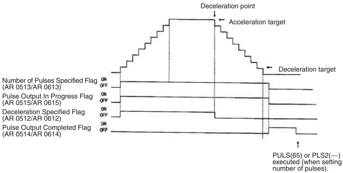
line
| Signal Type | Description | | --- | --- | | Pulse Output In Progress Flag | (AR 0515/AR 0615) | | Deceleration Specified Flag | (AR 0512/AR 0612) | | Pulse Output Completed Flag | (AR 0514/AR 0614) | | Number of Pulses Specified Flag | (AR 0513/AR 0613) | | Deceleration Target | (Deceleration point) | | PULS(65) or PLS2(--) executed (when setting number of pulses). | (PULS(65) or PLS2(--) executed (when setting number of pulses). |Note The status of the AR Area flags shown above may differ from the actual pulse output status due to the output frequency.
Relevant PC Setup Settings
| Word | Bit | Function | When setting is activated | |
| DM 6611 | 00 to 15 | Port Mode Setting (ports 1 and 2)0000 Hex: High-speed Counter Mode0001 Hex: Simple Positioning Mode | When power is turned ON. | |
| DM 6643 | 00 to 11 | Port 1 | (Setting for pulse input.) | When operation starts. |
| 12 to 15 | Fixed/Variable setting of pulse output duty factor0 Hex: Use fixed duty factor pulse output (default).1 Hex: Use variable duty factor pulse output. | |||
| DM 6644 | 00 to 11 | Port 2 | (Setting for pulse input.) | |
| 12 to 15 | Fixed/Variable setting of pulse output duty factor0 Hex: Use fixed duty factor pulse output (default).1 Hex: Use variable duty factor pulse output. | |||
2-2-7 High-speed Counters 1 and 2
Pulse signals from rotary encoders to ports 1 and 2 of the Pulse I/O Board can be counted at high speed, and interrupt processing can be executed according to the number of pulses counted. The two ports can be used independently, and the counters used for ports 1 and 2 are high-speed counter 1 and high-speed counter 2.
This section describes how to use high-speed counters 1 and 2.
Note The instructions that can be used are limited by the port mode setting of the Board, which is set in the DM 6611 of the PC Setup.
Port Mode Setting and Applicable Instructions
In Simple Positioning Mode, CTBL(63) (REGISTER COMPARISON TABLE) cannot be used, and high-speed counter interrupts cannot be performed. Only PV reads can be performed.
| Instruction | CTBL(63) | INI(61) | PRV(62) |
| Function | Comparison table registrationComparison start | PV changeComparison start/stop | PV readComparison status readRange comparison result read |
| High-speed Counter Mode | Enabled | Enabled | Enabled |
| Simple Positioning Mode | Disabled | Enabled (PV change only) | Enabled |
Processing
Input Signals and Input Modes
The Input Modes that can be used for high-speed counters 1 and 2 are determined by the signal types.
1,2,3...
- Differential Phase Mode (Counting Rate = 25 kHz):
Two phase-difference 4x signals (phase A and phase B) and a phase-Z signal are used for inputs. The count is incremented or decremented according to differences in the two phase signals.
- Pulse/Direction Mode (Counting Rate = 50 kHz):
Phase A is the direction signal and phase B is the count pulse. The counter increments when the phase-A signal is OFF and decrements when it is ON.
- Up/Down Mode (Counting Rate = 50 kHz):
Phase A is the decrementing signal and phase B is the incrementing signal. The counter decrements when an A-phase pulse is detected and increments when a phase-B pulse is detected.
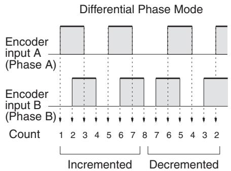
bar
| Encoder Input | Phase | Count | | ------------- | ----- | ----- | | Encoder input A | 1 | 1 | | Encoder input A | 2 | 2 | | Encoder input A | 3 | 3 | | Encoder input A | 4 | 4 | | Encoder input A | 5 | 5 | | Encoder input A | 6 | 6 | | Encoder input A | 7 | 7 | | Encoder input A | 8 | 8 | | Encoder input B | 1 | 1 | | Encoder input B | 2 | 2 | | Encoder input B | 3 | 3 | | Encoder input B | 4 | 4 | | Encoder input B | 5 | 5 | | Encoder input B | 6 | 6 | | Encoder input B | 7 | 7 | | Encoder input B | 8 | 8 | | Encoder input B (Decremented) | 1 | 1 | | Encoder input B (Decremented) | 2 | 2 | | Encoder input B (Decremented) | 3 | 3 | | Encoder input B (Decremented) | 4 | 4 | | Encoder input B (Decremented) | 5 | 5 | | Encoder input B (Decremented) | 6 | 6 | | Encoder input B (Decremented) | 7 | 7 | | Encoder input B (Decremented) | 8 | 8 | | Encoder input B (Decremented) | 1 | 1 | | Encoder input B (Decremented) | 2 | 2 | | Encoder input B (Decremented) | 3 | 3 | | Encoder input B (Decremented) | 4 | 4 | | Encoder input B (Decremented) | 5 | 5 | | Encoder input B (Decremented) | 6 - 8 | 6-8 | | Encoder input B (Decremented) | Dec - - - - - - - - - - - - - - - - - - - - - - - - - - - - - - - - - - - - - - - - - - - - - - - - - - - - - - - - - - - - - - - - - - - - - - - - - - - - - - - - - - - - - - - - - - - - - - - - - - - - 1 | Dec-1 |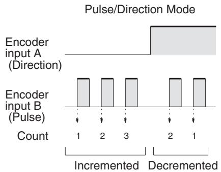
bar
| Encoder Input | Pulse Count | Time Interval | | ------------- | ----------- | ------------- | | Encoder input A (Direction) | 1 | 1 | | Encoder input A (Direction) | 2 | 2 | | Encoder input A (Direction) | 3 | 3 | | Encoder input B (Pulse) | 1 | 1 | | Encoder input B (Pulse) | 2 | 2 | | Encoder input B (Pulse) | 3 | 3 | | Encoder input B (Pulse) | 2 | 2 | | Encoder input B (Pulse) | 1 | 1 |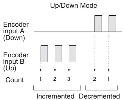
bar
| Encoder Input | Count | | ------------- | ----- | | A (Down) | 1 | | A (Down) | 2 | | A (Down) | 3 | | B (Up) | 1 | | B (Up) | 2 | | B (Up) | 3 | | C (Down) | 2 | | C (Down) | 1 |Numeric Ranges
The range of values counted by high-speed counters 1 and 2 are determined by the following two modes.
1,2,3...
- Ring Mode
In Ring Mode, the maximum value of the counting range can be set with CTBL(63). The counter will go from the maximum count value to 0 when incrementing, and from 0 to the maximum count value when decrementing; there are no negative values. The maximum count value + 1 (i.e., the ring value) is entered as the setting. Settings can range from 1 to 65,000, making the counting range 0 to 64,999.
- Linear Mode
The counting range in Linear Mode is fixed at -8,388,608 to 8,388,607. If
the count falls below the lower limit an underflow is generated, and if it exceeds the upper limit an overflow is generated. The PV will remain at 0838 8607 for overflows and F838 8608 for underflows, counting or comparison will be stopped (and the comparison table retained), and AR 0509 (port 1) or AR 0609 (port 2) will be turned ON.
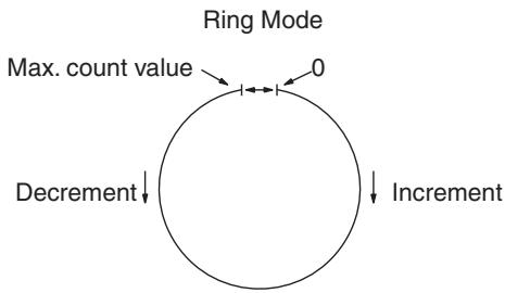
flowchart
graph TD
    A["0"] --> B["Ring Mode"]
    B --> C["Max. count value"]
    C --> D["Decrement"]
    D --> E["Increment"]
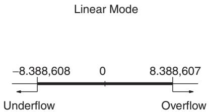
line
| Position | Value | | -------- | --------- | | Underflow | -8.388,608 | | 0 | 0 | | 8.388 | 8.388,607 |One of the methods in the following section should be used to reset the counter when restarting the counting operation. The counter will be reset automatically when program execution is started or stopped.
Note The following signal transitions are handled as forward (incrementing) pulses: Phase-A leading edge → phase-B leading edge → phase-A trailing edge → phase-B trailing edge.
The following signal transitions are handled as reverse (decrementing) pulses: Phase-B leading edge → phase-A leading edge → phase-B trailing edge → phase-A trailing edge.
Reset Methods
The following two methods can be used to determine the timing by which the PV of the counter is reset (i.e., set to 0):
- Phase-Z signal + software reset
- Software reset
Either the phase-Z signal + software reset or software reset alone may be used to reset the PV of the count. These resets operate in the same way as for high-speed counter 0 (the built-in high-speed counter). Refer to page 35 for details. The Reset Bits of high-speed counters 1 and 2 are as follows:
Reset Bit of high-speed counter 1: SR 25201
Reset Bit of high-speed counter 2: SR 25202
Note
- Since the reset bits for high-speed counters 1 and 2 (SR 25201 and SR 25202) are refreshed during each cycle, a flag must be ON for a minimum of 1 full cycle to be read reliably.
- Even after a reset, the comparison table registration status, comparison execution status, and range comparison results are retained unchanged. (If a comparison was being executed before the reset, it will continue.)
Just as for high-speed counter 0, the following two count check methods can be used for high-speed counters 1 and 2:
- Target value method
- Range comparison method
Refer to page 36 for a description of each method.
For the target value method, up to 48 conditions can be registered in the comparison table. When the PV of the counter matches one of the 48 registered comparison values, the corresponding interrupt subroutine will be executed.
For the range comparison method, 8 comparison conditions are always registered in the comparison table. When the PV of the counter lies within the upper and lower limits for one of the ranges 1 to 8, the corresponding interrupt subroutine will be executed.
Count Check Methods for High-speed Counter Interrupts
Procedure for Use
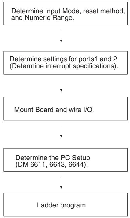
flowchart
graph TD
    A["Determine Input Mode, reset method, and Numeric Range."] --> B["Determine settings for ports1 and 2 (Determine interrupt specifications)."]
    B --> C["Mount Board and wire I/O."]
    C --> D["Determine the PC Setup (DM 6611, 6643, 6644)."]
    D --> E["Ladder program"]
Input Modes:
Differential Phase, Pulse/Direction, or Up/Down
Reset methods: Phase Z + software reset or Software reset
Numeric Range: Ring Mode or Linear Mode
Check method:
High-speed Counter Mode:
Target value interrupts, range comparison interrupts
Simple Positioning Mode:
No interrupts (PV read; range comparison result read)
Port Mode
Input Modes: Differential Phase, Pulse/Direction, Up/Down
Reset methods: Phase Z + software reset; Software reset
Numeric Range: Ring Mode; Linear Mode
REGISTER COMPARISON TABLE, CTBL(63):
Port-specific comparison table registration and comparison start
MODE CONTROL, INI(61):
Port-specific PV change and comparison start
HIGH-SPEED COUNTER PV READ, PRV(62):
Port-specific high-speed counter PV read, high-speed counter comparison status read, and range comparison result read
SUBROUTINE DEFINE, SBN(92) and RETURN, RET(93):
Creation of interrupt subroutines (Only when using high-speed counter 1 and 2 interrupts.)
Pulse I/O Board: High-speed Counter Function
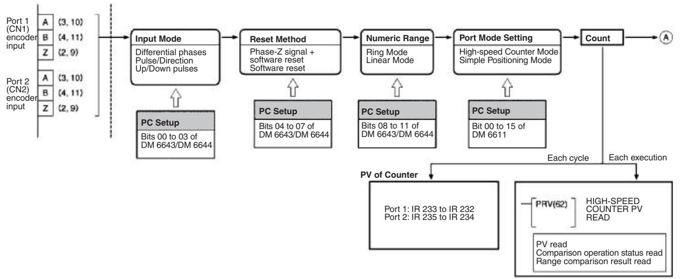
flowchart
graph TD
    A["Port 1 (CN1) encoder input"] --> B["Input Mode"]
    C["Port 2 (CN2) encoder input"] --> D["PC Setup"]
    B --> E["Reset Method"]
    E --> F["Numeric Range"]
    F --> G["Port Mode Setting"]
    G --> H["Count"]
    H --> I["A"]

    subgraph InputMode
        B1["Differential phases Pulse/Direction Up/Down pulses"]
        D1["Bits 00 to 03 of DM 6643/DM 6644"]
    end

    subgraph ResetMethod
        E1["Phase-Z signal + software reset Software reset"]
        F1["Bits 04 to 07 of DM 6643/DM 6644"]
    end

    subgraph NumericRange
        F1 --> G1["Ring Mode Linear Mode"]
        F2["Bits 08 to 11 of DM 6643/DM 6644"]
        G1 --> G2["High-speed Counter Mode Simple Positioning Mode"]
        G2 --> H
    end

    subgraph Count
        H --> I
    end

    J["PC Setup"] --> K["PV of Counter"]
    L["PC Setup"] --> M["PV read Comparison operation status read Range comparison result read"]

    N["Each cycle"] --> I
    O["Each execution"] --> I
    P["PRV(62)"] --> I
    Q["HIGH-SPEED COUNTER PV READ"] --> I
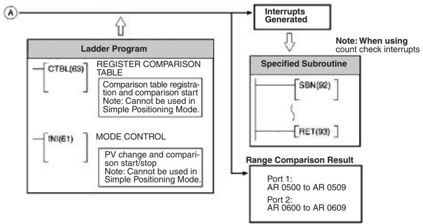
flowchart
graph TD
    A["Ladder Program"] --> B["Register Comparison Table"]
    A --> C["MODE CONTROL"]
    B --> D["Interrupts Generated"]
    C --> E["Range Comparison Result"]
    D --> F["Specified Subroutine"]
    E --> F
    style A fill:#f9f,stroke:#333
    style B fill:#ccf,stroke:#333
    style C fill:#cfc,stroke:#333
    style D fill:#fcc,stroke:#333
    style E fill:#cff,stroke:#333
    style F fill:#ffc,stroke:#333
Preliminary PC Setup
Before using high-speed counters 1 and/or 2, enter the following settings in PROGRAM mode.
Port Mode Setting (DM 6611)
Specify High-speed Counter Mode for ports 1 and 2. This setting is read when the PC is turned ON. If it is changed, the PC must be restarted.
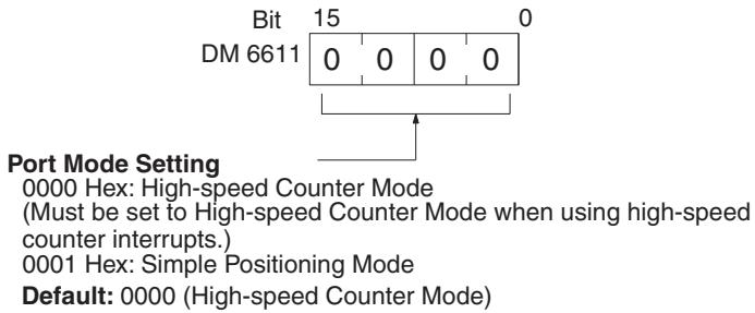
Note 1. When using high-speed counter 1 and 2 interrupts, the port must be set to High-speed Counter Mode. Although the PV of the high-speed counter can be read in Simple Positioning Mode, high-speed counter 1 and 2 interrupts cannot be used.
- This setting is only recognized when the CQM1H is started. To change the setting, turn the power OFF and then ON again before executing the program.
- If DM 6611 is used to set ports 1 and 2 to Simple Positioning Mode, it is possible to use the BCMP(68) instruction to check the contents of the PV words of high-speed counters 1 and 2 (IR 232 to IR 235) and use this information in place of high-speed counter 1 and 2 interrupts. However, the PV obtained using this method may vary slightly from the actual PV.
Port 1 and Port 2 Operation Settings
DM 6643 contains the settings for port 1, and DM 6644 contains the settings for port 2. These settings determine the operating parameters for these high-speed counters. Use settings that match the operating environment of each port.
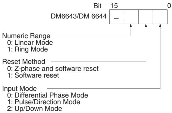
Default: 0000 (Linear Mode, Z-phase and software reset, Differential Phase) Mode
Input Refresh Word Settings
DM 6634 and DM 6635 contain the input refresh word settings for high-speed counters 1 and 2 respectively. Make these settings when it is necessary to refresh inputs before interrupt execution.
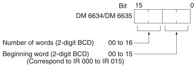
Default: 0000 (No input refresh)
Programming
Use the following steps to program high-speed counters 1 and 2.
Note
- High-speed counters 1 and 2 begin counting when the proper PC Setup settings are made.
- The PVs of high-speed counters 1 and 2 are reset to 0 when power is turned ON, when operation begins, and when operation stops.
- Comparison with the comparison table and interrupts will not be performed using the count operation alone.
- The PV of high-speed counter 1 is stored in IR 232 and IR 233, and the PV of high-speed counter 2 is stored in IR 234 and IR 235.
Starting and Stopping Comparison
1,2,3... 1. Use CTBL(63) to save the comparison table in the CQM1H and begin comparisons.
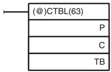
P: Port
001: Port 1 002: Port 2
C: Mode
000: Target value table registered and comparison begun 001: Range table registered and comparison begun 002: Target table registered only 003: Range table registered only
TB: Beginning word of comparison table
If C is set to 000, then comparisons will be made using the target value method; if 001, they will be made using the range comparison method. In both cases the comparisons will begin after the comparison table is registered. While comparisons are being performed, high-speed counter 1 and 2 interrupts will be executed according to the comparison table. Refer to the explanation of CTBL(63) in SECTION 5 Instruction Set for details on the contents of the comparison tables that are saved.
Note Although setting the value of C to 002 registers a target value comparison table, and setting C to 003 registers a range comparison table, comparison does not start automatically. In these cases, INI(61) must be used to start the comparison operation.
- To stop comparisons, execute INI(61) as shown below. Specify port 1 or 2 in P (P=001 or 002).
P: Port
001: Port 1 002: Port 2
Note 1. To restart comparisons, set the first operand to the port number, and the second operand to "000" (execute comparison), and execute the INI(61) instruction.
2. A table that has been registered will be retained in the CQM1H during operation (i.e., during program execution) until a new table is registered.
Reading the PV of High-speed Counters 1 and 2
The following two methods can be used to read the PVs of high-speed counters 1 and 2:
- Reading the PV from memory
- Using PRV(62)
Reading the PV from Memory
The PVs of high-speed counters 1 and 4 are stored in the corresponding data area words in the following way.
| Leftmost four digits | Rightmost four digits | Linear Mode | Ring Mode |
| Port 1: IR 233 | IR 232 | F8388608 to 08388607(-8,388,608 to 8,388,607) | 00000000 to 00064999 |
| Port 2: IR 235 | IR 234 | (The leftmost digit becomes F when the number is negative.) | |
Note These words are refreshed only once every cycle, so they may differ from the actual PV.
Using PRV(62)
PRV(62) is used to read the PVs of high-speed counters 1 and 2. Specify high-speed counter 1 or 2 in P (P=001 or 002).
P: Port
001: Port 1
002: Port 2
D: First destination word
The PV of each high-speed counter is stored as shown below. In Linear Mode, the leftmost bit will be F for negative values.
Leftmost four digits
Rightmost four digits
Linear Mode
Ring Mode


F8388608 to 08388607
00000000 to 0006499
(-8,388,608 to 8,388,607)
Note The PV can be read accurately at the time PRV(62) is executed.
Changing the PV
There are two ways to change the PV of high-speed counters 1 and 2.
- Resetting to 0 using one of the reset methods
- Using INI(61)
The method using INI(61) is explained here. Refer to Reset Methods on page 71 for an explanation of the use of the reset methods.
Changing the PV with INI(61)
Change the PV of high-speed counters 1 and 2 by using INI(61) as shown below.
P: Port
001: Port 1
002: Port 2
P1: First PV word
Leftmost four digits
Rightmost four digits
Linear Mode
Ring Mode


F8388608 to 08388607
00000000 to 0006499
To specify a negative number in Linear Mode, set F Hex in the leftmost digit.
Reading Status of High-speed Counters 1 and 2
There are 2 ways to read the status of high-speed counters 1 and 2:
- Reading the relevant flags in the AR area of the CQM1H
- Using PRV(62)
Reading the Relevant AR Area Flags
The CQM1H data words relating to high-speed counters 1 and 2 are shown below. It is possible to know the status of high-speed counters 1 and 2 by reading these words.
- Inner Board Error Codes
| Word | Bits | Function | |
| AR 04 | 08 to 15 | Slot2 | The stored error codes are as follows:00 Hex: Normal01, 02 Hex: Hardware error03 Hex: PC Setup error |
- Operating Status
| Word | Bit | Name | Function | ||
| Counter 1 | Counter 2 | ||||
| AR 05 | AR 06 | 00 | High-speed Counter Range Comparison Flags | ON when meeting first condition. | When the high-speed counter is used in range comparison format, a bit turns ON when the corresponding condition is met. |
| 01 | ON when meeting second condition. | ||||
| 02 | ON when meeting third condition. | ||||
| 03 | ON when meeting fourth condition. | ||||
| 04 | ON when meeting fifth condition. | ||||
| 05 | ON when meeting sixth condition. | ||||
| 06 | ON when meeting seventh condition. | ||||
| 07 | ON when meeting eighth condition. | ||||
| 08 | High-speed Counter Comparison Flag | Indicates the status of the comparison operation.0: Stopped1: Running | |||
| 09 | High-speed Counter Overflow/Underflow Flag | Indicates the overflow/underflow status of the PV.0: Normal (No overflow/underflow)1: Overflow/Underflow has occurred | |||
Using PRV(62)
The status of high-speed counters 1 and 2 can also be determined by executing PRV(62). Specify high-speed counter 1 or 2 (P=001 or 002) and the destination word D. The status information will be written to bits 00 and 01 of D. Bits 02 to 15 will be set to 0.
P: Port
001: Port 1
002: Port 2
D: Destination word
The status of the specified high-speed counter is stored in bits 00 and 01 of P1, as shown in the following table.
| Bit | Function |
| 00 | Comparison Operation Flag (0: Stopped; 1: Running) |
| 01 | High-speed Counter 1 and 2 PV Overflow/Underflow Flag (0: Normal; 1: Underflow or overflow occurred) |
Bits 04 to 07 indicate the pulse output status; all other bits are 0.
Example
This example shows a program that outputs standard pulses from port 1 while counting those pulses with high-speed counter 1. The high-speed counter operates in Up/Down Mode, with the pulse output's CW pulses incrementing the counter (B-phase input) and the CCW pulses decrementing the counter (A-phase input). Before executing the program, set the PC Setup as follows and restart the PC to enable the DM 6611 settings.
DM 6611: 0000 (High-speed Counter Mode).
DM 6643: 0002 (Port 1: Fixed duty factor pulse output, Linear Mode, Z-phase signal with software reset, and Up/Down Mode).
Other PC Setup settings use the default settings. (Inputs are not refreshed before interrupt processing.)
In addition, the following data is stored for the comparison table:
DM 0000: 0003 — Number of target values: 3
DM 0001: 2500 — Target value 1: 2,500
DM 0002: 0000
DM 0003: 0100 — Comparison 1 interrupt processing routine No.: 100
DM 0004: 7500 — Target value 2: 7,500
DM 0005: 0000
DM 0006: 0101 — Comparison 2 interrupt processing routine No.: 101
DM 0007: 0000 — Target value 3: 10,000
DM 0008: 0001
DM 0009: 0102 — Comparison 3 interrupt processing routine No.: 102
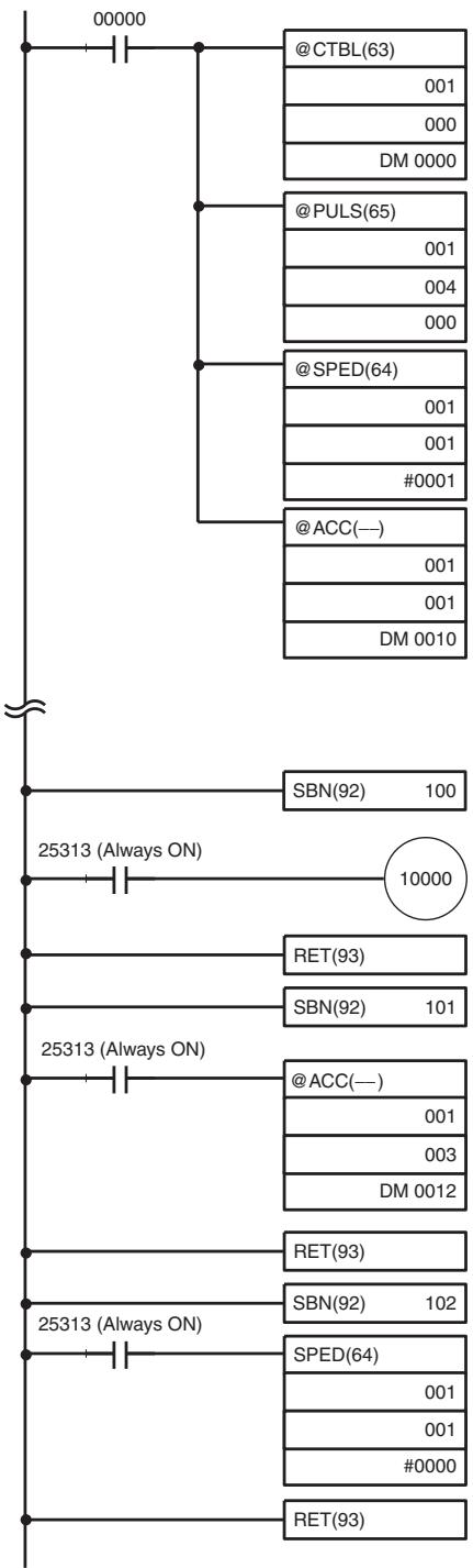
flowchart
graph TD
    A["00000"] --> B["@CTBL(63)"]
    B --> C["001"]
    B --> D["000"]
    B --> E["DM 0000"]
    A --> F["@PULS(65)"]
    F --> G["001"]
    F --> H["004"]
    F --> I["000"]
    A --> J["@SPED(64)"]
    J --> K["001"]
    J --> L["#0001"]
    A --> M["@ACC(---)"]
    M --> N["001"]
    M --> O["001"]
    M --> P["DM 0010"]
    A --> Q["SBN(92) 100"]
    Q --> R["25313 (Always ON)"]
    R --> S["10000"]
    A --> T["RET(93)"]
    T --> U["SBN(92) 101"]
    U --> V["25313 (Always ON)"]
    V --> W["@ACC(---)"]
    W --> X["001"]
    W --> Y["003"]
    W --> Z["DM 0012"]
    V --> AA["RET(93)"]
    V --> AB["SBN(92) 102"]
    AB --> AC["25313 (Always ON)"]
    AC --> AD["SPED(64)"]
    AD --> AE["001"]
    AD --> AF["#0000"]
    AC --> AG["RET(93)"]
Specifies port 1, saves the comparison table in target value format, and begins comparing.
Sets CW pulses for port 1. (Number of pulses not set.)
Begins continuous pulse output from port 1 at frequency unit of 10 Hz.
ACC(--) mode 1 accelerates the frequency to 25 kHz at about 500 Hz/4 ms.
DM 0010: 0050 500 Hz acc./4 ms.
DM 0011: 2500 Target value 25 kHz.
Turns ON IR 10000.
ACC(--) mode 3 decelerates the frequency to 500 Hz at about 500 Hz/4 ms.
DM 0012: 0050 500 Hz acc./4 ms.
DM 0013: 0050 Target value: 500 Hz.
Pulse output from port 1 is stopped by setting the frequency to 0.
2-2-8 Functions
The pulse output functions of the Pulse I/O Board are given in the following table.
| Classification | Characteristics | Instructions used |
| Ports 1 and 2 pulse output (Fixed duty factor) | 10 Hz to 50 (20) kHz frequency.Fixed duty factor.Bidirectional output (CW and CCW).Frequency can be changed smoothly. | Set number of pulses: PULS(65)Start pulse output: SPED(64)Change frequency: SPED(64)Stop pulse output: SPED(64)/INI(61)Acceleration/Deceleration at same rate: PLS2(—)Acceleration/Deceleration at separate rates: ACC(—) |
| Ports 1 and 2 pulse output (Variable duty factor) | 91.6 Hz, 1.5 kHz, or 5.9 kHz frequency.Duty factor variable between 1% to 99%.Unidirectional output only. | Start pulse output: PWM(—)Stop pulse output: INI(61) |
Note When a stepping motor is connected to the pulse output of port 1 or 2, use a maximum frequency not exceeding 20 kHz.
2-2-9 Fixed Duty Factor Pulse Output
The following is a description of the procedure for performing pulse outputs from ports 1 and 2 using a duty factor of 50%.
Outline
Pulse outputs from ports 1 and 2 are performed as shown in the diagram below. Ports 1 and 2 can be used simultaneously. The pulse output of each port can be switched to either CW (clockwise) or CCW (counterclockwise) direction.
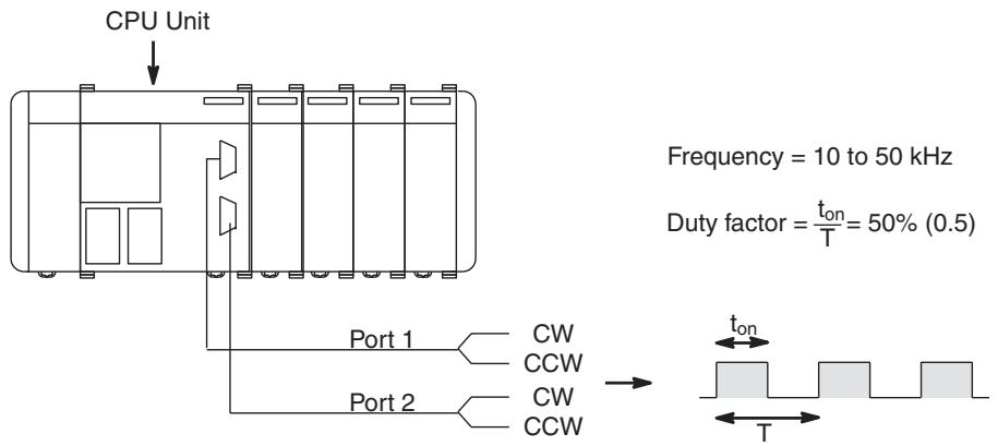
When outputting pulses from ports 1 and 2, the frequency can be changed in steps or by a specified rate, as shown in the following diagram.
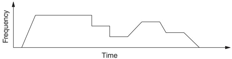
line
| Time | Frequency | |------|---------| | 0 | 0 | | 1 | High | | 2 | High | | 3 | Medium | | 4 | Low | | 5 | Medium | | 6 | High | | 7 | Medium | | 8 | Low | | 9 | Low | | 10 | 0 |Pulse output from ports 1 and 2 can be performed in the following two modes:
- Continuous Mode: Pulse output continues until it is stopped by either a SPED(64) instruction or an INI(61) instruction.
- Independent Mode: Pulse output stops automatically when a specified number of pulses has been output. Output can also be stopped by a SPED(64) or INI(61) instruction.
Note Use INI(61) when pulse output has to be stopped immediately, as for an emergency stop, etc. Pulse output will not stop even if a SPED(64), PLS2(—), or ACC(—) signal turns input OFF.
Only stop pulse output when it is actually being output. Confirm the status of pulse output using the Pulse Output In Progress Flag (AR0515/AR0615).
The following table shows the types of frequency changes that can be made with combinations of PULS(65), SPED(64), INI(61), PLS2(—), and ACC(—).
| Frequency change | Instruction | Operand settings | Page | |
 | Start pulse output at the specified frequency. Execute PULS(65) followed by SPED(64). | PULS(65) | CW/CCW (Number of pulses) | 111 |
| SPED(64) | Port Continuous/Inde-pendent Frequency | |||
 | Change frequency by steps during pulse out-put. | SPED(64) | Port Continuous/Inde-pendent Frequency | |
 | Stop pulse output with an instruction. Execute SPED(64) or INI(61). | SPED(64) | Port Frequency= 0 | 113 |
| INI(61) | Set control data to stop pulse output. | |||
 | Outputs a specified number of pulses. The pulse output accelerates to the target fre-quency at a specified rate, and decelerates to a stop at the same rate. | PLS2(—) | Port CW/CCWAcceleration/Decel-eration rateTarget frequency Number of pulses | 114 |
 | Outputs a specified number of pulses. The pulse output accelerates to the target fre-quency at a specified rate, and decelerates to a stop at another specified rate.ACC(—) instruction mode 0: Acceleration + Independent ModeExecute PULS(65) followed by ACC(—). | PULS(65) | CW/CCW Number of pulses Deceleration point | 115 |
| ACC(—)(Mode 0) | PortAcceleration rate Target frequency 1 Deceleration rate Target frequency 2 | |||
 | Accelerates pulse output from the current frequency to the target frequency at a speci-fied rate.Pulse output will continue.Execute PULS(65) followed by ACC(—).ACC(—) instruction mode 1: Acceleration + Continuous Mode | PULS(65) | CW/CCW | 115 |
| ACC(—)(Mode 1) | PortAcceleration rate Target frequency | |||
 | Decelerates pulse output from the current frequency to the target frequency at a speci-fied rate.Pulse output will stop when the specified number of pulses have been output.Execute PULS(65) followed by ACC(—).ACC(—) instruction mode 2: Deceleration + Independent Mode | PULS(65) | CW/CCW Number of pulses | 116 |
| ACC(—)(Mode 2) | Port Deceleration rate Target frequency | |||
 | Decelerates pulse output from the current frequency to the target frequency at a speci-fied rate.Pulse output will continue.Execute PULS(65) and then ACC(—).ACC(—) instruction mode 3: Deceleration + Continuous Mode | PULS(65) | CW/CCW | 116 |
| ACC(—)(Mode 3) | Port Deceleration rate Target frequency | |||
Single-Phase Fixed Duty Factor Pulse Outputs
The following flowchart shows the procedure for using PULS(65) and SPED(64) to perform single-phase fixed duty factor pulse outputs without acceleration or deceleration.
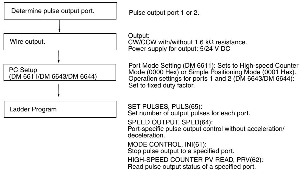
flowchart
graph TD
    A["Determine pulse output port."] --> B["Wire output."]
    B --> C["PC Setup (DM 6611/DM 6643/DM 6644)"]
    C --> D["Ladder Program"]
    E["Pulse output port 1 or 2."] --> F["Output: CW/CCW with/without 1.6 kΩ resistance.<br>Power supply for output: 5/24 V DC"]
    G["Port Mode Setting (DM 6611): Sets to High-speed Counter Mode (0000 Hex) or Simple Positioning Mode (0001 Hex). Operation settings for ports 1 and 2 (DM 6643/DM 6644): Set to fixed duty factor."] --> H["SET PULSES, PULS(65): Set number of output pulses for each port."]
    H --> I["SPEED OUTPUT, SPED(64): Port-specific pulse output control without acceleration/deceleration."]
    I --> J["MODE CONTROL, INI(61): Stop pulse output to a specified port."]
    J --> K["HIGH-SPEED COUNTER PV READ, PRV(62): Read pulse output status of a specified port."]
Single-phase Fixed Duty Factor Pulse Output without Acceleration/Deceleration
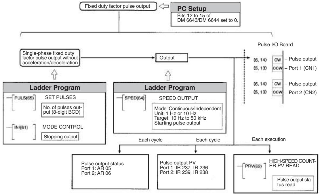
flowchart
graph TD
    A["Fixed duty factor pulse output"] <--> B["PC Setup\nBits 12 to 15 of DM 6643/DM 6644 set to 0."]
    B --> C["Single-phase fixed duty factor pulse output without acceleration/deceleration"]
    C --> D["Output"]
    D --> E["Ladder Program"]
    D --> F["Ladder Program"]
    E --> G["Pulse I/O Board\n(6, 14) CW - Pulse output\n(5, 13) CCW - Port 1 (CN1)\n(6, 14) CW - Pulse output\n(5, 13) CCW - Port 2 (CN2)"]
    F --> H["Pulse output status\nPort 1: AR 05\nPort 2: AR 06"]
    F --> I["Pulse output PV\nPort 1: IR 237, IR 236\nPort 2: IR 239, IR 238"]
    F --> J["HIGH-SPEED COUNT-ER PV READ\nPulse output status read"]
    G --> K["Pulse output status\nPort 1: AR 05\nPort 2: AR 06"]
    H --> L["Pulse output status\nPort 1: AR 05\nPort 2: AR 06"]
    I --> M["Pulse output PV\nPort 1: IR 237, IR 236\nPort 2: IR 239, IR 238"]
    J --> N["Pulse output status\nPort 1: AR 05\nPort 2: AR 06"]
    K --> O["SET PULSES\nNo. of pulses out-put (8-digit BCD)"]
    L --> P["MODE CONTROL\nStopping output"]
    M --> Q["SPEED(64)"]
    N --> R["MODE: Continuous/Independent Unit: 1 Hz or 10 Hz\nTarget: 10 Hz to 50 kHz\nStarting pulse output"]
    O --> S["Pulse output status\nPort 1: AR 05\nPort 2: AR 06"]
    P --> T["Pulse output PV\nPort 1: IR 237, IR 236\nPort 2: IR 239, IR 238"]
Trapezoidal Pulse Output With Same Acceleration/Deceleration
The following flowchart shows the procedure for using PLS2(—) to perform trapezoidal pulse outputs with the same acceleration/deceleration rate.
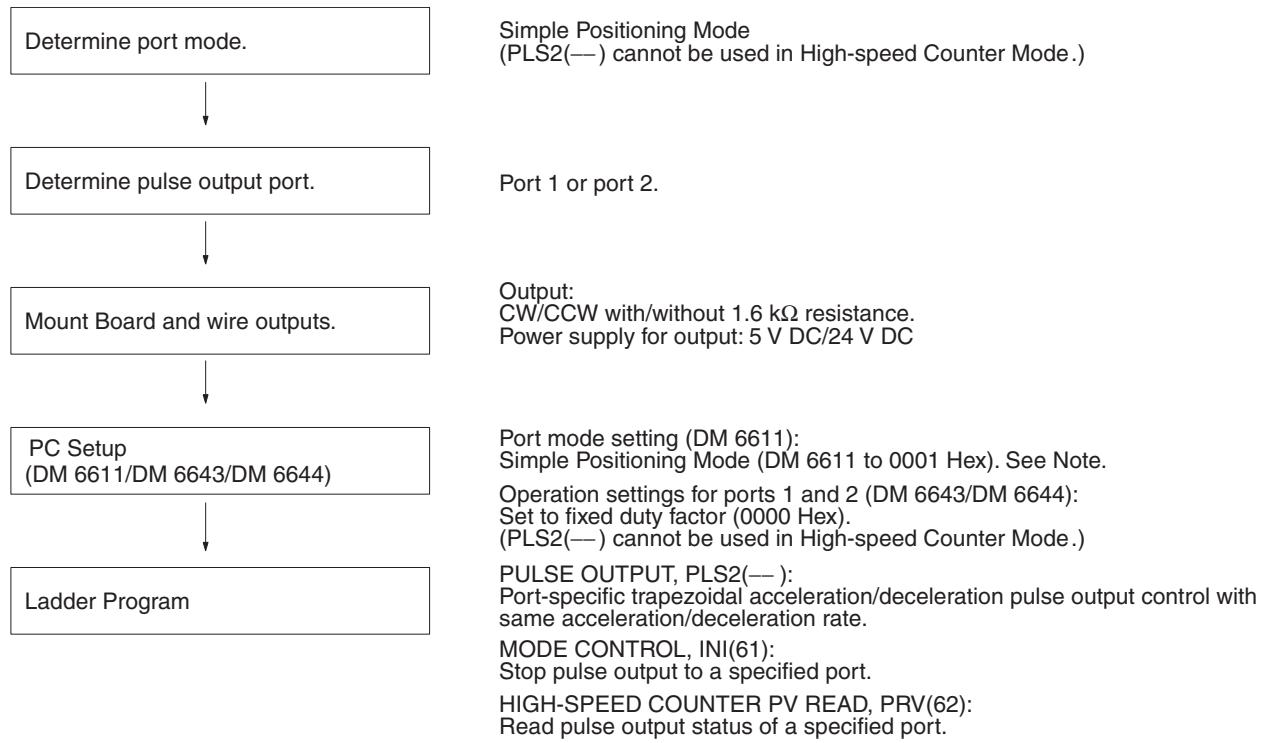
flowchart
graph TD
    A["Determine port mode."] --> B["Determine pulse output port."]
    B --> C["Mount Board and wire outputs."]
    C --> D["PC Setup (DM 6611/DM 6643/DM 6644)"]
    D --> E["Ladder Program"]

    F["Simple Positioning Mode (PLS2(---) cannot be used in High-speed Counter Mode.)"] --> G["Port 1 or port 2."]
    G --> H["Output: CW/CCW with/without 1.6 kΩ resistance.<br>Power supply for output: 5 V DC/24 V DC"]
    H --> I["Port mode setting (DM 6611): Simple Positioning Mode (DM 6611 to 0001 Hex). See Note."]
    I --> J["Operation settings for ports 1 and 2 (DM 6643/DM 6644): Set to fixed duty factor (0000 Hex). (PLS2(---) cannot be used in High-speed Counter Mode.)"]
    J --> K["PULSE OUTPUT, PLS2(---): Port-specific trapezoidal acceleration/deceleration pulse output control with same acceleration/deceleration rate."]
    K --> L["MODE CONTROL, INI(61): Stop pulse output to a specified port."]
    L --> M["HIGH-SPEED COUNTER PV READ, PRV(62): Read pulse output status of a specified port."]
Trapezoidal Acceleration/Deceleration Pulse Outputs
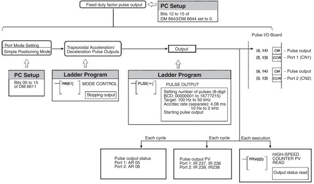
flowchart
graph TD
    A["Fixed duty factor pulse output"] --> B["PC Setup"]
    B --> C["Bits 12 to 15 of DM 6643/DM 6644 set to 0."]
    B --> D["Port Mode Setting\nSimple Positioning Mode"]
    D --> E["Trapezoidal Acceleration/Deceleration Pulse Outputs"]
    E --> F["Output"]
    F --> G["Pulse I/O Board"]
    G --> H["(6, 14)\nCW\n(5, 13)"]
    G --> I["(6, 14)\nCW\n(5, 13)"]
    G --> J["Pulse output\nPort 1 (CN1)"]
    G --> K["Pulse output\nPort 2 (CN2)"]
    L["PC Setup\nBits 00 to 15 of DM 6611"] --> M["Ladder Program"]
    M --> N["MODE CONTROL\nStopping output"]
    O["Ladder Program\n[PLS2(-)"] PULSE OUTPUT\nSetting number of pulses (8-digit BCD: 00000001 to 16777215)\nTarget: 100 Hz to 50 kHz\nAcc/dec rate (separate): 4.08 ms\n10 Hz to 2 kHz\nStarting pulse output]
    P["Pulse output status\nPort 1: AR 05\nPort 2: AR 06"] --> Q["Each cycle"]
    R["Pulse output PV\nPort 1: IR 237, IR 236\nPort 2: IR 239, IR238"] --> S["Each cycle"]
    T["PRV(62)"] HIGH-SPEED COUNTER PV READ\nOutput status read] --> U["Each execution"]
Trapezoidal Pulse Output With Different Acceleration/Deceleration
The following flowchart shows the procedure for using PULS(65) and ACC(—) to perform trapezoidal pulse outputs with different acceleration/ deceleration rates.
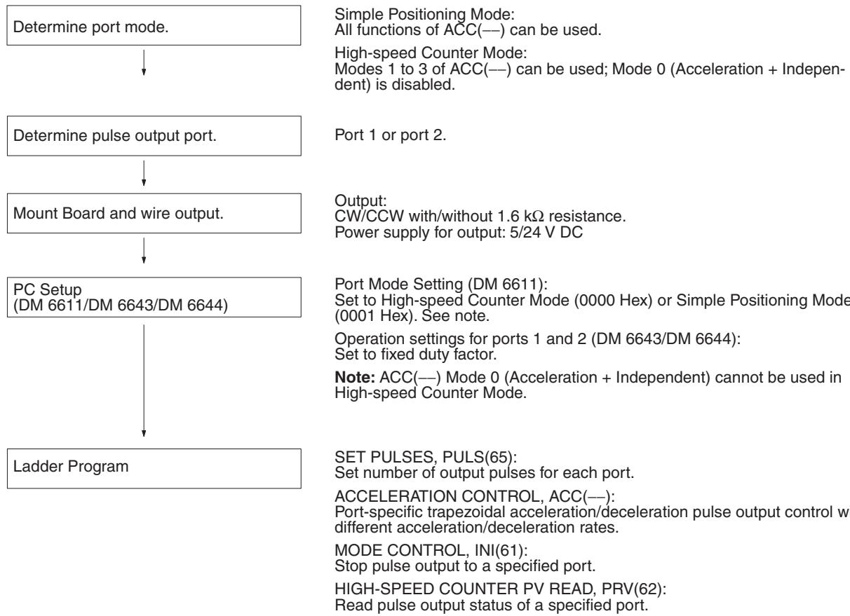
flowchart
graph TD
    A["Determine port mode."] --> B["Determine pulse output port."]
    B --> C["Mount Board and wire output."]
    C --> D["PC Setup (DM 6611/DM 6643/DM 6644)"]
    D --> E["Ladder Program"]
    F["Simple Positioning Mode: All functions of ACC(--) can be used."] --> G["High-speed Counter Mode: Modes 1 to 3 of ACC(--) can be used; Mode 0 (Acceleration + Independent) is disabled."]
    G --> H["Port 1 or port 2."]
    I["Output: CW/CCW with/without 1.6 kΩ resistance. Power supply for output: 5/24 V DC"] --> J["Port Mode Setting (DM 6611): Set to High-speed Counter Mode (0000 Hex) or Simple Positioning Mode (0001 Hex). See note. Operation settings for ports 1 and 2 (DM 6643/DM 6644): Set to fixed duty factor. Note: ACC(--) Mode 0 (Acceleration + Independent) cannot be used in High-speed Counter Mode."]
    J --> K["SET PULSES, PULS(65): Set number of output pulses for each port. ACCELERATION CONTROL, ACC(---): Port-specific trapezoidal acceleration/deceleration pulse output control with different acceleration/deceleration rates. MODE CONTROL, INI(61): Stop pulse output to a specified port. HIGH-SPEED COUNTER PV READ, PRV(62): Read pulse output status of a specified port."]
Trapezoidal Acceleration/Deceleration Pulse Outputs
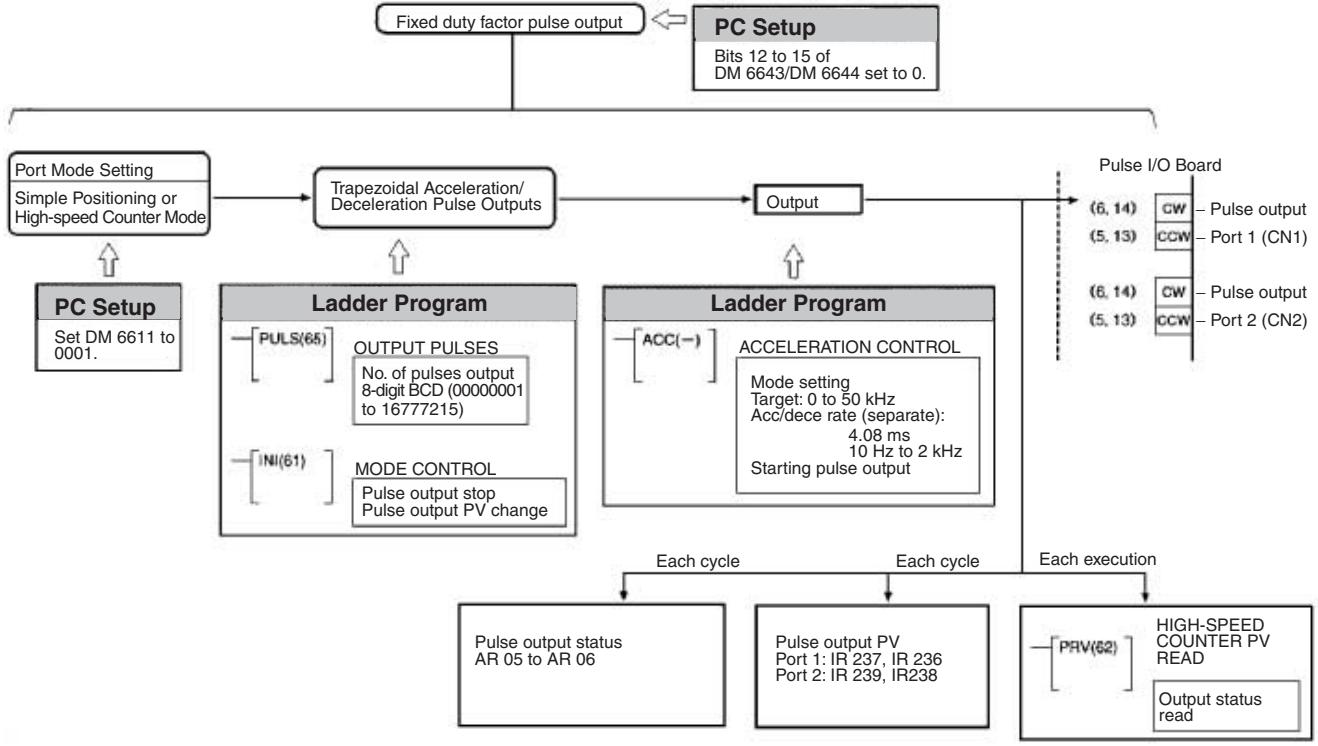
flowchart
graph TD
    A["Fixed duty factor pulse output"] --> B["PC Setup"]
    B --> C["Bits 12 to 15 of DM 6643/DM 6644 set to 0."]
    C --> D["Trapezoidal Acceleration/Deceleration Pulse Outputs"]
    D --> E["Output"]
    E --> F["Pulse I/O Board"]
    F --> G["(6, 14)"]
    G --> H["CW"]
    G --> I["(5, 13)"]
    G --> J["CCW"]
    F --> K["Pulse output"]
    F --> L["Port 1 (CN1)"]
    F --> M["Pulse output"]
    F --> N["Port 2 (CN2)"]
    D --> O["Port Mode Setting"]
    O --> P["Simple Positioning or High-speed Counter Mode"]
    D --> Q["PC Setup"]
    Q --> R["Set DM 6611 to 0001."]
    D --> S["Ladder Program"]
    S --> T["PULS(65)"]
    T --> U["OUTPUT PULSES"]
    U --> V["No. of pulses output 8-digit BCD (00000001 to 16777215)"]
    S --> W["INI(61)"]
    W --> X["MODE CONTROL"]
    X --> Y["Pulse output stop"]
    X --> Z["Pulse output PV change"]
    E --> AA["ACCELERATION CONTROL"]
    AA --> AB["Mode setting"]
    AB --> AC["Target: 0 to 50 kHz"]
    AB --> AD["Acc/dece rate (separate): 4.08 ms, 10 Hz to 2 kHz"]
    AA --> AE["Starting pulse output"]
    F --> AF["Pulse output status AR 05 to AR 06"]
    F --> AG["Pulse output PV Port 1: IR 237, IR 236, Port 2: IR 239, IR238"]
    F --> AH["PRV(62)"]
    AH --> AI["HIGH-SPEED COUNTER PV READ"]
    F --> AJ["Output status read"]
PC Setup Settings
Before outputting pulses from port 1 or 2, switch the PC to PROGRAM mode and enter the following settings in the PC Setup.
Port Mode Setting (DM 6611)
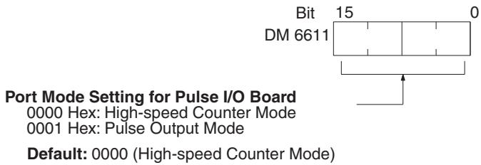
The instructions that can be used are limited by the Port Mode setting for ports 1 and 2 of the Pulse I/O Board. The Port Mode is specified in the PC Setup (DM 6611).
Port Mode Setting and Instructions
The following tables show the port mode settings and the instructions that can be used with various pulse outputs.
Pulse Output without Trapezoidal Acceleration/Deceleration
All instructions can be used regardless of the port mode setting.
| Instruction | PULS(65) | SPED(64) | INI(61) | PRV(62) |
| Function | Sets number of pulses | Sets frequency | Stops pulse output | Reads pulse output status |
| (Used in combination.) | ||||
| High-speed Counter Mode | Enabled | |||
| Simple Positioning Mode | Enabled | |||
Pulse Output with Trapezoidal Acceleration/Deceleration and the Same Acceleration/Deceleration Rate
PLS2(—) (PULSE OUTPUT) cannot be used in High-speed Counter Mode. It is not possible to perform trapezoidal acceleration/deceleration pulse output using the same acceleration/deceleration rates.
| Instruction | PLS2(—) | INI(61) | PRV(62) |
| Function | Sets number of pulses | Stops pulse output | Reads pulse output status |
| High-speed Counter Mode | Disabled | Enabled | |
| Simple Positioning Mode | Enabled | ||
Pulse Output with Trapezoidal Acceleration/Deceleration and Separate Acceleration/Deceleration Rates
The only limitation that exists is that ACC(—) (ACCELERATION CONTROL) in Mode 0 (Acceleration + Independent) cannot be used in High-speed Counter Mode.
| Instruction | PULS(65) | ACC(—) | INI(61) | PRV(62) |
| Function | Sets number of pulses | Acceleration/ Deceleration rates (separate settings)Sets frequencyStarts pulse output | Stops pulse output | Reads pulse output status |
| (Used in combination.) | ||||
| High-speed Counter Mode | Enabled | Mode 0 (Acc.+ Independent): DisabledMode 3: Enabled | Enabled | |
| Simple Positioning Mode | Enabled | |||
The setting in DM 6611 is read only when the CQM1H is started. If this setting is changed, the PC must be turned OFF and ON again to enable the new value.
Operation Settings for Ports 1 and 2 (DM 6643 and DM 6644)
The diagram below shows how port 1 (DM 6643) and port 2 (DM 6644) are set to perform fixed duty factor pulse output, which is the default pulse output format. The settings for ports 1 and 2 can differ.
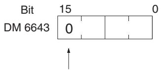
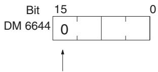
Port 1 Pulse Type
0: Fixed duty factor pulse output Set to fixed duty factor when performing standard pulse output. 1: Variable duty factor pulse output
Default: 0 (Fixed duty factor pulse output)
Port 2 Pulse Type
0: Fixed duty factor pulse output Set to fixed duty factor when performing standard pulse output. 1: Variable duty factor pulse output
Default: 0 (Fixed duty factor pulse output)
Examples
Variable duty factor pulses cannot be output from a port if it has been set to perform standard pulse output.
The following examples show programs that controls pulse output from ports 1 and 2. Before running the programs, check that the settings in the PC Setup are as follows:
DM 6611: 0001 (Simple Positioning Mode)
DM 6643: 0000 (Fixed duty factor pulse output from port 1)
DM 6644: 0000 (Fixed duty factor pulse output from port 2)
Example 1: Starting Pulse Output with PULS(65) and SPED (64)
Starting Pulse Output at Specified Frequency
The following example shows PULS(65) and SPED(64) used to control a pulse output from port 1. The number of pulses specified in PULS(65)(10,000) are output as the frequency is changed by executions of SPED(64) with different frequency settings.

flowchart
graph TD
    A["05000"] --> B["@PULS(65)"]
    B --> C["001"]
    B --> D["000"]
    B --> E["DM 0000"]
    A --> F["@SPED(64)"]
    F --> G["001"]
    F --> H["000"]
    F --> I["#0100"]
    A --> J["00000"]
    J --> K["@SPED(64)"]
    K --> L["001"]
    K --> M["000"]
    K --> N["#0150"]
    A --> O["00001"]
    O --> P["@SPED(64)"]
    P --> Q["001"]
    P --> R["000"]
    P --> S["#0100"]
    A --> T["00002"]
    T --> U["@SPED(64)"]
    U --> V["001"]
    U --> W["000"]
    U --> X["#0050"]
When IR 05000 turns ON, PULS(65) sets port 1 for 10,000 CW pulses.
DM 0000: 0000
DM 0001: 0001
Starts pulse output from port 1 at 1,000 Hz in Independent Mode.
When IR 00000 turns ON, the pulse frequency from port 1 is changed to 1,500 Hz.
When IR 00001 turns ON, the pulse frequency from port 1 is changed to 1,000 Hz.
When IR 00002 turns ON, the pulse frequency from port 1 is changed to 500 Hz.
The following diagram shows the frequency of pulse outputs from port 1 as the program is executed.
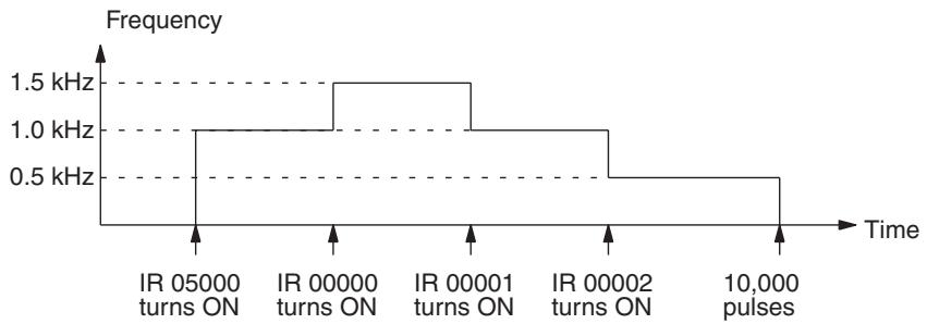
line
| Time | Frequency | | ----------------- | --------- | | IR 05000 turns ON | 1.0 kHz | | IR 00000 turns ON | 1.5 kHz | | IR 00001 turns ON | 1.0 kHz | | IR 00002 turns ON | 0.5 kHz | | 10,000 pulses | 0.5 kHz |Caution Be sure that the pulse frequency is within the motor's self-starting frequency range when starting and stopping the motor.
Note Speed control timing will be accurate when frequency changes are performed as input interrupt processes.
Example 2: Stopping Pulse Output with SPED(64)
The following example shows PULS(65) and SPED(64) used to control a pulse output from port 1. The frequency is changed by executions of SPED(64) with different frequency settings and finally stopped with a frequency setting of 0.
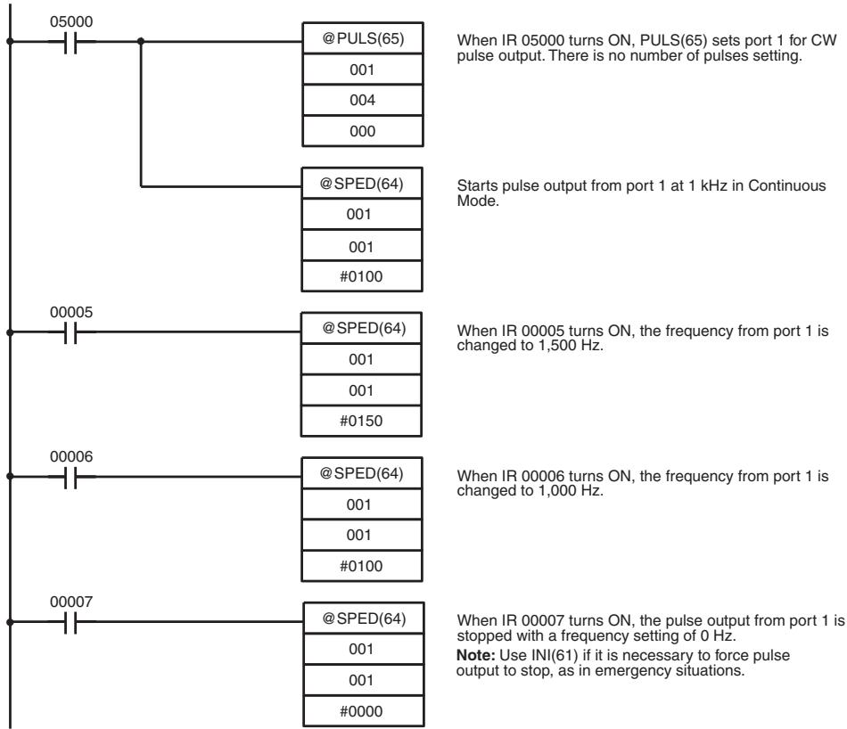
flowchart
graph TD
    A["05000"] --> B["@PULS(65)"]
    B --> C["When IR 05000 turns ON, PULS(65) sets port 1 for CW pulse output. There is no number of pulses setting."]
    B --> D["001"]
    B --> E["004"]
    B --> F["000"]
    A --> G["@SPED(64)"]
    G --> H["Starts pulse output from port 1 at 1 kHz in Continuous Mode."]
    G --> I["001"]
    G --> J["001"]
    G --> K["#0100"]
    A --> L["@SPED(64)"]
    L --> M["When IR 00005 turns ON, the frequency from port 1 is changed to 1,500 Hz."]
    L --> N["001"]
    L --> O["001"]
    L --> P["#0150"]
    A --> Q["@SPED(64)"]
    Q --> R["When IR 00006 turns ON, the frequency from port 1 is changed to 1,000 Hz."]
    Q --> S["001"]
    Q --> T["001"]
    Q --> U["#0100"]
    A --> V["@SPED(64)"]
    V --> W["When IR 00007 turns ON, the pulse output from port 1 is stopped with a frequency setting of 0 Hz. Note: Use INI(61) if it is necessary to force pulse output to stop, as in emergency situations."]
    A --> X["@SPED(64)"]
    X --> Y["When IR 00007 turns ON, the pulse output from port 1 is stopped with a frequency setting of 0 Hz. Note: Use INI(61) if it is necessary to force pulse output to stop, as in emergency situations."]
The following diagram shows the frequency of pulse outputs from port 1 as the program is executed.
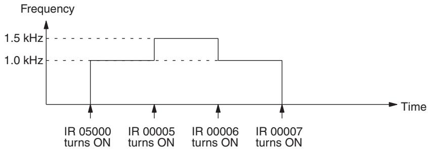
line
| Time | Frequency | | ---------- | --------- | | IR 05000 | 1.0 kHz | | IR 00005 | 1.5 kHz | | IR 00006 | 1.5 kHz | | IR 00007 | 1.0 kHz |
Be sure that the pulse frequency is within the motor's self-starting frequency range when starting and stopping the motor.
Example 3: Using PLS(—) to Accelerate/Decelerate the Frequency at the Same Rate
The following example shows PLS2(—) used to output 100,000 CW pulses from port 1. The frequency is accelerated to 10 kHz at approximately 500 Hz/4 ms and decelerated at the same rate.
Five seconds after the CW pulses have been output, another PLS2(—) instruction outputs 100,000 CCW pulses with the same settings.
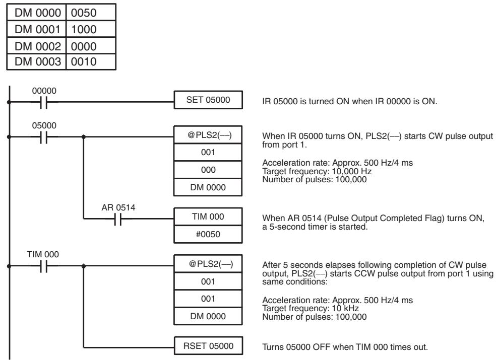
| DM 0000 | 0050 |
| DM 0001 | 1000 |
| DM 0002 | 0000 |
| DM 0003 | 0010 |
IR 05000 is turned ON when IR 00000 is ON.
When IR 05000 turns ON, PLS2(—) starts CW pulse output from port 1.
Acceleration rate: Approx. 500 Hz/4 ms
Target frequency: 10,000 Hz
Number of pulses: 100,000
When AR 0514 (Pulse Output Completed Flag) turns ON, a 5-second timer is started.
After 5 seconds elapses following completion of CW pulse output, PLS2(—) starts CCW pulse output from port 1 using same conditions:
Acceleration rate: Approx. 500 Hz/4 ms
Target frequency: 10 kHz
Number of pulses: 100,000
Turns 05000 OFF when TIM 000 times out.
The following diagram shows the frequency of pulse outputs from port 1 as the program is executed.
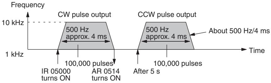
line
| Pulse Type | Frequency Range | Approx. Time (ms) | | ---------------- | ----------------------- | ----------------- | | CW pulse output | 500 Hz approx. 4 ms | 4 | | CW pulse output | IR 05000 turns ON | - | | CW pulse output | AR 0514 turns ON | - | | CCW pulse output | 500 Hz approx. 4 ms | About 500 Hz/4 ms | | CCW pulse output | After 5 s | - | | CCW pulse output | 100,000 pulses | - |Example 4: Using
ACC(—) to Accelerate/
Decelerate the Frequency at Different Rates
The following example shows Mode 0 of ACC(—) used to output 10,000 CW pulses from port 1. The frequency is accelerated to 10 kHz at approximately 1 kHz/4 ms and decelerated to 1 kHz at approximately 250 Hz/4 ms. Deceleration begins after 9,100 pulses have been output.
When IR 00000 turns ON, PULS(65) sets port 1 for CW pulse output. The total number of pulses is set to 10,000 and the deceleration point is set to 9,100 pulses.
Starts CW pulse output from port 1.
Acceleration rate: Approx. 1000 Hz/4 ms
Target frequency after acceleration: 10,000 Hz
Deceleration rate: Approx. 250 Hz/4 ms
Target frequency after deceleration: 1 kHz
Following deceleration, pulse output starts at target frequency of approx. 500 Hz/4 ms.
The following diagram shows the frequency of pulse outputs from port 1 as the program is executed.

line
| Time | Frequency | | ----------------- | --------- | | IR 00000 turns ON | 1 kHz | | 9,100 pulses | 1 kHz | | 10,000 pulses | 1 kHz |Example 5: Using
ACC(—) to Accelerate the
Frequency at a Specified Rate
The following example shows Mode 1 of ACC(—) used to increase the frequency of a pulse output from port 1. The frequency is accelerated from 1 kHz to 20 kHz at approximately 500 Hz/4 ms.
| DM 0000 | 0050 |
| DM 0001 | 2000 |
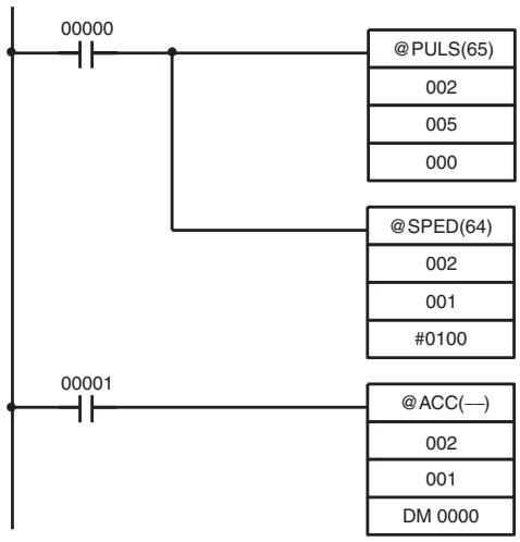
flowchart
graph TD
    A["00000"] --> B["@PULS(65)"]
    B --> C["002"]
    B --> D["005"]
    B --> E["000"]
    F["00001"] --> G["@ACC(-)"]
    G --> H["002"]
    G --> I["001"]
    G --> J["DM 0000"]
    B --> K["@SPED(64)"]
    K --> L["002"]
    K --> M["001"]
    K --> N["#0100"]
When IR 00000 turns ON, PULS(65) sets port 2 for CCW pulse output. The number of pulses is not set.
Starts 1,000 Hz (1 kHz) pulse output from port 2 in Continuous Mode.
When IR 00001 turns ON, ACC(—) begins accelerating the port 2 pulse output at about 500 Hz/4 ms until it reaches the target frequency of 20,000 Hz.
The following diagram shows the frequency of pulse outputs from port 2 as the program is executed.
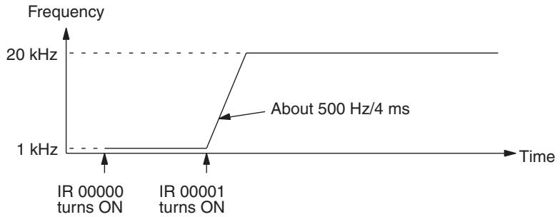
line
| Time | Frequency | | ----------------- | --------- | | IR 00000 turns ON | 1 kHz | | IR 00001 turns ON | 20 kHz | | About 500 Hz/4 ms | 20 kHz |Example 6: Using ACC(—) to Decelerate the Frequency at a Specified Rate and Stop Output
The following example shows Mode 2 of ACC(—) used decrease the frequency of a pulse output from port 1. The 2-kHz pulse output is already in progress in independent mode and stops automatically when the number of pulses is reached.
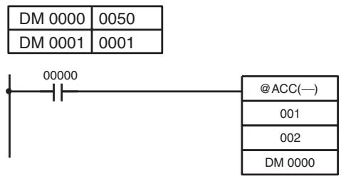
flowchart
graph TD
    A["DM 0000"] --> B["0050"]
    C["DM 0001"] --> D["0001"]
    E["00000"] --> F["@ACC(—)"]
    G["001"] --> F
    H["002"] --> F
    I["DM 0000"] --> F
When IR 00000 turns ON, ACC(—) begins decelerating the port 1 pulse frequency at about 500 Hz/4 ms until it reaches the target frequency of 10 Hz. Pulse output stops when the specified number of pulses is reached.
The following diagram shows the frequency of pulse outputs from port 1 as the program is executed.

line
| Time | Frequency | | ---- | --------- | | IR 00000 turns ON | 2 kHz | | Specified number of pulses output | 1 kHz | | Specific pulse output | About 500 Hz/4 ms |Note The pulse output can be stopped by executing ACC(—) Mode 2 with a target frequency of 0. However, since the pulse output cannot be stopped at the correct number of pulses, this method should not be used except for emergency stops.
Example 7: Using ACC(—) to Decelerate the Frequency at a Specified Rate
The following example shows Mode 3 of ACC(—) used to decrease the frequency of a pulse output from port 1. The 20-kHz pulse output is already in progress in Continuous Mode.
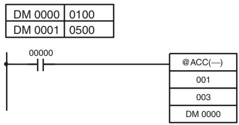
flowchart
graph TD
    A["DM 0000 0100"] --> B["00000"]
    C["DM 0001 0500"] --> B
    B --> D["@ACC(—)"]
    D --> E["001"]
    D --> F["003"]
    D --> G["DM 0000"]
When IR 00000 turns ON, ACC(—) begins decelerating the port 1 pulse output at about 1,000 Hz/4 ms until it reaches the target frequency of 5,000 Hz.
The following diagram shows the frequency of pulse outputs from port 1 as the program is executed.
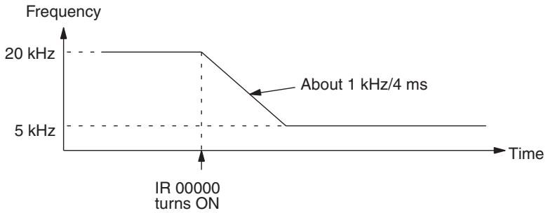
line
| Time | Frequency | | ----------------- | --------- | | IR 00000 turns ON | 5 kHz | | Above 1 kHz/4 ms | 20 kHz |2-2-10 Variable Duty Factor Pulse Outputs
The following is the procedure for outputting pulses with varying duty factors (i.e., the ratio of the pulse ON time and the pulse cycle) from ports 1 and/or 2. This function can be used for various kinds of control outputs, such as light intensity output or speed control output to an inverter.
Outline
Variable duty factor pulse outputs from ports 1 and/or 2 are executed as shown in the diagram below. Ports 1 and 2 can be used at the same time.
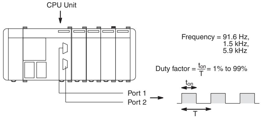
Variable Duty Factor Pulse Outputs Using PWM(—)
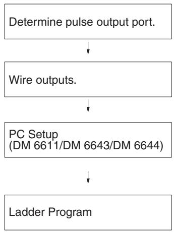
flowchart
graph TD
    A["Determine pulse output port."] --> B["Wire outputs."]
    B --> C["PC Setup (DM 6611/DM 6643/DM 6644)"]
    C --> D["Ladder Program"]
Port 1 or port 2.
Output: PWM(—) with/without 1.6 kΩ resistance. Power supply for output: 5/24 V DC
Port Mode Setting (DM 6611): High-speed Counter Mode (0000 Hex) or Simple Positioning Mode (0001 Hex) Operation settings for ports 1 and 2 (DM 6643/DM 6644): Set to variable duty factor (1000 Hex).
PULSE WITH VARIABLE DUTY FACTOR, PWM(—): Set frequency and duty factor.
MODE CONTROL, INI(61): Stop pulse output to a specified port.
HIGH-SPEED COUNTER PV READ, PRV(62): Read pulse output status of a specified port.
Variable Duty Factor Pulse Outputs
flowchart
graph TD
    A["Variable duty factor pulse output"] --> B["PC Setup"]
    B --> C["Pulse I/O Board"]
    C --> D["Ladder Program"]
    D --> E["Each cycle"]
    D --> F["Each execution"]
    E --> G["Pulse output status\nPort 1: AR 05\nPort 2: AR 06"]
    F --> H["HIGH-SPEED COUNTER PV READ\nPulse output status read"]
    G --> I["Pulse output status\nPort 1: AR 05\nPort 2: AR 06"]
    H --> J["Pulse output status\nPort 1: AR 05\nPort 2: AR 06"]
    I --> K["Pulse output status\nPort 1: AR 05\nPort 2: AR 06"]
    J --> L["Pulse output status\nPort 1: AR 05\nPort 2: AR 06"]
    K --> M["Pulse output status\nPort 1: AR 05\nPort 2: AR 06"]
    L --> N["Pulse output status\nPort 1: AR 05\nPort 2: AR 06"]
    M --> O["Pulse output status\nPort 1: AR 05\nPort 2: AR 06"]
    N --> P["Pulse output status\nPort 1: AR 05\nPort 2: AR 06"]
    O --> Q["Pulse output status\nPort 1: AR 05\nPort 2: AR 06"]
    P --> R["Pulse output status\nPort 1: AR 05\nPort 2: AR 06"]
    Q --> S["Pulse output status\nPort 1: AR 05\nPort 2: AR 06"]
    R --> T["Pulse output status\nPort 1: AR 05\nPort 2: AR 06"]
    S --> U["Pulse output status\nPort 1: AR 05\nPort 2: AR 06"]
    T --> V["Pulse output status\nPort 1: AR 05\nPort 2: AR 06"]
    U --> W["Pulse output status\nPort 1: AR 05\nPort 2: AR 06"]
    V --> X["Pulse output status\nPort 1: AR 05\nPort 2: AR 06"]
    W --> Y["Pulse output status\nPort 1: AR 05\nPort 2: AR 06"]
    X --> Z["Pulse output status\nPort 1: AR 05\nPort 2: AR 06"]
    Y --> AA["Pulse output status\nPort 1: AR 05\nPort 2: AR 06"]
    Z --> AB["Pulse output status\nPort 1: AR 05\nPort 2: AR 06"]
    AA --> AC["Pulse output status\nPort 1: AR 05\nPort 2: AR 06"]
    AB --> AD["Pulse output status\nPort 1: AR 05\nPort 2: AR 06"]
    AC --> AE["Pulse output status\nPort 1: AR 05\nPort 2: AR 06"]
    AD --> AF["Pulse output status\nPort 1: AR 05\nPort 2: AR 06"]
    AE --> AG["Pulse output status\nPort 1: AR 05\nPort 2: AR 06"]
    AF --> AH["Pulse output status\nPort 1: AR 05\nPort 2: AR 06"]
    AG --> AI["Pulse output status\nPort 1: AR 05\nPort 2: AR 06"]
    AH --> AJ["Pulse output status\nPort 1: AR 05\nPort 2: AR 06"]
    AI --> AK["Pulse output status\nPort 1: AR 05\nPort 2: AR 06"]
    AJ --> AL["Pulse output status\nPort 1: AR 05\nPort 2: AR 06"]
    AK --> AM["Pulse output status\nPort 1: AR 05\nPort 2: AR 06"]
    AL --> AN["Pulse output status\nPort 1: AR 05\nPort 2: AR 06"]
    AM --> AO["Pulse output status\nPort 1: AR 05\nPort 2: AR 06"]
    AN --> AP["Pulse output status\nPort 1: AR 05\nPort 2: AR 06"]
    AP --> AQ["Pulse output status\nPort 1: AR 05\nPort 2: AR 06"]
    AQ --> AR["Pulse output status\nPort 1: AR 05\nPort 2: AR 06"]
    AR --> AS["Pulse output status\nPort 1: AR 05\nPort 2: AR 06"]
    AS --> AT["Pulse output status\nPort 1: AR 05\nPort 2: AR 06"]
    AT --> AU["Pulse output status\nPort 1: AR 05\nPort 2: AR 06"]
    AU --> AV["Pulse output status\nPort 1: AR 05\nPort 2: AR 06"]
    AV --> AW["Pulse output status\nPort 1: AR 05\nPort 2: AR 06"]
    AW --> AX["Pulse output status\nPort 1: AR 05\nPort 2: AR 06"]
    AX --> AY["Pulse output status\nPort 1: AR 05\nPort 2: AR 06"]
    AY --> AZ["Pulse output status\nPort 1: AR 05\nPort 2: AR 06"]
    AZ --> BA["Pulse output status\nPort 1: AR 05\nPort 2: AR 06"]
    BA --> BB["Pulse output status\nPort 1: AR 05\nPort 2: AR 06"]
    BB --> BC["Pulse output status\nPort 1: AR 05\nPort 2: AR 06"]
    BC --> BD["Pulse output status\nPort 1: AR 05\nPort 2: AR 06"]
    BD --> BE["Pulse output status\nPort 1: AR 05\nPort 2: AR 06"]
    BE --> BF["Pulse output status\nPort 1: AR 05\nPort 2: AR 06"]
    BF --> BG["Pulse output status\nPort 1: AR 05\nPort 2: AR 06"]
    BG --> BH["Pulse output status\nPort 1: AR 05\nPort 2: AR 06"]
    BH --> BI["Pulse output status\nPort 1: AR 05\nPort.2:CW"]
    BI --> BJ["Port.1 pulse output (CN1)"]
    BJ --> BK[" port.1 pulse output (CN1) "]
    BK --> BL[" port.1 pulse output (CN1) "]
    BL --> BM[" port.2 pulse output (CN2) "]
    BM --> BN[" port.2 pulse output (CN2) "]
PC Setup Settings
Before outputting variable duty factor pulses from port 1 or 2, switch the PC to PROGRAM Mode and make the following settings in the PC Setup.
Operation Settings of Ports 1 and 2
Make the following settings to set port 1 (DM 6643) or port 2 (DM 6644) to variable duty factor pulse output mode. Ports 1 and 2 can be set separately.
Port 1 Pulse Type
0: Fixed duty factor pulse output
1: Variable duty factor pulse output
Default: 0
(Fixed duty factor pulse output)
Port 2 Pulse Type
0: Fixed duty factor pulse output
1: Variable duty factor pulse output
Default: 0
(Fixed duty factor pulse output)
Note
- When a port is set to variable duty factor pulse output, it cannot output fixed duty factor pulses.
- When using variable duty factor pulse output, all instructions can be used, regardless of the Port Mode.
| Instruction | PWM(—) | INI(61) | PRV(62) |
| Function | Frequency settingDuty factor settingPulse output start | Pulse output stop | Pulse output status read |
| High-speed Counter Mode | Enabled | ||
| Simple Positioning Mode | Enabled | ||
Starting the Pulse Output
PWM(—) is used to specify the port number, the pulse frequency, and the duty factor, and to start pulse output.
P: Port
001: Port 1
002: Port 2
F: Output frequency
000 = 5.9 kHz
001 = 1.5 kHz
002 = 91.6 Hz
D: Duty factor
Specify either a 4-digit BCD constant or a word address where the value of D is stored as a 4-digit BCD representing a percentage value. The setting must be between 0001 and 0099 (i.e., 1% to 99%).
Pulse output will start using the settings specified by PWM(—), and will continue with those settings until PWM(—) is executed again with different settings, or until INI(61) is executed to stop pulse outputs from the specified port.
Stopping the Pulse Output
The pulse output from a port can be stopped by executing INI(61) with C=003. Specify port 1 or 2 (P=001 or 002).
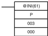
P: Port
001: Port 1
002: Port 2
Example: Using PWM(—)
The following example shows PWM(—) used to start a 1.5 kHz pulse output from port 1 and then change the duty factor from 50% to 25%. The pulse output is then stopped with INI(61). Before running the program, check that the settings in the PC Setup are as follows:
DM 6643: 1000 (variable duty factor pulse setting for port 1).
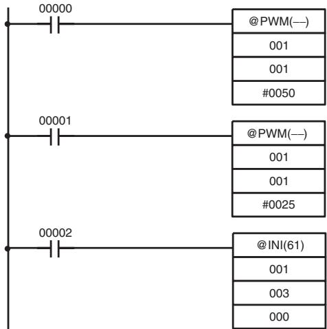
flowchart
graph TD
    A["00000"] --> B["@PWM(—)"]
    B --> C["001"]
    B --> D["001"]
    B --> E["#0050"]
    F["00001"] --> G["@PWM(—)"]
    G --> H["001"]
    G --> I["001"]
    G --> J["#0025"]
    K["00002"] --> L["@INI(61)"]
    L --> M["001"]
    L --> N["003"]
    L --> O["000"]
When IR 00000 turns ON, a 1.5 kHz signal is output from port 1 with a duty factor of 50%.
When IR 00001 turns ON, the duty factor is changed to 25%.
When IR 00002 turns ON, INI(61) stops the pulse output from port 1.
The following diagram shows the duty factor of the pulse output from port 1 as the program is executed.
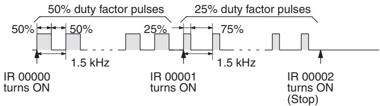
other
| Pulse ID | Duration | Percentage | | -------------- | -------- | ---------- | | IR 00000 | turns ON | 50% | | IR 00001 | turns ON | 25% | | IR 00002 | stops ON | 75% |2-2-11 Determining the Status of Ports 1 and 2
The status of pulse outputs (fixed or variable duty factor pulses) of ports 1 and 2 can be determined either by reading the status of the relevant flags in the SR and AR areas or by executing PRV(62).
Reading Flag Status
The memory words associated with the status of pulse outputs from ports 1 and 2 are shown in the following tables. The pulse output status can be determined by reading the contents of the words and flags shown in these words.
- Inner Board Error Codes
| Word | Bits | Slot | Function |
| AR 04 | 08 to 15 | Slot 2 | Error codes are stored as two-digit hexadecimal:00 Hex: Normal01 and 02 Hex: Hardware error02 Hex: PC Setup error03 Hex: PC stopped during pulse output |
• Operation Status Indicators
| Word | Bit | Name | Function | |
| Port 1 | Port 2 | |||
| AR 05 | AR 06 | 12 | Deceleration Flag | Indicates the passage through a deceleration point when deceleration is specified.0: Not specified1: Specified |
| 13 | Number of Pulses Flag | Stores whether or not the number of pulses have been specified.0: Not specified1: Specified | ||
| 14 | Pulse Output Completed Flag | Indicates the completion status of the pulse output.0: Not completed1: Completed | ||
| 15 | Pulse Output Status Flag | Indicates the operation status of the pulse output.0: Pulse output stopped1: Pulse output in progress | ||
Using PRV(62)
The status of pulse outputs can be determined by using PRV(62). Specify port 1 or 2 (P=001 to 002) and the destination word D.
| @PRV(62) |
| P |
| 001 |
| D |
P: Port specifier
C: 001
D: First destination word
The bits comprising the pulse output status information stored in D have the following meanings:
| Bit | Function | Description |
| 04 | Deceleration Flag | Indicates deceleration.(0: Not decelerating; 1: Decelerating) |
| 05 | Number of Pulses Flag | Indicates whether the total number of pulses have been specified. (0: Not specified; 1: Specified.) |
| 06 | Pulse Output Com- pleted Flag | Indicates whether pulse output has been completed.(0: Not completed; 1: Completed.) |
| 07 | Pulse Output Status Flag | Indicates whether pulses are being output.(0: No output; 1: Output in progress.) |
In addition to the above, bits 0 and 1 store information about the status of the high-speed counter. All other bits are 0.
Note When PRV(62) is used to read a port's status, the most recent information will be read regardless of the PC's cycle time.
2-2-12 Precautions When Using Pulse Output Functions
The Pulse I/O Board divides the 500 kHz source clock by an integer value to generate an output pulse frequency. For this reason, the frequency setting and the frequency actually produced may differ. Refer to the following formula to calculate the actual frequency.
Pulse Output Structure
Setting frequency:
Output frequency set by User.
Division ratio:
An integer value set at the division circuit to generate output pulses of the set frequency.
Actual frequency:
Actual output pulse frequency produced by the division circuit.
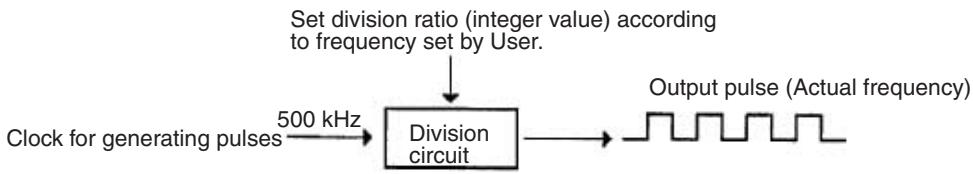
flowchart
graph LR
    A["Clock for generating pulses"] --> B["500 kHz"]
    B --> C["Division circuit"]
    C --> D["Output pulse (Actual frequency)"]
    E["Set division ratio (integer value) according to frequency set by User."] --> C
Actual frequency (kHz) = 500 (kHz) / INT(500 (kHz) / Set frequency (kHz))
INT: Function to derive integer value
INT (500 / Set frequency): Division ratio
The difference between the set frequency and the actual frequency increases as the frequency increases, as shown in the examples in the following table.
| Set frequency (kHz) | Actual frequency (kHz) |
| 45.46 to 50.00 | 50.00 |
| 41.67 to 45.45 | 45.45 |
| 38.47 to 41.66 | 41.67 |
| 31.26 to 33.33 | 33.33 |
| 29.42 to 31.25 | 31.25 |
| 27.78 to 29.41 | 29.41 |
| 20.01 to 20.83 | 20.83 |
| 19.24 to 20.00 | 20.00 |
| 18.52 to 19.23 | 19.23 |
| 10.01 to 10.20 | 10.20 |
| 9.81 to 10.00 | 10.00 |
| 9.62 to 9.80 | 9.80 |
| 5.01 to 5.05 | 5.05 |
| 4.96 to 5.00 | 5.00 |
| 4.90 to 4.95 | 4.95 |
| 3.02 to 3.03 | 3.03 |
| 3.00 to 3.01 | 3.01 |
| 2.98 to 2.99 | 2.99 |
2-3 Absolute Encoder Interface Board
2-3-1 Model
| Name | Model | Specifications |
| Absolute Encoder Interface Board | CQM1H-ABB21 | 2 inputs for absolute encoders |
2-3-2 Functions
Absolute High-speed Counter with Interrupt Function
The Absolute Encoder Interface Board is an Inner Board that counts two gray binary code inputs from an absolute (ABS) rotary encoder.
The Absolute Encoder Interface Board reads binary gray codes (inverted binary codes) input from an absolute encoder through ports 1 and 2 at a maximum counting rate of 4 kHz, and performs processing according to the input values.
Operating Modes
BCD Mode and 360° Mode.
Resolutions
One of the following can be set: 8 bits (0 to 255), 10 bits (0 to 1023), or 12 bits (0 to 4095). The resolution should be set to match that of the encoder connected.
Interrupts
An interrupt subroutine can be executed when the PV (present value) of the absolute high-speed counter matches a specified target value or lies within a specified comparison range.
Note The use of an absolute encoder means that the position data can be retained even during power interrupts, removing the need to perform an origin return when power is returned. In addition, the origin compensation function allows the user to specify any position as the origin.
2-3-3 System Configuration
Detects angle of rotation and controls processing table.
2-3-4 Applicable Inner Board Slots
The Absolute Encoder Interface Board can only be mounted in slot 2 (right slot) of the CQM1-CPU51/61 CPU Unit.
2-3-5 Names and Functions
The Absolute Encoder Interface Board is provided with port 1 connector CN1 and port 2 connector CN2 to receive binary gray code input from absolute rotary encoders.
LED Indicators
| Encoder input indicators | Function | |
| Port 1 | Port 2 | |
| IN1 | IN2 | Lit when input bit 0 is ON. |
| INC1 | INC2 | Lit when value input is incremented. |
| DEC1 | DEC2 | Lit when value input is decremented. |
2-3-6 Absolute Encoder Input Specifications
Instructions
| Instruction | Meaning |
| (@)CTBL(63) | Used to register target or range comparison tables or to start comparisons for previously registered comparison tables. |
| (@)INI(61) | Used to start or stop comparison using registered comparison table or to change the PV of a high-speed counter. |
| (@)PRV(62) | Used to read the PV or status of a high-speed counter. |
| (@)INT(89) | Used to perform mask all interrupts, such as input interrupts, interval timer interrupts, and high-speed counter interrupts. |
Relevant Flags and Bits
Bits for Absolute Encoder Interface Board in Slot 2
| Word | Bits | Name | Function | |
| IR 232 | 00 to 15 | Port 1 | PV word (rightmost four bits) | The PV of the absolute high-speed counter attached to port 1 of the Absolute Encoder Interface Board is stored as an 8-digit BCD after each cycle. |
| IR 233 | 00 to 15 | PV word (leftmost four bits) | ||
| IR 234 | 00 to 15 | Port 2 | PV word (rightmost four bits) | |
| IR 235 | 00 to 15 | PV word (leftmost four bits) | ||
| IR 236 to IR 243 | 00 to 15 | Not used. | --- | |
AR Flags
| Word | Bit | Name | Function | ||
| AR 05 | 00 | Port 1 | High-speed Counter Range Comparison Flags | ON when counter PV satisfies conditions for comparison range 1 | When using high-speed counter 1 in range comparison mode, each bit turns ON when the corresponding condition is satisfied. |
| 01 | ON when counter PV satisfies conditions for comparison range 2 | ||||
| 02 | ON when counter PV satisfies conditions for comparison range 3 | ||||
| 03 | ON when counter PV satisfies conditions for comparison range 4 | ||||
| 04 | ON when counter PV satisfies conditions for comparison range 5 | ||||
| 05 | ON when counter PV satisfies conditions for comparison range 6 | ||||
| 06 | ON when counter PV satisfies conditions for comparison range 7 | ||||
| 07 | ON when counter PV satisfies conditions for comparison range 8 | ||||
| 08 | High-speed Counter Comparison Flag | Indicates status of comparison operation.OFF: StoppedON: Comparing | |||
| AR 06 | 00 | Port 2 | High-speed Counter Range Comparison Flags | ON when counter PV satisfies conditions for comparison range 1 | When using high-speed counter 2 in range comparison mode, each bit turns ON when the corresponding condition is satisfied. |
| 01 | ON when counter PV satisfies conditions for comparison range 2 | ||||
| 02 | ON when counter PV satisfies conditions for comparison range 3 | ||||
| 03 | ON when counter PV satisfies conditions for comparison range 4 | ||||
| 04 | ON when counter PV satisfies conditions for comparison range 5 | ||||
| 05 | ON when counter PV satisfies conditions for comparison range 6 | ||||
| 06 | ON when counter PV satisfies conditions for comparison range 7 | ||||
| 07 | ON when counter PV satisfies conditions for comparison range 8 | ||||
| 08 | High-speed Counter Comparison Flag | Indicates status of comparison operation.OFF: StoppedON: Comparing | |||
SR Area Flags
| Word | Bit | Function |
| IR 252 | 01 | Absolute High-speed Counter 1 Origin Compensation Bit (Port 1) |
| 02 | Absolute High-speed Counter 2 Origin Compensation Bit (Port 2) | |
| IR 254 | 15 | Inner Board Error Flag |
AR Area Bit
| Word | Bits | Name | Function |
| AR 04 | 08 to 15 | Error code for Inner Board in slot 2 | 00 Hex: No error01 or 02 Hex: Hardware error03 Hex: PC Setup error |
Related PC Setup Settings
| Word | Bits | Function | When setting is activated | |
| DM 6611 | 00 to 15 | Stored origin compensation value (BCD) for port 1 | 0000 to 4095 (4-digit BCD)The origin is compensated when the Origin Compensation Bit (SR 25201 for port 1, SR 25202 for port 2) is turned ON. The compensation value is set as a 4-digit BCD between 0000 and 4095 in either BCD Mode or 360° Mode. | When Origin Compensation Bit turns ON in PROGRAM mode. |
| DM 6612 | 00 to 15 | Stored origin compensation value (BCD) for port 2 | ||
| DM 6643 | 00 to 07 | Port 1 | Resolution00 Hex: 8 bits01 Hex: 10 bits02 Hex: 12 bits | When operation starts. |
| 08 to 15 | Operating mode settings00 Hex: BCD Mode01 Hex: 360° Mode | |||
| DM 6644 | 00 to 07 | Port 2 | Resolution00 Hex: 8 bits01 Hex: 10 bits02 Hex: 12 bits | |
| 08 to 15 | Operating mode settings00 Hex: BCD Mode01 Hex: 360° Mode | |||
2-3-7 High-speed Counter Interrupts
The Absolute Encoder Interface Board interfaces an absolute encoder. Interrupt processing can be performed in response to binary gray code signals input to ports 1 or 2 from an absolute rotary encoder.
The two ports can be operated separately. The counter for port 1 is called absolute high-speed counter 1 and the counter for port 2 is called absolute high-speed counter 2. This section describes how to use absolute high-speed counters 1 and 2. The counting rate is 4 kHz.
Processing
Input Signals and Operating Modes
There are two operating modes that can be used for absolute high-speed counters 1 and 2.
1,2,3...
1. BCD Mode:
The absolute rotary encoder's binary gray code is first converted to normal binary (hexadecimal) data, and then converted to BCD.
2. 360° Mode:
With the maximum value of the resolution taken to be 360^ , the input from the absolute rotary encoder is converted to an angle between 0^ and 359^ . CTBL(63) settings are made in 5^ units.
The resolution of the binary gray code inputs to ports 1 and 2 must be one of the three resolutions listed in the following table. The table also shows the range of values associated with each resolution in each operating mode.
| Resolution | Possible PVs | |
| BCD Mode | 360° Mode | |
| 8-bit | 0 to 255 | PV output: 0° to 359° (1° units)Comparison table settings: 0° to 355° (5° units) |
| 10-bit | 0 to 1023 | |
| 12-bit | 0 to 4095 | |
Setting Absolute High-speed Counter in 360° Mode
The following table shows how the settings, which are made in units of 5^ , are converted into binary gray codes according to the resolution.
5^ to 45^
| Resolution | 5^ | 10^ | 15^ | 20^ | 25^ | 30^ | 35^ | 40^ | 45^ |
| 8-bit | 4 | 7 | 11 | 14 | 18 | 21 | 25 | 28 | 32 |
| 10-bit | 14 | 28 | 43 | 57 | 71 | 85 | 100 | 114 | 128 |
| 12-bit | 57 | 114 | 171 | 228 | 284 | 341 | 398 | 455 | 512 |
50° to 355°
Based on the conversions in the range 5^ to 45^ given above, conversions for the remaining values are calculated as follows:
Setting (°) ÷ 45° = A with B(°) remaining.
Conversion = (Conversion of 45°) x A + (Conversion of B)
E.g., 145^ at a resolution of 8 bits
145^ ÷ 45^ = 3 with 10^ remaining.
Therefore, converted value = 32 x 3 + 7 = 103
At resolutions of 10 and 12 bits, it is possible that small differences in computations may result in interrupt processing not being executed even when the PV matches the comparison conditions.
Absolute High-speed Counter Interrupt Count
The counter's PV can be checked using the following two methods:
- Target value method
- Range comparison method
Refer to page 36 for a description of each method.
Procedure for Using Absolute High-speed Counters
flowchart
graph TD
    A["Determine operating mode and resolution."] --> B["Mount Board and wire inputs."]
    B --> C["PC Setup (DM 6643/DM 6644)"]
    C --> D["Origin compensation\nSet encoder to position desired as origin.\nCheck PV of absolute high-speed counter\n1 or 2 (IR 232/IR 233 or IR 234/IR 235).\nTurn ON Origin Compensation Bit for absolute high-speed counter (SR 25201 or SR 25201).\nThe origin compensation (4-digit BCD) will be stored in PC Setup (DM 6611 or DM 6612).\nVerify that 0000 is stored as the PV of absolute high-speed counter 1 or 2 (IR 232 or IR 234)."]
    D --> E["Ladder program"]
REGISTER COMPARISON TABLE, CTBL(63):
Port-specific comparison table registration and comparison start
MODE CONTROL, INI(61):
Port-specific PV change and comparison start
HIGH-SPEED COUNTER PV READ, PRV(62):
Port-specific high-speed counter PV read; high-speed counter comparison status read; range comparison result read
SUBROUTINE DEFINE, SBN(92) and RETURN, RET(93):
Creation of interrupt subroutine program (Only when using absolute high-speed counter 1 and 2 interrupts.)
High-speed Counter Function
flowchart
graph TD
    A["Pin No."] --> B["Bit 1 (15)"]
    A --> C["Bit 2^0 (7)"]
    A --> D["Bit 2^1 (14)"]
    A --> E["Bit 2^2 (6)"]
    A --> F["... (13)"]
    A --> G["... (5)"]
    A --> H["... (12)"]
    A --> I["... (4)"]
    A --> J["Bit 2^9 (11)"]
    A --> K["Bit 2^10 (3)"]
    A --> L["Bit 2^11 (2)"]
    A --> M["Bit 2^0 (15)"]
    A --> N["... (1)"]
    A --> O["Bit 2^11 (2)"]

    B --> P["Mode/Resolution"]
    P --> Q["BCD Mode/360 Mode 8-bit, 10-bit, or 12-bit"]
    Q --> R["Origin compensation"]
    R --> S["Port 1: SR 25201<br>Port 2: SR 25202"]
    S --> T["Count"]
    T --> U["Ladder Program"]
    U --> V["CTBL(63)"]
    U --> W["REGISTER COMPARISON TABLE"]
    U --> X["Table registration Comparison start"]
    U --> Y["INI(61)"]
    U --> Z["MODE CONTROL"]
    U --> AA["PV change Comparison start/stop"]

    V --> AB["Count check interrupt"]
    W --> AC["Interrupt Subroutine"]
    X --> AD["Not specified subroutine executed"]
    Y --> AE["Not specified subroutine executed"]
    Z --> AF["Not specified subroutine executed"]

    subgraph "Each cycle"
        G
        N
    end

    subgraph "Each execution"
        U
        V
        W
        X
        Y
        Z
        AA
    end

    G --> G1["PVs of counters<br>Port 1: IR 233 IR 232<br>Port 2: IR 235 IR 234"]
    V --> V1["PRV (62)"]
    V --> V2["HIGH-SPEED COUNTER PV READ"]
    V --> V3["PV read<br>Comparison operation status read<br>Range comparison result read"]

    subgraph "Count check interrupt"
        U
        V
        W
        X
        Y
        Z
        AA
        AB
        AC
        AD
        AE
        AF
        AG
        AH
        AI
        AJ
        AK
        AL
        AM
        AN
        AO
        AP
        AQ
        AR
        AS
        AT
        AU
        AV
        AW
        AX
        AY
        AZ
        BA
        BB
        BC
        BD
        BE
        BF
        BG
        BH
        BI
        BJ
        BK
        BL
        BM
        BN
        BO
        BP
        BPB
        BPB
        BPB
        BPB
        BPB
        BPB
    end

    note right of U: "Each cycle"
    note right of V: "Each execution"
Preliminary PC Setup
Make the following settings in PROGRAM mode before using absolute high-speed counter 1 or 2 interrupts in a program.
Absolute High-speed Counter Settings
DM 6643 contains the settings for absolute high-speed counter 1, and DM 6644 contains the settings for absolute high-speed counter 2. These words determine the operating modes and resolution settings.
Defaults: 0000
(BCD Mode, 8-bit resolution)
Input Refresh Word Settings
DM 6634 contains the input refresh word settings for absolute high-speed counter 1, and DM 6635 contains the settings for absolute high-speed counter 2. Make these settings when it is necessary to refresh inputs.

Default: 0000 (No inputs refreshed)
Origin Compensation
It is possible to compensate for a discrepancy between an absolute encoder's origin and the actual origin. After origin compensation has been set, the data from the absolute encoder will be adjusted before being output as the PV. Once set, the origin compensation will remain in effect until the next origin compensation is executed; it remains in effect even after power has been turned OFF. Origin compensation can be set separately for ports 1 and 2.
The default setting is for no origin compensation.
Follow the procedure below to set origin compensation.
1,2,3...
- Set the absolute encoder to the desired origin location.
- Make sure that pin 1 of the CQM1H CPU Unit's DIP switch is OFF (enabling Programming Devices to write DM 6144 through DM 6568), then switch the PC to PROGRAM mode.
- Set the absolute resolution in DM 6643 or DM 6644.
- Make sure that a fatal error or FALS 9C error has not occurred.
- Read the absolute high-speed counter's PV from IR 232 and IR 233 (port 1) or IR 234 and IR 235 (port 2) to determine the value before origin compensation.
- Turn ON the Absolute High-speed Counter 1 Origin Compensation Bit (SR 25201) or Absolute High-speed Counter 2 Origin Compensation Bit (SR 25202) from a Programming Device.
The compensation value will be written to DM 6611 (port 1) or DM 6612 (port 2) and the Origin Compensation Bit will be turned OFF automatically. The compensation value will be stored as a 4-digit BCD between 0000 and 4095 regardless of whether the counter is set to BCD mode or 360° mode. - Read the high-speed counter's PV word to verify that origin compensation has completed normally. (The PV should be 0000 after origin compensation.)
The compensation value will remain in effect until it is changed again by the procedure above.
Programming
Use the following steps to program absolute high-speed counters 1 and 2.
Absolute high-speed counters 1 and 2 begin counting when the PC Setup settings are enabled, but comparisons will not be made with the comparison table and interrupts will not be generated unless the CTBL(63) instruction is executed.
The PV of absolute high-speed counter 1 is maintained in IR 232 and IR 233, and the PV of absolute high-speed counter 2 is maintained in IR 234 and IR 235.
Starting and Stopping Comparisons
1,2,3... 1. Use the CTBL(63) instruction to save the comparison table in the CQM1H and begin comparisons.
P: Port
001: Port 1
002: Port 2
C: Mode (3-digit BCD)
000: Target value table registration and comparison start
001: Range comparison table registration and comparison start
002: Target value table registration only
003: Range comparison table registration only
TB: First word of comparison table
P specifies the port. Set P=001 to specify absolute high-speed counter 1 (i.e., port 1), or P=002 to specify absolute high-speed counter 2 (port 2).
Setting 000 as the value of C registers a target value comparison table, and setting 001 registers a range comparison table. Comparison begins upon completion of this registration. While comparisons are being performed, absolute high-speed counter interrupts will be executed according to the applicable comparison table. Refer to 5-16-7 REGISTER COMPARISON TABLE – CTBL(63) for details on comparison table registration.
If C is set to 002, then comparisons will be made using the target value method; if 003, then they will be made using the range comparison method. In both cases the comparison table will be saved but comparisons will not actually begin until INI(61) is used.
Note Unlike other high-speed counters, the interrupts of absolute high-speed counters 1 and 2, the target value, and upper and lower limits registered in the comparison table are all set in one word each.
- To stop comparisons, execute INI(61) as shown below. Specify port 1 or 2 in P (P=001 or 002).
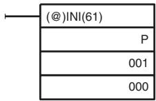
P: Port
001: Port 1
002: Port 2
To restart comparisons, set the first operand to the port number, and the second operand to 000 (execute comparison), and execute INI(61).
A table that has been saved will be retained in the CQM1H during operation (i.e., during program execution) until a new table is saved.
Reading the PV of Absolute High-speed Counters 1 and 2
The following two methods can be used to read the PVs of absolute high-speed counters 1 and 2:
- Reading PVs from memory (IR 232 or IR 234)
- Using PRV(62)
Reading PVs from Memory
The PVs of high-speed counters 1 and 4 are stored in the data area words as 8-digit BCDs, regardless of whether the Board is in BCD Mode or 360° Mode.
| Leftmost4 digits | Rightmost4 digits | BCD Mode | 360° Mode | |
| Port 1: | IR 233 | IR 232 | 0000 0000 to 0000 4095 | 0000 0000 to 0000 0359 |
| Port 2: | IR 235 | IR 234 |
Note These words are refreshed only once every cycle, so they may differ from the actual PV.
Using PRV(62)
PRV(62) is used to read the PVs of absolute high-speed counters 1 and 2. Specify absolute high-speed counter 1 or 2 in P (P=001 or 002).
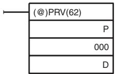
P: Port
001: Port 1
002: Port 2
D: First destination word
The PV of the specified absolute high-speed counter is stored as shown below. The PV is stored as 8-digit BCD, regardless of whether the Board is in BCD Mode or 360° Mode.
Leftmost
4 digits

Rightmost
4 digits

BCD Mode
0000 0000 to 0000 4095
360° Mode
0000 0000 to 0000 0359
Note The PV can be read accurately at the time PRV(62) is executed.
Reading Absolute High-speed Counter Status
There are two ways to read the status of high-speed counters 1 and 2:
- Reading AR area flags
- Using PRV(62)
Reading AR Area Flags
The CQM1H words relating to absolute high-speed counters 1 and 2 are listed below. It is possible to determine the status of absolute high-speed counters 1 and 2 by reading these data words.
- Inner Board Error Codes
| Word | Bits | Function | |
| AR 04 | 08 to 15 | Slot2 | The stored error codes are as follows:00 Hex: Normal01 or 02 Hex: Hardware error03 Hex: PC Setup error |
- Words Indicating Operational Status
| Word | Bit | Name | Function | ||
| Counter 1 | Counter 2 | ||||
| AR 05 | AR 06 | 00 | High-speed Counter Range Comparison Flags | ON when meeting first condition. | When the high-speed counter is used in range comparison format, a bit turns ON when the corresponding condition is met. |
| 01 | ON when meeting second condition. | ||||
| 02 | ON when meeting third condition. | ||||
| 03 | ON when meeting fourth condition. | ||||
| 04 | ON when meeting fifth condition. | ||||
| 05 | ON when meeting sixth condition. | ||||
| 06 | ON when meeting seventh condition. | ||||
| 07 | ON when meeting eighth condition. | ||||
| 08 | High-speed Counter Comparison Flag | Indicates the status of the comparison operation.0: Stopped1: Running | |||
Using PRV(62)
The status of absolute high-speed counters 1 and 2 can also be determined by executing PRV(62). Specify high-speed counter 1 or 2 (P=001 or 002) and the destination word D.
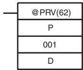
P: Port 001: Port 1 002: Port 2 D: First destination word
The status of the specified high-speed counter is stored in bit 00 of D, as shown in the following table.
| Bit | Function |
| 00 | Comparison Operation Flag (0: Stopped; 1: Running) |
Bits 01 to 15 are set to 0.
Operation Example
This example shows programming that receives an input signal from an absolute rotary encoder at port 1 and uses this input to control outputs IR 10000 through IR 10003. Absolute high-speed counter 1 is set for 8-bit resolution and 360° Mode, and range comparisons are performed. Before executing the program, set DM 6643 to 0100 (Port 1: 360° Mode, 8-bit resolution).
Other PC Setup settings use the default settings. (Inputs are not refreshed at the time of interrupt processing.)
In addition, the following data is stored for the comparison table:
| DM 0000 | 0000 | Lower limit #1 (0°) |
| DM 0001 | 0085 | Upper limit #1 (85°) |
| DM 0002 | 0100 | Subroutine number 100 |
| DM 0003 | 0090 | Lower limit #2 (90°) |
| DM 0004 | 0175 | Upper limit #2 (175°) |
| DM 0005 | 0101 | Subroutine number 101 |
| DM 0006 | 0180 | Lower limit #3 (180°) |
| DM 0007 | 0265 | Upper limit #3 (265°) |
| DM 0008 | 0102 | Subroutine number 102 |
| DM 0009 | 0270 | Lower limit #4 (270°) |
| DM 0010 | 0355 | Upper limit #4 (355°) |
| DM 0011 | 0103 | Subroutine number 103 |
| DM 0012 | 0000 | Lower limit #1 (0°) |
| DM 0013 | 0000 | Upper limit #1 (0°) |
| DM 0014 | FFFF | No subroutine number |
| DM 0015 | 0000 | Lower limit #1 (0°) |
| DM 0016 | 0000 | Upper limit #1 (0°) |
| DM 0017 | FFFF | No subroutine number |
| DM 0018 | 0000 | Lower limit #1 (0°) |
| DM 0019 | 0000 | Upper limit #1 (0°) |
| DM 0020 | FFFF | No subroutine number |
| DM 0021 | 0000 | Lower limit #1 (0°) |
| DM 0022 | 0000 | Upper limit #1 (0°) |
| DM 0023 | FFFF | No subroutine number |
In 360^ Mode, upper and lower limits are set in units of 5^ .
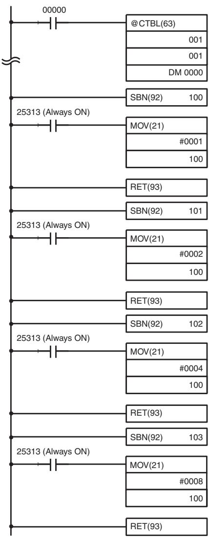
flowchart
graph TD
    A["00000"] --> B["@CTBL(63)"]
    B --> C["001"]
    B --> D["001"]
    B --> E["DM 0000"]
    F["25313 (Always ON)"] --> G["SBN(92) 100"]
    H["25313 (Always ON)"] --> I["MOV(21) #0001 100"]
    J["25313 (Always ON)"] --> K["RET(93)"]
    L["25313 (Always ON)"] --> M["SBN(92) 101"]
    N["25313 (Always ON)"] --> O["MOV(21) #0002 100"]
    P["25313 (Always ON)"] --> Q["RET(93)"]
    R["25313 (Always ON)"] --> S["SBN(92) 102"]
    T["25313 (Always ON)"] --> U["MOV(21) #0004 100"]
    V["25313 (Always ON)"] --> W["RET(93)"]
    X["25313 (Always ON)"] --> Y["SBN(92) 103"]
    Z["25313 (Always ON)"] --> AA["MOV(21) #0008 100"]
    AB["RET(93)"] --> AC["RET(93)"]
Specifies port 1, saves the comparison table in range matching format, and begins comparing.
Turns ON IR 10000. Turns OFF other bits in IR 100.
Turns ON IR 10001. Turns OFF other bits in IR 100.
Turns ON IR 10002. Turns OFF other bits in IR 100.
Turns ON IR 10003. Turns OFF other bits in IR 100.
The following diagram shows the relationship between the PV of absolute high-speed counter 1 and Range Comparison Result Flags AR 0500 to AR 0507 as the above instructions are executed.
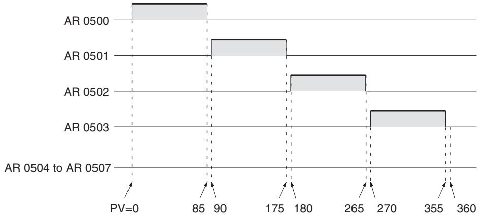
bar
| Category | Value | |---|---| | AR 0500 | 100 | | AR 0501 | 80 | | AR 0502 | 60 | | AR 0503 | 40 | | AR 0504 to AR 0507 | 30 | PV=0, 85, 90, 175, 180, 265, 270, 355, 3602-4 Analog Setting Board
2-4-1 Model
| Name | Model | Specifications |
| Analog Setting Board | CQM1H-AVB41 | Four analog setting screws |
2-4-2 Function
Each of the values set using the four variable resistors located on the front of the Analog Settings Board is stored as a 4-digit BCD between 0000 and 0200 in the analog settings words (IR 220 to IR 223).
By using the Analog Setting Board, an operator can, for example, set the value of a timer instruction using an analog setting (IR 220 to IR 223), and thereby slightly speed up or slow down the speed or timing of a conveyor belt simply by adjusting a control with a screwdriver, removing the need for a Programming Device.
Using the Analog Timer
The following example shows the 4-digit BCD setting (0000 to 0200) stored in IR 220 to IR 223 being used as a timer setting.
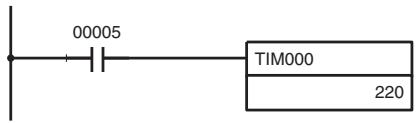
The setting of TIM000 is set externally in IR 220. (Timer is executed using the setting of analog control 0.)
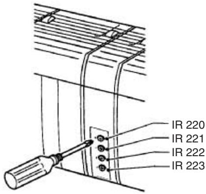
Phillips screwdriver
2-4-3 Applicable Inner Board Slots
The Analog Setting Board can be installed in either slot 1 (left slot) or slot 2 (right slot) of the CQM1H-CPU51/61 CPU Unit. Both slots, however, cannot be used at the same time.
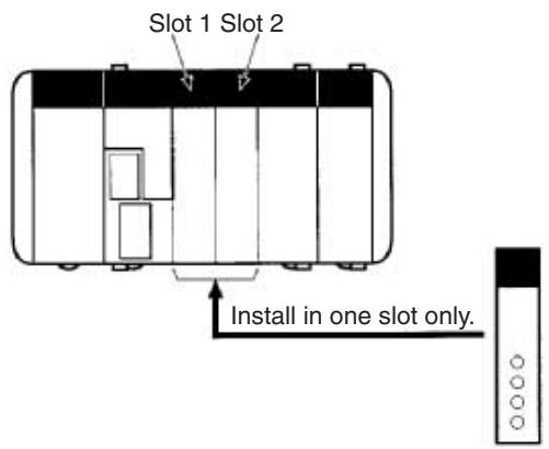
2-4-4 Names and Functions
The four analog controls of the Analog Setting Board are located on the front panel. The front panel does not have any indicators.
The value of the setting increases as the control is rotated clockwise. Use a small Phillips screwdriver for this purpose.
Specifying IR 220 to IR 223 as the set value of a TIM instruction enables the Board to be used as an analog timer. When the timer is started, the analog settings are stored as the timer set value.
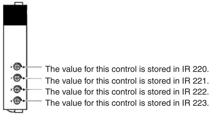

While the power is turned ON, the contents of IR 220 to IR 223 are constantly refreshed with the values of the corresponding controls. Be sure that these words are not written to from the program or a Programming Device.
2-4-5 Specifications
Relevant Bits
The values of the Analog Setting Board analog controls are stored in the following addresses of the Inner Board area regardless of the slot in which the Board is mounted.
| Word | Bits | Name | Function |
| IR 220 | 00 to 15 | Analog control 1 | With each cycle, the values of analog controls 0 to 3 are stored as 4-digit BCD values between 0000 and 0200. |
| IR 221 | 00 to 15 | Analog control 2 | |
| IR 222 | 00 to 15 | Analog control 3 | |
| IR 223 | 00 to 15 | Analog control 4 |
Related PC Setup Settings None
2-5 Analog I/O Board
2-5-1 Model
| Name | Model | Specifications |
| Analog I/O Board | CQM1H-MAB42 | 4 analog inputs ( -10 to +10 V; 0 to 5 V; 0 to 20 mA; separate signal range for each point)2 analog outputs ( -10 to +10 V; 0 to 20 mA; separate signal range for each point) |
2-5-2 Function
The Analog I/O Board is an Inner Board featuring four analog inputs and two analog outputs.
The signal ranges that can be used for each of the four analog input points are -10 to +10 V, 0 to 5 V, and 0 to 20 mA. A separate range is set for each point. The settings in DM 6611 determine the signal ranges.
The signal ranges that can be used for each of the two analog output points are -10 to +10 V and 0 to 20 mA. A separate signal range can be selected for each point. The settings in DM 6611 determine the signal range.
2-5-3 System Configuration
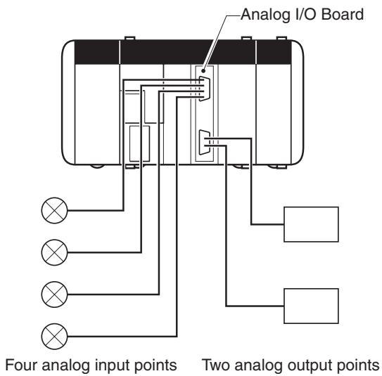
2-5-4 Applicable Inner Board Slot
The Analog I/O Board can only be mounted in slot 2 (right slot) of the CQM1H-CPU51/61 CPU Unit.
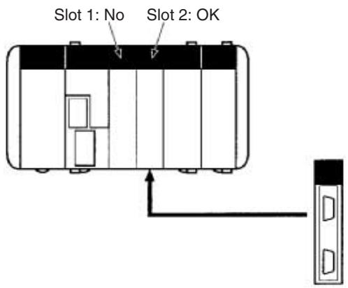
2-5-5 Names and Functions
The Analog I/O Board has a CN1 connector for the four analog inputs and a CN2 connector for 2 analog outputs.
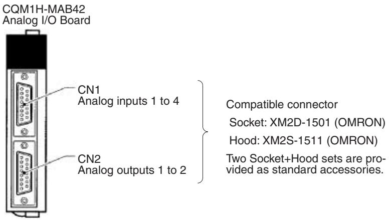
LED Indicators
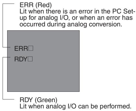
2-5-6 Specifications
Analog Inputs: Input Data and Converted Values
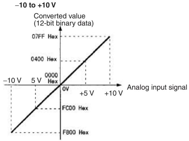
line
| Analog input signal | Converted value (Hex) | | ------------------- | --------------------- | | -10 V | -10 | | 5 V | 0 | | 0V | 07FF | | +5 V | 0400 | | +10 V | 0000 | | +10 V | 07FF | | +10 V | 0400 | | +10 V | 0000 | | +10 V | 07FF | | +10 V | 0400 | | +10 V | 0000 | | +10 V | 07FF | | +10 V | 0400 | | +10 V | 0256 | | +10 V | 0256 | | +10 V | 0256 | | +10 V | 0256 | | +10 V | 0256 | | +10 V | 0256 | | +10 V | 0256 | | +10 V | 0256 |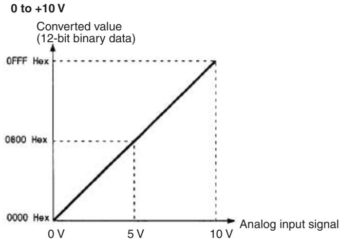
line
| Analog input signal | Converted value (12-bit binary data) | | ------------------- | ------------------------------------- | | 0 V | 0000 Hex | | 5 V | 0800 Hex | | 10 V | 0FFF Hex |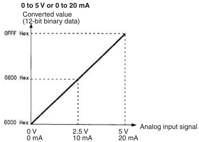
line
0 to 5V or 0 to 20mA Converted value (12-bit binary data) Analog input signal | Analog input signal (V) | Converted value (Hex) | | :--- | :--- | | 0 V 0 mA | 0.000 | | 2.5 V 10 mA | 0800 | | 5 V 20 mA | 0FFF |Analog Outputs: Settings and Output Data
line
| Hex | Analog output signal | | ------ | -------------------- | | 0 | 0 | | 0000 | +5 | | 0400 | +10 | | 07FF | +10 |
line
| Setting (11-bit binary data) | Analog output signal (mA) | | ---------------------------- | ------------------------- | | 0000 Hex | 0 | | 0400 Hex | 10 | | 07FF Hex | 20 |Applications Examples
The Board uses no special instructions. MOV(21) is used to read analog input values and set analog output values.
Relevant Bits
Bits Used by Inner Board in Slot 2
| Word | Bits | Name | Function |
| IR 232 | 00 to 15 | Analog input 1 converted value | The converted value from each input from the Analog I/O Board is stored as a 4-digit Hex each cycle. -10 to +10 V: F800 to 07FFF Hex0 to 10 V: 0000 to 0FFF Hex0 to 5 V/0 to 20 mA: 0000 to 0FFF Hex |
| IR 233 | 00 to 15 | Analog input 2 converted value | |
| IR 234 | 00 to 15 | Analog input 3 converted value | |
| IR 235 | 00 to 15 | Analog input 4 converted value | |
| IR 236 | 00 to 15 | Analog output 1 setting | The setting of each output from the Analog I/O Board is stored as a 4-digit Hex. (Read each cycle.) -10 to +10 V: F800 to 07FF Hex0 to 20 mA: 0000 to 07FF Hex |
| IR 237 | 00 to 15 | Analog output 2 setting |
SR Area Flags
| Word | Bit | Function |
| SR 254 | 15 | Inner Board Error Flag |
AR Area Flags
| Word | Bits | Function | |
| AR 04 | 08 to 15 | Error codes for Inner Board in slot 2 | 00 Hex: Normal01 or 02 Hex: Hardware error03 Hex: PC Setup error04 Hex: A/D or D/A conversion error |
Relevant PC Setup Settings
| Word | Bits | Function | |
| DM 6611 | 00 to 07 | 00, 01: Analog input 1 input signal range02, 03: Analog input 2 input signal range04, 05: Analog input 3 input signal range06, 07: Analog input 4 input signal range | 00: -10 to +10 V01: 0 to 10 V10: 0 to 5 V/0 to 20 mA11: Not used.(0 to 20 mA are distinguished by the connected terminal.) |
| 08 | Analog input 1 usage selection | Specifies use or non-use of A/D conversion for each port.0: Use input (conversion)1: Do not use input (no conversion) | |
| 09 | Analog input 2 usage selection | ||
| 10 | Analog input 3 usage selection | ||
| 11 | Analog input 4 usage selection | ||
| 12 to 15 | Not used. (Fixed at 0.) | ||
Note The level of the analog output signal is determined by the connected terminal, and there is no PC Setup setting. These settings are reflected in status at power ON.
2-5-7 Application Procedure
flowchart
graph TD
    A["Determine analog input ranges and number of inputs\nDetermine analog output ranges and number of outputs."] --> B["Wire analog inputs and analog outputs."]
    B --> C["PC Setup (DM 6611)"]
    C --> D["Ladder Program"]
    E["0 to 5 V and 0 to 20 mA analog inputs are selected by the terminals connected.\n0 to 5 V and 0 to 20 mA analog outputs are selected by the terminals connected."] --> F["Set signal ranges for analog inputs.\nSet whether or not to use analog inputs."]
    G["Analog inputs: Read converted values.\nAnalog outputs: Write settings."] --> H["End"]
2-6 Serial Communications Board
This section provides an introduction to the Serial Communications Board. Detailed information can be found in the Serial Communications Board Operation Manual (W365).
2-6-1 Model Number
| Name | Model | Specifications |
| Serial Communications Board | CQM1H-SCB41 | One RS-232 portOne RS-422A/485 port |
2-6-2 Serial Communications Boards
The Serial Communications Board is an Inner Board for the CQM1H-series PCs. One Board can be installed in Inner Board slot 1 of a CQM1H-series CPU Unit. The Board cannot be installed in slot 2.
The Board provides two serial communications ports for connecting host computers, Programmable Terminals (PTs), general-purpose external devices, and Programming Devices (excluding Programming Consoles). This makes it possible to easily increase the number of serial communications ports for a CQM1H-series PC.
2-6-3 Features
The Serial Communications Board is an option that can be mounted in the CPU Unit to increase the number of serial ports without using an I/O slot. It supports protocol macros (which are not supported by the ports built into the CPU Units), allowing easy connection to general-purpose devices that have a serial port.
flowchart
graph TD
    A["Inside controlled machine"] --> B["Serial Communications Board"]
    B --> C["RS-232C"]
    C --> D["RS-422A/485"]
    D --> E["Temperature controller or other device"]
    D --> F["External device with RS-232C or RS-422A/485 port"]
    G["Bar code reader or other device"] --> H["OR"]
    I["Dedicated controller or other device"] --> J["External device with RS-232C or RS-422A/485 port"]
Both RS-232C and RS-422A/485 ports are provided. The RS-422A/485 port enables 1:N connections to general-purpose external devices without going through Converting Link Adapters. The 1:N connections can be used with protocol macros or 1:N-mode NT Links.
2-6-4 System Configuration
The following serial communications modes are supported by the Serial Communications Board: Host Link (SYSMAC WAY), protocol macro, no-protocol, 1:1 Data Links, 1:N-mode NT Link, and 1:1-mode NT Link modes. The devices shown in the following diagram can be connected.
Note The 1:1-mode NT Link and 1:N-mode NT Link communications modes use different protocols that are not compatible with each other.
flowchart
graph TD
    A["RS-232C"] --> B["RS-422A/485"]
    B --> C["No-protocol"]
    B --> D["General-purpose external device"]
    B --> E["Programmable Terminal (PT)"]
    B --> F["C-series PC"]
    B --> G["1:1 Data Link"]
    B --> H["Host Link"]
    B --> I["Host Computer"]
    B --> J["RT Link"]
    B --> K["NT Link"]
    B --> L["Data Link"]
    style A fill:#f9f,stroke:#333
    style B fill:#ccf,stroke:#333
    style C fill:#cfc,stroke:#333
    style D fill:#fcc,stroke:#333
    style E fill:#fcc,stroke:#333
    style F fill:#fcc,stroke:#333
    style G fill:#fcc,stroke:#333
    style H fill:#fcc,stroke:#333
    style I fill:#fcc,stroke:#333
    style J fill:#fcc,stroke:#333
    style K fill:#fcc,stroke:#333
    style L fill:#fcc,stroke:#333
Note An NT-AL001-E Converting Link Adapter can be used to convert between RS-232C and RS-422A/485. This Link Adapter requires a 5-V power supply. Power is provided by the RS-232C port on the Serial Communications Board when the Link Adapter is connected to it, but must be provided separately when connecting the Link Adapter to other devices.
SECTION 3
Memory Areas
This section describes the structure of the CQM1H PC memory areas and explains how to use them. It also describes the Memory Cassette operations used to transfer data between the CPU Unit and a Memory Cassette.
3-1 Memory Area Structure 146
3-2 IR Area 148
3-2-1 Input and Output Areas.... 148
3-2-2 Work Areas.... 148
3-2-3 I/O Allocation.... 148
3-2-4 Flags/Bits for an Inner Board in Slot 1 (IR 200 to IR 215) ..... 155
3-2-5 Flags/Bits for an Inner Board in Slot 2 (IR 232 to IR 243) ..... 158
3-2-6 Flags/Bits for Communications Units 159
3-3 SR Area.... 160
3-4 TR Area.... 163
3-5 HR Area 163
3-6 AR Area 164
3-6-1 Shared Flags/Bits (AR 00 to AR 04) 164
3-6-2 Flags/Bits for Inner Boards (AR 05 and AR 06) ..... 165
3-6-3 Shared Flags/Bits (AR 07 to AR 27) 167
3-6-4 Using the Clock 170
3-7 LR Area.... 171
3-8 Timer/Counter Area 172
3-9 DM Area 172
3-10 EM Area 174
3-11 Using Memory Cassettes 174
3-11-1 Memory Cassettes and Contents.... 174
3-11-2 Memory Cassette Capacity and Program Size 175
3-11-3 Writing to the Memory Cassette.... 177
3-11-4 Reading from the Memory Cassette.... 177
3-11-5 Comparing Memory Cassette Contents 178
3-1 Memory Area Structure
The following memory areas can be used with the CQM1H.
| Data area | Size | Words | Bits | Function | |
| IR area (note 1) | Input area | 256 bits | IR 000 to IR 015 | IR 00000 to IR 01515 | Input bits can be allocated to Input Units or I/O Units. The 16 bits in IR 000 are always allocated to the CPU Unit's built-in inputs. |
| Output area | 256 bits | IR 100 to IR 115 | IR 10000 to IR 11515 | Output bits can be allocated to Output Units or I/O Units. | |
| Work areas | 2,528 bits min. (note 2) | IR 016 to IR 089 | IR 01600 to IR 08915 | Work bits do not have any specific function, and they can be freely used within the program. | |
| IR 116 to IR 189 | IR 11600 to IR 18915 | ||||
| IR 216 to IR 219 | IR 21600 to IR 21915 | ||||
| IR 224 to IR 229 | IR 22400 to IR 22915 | ||||
| Controller Link status areas | 96 bits | IR 090 to IR 095 | IR 09000 to IR 09615 | Used to indicate the Controller Link Data Link status information. (Can be used as work bits when a Controller Link Unit is not mounted.) | |
| 96 bits | IR 190 to IR 195 | IR 19000 to IR 19615 | Used to indicate the Controller Link error and network participation information. (Can be used as work bits when a Controller Link Unit is not mounted.) | ||
| MACRO operand area (note 1) | Input area | 64 bits | IR 096 to IR 099 | IR 09600 to IR 09915 | Used when the MACRO instruction, MCRO(99), is used. (Can be used as work bits when the MACRO instruction is not used.) |
| Output area | 64 bits | IR 196 to IR 199 | IR 19600 to IR 19915 | ||
| Inner Board slot 1 area | 256 bits | IR 200 to IR 215 | IR 20000 to IR 21515 | These bits are allocated to the Inner Board mounted in slot 1 of the CQM1H-CPU51/61. (Can be used as work bits when the CQM1H-CPU11/CPU21 is being used or slot 1 is empty.)CQM1H-CTB41 High-speed Counter Board: IR 200 to IR 213 (14 words): Used by the Board IR 214 and IR 215 (2 words): Not used.CQM1H-SCB41 Serial Communications Board: IR 200 to IR 207 (8 words): Used by the Board IR 208 to IR 215 (8 words): Not used. | |
| Analog settings area (note 1) | 64 bits | IR 220 to IR 223 | IR 22000 to IR 22315 | Used to store the analog settings when the CQM1H-AVB41 Analog Setting Board is mounted. (Can be used as work bits when an Analog Setting Board is not mounted.) | |
| High-speed Counter 0 PV (note 1) | 32 bits | IR 230 to IR 231 | IR 23000 to IR 23115 | Used to store the present values of the built-in high-speed counter (high-speed counter 0). (Can be used as work bits when high-speed counter 0 is not being used.) | |
| Inner Board slot 2 area | 192 bits | IR 232 to IR 243 | IR 23200 to IR 24315 | These bits are allocated to the Inner Board mounted in slot 2 of the CQM1H-CPU51/61. (Can be used as work bits when the CQM1H-CPU11/21 is being used or slot 2 is empty.)CQM1H-CTB41 High-speed Counter Board: IR 232 to IR 243 (12 words): Used by the Board CQM1H-PLB21 Pulse I/O Board: IR 232 to IR 239 (8 words): Used by the Board IR 240 to IR 243 (4 words): Not used.CQM1H-ABB21 Absolute Encoder Interface Board: IR 232 to IR 239 (8 words): Used by the Board IR 240 to IR 243 (4 words): Not used.CQM1H-MAB42 Analog I/O Board: IR 232 to IR 239 (8 words): Used by the Board IR 240 to IR 243 (4 words): Not used. | |
| SR area | 184 bits | SR 244 to SR 255 | SR 24400 to SR 25507 | These bits serve specific functions such as flags and control bits. | |
| HR area | 1,600 bits | HR 00 to HR 99 | HR 0000 to HR 9915 | These bits store data and retain their ON/OFF status when power is turned OFF. | |
| AR area | 448 bits | AR 00 to AR 27 | AR 0000 to AR 2715 | These bits serve specific functions such as flags and control bits. | |
| TR area | 8 bits | --- | TR 0 to TR 7 | These bits are used to temporarily store ON/OFF status at program branches. | |
| LR area (note 1) | 1,024 bits | LR 00 to LR 63 | LR 0000 to LR 6315 | Used for 1:1 Data Link through the RS-232 port or through a Controller Link Unit. | |
| Timer/Counter area (note 3) | 512 bits | TIM/CNT 000 to TIM/CNT 511 (timer/counter numbers) | The same numbers are used for both timers and counters. When TIMH(15) is being used, timer numbers 000 to 015 can be interrupt-refreshed to ensure proper timing during long cycles. | ||
| DM area | Read/write | 3,072 words | DM 0000 to DM 3071 | --- | DM area data can be accessed in word units only. Word values are retained when power is turned OFF. |
| 3,072 words | DM 3072 to DM 6143 | --- | Available in CQM1H-CPU51/61 CPU Units only. | ||
| Read-only (note 4) | 425 words | DM 6144 to DM 6568 | --- | Cannot be overwritten from program (only a Programming Device).DM 6400 to DM 6409 (10 words):Controller Link DM parameter areaDM 6450 to DM 6499 (50 words):Routing table areaDM 6550 to DM 6559 (10 words):Serial Communications Board settings | |
| Error log area (note 4) | 31 words | DM 6569 to DM 6599 | --- | Used to store the time of occurrence and error code of errors that occur. | |
| PC Setup (note 4) | 56 words | DM 6600 to DM 6655 | --- | Used to store various parameters that control PC operation. | |
| EM area | 6,144 words | EM 0000 to EM 6143 | --- | EM area data can be accessed in word units only. Word values are retained when power is turned OFF.Available in the CQM1H-CPU61 CPU Unit only. | |
Note
- IR and LR bits that are not used for their allocated functions can be used as work bits.
- A minimum 2,528 bits are available as work bits. Other bits can be used as work bits when they are not used for their allocated functions, so the total number of available work bits depends on the configuration of the PC.
- When accessing a PV, TIM/CNT numbers are used as word data; when accessing Completion Flags, they are used as bit data.
- Data in DM 6144 to DM 6655 cannot be overwritten from the program.
3-2 IR Area
The functions of the IR area are explained below.
3-2-1 Input and Output Areas
IR area bits are allocated to terminals on I/O Output Units and Dedicated I/O Units. They reflect the ON/OFF status of input and output signals. Input bits begin at IR 00000, and output bits begin at IR 10000. With the CQM1H, only IR 00000 through IR 01515 can be used as input bits and only IR 10000 through IR 11515 can be used as output bits.
Note Input bits cannot be used in output instructions. Do not use the same output bit in more than one OUT and/or OUT NOT instruction, or the program will not execute properly.
3-2-2 Work Areas
The work bits can be used freely within the program. They can only be used within the program, however, and not for direct external I/O. Work bits are reset (i.e., turned OFF) when the CQM1H power supply is turned OFF or when operation begins or stops. The following table shows the parts of the IR area that have been set aside for use as work areas.
| Words | Bits |
| IR 016 to IR 089 (74 words) | IR 01600 to IR 08915 (1,184 bits) |
| IR 116 to IR 189 (74 words) | IR 11600 to IR 18915 (1,184 bits) |
| IR 216 to IR 219 (4 words) | IR 21600 to IR 21915 (64 bits) |
| IR 224 to IR 229 (6 words) | IR 22400 to IR 22915 (96 bits) |
The bits in the ranges shown below have specific functions, but can still be used as work bits when their specific functions are not being used.
| Range | Function |
| IR 001 to IR 015 | When allocated to Input Units, these bits serve as input bits. |
| IR 090 to IR 095 | When a Controller Link Unit is mounted to the PC, these bits indicate the status of the Data Link. |
| IR 096 to IR 099 | When the MACRO instruction is used, these bits serve as operand input bits. |
| IR 100 to IR 115 | When allocated to Output Units, these bits serve as output bits. |
| IR 190 to IR 195 | When a Controller Link Unit is mounted to the PC, these bits indicate information on errors and nodes in the network. |
| IR 196 to IR 199 | When the MACRO instruction is used, these bits serve as operand output bits. |
| IR 200 to IR 215 | These bits are used by an Inner Board mounted in slot 1. |
| IR 220 to IR 223 | These bits serve to store the analog settings when an Analog Setting Board is installed. |
| IR 230 to IR 231 | When high-speed counter 0 is used, these bits are used to store its present value. |
| IR 232 to IR 243 | These bits are used by an Inner Board mounted in slot 2. |
3-2-3 I/O Allocation
I/O words are allocated to I/O Units and Dedicated I/O Units in order from the left, beginning with IR 001 for inputs and IR 100 for outputs. The CPU Unit's 16 input points are allocated to IR 000. I/O bits are allocated in one-word units, even for I/O Units that require only 8 bits.
Note Input and output bits are not allocated to Inner Boards or Communications Units.
There isn't a registered I/O table in CQM1H PCs, so it isn't necessary to register an I/O table from a Programming Device. Just mount the desired Units in the PC and I/O is allocated automatically.
flowchart
graph TD
    A["CPU Unit"] --> B["Input area"]
    B --> C["16 words max. (256 bits)"]
    B --> D["15 CPU Unit inputs"]
    B --> E["From here"]
    B --> F["16 built-in inputs (1 word)"]
    F --> G["Other Units (I/O Units and Dedicated I/O Units)"]
    G --> H["Inputs and outputs are allocated separately from the left in the order that the Units are connected."]
    H --> I["Inputs and outputs only"]
    H --> J["Outputs only"]
    H --> K["Inputs only"]
    B --> L["Output area"]
    L --> M["16 words max. (256 bits)"]
    L --> N["From here"]
8-point I/O Units
I/O bits are allocated in one-word units, even for I/O Units that require only 8 bits.
The unused input bits (08 to 15) cannot be used as work bits, but unused output bits (08 to 15) can be used as work bits.
16-point I/O Units
One input word is allocated to each 16-point Input Unit and one output word is allocated to each 16-point Output Unit. Input or output points 0 to 15 correspond to bits 00 to 15 of the allocated word.
32-point I/O Units
Two input words are allocated to each 32-point Input Unit and two output words are allocated to each 32-point Output Unit. I/O points 0 to 15 of connector pin A correspond to bits 00 to 15 of the first allocated word (n) and I/O points 0 to 15 of connector pin B correspond to bits 00 to 15 of the next allocated word (n+1).
flowchart
graph TD
    A["Two words allocated"] --> B["32-point Units"]
    B --> C["15"]
    B --> D["0"]
    C --> E["A"]
    D --> F["B"]
Dedicated I/O Units
Dedicated I/O Units require a predetermined number of input bits, output bits, or both input and output bits. In some Dedicated I/O Units, the number of words required may depend on the Unit's DIP switch settings.
For example, a CQM1-AD041 Analog Input Unit requires either 4 input words or 2 input words. (The Analog Input Unit requires 4 input words when 4 analog inputs are being used and 2 input words when 2 analog inputs are being used.)
flowchart
graph LR
    A["Four words allocated"] --> B["Analog inputs"]
    B --> C["×"]
    B --> D["×"]
    B --> E["×"]
    B --> F["×"]
I/O Allocation Example
Input words and output words that were not allocated to Units can be used as work words.
CPU Block Only
This example shows the I/O allocation for a PC with two DC Input Units, two Transistor Output Units, and a Sensor Unit.
| Order in PC | Unit | Specifications | Number of words | Allocated word(s) |
| - | CPU Unit | 16 inputs | 1 input word | IR 000 |
| 1 | CQM1-ID111 | 16 inputs | 1 input word | IR 001 |
| 2 | CQM1-OD212 | 16 outputs | 1 output word | IR 100 |
| 3 | CQM1-ID211 | 8 inputs | 1 input word | IR 002 |
| 4 | CQM1-OD213 | 32 outputs | 2 output words | IR 101 and IR 102 |
| 5 | CQM1-SEN01 | 1 sensor input | 2 input words | IR 003 and IR 004 |
CPU Block and Expansion I/O Block
When an Expansion I/O Block is connected, words are allocated started with the CPU Block and then continuing in order to the Expansion I/O Block. Input words are allocated from IR 001 and output words are allocated from IR 100.
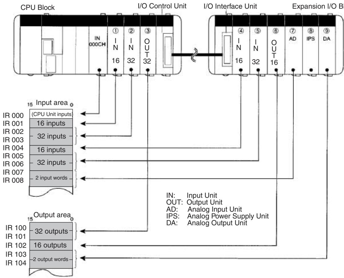
flowchart
graph TD
    subgraph CPU Block
        A["CPU Block"] --> B["Control Unit"]
        B --> C["Interface Unit"]
    end

    subgraph I/O Control Unit
        D["I/O Control Unit"] --> E["Interface Unit"]
        E --> F["Expansion I/O Block"]

    subgraph Input Area
        G["IR 000 (CPU Unit inputs)"] --> H["16 inputs"]
        I["IR 001"] --> J["32 inputs"]
        K["IR 002"] --> L["16 inputs"]
        M["IR 003"] --> N["32 inputs"]
        O["IR 004"] --> P["2 input words"]
    end

    subgraph Output Area
        Q["IR 100 (32 outputs)"] --> R["Output Area"]
        S["IR 101"] --> T["Output Area"]
        U["IR 102"] --> V["Output Area"]
        W["IR 103"] --> X["Output Area"]
        Y["IR 104"] --> Z["Output Area"]
    end

    style CPU Block fill:#f9f,stroke:#333
    style I/O Control Unit fill:#ccf,stroke:#333
    style Expansion I/O Block fill:#cfc,stroke:#333
| Order in PC | Unit | Specifications | Number of words | Allocated word(s) |
| - | CPU Unit | 16 inputs | 1 input word | IR 000 |
| 1 | CQM1-ID111 | 16 inputs | 1 input word | IR 001 |
| 2 | CQM1-ID112 | 32 inputs | 2 input words | IR 002 and IR 003 |
| 3 | CQM1-OD213 | 32 outputs | 2 output words | IR 100 and IR 101 |
| 4 | CQM1-ID111 | 16 inputs | 1 input word | IR 004 |
| 5 | CQM1-ID112 | 32 inputs | 2 input words | IR 005 and IR 006 |
| 6 | CQM1-OC222 | 16 outputs | 1 output word | IR 102 |
| 7 | CQM1-AD041 | 2 input words | 2 input words | IR 007 and IR 008 |
| 8 | CQM1-IPS01 | --- | --- | --- |
| 9 | CQM1-DA021 | 2 output words | 2 output words | IR 103 and IR 104 |
I/O Capacity and Requirements
Note
- I/O words are not allocated to the I/O Control Unit or I/O Interface Unit.
- I/O words are not allocated to the Analog Power Supply Unit, but it is counted as one of the mounted Units.
The number of I/O bits that can be allocated depends on the CQM1H CPU Unit being used, as shown in the following table. Be sure to take into account the one input word (IR 000) that is automatically allocated to inputs on the CPU Unit. If the number of words allocated exceeds the capacity of the CPU Unit, a fatal I/O UNIT OVER error (error code E1) will occur.
| CPU Unit | Max. number of I/O bits | Number of I/O words available to Units other than the CPU Unit |
| CQM1H-CPU61 | 512 bits (256 inputs and 256 outputs) | 31 (15 input words, 16 output words) |
| CQM1H-CPU51 | (32 words: 16 input and 16 output words) | |
| CQM1H-CPU21 | 256 bits | 15 |
| CQM1H-CPU11 |
Refer to page 153 for a table showing how many I/O words are required by each I/O Unit and page 154 for a table showing how many I/O words are required by each Dedicated I/O Unit.
AR 22 indicates the number of input words and output words that have been allocated, as shown in the following diagram.
| Word | Bits | Function | Data range |
| AR 22 | 00 to 07 | The number of input words that have been allocated. | 01 to 16 (2-digit BCD) |
| 08 to 15 | The number of output words that have been allocated. | 00 to 16 (2-digit BCD) |
The CQM1H does not have a Backplane, so it isn't necessary to deal with empty slots when allocating I/O words. The lowest available I/O word addresses are allocated automatically.
Inputs are automatically allocated to input words and outputs are automatically allocated to output words regardless of the order in which the Input Units and Output Units are mounted. Even though I/O allocation is not affected, it is recommended that the Input Units be mounted together and Output Units be mounted together to make the word allocation easier to understand and help eliminate problems with noise.
I/O Words Required by I/O Units
| Name | I/O points | Model | Input words (starting from IR 001) | Output words (starting from IR 100) |
| DC Input Units | 8 | CQM1-ID211 | 1 | --- |
| 16 | CQM1-ID111 | 1 | ||
| CQM1-ID212 | 1 | |||
| 32 | CQM1-ID112 | 2 | ||
| CQM1-ID213 | 2 | |||
| CQM1-ID214 | 2 | |||
| AC Input Units | 8 | CQM1-IA121 | 1 | |
| CQM1-IA221 | 1 | |||
| Relay Output Units | 8 | CQM1-OC221 | --- | 1 |
| 16 | CQM1-OC222 | 1 | ||
| CQM1-OC224 | 1 | |||
| Transistor Output Units | 8 | CQM1-OD211 | 1 | |
| 16 | CQM1-OD212 | 1 | ||
| 32 | CQM1-OD213 | 2 | ||
| CQM1-OD216 | 2 | |||
| 16 | CQM1-OD214 | 1 | ||
| 8 | CQM1-OD215 | 1 | ||
| AC Output Units | 8 | CQM1-OA221 | 1 | |
| 6 | CQM1-OA222 | 1 |
I/O Words Required by Dedicated I/O Units
| Name | Model | Input words (starting from IR 001) | Output words (starting from IR 100) | |
| Analog Input Unit | CQM1-AD041 | 2 or 4 | --- | |
| Analog Output Units | CQM1-DA021 | --- | 2 | |
| CQM1-IPS01 | --- | --- | ||
| CQM1-IPS02 | ||||
| B7A Interface Units | CQM1-B7A02 | --- | 1 | |
| CQM1-B7A12 | 1 | --- | ||
| CQM1-B7A03 | --- | 2 | ||
| CQM1-B7A13 | 2 | --- | ||
| CQM1-B7A21 | 1 | 1 | ||
| G730 Interface Units | CQM1-G7M21 | 2 or 1 | 2 or 1 | |
| CQM1-G7N11 | 2 or 1 | --- | ||
| CQM1-G7N01 | --- | 2 or 1 | ||
| I/O Link Unit | CQM1-LK501 | 2 | 2 | |
| Sensor Units | CQM1-SEN01 | 1 (See note.) | --- | |
| Optical Fiber Photoelectric Module | E3X-MA11 | 1 | ||
| Photoelectric Module with Separate Amplifier | E3C-MA11 | 1 | ||
| Proximity Module with Separate Amplifier | E2C-MA11 | 1 | ||
| Dummy Module | E39-M11 | 1 | ||
| Remote Console | CQM1-TU001 | --- | ||
| Temperature Control Units | CQM1-TC001 | 2 or 1 | 2 or 1 | |
| CQM1-TC002 | ||||
| CQM1-TC101 | ||||
| CQM1-TC102 | ||||
| CQM1-TC201 | 1 | 1 | ||
| CQM1-TC202 | 1 | 1 | ||
| CQM1-TC203 | 1 | 1 | ||
| CQM1-TC204 | 1 | 1 | ||
| CQM1-TC301 | 1 | 1 | ||
| CQM1-TC302 | 1 | 1 | ||
| CQM1-TC303 | 1 | 1 | ||
| CQM1-TC304 | 1 | 1 | ||
| Linear Sensor Interface Units | CQM1-LSE01 | 1 | 1 | |
| CQM1-LSE02 | 1 | 1 | ||
| CompoBus/S Master Unit | CQM1-SRM21-V1 | 4, 2, or 1 | 4, 2, or 1 | |
| CompoBus/D I/O Link Unit | CQM1-DRT21 | 1 | 1 | |
Note A total of 5 words are required when the next 4 Modules (E3X-MA11, E3C-MA11, E2C-MA11, and E39-M11) are mounted.
3-2-4 Flags/Bits for an Inner Board in Slot 1 (IR 200 to IR 215)
Note When using an Inner Board or Communications Unit, do not write to the read bits/words (R) specified in the Read/Write column of the following tables. Writing to these bits/words may produce unexpected results.
Note Applicable only for CQM1H-SCB41, lot numbers 0320 or later.
Serial Communications Board Flags/Bits
| Word | Bits | Function | Read/Write | Communications modes | |
| IR 200 | 00 | Serial Communications Board Hardware Error Flag | R | All modes | |
| 01 | Port Identification Error Flag (hardware error) | R | |||
| 02 | Protocol Data Error Flag | R | Protocol macro | ||
| 03 to 10 | Not used. | R | |||
| 11 | Port 2 Protocol Macro Execution Error Flag | R | |||
| 12 | Port 1 Protocol Macro Execution Error Flag | R | |||
| 13 | Port 2 PC Setup Error Flag | R | All modes | ||
| 14 | Port 1 PC Setup Error Flag | R | |||
| 15 | PC Setup Error Flag | R | |||
| IR 201 | 00 to 03 | Port 1 | Error Code0: Normal operation 1: Parity error 2: Framing error3: Overrun error 4: FCS error 5: Timeout error6: Checksum error 7: Command error | R | All modes |
| 04 | Communications Error Flag | R | |||
| 05 | Transmission Enabled Flag | R | Host Link or No-protocol | ||
| 06 | Reception Completed Flag | R | |||
| 07 | Reception Overflow Flag | R | |||
| Sequence Abort Completion Flag | R | Protocol macro | |||
| 08 to 11 | Port 2 | Error Code0: Normal operation 1: Parity error 2: Framing error3: Overrun error 4: FCS error 5: Timeout error6: Checksum error 7: Command error | R | All modes | |
| 12 | Communications Error Flag | R | |||
| 13 | Transmission Enabled Flag | R | Host Link or No-protocol | ||
| 14 | Reception Completed Flag | R | |||
| 15 | Reception Overflow Flag | R | |||
| Sequence Abort Completion Flag | R | Protocol macro | |||
| IR 202 | 00 to 07 | Port 1 | Communicating with PT Flags (Bits 00 to 07 = PTs 0 to 7) | R | NT Link in 1:N mode |
| Repeat Counter PV (00 to FF hexadecimal) | R | Protocol macro | |||
| 00 to 15 | Reception Counter (4-digit BCD) | R | No-protocol | ||
| IR 203 | 00 to 07 | Port 2 | Communicating with PT Flags (Bits 00 to 07 = PTs 0 to 7) | R | NT Link in 1:N mode |
| Repeat Counter PV (00 to FF hexadecimal) | R | Protocol macro | |||
| 00 to 15 | Reception Counter (4-digit BCD) | R | No-protocol | ||
| IR 204 | 00 | Port 1 | Tracing Flag | R | Protocol macro |
| 01 | Port 2 | R | |||
| 02 to 05 | Not used. | R | |||
| 06 | Port 1 | Echoback Disabled Flag (Only used for modem control in pro-tocol macro mode. See note.) | R | ||
| 07 | Port 2 | R | |||
| 08 to 11 | Port 1 | Protocol Macro Error Code0: Normal operation 1: No protocol macro function2: Sequence number error 3: Reception data/write area overflow4: Protocol data grammar error | R | Protocol macro | |
| 12 to 15 | Port 2 | R | |||
| IR 205 | 00 to 03 | Port 1 | Completed Reception Case Number | R | Protocol macro |
| 04 to 07 | Completed Step Number | R | |||
| 08 to 14 | Not used. | R | |||
| 15 | IR 20408 to IR 20411 Data Stored Flag0: No data stored; 1: Data stored | R | |||
| IR 206 | 00 to 03 | Port 2 | Completed Reception Case Number | R | Protocol macro |
| 04 to 07 | Completed Step Number | R | |||
| 08 to 14 | Not used. | R | |||
| 15 | IR 20412 to IR 20415 Data Stored Flag0: No data stored; 1: Data stored | R | |||
| IR 207 | 00 | Port 1 | Serial Communications Port Restart Bits | W | All modes |
| 01 | Port 2 | ||||
| 02 | Port 1 | Continuous Trace Start/Stop Bits | W | Protocol macro | |
| 03 | Port 2 | ||||
| 04 | Port 1 | Shot Trace Start/Stop Bits | W | ||
| 05 | Port 2 | ||||
| 06 | Port 1 | Echoback Disable Bit (Only used for modem control in protocol macro mode. See note.) | W | ||
| 07 | Port 2 | ||||
| 08 | Port 1 | Protocol Macro Executing Flag | R | No-protocol or Protocol macro | |
| 09 | Step Error Processing Flag | R | Protocol macro | ||
| 10 | Sequence End Completion Flag | R | |||
| 11 | Forced Abort Bit | W | |||
| 12 | Port 2 | Protocol Macro Executing Flag | R | No-protocol or Protocol macro | |
| 13 | Step Error Processing Flag | R | Protocol macro | ||
| 14 | Sequence End Completion Flag | R | |||
| 15 | Forced Abort Bit | W | |||
| IR 208 to IR 215 | 00 to 15 | Not used. | --- | --- | |
High-speed Counter Board Flags/Bits
| Word | Bits | Name | Function | Read/Write | |
| IR 200 | 00 to 15 | High-speed Counter 1 | PV (rightmost 4 digits) | Contains the high-speed counter PV for each of the High-speed Counter Board's ports. Note The PV data format (BCD or hexa-decimal) can be set in the PC Setup (DM 6602.) | R |
| IR 201 | 00 to 15 | PV (leftmost 4 digits) | |||
| IR 202 | 00 to 15 | High-speed Counter 2 | PV (rightmost 4 digits) | ||
| IR 203 | 00 to 15 | PV (leftmost 4 digits) | |||
| IR 204 | 00 to 15 | High-speed Counter 3 | PV (rightmost 4 digits) | ||
| IR 205 | 00 to 15 | PV (leftmost 4 digits) | |||
| IR 206 | 00 to 15 | High-speed Counter 4 | PV (rightmost 4 digits) | ||
| IR 207 | 00 to 15 | PV (leftmost 4 digits) | |||
| Word | Bits | Name | Function | Read/Write |
| IR 208(High-speed counter 1) | 00 to 07 | Comparison Results: Internal Output Bits | Contains the bit pattern specified by oper-and in CTBL(—) when conditions are satisfied. | R |
| IR 209(High-speed counter 2) | 08 to 11 | Comparison Results: External Output Bits for Outputs 1 to 4 | Contains the bit pattern specified by oper-and in CTBL(—) when conditions are satisfied. | R |
| IR 210(High-speed counter 3) | 12 | Counter Operating Flag | 0: Stopped1: Operating | R |
| 13 | Comparison Flag | Indicates whether comparison is in progress.0: Stopped; 1: Operating | R | |
| IR 211(High-speed counter 4) | 14 | PV Overflow/Underflow Flag | 0: Normal1: Overflow or underflow occurred. | R |
| 15 | SV Error Flag | 0: Normal1: SV error occurred. | R | |
| IR 212 | 00 | High-speed Counter 1 Reset Bit | Phase Z and software reset0: Counter not reset on phase Z1: Counter reset on phase ZSoftware reset only0: Counter not reset0→1: Counter reset | W |
| 01 | High-speed Counter 2 Reset Bit | |||
| 02 | High-speed Counter 3 Reset Bit | |||
| 03 | High-speed Counter 4 Reset Bit | |||
| 04 to 07 | Not used. | --- | ||
| 08 | High-speed Counter 1 Comparison Stop Bit | 0→1: Starts comparison.1→0: Stops comparison. | W | |
| 09 | High-speed Counter 2 Comparison Stop Bit | |||
| 10 | High-speed Counter 3 Comparison Stop Bit | |||
| 11 | High-speed Counter 4 Comparison Stop Bit | |||
| 12 | High-speed Counter 1 Stop Bit | 0: Continues operation.1: Stops operation. | W | |
| 13 | High-speed Counter 2 Stop Bit | |||
| 14 | High-speed Counter 3 Stop Bit | |||
| 15 | High-speed Counter 4 Stop Bit | |||
| IR 213 | 00 | External Output 1 Force-set Bit | 0: No effect on output status1: Forces output ON | W |
| 01 | External Output 2 Force-set Bit | |||
| 02 | External Output 3 Force-set Bit | |||
| 03 | External Output 4 Force-set Bit | |||
| 04 | External Output Force-set Enable Bit | 1: Force-setting of outputs 1 to 4 enabled0: Force-setting of outputs 1 to 4 disabled | W | |
| 05 to 15 | Not used. | --- | ||
Analog Setting Board (Slot 1 and 2) Flags/Bits
| Word | Bits | Function | Read/Write |
| IR 220 | 00 to 15 | Analog SV 1: 0000 to 0200 (4-digit BCD) | R |
| IR 221 | 00 to 15 | Analog SV 2: 0000 to 0200 (4-digit BCD) | R |
| IR 222 | 00 to 15 | Analog SV 3: 0000 to 0200 (4-digit BCD) | R |
| IR 223 | 00 to 15 | Analog SV 4: 0000 to 0200 (4-digit BCD) | R |
3-2-5 Flags/Bits for an Inner Board in Slot 2 (IR 232 to IR 243)
High-speed Counter Board Flags/Bits
| Word | Bits | Name | Function | Read/Write | |
| IR 232 | 00 to 15 | High-speed Counter 1 | PV (rightmost 4 digits) | Contains the high-speed counter PV for each of the High-speed Counter Board's ports. Note The PV data format (BCD or hexa-decimal) can be set in the PC Set-up (DM 6602.) | R |
| IR 233 | 00 to 15 | PV (leftmost 4 digits) | |||
| IR 234 | 00 to 15 | High-speed Counter 2 | PV (rightmost 4 digits) | ||
| IR 235 | 00 to 15 | PV (leftmost 4 digits) | |||
| IR 236 | 00 to 15 | High-speed Counter 3 | PV (rightmost 4 digits) | ||
| IR 237 | 00 to 15 | PV (leftmost 4 digits) | |||
| IR 238 | 00 to 15 | High-speed Counter 4 | PV (rightmost 4 digits) | ||
| IR 239 | 00 to 15 | PV (leftmost 4 digits) | |||
| IR 240(High-speed counter 1) | 00 to 07 | Comparison Results: Internal Output Bits | Contains the bit pattern specified by oper-and in CTBL(—) when conditions are sat-isfied. | R | |
| IR 241(High-speed counter 2) | 08 to 11 | Comparison Results: External Outputs Bits for Outputs 1 to 4 | Contains the bit pattern specified by oper-and in CTBL(—) when conditions are sat-isfied. | R | |
| IR 242(High-speed counter 3) | 12 | Counter Operating Flag | 0: Stopped1: Operating | R | |
| IR 243(High-speed counter 4) | 13 | Comparison Flag | Indicates whether comparison is in progress.0: Stopped; 1: Operating | R | |
| 14 | PV Overflow/Underflow Flag | 0: Normal1: Overflow or underflow occurred. | R | ||
| 15 | SV Error Flag | 0: Normal1: SV error occurred. | R | ||
| AR 05 | 00 | High-speed Counter 1 Reset Bit | Phase Z and software reset0: Phase-Z reset disabled1: Phase-Z reset enabledSoftware reset only0: Software reset disabled0→1: Executes software reset | ||
| 01 | High-speed Counter 2 Reset Bit | ||||
| 02 | High-speed Counter 3 Reset Bit | ||||
| 03 | High-speed Counter 4 Reset Bit | ||||
| 04 to 07 | Not used. | ||||
| 08 | High-speed Counter 1 Comparison Stop Bit | 0→1: Starts comparison.1→0: Stops comparison. | |||
| 09 | High-speed Counter 2 Comparison Stop Bit | ||||
| 10 | High-speed Counter 3 Comparison Stop Bit | ||||
| 11 | High-speed Counter 4 Comparison Stop Bit | ||||
| 12 | High-speed Counter 1 Stop Bit | 0: Continues operation.1: Stops operation. | |||
| 13 | High-speed Counter 2 Stop Bit | ||||
| 14 | High-speed Counter 3 Stop Bit | ||||
| 15 | High-speed Counter 4 Stop Bit | ||||
| AR 06 | 00 | External Output 1 Force-set Bit | 0: No effect on output status1: Forces output ON | ||
| 01 | External Output 2 Force-set Bit | ||||
| 02 | External Output 3 Force-set Bit | ||||
| 03 | External Output 4 Force-set Bit | ||||
| 04 | External Output Force-set Enable Bit | 1: Force-setting of outputs 1 to 4 enabled0: Force-setting of outputs 1 to 4 disabled | |||
| 05 to 15 | Not used. | ||||
Pulse I/O Board Flags/Bits
| Word | Bits | Function | Read/Write |
| IR 232 | 00 to 15 | High-speed Counter 1 PV (rightmost 4 digits) | R |
| IR 233 | 00 to 15 | High-speed Counter 1 PV (leftmost 4 digits) | R |
| IR 234 | 00 to 15 | High-speed Counter 2 PV (rightmost 4 digits) | R |
| IR 235 | 00 to 15 | High-speed Counter 2 PV (leftmost 4 digits) | R |
| IR 236 | 00 to 15 | Port 1 Pulse Output PV (rightmost 4 digits) | R |
| IR 237 | 00 to 15 | Port 1 Pulse Output PV (leftmost 4 digits) | R |
| IR 238 | 00 to 15 | Port 2 Pulse Output PV (rightmost 4 digits) | R |
| IR 239 | 00 to 15 | Port 2 Pulse Output PV (leftmost 4 digits) | R |
| IR 240 to IR 243 | 00 to 15 | Not used. | --- |
Absolute Encoder Interface Board Flags/Bits
| Word | Bits | Function | Read/Write |
| IR 232 | 00 to 15 | Absolute Encoder High-speed Counter 1 PV (rightmost 4 digits) | R |
| IR 233 | 00 to 15 | Absolute Encoder High-speed Counter 1 PV (leftmost 4 digits) | R |
| IR 234 | 00 to 15 | Absolute Encoder High-speed Counter 2 PV (rightmost 4 digits) | R |
| IR 235 | 00 to 15 | Absolute Encoder High-speed Counter 2 PV (leftmost 4 digits) | R |
| IR 236 to IR 243 | 00 to 15 | Not used. | --- |
Analog I/O Board Flags/Bits
| Word | Bits | Function | Read/Write |
| IR 232 | 00 to 15 | Analog Input 1 Conversion Value | R |
| IR 233 | 00 to 15 | Analog Input 2 Conversion Value | R |
| IR 234 | 00 to 15 | Analog Input 3 Conversion Value | R |
| IR 235 | 00 to 15 | Analog Input 4 Conversion Value | R |
| IR 236 | 00 to 15 | Analog Output 1 SV | W |
| IR 237 | 00 to 15 | Analog Output 2 SV | W |
| IR 238 to IR 243 | 00 to 15 | Not used. | --- |
Analog Setting Board (Slot 1 and 2) Flags/Bits
| Word | Bits | Function | Read/Write |
| IR 220 | 00 to 15 | Analog SV 1: 0000 to 0200 (4-digit BCD) | R |
| IR 221 | 00 to 15 | Analog SV 2: 0000 to 0200 (4-digit BCD) | R |
| IR 222 | 00 to 15 | Analog SV 3: 0000 to 0200 (4-digit BCD) | R |
| IR 223 | 00 to 15 | Analog SV 4: 0000 to 0200 (4-digit BCD) | R |
3-2-6 Flags/Bits for Communications Units
Controller Link Status Area 1 (IR 090 to IR 095)
| Word | Bits | Function |
| IR 090 | 00 to 14 | Always 0 |
| 15 | Local Node's Data Link Participation Status0: The local node not in the Data Link or Data Link is stopped.1: The local node is participating in the Data Link. | |
| IR 091 | 00 to 07 | Data Link Status: Node 1 |
| 08 to 15 | Data Link Status: Node 2 | |
| IR 092 | 00 to 07 | Data Link Status: Node 3 |
| 08 to 15 | Data Link Status: Node 4 | |
| IR 093 | 00 to 07 | Data Link Status: Node 5 |
| 08 to 15 | Data Link Status: Node 6 |
Controller Link Status Area 2 (IR 190 to IR 195)
| Word | Bits | Function |
| IR 094 | 00 to 15 | Not used. |
| IR 095 | 00 to 10 | Always 0 |
| 11 | Terminator Status0: Terminating resistance switch OFF1: Terminating resistance switch ON | |
| 12 to 15 | Always 0 |
| Word | Bits | Function |
| IR 190 | 00 | Network Parameters Error Flag1: Error occurred; 0: No error |
| 01 | Data Link Table Error Flag1: Error occurred; 0: No error | |
| 02 | Routing Table Error Flag1: Error occurred; 0: No error | |
| 03 to 06 | Always 0 | |
| 07 | EEPROM Write Error Flag1: Error occurred; 0: No error | |
| 08 | Always 0 | |
| 09 | Node Number Duplication Error Flag1: Error occurred; 0: No error | |
| 10 | Network Parameters Mismatch Error Flag1: Error occurred; 0: No error | |
| 11 | Communications Controller Transmitter Error Flag1: Error occurred; 0: No error | |
| 12 | Communications Controller Hardware Error Flag1: Error occurred; 0: No error | |
| 13 and 14 | Always 0 | |
| 15 | Error Log Flag1: Error record recorded; 0: No error records recorded | |
| IR 191 | 00 to 07 | Polling Node's Node Number |
| 08 to 15 | Startup Node's Node Number | |
| IR 192 and IR 193 | 00 to 15 | Network Participation Status1: Participating in network; 0: Not participating in network |
| IR 194 and IR 195 | 00 to 15 | Not used. |
3-3 SR Area
These bits mainly serve as flags related to CQM1H operation. The following table provides details on the various bit functions.
SR 244 to SR 247 can also be used as work bits when input interrupts are not used in Counter Mode.
| Word | Bit(s) | Function | Page |
| SR244 | 00 to 15 | Input Interrupt 0 Counter Mode SVSV when input interrupt 0 is used in Counter Mode (4-digit hexadecimal, 0000 to FFFF). (Can be used as work bits when input interrupt 0 is not used in Counter Mode.) | 28 |
| SR245 | 00 to 15 | Input Interrupt 1 Counter Mode SVSV when input interrupt 1 is used in Counter Mode (4-digit hexadecimal, 0000 to FFFF). (Can be used as work bits when input interrupt 1 is not used in Counter Mode.) | |
| SR246 | 00 to 15 | Input Interrupt 2 Counter Mode SVSV when input interrupt 2 is used in Counter Mode (4-digit hexadecimal, 0000 to FFFF). (Can be used as work bits when input interrupt 2 is not used in Counter Mode.) | |
| SR247 | 00 to 15 | Input Interrupt 3 Counter Mode SVSV when input interrupt 3 is used in Counter Mode (4-digit hexadecimal, 0000 to FFFF). (Can be used as work bits when input interrupt 3 is not used in Counter Mode.) | |
| SR248 | 00 to 15 | Input Interrupt 0 Counter Mode PV Minus OneCounter PV-1 when input interrupt 0 is used in Counter Mode (4-digit hexadecimal). | 28 |
| SR249 | 00 to 15 | Input Interrupt 1 Counter Mode PV Minus OneCounter PV-1 when input interrupt 1 is used in Counter Mode (4-digit hexadecimal). | |
| SR250 | 00 to 15 | Input Interrupt 2 Counter Mode PV Minus OneCounter PV-1 when input interrupt 2 is used in Counter Mode (4-digit hexadecimal). | |
| SR251 | 00 to 15 | Input Interrupt 3 Counter Mode PV Minus OneCounter PV-1 when input interrupt 3 is used in Counter Mode (4-digit hexadecimal). | |
| SR252 | 00 | High-speed Counter 0 Reset Bit | 35 |
| 01 | Control Bit for Inner Board in Slot 2Pulse I/O Board: High-speed Counter 1 Reset BitTurn ON to reset PV of high-speed counter 1 (port 1).Absolute Encoder Interface Board:Absolute High-speed Counter 1 Origin Compensation BitTurn ON to set origin compensation for absolute high-speed counter 1 (port 1). Automatically turns OFF when compensation value is set in DM 6611. | 147 | |
| 02 | Control Bit for Inner Board in Slot 2Pulse I/O Board: High-speed Counter 2 Reset BitTurn ON to reset PV of high-speed counter 2 (port 2).Absolute Encoder Interface Board:Absolute High-speed Counter 2 Origin Compensation BitTurn ON to set origin compensation for absolute high-speed counter 2 (port 2). Automatically turns OFF when compensation value is set in DM 6612. | 147 | |
| 03 to 07 | Not used. | ||
| 08 | Peripheral Port Reset BitTurn ON to reset peripheral port. (Not valid when Programming Device is connected.)Automatically turns OFF when reset is complete. | 52 | |
| 09 | RS-232C Port Reset BitTurn ON to reset RS-232C port. Automatically turns OFF when reset is complete. | ||
| 10 | PC Setup Reset BitTurn ON to initialize PC Setup (DM 6600 through DM 6655). Automatically turns OFF again when reset is complete. Only effective if the PC is in PROGRAM mode. | 2 | |
| 11 | Forced Status Hold BitOFF: Bits that are forced set/reset are cleared when switching from PROGRAM mode to MONITOR mode.ON: The status of bits that are forced set/reset are maintained when switching from PROGRAM mode to MONITOR mode. | 13 | |
| 12 | I/O Hold BitOFF: IR and LR bits are reset when starting or stopping operation.ON: IR and LR bit status is maintained when starting or stopping operation. | 13 | |
| 13 | Not used. | ||
| 14 | Error Log Reset BitTurn ON to clear error log. Automatically turns OFF again when operation is complete. | 505 | |
| 15 | Output OFF BitOFF: Normal output status.ON: All outputs turned OFF. | 163 | |
| SR253 | 00 to 07 | FAL Error CodeThe error code (a 2-digit number) is stored here when an error occurs. The FAL number is stored here when FAL(06) or FALS(07) is executed. This byte is reset (to 00) by executing a FAL 00 instruction or by clearing the error from a Programming Device. | 230 |
| 08 | Low Battery FlagTurns ON when a CPU Unit battery voltage drops. | 502 | |
| 09 | Cycle Time Over FlagTurns ON when a cycle time overrun occurs (i.e., when cycle time exceeds 100 ms). | 502 | |
| 10 to 12 | Not used. | ||
| 13 | Always ON Flag | --- | |
| 14 | Always OFF Flag | --- | |
| SR253 | 15 | First Cycle FlagTurns ON for 1 cycle at the start of operation. | --- |
| SR254 | 00 | 1-minute Clock Pulse (30 seconds ON; 30 seconds OFF) | --- |
| 01 | 0.02-second Clock Pulse (0.01 second ON; 0.01 second OFF) | --- | |
| 02 to 03 | Not used. | ||
| 04 | Overflow (OF) FlagTurns ON when the result of a calculation is above the upper limit of signed binary data. | 328 | |
| 05 | Underflow (UF) FlagTurns ON when the result of a calculation is below the lower limit of signed binary data. | 328 | |
| 06 | Differential Monitor Complete FlagTurns ON when differential monitoring is complete. | 147 | |
| 07 | STEP(08) Execution FlagTurns ON for 1 cycle only at the start of process based on STEP(08). | 231 | |
| 08 | HKY(—) Execution FlagTurns ON during execution of HKY(—). | 431 | |
| 09 | 7SEG(88) Execution FlagTurns ON during execution of 7SEG(88). | 424 | |
| 10 | DSW(87) Execution FlagTurns ON during execution of DSW(87). | 427 | |
| 11 to 12 | Not used. | ||
| 13 | Communications Unit Error FlagTurns ON when an error occurs in a Communications Unit. This flag mirrors the operation of the Communications Unit Error Flag (AR 0011). | 427 | |
| 14 | Not used. | ||
| 15 | Inner Board Error FlagTurns ON when an error occurs in an Inner Board mounted in slot 1 or slot 2. The error code for slot 1 is stored in AR 0400 to AR 0407 and the error code for slot 2 is stored in AR 0408 to AR 0415. | --- | |
| SR255 | 00 | 0.1-second Clock Pulse (0.05 second ON; 0.05 second OFF) | --- |
| 01 | 0.2-second Clock Pulse (0.1 second ON; 0.1 second OFF) | --- | |
| 02 | 1.0-second Clock Pulse (0.5 second ON; 0.5 second OFF) | --- | |
| 03 | Instruction Execution Error (ER) FlagTurns ON when an error occurs during execution of an instruction. | --- | |
| 04 | Carry (CY) FlagTurns ON when there is a carry in the results of an instruction execution. | --- | |
| 05 | Greater Than (GR) FlagTurns ON when the result of a comparison operation is “greater.” | --- | |
| 06 | Equals (EQ) FlagTurns ON when the result of a comparison operation is “equal,” or when the result of an instruction execution is 0. | --- | |
| 07 | Less Than (LE) FlagTurns ON when the result of a comparison operation is “less.” | --- | |
SR 25211
(Forced Status Hold Bit)
When the forced set/reset status is cleared, the bits that were forced will be turned ON or OFF as follows:
Forced set cleared: Bit turned ON
Forced reset cleared: Bit turned OFF
All force-set or force-reset bits will be cleared when the PC is switched to RUN mode unless DM 6601 in the PC Setup has been set to maintain the previous status of the Forced Status Hold Bit when power is turned ON. This setting can be used to prevent forced status from being cleared even when power is turned ON.
Turn this bit ON and OFF from a Programming Device.
SR 25212
(I/O Hold Bit)
When this bit is ON, the status of bits in the IR and LR areas will be retained when the PC is switched from PROGRAM to RUN or MONITOR mode. (If the
SR 25215 (Output OFF Bit)
I/O Hold Bit is OFF, all IR and LR bits will be reset when the PC starts operation.)
Turn this bit ON and OFF from a Programming Device.
DM 6601 in the PC Setup can be set to maintain the previous status of the I/O Hold Bit when power is turned ON. When this setting has been made and the I/O Hold BIt is ON, the status of bits in the IR and LR areas will not be cleared when the power is turned ON.
When this bit is turned ON, all outputs will be turned OFF and the CPU Unit's INH indicator will light. As long as the Output OFF BIt is ON, outputs will remain OFF even if output bits are turned ON by the program.
Pulse outputs from Transistor Output Units and Pulse I/O Boards will remain OFF as long as the Output OFF Bit is ON. If a High-speed Counter Board has been installed, the Board's external outputs (1 to 4) will remain OFF as long as the Output OFF Bit is ON.
When the Output OFF Bit will normally be OFF, turn it OFF regularly from the program. If the Output OFF BIt is not turned OFF from the program, its ON/OFF status will be retained when the power is OFF (although its status may not be retained if the backup battery fails.)
SR 25308 (Battery Low Flag)
A setting can be made in the PC Setup (DM 6655) so that these errors will not be generated.
SR 25309 (Cycle Time Over Flag)
A setting can be made in the PC Setup (DM 6655) so that these errors will not be generated.
3-4 TR Area
When a complex ladder diagram cannot be programmed in mnemonic code just as it is, these bits are used to temporarily store ON/OFF execution conditions at program branches. They are used only for mnemonic code. When programming directly with ladder diagrams, TR bits are automatically processed for you.
The same TR bits cannot be used more than once within the same instruction block, but can be used again in different instruction blocks. The ON/OFF status of TR bits cannot be monitored from a Programming Device.
Examples showing the use of TR bits in programming are provided on page 195.
3-5 HR Area
These bits retain their ON/OFF status even after the CQM1H power supply has been turned OFF or when operation begins or stops. They are used in the same way as work bits.
Caution
Never use an input bit in a NC condition on the reset (R) for KEEP(11) when the input device uses an AC power supply (see diagram below). The delay in shutting down the PC's DC power supply relative to the AC power supply to the input device can cause the designate bit of KEEP(11) to be reset.
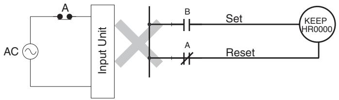
3-6 AR Area
These bits mainly serve as flags related to CQM1H operation. The flags in AR 05 and AR 06 relate to the operation of Inner Boards and their functions are different for each Inner Board. The following table has been split to show the functions of the shared flags (AR 00 to AR 04 and AR 07 to AR 27) and the flags unique to particular Inner Boards (AR 05 and AR 06.)
With the exception of AR 23 (Power-off Counter), the status of AR words and bits is refreshed each cycle. (AR 23 is refreshed only for power interruptions.)
3-6-1 Shared Flags/Bits (AR 00 to AR 04)
| Word | Bit(s) | Function |
| AR 00 | 00 to 10 | Not used. |
| 11 | Communications Unit Error FlagTurns ON when an error occurs in a Communications Unit. | |
| 12 to 15 | Not used. | |
| AR 01 | 00 to 10 | Not used. |
| 11 | Communications Unit Restart BitTurn this bit ON and then OFF to restart the Communications Unit. | |
| 12 to 15 | Not used. | |
| AR 02 | 00 to 07 | Network Instruction Completion CodeContains the completion code for network instructions (SEND(90), RECV(98), or CMND(—).) |
| 08 | Network Instruction (SEND(90), RECV(98), or CMND(—)) Error FlagTurns ON when an error occurred in execution of a network instruction (SEND(90), RECV(98), or CMND(—).) | |
| 09 | Network Instruction (SEND(90), RECV(98), or CMND(—)) Enabled FlagTurns ON when a network instruction (SEND(90), RECV(98), or CMND(—)) can be executed. | |
| 10 to 14 | Not used. | |
| 15 | Communications Unit Connected FlagTurns ON when a Communications Unit is mounted to the PC. | |
| AR 03 | 00 to 15 | Communications Unit Servicing TimeIndicates the servicing time for the last cycle in 0.1-ms units (4-digit BCD.) |
| AR 04 | 00 to 07 | Slot 1 Inner Board Error Code (Hex)00: Normal01, 02: Hardware error04: Serial Communications Board error |
| 08 to 15 | Slot 2 Inner Board Error Code (Hex)00: Normal01, 02: Hardware error03: PC Setup error04: PC stopped during pulse output or A/D (D/A) conversion error |
3-6-2 Flags/Bits for Inner Boards (AR 05 and AR 06)
High-speed Counter Board Slot 2 Flags/Bits (AR 05 to AR 06)
| Word | Bit(s) | Function | Operation |
| AR 05 | 00 | High-speed Counter 1 Reset Bit | Z Phase and software reset0: Z-phase reset disabled1: Z-phase reset enabledSoftware reset only0: Software reset disabled0→1: Executes software reset |
| 01 | High-speed Counter 2 Reset Bit | ||
| 02 | High-speed Counter 3 Reset Bit | ||
| 03 | High-speed Counter 4 Reset Bit | ||
| 04 to 07 | Not used. | --- | |
| 08 | High-speed Counter 1 Comparison Stop Bit | 0→1: Starts comparison.1→0: Stops comparison. | |
| 09 | High-speed Counter 2 Comparison Stop Bit | ||
| 10 | High-speed Counter 3 Comparison Stop Bit | ||
| 11 | High-speed Counter 4 Comparison Stop Bit | ||
| 12 | High-speed Counter 1 Stop Bit | 0: Continues operation.1: Stops operation. | |
| 13 | High-speed Counter 2 Stop Bit | ||
| 14 | High-speed Counter 3 Stop Bit | ||
| 15 | High-speed Counter 4 Stop Bit | ||
| AR 06 | 00 | External Output 1 Force-set Bit | 0: Not valid1: Forced ON |
| 01 | External Output 2 Force-set Bit | ||
| 02 | External Output 3 Force-set Bit | ||
| 03 | External Output 4 Force-set Bit | ||
| 04 | External Output Force-set Enable Bit | 0: Force-setting of outputs 1 to 4 disabled1: Force-setting of outputs 1 to 4 enabled | |
| 05 to 15 | Not used. | --- |
Pulse I/O Board Slot 2 Flags/Bits (AR 05 to AR 06)
| Word | Bit(s) | Operation |
| AR 05 | 00 to 07 | High-speed Counter 1 Range Comparison FlagsBit 00 ON: Counter PV satisfies conditions for comparison range 1Bit 01 ON: Counter PV satisfies conditions for comparison range 2Bit 02 ON: Counter PV satisfies conditions for comparison range 3Bit 03 ON: Counter PV satisfies conditions for comparison range 4Bit 04 ON: Counter PV satisfies conditions for comparison range 5Bit 05 ON: Counter PV satisfies conditions for comparison range 6Bit 06 ON: Counter PV satisfies conditions for comparison range 7Bit 07 ON: Counter PV satisfies conditions for comparison range 8 |
| 08 | High-speed Counter 1 Comparison FlagOFF: StoppedON: Comparing | |
| 09 | High-speed Counter 1 Overflow/Underflow FlagOFF: NormalON: Overflow or underflow occurred. | |
| 10 to 11 | Not used. | |
| 12 to 15 | Port 1 Pulse Output FlagsBit 12 ON: Deceleration specified. (OFF: Not specified.)Bit 13 ON: Number of pulses specified. (OFF: Not specified.)Bit 14 ON: Pulse output completed. (OFF: Not completed.)Bit 15 ON: Pulse output in progress. (OFF: No pulse output.) | |
| AR 06 | 00 to 07 | High-speed Counter 2 Range Comparison FlagsBit 00 ON: Counter PV satisfies conditions for comparison range 1Bit 01 ON: Counter PV satisfies conditions for comparison range 2Bit 02 ON: Counter PV satisfies conditions for comparison range 3Bit 03 ON: Counter PV satisfies conditions for comparison range 4Bit 04 ON: Counter PV satisfies conditions for comparison range 5Bit 05 ON: Counter PV satisfies conditions for comparison range 6Bit 06 ON: Counter PV satisfies conditions for comparison range 7Bit 07 ON: Counter PV satisfies conditions for comparison range 8 |
| 08 | High-speed Counter 2 Comparison FlagOFF: StoppedON: Comparing | |
| 09 | High-speed Counter 2 Overflow/Underflow FlagOFF: NormalON: Overflow or underflow occurred. | |
| 10 to 11 | Not used. | |
| 12 to 15 | Port 2 Pulse Output FlagsBit 12 ON: Deceleration specified. (OFF: Not specified.)Bit 13 ON: Number of pulses specified. (OFF: Not specified.)Bit 14 ON: Pulse output completed. (OFF: Not completed.)Bit 15 ON: Pulse output in progress. (OFF: No pulse output.) |
Absolute Encoder Interface Board Flags/Bits (AR 05 to AR 06)
| Word | Bit(s) | Operation |
| AR 05 | 00 to 07 | High-speed Counter 1 Range Comparison FlagsBit 00 ON: Counter PV satisfies conditions for comparison range 1Bit 01 ON: Counter PV satisfies conditions for comparison range 2Bit 02 ON: Counter PV satisfies conditions for comparison range 3Bit 03 ON: Counter PV satisfies conditions for comparison range 4Bit 04 ON: Counter PV satisfies conditions for comparison range 5Bit 05 ON: Counter PV satisfies conditions for comparison range 6Bit 06 ON: Counter PV satisfies conditions for comparison range 7Bit 07 ON: Counter PV satisfies conditions for comparison range 8 |
| 08 | High-speed Counter 1 Comparison FlagOFF: StoppedON: Comparing | |
| 09 to 15 | Not used. | |
| AR 06 | 00 to 07 | High-speed Counter 2 Range Comparison FlagsBit 00 ON: Counter PV satisfies conditions for comparison range 1Bit 01 ON: Counter PV satisfies conditions for comparison range 2Bit 02 ON: Counter PV satisfies conditions for comparison range 3Bit 03 ON: Counter PV satisfies conditions for comparison range 4Bit 04 ON: Counter PV satisfies conditions for comparison range 5Bit 05 ON: Counter PV satisfies conditions for comparison range 6Bit 06 ON: counter PV satisfies conditions for comparison range 7Bit 07 ON: Counter PV satisfies conditions for comparison range 8 |
| 08 | High-speed Counter 2 Comparison FlagOFF: StoppedON: Comparing | |
| 09 to 15 | Not used. |
3-6-3 Shared Flags/Bits (AR 07 to AR 27)
| Word | Bit(s) | Function |
| AR 07 | 00 | Controller Link Data Link Start BitOFF→ON: Start (This bit is ON when the power is turned ON.)ON→OFF: Stop |
| 01 to 11 | Not used. | |
| 12 | DIP Switch Pin 6 FlagOFF: CPU Unit's DIP switch pin No. 6 is OFF.ON: CPU Unit's DIP switch pin No. 6 is ON. | |
| 13 to 15 | Not used. | |
| AR 08 | 00 to 03 | RS-232C Port Error Code (1-digit number)0: Normal completion; 1: Parity error; 2: Framing error; 3: Overrun error |
| 04 | RS-232C Port Error FlagTurns ON when a communications error occurs at the CPU Unit's built-in RS-232C port. | |
| 05 | RS-232C Port Transmission Enabled FlagValid only when host link or RS-232C communications are used at the CPU Unit's built-in RS-232C port. | |
| 06 | RS-232C Port Reception Completed FlagValid only when RS-232C communications are used at the CPU Unit's built-in RS-232C port. | |
| 07 | RS-232C Port Reception Overflow FlagValid only when host link or RS-232C communications are used at the CPU Unit's built-in RS-232C port. | |
| 08 to 11 | Peripheral Port Error Code (1-digit number)0: Normal completion; 1: Parity error; 2: Framing error; 3: Overrun error | |
| 12 | Peripheral Port Error FlagTurns ON when a peripheral port communications error occurs. | |
| 13 | Peripheral Port Transmission Enabled FlagValid only when host link or RS-232C communications are used. | |
| 14 | Peripheral Port Reception Completed FlagValid only when RS-232C communications are used. | |
| 15 | Peripheral Port Reception Overflow FlagValid only when host link or RS-232C communications are used. | |
| AR 09 | 00 to 15 | RS-232C Port Reception Counter4 digits BCD; valid only when RS-232C communications are used. |
| AR 10 | 00 to 15 | Peripheral Port Reception Counter4 digits BCD; valid only when RS-232C communications are used. |
| AR 11 | 00 to 07 | High-speed Counter 0 Range Comparison FlagsBit 00 ON: Counter PV satisfies conditions for comparison range 1Bit 01 ON: Counter PV satisfies conditions for comparison range 2Bit 02 ON: Counter PV satisfies conditions for comparison range 3Bit 03 ON: Counter PV satisfies conditions for comparison range 4Bit 04 ON: Counter PV satisfies conditions for comparison range 5Bit 05 ON: Counter PV satisfies conditions for comparison range 6Bit 06 ON: Counter PV satisfies conditions for comparison range 7Bit 07 ON: Counter PV satisfies conditions for comparison range 8 |
| 08 to 14 | Not used. | |
| 15 | Pulse Output Status for Pulse Output Bit Specification0: Stopped; 1: Output | |
| AR 12 | 00 to 15 | Not used. |
| AR 13 | 00 | Memory Cassette Installed FlagTurns ON if the Memory Cassette is installed at the time of powering up. |
| 01 | Clock Available FlagTurns ON if a Memory Cassette equipped with a clock is installed. | |
| 02 | Memory Cassette Write-protected FlagON when an EEPROM or Flash-memory Memory Cassette is mounted and write protected or when an EPROM Memory cassette is mounted. | |
| 03 | Not used. | |
| 04 to 07 | Memory Cassette Code (1-digit number)0: No Memory Cassette installed.1: EEPROM, 4-Kword Memory Cassette installed.2: EEPROM, 8-Kword Memory Cassette installed.3: Flash memory, 16-Kword Memory Cassette installed.4: EPROM-type Memory Cassette installed. | |
| 08 to 15 | Not used. | |
| AR 14 | 00 | CPU Unit to Memory Cassette Transfer BitTurn ON for transfer from the CPU Unit to the Memory Cassette. Automatically turns OFF again when operation is complete. |
| 01 | Memory Cassette to CPU Unit Transfer BitTurn ON for transfer from the Memory Cassette to the CPU Unit. Automatically turns OFF again when operation is complete. | |
| 02 | Memory Cassette Compare BitTurn ON to compare the contents of the PC with the contents of the Memory Cassette. Automatically turns OFF again when operation is complete. | |
| 03 | Memory Cassette Comparison Results FlagON: Difference found or comparison not possibleOFF: Contents compared and found to be the same. | |
| 04 to 11 | Not used. | |
| 12 | PROGRAM Mode Transfer Error FlagTurns ON when transfer could not be executed due to being in PROGRAM mode. | |
| 13 | Write-protect Error FlagTurns ON when transfer could not be executed due to write-protection. | |
| 14 | Insufficient Capacity FlagTurns ON when transfer could not be executed due to insufficient capacity at the transfer destination. | |
| 15 | No Program FlagTurns ON when transfer could not be executed due to there being no program in the Memory Cassette. | |
| AR 15 | 00 to 07 | Memory Cassette Program CodeCode (2-digit number) indicates the size of the program stored in the Memory Cassette.00: There is no program, or no Memory Cassette is installed.04: The program is less than 3.2 Kwords long.08: The program is less than 7.2 Kwords long.12: The program is less than 11.2 Kwords long.16: The program is less than 15.2 Kwords long. |
| 08 to15 | CPU Unit Program CodeCode (2-digit number) indicates the size of the program stored in the CPU Unit.04: The program is less than 3.2 Kwords long.08: The program is less than 7.2 Kwords long.12: The program is less than 11.2 Kwords long.16: The program is less than 15.2 Kwords long. | |
| AR 16 | 00 to 10 | Not used. |
| 11 | PC Setup Initialized FlagTurns ON when a checksum error occurs in the PC Setup area and all settings are initialized back to the default settings. | |
| 12 | Program Invalid FlagTurns ON when a checksum error occurs in the UM (user program) area, or when an improper instruction is executed. | |
| 13 | Instructions Table Initialized FlagTurns ON when a checksum error occurs in the instructions table and all settings are initialized back to the default settings. | |
| 14 | Memory Cassette Added FlagTurns ON if the Memory Cassette is installed while the power is on. | |
| 15 | Memory Cassette Transfer Error FlagTurns ON if a transfer cannot be successfully executed when DIP switch pin No. 2 is set to ON (i.e., set to automatically transfer the contents of the Memory Cassette at power-up.) | |
| AR 17 | 00 to 07 | “Minutes” portion of the present time, in 2 digits BCD(Valid only when a Memory Cassette with a clock is installed. See page 170 for details.) |
| 08 to 15 | “Hour” portion of the present time, in 2 digits BCD(Valid only when a Memory Cassette with a clock is installed. See page 170 for details.) | |
| AR 18 | 00 to 07 | “Seconds” portion of the present time, in 2 digits BCD(Valid only when a Memory Cassette with a clock is installed. See page 170 for details.) |
| 08 to 15 | “Minutes” portion of the present time, in 2 digits BCD(Valid only when a Memory Cassette with a clock is installed. See page 170 for details.) | |
| AR 19 | 00 to 07 | “Hour” portion of the present time, in 2 digits BCD(Valid only when a Memory Cassette with a clock is installed. See page 170 for details.) |
| 08 to 15 | “Date” portion of the present time, in 2 digits BCD(Valid only when a Memory Cassette with a clock is installed. See page 170 for details.) | |
| AR 20 | 00 to 07 | “Month” portion of the present time, in 2 digits BCD(Valid only when a Memory Cassette with a clock is installed. See page 170 for details.) |
| 08 to 15 | “Year” portion of the present time, in 2 digits BCD(Valid only when a Memory Cassette with a clock is installed. See page 170 for details.) | |
| AR 21 | 00 to 07 | “Day of week” portion of the present time, in 2 digits BCD [00: Sunday to 06: Saturday](Valid only when a Memory Cassette with a clock is installed. See page 170 for details.) |
| 08 to 12 | Not used. | |
| 13 | 30-second Adjustment BitValid only when a Memory Cassette with a clock is installed. See page 170 for details. | |
| 14 | Clock Stop BitValid only when a Memory Cassette with a clock is installed. See page 170 for details. | |
| 15 | Clock Set BitValid only when a Memory Cassette with a clock is installed. See page 170 for details. | |
| AR 22 | 00 to 07 | Input WordsNumber of words (2 digits BCD) allocated for input bits (Only a recognized value will be stored. A value of 00 will be stored if an I/O UNIT OVER error has occurred.) |
| 08 to 15 | Output WordsNumber of words (2 digits BCD) allocated for output bits (Only a recognized value will be stored. A value of 00 will be stored if an I/O UNIT OVER error has occurred.) | |
| AR 23 | 00 to 15 | Power-off Counter (4 digits BCD)This is the count of the number of times that the power has been turned OFF. To clear the count, write “0000” from a Programming Device. |
| AR 24 | 00 | Power-up PC Setup Error FlagTurns ON when there is an error in DM 6600 to DM 6614 (the part of the PC Setup area that is read at power-up). |
| 01 | Startup PC Setup Error FlagTurns ON when there is an error in DM 6615 to DM 6644 (the part of the PC Setup area that is read at the beginning of operation). | |
| 02 | RUN PC Setup Error FlagTurns ON when there is an error in DM 6645 to DM 6655 (the part of the PC Setup area that is always read). | |
| 03 | CPU Unit Peripheral Port Settings Changing Flag | |
| 04 | CPU Unit RS-232C Port Settings Changing Flag | |
| 05 | Long Cycle Time FlagTurns ON if the actual cycle time is longer than the cycle time set in DM 6619. | |
| 06, 07 | Not used. | |
| 08 to 15 | Code (2 digits hexadecimal) showing the word number of a detected I/O bus error00 to 15 (BCD): Correspond to input words 000 to 015.80 to 95 (BCD): Correspond to output words 100 to 115.F0 (hexadecimal): Inner Board mounted in slot 1 cannot be identified.F1 (hexadecimal): Inner Board mounted in slot 2 cannot be identified.FF (hexadecimal): End cover cannot be identified. | |
| AR 25 | 00 to 07 | Not used. |
| 08 | FPD(—) Teaching Bit | |
| 09 to 11 | Not used. | |
| 12 | Trace Completed Flag | |
| 13 | Tracing Flag | |
| 14 | Trace Trigger Bit | |
| 15 | Sampling Start Bit (Do not overwrite this bit from the program.) | |
| AR 26 | 00 to 15 | Maximum Cycle Time (4 digits BCD)The longest cycle time since the beginning of operation is stored. It is cleared at the beginning, and not at the end, of operation.The unit can be any of the following, depending on the setting of the 9F monitoring time (DM 6618). Default: 0.1 ms; “10 ms” setting: 0.1 ms; “100 ms” setting: 1 ms; “1 s” setting: 10 ms |
| AR 27 | 00 to 15 | Current Cycle Time (4 digits BCD)The most recent cycle time during operation is stored. The Current Cycle Time is not cleared when operation stops.The unit can be any of the following, depending on the setting of the 9F monitoring time (DM 6618). Default: 0.1 ms; “10 ms” setting: 0.1 ms; “100 ms” setting: 1 ms; “1 s” setting: 10 ms |
3-6-4 Using the Clock
The CQM1H PCs can be equipped with a clock by installing a Memory Cassette with a clock. This section explains how to use the clock.
There is an “R” at the end of the model number of Memory Cassettes with a built-in clock. For example, the CQM1-ME04R Memory Cassette has a built-in clock. The R comes from “real-time clock.”
Note The clock will stop and the current date and time clock data will be lost if the Memory Cassette is removed from the CPU Unit.
Words Containing the Date and Time
The following illustration shows the configuration of the words (AR 17 through AR 21) that are used with the clock. These words can be read and used as required. (AR 17 is provided so that the hour and minute can be accessed quickly.)
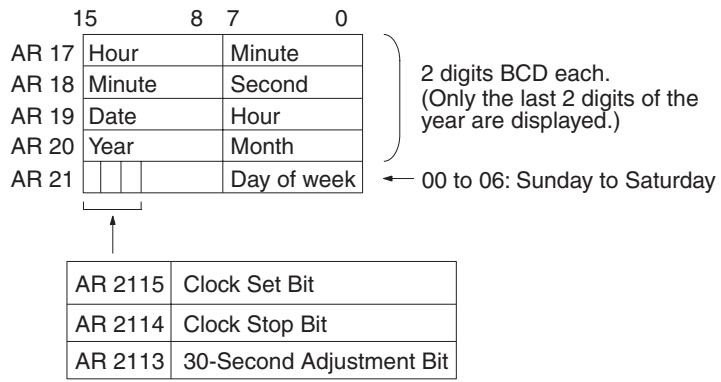
Setting the Time
To set the time, use a Programming Device as follows:
Note The time can be set easily using menu operations from a Programming Device such as a Programming Console. Refer to the CQM1H Operation Manual for the Programming Console procedure.
Setting Everything
Set the time and date with the following procedure:
1,2,3...
- Turn ON AR 2114 (Clock Stop Bit) to stop the clock and allow AR 18 through AR 21 to be overwritten.
- Using a Programming Device, set AR 18 through AR 20 (minute/second, date/hour, and year/month) and AR 2100 through AR 2107 (day of week).
- Turn ON AR 2115 (Clock Set Bit) when the time set in step 2 is reached. The clock will start operating from the time that is set, and the Clock Stop Bit and Clock Set BIt will be turned OFF automatically.
Setting Only the Seconds
It is also possible, by using AR 2113, to simply set the seconds to "00" without going through a complicated procedure. When AR 2113 is turned ON, the clock time will change as follows:
If the seconds setting is from 00 to 29, the seconds will be reset to "00" and the minute setting will remain the same.
If the seconds setting is from 30 to 59, the seconds will be reset to "00" and the minute setting will advance by one.
When the time setting is complete, AR 2113 will turn OFF automatically.
3-7 LR Area
These bits are used to share data in a 1:1 Data Link (between the CQM1H and another PC) or Controller Link Data Link. These two functions cannot use the same LR bits simultaneously.
LR bits can be used as work bits when not used for a 1:1 Data Link.
One-to-one Data Link
Two CPU Units can be connected to establish a 1:1 Data Link that shares data in the LR areas of the two PCs. A CQM1H can be linked one-to-one with any of the following PCs: CQM1H, CQM1, C200HX/HG/HE, C200HS, CPM1, CPM1A, CPM2A, CPM2C, or SRM1(-V2). Refer to 1-6-4 One-to-one Data Links for more details.
Note Because the CPM1, CPM1A, CPM2A, and SRM1(-V2) PCs have a smaller LR area, the CQM1H's link area setting (DM 6645) must be set to LR 00 to LR 15 when connecting 1:1 with one of these PCs.
Controller Link Data Link
A Controller Link Unit can be mounted to establish a Controller Link Data Link using automatic or manual settings. Refer to the Controller Link Unit's Operation Manual for more details.
3-8 Timer/Counter Area
This area is used to manage timers and counters created with TIM, TIMH(15), CNT, CNTR(12), and TTIM(—). The same numbers are used for both timers and counters and each number can be used only once in the user program. Do not use the same TIM/CNT number twice even for different instructions.
TIM/CNT numbers are used to create timers and counters, as well as to access Completion Flags and present values (PVs). If a TIM/CNT number is designated for word data, it will access the present value (PV); if it is used for bit data, it access the Completion Flag for the timer/counter.
The Completion Flag turns ON when the PV of the timer/counter that is being used goes to 0.
Refer to instructions beginning on page 233 for details on timers and counters.
Ensuring TIMH(15) Accuracy
TIM/CNT numbers 000 through 015 and interrupt processing should be used for TIMH(15) whenever the cycle time is longer than 10 ms. Using other timer/counter numbers or not using interrupt processing will lead to inaccuracy in the high-speed timers. Interrupt processing can be set in DM 6629 of the PC Setup.
Conditions Resetting TIM and TIMH(15) PVs
The PV will be reset to the SV when program execution begins, the instruction's input condition goes OFF, or the interlock condition goes OFF when the instruction is in an interlocked program section (IL–ILC).
Conditions Resetting TTIM(—) PVs
The PV will be reset to 0000 when the timer's reset input goes ON.
The PV will be maintained when program execution begins, the instruction's input condition goes OFF, or the interlock condition goes OFF when the instruction is in an interlocked program section (IL–ILC).
Conditions Resetting CNT and CNTR(12) PVs
The PV will be reset to the SV when the counter's reset input goes ON.
The PV will be maintained when program execution begins, the instruction's input condition goes OFF, or the interlock condition goes OFF when the instruction is in an interlocked program section (IL–ILC).
3-9 DM Area
Data is accessed in word units. As shown below, the read/write part of the DM area can be freely read and written from the program. The rest of the DM area is assigned specific functions in advance.
| Name | Range | |
| Read/write | All CQM1H CPU Units | DM 0000 to DM 3071 |
| CQM1H-CPU51/61 only | DM 3072 to DM 6143 | |
| Read-only area (see notes 1 and 2) | Entire read-only area | DM 6144 to DM 6568 |
| Controller Link DM parameters area | DM 6400 to DM 6409 | |
| Routing table area | DM 6450 to DM 6499 | |
| Serial Communications Board settings | DM 6550 to DM 6559 | |
| Name | Range | |
| Error log area | DM 6569 to DM 6599 | |
| PC Setup (see note 2) | DM 6600 to DM 6655 | |
Note
- The read-only area ranges from DM 6144 to DM 6568.
- The read-only area, PC Setup, program, and expansion instruction assignments can be transferred to and from the Memory Cassette as a single block of data. See 3-11 Using Memory Cassettes for details.
Read/Write DM Area
The read/write area has no particular functions assigned to it and can be used freely. It can be read and written from the program or Programming Devices. The size of the read/write area depends upon the model of CPU Unit, as shown in the following table.
| CPU Unit | Range | Access from instructions | Access from Programming Devices | ||
| Read | Write | Read | Write | ||
| CQM1H-CPU11 | DM 0000 to DM 3071 | YES | YES | YES | YES |
| CQM1H-CPU21 | |||||
| CQM1H-CPU51 | DM 0000 to DM 6143 | ||||
| CQM1H-CPU61 | |||||
Read-only Area (DM 6144 to DM 6568)
DM addresses from DM 6144 to DM 6568 make up the read-only area. Data in the read-only area can be read from instructions (not overwritten) and it can be read and overwritten from Programming Devices. Use the read-only area to store data that you don't want to be changed from the program.
To prevent data from being overwritten by Programming Devices, turn ON pin 1 on the DIP switch on the front of the CPU Unit.
When a Controller Link Unit or Serial Communications Board is being used, part of the read-only area is used for the Controller Link parameters/routing table or Serial Communications Board settings, as shown in the following table.
| Name | Range | Access from instructions | Access from Programming Devices | ||
| Read | Write | Read | Write | ||
| Controller Link DM parameters area | DM 6400 to DM 6409 | YES | No | YES | YES(See note.) |
| Routing table area | DM 6450 to DM 6499 | ||||
| Serial Communications Board settings | DM 6550 to DM 6559 | ||||
Note Data cannot be overwritten from Programming Devices when pin 1 on the DIP switch on the front of the CPU Unit is ON.
Error Log Area (DM 6569 to DM 6599)
The CPU Unit automatically records the error code and date/time of up to 10 errors (fatal and non-fatal) in the error log area.
| Access from instructions | Access from Programming Devices | ||
| Read | Write | Read | Write |
| YES | No | YES | No |
PC Setup
(DM 6600 to DM 6655)
The PC Setup contains all of the PC Setup settings except for the Serial COmmunications Board settings (stored in DM 6550 to DM 6559). Make the PC Setup settings from a Programming Device.
| Access from instructions | Access from Programming Devices | ||
| Read | Write | Read | Write |
| YES | No | YES | YES |
3-10 EM Area
The EM area can be used in CQM1H-CPU61 CPU Units only. EM data is accessed in word units. Since only one bank of EM is available, bank specification is not necessary.
EM area addresses range from EM 0000 to EM 6143. The area has no particular functions assigned to it and can be used freely. It can be read and written from the program or Programming Devices.
3-11 Using Memory Cassettes
This section provides general information on Memory Cassette specifications and explains how to read, write, and compare information in a Memory Cassette. Refer to the CQM1H Operation Manual for details on installing the Memory Cassette, write-protecting flash-memory or EEPROM Memory Cassettes, replacing EPROM chips, and changing the EPROM version switch settings.
An optional Memory Cassette can be used to record the program, read-only DM (DM 6144 to DM 6568), PC Setup (DM 6600 to DM 6655), and expansion instruction assignments. Recording this data on a Memory Cassette prevents the program and vital settings from being changed accidentally. In addition, the settings and the program required for different control processes can be easily changed by simply replacing the Memory Cassette.
The program can be written to the CPU Unit's internal RAM to operate the CQM1H without a Memory Cassette, but the CQM1H can operate even if the CPU Unit's battery fails when a Memory Cassette is used and it's contents are transferred at startup.
Clock Function
The CQM1H PCs can be equipped with a clock by installing a Memory Cassette with a clock. There is an “R” at the end of the model number of Memory Cassettes with a built-in clock. See 3-6-4 Using the Clock for more details.
Compatibility Between Different CPU Units
Data written to a Memory Cassette by a CQM1H CPU Unit cannot be read by a CQM1 CPU Unit, but data written by a CQM1 CPU Unit can be read by a CQM1H CPU Unit.
Data written to a Memory Cassette by a CQM1H-CPU61 can be read by CQM1H-CPU51, CQM1H-CPU21, and CQM1H-CPU11 CPU Units, but the program will not operate properly if EM area addresses have been used.
3-11-1 Memory Cassettes and Contents
Available Memory Cassettes
The following Memory Cassettes are available.
| Memory | Model | Specifications |
| EEPROM(see note 2) | CQM1-ME04K | 4 Kwords without clock |
| CQM1-ME04R | 4 Kwords with clock | |
| CQM1-ME08K | 8 Kwords without clock | |
| CQM1-ME08R | 8 Kwords with clock | |
| Flash (see notes 1 and 2) | CQM1H-ME16K | 16 Kwords without clock |
| CQM1H-ME16R | 16 Kwords with clock | |
| EPROM (see note 2) | CQM1-MP08K | 8 Kwords, 16 Kwords, or 32 Kwords without clock |
| CQM1-MP08R | 8 Kwords, 16 Kwords, or 32 Kwords with clock |
Note
- Data can be read and written for a EEPROM Memory Cassette with a Programming Device.
- Data can be read from a EPROM Memory Cassette with a Programming Device, but must be written with a PROM Writer. An EPROM chip with 8 Kwords, 16 Kwords, or 32 Kwords can be installed in the Memory Cassette.
- The CQM1H-ME16K and CQM1H-ME16R cannot be used in CQM1 PCs. The following EPROM chips (sold separately) are required for EPROM Memory Cassettes.
| Model | ROM version | Capacity | Access speed |
| ROM-ID-B | 27128 or equivalent | 8 Kwords | 150 ns |
| ROM-JD-B | 27256 or equivalent | 16 Kwords | 150 ns |
| ROM-KD-B | 27512 or equivalent | 32 Kwords | 150 ns |
Refer to the CQM1H Operation Manual for details on replacing EPROM chips and changing the Memory Cassette's EPROM version switch settings.
Contents
The data stored in a Memory Cassette is mainly the CPU Unit's read-only DM, PC Setup, and program, as shown in the following table. All of this data is handled as a single unit; the 4 areas cannot be read, written, or compared individually.
| Information | Contents | |
| DM area | Read-only area | Read-only DM cannot be written from the program. The range is DM 6144 to DM 6568. These words can be used freely. |
| PC Setup | The PC Setup sets the operating parameters of the CQM1H and it stored in DM 6600 to DM 6655. | |
| Expansion instruction assignments | These settings indicate which expansion instructions have been assigned function codes. | |
| User program | The entire user program | |
3-11-2 Memory Cassette Capacity and Program Size
The following table shows the largest program that can be stored in each size Memory Cassette.
| Memory Cassette size | Max. program size |
| 4 Kwords | 3.2 Kwords |
| 8 Kwords | 7.2 Kwords |
| 16 Kwords | 15.2 Kwords |
A non-fatal error will occur and the transfer will not be executed if an attempt is made to store a program that is too large for the Memory Cassette or read a program that is too large for the CPU Unit. Two examples are shown below.
1,2,3...
- When a 4-Kword EEPROM Memory Cassette is installed in a CPU Unit with a 7.2-Kword UM (user program) area, programs up to 3.2 Kwords long can be written to the Memory Cassette. A non-fatal error will occur if an at-
tempt is made to write a program larger than 3.2 Kwords to the Memory Cassette.
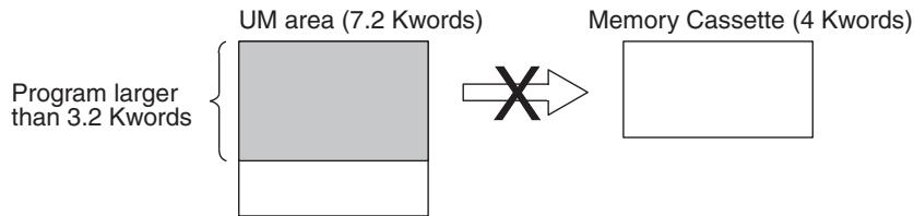
flowchart
graph LR
    A["Program larger than 3.2 Kwords"] --> B["UM area (7.2 Kwords)"]
    B --> C["Memory Cassette (4 Kwords)"]
- When a 8-Kword or larger Memory Cassette is installed in a CPU Unit with a 3.2-Kword UM (user program) area, programs up to 3.2 KW long can be read from the Memory Cassette. A non-fatal error will occur if an attempt is made to read a program larger than 3.2 Kwords from the Memory Cassette.
flowchart
graph LR
    A["UM area (3.2 Kwords)"] --> B["Memory Cassette (8 Kwords)"]
    B --> C["Program larger than 3.2 Kwords"]
Note The two transfers shown above would be completed normally if the program were 3.2 Kwords or smaller.
The approximate sizes of the programs in the UM (user program) area and Memory Cassette can be determined by the content of AR 15, as shown in the following table.
| Location | Bits | Content | Meaning |
| Memory Cassette | AR 1500 to AR 1507 | 00 | No Memory Cassette is installed or no program is saved in the Memory Cassette. |
| 04 | The program is less than 3.2 Kwords long and can be read from any CQM1H CPU Unit. | ||
| 08 | The program is less than 7.2 Kwords long and can be read from CQM1H-CPU51/61 CPU Units only. | ||
| 12 | The program is less than 11.2 Kwords long and can be read from CQM1H-CPU61 CPU Units only. | ||
| 16 | The program is less than 15.2 Kwords long and can be read from CQM1H-CPU61 CPU Units only. | ||
| UM area | AR 1508 to AR 1515 | 04 | The program is less than 3.2 Kwords long and can be written to any flash-memory or EEPROM Memory Cassette. |
| 08 | The program is less than 7.2 Kwords long and can be written to an 8-Kword or 16-Kword flash-memory or EEPROM Memory Cassette. | ||
| 12 | The program is less than 11.2 Kwords long and can be written to a 16-Kword flash-memory Memory Cassette only. | ||
| 16 | The program is less than 15.2 Kwords long and can be written to a 16-Kword flash-memory Memory Cassette only. |
In CQM1H-CPU11/21 CPU Units, the content of AR 1508 to AR 1515 is normally 04. The content of AR 1500 to AR 1507 is normally 04 when a 4-Kword Memory Cassette is installed.
The size of the program indicated in AR 15 does not include the NOP(00) instructions after END(01), but will include any instructions other than
NOP(00). Be sure to clear any unneeded instructions after END(01) to get an accurate measurement of the program's size.
3-11-3 Writing to the Memory Cassette
This section explains how to write the CPU Unit's data to a Flash-memory or EEPROM Memory Cassette.
Note A PROM Writer and Support Software are needed to write data to an EPROM Memory Cassette. Refer to the Support Software's Operation Manual for details.
Procedure
Follow the procedure outlined below to write to a Flash-memory or EEPROM Memory Cassette.
1,2,3...
- Check to see that the write-protect switch on the Memory Cassette is OFF (i.e., writing enabled). The Memory Cassette Write-protected Flag (AR 1302) will be OFF if writing is enabled.
If the switch is ON (i.e., writing not enabled), then turn the CQM1H power supply OFF and remove the Memory Cassette before changing the switch. - Check to see that the CQM1H is in PROGRAM mode. If it is in either RUN or MONITOR mode, use a Programming Device to change the mode.
- Turn ON AR 1400 from a Programming Device. The information will be written from the CQM1H to the Memory Cassette. When the operation is completed, AR 1400 will be turned OFF automatically.
Caution
Data cannot be written to the Memory Cassette if a memory error has occurred.
Note If an error occurs while data is being transmitted, a non-fatal error (FAL 9D) will be generated and the appropriate AR bit (from AR 1412 to AR 1415) will turn ON/OFF. If this occurs, refer to SECTION 8 Troubleshooting and make the necessary corrections.
3-11-4 Reading from the Memory Cassette
There are two ways to read from the Memory Cassette. The Memory Cassette to CPU Unit Transfer Bit (AR 1401) can be turned ON from a Programming Device or pin 2 of the CPU Unit's DIP switch can be turned ON to automatically read data from the Memory Cassette at startup.
If the program on the Memory Cassette has expansion instructions with function codes different from the default settings, make sure that pin 4 of the CPU Unit's DIP switch is ON (indicating user-allocated function codes).
The contents of the Memory Cassette cannot be read from the program.
Reading from the Memory Cassette can be executed regardless of the type of Memory Cassette.
If an error occurs while data is being transmitted, a non-fatal error (FAL 9D) will be generated and the appropriate AR bit (from AR 1412 to AR 1415 will turn ON/OFF. (If this occurs, refer to the Troubleshooting section and make the necessary correction.)
Programming Device Procedure
To use a Programming Device to read from the Memory Cassette, follow the procedure outlined below.
1,2,3...
-
Check to see that the CQM1H is in PROGRAM mode. If it is in either RUN or MONITOR mode, use the Programming Device to change the mode.
-
Use the Programming Device to turn ON AR 1401. The information will be read from the Memory Cassette to the CQM1H and AR 1401 will be turned OFF automatically when the read operation is completed.
Automatic Transfer at Startup
If pin 2 of the CPU Unit's DIP switch is ON, data will automatically be read from the Memory Cassette when the power supply is turned ON to the CQM1H. A memory error will occur and operation won't be possible if an error occurs during transfer of data between the Memory Cassette and CQM1H memory.

Be absolutely sure that the power is turned OFF before changing CQM1H DIP switch settings.
3-11-5 Comparing Memory Cassette Contents
The contents of the Memory Cassette can be compared to the contents of the CQM1H's memory to check to see if they are the same. This comparison can be performed for any type of Memory Cassette.
Procedure
Use the following procedure.
1,2,3...
- Check to see that the CQM1H is in PROGRAM mode. If it is in either RUN or MONITOR mode, use the Programming Device to change to PROGRAM mode.
- Turn ON AR 1402 from the Programming Device. The contents of the Memory Cassette will be compared to the contents of CQM1H memory and AR 1402 will be turned OFF automatically when the comparison is completed.
- Check the status of AR 1403 to see the results of the comparison. AR 1403 will be ON if the contents were not the same or if the comparison was not possible because the CQM1H was not in PROGRAM mode. If AR 1403 is OFF, the comparison was successful and the contents were the same.
AR 1403 cannot be controlled from the program or from a Programming Device. It is controlled by the results of comparison only.
If a comparison is attempted with the CQM1H in any mode but PROGRAM mode, a non-fatal error will occur (FAL 9D) and AR 1412 will turn ON. Although AR 1403 will also turn ON, no comparison will have been performed. AR 1403 will also turn ON if a comparison is attempted without a Memory Cassette mounted in the CQM1H.
SECTION 4
Ladder-diagram Programming
This section explains the basic steps and concepts involved in writing a basic ladder diagram program. It introduces the instructions that are used to build the basic structure of the ladder diagram and control its execution. The entire set of instructions used in programming is described in SECTION 5 Instruction Set.
4-1 Basic Procedure.... 180
4-2 Instruction Terminology 180
4-3 Basic Ladder Diagrams.... 181
4-3-1 Basic Terms 181
4-3-2 Mnemonic Code 182
4-3-3 Ladder Instructions.... 183
4-3-4 OUTPUT and OUTPUT NOT 186
4-3-5 The END Instruction.... 186
4-3-6 Logic Block Instructions.... 187
4-3-7 Coding Multiple Right-hand Instructions.... 194
4-3-8 Branching Instruction Lines 195
4-3-9 Jumps 198
4-4 Controlling Bit Status 200
4-4-1 SET and RESET.... 200
4-4-2 DIFFERENTIATE UP and DIFFERENTIATE DOWN.... 201
4-4-3 KEEP 201
4-4-4 Self-maintaining Bits (Seal) 201
4-5 Work Bits (Internal Relays) 202
4-6 Programming Precautions.... 204
4-7 Program Execution 205
4-8 Indirectly Addressing the DM and EM Areas 206
4-1 Basic Procedure
There are several basic steps involved in writing a program. Sheets that can be copied to aid in programming are provided in Appendix E I/O Assignment Sheet and Appendix F Program Coding Sheet.
1,2,3...
- Obtain a list of all I/O devices and the I/O points that have been assigned to them and prepare a table that shows the I/O bit allocated to each I/O device.
- If you are using LR bits to link two PCs, prepare sheet showing the usage of these bits.
- Determine what words are available for work bits and prepare a table in which you can allocate these as you use them.
- Also prepare tables of TC numbers and jump numbers so that you can allocate these as you use them. Remember, the function of a TC number can be defined only once within the program; jump numbers 01 through 99 can be used only once each. (TC number are described in 5-16 Timer and Counter Instructions; jump numbers are described later in this section.)
- Draw the ladder diagram.
- Input the program into the CPU Unit. When using the Programming Console, this will involve converting the program to mnemonic form.
- Check the program for syntax errors and correct these.
- Execute the program to check for execution errors and correct these.
- After the entire Control System has been installed and is ready for use, execute the program and fine tune it if required.
The basics of ladder-diagram programming and conversion to mnemonic code are described in 4-3 Basic Ladder Diagrams. Preparing for and inputting the program via the Programming Console are described in the CQM1H Operation Manual and via the CX-Programmer in the CX-Programmer User Manual.
The rest of SECTION 4 covers more advanced programming, programming precautions, and program execution. All special application instructions are covered in SECTION 5 Instruction Set. Debugging is described in the CQM1H Operation Manual and CX-Programmer User Manual. SECTION 8 Troubleshooting also provides information required for debugging.
4-2 Instruction Terminology
There are basically two types of instructions used in ladder-diagram programming: 1) instructions that correspond to the conditions on the ladder diagram and are used in instruction form only when converting a program to mnemonic code and 2) instructions that are used on the right side of the ladder diagram and are executed according to the conditions on the instruction lines leading to them.
Most instructions have at least one or more operands associated with them. Operands indicate or provide the data on which an instruction is to be performed. These are sometimes input as the actual numeric values, but are usually the addresses of data area words or bits that contain the data to be used. For instance, a MOVE instruction that has IR 000 designated as the source operand will move the contents of IR 000 to some other location. The other location is also designated as an operand. A bit whose address is designated as an operand is called an operand bit; a word whose address is designated as an operand is called an operand word. If the actual value is entered as a constant, it is preceded by # to indicate that it is not an address.
Other terms used in describing instructions are introduced in SECTION 5 Instruction Set.
4-3 Basic Ladder Diagrams
A ladder diagram consists of one line running down the left side with lines branching off to the right. The line on the left is called the bus bar. The branching lines are called instruction lines or rungs. Along the instruction lines are placed conditions that lead to other instructions on the right side. The logical combinations of these conditions determine when and how the instructions at the right are executed. A ladder diagram is shown below.
flowchart
graph TD
    A["00000 06315"] --> B["25208"]
    B --> C["HR 0109"]
    C --> D["LR 2503"]
    D --> E["24400"]
    E --> F["24401"]
    F --> G["Instruction"]
    H["00001"] --> I["00501"]
    I --> J["00502"]
    J --> K["00503"]
    K --> L["00504"]
    L --> M["Instruction"]
    N["00100 00002"] --> O["00003 HR 0050"]
    O --> P["00007 TIM 001 LR 0515"]
    P --> Q["00403"]
    Q --> R["00405"]
    R --> S["Instruction"]
    T["00010"] --> U["21001"]
    U --> V["21002"]
    V --> W["21005"]
    W --> X["21007"]
    X --> Y["21001"]
    Y --> Z["0011"]
As shown in the diagram above, instruction lines can branch apart and they can join back together. The vertical pairs of lines are called conditions. Conditions without diagonal lines through them are called normally open conditions and correspond to a LOAD, AND, or OR instruction. The conditions with diagonal lines through them are called normally closed conditions and correspond to a LOAD NOT, AND NOT, or OR NOT instruction. The number above each condition indicates the operand bit for the instruction. It is the status of the bit associated with each condition that determines the execution condition for following instructions. The way the operation of each of the instructions corresponds to a condition is described below. Before we consider these, however, there are some basic terms that must be explained.
Note When displaying ladder diagrams with the CX-Programmer, a second bus bar will be shown on the right side of the ladder diagram and will be connected to all instructions on the right side. This does not change the ladder-diagram program in any functional sense. No conditions can be placed between the instructions on the right side and the right bus bar, i.e., all instructions on the right must be connected directly to the right bus bar. Refer to the CX-Programmer User Manual for details.
4-3-1 Basic Terms
Normally Open and Normally closed Conditions
Each condition in a ladder diagram is either ON or OFF depending on the status of the operand bit that has been assigned to it. A normally open condition is ON if the operand bit is ON; OFF if the operand bit is OFF. A normally closed condition is ON if the operand bit is OFF; OFF if the operand bit is ON. Generally speaking, you use a normally open condition when you want something to happen when a bit is ON, and a normally closed condition when you want something to happen when a bit is OFF.
Instruction is executed when IR bit 00000 is ON.
Instruction is executed when IR bit 00000 is OFF.
Execution Conditions
In ladder diagram programming, the logical combination of ON and OFF conditions before an instruction determines the compound condition under which the instruction is executed. This condition, which is either ON or OFF, is called the execution condition for the instruction. All instructions other than LOAD instructions have execution conditions.
Operand Bits
The operands designated for any of the ladder instructions can be any bit in the IR, SR, HR, AR, LR, or TC areas. This means that the conditions in a ladder diagram can be determined by I/O bits, flags, work bits, timers/counters, etc. LOAD and OUTPUT instructions can also use TR area bits, but they do so only in special applications. Refer to 4-3-8 Branching Instruction Lines for details.
Logic Blocks
The way that conditions correspond to what instructions is determined by the relationship between the conditions within the instruction lines that connect them. Any group of conditions that go together to create a logic result is called a logic block. Although ladder diagrams can be written without actually analyzing individual logic blocks, understanding logic blocks is necessary for efficient programming and is essential when programs are to be input in mnemonic code.
Instruction Block
An instruction block consists of all the instructions that are interconnected across the ladder diagram. One instruction block thus consists of all the instructions between where you can draw a horizontal line across the ladder diagram without intersecting any vertical lines and the next place where you can draw the same type of horizontal line.
4-3-2 Mnemonic Code
The ladder diagram cannot be directly input into the PC via a Programming Console; the CX-Programmer is required. To input from a Programming Console, it is necessary to convert the ladder diagram to mnemonic code. The mnemonic code provides exactly the same information as the ladder diagram, but in a form that can be typed directly into the PC. Actually you can program directly in mnemonic code, although it is not recommended for beginners or for complex programs. Also, regardless of the Programming Device used, the program is stored in memory in mnemonic form, making it important to understand mnemonic code.
Because of the importance of the Programming Console as a peripheral device and because of the importance of mnemonic code in complete understanding of a program, we will introduce and describe the mnemonic code along with the ladder diagram. Remember, you will not need to use the mnemonic code if you are inputting via the CX-Programmer (although you can use it with the CX-Programmer if you prefer).
Program Memory Structure
The program is input into addresses in Program Memory. Addresses in Program Memory are slightly different to those in other memory areas because each address does not necessarily hold the same amount of data. Rather, each address holds one instruction and all of the definers and operands (described in more detail later) required for that instruction. Because some
instructions require no operands, while others require up to three operands, Program Memory addresses can be from one to four words long.
Program Memory addresses start at 00000 and run until the capacity of Program Memory has been exhausted. The first word at each address defines the instruction. Any definers used by the instruction are also contained in the first word. Also, if an instruction requires only a single bit operand (with no definer), the bit operand is also programmed on the same line as the instruction. The rest of the words required by an instruction contain the operands that specify what data is to be used. When converting to mnemonic code, all but ladder diagram instructions are written in the same form, one word to a line, just as they appear in the ladder diagram symbols. An example of mnemonic code is shown below. The instructions used in it are described later in the manual.
| Address | Instruction | Operands | |
| 00000 | LD | HR | 0001 |
| 00001 | AND | 00001 | |
| 00002 | OR | 00002 | |
| 00003 | LD NOT | 00100 | |
| 00004 | AND | 00101 | |
| 00005 | AND LD | ||
| 00006 | MOV(21) | ||
| 000 | |||
| DM | 0000 | ||
| 00007 | CMP(20) | ||
| DM | 0000 | ||
| HR | 00 | ||
| 00008 | AND | 25505 | |
| 00009 | OUT | 10000 | |
| 00010 | MOV(21) | ||
| DM | 0000 | ||
| DM | 0500 | ||
| 00011 | LD | 00502 | |
| 00012 | AND | 00005 | |
| 00013 | OUT | 10003 | |
The address and instruction columns of the mnemonic code table are filled in for the instruction word only. For all other lines, the left two columns are left blank. If the instruction requires no definer or bit operand, the operand column is left blank for first line. It is a good idea to cross through any blank data column spaces (for all instruction words that do not require data) so that the data column can be quickly scanned to see if any addresses have been left out.
When programming, addresses are automatically displayed and do not have to be input unless for some reason a different location is desired for the instruction. When converting to mnemonic code, it is best to start at Program Memory address 00000 unless there is a specific reason for starting elsewhere.
4-3-3 Ladder Instructions
The ladder instructions are those instructions that correspond to the conditions on the ladder diagram. Ladder instructions, either independently or in combination with the logic block instructions described next, form the execution conditions upon which the execution of all other instructions are based.
LOAD and LOAD NOT
The first condition that starts any logic block within a ladder diagram corresponds to a LOAD or LOAD NOT instruction. Each of these instruction requires one line of mnemonic code. "Instruction" is used as a dummy instruction in the following examples and could be any of the right-hand instructions described later in this manual.
| Address | Instruction | Operands |
| 00000 | LD | 00000 |
| 00001 | Instruction | |
| 00002 | LD NOT | 00000 |
| 00003 | Instruction |
When this is the only condition on the instruction line, the execution condition for the instruction at the right is ON when the condition is ON. For the LOAD instruction (i.e., a normally open condition), the execution condition would be ON when IR 00000 was ON; for the LOAD NOT instruction (i.e., a normally closed condition), it would be ON when 00000 was OFF.
AND and AND NOT
When two or more conditions lie in series on the same instruction line, the first one corresponds to a LOAD or LOAD NOT instruction; and the rest of the conditions, to AND or AND NOT instructions. The following example shows three conditions which correspond in order from the left to a LOAD, an AND NOT, and an AND instruction. Again, each of these instructions requires one line of mnemonic code.
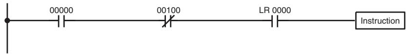
| Address | Instruction | Operands |
| 00000 | LD | 00000 |
| 00001 | AND NOT | 00100 |
| 00002 | AND | LR 0000 |
| 00003 | Instruction |
The instruction would have an ON execution condition only when all three conditions are ON, i.e., when IR 00000 was ON, IR 00100 was OFF, and LR 0000 was ON.
AND instructions in series can be considered individually, with each taking the logical AND of the execution condition (i.e., the total of all conditions up to that point) and the status of the AND instruction's operand bit. If both of these are ON, an ON execution condition will be produced for the next instruction. If either is OFF, the result will also be OFF. The execution condition for the first AND instruction in a series is the first condition on the instruction line.
Each AND NOT instruction in a series would take the logical AND between its execution condition and the inverse of its operand bit.
OR and OR NOT
When two or more conditions lie on separate instruction lines running in parallel and then joining together, the first condition corresponds to a LOAD or LOAD NOT instruction; the rest of the conditions correspond to OR or OR NOT instructions. The following example shows three conditions which correspond in order from the top to a LOAD NOT, an OR NOT, and an OR instruction. Again, each of these instructions requires one line of mnemonic code.
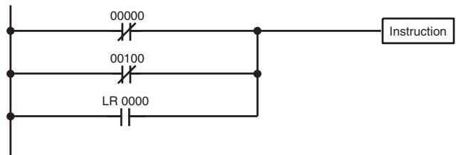
| Address | Instruction | Operands |
| 00000 | LD NOT | 00000 |
| 00001 | OR NOT | 00100 |
| 00002 | OR | LR 0000 |
| 00003 | Instruction |
The instruction would have an ON execution condition when any one of the three conditions was ON, i.e., when IR 00000 was OFF, when IR 00100 was OFF, or when LR 0000 was ON.
OR and OR NOT instructions can be considered individually, each taking the logical OR between its execution condition and the status of the OR instruction's operand bit. If either one of these were ON, an ON execution condition would be produced for the next instruction.
Combining AND and OR Instructions
When AND and OR instructions are combined in more complicated diagrams, they can sometimes be considered individually, with each instruction performing a logic operation on the execution condition and the status of the operand bit. The following is one example. Study this example until you are convinced that the mnemonic code follows the same logic flow as the ladder diagram.
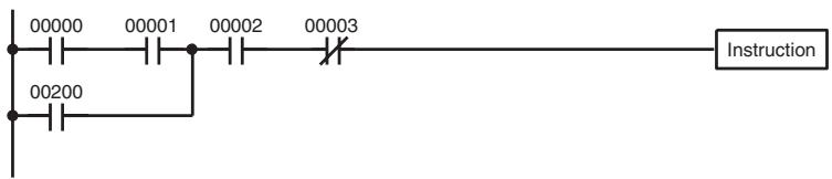
| Address | Instruction | Operands |
| 00000 | LD | 00000 |
| 00001 | AND | 00001 |
| 00002 | OR | 00200 |
| 00003 | AND | 00002 |
| 00004 | AND NOT | 00003 |
| 00005 | Instruction |
Here, an AND is taken between the status of IR 00000 and that of IR 00001 to determine the execution condition for an OR with the status of IR 00200. The result of this operation determines the execution condition for an AND with the status of IR 00002, which in turn determines the execution condition for an AND with the inverse (i.e., and AND NOT) of the status of IR 00003.
In more complicated diagrams, however, it is necessary to consider logic blocks before an execution condition can be determined for the final instruction, and that's where AND LOAD and OR LOAD instructions are used. Before we consider more complicated diagrams, however, we'll look at the instructions required to complete a simple "input-output" program.
4-3-4 OUTPUT and OUTPUT NOT
The simplest way to output the results of combining execution conditions is to output it directly with the OUTPUT and OUTPUT NOT. These instructions are used to control the status of the designated operand bit according to the execution condition. With the OUTPUT instruction, the operand bit will be turned ON as long as the execution condition is ON and will be turned OFF as long as the execution condition is OFF. With the OUTPUT NOT instruction, the operand bit will be turned ON as long as the execution condition is OFF and turned OFF as long as the execution condition is ON. These appear as shown below. In mnemonic code, each of these instructions requires one line.
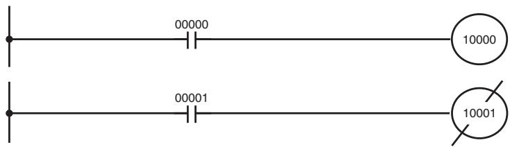
| Address | Instruction | Operands |
| 00000 | LD | 00000 |
| 00001 | OUT | 10000 |
| Address | Instruction | Operands |
| 00000 | LD | 00001 |
| 00001 | OUT NOT | 10001 |
In the above examples, IR 10000 will be ON as long as IR 00000 is ON and IR 10001 will be OFF as long as IR 00001 is ON. Here, IR 00000 and IR 00001 would be input bits and IR 10000 and IR 10001 output bits assigned to the Units controlled by the PC, i.e., the signals coming in through the input points assigned IR 00000 and IR 00001 are controlling the output points assigned IR 10000 and IR 10001, respectively.
The length of time that a bit is ON or OFF can be controlled by combining the OUTPUT or OUTPUT NOT instruction with Timer instructions. Refer to Examples under 5-16-1 TIMER - TIM for details.
4-3-5 The END Instruction
The last instruction required to complete a simple program is the END instruction. When the CPU Unit scans the program, it executes all instructions up to the first END instruction before returning to the beginning of the program and beginning execution again. Although an END instruction can be placed at any point in a program, which is sometimes done when debugging, no instructions past the first END instruction will be executed until it is removed. The number following the END instruction in the mnemonic code is its function code, which is used when inputting most instruction into the PC. These are described later. The END instruction requires no operands and no conditions can be placed on the same instruction line with it.
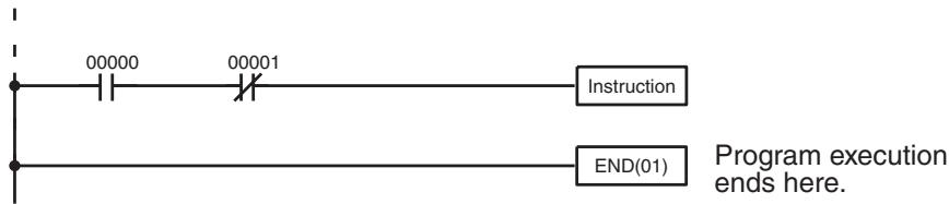
flowchart
graph LR
    A["00000"] --> B["00001"]
    B --> C["Instruction"]
    D["END(01)"] --> E["Program execution ends here"]
| Address | Instruction | Operands |
| 00500 | LD | 00000 |
| 00501 | AND NOT | 00001 |
| 00502 | Instruction | |
| 00503 | END(01) | --- |
If there is no END instruction anywhere in the program, the program will not be executed at all.
Now you have all of the instructions required to write simple input-output programs. Before we finish with ladder diagram basic and go onto inputting the program into the PC, let's look at logic block instruction (AND LOAD and OR LOAD), which are sometimes necessary even with simple diagrams.
4-3-6 Logic Block Instructions
Logic block instructions do not correspond to specific conditions on the ladder diagram; rather, they describe relationships between logic blocks. The AND LOAD instruction logically ANDs the execution conditions produced by two logic blocks. The OR LOAD instruction logically ORs the execution conditions produced by two logic blocks.
AND LOAD
Although simple in appearance, the diagram below requires an AND LOAD instruction.
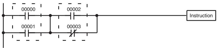
| Address | Instruction | Operands |
| 00000 | LD | 00000 |
| 00001 | OR | 00001 |
| 00002 | LD | 00002 |
| 00003 | OR NOT | 00003 |
| 00004 | AND LD | --- |
The two logic blocks are indicated by dotted lines. Studying this example shows that an ON execution condition will be produced when: either of the conditions in the left logic block is ON (i.e., when either IR 00000 or IR 00001 is ON), and when either of the conditions in the right logic block is ON (i.e., when either IR 00002 is ON or IR 00003 is OFF).
The above ladder diagram cannot, however, be converted to mnemonic code using AND and OR instructions alone. If an AND between IR 00002 and the results of an OR between IR 00000 and IR 00001 is attempted, the OR NOT between IR 00002 and IR 00003 is lost and the OR NOT ends up being an OR NOT between just IR 00003 and the result of an AND between IR 00002 and the first OR. What we need is a way to do the OR (NOT)'s independently and then combine the results.
To do this, we can use the LOAD or LOAD NOT instruction in the middle of an instruction line. When LOAD or LOAD NOT is executed in this way, the current execution condition is saved in special buffers and the logic process is repeated from the beginning. To combine the results of the current execution condition with that of a previous “unused” execution condition, an AND LOAD or an OR LOAD instruction is used. Here “LOAD” refers to loading the last unused execution condition. An unused execution condition is produced by using the LOAD or LOAD NOT instruction for any but the first condition on an instruction line.
Analyzing the above ladder diagram in terms of mnemonic instructions, the condition for IR 00000 is a LOAD instruction and the condition below it is an OR instruction between the status of IR 00000 and that of IR 00001. The condition at IR 00002 is another LOAD instruction and the condition below is an OR NOT instruction, i.e., an OR between the status of IR 00002 and the inverse of the status of IR 00003. To arrive at the execution condition for the instruction at the right, the logical AND of the execution conditions resulting
from these two blocks would have to be taken. AND LOAD does this. The mnemonic code for the ladder diagram is shown below. The AND LOAD instruction requires no operands of its own, because it operates on previously determined execution conditions. Here too, dashes are used to indicate that no operands needs designated or input.
OR LOAD
The following diagram requires an OR LOAD instruction between the top logic block and the bottom logic block. An ON execution condition would be produced for the instruction at the right either when IR 00000 is ON and IR 00001 is OFF or when IR 00002 and IR 00003 are both ON. The operation of and mnemonic code for the OR LOAD instruction are exactly the same as those for a AND LOAD instruction except that the current execution condition is ORed with the last unused execution condition.

| Address | Instruction | Operands |
| 00000 | LD | 00000 |
| 00001 | AND NOT | 00001 |
| 00002 | LD | 00002 |
| 00003 | AND | 00003 |
| 00004 | OR LD | --- |
Naturally, some diagrams will require both AND LOAD and OR LOAD instructions.
Logic Block Instructions in Series
To code diagrams with logic block instructions in series, the diagram must be divided into logic blocks. Each block is coded using a LOAD instruction to code the first condition, and then AND LOAD or OR LOAD is used to logically combine the blocks. With both AND LOAD and OR LOAD there are two ways to achieve this. One is to code the logic block instruction after the first two blocks and then after each additional block. The other is to code all of the blocks to be combined, starting each block with LOAD or LOAD NOT, and then to code the logic block instructions which combine them. In this case, the instructions for the last pair of blocks should be combined first, and then each preceding block should be combined, working progressively back to the first block. Although either of these methods will produce exactly the same result, the second method, that of coding all logic block instructions together, can be used only if eight or fewer blocks are being combined, i.e., if seven or fewer logic block instructions are required.
The following diagram requires AND LOAD to be converted to mnemonic code because three pairs of parallel conditions lie in series. The two means of coding the programs are also shown.

| Address | Instruction | Operands |
| 00000 | LD | 00000 |
| 00001 | OR NOT | 00001 |
| 00002 | LD NOT | 00002 |
| 00003 | OR | 00003 |
| 00004 | AND LD | — |
| 00005 | LD | 00004 |
| 00006 | OR | 00005 |
| 00007 | AND LD | — |
| 00008 | OUT | 10000 |
| Address | Instruction | Operands |
| 00000 | LD | 00000 |
| 00001 | OR NOT | 00001 |
| 00002 | LD NOT | 00002 |
| 00003 | OR | 00003 |
| 00004 | LD | 00004 |
| 00005 | OR | 00005 |
| 00006 | AND LD | — |
| 00007 | AND LD | — |
| 00008 | OUT | 10000 |
Again, with the method on the right, a maximum of eight blocks can be combined. There is no limit to the number of blocks that can be combined with the first method.
The following diagram requires OR LOAD instructions to be converted to mnemonic code because three pairs of conditions in series lie in parallel to each other.
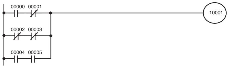
flowchart
graph TD
    A["00000 00001"] --> B["10001"]
    C["00002 00003"] --> B
    D["00004 00005"] --> B
    B --> E["Output"]
The first of each pair of conditions is converted to LOAD with the assigned bit operand and then ANDed with the other condition. The first two blocks can be coded first, followed by OR LOAD, the last block, and another OR LOAD, or the three blocks can be coded first followed by two OR LOADs. The mnemonic code for both methods is shown below.
| Address | Instruction | Operands |
| 00000 | LD | 00000 |
| 00001 | AND NOT | 00001 |
| 00002 | LD NOT | 00002 |
| 00003 | AND NOT | 00003 |
| 00004 | OR LD | — |
| 00005 | LD | 00004 |
| 00006 | AND | 00005 |
| 00007 | OR LD | — |
| 00008 | OUT | 10001 |
| Address | Instruction | Operands |
| 00000 | LD | 00000 |
| 00001 | AND NOT | 00001 |
| 00002 | LD NOT | 00002 |
| 00003 | AND NOT | 00003 |
| 00004 | LD | 00004 |
| 00005 | AND | 00005 |
| 00006 | OR LD | — |
| 00007 | OR LD | — |
| 00008 | OUT | 10001 |
Again, with the method on the right, a maximum of eight blocks can be combined. There is no limit to the number of blocks that can be combined with the first method.
Combining AND LOAD and OR LOAD
Both of the coding methods described above can also be used when using AND LOAD and OR LOAD, as long as the number of blocks being combined does not exceed eight.
The following diagram contains only two logic blocks as shown. It is not necessary to further separate block b components, because it can be coded directly using only AND and OR.
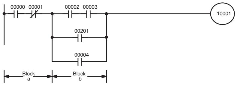
| Address | Instruction | Operands |
| 00000 | LD | 00000 |
| 00001 | AND NOT | 00001 |
| 00002 | LD | 00002 |
| 00003 | AND | 00003 |
| 00004 | OR | 00201 |
| 00005 | OR | 00004 |
| 00006 | AND LD | — |
| 00007 | OUT | 10001 |
Although the following diagram is similar to the one above, block b in the diagram below cannot be coded without separating it into two blocks combined with OR LOAD. In this example, the three blocks have been coded first and then OR LOAD has been used to combine the last two blocks followed by AND LOAD to combine the execution condition produced by the OR LOAD with the execution condition of block a.
When coding the logic block instructions together at the end of the logic blocks they are combining, they must, as shown below, be coded in reverse order, i.e., the logic block instruction for the last two blocks is coded first, followed by the one to combine the execution condition resulting from the first logic block instruction and the execution condition of the logic block third from the end, and on back to the first logic block that is being combined.
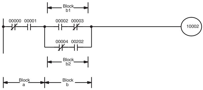
| Address | Instruction | Operands |
| 00000 | LD NOT | 00000 |
| 00001 | AND | 00001 |
| 00002 | LD | 00002 |
| 00003 | AND NOT | 00003 |
| 00004 | LD NOT | 00004 |
| 00005 | AND | 00202 |
| 00006 | OR LD | — |
| 00007 | AND LD | — |
| 00008 | OUT | 10002 |
Complicated Diagrams
When determining what logic block instructions will be required to code a diagram, it is sometimes necessary to break the diagram into large blocks and then continue breaking the large blocks down until logic blocks that can be coded without logic block instructions have been formed. These blocks are then coded, combining the small blocks first, and then combining the larger blocks. Either AND LOAD or OR LOAD is used to combine the blocks, i.e., AND LOAD or OR LOAD always combines the last two execution conditions that existed, regardless of whether the execution conditions resulted from a single condition, from logic blocks, or from previous logic block instructions.
When working with complicated diagrams, blocks will ultimately be coded starting at the top left and moving down before moving across. This will generally mean that, when there might be a choice, OR LOAD will be coded before AND LOAD.
The following diagram must be broken down into two blocks and each of these then broken into two blocks before it can be coded. As shown below, blocks a and b require an AND LOAD. Before AND LOAD can be used, however, OR LOAD must be used to combine the top and bottom blocks on both sides, i.e., to combine a1 and a2; b1 and b2.
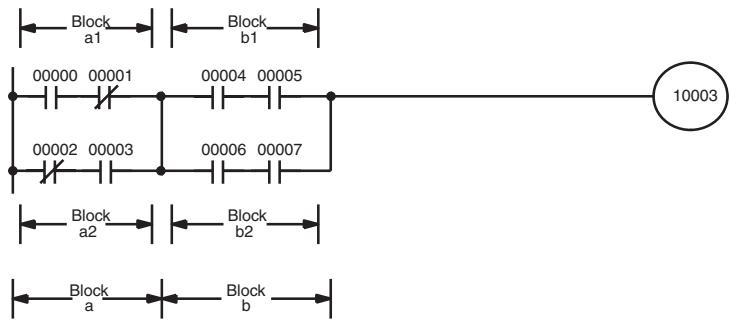
flowchart
graph TD
    A["Block a1"] --> B["Block b1"]
    C["00000 00001"] --> D["00004 00005"]
    E["00002 00003"] --> F["00006 00007"]
    G["Block a2"] --> H["Block b2"]
    I["Block a"] --> J["Block b"]
| Address | Instruction | Operands |
| 00000 | LD | 00000 |
| 00001 | AND NOT | 00001 |
| 00002 | LD NOT | 00002 |
| 00003 | AND | 00003 |
| 00004 | OR LD | — |
| 00005 | LD | 00004 |
| 00006 | AND | 00005 |
| 00007 | LD | 00006 |
| 00008 | AND | 00007 |
| 00009 | OR LD | — |
| 00010 | AND LD | — |
| 00011 | OUT | 10003 |
Blocks a1 and a2
Blocks b1 and b2
Blocks a and b
The following type of diagram can be coded easily if each block is coded in order: first top to bottom and then left to right. In the following diagram, blocks a and b would be combined using AND LOAD as shown above, and then block c would be coded and a second AND LOAD would be used to combine it with the execution condition from the first AND LOAD. Then block d would be coded, a third AND LOAD would be used to combine the execution condition from block d with the execution condition from the second AND LOAD, and so on through to block n.
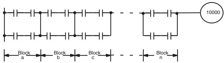
The following diagram requires an OR LOAD followed by an AND LOAD to code the top of the three blocks, and then two more OR LOADs to complete the mnemonic code.
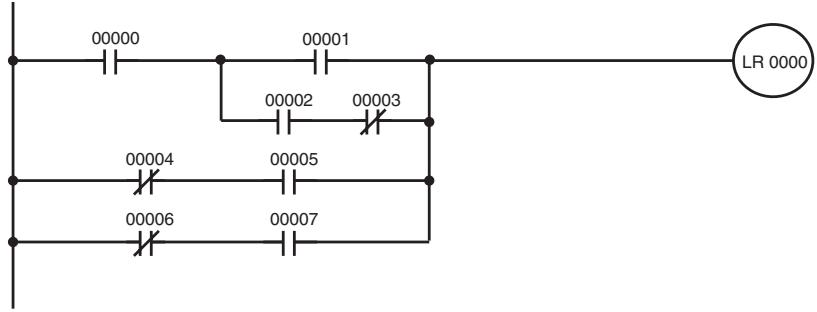
| Address | Instruction | Operands |
| 00000 | LD | 00000 |
| 00001 | LD | 00001 |
| 00002 | LD | 00002 |
| 00003 | AND NOT | 00003 |
| 00004 | OR LD | -- |
| 00005 | AND LD | -- |
| 00006 | LD NOT | 00004 |
| 00007 | AND | 00005 |
| 00008 | OR LD | -- |
| 00009 | LD NOT | 00006 |
| 00010 | AND | 00007 |
| 00011 | OR LD | -- |
| 00012 | OUT | LR 0000 |
Although the program will execute as written, this diagram could be drawn as shown below to eliminate the need for the first OR LOAD and the AND LOAD, simplifying the program and saving memory space.
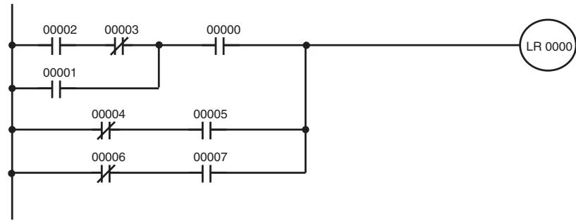
| Address | Instruction | Operands |
| 00000 | LD | 00002 |
| 00001 | AND NOT | 00003 |
| 00002 | OR | 00001 |
| 00003 | AND | 00000 |
| 00004 | LD NOT | 00004 |
| 00005 | AND | 00005 |
| 00006 | OR LD | -- |
| 00007 | LD NOT | 00006 |
| 00008 | AND | 00007 |
| 00009 | OR LD | -- |
| 00010 | OUT | LR 0000 |
The following diagram requires five blocks, which here are coded in order before using OR LOAD and AND LOAD to combine them starting from the last two blocks and working backward. The OR LOAD at program address 00008 combines blocks d and e, the following AND LOAD combines the resulting execution condition with that of block c, etc.
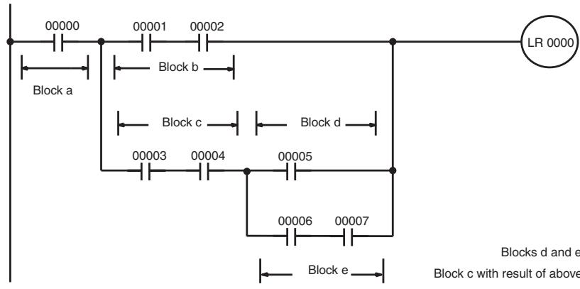
flowchart
graph TD
    A["00000"] --> B["Block a"]
    C["00001"] --> D["Block b"]
    E["00002"] --> F["Block c"]
    G["LR 0000"] --> H["Block d"]
    I["00003"] --> J["Block e"]
    K["00004"] --> L["Block e"]
    M["00005"] --> N["Block e"]
    O["00006"] --> P["Block e"]
    Q["00007"] --> R["Block e"]
    S["Blocks d and e"] --> T["Block c with result of above"]
| Address | Instruction | Operands |
| 00000 | LD | 00000 |
| 00001 | LD | 00001 |
| 00002 | AND | 00002 |
| 00003 | LD | 00003 |
| 00004 | AND | 00004 |
| 00005 | LD | 00005 |
| 00006 | LD | 00006 |
| 00007 | AND | 00007 |
| 00008 | OR LD | -- |
| 00009 | AND LD | -- |
| 00010 | OR LD | -- |
| 00011 | AND LD | -- |
| 00012 | OUT | LR 0000 |
Again, this diagram can be redrawn as follows to simplify program structure and coding and to save memory space.
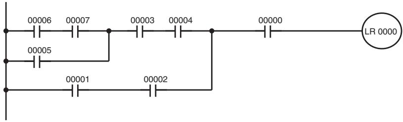
| Address | Instruction | Operands |
| 00000 | LD | 00006 |
| 00001 | AND | 00007 |
| 00002 | OR | 00005 |
| 00003 | AND | 00003 |
| 00004 | AND | 00004 |
| 00005 | LD | 00001 |
| 00006 | AND | 00002 |
| 00007 | OR LD | -- |
| 00008 | AND | 00000 |
| 00009 | OUT | LR 0000 |
The next and final example may at first appear very complicated but can be coded using only two logic block instructions. The diagram appears as follows:
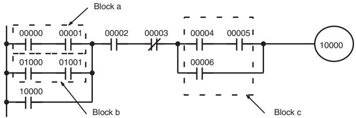
flowchart
graph TD
    A["00000"] --> B["Block a"]
    C["00001"] --> D["00002"]
    E["01000"] --> F["01001"]
    G["10000"] --> H["Block b"]
    I["00003"] --> J["00004"]
    K["00005"] --> L["10000"]
    M["00006"] --> N["Block c"]
    O["Block c"] --> P["Output"]
The first logic block instruction is used to combine the execution conditions resulting from blocks a and b, and the second one is to combine the execution condition of block c with the execution condition resulting from the normally closed condition assigned IR 00003. The rest of the diagram can be coded with OR, AND, and AND NOT instructions. The logical flow for this and the resulting code are shown below.
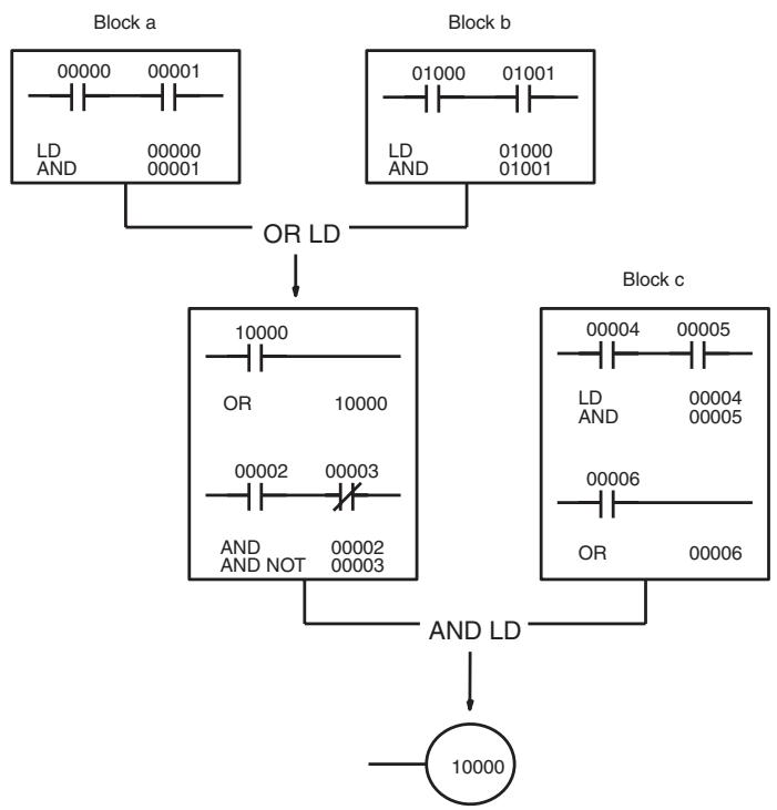
flowchart
graph TD
    A["Block a\n00000 00001\nLD AND 00000 00001"] --> D["OR LD"]
    B["Block b\n01000 01001\nLD AND 01000 01001"] --> D
    D --> E["Block c\n00004 00005\nLD AND 00004 00005"]
    E --> F["AND LD"]
    F --> G["10000"]
| Address | Instruction | Operands |
| 00000 | LD | 00000 |
| 00001 | AND | 00001 |
| 00002 | LD | 01000 |
| 00003 | AND | 01001 |
| 00004 | OR LD | -- |
| 00005 | OR | 10000 |
| 00006 | AND | 00002 |
| 00007 | AND NOT | 00003 |
| 00008 | LD | 00004 |
| 00009 | AND | 00005 |
| 00010 | OR | 00006 |
| 00011 | AND LD | -- |
| 00012 | OUT | 10000 |
4-3-7 Coding Multiple Right-hand Instructions
If there is more than one right-hand instruction executed with the same execution condition, they are coded consecutively following the last condition on the instruction line. In the following example, the last instruction line contains one more condition that corresponds to an AND with IR 00004.
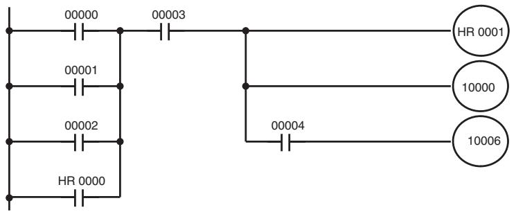
flowchart
graph TD
    A["00000"] --> B["00003"]
    C["00001"] --> B
    D["00002"] --> B
    E["HR 0000"] --> B
    B --> F["HR 0001"]
    B --> G["10000"]
    B --> H["10006"]
    I["00004"] --> H
| Address | Instruction | Operands |
| 00000 | LD | 00000 |
| 00001 | OR | 00001 |
| 00002 | OR | 00002 |
| 00003 | OR | HR 0000 |
| 00004 | AND | 00003 |
| 00005 | OUT | HR 0001 |
| 00006 | OUT | 10000 |
| 00007 | AND | 00004 |
| 00008 | OUT | 10006 |
4-3-8 Branching Instruction Lines
When an instruction line branches into two or more lines, it is sometimes necessary to use either interlocks or TR bits to maintain the execution condition that existed at a branching point. This is because instruction lines are executed across to a right-hand instruction before returning to the branching point to execute instructions on a branch line. If a condition exists on any of the instruction lines after the branching point, the execution condition could change during this time making proper execution impossible. The following diagrams illustrate this. In both diagrams, instruction 1 is executed before returning to the branching point and moving on to the branch line leading to instruction 2.
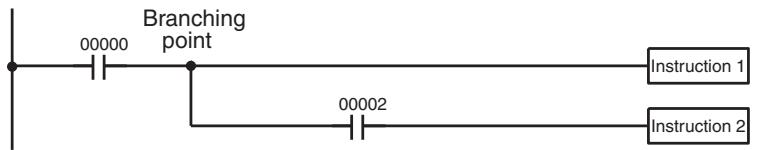
Diagram A: Correct Operation
| Address | Instruction | Operands |
| 00000 | LD | 00000 |
| 00001 | Instruction 1 | |
| 00002 | AND | 00002 |
| 00003 | Instruction 2 |
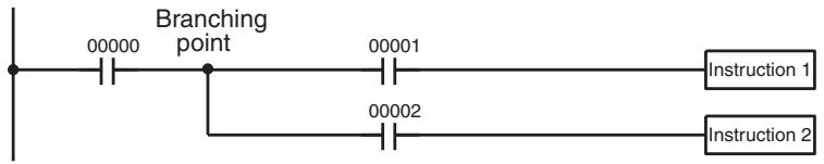
flowchart
graph LR
    A["00000"] --> B["Branching point"]
    B --> C["00001"]
    B --> D["00002"]
    E["Instruction 1"] --> F
    G["Instruction 2"] --> H
Diagram B: Incorrect Operation
| Address | Instruction | Operands |
| 00000 | LD | 00000 |
| 00001 | AND | 00001 |
| 00002 | Instruction 1 | |
| 00003 | AND | 00002 |
| 00004 | Instruction 2 |
If, as shown in diagram A, the execution condition that existed at the branching point cannot be changed before returning to the branch line (instructions at the far right do not change the execution condition), then the branch line will be executed correctly and no special programming measure is required.
If, as shown in diagram B, a condition exists between the branching point and the last instruction on the top instruction line, the execution condition at the branching point and the execution condition after completing the top instruction line will sometimes be different, making it impossible to ensure correct execution of the branch line.
There are two means of programming branching programs to preserve the execution condition. One is to use TR bits; the other, to use interlocks (IL(02)/IL(03)).
TR Bits
The TR area provides eight bits, TR 0 through TR 7, that can be used to temporarily preserve execution conditions. If a TR bit is placed at a branching point, the current execution condition will be stored at the designated TR bit. When returning to the branching point, the TR bit restores the execution status that was saved when the branching point was first reached in program execution.
The previous diagram B can be written as shown below to ensure correct execution. In mnemonic code, the execution condition is stored at the branching point using the TR bit as the operand of the OUTPUT instruction. This execution condition is then restored after executing the right-hand instruction by using the same TR bit as the operand of a LOAD instruction
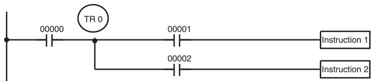
Diagram B: Corrected Using a TR bit
| Address | Instruction | Operands |
| 00000 | LD | 00000 |
| 00001 | OUT | TR 0 |
| 00002 | AND | 00001 |
| 00003 | Instruction 1 | |
| 00004 | LD | TR 0 |
| 00005 | AND | 00002 |
| 00006 | Instruction 2 |
In terms of actual instructions the above diagram would be as follows: The status of IR 00000 is loaded (a LOAD instruction) to establish the initial execution condition. This execution condition is then output using an OUTPUT instruction to TR 0 to store the execution condition at the branching point. The execution condition is then ANDed with the status of IR 00001 and instruction 1 is executed accordingly. The execution condition that was stored at the branching point is then re-loaded (a LOAD instruction with TR 0 as the operand), this is ANDed with the status of IR 00002, and instruction 2 is executed accordingly.
The following example shows an application using two TR bits.
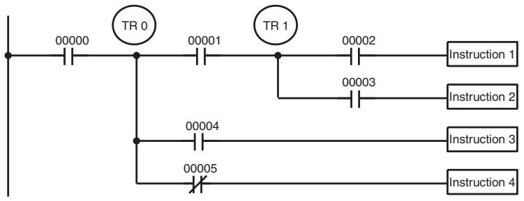
flowchart
graph TD
    A["00000"] --> B["TR 0"]
    B --> C["00001"]
    B --> D["TR 1"]
    D --> E["00002"]
    D --> F["00003"]
    F --> G["Instruction 1"]
    F --> H["Instruction 2"]
    F --> I["Instruction 3"]
    F --> J["Instruction 4"]
    B --> K["00004"]
    K --> L["00005"]
| Address | Instruction | Operands |
| 00000 | LD | 00000 |
| 00001 | OUT | TR 0 |
| 00002 | AND | 00001 |
| 00003 | OUT | TR 1 |
| 00004 | AND | 00002 |
| 00005 | Instruction 1 | |
| 00006 | LD | TR 1 |
| 00007 | AND | 00003 |
| 00008 | Instruction 2 | |
| 00009 | LD | TR 0 |
| 00010 | AND | 00004 |
| 00011 | Instruction 3 | |
| 00012 | LD | TR 0 |
| 00013 | AND NOT | 00005 |
| 00014 | Instruction 4 |
In this example, TR 0 and TR 1 are used to store the execution conditions at the branching points. After executing instruction 1, the execution condition stored in TR 1 is loaded for an AND with the status IR 00003. The execution condition stored in TR 0 is loaded twice, the first time for an AND with the status of IR 00004 and the second time for an AND with the inverse of the status of IR 00005.
TR bits can be used as many times as required as long as the same TR bit is not used more than once in the same instruction block. Here, a new instruction block is begun each time execution returns to the bus bar. If, in a single instruction block, it is necessary to have more than eight branching points that require the execution condition to be saved, interlocks (which are described next) must be used.
When drawing a ladder diagram, be careful not to use TR bits unless necessary. Often the number of instructions required for a program can be reduced and ease of understanding a program increased by redrawing a diagram that would otherwise require TR bits. In both of the following pairs of diagrams, the bottom versions require fewer instructions and do not require TR bits. In the first example, this is achieved by reorganizing the parts of the instruction
block: the bottom one, by separating the second OUTPUT instruction and using another LOAD instruction to create the proper execution condition for it.
Note Although simplifying programs is always a concern, the order of execution of instructions is sometimes important. For example, a MOVE instruction may be required before the execution of a BINARY ADD instruction to place the proper data in the required operand word. Be sure that you have considered execution order before reorganizing a program to simplify it.
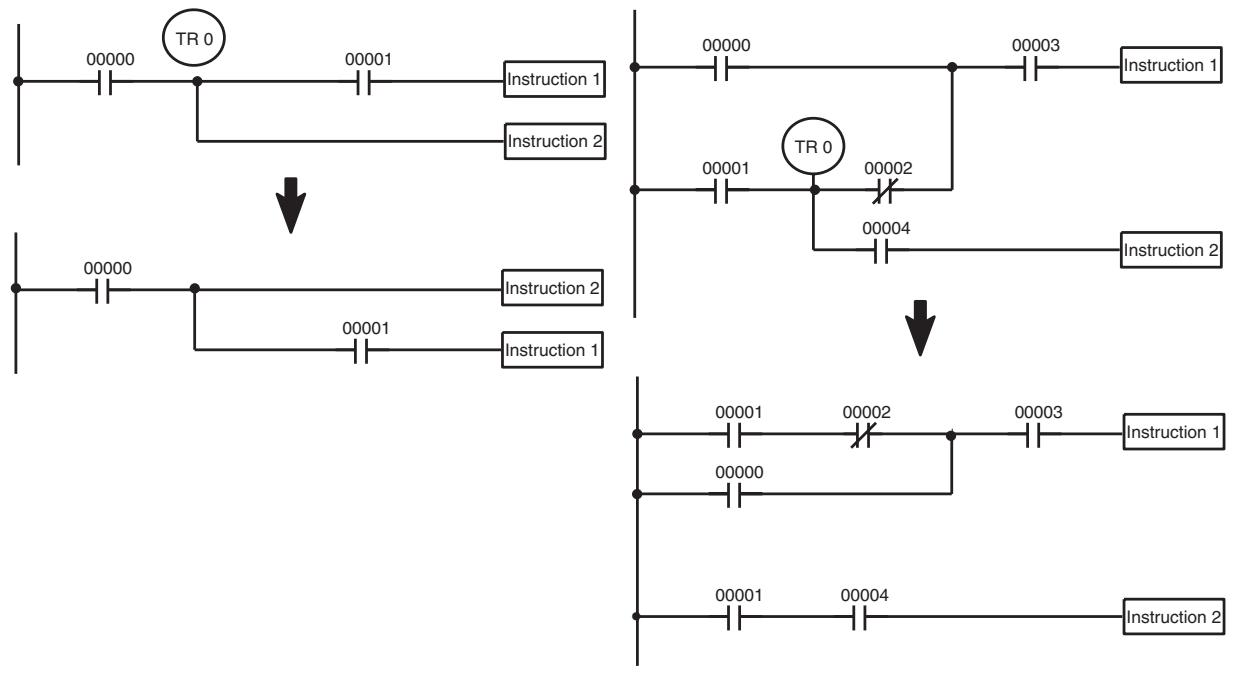
flowchart
graph TD
    subgraph Top_Lower_Circuit
        A["00000"] --> B["TR 0"]
        C["00001"] --> D["Instruction 1"]
        E["00001"] --> F["Instruction 2"]
    end

    subgraph Middle_Lower_Circuit
        G["00000"] --> H["TR 0"]
        I["00001"] --> J["Instruction 2"]
        K["00001"] --> L["Instruction 1"]
        M["00002"] --> N["TR 0"]
        O["00004"] --> P["Instruction 2"]
    end

    subgraph Bottom_Lower_Circuit
        Q["00001"] --> R["Instruction 1"]
        S["00002"] --> T["Instruction 2"]
        U["00003"] --> V["Instruction 2"]
    end
Note TR bits are must be input by the user only when programming using mnemonic code. They are not necessary when inputting ladder diagrams directly because they are processed for you automatically. The above limitations on the number of branching points requiring TR bits, and considerations on methods to reduce the number of programming instructions, still hold.
Interlocks
The problem of storing execution conditions at branching points can also be handled by using the INTERLOCK (IL(02)) and INTERLOCK CLEAR (ILC(03)) instructions to eliminate the branching point completely while allowing a specific execution condition to control a group of instructions. The INTERLOCK and INTERLOCK CLEAR instructions are always used together.
When an INTERLOCK instruction is placed before a section of a ladder program, the execution condition for the INTERLOCK instruction will control the execution of all instruction up to the next INTERLOCK CLEAR instruction. If the execution condition for the INTERLOCK instruction is OFF, all right-hand instructions through the next INTERLOCK CLEAR instruction will be executed with OFF execution conditions to reset the entire section of the ladder diagram. The effect that this has on particular instructions is described in 5-12 INTERLOCK and INTERLOCK CLEAR – IL(02) and ILC(03).
Diagram B can also be corrected with an interlock. Here, the conditions leading up to the branching point are placed on an instruction line for the INTERLOCK instruction, all of lines leading from the branching point are written as separate instruction lines, and another instruction line is added for the INTERLOCK CLEAR instruction. No conditions are allowed on the instruction line for INTERLOCK CLEAR. Note that neither INTERLOCK nor INTERLOCK CLEAR requires an operand.
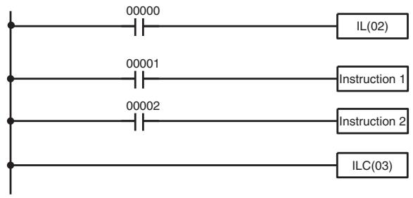
flowchart
graph TD
    A["00000"] --> B["IL(02)"]
    C["00001"] --> D["Instruction 1"]
    E["00002"] --> F["Instruction 2"]
    G["00000"] --> H["ILC(03)"]
| Address | Instruction | Operands |
| 00000 | LD | 00000 |
| 00001 | IL(02) | --- |
| 00002 | LD | 00001 |
| 00003 | Instruction 1 | |
| 00004 | LD | 00002 |
| 00005 | Instruction 2 | |
| 00006 | ILC(03) | --- |
If IR 00000 is ON in the revised version of diagram B, above, the status of IR 00001 and that of IR 00002 would determine the execution conditions for instructions 1 and 2, respectively. Because IR 00000 is ON, this would produce the same results as ANDing the status of each of these bits. If IR 00000 is OFF, the INTERLOCK instruction would produce an OFF execution condition for instructions 1 and 2 and then execution would continue with the instruction line following the INTERLOCK CLEAR instruction.
As shown in the following diagram, more than one INTERLOCK instruction can be used within one instruction block; each is effective through the next INTERLOCK CLEAR instruction.
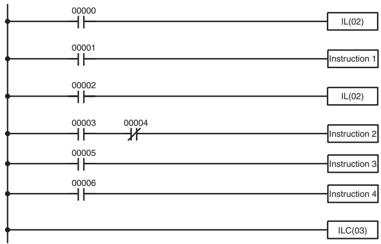
flowchart
graph TD
    A["00000"] --> B["IL(02)"]
    C["00001"] --> D["Instruction 1"]
    E["00002"] --> F["IL(02)"]
    G["00003"] --> H["Instruction 2"]
    I["00005"] --> J["Instruction 3"]
    K["00006"] --> L["Instruction 4"]
    M["ILC(03)"] --> N["Instruction 4"]
| Address | Instruction | Operands |
| 00000 | LD | 00000 |
| 00001 | IL(02) | --- |
| 00002 | LD | 00001 |
| 00003 | Instruction 1 | |
| 00004 | LD | 00002 |
| 00005 | IL(02) | --- |
| 00006 | LD | 00003 |
| 00007 | AND NOT | 00004 |
| 00008 | Instruction 2 | |
| 00009 | LD | 00005 |
| 00010 | Instruction 3 | |
| 00011 | LD | 00006 |
| 00012 | Instruction 4 | |
| 00013 | ILC(03) | --- |
If IR 00000 in the above diagram is OFF (i.e., if the execution condition for the first INTERLOCK instruction is OFF), instructions 1 through 4 would be executed with OFF execution conditions and execution would move to the instruction following the INTERLOCK CLEAR instruction. If IR 00000 is ON, the status of IR 00001 would be loaded as the execution condition for instruction 1 and then the status of IR 00002 would be loaded to form the execution condition for the second INTERLOCK instruction. If IR 00002 is OFF, instructions 2 through 4 will be executed with OFF execution conditions. If IR 00002 is ON, IR 00003, IR 00005, and IR 00006 will determine the first execution condition in new instruction lines.
4-3-9 Jumps
A specific section of a program can be skipped according to a designated execution condition. Although this is similar to what happens when the execution condition for an INTERLOCK instruction is OFF, with jumps, the operands for all instructions maintain status. Jumps can therefore be used to control devices that require a sustained output, e.g., pneumatics and hydraulics, whereas interlocks can be used to control devices that do not required a sustained output, e.g., electronic instruments.
Jumps are created using the JUMP (JMP(04)) and JUMP END (JME(05)) instructions. If the execution condition for a JUMP instruction is ON, the program is executed normally as if the jump did not exist. If the execution condition for the JUMP instruction is OFF, program execution moves immediately to a JUMP END instruction without changing the status of anything between the JUMP and JUMP END instruction.
All JUMP and JUMP END instructions are assigned jump numbers ranging between 00 and 99. There are two types of jumps. The jump number used determines the type of jump.
A jump can be defined using jump numbers 01 through 99 only once, i.e., each of these numbers can be used once in a JUMP instruction and once in a JUMP END instruction. When a JUMP instruction assigned one of these numbers is executed, execution moves immediately to the JUMP END instruction that has the same number as if all of the instruction between them did not exist. Diagram B from the TR bit and interlock example could be redrawn as shown below using a jump. Although 01 has been used as the jump number, any number between 01 and 99 could be used as long as it has not already been used in a different part of the program. JUMP and JUMP END require no other operand and JUMP END never has conditions on the instruction line leading to it.
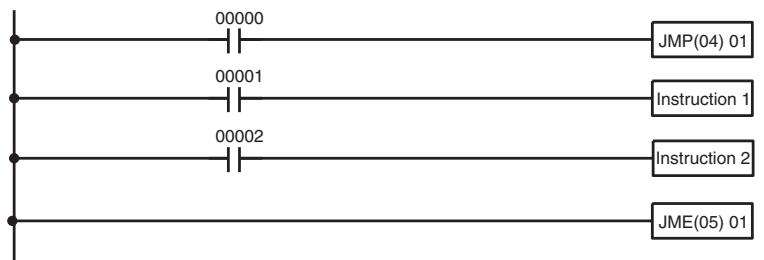
flowchart
graph TD
    A["00000"] --> B["JMP(04) 01"]
    C["00001"] --> D["Instruction 1"]
    E["00002"] --> F["Instruction 2"]
    G["JME(05) 01"] --> H["End"]
Diagram B: Corrected with a Jump
| Address | Instruction | Operands |
| 00000 | LD | 00000 |
| 00001 | JMP(04) | 01 |
| 00002 | LD | 00001 |
| 00003 | Instruction 1 | |
| 00004 | LD | 00002 |
| 00005 | Instruction 2 | |
| 00006 | JME(05) | 01 |
This version of diagram B would have a shorter execution time when IR 00000 was OFF than any of the other versions.
The other type of jump is created with a jump number of 00. As many jumps as desired can be created using jump number 00 and JUMP instructions using 00 can be used consecutively without a JUMP END using 00 between them. It is even possible for all JUMP 00 instructions to move program execution to the same JUMP END 00, i.e., only one JUMP END 00 instruction is required for all JUMP 00 instruction in the program. When 00 is used as the jump number for a JUMP instruction, program execution moves to the instruction following the next JUMP END instruction with a jump number of 00. Although, as in all jumps, no status is changed and no instructions are executed between the JUMP 00 and JUMP END 00 instructions, the program must search for the next JUMP END 00 instruction, producing a slightly longer execution time.
Execution of programs containing multiple JUMP 00 instructions for one JUMP END 00 instruction is similar to that of interlocked sections. The following diagram is the same as that used for the interlock example above, except redrawn with jumps. The execution of this diagram would differ from that of the diagram described above (e.g., in the previous diagram interlocks would reset certain parts of the interlocked section, however, jumps do not affect the status of any bit between the JUMP and JUMP END instructions).
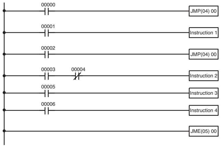
flowchart
graph TD
    A["00000"] --> B["JMP(04) 00"]
    C["00001"] --> D["Instruction 1"]
    E["00002"] --> F["JMP(04) 00"]
    G["00003"] --> H["00004"]
    I["00005"] --> J["Instruction 2"]
    K["00006"] --> L["Instruction 3"]
    M["Instruction 4"] --> N["JME(05) 00"]
| Address | Instruction | Operands |
| 00000 | LD | 00000 |
| 00001 | JMP(04) | 00 |
| 00002 | LD | 00001 |
| 00003 | Instruction 1 | |
| 00004 | LD | 00002 |
| 00005 | JMP(04) | 00 |
| 00006 | LD | 00003 |
| 00007 | AND NOT | 00004 |
| 00008 | Instruction 2 | |
| 00009 | LD | 00005 |
| 00010 | Instruction 3 | |
| 00011 | LD | 00006 |
| 00012 | Instruction 4 | |
| 00013 | JME(05) | 00 |
4-4 Controlling Bit Status
There are seven basic instructions that can be used generally to control individual bit status. These are the OUTPUT, OUTPUT NOT, SET, RESET, DIFFERENTIATE UP, DIFFERENTIATE DOWN, and KEEP instructions. All of these instructions appear as the last instruction in an instruction line and take a bit address for an operand. Although details are provided in 5-9 Bit Control Instructions, these instructions (except for OUTPUT and OUTPUT NOT, which have already been introduced) are described here because of their importance in most programs. Although these instructions are used to turn ON and OFF output bits in the IR area (i.e., to send or stop output signals to external devices), they are also used to control the status of other bits in the IR area or in other data areas.
4-4-1 SET and RESET
The SET and RESET instructions are very similar to the OUTPUT and OUTPUT NOT instructions except that they only change the status of their operand bits for ON execution conditions. Neither instructions will affect the status of its operand bit when the execution condition is OFF.
SET will turn ON the operand bit when the execution condition goes ON, but unlike the OUTPUT instruction, SET will not turn OFF the operand bit when the execution condition goes OFF. RESET will turn OFF the operand bit when the execution condition goes OFF, but unlike OUTPUT NOT, RESET will not turn ON the operand bit when the execution condition goes OFF.
In the following example, IR 10000 will be turned ON when IR 00100 goes ON and will remain ON until IR 00101 goes ON, regardless of the status of IR 00100. When IR 00101 goes ON, RESET will turn IR 10000 OFF.
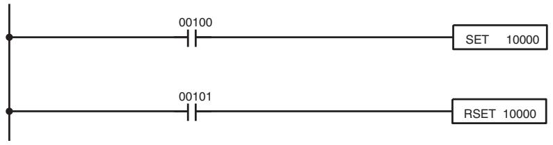
| Address | Instruction | Operands |
| 00000 | LD | 00100 |
| 00001 | SET | 10000 |
| 00002 | LD | 00101 |
| 00003 | RSET | 10000 |
4-4-2 DIFFERENTIATE UP and DIFFERENTIATE DOWN
DIFFERENTIATE UP and DIFFERENTIATE DOWN instructions are used to turn the operand bit ON for one cycle at a time. The DIFFERENTIATE UP instruction turns ON the operand bit for one cycle after the execution condition for it goes from OFF to ON; the DIFFERENTIATE DOWN instruction turns ON the operand bit for one cycle after the execution condition for it goes from ON to OFF. Both of these instructions require only one line of mnemonic code.
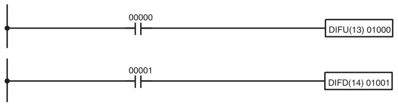
| Address | Instruction | Operands |
| 00000 | LD | 00000 |
| 00001 | DIFU(13) | 01000 |
| Address | Instruction | Operands |
| 00000 | LD | 00001 |
| 00001 | DIFD(14) | 01001 |
Here, IR 01000 will be turned ON for one cycle after IR 00000 goes ON. The next time DIFU(13) 01000 is executed, IR 01000 will be turned OFF, regardless of the status of IR 00000. With the DIFFERENTIATE DOWN instruction, IR 01001 will be turned ON for one cycle after IR 00001 goes OFF (IR 01001 will be kept OFF until then), and will be turned OFF the next time DIFD(14) 01001 is executed.
4-4-3 KEEP
The KEEP instruction is used to maintain the status of the operand bit based on two execution conditions. To do this, the KEEP instruction is connected to two instruction lines. When the execution condition at the end of the first instruction line is ON, the operand bit of the KEEP instruction is turned ON. When the execution condition at the end of the second instruction line is ON, the operand bit of the KEEP instruction is turned OFF. The operand bit for the KEEP instruction will maintain its ON or OFF status even if it is located in an interlocked section of the diagram.
In the following example, HR 0000 will be turned ON when IR 00002 is ON and IR 00003 is OFF. HR 0000 will then remain ON until either IR 00004 or IR 00005 turns ON. With KEEP, as with all instructions requiring more than one instruction line, the instruction lines are coded first before the instruction that they control.
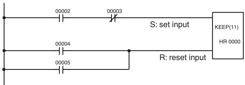
| Address | Instruction | Operands |
| 00000 | LD | 00002 |
| 00001 | AND NOT | 00003 |
| 00002 | LD | 00004 |
| 00003 | OR | 00005 |
| 00004 | KEEP(11) | HR 0000 |
4-4-4 Self-maintaining Bits (Seal)
Although the KEEP instruction can be used to create self-maintaining bits, it is sometimes necessary to create self-maintaining bits in another way so that they can be turned OFF when in an interlocked section of a program.
To create a self-maintaining bit, the operand bit of an OUTPUT instruction is used as a condition for the same OUTPUT instruction in an OR setup so that the operand bit of the OUTPUT instruction will remain ON or OFF until
changes occur in other bits. At least one other condition is used just before the OUTPUT instruction to function as a reset. Without this reset, there would be no way to control the operand bit of the OUTPUT instruction.
The above diagram for the KEEP instruction can be rewritten as shown below. The only difference in these diagrams would be their operation in an interlocked program section when the execution condition for the INTERLOCK instruction was ON. Here, just as in the same diagram using the KEEP instruction, two reset bits are used, i.e., HR 0000 can be turned OFF by turning ON either IR 00004 or IR 00005.
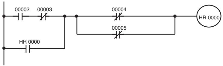
| Address | Instruction | Operands |
| 00000 | LD | 00002 |
| 00001 | AND NOT | 00003 |
| 00002 | OR | HR 0000 |
| 00003 | AND NOT | 00004 |
| 00004 | OR NOT | 00005 |
| 00005 | OUT | HR 0000 |
4-5 Work Bits (Internal Relays)
In programming, combining conditions to directly produce execution conditions is often extremely difficult. These difficulties are easily overcome, however, by using certain bits to trigger other instructions indirectly. Such programming is achieved by using work bits. Sometimes entire words are required for these purposes. These words are referred to as work words.
Work bits are not transferred to or from the PC. They are bits selected by the programmer to facilitate programming as described above. I/O bits and other dedicated bits cannot be used as works bits. All bits in the IR area that are not allocated as I/O bits, and certain unused bits in the AR area, are available for use as work bits. Be careful to keep an accurate record of how and where you use work bits. This helps in program planning and writing, and also aids in debugging operations.
Work Bit Applications
Examples given later in this subsection show two of the most common ways to employ work bits. These should act as a guide to the almost limitless number of ways in which the work bits can be used. Whenever difficulties arise in programming a control action, consideration should be given to work bits and how they might be used to simplify programming.
Work bits are often used with the OUTPUT, OUTPUT NOT, DIFFERENTIATE UP, DIFFERENTIATE DOWN, and KEEP instructions. The work bit is used first as the operand for one of these instructions so that later it can be used as a condition that will determine how other instructions will be executed. Work bits can also be used with other instructions, e.g., with the SHIFT REGISTER instruction (SFT(10)). An example of the use of work words and bits with the SHIFT REGISTER instruction is provided in 5-17-1 SHIFT REGISTER - SFT(10).
Although they are not always specifically referred to as work bits, many of the bits used in the examples in SECTION 5 Instruction Set use work bits. Understanding the use of these bits is essential to effective programming.
Reducing Complex Conditions
Work bits can be used to simplify programming when a certain combination of conditions is repeatedly used in combination with other conditions. In the following example, IR 00000, IR 00001, IR 00002, and IR 00003 are combined in a logic block that stores the resulting execution condition as the status of IR 21600. IR 21600 is then combined with various other conditions to deter-
mine output conditions for IR 10000, IR 10001, and IR 10002, i.e., to turn the outputs allocated to these bits ON or OFF.
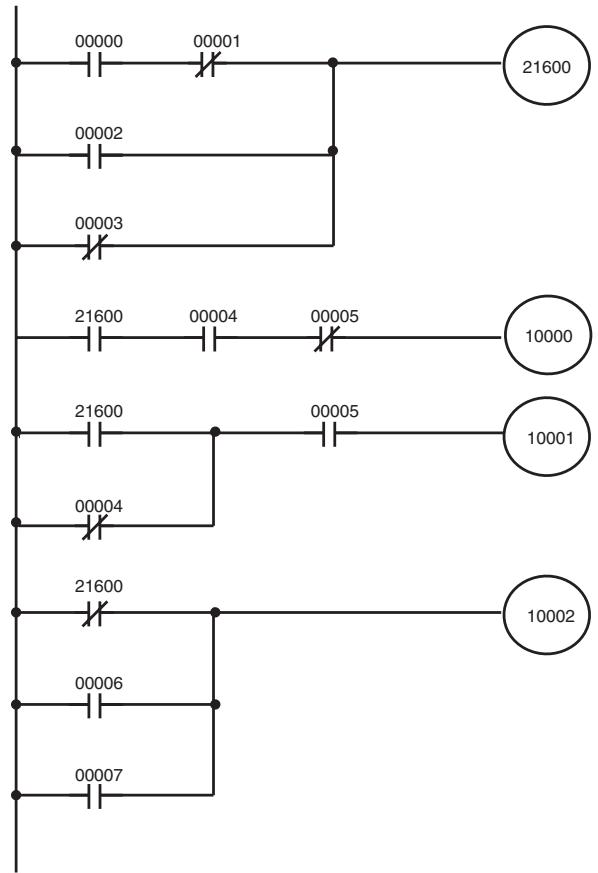
flowchart
graph TD
    A["00000"] --> B["00001"]
    C["00002"] --> D["00003"]
    E["21600"] --> F["00004"]
    G["21600"] --> H["00005"]
    I["21600"] --> J["00006"]
    K["21600"] --> L["10000"]
    M["21600"] --> N["10001"]
    O["21600"] --> P["10002"]
| Address | Instruction | Operands |
| 00000 | LD | 00000 |
| 00001 | AND NOT | 00001 |
| 00002 | OR | 00002 |
| 00003 | OR NOT | 00003 |
| 00004 | OUT | 21600 |
| 00005 | LD | 21600 |
| 00006 | AND | 00004 |
| 00007 | AND NOT | 00005 |
| 00008 | OUT | 10000 |
| 00009 | LD | 21600 |
| 00010 | OR NOT | 00004 |
| 00011 | AND | 00005 |
| 00012 | OUT | 10001 |
| 00013 | LD NOT | 21600 |
| 00014 | OR | 00006 |
| 00015 | OR | 00007 |
| 00016 | OUT | 10002 |
Differentiated Conditions
Work bits can also be used if differential treatment is necessary for some, but not all, of the conditions required for execution of an instruction. In this example, IR 10000 must be left ON continuously as long as IR 001001 is ON and both IR 00002 and IR 00003 are OFF, or as long as IR 00004 is ON and IR 00005 is OFF. It must be turned ON for only one cycle each time IR 00000 turns ON (unless one of the preceding conditions is keeping it ON continuously).
This action is easily programmed by using IR 22500 as a work bit as the operand of the DIFFERENTIATE UP instruction (DIFU(13)). When IR 00000 turns ON, IR 22500 will be turned ON for one cycle and then be turned OFF the next cycle by DIFU(13). Assuming the other conditions controlling IR 10000 are not keeping it ON, the work bit IR 22500 will turn IR 10000 ON for one cycle only.
| Address | Instruction | Operands |
| 00000 | LD | 00000 |
| 00001 | DIFU(13) | 22500 |
| 00002 | LD | 22500 |
| 00003 | LD | 00001 |
| 00004 | AND NOT | 00002 |
| 00005 | AND NOT | 00003 |
| 00006 | OR LD | --- |
| 00007 | LD | 00004 |
| 00008 | AND NOT | 00005 |
| 00009 | OR LD | --- |
| 00010 | OUT | 10000 |
4-6 Programming Precautions
The number of conditions that can be used in series or parallel is unlimited as long as the memory capacity of the PC is not exceeded. Therefore, use as many conditions as required to draw a clear diagram. Although very complicated diagrams can be drawn with instruction lines, there must not be any conditions on lines running vertically between two other instruction lines. Diagram A shown below, for example, is not possible, and should be drawn as diagram B. Mnemonic code is provided for diagram B only; coding diagram A would be impossible.
Diagram A: Not Programmable
flowchart
graph TD
    A["00001"] --> B["00004"]
    C["00000"] --> D["00004"]
    E["00000"] --> F["00004"]
    G["00001"] --> H["00003"]
    I["00002"] --> J["Instruction 1"]
    K["00003"] --> L["Instruction 2"]
Diagram B: Correct Version
| Address | Instruction | Operands |
| 00000 | LD | 00001 |
| 00001 | AND | 00004 |
| 00002 | OR | 00000 |
| 00003 | AND | 00002 |
| 00004 | Instruction 1 | |
| 00005 | LD | 00000 |
| 00006 | AND | 00004 |
| 00007 | OR | 00001 |
| 00008 | AND NOT | 00003 |
| 00009 | Instruction 2 |
The number of times any particular bit can be assigned to conditions is not limited, so use them as many times as required to simplify your program. Often, complicated programs are the result of attempts to reduce the number of times a bit is used.
Except for instructions for which conditions are not allowed (e.g., INTERLOCK CLEAR and JUMP END, see below), every instruction line must also have at least one condition on it to determine the execution condition for the instruction at the right. Again, diagram A, below, must be drawn as diagram B. If an instruction must be continuously executed (e.g., if an output must always be kept ON while the program is being executed), the Always ON Flag (SR 25313) in the SR area can be used.
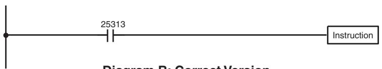
Diagram B: Correct Version
| Address | Instruction | Operands |
| 00000 | LD | 25313 |
| 00001 | Instruction |
There are a few exceptions to this rule, including the INTERLOCK CLEAR, JUMP END, and step instructions. Each of these instructions is used as the second of a pair of instructions and is controlled by the execution condition of the first of the pair. Conditions should not be placed on the instruction lines leading to these instructions. Refer to SECTION 5 Instruction Set for details.
When drawing ladder diagrams, it is important to keep in mind the number of instructions that will be required to input it. In diagram A, below, an OR LOAD instruction will be required to combine the top and bottom instruction lines. This can be avoided by redrawing as shown in diagram B so that no AND LOAD or OR LOAD instructions are required. Refer to 5-8-2 AND LOAD and OR LOAD for more details.
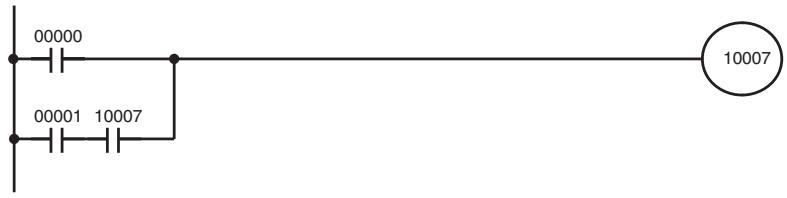
Diagram A
| Address | Instruction | Operands |
| 00000 | LD | 00000 |
| 00001 | LD | 00001 |
| 00002 | AND | 10007 |
| 00003 | OR LD | --- |
| 00004 | OUT | 10007 |
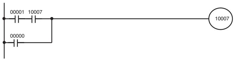
Diagram B
| Address | Instruction | Operands |
| 00000 | LD | 00001 |
| 00001 | AND | 10007 |
| 00002 | OR | 00000 |
| 00003 | OUT | 10007 |
4-7 Program Execution
When program execution is started, the CPU Unit scans the program from top to bottom, checking all conditions and executing all instructions accordingly as it moves down the bus bar. It is important that instructions be placed in the proper order so that, for example, the desired data is moved to a word before that word is used as the operand for an instruction. Remember that an instruction line is completed to the terminal instruction at the right before executing an instruction lines branching from the first instruction line to other terminal instructions at the right.
Program execution is only one of the tasks carried out by the CPU Unit as part of the cycle time. Refer to SECTION 7 CPU Unit Operation and Processing Time for details.
4-8 Indirectly Addressing the DM and EM Areas
The DM and EM areas can be addressed either directly or indirectly. Indirect addresses are indicated using an asterisk before the address, e.g., *DM 0000.
Direct Addresses
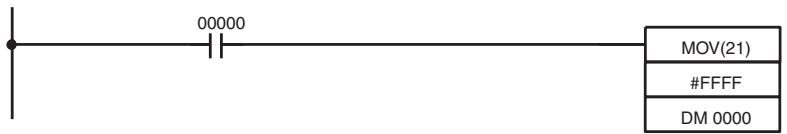
When IR 00000 is ON, the constant FFFF is moved to DM 0000.

Indirect Addresses
With indirect addresses, the contents of the address given in the operand is treated as BCD and used as the final address in the EM or DM area.
flowchart
graph LR
    A["00000"] --> B["MOV(21)"]
    A --> C["#FFFF"]
    A --> D["*DM 0000"]
When IR 00000 is ON, the constant FFFF is moved to the address specified in DM 0000, i.e., DM 0123.
flowchart
graph TD
    A["DM 0000"] --> B["0123"]
    C["DM 0123"] --> D["#FFFF"]
    E["#FFFF"] --> F["Arrow pointing to the next block"]
    style A fill:#f9f,stroke:#333
    style B fill:#ccf,stroke:#333
    style C fill:#cfc,stroke:#333
    style D fill:#fcc,stroke:#333
    style E fill:#ffc,stroke:#333
    style F fill:#fcc,stroke:#333
Note The contents of a word used as an indirect must be BCD and must not exceed the addressing range of the DM or EM area. If it is not BCD, a BCD error will occur. If the DM or EM area is exceeded, an indirect addressing error will occur. The Error Flag (SR 25503) will turn ON for either of these errors and the instruction will not be executed.
SECTION 5
Instruction Set
The CQM1H has a large programming instruction set that allows for easy programming of complicated control processes. This section explains instructions individually and provides the ladder diagram symbol, data areas, and flags used with each.
The many instructions provided by these PCs are organized in the following subsections by instruction group. These groups include Ladder Diagram Instructions, instructions with fixed function codes, and set instructions.
Some instructions, such as Timer and Counter instructions, are used to control execution of other instructions, e.g., a TIM Completion Flag might be used to turn ON a bit when the time period set for the timer has expired. Although these other instructions are often used to control output bits through the Output instruction, they can be used to control execution of other instructions as well. The Output instructions used in examples in this manual can therefore generally be replaced by other instructions to modify the program for specific applications other than controlling output bits directly.
5-1 Notation.... 211
5-2 Instruction Format.... 211
5-3 Data Areas, Definer Values, and Flags 211
5-4 Differentiated Instructions 213
5-5 Expansion Instructions 214
5-6 Coding Right-hand Instructions 215
5-7 Instruction Tables 217
5-7-1 Instructions with Fixed Function Codes.... 217
5-7-2 Expansion Instructions 218
5-7-3 Alphabetic List by Mnemonic 218
5-8 Ladder Diagram Instructions 222
5-8-1 LOAD, LOAD NOT, AND, AND NOT, OR, and OR NOT..... 222
5-8-2 AND LOAD and OR LOAD 223
5-9 Bit Control Instructions.... 223
5-9-1 OUTPUT and OUTPUT NOT – OUT and OUT NOT. 224
5-9-2 SET and RESET – SET and RSET.... 224
5-9-3 KEEP - KEEP(11) 225
5-9-4 DIFFERENTIATE UP and DOWN - DIFU(13) and DIFD(14) ... 226
5-17 Shift Instructions 261
5-17-1 SHIFT REGISTER - SFT(10) 261
5-17-2 WORD SHIFT - WSFT(16) 262
5-17-3 ARITHMETIC SHIFT LEFT - ASL(25) 263
5-17-4 ARITHMETIC SHIFT RIGHT - ASR(26) 263
5-17-5 ROTATE LEFT - ROL(27) 264
5-17-6 ROTATE RIGHT - ROR(28) 264
5-17-7 ONE DIGIT SHIFT LEFT - SLD(74) 265
5-17-8 ONE DIGIT SHIFT RIGHT - SRD(75).... 266
5-17-9 REVERSIBLE SHIFT REGISTER - SFTR(84) 266
5-17-10 ASYNCHRONOUS SHIFT REGISTER - ASFT(17) 268
5-18 Data Movement Instructions 269
5-18-1 MOVE-MOV(21) 269
5-18-2 MOVE NOT-MVN(22) 270
5-18-3 BLOCK TRANSFER - XFER(70) 271
5-18-4 BLOCK SET - BSET(71).... 272
5-18-5 DATA EXCHANGE – XCHG(73) 273
5-18-6 SINGLE WORD DISTRIBUTE - DIST(80) 273
5-18-7 DATA COLLECT - COLL(81).... 275
5-18-8 MOVE BIT - MOVB(82) 277
5-18-9 MOVE DIGIT - MOVD(83).... 278
5-18-10 TRANSFER BITS - XFRB(—) 279
5-19 Comparison Instructions 280
5-19-1 COMPARE-CMP(20).... 280
5-19-2 TABLE COMPARE - TCMP(85).... 282
5-19-3 BLOCK COMPARE - BCMP(68) 283
5-19-4 DOUBLE COMPARE - CMPL(60) 284
5-19-5 MULTI-WORD COMPARE - MCMP(19) 285
5-19-6 SIGNED BINARY COMPARE - CPS(—). 286
5-19-7 DOUBLE SIGNED BINARY COMPARE - CPSL(—)....287
5-19-8 AREA RANGE COMPARE - ZCP(--) 289
5-19-9 DOUBLE AREA RANGE COMPARE - ZCPL(—) 290
5-20 Conversion Instructions 291
5-20-1 BCD-TO-BINARY - BIN(23) 291
5-20-2 BINARY-TO-BCD - BCD(24) 292
5-20-3 DOUBLE BCD-TO-DOUBLE BINARY - BINL(58) 293
5-20-4 DOUBLE BINARY-TO-DOUBLE BCD - BCDL(59) 293
5-20-5 4-TO-16 DECODER - MLPX(76) 294
5-20-6 16-TO-4 ENCODER - DMPX(77).... 296
5-20-7 7-SEGMENT DECODER - SDEC(78) 298
5-20-8 ASCII CONVERT - ASC(86) 301
5-20-9 ASCII-TO-HEXADECIMAL - HEX(—) 303
5-20-10 SCALING-SCL(66) 305
5-20-11 SIGNED BINARY TO BCD SCALING - SCL2(—) 307
5-20-12 BCD TO SIGNED BINARY SCALING - SCL3(—) 308
5-20-13 HOURS-TO-SECONDS - SEC(—) 311
5-20-14 SECONDS-TO-HOURS - HMS(—) 312
5-20-15 COLUMN-TO-LINE - LINE(—).... 313
5-20-16 LINE-TO-COLUMN - COLM(—) 314
5-20-17 2'S COMPLEMENT - NEG(—) 315
5-20-18 DOUBLE 2'S COMPLEMENT - NEGL(—) 316
5-21 BCD Calculation Instructions 317
5-21-1 SET CARRY - STC(40).... 317
5-21-2 CLEAR CARRY - CLC(41) 317
5-21-3 BCD ADD - ADD(30) 317
5-21-4 BCD SUBTRACT - SUB(31) 318
5-21-5 BCD MULTIPLY - MUL(32) 320
5-21-6 BCD DIVIDE - DIV(33) 321
5-21-7 DOUBLE BCD ADD - ADDL(54) 322
5-21-8 DOUBLE BCD SUBTRACT - SUBL(55) 324
5-21-9 DOUBLE BCD MULTIPLY - MULL(56) 325
5-21-10 DOUBLE BCD DIVIDE -DIVL(57) 326
5-21-11 SQUARE ROOT - ROOT(72) 327
5-22 Binary Calculation Instructions 328
5-22-1 BINARY ADD - ADB(50).... 328
5-22-2 BINARY SUBTRACT - SBB(51) 329
5-22-3 BINARY MULTIPLY - MLB(52) 330
5-22-4 BINARY DIVIDE - DVB(53) 331
5-22-5 DOUBLE BINARY ADD - ADBL(—).... 332
5-22-6 DOUBLE BINARY SUBTRACT - SBBL(--) 333
5-22-7 SIGNED BINARY MULTIPLY - MBS(—) 334
5-22-8 DOUBLE SIGNED BINARY MULTIPLY - MBSL(—) 335
5-22-9 SIGNED BINARY DIVIDE - DBS(—) 336
5-22-10 DOUBLE SIGNED BINARY DIVIDE - DBSL(—).... 337
5-23 Special Math Instructions 338
5-24 Floating-point Math Instructions 347
5-24-1 FLOATING TO 16-BIT: FIX(—)....352
5-24-2 FLOATING TO 32-BIT: FIXL(—) 353
5-24-3 16-BIT TO FLOATING: FLT(—) 354
5-24-4 32-BIT TO FLOATING: FLTL(—) 355
5-24-5 FLOATING-POINT ADD: +F(—).... 355
5-24-6 FLOATING-POINT SUBTRACT: -F(—) 357
5-24-7 FLOATING-POINT MULTIPLY: *F(—) 358
5-24-8 FLOATING-POINT DIVIDE: /F(—).... 359
5-24-9 DEGREES TO RADIANS: RAD(—) 360
5-24-10 RADIANS TO DEGREES: DEG(—) 361
5-24-11 SINE: SIN(—) 362
5-24-12 COSINE: COS(—) 363
5-24-13 TANGENT: TAN(-) 364
5-24-14 ARC SINE: ASIN(—) 365
5-24-15 ARC COSINE: ACOS(—) 366
5-24-16 ARC TANGENT: ATAN(—) 367
5-24-17 SQUARE ROOT: SQRT(—) 369
5-24-18 EXPONENT: EXP(—).... 370
5-24-19 LOGARITHM: LOG(—) 371
5-25 Logic Instructions 372
5-25-1 COMPLEMENT - COM(29) 372
5-25-2 LOGICAL AND - ANDW(34).... 373
5-25-3 LOGICAL OR - ORW(35) 374
5-25-4 EXCLUSIVE OR - XORW(36) 374
5-25-5 EXCLUSIVE NOR - XNRW(37).... 375
5-26 Increment/Decrement Instructions.... 376
5-26-1 BCD INCREMENT - INC(38).... 376
5-26-2 BCD DECREMENT - DEC(39).... 376
5-27 Subroutine Instructions 377
5-27-1 SUBROUTINE ENTER - SBS(91) 377
5-27-2 SUBROUTINE DEFINE and RETURN - SBN(92)/RET(93).... 379
5-28 Special Instructions 379
5-28-1 TRACE MEMORY SAMPLING – TRSM(45) 379
5-28-2 MESSAGE DISPLAY - MSG(46) 381
5-28-3 I/O REFRESH - IORF(97) 382
5-28-4 MACRO-MCRO(99) 383
5-28-5 BIT COUNTER - BCNT(67) 385
5-28-6 FRAME CHECKSUM - FCS(--) 385
5-28-7 FAILURE POINT DETECTION - FPD(—) 387
5-28-8 INTERRUPT CONTROL - INT(89) 391
5-28-9 SET PULSES - PULS(65) 393
5-28-10 SPEED OUTPUT- SPED(64) 395
5-28-11 PULSE OUTPUT - PLS2(—) 398
5-28-12 ACCELERATION CONTROL - ACC(—) 400
5-28-13 PULSE WITH VARIABLE DUTY FACTOR - PWM(—) ..... 402
5-28-14 DATA SEARCH - SRCH(—).... 403
5-28-15 PID CONTROL - PID(—) 405
5-29 Network Instructions 406
5-29-1 NETWORK SEND - SEND(90) 406
5-29-2 NETWORK RECEIVE - RECV(98) 410
5-29-3 DELIVER COMMAND: CMND(—). 412
5-30 Communications Instructions 415
5-30-1 RECEIVE-RXD(47) 415
5-30-2 TRANSMIT-TXD(48) 417
5-30-3 CHANGE SERIAL PORT SETUP - STUP(—). 419
5-30-4 PROTOCOL MACRO - PMCR(—) 422
5-31 Advanced I/O Instructions.... 424
5-31-1 7-SEGMENT DISPLAY OUTPUT - 7SEG(88) 424
5-31-2 DIGITAL SWITCH INPUT - DSW(87) 427
5-31-3 HEXADECIMAL KEY INPUT - HKY(—) 431
5-31-4 TEN KEY INPUT - TKY(18) 434
5-1 Notation
In the remainder of this manual, all instructions will be referred to by their mnemonics. For example, the OUTPUT instruction will be called OUT; the AND LOAD instruction, AND LD. If you're not sure of the instruction a mnemonic is used for, refer to Appendix A Programming Instructions.
If an instruction is assigned a function code, it will be given in parentheses after the mnemonic. These function codes, which are 2-digit decimal numbers, are used to input most instructions into the CPU Unit. A table of instructions listed in order of function codes is also provided in Appendix A Programming Instructions. Lists of instructions are also provided in 5-7 Instruction Tables.
An @ before a mnemonic indicates the differentiated version of that instruction. Differentiated instructions are explained in Section 5-4.
5-2 Instruction Format
Most instructions have at least one or more operands associated with them. Operands indicate or provide the data on which an instruction is to be performed. These are sometimes input as the actual numeric values (i.e., as constants), but are usually the addresses of data area words or bits that contain the data to be used. A bit whose address is designated as an operand is called an operand bit; a word whose address is designated as an operand is called an operand word. In some instructions, the word address designated in an instruction indicates the first of multiple words containing the desired data.
Each instruction requires one or more words in Program Memory. The first word is the instruction word, which specifies the instruction and contains any definers (described below) or operand bits required by the instruction. Other operands required by the instruction are contained in following words, one operand per word. Some instructions require up to four words.
A definer is an operand associated with an instruction and contained in the same word as the instruction itself. These operands define the instruction rather than telling what data it is to use. Examples of definers are TIM/CNT numbers, which are used in timer and counter instructions to create timers and counters, as well as jump numbers (which define which Jump instruction is paired with which Jump End instruction). Bit operands are also contained in the same word as the instruction itself, although these are not considered definers.
5-3 Data Areas, Definer Values, and Flags
In this section, each instruction description includes its ladder diagram symbol, the data areas that can be used by its operands, and the values that can be used as definers. Details for the data areas are also specified by the operand names and the type of data required for each operand (i.e., word or bit and, for words, hexadecimal or BCD).
Not all addresses in the specified data areas are necessarily allowed for an operand, e.g., if an operand requires two words, the last word in a data area cannot be designated as the first word of the operand because all words for a single operand must be within the same data area. Other specific limitations are given in a Limitations subsection. Refer to SECTION 3 Memory Areas for addressing conventions and the addresses of flags and control bits.
Caution
The IR and SR areas are considered as separate data areas. If an operand has access to one area, it doesn't necessarily mean that the same operand will have access to the other area. The border between the IR and SR areas
can, however, be crossed for a single operand, i.e., the last bit in the IR area may be specified for an operand that requires more than one word as long as the SR area is also allowed for that operand.
The Flags subsection lists flags that are affected by execution of an instruction. These flags include the following SR area flags.
| Abbreviation | Name | Bit |
| ER | Instruction Execution Error Flag | 25503 |
| CY | Carry Flag | 25504 |
| GR | Greater Than Flag | 25505 |
| EQ | Equals Flag | 25506 |
| LE | Less Than Flag | 25507 |
ER is the flag most commonly used for monitoring an instruction's execution. When ER goes ON, it indicates that an error has occurred in attempting to execute the current instruction. The Flags subsection of each instruction lists possible reasons for ER being ON. ER will turn ON if operands are not entered correctly. Instructions are not executed when ER is ON. A table of instructions and the flags they affect is provided in Appendix B Error and Arithmetic Flag Operation.
Indirect Addressing
When the DM area is specified for an operand, an indirect address can be used. Indirect DM addressing is specified by placing an asterisk before the DM: *DM.
When an indirect DM address is specified, the designated DM word will contain the address of the DM word that contains the data that will be used as the operand of the instruction. If, for example, *DM 0001 was designated as the first operand and LR 00 as the second operand of MOV(21), the contents of DM 0001 was 1111, and DM 1111 contained 5555, the value 5555 would be moved to LR 00.
flowchart
graph LR
    A["MOV(21)"] -->|Indirect address| B["Word"]
    B --> C["Content"]
    C --> D["4C59"]
    C --> E["1111"]
    C --> F["F35A"]
    B --> G["DM 0000"]
    B --> H["DM 0001"]
    B --> I["DM 0002"]
    B --> J["..."]
    B --> K["DM 1111"]
    B --> L["DM 1113"]
    B --> M["DM 1114"]
    C --> N["5555"]
    C --> O["2506"]
    C --> P["D541"]
    C --> Q["5555 moved to LR 00."]
When using indirect addressing, the address of the desired word must be in BCD and it must specify a word within the DM area. In the above example, the content of *DM 0000 would have to be in BCD between 0000 and 1999.
Designating Constants
Although data area addresses are most often given as operands, many operands and all definers are input as constants. The available value range for a given definer or operand depends on the particular instruction that uses it. Constants must also be entered in the form required by the instruction, i.e., in BCD or in hexadecimal.
5-4 Differentiated Instructions
Most instructions are provided in both differentiated and non-differentiated forms. Differentiated instructions are distinguished by an @ in front of the instruction mnemonic.
A non-differentiated instruction is executed each time it is scanned as long as its execution condition is ON. A differentiated instruction is executed only once after its execution condition goes from OFF to ON. If the execution condition has not changed or has changed from ON to OFF since the last time the instruction was scanned, the instruction will not be executed. The following two examples show how this works with MOV(21) and @MOV(21), which are used to move the data in the address designated by the first operand to the address designated by the second operand.
| Address | Instruction | Operands |
| 00000 | LD | 00000 |
| 00001 | MOV(21) | |
| HR 10 | ||
| DM 0000 |
| Address | Instruction | Operands |
| 00000 | LD | 00000 |
| 00001 | @MOV(21) | |
| HR 10 | ||
| DM 0000 |
In diagram A, the non-differentiated MOV(21) will move the content of HR 10 to DM 0000 whenever it is scanned with 00000. If the cycle time is 80 ms and 00000 remains ON for 2.0 seconds, this move operation will be performed 25 times and only the last value moved to DM 0000 will be preserved there.
In diagram B, the differentiated @MOV(21) will move the content of HR 10 to DM 0000 only once after 00000 goes ON. Even if 00000 remains ON for 2.0 seconds with the same 80 ms cycle time, the move operation will be executed only once during the first cycle in which 00000 has changed from OFF to ON. Because the content of HR 10 could very well change during the 2 seconds while 00000 is ON, the final content of DM 0000 after the 2 seconds could be different depending on whether MOV(21) or @MOV(21) was used.
All operands, ladder diagram symbols, and other specifications for instructions are the same regardless of whether the differentiated or non-differentiated form of an instruction is used. When inputting, the same function codes are also used, but NOT is input after the function code to designate the differentiated form of an instruction. Most, but not all, instructions have differentiated forms.
Refer to 5-12 INTERLOCK and INTERLOCK CLEAR - IL(02) and ILC(03) for the effects of interlocks on differentiated instructions.
The CQM1H also provides differentiation instructions: DIFU(13) and DIFD(14). DIFU(13) operates the same as a differentiated instruction, but is used to turn ON a bit for one cycle. DIFD(14) also turns ON a bit for one cycle, but does it when the execution condition has changed from ON to OFF. Refer to 5-9-4 DIFFERENTIATE UP and DOWN - DIFU(13) and DIFD(14) for details.
5-5 Expansion Instructions
A set of expansion instructions to aid in special programming needs. Function codes can be assigned to up to 18 of the expansion instructions to enable using them in programs. This allows the user to pick the instructions needed by each program to more effectively use the function codes required to input instructions.
The mnemonics of expansion instructions are followed by “(—)” as the function code to indicate that they must be assigned function codes by the user in the instructions table before they can be used in programming (unless they are used under their default settings).
Any of the instructions not assigned function codes will need to be assigned function codes by the Programming Device and the CQM1H before they can be used in programming. Changing the function codes assigned to expansion instructions will change the meaning of instructions and operands, so be sure to assign the function codes before programming and transfer the proper expansion instruction settings to the CQM1H before program execution.
Example
The following example shows how default function code settings can be changed.
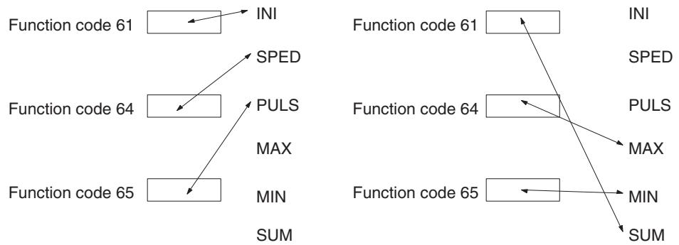
At the time of shipping, the function codes are assigned as shown above. (In this example, the instructions all relate to pulse outputs.)
If pulse outputs are not being used, and if maximum values, minimum values, and sums are required, then the Set Instructions operation can be used as shown above to re-assign instructions in the instruction table.
Function Codes for Expansion Instructions
The following 18 function codes can be used for expansion instructions: 17, 18, 19, 47, 48, 60, 61, 62, 63, 64, 65, 66, 67, 68, 69, 87, 88, and 89
The 74 expansion instructions that can be used are listed below, along with the default function codes that are assigned when the CQM1H is shipped.
| Mnemonic | Code |
| ASFT | 17 |
| TKY | 18 |
| MCMP | 19 |
| RXD | 47 |
| TXD | 48 |
| CMPL | 60 |
| INI | 61 |
| PRV | 62 |
| CTBL | 63 |
| SPED | 64 |
| PULS | 65 |
| SCL | 66 |
| BCNT | 67 |
| Mnemonic | Code |
| ACC | --- |
| ACOS | --- |
| ADBL | --- |
| APR | --- |
| ASIN | --- |
| ATAN | --- |
| AVG | --- |
| CMND | --- |
| COLM | --- |
| COS | --- |
| CPS | --- |
| CPSL | --- |
| DBS | --- |
| Mnemonic | Code |
| FIXL | --- |
| FLT | --- |
| FLTL | --- |
| FPD | --- |
| HEX | --- |
| HKY | --- |
| HMS | --- |
| LINE | --- |
| LOG | --- |
| MAX | --- |
| MBS | --- |
| MBSL | --- |
| MIN | --- |
| Mnemonic | Code |
| RAD | --- |
| SBBL | --- |
| SCL2 | --- |
| SCL3 | --- |
| SEC | --- |
| SIN | --- |
| SQRT | --- |
| SRCH | --- |
| STUP | --- |
| SUM | --- |
| TAN | --- |
| TTIM | --- |
| XFRB | --- |
| BCMP | 68 |
| STIM | 69 |
| DSW | 87 |
| 7SEG | 88 |
| INT | 89 |
| Mnemonic | Code |
| DBSL | --- |
| DEG | --- |
| EXP | --- |
| FCS | --- |
| FIX | --- |
| Mnemonic | Code |
| NEG | --- |
| NEGL | --- |
| PID | --- |
| PLS2 | --- |
| PMCR | --- |
| PWM | --- |
| Mnemonic | Code |
| ZCP | --- |
| ZCPL | --- |
| +F | --- |
| -F | --- |
| *F | --- |
| /F | --- |
The expansion instruction assignments can be stored on Memory Cassettes when they are used. Exercise care when using a Memory Cassette that has been used with another CQM1H and be sure the proper expansion instruction assignments are being used.
Caution
If pin 4 of the CQM1H's DIP switch is OFF, the default function codes will be used and user-set expansion instruction assignments will be ignored. The default function code assignments will also be set whenever power is turned on, deleting any previous settings.
Make sure that pin 4 of the CPU Unit DIP switch is ON when reading a program from the Memory Cassette that has user-set expansion instruction assignments. If pin 4 is OFF, the default function code assignments will be used for expansion instructions in programs read from a Memory Cassette. (In this case, the program read from the Memory Cassette and the program on the Memory Cassette will not match when the two are compared.)
5-6 Coding Right-hand Instructions
Writing mnemonic code for ladder instructions is described in SECTION 4 Ladder-diagram Programming. Converting the information in the ladder diagram symbol for all other instructions follows the same pattern, as described below, and is not specified for each instruction individually.
The first word of any instruction defines the instruction and provides any definers. If the instruction requires only a signal bit operand with no definer, the bit operand is also placed on the same line as the mnemonic. All other operands are placed on lines after the instruction line, one operand per line and in the same order as they appear in the ladder symbol for the instruction.
The address and instruction columns of the mnemonic code table are filled in for the instruction word only. For all other lines, the left two columns are left blank. If the instruction requires no definer or bit operand, the data column is left blank for first line. It is a good idea to cross through any blank data column spaces (for all instruction words that do not require data) so that the data column can be quickly scanned to see if any addresses have been left out.
If an IR or SR address is used in the data column, the left side of the column is left blank. If any other data area is used, the data area abbreviation is placed on the left side and the address is placed on the right side. If a constant is to be input, the number symbol (#) is placed on the left side of the data column and the number to be input is placed on the right side. Any numbers input as definers in the instruction word do not require the number symbol on the right side. TIM/CNT bits, once defined as a timer or counter, take a TIM (timer) or CNT (counter) prefix.
When coding an instruction that has a function code, be sure to write in the function code, which will be necessary when inputting the instruction via the Programming Console. Also be sure to designate the differentiated instruction with the @ symbol.
Note The mnemonics of expansion instructions are followed by “(—)” as the function code to indicate that they must be assigned function codes by the user in the instructions table before they can be used in programming. Refer to page 18 for details.
The following diagram and corresponding mnemonic code illustrates the points described above.
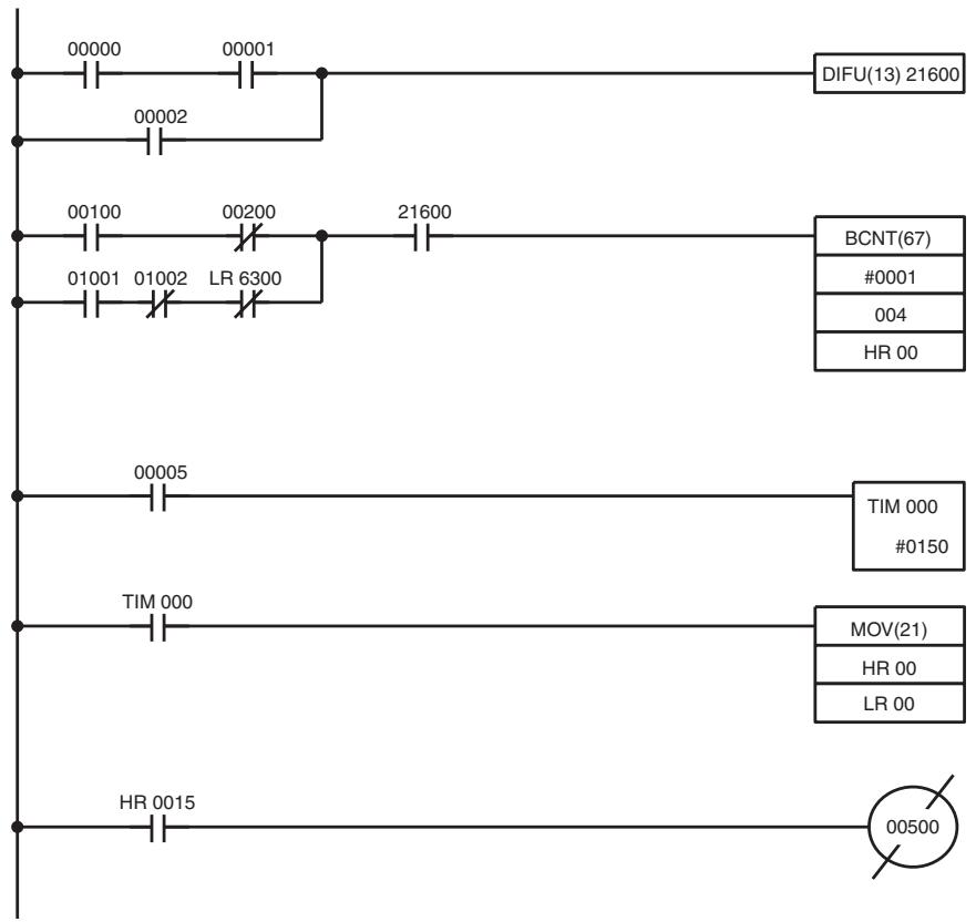
flowchart
graph TD
    A["00000"] --> B["00001"]
    C["00002"] --> D["00100"]
    E["00200"] --> F["01001"]
    G["21600"] --> H["LR 6300"]
    I["DIFU(13) 21600"] --> J["BCNT(67)"]
    K["#0001"] --> L["004"]
    M["HR 00"] --> N["TIM 000 #0150"]
    O["TIM 000"] --> P["MOV(21)"]
    Q["HR 00"] --> R["LR 00"]
    S["HR 0015"] --> T["00500"]
| Address | Instruction | Data |
| 00000 | LD | 00000 |
| 00001 | AND | 00001 |
| 00002 | OR | 00002 |
| 00003 | DIFU(13) | 21600 |
| 00004 | LD | 00100 |
| 00005 | AND NOT | 00200 |
| 00006 | LD | 01001 |
| 00007 | AND NOT | 01002 |
| 00008 | AND NOT | LR 6300 |
| 00009 | OR LD | -- |
| 00010 | AND | 21600 |
| 00011 | BCNT(67) | -- |
| # 0001 | ||
| 004 | ||
| HR 00 | ||
| 00012 | LD | 00005 |
| 00013 | TIM | 000 |
| # 0150 | ||
| 00014 | LD | TIM 000 |
| 00015 | MOV(21) | -- |
| HR 00 | ||
| LR 00 | ||
| 00016 | LD | HR 0015 |
| 00017 | OUT NOT | 00500 |
Multiple Instruction Lines
If a right-hand instruction requires multiple instruction lines (such as KEEP(11)), all of the lines for the instruction are entered before the right-hand instruction. Each of the lines for the instruction is coded, starting with LD or LD NOT, to form `logic blocks' that are combined by the right-hand instruction. An example of this for SFT(10) is shown below.
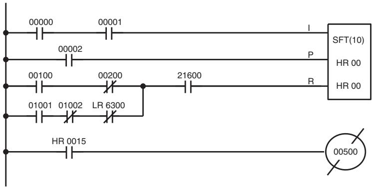
| Address | Instruction | Data |
| 00000 | LD | 00000 |
| 00001 | AND | 00001 |
| 00002 | LD | 00002 |
| 00003 | LD | 00100 |
| 00004 | AND NOT | 00200 |
| 00005 | LD | 01001 |
| 00006 | AND NOT | 01002 |
| 00007 | AND NOT | LR 6300 |
| 00008 | OR LD | — |
| 00009 | AND | 21600 |
| 00010 | SFT(10) | HR 00 |
| HR 00 | ||
| 00011 | LD | HR 0015 |
| 00012 | OUT NOT | 00500 |
5-7 Instruction Tables
This section provides tables of the instructions available in the CQM1H. The first two tables can be used to find instructions by function code. The last table can be used to find instructions by mnemonic.
5-7-1 Instructions with Fixed Function Codes
The following table lists the instructions that have fixed function codes. Each instruction is listed by mnemonic and by instruction name. Use the numbers in the leftmost column as the left digit and the number in the column heading as the right digit of the function code. The @ symbol indicates instructions with differentiated forms.
Expansion instructions without default function codes must be allocated function codes to enable using them. Even the expansion instructions with default function codes have been omitted from the following table and space has been provided so that you can write in the ones you will be using. Refer to the next page for details on expansion instructions.
| Left digit | Right digit | |||||||||
| 0 | 1 | 2 | 3 | 4 | 5 | 6 | 7 | 8 | 9 | |
| 0 | NOPNOOPERATION | ENDEND | ILINTERLOCK | ILCINTERLOCKCLEAR | JMPJUMP | JMEJUMP END | (@) FALFAILUREALARM ANDRESET | FALSSEVEREFAILUREALARM | STEPSTEPDEFINE | SNXTSTEP START |
| 1 | SFTSHIFTREGISTER | KEEPKEEP | CNTRREVERSIBLECOUNTER | DIFUDIFFERENTI-ATE UP | DIFDDIFFERENTI-ATE DOWN | TIMHHIGH-SPEEDTIMER | (@) WSFTWORD SHIFT | (ExpansionInstruction) | (ExpansionInstruction) | (ExpansionInstruction) |
| 2 | CMPCOMPARE | (@) MOVMOVE | (@) MVNMOVE NOT | (@) BINBCD TOBINARY | (@) BCDBINARY TOBCD | (@) ASLSHIFT LEFT | (@) ASRSHIFT RIGHT | (@) ROLROTATE LEFT | (@) RORROTATERIGHT | (@) COMCOMPLE-MENT |
| 3 | (@) ADDBCD ADD | (@) SUBBCDSUBTRACT | (@) MULBCDMULTIPLY | (@) DIVBCDDIVIDE | (@) ANDWLOGICALAND | (@) ORWLOGICAL OR | (@) XORWEXCLUSIVEOR | (@) XNRWEXCLUSIVENOR | (@) INCINIncrement | (@) DECDECREMENT |
| 4 | (@) STCSET CARRY | (@) CLCCLEARCARRY | --- | --- | --- | TRSMTRACE MEM-ORY SAMPLE | (@) MSGMESSAGEDISPLAY | (ExpansionInstruction) | (ExpansionInstruction) | --- |
| 5 | (@) ADB BINARY ADD | (@) SBB BINARY SUB-TRACT | (@) MLB BINARY MUL-TIPLY | (@) DVB BINARY DIVIDE | (@) ADDL DOUBLE BCD ADD | (@) SUBL DOUBLE BCD SUBTRACT | (@) MULL DOUBLE BCD MULTIPLY | (@) DIVL DOUBLE BCD DIVIDE | (@) BINL DOUBLE BCD-TO-DOUBLE BINARY | (@) BCDL DOUBLE BINARY-TO-DOUBLE BCD |
| 6 | (Expansion Instruction) | (Expansion Instruction) | (Expansion Instruction) | (Expansion Instruction) | (Expansion Instruction) | (Expansion Instruction) | (Expansion Instruction) | (Expansion Instruction) | (Expansion Instruction) | (Expansion Instruction) |
| 7 | (@) XFER BLOCK TRANSFER | (@) BSET BLOCK SET | (@) ROOT SQUARE ROOT | (@) XCHG DATA EXCHANGE | (@) SLD ONE DIGIT SHIFT LEFT | (@) SRD ONE DIGIT SHIFT RIGHT | (@) MLPX 4-TO-16 DECODER | (@) DMPX 16-TO-4 ENCODER | (@) SDEC 7-SEGMENT DECODER | --- |
| 8 | (@) DIST SINGLE WORD DISTRIBUTE | (@) COLL DATA COLLECT | (@) MOVB MOVE BIT | (@) MOVD MOVE DIGIT | (@) SFTR REVERSIBLE SHIFT REGIS-TER | (@) TCMP TABLE COMPARE | (@) ASC ASCII CONVERT | (Expansion Instruction) | (Expansion Instruction) | (Expansion Instruction) |
| 9 | (@) SEND NETWORK SEND | (@) SBS SUBROUTINE ENTRY | SBN SUBROUTINE DEFINE | RET SUBROUTINE RETURN | --- | --- | --- | (@) IORF I/O REFRESH | (@) RECV NETWORK RECEIVE | (@) MCRO MACRO |
5-7-2 Expansion Instructions
The 74 expansion instructions that can be used are listed below, along with the default function codes that are assigned when the CQM1H is shipped. Refer to 1-4 Interrupt Functions for more details.
| Mnemonic | Code |
| ASFT | 17 |
| TKY | 18 |
| MCMP | 19 |
| RXD | 47 |
| TXD | 48 |
| CMPL | 60 |
| INI | 61 |
| PRV | 62 |
| CTBL | 63 |
| SPED | 64 |
| PULS | 65 |
| SCL | 66 |
| BCNT | 67 |
| BCMP | 68 |
| STIM | 69 |
| DSW | 87 |
| 7SEG | 88 |
| INT | 89 |
| Mnemonic | Code |
| ACC | --- |
| ACOS | --- |
| ADBL | --- |
| APR | --- |
| ASIN | --- |
| ATAN | --- |
| AVG | --- |
| CMND | --- |
| COLM | --- |
| COS | --- |
| CPS | --- |
| CPSL | --- |
| DBS | --- |
| DBSL | --- |
| DEG | --- |
| EXP | --- |
| FCS | --- |
| FIX | --- |
| Mnemonic | Code |
| FIXL | --- |
| FLT | --- |
| FLTL | --- |
| FPD | --- |
| HEX | --- |
| HKY | --- |
| HMS | --- |
| LINE | --- |
| LOG | --- |
| MAX | --- |
| MBS | --- |
| MBSL | --- |
| MIN | --- |
| NEG | --- |
| NEGL | --- |
| PID | --- |
| PLS2 | --- |
| PMCR | --- |
| PWM | --- |
| Mnemonic | Code |
| RAD | --- |
| SBBL | --- |
| SCL2 | --- |
| SCL3 | --- |
| SEC | --- |
| SIN | --- |
| SQRT | --- |
| SRCH | --- |
| STUP | --- |
| SUM | --- |
| TAN | --- |
| TTIM | --- |
| XFRB | --- |
| ZCP | --- |
| ZCPL | --- |
| /F | --- |
| +F | --- |
| -F | --- |
| *F | --- |
5-7-3 Alphabetic List by Mnemonic
Dashes (“—”) in the Code column indicate expansion instructions, which do not have fixed function codes. “None” indicates instructions for which function codes are not used. The @ symbol indicates instructions with differentiated forms.
| Mnemonic | Code | Words | Name | Page |
| 7SEG | 88 | 4 | 7-SEGMENT DISPLAY OUTPUT | 424 |
| ACC (@) | — | 4 | ACCELERATION CONTROL | 400 |
| ACOS (@) | — | 3 | ARC COSINE | 366 |
| ADB (@) | 50 | 4 | BINARY ADD | 328 |
| ADBL (@) | — | 4 | DOUBLE BINARY ADD | 332 |
| ADD (@) | 30 | 4 | BCD ADD | 317 |
| ADDL (@) | 54 | 4 | DOUBLE BCD ADD | 323 |
| AND | None | 1 | AND | 222 |
| AND LD | None | 1 | AND LOAD | 223 |
| AND NOT | None | 1 | AND NOT | 222 |
| ANDW (@) | 34 | 4 | LOGICAL AND | 373 |
| APR (@) | — | 4 | ARITHMETIC PROCESS | 344 |
| ASC (@) | 86 | 4 | ASCII CONVERT | 301 |
| ASFT(@) | 17 | 4 | ASYNCHRONOUS SHIFT REGISTER | 268 |
| ASIN (@) | — | 3 | ARC SINE | 365 |
| ASL (@) | 25 | 2 | ARITHMETIC SHIFT LEFT | 263 |
| ASR (@) | 26 | 2 | ARITHMETIC SHIFT RIGHT | 263 |
| ATAN (@) | — | 3 | ARC TANGENT | 367 |
| AVG | — | 4 | AVERAGE VALUE | 341 |
| BCD (@) | 24 | 3 | BINARY TO BCD | 292 |
| BCDL (@) | 59 | 3 | DOUBLE BINARY-TO-DOUBLE BCD | 293 |
| BCMP (@) | 68 | 4 | BLOCK COMPARE | 283 |
| BCNT (@) | 67 | 4 | BIT COUNTER | 385 |
| BIN (@) | 23 | 3 | BCD-TO-BINARY | 291 |
| BINL (@) | 58 | 3 | DOUBLE BCD-TO-DOUBLE BINARY | 293 |
| BSET (@) | 71 | 4 | BLOCK SET | 272 |
| CLC (@) | 41 | 1 | CLEAR CARRY | 317 |
| CMND (@) | — | 4 | DELIVER COMMAND | 412 |
| CMP | 20 | 3 | COMPARE | 280 |
| CMPL | 60 | 4 | DOUBLE COMPARE | 284 |
| CNT | None | 2 | COUNTER | 235 |
| CNTR | 12 | 3 | REVERSIBLE COUNTER | 237 |
| COLL (@) | 81 | 4 | DATA COLLECT | 275 |
| COLM(@) | — | 4 | LINE TO COLUMN | 314 |
| COM (@) | 29 | 2 | COMPLEMENT | 372 |
| COS (@) | — | 3 | COSINE | 363 |
| CPS | — | 4 | SIGNED BINARY COMPARE | 286 |
| CPSL | — | 4 | DOUBLE SIGNED BINARY COMPARE | 287 |
| CTBL(@) | 63 | 4 | COMPARISON TABLE LOAD | 243 |
| DBS (@) | — | 4 | SIGNED BINARY DIVIDE | 336 |
| DBSL (@) | — | 4 | DOUBLE SIGNED BINARY DIVIDE | 337 |
| DEC (@) | 39 | 2 | BCD DECREMENT | 376 |
| DEG (@) | — | 3 | RADIANS TO DEGREES | 361 |
| DIFD | 14 | 2 | DIFFERENTIATE DOWN | 226 |
| DIFU | 13 | 2 | DIFFERENTIATE UP | 226 |
| DIST (@) | 80 | 4 | SINGLE WORD DISTRIBUTE | 273 |
| DIV (@) | 33 | 4 | BCD DIVIDE | 321 |
| DIVL (@) | 57 | 4 | DOUBLE BCD DIVIDE | 326 |
| DMPX (@) | 77 | 4 | 16-TO-4 ENCODER | 296 |
| DSW | 87 | 4 | DIGITAL SWITCH | 427 |
| DVB (@) | 53 | 4 | BINARY DIVIDE | 331 |
| END | 01 | 1 | END | 227 |
| EXP (@) | — | 4 | EXPONENT | 370 |
| FAL (@) | 06 | 2 | FAILURE ALARM AND RESET | 230 |
| FALS | 07 | 2 | SEVERE FAILURE ALARM | 230 |
| FCS (@) | — | 4 | FCS CALCULATE | 385 |
| FIX (@) | — | 3 | FLOATING TO 16-BIT | 352 |
| FIXL (@) | — | 3 | FLOATING TO 32-BIT | 353 |
| FLT (@) | — | 3 | 16-BIT TO FLOATING | 354 |
| FLTL (@) | — | 3 | 32-BIT TO FLOATING | 355 |
| FPD | — | 4 | FAILURE POINT DETECT | 387 |
| HEX (@) | — | 4 | ASCII-TO-HEXADECIMAL | 303 |
| HKY | — | 4 | HEXADECIMAL KEY INPUT | 431 |
| HMS | — | 4 | SECONDS TO HOURS | 312 |
| IL | 02 | 1 | INTERLOCK | 227 |
| ILC | 03 | 1 | INTERLOCK CLEAR | 227 |
| INC (@) | 38 | 2 | INCREMENT | 376 |
| INI (@) | 61 | 4 | MODE CONTROL | 255 |
| INT (@) | 89 | 4 | INTERRUPT CONTROL | 391 |
| IORF (@) | 97 | 3 | I/O REFRESH | 382 |
| JME | 05 | 2 | JUMP END | 229 |
| JMP | 04 | 2 | JUMP | 229 |
| KEEP | 11 | 2 | KEEP | 225 |
| LD | None | 1 | LOAD | 222 |
| LD NOT | None | 1 | LOAD NOT | 222 |
| LINE | — | 4 | LINE | 313 |
| LOG (@) | — | 3 | LOGARITHM | 371 |
| MAX (@) | — | 4 | FIND MAXIMUM | 338 |
| MBS (@) | — | 4 | SIGNED BINARY MULTIPLY | 334 |
| MBSL (@) | — | 4 | DOUBLE SIGNED BINARY MULTIPLY | 335 |
| MCMP (@) | 19 | 4 | MULTI-WORD COMPARE | 340 |
| MCRO (@) | 99 | 4 | MACRO | 383 |
| MIN (@) | — | 4 | FIND MINIMUM | 340 |
| MLB (@) | 52 | 4 | BINARY MULTIPLY | 330 |
| MLPX (@) | 76 | 4 | 4-TO-16 DECODER | 294 |
| MOV (@) | 21 | 3 | MOVE | 269 |
| MOVB (@) | 82 | 4 | MOVE BIT | 277 |
| MOVD (@) | 83 | 4 | MOVE DIGIT | 278 |
| MSG (@) | 46 | 2 | MESSAGE | 381 |
| MUL (@) | 32 | 4 | BCD MULTIPLY | 320 |
| MULL (@) | 56 | 4 | DOUBLE BCD MULTIPLY | 325 |
| MVN (@) | 22 | 3 | MOVE NOT | 270 |
| NEG (@) | — | 4 | 2'S COMPLEMENT | 315 |
| NEGL (@) | — | 4 | DOUBLE 2'S COMPLEMENT | 316 |
| NOP | 00 | 1 | NO OPERATION | 227 |
| OR | None | 1 | OR | 222 |
| OR LD | None | 1 | OR LOAD | 223 |
| OR NOT | None | 1 | OR NOT | 222 |
| ORW (@) | 35 | 4 | LOGICAL OR | 374 |
| OUT | None | 2 | OUTPUT | 224 |
| OUT NOT | None | 2 | OUTPUT NOT | 224 |
| PID | — | 4 | PID CONTROL | 405 |
| PLS2 (@) | — | 4 | PULSE OUTPUT | 398 |
| PMCR (@) | — | 4 | PROTOCOL MACRO | 422 |
| PRV (@) | 62 | 4 | HIGH-SPEED COUNTER PV READ | 257 |
| PULS (@) | 65 | 4 | SET PULSES | 393 |
| PWM (@) | — | 4 | PULSE WITH VARIABLE DUTY FACTOR | 402 |
| RAD (@) | — | 3 | DEGREES TO RADIANS | 360 |
| RECV (@) | 98 | 4 | NETWORK RECEIVE | 410 |
| RET | 93 | 1 | SUBROUTINE RETURN | 379 |
| ROL (@) | 27 | 2 | ROTATE LEFT | 264 |
| ROOT (@) | 72 | 3 | SQUARE ROOT | 327 |
| ROR (@) | 28 | 2 | ROTATE RIGHT | 264 |
| RSET | None | 2 | RESET | 224 |
| RXD (@) | 47 | 4 | RECEIVE | 415 |
| SBB (@) | 51 | 4 | BINARY SUBTRACT | 329 |
| SBBL (@) | — | 4 | DOUBLE BINARY SUBTRACT | 333 |
| SBN | 92 | 2 | SUBROUTINE DEFINE | 379 |
| SBS (@) | 91 | 2 | SUBROUTINE ENTRY | 377 |
| SCL (@) | 66 | 4 | SCALING | 305 |
| SCL2 (@) | — | 4 | SIGNED BINARY TO BCD SCALING | 307 |
| SCL3 (@) | — | 4 | BCD TO SIGNED BINARY SCALING | 308 |
| SDEC (@) | 78 | 4 | 7-SEGMENT DECODER | 298 |
| SEC | — | 4 | HOURS TO SECONDS | 311 |
| SEND (@) | 90 | 4 | NETWORK SEND | 406 |
| SET | None | 2 | SET | 224 |
| SFT | 10 | 3 | SHIFT REGISTER | 261 |
| SFTR (@) | 84 | 4 | REVERSIBLE SHIFT REGISTER | 266 |
| SIN (@) | — | 4 | SINE | 362 |
| SLD (@) | 74 | 3 | ONE DIGIT SHIFT LEFT | 265 |
| SNXT | 09 | 2 | STEP START | 231 |
| SPED (@) | 64 | 4 | SPEED OUTPUT | 395 |
| SQRT (@) | — | 3 | SQUARE ROOT | 369 |
| SRCH (@) | — | 4 | DATA SEARCH | 403 |
| SRD (@) | 75 | 3 | ONE DIGIT SHIFT RIGHT | 266 |
| STC (@) | 40 | 1 | SET CARRY | 317 |
| STEP | 08 | 2 | STEP DEFINE | 231 |
| STIM (@) | 69 | 4 | INTERVAL TIMER | 241 |
| STUP (@) | — | 4 | CHANGE SERIAL PORT SETUP | 419 |
| SUB (@) | 31 | 4 | BCD SUBTRACT | 318 |
| SUBL (@) | 55 | 4 | DOUBLE BCD SUBTRACT | 324 |
| SUM (@) | — | 4 | SUM | 342 |
| TAN (@) | — | 3 | TANGENT | 364 |
| TCMP (@) | 85 | 4 | TABLE COMPARE | 282 |
| TIM | None | 2 | TIMER | 234 |
| TIMH | 15 | 3 | HIGH-SPEED TIMER | 238 |
| TKY (@) | 18 | 4 | TEN KEY INPUT | 434 |
| TRSM | 45 | 1 | TRACE MEMORY SAMPLE | 379 |
| TTIM | — | 4 | TOTALIZING TIMER | 239 |
| TXD (@) | 48 | 4 | TRANSMIT | 417 |
| WSFT (@) | 16 | 3 | WORD SHIFT | 262 |
| XCHG (@) | 73 | 3 | DATA EXCHANGE | 273 |
| XFER (@) | 70 | 4 | BLOCK TRANSFER | 271 |
| XFRB (@) | — | 4 | TRANSFER BITS | 279 |
| XNRW (@) | 37 | 4 | EXCLUSIVE NOR | 375 |
| XORW (@) | 36 | 4 | EXCLUSIVE OR | 374 |
| ZCP | — | 4 | AREA RANGE COMPARE | 289 |
| ZCPL | — | 4 | DOUBLE AREA RANGE COMPARE | 290 |
| +F (@) | — | 4 | FLOATING-POINT ADD | 355 |
| -F (@) | — | 4 | FLOATING-POINT SUBTRACT | 357 |
| *F (@) | — | 4 | FLOATING-POINT MULTIPLY | 358 |
| /F (@) | — | 4 | FLOATING-POINT DIVIDE | 359 |
5-8 Ladder Diagram Instructions
Ladder diagram instructions include ladder instructions and logic block instructions and correspond to the conditions on the ladder diagram. Logic block instructions are used to relate more complex parts.
5-8-1 LOAD, LOAD NOT, AND, AND NOT, OR, and OR NOT
| Ladder Symbols | Operand Data Areas | |
| LOAD LD | B | B: Bit |
| IR, SR, AR, HR, TIM/CNT, LR, TR | ||
| LOAD NOT LD NOT | B | B: Bit |
| IR, SR, AR, HR, TIM/CNT, LR | ||
| AND AND | B | B: Bit |
| IR, SR, AR, HR, TIM/CNT, LR | ||
| AND NOT AND NOT | B | B: Bit |
| IR, SR, AR, HR, TIM/CNT, LR | ||
| OR OR | B | B: Bit |
| IR, SR, AR, HR, TIM/CNT, LR | ||
| OR NOT OR NOT | B | B: Bit |
| IR, SR, AR, HR, TIM/CNT, LR |
Limitations
There is no limit to the number of any of these instructions, or restrictions in the order in which they must be used, as long as the memory capacity of the PC is not exceeded.
Description
These six basic instructions correspond to the conditions on a ladder diagram. As described in SECTION 4 Ladder-diagram Programming, the status of the bits assigned to each instruction determines the execution conditions for all other instructions. Each of these instructions and each bit address can be used as many times as required. Each can be used in as many of these instructions as required.
The status of the bit operand (B) assigned to LD or LD NOT determines the first execution condition. AND takes the logical AND between the execution condition and the status of its bit operand; AND NOT, the logical AND
between the execution condition and the inverse of the status of its bit operand. OR takes the logical OR between the execution condition and the status of its bit operand; OR NOT, the logical OR between the execution condition and the inverse of the status of its bit operand.
Flags
There are no flags affected by these instructions.
5-8-2 AND LOAD and OR LOAD
AND LOAD – AND LD
Ladder Symbol
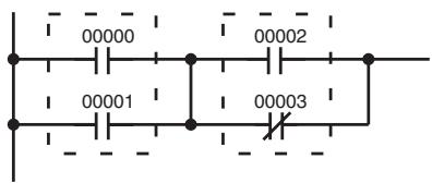
OR LOAD - OR LD
Ladder Symbol
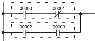
Description
When instructions are combined into blocks that cannot be logically combined using only OR and AND operations, AND LD and OR LD are used. Whereas AND and OR operations logically combine a bit status and an execution condition, AND LD and OR LD logically combine two execution conditions, the current one and the last unused one.
In order to draw ladder diagrams, it is not necessary to use AND LD and OR LD instructions, nor are they necessary when inputting ladder diagrams directly, as is possible from the CX-Programmer. They are required, however, to convert the program to and input it in mnemonic form.
In order to reduce the number of programming instructions required, a basic understanding of logic block instructions is required. For an introduction to logic blocks, refer to 4-3-6 Logic Block Instructions.
Flags
There are no flags affected by these instructions.
5-9 Bit Control Instructions
There are seven instructions that can be used generally to control individual bit status. These are OUT, OUT NOT, DIFU(13), DIFD(14), SET, RSET, and KEEP(11). These instructions are used to turn bits ON and OFF in different ways.
5-9-1 OUTPUT and OUTPUT NOT – OUT and OUT NOT
OUTPUT OUT
Ladder Symbol
Operand Data Areas

| B: Bit |
| IR, SR, AR, HR, LR, TR |
OUTPUT NOT OUT NOT
Ladder Symbol
Operand Data Areas
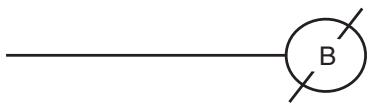
natural_image
Simple line diagram with a circle labeled 'B' and two diagonal lines (no text or symbols beyond the label)| B: Bit |
| IR, SR, AR, HR, LR |
Limitations
Any output bit can generally be used in only one instruction that controls its status.
Description
OUT and OUT NOT are used to control the status of the designated bit according to the execution condition.
OUT turns ON the designated bit for an ON execution condition, and turns OFF the designated bit for an OFF execution condition. With a TR bit, OUT appears at a branching point rather than at the end of an instruction line. Refer to 4-3-8 Branching Instruction Lines for details.
OUT NOT turns ON the designated bit for a OFF execution condition, and turns OFF the designated bit for an ON execution condition.
OUT and OUT NOT can be used to control execution by turning ON and OFF bits that are assigned to conditions on the ladder diagram, thus determining execution conditions for other instructions. This is particularly helpful and allows a complex set of conditions to be used to control the status of a single work bit, and then that work bit can be used to control other instructions.
The length of time that a bit is ON or OFF can be controlled by combining the OUT or OUT NOT with TIM. Refer to Examples under 5-16-1 TIMER – TIM for details.
Flags
There are no flags affected by these instructions.
5-9-2 SET and RESET – SET and RSET
Ladder Symbols
SET B
Operand Data Areas
B: Bit
IR, SR, AR, HR, LR
RSET B
B: Bit
IR, SR, AR, HR, LR
Description
SET turns the operand bit ON when the execution condition is ON, and does not affect the status of the operand bit when the execution condition is OFF. RSET turns the operand bit OFF when the execution condition is ON, and does not affect the status of the operand bit when the execution condition is OFF.
The operation of SET differs from that of OUT because the OUT instruction turns the operand bit OFF when its execution condition is OFF. Likewise, RSET differs from OUT NOT because OUT NOT turns the operand bit ON when its execution condition is OFF.
Precautions
The status of operand bits for SET and RSET programmed between IL(02) and ILC(03), or JMP(04) and JME(05), will not change when the interlock or jump condition is met (i.e., when IL(02) or JMP(04) is executed with an OFF execution condition).
Flags
There are no flags affected by these instructions.
Examples
The following examples demonstrate the difference between OUT and SET/RSET. In the first example (Diagram A), IR 10000 will be turned ON or OFF whenever IR 00000 goes ON or OFF.
In the second example (Diagram B), IR 10000 will be turned ON when IR 00001 goes ON and will remain ON (even if IR 00001 goes OFF) until IR 00002 goes ON.

| Address | Instruction | Operands |
| 00000 | LD | 00000 |
| 00001 | OUT | 10000 |
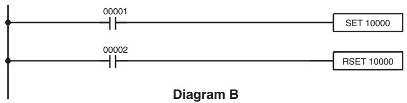
| Address | Instruction | Operands |
| 00000 | LD | 00001 |
| 00001 | SET | 10000 |
| 00002 | LD | 00002 |
| 00003 | RSET | 10000 |
5-9-3 KEEP - KEEP(11)
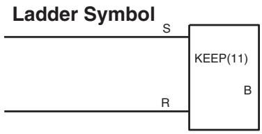
flowchart
graph LR
    S --> KEEP["KEEP(11)"]
    R --> KEEP
    KEEP --> B
    style KEEP fill:#f9f,stroke:#333
    style B fill:#ccf,stroke:#333
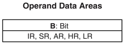
Limitations
Any output bit can generally be used in only one instruction that controls its status.
Description
KEEP(11) is used to maintain the status of the designated bit based on two execution conditions. These execution conditions are labeled S and R. S is the set input; R, the reset input. KEEP(11) operates like a latching relay that is set by S and reset by R.
When S turns ON, the designated bit will go ON and stay ON until reset, regardless of whether S stays ON or goes OFF. When R turns ON, the designated bit will go OFF and stay OFF until reset, regardless of whether R stays ON or goes OFF. The relationship between execution conditions and KEEP(11) bit status is shown below.
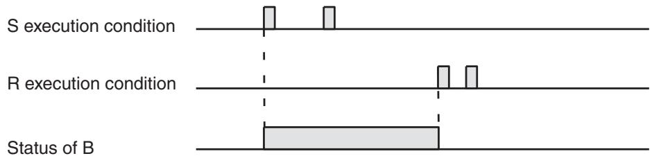
Flags
There are no flags affected by this instruction.
Precautions
Exercise caution when using a KEEP reset line that is controlled by an external normally closed device. Never use an input bit in an inverse condition on the reset (R) for KEEP(11) when the input device uses an AC power supply. The delay in shutting down the PC's DC power supply (relative to the AC power supply to the input device) can cause the designated bit of KEEP(11) to be reset. This situation is shown below.
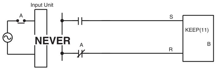
Bits used in KEEP are not reset in interlocks. Refer to the 5-12 INTERLOCK and INTERLOCK CLEAR - IL(02) and ILC(03) for details.
5-9-4 DIFFERENTIATE UP and DOWN – DIFU(13) and DIFD(14)
Ladder Symbols
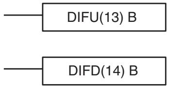
flowchart
graph TD
    A["DIFU(13) B"] --> B
    C["DIFD(14) B"] --> B
Operand Data Areas
flowchart
graph TD
    A["B: Bit"] --> B["IR, SR, AR, HR, LR"]
    C["B: Bit"] --> D["IR, SR, AR, HR, LR"]
Limitations
Any output bit can generally be used in only one instruction that controls its status.
Description
DIFU(13) and DIFD(14) are used to turn the designated bit ON for one cycle only.
Whenever executed, DIFU(13) compares its current execution with the previous execution condition. If the previous execution condition was OFF and the current one is ON, DIFU(13) will turn ON the designated bit. If the previous execution condition was ON and the current execution condition is either ON or OFF, DIFU(13) will either turn the designated bit OFF or leave it OFF (i.e., if the designated bit is already OFF). The designated bit will thus never be ON for longer than one cycle, assuming it is executed each cycle (see Precautions, below).
Whenever executed, DIFD(14) compares its current execution with the previous execution condition. If the previous execution condition was ON and the current one is OFF, DIFD(14) will turn ON the designated bit. If the previous execution condition was OFF and the current execution condition is either ON or OFF, DIFD(14) will either turn the designated bit OFF or leave it OFF. The designated bit will thus never be ON for longer than one cycle, assuming it is executed each cycle (see Precautions, below).
These instructions are used when differentiated instructions (i.e., those prefixed with an @) are not available and single-cycle execution of a particular instruction is desired. They can also be used with non-differentiated forms of instructions that have differentiated forms when their use will simplify programming. Examples of these are shown below.
Flags
There are no flags affected by these instructions.
Precautions
DIFU(13) and DIFD(14) operation can be uncertain when the instructions are programmed between IL and ILC, between JMP and JME, or in subroutines. Refer to 5-12 INTERLOCK and INTERLOCK CLEAR – IL(02) and ILC(03), 5-13 JUMP and JUMP END – JMP(04) and JME(05), 5-27 Subroutine Instructions, and 5-28-8 INTERRUPT CONTROL – INT(89).
Example
In this example, IR 10014 will be turned ON for one cycle when IR 00000 goes from OFF to ON. IR 10015 will be turned ON for one cycle when IR 00000 goes from ON to OFF.
| Address | Instruction | Operands |
| 00000 | LD | 00000 |
| 00001 | DIFU(13) | 10014 |
| 00002 | DIFD(14) | 10015 |
NOP(00) is not generally required in programming and there is no ladder symbol for it. When NOP(00) is found in a program, nothing is executed and the program execution moves to the next instruction. When memory is cleared prior to programming, NOP(00) is written at all addresses. NOP(00) can be input through the 00 function code.
Flags
There are no flags affected by NOP(00).
5-11 END - END(01)
Ladder Symbol
END(01)
Description
END(01) is required as the last instruction in any program. If there are subroutines, END(01) is placed after the last subroutine. No instruction written after END(01) will be executed. END(01) can be placed anywhere in the program to execute all instructions up to that point, as is sometimes done to debug a program, but it must be removed to execute the remainder of the program.
If there is no END(01) in the program, no instructions will be executed and the error message “NO END INST” will appear.
Flags
END(01) turns OFF the ER, CY, GR, EQ, LE, OF, and UF Flags.
5-12 INTERLOCK and INTERLOCK CLEAR – IL(02) and ILC(03)
Ladder Symbol
IL(02)
Ladder Symbol
ILC(03)
Description
IL(02) is always used in conjunction with ILC(03) to create interlocks. Interlocks are used to enable branching in the same way as can be achieved with TR bits, but treatment of instructions between IL(02) and ILC(03) differs from that with TR bits when the execution condition for IL(02) is OFF. If the execution condition of IL(02) is ON, the program will be executed as written, with an ON execution condition used to start each instruction line from the point where IL(02) is located through the next ILC(03). Refer to 4-3-8 Branching Instruction Lines for basic descriptions of both methods.
If the execution condition for IL(02) is OFF, the interlocked section between IL(02) and ILC(03) will be treated as shown in the following table:
| Instruction | Treatment |
| OUT and OUT NOT | Designated bit turned OFF. |
| TIM and TIMH(15) | Reset. |
| CNT, CNTR(12) | PV maintained. |
| KEEP(11) | Bit status maintained. |
| DIFU(13) and DIFD(14) | Not executed (see below). |
| All other instructions | The instructions are not executed, and all IR, AR, LR, HR, and SR bits and words written to as operands in the instructions are turned OFF. |
IL(02) and ILC(03) do not necessarily have to be used in pairs. IL(02) can be used several times in a row, with each IL(02) creating an interlocked section through the next ILC(03). ILC(03) cannot be used unless there is at least one IL(02) between it and any previous ILC(03).
DIFU(13) and DIFD(14) in Interlocks
Changes in the execution condition for a DIFU(13) or DIFD(14) are not recorded if the DIFU(13) or DIFD(14) is in an interlocked section and the execution condition for the IL(02) is OFF. When DIFU(13) or DIFD(14) is execution in an interlocked section immediately after the execution condition for the IL(02) has gone ON, the execution condition for the DIFU(13) or DIFD(14) will be compared to the execution condition that existed before the interlock became effective (i.e., before the interlock condition for IL(02) went OFF). The ladder diagram and bit status changes for this are shown below. The interlock is in effect while 00000 is OFF. Notice that 01000 is not turned ON at the point labeled A even though 00001 has turned OFF and then back ON.
flowchart
graph TD
    A["00000"] --> B["IL(02)"]
    C["00001"] --> D["DIFU(13) 01000"]
    E["..."] --> F["ILC(03)"]
| Address | Instruction | Operands |
| 00000 | LD | 00000 |
| 00001 | IL(02) | |
| 00002 | LD | 00001 |
| 00003 | DIFU(13) | 01000 |
| 00004 | ILC(03) |
bar
| Time | ON | OFF | |------|----|-----| | 00000 | | | | 00001 | | | | 01000 | | |Precautions
There must be an ILC(03) following any one or more IL(02).
Although as many IL(02) instructions as are necessary can be used with one ILC(03), ILC(03) instructions cannot be used consecutively without at least one IL(02) in between, i.e., nesting is not possible. Whenever a ILC(03) is executed, all interlocks between the active ILC(03) and the preceding ILC(03) are cleared.
When more than one IL(02) is used with a single ILC(03), an error message will appear when the program check is performed, but execution will proceed normally.
Flags
There are no flags affected by these instructions.
Example
The following diagram shows IL(02) being used twice with one ILC(03).
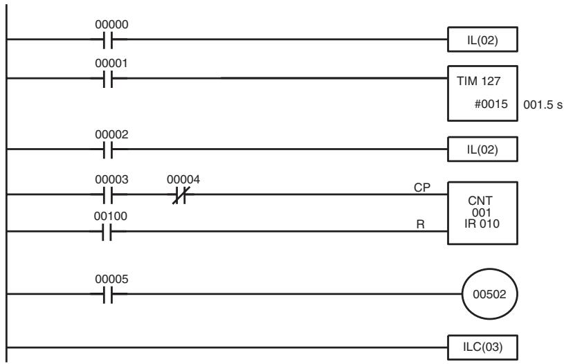
flowchart
graph TD
    A["00000"] --> B["IL(02)"]
    C["00001"] --> D["TIM 127 #0015 001.5 s"]
    E["00002"] --> F["IL(02)"]
    G["00003"] --> H["CP"]
    I["00004"] --> J["CNT 001 IR 010"]
    K["00100"] --> L["R"]
    M["00005"] --> N["00502"]
    O["ILC(03)"] --> P["00502"]
| Address | Instruction | Operands |
| 00000 | LD | 00000 |
| 00001 | IL(02) | |
| 00002 | LD | 00001 |
| 00003 | TIM | 127 |
| # 0015 | ||
| 00004 | LD | 00002 |
| 00005 | IL(02) | |
| 00006 | LD | 00003 |
| 00007 | AND NOT | 00004 |
| 00008 | LD | 00100 |
| 00009 | LD | 00100 |
| 00010 | CNT | 001 |
| 010 | ||
| 00011 | LD | 00005 |
| 00012 | OUT | 00502 |
| 00013 | ILC(03) |
When the execution condition for the first IL(02) is OFF, TIM 127 will be reset to 1.5 s, CNT 001 will not be changed, and 00502 will be turned OFF. When the execution condition for the first IL(02) is ON and the execution condition for the second IL(02) is OFF, TIM 127 will be executed according to the status of 00001, CNT 001 will not be changed, and 00502 will be turned OFF. When the execution conditions for both the IL(02) are ON, the program will execute as written.
Jump numbers 01 through 99 may be used only once in JMP(04) and once in JME(05), i.e., each can be used to define one jump only. Jump number 00 can be used as many times as desired.
Jump numbers run from 00 through 99.
Description
JMP(04) is always used in conjunction with JME(05) to create jumps, i.e., to skip from one point in a ladder diagram to another point. JMP(04) defines the point from which the jump will be made; JME(05) defines the destination of the jump. When the execution condition for JMP(04) is ON, no jump is made and the program is executed consecutively as written. When the execution condition for JMP(04) is OFF, a jump is made to the JME(05) with the same jump number and the instruction following JME(05) is executed next.
If the jump number for JMP(04) is between 01 and 99, jumps, when made, will go immediately to JME(05) with the same jump number without executing any instructions in between. The status of timers, counters, bits used in OUT, bits used in OUT NOT, and all other status bits controlled by the instructions between JMP(04) and JMP(05) will not be changed. Each of these jump num-
| bers can be used to define only one jump. Because all of instructions between JMP(04) and JME(05) are skipped, jump numbers 01 through 99 can be used to reduce cycle time.Jump Number 00If the jump number for JMP(04) is 00, the CPU Unit will look for the next JME(05) with a jump number of 00. To do so, it must search through the program, causing a longer cycle time (when the execution condition is OFF) than for other jumps.The status of timers, counters, bits used in OUT, bits used in OUT NOT, and all other status controlled by the instructions between JMP(04) 00 and JMP(05) 00 will not be changed. Jump number 00 can be used as many times as desired. A jump from JMP(04) 00 will always go to the next JME(05) 00 in the program. It is thus possible to use JMP(04) 00 consecutively and match them all with the same JME(05) 00. It makes no sense, however, to use JME(05) 00 consecutively, because all jumps made to them will end at the first JME(05) 00. | |
| DIFU(13) and DIFD(14) in Jumps | Although DIFU(13) and DIFD(14) are designed to turn ON the designated bit for one cycle, they will not necessarily do so when written between JMP(04) and JMP (05). Once either DIFU(13) or DIFD(14) has turned ON a bit, it will remain ON until the next time DIFU(13) or DIFD(14) is executed again. In normal programming, this means the next cycle. In a jump, this means the next time the jump from JMP(04) to JME(05) is not made, i.e., if a bit is turned ON by DIFU(13) or DIFD(14) and then a jump is made in the next cycle so that DIFU(13) or DIFD(14) are skipped, the designated bit will remain ON until the next time the execution condition for the JMP(04) controlling the jump is ON. |
| Precautions | When JMP(04) and JME(05) are not used in pairs, an error message will appear when the program check is performed. This message also appears if JMP(04) 00 and JME(05) 00 are not used in pairs, but the program will execute properly as written. |
| Flags | There are no flags affected by these instructions. |
| Examples | Examples of jump programs are provided in 4-3-9 Jumps. |
5-14 User Error Instructions: FAILURE ALARM AND RESET – FAL(06) and SEVERE FAILURE ALARM – FALS(07)
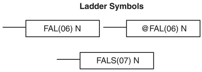
flowchart
graph TD
    A["FAL(06) N"] --> B["@FAL(06) N"]
    C["FALS(07) N"] --> D
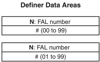
Description
FAL(06) and FALS(07) are provided so that the programmer can output error numbers for use in operation, maintenance, and debugging. When executed with an ON execution condition, either of these instructions will output a FAL number to bits 00 to 07 of SR 253. The FAL number that is output can be between 01 and 99 and is input as the definer for FAL(06) or FALS(07). FAL(06) with a definer of 00 is used to reset this area (see below).
FAL Area
FAL(06) produces a non-fatal error and FALS(07) produces a fatal error. When FAL(06) is executed with an ON execution condition, the ALARM/ERROR indicator on the front of the CPU Unit will flash, but PC operation will continue. When FALS(07) is executed with an ON execution condition, the ALARM/ERROR indicator will light and PC operation will stop.
The system also generates error codes to the FAL area.
Resetting Errors
FAL error codes will be retained in memory, although only one of these is available in the FAL area. To access the other FAL codes, reset the FAL area by executing FAL(06) 00. Each time FAL(06) 00 is executed, another FAL error will be moved to the FAL area, clearing the one that is already there. FAL error codes are recorded in numerical order.
FAL(06) 00 is also used to clear message programmed with the instruction, MSG(46).
If the FAL area cannot be cleared, as is generally the case when FALS(07) is executed, first remove the cause of the error and then clear the FAL area through the Programming Console or the CX-Programmer.
5-15 Step Instructions: STEP DEFINE and STEP START–STEP(08)/SNXT(09)
Ladder Symbols
STEP(08) B
STEP(08)
Definer Data Areas
B: Control bit
IR, AR, HR, LR
SNXT(09) B
B: Control bit
IR, AR, HR, LR
Limitations
All control bits must be in the same word and must be consecutive.
Description
The step instructions STEP(08) and SNXT(09) are used together to set up breakpoints between sections in a large program so that the sections can be executed as units and reset upon completion. A section of program will usually be defined to correspond to an actual process in the application. (Refer to the application examples later in this section.) A step is like a normal programming code, except that certain instructions (i.e., END(01), IL(02)/ILC(03), JMP(04)/JME(05), and SBN(92)) may not be included.
STEP(08) uses a control bit in the IR or HR areas to define the beginning of a section of the program called a step. STEP(08) does not require an execution condition, i.e., its execution is controlled through the control bit. To start execution of the step, SNXT(09) is used with the same control bit as used for STEP(08). If SNXT(09) is executed with an ON execution condition, the step with the same control bit is executed. If the execution condition is OFF, the step is not executed. The SNXT(09) instruction must be written into the program so that it is executed before the program reaches the step it starts. It can
be used at different locations before the step to control the step according to two different execution conditions (see example 2, below). Any step in the program that has not been started with SNXT(09) will not be executed.
Once SNXT(09) is used in the program, step execution will continue until STEP(08) is executed without a control bit. STEP(08) without a control bit must be preceded by SNXT(09) with a dummy control bit. The dummy control bit may be any unused IR or HR bit. It cannot be a control bit used in a STEP(08).
Execution of a step is completed either by execution of the next SNXT(09) or by turning OFF the control bit for the step (see example 3 below). When the step is completed, all of the IR and HR bits in the step are turned OFF and all timers in the step are reset to their SVs. Counters, shift registers, and bits used in KEEP(11) maintain status. Two simple steps are shown below.
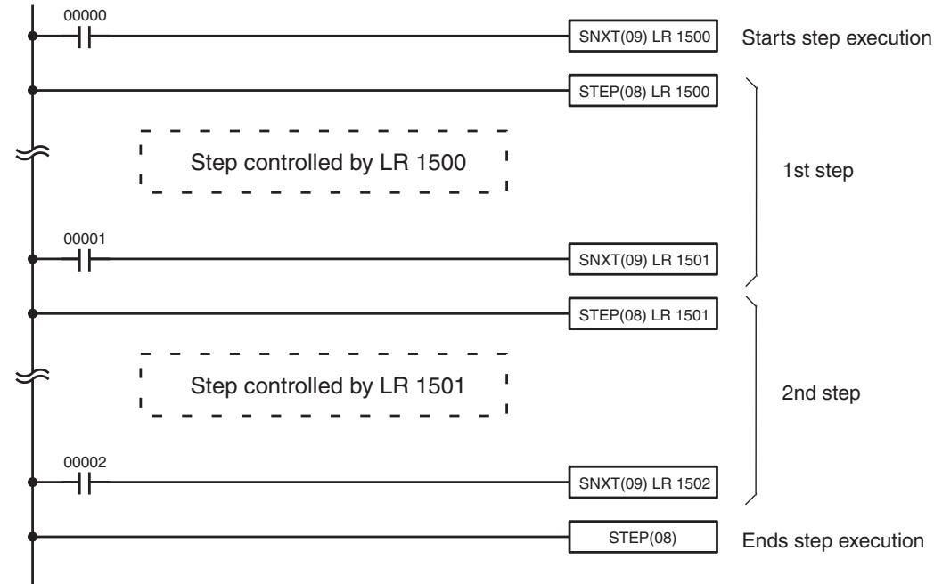
flowchart
graph TD
    A["Start"] --> B["SNXT(09) LR 1500"]
    B --> C["STEP(08) LR 1500"]
    C --> D["Step controlled by LR 1500"]
    D --> E["SNXT(09) LR 1501"]
    E --> F["STEP(08) LR 1501"]
    F --> G["Step controlled by LR 1501"]
    G --> H["SNXT(09) LR 1502"]
    H --> I["STEP(08)"]
    I --> J["Ends step execution"]
| Address | Instruction | Operands |
| 00000 | LD | 00000 |
| 00001 | SNXT(09) | LR 1500 |
| 00002 | STEP(08) | LR 1500 |
| Step controlled by LR 1500. | ||
| 00100 | LD | 00001 |
| 00101 | SNXT(09) | LR 1501 |
| Address | Instruction | Operands |
| 00102 | STEP(08) | LR 1501 |
| Step controlled by LR 1501. | ||
| 00200 | LD | 00002 |
| 00201 | SNXT(09) | LR 1502 |
| 00202 | STEP(08) | --- |
Steps can be programmed in consecutively. Each step must start with STEP(08) and generally ends with SNXT(09) (see example 3, below, for an exception). When steps are programmed in series, three types of execution are possible: sequential, branching, or parallel. The execution conditions for, and the positioning of, SNXT(09) determine how the steps are executed. The three examples given below demonstrate these three types of step execution.
Precautions
Interlocks, jumps, SBN(92), and END(01) cannot be used within step programs.
Bits used as control bits must not be used anywhere else in the program unless they are being used to control the operation of the step (see example 3, below). All control bits must be in the same word and must be consecutive.
If IR or LR bits are used for control bits, their status will be lost during any power interruption. If it is necessary to maintain status to resume execution at the same step, HR bits must be used.
Flags
25407: Step Start Flag; turns ON for one cycle when STEP(08) is executed and can be used to reset counters in steps as shown below if necessary.
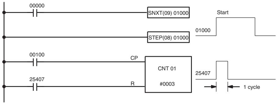
flowchart
graph LR
    A["00000"] --> B["SNXT(09) 01000"]
    B --> C["01000"]
    D["00100"] --> E["CP"]
    E --> F["CNT 01"]
    G["25407"] --> H["R"]
    H --> I["#0003"]
    J["Start"] --> K["25407"]
    L["1 cycle"] --> M["End"]
| Address | Instruction | Operands |
| 00000 | LD | 00000 |
| 00001 | SNXT(09) | 01000 |
| 00002 | STEP(08) | 01000 |
| 00003 | LD | 00100 |
| Address | Instruction | Operands |
| 00004 | LD | 25407 |
| 00005 | CNT | 01 |
| # 0003 |
5-16 Timer and Counter Instructions
TIM and TIMH(15) are decrementing ON-delay timer instructions which require a TIM/CNT number and a set value (SV). STIM(69) is used to control the interval timers, which are used to activate interrupt routines.
CNT is a decrementing counter instruction and CNTR(12) is a reversible counter instruction. Both require a TIM/CNT number and a SV. Both are also connected to multiple instruction lines which serve as an input signal(s) and a reset. CTBL(63), INT(89), and PRV(62) are used to manage the high-speed counter. INT(89) is also used to stop pulse output.
Any one TIM/CNT number cannot be defined twice, i.e., once it has been used as the definer in any of the timer or counter instructions, it cannot be used again. Once defined, TIM/CNT numbers can be used as many times as required as operands in instructions other than timer and counter instructions.
TIM/CNT numbers run from 000 through 511. No prefix is required when using a TIM/CNT number as a definer in a timer or counter instruction. Once defined as a timer, a TIM/CNT number can be prefixed with TIM for use as an operand in certain instructions. The TIM prefix is used regardless of the timer instruction that was used to define the timer. Once defined as a counter, a TIM/CNT number can be prefixed with CNT for use as an operand in certain instructions. The CNT is also used regardless of the counter instruction that was used to define the counter.
TIM/CNT numbers can be designated as operands that require either bit or word data. When designated as an operand that requires bit data, the TIM/CNT number accesses a bit that functions as a `Completion Flag' that indicates when the time/count has expired, i.e., the bit, which is normally OFF, will turn ON when the designated SV has expired. When designated as an operand that requires word data, the TIM/CNT number accesses a memory location that holds the present value (PV) of the timer or counter. The PV of a timer or counter can thus be used as an operand in CMP(20), or any other
instruction for which the TIM/CNT area is allowed. This is done by designating the TIM/CNT number used to define that timer or counter to access the memory location that holds the PV.
Note that “TIM 000” is used to designate the TIMER instruction defined with TIM/CNT number 000, to designate the Completion Flag for this timer, and to designate the PV of this timer. The meaning of the term in context should be clear, i.e., the first is always an instruction, the second is always a bit operand, and the third is always a word operand. The same is true of all other TIM/CNT numbers prefixed with TIM or CNT.
An SV can be input as a constant or as a word address in a data area. If an IR area word assigned to an Input Unit is designated as the word address, the Input Unit can be wired so that the SV can be set externally through thumb-wheel switches or similar devices. Timers and counters wired in this way can only be set externally during RUN or MONITOR mode. All SVs, including those set externally, must be in BCD.
5-16-1 TIMER - TIM
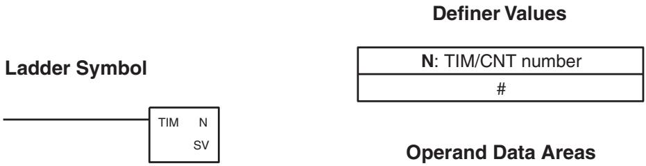
| SV: Set value (word, BCD) |
| IR, SR, AR, DM, EM, HR, LR, # |
Limitations
SV is between 000.0 and 999.9. The decimal point is not entered.
The EM area is available in CQM1H-CPU61 CPU Units only.
Each TIM/CNT number can be used as the definer in only one TIMER or COUNTER instruction.
TIM/CNT 000 through TIM/CNT 015 should not be used in TIM if they are required for TIMH(15). Refer to 5-16-4 HIGH-SPEED TIMER – TIMH(15) for details.
Description
A timer is activated when its execution condition goes ON and is reset (to SV) when the execution condition goes OFF. Once activated, TIM measures in units of 0.1 second from the SV.
If the execution condition remains ON long enough for TIM to time down to zero, the Completion Flag for the TIM/CNT number used will turn ON and will remain ON until TIM is reset (i.e., until its execution condition is goes OFF).
The following figure illustrates the relationship between the execution condition for TIM and the Completion Flag assigned to it.
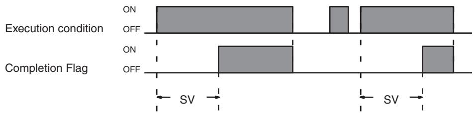
other
| State | Event Type | Duration | |-----------|------------------|----------| | ON | ON | 100 | | ON | OFF | 100 | | ON | ON | 100 | | ON | OFF | 100 | | Completion Flag | ON | 100 | | Completion Flag | OFF | 100 |Precautions
Timers in interlocked program sections are reset when the execution condition for IL(02) is OFF. Power interruptions also reset timers. If a timer that is not reset under these conditions is desired, SR area clock pulse bits can be counted to produce timers using CNT. Refer to 5-16-2 COUNTER – CNT for details.
Note The timer set value must be BCD between #0000 and #9999. Operation will be as follows if #0000 or #0001 is set.
- If #0000 is set, the Completion Flag will turn ON as soon as the timer's execution condition turns ON.
- If #0001 is set, the Completion Flag may turn ON as soon as the timer's execution condition turns ON because timer accuracy is 0 to -0.1 s.
Consider the timer accuracy (0 to -0.1 s) when determining the proper set value.
Flags
ER: SV is not in BCD.
Indirectly addressed EM/DM word is non-existent.
(Content of *EM/*DM word is not BCD, or the EM/DM area boundary has been exceeded.)
5-16-2 COUNTER - CNT
Definer Values
Ladder Symbol
| CP | CNT N |
| R | SV |
| N: TIM/CNT number |
| # |
Operand Data Areas
| SV: Set value (word, BCD) |
| IR, SR, AR, DM, EM, HR, LR, # |
Limitations
Each TIM/CNT number can be used as the definer in only one TIMER or COUNTER instruction.
The EM area is available in CQM1H-CPU61 CPU Units only.
Description
CNT is used to count down from SV when the execution condition on the count pulse, CP, goes from OFF to ON, i.e., the present value (PV) will be decremented by one whenever CNT is executed with an ON execution condition for CP and the execution condition was OFF for the last execution. If the execution condition has not changed or has changed from ON to OFF, the PV of CNT will not be changed. The Completion Flag for a counter is turned ON when the PV reaches zero and will remain ON until the counter is reset.
CNT is reset with a reset input, R. When R goes from OFF to ON, the PV is reset to SV. The PV will not be decremented while R is ON. Counting down from SV will begin again when R goes OFF. The PV for CNT will not be reset in interlocked program sections or by power interruptions.
Changes in execution conditions, the Completion Flag, and the PV are illustrated below. PV line height is meant only to indicate changes in the PV.
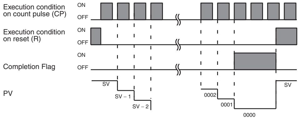
flowchart
graph TD
    A["Execution condition on count pulse (CP)"] --> B["ON"]
    A --> C["OFF"]
    D["Execution condition on reset (R)"] --> E["ON"]
    D --> F["OFF"]
    G["Completion Flag"] --> H["ON"]
    G --> I["OFF"]
    J["PV"] --> K["SV - 1"]
    J --> L["SV - 2"]
    M["0002"] --> N["0001"]
    O["0000"] --> P["0000"]
Precautions
Program execution will continue even if a non-BCD SV is used, but the SV will not be correct.
Flags
ER: SV is not in BCD.
Indirectly addressed EM/DM word is non-existent.
(Content of *EM/*DM word is not BCD, or the EM/DM area boundary has been exceeded.)
Example
In the following example, CNT is used to create extended timers by counting SR area clock pulse bits.
CNT 001 counts the number of times the 1-second clock pulse bit (SR 25502) goes from OFF to ON. Here again, IR 00000 is used to control the times when CNT is operating.
Because in this example the SV for CNT 001 is 700, the Completion Flag for CNT 002 turns ON when 1 second x 700 times, or 11 minutes and 40 seconds have expired. This would result in IR 01602 being turned ON.
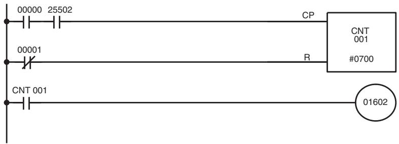
| Address | Instruction | Operands |
| 00000 | LD | 00000 |
| 00001 | AND | 25502 |
| 00002 | LD NOT | 00001 |
| 00003 | CNT | 001 |
| # 0700 | ||
| 00004 | LD | CNT 001 |
| 00005 | OUT | 01602 |

The shorter clock pulses will not necessarily produce accurate timers because their short ON times might not be read accurately during longer cycles. In particular, the 0.02-second and 0.1-second clock pulses should not be used to create timers with CNT instructions.
5-16-3 REVERSIBLE COUNTER - CNTR(12)
Ladder Symbol
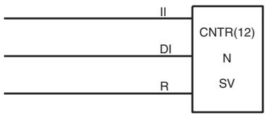
Definer Values
| N: TIM/CNT number |
| # |
Operand Data Areas
| SV: Set value (word, BCD) |
| IR, SR, AR, DM, EM, HR, LR, # |
Limitations
Each TIM/CNT number can be used as the definer in only one TIMER or COUNTER instruction.
The EM area is available in CQM1H-CPU61 CPU Units only.
Description
The CNTR(12) is a reversible, up/down circular counter, i.e., it is used to count between zero and SV according to changes in two execution conditions, those in the increment input (II) and those in the decrement input (DI).
The present value (PV) will be incremented by one whenever CNTR(12) is executed with an ON execution condition for II and the last execution condition for II was OFF. The present value (PV) will be decremented by one whenever CNTR(12) is executed with an ON execution condition for DI and the last execution condition for DI was OFF. If OFF to ON changes have occurred in both II and DI since the last execution, the PV will not be changed.
If the execution conditions have not changed or have changed from ON to OFF for both II and DI, the PV of CNT will not be changed.
When decremented from 0000, the present value is set to SV and the Completion Flag is turned ON until the PV is decremented again. When incremented past the SV, the PV is set to 0000 and the Completion Flag is turned ON until the PV is incremented again.
CNTR(12) is reset with a reset input, R. When R goes from OFF to ON, the PV is reset to zero. The PV will not be incremented or decremented while R is ON. Counting will begin again when R goes OFF. The PV for CNTR(12) will not be reset in interlocked program sections or by the effects of power interruptions.
Changes in II and DI execution conditions, the Completion Flag, and the PV are illustrated below starting from part way through CNTR(12) operation (i.e., when reset, counting begins from zero). PV line height is meant to indicate changes in the PV only.
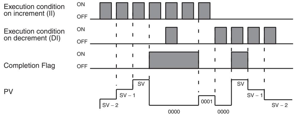
other
| State | Condition | Value | |-------|-----------|-------| | ON | ON increment (II) | ON | | ON | ON decrement (DI) | ON | | ON | ON Completion Flag | ON | | ON | OFF Completion Flag | OFF | | SV-1 | SV-1 | SV-1 | | SV-2 | SV-2 | SV-2 | | 0000 | 0001 | 0001 | | 0000 | SV | SV | | 0000 | SV-1 | SV-1 | | 0000 | SV-2 | SV-2 |Precautions
Program execution will continue even if a non-BCD SV is used, but the SV will not be correct.
Flags
ER: SV is not in BCD.
Indirectly addressed EM/DM word is non-existent.
(Content of *EM/*DM word is not BCD, or the EM/DM area boundary has been exceeded.)
| SV: Set value (word, BCD) |
| IR, SR, AR, DM, EM, HR, LR, # |
Limitations
SV is between 00.00 and 99.99. (Although 00.00 and 00.01 may be set, 00.00 will disable the timer, i.e., turn ON the Completion Flag immediately, and 00.01 is not reliably scanned.) The decimal point is not entered.
The EM area is available in CQM1H-CPU61 CPU Units only.
Each TIM/CNT number can be used as the definer in only one TIMER or COUNTER instruction. Use TIM/CNT numbers from 000 through 015. High-speed timers with timer numbers TIM/CNT 016 through TIM/CNT 511 should not be used if the cycle time exceeds 10 ms.
Description
TIMH(15) operates in the same way as TIM except that TIMH measures in units of 0.01 second. Refer to 5-16-1 TIMER - TIM for operational details.
Precautions
Timers in interlocked program sections are reset when the execution condition for IL(02) is OFF. Power interruptions also reset timers. If a timer that is not reset under these conditions is desired, SR area clock pulse bits can be counted to produce timers using CNT. Refer to 5-16-2 COUNTER – CNT for details.
Timers in jumped program sections will not be reset when the execution condition for JMP(04) is OFF, but the timer will stop timing if jump number 00 is used. The timers will continue timing if jump numbers 01 through 99) are used.
High-speed timers with timer numbers TIM/CNT 000 through TIM/CNT 015 will not be inaccurate when the PC Setup (DM 6629) is set to perform interrupt processing on these timers.
High-speed timers with timer numbers TIM/CNT 016 through TIM/CNT 511 will be inaccurate when the cycle time exceeds 10 ms. If the cycle time is greater than 10 ms, use TIM/CNT 000 through TIM/CNT 015 and set DM 6629 for interrupt processing of the timer numbers used.
Note The timer set value must be BCD between #0000 and #9999. Operation will be as follows if #0000 or #0001 is set.
- If #0000 is set, the Completion Flag will turn ON as soon as the timer's execution condition turns ON (but there may be a delay if TIM 000 to TIM 015 are used).
- If #0001 is set, the Completion Flag may turn ON as soon as the timer's execution condition turns ON because timer accuracy is 0 to -0.01 s.
Consider the timer accuracy (0 to -0.01 s) when determining the proper set value.
Flags
ER: SV is not in BCD.
Indirectly addressed EM/DM word is non-existent.
(Content of *EM/*DM word is not BCD, or the EM/DM area boundary has been exceeded.)
Example
The following example shows a timer set with a constant. 01600 will be turned ON after 00000 goes ON and stays ON for at least 1.5 seconds. When 00000 goes OFF, the timer will be reset and 01600 will be turned OFF.
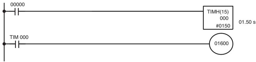
| Address | Instruction | Operands |
| 00000 | LD | 00000 |
| 00001 | TIMH(15) | 000 |
| # 0150 | ||
| 00002 | LD | TIM 000 |
| 00003 | OUT | 01600 |
5-16-5 TOTALIZING TIMER - TTIM(—)
Ladder Symbol
| TTIM(—) |
| N |
| SV |
| RB |
Definer Values
| N: TIM/CNT number |
| # (000 through 511) |
Operand Data Areas
| SV: Set value (word, BCD) |
| IR, AR, DM, EM, HR, LR |
RB: Reset bit
IR, SR, AR, HR, LR
Limitations
SV is between 0000 and 9999 and must be in BCD. The decimal point is not entered.
The EM area is available in CQM1H-CPU61 CPU Units only.
Each TIM/CNT number can be used as the definer in only one TIMER or COUNTER instruction.
Description
TTIM(—) is used to create a timer that increments the PV every 0.1 s to time between 0.1 and 999.9 s. TTIM(—) increments in units of 0.1 second from zero. TTIM(—) accuracy is +0.0/-0.1 second. A TTIM(—) timer will time as long as its execute condition is ON until it reaches the SV or until RB turns ON to reset the timer. TTIM(—) timers will time only as long as they are executed every cycle, i.e., they do not time, but maintain the current PV, in interlocked program sections or when they are jumped in the program.
Note The PVs of decrementing timers such as TIM indicate the time remaining until the timer times out, but the PVs of TTIM(—) timers indicate the time that has elapsed. The TTIM(—) PV can be used “as is” to represent the elapsed time in calculations and displays.
Precautions
The PV will be reset to 0000 and the Completion Flag will be turned OFF when a power interruption occurs or the PC is switched from PROGRAM mode to MONITOR or RUN mode (or vice-versa).
The PV of TTIM(—) in an interlocked program section will be maintained when the execution condition for IL(02) is OFF. The PV will also be maintained in a jumped program section, unlike timers and high-speed timers which continue timing.
TTIM(—) will not operate properly if the cycle time exceeds 0.1 s because the PV is refreshed only when TTIM(—) is executed and the PV is incremented in 0.1-s units.
A delay of one cycle is sometimes required for a Completion Flag to be turned ON after the timer times out because the Completion Flag is refreshed only when TTIM(—) is executed.
TTIM(—) will not restart after timing out unless the PV is changed to a value below the SV or the reset input is turned ON.
Note The timer set value must be BCD between #0000 and #9999. Operation will be as follows if #0000 or #0001 is set.
- If #0000 is set, the Completion Flag will turn ON as soon as the timer's execution condition turns ON.
- If #0001 is set, the Completion Flag may turn ON as soon as the timer's execution condition turns ON because timer accuracy is 0 to -0.1 s.
Consider the timer accuracy (0 to -0.1 s) when determining the proper set value.
Flags
ER: SV is not in BCD.
Indirectly addressed EM/DM word is non-existent.
(Content of *EM/*DM word is not BCD, or the EM/DM area boundary has been exceeded.)
Flags
ER: N is not a TIM number.
SV is not BCD.
RB is not a valid bit address.
Indirectly addressed EM/DM word is non-existent.
(Content of *EM/*DM word is not BCD, or the EM/DM area boundary has been exceeded.)
Example
The following figure illustrates the relationship between the execution conditions for a totalizing timer with a set value of 2 s, its PV, and the Completion Flag.
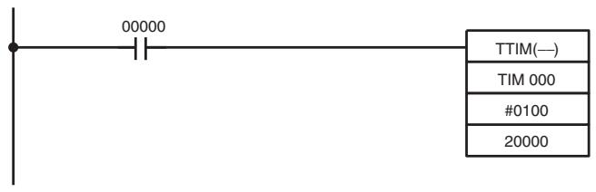
| Address | Instruction | Operands |
| 00000 | LD | 00000 |
| 00001 | TTIM(—) | |
| TIM 000 | ||
| # 0100 | ||
| 20000 |
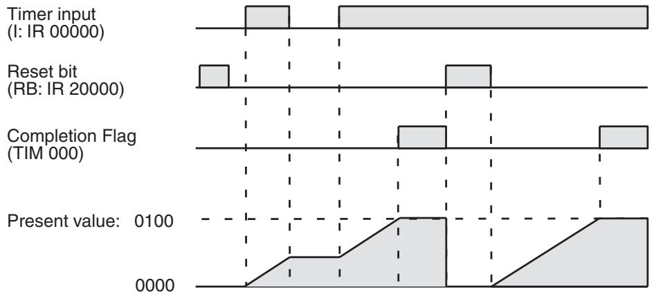
other
| Signal Type | Value | | ----------------------- | ----- | | Timer input (I: IR 00000) | 1 | | Reset bit (RB: IR 20000) | 1 | | Completion Flag (TIM 000) | 1 | | Present value: 0100 | 0100 | | Present value: 0000 | 0000 |5-16-6 INTERVAL TIMER - STIM(69)
Ladder Symbols
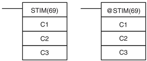
flowchart
graph TD
    A["STIM(69)"] --> B["C1"]
    A --> C["C2"]
    A --> D["C3"]
    E["@STIM(69)"] --> F["C1"]
    E --> G["C2"]
    E --> H["C3"]
Operand Data Areas
| C1: Control data #1 |
| 000 to 008, 010 to 012 |
| C2: Control data #2 |
| IR, SR, AR, DM, EM, HR, TIM/CNT, LR, # |
| C3: Control data #3 |
| IR, SR, AR, DM, EM, HR, TIM/CNT, LR, # |
Limitations
C1 must be 000 to 008 or 010 to 012.
If C1 is 000 to 005, a constant greater than 0255 cannot be used for C3. If C1 is 006 to 008, constants and DM 6143 to DM 6655 cannot be used for C2 or C3. If C1 is 010 to 012, both C2 and C3 must be set to 000.
Description
STIM(69) is used to control the interval timers by performing four basic functions: starting the timer for a non-shot interrupt, starting the timer for scheduled interrupts, stopping the timer, and reading the timer's PV. Set the value of C1 to specify which of these functions will be performed and which of the three interval timers it will be performed on, as shown in the following table. Refer to 1-4-5 Interval Timer Interrupts for more detailed descriptions of using interval timer interrupts. STIM(69) is also described in more detail after the table.
| Function | Timer | C1 value |
| Starting timers | 0 | 000 |
| 1 | 001 | |
| 2 | 002 | |
| Starting scheduled interrupts | 0 | 003 |
| 1 | 004 | |
| 2 | 005 | |
| Reading timer PV | 0 | 006 |
| 1 | 007 | |
| 2 | 008 | |
| Stopping timers | 0 | 010 |
| 1 | 011 | |
| 2 | 012 |
| Note | 1. Interval timer 0 cannot be used when a pulse output is being output by the SPED(64) instruction.2. Interval timer 2 cannot be used when high-speed counter 0 operation has been enabled in DM 6642 of the PC Setup. | |
| Starting Interrupts | Set C1=000 to 002 to start timers 0 to 2 to activate a one-shot interrupt. Set C1=003 to 005 to start scheduled interrupts using timers 0 to 2.C2, which specifies the timer's SV, can be a constant or the first of two words containing the SV. The settings are slightly different depending on the method used.If C2 is a constant, it specifies the initial value of the decrementing counter (BCD, 0000 to 9999). The decrementing time interval is 1 ms.If C2 is a word address, C2 specifies the initial value of the decrementing counter (BCD, 0000 to 9999), and C2+1 specifies the decrementing time interval (BCD, 0005 to 0320) in units of 0.1 ms. The decrementing time interval can thus be 0.5 to 32 ms.C3 specifies subroutine number 0000 to 0255. | |
| Note The time required from interval timer start-up to time-up is: (the content of C2) × (the content of C2+1) × 0.1 ms | ||
| Reading Timer PVs | Set C1=006 to 008 to read the PVs of timers 0 to 2.C2 specifies the first of two destination words that will receive the timer's PV. C2 will receive the number of times the decrementing counter has been decremented (BCD, 0000 to 9999) and C2+1 will receive the decrementing time interval (BCD in 0.1 ms units).C3 specifies the destination word that will receive the time which has elapsed since the last time the timer was decremented (BCD in 0.1 ms units). (Must be equal to or less than the decrementing time interval set in C2+1.) | |
| Note The time that has elapsed since the timer was started is computed as follows: (Content of C2 × (Content of C2 + 1) + Content of C3) × 0.1 ms | ||
| Stopping Timers | Set C1=010 to 012 to stop timers 0 to 2.C2 and C3 have no function and should both be set to 000. | |
| Flags | ER: Interval timer 0 is started while a pulse output is operating. (C1=000 only)Interval timer 2 is started while the high-speed counter 0 is enabled (C1=002 only)Indirectly addressed EM/DM word is non-existent. (Content of *EM/*DM word is not BCD, or the EM/DM area boundary has been exceeded.)A data area boundary has been exceeded. | |
5-16-7 REGISTER COMPARISON TABLE – CTBL(63)
Ladder Symbols
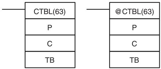
Operand Data Areas
| P: Port specifier |
| 000 to 004 or 101 to 104 |
| C: Control data |
| 000 to 003 |
| TB: First comparison table word |
| IR, SR, AR, DM, EM, HR, LR |
Limitations
The first and last comparison table words must be in the same data area. (The length of the comparison table varies according to the settings.)
CTBL(63) cannot be used if the PC Setup (DM 6611) is set to pulse output mode.
Description
CTBL(63) is used to register comparison tables and start comparison for high-speed counters. The following table shows the functions of CTBL(63).
| Unit/Board | Function |
| CPU Unit | High-speed counter 0 (IR 00004 to IR 00006) |
| Pulse I/O Board | High-speed counters 1 and 2 |
| Absolute Encoder Interface Board | Absolute high-speed counters 1 and 2 |
| High-speed Counter Board | High-speed counters 1 to 4 |
CPU Unit, Pulse I/O Board, and Absolute Encoder Interface Board
The description of CTBL(63) operation is divided into two parts. Refer to page 243 for a description of operation for the CPU Unit, Pulse I/O Board, and Absolute Encoder Interface Board. Refer to page 248 for details on CTBL(63) operation with the High-speed Counter Board.
When the execution condition is OFF, CTBL(63) is not executed. When the execution condition is ON, CTBL(63) registers a comparison table for use with the high-speed counter PV. Depending on the value of C, comparison with the high-speed counter PV can begin immediately or it can be started separately with INI(61).
The port specifier (P) specifies the high-speed counter that will be used in the comparison.
| Unit/Board | Function | Port specifier (P) |
| CPU Unit | High-speed counter 0 (built-in) | 000 |
| Pulse I/O Board(See notes 1 and 2) | High-speed counter 1 | 001 |
| High-speed counter 2 | 002 | |
| Absolute EncoderInterface Board(See note 1) | High-speed counter 1 | 001 |
| High-speed counter 2 | 002 |
Note
- The Pulse I/O Board and Absolute Encoder Interface Board must be installed in slot 2.
- When a Pulse I/O Board is being used, the mode for ports 1 and 2 must be set to high-speed counter mode in DM 6611 of the PC Setup. CTBL(63) cannot be used if the mode is set to simple positioning mode.
The function of CTBL(63) is determined by the control data, C, as shown in the following table. These functions are described after the table.
| C | CTBL(63) function |
| 000 | Registers a target value comparison table and starts comparison. |
| 001 | Registers a range comparison table and starts comparison. |
| 002 | Registers a target value comparison table. Start comparison with INI(61). |
| 003 | Registers a range comparison table. Start comparison with INI(61). |
When the PV agrees with a target value or falls within a specified range, the specified subroutine is called and executed. Refer to 1-4-6 High-speed Counter 0 Interrupts for more details on table comparison.
If the high-speed counter is enabled in the PC Setup (DM 6642), it will begin counting from zero when the CQM1H begins operation. The PV will not be compared to the comparison table until the table is registered and comparison is initiated with INI(61) or CTBL(63). Comparison can be stopped and started, or the PV can be reset with INI(61).
Once a comparison table has been registered, it is valid until the CQM1H is halted or until an error occurs in attempting to register a new table. The differentiated form of CTBL(63) is recommended when possible to reduce cycle time.
Target Value Comparison
For high-speed counter 0 in the CPU Unit, up to 16 target values can be registered. A subroutine number (1 to 16) is also registered for each target value. For high-speed counters 1 and 2 on a Pulse I/O Board or Absolute Encoder Interface Board, up to 48 target values can be registered. A subroutine number (1 to 48) is also registered for each target value. In either case, the corresponding subroutine is called and executed when the PV matches a target value. (When interrupt processing is not required, an undefined subroutine number may be entered.)
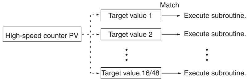
flowchart
graph TD
    A["High-speed counter PV"] --> B["Target value 1"]
    A --> C["Target value 2"]
    A --> D["..."]
    A --> E["Target value 16/48"]
    B --> F["Match"]
    C --> G["Match"]
    E --> H["Match"]
    F --> I["Execute subroutine."]
    G --> J["Execute subroutine."]
    H --> K["..."]
    I --> L["Execute subroutine."]
Target value comparisons are performed one item at a time in order of the comparison table. When the PV reaches the first target value in the table, the interrupt subroutine is executed and comparison continues to the next value in the table. When processing has been completed for the last target value in the table, comparison returns to the first value in the table and the process is repeated.
The following diagram shows the structure of a target value comparison table for use with the CPU Unit's built-in high-speed counter 0 or the Pulse I/O Board's high-speed counters 1 or 2 set for linear counting. The number of target values can be 0001 to 0048.
The following diagram shows the structure of a target value comparison table for use with the Pulse I/O Board's high-speed counters 1 or 2 set for ring counting. Input the target values in ascending or descending order.
The ring value specifies the number of points in the ring and the maximum count value (ring value = max. count value + 1). The ring value can be 0 to 65,000. Do not change the ring value while a comparison is in progress.
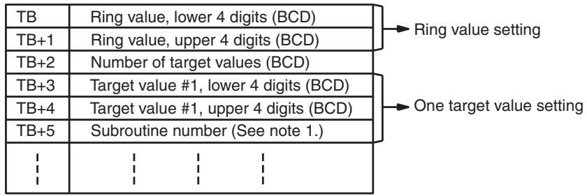
flowchart
graph TD
    A["TB"] --> B["Ring value, lower 4 digits (BCD)"]
    C["TB+1"] --> D["Ring value, upper 4 digits (BCD)"]
    E["TB+2"] --> F["Number of target values (BCD)"]
    G["TB+3"] --> H["Target value #1, lower 4 digits (BCD)"]
    I["TB+4"] --> J["Target value #1, upper 4 digits (BCD)"]
    K["TB+5"] --> L["Subroutine number (See note 1.)"]
    M[" "] --> N[" "]
    O[" "] --> P[" "]
    Q[" "] --> R[" "]
    S[" "] --> T[" "]
    U[" "] --> V[" "]
    W[" "] --> X[" "]
    Y[" "] --> Z[" "]
    AA[" "] --> AB[" "]
    AC[" "] --> AD[" "]
    AE[" "] --> AF[" "]
    AG[" "] --> AH[" "]
    AI[" "] --> AJ[" "]
    AK[" "] --> AL[" "]
    AM[" "] --> AN[" "]
    AO[" "] --> AP[" "]
    AQ[" "] --> AR[" "]
    AS[" "] --> AT[" "]
    AU[" "] --> AV[" "]
    AW[" "] --> AX[" "]
    AY[" "] --> AZ[" "]
    BA[" "] --> BB[" "]
    BC[" "] --> BC
    AD[" "] --> AD
    AE[" "] --> AE
    AF[" "] --> AF
    AG[" "] --> AG
    AH[" "] --> AH
    AI[" "] --> AI
    AJ[" "] --> AJ
    AK[" "] --> AK
    AL[" "] --> AL
    AM[" "] --> AM
    AN[" "] --> AN
    AO[" "] --> AO
    AP[" "] --> AP
    AQ[" "] --> AQ
    AR[" "] --> AR
    AS[" "] --> AS
    AT[" "] --> AT
    AU[" "] --> AU
    AV[" "] --> AV
    AW[" "] --> AW
    AX[" "] --> AX
    AY[" "] --> AY
    AO[" "] --> AO
    AP[" "] --> AP
    AQ[" "] --> AQ
    AR[" "] --> AR
The following diagram shows the structure of a target value comparison table for use with the Absolute Encoder Interface Board's high-speed counters 1 and 2. Input the target values in ascending or descending order. The number of target values can be 0001 to 0048.
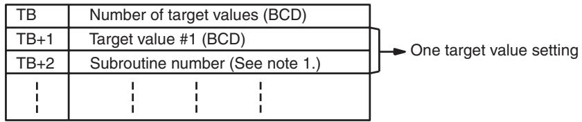
flowchart
graph TD
    A["TB"] --> B["Number of target values (BCD)"]
    C["TB+1"] --> D["Target value #1 (BCD)"]
    E["TB+2"] --> F["Subroutine number (See note 1.)"]
    G["..."] --> H["..."]
    I["..."] --> J["..."]
    K["..."] --> L["..."]
    M["..."] --> N["..."]
    O["..."] --> P["..."]
    Q["..."] --> R["..."]
    S["..."] --> T["..."]
    U["..."] --> V["..."]
    W["..."] --> X["..."]
    Y["..."] --> Z["..."]
    AA["..."] --> AB["..."]
    AC["..."] --> AD["..."]
    AE["..."] --> AF["..."]
    AG["..."] --> AH["..."]
    AI["..."] --> AJ["..."]
    AK["..."] --> AL["..."]
    AM["..."] --> AN["..."]
    AO["..."] --> AP["..."]
    AQ["..."] --> AR["..."]
    AS["..."] --> AT["..."]
    AU["..."] --> AV["..."]
    AW["..."] --> AX["..."]
    AY["One target value setting"] --> AZ
Note
- The subroutine number can be F000 to F255 to activate the subroutine when decrementing and can be 0000 to 0255 to activate the subroutine when incrementing.
- Allow an interval of at least 0.2 ms for interrupt processing when setting the target value for high-speed counters 1 and 2.
Target Value Comparison Operation
The following diagram illustrates the operation of target value comparisons for target values 1 through 5 set consecutively in the comparison table.
line
| Initial value | Count | | ------------- | ----- | | Target 1 | 0 | | Target 2 | 1 | | Target 3 | 2 | | Target 4 | 3 | | Target 5 | 4 |As illustrated above, the current count is compared with each target value in the order that they are registered in the target value comparison table. When the count is the same as the current target value, an interrupt is generated,
and comparison starts with the next target value. When all target values in the comparison table have been matched and interrupts for them generated, the target value is reset to the first target value in the table and the operation is repeated.
Range Comparison
A range comparison table contains 8 ranges which are defined by an 8-digit lower limit and an 8-digit upper limit, as well as their corresponding subroutine numbers. The corresponding subroutine is called and executed when the PV falls within a given range. (When interrupt processing is not required, an undefined subroutine number may be entered.)
flowchart
graph TD
    A["High-speed counter PV"] --> B["Lower limit 1 ↔ Upper limit 1"]
    A --> C["Lower limit 2 ↔ Upper limit 2"]
    A --> D["..."]
    A --> E["Lower limit 8 ↔ Upper limit 8"]
    B --> F["Execute subroutine."]
    C --> G["Execute subroutine."]
    E --> H["Execute subroutine."]
    style A fill:#f9f,stroke:#333
    style B fill:#ccf,stroke:#333
    style C fill:#ccf,stroke:#333
    style D fill:#ccf,stroke:#333
    style E fill:#ccf,stroke:#333
    style F fill:#dfd,stroke:#333
    style G fill:#dfd,stroke:#333
    style H fill:#dfd,stroke:#333
Always set 8 ranges. If fewer than 8 ranges are needed, set the remaining subroutine numbers to FFFF. If more than 8 ranges are needed, another comparison instruction such as BCMP(68) can be used to compare ranges with the high-speed counter PVs in IR 230 through IR 235. Bear in mind that these words are refreshed just once each cycle.
There are flags in the AR area which indicate when a high-speed counter's PV falls within one or more of the 8 ranges. The flags turn ON when a PV is within the corresponding range.
| Counter | AR area flags |
| High-speed counter 0 | AR 1100 to AR 1107 correspond to ranges 1 to 8. |
| High-speed counter 1 | AR 0500 to AR 0507 correspond to ranges 1 to 8. |
| High-speed counter 2 | AR 0600 to AR 0607 correspond to ranges 1 to 8. |
The following diagram shows the structure of a range comparison table for use with the CPU Unit's built-in high-speed counter 0 or the Pulse I/O Board's high-speed counters 1 or 2 set for linear counting.
flowchart
graph TD
    A["TB"] --> B["Lower limit #1, lower 4 digits (BCD)"]
    C["TB+1"] --> D["Lower limit #1, upper 4 digits (BCD)"]
    E["TB+2"] --> F["Upper limit #1, lower 4 digits (BCD)"]
    G["TB+3"] --> H["Upper limit #1, upper 4 digits (BCD)"]
    I["TB+4"] --> J["Subroutine number (See note 1.)"]
    K["TB+35"] --> L["Lower limit #8, lower 4 digits (BCD)"]
    M["TB+36"] --> N["Lower limit #8, upper 4 digits (BCD)"]
    O["TB+37"] --> P["Upper limit #8, lower 4 digits (BCD)"]
    Q["TB+38"] --> R["Upper limit #8, upper 4 digits (BCD)"]
    S["TB+39"] --> T["Subroutine number (See note 1.)"]
    U["First range setting"] --> V
    W["Eighth range setting"] --> X
The following diagram shows the structure of a range comparison table for use with the Pulse I/O Board's high-speed counters 1 or 2 set for ring counting. The ring value specifies the number of points in the ring and the maximum count value (ring value = max. count value + 1); the setting range fro the
ring value is 0 to 65,000. Do not change the ring value while a comparison is in progress.
The following diagram shows the structure of a range comparison table for use with the Absolute Encoder Interface Board's high-speed counters 1 and 2.

flowchart
graph TD
    A["TB"] --> B["Lower limit #1(BCD)"]
    C["TB+2"] --> D["Upper limit #1 (BCD)"]
    E["TB+4"] --> F["Subroutine number (See note 1.)"]
    G["TB+21"] --> H["Lower limit #8 (BCD)"]
    I["TB+22"] --> J["Upper limit #8 (BCD)"]
    K["TB+23"] --> L["Subroutine number (See note 1.)"]
    M["First range setting"] --> N
    O["Eighth range setting"] --> P
Note
- The subroutine number can be 0000 to 0255 and the subroutine will be executed as long as the counter's PV is within the specified range. A value of FFFF indicates that no subroutine is to be executed.
- Allow a time interval of at least 2 ms between the lower and upper limits (upper limit – lower limit > 0.002 × input pulse frequency) in range comparisons with high-speed counters 1 and 2.
The following table shows the possible values for target values, lower limit values, and upper limit values. The hexadecimal value F in the most significant digit indicates that the value is negative.
| Counter | Possible values |
| High-speed counter 0 (CPU Unit) | Differential phase mode: F003 2768 to 0003 2767Incrementing mode: 0000 0000 to 0006 5535 |
| High-speed counters 1 and 2 (Pulse I/O Board) | Linear counting: F838 8607 to 0838 8608Ring counting: 0000 0000 to 0006 4999 |
| Absolute high-speed counters 1 and 2 (Absolute Encoder Interface Board) | BCD mode: 0000 to 4095360° mode: 0000 to 0355 (5° units) |
In 360° mode the absolute high-speed counter's angular values are internally converted to binary values. The binary value after conversion depends on the resolution selected in the PC Setup (DM 6643 and/or DM 6644). The following table shows the converted values for 5° to 45°.
| Resolution | Converted value | ||||||||
| 5^ | 10^ | 15^ | 20^ | 25^ | 30^ | 35^ | 40^ | 45^ | |
| 8-bit (0 to 255) | 4 | 7 | 11 | 14 | 18 | 21 | 25 | 28 | 32 |
| 10-bit (0 to 1023) | 14 | 28 | 43 | 57 | 71 | 85 | 100 | 114 | 128 |
| 12-bit (0 to 4095) | 57 | 114 | 171 | 228 | 284 | 341 | 398 | 455 | 512 |
For higher values, find the converted value to the nearest 45^ and add the remainder from the table. For example, to convert 145^ into 8-bit resolution: 32 × 3 (for 135^ ) + 7 (for 10^ ) = 103.

With 10-bit and 12-bit resolution, interrupt processing might not be triggered when the angular value matches the comparison value because the converted values do not match exactly.
Range Comparison Operation
The following diagram illustrates the operation of range comparisons for range settings 1 through 4 set consecutively in the comparison table.
As illustrated above, the current count is compared against all the comparison ranges at the same time and the result for each range is output.
AR Area Flags
The following AR area flags indicate the status of comparison operations for high-speed counter 0 in the CPU Unit and high-speed counters 1 and 2 in the Pulse I/O Board or Absolute Encoder Interface Board.
| Word | Bit(s) | Operation |
| AR 05 | 00 to 07 | High-speed Counter 1 (Port 1) Range Comparison FlagsBits 00 to 07 will be turned ON when the counter PV is within the corresponding range (1 to 8). |
| 08 | High-speed Counter 1 (Port 1) Comparison FlagThis flag will be ON during PV comparison. | |
| 09 | High-speed Counter 1 (Port 1) Overflow/Underflow FlagThis flag will be ON when an overflow or underflow occurred. | |
| AR 06 | 00 to 07 | High-speed Counter 2 (Port 2) Range Comparison FlagsBits 00 to 07 will be turned ON when the counter PV is within the corresponding range (1 to 8). |
| 08 | High-speed Counter 2 (Port 2) Comparison FlagThis flag will be ON during PV comparison. | |
| 09 | High-speed Counter 2 (Port 2) Overflow/Underflow FlagThis flag will be ON when an overflow or underflow occurred. | |
| AR 11 | 00 to 07 | High-speed Counter 0 Range Comparison FlagsBits 00 to 07 will be turned ON when the counter PV is within the corresponding range (1 to 8). |
Operation with the High-speed Counter Board
When the execution condition is OFF, CTBL(63) is not executed. When the execution condition is ON, CTBL(63) registers a comparison table for use with the high-speed counter PV. Depending on the value of C, comparison with the high-speed counter PV can begin immediately or it can be started separately with INI(61).
The port specifier (P) specifies which one of the High-speed Counter Board's high-speed counters will be used in the comparison.
| Function | Port specifier (P) | |
| For a Board in slot 1 | For a Board in slot 2 | |
| High-speed counter 1 | 101 | 001 |
| High-speed counter 2 | 102 | 002 |
| High-speed counter 3 | 103 | 003 |
| High-speed counter 4 | 104 | 004 |
The function of CTBL(63) is determined by the control data, C, as shown in the following table. These functions are described after the table.
| C | CTBL(63) function |
| 000 | Registers a target value comparison table and starts comparison. |
| 001 | Registers a range comparison table and starts comparison. |
| 002 | Registers a target value comparison table. Start comparison with INI(61). |
| 003 | Registers a range comparison table. Start comparison with INI(61). |
When the PV agrees with a target value or falls within a specified range, a bit pattern is output to the allocated IR word. Refer to 1-4-6 High-speed Counter 0 Interrupts for more details on table comparison.
If the high-speed counter is enabled in the PC Setup (DM 6642), it will begin counting from zero when the CQM1H begins operation. The PV will not be compared to the comparison table until the table is registered and comparison is initiated with INI(61) or CTBL(63). Comparison can be stopped and started, or the PV can be reset with INI(61).
Once a comparison table has been registered, it is valid until the CQM1H is halted or until a error occurs in attempting to register a new table. The differentiated form of CTBL(63) is recommended when possible to reduce cycle time.
Target Value Comparison
Up to 48 target values can be registered. A bit pattern is also registered for each target value. The registered bit pattern is output to the allocated IR word when the PV matches a target value. The High-speed Counter Board does not generate interrupts; the registered bit pattern is reflected in the allocated IR word and at the external outputs.
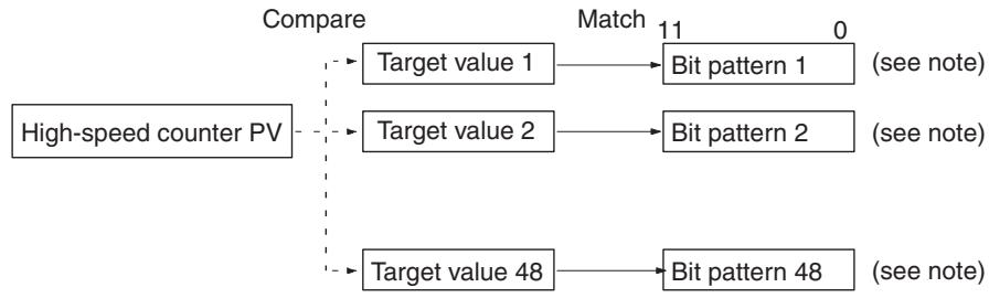
flowchart
graph TD
    A["High-speed counter PV"] --> B["Target value 1"]
    A --> C["Target value 2"]
    A --> D["Target value 48"]
    B --> E["Bit pattern 1 (see note)"]
    C --> F["Bit pattern 2 (see note)"]
    D --> G["Bit pattern 48 (see note)"]
    style A fill:#f9f,stroke:#333
    style B fill:#ccf,stroke:#333
    style C fill:#ccf,stroke:#333
    style D fill:#ccf,stroke:#333
    style E fill:#dfd,stroke:#333
    style F fill:#dfd,stroke:#333
    style G fill:#dfd,stroke:#333
Note Bit patterns 1 to 48 are configured as follows:
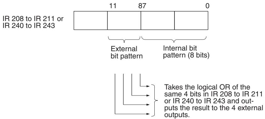
Target value comparisons are performed one item at a time in order of the comparison table. When the PV reaches the first target value in the table, the bit pattern is output to the allocated IR word and comparison continues to the next value in the table. When processing has been completed for the last target value in the table, comparison returns to the first value in the table and the process is repeated.
The following diagram shows the structure of a target value comparison table for use with high-speed counters 1 to 4 when set for linear counting.
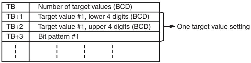
flowchart
graph TD
    A["TB"] --> B["Number of target values (BCD)"]
    C["TB+1"] --> D["Target value #1, lower 4 digits (BCD)"]
    E["TB+2"] --> F["Target value #1, upper 4 digits (BCD)"]
    G["TB+3"] --> H["Bit pattern #1"]
    I[" "] --> J[" "]
    K[" "] --> L[" "]
    M[" "] --> N[" "]
    O[" "] --> P[" "]
    Q[" "] --> R[" "]
    S[" "] --> T[" "]
    U[" "] --> V[" "]
    W[" "] --> X[" "]
    Y[" "] --> Z[" "]
    AA[" "] --> AB[" "]
    AC[" "] --> AD[" "]
    AE[" "] --> AF[" "]
    AG[" "] --> AH[" "]
    AI[" "] --> AJ[" "]
    AK[" "] --> AL[" "]
    AM[" "] --> AN[" "]
    AO[" "] --> AP[" "]
    AQ[" "] --> AR[" "]
    AS[" "] --> AT[" "]
    AU[" "] --> AV[" "]
    AW[" "] --> AX[" "]
    AY["One target value setting"] --> AZ
    style AY fill:#f9f,stroke:#333
    style AK fill:#f9f,stroke:#333
The following diagram shows the structure of a target value comparison table for use with high-speed counters 1 to 4 when set for ring counting. Input the target values in ascending or descending order.
The ring value specifies the number of points in the ring and the maximum count value (ring value = max. count value + 1). Do not change the ring value while a comparison is in progress.

flowchart
graph TD
    A["TB"] --> B["Ring value, lower 4 digits (BCD)"]
    C["TB+1"] --> D["Ring value, upper 4 digits (BCD)"]
    E["TB+2"] --> F["Number of target values (BCD)"]
    G["TB+3"] --> H["Target value #1, lower 4 digits (BCD)"]
    I["TB+4"] --> J["Target value #1, upper 4 digits (BCD)"]
    K["TB+5"] --> L["Bit pattern #1"]
    M[" "] --> N[" "]
    O[" "] --> P[" "]
    Q[" "] --> R[" "]
    S[" "] --> T[" "]
    U[" "] --> V[" "]
    W[" "] --> X[" "]
    Y[" "] --> Z[" "]
    AA[" "] --> AB[" "]
    AC[" "] --> AD[" "]
    AE[" "] --> AF[" "]
    AG[" "] --> AH[" "]
    AI[" "] --> AJ[" "]
    AK[" "] --> AL[" "]
    AM[" "] --> AN[" "]
    AO[" "] --> AP[" "]
    AQ[" "] --> AR[" "]
    AS[" "] --> AT[" "]
    AU[" "] --> AV[" "]
    AW[" "] --> AX[" "]
    AY[" "] --> AZ[" Ring value setting "]
    BA[" "] --> BB[" One target value setting "]
Target values 1 to 48 and bit patterns 1 to 48 are stored in the comparison table. Bits 0 to 7 of the bit pattern are stored as the internal bit pattern. Bits 8 to 11 are stored as the external bit pattern, the logical OR of these bits is calculated for the four high-speed counters, and the result is output to external outputs 1 to 4.
The following example shows how the bit patterns for high-speed counters 1 to 4 are ORed to produce the resulting output at the external outputs.
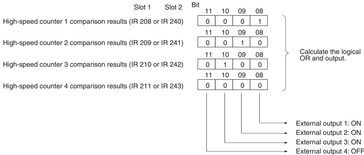
other
| Counter | Bit | Value | |---------|-----|-------| | High-speed counter 1 comparison results (IR 208 or IR 240) | 11 | 0 | | High-speed counter 1 comparison results (IR 208 or IR 240) | 10 | 0 | | High-speed counter 1 comparison results (IR 208 or IR 240) | 09 | 0 | | High-speed counter 1 comparison results (IR 208 or IR 240) | 08 | 1 | | High-speed counter 2 comparison results (IR 209 or IR 241) | 11 | 0 | | High-speed counter 2 comparison results (IR 209 or IR 241) | 10 | 0 | | High-speed counter 2 comparison results (IR 209 or IR 241) | 09 | 1 | | High-speed counter 2 comparison results (IR 209 or IR 241) | 08 | 0 | | High-speed counter 3 comparison results (IR 210 or IR 242) | 11 | 0 | | High-speed counter 3 comparison results (IR 210 or IR 242) | 10 | 0 | | High-speed counter 3 comparison results (IR 210 or IR 242) | 09 | 0 | | High-speed counter 3 comparison results (IR 210 or IR 242) | 08 | 0 | | High-speed counter 4 comparison results (IR 211 or IR 243) | 11 | 0 | | High-speed counter 4 comparison results (IR 211 or IR 243) | 10 | 0 | | High-speed counter 4 comparison results (IR 211 or IR 243) | 09 | 0 | | High-speed counter 4 comparison results (IR 211 or IR 243) | 08 | 0 | | High-speed counter 4 comparison results (IR 211 or IR 243) | 0 | 0 | The diagram illustrates the calculation of logical OR and output logic based on their respective bit allocations. The text below provides the labels for the outputs and functions.Target Value Comparison Operation
The following diagram illustrates the operation of target value comparisons for target values 1 through 5 set consecutively in the comparison table.
line
| Initial value | Count | | ------------- | ----- | | Target 1 | 0 | | Target 2 | 1 | | Target 3 | 2 | | Target 4 | 3 | | Target 5 | 4 |As illustrated above, the current count is compared with each target value in the order that they are registered in the target value comparison table. When the count is the same as the current target value, the registered bit pattern is output to the allocated IR word, and comparison starts with the next target value. When all target values in the comparison table have been matched and their bit patterns have been output, the target value is reset to the first target value in the table and the operation is repeated.
Range Comparison
A range comparison table contains 8 ranges which are defined by an 8-digit lower limit and an 8-digit upper limit, as well as the bit pattern. The registered bit pattern is output to the allocated IR word when the PV falls within a given range. The High-speed Counter Board does not generate interrupts; the registered bit pattern is reflected in the allocated IR word and at the external outputs.
flowchart
graph TD
    A["High-speed counter PV"] --> B["Lower limit 1 ↔ Upper limit 1"]
    A --> C["Lower limit 2 ↔ Upper limit 2"]
    A --> D["..."]
    A --> E["Lower limit 16 ↔ Upper limit 16"]
    B --> F["Bit pattern 1 (see note)"]
    C --> G["Bit pattern 2 (see note)"]
    E --> H["Bit pattern 16 (see note)"]
    style A fill:#f9f,stroke:#333
    style B fill:#ccf,stroke:#333
    style C fill:#ccf,stroke:#333
    style D fill:#ccf,stroke:#333
    style E fill:#ccf,stroke:#333
Note Bit patterns 1 to 16 are configured as follows:
Takes the logical OR of the same 4 bits in IR 208 to IR 211 or IR 240 to IR 243 and outputs the result to the 4 external outputs.
Register a lower limit, upper limit, and bit pattern for each range (1 to 16) in the range comparison table. Bits 0 to 7 of the bit pattern are stored as the internal bit pattern. Bits 8 to 11 are stored as the external bit pattern, the logical OR of these bits is calculated for the four high-speed counters, and the result is output to external outputs 1 to 4.
The following example shows how the bit patterns for high-speed counters 1 to 4 are ORed to produce the resulting output at the external outputs.
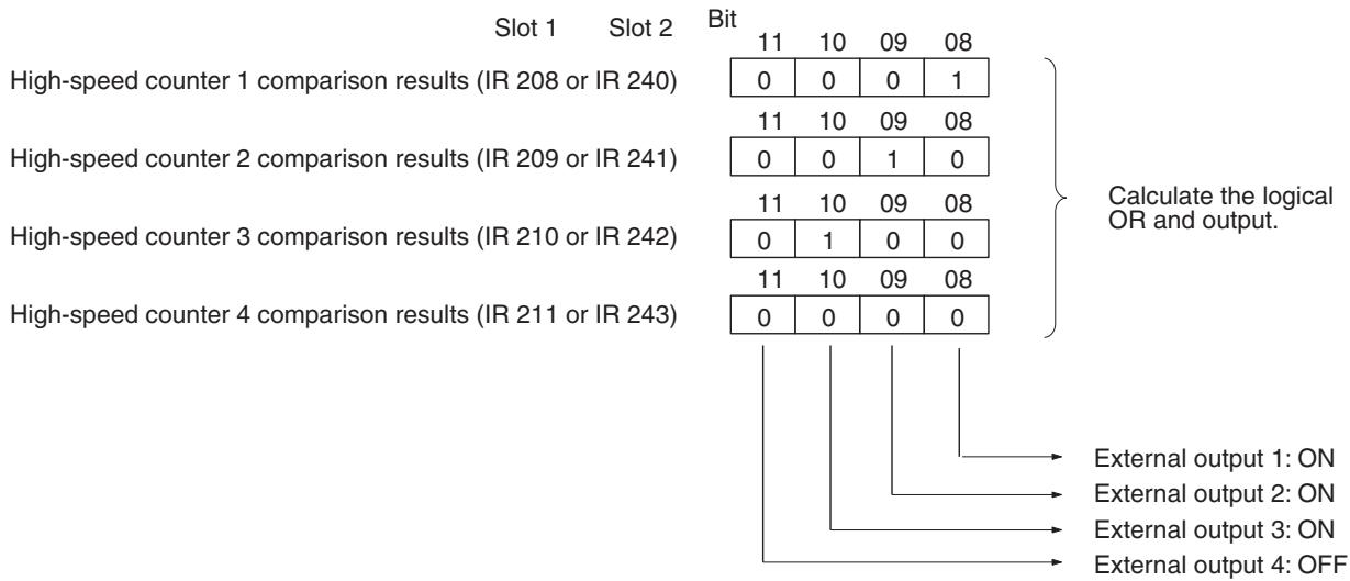
other
| Comparison Result | Bit | Value | | ----------------- | --- | ----- | | High-speed counter 1 | 11 | 10 | | High-speed counter 1 | 09 | 0 | | High-speed counter 1 | 08 | 1 | | High-speed counter 2 | 11 | 10 | | High-speed counter 2 | 09 | 0 | | High-speed counter 2 | 08 | 0 | | High-speed counter 3 | 11 | 10 | | High-speed counter 3 | 09 | 0 | | High-speed counter 3 | 08 | 0 | | High-speed counter 4 | 11 | 10 | | High-speed counter 4 | 09 | 0 | | High-speed counter 4 | 08 | 0 | The image contains a table of four rows of bits and logical output labels (e.g., 'External output 1: ON', 'External output 2: ON') with arrows pointing to the corresponding bits.The following diagram shows the structure of a range comparison table for use with high-speed counters 1 to 4 when set for linear counting.
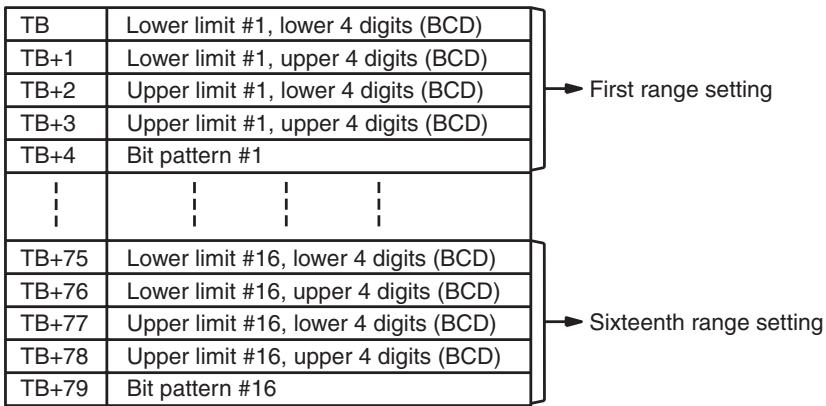
The following diagram shows the structure of a range comparison table for use with high-speed counters 1 to 4 when set for ring counting. The ring value specifies the number of points in the ring and the maximum count value (ring value = max. count value + 1). Do not change the ring value while a comparison is in progress.
The following table shows the possible values that can be set for high-speed counters 1 to 4 for target values, lower limit values, and upper limit values. The hexadecimal value F in the most significant digit indicates that the value is negative (a negative 7-digit value.)
| Data format | Possible values | |
| Linear counting | Ring counting | |
| BCD | F838 8608 to 0838 8607 | 0000 0001 to 0838 8607 |
| Hexadecimal | F800 0000 to 07FF FFFF | 0000 0001 to 07FF FFFF |
Range Comparison Operation
The following diagram illustrates the operation of range comparisons for range settings 1 through 4 set consecutively in the comparison table.
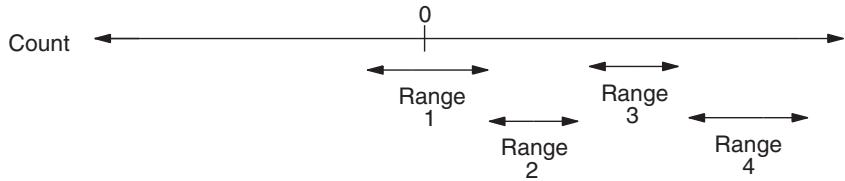
As illustrated above, the current count is compared against all the comparison ranges at the same time and the result for each range is output.
When the High-speed Counter Board is installed in slot 1, the bit patterns are output to IR 208 through IR 211. When the Board is installed in slot 2, the bit patterns are output to IR 240 through IR 243.
| Counter number | Allocated IR word | |
| For a Board in slot 1 | For a Board in slot 2 | |
| High-speed counter 1 | IR 208 | IR 240 |
| High-speed counter 2 | IR 209 | IR 241 |
| High-speed counter 3 | IR 210 | IR 242 |
| High-speed counter 4 | IR 211 | IR 243 |
The following table shows the function of the bits in the allocated IR word.
| Bit(s) | Function |
| 00 to 07 | Contains the internal bit pattern. |
| 08 to 11 | Contains the external bit pattern. |
| 12 | Counter Operating Flag (0: Stopped; 1: Operating) |
| 13 | Comparison Flag (0: Stopped; 1: Operating) |
| 14 | PV Overflow/Underflow Flag (0: Normal; 1: Overflow/underflow occurred) |
| 15 | SV Error Flag (0: Normal; 1: SV error occurred) |
Note
- When using target comparison for high-speed counters 1 to 4, set the target values so that bit patterns are output at an interval of 0.2 ms or greater.
- When using range comparison for high-speed counters 1 to 4, set the limits so that the PV of the counter remains between the upper and lower limit for 0.5 ms or greater. (Upper limit – Lower limit > 0.0005 x Input frequency)
- When using target comparison for high-speed counters 1 to 4, it does not matter if the target value is reach by incrementing or decrementing. This is also true for target value comparison for the High-speed Counter Board, but is different from high-speed counters 1 and 2 in Ring Mode on the Pulse I/O Board or high-speed counters 1 and 2 on the Absolute Encoder Interface Board.
High-speed counters 1 to 4 begin counting from 0 when CQM1H program operation begins, but the bit pattern will not be output until comparison begins. Use INI(61) to stop comparison.
A comparison table registered with CTBL(63) is valid until CQM1H program operation ends or a different comparison table is registered. The cycle time can be reduced by executing a differentiated variation of CTBL(63) when required.
Flags
ER: The specified port and function are not compatible.
There is another CTBL(63) instruction with a different comparison method in the subroutine called by CTBL(63) instruction.
A CTBL(63) instruction with a different comparison method is executed during comparison.
Indirectly addressed EM/DM word is non-existent.
(Content of *EM/*DM word is not BCD, or the EM/DM area boundary has been exceeded.)
The comparison table exceeds the data area boundary, or there is an error in the comparison table settings.
CTBL(63) is executed in an interrupt subroutine while a pulse I/O or high-speed counter instruction is being executed in the main program.
Subroutines or bit pattern output is executed only once when the execution conditions are first met. AR status is refreshed only once per cycle. If conditions are met for more than one item in the table at the same time, the first item in the table takes priority.
5-16-8 MODE CONTROL - INI(61)
Ladder Symbols
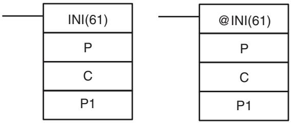
flowchart
graph TD
    A["INI(61)"] --> B["P"]
    A --> C["C"]
    A --> D["P1"]
    E["@INI(61)"] --> F["P"]
    E --> G["C"]
    E --> H["P1"]
Operand Data Areas
| P: Port specifier |
| 000 to 004 or 101 to 104 |
| C: Control data |
| 000 to 003 |
| P1: First PV word |
| IR, SR, AR, DM, EM, HR, LR |
Limitations
P1 must be 000 unless C is 002.
P1 and P1+1 must be in the same data area.
DM 6143 to DM 6655 cannot be used for P1.
Description
INI(61) can be used with the functions listed in the following table.
| Unit/Board | Function |
| CPU Unit | High-speed counter 0 (IR 00004 to IR 00006) |
| Transistor Output Unit | Pulse outputs |
| Pulse I/O Board | High-speed counters 1 and 2Pulse outputs 1 and 2 |
| Absolute Encoder Interface Board | Absolute high-speed counters 1 and 2 |
| High-speed Counter Board | High-speed counters 1 to 4 |
When the execution condition is OFF, INI(61) is not executed. When the execution condition is ON, INI(61) is used to control high-speed counter operation and stop pulse output.
The port specifier (P) specifies the high-speed counter or pulse output that will be controlled.
| Unit | Function | Port specifier (P) |
| CPU Unit | High-speed counter 0 | 000 |
| Transistor Output Unit | Pulse output | 000 |
| Inner Board | Function | Port specifier (P) | |
| Slot 1 | Slot 2 | ||
| Pulse I/O Board | High-speed counter 1 or pulse output 1 | --- | 001 |
| High-speed counter 2 or pulse output 2 | --- | 002 | |
| Absolute Encoder Interface Board | Absolute high-speed counter 1 | --- | 001 |
| Absolute high-speed counter 2 | --- | 002 | |
| High-speed Counter Board | High-speed counter 1 | 101 | 001 |
| High-speed counter 2 | 102 | 002 | |
| High-speed counter 3 | 103 | 003 | |
| High-speed counter 4 | 104 | 004 | |
The function of INI(61) is determined by the control data, C. (P1 and P1+1 contain the new high-speed counter PV when changing the PV.)
| C | P1 | INI(61) function |
| 000 | 000 | Starts CTBL(63) table comparison. |
| 001 | 000 | Stops CTBL(63) table comparison. |
| 002 | New high-speed counter PV | Changes high-speed counter PV. |
| 003 | 000 | Stops pulse output. |
The following table shows which values of C can be used with each function.
| Unit/Board | Function | Values of C | |||
| 000 | 001 | 002 | 003 | ||
| CPU Unit | High-speed counter 0 | YES | YES | YES | --- |
| Transistor Output Unit | Pulse output | --- | --- | --- | YES |
| Pulse I/O Board | High-speed counters 1 and 2 | YES | YES | YES | --- |
| Pulse outputs 1 and 2 | --- | --- | --- | YES | |
| Absolute Encoder Interface Board | Absolute high-speed counters 1 and 2 | YES | YES | --- | --- |
| High-speed Counter Board | High-speed counters 1 to 4 | YES | YES | YES | --- |
CTBL(63) Table Comparison
PV Change
If C is 000 or 001, INI(61) starts or stops comparison of the high-speed counter's PV to the comparison table registered with CTBL(63). Refer to 1-4-6 High-speed Counter 0 Interrupts for details on table comparison.
If C is 002, INI(61) changes the high-speed counter's PV to the 8-digit value in P1 and P1+1. The leftmost 4 digits are stored in P1+1 and the rightmost 4 digits are stored in P1. A hexadecimal value of F in the most significant digit of PV indicates that the PV is negative.
CPU Unit: Built-in High-speed Counter 0
The following table shows the possible 8-digit BCD values for the PV of high-speed counter 0.
| Mode | Possible values |
| Differential phase mode | F003 2768 to 0003 2767 |
| Incrementing mode | 0000 0000 to 0006 5535 |
Pulse I/O Board: High-speed Counters 1 and 2
The following table shows the possible 8-digit BCD values for the PV of high-speed counters 1 and 2 on a Pulse I/O Board.
| Numeric range | Possible values |
| Linear counting | F838 8608 to 0838 8607 |
| Ring counting | 0000 0000 to 0006 4999 |
Absolute Encoder Interface Board: High-speed Counters 1 and 2
The PV of absolute high-speed counters 1 and 2 cannot be changed.
High-speed Counter Board: High-speed Counters 1 to 4
The following table shows the possible 8-digit values (BCD or hexadecimal) for the PV of high-speed counters 1 to 4 on a High-speed Counter Board.
| Numeric range | Possible values | |
| BCD format | Hexadecimal format | |
| Linear counting | F838 8608 to 0838 8607 | F800 0000 to 07FF FFFF |
| Ring counting | 0000 0000 to 0838 8607 | 0000 0000 to 07FF FFFF |
Stop Pulse Output
If C is 003, INI(61) stops pulse output. Refer to 1-5 Pulse Output Function for details on stopping Pulse I/O Board pulse outputs 1 and 2.
Note Pulse output can be stopped only when pulses are not currently being output. The Pulse Output Flag (AR 0515 or AR 0615) can be used to check pulse output status.
Flags
ER: The specified port and function are not compatible.
Indirectly addressed EM/DM word is non-existent.
(Content of *EM/*DM word is not BCD, or the EM/DM area boundary has been exceeded.)
P1+1 exceeds the data area boundary. (C=002)
There is an error in the operand settings.
INI(61) is executed in an interrupt subroutine while a pulse I/O or high-speed counter instruction is being executed in the main program.
5-16-9 HIGH-SPEED COUNTER PV READ – PRV(62)
Ladder Symbols
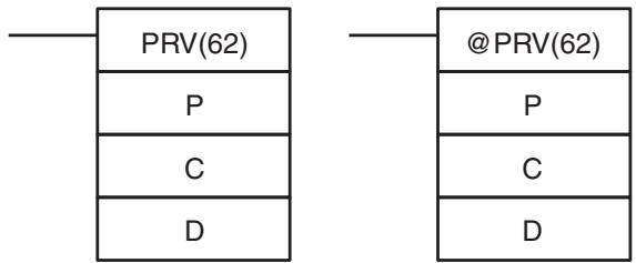
flowchart
graph TD
    A["PRV(62)"] --> B["P"]
    A --> C["C"]
    A --> D["D"]
    E["@PRV(62)"] --> F["P"]
    E --> G["C"]
    E --> H["D"]
Operand Data Areas
| P: Port specifier |
| 000 to 004 or 101 to 104 |
| C: Control data |
| 000 to 004 or 101 to 104 |
| D: First destination word |
| IR, SR, AR, DM, EM, HR, LR |
Limitations
ID and D+1 must be in the same data area.
DM 6143 to DM 6655 cannot be used for D.
Description
PRV(62) can be used with the functions listed in the following table.
| Unit/Board | Function |
| CPU Unit | High-speed counter 0 (IR 00004 to IR 00006) |
| Pulse I/O Board | High-speed counters 1 and 2Pulse outputs 1 and 2 |
| Absolute Encoder Interface Board | Absolute high-speed counters 1 and 2 |
| High-speed Counter Board | High-speed counters 1 to 4 |
When the execution condition is OFF, PRV(62) is not executed. When the execution condition is ON, PRV(62) reads data specified by P and C and writes it to D or D and D+1.
The port specifier (P) specifies the high-speed counter or pulse output that will be controlled.
| Unit | Function | Port specifier (P) | |
| CPU Unit | High-speed counter 0 | 000 | |
| Transistor Output Unit | Pulse output | 000 | |
| Inner Board | Function | Port specifier (P) | |
| Slot 1 | Slot 2 | ||
| Pulse I/O Board | High-speed counter 1 or pulse output 1 | --- | 001 |
| High-speed counter 2 or pulse output 2 | --- | 002 | |
| Absolute Encoder Interface Board | Absolute high-speed counter 1 | --- | 001 |
| Absolute high-speed counter 2 | --- | 002 | |
| High-speed Counter Board | High-speed counter 1 | 101 | 001 |
| High-speed counter 2 | 102 | 002 | |
| High-speed counter 3 | 103 | 003 | |
| High-speed counter 4 | 104 | 004 | |
The control data, C, determines which type of data will be accessed.
| C | Data | Destination word(s) |
| 000 | High-speed counter PV | D and D+1 |
| 001 | Status of high-speed counter or pulse output | D |
| 002 | Range comparison results | D |
The following table shows which values of C can be used with each function.
| Unit/Board | Function | Values of C | ||
| 000 | 001 | 002 | ||
| CPU Unit | High-speed counter 0 | YES | --- | --- |
| Transistor Output Unit | Pulse output | --- | --- | --- |
| Pulse I/O Board | High-speed counters 1 and 2 | YES | YES | YES |
| Pulse outputs 1 and 2 | --- | YES | --- | |
| Absolute Encoder Interface Board | Absolute high-speed counters 1 and 2 | YES | YES | YES |
| High-speed Counter Board | High-speed counters 1 to 4 | YES | YES | --- |
High-speed Counter PV (C=000)
If C is 000, PRV(62) reads the specified high-speed counter's PV and writes the 8-digit value in D and D+1. The leftmost 4 digits are stored in D+1 and the rightmost 4 digits are stored in D. A hexadecimal value of F in the most significant digit of PV indicates that the PV is negative.
PRV(62) reads the same high-speed counter PV information stored in the IR words allocated for that purpose (IR 230 and IR 231 for high-speed counter 0, IR 200 to IR 207 or IR 232 to IR 239 for high-speed counters 1 to 4), but the allocated IR words are refreshed just once each cycle while PRV(62) reads the most up-to-date values.
CPU Unit: Built-in High-speed Counter 0
The following table shows the possible 8-digit BCD values for the PV of high-speed counter 0.
| Mode | Possible values |
| Differential phase mode | F003 2768 to 0003 2767 |
| Incrementing mode | 0000 0000 to 0006 5535 |
Pulse I/O Board: High-speed Counters 1 and 2
The following table shows the possible 8-digit BCD values for the PV of high-speed counters 1 and 2 on a Pulse I/O Board.
| Numeric range | Possible values |
| Linear counting | F838 8608 to 0838 8607 |
| Ring counting | 0000 0000 to 0006 4999 |
Absolute Encoder Interface Board: High-speed Counters 1 and 2
The following table shows the possible values for the PV of absolute high-speed counters 1 and 2.
| Mode | Possible values |
| BCD mode | 0000 0000 to 0000 4095 |
| 360° mode | 0000 0000 to 0000 0359 |
High-speed Counter Board: High-speed Counters 1 to 4
The following table shows the possible 8-digit values (BCD or hexadecimal) for the PV of high-speed counters 1 to 4 on a High-speed Counter Board.
| Numeric range | Possible values | |
| BCD format | Hexadecimal format | |
| Linear counting | F838 8608 to 0838 8607 | F800 0000 to 07FF FFFF |
| Ring counting | 0000 0000 to 0838 8607 | 0000 0000 to 07FF FFFF |
High-speed Counter or Pulse Output Status (C=001)
If C is 001, PRV(62) reads the operating status of the specified high-speed counter or pulse output and writes the data to D.
PRV(62) reads the same information stored in the AR and IR words allocated for that purpose (AR 05 and AR 06 for the Pulse I/O Board or Absolute Encoder Interface Board, IR 208 to IR 211 or IR 240 to IR 243 for the High-speed Counter Board), but the allocated AR and IR words are refreshed just once each cycle while PRV(62) reads the most up-to-date values.
Pulse I/O Board
The following table shows the function of bits in D for high-speed counters 1 and 2 or pulse outputs from ports 1 and 2 on a Pulse I/O Board. Bits not listed in the table are not used and will always be 0.
| Bit | Function |
| 00 | High-speed counter comparison status. (0: Stopped; 1: Comparing) |
| 01 | High-speed counter underflow/overflow.(0: Normal; 1: Underflow/Overflow occurred.) |
| 04 | Deceleration of pulse frequency. (0: Not specified; 1: Specified.) |
| 05 | Total number of pulses specified. (0: Not specified; 1: Specified.) |
| 06 | Pulse output completed. (0: Not completed; 1: Completed) |
| 07 | Pulse output status (0: Stopped; 1: Outputting) |
Absolute Encoder Interface Board
For absolute high-speed counters 1 and 2, Bit 00 of D indicates the comparison status (0: Stopped; 1: Comparing). The other bits in D (01 through 15) are not used and will always be 0.
High-speed Counter Board
The following table shows the function of bits in D for high-speed counters 1 to 4 on a High-speed Counter Board.
| Bit(s) | Function |
| 00 to 07 | Contains the internal bit pattern. |
| 08 to 11 | Contains the external bit pattern. |
| 12 | Counter Operating Flag (0: Stopped; 1: Operating) |
| 13 | Comparison Flag (0: Stopped; 1: Operating) |
| 14 | PV Overflow/Underflow Flag (0: Normal; 1: Overflow/underflow occurred) |
| 15 | SV Error Flag (0: Normal; 1: SV error occurred) |
Range Comparison Results (C=002)
If C is 002, PRV(62) reads the results of the range comparison results for Pulse I/O Board high-speed counters 1 and 2, or Absolute Encoder Interface Board absolute high-speed counters 1 and 2.
Bits 00 through 07 of D contain the Comparison Result flags for ranges 1 to 8. (0: Not in range; 1: In range)
PRV(62) reads the same information stored in the AR words allocated for that purpose (AR 05 and AR 06 for the Pulse I/O Board or Absolute Encoder Interface Board), but the allocated AR words are refreshed just once each cycle while PRV(62) reads the most up-to-date values.
Flags
ER: The specified port and function are not compatible.
Indirectly addressed EM/DM word is non-existent.
(Content of *EM/*DM word is not BCD, or the EM/DM area boundary has been exceeded.)
D+1 exceeds the data area boundary. (C=000)
There is an error in the operand settings.
PRV(62) is executed in an interrupt subroutine while a pulse I/O or high-speed counter instruction is being executed in the main program.
5-17 Shift Instructions
5-17-1 SHIFT REGISTER - SFT(10)
Ladder Symbol
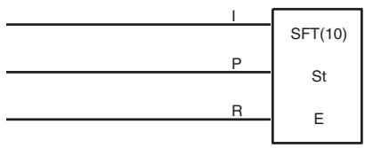
Operand Data Areas
| St: Starting word |
| IR, SR, AR, HR, LR |
| E: End word |
| IR, SR, AR, HR, LR |
Limitations
E must be greater than or equal to St, and St and E must be in the same data area.
If a bit address in one of the words used in a shift register is also used in an instruction that controls individual bit status (e.g., OUT, KEEP(11)), an error ("COIL/OUT DUPL") will be generated when program syntax is checked on the Programming Console or another Programming Device. The program, however, will be executed as written. See Example 2: Controlling Bits in Shift Registers for a programming example that does this.
Description
SFT(10) is controlled by three execution conditions, I, P, and R. If SFT(10) is executed and 1) execution condition P is ON and was OFF in the last execution, and 2) R is OFF, then execution condition I is shifted into the rightmost bit of a shift register defined between St and E, i.e., if I is ON, a 1 is shifted into the register; if I is OFF, a 0 is shifted in. When I is shifted into the register, all bits previously in the register are shifted to the left and the leftmost bit of the register is lost.
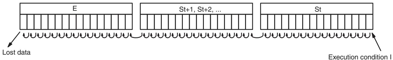
flowchart
graph LR
    A["Lost data"] --> B["E"]
    B --> C["St+1, St+2, ..."]
    C --> D["St"]
    D --> E["Execution condition I"]
The execution condition on P functions like a differentiated instruction, i.e., I will be shifted into the register only when P is ON and was OFF the last time SFT(10) was executed. If execution condition P has not changed or has gone from ON to OFF, the shift register will remain unaffected.
St designates the rightmost word of the shift register; E designates the leftmost. The shift register includes both of these words and all words between them. The same word may be designated for St and E to create a 16-bit (i.e., 1-word) shift register.
When execution condition R goes ON, all bits in the shift register will be turned OFF (i.e., set to 0) and the shift register will not operate until R goes OFF again.
Flags
There are no flags affected by SFT(10).
Example
The following example uses the 1-second clock pulse bit (25502) so that the execution condition produced by 00000 is shifted into IR 010 every second. Output 10000 is turned ON whenever a "1" is shifted into 01007.
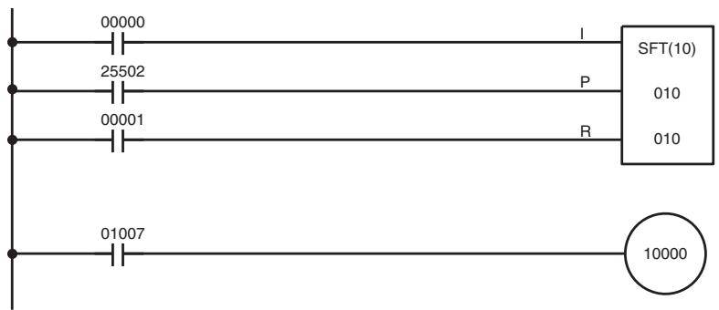
| Address | Instruction | Operands |
| 00000 | LD | 00000 |
| 00001 | LD | 25502 |
| 00002 | LD | 00001 |
| 00003 | SFT(10) | 010 |
| 010 | ||
| 00004 | LD | 01007 |
| 00005 | OUT | 10000 |
5-17-2 WORD SHIFT – WSFT(16)
Ladder Symbols
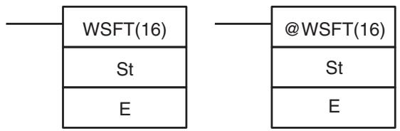
flowchart
graph TD
    A["WSFT(16)"] --> B["St"]
    A --> C["E"]
    D["@WSFT(16)"] --> E["St"]
    D --> F["E"]
Operand Data Areas
| St: Starting word |
| IR, SR, AR, DM, EM, HR, LR |
| E: End word |
| IR, SR, AR, DM, EM, HR, LR |
Limitations
St and E must be in the same data area, and E must be greater than or equal to St.
DM 6144 to DM 6655 cannot be used for St or E.
Description
When the execution condition is OFF, WSFT(16) is not executed. When the execution condition is ON, WSFT(16) shifts data between St and E in word units. Zeros are written into St and the content of E is lost.
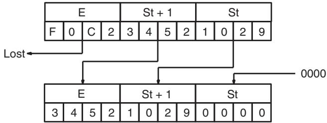
flowchart
graph TD
    A["E"] --> B["St + 1"]
    B --> C["St"]
    D["F 0 C 2 3 4 5 2 1 0 2 9"] --> E["E"]
    F["0000"] --> E
    E --> G["St + 1"]
    G --> H["St"]
    I["Lost"] --> A
    I --> F
    style A fill:#f9f,stroke:#333
    style B fill:#f9f,stroke:#333
    style C fill:#f9f,stroke:#333
    style D fill:#ccf,stroke:#333
    style E fill:#ccf,stroke:#333
    style F fill:#ccf,stroke:#333
    style G fill:#ccf,stroke:#333
    style H fill:#ccf,stroke:#333
Flags
ER: The St and E words are in different areas, or St is greater than E.
Indirectly addressed EM/DM word is non-existent.
(Content of *EM/*DM word is not BCD, or the EM/DM area boundary has been exceeded.)
5-17-3 ARITHMETIC SHIFT LEFT - ASL(25)
Ladder Symbols
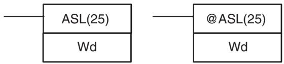
flowchart
graph LR
    A["ASL(25)"] --> B["Wd"]
    C["@ASL(25)"] --> D["Wd"]
Operand Data Areas

Limitations
DM 6144 to DM 6655 cannot be used for Wd.
Description
When the execution condition is OFF, ASL(25) is not executed. When the execution condition is ON, ASL(25) shifts a 0 into bit 00 of Wd, shifts the bits of Wd one bit to the left, and shifts the status of bit 15 into CY.
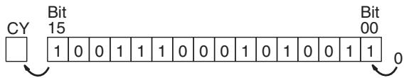
Precautions
A 0 will be shifted into bit 00 every cycle if the undifferentiated form of ASL(25) is used. Use the differentiated form (@ASL(25)) or combine ASL(25) with DIFU(13) or DIFD(14) to shift just one time.
Flags
ER: Indirectly addressed EM/DM word is non-existent.
(Content of *EM/*DM word is not BCD, or the EM/DM area boundary has been exceeded.)
CY: Receives the status of bit 15.
EQ: ON when the content of Wd is zero; otherwise OFF.
5-17-4 ARITHMETIC SHIFT RIGHT - ASR(26)
Ladder Symbols
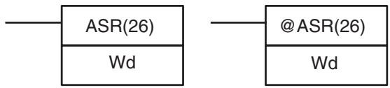
flowchart
graph LR
    A["ASR(26)"] --> B["Wd"]
    C["@ASR(26)"] --> D["Wd"]
Operand Data Areas
| Wd: Shift word |
| IR, SR, AR, DM, EM, HR, LR |
Limitations
DM 6144 to DM 6655 cannot be used for Wd.
Description
When the execution condition is OFF, ASR(25) is not executed. When the execution condition is ON, ASR(25) shifts a 0 into bit 15 of Wd, shifts the bits of Wd one bit to the right, and shifts the status of bit 00 into CY.
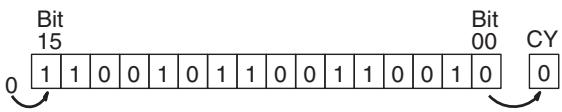
Precautions
A 0 will be shifted into bit 15 every cycle if the undifferentiated form of ASR(26) is used. Use the differentiated form (@ASR(26)) or combine ASR(26) with DIFU(13) or DIFD(14) to shift just one time.
Flags
ER :Indirectly addressed EM/DM word is non-existent.
(Content of *EM/*DM word is not BCD, or the EM/DM area boundary has been exceeded.)
CY: Receives the data of bit 00.
EQ: ON when the content of Wd is zero; otherwise OFF.
5-17-5 ROTATE LEFT - ROL(27)
Ladder Symbols
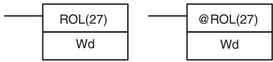
flowchart
graph LR
    A["ROL(27)"] --> B["Wd"]
    C["@ROL(27)"] --> D["Wd"]
Operand Data Areas
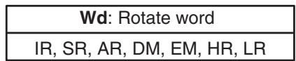
Limitations
DM 6144 to DM 6655 cannot be used for Wd.
Description
When the execution condition is OFF, ROL(27) is not executed. When the execution condition is ON, ROL(27) shifts all Wd bits one bit to the left, shifting CY into bit 00 of Wd and shifting bit 15 of Wd into CY.
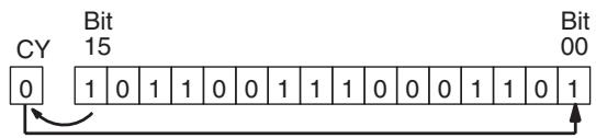
Precautions
Use STC(41) to set the status of CY or CLC(41) to clear the status of CY before doing a rotate operation to ensure that CY contains the proper status before executing ROL(27).
CY will be shifted into bit 00 every cycle if the undifferentiated form of ROL(27) is used. Use the differentiated form (@ROL(27)) or combine ROL(27) with DIFU(13) or DIFD(14) to shift just one time.
Flags
ER: Indirectly addressed EM/DM word is non-existent.
(Content of *EM/*DM word is not BCD, or the EM/DM area boundary has been exceeded.)
CY: Receives the data of bit 15.
EQ: ON when the content of Wd is zero; otherwise OFF.
5-17-6 ROTATE RIGHT - ROR(28)
Ladder Symbols
flowchart
graph LR
    A["ROR(28)"] --> B["Wd"]
    C["@ROR(28)"] --> D["Wd"]
Operand Data Areas
Limitations
DM 6144 to DM 6655 cannot be used for Wd.
Description
When the execution condition is OFF, ROR(28) is not executed. When the execution condition is ON, ROR(28) shifts all Wd bits one bit to the right, shifting CY into bit 15 of Wd and shifting bit 00 of Wd into CY.
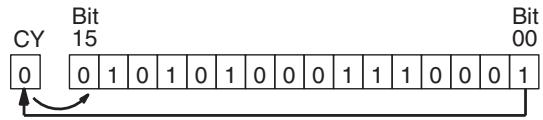
Precautions
Use STC(41) to set the status of CY or CLC(41) to clear the status of CY before doing a rotate operation to ensure that CY contains the proper status before execution ROR(28).
CY will be shifted into bit 15 every cycle if the undifferentiated form of ROR(28) is used. Use the differentiated form (@ROR(28)) or combine ROR(28) with DIFU(13) or DIFD(14) to shift just one time.
Flags
ER: Indirectly addressed EM/DM word is non-existent.
(Content of *EM/*DM word is not BCD, or the EM/DM area boundary has been exceeded.)
CY: Receives the data of bit 00.
EQ: ON when the content of Wd is zero; otherwise OFF.
5-17-7 ONE DIGIT SHIFT LEFT - SLD(74)
Ladder Symbols
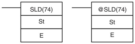
flowchart
graph TD
    A["SLD(74)"] --> B["St"]
    A --> C["E"]
    D["@SLD(74)"] --> E["St"]
    D --> F["E"]
Operand Data Areas
| St: Starting word |
| IR, SR, AR, DM, EM, HR, LR |
| E: End word |
| IR, SR, AR, DM, EM, HR, LR |
Limitations
St and E must be in the same data area, and E must be greater than or equal to St.
DM 6144 to DM 6655 cannot be used for St or E.
Description
When the execution condition is OFF, SLD(74) is not executed. When the execution condition is ON, SLD(74) shifts data between St and E (inclusive) by one digit (four bits) to the left. 0 is written into the rightmost digit of the St, and the content of the leftmost digit of E is lost.

Precautions
If a power failure occurs during a shift operation across more than 50 words, the shift operation might not be completed.
A 0 will be shifted into the least significant digit of St every cycle if the undifferentiated form of SLD(74) is used. Use the differentiated form (@SLD(74)) or combine SLD(74) with DIFU(13) or DIFD(14) to shift just one time.
Flags
ER: The St and E words are in different areas, or St is greater than E.
Indirectly addressed EM/DM word is non-existent.
(Content of *EM/*DM word is not BCD, or the EM/DM area boundary has been exceeded.)
5-17-8 ONE DIGIT SHIFT RIGHT – SRD(75)
Ladder Symbols
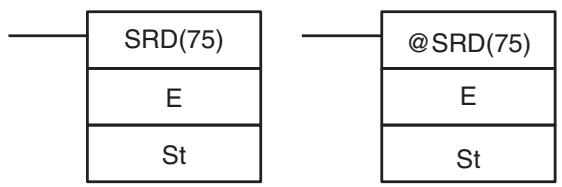
flowchart
graph TD
    A["SRD(75)"] --> B["E"]
    A --> C["St"]
    D["@SRD(75)"] --> E["E"]
    D --> F["St"]
Operand Data Areas
| E: End word |
| IR, SR, AR, DM, EM, HR, LR |
| St: Starting word |
| IR, SR, AR, DM, EM, HR, LR |
Limitations
St and E must be in the same data area, and E must be less than or equal to St.
DM 6144 to DM 6655 cannot be used for St or E.
Description
When the execution condition is OFF, SRD(75) is not executed. When the execution condition is ON, SRD(75) shifts data between St and E (inclusive) by one digit (four bits) to the right. 0 is written into the leftmost digit of St and the rightmost digit of E is lost.
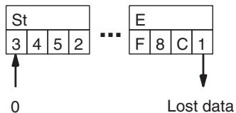
Precautions
If a power failure occurs during a shift operation across more than 50 words, the shift operation might not be completed.
A 0 will be shifted into the most significant digit of St every cycle if the undifferentiated form of SRD(75) is used. Use the differentiated form (@SRD(75)) or combine SRD(75) with DIFU(13) or DIFD(14) to shift just one time.
Flags
ER: The St and E words are in different areas, or St is less than E.
Indirectly addressed EM/DM word is non-existent.
(Content of *EM/*DM word is not BCD, or the EM/DM area boundary has been exceeded.)
5-17-9 REVERSIBLE SHIFT REGISTER – SFTR(84)
Ladder Symbols
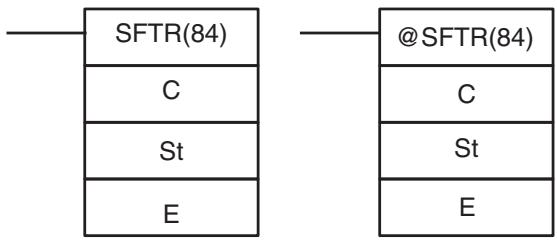
flowchart
graph TD
    A["SFTR(84)"] --> B["C"]
    A --> C["St"]
    A --> D["E"]
    E["@SFTR(84)"] --> F["C"]
    E --> G["St"]
    E --> H["E"]
Operand Data Areas
| C: Control word |
| IR, SR, AR, DM, EM, HR, LR |
| St: Starting word |
| IR, SR, AR, DM, EM, HR, LR |
| E: End word |
| IR, SR, AR, DM, EM, HR, LR |
Limitations
St and E must be in the same data area and St must be less than or equal to E.
DM 6144 to DM 6655 cannot be used for C, St, or E.
Description
SFTR(84) is used to create a single- or multiple-word shift register that can shift data to either the right or the left. To create a single-word register, designate the same word for St and E. The control word provides the shift direction, the status to be put into the register, the shift pulse, and the reset input. The control word is allocated as follows:
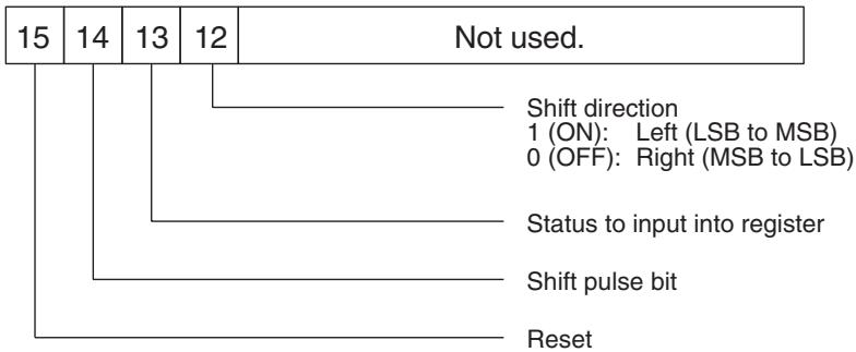
flowchart
graph TD
    A["15"] --> B["Shift direction"]
    A --> C["Status to input into register"]
    A --> D["Shift pulse bit"]
    A --> E["Reset"]
    B --> F["1 (ON): Left (LSB to MSB)"]
    B --> G["0 (OFF): Right (MSB to LSB)"]
The data in the shift register will be shifted one bit in the direction indicated by bit 12, shifting one bit out to CY and the status of bit 13 into the other end whenever SFTR(84) is executed with an ON execution condition as long as the reset bit is OFF and as long as bit 14 is ON. If SFTR(84) is executed with an OFF execution condition or if SFTR(84) is executed with bit 14 OFF, the shift register will remain unchanged. If SFTR(84) is executed with an ON execution condition and the reset bit (bit 15) is OFF, the entire shift register and CY will be set to zero.
Flags
ER: St and E are not in the same data area or ST is greater than E.
Indirectly addressed EM/DM word is non-existent.
(Content of *EM/*DM word is not BCD, or the EM/DM area boundary has been exceeded.)
CY: Receives the status of bit 00 of St or bit 15 of E, depending on the shift direction.
Example
In the following example, IR 00000, IR 00001, IR 00002, and IR 00003 are used to control the bits of C used in @SFTR(84). The shift register is in DM 0010, and it is controlled through IR 00004.
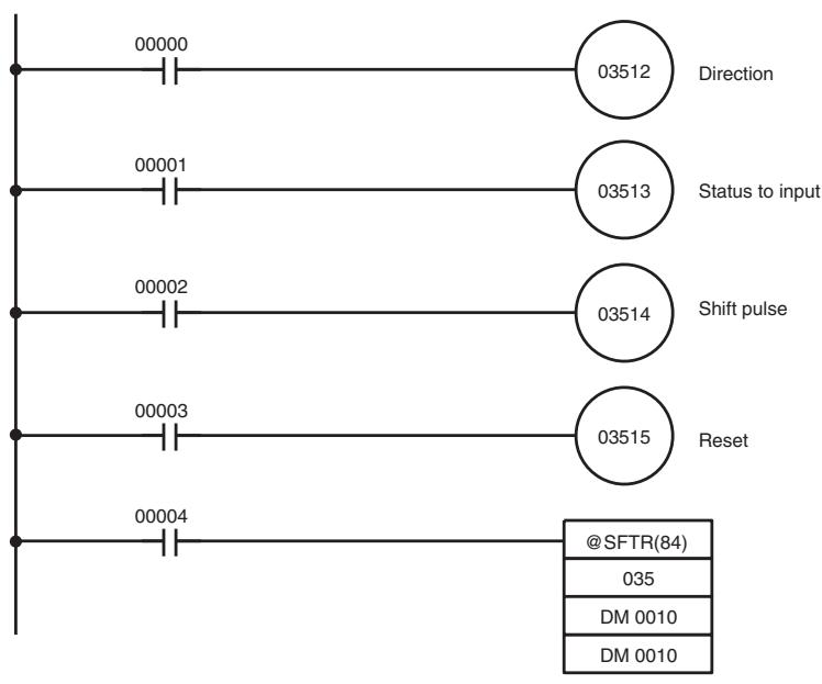
flowchart
graph TD
    A["00000"] --> B["03512"]
    C["00001"] --> D["03513"]
    E["00002"] --> F["03514"]
    G["00003"] --> H["03515"]
    I["00004"] --> J["@SFTR(84)"]
    K["Direction"] --> L["035"]
    M["Status to input"] --> N["03513"]
    O["Shift pulse"] --> P["03514"]
    Q["Reset"] --> R["03515"]
    S["DM 0010"] --> T["035"]
    U["DM 0010"] --> V["035"]
| Address | Instruction | Operands |
| 00000 | LD | 00000 |
| 00001 | OUT | 03512 |
| 00002 | LD | 00001 |
| 00003 | OUT | 03513 |
| 00004 | LD | 00002 |
| 00005 | OUT | 03514 |
| 00006 | LD | 00003 |
| 00007 | OUT | 03515 |
| 00008 | LD | 00004 |
| 00009 | @SFT(10) | |
| 035 | ||
| DM 0010 | ||
| DM 0010 |
5-17-10 ASYNCHRONOUS SHIFT REGISTER – ASFT(17)
Ladder Symbols
| ASFT(17) | @ASFT(17) |
| C | C |
| St | St |
| E | E |
Operand Data Areas
| C: Control word |
| IR, SR, AR, DM, EM, HR, LR, # |
| St: Starting word |
| IR, SR, AR, DM, EM, HR, LR |
| E: End word |
| IR, SR, AR, DM, EM, HR, LR |
Limitations
St and E must be in the same data area, and E must be greater than or equal to St.
DM 6144 to DM 6655 cannot be used for St or E.
Description
When the execution condition is OFF, ASFT(17) does nothing and the program moves to the next instruction. When the execution condition is ON, ASFT(17) is used to create and control a reversible asynchronous word shift register between St and E. This register only shifts words when the next word in the register is zero, e.g., if no words in the register contain zero, nothing is shifted. Also, only one word is shifted for each word in the register that contains zero. When the contents of a word are shifted to the next word, the original word's contents are set to zero. In essence, when the register is shifted, each zero word in the register trades places with the next word. (See Example below.)
The shift direction (i.e. whether the “next word” is the next higher or the next lower word) is designated in C. C is also used to reset the register. All of any portion of the register can be reset by designating the desired portion with St and E.
Control Word
Bits 00 through 12 of C are not used. Bit 13 is the shift direction: turn bit 13 ON to shift down (toward lower addressed words) and OFF to shift up (toward higher addressed words). Bit 14 is the Shift Enable Bit: turn bit 14 ON to enable shift register operation according to bit 13 and OFF to disable the register. Bit 15 is the Reset bit: the register will be reset (set to zero) between St and E when ASFT(17) is executed with bit 15 ON. Turn bit 15 OFF for normal operation.
Note If the non-differentiated form of ASFT(17) is used, data will be shifted every cycle while the execution condition is ON. Use the differentiated form to prevent this.
Flags
ER: The St and E words are in different areas, or St is greater than E.
Indirectly addressed EM/DM word is non-existent.
(Content of *EM/*DM word is not BCD, or the EM/DM area boundary has been exceeded.)
Example
The following example shows instruction ASFT(17) used to shift words in an 11-word shift register created between DM 0100 and DM 0110 with C=#6000. Non-zero data is shifted towards St (DM 0110).
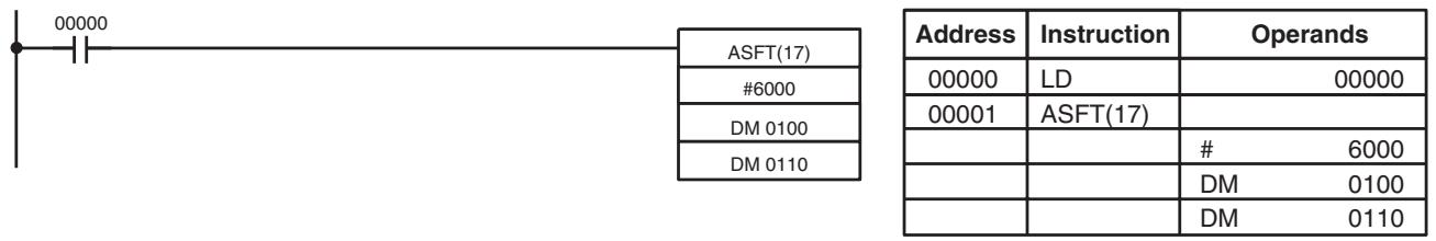
flowchart
graph LR
    A["00000"] --> B["ASFT(17)"]
    B --> C["#6000"]
    C --> D["DM 0100"]
    D --> E["DM 0110"]
    F["Address"] --> G["Instruction"] --> H["Operands"]
    I["00000"] --> J["LD"] --> K["00000"]
    L["00001"] --> M["ASFT(17)"] --> N["# 6000"]
    O["DM"] --> P["DM 0100"]
    Q["DM"] --> R["DM 0110"]
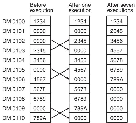
bar_stacked
| | Before execution | After one execution | After seven executions | | ------ | ---------------- | ------------------- | --------------------- | | DM 0100 | 1234 | 1234 | 1234 | | DM 0101 | 0000 | 0000 | 2345 | | DM 0102 | 0000 | 2345 | 3456 | | DM 0103 | 2345 | 0000 | 4567 | | DM 0104 | 3456 | 3456 | 5678 | | DM 0105 | 0000 | 4567 | 6789 | | DM 0106 | 4567 | 0000 | 789A | | DM 0107 | 5678 | 5678 | 0000 | | DM 0108 | 6789 | 6789 | 0000 | | DM 0109 | 0000 | 789A | 0000 | | DM 0110 | 789A | 0000 | 0000 |Note The zeroes are shifted “upward” if C=4000, and the entire shift register is set to zero if C=8000.
5-18 Data Movement Instructions
5-18-1 MOVE - MOV(21)
Ladder Symbols
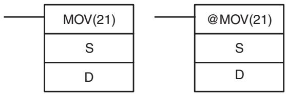
flowchart
graph TD
    A["MOV(21)"] --> B["S"]
    A --> C["D"]
    D["@MOV(21)"] --> E["S"]
    D --> F["D"]
Operand Data Areas
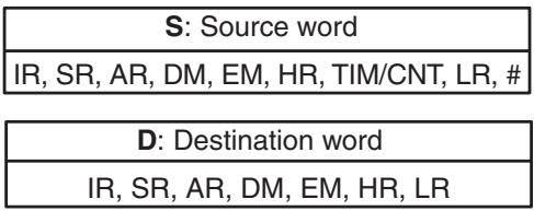
Limitations
DM 6144 to DM 6655 cannot be used for D.
Description
When the execution condition is OFF, MOV(21) is not executed. When the execution condition is ON, MOV(21) copies the content of S to D.
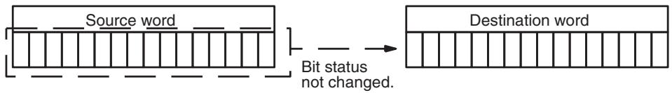
flowchart
graph LR
    A["Source word"] --> B["Bit status not changed"]
    B --> C["Destination word"]
Precautions
TIM/CNT numbers cannot be designated as D to change the PV of the timer or counter. You can, however, easily change the PV of a timer or a counter by using BSET(71).
Flags
ER: Indirectly addressed EM/DM word is non-existent.
(Content of *EM/*DM word is not BCD, or the EM/DM area boundary has been exceeded.)
EQ: ON when all zeros are transferred to D.
Example
The following example shows @MOV(21) being used to copy the content of IR 001 to HR 05 when IR 00000 goes from OFF to ON.
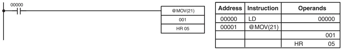
flowchart
graph LR
    A["00000"] --> B["@MOV(21)"]
    B --> C["001"]
    B --> D["HR 05"]
    E["Address"] --> F["Instruction"] --> G["Operands"]
    H["00000"] --> I["LD"] --> J["00000"]
    K["00001"] --> L["@MOV(21)"] --> M["001"]
    N[" "] --> O[" "] --> P["HR 05"]
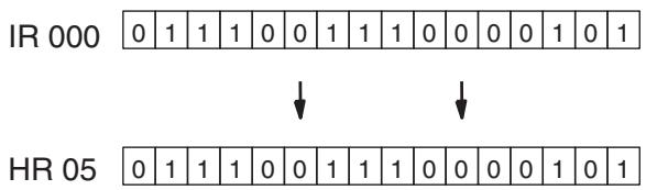
5-18-2 MOVE NOT - MVN(22)
Ladder Symbols
Operand Data Areas
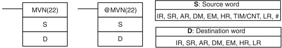
flowchart
graph TD
    A["MVN(22)"] --> B["@MVN(22)"]
    C["S"] --> B
    D["D"] --> B
    E["S"] --> B
    F["D"] --> B
    G["S: Source word"] --> H["IR, SR, AR, DM, EM, HR, TIM/CNT, LR, #"]
    I["D: Destination word"] --> J["IR, SR, AR, DM, EM, HR, LR"]
Limitations
DM 6144 to DM 6655 cannot be used for D.
Description
When the execution condition is OFF, MVN(22) is not executed. When the execution condition is ON, MVN(22) transfers the inverted content of S (specified word or four-digit hexadecimal constant) to D, i.e., for each ON bit in S, the corresponding bit in D is turned OFF, and for each OFF bit in S, the corresponding bit in D is turned ON.
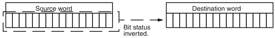
flowchart
graph LR
    A["Source word"] --> B["Bit status inverted."]
    B --> C["Destination word"]
Precautions
TIM/CNT numbers cannot be designated as D to change the PV of the timer or counter. However, these can be easily changed using BSET(71).
Flags
ER: Indirectly addressed EM/DM word is non-existent.
(Content of *EM/*DM word is not BCD, or the EM/DM area boundary has been exceeded.)
EQ: ON when all zeros are transferred to D.
Example
The following example shows @MVN(22) being used to copy the complement of #F8C5 to DM 0010 when IR 00001 goes from OFF to ON.
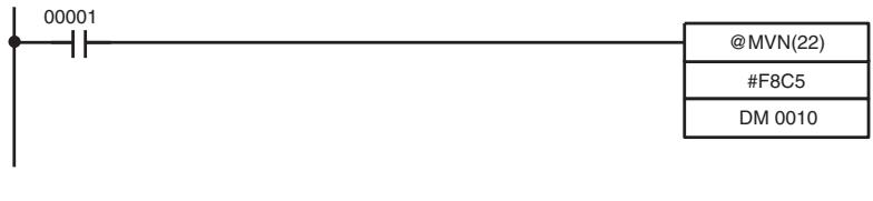
| Address | Instruction | Operands |
| 00000 | LD | 00001 |
| 00001 | @MOV(21) | |
| # F8C5 | ||
| DM 0010 |
5-18-3 BLOCK TRANSFER - XFER(70)
Operand Data Areas
| Ladder Symbols | |
| XFER(70) | @XFER(70) |
| N | N |
| S | S |
| D | D |
Limitations
S and S+N must be in the same data area, as must D and D+N.
DM 6144 to DM 6655 cannot be used for D.
Description
When the execution condition is OFF, XFER(70) is not executed. When the execution condition is ON, XFER(70) copies the contents of S, S+1, ..., S+N to D, D+1, ..., D+N.
flowchart
graph TD
    A["S\n3 4 5 2"] --> B["D\n3 4 5 2"]
    C["S+1\n3 4 5 1"] --> D["D+1\n3 4 5 1"]
    E["S+2\n3 4 2 2"] --> F["D+2\n3 4 2 2"]
    G["S+N\n6 4 5 2"] --> H["D+N\n6 4 5 2"]
    style A fill:#f9f,stroke:#333
    style C fill:#f9f,stroke:#333
    style E fill:#f9f,stroke:#333
    style G fill:#f9f,stroke:#333
    style B fill:#ccf,stroke:#333
    style D fill:#ccf,stroke:#333
    style F fill:#ccf,stroke:#333
    style H fill:#ccf,stroke:#333
Flags
ER: N is not BCD.
S and S+N or D and D+N are not in the same data area.
Indirectly addressed EM/DM word is non-existent.
(Content of *EM/*DM word is not BCD, or the EM/DM area boundary has been exceeded.)
5-18-4 BLOCK SET - BSET(71)
Operand Data Areas
| Ladder Symbols | |
| BSET(71) | @BSET(71) |
| S | S |
| St | St |
| E | E |
Limitations
St must be less than or equal to E, and St and E must be in the same data area.
DM 6144 to DM 6655 cannot be used for St or E.
Description
When the execution condition is OFF, BSET(71) is not executed. When the execution condition is ON, BSET(71) copies the content of S to all words from St through E.
flowchart
graph TD
    S[" S "] --> St[" St "]
    S --> St+1[" St+1 "]
    S --> St+2[" St+2 "]
    S --> E[" E "]
    St --> 3[" 3 4 5 2 "]
    St+1 --> 3[" 3 4 5 2 "]
    St+2 --> 3[" 3 4 5 2 "]
    E --> 3[" 3 4 5 2 "]
BSET(71) can be used to change timer/counter PV. (This cannot be done with MOV(21) or MVN(22).) BSET(71) can also be used to clear sections of a data area, i.e., the DM area, to prepare for executing other instructions. It can also be used to clear words by transferring all zeros.
Flags
ER: St and E are not in the same data area or St is greater than E.
Indirectly addressed EM/DM word is non-existent.
(Content of *EM/*DM word is not BCD, or the EM/DM area boundary has been exceeded.)
Example
The following example shows how to use BSET(71) to copy a constant (#0000) to a block of the DM area (DM 0000 to DM 0500) when IR 00000 is ON.
| Address | Instruction | Operands |
| 00000 | LD | 00000 |
| 00001 | @BSET(71) | |
| # 0000 | ||
| DM 0000 | ||
| DM 0500 |
5-18-5 DATA EXCHANGE – XCHG(73)
Ladder Symbols
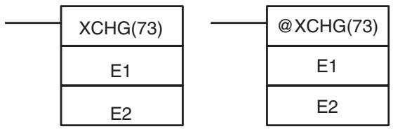
flowchart
graph LR
    A["XCHG(73)"] --> B["E1"]
    A --> C["E2"]
    D["@XCHG(73)"] --> E["E1"]
    D --> F["E2"]
Operand Data Areas
| E1: Exchange word 1 |
| IR, SR, AR, DM, EM, HR, TIM/CNT, LR |
| E2: Exchange word 2 |
| IR, SR, AR, DM, EM, HR, TIM/CNT, LR |
Limitations
DM 6144 to DM 6655 cannot be used for E1 or E2.
Description
When the execution condition is OFF, XCHG(73) is not executed. When the execution condition is ON, XCHG(73) exchanges the content of E1 and E2.
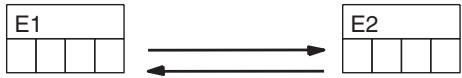
flowchart
graph LR
    E1["Block E1"] -->|双向箭头| E2["Block E2"]
If you want to exchange content of blocks whose size is greater than 1 word, use work words as an intermediate buffer to hold one of the blocks using XFER(70) three times.
Flags
ER: Indirectly addressed EM/DM word is non-existent.
(Content of *EM/*DM word is not BCD, or the EM/DM area boundary has been exceeded.)
5-18-6 SINGLE WORD DISTRIBUTE – DIST(80)
Ladder Symbols
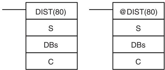
Operand Data Areas
| S: Source data |
| IR, SR, AR, DM, EM, HR, TIM/CNT, LR, # |
| DBs: Destination base word |
| IR, SR, AR, DM, EM, HR, TIM/CNT, LR |
| C: Control word (BCD) |
| IR, SR, AR, DM, EM, HR, TIM/CNT, LR, # |
Limitations
C must be BCD.
DM 6144 to DM 6655 cannot be used for DBs or C.
Description
DIST(80) can be used for single-word distribution or for a stack operation depending on the content of the control word, C.
Single-word Distribution
When bits 12 to 15 of C=0 to 8, DIST(80) can be used for a single word distribute operation. The entire contents of C specifies an offset, Of.
When the execution condition is OFF, DIST(80) is not executed. When the execution condition is ON, DIST(80) copies the content of S to DBs+Of, i.e., Of is added to DBs to determine the destination word.
Note DBs and DBs+Of must be in the same data area and cannot be between DM 6144 and DM 6655.
Example
The following example shows how to use DIST(80) to copy #00FF to HR 10 + Of. The content of LR 10 is #3005, so #00FF is copied to HR 15 (HR 10 + 5) when IR 00000 is ON.
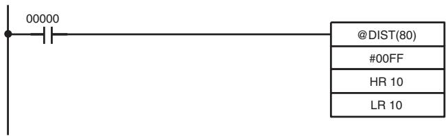
| Address | Instruction | Operands |
| 00000 | LD | 00000 |
| 00001 | @DIST(80) | |
| # 00FF | ||
| HR 10 | ||
| LR 10 |
flowchart
graph TD
    A["#00FF\n0 0 F F"] --> B["HR 10\n0 0 0 0"]
    B --> C["..."]
    C --> D["HR 15\n0 0 F F"]
Stack Operation
When bits 12 to 15 of C=9, DIST(80) can be used for a stack operation. The other 3 digits of C specify the number of words in the stack (000 to 999). The content of DBs is the stack pointer.
When the execution condition is OFF, DIST(80) is not executed. When the execution condition is ON, DIST(80) copies the content of S to DBs+1+the content of DBs. In other words, 1 and the content of DBs are added to DBs to determine the destination word. The content of DBs is then incremented by 1.
Note
- DIST(80) will be executed every cycle unless the differentiated form (@DIST(80)) is used or DIST(80) is used with DIFU(13) or DIFD(14).
- Be sure to initialize the stack pointer before using DIST(80) as a stack operation.
Example
The following example shows how to use DIST(80) to create a stack between DM 0001 and DM 0005. DM 0000 acts as the stack pointer.
| Address | Instruction | Operands |
| 00000 | LD | 00000 |
| 00001 | @DIST(80) | |
| 001 | ||
| DM 0000 | ||
| 216 |
First execution
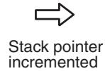

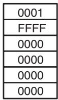
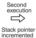
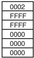
Flags
ER: The offset or stack length in the control word is not BCD.
Indirectly addressed EM/DM word is non-existent.
(Content of *EM/*DM word is not BCD, or the EM/DM area boundary has been exceeded.)
During stack operation, the value of the stack pointer+1 exceeds the length of the stack.
EQ: ON when the content of S is zero; otherwise OFF.
5-18-7 DATA COLLECT - COLL(81)
Ladder Symbols
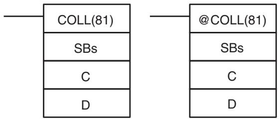
Operand Data Areas
| SBs: Source base word |
| IR, SR, AR, DM, EM, HR, TIM/CNT, LR |
| C: Control word (BCD) |
| IR, SR, AR, DM, EM, HR, TIM/CNT, LR, # |
| D: Destination word |
| IR, SR, AR, DM, EM, HR, TIM/CNT, LR |
Limitations
C must be BCD.
DM 6144 to DM 6655 cannot be used for D.
Description
COLL(81) can be used for data collection, an FIFO stack operation, or an LIFO stack operation depending on the content of the control word, C.
Data Collection
When bits 12 to 15 of C=0 to 7, COLL(81) is used for data collection. The entire contents of C specifies an offset, Of.
When the execution condition is OFF, COLL(81) is not executed. When the execution condition is ON, COLL(81) copies the content of SBs + Of to D, i.e., Of is added to SBs to determine the source word.
Note SBs and SBs+Of must be in the same data area.
Example
The following example shows how to use COLL(81) to copy the content of DM 0000+Of to IR 001. The content of 010 is #0005, so the content of DM 0005 (DM 0000 + 5) is copied to IR 001 when IR 00001 is ON.
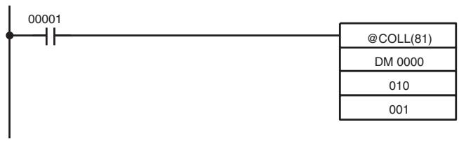
| Address | Instruction | Operands |
| 00000 | LD | 00001 |
| 00001 | @DIST(80) | |
| DM 0000 | ||
| 010 | ||
| 001 |
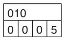
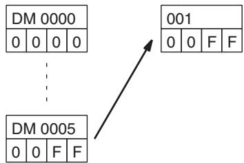
flowchart
graph TD
    A["DM 0000\n0 0 0 0"] --> D["DM 0005\n0 0 F F"]
    B["001\n0 0 F F"] --> D
FIFO Stack Operation
When bits 12 to 15 of C=9, COLL(81) can be used for an FIFO stack operation. The other 3 digits of C specify the number of words in the stack (000 to 999). The content of SBs is the stack pointer.
When the execution condition is ON, COLL(81) shifts the contents of each word within the stack down by one address, finally shifting the data from SBs+1 (the first value written to the stack) to the destination word (D). The content of the stack pointer (SBs) is then decremented by one.
Note COLL(81) will be executed every cycle unless the differentiated form (@COLL(81)) is used or COLL(81) is used with DIFU(13) or DIFD(14).
Example
The following example shows how to use COLL(81) to create a stack between DM 0001 and DM 0005. DM 0000 acts as the stack pointer.
When IR 00000 goes from OFF to ON, COLL(81) shifts the contents of DM 0002 to DM 0005 down by one address, and shifts the data from DM 0001 to IR 001. The content of the stack pointer (DM 0000) is then decremented by one.

| Address | Instruction | Operands |
| 00000 | LD | 00000 |
| 00001 | @COLL(81) | |
| DM 0000 | ||
| 216 | ||
| 001 |
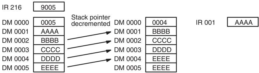
flowchart
graph TD
    A["IR 216"] --> B["9005"]
    B --> C["Stack pointer decremented"]
    C --> D["DM 0000"]
    C --> E["0004"]
    D --> F["DBBB"]
    D --> G["CCCC"]
    E --> H["DDDD"]
    E --> I["EEEE"]
    F --> J["DBBB"]
    G --> K["CCCC"]
    H --> L["DDDD"]
    I --> M["EEEE"]
    J --> N["DBBB"]
    K --> O["CCCC"]
    L --> P["DDDD"]
    M --> Q["EEEE"]
    N --> R["DBBB"]
    O --> S["CCCC"]
    P --> T["DDDD"]
    Q --> U["EEEE"]
    R --> V["DBBB"]
    S --> W["CCCC"]
    T --> X["DDDD"]
    U --> Y["EEEE"]
    V --> Z["DBBB"]
    W --> AA["CCCC"]
    X --> AB["DDDD"]
    Y --> AC["EEEE"]
    Z --> AD["DBBB"]
    AA --> AE["CCCC"]
    AB --> AF["DDDD"]
    AC --> AG["EEEE"]
    AD --> AH["DBBB"]
    AE --> AI["CCCC"]
    AF --> AJ["DDDD"]
    AG --> AK["EEEE"]
    AH --> AL["DBBB"]
    AI --> AM["CCCC"]
    AJ --> AN["DDDD"]
    AK --> AO["EEEE"]
    AL --> AP["DBBB"]
    AM --> AQ["CCCC"]
    AN --> AR["DDDD"]
    AO --> AS["EEEE"]
    AP --> AT["DBBB"]
    AQ --> AU["CCCC"]
    AR --> AV["DDDD"]
    AS --> AW["EEEE"]
    AT --> AX["DBBB"]
    AU --> AY["CCCC"]
    AV --> AZ["DDDD"]
    AW --> BA["EEEE"]
LIFO Stack Operation
When bits 12 to 15 of C=8, COLL(81) can be used for an LIFO stack operation. The other 3 digits of C specify the number of words in the stack (000 to 999). The content of SBs is the stack pointer.
When the execution condition is ON, COLL(81) copies the data from the word indicated by the stack pointer (SBs+the content of SBs) to the destination word (D). The content of the stack pointer (SBs) is then decremented by one.
The stack pointer is the only word changed in the stack.
Note COLL(81) will be executed every cycle unless the differentiated form (@DIST(80)) is used or DIST(80) is used with DIFU(13) or DIFD(14).
Example
The following example shows how to use COLL(81) to create a stack between DM 0001 and DM 0005. DM 0000 acts as the stack pointer.
When IR 00000 goes from OFF to ON, COLL(81) copies the content of DM 0005 (DM 0000 + 5) to IR 001. The content of the stack pointer (DM 0000) is then decremented by one.
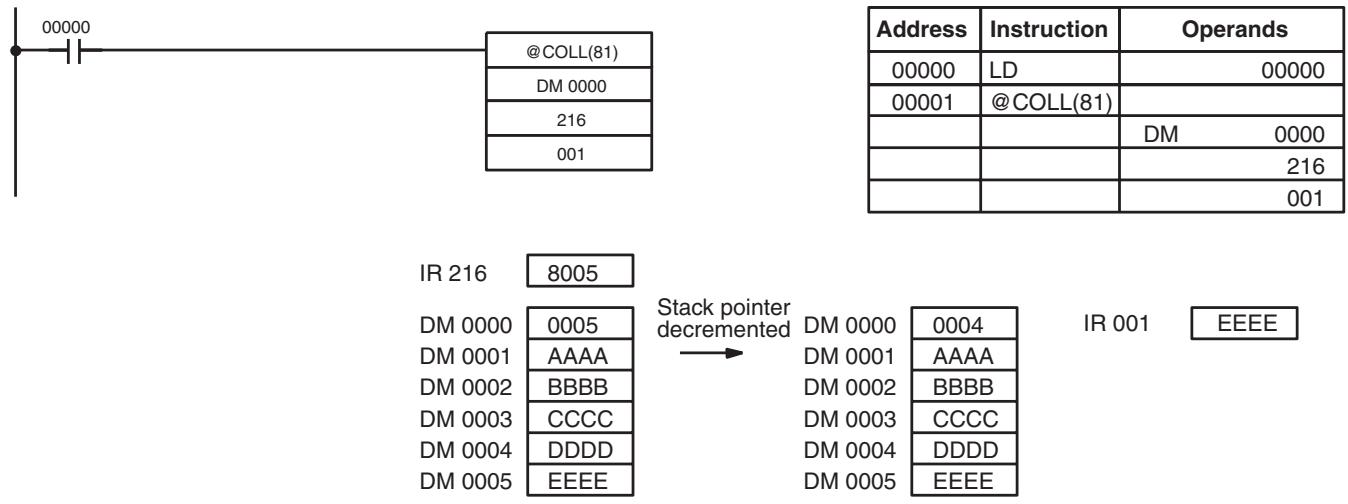
| Address | Instruction | Operands |
| 00000 | LD | 00000 |
| 00001 | @COLL(81) | |
| DM 0000 | ||
| 216 | ||
| 001 |
Flags
ER: The offset or stack length in the control word is not BCD.
Indirectly addressed EM/DM word is non-existent.
(Content of *EM/*DM word is not BCD, or the EM/DM area boundary has been exceeded.)
During stack operation, the value of the stack pointer exceeds the length of the stack; an attempt was made to write to a word beyond the end of the stack.
EQ: ON when the content of S is zero; otherwise OFF.
5-18-8 MOVE BIT - MOVB(82)
Operand Data Areas
| Ladder Symbols | |
| MOVB(82) | @MOVB(82) |
| S | S |
| Bi | Bi |
| D | D |
Limitations
The rightmost two digits and the leftmost two digits of Bi must each be between 00 and 15.
DM 6144 to DM 6655 cannot be used for Bi or D.
Description
When the execution condition is OFF, MOVB(82) is not executed. When the execution condition is ON, MOVB(82) copies the specified bit of S to the specified bit in D. The bits in S and D are specified by Bi. The rightmost two digits of Bi designate the source bit; the leftmost two bits designate the destination bit.
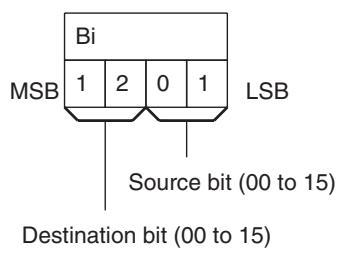
Bi
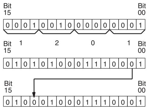
S
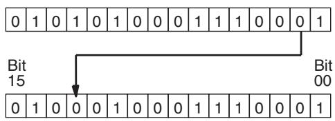
Flags
ER: Bi is not BCD, or it is specifying a non-existent bit (i.e., bit specification must be between 00 and 15).
Indirectly addressed EM/DM word is non-existent.
(Content of *EM/*DM word is not BCD, or the EM/DM area boundary has been exceeded.)
5-18-9 MOVE DIGIT – MOVD(83)
Operand Data Areas
| Ladder Symbols | |
| MOVD(83) | @MOVD(83) |
| S | S |
| Di | Di |
| D | D |
| S: Source word |
| IR, SR, AR, DM, EM, HR, TIM/CNT, LR, # |
| Di: Digit designator (BCD) |
| IR, SR, AR, DM, EM, HR, TIM/CNT, LR, # |
| D: Destination word |
| IR, SR, AR, DM, EM, HR, TIM/CNT, LR |
Limitations
The rightmost three digits of Di must each be between 0 and 3.
DM 6144 to DM 6655 cannot be used for Di or D.
Description
When the execution condition is OFF, MOVD(83) is not executed. When the execution condition is ON, MOVD(83) copies the content of the specified digit(s) in S to the specified digit(s) in D. Up to four digits can be transferred at one time. The first digit to be copied, the number of digits to be copied, and the first digit to receive the copy are designated in Di as shown below. Digits from S will be copied to consecutive digits in D starting from the designated first digit and continued for the designated number of digits. If the last digit is reached in either S or D, further digits are used starting back at digit 0.
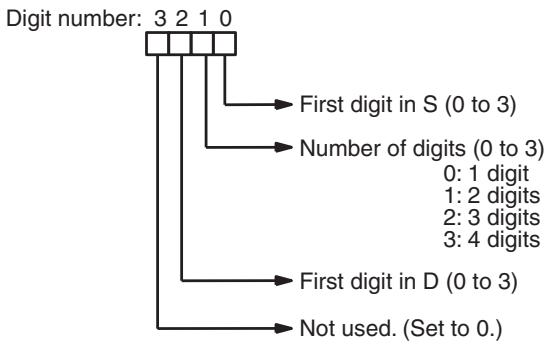
flowchart
graph TD
    A["Digit number: 3 2 1 0"] --> B["First digit in S (0 to 3)"]
    A --> C["Number of digits (0 to 3)"]
    C --> D["0: 1 digit"]
    C --> E["1: 2 digits"]
    C --> F["2: 3 digits"]
    C --> G["3: 4 digits"]
    A --> H["First digit in D (0 to 3)"]
    A --> I["Not used. (Set to 0)."]
Digit Designator
The following show examples of the data movements for various values of Di.
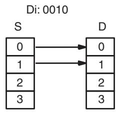
flowchart
graph LR
    S["0"] --> D["0"]
    S["1"] --> D["1"]
    S["2"] --> D["2"]
    S["3"] --> D["3"]
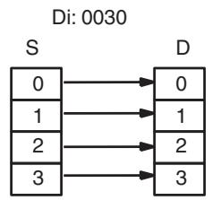
flowchart
graph LR
    S["0"] --> D["0"]
    S["1"] --> D["1"]
    S["2"] --> D["2"]
    S["3"] --> D["3"]
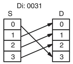
flowchart
graph TD
    S["0"] --> D["0"]
    S["1"] --> D["1"]
    S["2"] --> D["2"]
    S["3"] --> D["3"]
    D["0"] --> S["S"]
    D["1"] --> S["S"]
    D["2"] --> S["S"]
    D["3"] --> S["S"]
    S["S"] --> D["D"]
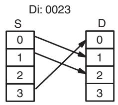
flowchart
graph TD
    S["Set S"] -->|0| D["Set D"]
    S -->|1| D
    S -->|2| D
    S -->|3| D
    D -->|0| S
    D -->|1| S
    D -->|2| S
    D -->|3| S
    style S fill:#f9f,stroke:#333
    style D fill:#f9f,stroke:#333
    note right of S Di: 0023
Flags
ER: At least one of the rightmost three digits of Di is not between 0 and 3. Indirectly addressed EM/DM word is non-existent.
(Content of *EM/*DM word is not BCD, or the EM/DM area boundary has been exceeded.)
5-18-10 TRANSFER BITS - XFRB(—)
Ladder Symbols
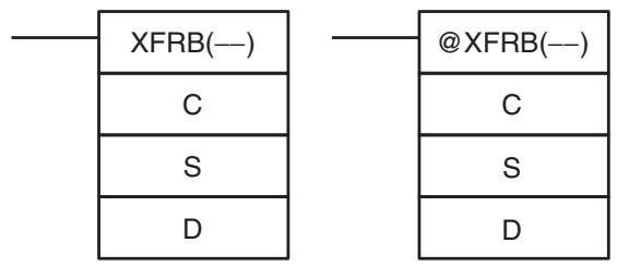
Operand Data Areas
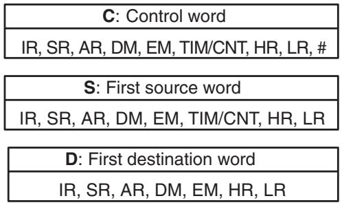
flowchart
graph TD
    A["C: Control word"] --> B["IR, SR, AR, DM, EM, TIM/CNT, HR, LR, #"]
    C["S: First source word"] --> D["IR, SR, AR, DM, EM, TIM/CNT, HR, LR"]
    E["D: First destination word"] --> F["IR, SR, AR, DM, EM, HR, LR"]
Limitations
The specified source bits must be in the same data area.
The specified destination bits must be in the same data area.
DM 6144 to DM 6655 cannot be used for D.
Description
When the execution condition is OFF, XFRB(—) is not executed. When the execution condition is ON, XFRB(—) copies the specified source bits to the specified destination bits. The two rightmost digits of C specify the starting bits in S and D and the leftmost two digits indicate the number of bits that will be copied.
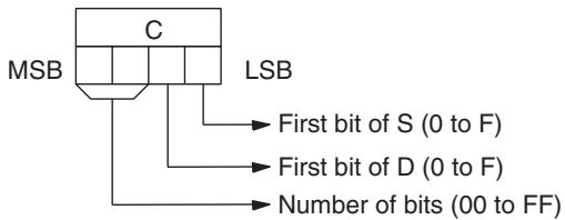
Note Up to 255 (FF) bits can be copied at one time.
Example
In the following example, XFRB(—) is used to transfer 5 bits from IR 020 and IR 021 to LR 00 and LR 01. The starting bit in IR 020 is D (13), and the starting bit in LR 00 is E (14), so IR 02013 to IR 02101 are copied to LR 0014 to LR 0102.
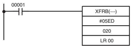
| Address | Instruction | Operands |
| 00000 | LD | 00001 |
| 00001 | XFRB(—) | |
| # 05ED | ||
| 020 | ||
| LR 00 |
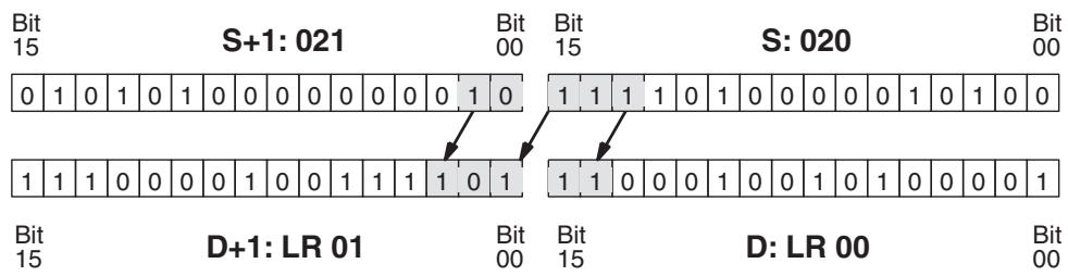
Flags
ER: The specified source bits are not all in the same data area.
The specified destination bits are not all in the same data area.
Indirectly addressed EM/DM word is non-existent.
(Content of *EM/*DM word is not BCD, or the EM/DM area boundary has been exceeded.)
5-19 Comparison Instructions
5-19-1 COMPARE - CMP(20)
Ladder Symbols
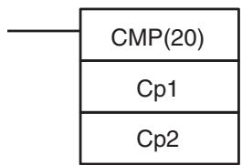
flowchart
graph TD
    A["CMP(20)"] --> B["Cp1"]
    B --> C["Cp2"]
Operand Data Areas
| Cp1: First compare word |
| IR, SR, AR, DM, EM, HR, TIM/CNT, LR, # |
Cp2: Second compare word
| IR, SR, AR, DM, EM, HR, TIM/CNT, LR, # |
Limitations
When comparing a value to the PV of a timer or counter, the value must be in BCD.
Description
When the execution condition is OFF, CMP(20) is not executed. When the execution condition is ON, CMP(20) compares Cp1 and Cp2 and outputs the result to the GR, EQ, and LE flags in the SR area.
Precautions
Placing other instructions between CMP(20) and the operation which accesses the EQ, LE, and GR flags may change the status of these flags. Be sure to access them before the desired status is changed.
Flags
ER: Indirectly addressed EM/DM word is non-existent.
(Content of *EM/*DM word is not BCD, or the EM/DM area boundary has been exceeded.)
EQ: ON if Cp1 equals Cp2.
LE: ON if Cp1 is less than Cp2.
GR: ON if Cp1 is greater than Cp2.
| Flag | Address | C1 < C2 | C1 = C2 | C1 > C2 |
| GR | 25505 | OFF | OFF | ON |
| EQ | 25506 | OFF | ON | OFF |
| LE | 25507 | ON | OFF | OFF |
Example: Saving CMP(20) Results
The following example shows how to save the comparison result immediately. If the content of HR 09 is greater than that of 010, 10200 is turned ON; if the two contents are equal, 10201 is turned ON; if content of HR 09 is less than that of 010, 10202 is turned ON. In some applications, only one of the three OUTs would be necessary, making the use of TR 0 unnecessary. With this type of programming, 10200, 10201, and 10202 are changed only when CMP(20) is executed.
flowchart
graph TD
    A["TR 0"] --> B["25505"]
    A --> C["25506"]
    A --> D["25507"]
    B --> E["10200"]
    C --> F["10201"]
    D --> G["10202"]
    H["CMP(20)"] --> I["HR 09"]
    H --> J["010"]
    K["Greater Than"] --> L["10200"]
    K --> M["10201"]
    K --> N["10202"]
    O["Equal"] --> P["10201"]
    O --> Q["10202"]
    R["Less Than"] --> S["10202"]
| Address | Instruction | Operands |
| 00000 | LD | 00000 |
| 00001 | OUT | TR 0 |
| 00002 | CMP(20) | |
| HR 09 | ||
| 010 | ||
| 00003 | AND | 25505 |
| 00004 | OUT | 10200 |
| Address | Instruction | Operands |
| 00005 | LD | TR 0 |
| 00006 | AND | 25506 |
| 00007 | OUT | 10201 |
| 00008 | LD | TR 0 |
| 00009 | AND | 25507 |
| 00010 | OUT | 10202 |
5-19-2 TABLE COMPARE - TCMP(85)
Ladder Symbols
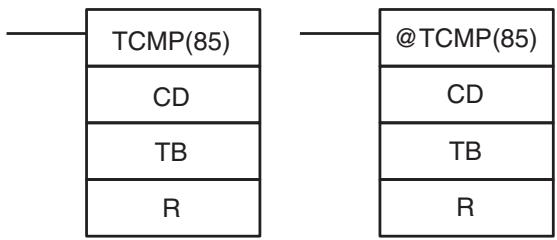
Operand Data Areas
| CD: Compare data |
| IR, SR, DM, EM, HR, TIM/CNT, LR, # |
| TB: First comparison table word |
| IR, SR, DM, EM, HR, TIM/CNT, LR |
| R: Result word |
| IR, SR, DM, EM, HR, TIM/CNT, LR |
Limitations
DM 6144 to DM 6655 cannot be used for R.
Description
When the execution condition is OFF, TCMP(85) is not executed. When the execution condition is ON, TCMP(85) compares CD to the content of TB, TB+1, TB+2, ..., and TB+15. If CD is equal to the content of any of these words, the corresponding bit in R is set, e.g., if the CD equals the content of TB, bit 00 is turned ON, if it equals that of TB+1, bit 01 is turned ON, etc. The rest of the bits in R will be turned OFF.
Flags
ER: The comparison table (i.e., TB through TB+15) exceeds the data area.
Indirectly addressed EM/DM word is non-existent.
(Content of *EM/*DM word is not BCD, or the EM/DM area boundary has been exceeded.)
Example
The following example shows the comparisons made and the results provided for TCMP(85). Here, the comparison is made during each cycle when IR 00000 is ON.
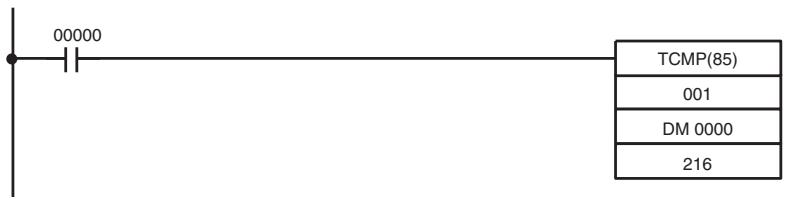
| Address | Instruction | Operands |
| 00000 | LD | 00000 |
| 00001 | TCMP(85) | |
| 001 | ||
| DM 0000 | ||
| 216 |
other
| Label | IR 001 | IR 0210 | | :--- | :--- | :--- | | DM 0000 | 0100 | IR 21600 | | IR 21600 | 0 | IR 21601 | | DM 0001 | 0200 | IR 21602 | | IR 21601 | 0 | IR 21603 | | DM 0002 | 0210 | IR 21604 | | IR 21602 | 1 | IR 21605 | | DM 0003 | 0400 | IR 21606 | | IR 21603 | 0 | IR 21607 | | DM 0004 | 0500 | IR 21608 | | IR 21604 | 0 | IR 21609 | | DM 0005 | 0600 | IR 21610 | | IR 21605 | 0 | IR 21611 | | DM 0006 | 0210 | IR 21612 | | IR 21606 | 1 | IR 21613 | | DM 0007 | 0800 | IR 21614 | | IR 21607 | 0 | IR 21615 | | DM 0008 | 0900 | IR 21615 | | IR 21608 | 0 | IR 21615 | | DM 0009 | 1000 | IR 21615 | | IR 21609 | 0 | IR 21615 | | DM 0010 | 0210 | IR 21615 | | IR 21610 | 1 | IR 21615 | | DM 0011 | 1200 | IR 21615 | | IR 21611 | 0 | IR 21615 | | DM 0012 | 1300 | IR 21615 | | IR 21612 | 0 | IR 21615 | | DM 0013 | 1400 | IR 21615 | | IR 21613 | 0 | IR 21615 | | DM 0014 | 0210 | IR 21615 | | IR 21614 | 1 | IR 21615 | | DM 0015 | 1600 | IR 21615 | Compare the data in IR 001 with the given ranges.5-19-3 BLOCK COMPARE - BCMP(68)
Ladder Symbols
| BCMP(68) |
| CD |
| CB |
| R |
Operand Data Areas
| CD: Compare data |
| IR, SR, AR, DM, EM, HR, TIM/CNT, LR, # |
| CB: First comparison block word |
| IR, SR, DM, EM, HR, TIM/CNT, LR |
| R: Result word |
| IR, SR, AR, DM, EM, HR, TIM/CNT, LR |
Limitations
Each lower limit word in the comparison block must be less than or equal to the upper limit.
DM 6144 to DM 6655 cannot be used for R.
Description
When the execution condition is OFF, BCMP(68) is not executed. When the execution condition is ON, BCMP(68) compares CD to the ranges defined by a block consisting of CB, CB+1, CB+2, ..., CB+31. Each range is defined by two words, the first one providing the lower limit and the second word providing the upper limit. If CD is found to be within any of these ranges (inclusive of the upper and lower limits), the corresponding bit in R is set. The comparisons that are made and the corresponding bit in R that is set for each true comparison are shown below. The rest of the bits in R will be turned OFF.
| CB ≤ CD ≤ CB+1 | Bit 00 |
| CB+2 ≤ CD ≤ CB+3 | Bit 01 |
| CB+4 ≤ CD ≤ CB+5 | Bit 02 |
| CB+6 ≤ CD ≤ CB+7 | Bit 03 |
| CB+8 ≤ CD ≤ CB+9 | Bit 04 |
| CB+10 ≤ CD ≤ CB+11 | Bit 05 |
| CB+12 ≤ CD ≤ CB+13 | Bit 06 |
| CB+14 ≤ CD ≤ CB+15 | Bit 07 |
| CB+16 ≤ CD ≤ CB+17 | Bit 08 |
| CB+18 ≤ CD ≤ CB+19 | Bit 09 |
| CB+20 ≤ CD ≤ CB+21 | Bit 10 |
| CB+22 ≤ CD ≤ CB+23 | Bit 11 |
| CB+24 ≤ CD ≤ CB+25 | Bit 12 |
| CB+26 ≤ CD ≤ CB+27 | Bit 13 |
| CB+28 ≤ CD ≤ CB+29 | Bit 14 |
| CB+30 ≤ CD ≤ CB+31 | Bit 15 |
Flags
ER: The comparison block (i.e., CB through CB+31) exceeds the data area.
Indirectly addressed EM/DM word is non-existent.
(Content of *EM/*DM word is not BCD, or the EM/DM area boundary has been exceeded.)
Example
The following example shows the comparisons made and the results provided for BCMP(68). Here, the comparison is made during each cycle when IR 00000 is ON.
| Address | Instruction | Operands |
| 00000 | LD | 00000 |
| 00001 | BCMP(68) | |
| 001 | ||
| DM 0010 | ||
| LR 05 |

| 001 | 0210 |
Compare data in IR 001 (which contains 0210) with the given ranges.

| DM 0010 | 0000 |
| DM 0012 | 0101 |
| DM 0014 | 0201 |
| DM 0016 | 0301 |
| DM 0018 | 0401 |
| DM 0020 | 0501 |
| DM 0022 | 0601 |
| DM 0024 | 0701 |
| DM 0026 | 0801 |
| DM 0028 | 0901 |
| DM 0030 | 1001 |
| DM 0032 | 1101 |
| DM 0034 | 1201 |
| DM 0036 | 1301 |
| DM 0038 | 1401 |
| DM 0040 | 1501 |

other
| Memory Address | Value | |---|---| | DM 0011 | 0100 | | DM 0013 | 0200 | | DM 0015 | 0300 | | DM 0017 | 0400 | | DM 0019 | 0500 | | DM 0021 | 0600 | | DM 0023 | 0700 | | DM 0025 | 0800 | | DM 0027 | 0900 | | DM 0029 | 1000 | | DM 0031 | 1100 | | DM 0033 | 1200 | | DM 0035 | 1300 | | DM 0037 | 1400 | | DM 0039 | 1500 | | DM 0041 | 1600 | → LR 0500 LR 0501 LR 0502 LR 0503 LR 0504 LR 0505 LR 0506 LR 0507 LR 0508 LR 0509 LR 0510 LR 0511 LR 0512 LR 0513 LR 0514 LR 05155-19-4 DOUBLE COMPARE – CMPL(60)
Ladder Symbols
flowchart
graph TD
    A["CMPL(60)"] --> B["Cp1"]
    A --> C["Cp2"]
    A --> D["---"]
Operand Data Areas
| Cp1: First word of first compare word pair |
| IR, SR, AR, DM, EM, HR, TIM/CNT, LR |
| Cp2: First word of second compare word pair |
| IR, SR, AR, DM, EM, HR, TIM/CNT, LR |
Limitations
Cp1 and Cp1+1 must be in the same data area.
Cp2 and Cp2+1 must be in the same data area.
Set the third operand to 000.
Description
When the execution condition is OFF, CMPL(60) is not executed. When the execution condition is ON, CMPL(60) joins the 4-digit hexadecimal content of Cp1+1 with that of Cp1, and that of Cp2+1 with that of Cp2 to create two 8-digit hexadecimal numbers, Cp+1,Cp1 and Cp2+1,Cp2. The two 8-digit numbers are then compared and the result is output to the GR, EQ, and LE flags in the SR area.
Precautions
Placing other instructions between CMPL(60) and the operation which accesses the EQ, LE, and GR flags may change the status of these flags. Be sure to access them before the desired status is changed.
Flags
ER: Indirectly addressed EM/DM word is non-existent.
(Content of *EM/*DM word is not BCD, or the EM/DM area boundary has been exceeded.)
GR: ON if Cp1+1,Cp1 is greater than Cp2+1,Cp2.
EQ: ON if Cp1+1,Cp1 equals Cp2+1,Cp2.
LE: ON if Cp1+1,Cp1 is less than Cp2+1,Cp2.
Example:
Saving CMPL(60) Results
The following example shows how to save the comparison result immediately. If the content of HR 10, HR 09 is greater than that of 011, 010, then 10000 is turned ON; if the two contents are equal, 10001 is turned ON; if content of HR 10, HR 09 is less than that of 011, 010, then 10002 is turned ON. In some applications, only one of the three OUTs would be necessary, making the use of TR 0 unnecessary. With this type of programming, 10000, 10001, and 10002 are changed only when CMPL(60) is executed.
flowchart
graph TD
    A["TR 0"] --> B["CMPL(60)"]
    B --> C["HR 09"]
    B --> D["010"]
    B --> E["---"]
    A --> F["25505"]
    F --> G["Greater Than"]
    A --> H["25506"]
    H --> I["Equal"]
    A --> J["25507"]
    J --> K["Less Than"]
    G --> L["10000"]
    I --> M["10001"]
    K --> N["10002"]
| Address | Instruction | Operands |
| 00000 | LD | 00000 |
| 00001 | OUT | TR 0 |
| 00002 | CMPL(60) | |
| HR 09 | ||
| 010 | ||
| 00003 | AND | 25505 |
| 00004 | OUT | 10000 |
| 00005 | LD | TR 0 |
| 00006 | AND | 25506 |
| 00007 | OUT | 10001 |
| 00008 | LD | TR 0 |
| 00009 | AND | 25507 |
| 00010 | OUT | 10002 |
5-19-5 MULTI-WORD COMPARE – MCMP(19)
Operand Data Areas
| MCMP(19) | @MCMP(19) |
| TB1 | TB1 |
| TB2 | TB2 |
| R | R |
| TB1: First word of table 1 |
| IR, SR, AR, DM, EM, HR, TIM/CNT, LR |
| TB2: First word of table 2 |
| IR, SR, AR, DM, EM, HR, TIM/CNT, LR |
| R: Result word |
| IR, SR, AR, DM, EM, HR, TIM/CNT, LR |
Limitations
TB1 and TB1+15 must be in the same data area.
TB2 and TB2+15 must be in the same data area.
DM 6144 to DM 6655 cannot be used for R.
Description
When the execution condition is OFF, MCMP(19) is not executed. When the execution condition is ON, MCMP(19) compares the content of TB1 to TB2, TB1+1 to TB2+1, TB1+2 to TB2+2, ..., and TB1+15 to TB2+15. If the first pair is equal, the first bit in R is turned OFF, etc., i.e., if the content of TB1 equals the content of TB2, bit 00 is turned OFF, if the content of TB1+1 equals the content of TB2+1, bit 01 is turned OFF, etc. The rest of the bits in R will be turned ON.
Flags
ER: One of the tables (i.e., TB1 through TB1+15, or TB2 through TB2+15) exceeds the data area.
Indirectly addressed EM/DM word is non-existent.
(Content of *EM/*DM word is not BCD, or the EM/DM area boundary has been exceeded.)
EQ: ON if the entire contents of both tables are equal and R=0000.
Example
The following example shows the comparisons made and the results provided for MCMP(19). Here, the comparison is made during each cycle when 00000 is ON.

flowchart
graph LR
    A["00000"] --> B["MCMP(19)"]
    B --> C["100"]
    C --> D["DM 0200"]
    D --> E["DM 0300"]
    E --> F["Address"]
    F --> G["Instruction"]
    G --> H["Operands"]
    F --> I["00000"]
    I --> J["LD"]
    J --> K["00000"]
    F --> L["00001"]
    L --> M["MCMP(19)"]
    M --> N["100"]
    N --> O["DM 0200"]
    O --> P["DM 0300"]
flowchart
graph LR
    A["IR 100"] --> B["DM 0200"]
    A --> C["DM 0201"]
    A --> D["DM 0202"]
    A --> E["DM 0203"]
    A --> F["DM 0204"]
    A --> G["DM 0205"]
    A --> H["DM 0206"]
    A --> I["DM 0207"]
    A --> J["DM 0208"]
    A --> K["DM 0209"]
    A --> L["DM 0210"]
    A --> M["DM 0211"]
    A --> N["DM 0212"]
    A --> O["DM 0213"]
    A --> P["DM 0214"]
    A --> Q["DM 0215"]
    R["TB1: IR 100"] --> B
    R --> C
    R --> D
    R --> E
    R --> F
    R --> G
    R --> H
    R --> I
    R --> J
    R --> K
    R --> L
    R --> M
    R --> N
    R --> O
    R --> P
    R --> Q
    T["TB2: DM 0200"] --> B
    T --> C
    T --> D
    T --> E
    T --> F
    T --> G
    T --> H
    T --> I
    T --> J
    T --> K
    T --> L
    T --> M
    T --> N
    T --> O
    T --> P
    T --> Q
    U["R: DM 0300"] --> B
    U --> C
    U --> D
    U --> E
    U --> F
    U --> G
    U --> H
    U --> I
    U --> J
    U --> K
    U --> L
    U --> M
    U --> N
    U --> O
    U --> P
5-19-6 SIGNED BINARY COMPARE - CPS(—)
Ladder Symbols
| CPS(—) |
| Cp1 |
| Cp2 |
| 000 |
Operand Data Areas
| Cp1: First compare word |
| IR, SR, AR, DM, EM, HR, TIM/CNT, LR, # |
| Cp2: Second compare word |
| IR, SR, AR, DM, EM, HR, TIM/CNT, LR, # |
| 000 |
| Not used. Set to 000. |
Description
When the execution condition is OFF, CPS(—) is not executed. When the execution condition is ON, CPS(—) compares the 16-bit (4-digit) signed binary contents in Cp1 and Cp2 and outputs the result to the GR, EQ, and LE flags in the SR area.
Precautions
Placing other instructions between CPS(—) and the operation which accesses the EQ, LE, and GR flags may change the status of these flags. Be sure to access them before the desired status is changed.
Flags
ER: Indirectly addressed EM/DM word is non-existent.
(Content of *EM/*DM word is not BCD, or the EM/DM area boundary has been exceeded.)
EQ: ON if Cp1 equals Cp2.
LE: ON if Cp1 is less than Cp2.
GR: ON if Cp1 is greater than Cp2.
| Comparison result | Flag status | ||
| GR (SR 25505) | EQ (SR 25506) | LE (SR 25507) | |
| Cp1 < Cp2 | 0 | 0 | 1 |
| Cp1 = Cp2 | 0 | 1 | 0 |
| Cp1 > Cp2 | 1 | 0 | 0 |
Example
In the following example, the content of 102 is greater than that of DM 0020, so 10000 is turned ON and the other bits, 10001 and 10002, are turned OFF.
flowchart
graph TD
    A["00500"] --> B["TR 0"]
    B --> C["CPS(−)"]
    C --> D["102"]
    C --> E["DM 0020"]
    C --> F["000"]
    B --> G["25505"]
    G --> H["Greater Than"]
    G --> I["25506"]
    I --> J["Equal"]
    I --> K["25507"]
    J --> L["10001"]
    K --> M["10002"]
    L --> N["10000"]
    M --> O["10002"]
| Address | Instruction | Operands |
| 00000 | LD | 00500 |
| 00001 | OUT | TR 0 |
| 00002 | CPS(—) | |
| 102 | ||
| DM 0020 | ||
| 000 | ||
| 00003 | AND | 25505 |
| 00004 | OUT | 10000 |
| 00005 | LD | TR 0 |
| 00006 | AND | 25506 |
| 00007 | OUT | 10001 |
| 00008 | LD | TR 0 |
| 00009 | AND | 25507 |
| 00010 | OUT | 10002 |
5-19-7 DOUBLE SIGNED BINARY COMPARE - CPSL(—)
Ladder Symbols
| CPSL(—) |
| Cp1 |
| Cp2 |
| 000 |
Operand Data Areas
| Cp1: First compare word |
| IR, SR, AR, DM, EM, HR, TIM/CNT, LR, # |
| Cp2: Second compare word |
| IR, SR, AR, DM, EM, HR, TIM/CNT, LR, # |
| 000 |
| Not used. Set to 000. |
Description
When the execution condition is OFF, CPSL(—) is not executed. When the execution condition is ON, CPSL(—) compares the 32-bit (8-digit) signed binary contents in Cp1+1, Cp1 and Cp2+1, Cp2 and outputs the result to the GR, EQ, and LE flags in the SR area.
Precautions
Placing other instructions between CPSL(—) and the operation which accesses the EQ, LE, and GR flags may change the status of these flags. Be sure to access them before the desired status is changed.
Flags
ER: Indirectly addressed EM/DM word is non-existent.
(Content of *EM/*DM word is not BCD, or the EM/DM area boundary has been exceeded.)
EQ: ON if Cp1+1, Cp1 equals Cp2+1, Cp2.
LE: ON if Cp1+1, Cp1 is less than Cp2+1, Cp2.
GR: ON if Cp1+1, Cp1 is greater than Cp2+1, Cp2.
| Comparison result | Flag status | ||
| GR (SR 25505) | EQ (SR 25506) | LE (SR 25507) | |
| Cp1+1, Cp1 < Cp2+1, Cp2 | 0 | 0 | 1 |
| Cp1+1, Cp1 = Cp2+1, Cp2 | 0 | 1 | 0 |
| Cp1+1, Cp1 > Cp2+1, Cp2 | 1 | 0 | 0 |
Example
In the following example, the content of 103, 102 is less than that of DM 0021, DM 0020, so 10002 is turned ON and the other bits, 10000 and 10001, are turned OFF.
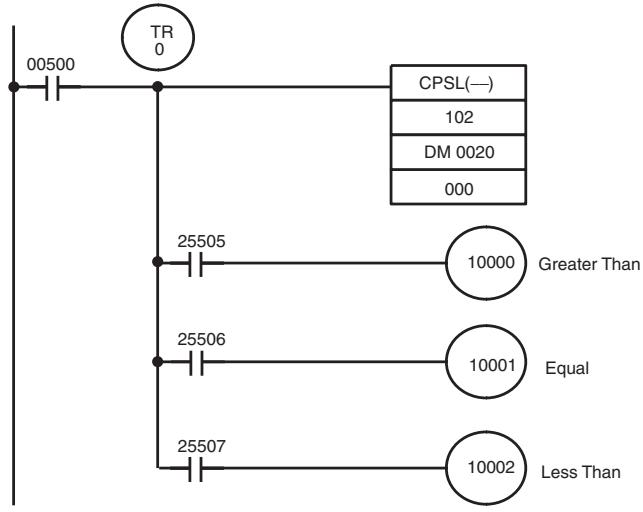
flowchart
graph TD
    A["00500"] --> B["TR 0"]
    B --> C["CPSL(—)"]
    C --> D["102"]
    C --> E["DM 0020"]
    C --> F["000"]
    B --> G["25505"]
    G --> H["Greater Than"]
    G --> I["25506"]
    I --> J["Equal"]
    I --> K["25507"]
    J --> L["10001"]
    K --> M["10002"]
| Address | Instruction | Operands |
| 00000 | LD | 00500 |
| 00001 | OUT | TR 0 |
| 00002 | CPSL(—) | |
| 102 | ||
| DM 0020 | ||
| 000 | ||
| 00003 | AND | 25505 |
| 00004 | OUT | 10000 |
| 00005 | LD | TR 0 |
| 00006 | AND | 25506 |
| 00007 | OUT | 10001 |
| 00008 | LD | TR 0 |
| 00009 | AND | 25507 |
| 00010 | OUT | 10002 |
| Cp1+1: 103 | Cp1: 102 | ||||||
| 8 | 2 | B | 6 | F | 5 | 7 | B |
(-2,101,938,823 decimal)

| Cp2+1: DM 0021 | Cp2: DM 0020 | ||||||
| 0 | 5 | 6 | A | 9 | 9 | D | B |
(90,872,283 decimal)
5-19-8 AREA RANGE COMPARE - ZCP(--)
Ladder Symbol
| ZCP(—) |
| CD |
| LL |
| UL |
Operand Data Areas
| CD: Compare data |
| IR, SR, AR, DM, EM, HR, TIM/CNT, LR, # |
| LL: Lower limit of range |
| IR, SR, AR, DM, EM, HR, TIM/CNT, LR, # |
| UL: Upper limit of range |
| IR, SR, AR, DM, EM, HR, TIM/CNT, LR, # |
Limitations
LL must be less than or equal to UL.
Description
When the execution condition is OFF, ZCP(—) is not executed. When the execution condition is ON, ZCP(—) compares CD to the range defined by lower limit LL and upper limit UL and outputs the result to the GR, EQ, and LE flags in the SR area. The resulting flag status is shown in the following table.
| Comparison result | Flag status | ||
| GR (SR 25505) | EQ (SR 25506) | LE (SR 25507) | |
| CD < LL | 0 | 0 | 1 |
| LL ≤ CD ≤ UL | 0 | 1 | 0 |
| UL < CD | 1 | 0 | 0 |
Precautions
Placing other instructions between ZCP(—) and the operation which accesses the EQ, LE, and GR flags may change the status of these flags. Be sure to access them before the desired status is changed.
Flags
ER: Indirectly addressed EM/DM word is non-existent.
(Content of *EM/*DM word is not BCD, or the EM/DM area boundary has been exceeded.)
LL is greater than UL.
EQ: ON if LL ≤ CD ≤ UL
LE: ON if CD < LL.
GR: ON if CD > UL.
Example
In the following example, the content of IR 002 (#6FA4) is compared to the range #0010 to #AB1F. Since #0010 ≤ #6FA4 ≤ #AB1F, the EQ flag and IR 10001 are turned ON.
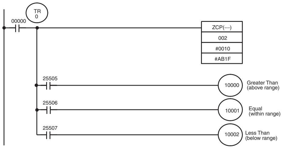
flowchart
graph TD
    A["TR 0"] --> B["ZCP(—)"]
    B --> C["002"]
    B --> D["#0010"]
    B --> E["#AB1F"]
    A --> F["25505"]
    F --> G["Greater Than (above range)"]
    A --> H["25506"]
    H --> I["Equal (within range)"]
    A --> J["25507"]
    J --> K["Less Than (below range)"]
| Address | Instruction | Operands |
| 00000 | LD | 00000 |
| 00001 | OUT | TR 0 |
| 00002 | ZCP(—) | |
| 002 | ||
| # 0010 | ||
| # AB1F | ||
| 00003 | AND | 25505 |
| Address | Instruction | Operands |
| 00004 | OUT | 10000 |
| 00005 | LD | TR 0 |
| 00006 | AND | 25506 |
| 00007 | OUT | 10001 |
| 00008 | LD | TR 0 |
| 00009 | AND | 25507 |
| 00010 | OUT | 10002 |

5-19-9 DOUBLE AREA RANGE COMPARE - ZCPL(—)
Ladder Symbol
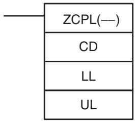
flowchart
graph TD
    A["ZCPL(—)"] --> B["CD"]
    B --> C["LL"]
    C --> D["UL"]
Operand Data Areas
| CD: Compare data |
| IR, SR, AR, DM, EM, HR, LR |
| LL: Lower limit of range |
| IR, SR, AR, DM, EM, HR, LR |
| UL: Upper limit of range |
| IR, SR, AR, DM, EM, HR, LR |
Limitations
The 8-digit value in LL+1,LL must be less than or equal to UL+1,UL.
Description
When the execution condition is OFF, ZCPL(—) is not executed. When the execution condition is ON, ZCPL(—) compares the 8-digit value in CD, CD+1 to the range defined by lower limit LL+1,LL and upper limit UL+1,UL and outputs the result to the GR, EQ, and LE flags in the SR area. The resulting flag status is shown in the following table.
| Comparison result | Flag status | ||
| GR (SR 25505) | EQ (SR 25506) | LE (SR 25507) | |
| CD, CD+1< LL+1,LL | 0 | 0 | 1 |
| LL+1,LL ≤ CD, CD+1 ≤ UL+1,UL | 0 | 1 | 0 |
| UL+1,UL < CD, CD+1 | 1 | 0 | 0 |
Precautions
Placing other instructions between ZCPL(—) and the operation which accesses the EQ, LE, and GR flags may change the status of these flags. Be sure to access them before the desired status is changed.
Flags
ER: Indirectly addressed EM/DM word is non-existent.
(Content of *EM/*DM word is not BCD, or the EM/DM area boundary has been exceeded.)
LL+1, LL is greater than UL+1, UL.
EQ: ON if LL+1,LL ≤ CD, CD+1 ≤ UL+1,UL
LE: ON if CD, CD+1 < LL+1,LL.
GR: ON if CD, CD+1 > UL+1, UL.
5-20 Conversion Instructions
5-20-1 BCD-TO-BINARY - BIN(23)
Ladder Symbols
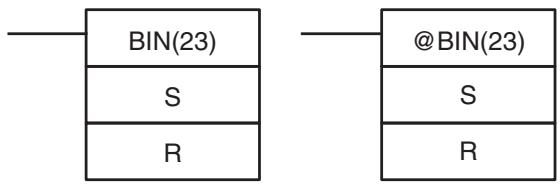
flowchart
graph TD
    A["—"] --> B["BIN(23)"]
    B --> C["S"]
    B --> D["R"]
    E["—"] --> F["@BIN(23)"]
    F --> G["S"]
    F --> H["R"]
Operand Data Areas
| S: Source word (BCD) |
| IR, SR, AR, DM, EM, HR, TIM/CNT, LR |
| R: Result word |
| IR, SR, AR, DM, EM, HR, LR |
Limitations
DM 6144 to DM 6655 cannot be used for R.
Description
When the execution condition is OFF, BIN(23) is not executed. When the execution condition is ON, BIN(23) converts the BCD content of S into the numerically equivalent binary bits, and outputs the binary value to R. Only the content of R is changed; the content of S is left unchanged.
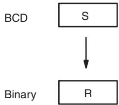
flowchart
graph TD
    A["BCD"] --> B["S"]
    B --> C["Binary"]
    C --> D["R"]
BIN(23) can be used to convert BCD to binary so that displays on the Programming Console or any other programming device will appear in hexadecimal rather than decimal. It can also be used to convert to binary to perform binary arithmetic operations rather than BCD arithmetic operations, e.g., when BCD and binary values must be added.
Flags
ER: The content of S is not BCD.
Indirectly addressed EM/DM word is non-existent.
(Content of *EM/*DM word is not BCD, or the EM/DM area boundary has been exceeded.)
EQ: ON when the result is zero.
5-20-2 BINARY-TO-BCD - BCD(24)
Ladder Symbols
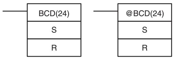
Operand Data Areas
| S: Source word (binary) |
| IR, SR, AR, DM, EM, HR, LR |
| R: Result word |
| IR, SR, AR, DM, EM, HR, LR |
Limitations
If the content of S exceeds 270F, the converted result would exceed 9999 and BCD(24) will not be executed. When the instruction is not executed, the content of R remains unchanged.
DM 6144 to DM 6655 cannot be used for R.
Description
BCD(24) converts the binary (hexadecimal) content of S into the numerically equivalent BCD bits, and outputs the BCD bits to R. Only the content of R is changed; the content of S is left unchanged.
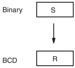
flowchart
graph TD
    A["Binary"] --> B["S"]
    B --> C["R"]
    C --> D["BCD"]
BCD(24) can be used to convert binary to BCD so that displays on the Programming Console or any other programming device will appear in decimal rather than hexadecimal. It can also be used to convert to BCD to perform BCD arithmetic operations rather than binary arithmetic operations, e.g., when BCD and binary values must be added.
Flags
ER: Indirectly addressed EM/DM word is non-existent.
(Content of *EM/*DM word is not BCD, or the EM/DM area boundary has been exceeded.)
EQ: ON when the result is zero.
5-20-3 DOUBLE BCD-TO-DOUBLE BINARY - BINL(58)
Ladder Symbols
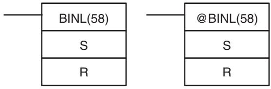
flowchart
graph TD
    A["BINL(58)"] --> B["S"]
    A --> C["R"]
    D["@BINL(58)"] --> E["S"]
    D --> F["R"]
Operand Data Areas
| S: First source word (BCD) |
| IR, SR, AR, DM, EM, HR, TIM/CNT, LR |
| R: First result word |
| IR, SR, AR, DM, EM, HR, LR |
Limitations
DM 6143 to DM 6655 cannot be used for R.
Precautions
When the execution condition is OFF, BINL(58) is not executed. When the execution condition is ON, BINL(58) converts an eight-digit number in S and S+1 into 32-bit binary data, and outputs the converted data to R and R+1.
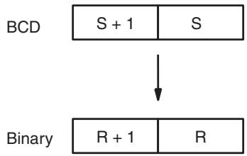
flowchart
graph TD
    A["BCD"] --> B["Binary"]
    A --> C["S + 1"] --> D["S"]
    B --> E["R + 1"] --> F["R"]
Flags
ER: The contents of S and/or S+1 words are not BCD.
Indirectly addressed EM/DM word is non-existent.
(Content of *EM/*DM word is not BCD, or the EM/DM area boundary has been exceeded.)
EQ: ON when the result is zero.
5-20-4 DOUBLE BINARY-TO-DOUBLE BCD - BCDL(59)
Ladder Symbols
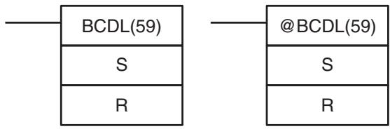
Operand Data Areas
| S: First source word (binary) |
| IR, SR, AR, DM, EM, HR, LR |
| R: First result word |
| IR, SR, AR, DM, EM, HR, LR |
Limitations
If the content of S exceeds 05F5E0FF, the converted result would exceed 99999999 and BCDL(59) will not be executed. When the instruction is not executed, the content of R and R+1 remain unchanged.
DM 6143 to DM 6655 cannot be used for R.
Description
BCDL(59) converts the 32-bit binary content of S and S+1 into eight digits of BCD data, and outputs the converted data to R and R+1.
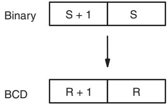
flowchart
graph TD
    A["Binary"] --> B["BCD"]
    A --> C["S + 1"] --> D["S"]
    B --> E["R + 1"] --> F["R"]
Flags
ER: Content of R and R+1 exceeds 99999999.
Indirectly addressed EM/DM word is non-existent.
(Content of *EM/*DM word is not BCD, or the EM/DM area boundary has been exceeded.)
EQ: ON when the result is zero.
5-20-5 4-TO-16 DECODER - MLPX(76)
Operand Data Areas
| Ladder Symbols | |
| MLPX(76) | @MLPX(76) |
| S | S |
| Di | Di |
| R | R |
Limitations
The rightmost two digits of Di must each be between 0 and 3.
All result words must be in the same data area.
DM 6144 to DM 6655 cannot be used for R.
Description
When the execution condition is OFF, MLPX(76) is not executed. When the execution condition is ON, MLPX(76) converts up to four, four-bit hexadecimal digits from S into decimal values from 0 to 15, each of which is used to indicate a bit position. The bit whose number corresponds to each converted value is then turned ON in a result word. If more than one digit is specified, then one bit will be turned ON in each of consecutive words beginning with R. (See examples, below.)
The following is an example of a one-digit decode operation from digit number 1 of S, i.e., here Di would be 0001.
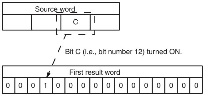
The first digit and the number of digits to be converted are designated in Di. If more digits are designated than remain in S (counting from the designated first digit), the remaining digits will be taken starting back at the beginning of S. The final word required to store the converted result (R plus the number of digits to be converted) must be in the same data area as R, e.g., if two digits are converted, the last word address in a data area cannot be designated; if three digits are converted, the last two words in a data area cannot be designated.
Digit Designator
The digits of Di are set as shown below.
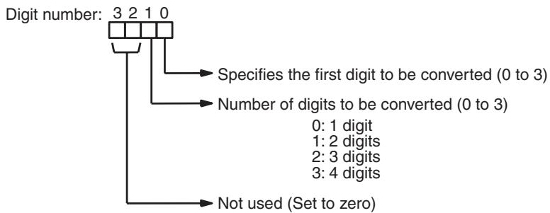
flowchart
graph TD
    A["Digit number: 3 2 1 0"] --> B["Specifies the first digit to be converted (0 to 3)"]
    A --> C["Number of digits to be converted (0 to 3)"]
    C --> D["0: 1 digit"]
    C --> E["1: 2 digits"]
    C --> F["2: 3 digits"]
    C --> G["3: 4 digits"]
    A --> H["Not used (Set to zero)"]
Some example Di values and the digit-to-word conversions that they produce are shown below.
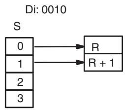
flowchart
graph LR
    S["0"] --> R["R"]
    S["0"] --> R+1["R + 1"]
    S["1"] --> R
    S["2"] --> R
    S["3"] --> R
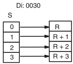
flowchart
graph LR
    S["0"] --> R["R"]
    S["0"] --> R+1["R + 1"]
    S["0"] --> R+2["R + 2"]
    S["0"] --> R+3["R + 3"]
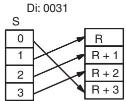
flowchart
graph TD
    S["0"] --> R["R"]
    S["0"] --> R1["R + 1"]
    S["0"] --> R2["R + 2"]
    S["0"] --> R3["R + 3"]
    S["1"] --> R["R"]
    S["1"] --> R1["R + 1"]
    S["1"] --> R2["R + 2"]
    S["1"] --> R3["R + 3"]
    S["2"] --> R["R"]
    S["2"] --> R1["R + 1"]
    S["2"] --> R2["R + 2"]
    S["2"] --> R3["R + 3"]
    S["3"] --> R["R"]
    S["3"] --> R1["R + 1"]
    S["3"] --> R2["R + 2"]
    S["3"] --> R3["R + 3"]
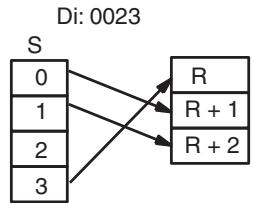
flowchart
graph TD
    S["0"] --> R["R"]
    S["0"] --> R1["R + 1"]
    S["0"] --> R2["R + 2"]
    S["0"] --> S3["3"]
    R --> S3
    R1 --> S3
    R2 --> S3
    R3 --> S3
    style S fill:#f9f,stroke:#333
    style R fill:#ccf,stroke:#333
    style R1 fill:#cfc,stroke:#333
    style R2 fill:#fcc,stroke:#333
    style R3 fill:#cff,stroke:#333
Flags
ER: Undefined digit designator, or R plus number of digits exceeds a data area.
Indirectly addressed EM/DM word is non-existent.
(Content of *EM/*DM word is not BCD, or the EM/DM area boundary has been exceeded.)
Example
The following program converts digits 1 to 3 of data from DM 0020 to bit positions and turns ON the corresponding bits in three consecutive words starting with HR 10. Digit 0 is not converted.
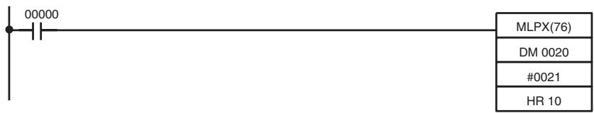
| Address | Instruction | Operands |
| 00000 | LD | 00000 |
| 00001 | MLPX(76) | |
| DM 0020 | ||
| # 0021 | ||
| HR 10 |
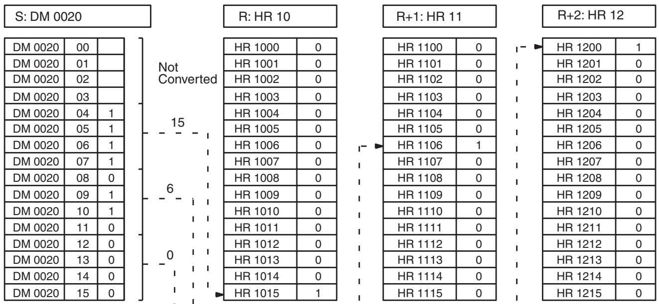
other
| S: DM 0020 | Not Converted | R: HR 10 | R+1: HR 11 | R+2: HR 12 | |---|---|---|---|---| | DM 0020 | 00 | HR 1000 | HR 1100 | HR 1200 | | DM 0020 | 01 | HR 1001 | HR 1101 | HR 1201 | | DM 0020 | 02 | HR 1002 | HR 1102 | HR 1202 | | DM 0020 | 03 | HR 1003 | HR 1103 | HR 1203 | | DM 0020 | 04 | HR 1004 | HR 1104 | HR 1204 | | DM 0020 | 05 | HR 1005 | HR 1105 | HR 1205 | | DM 0020 | 06 | HR 1006 | HR 1106 | HR 1206 | | DM 0020 | 07 | HR 1007 | HR 1107 | HR 1207 | | DM 0020 | 08 | HR 1008 | HR 1108 | HR 1208 | | DM 0020 | 09 | HR 1009 | HR 1109 | HR 1209 | | DM 0020 | 10 | HR 1010 | HR 1110 | HR 1210 | | DM 0020 | 11 | HR 1011 | HR 1111 | HR 1211 | | DM 0020 | 12 | HR 1012 | HR 1112 | HR 1212 | | DM 0020 | 13 | HR 1013 | HR 1113 | HR 1213 | | DM 0020 | 14 | HR 1014 | HR 1114 | HR 1214 | | DM 0020 | 15 | HR 1015 | HR 1115 | HR 1215 | Not Converted Not Converted HR 15 HR 6 HR 7 HR 8 HR 9 HR 10 HR 11 HR 12 HR 13 HR 14 HR 7 HR 8 HR 9 HR 15 HR 6 HR 7 HR 8 HR 9 HR 155-20-6 16-TO-4 ENCODER - DMPX(77)
Ladder Symbols
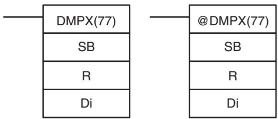
Operand Data Areas
| SB: First source word |
| IR, SR, AR, DM, EM, HR, TIM/CNT, LR |
| R: Result word |
| IR, SR, AR, DM, EM, HR, LR |
| Di: Digit designator |
| IR, SR, AR, DM, EM, HR, TIM/CNT, LR, # |
Limitations
The rightmost two digits of Di must each be between 0 and 3.
All source words must be in the same data area.
DM 6144 to DM 6655 cannot be used for SB, R, or Di.
Description
When the execution condition is OFF, DMPX(77) is not executed. When the execution condition is ON, DMPX(77) determines the position of the highest ON bit in S, encodes it into single-digit hexadecimal value corresponding to the bit number of the highest ON bit number, then transfers the hexadecimal value to the specified digit in R. The digits to receive the results are specified in Di, which also specifies the number of digits to be encoded.
The following is an example of a one-digit encode operation to digit number 1 of R, i.e., here Di would be 0001.
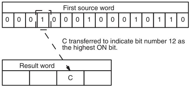
Up to four digits from four consecutive source words starting with S may be encoded and the digits written to R in order from the designated first digit. If more digits are designated than remain in R (counting from the designated first digit), the remaining digits will be placed at digits starting back at the beginning of R.
The final word to be converted (S plus the number of digits to be converted) must be in the same data area as SB.
Digit Designator
The digits of Di are set as shown below.
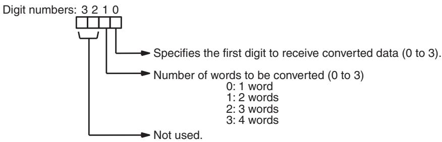
flowchart
graph TD
    A["Digit numbers: 3 2 1 0"] --> B["Specifies the first digit to receive converted data (0 to 3)."]
    A --> C["Number of words to be converted (0 to 3)"]
    C --> D["0: 1 word"]
    C --> E["1: 2 words"]
    C --> F["2: 3 words"]
    C --> G["3: 4 words"]
    A --> H["Not used."]
Some example Di values and the word-to-digit conversions that they produce are shown below.
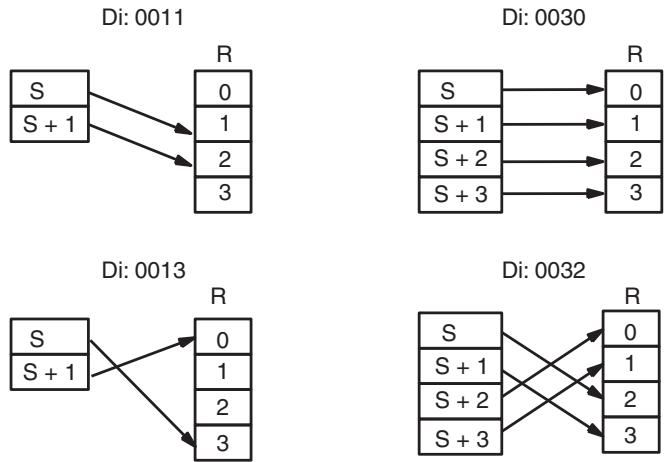
Flags
ER: Undefined digit designator, or S plus number of digits exceeds a data area.
Content of a source word is zero.
Indirectly addressed EM/DM word is non-existent.
(Content of *EM/*DM word is not BCD, or the EM/DM area boundary has been exceeded.)
Example
When 00000 is ON, the following diagram encodes IR words 010 and 011 to the first two digits of HR 10 and then encodes LR 10 and 11 to the last two digits of HR 10. Although the status of each source word bit is not shown, it is assumed that the bit with status 1 (ON) shown is the highest bit that is ON in the word.
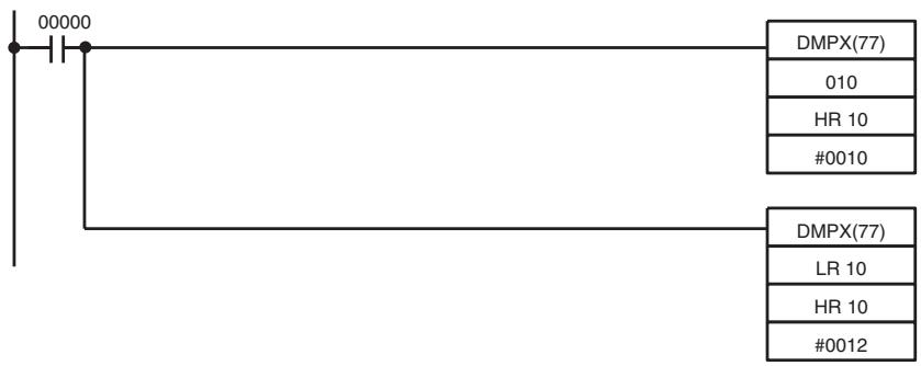
flowchart
graph TD
    A["00000"] --> B["DMPX(77)"]
    B --> C["010"]
    B --> D["HR 10"]
    B --> E["#0010"]
    A --> F["DMPX(77)"]
    F --> G["LR 10"]
    F --> H["HR 10"]
    F --> I["#0012"]
| Address | Instruction | Operands |
| 00000 | LD | 00000 |
| 00001 | DMPX(77) | |
| 010 | ||
| HR 10 | ||
| # 0010 | ||
| 00002 | DMPX(77) | |
| LR 10 | ||
| HR 10 | ||
| # 0012 |
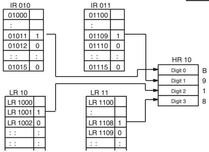
flowchart
graph TD
    subgraph IR_010
        A["IR 010"] --> B["01000"]
        A --> C["..."]
        D["IR 011"] --> E["01100"]
        D --> F["..."]
        G["IR 011"] --> H["01109"]
        G --> I["01110"]
        G --> J["..."]
        K["IR 011"] --> L["01115"]
        M["IR 011"] --> N["..."]
    end

    subgraph LR_10
        O["LR 10"] --> P["LR 1000"]
        O --> Q["LR 1001"]
        O --> R["LR 1002"]
        S["..."]
        T["..."]
    end

    subgraph LR_11
        U["LR 11"] --> V["LR 1100"]
        U --> W["..."]
        X["LR 11"] --> Y["LR 1108"]
        X --> Z["LR 1109"]
        AA["..."]
    end

    B --> R
    E --> V
    H --> W
    I --> X
    L --> Y
    P --> Z
    V --> AA
    Y --> Z
    N --> AA
    N --> AB["HR 10"]
    N --> AC["HR 10"]

    AD["HR 10"] --> AE["Digit 0"]
    AD --> AF["Digit 1"]
    AD --> AG["Digit 2"]
    AD --> AH["Digit 3"]
    AE --> AI["B"]
    AE --> AJ["B"]
    AE --> AK["B"]
    AE --> AL["B"]
    AE --> AM["B"]
    AE --> AN["B"]
5-20-7 7-SEGMENT DECODER - SDEC(78)
Ladder Symbols
| SDEC(78) | @SDEC(78) |
| S | S |
| Di | Di |
| D | D |
Operand Data Areas
| S: Source word (binary) |
| IR, SR, AR, DM, EM, HR, TIM/CNT, LR |
| Di: Digit designator |
| IR, SR, AR, DM, EM, HR, TIM/CNT, LR, # |
| D: First destination word |
| IR, SR, AR, DM, EM, HR, LR |
Limitations
Di must be within the values given below.
All destination words must be in the same data area.
DM 6144 to DM 6655 cannot be used for D.
Description
When the execution condition is OFF, SDEC(78) is not executed. When the execution condition is ON, SDEC(78) converts the designated digit(s) of S into the equivalent 8-bit, 7-segment display code and places it into the destination word(s) beginning with D.
Any or all of the digits in S may be converted in sequence from the designated first digit. The first digit, the number of digits to be converted, and the half of D to receive the first 7-segment display code (rightmost or leftmost 8 bits) are designated in Di. If multiple digits are designated, they will be placed in order starting from the designated half of D, each requiring two digits. If more digits
are designated than remain in S (counting from the designated first digit), further digits will be used starting back at the beginning of S.
Digit Designator
The digits of Di are set as shown below.
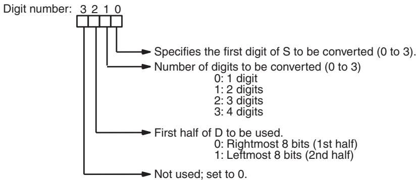
flowchart
graph TD
    A["Digit number: 3 2 1 0"] --> B["Specifies the first digit of S to be converted (0 to 3)."]
    A --> C["Number of digits to be converted (0 to 3)"]
    C --> D["0: 1 digit"]
    C --> E["1: 2 digits"]
    C --> F["2: 3 digits"]
    C --> G["3: 4 digits"]
    A --> H["First half of D to be used."]
    H --> I["0: Rightmost 8 bits (1st half)"]
    H --> J["1: Leftmost 8 bits (2nd half)"]
    A --> K["Not used; set to 0."]
Some example Di values and the 4-bit binary to 7-segment display conversions that they produce are shown below.
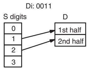
flowchart
graph TD
    A["0"] --> B["1st half"]
    C["1"] --> B
    D["2"] --> E["2nd half"]
    F["3"] --> E
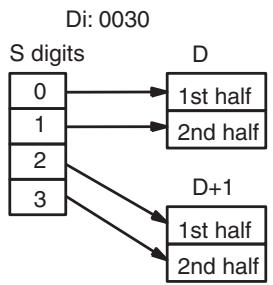
flowchart
graph TD
    A["S digits 0"] --> B["1st half"]
    C["1"] --> B
    D["2"] --> E["2nd half"]
    F["3"] --> G["D+1"]
    B --> G
    E --> G
    G --> H["1st half"]
    G --> I["2nd half"]
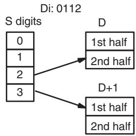
flowchart
graph TD
    A["S digits 0"] --> B["D"]
    C["0"] --> B
    D["1"] --> B
    E["2"] --> B
    F["3"] --> G["D+1"]
    H["1st half"] --> G
    I["2nd half"] --> G
    J["1st half"] --> K["D+1"]
    L["2nd half"] --> K
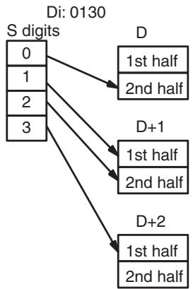
flowchart
graph TD
    A["S digits 0"] --> B["D"]
    C["0"] --> D["1st half"]
    E["1"] --> F["2nd half"]
    G["2"] --> H["D+1"]
    I["3"] --> J["1st half"]
    K["3"] --> L["2nd half"]
    M["D+2"] --> N["1st half"]
    O["D+2"] --> P["2nd half"]
Example
The following example shows the data to produce an 8. The lower case letters show which bits correspond to which segments of the 7-segment display. The table underneath shows the original data and converted code for all hexadecimal digits.
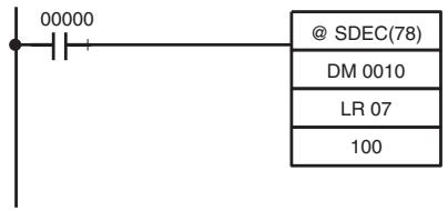
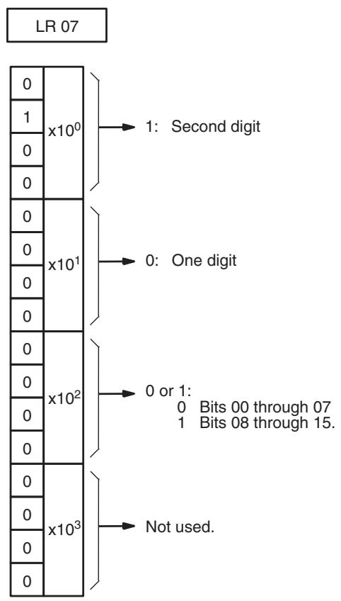
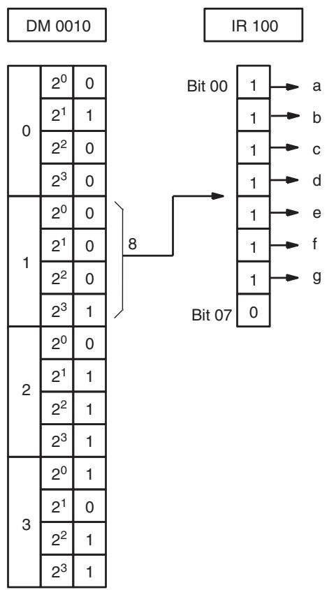
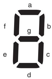
| Original data | Converted code (segments) | Display | |||||||||||
| Digit | Bits | - | g | f | e | d | c | b | a | ||||
| 0 | 0 | 0 | 0 | 0 | 0 | 0 | 1 | 1 | 0 | 0 | 0 | 0 | 0 |
| 1 | 0 | 0 | 0 | 1 | 0 | 0 | 1 | 1 | 0 | 0 | 0 | 0 | |
| 2 | 0 | 0 | 1 | 0 | 0 | 0 | 1 | 1 | 0 | 0 | 1 | 1 | 2 |
| 3 | 0 | 0 | 1 | 1 | 0 | 0 | 1 | 1 | 0 | 0 | 1 | 1 | 3 |
| 4 | 0 | 1 | 0 | 0 | 0 | 0 | 1 | 1 | 0 | 1 | 0 | 0 | 4 |
| 5 | 0 | 1 | 0 | 1 | 0 | 0 | 1 | 1 | 0 | 1 | 0 | 1 | 5 |
| 6 | 0 | 1 | 1 | 0 | 0 | 0 | 1 | 1 | 0 | 1 | 0 | 1 | 6 |
| 7 | 0 | 1 | 1 | 1 | 0 | 0 | 1 | 1 | 0 | 1 | 1 | 1 | 7 |
| 8 | 1 | 0 | 0 | 0 | 0 | 0 | 1 | 1 | 1 | 0 | 0 | 0 | 8 |
| 9 | 1 | 0 | 0 | 1 | 0 | 0 | 1 | 1 | 1 | 0 | 0 | 1 | 9 |
| A | 1 | 0 | 1 | 0 | 0 | 1 | 0 | 0 | 0 | 0 | 0 | 1 | 8 |
| B | 1 | 0 | 1 | 1 | 0 | 1 | 0 | 0 | 0 | 0 | 1 | 0 | 6 |
| C | 1 | 1 | 0 | 0 | 0 | 1 | 0 | 0 | 0 | 0 | 1 | 1 | 7 |
| D | 1 | 1 | 0 | 1 | 0 | 1 | 0 | 0 | 0 | 1 | 0 | 0 | 8 |
| E | 1 | 1 | 1 | 0 | 0 | 1 | 0 | 0 | 0 | 1 | 0 | 1 | E |
| F | 1 | 1 | 1 | 1 | 0 | 1 | 0 | 0 | 0 | 1 | 1 | 0 | F |
Flags
ER: Incorrect digit designator, or data area for destination exceeded.
Indirectly addressed EM/DM word is non-existent.
(Content of *EM/*DM word is not BCD, or the EM/DM area boundary has been exceeded.)
5-20-8 ASCII CONVERT - ASC(86)
Ladder Symbols
| ASC(86) | @ASC(86) |
| S | S |
| Di | Di |
| D | D |
Operand Data Areas
| S: Source word |
| IR, SR, AR, DM, EM, HR, TIM/CNT, LR |
| Di: Digit designator |
| IR, SR, AR, DM, EM, HR, TIM/CNT, LR, # |
| D: First destination word |
| IR, SR, AR, DM, EM, HR, LR |
Limitations
Di must be within the values given below.
All destination words must be in the same data area.
DM 6144 to DM 6655 cannot be used for D.
Description
When the execution condition is OFF, ASC(86) is not executed. When the execution condition is ON, ASC(86) converts the designated digit(s) of S into the equivalent 8-bit ASCII code and places it into the destination word(s) beginning with D.
Any or all of the digits in S may be converted in order from the designated first digit. The first digit, the number of digits to be converted, and the half of D to receive the first ASCII code (rightmost or leftmost 8 bits) are designated in Di. If multiple digits are designated, they will be placed in order starting from the designated half of D, each requiring two digits. If more digits are designated than remain in S (counting from the designated first digit), further digits will be used starting back at the beginning of S.
Note Refer to Appendix H for a table of ASCII characters.
Digit Designator
The digits of Di are set as shown below.
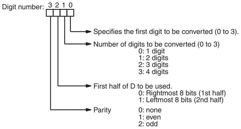
flowchart
graph TD
    A["Digit number: 3 2 1 0"] --> B["Specifies the first digit to be converted (0 to 3)."]
    A --> C["Number of digits to be converted (0 to 3)<br>0: 1 digit<br>1: 2 digits<br>2: 3 digits<br>3: 4 digits"]
    A --> D["First half of D to be used.<br>0: Rightmost 8 bits (1st half)<br>1: Leftmost 8 bits (2nd half)"]
    A --> E["Parity<br>0: none<br>1: even<br>2: odd"]
Some examples of Di values and the 4-bit binary to 8-bit ASCII conversions that they produce are shown below.
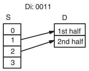
flowchart
graph TD
    S["0"] --> D["1st half"]
    S["0"] --> D["2nd half"]
    S["1"] --> D["1st half"]
    S["2"] --> D["2nd half"]
    S["3"] --> D["1st half"]
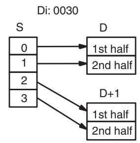
flowchart
graph TD
    S["0"] --> D1["1st half"]
    S["0"] --> D2["2nd half"]
    S["2"] --> D1["1st half"]
    S["2"] --> D2["2nd half"]
    S["3"] --> D1["1st half"]
    S["3"] --> D2["2nd half"]
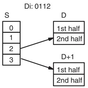
flowchart
graph TD
    S["0\n1\n2\n3"] --> D1["1st half\n2nd half"]
    S --> D2["D+1\n1st half\n2nd half"]
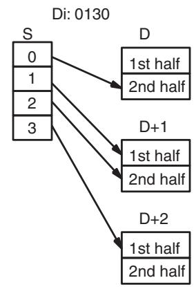
flowchart
graph TD
    S["0"] --> D1["1st half"]
    S["0"] --> D2["2nd half"]
    S["1"] --> D1["1st half"]
    S["1"] --> D2["2nd half"]
    S["2"] --> D3["1st half"]
    S["2"] --> D4["2nd half"]
    S["3"] --> D5["1st half"]
    S["3"] --> D6["2nd half"]
    D1 --> D+1["1st half"]
    D1 --> D+2["1st half"]
    D2 --> D+1["1st half"]
    D2 --> D+2["2nd half"]
    D3 --> D+2["1st half"]
    D3 --> D+3["2nd half"]
Parity
The leftmost bit of each ASCII character (2 digits) can be automatically adjusted for either even or odd parity. If no parity is designated, the leftmost bit will always be zero.
When even parity is designated, the leftmost bit will be adjusted so that the total number of ON bits is even, e.g., when adjusted for even parity, ASCII "31" (00110001) will be "B1" (10110001: parity bit turned ON to create an even number of ON bits); ASCII "36" (00110110) will be "36" (00110110: parity bit turned OFF because the number of ON bits is already even). The status of the parity bit does not affect the meaning of the ASCII code.
When odd parity is designated, the leftmost bit of each ASCII character will be adjusted so that there is an odd number of ON bits.
Flags
ER: Incorrect digit designator, or data area for destination exceeded.
Indirectly addressed EM/DM word is non-existent.
(Content of *EM/*DM word is not BCD, or the EM/DM area boundary has been exceeded.)
5-20-9 ASCII-TO-HEXADECIMAL - HEX(—)
Ladder Symbols
| S: First source word |
| IR, SR, AR, DM, EM, HR, TIM/CNT, LR, # |
| Di: Digit designator |
| IR, SR, AR, DM, EM, HR, TIM/CNT, LR, # |
| D: Destination word |
| IR, SR, AR, DM, EM, HR, LR |
Limitations
Di must be within the values given below.
All source words must be in the same data area.
Bytes in the source words must contain the ASCII code equivalent of hexadecimal values, i.e., 30 to 39 (0 to 9) or 41 to 46 (A to F).
DM 6144 to DM 6655 cannot be used for D.
Description
When the execution condition is OFF, HEX(—) is not executed. When the execution condition is ON, HEX(—) converts the designated byte(s) of ASCII code from the source word(s) into the hexadecimal equivalent and places it into D.
Up to 4 ASCII codes may be converted beginning with the designated first byte of S. The converted hexadecimal values are then placed in D in order from the designated digit. The first byte (rightmost or leftmost 8 bits), the number of bytes to be converted, and the digit of D to receive the first hexadecimal value are designated in Di. If multiple bytes are designated, they will be converted in order starting from the designated half of S and continuing to S+1 and S+2, if necessary.
If more digits are designated than remain in D (counting from the designated first digit), further digits will be used starting back at the beginning of D. Digits in D that do not receive converted data will not be changed.
Digit Designator
The digits of Di are set as shown below.
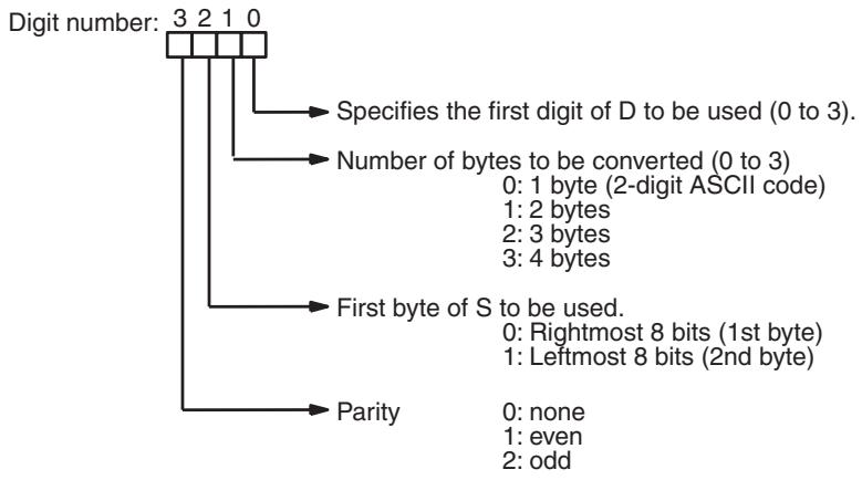
flowchart
graph TD
    A["Digit number: 3 2 1 0"] --> B["Specifies the first digit of D to be used (0 to 3)."]
    A --> C["Number of bytes to be converted (0 to 3)<br>0: 1 byte (2-digit ASCII code)<br>1: 2 bytes<br>2: 3 bytes<br>3: 4 bytes"]
    A --> D["First byte of S to be used.<br>0: Rightmost 8 bits (1st byte)<br>1: Leftmost 8 bits (2nd byte)"]
    A --> E["Parity<br>0: none<br>1: even<br>2: odd"]
Some examples of Di values and the 8-bit ASCII to 4-bit hexadecimal conversions that they produce are shown below.
ASCII Code Table
The following table shows the ASCII codes before conversion and the hexadecimal values after conversion. Refer to Appendix H for a table of ASCII characters.
| Original data | Converted data | ||||||||||||
| ASCII Code | Bit status (See note.) | Digit | Bits | ||||||||||
| 30 | * | 0 | 1 | 1 | 0 | 0 | 0 | 0 | 0 | 0 | 0 | 0 | 0 |
| 31 | * | 0 | 1 | 1 | 0 | 0 | 0 | 1 | 1 | 0 | 0 | 0 | 1 |
| 32 | * | 0 | 1 | 1 | 0 | 0 | 1 | 0 | 2 | 0 | 0 | 1 | 0 |
| 33 | * | 0 | 1 | 1 | 0 | 0 | 1 | 1 | 3 | 0 | 0 | 1 | 1 |
| 34 | * | 0 | 1 | 1 | 0 | 1 | 0 | 0 | 4 | 0 | 1 | 0 | 0 |
| 35 | * | 0 | 1 | 1 | 0 | 1 | 0 | 1 | 5 | 0 | 1 | 0 | 1 |
| 36 | * | 0 | 1 | 1 | 0 | 1 | 1 | 0 | 6 | 0 | 1 | 1 | 0 |
| 37 | * | 0 | 1 | 1 | 0 | 1 | 1 | 1 | 7 | 0 | 1 | 1 | 1 |
| 38 | * | 0 | 1 | 1 | 1 | 0 | 0 | 0 | 8 | 1 | 0 | 0 | 0 |
| 39 | * | 0 | 1 | 1 | 1 | 0 | 0 | 1 | 9 | 1 | 0 | 0 | 1 |
| 41 | * | 1 | 0 | 1 | 0 | 0 | 0 | 1 | A | 1 | 0 | 1 | 0 |
| 42 | * | 1 | 0 | 1 | 0 | 0 | 1 | 0 | B | 1 | 0 | 1 | 1 |
| 43 | * | 1 | 0 | 1 | 0 | 0 | 1 | 1 | C | 1 | 1 | 0 | 0 |
| 44 | * | 1 | 0 | 1 | 0 | 1 | 0 | 0 | D | 1 | 1 | 0 | 1 |
| 45 | * | 1 | 0 | 1 | 0 | 1 | 0 | 1 | E | 1 | 1 | 1 | 0 |
| 46 | * | 1 | 0 | 1 | 0 | 1 | 1 | 0 | F | 1 | 1 | 1 | 1 |
Note The leftmost bit of each ASCII code is adjusted for parity.
Parity
The leftmost bit of each ASCII character (2 digits) is automatically adjusted for either even or odd parity.
With no parity, the leftmost bit should always be zero. With odd or even parity, the leftmost bit of each ASCII character should be adjusted so that there is an odd or even number of ON bits.
If the parity of the ASCII code in S does not agree with the parity specified in Di, the ER Flag (SR 25503) will be turned ON and the instruction will not be executed.
Flags
ER: Incorrect digit designator, or data area for destination exceeded.
Indirectly addressed EM/DM word is non-existent.
(Content of *EM/*DM word is not BCD, or the EM/DM area boundary has been exceeded.)
Example
In the following example, the 2nd byte of LR 10 and the 1st byte of LR 11 are converted to hexadecimal values and those values are written to the first and second bytes of IR 010.
flowchart
graph TD
    A["00000"] --> B["@HEX(—)"]
    B --> C["LR 10"]
    B --> D["HR 10"]
    B --> E["010"]
    F["Address"] --> G["Instruction"]
    G --> H["Operands"]
    I["00000"] --> J["LD"]
    J --> K["00000"]
    L["00001"] --> M["@HEX(—)"]
    M --> N["LR 10"]
    M --> O["HR 10"]
    P["010"] --> Q["010"]
5-20-10 SCALING - SCL(66)
Ladder Symbols
Operand Data Areas
| S: Source word |
| IR, SR, AR, DM, EM, HR, TIM/CNT, LR, # |
| P1: First parameter word |
| IR, SR, AR, DM, EM, HR, TIM/CNT, LR |
| R: Result word |
| IR, SR, AR, DM, EM, HR, LR |
Limitations
P1 through P1+3 must be in the same data area.
DM 6144 to DM 6655 cannot be used for P1 through P1+3 or R.
Description
SCL(66) is used to linearly convert a 4-digit hexadecimal value to a 4-digit BCD value. Unlike BCD(24), which converts a 4-digit hexadecimal value to its 4-digit BCD equivalent ( S_hex S_BCD ), SCL(66) can convert the hexadecimal value according to a specified linear relationship. The conversion line is defined by two points specified in the parameter words P1 to P1+3.
When the execution condition is OFF, SCL(66) is not executed. When the execution condition is ON, SCL(66) converts the 4-digit hexadecimal value in S to the 4-digit BCD value on the line defined by points (P1, P1+1) and (P1+2, P1+3), and places the results in R. The results is rounded off to the nearest integer. If the results is less than 0000, then 0000 is written to R, and if the result is greater than 9999, then 9999 is written to R.
The following table shows the functions and ranges of the parameter words:
| Parameter | Function | Range | Comments |
| P1 | BCD point #1 ( A_Y ) | 0000 to 9999 | --- |
| P1+1 | Hex. point #1 ( A_X ) | 0000 to FFFF | Do not set P1+1=P1+3. |
| P1+2 | BCD point #2 ( B_Y ) | 0000 to 9999 | --- |
| P1+3 | Hex. point #2 ( B_X ) | 0000 to FFFF | Do not set P1+3=P1+1. |
The following diagram shows the source word, S, converted to D according to the line defined by points (A_Y, A_X) and (B_Y, B_X) .
line
| Value before conversion (Hexadecimal) | Value after conversion (BCD) | | ------------------------------------- | ---------------------------- | | A_x | A_y | | S | R | | B_x | B_y |The results can be calculated by first converting all values to BCD and then using the following formula.
$$ \text { Results } = B _ {Y} - \left[ \left(B _ {Y} - A _ {Y}\right) / \left(B _ {X} - A _ {X}\right) X \left(B _ {X} - S\right) \right] $$
Flags
ER: The value in P1+1 equals that in P1+3.
Indirectly addressed EM/DM word is non-existent.
(Content of *EM/*DM word is not BCD, or the EM/DM area boundary has been exceeded.)
P1 and P1+3 are not in the same data area, or other setting error.
EQ: ON when the result, R, is 0000.
Example
When 00000 is turned ON in the following example, the BCD source data in DM 0100 (#0100) is converted to hexadecimal according to the parameters in DM 0150 to DM 0153. The result (#0512) is then written to DM 0200.
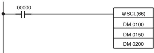
| Address | Instruction | Operands |
| 00000 | LD | 00000 |
| 00001 | @SCL(66) | |
| DM 0100 | ||
| DM 0150 | ||
| DM 0200 |
| DM 0150 | 0010 |
| DM 0151 | 0005 |
| DM 0152 | 0050 |
| DM 0153 | 0019 |
| DM 0100 | 0100 |
| DM 0200 | 0512 |
5-20-11 SIGNED BINARY TO BCD SCALING - SCL2(—)
Ladder Symbols
Operand Data Areas
| S: Source word |
| IR, SR, AR, DM, EM, HR, LR |
| P1: First parameter word |
| IR, SR, AR, DM, EM, HR, LR |
| R: Result word |
| IR, SR, AR, DM, EM, HR, LR |
Limitations
P1 through P1+2 must be in the same data area.
DM 6144 to DM 6655 cannot be used for R.
Description
SCL2(—) is used to linearly convert a 4-digit signed hexadecimal value to a 4-digit BCD value. Unlike BCD(24), which converts a 4-digit hexadecimal value to its 4-digit BCD equivalent ( S_hex S_BCD ), SCL2(—) can convert the signed hexadecimal value according to a specified linear relationship. The conversion line is defined by the x-intercept and the slope of the line specified in the parameter words P1 to P1+2.
When the execution condition is OFF, SCL2(—) is not executed. When the execution condition is ON, SCL2(—) converts the 4-digit signed hexadecimal value in S to the 4-digit BCD value on the line defined by the x-intercept (P1, 0) and the slope (P1+2 ÷ P1+1) and places the results in R. The result is rounded off to the nearest integer.
If the result is negative, then CY is set to 1. If the result is less than -9999, then -9999 is written to R. If the result is greater than 9999, then 9999 is written to R.
The following table shows the functions and ranges of the parameter words:
| Parameter | Function | Range |
| P1 | x-intercept (signed hex.) | 8000 to 7FFF (-32,768 to 32,767) |
| P1+1 | ΔX (signed hex.) | 8000 to 7FFF (-32,768 to 32,767) |
| P1+2 | ΔY (BCD) | 0000 to 9999 |
The following diagram shows the source word, S, converted to R according to the line defined by the point (P1, 0) and slope Y/ X .
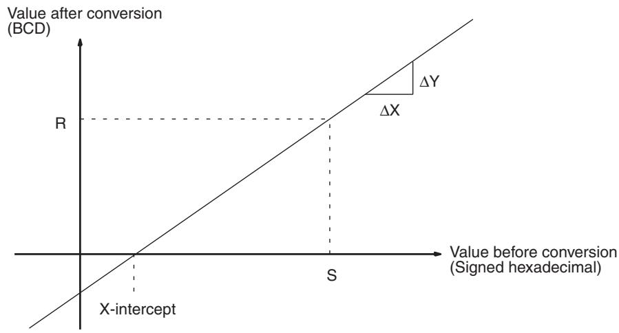
line
| Point | Value before conversion (Signed hexadecimal) | Value after conversion (BCD) | |-------|---------------------------------------------|------------------------------| | R | 0 | 0 | | S | 0 | 0 | | ΔX | 0 | 0 | | ΔY | 0 | 0 |The result can be calculated by first converting all signed hexadecimal values to BCD and then using the following formula.
$$ R = \frac {\Delta Y}{\Delta X} \times (S - P 1) $$
Flags
ER: Indirectly addressed EM/DM word is non-existent.
(Content of *EM/*DM word is not BCD, or the EM/DM area boundary has been exceeded.)
P1 and P1+2 are not in the same data area, or other setting error.
CY: ON when the result, R, is negative.
EQ: ON when the result, R, is 0000.
Example
When 05000 is turned ON in the following example, the signed binary source data in 001 (#FFE2) is converted to BCD according to the parameters in DM 0000 to DM 0002. The result (#0018) is then written to LR 00 and CY is turned ON because the result is negative.
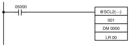
| Address | Instruction | Operands |
| 00000 | LD | 05000 |
| 00001 | @SCL2(—) | |
| 001 | ||
| DM 0000 | ||
| LR 00 |
| DM 0000 | FFFD |
| DM 0001 | 0003 |
| DM 0002 | 0002 |

line
| Point | X-axis (Left) | Y-axis (Right) | |---|---|---| | FFE2 | -0.0018 | 0 | | FFFD | 0.0000 | 1 | | 3 | 0.0018 | 2 |
flowchart
graph TD
    A["IR 001"] --> C["LR 00"]
    B["FFE2"] --> C["LR 00"]
    C["LR 00"] --> D["0018"]
    D["0018"] --> E["CY=1"]
CY flag is turned ON because the conversion result is negative.
$$ \begin{array}{l} R = \frac {0 0 0 2}{0 0 0 3} \times (F F E 2 - F F F D) \ = \frac {2}{3} \times (- 1 B) = - 1 8 \ \end{array} $$
5-20-12 BCD TO SIGNED BINARY SCALING - SCL3(—)
Ladder Symbols
Operand Data Areas
| S: Source word |
| IR, SR, AR, DM, EM, HR, LR |
P1: First parameter word
| IR, SR, AR, DM, EM, HR, LR |
R: Result word
| R: Result word |
| IR, SR, AR, DM, EM, HR, LR |
Limitations
S and P1+1 must be BCD.
P1 through P1+4 must be in the same data area.
DM 6144 to DM 6655 cannot be used for R.
Description
SCL3(—) is used to linearly convert a 4-digit BCD value to 4-digit signed hexadecimal. SCL3(—) converts the BCD value according to a specified linear relationship. The conversion line is defined by the y-intercept and the slope of the line specified in the parameter words P1 to P1+2.
When the execution condition is OFF, SCL3(—) is not executed. When the execution condition is ON, SCL3(—) converts the 4-digit BCD value in S to the 4-digit signed hexadecimal value on the line defined by the y-intercept (0, P1) and the slope (P1+2 ÷ P1+1) and places the result in R. The result is rounded off to the nearest integer.
The content of S can be 0000 to 9999, but S will be treated as a negative value if CY=1, so the effective range of S is actually -9999 to 9999. Be sure to set the desired sign in CY using STC(40) or CLC(41).
Parameter words P1+3 and P1+4 define upper and lower limits for the result. If the result is greater than the upper limit in P1+3, then the upper limit is written to R. If the result is less than the lower limit in P1+4, then the lower limit is written to R.
Note The upper and lower limits for a 12-bit Analog Input Unit would be 07FF and F800.
The following table shows the functions and ranges of the parameter words:
| Parameter | Function | Range |
| P1 | x-intercept (signed hex.) | 8000 to 7FFF (-32,768 to 32,767) |
| P1+1 | ΔX (BCD) | 0001 to 9999 |
| P1+2 | ΔY (signed hex.) | 8000 to 7FFF (-32,768 to 32,767) |
| P1+3 | Upper limit (signed hex.) | 8000 to 7FFF (-32,768 to 32,767) |
| P1+4 | Lower limit (signed hex.) | 8000 to 7FFF (-32,768 to 32,767) |
Note Do not set 0000 for X (4 digits BCD) in the second word (P1+1). The contents of P1+1 is used for division and correct conversion cannot be obtained when dividing by 0000. Correct results also cannot be obtained if a hexadecimal value is used. Always use BCD data between 0001 and 9999 for P1+1.
The following diagram shows the source word, S, converted to R according to the line defined by the point (0, P1) and slope Y/ X .

line
| Value before conversion (BCD) | Value after conversion (Signed hexadecimal) | | ------------------------------ | ------------------------------------------ | | S | ΔY | | R | ΔX | | Lower limit | - |The result can be calculated by first converting all BCD values to signed binary and then using the following formula.
$$ R = \left(\frac {\Delta Y}{\Delta X} \times S\right) + P 1 $$
Flags
ER: Indirectly addressed EM/DM word is non-existent.
(Content of *EM/*DM word is not BCD, or the EM/DM area boundary has been exceeded.)
The content of S is not BCD.
CY: CY is not changed by SCL3(—). (CY shows the sign of S before execution.)
EQ: ON when the result, R, is 0000.
Example
The status of 00101 determines the sign of the BCD source word in the following example. If 00101 is ON, then the source word is negative. When 00100 is turned ON, the BCD source data in LR 02 is converted to signed binary according to the parameters in DM 0000 to DM 0004. The result is then written to DM 0100. (In the second conversion, the signed binary equivalent of -1035 is less than the lower limit specified in DM 0004, so the lower limit is written to DM 0100.)
flowchart
graph TD
    A["25313 (Always ON)"] --> B["CLC(41)"]
    C["00101"] --> D["STC(40)"]
    E["00100"] --> F["@SCL3(-)"]
    G["LR 02"] --> H["DM 0000"]
    I["DM 0100"] --> J["DM 0100"]
| Address | Instruction | Operands |
| 00000 | LD | 25313 |
| 00001 | CLC(41) | |
| 00002 | LD | 00101 |
| 00101 | STC(40) | |
| 00004 | LD | 00100 |
| 00005 | SCL3(—) | |
| LR 02 | ||
| DM 0000 | ||
| DM 0100 |
line
| Point | BCD | Signed hex. | |---|---|---| | 1 | 0005 | 6 | | 2 | 3 | 3 |S and S+1 must be within the same data area. R and R+1 must be within the same data area. S and S+1 must be BCD and must be in the proper hours/minutes/seconds format.
DM 6143 to DM 6655 cannot be used for R.
Description
SEC(—) is used to convert time notation in hours/minutes/seconds to an equivalent in just seconds.
For the source data, the seconds are designated in bits 00 through 07 and the minutes are designated in bits 08 through 15 of S. The hours are designated in S+1. The maximum is thus 9,999 hours, 59 minutes, and 59 seconds.
The result is output to R and R+1 . The maximum obtainable value is 35,999,999 seconds.
Flags
ER: S and S+1 or R and R+1 are not in the same data area.
S and/or S+1 do not contain BCD.
Number of seconds and/or minutes exceeds 59.
Indirectly addressed EM/DM word is non-existent.
(Content of *EM/*DM word is not BCD, or the EM/DM area boundary has been exceeded.)
EQ: ON when the result is zero.
Example
When 00000 is OFF (i.e., when the execution condition is ON), the following instruction would convert the hours, minutes, and seconds given in HR 12 and HR 13 to seconds and store the results in DM 0100 and DM 0101 as shown.
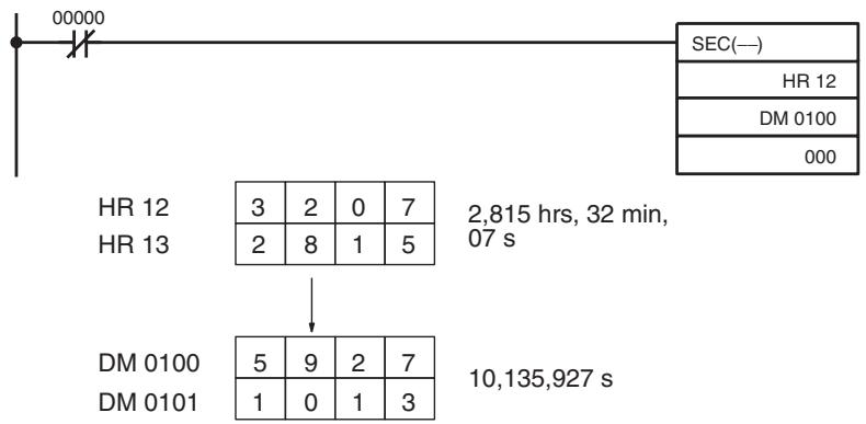
flowchart
graph TD
    A["SEC(--)"] --> B["HR 12"]
    A --> C["DM 0100"]
    A --> D["000"]
    E["HR 12"] --> F["3"]
    E --> G["2"]
    E --> H["0"]
    E --> I["7"]
    J["HR 13"] --> K["2"]
    J --> L["8"]
    J --> M["1"]
    J --> N["5"]
    O["DM 0100"] --> P["5"]
    O --> Q["9"]
    O --> R["2"]
    O --> S["7"]
    T["DM 0101"] --> U["1"]
    T --> V["0"]
    T --> W["1"]
    T --> X["3"]
    Y["2,815 hrs, 32 min, 07 s"] --> Z
    AA["10,135,927 s"] --> AB
| Address | Instruction | Operands |
| 00000 | LD NOT | 00000 |
| 00001 | SEC(—) | |
| HR 12 | ||
| DM 0100 | ||
| 000 |
5-20-14 SECONDS-TO-HOURS – HMS(—)
Ladder Symbols
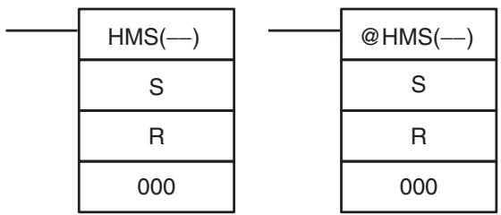
| S: Beginning source word (BCD) |
| IR, SR, AR, DM, EM, HR, TIM/CNT, LR |
| R: Beginning result word (BCD) |
| IR, SR, AR, DM, EM, HR, TIM/CNT, LR |
| 000: No function |
| 000 |
Limitations
S and S+1 must be within the same data area. R and R+1 must be within the same data area. S and S+1 must be BCD and must be between 0 and 35,999,999 seconds.
DM 6143 to DM 6655 cannot be used for R.
Description
HMS(—) is used to convert time notation in seconds to an equivalent in hours/minutes/seconds.
The number of seconds designated in S and S+1 is converted to hours/minutes/seconds and placed in R and R+1.
For the results, the seconds are placed in bits 00 through 07 and the minutes are placed in bits 08 through 15 of R. The hours are placed in R+1. The maximum is 9,999 hours, 59 minutes, and 59 seconds.
Flags
ER: S and S+1 or R and R+1 are not in the same data area.
S and/or S+1 do not contain BCD or exceed 36,000,000 seconds.
Indirectly addressed EM/DM word is non-existent.
(Content of *EM/*DM word is not BCD, or the EM/DM area boundary has been exceeded.)
EQ: ON when the result is zero.
Example
When 00000 is OFF (i.e., when the execution condition is ON), the following instruction would convert the seconds given in HR 12 and HR 13 to hours, minutes, and seconds and store the results in DM 0100 and DM 0101 as shown.
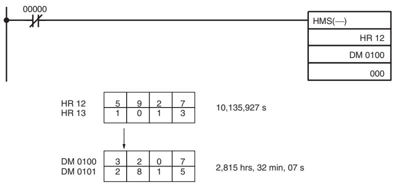
flowchart
graph TD
    A["00000"] --> B["HMS(—)"]
    B --> C["HR 12"]
    B --> D["DM 0100"]
    B --> E["000"]
    F["HR 12"] --> G["5 9 2 7"]
    F --> H["HR 13 1 0 1 3"]
    I["DM 0100"] --> J["3 2 0 7"]
    I --> K["DM 0101 2 8 1 5"]
    L["10,135,927 s"] --> M
    N["2,815 hrs, 32 min, 07 s"] --> O
| Address | Instruction | Operands |
| 00000 | LD NOT | 00000 |
| 00001 | HMS(—) | |
| HR 12 | ||
| DM 0100 | ||
| 000 |
5-20-15 COLUMN-TO-LINE - LINE(—)
Ladder Symbols
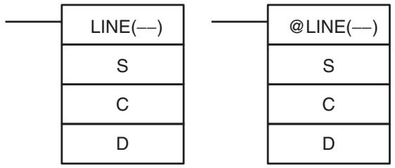
Operand Data Areas
| S: First word of 16 word source set |
| IR, SR, AR, DM, EM, HR, TIM/CNT, LR |
| C: Column bit designator (BCD) |
| IR, SR, AR, DM, EM, HR, TIM/CNT, LR, # |
| D: Destination word |
| IR, SR, AR, DM, EM, HR, TIM/CNT, LR |
Limitations
S and S+15 must be in the same data area.
C must be BCD between #0000 and #0015.
DM 6144 to DM 6655 cannot be used for D.
Description
When the execution condition is OFF, LINE(—) is not executed. When the execution condition is ON, LINE(—) copies bit column C from the 16-word set (S to S+15) to the 16 bits of word D (00 to 15).
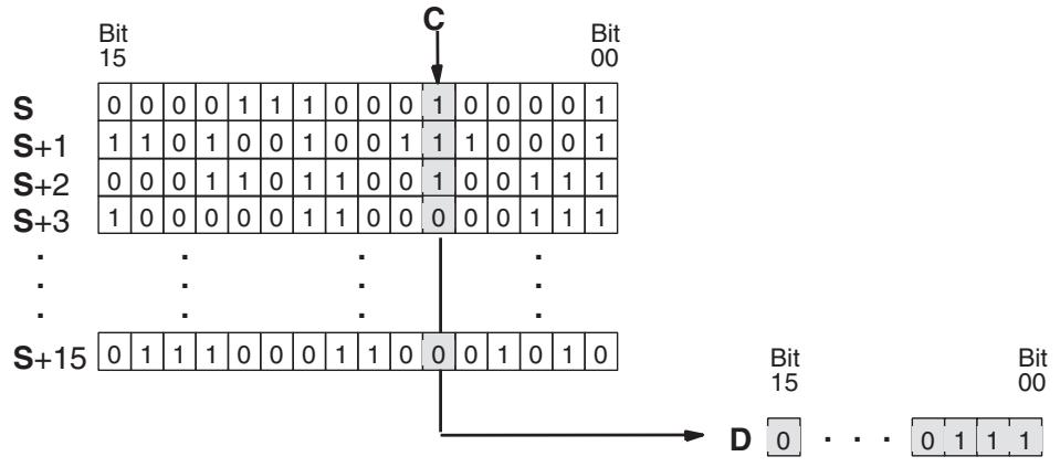
flowchart
graph TD
    A["Bit 15"] --> B["S"]
    C["Bit 00"] --> D["S+1"]
    E["S+2"] --> F["S+3"]
    G["S+15"] --> H["Bit 15"]
    I["D"] --> J["Bit 00"]
    style A fill:#f9f,stroke:#333
    style C fill:#f9f,stroke:#333
    style E fill:#f9f,stroke:#333
    style G fill:#f9f,stroke:#333
    style I fill:#f9f,stroke:#333
    style B fill:#ccf,stroke:#333
    style D fill:#ccf,stroke:#333
    style F fill:#ccf,stroke:#333
    style H fill:#ccf,stroke:#333
    style J fill:#ccf,stroke:#333
    style D fill:#ccf,stroke:#333
    style I fill:#ccf,stroke:#333
Flags
ER: The column bit designator C is not BCD, or it is specifying a non-existent bit (i.e., bit specification must be between 00 and 15).
Indirectly addressed EM/DM word is non-existent.
(Content of *EM/*DM word is not BCD, or the EM/DM area boundary has been exceeded.)
S and S+15 are not in the same data area.
EQ: ON when the content of D is zero; otherwise OFF.
Example
The following example shows how to use LINE(—) to move bit column 07 from the set (IR 100 to IR 115) to DM 0100.
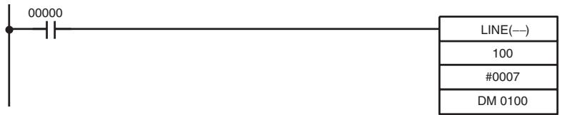
| Address | Instruction | Operands |
| 00000 | LD | 00000 |
| 00001 | LINE(---) | |
| 100 | ||
| # 0007 | ||
| DM 0100 |
5-20-16 LINE-TO-COLUMN - COLM(—)
Ladder Symbols
Operand Data Areas
| S: Source word |
| IR, SR, AR, DM, EM, HR, TIM/CNT, LR |
| D: First word of the destination set |
| IR, SR, AR, DM, EM, HR, TIM/CNT, LR |
| C: Column bit designator (BCD) |
| IR, SR, AR, DM, EM, HR, TIM/CNT, LR, # |
Limitations
D and D+15 must be in the same data area.
DM 6129 to DM 6655 cannot be used for D.
C must be BCD between #0000 and #0015.
Description
When the execution condition is OFF, COLM(—) is not executed. When the execution condition is ON, COLM(—) copies the 16 bits of word S (00 to 15) to the column of bits, C, of the 16-word set (D to D+15).
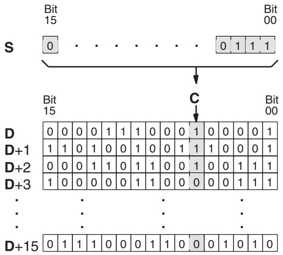
Flags
ER: The bit designator C is not BCD, or it is specifying a non-existent bit (i.e., bit specification must be between 00 and 15).
Indirectly addressed EM/DM word is non-existent.
(Content of *EM/*DM word is not BCD, or the EM/DM area boundary has been exceeded.)
D and D+15 are not in the same data area.
EQ: ON when the content of S is zero; otherwise OFF.
Example
The following example shows how to use COLM(—) to move the contents of word DM 0100 (00 to 15) to bit column 15 of the set (DM 0200 to DM 0215).
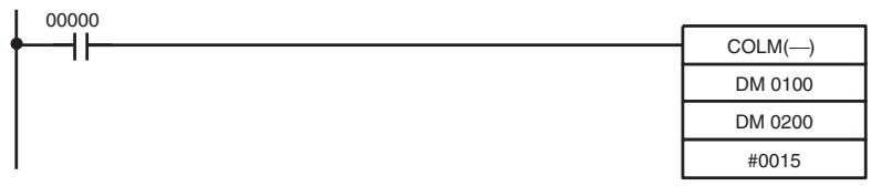
| Address | Instruction | Operands |
| 00000 | LD | 00000 |
| 00001 | COLM(—) | |
| DM 0100 | ||
| DM 0200 | ||
| # 0015 |
5-20-17 2'S COMPLEMENT – NEG(—)
Ladder Symbols
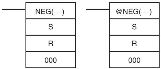
flowchart
graph TD
    A["NEG(--)"] --> B["S"]
    A --> C["R"]
    A --> D["000"]
    E["@NEG(--)"] --> F["S"]
    E --> G["R"]
    E --> H["000"]
Operand Data Areas
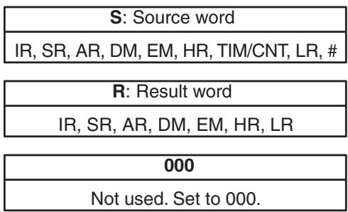
Limitations
DM 6144 to DM 6655 cannot be used for R.
Description
Converts the four-digit hexadecimal content of the source word (S) to its 2's complement and outputs the result to the result word (R). This operation is effectively the same as subtracting S from 0000 and outputting the result to R; it will calculate the absolute value of negative signed binary data.
If the content of S is 0000, the content of R will also be 0000 after execution and EQ (SR 25506) will be turned on.
If the content of S is 8000, the content of R will also be 8000 after execution and UF (SR 25405) will be turned on.
Note Refer to 1-7 Calculating with Signed Binary Data for more details.
Flags
ER: Indirectly addressed EM/DM word is non-existent.
(Content of *EM/*DM word is not BCD, or the EM/DM area boundary has been exceeded.)
EQ: ON when the content of R is zero after execution; otherwise OFF.
UF: ON when the content of S is 8000; otherwise OFF.
Example
The following example shows how to use NEG(—) to find the 2's complement of the content of DM 0005 and output the result to IR 105.

| Address | Instruction | Operands |
| 00000 | LD | 00100 |
| 00001 | NEG(—) | |
| DM 0005 | ||
| 105 | ||
| 000 |
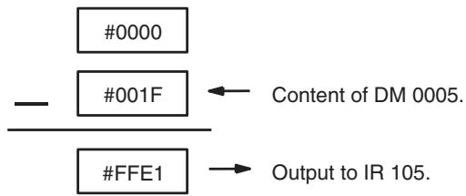
flowchart
graph TD
    A["#0000"] --> B["#001F"]
    B --> C["Content of DM 0005."]
    D["#FFE1"] --> E["Output to IR 105."]
5-20-18 DOUBLE 2'S COMPLEMENT – NEGL(—)
Ladder Symbols
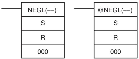
Operand Data Areas
| S: First source word |
| IR, SR, AR, DM, EM, HR, TIM/CNT, LR |
| R: First result word |
| IR, SR, AR, DM, EM, HR, LR |
| 000 |
| Not used. Set to 000. |
Limitations
DM 6143 to DM 6655 cannot be used for R.
S and S+1 must be in the same data area, as must R and R+1.
Description
Converts the eight-digit hexadecimal content of the source words (S and S+1) to its 2's complement and outputs the result to the result words (R and R+1). This operation is effectively the same as subtracting the eight-digit content S and S+1 from \$0000 0000 and outputting the result to R and R+1; it will calculate the absolute value of negative signed binary data.
If the content of S is 0000 0000, the content of R will also be 0000 0000 after execution and EQ (SR 25506) will be turned on.
If the content of S is 8000 0000, the content of R will also be 8000 0000 after execution and UF (SR 25405) will be turned on.
Note Refer to 1-7 Calculating with Signed Binary Data for more details.
Flags
ER Indirectly addressed EM/DM word is non-existent.
(Content of *EM/*DM word is not BCD, or the EM/DM area boundary has been exceeded.)
EQ: ON when the content of R+1, R is zero after execution; otherwise OFF.
UF: ON when the content of S+1, S is 8000 0000; otherwise OFF.
Example
The following example shows how to use NEGL(—) to find the 2's complement of the hexadecimal value in IR 151, IR 150 (001F FFFF) and output the result to HR 04, HR 03.
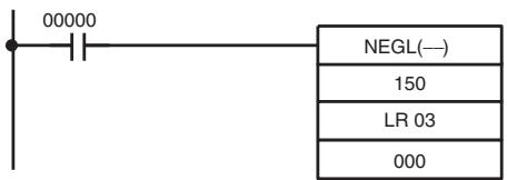
| Address | Instruction | Operands |
| 00000 | LD | 00000 |
| 00001 | NEGL(—) | |
| 150 | ||
| LR 03 | ||
| 000 |
| 0000 | 0000 |
| S+1: IR 151 | S: IR 150 |
| 001F | FFFF |
| R+1: LR 04 | R: LR 03 |
| FFE0 | 0001 |
5-21 BCD Calculation Instructions
5-21-1 SET CARRY - STC(40)
Ladder Symbols
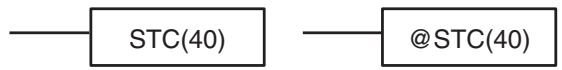
flowchart
graph LR
    A["STC(40)"] --> B["@STC(40)"]
When the execution condition is OFF, STC(40) is not executed. When the execution condition is ON, STC(40) turns ON CY (SR 25504).
Note Refer to Appendix B Error and Arithmetic Flag Operation for a table listing the instructions that affect CY.
5-21-2 CLEAR CARRY – CLC(41)
Ladder Symbols
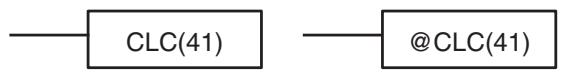
flowchart
graph LR
    A["CLC(41)"] --> B["@CLC(41)"]
When the execution condition is OFF, CLC(41) is not executed. When the execution condition is ON, CLC(41) turns OFF CY (SR 25504).
CLEAR CARRY is used to reset (turn OFF) CY (SR 25504) to "0."
Note Refer to Appendix B Error and Arithmetic Flag Operation for a table listing the instructions that affect CY.
5-21-3 BCD ADD - ADD(30)
Ladder Symbols
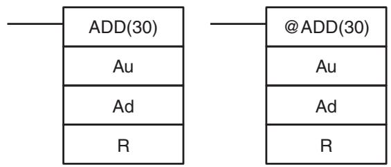
flowchart
graph TD
    A["ADD(30)"] --> B["Au"]
    A --> C["Ad"]
    A --> D["R"]
    E["@ADD(30)"] --> F["Au"]
    E --> G["Ad"]
    E --> H["R"]
Operand Data Areas
| Au: Augend word (BCD) |
| IR, SR, AR, DM, EM, HR, TIM/CNT, LR, # |
| Ad: Addend word (BCD) |
| IR, SR, AR, DM, EM, HR, TIM/CNT, LR, # |
| R: Result word |
| IR, SR, AR, DM, EM, HR, LR |
Limitations
DM 6144 to DM 6655 cannot be used for R.
Description
When the execution condition is OFF, ADD(30) is not executed. When the execution condition is ON, ADD(30) adds the contents of Au, Ad, and CY, and places the result in R. CY will be set if the result is greater than 9999.

Flags
ER: Au and/or Ad is not BCD.
Indirectly addressed EM/DM word is non-existent.
(Content of *EM/*DM word is not BCD, or the EM/DM area boundary has been exceeded.)
CY: ON when there is a carry in the result.
EQ: ON when the result is 0.
Example
If 00002 is ON, the program represented by the following diagram clears CY with CLC(41), adds the content of IR 030 to a constant (6103), places the result in DM 0100, and then moves either all zeros or 0001 into DM 0101 depending on the status of CY (25504). This ensures that any carry from the last digit is preserved in R+1 so that the entire result can be later handled as eight-digit data.
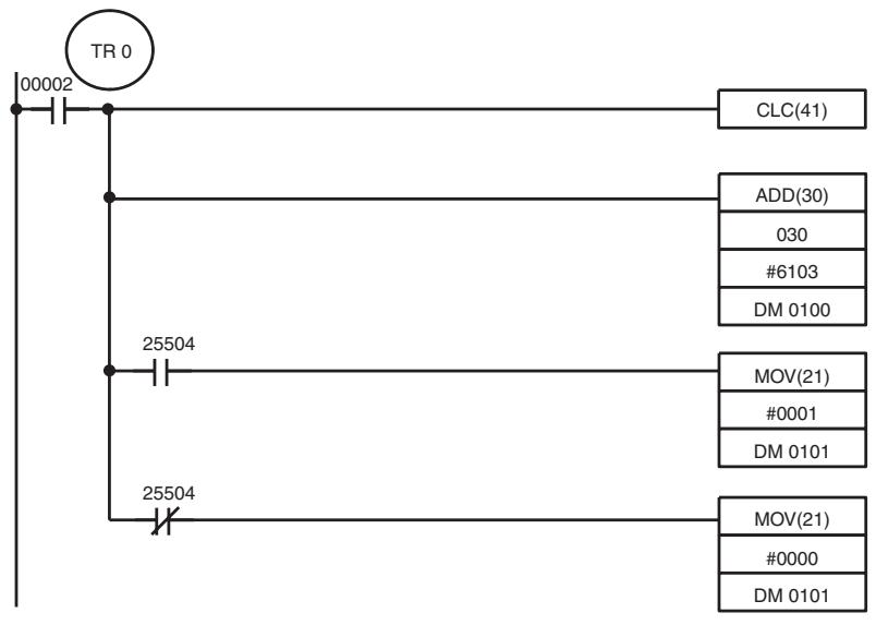
flowchart
graph TD
    A["TR 0"] --> B["00002"]
    A --> C["25504"]
    A --> D["25504"]
    C --> E["ADD(30)"]
    C --> F["#6103"]
    C --> G["DM 0100"]
    C --> H["MOV(21)"]
    C --> I["#0001"]
    C --> J["DM 0101"]
    D --> K["MOV(21)"]
    D --> L["#0000"]
    D --> M["DM 0101"]
| Address | Instruction | Operands |
| 00000 | LD | 00002 |
| 00001 | OUT | TR 0 |
| 00002 | CLC(41) | |
| 00003 | AND(30) | |
| 030 | ||
| # 6103 | ||
| DM 0100 | ||
| 00004 | AND | 25504 |
| 00005 | MOV(21) | |
| # 0001 | ||
| DM 0101 | ||
| 00006 | LD | TR 0 |
| 00007 | AND NOT | 25504 |
| 00008 | MOV(21) | |
| # 0000 | ||
| DM 0101 |
Although two ADD(30) can be used together to perform eight-digit BCD addition, ADDL(54) is designed specifically for this purpose.
5-21-4 BCD SUBTRACT – SUB(31)
Ladder Symbols
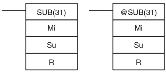
flowchart
graph TD
    A["SUB(31)"] --> B["Mi"]
    A --> C["Su"]
    A --> D["R"]
    E["@SUB(31)"] --> F["Mi"]
    E --> G["Su"]
    E --> H["R"]
Operand Data Areas
| Mi: Minuend word (BCD) |
| IR, SR, AR, DM, EM, HR, TIM/CNT, LR, # |
| Su: Subtrahend word (BCD) |
| IR, SR, AR, DM, EM, HR, TIM/CNT, LR, # |
| R: Result word |
| IR, SR, AR, DM, EM, HR, LR |
Limitations
DM 6144 to DM 6655 cannot be used for R.
Description
When the execution condition is OFF, SUB(31) is not executed. When the execution condition is ON, SUB(31) subtracts the contents of Su and CY from Mi, and places the result in R. If the result is negative, CY is set and the 10's complement of the actual result is placed in R. To convert the 10's complement to the true result, subtract the content of R from zero (see example below).

Flags
ER: Mi and/or Su is not BCD.
Indirectly addressed EM/DM word is non-existent.
(Content of *EM/*DM word is not BCD, or the EM/DM area boundary has been exceeded.)
CY: ON when the result is negative, i.e., when Mi is less than Su plus CY.
EQ: ON when the result is 0.
Caution
Be sure to clear the carry flag with CLC(41) before executing SUB(31) if its previous status is not required, and check the status of CY after doing a subtraction with SUB(31). If CY is ON as a result of executing SUB(31) (i.e., if the result is negative), the result is output as the 10's complement of the true answer. To convert the output result to the true value, subtract the value in R from 0.
Example
When 00002 is ON, the following ladder program clears CY, subtracts the contents of DM 0100 and CY from the content of 010 and places the result in HR 10.
If CY is set by executing SUB(31), the result in HR 10 is subtracted from zero (note that CLC(41) is again required to obtain an accurate result), the result is placed back in HR 10, and HR 1100 is turned ON to indicate a negative result.
If CY is not set by executing SUB(31), the result is positive, the second subtraction is not performed, and HR 1100 is not turned ON. HR 1100 is programmed as a self-maintaining bit so that a change in the status of CY will not turn it OFF when the program is rescanned.
In this example, differentiated forms of SUB(31) are used so that the subtraction operation is performed only once each time 00002 is turned ON. When another subtraction operation is to be performed, 00002 will need to be turned OFF for at least one cycle (resetting HR 1100) and then turned back ON.
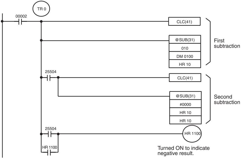
flowchart
graph TD
    A["TR 0"] --> B["00002"]
    B --> C["25504"]
    C --> D["25504"]
    D --> E["HR 1100"]
    C --> F["CLC(41)"]
    F --> G["@SUB(31)\n010\nDM 0100\nHR 10"]
    C --> H["CLC(41)"]
    H --> I["@SUB(31)\n#0000\nHR 10\nHR 10"]
    C --> J["HR 1100"]
    style A fill:#f9f,stroke:#333
    style D fill:#ccf,stroke:#333
    note right of C: First subtraction
    note right of H: Second subtraction
    note right of J: Turned ON to indicate negative result.
| Address | Instruction | Operands |
| 00000 | LD | 00002 |
| 00001 | OUT | TR 0 |
| 00002 | CLC(41) | |
| 00003 | @SUB(31) | |
| 010 | ||
| DM 0100 | ||
| HR 10 | ||
| 00004 | AND | 25504 |
| 00005 | CLC(41) | |
| 00006 | @SUB(31) | |
| # 0000 | ||
| HR 10 | ||
| HR 10 | ||
| 00007 | LD | TR 0 |
| 00008 | LD | 25504 |
| 00009 | OR | HR 1100 |
| 00010 | AND LD | |
| 00011 | OUT | HR 1100 |
The first and second subtractions for this diagram are shown below using example data for 010 and DM 0100.
Note The actual SUB(31) operation involves subtracting Su and CY from 10,000 plus Mi. For positive results the leftmost digit is truncated. For negative results the 10s complement is obtained. The procedure for establishing the correct answer is given below.
First Subtraction
| IR 010 | 1029 | |
| DM 0100 | -3452 | |
| CY | -0 | |
| HR 10 | 7577 | (1029 + (10000 - 3452)) |
| CY | 1 | (negative result) |
Second Subtraction
| 0000 | ||
| HR 10 | -7577 | |
| CY | -0 | |
| HR 10 | 2423 | (0000 + (10000 - 7577)) |
| CY 1 | (negative result) |
In the above case, the program would turn ON HR 1100 to indicate that the value held in HR 10 is negative.
5-21-5 BCD MULTIPLY - MUL(32)
Ladder Symbols
| MUL(32) | @MUL(32) |
| Md | Md |
| Mr | Mr |
| R | R |
Operand Data Areas
| Md: Multiplicand (BCD) |
| IR, SR, AR, DM, EM, HR, TIM/CNT, LR, # |
| Mr: Multiplier (BCD) |
| IR, SR, AR, DM, EM, HR, TIM/CNT, LR, # |
| R: First result word |
| IR, SR, AR, DM, EM, HR, LR |
Limitations
DM 6143 to DM 6655 cannot be used for R.
Description
When the execution condition is OFF, MUL(32) is not executed. When the execution condition is ON, MUL(32) multiplies Md by the content of Mr, and places the result In R and R+1.
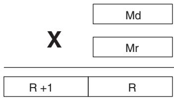
Example
When IR 00000 is ON with the following program, the contents of IR 013 and DM 0005 are multiplied and the result is placed in HR 07 and HR 08. Example data and calculations are shown below the program.
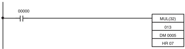
| Address | Instruction | Operands |
| 00000 | LD | 00000 |
| 00001 | MUL(32) | |
| 013 | ||
| DM 0005 | ||
| HR 07 |
| Md: IR 013 | |||
| 3 | 3 | 5 | 6 |
X
| Mr: DM 0005 | |||
| 0 | 0 | 2 | 5 |
| R+1: HR 08 | R: HR 07 | ||||||
| 0 | 0 | 0 | 8 | 3 | 9 | 0 | 0 |
Flag
ER: Md and/or Mr is not BCD.
Indirectly addressed EM/DM word is non-existent.
(Content of *EM/*DM word is not BCD, or the EM/DM area boundary has been exceeded.)
CY: ON when there is a carry in the result.
EQ: ON when the result is 0.
5-21-6 BCD DIVIDE - DIV(33)

Operand Data Areas
| Dd: Dividend word (BCD) |
| IR, SR, AR, DM, EM, HR, TIM/CNT, LR, # |
| Dr: Divisor word (BCD) |
| IR, SR, AR, DM, EM, HR, TIM/CNT, LR, # |
| R: First result word (BCD) |
| IR, SR, AR, DM, EM, HR, LR |
Limitations
R and R+1 must be in the same data area. DM 6143 to DM 6655 cannot be used for R.
Description
When the execution condition is OFF, DIV(33) is not executed and the program moves to the next instruction. When the execution condition is ON, Dd is divided by Dr and the result is placed in R and R + 1 : the quotient in R and the remainder in R + 1 .
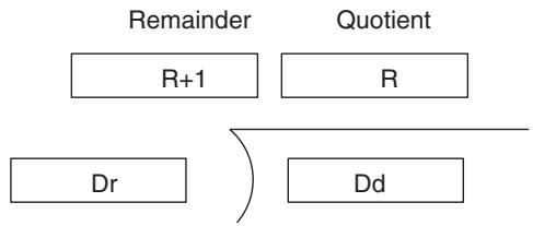
flowchart
graph TD
    A["Remainder"] --> B["R+1"]
    C["Quotient"] --> D["R"]
    E["Dr"] --> F["Dd"]
Flags
ER: Dd or Dr is not in BCD.
Indirectly addressed EM/DM word is non-existent.
(Content of *EM/*DM word is not BCD, or the EM/DM area boundary has been exceeded.)
EQ: ON when the result is 0.
Example
When IR 00000 is ON with the following program, the content of IR 216 is divided by the content of HR 09 and the result is placed in DM 0017 and DM 0018. Example data and calculations are shown below the program.

| Address | Instruction | Operands |
| 00000 | LD | 00000 |
| 00001 | DIV(33) | |
| 216 | ||
| HR 09 | ||
| DM 0017 |
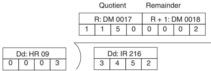
5-21-7 DOUBLE BCD ADD - ADDL(54)
Ladder Symbols

Operand Data Areas
| Au: First augend word (BCD) |
| IR, SR, AR, DM, EM, HR, TIM/CNT, LR |
| Ad: First addend word (BCD) |
| IR, SR, AR, DM, EM, HR, TIM/CNT, LR |
| R: First result word |
| IR, SR, AR, DM, EM, HR, LR |
Limitations
DM 6143 to DM 6655 cannot be used for R.
Description
When the execution condition is OFF, ADDL(54) is not executed. When the execution condition is ON, ADDL(54) adds the contents of CY to the 8-digit value in Au and Au+1 to the 8-digit value in Ad and Ad+1, and places the result in R and R+1. CY will be set if the result is greater than 99999999.
flowchart
graph TD
    A["Au + 1"] --> B["Ad + 1"]
    B --> C["CY"]
    D["R + 1"] --> E["CY"]
    F["Au"] --> G["CY"]
    H["Ad"] --> I["CY"]
    J["CY"] --> K["R"]
Flags
ER: Au and/or Ad is not BCD.
Indirectly addressed EM/DM word is non-existent.
(Content of *EM/*DM word is not BCD, or the EM/DM area boundary has been exceeded.)
CY: ON when there is a carry in the result.
EQ: ON when the result is 0.
Example
When 00000 is ON, the following program section adds two 12-digit numbers, the first contained in LR 00 through LR 02 and the second in DM 0010 through DM 0012. The result is placed in HR 10 through HR 13.
The rightmost 8 digits of the two numbers are added using ADDL(54), i.e., the contents of LR 00 and LR 01 are added to DM 0010 and DM 0011 and the results is placed in HR 10 and HR 11. The second addition adds the leftmost 4 digits of each number using ADD(30), and includes any carry from the first addition. The last instruction, ADB(50) (see 5-22-1 BINARY ADD – ADB(50)) adds two all-zero constants to place any carry from the second addition into HR 13.
flowchart
graph TD
    A["00000"] --> B["CLC(41)"]
    B --> C["@ADDL(54)"]
    C --> D["LR 00"]
    D --> E["DM 0010"]
    E --> F["HR 10"]
    F --> G["@ADD(30)"]
    G --> H["LR 02"]
    H --> I["DM 0012"]
    I --> J["HR 12"]
    J --> K["@ADB(50)"]
    K --> L["#0000"]
    L --> M["#0000"]
    M --> N["HR 13"]
    N --> O["Address Instruction Operands"]
    O --> P["00000 LD 00000"]
    O --> Q["00001 CLC(41)"]
    Q --> R["00002 @ADDL(54)"]
    R --> S["LR 00"]
    S --> T["DM 0010"]
    T --> U["HR 10"]
    U --> V["00003 @ADD(30)"]
    V --> W["LR 02"]
    W --> X["DM 0012"]
    X --> Y["HR 12"]
    Y --> Z["00004 @ADB(50)"]
    Z --> AA["# 0000"]
    AA --> AB["# 0000"]
    AB --> AC["HR 13"]
5-21-8 DOUBLE BCD SUBTRACT - SUBL(55)
Ladder Symbols
flowchart
graph TD
    A["SUBL(55)"] --> B["Mi"]
    A --> C["Su"]
    A --> D["R"]
    E["@SUBL(55)"] --> F["Mi"]
    E --> G["Su"]
    E --> H["R"]
Operand Data Areas
| Mi: First minuend word (BCD) |
| IR, SR, AR, DM, EM, HR, TIM/CNT, LR, # |
| Su: First subtrahend word (BCD) |
| IR, SR, AR, DM, EM, HR, TIM/CNT, LR, # |
| R: First result word |
| IR, SR, AR, DM, EM, HR, LR |
Limitations
DM 6143 to DM 6655 cannot be used for R.
Description
When the execution condition is OFF, SUBL(55) is not executed. When the execution condition is ON, SUBL(55) subtracts CY and the 8-digit contents of Su and Su+1 from the 8-digit value in Mi and Mi+1, and places the result in R and R+1. If the result is negative, CY is set and the 10's complement of the actual result is placed in R. To convert the 10's complement to the true result, subtract the content of R from zero. Since an 8-digit constant cannot be directly entered, use the BSET(71) instruction (see 5-18-4 BLOCK SET – BSET(71)) to create an 8-digit constant.
| Mi + 1 | Mi |
| Su + 1 | Su |
| — | CY | |
| CY | R+1 | R |
Flags
ER: Mi, M+1,Su, or Su+1 are not BCD.
Indirectly addressed EM/DM word is non-existent.
(Content of *EM/*DM word is not BCD, or the EM/DM area boundary has been exceeded.)
CY: ON when the result is negative, i.e., when Mi is less than Su.
EQ: ON when the result is 0.
Example
The following example works much like that for single-word subtraction. In this example, however, BSET(71) is required to clear the content of DM 0000 and DM 0001 so that a negative result can be subtracted from 0 (inputting an 8-digit constant is not possible).
flowchart
graph TD
    A["TR 0"] --> B["00003"]
    B --> C["25504"]
    C --> D["25504"]
    D --> E["HR 0100"]
    E --> F["HR 0100"]
    C --> G["CLC(41)"]
    C --> H["@SUBL(55)"]
    C --> I["HR 00"]
    C --> J["120"]
    C --> K["DM 0100"]
    D --> L["CLC(41)"]
    D --> M["@SUBL(55)"]
    D --> N["DM 0000"]
    D --> O["DM 0100"]
    D --> P["DM 0100"]
    style A fill:#f9f,stroke:#333
    style B fill:#ccf,stroke:#333
    style C fill:#cfc,stroke:#333
    style D fill:#fcc,stroke:#333
    style E fill:#cff,stroke:#333
    style F fill:#ffc,stroke:#333
    style G fill:#fff,stroke:#333
    style H fill:#fff,stroke:#333
    style I fill:#fff,stroke:#333
    style J fill:#fff,stroke:#333
    style K fill:#fff,stroke:#333
    style L fill:#fff,stroke:#333
    style M fill:#fff,stroke:#333
    style N fill:#fff,stroke:#333
    style O fill:#fff,stroke:#333
    style P fill:#fff,stroke:#333
| Address | Instruction | Operands |
| 00000 | LD | 00003 |
| 00001 | OUT | TR 0 |
| 00002 | CLC(41) | |
| 00003 | @SUBL(55) | |
| HR 00 | ||
| 120 | ||
| DM 0100 | ||
| 00004 | AND | 25504 |
| 00005 | @BSET(71) | |
| # 0000 | ||
| DM 0000 | ||
| DM 0001 |
| Address | Instruction | Operands |
| 00006 | CLC(41) | |
| 00007 | @SUBL(55) | |
| DM 0000 | ||
| DM 0100 | ||
| DM 0100 | ||
| 00008 | LD | TR 0 |
| 00009 | LD | 25504 |
| 00010 | OR | HR 0100 |
| 00011 | AND LD | |
| 00012 | OUT | HR 0100 |
5-21-9 DOUBLE BCD MULTIPLY - MULL(56)
Ladder Symbols
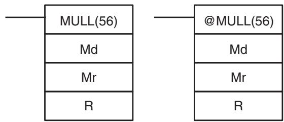
Operand Data Areas
| Md: First multiplicand word (BCD) |
| IR, SR, AR, DM, EM, HR, TIM/CNT, LR |
| Mr: First multiplier word (BCD) |
| IR, SR, AR, DM, EM, HR, TIM/CNT, LR |
| R: First result word |
| IR, SR, AR, DM, EM, HR, LR |
Limitations
DM 6141 to DM 6655 cannot be used for R.
Description
When the execution condition is OFF, MULL(56) is not executed. When the execution condition is ON, MULL(56) multiplies the eight-digit content of Md and Md+1 by the content of Mr and Mr+1, and places the result in R to R+3.
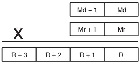
Flags
ER: Md, Md+1, Mr, or Mr+1 is not BCD.
Indirectly addressed EM/DM word is non-existent.
(Content of *EM/*DM word is not BCD, or the EM/DM area boundary has been exceeded.)
CY: ON when there is a carry in the result.
EQ: ON when the result is 0.
5-21-10 DOUBLE BCD DIVIDE – DIVL(57)
Ladder Symbols
| DIVL(57) | @DIVL(57) |
| Dd | Dd |
| Dr | Dr |
| R | R |
Operand Data Areas
| Dd: First dividend word (BCD) |
| IR, SR, AR, DM, EM, HR, TIM/CNT, LR |
| Dr: First divisor word (BCD) |
| IR, SR, AR, DM, EM, HR, TIM/CNT, LR |
| R: First result word |
| IR, SR, AR, DM, EM, HR, LR |
Limitations
DM 6141 to DM 6655 cannot be used for R.
Description
When the execution condition is OFF, DIVL(57) is not executed. When the execution condition is ON, DIVL(57) the eight-digit content of Dd and D+1 is divided by the content of Dr and Dr+1 and the result is placed in R to R+3: the quotient in R and R+1, the remainder in R+2 and R+3.
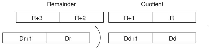
flowchart
graph TD
    A["Remainder"] --> B["R+3"]
    A --> C["R+2"]
    A --> D["Dr+1"]
    A --> E["Dr"]
    F["Quotient"] --> G["R+1"]
    F --> H["R"]
    F --> I["Dd+1"]
    F --> J["Dd"]
Flags
ER: Dr and Dr+1 contain 0.
Dd, Dd+1, Dr, or Dr+1 is not BCD.
Indirectly addressed EM/DM word is non-existent.
(Content of *EM/*DM word is not BCD, or the EM/DM area boundary has been exceeded.)
EQ: ON when the result is 0.
5-21-11 SQUARE ROOT - ROOT(72)
Ladder Symbols
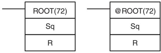
flowchart
graph TD
    A["ROOT(72)"] --> B["Sq"]
    A --> C["R"]
    D["@ROOT(72)"] --> E["Sq"]
    D --> F["R"]
Operand Data Areas
| Sq: First source word (BCD) |
| IR, SR, AR, DM, EM, HR, TIM/CNT, LR |
| R: Result word |
| IR, SR, AR, DM, EM, HR, LR |
Limitations
DM 6144 to DM 6655 cannot be used for R.
Description
When the execution condition is OFF, ROOT(72) is not executed. When the execution condition is ON, ROOT(72) computes the square root of the eight-digit content of Sq and Sq+1 and places the result in R. The fractional portion is truncated.
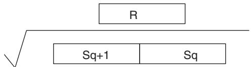
flowchart
graph TD
A["R"] --> B["Sq+1"]
A --> C["Sq"]
Flags
ER: Sq is not BCD.
Indirectly addressed EM/DM word is non-existent.
(Content of *EM/*DM word is not BCD, or the EM/DM area boundary has been exceeded.)
EQ: ON when the result is 0.
Example
The following example shows how to take the square root of an eight digit number. The result is a four-digit number, with the remainder rounded off. and then round the result.
In this example, 63250561 = 7953.0221 , which is rounded off to 7953.
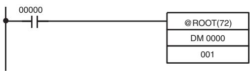
| Address | Instruction | Operands |
| 00000 | LD | 00000 |
| 00001 | @ROOT(72) | |
| DM 0000 | ||
| 001 |
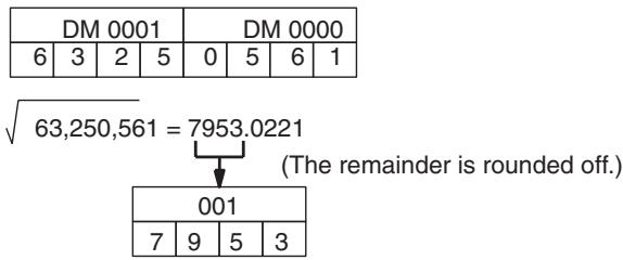
5-22 Binary Calculation Instructions
5-22-1 BINARY ADD - ADB(50)
Ladder Symbols
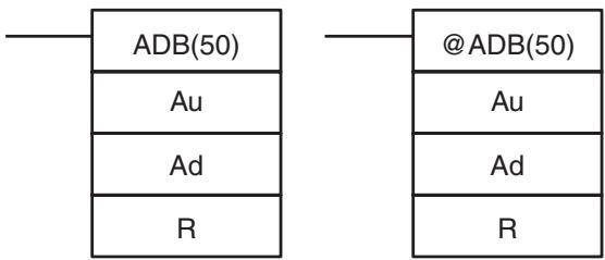
Operand Data Areas
| Au: Augend word (binary) |
| IR, SR, AR, DM, EM, HR, TIM/CNT, LR, # |
| Ad: Addend word (binary) |
| IR, SR, AR, DM, EM, HR, TIM/CNT, LR, # |
| R: Result word |
| IR, SR, AR, DM, EM, HR, LR |
Limitations
DM 6144 to DM 6655 cannot be used for R.
Description
When the execution condition is OFF, ADB(50) is not executed. When the execution condition is ON, ADB(50) adds the contents of Au, Ad, and CY, and places the result in R. CY will be set if the result is greater than FFFF.

ADB(50) can also be used to add signed binary data. The Overflow and Underflow Flags (SR 25404 and SR 25405) indicate whether the result has exceeded the lower or upper limits of the 16-bit signed binary data range.
Flags
ER: Indirectly addressed EM/DM word is non-existent.
(Content of *EM/*DM word is not BCD, or the EM/DM area boundary has been exceeded.)
CY: ON when the result is greater than FFFF.
EQ: ON when the result is 0.
OF: ON when the result exceeds +32,767 (7FFF).
UF: ON when the result is below -32,768 (8000).
Example
The following example shows a four-digit addition with CY used to place either #0000 or #0001 into R+1 to ensure that any carry is preserved.
flowchart
graph TD
A["00000"] --> B["TR 0"]
B --> C["CLC(41)"]
B --> D["ADB(50)"]
D --> E["010"]
D --> F["DM 0100"]
D --> G["HR 10"]
B --> H["25504"]
H --> I["MOV(21)"]
I --> J["#0000"]
I --> K["HR 11"]
B --> L["25504"]
L --> M["MOV(21)"]
M --> N["#0001"]
M --> O["HR 11"]
style A fill:#f9f,stroke:#333
style B fill:#ccf,stroke:#333
style C fill:#cfc,stroke:#333
style D fill:#fcc,stroke:#333
style E fill:#cff,stroke:#333
style F fill:#ffc,stroke:#333
style G fill:#fcc,stroke:#333
style H fill:#ffc,stroke:#333
style I fill:#cfc,stroke:#333
style J fill:#fcc,stroke:#333
style K fill:#fcc,stroke:#333
style L fill:#ffc,stroke:#333
style M fill:#cfc,stroke:#333
style N fill:#fcc,stroke:#333
style O fill:#fcc,stroke:#333
| Address | Instruction | Operands |
| 00000 | LD | 00000 |
| 00001 | OUT | TR 0 |
| 00002 | CLC(41) | |
| 00003 | ADB(50) | |
| 010 | ||
| DM 0100 | ||
| HR 10 | ||
| 00004 | AND NOT | 25504 |
| 00005 | MOV(21) | |
| # 0000 | ||
| HR 11 | ||
| 00006 | LD | TR 0 |
| 00007 | AND | 25504 |
| 00008 | MOV(21) | |
| # 00001 | ||
| HR 11 |
In the case below, A6E2 + 80C5 = 127A7. The result is a 5-digit number, so CY (SR 25504) = 1, and the content of R + 1 becomes #0001.
| Au: IR 010 | |||
| A | 6 | E | 2 |

| Ad: DM 0100 | |||
| 8 | 0 | C | 5 |
| R+1: HR 11 | R: HR 10 | ||||||
| 0 | 0 | 0 | 1 | 2 | 7 | A | 7 |
Note For signed binary calculations, the status of the UF and OF flags indicate whether the result has exceeded the signed binary data range (-32,768 (8000) to +32,767 (7FFF)).
5-22-2 BINARY SUBTRACT - SBB(51)
Ladder Symbols
| Mi: Minuend word (binary) |
| IR, SR, AR, DM, EM, HR, TIM/CNT, LR, # |
| Su: Subtrahend word (binary) |
| IR, SR, AR, DM, EM, HR, TIM/CNT, LR, # |
| R: Result word |
| IR, SR, AR, DM, EM, HR, LR |
Limitations
Description
DM 6144 to DM 6655 cannot be used for R.
When the execution condition is OFF, SBB(51) is not executed. When the execution condition is ON, SBB(51) subtracts the contents of Su and CY from Mi and places the result in R. If the result is negative, CY is set and the 2's complement of the actual result is placed in R.

SBB(51) can also be used to subtract signed binary data. The Overflow and Underflow Flags (SR 25404 and SR 25405) indicate whether the result has exceeded the lower or upper limits of the 16-bit signed binary data range.
Flags
ER: Indirectly addressed EM/DM word is non-existent.
(Content of *EM/*DM word is not BCD, or the EM/DM area boundary has been exceeded.)
CY: ON when the result is negative, i.e., when Mi is less than Su plus CY.
EQ: ON when the result is 0.
OF: ON when the result exceeds +32,767 (7FFF).
UF: ON when the result is below -32,768 (8000).
Example
The following example shows a four-digit subtraction. When IR 00001 is ON, the content of LR 00 and CY are subtracted from the content of IR 002 and the result is written to HR 01.
CY is turned ON if the result is negative. If normal data is being used, a negative result (signed binary) must be converted to normal data using NEG(—). Refer to 5-20-17 2'S COMPLEMENT – NEG(—) for details.
flowchart
graph TD
A["00001"] --> B["CLC(41)"]
A --> C["SBB(51)"]
C --> D["002"]
C --> E["LR00"]
C --> F["HR 01"]
| Address | Instruction | Operands |
| 00000 | LD | 00001 |
| 00001 | OUT | TR 1 |
| 00002 | CLC(41) | |
| 00003 | SBB(51) | |
| 002 | ||
| LR 00 | ||
| HR 01 |
In the case below, the content of LR 00 (#7A03) and CY are subtracted from IR 002 (#F8C5). Since the result is positive, CY is 0.
If the result had been negative, CY would have been set to 1. For normal (unsigned) data, the result would have to be converted to its 2's complement.
Note For signed binary calculations, the status of the UF and OF flags indicate whether the result has exceeded the signed binary data range (-32,768 (8000) to +32,767 (7FFF)).
5-22-3 BINARY MULTIPLY - MLB(52)
Ladder Symbols
flowchart
graph TD
A["MLB(52)"] --> B["Md"]
A --> C["Mr"]
A --> D["R"]
E["@MLB(52)"] --> F["Md"]
E --> G["Mr"]
E --> H["R"]
Operand Data Areas
| Md: Multiplicand word (binary) |
| IR, SR, AR, DM, EM, HR, TIM/CNT, LR, # |
| Mr: Multiplier word (binary) |
| IR, SR, AR, DM, EM, HR, TIM/CNT, LR, # |
| R: First result word |
| IR, SR, AR, DM, EM, HR, LR |
Limitations
DM 6143 to DM 6655 cannot be used for R.
MLB(52) cannot be used to multiply signed binary data, but MBS(—) can be used. Refer to 5-22-7 SIGNED BINARY MULTIPLY – MBS(—).
Description
When the execution condition is OFF, MLB(52) is not executed. When the execution condition is ON, MLB(52) multiplies the content of Md by the contents of Mr, places the rightmost four digits of the result in R, and places the leftmost four digits in R+1.
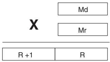
Flags
ER: Indirectly addressed EM/DM word is non-existent. (Content of *EM/*DM word is not BCD, or the EM/DM area boundary has been exceeded.)
EQ: ON when the result is 0.
5-22-4 BINARY DIVIDE – DVB(53)
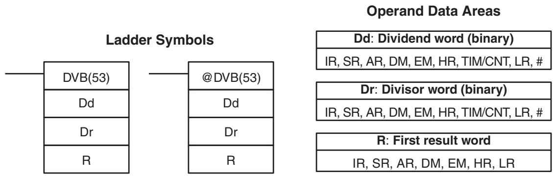
Limitations
DM 6143 to DM 6655 cannot be used for R.
DVB(53) cannot be used to divide signed binary data, but DBS(—) can be used. Refer to 5-22-9 SIGNED BINARY DIVIDE – DBS(—) for details.
Description
When the execution condition is OFF, DVB(53) is not executed. When the execution condition is ON, DVB(53) divides the content of Dd by the content of Dr and the result is placed in R and R+1: the quotient in R, the remainder in R+1.
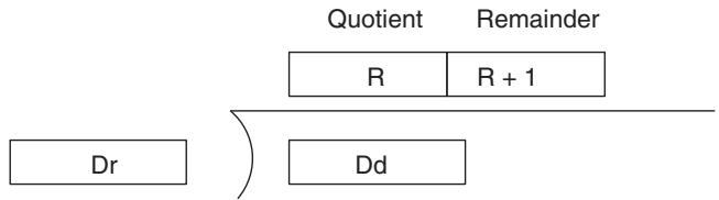
flowchart
graph TD
Dr["Dr"] --> R["R"]
Dr --> Dd["Dd"]
R --> R1["R + 1"]
R1 --> Remainder["Remainder"]
style Dr fill:#fff,stroke:#000
style R fill:#fff,stroke:#000
style Dd fill:#fff,stroke:#000
style Remainder fill:#fff,stroke:#000
Flags
ER: Dr contains 0.
Indirectly addressed EM/DM word is non-existent.
(Content of *EM/*DM word is not BCD, or the EM/DM area boundary has been exceeded.)
EQ: ON when the result is 0.
5-22-5 DOUBLE BINARY ADD - ADBL(—)
Ladder Symbols
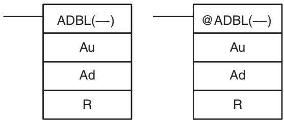
flowchart
graph TD
A["ADBL(---)"] --> B["Au"]
A --> C["Ad"]
A --> D["R"]
E["@ADBL(---)"] --> F["Au"]
E --> G["Ad"]
E --> H["R"]
Operand Data Areas
| Au: First augend word (binary) |
| IR, SR, AR, DM, EM, HR, TIM/CNT, LR, # |
| Ad: First addend word (binary) |
| IR, SR, AR, DM, EM, HR, TIM/CNT, LR, # |
| R: First result word |
| IR, SR, AR, DM, EM, HR, LR |
Limitations
Au and Au+1 must be in the same data area, as must Ad and Ad+1, and R and R+1.
DM 6142 to DM 6655 cannot be used for R.
Description
When the execution condition is OFF, ADBL(—) is not executed. When the execution condition is ON, ADBL(—) adds the eight-digit contents of Au+1 and Au, the eight-digit contents of Ad+1 and Ad, and CY, and places the result in R. CY will be set if the result is greater than FFFF FFFF.
| Au + 1 | Au |
| Ad + 1 | Ad |

CY
| CY | R+1 | R |
ADBL(—) can also be used to add signed binary data. The Overflow and Underflow Flags (SR 25404 and SR 25405) indicate whether the result has exceeded the lower or upper limits of the 32-bit signed binary data range.
Flags
ER: Indirectly addressed EM/DM word is non-existent.
(Content of *EM/*DM word is not BCD, or the EM/DM area boundary has been exceeded.)
CY: ON when the result is greater than FFFF FFFF.
EQ: ON when the result is 0.
OF: ON when the result exceeds +2,147,483,647 (7FFF FFFF).
UF: ON when the result is below -2,147,483,648 (8000 0000).
Example
The following example shows an eight-digit addition with CY (SR 25504) used to represent the status of the 9th digit. The status of the UF and OF flags indicate whether the result has exceeded the signed binary data range (-2,147,483,648 (8000 0000) to +2,147,483,647 (7FFF FFFF)).
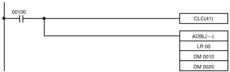
flowchart
graph TD
A["00100"] --> B["CLC(41)"]
A --> C["ADBL(—)"]
C --> D["LR 00"]
C --> E["DM 0010"]
C --> F["DM 0020"]
| Address | Instruction | Operands |
| 00000 | LD | 00100 |
| 00001 | CLC(41) | |
| 00002 | ADBL(—) | |
| LR 20 | ||
| DM 0010 | ||
| DM 0020 |
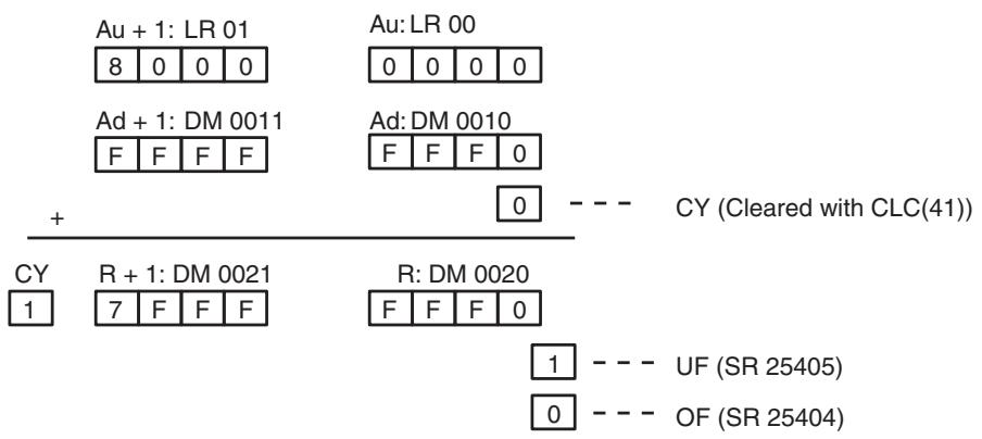
Note 1. For unsigned binary addition, CY indicates that the sum of the two values exceeds FFFF FFFF. (UF and OF can be ignored.)
- For signed binary addition, the UF flag indicates that the sum of the two values is below -2,147,483,648 (8000 0000). (CY can be ignored.)
5-22-6 DOUBLE BINARY SUBTRACT – SBBL(—)
Operand Data Areas
| Ladder Symbols | |
| SBBL(--) | @SBBL(--) |
| Mi | Mi |
| Su | Su |
| R | R |
Limitations
Mi and Mi+1 must be in the same data area, as must Su and Su+1, and R and R+1.
DM 6142 to DM 6655 cannot be used for R.
Description
When the execution condition is OFF, SBBL(—) is not executed. When the execution condition is ON, SBBL(—) subtracts CY and the eight-digit value in Su and Su+1 from the eight-digit value in Mi and Mi+1, and places the result in R and R+1. If the result is negative, CY is set and the 2's complement of the actual result is placed in R+1 and R. Use NEGL(—) to convert the 2's complement to the true result.
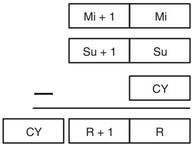
flowchart
graph TD
A["Mi + 1"] --> B["Su + 1"]
C["Mi"] --> D["Su"]
E["CY"] --> F["R + 1"]
G["R"] --> H["CY"]
SBBL(—) can also be used to subtract signed binary data. The Overflow and Underflow Flags (SR 25404 and SR 25405) indicate whether the result has exceeded the lower or upper limits of the 32-bit signed binary data range.
Flags
ER: Indirectly addressed EM/DM word is non-existent.
(Content of *EM/*DM word is not BCD, or the EM/DM area boundary has been exceeded.)
CY: ON when the result is negative, i.e., when Mi is less than Su plus CY.
EQ: ON when the result is 0.
OF: ON when the result exceeds +2,147,483,647 (7FFF FFFF).
UF: ON when the result is below -2,147,483,648 (8000 0000).
Example
The following example shows an eight-digit subtraction with CY (SR 25504) used to indicate a negative result (with unsigned data). The status of the UF and OF flags indicate whether the result has exceeded the signed binary data range (-2,147,483,648 (8000 0000) to +2,147,483,647 (7FFF FFFF)).
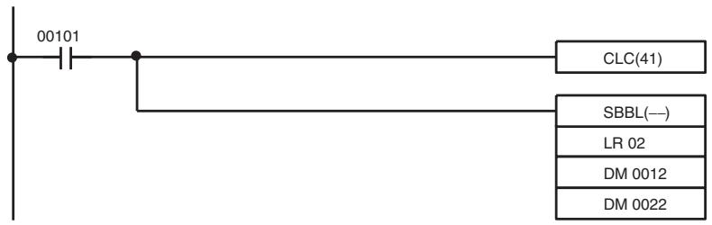
flowchart
graph TD
A["00101"] --> B["CLC(41)"]
A --> C["SBBL(---)"]
C --> D["LR 02"]
C --> E["DM 0012"]
C --> F["DM 0022"]
| Address | Instruction | Operands |
| 00000 | LD | 00101 |
| 00001 | CLC(41) | |
| 00002 | SBBL(—) | |
| LR 22 | ||
| DM 0012 | ||
| DM 0022 |
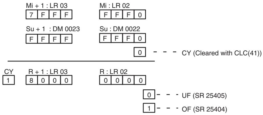
Note
- For unsigned binary data, CY indicates that the result is negative. Take the 2's complement using NEGL(—) to obtain the absolute value of the true result. (UF and OF can be ignored.)
- For signed binary data, the OF flag indicates that the result exceeds +2,147,483,647 (7FFF FFFF). (CY can be ignored.)
5-22-7 SIGNED BINARY MULTIPLY - MBS(—)
Ladder Symbols
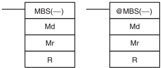
flowchart
graph TD
A["MBS(—)"] --> B["Md"]
A --> C["Mr"]
A --> D["R"]
E["@MBS(—)"] --> F["Md"]
E --> G["Mr"]
E --> H["R"]
Operand Data Areas
| Md: Multiplicand word |
| IR, SR, AR, DM, EM, HR, TIM/CNT, LR, # |
| Mr: Multiplier word |
| IR, SR, AR, DM, EM, HR, TIM/CNT, LR, # |
| R: First result word |
| IR, SR, AR, DM, EM, HR, LR |
Limitations
DM 6143 to DM 6655 cannot be used for R.
Description
MBS(—) multiplies the signed binary content of two words and outputs the 8-digit signed binary result to R+1 and R. The rightmost four digits of the result are placed in R, and the leftmost four digits are placed in R+1.
Note Refer to 1-7 Calculating with Signed Binary Data for more details.
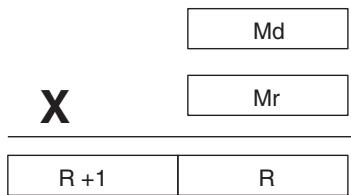
flowchart
graph TD
A["X"] --> B["Md"]
A --> C["Mr"]
D["R +1"] --> E["R"]
Flags
ER: Indirectly addressed EM/DM word is non-existent.
(Content of *EM/*DM word is not BCD, or the EM/DM area boundary has been exceeded.)
EQ: ON when the result is 0000 0000, otherwise OFF.
Example
In the following example, MBS(—) is used to multiply the signed binary contents of DM 0010 with the signed binary contents of DM 0012 and output the result to DM 0100 and DM 0101.
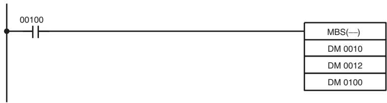
| Address | Instruction | Operands |
| 00000 | LD | 00100 |
| 00001 | MBS(—) | |
| DM 0010 | ||
| DM 0012 | ||
| DM 0100 |
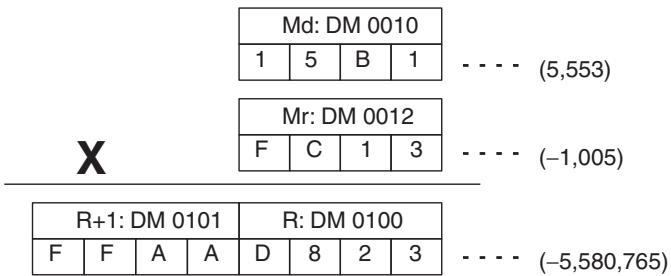
5-22-8 DOUBLE SIGNED BINARY MULTIPLY - MBSL(—)
Ladder Symbols
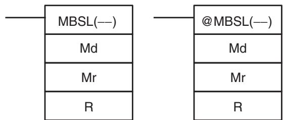
flowchart
graph TD
A["MBSL(---)"] --> B["Md"]
A --> C["Mr"]
A --> D["R"]
E["@MBSL(---)"] --> F["Md"]
E --> G["Mr"]
E --> H["R"]
Operand Data Areas
| Md: First multiplicand word |
| IR, SR, AR, DM, EM, HR, TIM/CNT, LR, # |
| Mr: First multiplier word |
| IR, SR, AR, DM, EM, HR, TIM/CNT, LR, # |
| R: First result word |
| IR, SR, AR, DM, EM, HR, LR |
Limitations
Md and Md+1 must be in the same data area, as must Mr and Mr+1.
R and R+3 must be in the same data area.
DM 6143 to DM 6655 cannot be used for R.
Description
MBSL(—) multiplies the 32-bit (8-digit) signed binary data in Md+1 and Md with the 32-bit signed binary data in Mr+1 and Mr, and outputs the 16-digit signed binary result to R+3 through R.
Note Refer to 1-7 Calculating with Signed Binary Data for more details.

flowchart
graph TD
A["X"] --> B["Md + 1"]
A --> C["Mr + 1"]
B --> D["Md"]
C --> E["Mr"]
F["R + 3"] --> G["R + 2"]
H["R + 1"] --> I["R"]
Flags
ER: Indirectly addressed EM/DM word is non-existent.
(Content of *EM/*DM word is not BCD, or the EM/DM area boundary has been exceeded.)
EQ: ON when the result is zero (content of R+3 through R all zeroes), otherwise OFF.
Example
In the following example, MBSL(—) is used to multiply the signed binary contents of IR 101 and IR 100 with the signed binary contents of DM 0021 and DM 0020 and output the result to LR 24 through LR 01.
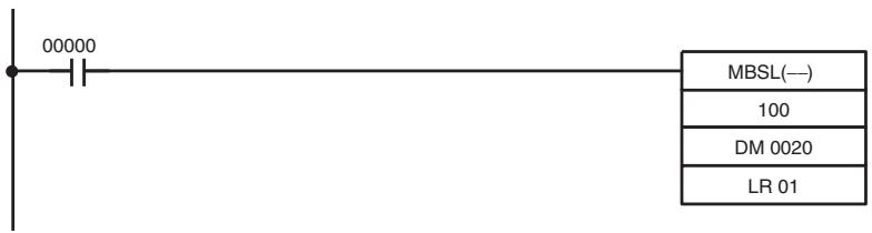
| Address | Instruction | Operands |
| 00000 | LD | 00000 |
| 00001 | MBSL(—) | |
| 100 | ||
| DM 0020 | ||
| LR 21 |
| Md+1: IR 101 | Md: IR 100 | - - - (555,320) | ||||||
| 0 | 0 | 0 | 8 | 7 | 9 | 3 | 8 | |
| Mr+1: DM 0021 | Mr: DM 0020 | - - - (-1,005,550) | ||||||
| F | F | F | 0 | A | 8 | 1 | 2 | |
| R+1: LR 02 | R: LR 01 | - - - (-55,840,206,000) | ||||||
| F | C | A | 5 | 4 | 5 | F | 0 | |
5-22-9 SIGNED BINARY DIVIDE - DBS(—)
Ladder Symbols
| DBS(—) | @DBS(—) |
| Dd | Dd |
| Dr | Dr |
| R | R |
Operand Data Areas
| Dd: Dividend word |
| IR, SR, AR, DM, EM, HR, TIM/CNT, LR, # |
| Dr: Divisor word |
| IR, SR, AR, DM, EM, HR, TIM/CNT, LR, # |
| R: First result word |
| IR, SR, AR, DM, EM, HR, LR |
Limitations
DM 6143 to DM 6655 cannot be used for R.
Description
DBS(—) divides the signed binary content of Dd by the signed binary content of Dr, and outputs the 8-digit signed binary result to R+1 and R. The quotient is placed in R, and the remainder is placed in R+1.
Note Refer to 1-7 Calculating with Signed Binary Data for more details.
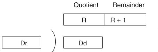
flowchart
graph TD
Dr["Dr"] --> R["R"]
Dr --> Dd["Dd"]
R --> Remainder["Remainder"]
R + 1["R + 1"]
Flags
ER: Dr contains 0.
Indirectly addressed EM/DM word is non-existent.
(Content of *EM/*DM word is not BCD, or the EM/DM area boundary has been exceeded.)
EQ: ON when the content of R (the quotient) is 0000, otherwise OFF.
Example
In the following example, DBS(—) is used to divide the signed binary contents of DM 0010 with the signed binary contents of DM 0020 and output the result to LR 21 and LR 02.
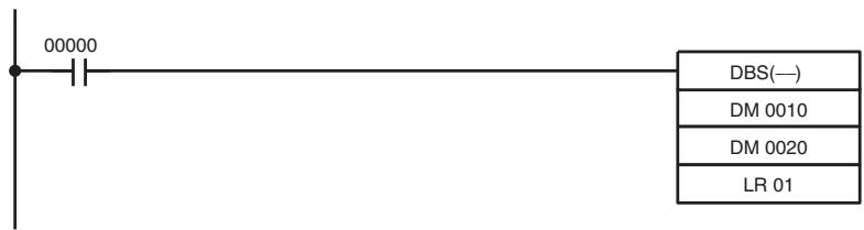
| Address | Instruction | Operands |
| 00000 | LD | 00000 |
| 00001 | DBS(---) | |
| DM 0010 | ||
| DM 0020 | ||
| LR 21 |
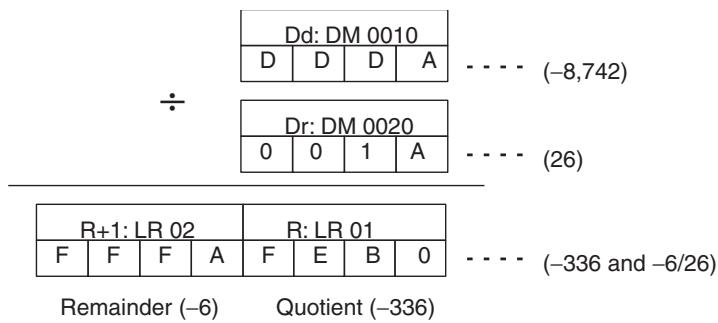
5-22-10 DOUBLE SIGNED BINARY DIVIDE – DBSL(—)
Operand Data Areas
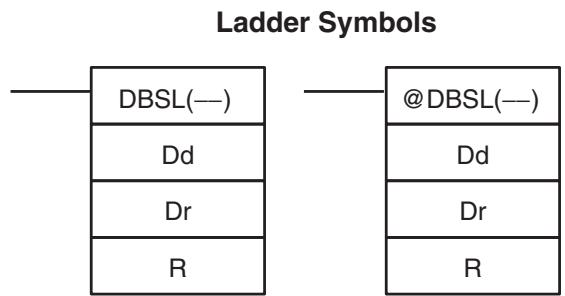
flowchart
graph TD
A["DBSL(—)"] --> B["Dd"]
A --> C["Dr"]
A --> D["R"]
E["@DBSL(—)"] --> F["Dd"]
E --> G["Dr"]
E --> H["R"]
| Dd: First dividend word (binary) |
| IR, SR, AR, DM, EM, HR, TIM/CNT, LR, # |
| Dr: First divisor word (binary) |
| IR, SR, AR, DM, EM, HR, TIM/CNT, LR, # |
| R: First result word |
| IR, SR, AR, DM, EM, HR, LR |
Limitations
Dd and Dd+1 must be in the same data area, as must Dr and Dr+1.
R and R+3 must be in the same data area.
DM 6143 to DM 6655 cannot be used for R.
Description
DBS(—) divides the 32-bit (8-digit) signed binary data in Dd+1 and Dd by the 32-bit signed binary data in Dr+1 and Dr, and outputs the 16-digit signed binary result to R+3 through R. The quotient is placed in R+1 and R, and the remainder is placed in R+3 and R+2.
Note Refer to 1-7 Calculating with Signed Binary Data for more details.
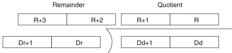
flowchart
graph TD
A["Remainder"] --> B["R+3"]
A --> C["R+2"]
A --> D["Dr+1"]
A --> E["Dr"]
F["Quotient"] --> G["R+1"]
F --> H["Dd+1"]
F --> I["Dd"]
Flags
ER: Dr+1 and Dr contain 0.
Indirectly addressed EM/DM word is non-existent.
(Content of *EM/*DM word is not BCD, or the EM/DM area boundary has been exceeded.)
EQ: ON when the content of R+1 and R (the quotient) is 0, otherwise OFF.
Example
In the following example, DBSL(—) is used to divide the signed binary contents of IR 101 and IR 100 with the signed binary contents of DM 0021 and DM 0020 and output the result to LR 24 through LR 01.
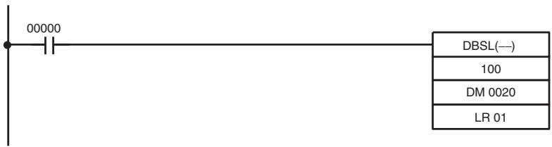
| Address | Instruction | Operands |
| 00000 | LD | 00000 |
| 00001 | DBSL(—) | |
| 100 | ||
| DM 0020 | ||
| LR 21 |
| Dd+1: IR 101 | Dd: IR 100 | ||||||
| F | F | 7 | A | B | 1 | 5 | C |
| - - - (-8,736,420) | |||||||
| Dr+1: DM 0021 | Dr: DM 0020 | ||||||
| 0 | 0 | 0 | 0 | 0 | 0 | 1 | A |
| - - - (26) | |||||||
| R+3: LR 04 | R+2: LR 03 | R+1: LR 02 | R: LR 01 | ||||||||||||
| F | F | F | F | F | F | F | C | F | F | F | A | D | F | 7 | 0 |
| Remainder (-4) Quotient (-336) | |||||||||||||||
5-23 Special Math Instructions
| C: Control data |
| IR, SR, AR, DM, EM, HR, TIM/CNT, LR, # |
| R1: First word in range |
| IR, SR, AR, DM, EM, HR, TIM/CNT, LR |
| D: Destination word |
| IR, SR, AR, DM, EM, HR, LR |
Limitations
N must be BCD between 0001 to 9999.
R_1 and R_1+N-1 must be in the same data area.
DM 6144 to DM 6655 cannot be used for D.
Description
When the execution condition is OFF, MAX(—) is not executed. When the execution condition is ON, MAX(—) searches the range of memory from R_1 to R_1+N-1 for the address that contains the maximum value and outputs the maximum value to the destination word (D).
If bit 15 of C is ON, MAX(—) identifies the address of the word containing the maximum value in D+1. The address is identified differently for the DM area:
1,2,3...
- For an address in the DM area, the word address is written to C+1. For example, if the address containing the maximum value is DM 0114, then #0114 is written in D+1.
- For an address in another data area, the number of addresses from the beginning of the search is written to D+1. For example, if the address containing the maximum value is IR 114 and the first word in the search range is IR 014, then #0100 is written in D+1.
If bit 14 of C is ON and more than one address contains the same maximum value, the position of the lowest of the addresses will be output to D+1. The position will be output as the DM address for the DM area, but as an absolute position relative to the first word in the range for all other areas.
The number of words within the range (N) is contained in the 3 rightmost digits of C, which must be BCD between 001 and 999.
When bit 15 of C is OFF, data within the range is treated as unsigned binary and when it is ON the data is treated as signed binary.
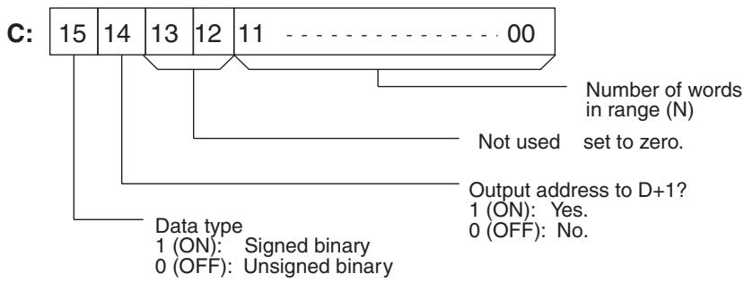
Caution
If bit 14 of C is ON, values above #8000 are treated as negative numbers, so the results will differ depending on the specified data type. Be sure that the correct data type is specified.
Flags
ER: Indirectly addressed EM/DM word is non-existent.
(Content of *EM/*DM word is not BCD, or the EM/DM area boundary has been exceeded.)
R_1 and R_1+N-1 are not in the same data area.
EQ: ON when the maximum value is #0000.
5-23-2 FIND MINIMUM - MIN(—)
Ladder Symbols
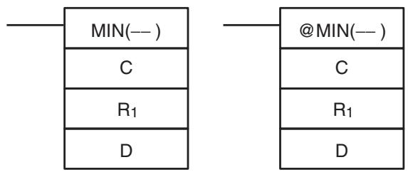
Limitations
N must be BCD between 0001 to 9999.
R_1 and R_1+N-1 must be in the same data area.
DM 6144 to DM 6655 cannot be used for D.
Description
When the execution condition is OFF, MIN(—) is not executed. When the execution condition is ON, MIN(—) searches the range of memory from R_1 to R_1+N-1 for the address that contains the minimum value and outputs the minimum value to the destination word (D).
If bit 15 of C is ON, MIN(—) identifies the address of the word containing the minimum value in D+1. The address is identified differently for the DM area:
1,2,3...
- For an address in the DM area, the word address is written to C+1. For example, if the address containing the minimum value is DM 0114, then #0114 is written in D+1.
- For an address in another data area, the number of addresses from the beginning of the search is written to D+1. For example, if the address containing the minimum value is IR 114 and the first word in the search range is IR 014, then #0100 is written in D+1.
If bit 14 of C is ON and more than one address contains the same minimum value, the position of the lowest of the addresses will be output to D+1. The position will be output as the DM address for the DM area, but as an absolute position relative to the first word in the range for all other areas.
The number of words within the range (N) is contained in the 3 rightmost digits of C, which must be BCD between 001 and 999.
When bit 15 of C is OFF, data within the range is treated as unsigned binary and when it is ON the data is treated as signed binary.
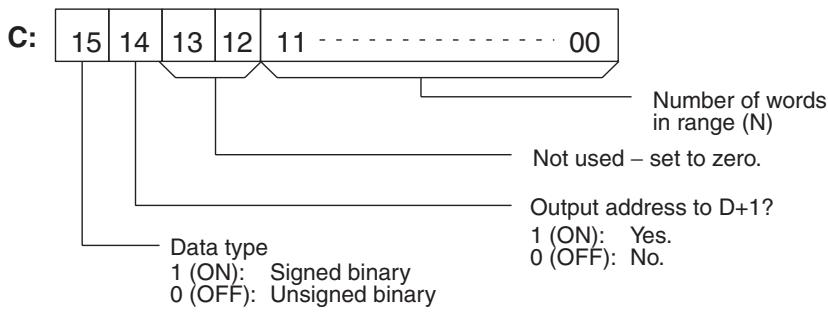
Caution
If bit 14 of C is ON, values above #8000 are treated as negative numbers, so the results will differ depending on the specified data type. Be sure that the correct data type is specified.
Flags
ER: Indirectly addressed EM/DM word is non-existent.
(Content of *EM/*DM word is not BCD, or the EM/DM area boundary has been exceeded.)
R_1 and R_1+N-1 are not in the same data area.
EQ: ON when the minimum value is #0000.
5-23-3 AVERAGE VALUE - AVG(—)
Ladder Symbols
| AVG(—) |
| S |
| N |
| D |
Operand Data Areas
| S: Source word |
| IR, SR, AR, DM, EM, HR, TIM/CNT, LR |
| N: Number of cycles |
| IR, SR, AR, DM, EM, HR, TIM/CNT, LR, # |
| D: First destination word |
| IR, SR, AR, DM, EM, HR, LR |
Limitations
S must be hexadecimal.
N must be BCD from #0001 to #0064.
D and D+N+1 must be in the same data area.
DM 6144 to DM 6655 cannot be used for S, N, or D to D+N+1.
Description
AVG(—) is used to calculate the average value of S over N cycles.
When the execution condition is OFF, AVG(—) is not executed.
Each time that AVG(—) is executed, the content of S is stored in words D+2 to D+N+1. On the first execution, AVG(—) writes the content of S to D+2; on the second execution it writes the content of S to D+3, etc. On the Nth execution, AVG(—) writes the content of S stored in D+N+1, AVG(—) calculates the average value of the values stored in D+2 to D+N+1, and writes the average to D.
The following diagram shows the function of words D to D+N+1.
| D | Average value (after N or more executions) |
| D+1 | Used by the system. |
| D+2 | Content of S from the 1st execution of AVG(--) |
| D+3 | Content of S from the 2nd execution of AVG(--) |
| D+N+1 | Content of S from the Nth execution of AVG(--) |
Precautions
The average value is calculated in binary. Be sure that the content of S is in binary.
N must be BCD from #0001 to #0064. If the content of N ≥ #0065, AVG(—) will operate with N=64.
The average value will be rounded off to the nearest integer value. (0.5 is rounded up to 1.)
Leave the contents of D+1 set to #0000 after the first execution of AVG(—).
Flags
ER: Indirectly addressed EM/DM word is non-existent.
(Content of *EM/*DM word is not BCD, or the EM/DM area boundary has been exceeded.)
One or more operands have been set incorrectly.
D and D+N+1 are not in the same data area.
Example
In the following example, the content of IR 040 is set to #0000 and then incremented by 1 each cycle. For the first two cycles, AVG(—) moves the content of IR 040 to DM 1002 and DM 1003. On the third and later cycles AVG(—) calculates the average value of the contents of DM 1002 to DM 1004 and writes that average value to DM 1000.
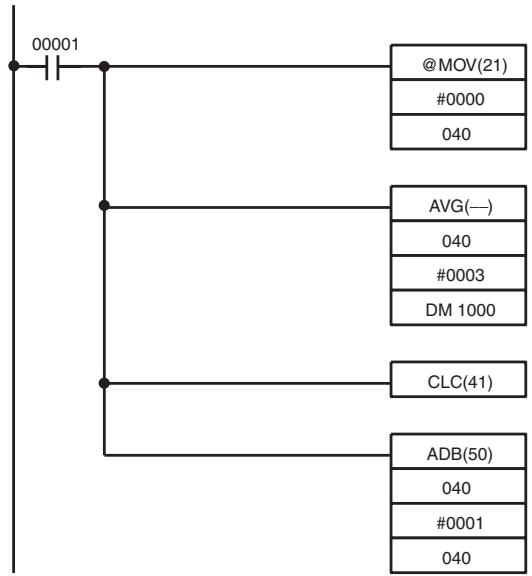
flowchart
graph TD
A["00001"] --> B["@MOV(21)"]
B --> C["#0000"]
B --> D["040"]
A --> E["AVG(—)"]
E --> F["040"]
E --> G["#0003"]
G --> H["DM 1000"]
A --> I["CLC(41)"]
I --> J["ADB(50)"]
J --> K["040"]
J --> L["#0001"]
L --> M["040"]
| Address | Instruction | Operands |
| 00000 | LD | 00001 |
| 00001 | @MOV(21) | |
| # 0000 | ||
| 040 | ||
| 00002 | AVG(—) | |
| 040 | ||
| # 0003 | ||
| DM 1000 | ||
| 00003 | CLC(41) | |
| 00004 | ADB(50) | |
| 040 | ||
| # 0001 | ||
| 040 |
| 1st cycle | 2nd cycle | 3rd cycle | 4th cycle | |
| IR 040 | 0000 | 0001 | 0002 | 0003 |
| 1st cycle | 2nd cycle | 3rd cycle | 4th cycle | |
| DM 1000 | 0000 | 0001 | 0001 | 0002 |
| DM 1001 | ||||
| DM 1002 | 0000 | 0000 | 0000 | 0003 |
| DM 1003 | --- | 0001 | 0001 | 0001 |
| DM 1004 | --- | --- | 0002 | 0002 |
5-23-4 SUM - SUM(—)
Ladder Symbols

flowchart
graph TD
A["SUM(--)"] --> B["C"]
A --> C["R1"]
A --> D["D"]
E["@SUM(--)"] --> F["C"]
E --> G["R1"]
E --> H["D"]
Operand Data Areas
| C: Control data |
| IR, SR, AR, DM, EM, HR, LR, # |
| R1: First word in range |
| IR, SR, AR, DM, EM, HR, TIM/CNT, LR |
| D: First destination word |
| IR, SR, AR, DM, EM, HR, LR |
Limitations
The 3 rightmost digits of C must be BCD between 001 and 999.
DM 6143 to DM 6655 cannot be used for D.
If bit 14 of C is OFF (setting for BCD data), all data within the range R_1 to R_1+N-1 must be BCD.
Description
When the execution condition is OFF, SUM(—) is not executed. When the execution condition is ON, SUM(—) adds either the contents of words R_1 to R_1+N-1 or the bytes in words R_1 to R_1+N/2-1 and outputs that value to the destination words (D and D+1). The data can be summed as binary or BCD and will be output in the same form. Binary data can be either signed or unsigned.
The function of bits in C are shown in the following diagram and explained in more detail below.
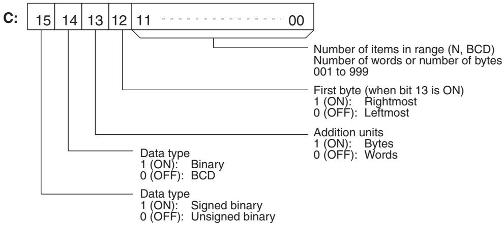
Number of Items in Range
The number of items within the range (N) is contained in the 3 rightmost digits of C, which must be BCD between 001 and 999. This number will indicate the number of words or the number of bytes depending the items being summed.
Addition Units
Words will be added if bit 13 is OFF and bytes will be added if bit 13 is ON. If bytes are specified, the range can begin with the leftmost or rightmost byte of R_1 . The leftmost byte of R_1 will not be added if bit 12 is ON.
The bytes will be added in this order when bit 12 is OFF: 1+2+3+4....
The bytes will be added in this order when bit 12 is ON: 2+3+4....
Data Type
Data within the range is treated as unsigned binary when bit 14 of C is ON and bit 15 is OFF, and it is treated as signed binary when both bits 14 and 15 are ON.
Data within the range is treated as BCD when bit 14 of C is OFF, regardless of the status of bit 15.
Flags
ER: Indirectly addressed EM/DM word is non-existent.
(Content of *EM/*DM word is not BCD, or the EM/DM area boundary has been exceeded.)
R_1 and R_1+N-1 are not in the same data area.
The number of items in C is not BCD between 001 and 999.
The data being summed is not BCD when BCD was designated.
EQ: ON when the result is zero.
Example
In the following example, the BCD contents of the 8 words from DM 0000 to DM 0007 are added when IR 00001 is ON and the result is written to DM 0010 and DM 0011.
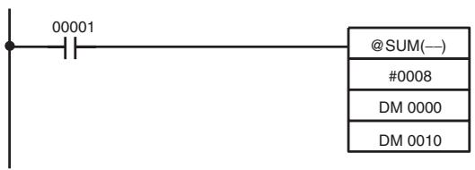
| Address | Instruction | Operands |
| 00000 | LD | 00001 |
| 00001 | @SUM(--) | |
| # 0008 | ||
| DM 0000 | ||
| DM 0010 |
| C: Contr ol w ord |
| IR, SR, AR, DM, EM, HR, TIM/CNT, LR, # |
| S: Input data source word |
| IR, SR, AR, DM, EM, HR, TIM/CNT, LR |
| D: Result destination word |
| IR, SR, AR, DM, EM, HR,TIM/CNT, LR |
Limitations
For trigonometric functions S must be BCD from 0000 to 0900 ( 0^ ≤ ≤ 90^ ). DM 6144 to DM 6655 cannot be used for D.
Description
When the execution condition is OFF, APR(—) is not executed. When the execution condition is ON, the operation of APR(—) depends on the control word C.
If C is #0000 or #0001, APR(—) computes () or ()^* . The BCD value of S specifies in tenths of degrees.
If C is an address, APR(—) computes f(x) of the function entered in advance beginning at word C. The function is a series of line segments (which can approximate a curve) determined by the operator. The BCD or hexadecimal value of S specifies x.
Flags
ER: Indirectly addressed EM/DM word is non-existent. (Content of *EM/*DM word is not BCD, or the EM/DM area boundary has been exceeded.) For trigonometric functions, x > 0900. (x is the content of S.) A constant other than #0000 or #0001 was designated for C. The linear approximation data is not readable.
EQ: The result is 0000.
Examples
Sine Function
The following example demonstrates the use of the APR(—) sine function to calculate the sine of 30^ . The sine function is specified when C is #0000.
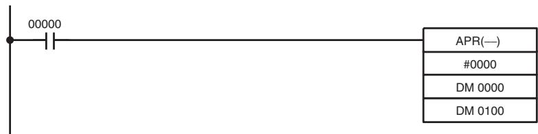
| Address | Instruction | Operands |
| 00000 | LD | 00000 |
| 00001 | APR(---) | |
| # 0000 | ||
| DM 0000 | ||
| DM 0100 |
Input data, x
| S: DM 0000 | |||
| 0 | 10^1 | 10^0 | 10^-1 |
| 0 | 3 | 0 | 0 |
Enter input data not exceeding #0900 in BCD.
Result data
| D: DM 0100 | |||
| 10^-1 | 10^-2 | 10^-3 | 10^-4 |
| 5 | 0 | 0 | 0 |
Result data has four significant digits, fifth and higher digits are ignored. The result for (90) will be 0.9999, not 1.
Cosine Function
The following example demonstrates the use of the APR(—) cosine function to calculate the cosine of 30^ . The cosine function is specified when C is #0001.
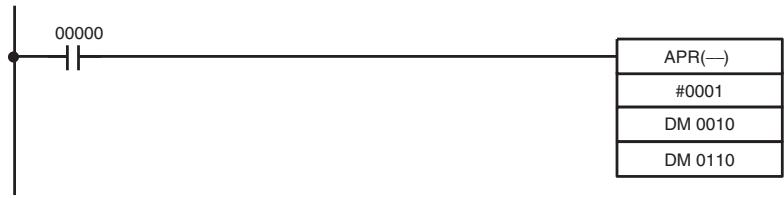
| Address | Instruction | Operands |
| 00000 | LD | 00000 |
| 00001 | APR(—) | |
| # 0001 | ||
| DM 0010 | ||
| DM 0110 |
Input data, x
| S: DM 0010 | |||
| 0 | 10^1 | 10^0 | 10^-1 |
| 0 | 3 | 0 | 0 |
Enter input data not exceeding #0900 in BCD.
Result data
| D: DM 0110 | |||
| 10^-1 | 10^-2 | 10^-3 | 10^-4 |
| 8 | 6 | 6 | 0 |
Result data has four significant digits, fifth and higher digits are ignored. The result for (0) will be 0.9999, not 1.
Linear Approximation
APR(—) linear approximation is specified when C is a memory address. Word C is the first word of the continuous block of memory containing the linear approximation data.
The content of word C specifies the number of line segments in the approximation, and whether the input and output are in BCD or BIN form. Bits 00 to 07 contain the number of line segments less 1, m-1, as binary data. Bits 14 and 15 determine, respectively, the output and input forms: 0 specifies BCD and 1 specifies BIN.
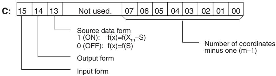
Enter the coordinates of the m+1 end-points, which define the m line segments, as shown in the following table. Enter all coordinates in BIN form. Always enter the coordinates from the lowest X value ( X_1 ) to the highest ( X_m ). X_0 is 0000, and does not have to be entered.
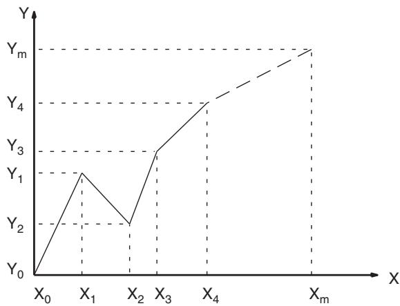
line
| X | Y | | ---- | ----- | | X₀ | Y₀ | | X₁ | Y₁ | | X₂ | Y₂ | | X₃ | Y₃ | | X₄ | Y₄ | | Xₘ | Yₘ || Word | Coordinate |
| C+1 | X_m (max. X value) |
| C+2 | Y_0 |
| C+3 | X_1 |
| C+4 | Y_1 |
| C+5 | X_2 |
| C+6 | Y_2 |
| ↓ | ↓ |
| C+(2m+1) | X_m |
| C+(2m+2) | Y_m |
If bit 13 of C is set to 1, the graph will be reflected from left to right, as shown in the following diagram.
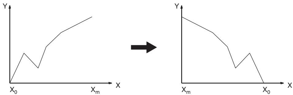
line
| X | Y | |-------|-------| | X₀ | 0 | | | Y | | | X_m | | | X₀ |The following example demonstrates the construction of a linear approximation with 12 line segments. The block of data is continuous, as it must be, from DM 0000 to DM 0026 (C to C + (2 × 12 + 2)). The input data is taken from IR 010, and the result is output to IR 011.
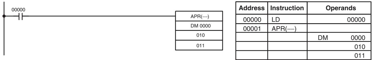
flowchart
graph LR
A["00000"] --> B["APR(---)"]
B --> C["DM 0000"]
C --> D["010"]
D --> E["011"]
F["Address"] --> G["Instruction"] --> H["Operands"]
I["00000"] --> J["LD"] --> K["00000"]
L["00001"] --> M["APR(---)"] --> N["DM 0000"]
O[" "] --> P["DM 010"]
Q[" "] --> R["DM 011"]
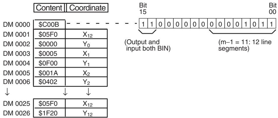
other
| DM | Content | Coordinate | |--------|---------|----------| | DM 0000 | $C00B | | | DM 0001 | $05F0 | X₁₂ | | DM 0002 | $0000 | Y₀ | | DM 0003 | $0005 | X₁ | | DM 0004 | $0F00 | Y₁ | | DM 0005 | $001A | X₂ | | DM 0006 | $0402 | Y₂ | | DM 0025 | $05F0 | X₁₂ | | DM 0026 | $1F20 | Y₁₂ |In this case, the input data word, IR 010, contains #0014, and f(0014) = #0726 is output to R, IR 011.
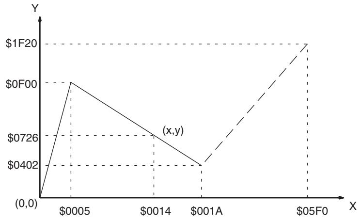
line
| X | Y | |---|---| | 0005 |0F00 | | 0014 |0726 | | 001A |0402 | | 05F0 |1F20 |5-24 Floating-point Math Instructions
The Floating-point Math Instructions convert data and perform floating-point arithmetic operations. CQM1H-series CPUs support the following instructions.
| Instruction | Mnemonic | Function code | Page |
| FLOATING TO 16-BIT | FIX | — | 352 |
| FLOATING TO 32-BIT | FIXL | — | 353 |
| 16-BIT TO FLOATING | FLT | — | 354 |
| 32-BIT TO FLOATING | FLTL | — | 355 |
| FLOATING-POINT ADD | +F | — | 355 |
| FLOATING-POINT SUBTRACT | -F | — | 357 |
| FLOATING-POINT MULTIPLY | *F | — | 358 |
| FLOATING-POINT DIVIDE | /F | — | 359 |
| DEGREES TO RADIANS | RAD | — | 360 |
| RADIANS-TO-DEGREES | DEG | — | 361 |
| SINE | SIN | — | 362 |
| COSINE | COS | — | 363 |
| TANGENT | TAN | — | 364 |
| ARC SINE | ASIN | — | 365 |
| ARC COSINE | ACOS | — | 366 |
| ARC TANGENT | ATAN | — | 367 |
| SQUARE ROOT | SQRT | — | 369 |
| EXPONENT | EXP | — | 370 |
| LOGARITHM | LOG | — | 371 |
Data Format
Floating-point data expresses real numbers using a sign, exponent, and mantissa. When data is expressed in floating-point format, the following formula applies.
$$ \text { Real number } = (- 1) ^ {s} 2 ^ {e - 1 2 7} (1. f) $$
s: Sign
e: Exponent
f: Mantissa
The floating-point data format conforms to the IEEE754 standards. Data is expressed in 32 bits, as follows:
| Sign | Exponent | Mantissa | |||
| s | e | f | |||
| 31 | 30 | 23 | 22 | 0 | |
| Data | No. of bits | Contents |
| s: sign | 1 | 0: positive; 1: negative |
| e: exponent | 8 | The exponent (e) value ranges from 0 to 255. The actual exponent is the value remaining after 127 is subtracted from e, resulting in a range of -127 to 128. “e=0” and “e=255” express special numbers. |
| f: mantissa | 23 | The mantissa portion of binary floating-point data fits the formal 2.0 > 1.f ≥ 1.0 . |
Number of Digits
The number of effective digits for floating-point data is 24 bits for binary (approximately seven digits decimal).
Floating-point Data
The following data can be expressed by floating-point data:
• -∞
- -3.402823 × 10^38 ≤ value ≤ -1.175494 × 10^-38
• 0
- 1.175494 × 10^-38 ≤ value ≤ 3.402823 × 10^38
• +∞
- Not a number (NaN)
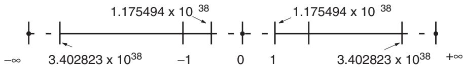
line
| x | y | | ------- | ----------- | | -∞ | - | | 3.402823 x 10^38 | 1.175494 x 10^38 | | -1 | - | | 0 | 1.175494 x 10^38 | | 1 | - | | 3.402823 x 10^38 | +∞ |Special Numbers
The formats for NaN, ± , and 0 are as follows:
NaN*: e = 255, f ≠ 0
$$ + \infty : \quad e = 2 5 5, f = 0, s = 0 $$
$$ - \infty : \quad e = 2 5 5, f = 0, s = 1 $$
0: e = 0
*NaN (not a number) is not a valid floating-point number. Executing floating-point calculation instructions will not result in NaN.
Writing Floating-point Data
When floating-point is specified for the data format in the I/O memory edit display in the CX-Programmer, standard decimal numbers input in the display are automatically converted to the floating-point format shown above (IEEE754-format) and written to I/O Memory. Data written in the IEEE754-format is automatically converted to standard decimal format when monitored on the display.
It isn't necessary for the user to be aware of the IEEE754 data format when reading and writing floating-point data. It is only necessary to remember that floating point values occupy two words each.
Numbers Expressed as Floating-point Values
The following types of floating-point numbers can be used.
| Mantissa (f) | Exponent (e) | ||
| 0 | Not 0 and not all 1's | All 1's (255) | |
| 0 | 0 | Normal number | Infinity |
| Not 0 | Non-normal number | NaN | |
Note A non-normal number is one whose absolute value is too small to be expressed as a normal number. Non-normal numbers have fewer significant digits. If the result of calculations is a non-normal number (including intermediate results), the number of significant digits will be reduced.
Normal Numbers
Normal numbers express real numbers. The sign bit will be 0 for a positive number and 1 for a negative number.
The exponent (e) will be expressed from 1 to 254, and the real exponent will be 127 less, i.e., -126 to 127.
The mantissa (f) will be expressed from 0 to 2^33 - 1 , and it is assume that, in the real mantissa, bit 2^33 is 1 and the binary point follows immediately after it.
Normal numbers are expressed as follows:
$$ (- 1) ^ {(\mathrm{signs})} \times 2 ^ {(\mathrm{exponente}) - 1 2 7} \times (1 + \mathrm{mantissa} \times 2 ^ {- 2 3}) $$
Example
$$ \boxed {1 \left| 1 0 0 0 0 0 0 0 0 \right| 1 1 0 0 0 0 0 0 0 0 0 0 0 0 0 0 0 0 0 0 0 0} $$
Sign: -
Exponent: 128 - 127 = 1
Mantissa: 1 + (2^22 + 2^21) × 2^-23 = 1 + (2^-1 + 2^-2) = 1 + 0.75 = 1.75
Value: -1.75 × 2^1 = -3.5
Non-normal Numbers
Non-normal numbers express real numbers with very small absolute values. The sign bit will be 0 for a positive number and 1 for a negative number.
The exponent (e) will be 0, and the real exponent will be -126.
The mantissa (f) will be expressed from 1 to 2^33 - 1 , and it is assume that, in the real mantissa, bit 2^33 is 0 and the binary point follows immediately after it.
Non-normal numbers are expressed as follows:
$$ (- 1) ^ {(\text { sign s })} \times 2 ^ {- 1 2 6} \times (\text { mantissa } \times 2 ^ {- 2 3}) $$
Example
$$ \boxed {0} \boxed {0} \boxed {0} \boxed {0} \boxed {0} \boxed {0} \boxed {0} \boxed {0} \boxed {0} \boxed {0} \boxed {1} \boxed {1} \boxed {0} \boxed {0} \boxed {0} \boxed {0} \boxed {0} \boxed {0} \boxed {0} \boxed {0} \boxed {0} \boxed {0} \boxed {0} \boxed {0} \boxed {0} \boxed {0} \boxed {0} $$
Sign: -
Exponent: -126
Mantissa: 0 + (2^22 + 2^21) × 2^-23 = 0 + (2^-1 + 2^-2) = 0 + 0.75 = 0.75
Value: -0.75 × 2^-126
Zero
Values of +0.0 and -0.0 can be expressed by setting the sign to 0 for positive or 1 for negative. The exponent and mantissa will both be 0. Both +0.0 and -0.0 are equivalent to 0.0. Refer to Floating-point Arithmetic Results, below, for differences produced by the sign of 0.0.
Infinity
Values of + and - can be expressed by setting the sign to 0 for positive or 1 for negative. The exponent will be 255 ( 2^8 - 1 ) and the mantissa will be 0.
NaN
NaN (not a number) is produced when the result of calculations, such as 0.0/0.0, / , or - , does not correspond to a number or infinity. The exponent will be 255(2^8-1) and the mantissa will be not 0.
Note There are no specifications for the sign of NaN or the value of the mantissa field (other than to be not 0).
Floating-point Arithmetic Results
| Rounding Results | The following methods will be used to round results when the number of digits in the accurate result of floating-point arithmetic exceeds the significant digits of internal processing expressions.If the result is close to one of two internal floating-point expressions, the closer expression will be used. If the result is midway between two internal floating-point expressions, the result will be rounded so that the last digit of the mantissa is 0. |
| Overflows, Underflows, and Illegal Calculations | Overflows will be output as either positive or negative infinity, depending on the sign of the result. Underflows will be output as either positive or negative zero, depending on the sign of the result.Illegal calculations will result in NaN. Illegal calculations include adding infinity to a number with the opposite sign, subtracting infinity from a number with the opposite sign, multiplying zero and infinity, dividing zero by zero, or dividing infinity by infinity.The value of the result may not be correct if an overflow occurs when converting a floating-point number to an integer. |
| Precautions in Handling Special Values | The following precautions apply to handling zero, infinity, and NaN.The sum of positive zero and negative zero is positive zero.The difference between zeros of the same sign is positive zero.If any operand is a NaN, the results will be a NaN.Positive zero and negative zero are treated as equivalent in comparisons.Comparison or equivalency tests on one or more NaN will always be true for != and always be false for all other instructions. |
Floating-point Calculation Results
| When the absolute value of the result is greater than the maximum value that can be expressed for floating-point data, the Overflow Flag (SR 25404) will turn ON and the result will be output as ± . If the result is positive, it will be output as + ; if negative, then - .The Equals Flag will only turn ON when both the exponent (e) and the mantissa (f) are zero after a calculation. A calculation result will also be output as zero when the absolute value of the result is less than the minimum value that can be expressed for floating-point data. In that case the Underflow Flag (SR 25405) will turn ON. | |
| Example | In this program example, the X-axis and Y-axis coordinates (x, y) are provided by 4-digit BCD content of DM 0000 and DM 0001. The distance (r) from the origin and the angle ( , in degrees) are found and output to DM 0100 and DM 0101. In the result, everything to the right of the decimal point is truncated. |
flowchart
graph TD
A["000000"] --> B["BIN"]
B --> C["DM 0000, DM 0200"]
A --> D["BIN"]
D --> E["DM 0001, DM 0201"]
A --> F["FLT"]
F --> G["DM 0200, DM 0202"]
A --> H["FLT"]
H --> I["DM 0201, DM 0204"]
A --> J["*F"]
J --> K["DM 0202, DM 0202, DM 0206"]
A --> L["*F"]
L --> M["DM 0204, DM 0204, DM 0208"]
A --> N["+F"]
N --> O["DM 0206, DM 0208, DM 0210"]
A --> P["SQRT"]
P --> Q["DM 0210, DM 0212"]
A --> R["/F"]
R --> S["DM 0204, DM 0202, DM 0214"]
A --> T["ATAN"]
T --> U["DM 0214, DM 0216"]
A --> V["DEG"]
V --> W["DM 0216, DM 0218"]
A --> X["FIX"]
X --> Y["DM 0212, DM 0220"]
A --> Z["FIX"]
Z --> AA["DM 0218, DM 0221"]
A --> AB["BCD"]
AB --> AC["DM 0220, DM 0100"]
A --> AD["BCD"]
AD --> AE["DM 0221, DM 0101"]
A --> AF["END"]
Calculations
$$ \text { Distance } r = \sqrt {x ^ {2} + y ^ {2}} $$
$$ \text { Angle } = \tan^ {- 1} \left(\frac {y}{x}\right) $$
Example
$$ \text { Distance } r = \sqrt {1 0 0 ^ {2} + 1 0 0 ^ {2}} = 1 4 1. 4 2 1 4 $$
$$ \text { Angle } = \tan^ {- 1} \left(\frac {1 0 0}{1 0 0}\right) = 4 5. 0 $$
DM Contents
$$ \begin{array}{l} \begin{array}{c c c} \text {DM 0000} \boxed {0 1 0 0} & x \ (\text {BCD}) & \longrightarrow \end{array} \quad \begin{array}{c c c} \text {DM 0100} \boxed {0 1 4 1} & r \ \hline \end{array} \ \begin{array}{c} \text {DM 0001} \boxed {0 1 0 0} \ (\text {BCD}) \end{array} \quad \text {y} \quad \text {DM 0101} \boxed {0 0 4 5} \quad \theta \ \end{array} $$
- This section of the program converts the data from BCD to floating-point.
a) The data area from DM 0200 onwards is used as a work area.
b) First BIN(23) is used to temporarily convert the BCD data to binary data, and then FLT(—) is used to convert the binary data to floating-point data.
c) The value of x that has been converted to floating-point data is output to DM 0203 and DM 0202.
d) The value of y that has been converted to floating-point data is output to DM 0205 and DM 0204.
- In order to find the distance r, Floating-point Math Instructions are used to calculate the square root of x^2+y^2 . The result is then output to DM 0213 and DM 0212 as floating-point data.
- In order to find the angle , Floating-point Math Instructions are used to calculate ^-1(y/x) . ATAN(—) outputs the result in radians, so DEG(—) is used to convert to degrees. The result is then output to DM 0219 and DM 0218 as floating-point data.
- The data is converted back from floating-point to BCD.
a) First FIX(—) is used to temporarily convert the floating-point data to binary data, and then BCD(024) is used to convert the binary data to BCD data.
b) The distance r is output to DM 0100.
c) The angle is output to DM 0101.
5-24-1 FLOATING TO 16-BIT: FIX(—)
Operand Data Areas
| Ladder Symbols | |
| FIX(—) | @FIX(—) |
| S | S |
| R | R |
| 000 | 000 |
Limitations
The content of S+1 and S must be floating-point data and the integer portion must be in the range of -32,768 to 32,767.
DM 6144 to DM 6655 cannot be used for R.
Description
When the execution condition is OFF, FIX(—) is not executed. When the execution condition is ON, FIX(—) converts the integer portion of the 32-bit floating-point number in S+1 and S (IEEE754-format) to 16-bit signed binary data and places the result in R.
flowchart
graph TD
A["S+1"] --> B["S"]
B --> C["R"]
Floating-point data (32 bits)
Signed binary data (16 bits)
Only the integer portion of the floating-point data is converted, and the fraction portion is truncated. The integer portion of the floating-point data must be within the range of -32,768 to 32,767.
Example conversions:
A floating-point value of 3.5 is converted to 3.
A floating-point value of -3.5 is converted to -3.
Flags
ER: Indirectly addressed EM/DM word is non-existent.
(Content of *EM/*DM word is not BCD, or the EM/DM area boundary has been exceeded.)
ON if the data in S+1 and S is not a number (NaN).
ON if the integer portion of S+1 and S is not within the range of -32,768 to 32,767.
EQ: ON if the result is 0000.
5-24-2 FLOATING TO 32-BIT: FIXL(—)
Ladder Symbols
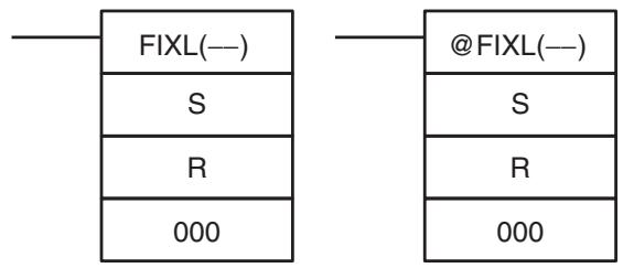
Operand Data Areas
| S: First source word |
| IR, SR, AR, DM, EM, HR, TIM/CNT, LR |
| R: First result word |
| IR, SR, AR, DM, EM, HR, LR |
| Third operand: Always 000 |
| ---- |
Limitations
The content of S+1 and S must be floating-point data and the integer portion must be in the range of -2,147,483,648 to 2,147,483,647.
DM 6143 to DM 6655 cannot be used for R.
Description
When the execution condition is OFF, FIXL(—) is not executed. When the execution condition is ON, FIXL(—) converts the integer portion of the 32-bit floating-point number in S+1 and S (IEEE754-format) to 32-bit signed binary data and places the result in R+1 and R.
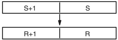
flowchart
graph TD
A["S+1"] --> B["R+1"]
C["S"] --> D["R"]
Floating-point data (32 bits)
Signed binary data (32 bits)
Only the integer portion of the floating-point data is converted, and the fraction portion is truncated. (The integer portion of the floating-point data must be within the range of -2,147,483,648 to 2,147,483,647.)
Example conversions:
A floating-point value of 2,147,483,640.5 is converted to 2,147,483,640.
A floating-point value of -2,147,483,640.5 is converted to -2,147,483,640.
Flags
ER: Indirectly addressed EM/DM word is non-existent.
(Content of *EM/*DM word is not BCD, or the EM/DM area boundary has been exceeded.)
ON if the data in S+1 and S is not a number (NaN).
ON if the integer portion of S+1 and S is not within the range of -2,147,483,648 to 2,147,483,647.
EQ: ON if the result is 0000 0000.
5-24-3 16-BIT TO FLOATING: FLT(—)
Ladder Symbols
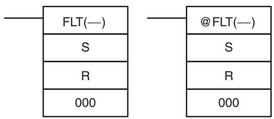
Operand Data Areas
| S: Source word |
| IR, SR, AR, DM, EM, HR, TIM/CNT, LR, # |
R: First result word
IR, SR, AR, DM, EM, HR, LR
Third operand: Always 000
Limitations
The content of S must contain signed binary data with a (decimal) value in the range of -32,768 to 32,767.
DM 6143 to DM 6655 cannot be used for R.
Description
When the execution condition is OFF, FLT(—) is not executed. When the execution condition is ON, FLT(—) converts the 16-bit signed binary value in S to 32-bit floating-point data (IEEE754-format) and places the result in R+1 and R. A single 0 is added after the decimal point in the floating-point result.
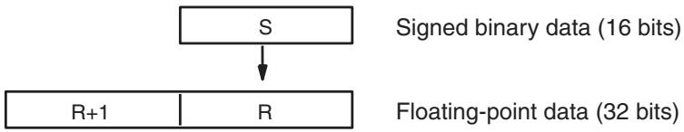
flowchart
graph TD
A["S"] --> B["R+1"]
A --> C["R"]
D["Signed binary data (16 bits)"] --> E["Floating-point data (32 bits)"]
Only values within the range of -32,768 to 32,767 can be specified for S. To convert signed binary data outside of that range, use FLTL(—).
Example conversions:
A signed binary value of 3 is converted to 3.0.
A signed binary value of -3 is converted to -3.0.
Flags
ER: Indirectly addressed EM/DM word is non-existent.
(Content of *EM/*DM word is not BCD, or the EM/DM area boundary has been exceeded.)
EQ: ON if both the exponent and mantissa of the result are 0.
5-24-4 32-BIT TO FLOATING: FLTL(—)
Ladder Symbols
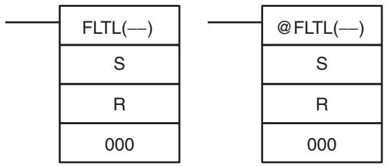
Operand Data Areas
| S: First source word |
| IR, SR, AR, DM, EM, HR, TIM/CNT, LR |
| R: First result word |
| IR, SR, AR, DM, EM, HR, LR |
| Third operand: Always 000 |
| — |
Limitations
The result will not be exact if a number with an absolute value greater than 16,777,215 (the maximum value that can be expressed in 24-bits) is converted.
DM 6143 to DM 6655 cannot be used for R.
Description
When the execution condition is OFF, FLTL(—) is not executed. When the execution condition is ON, FLTL(—) converts the 32-bit signed binary value in S+1 and S to 32-bit floating-point data (IEEE754-format) and places the result in R+1 and R. A single 0 is added after the decimal point in the floating-point result.
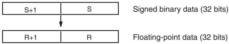
flowchart
graph TD
A["S+1"] --> B["R+1"]
C["S"] --> B
D["Signed binary data (32 bits)"] --> E["Floating-point data (32 bits)"]
Signed binary data within the range of -2,147,483,648 to 2,147,483,647 can be specified for S+1 and S. The floating point value has 24 significant binary digits (bits). The result will not be exact if a number greater than 16,777,215 (the maximum value that can be expressed in 24-bits) is converted by FLTL(—).
Example Conversions:
A signed binary value of 16,777,215 is converted to 16,777,215.0.
A signed binary value of -16,777,215 is converted to -16,777,215.0.
Flags
ER: Indirectly addressed EM/DM word is non-existent.
(Content of *EM/*DM word is not BCD, or the EM/DM area boundary has been exceeded.)
EQ: ON if both the exponent and mantissa of the result are 0.
5-24-5 FLOATING-POINT ADD: +F(—)
Ladder Symbols
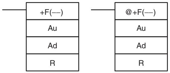
Operand Data Areas
| Au: First augend word |
| IR, SR, AR, DM, EM, HR, TIM/CNT, LR |
| Ad: First addend word |
| IR, SR, AR, DM, EM, HR, TIM/CNT, LR |
| R: First result word |
| IR, SR, AR, DM, EM, HR, LR |
Limitations
The augend (Au+1 and Au) and Addend (Ad+1 and Ad) data must be in IEEE754 floating-point data format.
DM 6143 to DM 6655 cannot be used for R.
Description
When the execution condition is OFF, +F(—) is not executed. When the execution condition is ON, +F(—) adds the 32-bit floating-point number in Ad+1 and Ad to the 32-bit floating-point number in Au+1 and Au and places the result in R+1 and R. (The floating point data must be in IEEE754 format.)
| Au+1 | Au |
| + | Ad+1 | Ad |
Augend (floating-point data, 32 bits)
Addend (floating-point data, 32 bits)
| R+1 | R |
Result (floating-point data, 32 bits)
If the absolute value of the result is greater than the maximum value that can be expressed as floating-point data, the Overflow Flag (SR 25404) will turn ON and the result will be output as ± .
If the absolute value of the result is less than the minimum value that can be expressed as floating-point data, the Underflow Flag (SR 25405) will turn ON and the result will be output as 0.
The various combinations of augend and addend data will produce the results shown in the following table.
| Augend | |||||
| Addend | 0 | Numeral | + | - | NaN |
| 0 | 0 | Numeral | + | - | See note 2. |
| Numeral | Numeral | See note 1. | + | - | |
| + | + | + | + | See note 2. | |
| - | - | - | See note 2. | - | |
| NaN | See note 2. | ||||
Note
- The results could be zero (including underflows), a numeral, + , or - .
- The Error Flag will be turned ON and the instruction won't be executed.
Flags
ER: Indirectly addressed EM/DM word is non-existent.
(Content of *EM/*DM word is not BCD, or the EM/DM area boundary has been exceeded.)
ON if the augend or addend data is not recognized as floating-point data.
EQ: ON if both the exponent and mantissa of the result are 0.
OF: ON if the absolute value of the result is too large to be expressed as a 32-bit floating-point value. (The result will be output as ± .)
UF: ON if the absolute value of the result is too small to be expressed as a 32-bit floating-point value. (The result will be output as 0.)
5-24-6 FLOATING-POINT SUBTRACT: -F(—)
Ladder Symbols

flowchart
graph TD
A["F(—)"] --> B["Mi"]
A --> C["Su"]
A --> D["R"]
E["@ F(—)"] --> F["Mi"]
E --> G["Su"]
E --> H["R"]
Operand Data Areas
| Mi: First minuend word |
| IR, SR, AR, DM, EM, HR, TIM/CNT, LR |
| Su: First subtrahend word |
| IR, SR, AR, DM, EM, HR, TIM/CNT, LR |
| R: First result word |
| IR, SR, AR, DM, EM, HR, LR |
Limitations
The Minuend (Mi+1 and Mi) and Subtrahend (Su+1 and Su) data must be in IEEE754 floating-point data format.
DM 6143 to DM 6655 cannot be used for R.
Description
When the execution condition is OFF, -F(—) is not executed. When the execution condition is ON, -F(—) subtracts the 32-bit floating-point number in Su+1 and Su from the 32-bit floating-point number in Mi+1 and Mi and places the result in R+1 and R. (The floating point data must be in IEEE754 format.)
| Mi+1 | Mi |
Minuend (floating-point data, 32 bits)
| — | Su+1 | Su |
Subtrahend (floating-point data, 32 bits)
| R+1 | R |
Result (floating-point data, 32 bits)
If the absolute value of the result is greater than the maximum value that can be expressed as floating-point data, the Overflow Flag (SR 25404) will turn ON and the result will be output as ± .
If the absolute value of the result is less than the minimum value that can be expressed as floating-point data, the Underflow Flag (SR 25405) will turn ON and the result will be output as 0.
The various combinations of minuend and subtrahend data will produce the results shown in the following table.
| Minuend | |||||
| Subtrahend | 0 | Numeral | + | - | NaN |
| 0 | 0 | Numeral | + | - | |
| Numeral | Numeral | See note 1. | + | - | |
| + | - | - | See note 2. | - | |
| - | + | + | + | See note 2. | |
| NaN | See note 2. | ||||
Note
- The results could be zero (including underflows), a numeral, + , or - .
- The Error Flag will be turned ON and the instruction won't be executed.
Flags
ER: Indirectly addressed EM/DM word is non-existent.
(Content of *EM/*DM word is not BCD, or the EM/DM area boundary has been exceeded.)
ON if the minuend or subtrahend data is not recognized as floating-point data.
EQ: ON if both the exponent and mantissa of the result are 0.
OF: ON if the absolute value of the result is too large to be expressed as a 32-bit floating-point value. (The result will be output as ± .)
UF: ON if the absolute value of the result is too small to be expressed as a 32-bit floating-point value. (The result will be output as 0.)
5-24-7 FLOATING-POINT MULTIPLY: \*F(—)
Ladder Symbols
| Md: First multiplicand word |
| IR, SR, AR, DM, EM, HR, TIM/CNT, LR |
Mr: First multiplier word
| IR, SR, AR, DM, EM, HR, TIM/CNT, LR |
R: First result word
| IR, SR, AR, DM, EM, HR, LR |
Limitations
The Multiplicand (Md+1 and Md) and Multiplier (Mr+1 and Mr) data must be in IEEE754 floating-point data format.
DM 6143 to DM 6655 cannot be used for R.
Description
When the execution condition is OFF, F(—) is not executed. When the execution condition is ON, F(—) multiplies the 32-bit floating-point number in Md+1 and Md by the 32-bit floating-point number in Mr+1 and Mr and places the result in R+1 and R. (The floating point data must be in IEEE754 format.)
| Md+1 | Md |
Multiplicand (floating-point data, 32 bits)
| × | Mr+1 | Mr |
Multiplier (floating-point data, 32 bits)
| R+1 | R |
Result (floating-point data, 32 bits)
If the absolute value of the result is greater than the maximum value that can be expressed as floating-point data, the Overflow Flag (SR 25404) will turn ON and the result will be output as ± .
If the absolute value of the result is less than the minimum value that can be expressed as floating-point data, the Underflow Flag (SR 25405) will turn ON and the result will be output as 0.
The various combinations of multiplicand and multiplier data will produce the results shown in the following table.
| Multiplicand | |||||
| Multiplier | 0 | Numeral | + | - | NaN |
| 0 | 0 | 0 | See note 2. | See note 2. | See note 2. |
| Numeral | 0 | See note 1. | +/- | +/- | |
| + | See note 2. | +/- | + | - | |
| - | See note 2. | +/- | - | + | |
| NaN | See note 2. | ||||
Note
- The results could be zero (including underflows), a numeral, + , or - .
- The Error Flag will be turned ON and the instruction won't be executed.
Flags
ER: Indirectly addressed EM/DM word is non-existent.
(Content of *EM/*DM word is not BCD, or the EM/DM area boundary has been exceeded.)
ON if the multiplicand or multiplier data is not recognized as floating-point data.
EQ: ON if both the exponent and mantissa of the result are 0.
OF: ON if the absolute value of the result is too large to be expressed as a 32-bit floating-point value. (The result will be output as ± .)
UF: ON if the absolute value of the result is too small to be expressed as a 32-bit floating-point value. (The result will be output as 0.)
5-24-8 FLOATING-POINT DIVIDE: /F(—)
Operand Data Areas
| Ladder Symbols | |
| /F(—) | @/F(—) |
| Dd | Dd |
| Dr | Dr |
| R | R |
| Dd: First dividend word |
| IR, SR, AR, DM, EM, HR, TIM/CNT, LR |
| Dr: First divisor word |
| IR, SR, AR, DM, EM, HR, TIM/CNT, LR |
| R: First result word |
| IR, SR, AR, DM, EM, HR, LR |
Limitations
The Dividend (Dd+1 and Dd) and Divisor (Dr+1 and Dr) data must be in IEEE754 floating-point data format.
DM 6143 to DM 6655 cannot be used for R.
Description
When the execution condition is OFF, /F(—) is not executed. When the execution condition is ON, /F(—) divides the 32-bit floating-point number in Dd+1 and Dd by the 32-bit floating-point number in Dr+1 and Dr and places the result in R+1 and R. (The floating point data must be in IEEE754 format.)
| Dd+1 | Dd |
| Dr+1 | Dr |
| R+1 | R |
Dividend (floating-point data, 32 bits)
Divisor (floating-point data, 32 bits)
If the absolute value of the result is greater than the maximum value that can be expressed as floating-point data, the Overflow Flag (SR 25404) will turn ON and the result will be output as ± .
If the absolute value of the result is less than the minimum value that can be expressed as floating-point data, the Underflow Flag (SR 25405) will turn ON and the result will be output as 0.
The various combinations of dividend and divisor data will produce the results shown in the following table.
| Dividend | |||||
| Divisor | 0 | Numeral | + | - | NaN |
| 0 | See note 3. | +/- | + | - | |
| Numeral | 0 | See note 1. | +/- | +/- | |
| + | 0 | See note 2. | See note 3. | See note 3. | |
| - | 0 | See note 2. | See note 3. | See note 3. | |
| NaN | See note 3. | ||||
Note
- The results could be zero (including underflows), a numeral, + , or - .
- The results will be zero for underflows.
- The Error Flag will be turned ON and the instruction won't be executed.
Flags
ER: Indirectly addressed EM/DM word is non-existent.
(Content of *EM/*DM word is not BCD, or the EM/DM area boundary has been exceeded.)
ON if the dividend or divisor data is not recognized as floating-point data.
EQ: ON if both the exponent and mantissa of the result are 0.
OF: ON if the absolute value of the result is too large to be expressed as a 32-bit floating-point value. (The result will be output as ± .)
UF: ON if the absolute value of the result is too small to be expressed as a 32-bit floating-point value. (The result will be output as 0.)
5-24-9 DEGREES TO RADIANS: RAD(—)
Ladder Symbols
| RAD(—) | @RAD(—) |
| S | S |
| R | R |
| 000 | 000 |
Operand Data Areas
| S: First source word |
| IR, SR, AR, DM, EM, HR, TIM/CNT, LR |
| R: First result word |
| IR, SR, AR, DM, EM, HR, LR |
| Third operand: Always 000 |
| — |
Limitations
The source data in S+1 and S must be in IEEE754 floating-point data format.
DM 6143 to DM 6655 cannot be used for R.
Description
When the execution condition is OFF, RAD(—) is not executed. When the execution condition is ON, RAD(—) converts the 32-bit floating-point number in S+1 and S from degrees to radians and places the result in R and R+1. (The floating point source data must be in IEEE754 format.)
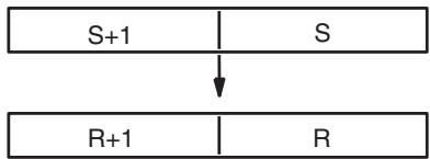
flowchart
graph TD
A["S+1"] --> B["R+1"]
C["S"] --> D["R"]
Source (degrees, 32-bit floating-point data)
Result (radians, 32-bit floating-point data)
Degrees are converted to radians by means of the following formula:
Degrees × π/180 = radians
If the absolute value of the result is greater than the maximum value that can be expressed as floating-point data, the Overflow Flag (SR 25404) will turn ON and the result will be output as ± .
If the absolute value of the result is less than the minimum value that can be expressed as floating-point data, the Underflow Flag (SR 25405) will turn ON and the result will be output as 0.
Flags
ER: Indirectly addressed EM/DM word is non-existent.
(Content of *EM/*DM word is not BCD, or the EM/DM area boundary has been exceeded.)
ON if the source data is not recognized as floating-point data.
EQ: ON if both the exponent and mantissa of the result are 0.
OF: ON if the absolute value of the result is too large to be expressed as a 32-bit floating-point value. (The result will be output as ± .)
UF: ON if the absolute value of the result is too small to be expressed as a 32-bit floating-point value. (The result will be output as 0.)
5-24-10 RADIANS TO DEGREES: DEG(—)
Ladder Symbols
| S: First source word |
| IR, SR, AR, DM, EM, HR, TIM/CNT, LR |
| R: First result word |
| IR, SR, AR, DM, EM, HR, LR |
| Third operand: Always 000 |
| — |
Limitations
The source data in S+1 and S must be in IEEE754 floating-point data format. DM 6143 to DM 6655 cannot be used for R.
Description
When the execution condition is OFF, DEG(—) is not executed. When the execution condition is ON, DEG(—) converts the 32-bit floating-point number in S+1 and S from radians to degrees and places the result in R+1 and R. (The floating point source data must be in IEEE754 format.)
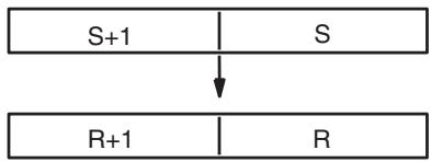
flowchart
graph TD
A["S+1"] --> B["S"]
B --> C["R+1"]
C --> D["R"]
Source (radians, 32-bit floating-point data)
Result (degrees, 32-bit floating-point data)
Radians are converted to degrees by means of the following formula:
Radians × 180/π = degrees
If the absolute value of the result is greater than the maximum value that can be expressed as floating-point data, the Overflow Flag (SR 25404) will turn ON and the result will be output as ± .
If the absolute value of the result is less than the minimum value that can be expressed as floating-point data, the Underflow Flag (SR 25405) will turn ON and the result will be output as 0.
Flags
ER: Indirectly addressed EM/DM word is non-existent.
(Content of *EM/*DM word is not BCD, or the EM/DM area boundary has been exceeded.)
ON if the source data is not recognized as floating-point data.
EQ: ON if both the exponent and mantissa of the result are 0.
OF: ON if the absolute value of the result is too large to be expressed as a 32-bit floating-point value. (The result will be output as ± .)
UF: ON if the absolute value of the result is too small to be expressed as a 32-bit floating-point value. (The result will be output as 0.)
5-24-11 SINE: SIN(—)
Ladder Symbols
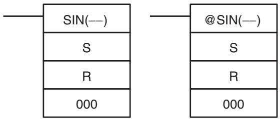
| S: First source word |
| IR, SR, AR, DM, EM, HR, TIM/CNT, LR |
| R: First result word |
| IR, SR, AR, DM, EM, HR, LR |
| Third operand: Always 000 |
| --- |
Limitations
The source data in S+1 and S must be in IEEE754 floating-point data format.
DM 6143 to DM 6655 cannot be used for R.
Description
When the execution condition is OFF, SIN(—) is not executed. When the execution condition is ON, SIN(—) calculates the sine of the angle (in radians) expressed as a 32-bit floating-point value in S+1 and S and places the result in R+1 and R. (The floating point source data must be in IEEE754 format.)
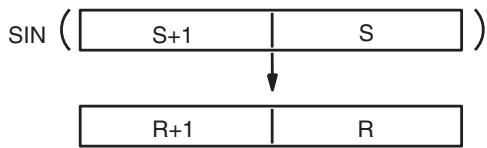
flowchart
graph TD
A["SIN (S+1)"] --> C["R+1"]
B["S"] --> C["R+1"]
Source (32-bit floating-point data)
Result (32-bit floating-point data)
Specify the desired angle (−65,535 to 65,535) in radians in S+1 and S. If the absolute value of the angle exceeds 65,535, an error will occur and the instruction won't be executed. For information on converting from degrees to radians, see 5-24-9 DEGREES TO RADIANS: RAD(—).
The following diagram shows the relationship between the angle and result.
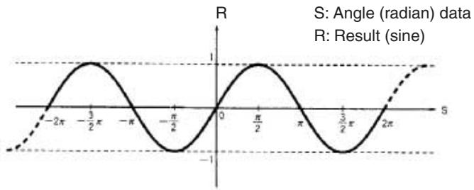
line
| x | y | | ------- | ----- | | -2π | -0.5 | | -π/2 | 1.0 | | -π | -0.5 | | 0 | 1.0 | | π/2 | -0.5 | | π | 1.0 | | 3π/2 | -0.5 | | 2π | 1.0 |Flags
ER: Indirectly addressed EM/DM word is non-existent.
(Content of *EM/*DM word is not BCD, or the EM/DM area boundary has been exceeded.)
ON if the source data is not recognized as floating-point data.
ON if the absolute value of the source data exceeds 65,535.
EQ: ON if both the exponent and mantissa of the result are 0.
5-24-12 COSINE: COS(—)
Operand Data Areas
| Ladder Symbols | |
| COS(—) | @COS(—) |
| S | S |
| R | R |
| 000 | 000 |
| S: First source word |
| IR, SR, AR, DM, EM, HR, TIM/CNT, LR |
| R: First result word |
| IR, SR, AR, DM, EM, HR, LR |
| Third operand: Always 000 |
| —— |
Limitations
The source data in S+1 and S must be in IEEE754 floating-point data format.
DM 6143 to DM 6655 cannot be used for R.
Description
When the execution condition is OFF, COS(—) is not executed. When the execution condition is ON, COS(—) calculates the cosine of the angle (in radians) expressed as a 32-bit floating-point value in S+1 and S and places the result in R+1 and R. (The floating point source data must be in IEEE754 format.)
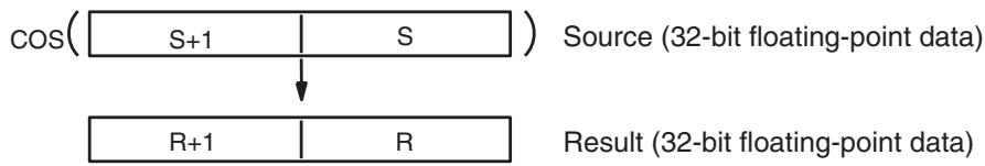
flowchart
graph TD
A["Source (32-bit floating-point data)"] --> B["Result (32-bit floating-point data)"]
C["COS(S+1) S"] --> D["R+1 R"]
D --> E["Output"]
Specify the desired angle (−65,535 to 65,535) in radians in S+1 and S. If the absolute value of the angle exceeds 65,535, an error will occur and the instruction won't be executed. For information on converting from degrees to radians, see 5-24-9 DEGREES TO RADIANS: RAD(—).
The following diagram shows the relationship between the angle and result.
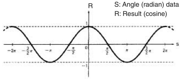
line
| x | y | | ------- | ----- | | -2π | 1 | | -π/2 | 0 | | 0 | 1 | | π/2 | 0 | | π | -1 | | 3π/2 | 0 | | 2π | 1 |Flags
ER: Indirectly addressed EM/DM word is non-existent.
(Content of *EM/*DM word is not BCD, or the EM/DM area boundary has been exceeded.)
ON if the source data is not recognized as floating-point data.
ON if the absolute value of the source data exceeds 65,535.
EQ: ON if both the exponent and mantissa of the result are 0.
5-24-13 TANGENT: TAN(—)
Ladder Symbols
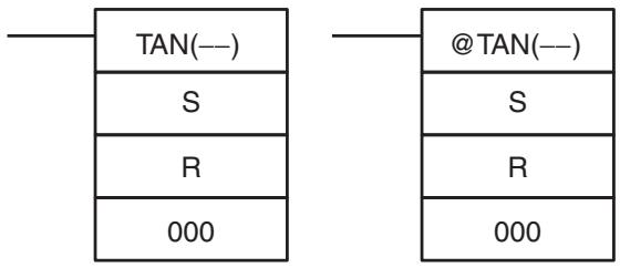
| S: First source word |
| IR, SR, AR, DM, EM, HR, TIM/CNT, LR |
| R: First result word |
| IR, SR, AR, DM, EM, HR, LR |
| Third operand: Always 000 |
| —— |
Limitations
The source data in S+1 and S must be in IEEE754 floating-point data format. DM 6143 to DM 6655 cannot be used for R.
Description
When the execution condition is OFF, TAN(—) is not executed. When the execution condition is ON, TAN(—) calculates the tangent of the angle (in radians) expressed as a 32-bit floating-point value in S+1 and S and places the result in R+1 and R. (The floating point source data must be in IEEE754 format.)

flowchart
graph TD
A["TAN (S+1 | S)"] --> B["Result (32-bit floating-point data)"]
B --> C["R+1 | R"]
Specify the desired angle (−65,535 to 65,535) in radians in S+1 and S. If the absolute value of the angle exceeds 65,535, an error will occur and the instruction won't be executed. For information on converting from degrees to radians, see 5-24-9 DEGREES TO RADIANS: RAD(—).
If the absolute value of the result is greater than the maximum value that can be expressed as floating-point data, the Overflow Flag (SR 25404) will turn ON and the result will be output as ± .
The following diagram shows the relationship between the angle and result.
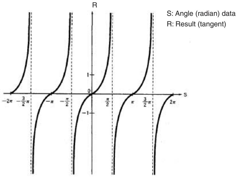
line
| S | R (Angle) | R (Tangent) | | --------- | --------- | ----------- | | -2π | 0 | 0 | | -π/2 | 0 | 0 | | π | 0 | 0 | | 3π/2 | 0 | 0 | | 2π | 0 | 0 |Flags
ER: Indirectly addressed EM/DM word is non-existent.
(Content of *EM/*DM word is not BCD, or the EM/DM area boundary has been exceeded.)
ON if the source data is not recognized as floating-point data.
ON if the absolute value of the source data exceeds 65,535.
EQ: ON if both the exponent and mantissa of the result are 0.
5-24-14 ARC SINE: ASIN(—)
Operand Data Areas
The source data in S+1 and S must be in IEEE754 floating-point data format.
DM 6143 to DM 6655 cannot be used for R.
Description
ASIN(—) calculates the arc sine of a 32-bit floating-point number and places the result in the specified result words. (The arc sine function is the inverse of the sine function; it returns the angle that produces a given sine value between -1 and 1.)
When the execution condition is OFF, ASIN(—) is not executed. When the execution condition is ON, ASIN(—) computes the angle (in radians) for a sine value expressed as a 32-bit floating-point number in S+1 and S and places the result in R+1 and R. (The floating point source data must be in IEEE754 format.)
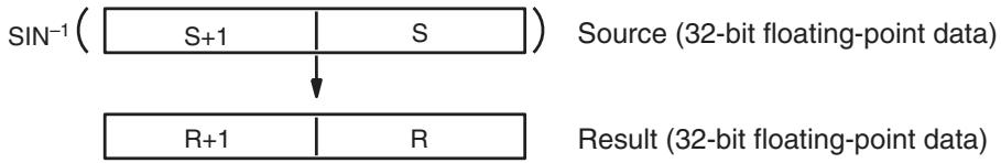
flowchart
graph TD
A["SIN⁻¹"] --> B["Source (32-bit floating-point data)"]
A --> C["R+1"]
C --> D["Result (32-bit floating-point data)"]
The source data must be between -1.0 and 1.0. If the absolute value of the source data exceeds 1.0, an error will occur and the instruction won't be executed.
The result is output to words R+1 and R as an angle (in radians) within the range of -/2 to /2 .
The following diagram shows the relationship between the input data and result.
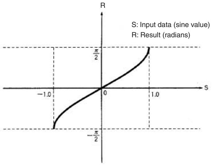
line
| S | R | |-------|---------| | -1.0 | -π/2 | | 0 | 0 | | 1.0 | π/2 |Flags
ER: Indirectly addressed EM/DM word is non-existent.
(Content of *EM/*DM word is not BCD, or the EM/DM area boundary has been exceeded.)
ON if the source data is not recognized as floating-point data.
ON if the absolute value of the source data exceeds 1.0.
EQ: ON if both the exponent and mantissa of the result are 0.
5-24-15 ARC COSINE: ACOS(—)
Ladder Symbols
| S: First source word |
| IR, SR, AR, DM, EM, HR, TIM/CNT, LR |
| R: First result word |
| IR, SR, AR, DM, EM, HR, LR |
| Third operand: Always 000 |
| — |
Limitations
The source data in S+1 and S must be in IEEE754 floating-point data format.
DM 6143 to DM 6655 cannot be used for R.
Description
ACOS(—) calculates the arc cosine of a 32-bit floating-point number and places the result in the specified result words. (The arc cosine function is the inverse of the cosine function; it returns the angle that produces a given cosine value between -1 and 1.)
When the execution condition is OFF, ACOS(—) is not executed. When the execution condition is ON, ACOS(—) computes the angle (in radians) for a cosine value expressed as a 32-bit floating-point number in S+1 and S and places the result in R+1 and R. (The floating point source data must be in IEEE754 format.)
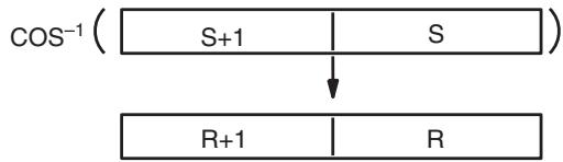
flowchart
graph TD
A["COS⁻¹"] --> B["S+1"]
A --> C["S"]
B --> D["R+1"]
C --> E["R"]
Source (32-bit floating-point data)
Result (32-bit floating-point data)
The source data must be between -1.0 and 1.0. If the absolute value of the source data exceeds 1.0, an error will occur and the instruction won't be executed.
The result is output to words R+1 and R as an angle (in radians) within the range of 0 to .
The following diagram shows the relationship between the input data and result.
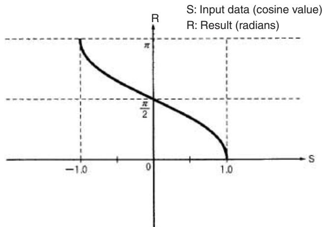
line
| S | R (cosine value) | |-------|------------------| | -1.0 | π | | 0 | π/2 | | 1.0 | 0 |Flags
ER: Indirectly addressed EM/DM word is non-existent.
(Content of *EM/*DM word is not BCD, or the EM/DM area boundary has been exceeded.)
ON if the source data is not recognized as floating-point data.
ON if the absolute value of the source data exceeds 1.0.
EQ: ON if both the exponent and mantissa of the result are 0.
5-24-16 ARC TANGENT: ATAN(—)
Ladder Symbols
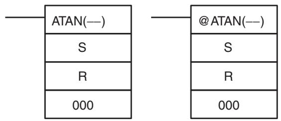
Operand Data Areas
| S: First source word |
| IR, SR, AR, DM, EM, HR, TIM/CNT, LR |
| R: First result word |
| IR, SR, AR, DM, EM, HR, LR |
| Third operand: Always 000 |
| — |
Limitations
The source data in S+1 and S must be in IEEE754 floating-point data format.
DM 6143 to DM 6655 cannot be used for R.
Description
ATAN(—) calculates the arc tangent of a 32-bit floating-point number and places the result in the specified result words. (The arc tangent function is the inverse of the tangent function; it returns the angle that produces a given tangent value.)
When the execution condition is OFF, ATAN(—) is not executed. When the execution condition is ON, ATAN(—) computes the angle (in radians) for a tangent value expressed as a 32-bit floating-point number in S+1 and S and places the result in R+1 and R. (The floating point source data must be in IEEE754 format.)
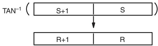
flowchart
graph TD
A["TAN⁻¹"] --> B["S+1"]
A --> C["S"]
B --> D["R+1"]
C --> E["R"]
Source (32-bit floating-point data)
Result (32-bit floating-point data)
The result is output to words R+1 and R as an angle (in radians) within the range of -/2 to /2 .
The following diagram shows the relationship between the input data and result.
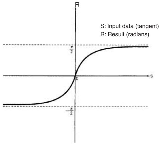
line
| S | R (radians) | |-------|-------------| | -π/2 | -π/2 | | 0 | 0 | | π/2 | π/2 |Flags
ER: Indirectly addressed EM/DM word is non-existent. (Content of *EM/*DM word is not BCD, or the EM/DM area boundary has been exceeded.) ON if the source data is not recognized as floating-point data.
EQ: ON if both the exponent and mantissa of the result are 0.
5-24-17 SQUARE ROOT: SQRT(—)
Ladder Symbols
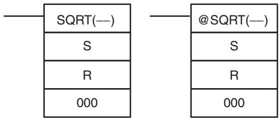
Operand Data Areas
| S: First source word |
| IR, SR, AR, DM, EM, HR, TIM/CNT, LR |
| R: First result word |
| IR, SR, AR, DM, EM, HR, LR |
| Third operand: Always 000 |
| — |
Limitations
The source data in S+1 and S must be in IEEE754 floating-point data format. DM 6143 to DM 6655 cannot be used for R.
Description
When the execution condition is OFF, SQRT(—) is not executed. When the execution condition is ON, SQRT(—) calculates the square root of the 32-bit floating-point number in S+1 and S and places the result in R+1 and R. (The floating point source data must be in IEEE754 format.)
flowchart
graph TD
A["S+1"] --> B["R+1"]
C["S"] --> D["R"]
Source (32-bit floating-point data)
Result (32-bit floating-point data)
The source data must be positive; if it is negative, an error will occur and the instruction won't be executed.
If the absolute value of the result is greater than the maximum value that can be expressed as floating-point data, the Overflow Flag (SR 25404) will turn ON and the result will be output as + .
The following diagram shows the relationship between the input data and result.
line
| S | R | | --- | --- | | 0 | 0 | | 1 | 1 | | 2 | 2 | | 3 | 2.5 | | 4 | 3 |Flags
ER: Indirectly addressed EM/DM word is non-existent.
(Content of *EM/*DM word is not BCD, or the EM/DM area boundary has been exceeded.)
ON if the source data is not recognized as floating-point data.
ON if the source data is negative.
EQ: ON if both the exponent and mantissa of the result are 0.
OF: ON if the absolute value of the result is too large to be expressed as a 32-bit floating-point value. (The result will be output as +∞.)
5-24-18 EXPONENT: EXP(—)
Ladder Symbols
flowchart
graph TD
A["EXP(--)"] --> B["S"]
A --> C["R"]
A --> D["000"]
E["@EXP(--)"] --> F["S"]
E --> G["R"]
E --> H["000"]
Operand Data Areas
| S: First source word |
| IR, SR, AR, DM, EM, HR, TIM/CNT, LR |
| R: First result word |
| IR, SR, AR, DM, EM, HR, LR |
| Third operand: Always 000 |
| —— |
Limitations
The source data in S+1 and S must be in IEEE754 floating-point data format.
DM 6143 to DM 6655 cannot be used for R.
Description
When the execution condition is OFF, EXP(—) is not executed. When the execution condition is ON, EXP(—) calculates the natural (base e) exponential of the 32-bit floating-point number in S+1 and S and places the result in R+1 and R. In other words, EXP(—) calculates e^x (x = source) and places the result in R+1 and R.
flowchart
graph TD
A["S+1"] --> B["e"]
C["R+1"] --> D["R"]
Source (32-bit floating-point data)
Result (32-bit floating-point data)
If the absolute value of the result is greater than the maximum value that can be expressed as floating-point data, the Overflow Flag (SR 25404) will turn ON and the result will be output as + .
If the absolute value of the result is less than the minimum value that can be expressed as floating-point data, the Underflow Flag (SR 25405) will turn ON and the result will be output as 0.
Note The constant e is 2.718282.
The following diagram shows the relationship between the input data and result.
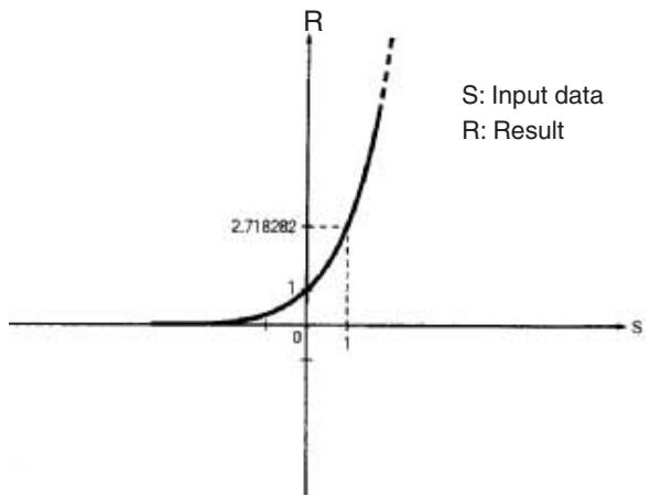
line
| S | R | | ------- | -------- | | 0 | 0 | | 1 | 2.718282 | | >1 | >2.718282 |Flags
ER: Indirectly addressed EM/DM word is non-existent.
(Content of *EM/*DM word is not BCD, or the EM/DM area boundary has been exceeded.)
ON if the source data is not recognized as floating-point data.
EQ: ON if both the exponent and mantissa of the result are 0.
OF: ON if the absolute value of the result is too large to be expressed as a 32-bit floating-point value. (The result will be output as +∞.)
UF: ON if the absolute value of the result is too small to be expressed as a 32-bit floating-point value. (The result will be output as 0.)
5-24-19 LOGARITHM: LOG(—)
Ladder Symbols
| LOG(—) | @LOG(—) |
| S | S |
| R | R |
| 000 | 000 |
Operand Data Areas
| S: First source word |
| IR, SR, AR, DM, EM, HR, TIM/CNT, LR |
| R: First result word |
| IR, SR, AR, DM, EM, HR, LR |
| Third operand: Always 000 |
| ---- |
Limitations
The source data in S+1 and S must be in IEEE754 floating-point data format.
DM 6143 to DM 6655 cannot be used for R.
Description
When the execution condition is OFF, LOG(—) is not executed. When the execution condition is ON, LOG(—) calculates the natural (base e) logarithm of the 32-bit floating-point number in S+1 and S and places the result in R+1 and R.
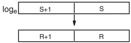
flowchart
graph TD
A["logₑ"] --> B["S+1"]
B --> C["S"]
D["R+1"] --> E["R"]
Source (32-bit floating-point data)
Result (32-bit floating-point data)
The source data must be positive; if it is negative, an error will occur and the instruction won't be executed.
If the absolute value of the result is greater than the maximum value that can be expressed as floating-point data, the Overflow Flag (SR 25404) will turn ON and the result will be output as ± .
Note The constant e is 2.718282.
The following diagram shows the relationship between the input data and result.
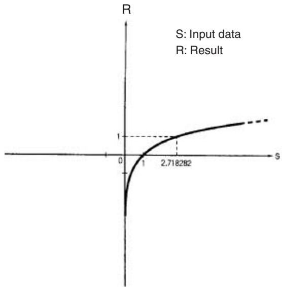
line
| S | R | | -------- | ------- | | 0 | 0 | | 2.718282 | 1 |Flags
ER: Indirectly addressed EM/DM word is non-existent.
(Content of *EM/*DM word is not BCD, or the EM/DM area boundary has been exceeded.)
ON if the source data is not recognized as floating-point data.
EQ: ON if both the exponent and mantissa of the result are 0.
OF: ON if the absolute value of the result is too large to be expressed as a 32-bit floating-point value. (The result will be output as ± .)
5-25 Logic Instructions
5-25-1 COMPLEMENT - COM(29)
Ladder Symbols
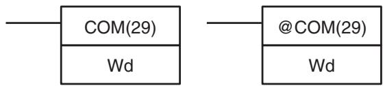
flowchart
graph LR
A["---"] --> B["COM(29)"]
B --> C["Wd"]
D["---"] --> E["@COM(29)"]
E --> F["Wd"]
Operand Data Areas
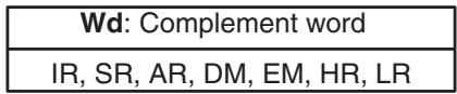
Limitations
DM 6144 to DM 6655 cannot be used for Wd.
Description
When the execution condition is OFF, COM(29) is not executed. When the execution condition is ON, COM(29) clears all ON bits and sets all OFF bits in Wd.
Precautions
The complement of Wd will be calculated every cycle if the undifferentiated form of COM(29) is used. Use the differentiated form (@COM(29)) or combine COM(29) with DIFU(13) or DIFD(14) to calculate the complement just once.
Example
Flags
ER: Indirectly addressed EM/DM word is non-existent. (Content of *EM/*DM word is not BCD, or the EM/DM area boundary has been exceeded.)
EQ: ON when the result is 0.
5-25-2 LOGICAL AND - ANDW(34)
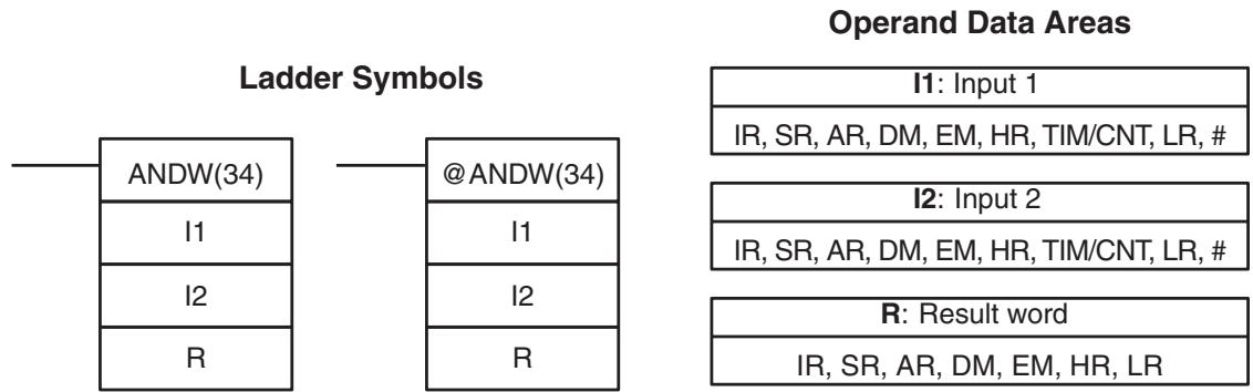
Limitations
DM 6144 to DM 6655 cannot be used for R.
Description
When the execution condition is OFF, ANDW(34) is not executed. When the execution condition is ON, ANDW(34) logically AND's the contents of I1 and I2 bit-by-bit and places the result in R.
Example

Flags
ER: Indirectly addressed EM/DM word is non-existent. (Content of *EM/*DM word is not BCD, or the EM/DM area boundary has been exceeded.) EQ: ON when the result is 0.
5-25-3 LOGICAL OR - ORW(35)
Ladder Symbols
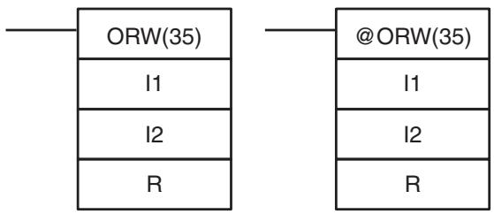
Operand Data Areas
| I1: Input 1 |
| IR, SR, AR, DM, EM, HR, TIM/CNT, LR, # |
| I2: Input 2 |
| IR, SR, AR, DM, EM, HR, TIM/CNT, LR, # |
| R: Result word |
| IR, SR, AR, DM, EM, HR, LR |
Limitations
DM 6144 to DM 6655 cannot be used for R.
Description
When the execution condition is OFF, ORW(35) is not executed. When the execution condition is ON, ORW(35) logically OR's the contents of I1 and I2 bit-by-bit and places the result in R.
Example
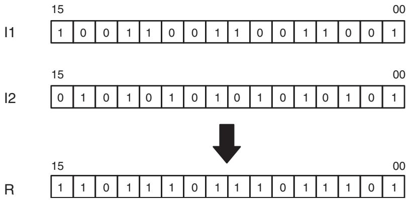
Flags
ER: Indirectly addressed EM/DM word is non-existent. (Content of *EM/*DM word is not BCD, or the EM/DM area boundary has been exceeded.)
EQ: ON when the result is 0.
5-25-4 EXCLUSIVE OR - XORW(36)
Ladder Symbols
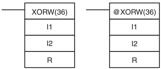
Operand Data Areas
| I1: Input 1 |
| IR, SR, AR, DM, EM, HR, TIM/CNT, LR, # |
| I2: Input 2 |
| IR, SR, AR, DM, EM, HR, TIM/CNT, LR, # |
| R: Result word |
| IR, SR, AR, DM, EM, HR, LR |
Limitations
DM 6144 to DM 6655 cannot be used for R.
Description
When the execution condition is OFF, XORW(36) is not executed. When the execution condition is ON, XORW(36) exclusively OR's the contents of I1 and I2 bit-by-bit and places the result in R.
Example

Flags
ER: Indirectly addressed EM/DM word is non-existent. (Content of *EM/*DM word is not BCD, or the EM/DM area boundary has been exceeded.)
EQ: ON when the result is 0.
5-25-5 EXCLUSIVE NOR – XNRW(37)
Ladder Symbols
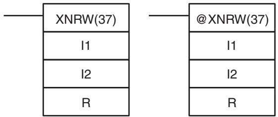
Operand Data Areas
| I1: Input 1 |
| IR, SR, AR, DM, EM, HR, TIM/CNT, LR, # |
| I2: Input 2 |
| IR, SR, AR, DM, EM, HR, TIM/CNT, LR, # |
| R: Result word |
| IR, SR, AR, DM, EM, HR, LR |
Limitations
DM 6144 to DM 6655 cannot be used for R.
Description
When the execution condition is OFF, XNRW(37) is not executed. When the execution condition is ON, XNRW(37) exclusively NOR's the contents of I1 and I2 bit-by-bit and places the result in R.
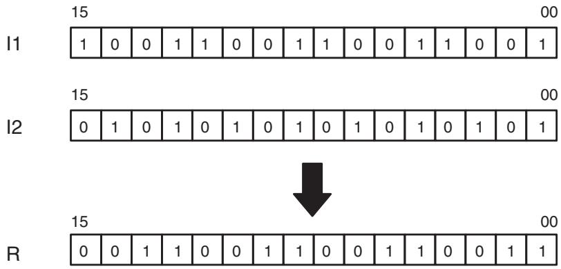
Flags
ER: Indirectly addressed EM/DM word is non-existent. (Content of *EM/*DM word is not BCD, or the EM/DM area boundary has been exceeded.) EQ: ON when the result is 0.
5-26 Increment/Decrement Instructions
5-26-1 BCD INCREMENT – INC(38)
Ladder Symbols
| INC(38)Wd | @INC(38)Wd |
Operand Data Areas
| Wd: Increment word (BCD) |
| IR, SR, AR, DM, EM, HR, LR |
Limitations DM 6144 to DM 6655 cannot be used for Wd.
Description When the execution condition is OFF, INC(38) is not executed. When the execution condition is ON, INC(38) increments Wd, without affecting Carry (CY).
Precautions The content of Wd will be incremented every cycle if the undifferentiated form of INC(38) is used. Use the differentiated form (@INC(38)) or combine INC(38) with DIFU(13) or DIFD(14) to increment Wd just once.
Flags ER: Wd is not BCD
Indirectly addressed EM/DM word is non-existent.
(Content of *EM/*DM word is not BCD, or the EM/DM area boundary has been exceeded.)
EQ: ON when the incremented result is 0.
5-26-2 BCD DECREMENT - DEC(39)
Ladder Symbols
| DEC(39)Wd | @DEC(39)Wd |
Operand Data Areas
| Wd: Decrement word (BCD) |
| IR, SR, AR, DM, EM, HR, LR |
Limitations DM 6144 to DM 6655 cannot be used for Wd.
Description When the execution condition is OFF, DEC(39) is not executed. When the execution condition is ON, DEC(39) decrements Wd, without affecting CY. DEC(39) works the same way as INC(38) except that it decrements the value instead of incrementing it.
Precautions The content of Wd will be decremented every cycle if the undifferentiated form of DEC(39) is used. Use the differentiated form (@DEC(39)) or combine DEC(39) with DIFU(13) or DIFD(14) to decrement Wd just once.
Flags ER: Wd is not BCD.
Indirectly addressed EM/DM word is non-existent.
(Content of *EM/*DM word is not BCD, or the EM/DM area boundary has been exceeded.)
EQ: ON when the decremented result is 0.
5-27 Subroutine Instructions
Subroutines break large control tasks into smaller ones and enable you to reuse a given set of instructions. When the main program calls a subroutine, control is transferred to the subroutine and the subroutine instructions are executed. The instructions within a subroutine are written in the same way as main program code. When all the subroutine instructions have been executed, control returns to the main program to the point just after the point from which the subroutine was entered (unless otherwise specified in the subroutine).
5-27-1 SUBROUTINE ENTER – SBS(91)
Ladder Symbol

Definer Data Areas
| N: Subroutine number |
| 000 to 255 |
Description
A subroutine can be executed by placing SBS(91) in the main program at the point where the subroutine is desired. The subroutine number used in SBS(91) indicates the desired subroutine. When SBS(91) is executed (i.e., when the execution condition for it is ON), the instructions between the SBN(92) with the same subroutine number and the first RET(93) after it are executed before execution returns to the instruction following the SBS(91) that made the call.
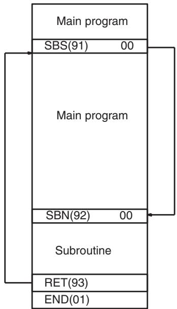
flowchart
graph TD
A["Main program"] --> B["SBS(91) 00"]
A --> C["Main program"]
C --> D["SBN(92) 00"]
C --> E["Subroutine"]
E --> F["RET(93)"]
E --> G["END(01)"]
SBS(91) may be used as many times as desired in the program, i.e., the same subroutine may be called from different places in the program).
SBS(91) may also be placed into a subroutine to shift program execution from one subroutine to another, i.e., subroutines may be nested. When the second subroutine has been completed (i.e., RET(93) has been reached), program execution returns to the original subroutine which is then completed before returning to the main program. Nesting is possible to up to sixteen levels. A subroutine cannot call itself (e.g., SBS(91) 000 cannot be programmed within the subroutine defined with SBN(92) 000). The following diagram illustrates two levels of nesting.
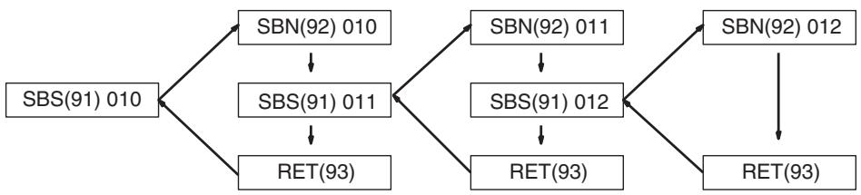
flowchart
graph TD
A["SBS(91) 010"] --> B["SBN(92) 010"]
A --> C["SBS(91) 011"]
A --> D["RET(93)"]
B --> E["SBN(92) 011"]
B --> F["SBS(91) 012"]
C --> G["RET(93)"]
E --> H["SBN(92) 012"]
F --> I["RET(93)"]
H --> J["RET(93)"]
The following diagram illustrates program execution flow for various execution conditions for two SBS(91).
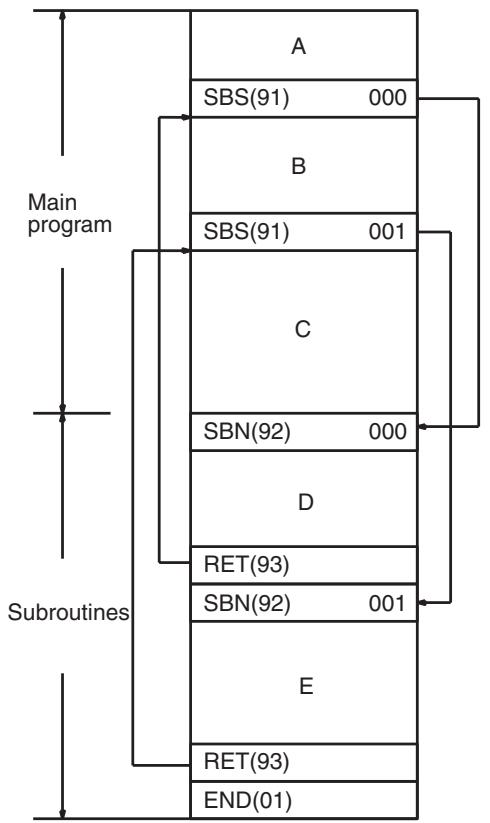
flowchart
graph TD
A["Main program"] --> B["SBS(91) 000"]
A --> C["SBS(91) 001"]
A --> D["SBN(92) 000"]
A --> E["D"]
A --> F["RET(93)"]
A --> G["SBN(92) 001"]
A --> H["E"]
A --> I["RET(93)"]
A --> J["END(01)"]
OFF execution conditions for subroutines 000 and 001

ON execution condition for subroutine 000 only
ON execution condition for subroutine 001 only
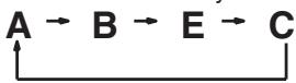
ON execution conditions for subroutines 000 and 001
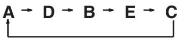
Flags
ER: A subroutine does not exist for the specified subroutine number.
A subroutine has called itself.
An active subroutine has been called.
Caution SBS(91) will not be executed and the subroutine will not be called when ER is ON.
5-27-2 SUBROUTINE DEFINE and RETURN – SBN(92)/RET(93)
| Ladder Symbols | Definer Data Areas | |
| SBN(92) N | N: Subroutine number000 to 255 | |
| RET(93) | ||
| Limitations | Each subroutine number can be used in SBN(92) only once. | |
| Description | SBN(92) is used to mark the beginning of a subroutine program; RET(93) is used to mark the end. Each subroutine is identified with a subroutine number N, that is programmed as a definer for SBN(92). This same subroutine number is used in any SBS(91) that calls the subroutine (see 5-27-1 SUBROUTINE ENTER – SBS(91). No subroutine number is required with RET(93).All subroutines must be programmed at the end of the main program. When one or more subroutines have been programmed, the main program will be executed up to the first SBN(92) before returning to address 00000 for the next cycle. Subroutines will not be executed unless called by SBS(91).END(01) must be placed at the end of the last subroutine program, i.e., after the last RET(93). It is not required at any other point in the program. | |
| Precautions | If SBN(92) is mistakenly placed in the main program, it will inhibit program execution past that point, i.e., program execution will return to the beginning when SBN(92) is encountered.If either DIFU(13) or DIFU(14) is placed within a subroutine, the operand bit will not be turned OFF until the next time the subroutine is executed, i.e., the operand bit may stay ON longer than one cycle. | |
| Flags | There are no flags directly affected by these instructions. | |
5-28 Special Instructions
5-28-1 TRACE MEMORY SAMPLING – TRSM(45)
Data tracing can be used to facilitate debugging programs. To set up and use data tracing it is necessary to have a host computer running SSS; no data tracing is possible from a Programming Console. Data tracing is described in detail in the SSS Operation Manual: C-series PCs. This section shows the ladder symbol for TRSM(45) and gives an example program.
Ladder Symbol
TRSM(45)
Description
TRSM(45) is used in the program to mark locations where specified data is to be stored in Trace Memory. Up to 12 bits and up to 3 words may be designated for tracing. (Refer to the CX-Programmer Operation Manual for details.) TRSM(45) is not controlled by an execution condition, but rather by two bits in the AR area: AR 2515 and AR 2514. AR 2515 is the Sampling Start bit. This bit is turned ON to start the sampling processes for tracing. The Sampling Start bit must not be turned ON from the program, i.e., it must be turned ON only from the peripheral device. AR 2514 is the Trace Start bit. When it is set,
the specified data is recorded in Trace Memory. The Trace Start bit can be set either from the program or from the Programming Device. A positive or negative delay can also be set to alter the actual point from which tracing will begin.
Data can be recorded in any of three ways. TRSM(45) can be placed at one or more locations in the program to indicate where the specified data is to be traced. If TRSM(45) is not used, the specified data will be traced when END(01) is executed. The third method involves setting a timer interval from the peripheral devices so that the specified data will be tracing at a regular interval independent of the cycle time. (Refer to the SSS Operation Manual: C-series PCs.)
TRSM(45) can be incorporated anywhere in a program, any number of times. The data in the trace memory can then be monitored via a Programming Console, host computer, etc.
AR Control Bits and Flags
The following control bits and flags are used during data tracing. The Tracing Flag will be ON during tracing operations. The Trace Completed Flag will turn ON when enough data has been traced to fill Trace Memory.
| Flag | Function |
| AR 2515 | Sampling Start Bit* |
| AR 2514 | Trace Start Bit |
| AR 2513 | Tracing Flag |
| AR 2512 | Trace Completed Flag |
Note *Do not change the status of AR 2515 from the program.
Precautions
If TRSM(45) occurs TRSM(45) will not be executed within a JMP(08) - JME(09) block when the jump condition is OFF.
Example
The following example shows the basic program and operation for data tracing. Force set the Sampling Start Bit (AR 2515) to begin sampling. The Sampling Start Bit must not be turned ON from the program. The data is read and stored into trace memory.
When IR 00000 is ON, the Trace Start Bit (AR 2514) is also turned ON, and the CPU Unit looks at the delay and marks the trace memory accordingly. This can mean that some of the samples already made will be recorded as the trace memory (negative delay), or that more samples will be made before they are recorded (positive delay).
The sampled data is written to trace memory, jumping to the beginning of the memory area once the end has been reached and continuing up to the start marker. This might mean that previously recorded data (i.e., data from this sample that falls before the start marker) is overwritten (this is especially true if the delay is positive). The negative delay cannot be such that the required data was executed before sampling was started.
flowchart
graph TD
A["00000"] --> B["AR 2514"]
B --> C["Starts data tracing."]
D["TRSM(45)"] --> E["Designates point for tracing."]
F["AR 2513 ON when tracing"] --> G["00200"]
H["AR 2512 ON when trace is complete"] --> I["00201"]
J["Indicates that tracing is in progress."] --> K["Indicates that tracing has been completed."]
| Address | Instruction | Operands |
| 00000 | LD | 0000 |
| 00001 | OUT | AR 2514 |
| 00002 | TRSM(45) | |
| 00003 | LD | AR 2513 |
| Address | Instruction | Operands |
| 00004 | OUT | 00200 |
| 00005 | LD | AR 2512 |
| 00006 | OUT | 00201 |
5-28-2 MESSAGE DISPLAY – MSG(46)
Ladder Symbols
flowchart
graph LR
A["MSG(46)"] --> B["FM"]
C["@MSG(46)"] --> D["FM"]
Operand Data Areas
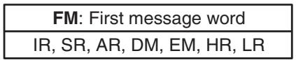
Limitations
Description
DM 6649 to DM 6655 cannot be used for FM.
When executed with an ON execution condition, MSG(46) reads eight words of extended ASCII code from FM to FM+7 and displays the message on the Programming Console. The displayed message can be up to 16 characters long, i.e., each ASCII character code requires eight bits (two digits). Refer to Appendix H for the ASCII codes. Japanese katakana characters are included in this code.
If not all eight words are required for the message, it can be stopped at any point by inputting “OD.” When OD is encountered in a message, no more words will be read and the words that normally would be used for the message can be used for other purposes.
Message Buffering and Priority
Up to three messages can be buffered in memory. Once stored in the buffer, they are displayed on a first in, first out basis. Since it is possible that more than three MSG(46)s may be executed within a single cycle, there is a priority scheme, based on the area where the messages are stored, for the selection of those messages to be buffered.
The priority of the data areas is as follows for message display:
$$ \mathrm{LR} > \mathrm{IR} > \mathrm{HR} > \mathrm{AR} > \text {TIM / CNT} > \mathrm{DM} $$
In handling messages from the same area, those with the lowest address values have higher priority.
In handling indirectly addressed messages (i.e. *DM), those with the lowest final DM addresses have higher priority.
Clearing Messages
To clear a message, execute FAL(06) 00 or clear it via a Programming Console or the SSS.
If the message data changes while the message is being displayed, the display will also change.
Flags
ER: Indirectly addressed EM/DM word is non-existent.
(Content of *EM/*DM word is not BCD, or the EM/DM area boundary has been exceeded.)
Example
The following example shows the display that would be produced for the instruction and data given when 00000 was ON. If 00001 goes ON, a message will be cleared.
flowchart
graph TD
A["00000"] --> B["MSG(46)"]
C["00001"] --> D["FAL(06) 00"]
B --> E["DM 0010"]
| Address | Instruction | Operands |
| 00000 | LD | 00000 |
| 00001 | MSG(46) | |
| DM 0010 | ||
| 00002 | LD | 00001 |
| 00003 | FAL(06) | 00 |
| DM contents | ASCII equivalent | |||||
| DM 0010 | 4 | 1 | 4 | 2 | A | B |
| DM 0011 | 4 | 3 | 4 | 4 | C | D |
| DM 0012 | 4 | 5 | 4 | 6 | E | F |
| DM 0013 | 4 | 7 | 4 | 8 | G | H |
| DM 0014 | 4 | 9 | 4 | A | I | J |
| DM 0015 | 4 | B | 4 | C | K | L |
| DM 0016 | 4 | D | 4 | E | M | N |
| DM 0017 | 4 | F | 5 | 0 | O | P |

5-28-3 I/O REFRESH – IORF(97)
Ladder Symbol
| IORF(97) |
| St |
| E |
Operand Data Areas
| St: Starting word |
| IR 000 to IR 115 |
| E: End word |
| IR 000 to IR 115 |
Limitations
St must be less than or equal to E.
Description
To refresh I/O words, specify the first (St) and last (E) I/O words to be refreshed. When the execution condition for IORF(97) is ON, all words between St and E will be refreshed. This will be in addition to the normal I/O refresh performed during the CPU Unit's cycle.
Note This instruction will have no effect on words that are not being used for I/O.
Flags
There are no flags affected by this instruction.
5-28-4 MACRO - MCRO(99)
Ladder Symbols
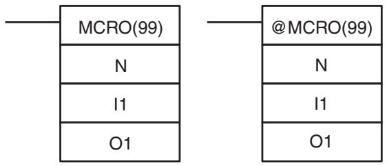
Operand Data Areas
| N: Subroutine number |
| 000 to 127 |
| I1: First input word |
| IR, SR, AR, DM, EM, HR, TIM/CNT, LR |
| O1: First output word |
| IR, SR, AR, DM, EM, HR, LR |
Limitations
Description
DM 6144 to DM 6655 cannot be used for O1.
The MACRO instruction allows a single subroutine to replace several subroutines that have identical structure but different operands. There are 4 input words, IR 096 to IR 099, and 4 output words, IR 196 to IR 199, allocated to MCRO(99). These 8 words are used in the subroutine and take their contents from I1 to I1+3 and O1 to O1+3 when the subroutine is executed.
When the execution condition is OFF, MCRO(99) is not executed. When the execution condition is ON, MCRO(99) copies the contents of I1 to I1+3 to IR 096 to IR 099, copies the contents of O1 to O1+3 to IR 196 to IR 199, and then calls and executes the subroutine specified in N. When the subroutine is completed, the contents of IR 196 through IR 199 is then transferred back to O1 to O1+3 before MCRO(99) is completed.
The macro function allows a single subroutine (programming pattern) to be used by simply changing the I/O word. A number of similar program sections can be managed with just one subroutine, thereby greatly reducing the number of steps in the program and making the program easier to understand.
Using Macros
To use a macro, call a subroutine by means of the MACRO instruction, MCRO(99), as shown below, instead of SBS(91) (SUBROUTINE ENTRY).
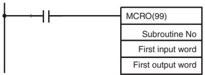
flowchart
graph TD
A["Start"] --> B["MCRO(99)"]
B --> C["Subroutine No"]
B --> D["First input word"]
B --> E["First output word"]
When MCRO(99) is executed, operation will proceed as follows:
1,2,3...
- The contents of the four consecutive words beginning with the first input word will be transferred to IR 096 through IR 099. The contents of the four consecutive words beginning with the first output word will be transferred to IR 196 through IR 199.
- The specified subroutine will be executed until RET(93) (Subroutine Return) is executed.
- The contents of IR 196 through IR 199 will be transferred to the four consecutive words beginning with the first output word.
- MCRO(99) will then be finished.
When MCRO(99) is executed, the same instruction pattern can be used as needed simply by changing the first input word or the first output word.
The following restrictions apply when the macro function is used.
- The only words that can be used for each execution of the macro are the four consecutive words beginning with the first input word number (for input) and the four consecutive words beginning with the first output word (for output).
- The specified inputs and outputs must correctly correspond to the words used in the subroutine.
- Even when the direct output method is used for outputs, subroutine results will be actually reflected in the specified output words only when the subroutine has been completed (step 3 above).
Note IR 096 to IR 099 and IR 196 to IR 199 can be used as work bits when MCRO(99) is not used.
The first input word and the first output word can be specified not only with I/O bits, but also with other bits (such as HR bits, work bits, etc.) or with DM words.
Subroutines called by MCRO(99) are defined by SBN(92) and RET(93), just as are ordinary subroutines.
Application Example
When a macro is used, the program can be simplified as shown below.
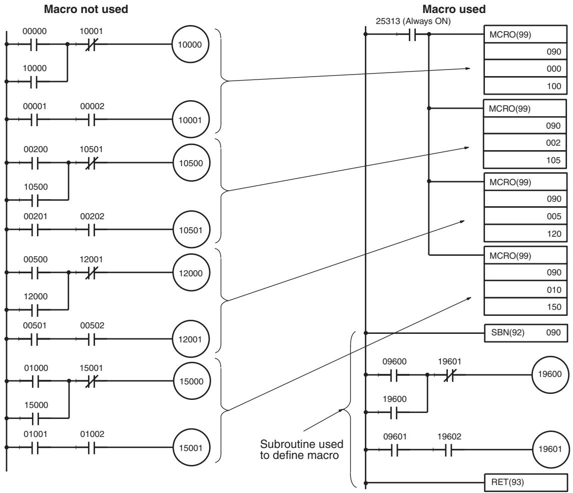
flowchart
graph TD
A["00000"] --> B["10001"]
C["10000"] --> D["10000"]
E["00001"] --> F["00002"]
G["00200"] --> H["10501"]
I["10500"] --> J["10500"]
K["00201"] --> L["00202"]
M["00500"] --> N["12001"]
O["12000"] --> P["12000"]
Q["00501"] --> R["00502"]
S["01000"] --> T["15001"]
U["15000"] --> V["15000"]
W["01001"] --> X["01002"]
Y["15001"] --> Z["Subroutine used to define macro"]
subgraph "Macro not used"
B --> D
D --> F
F --> H
H --> J
J --> N
N --> P
P --> R
R --> S
S --> U
U --> W
W --> X
X --> Y
end
subgraph "Macro used"
D --> Z
end
subgraph "Subroutine used to define macro"
Z --> AA["25313 (Always ON)"]
AA --> AB["MCRO(99)"]
AA --> AC["MCRO(99)"]
AA --> AD["MCRO(99)"]
AA --> AE["SBN(92)"]
AA --> AF["RET(93)"]
end
subgraph "Subroutine used to define macro"
AA --> AG["9600"]
AA --> AH["19601"]
AA --> AI["19600"]
AA --> AJ["9601"]
AA --> AK["19602"]
AA --> AL["19601"]
end
Flags
ER: A subroutine does not exist for the specified subroutine number. An operand has exceeded a data area boundary.
Indirectly addressed EM/DM word is non-existent.
(Content of *EM/*DM word is not BCD, or the EM/DM area boundary has been exceeded.)
A subroutine has called itself.
An active subroutine has been called.
5-28-5 BIT COUNTER - BCNT(67)
Ladder Symbols
Operand Data Areas
Limitations
N cannot be 0.
DM 6144 to DM 6655 cannot be used for R.
Description
When the execution condition is OFF, BCNT(67) is not executed. When the execution condition is ON, BCNT(67) counts the total number of bits that are ON in all words between SB and SB+(N-1) and places the result in R.
Flags
ER: N is not BCD, or N is 0; SB and SB+(N-1) are not in the same area.
The resulting count value exceeds 9999.
Indirectly addressed EM/DM word is non-existent.
(Content of *EM/*DM word is not BCD, or the EM/DM area boundary has been exceeded.)
EQ: ON when the result is 0.
5-28-6 FRAME CHECKSUM - FCS(--)
Ladder Symbols
Operand Data Areas
| C: Control data |
| IR, SR, AR, DM, EM, HR, LR, # |
R_1 : First word in range
IR, SR, AR, DM, EM, HR, TIM/CNT, LR
D: First destination word
IR, SR, AR, DM, EM, HR, LR
Limitations
The 3 rightmost digits of C must be BCD between 001 and 999.
DM 6143 to DM 6655 cannot be used for D.
Description
FCS(—) can be used to check for errors when transferring data through communications ports.
When the execution condition is OFF, FCS(—) is not executed. When the execution condition is ON, FCS(—) calculates the frame checksum of the specified range by exclusively ORing either the contents of words R_1 to R_1+N-1 or
the bytes in words R_1 to R_1+N-1 . The frame checksum value (hexadecimal) is then converted to ASCII and output to the destination words (D and D+1).
The function of bits in C are shown in the following diagram and explained in more detail below.
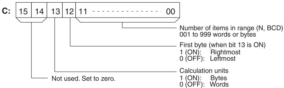
Number of Items in Range
The number of items within the range (N) is contained in the 3 rightmost digits of C, which must be BCD between 001 and 999.
Calculation Units
The frame checksum of words will be calculated if bit 13 is OFF and the frame checksum of bytes will be calculated if bit 13 is ON.
If bytes are specified, the range can begin with the leftmost or rightmost byte of R_1 . The leftmost byte of R_1 will not be included if bit 12 is ON.
| MSB | LSB | |
| R_1 | 1 | 2 |
| R_1+1 | 3 | 4 |
| R_1+2 | 5 | 6 |
| R_1+3 | 7 | 8 |
| | | | | | |
| | | | | | |
| | | | | | |
When bit 12 is OFF the bytes will be ORed in this order: 1, 2, 3, 4, ....
When bit 12 is ON the bytes will be ORed in this order: 2, 3, 4, 5, ....
Conversion to ASCII
The byte frame checksum calculation yields a 2-digit hexadecimal value which is converted to its 4-digit ASCII equivalent. The word frame checksum calculation yields a 4-digit hexadecimal value which is converted to its 8-digit ASCII equivalent, as shown below.
Byte frame checksum value
Word frame checksum value
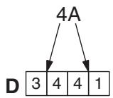
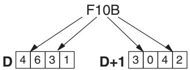
flowchart
graph TD
A["F10B"] --> B["D"]
A --> C["D+1"]
B --> D["4"]
B --> E["6"]
B --> F["3"]
B --> G["1"]
C --> H["3"]
C --> I["0"]
C --> J["4"]
C --> K["2"]
Flags
ER: Indirectly addressed EM/DM word is non-existent.
(Content of *EM/*DM word is not BCD, or the EM/DM area boundary has been exceeded.)
The number of items is not 001 to 999 BCD.
Example
When IR 00000 is ON in the following example, the frame checksum (0008) is calculated for the 8 words from DM 0000 to DM 0007 and the ASCII equivalent (30 30 30 38) is written to DM 0010 and DM 0011.
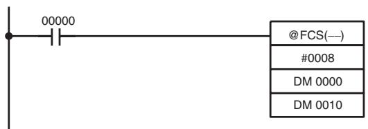
| Address | Instruction | Operands |
| 00000 | LD | 00000 |
| 00001 | @FCS(--) | |
| # 0008 | ||
| DM 0000 | ||
| DM 0010 |
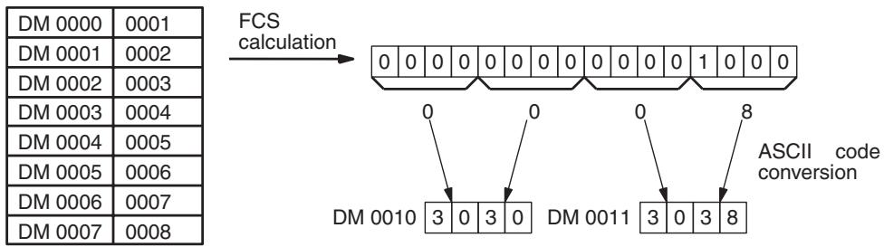
flowchart
graph TD
A["DM 0000 0001"] --> B["FCS calculation"]
C["DM 0001 0002"] --> B
D["DM 0002 0003"] --> B
E["DM 0003 0004"] --> B
F["DM 0004 0005"] --> B
G["DM 0005 0006"] --> B
H["DM 0006 0007"] --> B
I["DM 0007 0008"] --> B
B --> J["ASCII code conversion"]
J --> K["DM 0010 3 0 3 0 DM 0011 3 0 3 8"]
K --> L["0 0 0 0 0 0 0 0 0 0 1 0 0 0"]
L --> M["0 8"]
5-28-7 FAILURE POINT DETECTION - FPD(—)
Ladder Symbols
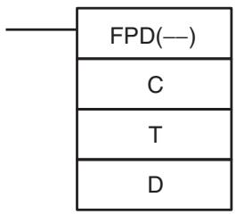
flowchart
graph TD
A["FPD(—)"] --> B["C"]
B --> C["T"]
C --> D["D"]
Operand Data Areas
| C: Control data |
| # |
| T: Monitoring time (BCD) |
| IR, SR, AR, DM, EM, HR, TIM/CNT. LR, # |
| D: First register word |
| IR, SR, AR, DM, EM, HR, LR |
Limitations
D and D+8 must be in the same data area when bit 15 of C is ON.
DM 6144 to DM 6655 cannot be used for T or D.
C must be input as a constant.
Description
FPD(—) can be used in the program as many times as desired, but each must use a different D. It is used to monitor the time between the execution of FPD(—) and the execution of a diagnostic output. If the time exceeds T, an FAL(06) non-fatal error will be generated with the FAL number specified in C.
The program sections marked by dashed lines in the following diagram can be written according to the needs of the particular program application. The processing programming section triggered by CY is optional and can be used any instructions but LD and LD NOT. The logic diagnostic instructions and execution condition can consist of any combination of NC or NO conditions desired.
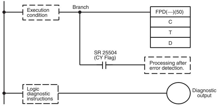
flowchart
graph TD
A["Execution condition"] --> B["Branch"]
B --> C["SR 25504 (CY Flag)"]
C --> D["Processing after error detection."]
D --> E["Diagnostic output"]
F["Logic diagnostic instructions"] --> E
G["FPD(—)(50)"] --> H["C"]
G --> I["T"]
G --> J["D"]
When the execution condition is OFF, FPD(—) is not executed. When the execution condition is ON, FPD(—) monitors the time until the logic diagnostics condition goes ON, turning ON the diagnostic output. If this time exceeds T, the following will occur:
1,2,3...
- An FAL(06) error is generated with the FAL number specified in the first two digits of C. If 00 is specified, however, an error will not be generated.
- The logic diagnostic instructions are searched for the first OFF input condition and this condition's bit address is output to the destination words beginning at D.
- The CY Flag (SR 25504) is turned ON. An error processing program section can be executed using the CY Flag if desired.
- If bit 15 of C is ON, a preset message with up to 8 ASCII characters will be displayed on the Peripheral Device along with the bit address mentioned in step 2.
Control Data
The function of the control data bits in C are shown in the following diagram.
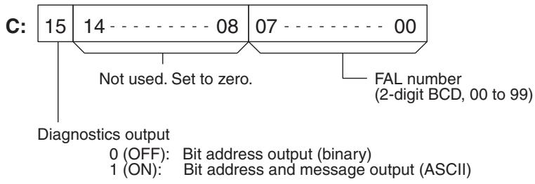
Logic Diagnostic Instructions
If the time until the logic diagnostics condition goes ON exceeds T, the logic diagnostic instructions are searched for the OFF input condition. If more than one input condition is OFF, the input condition on the highest instruction line and nearest the left bus bar is selected.
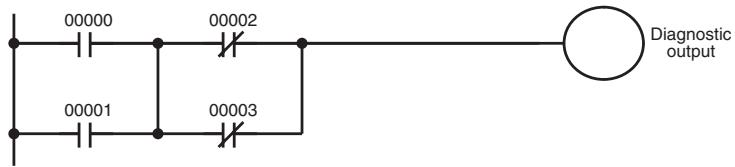
When IR 00000 to IR 00003 are ON, the normally closed condition IR 00002 would be found as the cause of the diagnostic output not turning ON.
Diagnostics Output
There are two ways to output the bit address of the OFF condition detected in the logic diagnostics condition.
1,2,3... 1. Bit address output (used when bit 15 of C is OFF).
Bit 15 of D indicates whether or not bit address information is stored in D+1. If there is, bit 14 of D indicates whether the input condition is normally open or closed.
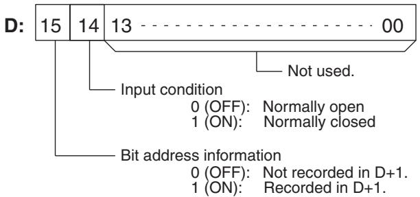
D+1 contains the bit address code of the input condition, as shown below. The word addresses, bit numbers, and TIM/CNT numbers are in binary.
| Data Area | D+1 bit status | |||||||||||||||
| 15 | 14 | 13 | 12 | 11 | 10 | 09 | 08 | 07 | 06 | 05 | 04 | 03 | 02 | 01 | 00 | |
| IR, SR | 1 | 0 | 0 | 0 | Word address | Bit number | ||||||||||
| HR | 1 | 0 | 0 | 1 | 1 | Word address | Bit number | |||||||||
| LR | 1 | 0 | 0 | 1 | 0 | 0 | Word address | Bit number | ||||||||
| TIM/CNT* | 1 | 0 | 0 | 1 | 0 | 1 | * | Timer or counter number | ||||||||
Note a) *For the TIM/CNT area, bit 09 of D+1 indicates whether the number is a timer or counter. A 0 indicates a timer, and a 1 indicates a counter.
b) The status of the leftmost bit of the bit number (bit 03) is reversed.
Example: If D + 1 contains 1000 0110 0100 1000, IR 10000 would be indicated as follows:
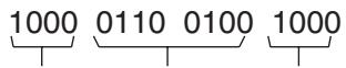
IR
\$64 = 100
Bit 00 (inverting status of bit 03)
- Bit address and message output (selected when bit 15 of C is ON).
Bit 15 of D indicates whether or not there is bit address information stored in D+1 to D+3. If there is, bit 14 of D indicates whether the input condition is normally open or closed. Refer to the following table.
Words D+5 to D+8 contain information in ASCII that are displayed on a Peripheral Device along with the bit address when FPD(—) is executed. Words D+5 to D+8 contain the message preset by the user as shown in the following table.
| Word | Bits 15 to 08 | Bits 07 to 00 |
| D+1 | 20 = space | First ASCII character |
| D+2 | Second ASCII character | Third ASCII character |
| D+3 | Fourth ASCII character | Fifth ASCII character |
| D+4 | 2D = “-” | “0”=normally open, “1”=normally closed |
| D+5 | First ASCII character | Second ASCII character |
| D+6 | Third ASCII character | Fourth ASCII character |
| D+7 | Fifth ASCII character | Sixth ASCII character |
| D+8 | Seventh ASCII character | Eighth ASCII character |
Note If 8 characters are not needed in the message, input "0D" after the last character.
Determining Monitoring Time
The procedure below can be used to automatically set the monitoring time, T, under actual operating conditions when specifying a word operand for T. This operation cannot be used if a constant is set for T.
1,2,3...
- Switch the CQM1H to MONITOR Mode operation.
- Connect a Peripheral Device, such as a Programming Console.
- Use the Peripheral Device to turn ON control bit AR 2508.
- Execute the program with AR 2508 turned ON. If the monitoring time currently in T is exceeded, 1.5 times the actual monitoring time will be stored in T. FAL(06) errors will not occur while AR 2508 is ON.
- Turn OFF AR 2508 when an acceptable value has been stored in T.
Example
In the following example, the FPD(—) is set to display the bit address and message (“ABC”) when a monitoring time of 123.4 s is exceeded.
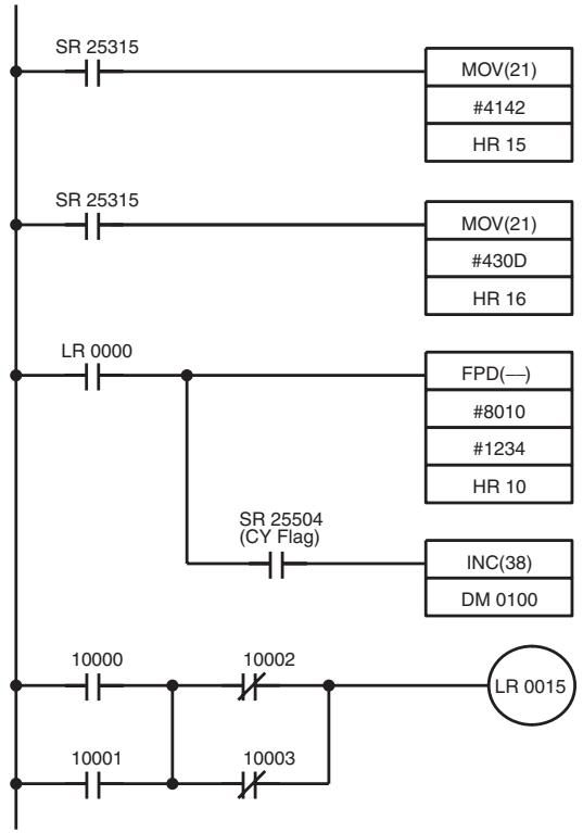
flowchart
graph TD
A["SR 25315"] --> B["MOV(21)"]
A --> C["#4142"]
A --> D["HR 15"]
E["SR 25315"] --> F["MOV(21)"]
E --> G["#430D"]
E --> H["HR 16"]
I["LR 0000"] --> J["FPD(—)"]
I --> K["#8010"]
I --> L["#1234"]
I --> M["HR 10"]
N["SR 25504 (CY Flag)"] --> O["INC(38)"]
N --> P["DM 0100"]
Q["10000"] --> R["10002"]
S["10001"] --> T["10003"]
U["LR 0015"] --> V["Ground"]
| Address | Instruction | Operands |
| 00000 | LD | 25315 |
| 00001 | MOV(21) | |
| # 4142 | ||
| HR 15 | ||
| 00002 | LD | 25315 |
| 00003 | MOV(21) | |
| # 430D | ||
| HR 16 | ||
| 00004 | LD | LR 0000 |
| 00005 | FPD(—) | |
| # 0010 | ||
| # 1234 | ||
| HR 10 | ||
| 00006 | AND | 25504 |
| 00007 | INC(38) | |
| DM 0100 | ||
| 00008 | LD | 10000 |
| 00009 | OR | 10001 |
| 00010 | LD NOT | 10002 |
| 00011 | OR NOT | 10003 |
| 00012 | AND LD | |
| 00013 | OUT | LR 0015 |
FPD(—) is executed and begins monitoring when LR 0000 goes ON. If LR 0015 does not turn ON within 123.4 s and IR 10000 through IR 10003 are all ON, IR 10002 will be selected as the cause of the error, an FAL(06) error will be generated with an FAL number of 10, and the bit address and preset message (“10002–1ABC”) will be displayed on the Peripheral Device.
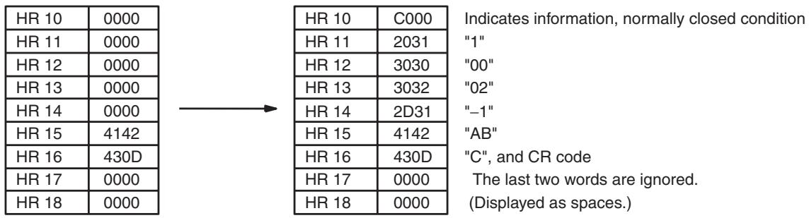
Flags
ER: T is not BCD.
C is not a constant or is not BCD 00 to 99.
Indirectly addressed EM/DM word is non-existent.
(Content of *EM/*DM word is not BCD, or the EM/DM area boundary has been exceeded.)
CY: ON when the time between the execution of FPD(—) and the execution of a diagnostic output exceeds T.
5-28-8 INTERRUPT CONTROL - INT(89)
Operand Data Areas
| Ladder Symbols | |
| INT(89) | @INT(89) |
| CC | CC |
| 000 | 000 |
| D | D |
Limitations
DM 6644 to DM 6655 cannot be used for D when CC=002.
Description
When the execution condition is OFF, INT(89) is not executed. When the execution condition is ON, INT(89) is used to control interrupts and performs one of the six functions shown in the following table depending on the value of CC.
Note Refer to 1-4 Interrupt Functions for more details.
| INT(89) function | CC |
| Mask/unmask input interrupts | 000 |
| Clear input interrupts | 001 |
| Read current mask status | 002 |
| Renew counter SV | 003 |
| Mask all interrupts | 100 |
| Unmask all interrupts | 200 |
Mask/Unmask I/O Interrupts (CC=000)
These six functions are described in more detail below. Refer to page 44 for more information on these functions.
This function is used to mask and unmask I/O interrupt inputs 00000 to 00003. Masked inputs are recorded, but ignored. When an input is masked, the interrupt program for it will be run as soon as the bit is unmasked (unless it is cleared beforehand by executing INT(89) with CC=001).
Set the corresponding bit in D to 0 or 1 to unmask or mask an I/O interrupt input. Bits 00 to 03 correspond to 00000 to 00003. Bits 04 to 15 should be set to 0.
Word D bits:
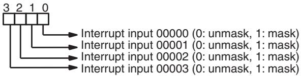
flowchart
graph TD
A["3"] --> B["Interrupt input 00000 (0: unmask, 1: mask)"]
C["2"] --> D["Interrupt input 00001 (0: unmask, 1: mask)"]
E["1"] --> F["Interrupt input 00002 (0: unmask, 1: mask)"]
G["0"] --> H["Interrupt input 00003 (0: unmask, 1: mask)"]
Clear I/O Interrupts (CC=001)
This function is used to clear I/O interrupt inputs 00000 to 00003. Since interrupt inputs are recorded, masked interrupts will be serviced after the mask is removed unless they are cleared first.
Set the corresponding bit in D to 1 to clear an I/O interrupt input. Bits 00 to 03 correspond to 00000 to 00003. Bits 04 to 15 should be set to 0.
Word D bits:
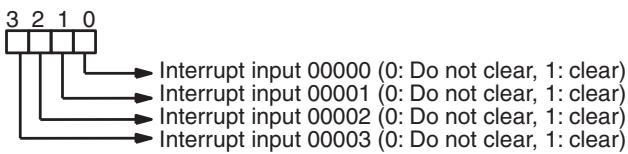
flowchart
graph TD
A["3"] --> B["Interrupt input 00000 (0: Do not clear, 1: clear)"]
A --> C["Interrupt input 00001 (0: Do not clear, 1: clear)"]
A --> D["Interrupt input 00002 (0: Do not clear, 1: clear)"]
A --> E["Interrupt input 00003 (0: Do not clear, 1: clear)"]
Read Current Mask Status (CC=002)
This function is used to write the current mask status for I/O interrupt inputs 00000 to 00003 to word D. The corresponding bit will be ON if the input is masked. (Bits 00 to 03 correspond to 00000 to 00003.)
Word D bits:
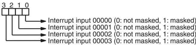
flowchart
graph TD
A["3"] --> B["Interrupt input 00000 (0: not masked, 1: masked)"]
A --> C["Interrupt input 00001 (0: not masked, 1: masked)"]
A --> D["Interrupt input 00002 (0: not masked, 1: masked)"]
A --> E["Interrupt input 00003 (0: not masked, 1: masked)"]
Renew Counter SV (CC=003)
This function is used to renew the counter SV for I/O interrupt inputs 00000 to 00003 to word D. Set the corresponding bit in D to 1 in order to renew the input's counter SV. (Bits 00 to 03 correspond to 00000 to 00003.)
Word D bits:
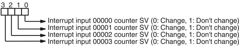
flowchart
graph TD
A["3"] --> B["Interrupt input 00000 counter SV (0: Change, 1: Don't change)"]
C["2"] --> D["Interrupt input 00001 counter SV (0: Change, 1: Don't change)"]
E["1"] --> F["Interrupt input 00002 counter SV (0: Change, 1: Don't change)"]
G["0"] --> H["Interrupt input 00003 counter SV (0: Change, 1: Don't change)"]
Mask/Unmasking All Interrupts (CC=100/200)
This function is used to mask or unmask all interrupt processing. Masked inputs are recorded, but ignored. Refer to page 30 for details.
The control data, D, is not used for this function. Set D to #0000.
Flags
ER: A counter's SV is incorrect. (CC=003 only)
Indirectly addressed EM/DM word is non-existent.
(Content of *EM/*DM word is not BCD, or the EM/DM area boundary has been exceeded.)
CC=100 or 200 while an interrupt program was being executed.
CC=100 when all inputs were already masked.
CC=200 when all inputs were already unmasked.
CC and/or D are not within specified values.
5-28-9 SET PULSES – PULS(65)
Ladder Symbols
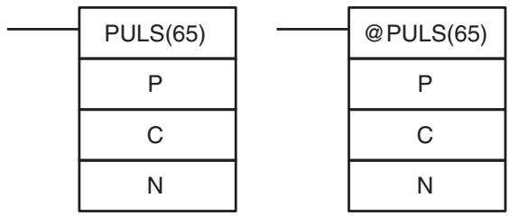
Operand Data Areas
| P: Port specifier |
| 000, 001 |
| C: Control data |
| 000 to 005 |
| N: Number of pulses |
| IR, SR, AR, DM, EM, HR, LR |
Limitations
N and N+1 must be in the same data area.
DM 6143 to DM 6655 cannot be used for N.
Description
PULS(65) can be used with the functions listed in the following table.
| Unit/Board | Function |
| Transistor Output Unit | Pulse outputs |
| Pulse I/O Board | Pulse outputs 1 and 2 |
PULS(65) is used to set parameters for pulse outputs that are started later in the program using SPED(64) or ACC(—). The parameters that can be set are the number of pulses that will be output in independent mode, the direction of pulse outputs from ports 1 and 2, and the deceleration point for pulse outputs controlled by ACC(—) mode 0.
Since PULS(65) has a relatively long execution time, the cycle time can be reduced by executing the differentiated version (@PULS(65)) of this instruction only when it is needed.
Note Refer to 1-5 Pulse Output Function for more details.
Port Specifier (P)
The port specifier indicates the pulse output location. The parameters set in C and N will apply to the next SPED(64) or ACC(—) instruction in which the same port output location is specified.
| Pulse output location | P |
| Output bits 00 to 15 (See note.) | 000 |
| Port 1 | 001 |
| Port 2 | 002 |
Note The bit between 00 and 15 that is output as the contact pulse is specified by the P operand in SPED(64),
Control Data (C)
The control data determines the direction of the pulse output to ports 1 and 2 and indicates whether the number of pulses and/or the deceleration point are specified in N to N+3. This operand should be set to 000 when an output bit is specified in P (P=□□0).
| C | Direction | Number of pulses | Deceleration point |
| 000 | CW | Set in N and N+1 | Not set. |
| 001 | CCW | Set in N and N+1 | Not set. |
| 002 | CW | Set in N and N+1 | Set in N+2 and N+3 |
| 003 | CCW | Set in N and N+1 | Set in N+2 and N+3 |
| 004 | CW | Not set. | Not set. |
| 005 | CCW | Not set. | Not set. |
The direction setting is valid until program execution is stopped or PULS(65) is executed again.
Number of Pulses (C=000 or C=001)
When C=000 or 001, N+1, N contains the 8-digit number of pulses setting for independent mode pulse outputs. N+1, N can be from 0000 0001 to 1677 7215. The pulse output started by SPED(64) or ACC(—) will stop automatically when this number of pulses has been output.
Leftmost 4 digits
Rightmost 4 digits
Possible range
Number of pulses:
N+1
N
0000 0001 to 1677 7215
Number of Pulses and Deceleration Point (C=002 or C=003)
When C=002 or 003, N+1, N contains the 8-digit number of pulses setting for independent mode pulse outputs. N+1, N can be from 0000 0001 to 1677 7215. The pulse output started by ACC(—) will stop automatically when this number of pulses has been output.
Leftmost 4 digits
Rightmost 4 digits
Possible range
Number of pulses:
N+1
N
0000 0001 to 1677 7215
N+3, N+2 contains the 8-digit number of pulses setting for the deceleration point used in ACC(—) mode 0. N+3, N+2 can be from 0000 0001 to 1677 7215. The pulse output started by ACC(—) will begin deceleration when this number of pulses have been output.
Leftmost 4 digits
Rightmost 4 digits
Possible range
Deceleration point:
N+3
N+2
0000 0001 to 1677 7215
Change Output Destination (C=004 or C=005)
When C=004 or 005, neither the number of pulses nor the deceleration point are set. Set N=000 when C=004 or 005. Use these settings to change the output destination for continuous mode pulse outputs from port 1 or port 2.
Frequency Changes
The number of pulses set to be output will be used even if SPED(64) is used to change the pulse frequency during operation. (The number of pulses cannot be changed during operation.)
For example, if the number of pulses setting is 2,100 and the frequency is changed from 1 KHz to 100 Hz, pulse output will stop in:
12 s if the pulse frequency is changed after 1 s at 1 KHz.
3 s if the pulse frequency is changed after 2 s at 1 KHz.
Flags
ER: Indirectly addressed EM/DM word is non-existent.
(Content of *EM/*DM word is not BCD, or the EM/DM area boundary has been exceeded.)
A data area boundary is exceeded.
There is an error in the instruction settings.
PULS(65) is executed in an interrupt subroutine while a pulse I/O or high-speed counter instruction is being executed in the main program.
5-28-10 SPEED OUTPUT- SPED(64)
Ladder Symbols
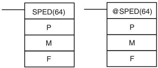
flowchart
graph TD
A["SPED(64)"] --> B["P"]
A --> C["M"]
A --> D["F"]
E["@SPED(64)"] --> F["P"]
E --> G["M"]
E --> H["F"]
Operand Data Areas
| P: Port specifier |
| 001, 002, or 010 to 150 |
| M: Output mode |
| 000 or 001 |
| F: Pulse frequency |
| IR, SR, AR, DM, EM, HR, LR, # |
Limitations
F must be BCD, #0000 to #5000 when a port is specified, #0000 or #0002 to #0100 when an output bit is specified.
DM 6144 to DM 6655 cannot be used for F.
Description
SPED(64) can be used with the functions listed in the following table.
| Unit/Board | Function |
| Transistor Output Unit | Pulse outputs |
| Pulse I/O Board | Pulse outputs 1 and 2 |
SPED(64) is used to set, change, or stop pulse output from the specified port or output bit. When the execution condition is OFF, SPED(64) is not executed. When the execution condition is ON, SPED(64) sets the pulse frequency F for the port or output bit specified by P. M determines the output mode.
Since SPED(64) has a relatively long execution time, the cycle time can be reduced by executing the differentiated version (@SPED(64)) of this instruction only when it is needed.
Note Refer to 1-5 Pulse Output Function for more details.
Port Specifier (P)
The port specifier specifies the port or output bit where the pulses will be output.
| P | Pulse output location |
| 001 | Port 1 |
| 002 | Port 2 |
| 000 to 150 | Output bits IR 10000 to IR 10015.The first two digits of P specify which bit of IR 100 is the output bit and the third digit of P is always set to 0. For example, P=000 specifies IR 10000, P=010 specifies IR 10001, ... and P=150 specifies bit IR 10015. |
Output Mode (M)
The value of M determines the output mode.
| M | Output mode |
| 000 | Independent mode, frequency set in units of 10 Hz |
| 001 | Continuous mode, frequency set in units of 10 Hz |
| 002 | Independent mode, frequency set in units of 1 Hz (See note.) |
| 003 | Continuous mode, frequency set in units of 1 Hz (See note.) |
Note Settings of 002 and 003 can be specified only for ports 1 and 2 of a Pulse I/O Board (P=001 or P=002).
In independent mode, the pulse output will continue until one of the following occurs:
1,2,3... 1. The number of pulses specified by the PULS(65) instruction is reached. (Execute PULS(65) before SPED(64) when specifying independent mode.)
- The INI(61) instruction is executed with C=003.
- SPED(64) is executed again with the output frequency, F, set to 000.
When outputting pulses in independent mode, specify the number of pulses beforehand by executing PULS(65). When outputting from port 1 or 2, specify the direction (CW or CCW) as well.
In independent mode, the number of pulses that have been output to ports 1 and 2 are contained in IR 236 and 237 (port 1) and IR 238 and IR 239 (port 2).
Leftmost 4 digits Rightmost 4 digits
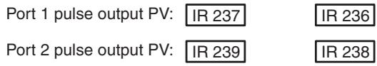
Although the number of pulses can be monitored in independent mode, the number of pulses cannot be monitored while pulses are being output in continuous mode.
In continuous mode, pulses will be output until the INI(61) instruction is executed with C=003 or SPED(64) is executed again with F=0000. If the direction (CW or CCW) is not specified when outputting from port 1 or 2, the pulses will be CW.
Pulse Frequency (F)
The value of F sets the pulse frequency, as shown below. Setting F to 0000 will stop the pulse output at the specified location.
| Output | Units | Possible values of F |
| Output bits | 10 Hz | 0000 (Stops output.) or 0002 to 0100 (20 Hz to 1 kHz) |
| Port 1 or 2 | 10 Hz | 0000 (Stops output.) or 0001 to 5000 (10 Hz to 50 kHz) |
| 1 Hz | 0000 (Stops output.) or 0010 to 9999 (10 Hz to 9,999 Hz) |
Precautions Regarding Pulse Output
The pulse frequency output from the CQM1H-PLB21 Pulse I/O Board is generated by dividing the 500-kHz basic clock pulse by an integer value, which results in a difference between the set frequency and actual frequency. Refer to the following equation for calculating an actual frequency.
Set Frequency: Output frequency set in the instruction by the user
Dividing Unit: An integer set in the dividing circuit to generate an output pulse of the set frequency
Actual Frequency: Output pulse frequency actually output from the dividing circuit
flowchart
graph LR
A["Pulse-generating clock"] --> B["500 kHz"]
B --> C["Dividing circuit"]
C --> D["Output pulse (actual frequency)"]
style C fill:#f9f,stroke:#333
note right of C: The dividing unit is set based on the frequency set by the user.
Equation:
Actual frequency (KHz) = 500 (KHz)/INT (500 (kHz)/Set frequency (kHz))
INT: Function for obtaining an integer value
INT (500/Set frequency): Dividing unit
The difference between the set frequency and actual frequency becomes larger as the frequency becomes higher.
Example:
| Set frequency (kHz) | Actual frequency (kHz) |
| 45.46 to 50.00 | 50.00 |
| 41.67 to 45.45 | 45.45 |
| 38.47 to 41.66 | 41.67 |
| : | : |
| 31.26 to 33.33 | 33.33 |
| 29.42 to 31.25 | 31.25 |
| 27.78 to 29.41 | 29.41 |
| : | : |
| 20.01 to 20.83 | 20.83 |
| 19.24 to 20.00 | 20.00 |
| 18.52 to 19.23 | 19.23 |
| : | : |
| 10.01 to 10.20 | 10.20 |
| 9.81 to 10.00 | 10.00 |
| 9.62 to 9.80 | 9.80 |
| : | : |
| 5.01 to 5.05 | 5.05 |
| 4.96 to 5.00 | 5.00 |
| 4.90 to 4.95 | 4.95 |
| : | : |
| 3.02 to 3.03 | 3.03 |
| 3.00 to 3.01 | 3.01 |
| 2.98 to 2.99 | 2.99 |
| : | : |
Precautions
The pulse output cannot be used when interval timer 0 is operating.
When a pulse output with a frequency of 500 Hz or higher is output from an output bit, set interrupt processing for the TIMH(15) TIM/CNT numbers 000 to 003 by setting #0104 in DM 6629 of the PC Setup.
Only one output bit at a time can have a pulse output.
Note Pulse output can be stopped only when pulses are not currently being output. The Pulse Output Flag (AR 0515 or AR 0615) can be used to check pulse output status.
Flags
ER: SPED(64) is executed while interval timer 0 is operating.
Indirectly addressed EM/DM word is non-existent.
(Content of *EM/*DM word is not BCD, or the EM/DM area boundary has been exceeded.)
There is an error in the instruction settings.
SPED(64) is executed in an interrupt subroutine while a pulse I/O or high-speed counter instruction is being executed in the main program.
5-28-11 PULSE OUTPUT - PLS2(—)
Ladder Symbols
Operand Data Areas
| P: Communications port |
| 001 or 002 |
| D: Direction specifier |
| 000 or 001 |
| C: First control word |
| IR, SR, AR, DM, EM, HR, LR |
Limitations
PLS2(—) cannot be used if the PC Setup (DM 6611) is set to high-speed counter mode.
P must be 001 or 002 and D must be 000 or 001.
C to C+3 must be in the same data area.
Description
PLS2(—) can be used with the functions listed in the following table.
| Unit/Board | Function |
| Pulse I/O Board | Pulse outputs 1 and 2(The mode for ports 1 and 2 must be set to the simple positioning mode in DM 6611 of the PC Setup. PLS2(—) cannot be used if the mode is set to high-speed counter mode.) |
PLS2(—) is used to output a specified number of CW or CCW pulses from port 1 or 2. The pulse output accelerates to the target frequency at a specified rate and decelerates at the same rate. (Pulse output stops at 100 Hz.)
line
| Time | Target frequency | |------|------------------| | T₁ | 0 | | T₂ | 100 Hz | | T₁ | 0 |The following equations show how to calculate the approximate acceleration/ deceleration time T_1 and running time T_2 . Both times are in seconds.
$$ T _ {1} \cong 0. 0 0 0 4 \times \frac {\text { Target frequency }}{\text { Acceleration / deceleration rate }} $$
$$ T _ {2} \cong \frac {\text { Number of pulses } - (T _ {1} \times \text { Target frequency })}{\text { Target frequency }} $$
Note
- Although T_1 and T_2 will vary slightly depending on the operating conditions, the number of pulses output will be accurate.
- PLS2(—) will not operate if pulses are already being output from the specified port. Check the pulse output flags (AR 0515 for port 1 and AR 0615 for port 2) before executing PLS2(—).
- Refer to 1-5 Pulse Output Function for more details.
Operand Settings
P specifies the port where the pulses will be output. Pulses are output from port 1 when P=001, and pulses are output from port 2 when P=002.
D specifies whether the output signal is clockwise (CW) or counter-clockwise (CCW). The output is CW when D=000 and CCW when D=001.
The content of C determines the acceleration/deceleration rate. During acceleration or deceleration, the output frequency is increased or decreased by the amount set in C every 4.08 ms. C must be BCD from 0001 to 0200 (10 Hz to 2 kHz).
The content of C+1 specifies the target frequency. C+1 must be BCD from 0010 to 5000 (100 Hz to 50 kHz).
The 8-digit content of C+3,C+2 determines the number of pulses that will be output. C+3, C+2 must be BCD between 0000 0001 and 1677 7215.
Flags
ER: Indirectly addressed EM/DM word is non-existent.
(Content of *EM/*DM word is not BCD, or the EM/DM area boundary has been exceeded.)
There is an error in the operand settings.
PLS2(—) is executed without a Pulse I/O Board installed.
The PC Setup is not set for pulse output.
The target frequency, acceleration/deceleration rate, and number of pulses are incorrect. (Number of pulses < T_1 × Target frequency )
PLS2(—) is executed in an interrupt subroutine while a pulse I/O or high-speed counter instruction is being executed in the main program.
AR 0515: Port 1 output flag. ON when pulses are being output from port 1.
AR 0615: Port 2 output flag. ON when pulses are being output from port 2.
Caution
With PLS2(—), conditions such as acceleration/deceleration speed and the target speed can cause low-speed pulse output (100 Hz) to continue for an extended period of time when stopping. Even when this happens, the correct number of pulses will be output.
Correct the system by adjusting the acceleration/deceleration speed and/or the target speed, or by using the ACC(—) instruction (mode 0) to increase the speed (deceleration target frequency) when stopping.
5-28-12 ACCELERATION CONTROL - ACC(—)
Ladder Symbols
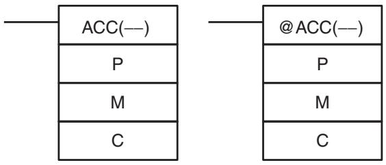
flowchart
graph TD
A["ACC(---)"] --> B["P"]
A --> C["M"]
A --> D["C"]
E["@ACC(---)"] --> F["P"]
E --> G["M"]
E --> H["C"]
Operand Data Areas
| P: Communications port |
| 001 or 002 |
| M: Mode specifier |
| 000 to 003 |
| C: First control word |
| IR, SR, AR, DM, EM, HR, LR |
Limitations
Mode 0 of ACC(—) cannot be used if the PC Setup (DM 6611) is set to high-speed counter mode.
P must be 001 or 002 and M must be 000 to 003.
C to C+3 must be in the same data area.
Description
ACC(—) can be used with the functions listed in the following table.
| Unit/Board | Function |
| Pulse I/O Board | Pulse outputs 1 and 2(In order to use ACC(—) mode 0, ports 1 and 2 must be set simple positioning mode in DM 6611 of the PC Setup. ACC(—) cannot be used if the mode is set to high-speed counter mode.) |
ACC(—) is used together with PULS(65) to control the acceleration and/or deceleration of pulses output from port 1 or 2. The 4 available modes are described briefly below.
The function of the control words varies in the 4 modes, but P always specifies the port where the pulses will be output and M always specifies the mode. Set P=001 or 002 to indicate port 1 or 2. Set M=000 to 003 to indicate modes 0 to 3.
Note Refer to 1-5 Pulse Output Function for more details.
Mode 0 (M=000)
Mode 0 is used to output a specified number of CW or CCW pulses from port 1 or 2. The acceleration rate, frequency after acceleration, deceleration point, deceleration rate, and frequency after deceleration can all be controlled.
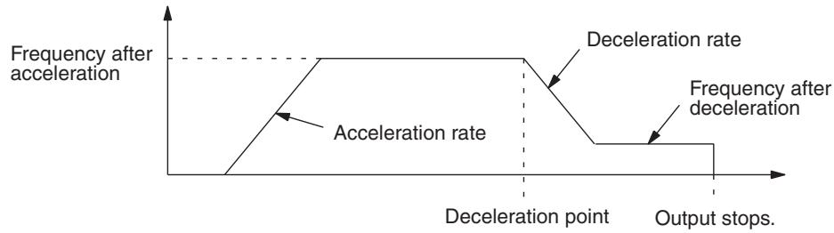
line
| Deceleration point | Frequency after deceleration | | ------------------ | ---------------------------- | | 0 | 0 | | Peak | Deceleration rate | | Output stops | Frequency after deceleration |PULS(65) Operand Settings
PULS(65) must be executed before ACC(—) in order to specify direction, the total number of pulses to be output, and the deceleration point. The function of PULS(65) operands are described below. Refer to 5-28-9 SET PULSES – PULS(65) for more details.
1,2,3... 1. The first operand of PULS(65) specifies the output port. Pulses are output from port 1 when P=001, and from port 2 when P=002.
- The second operand specifies the direction. The output is clockwise (CW) when C=002 and counter-clockwise (CCW) when C=003.
- The third operand specifies the first of 4 control words.
a) The 8-digit content of N+1, N (0000 0001 to 1677 7215) determines the total number of pulses that will be output.
b) The 8-digit content of N+3, N+2 (0000 0001 to 1677 7215) determines the deceleration point.
ACC(—) Control Words
The 4 control words indicate the acceleration rate, frequency after acceleration, deceleration rate, and frequency after deceleration.
1,2,3...
- The content of C determines the acceleration rate. During acceleration, the output frequency is increased by the amount set in C every 4.08 ms. C must be BCD from 0001 to 0200 (10 Hz to 2 kHz).
- The content of C+1 specifies the frequency after acceleration. C+1 must be BCD from 0000 to 5000 (0 Hz to 50 kHz).
- The content of C+2 determines the deceleration rate. During deceleration, the output frequency is decreased by the amount set in C+2 every 4.08 ms. C must be BCD from 0001 to 0200 (10 Hz to 2 kHz).
- The content of C+3 specifies the frequency after deceleration. C+3 must be BCD from 0000 to 5000 (0 Hz to 50 kHz).
Mode 1 (M=001)
Mode 1 is used to increase the frequency being output to a target frequency at the specified rate. Pulse output continues until stopped.
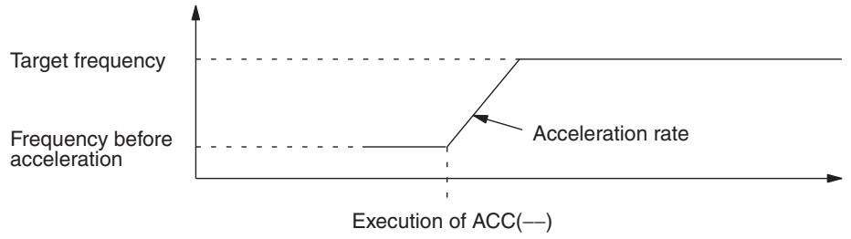
line
| Execution of ACC(—) | Target frequency | Frequency before acceleration | | ------------------- | ---------------- | ----------------------------- | | Low | High | Low | | Mid | High | Low | | High | High | Low |The 2 control words indicate the acceleration rate and target frequency.
1,2,3...
- The content of C determines the acceleration rate. During acceleration, the output frequency is increased by the amount set in C every 4.08 ms. C must be BCD from 0001 to 0200 (10 Hz to 2 kHz).
- The content of C+1 specifies the target frequency. C+1 must be BCD from 0000 to 5000 (0 Hz to 50 kHz).
Mode 2 (M=002)
Mode 2 is used to decrease the frequency being output to a target frequency at the specified rate. Output stops when the total number of pulses specified in PULS(65) have been output.
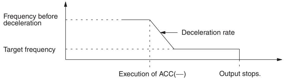
line
| Execution of ACC(—) | Deceleration rate | | ------------------- | ----------------- | | End | 0.8 | | Target frequency | 0.2 |The 2 control words indicate the deceleration rate and target frequency.
1,2,3...
- The content of C determines the deceleration rate. During deceleration, the output frequency is decreased by the amount set in C every 4.08 ms. C must be BCD from 0001 to 0200 (10 Hz to 2 kHz).
- The content of C+1 specifies the target frequency. C+1 must be BCD from 0000 to 5000 (0 Hz to 50 kHz).
Mode 3 (M=003)
Mode 3 is used to decrease the frequency being output to a target frequency at the specified rate. Pulse output continues until stopped.
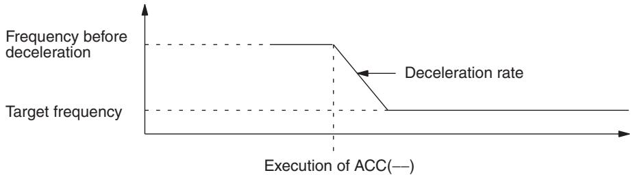
line
| Execution of ACC(—) | Target frequency | Deceleration rate | | ------------------- | ---------------- | ----------------- | | Low | High | High | | Mid | High | Decreasing | | High | Low | Decreasing |The 2 control words indicate the acceleration rate and target frequency.
1,2,3...
- The content of C determines the acceleration rate. During acceleration, the output frequency is increased by the amount set in C every 4.08 ms. C must be BCD from 0001 to 0200 (10 Hz to 2 kHz).
- The content of C+1 specifies the target frequency. C+1 must be BCD from 0000 to 5000 (0 Hz to 50 kHz).
Flags
ER: Indirectly addressed EM/DM word is non-existent.
(Content of *EM/*DM word is not BCD, or the EM/DM area boundary has been exceeded.)
There is an error in the operand settings.
ACC(—) is executed without a Pulse I/O Board installed.
The PC Setup is not set for pulse output.
ACC(—) is executed with M=000 and the specified output port is already in use.
ACC(—) is executed in an interrupt subroutine while a pulse I/O or high-speed counter instruction is being executed in the main program.
AR 0515: Port 1 output flag. ON when pulses are being output from port 1.
AR 0615: Port 2 output flag. ON when pulses are being output from port 2.
5-28-13 PULSE WITH VARIABLE DUTY FACTOR – PWM(—)
Ladder Symbols
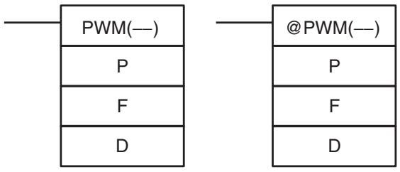
flowchart
graph TD
A["PWM(---)"] --> B["P"]
A --> C["F"]
A --> D["D"]
E["@PWM(---)"] --> F["P"]
E --> G["F"]
E --> H["D"]
Operand Data Areas
| P: Communications port |
| 001 or 002 |
| F: Frequency |
| 000, 001, or 002 |
| D: Duty factor |
| IR, SR, AR, DM, EM, HR, TIM/CNT, LR, # |
Limitations
PWM(—) cannot be used unless the PC Setup (DM 6643 or DM 6644) is set for variable duty factor pulse outputs.
P must be 001 or 002 and F must be 000, 001, or 002.
D must be BCD between 0001 and 0099.
Description
PWM(—) can be used with the functions listed in the following table.
| Unit/Board | Function |
| Pulse I/O Board | Pulse outputs 1 and 2 |
PWM(—) is used to output pulses with the specified duty factor from port 1 or 2. The output can be set to one of three frequencies: 5.9 kHz, 1.5 kHz, or 91.6 Hz. The pulse output continues until INI(61) is executed to stop it.
In order for PWM(—) to be executed, the specified port must be set for variable duty factor pulse outputs in the PC Setup. Set the leftmost digit of DM 6643 to 1 to enable variable duty factor pulse output from port 1, and set the leftmost digit of DM 6644 to 1 to enable variable duty factor pulse output from port 2. It is not possible to output normal pulses from a port that is set for variable duty factor output.
Note Refer to 1-5 Pulse Output Function for more details.
Operand Settings
P specifies the port where the pulses will be output. Pulses are output from port 1 when P=001, and pulses are output from port 2 when P=002.
F specifies the frequency of the pulse output, as shown in the following table.
| F | Frequency |
| 000 | 5.9 kHz |
| 001 | 1.5 kHz |
| 002 | 91.6 Hz |
D specifies the duty factor of the pulse output, i.e., the percentage of time that the output is ON. D must be BCD from 0001 to 0099 (1% to 99%). The duty factor is 75% in the following diagram.
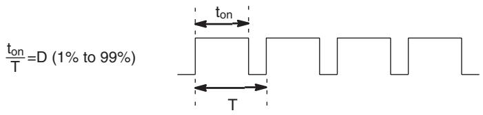
Flags
ER: There is an error in the operand settings.
PWM(—) is executed without a Pulse I/O Board installed.
The PC Setup is not set for variable duty factor pulse output.
PWM(—) is executed in an interrupt subroutine while a pulse I/O or high-speed counter instruction is being executed in the main program.
Indirectly addressed EM/DM word is non-existent.
(Content of *EM/*DM word is not BCD, or the EM/DM area boundary has been exceeded.)
5-28-14 DATA SEARCH – SRCH(—)
Ladder Symbols
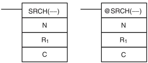
Operand Data Areas
| N: Number of words |
| IR, SR, AR, DM, EM, HR, TIM/CNT, LR, # |
| R1: First word in range |
| IR, SR, AR, DM, EM, HR, TIM/CNT, LR |
| C: Comparison data, result word |
| IR, SR, AR, DM, EM, HR, LR |
Limitations
N must be BCD between 0001 to 9999.
R_1 and R_1+N-1 must be in the same data area.
DM 6143 to DM 6655 cannot be used for C.
Description
When the execution condition is OFF, SRCH(—) is not executed. When the execution condition is ON, SRCH(—) searches the range of memory from R_1 to R_1+N-1 for addresses that contain the comparison data in C. If one or more addresses contain the comparison data, the EQ Flag (SR 25506) is turned ON and the lowest address containing the comparison data is identified in C+1. The address is identified differently for the DM area:
1,2,3...
- For an address in the DM area, the word address is written to C+1. For example, if the lowest address containing the comparison data is DM 0114, then #0114 is written in C+1.
- For an address in another data area, the number of addresses from the beginning of the search is written to C+1. For example, if the lowest address containing the comparison data is IR 114 and the first word in the search range is IR 014, then #0100 is written in C+1.
If none of addresses in the range contain the comparison data, the EQ Flag (SR 25506) is turned OFF and C+1 is left unchanged.
Flags
ER: Indirectly addressed EM/DM word is non-existent.
(Content of *EM/*DM word is not BCD, or the EM/DM area boundary has been exceeded.)
N is not BCD between 0001 and 9999.
EQ: ON when the comparison data has been matched in the search range.
Example
In the following example, the 10 word range from DM 0010 to DM 0019 is searched for addresses that contain the same data as DM 0000 (#FFFF). Since DM 0012 contains the same data, the EQ Flag (SR 25506) is turned ON and #0012 is written to DM 0001.
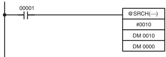
| Address | Instruction | Operands |
| 00000 | LD | 00001 |
| 00001 | @SRCH(—) | |
| # 0010 | ||
| DM 0010 | ||
| DM 0000 |
| DM 0010 | 0000 |
| DM 0011 | 9898 |
| DM 0012 | FFFF |
| DM 0013 | 9797 |
| DM 0014 | AAAA |
| DM 0015 | 9595 |
| DM 0016 | 1414 |
| DM 0017 | 0000 |
| DM 0018 | 0000 |
| DM 0019 | FFFF |
| DM 0000 | FFFF |
| DM 0001 | 0012 |
5-28-15 PID CONTROL – PID(—)
Ladder Symbol
| PID(---) |
| IW |
| P1 |
| OW |
Operand Data Areas
| IW: Input data word |
| IR, SR, AR, DM, EM, HR, LR |
| P1: First parameter word |
| IR, SR, DM, EM, HR, LR |
| OW: Output data word |
| IR, SR, AR, DM, EM, HR, LR |
Limitations
DM 6144 to DM 6655 cannot be used for IW, P1 to P1+32, or OW.
P1 to P1+32 must be in the same data area.
Caution
A total of 33 continuous words starting with P1 must be provided for PID(—) to operate correctly. Also, PID(—) may not operate dependably in any of the following situations: In interrupt programs, in subroutines, between IL(02) and ILC(03), between JMP(04) and JME(05), and in step programming (STEP(08)/SNXT(09)). Do not program PID(—) in these situations.
Description
PID(—) performs PID control based on the parameters specified in P1 through P1+6. The data in IW is used to calculate the output data that is written to OW. The following table shows the function of the parameter words.
| Word | Bits | Parameter name | Function/Setting range |
| P1 | 00 to 15 | Set value (SV). | This is the target value for PID control. It can be set to any binary number with the number of bits set by the input range parameter. |
| P1+1 | 00 to 15 | Proportional band width. | This parameter specifies the proportional band width/input range ratio from 0.1% to 999.9%. It must be BCD from 0001 to 9999. |
| P1+2 | 00 to 15 | Integral time | Sets the integral time/sampling period ratio used in integral control. It must be BCD from 0001 to 8191, or 9999. (9999 disables integral control.) |
| P1+3 | 00 to 15 | Derivative time | Sets the derivative time/sampling period ratio used in derivative control. It must be BCD from 0001 to 8191, or 0000. |
| P1+4 | 00 to 15 | Sampling period | Sets the interval between samplings of the input data from 0.1 to 102.3 s. It must be BCD from 0001 to 1023. |
| P1+5 | 00 to 03 | Operation specifier | Sets reverse or normal operation. Set to 0 to specify reverse operation or 1 to specify normal operation. |
| 04 to 15 | Input filter coefficient | Determines the strength of the input filter. The lower the coefficient, the weaker the filter.This setting must be BCD from 100 to 199, or 000. A setting of 000 sets the default value (0.65) and a setting of 100 to 199 sets the coefficient from 0.00 to 0.99. | |
| P1+6 | 00 to 07 | Output range | Determines the number of bits of output data. This setting must be between 00 and 08, which sets the output range between 8 and 16 bits. |
| 08 to 15 | Input range | Determines the number of bits of input data. This setting must be between 00 and 08, which sets the input range between 8 and 16 bits. | |
| P1+7 to P1+32 | 00 to 15 | Work area | Do not use.(Used by the system.) |
When the execution condition is OFF, PID(—) is not executed and the instruction's data is maintained. While the execution condition is OFF, the desired output data can be written directly to OW for manual control.
When the execution condition first goes from OFF to ON, PID(—) reads the parameters and initializes the work area. There is a built-in function to change the output data continuously at startup because sudden changes in the output data might adversely affect the controlled system.

Changes made to the parameters will not be effective until the execution condition for PID(—) goes from OFF to ON.
Note Do not use PID(—) in the following situations; it may not be executed properly. In interrupt programs
In subroutine programs
In interlocked program sections (between IL and ILC)
In jump program sections (between JMP and JME)
In step ladder program section (created with STEP)
When the execution condition is ON, PID(—) performs the PID calculation on the input data when the sampling period has elapsed. The sampling period is the time that must pass before input data is read for processing.
The following diagram shows the relationship between the sampling period and PID processing. PID processing is performed only when the sampling period (100 ms in this case) has elapsed.
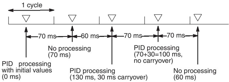
Flags
ER: There is an error in the parameter settings.
The cycle time is more than twice as long as the sampling period, so PID(—) cannot be executed accurately. PID(—) will be executed in this case.
Indirectly addressed EM/DM word is non-existent.
(Content of *EM/*DM word is not BCD, or the EM/DM area boundary has been exceeded.)
CY: ON when PID processing has been performed. (OFF when the sampling period has not elapsed.)
5-29 Network Instructions
The network instructions are used for communicating with other PCs host computers linked through the Controller Link System.
5-29-1 NETWORK SEND – SEND(90)
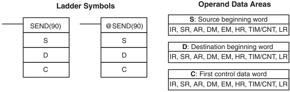
Limitations
C through C+2 must be within the same data area and must be within the values specified below. To be able to use SEND(90), the system must have a Controller Link Unit mounted.
Description
When the execution condition is OFF, SEND(90) is not executed. When the execution condition is ON, SEND(90) transfers data beginning at word S, to addresses specified by D in the designated node on the Controller Link System. The control words, beginning with C, specify the number of words to be sent, the destination node, and other parameters.
Control Words
SEND(90) transmits “n” words beginning with S (the beginning source word for data transmission at the source node) to the “n” words beginning with D (the beginning destination word for data reception at destination node N).
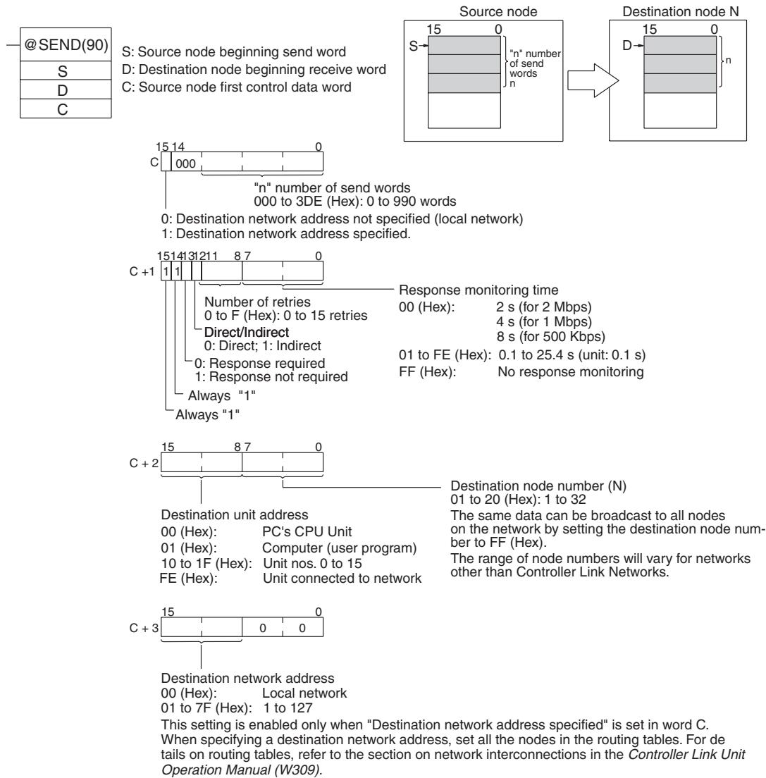
Executing SEND(90) just starts the data transmission via the Communications Unit. To check whether the transmission was actually completed, verify that the Network Instruction Enabled Flag (AR 0209) has gone from OFF to ON and the Network Instruction Error Flag (AR 0208) is OFF. The transmission processing is completed when END(01) is executed.
If a response is required but not received within the response monitoring time, the data transmission will be retried until a response is received or the specified number of retries (up to 15) is reached.
When the destination node number is set to FF, the same data will be broadcast to all nodes on the specified network. When broadcast transmission is specified, responses will not be returned and transmissions will not be retried.
If the Network Instruction Enabled Flag (AR 0209) is OFF when SEND(90) is executed, the instruction will be treated as NOP(00) and won't be executed. An error will occur and the Error Flag will be turned ON.
If the Network Instruction Enabled Flag (AR 0209) is ON when SEND(90) is executed, the Network Instruction Error Flag (AR 0208) and Network Instruction Enabled Flag (AR 0209) will be turned OFF, the Network Instruction Completion Code will be set to 00, and the data will be sent to the node(s) on the network.
When a current-bank EM area address is specified for the destination beginning word (D), the transmitted data will be written to the destination node's current EM bank. Indirect addressing can be used for the destination beginning word (D) when transmitting to PCs that have larger data areas than the CQM1H such as the CS1-series or CV-series PCs. Indirect addressing can also be used to change the destination beginning word to suit the circumstances.
If data will be transmitted to nodes in other networks, routing tables must be registered in the PCs (CPU Units) in each network. (Routing tables indicate the routes to other networks in which destination nodes are connected.)
Only one network instruction may be executed at one time. To ensure that a second network instruction isn't executed until the first is completed, program the Network Instruction Enabled Flag (AR 0209) as a normally open condition.
Never change the control data (C through C+3) while data is being transmitted and the Network Instruction Enabled Flag is OFF.
Noise and other factors can cause the transmission or response to be corrupted or lost, so we recommend setting the number of retries to a non-zero value which will cause SEND(90) to be executed again if the response is not received within the response monitoring time.
Indirect Destination Beginning Word Designations
D is used to specify the destination beginning word as follows when indirect specification is designated:
| Word | Bits 12 to 15 | Bits 08 to 11 | Bits 04 to 07 | Bits 00 to 03 |
| D | Area type | 0 | Word address (5th digit) | |
| D+1 | Word address (4th digit) | Word address (3rd digit) | Word address (2nd digit) | Word address (1st digit) |
CS1-series PCs and CV-series PCs have larger data areas than CQM1H, so the beginning words for sending and receiving at destination nodes cannot always be directly specified by means of SEND(90) and RECV(98) operands. Moreover, depending on circumstances, it may be desirable to change the beginning word at destination nodes.
In such cases, set the “Direct/Indirect” control data designation to “1” (Indirect), and specify the beginning words for sending as described below.
The beginning receive word is determined by the contents of the destination node's D and D+1 words.
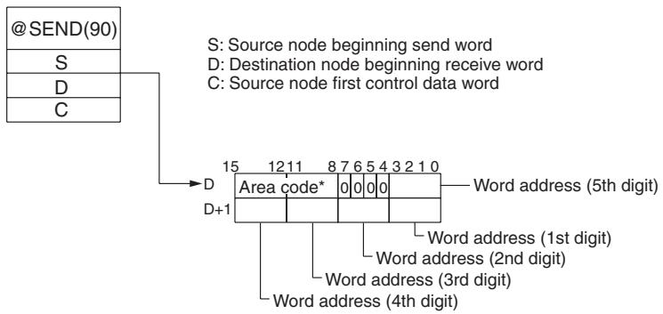
Note Specify the area code according to the following table.
| Destination node:CS1-series PC | Destination node:CQM1H, C200HX/HG/HE PC | Destination node:CV-series PC | ||||||
| Area | Code | Area | Code | Area | Code | |||
| CIO | 00 | IR | 00 | CIO | 00 | |||
| Timer (see note 1) | 03 | LR | 06 | CPU Bus Link | 01 | |||
| Counter (see note 2) | 04 | HR | 07 | Auxiliary | 02 | |||
| DM | 05 | AR | 08 | Timer | 03 | |||
| EM | Banks 0 to 7Banks 8 to 15Current bank | 10 to 17A8 to AC18 | Timer/Counter | 03 | Counter | 04 | ||
| DM | 05 | DM | 05 | |||||
| EM | Banks 0 to 7Banks 8 to 15Current bank | 10 to 1728 to 2F18 | EM | Banks 0 to 7Current bank | 10 to 1718 | |||
Note
- Words 0 to 2555 in the IR Area can send and receive data.
- Timer/counter numbers 0 to 2047 can send and receive data.
Examples
When IR 00000 and AR 0209 (the Network Instruction Enabled Flag) are ON in the following example, the ten words from DM 0100 to DM 0109 are transmitted to node number 3 in the local network where they are written to the ten words from DM 0200 to DM 0209. The data will be retransmitted up to 3 times if a response is not received within ten seconds.
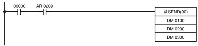
| Address | Instruction | Operands | |
| 00000 | LD | 00000 | |
| 00001 | AND | AR | 0209 |
| 00002 | SEND(90) | ||
| DM | 0100 | ||
| DM | 0200 | ||
| DM | 0300 | ||
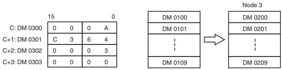
Flags
ER: Indirectly addressed EM/DM word is non-existent.
(Content of *EM/*DM word is not BCD, or the EM/DM area boundary has been exceeded.)
The number of send words exceeds 990 words for a Controller Link Unit.
There is no Controller Link Unit installed.
The source words exceed the data area boundary.
5-29-2 NETWORK RECEIVE - RECV(98)
Ladder Symbols
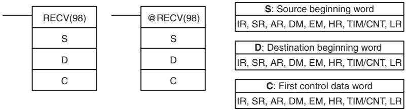
flowchart
graph TD
A["RECV(98)"] --> B["S"]
A --> C["D"]
A --> D["C"]
E["@RECV(98)"] --> F["S"]
E --> G["D"]
E --> H["C"]
I["S: Source beginning word"] --> J["IR, SR, AR, DM, EM, HR, TIM/CNT, LR"]
K["D: Destination beginning word"] --> L["IR, SR, AR, DM, EM, HR, TIM/CNT, LR"]
M["C: First control data word"] --> N["IR, SR, AR, DM, EM, HR, TIM/CNT, LR"]
Limitations
C through C+2 must be within the same data area and must be within the values specified below. To be able to use RECV(98), the system must have a Controller Link Unit mounted.
Description
When the execution condition is OFF, RECV(98) is not executed. When the execution condition is ON, RECV(98) transfers data beginning at S from a node on the Controller Link System to words beginning at D. The control words, beginning with C, provide the number of words to be received, the source node, and other transfer parameters.
Control Words
RECV(98) receives “m” words beginning with S (the beginning word for data transmission at the destination node, M) to the words from D (the beginning word for data reception at the source node) onwards.
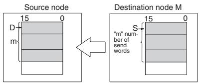
| -@RECV(98) |
| S |
| D |
| C |
S: Destination node beginning send word
D: Source node beginning receive word
C: Source node first control data word
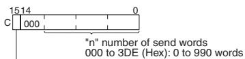
0: Source network address not specified (local network) 1: Source network address specified.
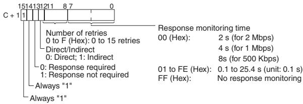
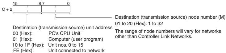
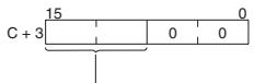
Destination network address
00 (Hex): Local network
01 to 7F (Hex): 1 to 127
This setting is enabled only when "Destination network address specified" is set in word C.
When specifying the destination network address, set all the nodes in the routing tables. For
details on the routing tables, refer to the section on network interconnections in the Controller
Link Unit Operation Manual (W309).
Executing RECV(98) just starts the data reception via the Communications Unit. To check whether the reception was actually completed, verify that the Network Instruction Enabled Flag (AR 0209) has gone from OFF to ON and the Network Instruction Error Flag (AR 0208) is OFF. The reception processing is completed when END(01) is executed.
A response is required with RECV(098) because the response contains the data being received, so set bit 13 of C+1 to "0" to indicate that a response is required. If the response hasn't been received within the response monitoring time set in C+4, the request for data transfer will be retransmitted until a response is received or the specified number of retries (up to 15) is reached.
If the Network Instruction Enabled Flag (AR 0209) is OFF when RECV(98) is executed, the instruction will be treated as NOP(00) and won't be executed. An error will occur and the Error Flag will be turned ON.
If the Network Instruction Enabled Flag (AR 0209) is ON when RECV(98) is executed, the Network Instruction Error Flag (AR 0208) and Network Instruction Enabled Flag (AR 0209) will be turned OFF, the Network Instruction Completion Code will be set to 00, and the data will be received from the other node.
Only one network instruction may be executed at one time. To ensure that a second network instruction isn't executed until the first is completed, program the Network Instruction Enabled Flag (AR 0209) as a normally open condition.
Never change the control data (C through C+3) while data is being received and the Network Instruction Enabled Flag is OFF.
Noise and other factors can cause the request for transfer or response to be corrupted or lost, so we recommend setting the number of retries to a non-zero value which will cause RECV(98) to be executed again if the response is not received within the response monitoring time.
Indirect addressing can be used for the source beginning word (S) when receiving data from PCs that have larger data areas than the CQM1H such as the CS1-series or CV-series PCs. Indirect addressing can also be used to change the source beginning word to suit the circumstances.
Indirect Source Beginning Word Designations
S is used to specify the source beginning word when indirect specification is required. Use the same designations as those used for the destination beginning word for SEND(90).
Examples
When IR 00000 and AR 0209 (the Network Instruction Enabled Flag) are ON in the following example, the data in ten words from DM 0100 to DM 0109 in node number 3 in the local network is received and written to the ten words from DM 0200 to DM 0209. The request for data transfer will be retransmitted up to 3 times if a response is not received within ten seconds.
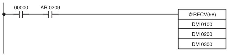
| Address | Instruction | Operands | |
| 00000 | LD | 00000 | |
| 00001 | AND | AR | 0209 |
| 00002 | RECV(98) | ||
| DM | 0100 | ||
| DM | 0200 | ||
| DM | 0300 | ||
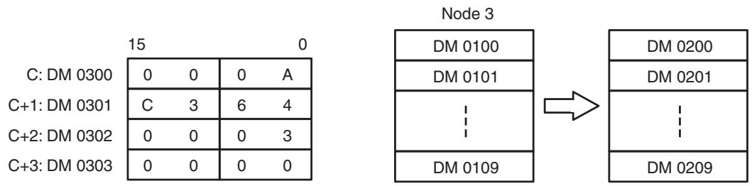
flowchart
graph LR
subgraph Node 3
direction TB
A["DM 0100"] --> B["DM 0101"]
B --> C["..."]
C --> D["DM 0109"]
E["DM 0200"] --> F["DM 0201"]
G["DM 0209"]
end
subgraph C
H["C: DM 0300"] --> I["0 0 0 A"]
J["C+1: DM 0301"] --> K["C 3 6 4"]
L["C+2: DM 0302"] --> M["0 0 0 3"]
N["C+3: DM 0303"] --> O["0 0 0 0"]
end
Flags
ER: Indirectly addressed EM/DM word is non-existent.
(Content of *EM/*DM word is not BCD, or the EM/DM area boundary has been exceeded.)
The number of send words exceeds 990 words for a Controller Link Unit.
There is no Controller Link Unit installed.
The received data exceeds the data area boundary.
5-29-3 DELIVER COMMAND: CMND(—)
Ladder Symbols
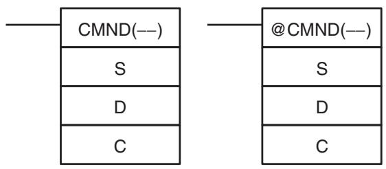
Operand Data Areas
| S: First command word |
| IR, SR, AR, DM, EM, HR, TIM/CNT, LR |
| D: First response word |
| IR, SR, AR, DM, EM, HR, TIM/CNT, LR |
| C: First control word |
| IR, SR, AR, DM, EM, HR, TIM/CNT, LR |
Limitations
C through C+5 must be within the same data area and must be within the values specified below. To be able to use CMND(—), the system must have a Controller Link Unit mounted.
Description
When the execution condition is OFF, CMND(—) is not executed. When the execution condition is ON, CMND(—) transmits the FINS command beginning at word S to the specified node on the Controller Link System and receives the response.
flowchart
graph LR
subgraph Local node
S["15"] --> S
S --> D["15"]
D --> S
S --> Command["Command data (n bytes)"]
D --> Response["Response data (m bytes)"]
end
subgraph Destination node
Interpret["Interpret"]
Execute["Execute"]
end
S -->|Command| Destination node
D -->|Response| Destination node
Control Words
The six control words C to C+5 specify the number of bytes of command data and response data, the destination, and other settings shown in the following table.
| Word | Bits 00 to 07 | Bits 08 to 15 |
| C | Bytes of command data: 0000 to 07C6 hexadecimal (0 to 1,990 bytes) | |
| C+1 | Bytes of response data: 0000 to 07C6 hexadecimal (0 to 1,990 bytes) | |
| C+2 | Destination network address00: Local network01 to 7F: Network 1 to 127 | Always 00. |
| C+3 | Destination unit address00: CPU Unit01: Computer (user program)10 to 1F: Units 0 to 15E1: Inner BoardFE: Unit connected to network | Destination node number01 to 20: 1 to 32 (See note 1.)FF: Broadcast (See note 2.) |
| C+4 | No. of retries: 00 to 0F (0 to 15) | Response setting00: Response requested.80: No response requested. |
| C+5 | Response monitoring time0000: 2 s at 2 Mbps, 4 s at 1 Mbps, or 8 s at 500 Kbps0001 to FFFF: 0.1 to 6,553.5 seconds (0.1 s units) | |
Note
- The allowed range is 01 to 20 hexadecimal (1 to 32) for a Controller Link, but the maximum node number will differ for other networks.
- Set the destination node number to FF to broadcast the command to all nodes in the network.
Executing CMND(—) just starts the transmission of the FINS command via the Communications Unit. To check whether the transmission was actually completed, verify that the Network Instruction Enabled Flag (AR 0209) has gone from OFF to ON and the Network Instruction Error Flag (AR 0208) is OFF. The command transmission processing is completed when END(01) is executed.
If a response is required but not received within the response monitoring time, the command will be issued again until a response is received or the specified number of retries (up to 15) is reached. Be sure to indicate that no response is required when issuing command does not generate a response.
When the destination node number is set to FF, the same command will be broadcast to all nodes on the specified network. When broadcast transmis-
sion is specified, responses will not be returned and transmissions will not be retried.
An error will occur if the amount of response data exceeds the number of bytes of response data set in C+1.
If the Network Instruction Enabled Flag (AR 0209) is OFF when CMND(—) is executed, the instruction will be treated as NOP(00) and won't be executed. An error will occur and the Error Flag will be turned ON.
If the Network Instruction Enabled Flag (AR 0209) is ON when CMND(—) is executed, the Network Instruction Error Flag (AR 0208) and Network Instruction Enabled Flag (AR 0209) will be turned OFF, the Network Instruction Completion Code will be set to 00, and the FINS command will be issued to the node(s) on the network.
The destination node(s) will be located through the routing tables registered in the network PCs. (Routing tables indicate the routes to other networks in which destination nodes are connected.)
Only one network instruction may be executed at one time. To ensure that a second network instruction isn't executed until the first is completed, program the Network Instruction Enabled Flag (AR 0209) as a normally open condition.
Never change the control data (C through C+5) while FINS command is being processed and the Network Instruction Enabled Flag is OFF.
Noise and other factors can cause the transmission or response to be corrupted or lost, so we recommend setting the number of retries to a non-zero value which will cause CMND(—) to be executed again if the response is not received within the response monitoring time.
CMND(—) operates just like SEND(90) if the FINS command code is 0102 (MEMORY AREA WRITE) and just like RECV(098) if the code is 0101 (MEMORY AREA READ).
Examples
When IR 00000 and AR 0209 (the Network Instruction Enabled Flag) are ON in the following example, CMND issues FINS command 0101 (MEMORY AREA READ) to node number 3 in the local network.
The MEMORY AREA READ command reads 10 words from DM 0010 to DM 0019. The response contains the 2-byte command code (0101), the 2-byte completion code, and then the 10 words of data, for a total of 12 words or 24 bytes.
The command will be issued again up to 3 times if a response is not received within ten seconds.
| Address | Instruction | Operands |
| 00000 | LD | 00000 |
| 00001 | AND | AR 0209 |
| 00002 | SEND(90) | |
| DM 0100 | ||
| DM 0200 | ||
| DM 0300 |
other
| S/DM | 15 | 0 | Command code: 0101 hexadecimal (MEMORY AREA READ) | DM 0010 (Data area = 82 hexadecimal, address = 000A00) | Number of words to read = 0A hexadecimal (10 decimal) | | :--- | :--- | :--- | :--- | :--- | :--- | | S: DM 0100 | 0 | 1 | | | | | S+1: DM 0101 | 8 | 2 | | | | | S+2: DM 0102 | 0 | A | | | | | S+3: DM 0103 | 0 | 0 | | | | Command code: 0101 hexadecimal (MEMORY AREA READ)
other
| Category | 15 | 0 | Bytes of command data: 0008 (8 decimal) | Bytes of response data: 0018 (24) | Transmit to the local network and the device itself | Node number 3, unit address 00 (CPU Unit) | Response requested, port number 0, 3 retries | Response monitoring time: 0064 hexadecimal (10 seconds) | | :--- | :--- | :--- | :--- | :--- | :--- | :--- | :--- | :--- | | C: DM 0300 | 0 | 0 | 0 | 8 | | | | | | C+1: DM 0301 | 0 | 0 | 1 | 8 | | | | | | C+2: DM 0302 | 0 | 0 | 0 | 0 | | | | | | C+3: DM 0303 | 0 | 3 | 0 | 0 | | | | | | C+4: DM 0304 | 0 | 0 | 0 | 3 | | | | | | C+5: DM 0305 | 0 | 0 | 6 | 4 | | | | | The values in the table represent the byte values for each data type. The byte values are annotated above the cells.Flags
ER: Indirectly addressed EM/DM word is non-existent.
(Content of *EM/*DM word is not BCD, or the EM/DM area boundary has been exceeded.)
5-30 Communications Instructions
5-30-1 RECEIVE - RXD(47)
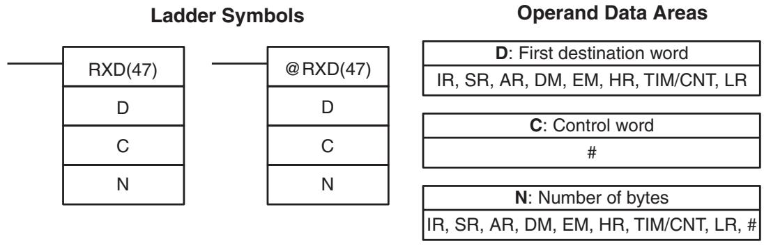
Limitations
D and D+(N÷2)-1 must be in the same data area.
DM 6144 to DM 6655 cannot be used for D or N.
N must be BCD from #0000 to #0256.
Description
When the execution condition is OFF, RXD(47) is not executed. When the execution condition is ON, RXD(47) reads N bytes of data received at the port specified in the control word, and then writes that data in words D to D+(N÷2)-1. Up to 256 bytes of data can be read at one time.
If fewer than N bytes are received, the amount received will be read.
Note Refer to 1-6 Communications Functions for more details on using the RXD(47) instruction, setting communications protocol in the PC Setup, etc.
The CQM1H will be incapable of receiving more data once 256 bytes have been received if received data is not read using RXD(47). Read data as soon as possible after the Reception Completed Flag is turned ON. The following table lists the Reception Completed Flags for the various ports.
| Port | Reception Completed Flag | |
| CPU Unit's built-in RS-232C port | AR 0806 | |
| Peripheral port | AR 0814 | |
| Serial Communications Board | Port 1 | IR 20106 |
| Port 2 | IR 20114 | |
Communications flags and counters can be cleared by executing RXD(47) with N set to 0000.
Related Flags and Control Bits
The following table lists the various flags, control bits, and words that are used when receiving data with RXD(47).
| Port | Flag | Function |
| CPU Unit's built-in RS-232C port | AR 0806 | The Reception Completed Flag is turned ON when reception is completed and is turned OFF after data is read with RXD(47). |
| AR 09 | Contains the number of bytes received in 4-digit BCD. This word is cleared to 0000 after data is read with RXD(47). | |
| SR 25209 | Turn ON the RS-232C Port Reset Bit to reset the RS-232C port. | |
| Peripheral port | AR 0814 | The Reception Completed Flag is turned ON when reception is completed and is turned OFF after data is read with RXD(47). |
| AR 10 | Contains the number of bytes received in 4-digit BCD. This word is cleared to 0000 after data is read with RXD(47). | |
| SR 25208 | Turn ON the Peripheral Port Reset Bit to reset the peripheral port. | |
| Serial Communications Board port 1 | IR 20106 | The Reception Completed Flag is turned ON when reception is completed and is turned OFF after data is read with RXD(47). |
| IR 202 | Contains the number of bytes received in 4-digit BCD. This word is cleared to 0000 after data is read with RXD(47). | |
| IR 20700 | Turn ON the Port 1 Restart Bit to reset port 1. | |
| Serial Communications Board port 2 | IR 20114 | The Reception Completed Flag is turned ON when reception is completed and is turned OFF after data is read with RXD(47). |
| IR 203 | Contains the number of bytes received in 4-digit BCD. This word is cleared to 0000 after data is read with RXD(47). | |
| IR 20701 | Turn ON the Port 2 Restart Bit to reset port 2. |
Control Word (C)
The value of the control word determines the port from which data will be read and the order in which data will be written to memory.

flowchart
graph TD
A["Digit number: 3 2 1 0"] --> B["Byte order 0: Most significant bytes first"]
A --> C["Not used. (Set to 0.)"]
A --> D["Serial port specifier (when bits 12 to 15 are 0.)"]
A --> E["Port 0: Port other than the peripheral port"]
B --> F["1: Least significant bytes first"]
C --> G["0: CPU Unit's built-in RS-232C port"]
D --> H["1: Serial Communications Board port 1"]
D --> I["2: Serial Communications Board port 2"]
E --> J["1: Peripheral port"]
The order in which data is written to memory depends on the value of digit 0 of C. Eight bytes of data 12345678... will be written in the following manner:
Digit 0 = 0
| MSB LSB | ||
| D | 1 | 2 |
| D+1 | 3 | 4 |
| D+2 | 5 | 6 |
| D+3 | 7 | 8 |
| | | | | | |
| | | | | | |
| | | | | | |
Digit 0 = 1
| MSB LSB | ||
| D | 2 | 1 |
| D+1 | 4 | 3 |
| D+2 | 6 | 5 |
| D+3 | 8 | 7 |
| | | | | | |
| | | | | | |
| | | | | | |
Flags
ER: A port on the Serial Communications Board is specified, but a Serial Communications Board is not installed.
There is an error in the communications settings (PC Setup) or the operand settings.
Indirectly addressed EM/DM word is non-existent.
(Content of *EM/*DM word is not BCD, or the EM/DM area boundary has been exceeded.)
The destination words (D to D+(N÷2)-1) exceed the data area.
5-30-2 TRANSMIT - TXD(48)
Ladder Symbols
| TXD(48) | @TXD(48) |
| S | S |
| C | C |
| N | N |
Operand Data Areas
| S: First source word |
| IR, SR, AR, DM, EM, HR, TIM/CNT, LR |
| C: Control word |
| # |
| N: Number of bytes |
| IR, SR, AR, DM, EM, HR, TIM/CNT, LR, # |
Limitations
S and S+(N÷2)-1 must be in the same data area.
DM 6144 to DM 6655 cannot be used for S or N.
N must be BCD from #0000 to #0256. (#0000 to #0061 in host link mode)
Description
When the execution condition is OFF, TXD(48) is not executed. When the execution condition is ON, TXD(48) reads N bytes of data from words S to S+(N÷2)-1 , converts it to ASCII, and outputs the data from the specified port.
TXD(48) operates differently in host link mode and no-protocol mode, so these modes are described separately.
Note Refer to 1-6 Communications Functions for more details on using the TXD(48) instruction, setting communications protocol in the PC Setup, etc.
Host Link Mode
N must be BCD from #0000 to #0061 (i.e., up to 122 bytes of ASCII). The value of the control word (C) determines the port from which data will be output, as shown below.
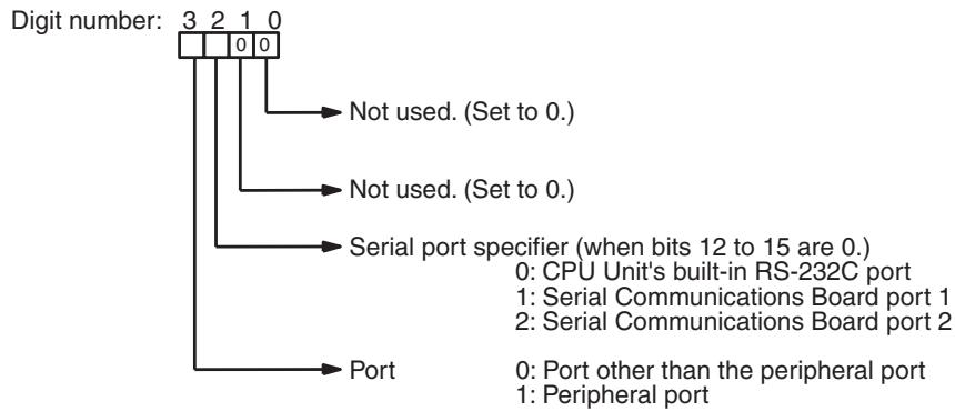
flowchart
graph TD
A["Digit number: 3 2 1 0"] --> B["Not used. (Set to 0.)"]
A --> C["Not used. (Set to 0.)"]
A --> D["Serial port specifier (when bits 12 to 15 are 0.)"]
D --> E["0: CPU Unit's built-in RS-232C port"]
D --> F["1: Serial Communications Board port 1"]
D --> G["2: Serial Communications Board port 2"]
A --> H["Port"]
H --> I["0: Port other than the peripheral port"]
H --> J["1: Peripheral port"]
The specified number of bytes will be read from S through S+(N/2)-1, converted to ASCII, and transmitted through the specified port. The bytes of source data shown below will be transmitted in this order: 12345678...
| MSB | LSB | |
| S | 1 | 2 |
| S+1 | 3 | 4 |
| S+2 | 5 | 6 |
| S+3 | 7 | 8 |
| | | | | | |
| | | | | | |
| | | | | | |
The following table lists the Transmission Enabled Flags for each port. The corresponding Transmission Enabled Flag will be ON when the CQM1H is capable of transmitting data through that port.
| Port | Transmission Enabled Flag | |
| CPU Unit's built-in RS-232C port | AR 0805 | |
| Peripheral port | AR 0813 | |
| Serial Communications Board | Port 1 | IR 20105 |
| Port 2 | IR 20113 | |
The following diagram shows the format for host link command (TXD) sent from the CQM1H. The CQM1H automatically attaches the prefixes and suffixes, such as the node number, header, and FCS.
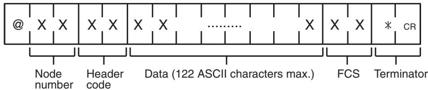
No-protocol Mode
N must be BCD from #0000 to #00256. The value of the control word determines the port from which data will be output and the order in which data will be written to memory.
Control Word (C)
The value of the control word determines the port from which data will be read and the order in which data will be written to memory.
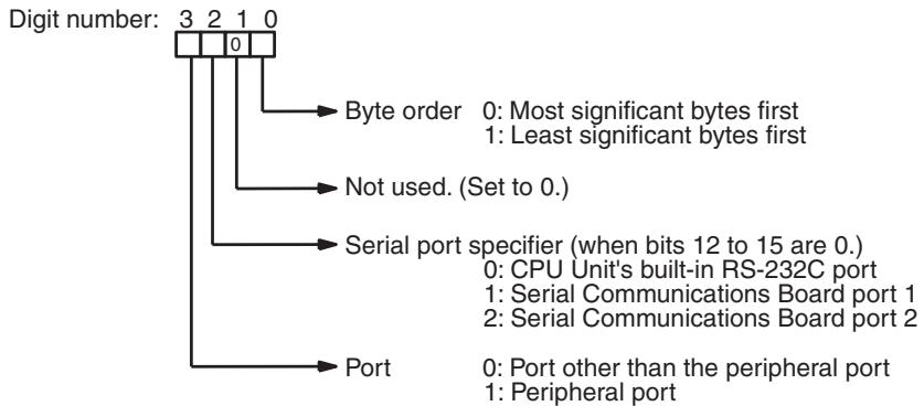
flowchart
graph TD
A["Digit number: 3 2 1 0"] --> B["Byte order 0: Most significant bytes first\n1: Least significant bytes first"]
A --> C["Not used. (Set to 0.)"]
A --> D["Serial port specifier (when bits 12 to 15 are 0.)\n0: CPU Unit's built-in RS-232C port\n1: Serial Communications Board port 1\n2: Serial Communications Board port 2"]
A --> E["Port 0: Port other than the peripheral port\n1: Peripheral port"]
The specified number of bytes will be read from S through S+(N÷2)-1 and transmitted through the specified port.
| MSB | LSB | |
| S | 1 | 2 |
| S+1 | 3 | 4 |
| S+2 | 5 | 6 |
| S+3 | 7 | 8 |
| | | | | | |
| | | | | | |
| | | | | | |
When digit 0 of C is 0, the bytes of source data shown above will be transmitted in this order: 12345678...
When digit 0 of C is 1, the bytes of source data shown above will be transmitted in this order: 21436587...
Note When start and end codes are specified the total data length should be 256 bytes max., including the start and end codes. (The maximum data length is 254 bytes when both a start code and end code are specified.)
Flags
ER: A port on the Serial Communications Board is specified, but a Serial Communications Board is not installed.
There is an error in the communications settings (PC Setup) or the operand settings.
Indirectly addressed EM/DM word is non-existent.
(Content of *EM/*DM word is not BCD, or the EM/DM area boundary has been exceeded.)
The source words (S to S+(N÷2)-1) exceed the data area.
5-30-3 CHANGE SERIAL PORT SETUP - STUP(—)
Ladder Symbols
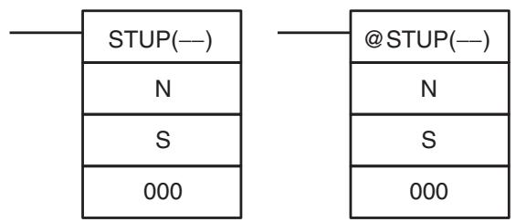
Operand Data Areas
| N: Port specifier |
| IR 000, IR 001, IR 002, or IR 003 |
| S: First source word |
| IR, SR, AR, DM, EM, HR, TIM/CNT, LR, # |
| Third operand: Set to 000. |
| - |
Limitations
N must be IR 000, IR 001, IR 002, or IR 003.
S and S+4 must be in the same data area.
(S can be set to #0000 to change the RS-232C settings to their defaults.)
STUP(—) cannot be executed for the CPU Unit's built-in RS-232C port if pin 5 on the DIP switch is ON.
STUP(—) cannot be executed within an interrupt subroutine.
Description
When the execution condition is OFF, STUP(—) is not executed. When the execution condition is ON, STUP(—) changes the PC Setup settings for the port specified by N.
N determines which part of the RS-232C Setup is changed.
| N | Specified Port |
| IR 000 | Built-in RS-232C port (PC Setup: DM 6645 to DM 6649) |
| IR 001 | Serial Communications Board port 1 (PC Setup: DM 6555 to DM 6559) |
| IR 002 | Serial Communications Board port 2 (PC Setup: DM 6550 to DM 6554) |
| IR 003 | Peripheral port (PC Setup: DM 6650 to DM 6654) |
If S is a word address, the contents of S through S+4 are copied to the 5 words in the PC Setup that contain the settings for the port specified by N.
If S is input as the constant #0000, the settings for the specified port are reset to their default values.
| S | Function |
| Word address | The contents of S through S+4 are copied to the part of the PC Setup that contains the settings for the port specified by N. |
| Constant (#0000) | The settings for the port specified by N are reset to their default values. |
The following table lists the Settings Changing Flags or Protocol Macro Executing Flags for each port. The corresponding flag will remain ON while STUP(—) is being executed and will be turned OFF when the change has been completed.
| Port | Flag name | Flag address | |
| Built-in RS-232C port | CPU Unit RS-232C Port Settings Changing Flag | AR 2404 | |
| Peripheral port | CPU Unit Peripheral Port Settings Changing Flag | AR 2403 | |
| Serial Communications Board | Port 1 | Protocol Macro Executing Flag | IR 20708 |
| Port 2 | Protocol Macro Executing Flag | IR 20712 | |
Application Example
This example shows a program that transfers the contents of DM 0100 through DM 0104 to the PC Setup area for Serial Communications Board port 1 (DM 6555 through DM 6559) when IR 00000 is ON and IR 20708 is OFF.
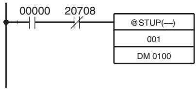
| Address | Instruction | Operands |
| 00000 | LD | 00000 |
| 00001 | AND NOT | 20708 |
| 00002 | @STUP(—) | |
| 001 | ||
| DM 0100 |
The settings are transferred as shown below. The Port 1 Protocol Macro Executing Flag (IR 20708) will be turned OFF again when the transfer has been completed.
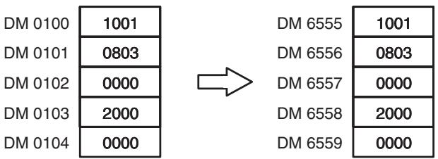
The following table shows the function of the transferred setup data.
| Word | Content | Function |
| DM 0100 | 1001 | Enables the communications settings in DM 0101 and sets the communications mode to RS-232C. |
| DM 0101 | 0803 | Sets the following communications settings:9,600 bps, 1 start bit, 8-bit data, 1 stop bit, no parity |
| DM 0102 | 0000 | No transmission delay (0 ms) |
| DM 0103 | 2000 | Enables the end code CR, LF. |
| DM 0104 | 0000 | --- |
Note An error will occur if STUP(—) is executed while a port's Settings Changing Flag or Protocol Macro Executing Flag is ON, so include the flag as a normally closed execution condition.
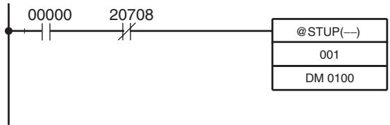
Use STUP(—) to change settings such as the communications mode during operation. For example, a communications sequence can be executed in Protocol Macro mode to exchange data through a modem connection and the communications mode can be switched to Host Link mode when necessary to monitor/program the PC without stopping operation.
Flags
ER: Indirectly addressed EM/DM word is non-existent.
(Content of *EM/*DM word is not BCD, or the EM/DM area boundary has been exceeded.)
The port specifier (N) isn't IR 000, IR 001, IR 002, or IR 003.
The specified source words exceed the data area.
The built-in RS-232C port or the peripheral port has been specified, but pin 5 on the DIP switch is ON.
A port on the Serial Communications Board is specified, but a Serial Communications Board is not installed.
STUP(—) was executed when the specified port's Settings Changing Flag (AR 2404 for the RS-232C port or AR 2403 for the peripheral port) or Protocol Macro Executing Flag (IR 20708 for port 1 or IR 20712 for port 2) was ON.
5-30-4 PROTOCOL MACRO - PMCR(—)
Ladder Symbols
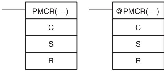
flowchart
graph TD
A["PMCR(—)"] --> B["C"]
A --> C["S"]
A --> D["R"]
E["@PMCR(—)"] --> F["C"]
E --> G["S"]
E --> H["R"]
Operand Data Areas
| C: Control word |
| IR, SR, AR, DM, EM, HR, TIM/CNT, LR, # |
| S: First send word |
| IR, SR, AR, DM, EM, HR, TIM/CNT, LR, # |
| R: First receive word |
| IR, SR, AR, DM, EM, HR, TIM/CNT, LR |
Limitations
C must be BCD from #1000 to #2999.
DM 6144 through DM 6655 cannot be used for R.
Description
When the execution condition is OFF, PMCR(—) is not executed. When the execution condition is ON, PMCR(—) calls and executes the specified communications sequence (protocol data) that has been registered in the Serial Communications Board installed in the PC.
Bits 00 to 11 of C specify the communications sequence number and bits 12 to 15 of C specify whether the sequence will be executed from port 1 or 2.
When an operand is specified in the send message's variable, the content of S (0001 to 0129 BCD) specifies the number of words in the send area including S itself. (The send data begins at S+1, so the actual amount of send data is 0 to 128 words.)
The send/receive message for the communications sequence registered in the Serial Communications Board must be set to read or write word data when DM isn't specified for S and R. If there is no send data, input the constant #0000 for S; any other constant or address specification will cause an error.
When the communications sequence doesn't require a receive word, specify a word address anyway. Data won't be stored in the specified word and the contents of the word will be retained. When the communications sequence does require receive words, specify words that are not used for any other purpose in the program.
The send and receive words (S and R) can also be set in the communications sequence registered in the Serial Communications Board.
Note Refer to the Serial Communications Board Operation Manual for details on the Serial Communications Boards and the Protocol Software Operation Manual for details on communications sequences.
The symbol read option (R()) in the send message's variables controls transmission of the send data in the specified send area. Likewise, the symbol write option (W()) in the received message's variables controls reception of data to the specified receive area. Refer to the CX-Protocol Operation Manual for details on specifying the R() and W() options in messages.
Protocol Macro Executing Flags
A port's Protocol Macro Executing Flag (IR 20708 for port 1 or IR 20712 for port 2) will be turned ON when PMCR(—) is executed and it will be turned OFF when the communications sequence has been completed and all of the received data has been stored in the specified receive words.
Only one communications sequence can be executed at a time for each port and an error will occur if PMCR(—) is executed when that port's Protocol Macro Executing Flag is already ON. Be sure to include the flag as a normally closed execution condition to prevent a second communications sequence from being executed before the first has been completed.
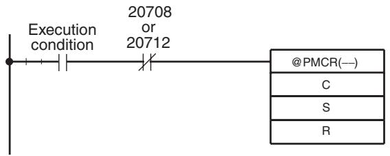
flowchart
graph LR
A["Execution condition"] --> B["20708 or 20712"]
B --> C["@PMCR(---)"]
C --> D["C"]
C --> E["S"]
C --> F["R"]
Control Word (C)
The first digit of the control word (1 or 2) specifies the Serial Communications Board port and the last three digits specify the communications sequence (000 to 999), as shown in the following diagram.
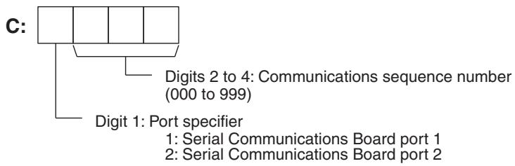
First Send Word (S)
The first word of the words required to send data is specified. S contains the number of words to be sent +1 (i.e., including the S word) and send data starts in S+1. Between 0 and 0128 words can be sent.
If there is no send data, always set 0000 as a constant for S. An error will occur and the Error Flag will turn ON if any other constant or a word address is given and PMCR(—) will not be executed.
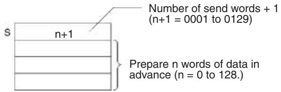
First Receive Word (R)
These words contain received data. Specify a word address for R even if no data is being received. If a constant is set for R, an error will occur, the Error Flag will turn ON, and PMCR(—) will not be executed.
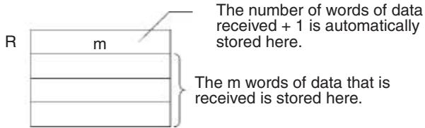
Flags
ER: Indirectly addressed EM/DM word is non-existent.
(Content of *EM/*DM word is not BCD, or the EM/DM area boundary has been exceeded.)
R is not BCD or DM 6144 through DM 6655 has been used for R.
Another PMCR(—) instruction was already in progress and the Protocol Macro Executing Flag was ON when the instruction was executed.
The port specifier was not 1 or 2.
Example
PMCR(—) executes communications sequence 101 when IR 00000 is ON and SR 20708 (the Port 1 Protocol Macro Executing Flag) is OFF. DM 0100 contains 0003, so the next two words (DM 0101 and DM 0102) are used as the send data.
Received data is stored in the range of words beginning at DM 0201 and the number of words received is automatically written to DM 0200 (the first receive word.)
Note The symbol read option, R(), in the send message, or the symbol write option, W(), actually sends/receives data.
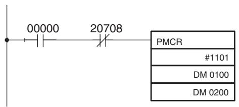
| Address | Instruction | Operands |
| 00200 | LD | 00000 |
| 00201 | AND NOT | 20708 |
| 00202 | PMCR(--) | |
| # 1101 | ||
| DM 0100 | ||
| DM 0200 |
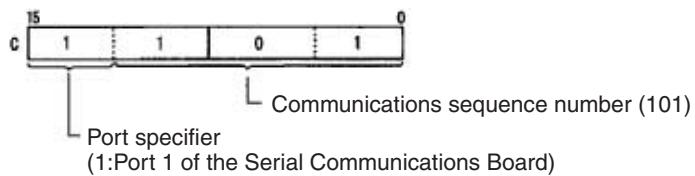
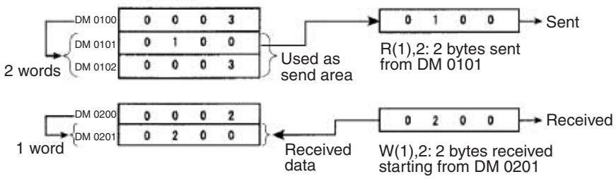
flowchart
graph TD
A["2 words"] --> B["DM 0100: 0 0 0 3"]
A --> C["DM 0101: 0 1 0 0"]
A --> D["DM 0102: 0 0 0 3"]
B --> E["Used as send area"]
C --> E
D --> E
E --> F["R(1),2: 2 bytes sent from DM 0101"]
G["1 word"] --> H["DM 0200: 0 0 0 2"]
G --> I["DM 0201: 0 2 0 0"]
H --> J["Received data"]
I --> J
J --> K["W(1),2: 2 bytes received starting from DM 0201"]
L["Sent"] --> M["Output"]
5-31 Advanced I/O Instructions
5-31-1 7-SEGMENT DISPLAY OUTPUT - 7SEG(88)
Ladder Symbols
Operand Data Areas
| S: First source word |
| IR, SR, AR, DM, EM, HR, TIM/CNT, LR |
O: Output word
| IR, SR, AR, HR, LR,TIM/CNT, DM, EM |
C: Control data
| 000 to 007 |
Limitations
Do not use 7SEG(88) more than twice in the program.
Description
When the execution condition is OFF, 7SEG(88) is not executed. When the execution condition is ON, 7SEG(88) reads the source data (either 4 or 8-digit), converts it to 7-segment display data, and outputs that data to the 7-segment display connected to the output indicated by O.
The value of C indicates the number of digits of source data and the logic for the Input and Output Units, as shown in the following table.
| Source data | Display's data input logic | Display's latch input logic | C |
| 4 digits (S) | Same as Output Unit | Same as Output Unit | 0000 |
| Different from Output Unit | 0001 | ||
| Different from Output Unit | Same as Output Unit | 0002 | |
| Different from Output Unit | 0003 | ||
| 8 digits (S, S+1) | Same as Output Unit | Same as Output Unit | 0004 |
| Different from Output Unit | 0005 | ||
| Different from Output Unit | Same as Output Unit | 0006 | |
| Different from Output Unit | 0007 |
If there are 8 digits of source data, they are placed in S and S+1, with the most significant digits placed in S+1. If there are 4 digits of source data, they are placed in S.
7SEG(88) displays the 4 or 8-digit data in 12 cycles, and then starts over and continues displaying the data.
Refer to page 424 for more information on 7SEG(88) and its applications.
Flags
ER: S and S+1 are not in the same data area. (When set to display 8-digit data.)
Indirectly addressed EM/DM word is non-existent.
(Content of *EM/*DM word is not BCD, or the EM/DM area boundary has been exceeded.)
There is an error in operand settings.
SR 25409: ON while 7SEG(88) is being executed.
Hardware
The 7-segment display is connected to an Output Unit as shown in the diagram below. For 4-digit display, the data outputs (D0 to D3) are connected to output points 0 through 3, and latch outputs (CS0 to CS3) are connected to output points 4 through 7. Output point 12 (for 8-digit display) or output point 8 (for 4-digit display) will be turned ON when one round of data is displayed, but there is no need to connect them unless required by the application.

flowchart
graph TD
subgraph_Left_Flop_1["LE0"]
D0["D0"] --> LE3["LE3"]
D1["D1"] --> LE2["LE2"]
D2["D2"] --> LE1["LE1"]
D3["D3"] --> LE0["LE0"]
end
subgraph_Left_Flop_2["LE1"]
VDD["V_DD (+)"] --> LE0
VSS["V_SS (0)"] --> LE0
VDD --> LE3
VSS --> LE3
VDD --> LE2
VSS --> LE2
VDD --> LE1
VSS --> LE1
VDD --> LE0
end
subgraph_Left_Flop_3["LE2"]
D0["D0"] --> LE0
D1["D1"] --> LE0
D2["D2"] --> LE0
D3["D3"] --> LE0
end
Left_Flop_4["LE3"]
Left_Flop_5["LE2"]
Left_Flop_6["LE1"]
Left_Flop_7["LE0"]
Left_Flop_8["LE1"]
Left_Flop_9["LE2"]
Left_Flop_10["LE1"]
Left_Flop_11["LE2"]
Left_Flop_12["LE1"]
Left_Flop_13["LE2"]
Left_Flop_14["LE1"]
Left_Flop_15["LE2"]
Left_Flop_16["LE1"]
Left_Flop_17["LE2"]
Left_Flop_18["LE1"]
Left_Flop_19["LE2"]
Left_Flop_20["LE0"]
Left_Flop_21["LE3"]
Left_Flop_22["LE2"]
Left_Flop_23["LE1"]
Left_Flop_24["LE0"]
Left_Flop_25["LE3"]
Left_Flop_26["LE2"]
Left_Flop_27["LE1"]
Left_Flop_28["LE0"]
Left_Flop_29["LE3"]
Left_Flop_30["LE2"]
Left_Flop_31["LE1"]
Left_Flop_32["LE0"]
Left_Flop_33["LE3"]
Left_Flop_34["LE2"]
Left_Flop_35["LE1"]
Left_Flop_36["LE0"]
Left_Flop_37["LE3"]
Left_Flop_38["LE2"]
Left_Flop_39["LE1"]
Left_Flop_40["LE0"]
Left_Flop_41["LE3"]
Left_Flop_42["LE2"]
Left_Flop_43["LE1"]
Left_Flop_44["LE0"]
Left_Flop_45["LE3"]
Left_Flop_46["LE2"]
Left_Flop_47["LE1"]
Left_Flop_48["LE0"]
Left_Flop_49["LE3"]
Left_Flop_50["LE2"]
Left_Flop_51["LE1"]
Left_Flop_52["LE0"]
Left_Flop_53["LE3"]
Left_Flop_54["LE2"]
Left_Flop_55["LE1"]
Left_Flop_56["LE0"]
Left_Flop_57["LE3"]
Left_Flop_58["LE2"]
Left_Flop_59["LE1"]
Left_Flop_60["LE0"]
Left_Flop_61["LE3"]
Left_Flop_62["LE2"]
Left_Flop_63["LE1"]
Left_Flop_64["LE0"]
Left_Flop_65["LE3"]
Left_Flop_66["LE2"]
Left_Flop_67["LE1"]
Left_Flop_68["LE0"]
Left_Flop_69["LE3"]
Left_Flop_70["LE2"]
Left_Flop_71["LE1"]
Left_Flop_72["LE0"]
Left_Flop_73["LE3"]
Left_Flop_74["LE2"]
Left_Flop_75["LE1"]
Left_Flop_76["LE0"]
Left_Flop_77["LE3"]
Left_Flop_78["LE2"]
Left_Flop_79["LE1"]
Left_Flop_80["LE0"]
left of Right_Down_OOD212
right_of_Down_OOD212
right_of_Down_OOD212
right_of_Down_OOD212
right_of_Down_OOD212
right_of_Down_OOD212
right_of_Down_OOD212
right_of_Down_OOD212
right_of_Down_OOD212
right_of_Down_OOD212
right_of_COM
The outputs can be connected from a Transistor Output Unit with 8 or more output points for four digits or 16 or more output points for eight digits.
Note
- Output Unit outputs normally employ negative logic. (Only the PNP output type employs positive logic.)
- The 7-segment display may require either positive or negative logic, depending on the model.
Using the Instruction
S: First source word
O: Output word
C: Control data
If the first word holding the data to be displayed is specified at S, and the output word is specified at O, and the SV taken from the table below is specified at C, then operation will proceed as shown below when the program is executed.
Data Storage Format
Leftmost 4 digits
Rightmost 4 digits
S+1
S
If only four digits are displayed, then only word S will be used.
Set Values for Selecting Logic and Number of Digits (C)
| Number of digits displayed | Display Unit data input and Output Unit logic | Display Unit latch input and Output Unit logic | C setting data |
| 4 digits (4 digits, 1 block) | Same | Same | 000 |
| Different | 001 | ||
| Different | Same | 002 | |
| Different | 003 | ||
| 8 digits (4 digits, 2 blocks) | Same | Same | 004 |
| Different | 005 | ||
| Different | Same | 006 | |
| Different | 007 |
Note Do not set C to values other than 000 to 007.
| Function | Bit(s) in O | Output status (Data and latch logic depends on C) | |
| (4 digits, 1 block) | (4 digits, 2 blocks) | ||
| Data output | 00 to 03 | 00 to 0304 to 07 | Note 0 to 3: Data output for word S4 to 7: Data output for word S+1 |
| Latch output 0 | 04 | 08 | 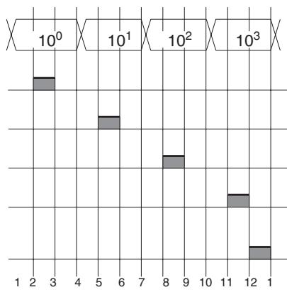 |
| Latch output 1 | 05 | 09 | |
| Latch output 2 | 06 | 10 | |
| Latch output 3 | 07 | 11 | |
| One Round Flag | 08 | 12 | 12 cycles required to complete one round |
SR 25409 will turn ON while 7SEG(88) is being executed.
Note
- Do not use 7SEG(88) more than once within the same program.
- Consider the cycle time and the characteristics of the 7-segment display when designing the system.
- Output bits not used here can be used as ordinary output bits.
With this instruction, 4 digits or 8 digits are displayed in 12 cycles.
Operation will proceed from the first execution without regard to the status prior to execution.
Application Example
This example shows a program for displaying the CQM1's 8-digit BCD numbers at the 7-segment LED display. Assume that the 7-segment display is connected to output word IR 100. Also assume that the Output Unit is using negative logic, and that the 7-segment display logic is also negative for data signals and latch signals.
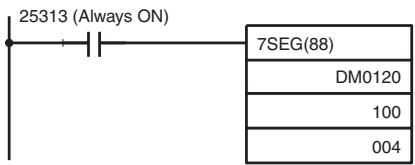
The 8-digit BCD data in DM 0120 (rightmost 4 digits) and DM 0121 (leftmost 4 digits) are always displayed by means of 7SEG(88). When the contents of DM 0120 and DM 0121 change, the display will also change.
5-31-2 DIGITAL SWITCH INPUT - DSW(87)
Ladder Symbols
| DSW(87) |
| IW |
| OW |
| R |
Operand Data Areas
| IW: Input word |
| IR, SR, AR, DM, EM, HR, TIM/CNT, LR |
| OW: Output word |
| IR, SR, AR, DM, EM, HR, TIM/CNT, LR |
| R: First result word |
| IR, SR, AR, DM, EM, HR, TIM/CNT, LR |
Limitations
DM 6144 to DM 6655 cannot be used for R.
Description
DSW(87) is used to read the value set on a digital switch connected to I/O Units. When the execution condition is OFF, DSW(87) is not executed. When the execution condition is ON, DSW(87) reads the value (either 4 or 8-digit) set on the digital switch from IW and places the result in R.
If the value is an 8-digit number, it is placed in R and R+1, with the most significant digits placed in R+1. The number of digits is set in DM 6639 of the PC Setup.
DSW(87) reads the 4 or 8-digit data in 12 cycles, and then starts over and continues reading the data.
Refer to page 427 for more information on DSW(87) and its applications.
Flags
ER: IW and/or OW are not allocated to the correct I/O Units.
Indirectly addressed EM/DM word is non-existent.
(Content of *EM/*DM word is not BCD, or the EM/DM area boundary has been exceeded.)
R and R+1 are not in the same data area. (When the CQM1H is set to receive 8-digit data.)
SR 25410: ON while DSW(87) is being executed.
Hardware
Connect the digital switch and the Input and Output Units as shown in the diagram below. In the diagram, an 8-digit input is shown. When using a 4-digit input, connect D0 through D3 from the digital switch to input points 0 through 3. In either case, output point 5 will be turned ON when one round of data is read, but there is no need to connect output point 5 unless required for the application.
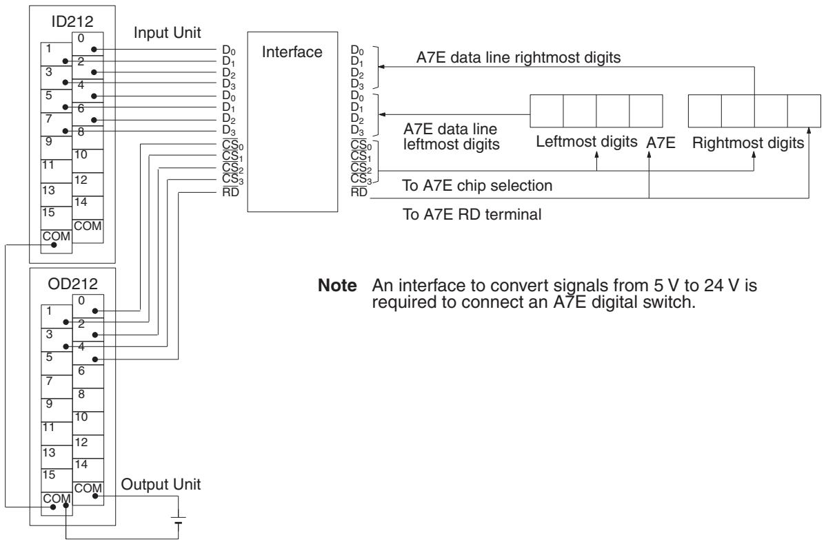
flowchart
graph TD
subgraph_ID212["ID212"]
A0["0"] --> B0["D0"]
A1["2"] --> B1["D1"]
A2["4"] --> B2["D2"]
A3["6"] --> B3["D3"]
A4["8"] --> B4["D4"]
A5["10"] --> B5["D5"]
A6["12"] --> B6["D6"]
A7["14"] --> B7["D7"]
A8["COM"] --> B8["CS0"]
A9["COM"] --> B9["CS1"]
A10["COM"] --> B10["CS2"]
A11["COM"] --> B11["CS3"]
A12["COM"] --> B12["CS4"]
A13["COM"] --> B13["CS5"]
A14["COM"] --> B14["CS6"]
A15["COM"] --> B15["CS7"]
A16["COM"] --> B16["CS8"]
A17["COM"] --> B17["CS9"]
A18["COM"] --> B18["CS10"]
A19["COM"] --> B19["CS11"]
A20["COM"] --> B20["CS12"]
A21["COM"] --> B21["CS13"]
A22["COM"] --> B22["CS14"]
A23["COM"] --> B23["CS15"]
A24["COM"] --> B24["CS16"]
A25["COM"] --> B25["CS17"]
A26["COM"] --> B26["CS18"]
A27["COM"] --> B27["CS19"]
A28["COM"] --> B28["CS20"]
A29["COM"] --> B29["CS21"]
A30["COM"] --> B30["CS22"]
A31["COM"] --> B31["CS23"]
A32["COM"] --> B32["CS24"]
A33["COM"] --> B33["CS25"]
A34["COM"] --> B34["CS26"]
A35["COM"] --> B35["CS27"]
A36["COM"] --> B36["CS28"]
A37["COM"] --> B37["CS29"]
A38["COM"] --> B38["CS30"]
A39["COM"] --> B39["CS31"]
A40["COM"] --> B40["CS32"]
A41["COM"] --> B41["CS33"]
A42["COM"] --> B42["CS34"]
A43["COM"] --> B43["CS35"]
A44["COM"] --> B44["CS36"]
A45["COM"] --> B45["CS37"]
A46["COM"] --> B46["CS38"]
A47["COM"] --> B47["CS39"]
A48["COM"] --> B48["CS40"]
A49["COM"] --> B49["CS41"]
A50["COM"] --> B50["CS42"]
A51["COM"] --> B51["CS43"]
A52["COM"] --> B52["CS44"]
A53["COM"] --> B53["CS45"]
A54["COM"] --> B54["CS46"]
A55["COM"] --> B55["CS47"]
A56["COM"] --> B56["CS48"]
A57["COM"] --> B57["CS49"]
A58["COM"] --> B58["CS50"]
A59["COM"] --> B59["CS51"]
A60["COM"] --> B60["CS52"]
A61["COM"] --> B61["CS53"]
A62["COM"] --> B62["CS54"]
A63["COM"] --> B63["CS55"]
A64["COM"] --> B64["CS56"]
A65["COM"] --> B65["CS57"]
A66["COM"] --> B66["CS58"]
A67["COM"] --> B67["CS59"]
A68["COM"] --> B68["CS60"]
A69["COM"] --> B69["CS61"]
A70["COM"] --> B70["CS62"]
A71["COM"] --> B71a["D0-D0 leftmost digits"]
A72["D0-D0 leftmost digits rightmost digits to A7E chip selection to A7E RD terminal"]
end
subgraph OutputUnit
O0
end
Note["Note An interface to convert signals from 5 V to 24 V is required to connect an A7E digital switch."]
The following example illustrates connections for an A7B Thumbwheel Switch.
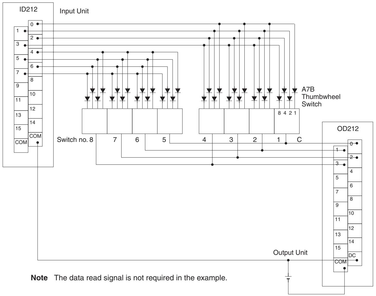
flowchart
graph TD
subgraph_ID212["ID212"]
A0["0"] --> B1["Switch no. 8"]
A2["2"] --> B1
A3["4"] --> B1
A5["6"] --> B1
A7["8"] --> B1
A9["10"] --> B1
A11["12"] --> B1
A13["14"] --> B1
A15["COM"] --> B1
end
subgraph_ODA212["OD212"]
C0["0"] --> D0["Output Unit"]
C1["2"] --> D0
C3["4"] --> D0
C5["6"] --> D0
C7["8"] --> D0
C9["10"] --> D0
C11["12"] --> D0
C13["14"] --> D0
C15["DC"] --> D0
end
B1 -->|Arrow down| B2
B2 -->|Arrow down| B3
B3 -->|Arrow down| B4
B4 -->|Arrow down| B5
B5 -->|Arrow down| B6
B6 -->|Arrow down| B7
B7 -->|Arrow down| B8
B8 -->|Arrow down| B9
B9 -->|Arrow down| B10
B10 -->|Arrow down| B11
B11 -->|Arrow down| B12
B12 -->|Arrow down| B13
B13 -->|Arrow down| B14
B14 -->|Arrow down| B15
B15 -->|Arrow down| B16
B16 -->|Arrow down| B17
B17 -->|Arrow down| B18
B18 -->|Arrow down| B19
B19 -->|Arrow down| B20
B20 -->|Arrow down| B21
B21 -->|Arrow down| B22
B22 -->|Arrow down| B23
B23 -->|Arrow down| B24
B24 -->|Arrow down| B25
B25 -->|Arrow down| B26
B26 -->|Arrow down| B27
B27 -->|Arrow down| B28
B28 -->|Arrow down| B29
B29 -->|Arrow down| B30
B30 -->|Arrow down| B31
B31 -->|Arrow down| B32
B32 -->|Arrow down| B33
B33 -->|Arrow down| B34
B34 -->|Arrow down| B35
B35 -->|Arrow down| B36
B36 -->|Arrow down| B37
B37 -->|Arrow down| B38
B38 -->|Arrow down| B39
B39 -->|Arrow down| B40
B40 -->|Arrow down| B41
B41 -->|Arrow down| B42
B42 -->|Arrow down| B43
B43 -->|Arrow down| B44
B44 -->|Arrow down| B45
B45 -->|Arrow down| B46
B46 -->|Arrow down| B47
B47 -->|Arrow down| B48
B48 -->|Arrow down| B49
B49 -->|Arrow down| B50
B50 -->|Arrow down| OutputUnit["Output Unit"]
note["Note: The data read signal is not required in the example."]
The inputs can be connected to the CPU Unit's input terminals or a DC Input Unit with 8 or more input points and the outputs can be connected from a Transistor Output Unit with 8 or more output points.
Preparations
When using DSW(87), make the following setting in the PC Setup in PROGRAM mode before executing the program.
Digital Switch Settings (PC Setup)
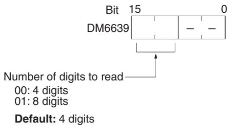
Do not make any changes to bits 0 to 7. They are not related to DSW(87).
Using the Instruction
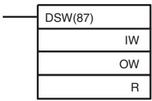
IW: Input word
OW: Output word
R: First register word
If the input word for connecting the digital switch is specified at for IW, and the output word is specified for OW, then operation will proceed as shown below when the program is executed.
16 cycles to complete one round of execution
SR 25410 will turn ON while DSW(87) is being executed.
Note
- Do not use DSW(87) more than once within the same program.
- When using DSW(87), set the input constant for the relevant input word to less than the cycle time. (Input constants can be changed from DM 6620 onwards.) The characteristics of the digital switch must also be considered in system and program design.
- Input and output bits not used here can be used as ordinary input and output bits.
With this instruction, 4-digit or 8-digit set values can be read in 16 cycles.
Application Example
This example shows a program for reading 4 digits in BCD from the digital switch. Assume that the digital switch is connected to IR 000 (input) and IR 100 (output), and assume the default status for all the PC Setup (4 digits to read).
The data set from the digital switch by DSW(87) is stored in HR 51.
When IR 00015 turns ON, the value stored in HR 51 is moved to DM 0001.
flowchart
graph TD
A["25313"] --> B["DSW(87)"]
A --> C["000"]
A --> D["100"]
A --> E["HR51"]
F["00015"] --> G["@MOV(21)"]
G --> H["HR51"]
G --> I["DM0000"]
Note Output point 5 (here, IR 10005) turns on when one round of data is read and can be used to time switching the data storage area and gate signal (CS signal) when DSW(87) is used to input data to different areas of memory.
5-31-3 HEXADECIMAL KEY INPUT - HKY(—)
Ladder Symbols
| HKY(—) |
| IW |
| OW |
| D |
Operand Data Areas
| IW: Input word |
| IR, SR, AR, DM, EM, HR, TIM/CNT, LR |
| OW: Control signal output word |
| IR, SR, AR, DM, EM, HR, TIM/CNT, LR |
| D: First register word |
| IR, SR, AR, DM, EM, HR, TIM/CNT, LR |
Limitations
D and D+2 must be in the same data area.
Do not use HKY(—) more than twice in the program.
DM 6144 to DM 6655 cannot be used for D.
Description
When the execution condition is OFF, HKY(—) is not executed. When the execution condition is ON, HKY(—) inputs data from a hexadecimal keypad connected to the input indicated by IW. The data is input in two ways:
1,2,3...
- An 8-digit shift register is created in D and D+1. When a key is pressed on the hexadecimal keypad, the corresponding hexadecimal digit is shifted into the least significant digit of D. The other digits of D, D+1 are shifted left and the most significant digit of D+1 is lost.
- The bits of D+2 and bit 4 of OW indicate key input. When one of the keys on the keypad (0 to F) is being pressed, the corresponding bit in D+2 (00 to 15) and bit 4 of OW are turned ON.
Note When one of the keypad keys is being pressed, input from the other keys is disabled.
HKY(—) inputs each digit in 3 to 12 cycles, and then starts over and continues inputting. Refer to page 431 for more details on HKY(—).
Flags
ER: Indirectly addressed EM/DM word is non-existent.
(Content of *EM/*DM word is not BCD, or the EM/DM area boundary has been exceeded.)
D and D+2 are not in the same data area.
SR 25408: ON while HKY(—) is being executed.
Hardware
Prepare the hexadecimal keyboard, and connect the 0 to F numeric key switches, as shown below, to input points 0 through 3 and output points 0 through 3. Output point 4 will be turned ON while any key is being pressed, but there is no need to connect it.
flowchart
graph TD
A["ID212"] -->|0| B["Output Unit"]
A -->|1| C["OD212"]
A -->|2| C
A -->|3| C
A -->|4| C
A -->|5| C
A -->|6| C
A -->|7| C
A -->|8| C
A -->|9| C
A -->|10| C
A -->|11| C
A -->|12| C
A -->|13| C
A -->|14| C
A -->|15| C
A -->|COM| C
B --> D["0"]
B --> E["1"]
B --> F["2"]
B --> G["3"]
B --> H["4"]
B --> I["5"]
B --> J["6"]
B --> K["7"]
B --> L["8"]
B --> M["9"]
B --> N["10"]
B --> O["11"]
B --> P["12"]
B --> Q["13"]
B --> R["14"]
B --> S["COM"]
B --> T["Output Unit"]
Input Unit
The inputs can be connected to the input terminals on the CPU Unit or a DC Input Unit with 8 or more input points and the outputs can be connected from a Transistor Output Unit with 8 points or more.
Using the Instruction
IW: Input word
OW: Control signal output word
D: First register word
If the input word for connecting the hexadecimal keyboard is specified at IW, and the output word is specified at OW, then operation will proceed as shown below when the program is executed.
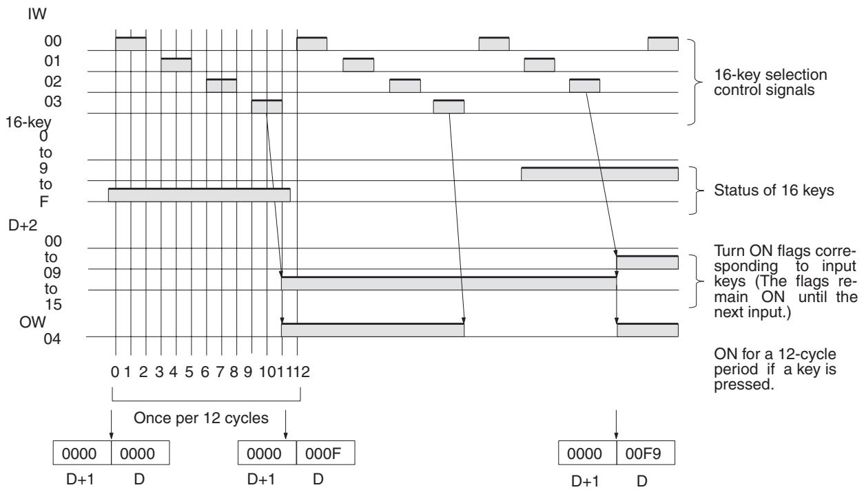
other
| Signal | Value | |--------|-------| | 00 | 0000 | | 01 | 0000 | | 02 | 0000 | | 03 | 0000 | | 16-key | 0000 | | to | 0000 | | 9 | 0000 | | to | 0000 | | F | 0000 | | D+2 | 0000 | | 00 | D+1 | | to | D+1 | | 09 | D+1 | | to | D+1 | | 15 | D+1 | | OW | D+1 | | 04 | D+1 | | | D | | | D | | | D | | | D | | | D | | | D | | | D | | | D | | | D | | | D | | | D | | | D | | | D | | | D | | | D | | | D | | | D | | 16-key | selection control signals | | Status | 16 keys | | Turn ON flags corresponding to input keys (The flags remain ON until the next input.) | 16 keys | | ON for a 12-cycle period if a key is pressed. | On for a 12-cycle period if a key is pressed.SR 25408 will turn ON while HKY(—) is being executed.
Note
- Do not use HKY(—) more than once within the same program.
- When using HKY(—), set the input constant for the relevant input word to less than the cycle time. (Input constants can be changed from DM 6620 onwards.)
- While one key is being pressed, input from other keys will not be accepted.
- If more than eight digits are input, digits will be deleted beginning with the leftmost digit.
- Input and output bits not used here can be used as ordinary input and output bits.
With this instruction, one key input is read in 3 to 12 cycles. More than one cycle is required because the ON keys can only be determined as the outputs are turned ON to test them.
Application Example
This example shows a program for inputting numbers from a hexadecimal keyboard. Assume that the hexadecimal keyboard is connected to IR 000 (input) and IR 100 (output).
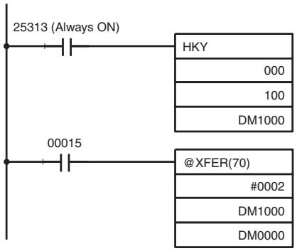
The hexadecimal key information that is input to IR 000 by HKY(—) is converted to hexadecimal and stored in words DM1000 and DM1001.
IR 00015 is used as an “ENTER key,” and when IR 00015 turns ON, the numbers stored in DM 1000 and DM 1001 are transferred to DM 0000 and DM 0001.
5-31-4 TEN KEY INPUT – TKY(18)
Ladder Symbols
| TKY(18) |
| IW |
| D1 |
| D2 |
Operand Data Areas
| IW: Input word |
| IR, SR, AR, DM, EM, HR, TIM/CNT, LR |
| D1: First register word |
| IR, SR, AR, DM, EM, HR, TIM/CNT, LR |
| D2: Key input word |
| IR, SR, AR, DM, EM, HR, TIM/CNT, LR |
Limitations
D_1 and D_1+1 must be in the same data area.
DM 6143 to DM 6655 cannot be used for D_1 .
Description
When the execution condition is OFF, TKY(18) is not executed. When the execution condition is ON, TKY(18) inputs data from a ten-key keypad connected to the input indicated by IW. The data is input in two ways:
1,2,3...
- An 8-digit shift register is created in D_1 and D_1+1 . When a key is pressed on the ten-key keypad, the corresponding BCD digit is shifted into the least significant digit of D_1 . The other digits of D_1 , D_1+1 are shifted left and the most significant digit of D_1+1 is lost.
- The first ten bits of D_2 indicate key input. When one of the keys on the keypad (0 to 9) is being pressed, the corresponding bit of D_2 (00 to 09) is turned ON.
Note When one of the keypad keys is being pressed, input from the other keys is disabled.
TKY(18) can be used in several locations in the program by changing the input word, IW. Refer to page 434 for more details on TKY(18).
Flags
ER: Indirectly addressed EM/DM word is non-existent.
(Content of *EM/*DM word is not BCD, or the EM/DM area boundary has been exceeded.)
D_1 and D_1+1 are not in the same data area.
Hardware
Prepare a 10-key keypad, and connect it so that the switches for numeric keys 0 through 9 are input to points 0 through 9 as shown in the following diagram. Either the input terminals on the CPU Unit or the inputs on a DC Input Unit with 16 or more input points can be used.
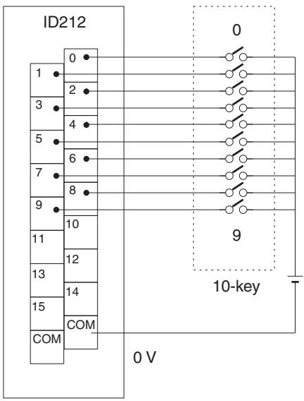
DC Input Unit
Using the Instruction
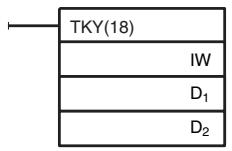
IW: Input word
D1: First register word
D_2 : Key input word
If the input word for connecting the 10-key keypad is specified for IW, then operation will proceed as shown below when the program is executed.
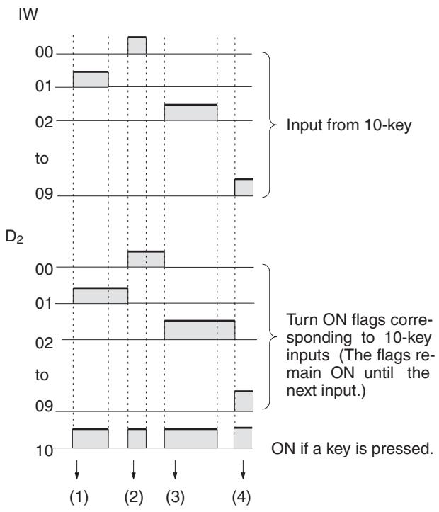
bar
| Time | IW - Input from 10-key | IW - Turn ON flags corresponding to 10-key inputs (The flags remain ON until the next input.) | D2 - Input from 10-key | D2 - Turn ON flags corresponding to 10-key inputs (The flags remain ON until the next input.) | D2 - ON if a key is pressed | |------|------------------------|----------------------------------------------------------------------------------|------------------------|----------------------------------------------------------------------------------|----------------------------| | 00 | 0.0 | 0.0 | 0.0 | 0.0 | 0.0 | | 01 | 0.1 | 0.1 | 0.1 | 0.1 | 0.1 | | 02 | 0.2 | 0.2 | 0.2 | 0.2 | 0.2 | | 09 | 0.3 | 0.3 | 0.3 | 0.3 | 0.3 | | 1 | 0.4 | 0.4 | 0.4 | 0.4 | 0.4 | | 2 | 0.5 | 0.5 | 0.5 | 0.5 | 0.5 | | 3 | 0.6 | 0.6 | 0.6 | 0.6 | 0.6 | | 4 | 0.7 | 0.7 | 0.7 | 0.7 | 0.7 |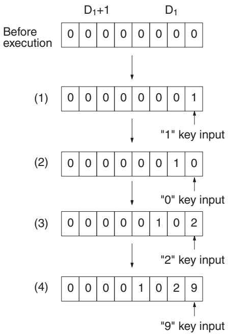
flowchart
graph TD
A["Before execution"] --> B["(1) D1+1 0 0 0 0 0 0 0 0 0"]
B --> C[""1" key input"]
C --> D["(2) D1+1 0 0 0 0 0 0 0 1 0"]
D --> E[""0" key input"]
E --> F["(3) D1+1 0 0 0 0 0 1 0 2"]
F --> G[""2" key input"]
G --> H["(4) D1+1 0 0 0 0 1 0 2 9"]
H --> I[""9" key input"]
Note 1. While one key is being pressed, input from other keys will not be accepted.
Application Example
- If more than eight digits are input, digits will be deleted beginning with the leftmost digit.
- Input bits not used here can be used as ordinary input bits.
In this example, a program for inputting numbers from the 10-key is shown. Assume that the 10-key is connected to IR 000.
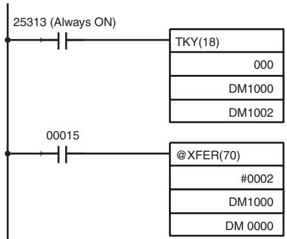
The 10-key information input to IR 000 using TKY(18) is converted to BCD and stored in DM 1000 and DM 1001. Key information is stored in DM 1002.
IR 00015 is used as an “ENTER key,” and when IR 00015 turns ON, the data stored in DM 1000 and DM 1001 will be transferred to DM 0000 and DM 0001.
SECTION 6
Host Link Commands
This section explains the methods and procedures for using Host Link commands, which can be used for Host Link communications via the CQM1H ports.
6-1 Host Link Command Summary 438
6-2 End Codes 439
6-2-1 Codes 439
6-2-2 Codes and Applicable Commands 441
6-3 Communications Procedure 442
6-4 Command and Response Formats.... 443
6-4-1 Commands from the Host Computer 443
6-4-2 Commands from the PC 446
6-5 Host Link Commands 447
6-5-1 IR/SR AREA READ — RR.... 447
6-5-2 LR AREA READ — RL 447
6-5-3 HR AREA READ — RH 448
6-5-4 PV READ — RC 448
6-5-5 TC STATUS READ — RG 449
6-5-6 DM AREA READ — RD. 449
6-5-7 EM AREA READ — RE 450
6-5-8 AR AREA READ — RJ.... 450
6-5-9 IR/SR AREA WRITE — WR 451
6-5-10 LR AREA WRITE — WL 451
6-5-11 HR AREA WRITE — WH. 452
6-5-12 PV WRITE — WC.... 452
6-5-13 TC STATUS WRITE — WG 453
6-5-14 DM AREA WRITE — WD 453
6-5-15 EM AREA WRITE — WE. 454
6-5-16 AR AREA WRITE — WJ 455
6-5-17 SV READ 1 — R# 455
6-5-18 SV READ 2 — R\$ 456
6-5-19 SV READ 3 — R% 457
6-5-20 SV CHANGE 1 — W#..... 458
6-5-21 SV CHANGE 2 — W\$...... 459
6-5-22 SV CHANGE 3 — W% 460
6-5-23 STATUS READ — MS 461
6-5-24 STATUS WRITE — SC 462
6-5-25 ERROR READ — MF 463
6-5-26 FORCED SET — KS 464
6-5-27 FORCED RESET — KR 465
6-5-28 MULTIPLE FORCED SET/RESET — FK 466
6-5-29 FORCED SET/RESET CANCEL — KC. 467
6-5-30 PC MODEL READ — MM.... 467
6-5-31 TEST—TS.... 468
6-5-32 PROGRAM READ — RP 469
6-5-33 PROGRAM WRITE — WP 469
6-5-34 COMPOUND COMMAND — QQ.... 469
6-5-35 ABORT — XZ 471
6-5-36 INITIALIZE — **...... 472
6-5-37 TXD RESPONSE — EX 472
6-5-38 Undefined Command — IC 472
6-1 Host Link Command Summary
The Host Link commands listed in the following table can be sent to the CQM1H for Host Link communications.
| Header code | PC mode | Name | Page | ||
| RUN | MON | PRG | |||
| RR | Valid | Valid | Valid | IR/SR AREA READ | 447 |
| RL | Valid | Valid | Valid | LR AREA READ | 447 |
| RH | Valid | Valid | Valid | HR AREA READ | 448 |
| RC | Valid | Valid | Valid | PV READ | 448 |
| RG | Valid | Valid | Valid | TC STATUS READ | 449 |
| RD | Valid | Valid | Valid | DM AREA READ | 449 |
| RE | Valid | Valid | Valid | EM AREA READ | 450 |
| RJ | Valid | Valid | Valid | AR AREA READ | 450 |
| WR | Not valid | Valid | Valid | IR/SR AREA WRITE | 451 |
| WL | Not valid | Valid | Valid | LR AREA WRITE | 451 |
| WH | Not valid | Valid | Valid | HR AREA WRITE | 452 |
| WC | Not valid | Valid | Valid | PV WRITE | 452 |
| WG | Not valid | Valid | Valid | TC STATUS WRITE | 453 |
| WD | Not valid | Valid | Valid | DM AREA WRITE | 453 |
| WE | Not valid | Valid | Valid | EM AREA WRITE | 454 |
| WJ | Not valid | Valid | Valid | AR AREA WRITE | 455 |
| R# | Valid | Valid | Valid | SV READ 1 | 455 |
| R | Valid | Valid | Valid | SV READ 2 | 456 |
| R% | Valid | Valid | Valid | SV READ 3 | 457 |
| W# | Not valid | Valid | Valid | SV CHANGE 1 | 458 |
| W | Not valid | Valid | Valid | SV CHANGE 2 | 459 |
| W% | Not valid | Valid | Valid | SV CHANGE 3 | 460 |
| MS | Valid | Valid | Valid | STATUS READ | 461 |
| SC | Valid | Valid | Valid | STATUS WRITE | 462 |
| MF | Valid | Valid | Valid | ERROR READ | 463 |
| KS | Not valid | Valid | Valid | FORCED SET | 464 |
| KR | Not valid | Valid | Valid | FORCED RESET | 465 |
| FK | Not valid | Valid | Valid | MULTIPLE FORCED SET/RESET | 466 |
| KC | Not valid | Valid | Valid | FORCED SET/RESET CANCEL | 467 |
| MM | Valid | Valid | Valid | PC MODEL READ | 467 |
| TS | Valid | Valid | Valid | TEST | 468 |
| RP | Valid | Valid | Valid | PROGRAM READ | 469 |
| WP | Not valid | Not valid | Valid | PROGRAM WRITE | 469 |
| Valid | Valid | Valid | COMPOUND COMMAND | 469 | |
| XZ | Valid | Valid | Valid | ABORT (command only) | 471 |
| ** | Valid | Valid | Valid | INITIALIZE (command only) | 472 |
| EX | Valid | Valid | Not valid | TXD RESPONSE (response only) | 472 |
| IC | --- | --- | --- | Undefined command (response only) | 472 |
6-2 End Codes
6-2-1 Codes
The response (end) codes listed in the following table are returned in the response frame for Host Link commands. When two or more errors occur, the end code for the first error will be returned.
| End code | Contents | Probable cause | Corrective measures |
| 00 | Normal completion | No problem exists. | --- |
| 01 | Not executable in RUN mode | The command that was sent cannot be executed when the PC is in RUN mode. | Check the relation between the command and the PC mode. |
| 02 | Not executable in MONITOR mode | The command that was sent cannot be executed when the PC is in MONITOR mode. | |
| 03 | UM write-protected | The PC's UM is write-protected. | Turn OFF pin 1 of the CPU Unit's DIP switch (SW1). |
| 04 | Address over | The program address setting in an read or write command is above the highest program address. | Check the program. |
| 13 | FCS error | The FCS is wrong. | Check the FCS calculation method. If there was influence from noise, transfer the command again. |
| 14 | Format error | The command format is wrong, or a command that cannot be divided has been divided, or the frame length is smaller than the minimum length for the applicable command. | Check the format and transfer the command again. |
| 15 | Entry number data error | The data is outside of the specified range or too long. Hexadecimal data has not been specified. | Correct the data and transfer the command again. |
| 16 | Command not supported | The operand specified in an SV Read or SV Change command does not exist in the program. | Check search data or the search starting point. |
| 18 | Frame length error | The maximum frame length of 132 bytes was exceeded. If the frame exceeds 280 bytes, the Reception Overflow Flag will be turned ON and there will not be a response. | Check the command and divide it into multiple frames if necessary. |
| 19 | Not executable | The read SV exceeded 9,999, or an I/O memory batch read was executed when items to read were not registered for composite command. | Register items to read before attempting batch read. |
| 23 | User memory protected | The UM is write-protected. | Turn OFF the write-protection |
| A3 | Aborted due to FCS error in transmission data | An FCS error occurred in the second or later frame, or there were two bytes or less of data in an intermediate or final frame for multiple writing. | Correct the command data and transfer the command again. |
| A4 | Aborted due to format error in transmission data | The command format did not match the number of bytes in the second or later frame. | |
| A5 | Aborted due to entry number data error in transmission data | There was an entry number data error in the second or later frame, a data length error, or data was not set in hexadecimal. | |
| A8 | Aborted due to frame length error in transmission data | The length of the second and later frames exceeded the maximum of 128 bytes. |
A response will not be received with some errors, regardless of the command. These errors are listed in the following table.
| Error | PC operation |
| Parity, overrun, or framing error during command reception. (Same even for commands address to other Units.) | The Communications Error Flag will be turned ON, an error code will be registered, and receptions will be reset. (The error will be cleared automatically if communications restart normally.)The Communications Error Flags are as follows:Peripheral port: AR 0812Built-in RS-232C port: AR 0804Serial Communications Board port 1: IR 20104, Serial Communications Board port 2: IR 20112 |
| A command is received that does not have the @ character at the beginning of the first frame. | The command will be discarded. |
| Incorrect node number (Not a local unit or over 30) | The command will be discarded. |
| The data in an intermediate or final frame for multiframe writes is longer than 2 bytes. | An FCS error will occur. |
6-2-2 Codes and Applicable Commands
The following table shows which end codes can be returned for each command.
| Header | Possible End Codes | Comments | ||||||||||||
| RR | 00 | 13 | 14 | 15 | 18 | A3 | A8 | --- | ||||||
| RL | 00 | 13 | 14 | 15 | 18 | A3 | A8 | --- | ||||||
| RH | 00 | 13 | 14 | 15 | 18 | A3 | A8 | --- | ||||||
| RC | 00 | 13 | 14 | 15 | 18 | A3 | A8 | --- | ||||||
| RG | 00 | 13 | 14 | 15 | 18 | A3 | A8 | --- | ||||||
| RD | 00 | 13 | 14 | 15 | 18 | A3 | A8 | --- | ||||||
| RE | 00 | 13 | 14 | 15 | 18 | A3 | A8 | --- | ||||||
| RJ | 00 | 13 | 14 | 15 | 18 | --- | ||||||||
| WR | 00 | 01 | 13 | 14 | 15 | 18 | A3 | A4 | A5 | A8 | --- | |||
| WL | 00 | 01 | 13 | 14 | 15 | 18 | A3 | A4 | A5 | A8 | --- | |||
| WH | 00 | 01 | 13 | 14 | 15 | 18 | A3 | A4 | A5 | A8 | --- | |||
| WC | 00 | 01 | 13 | 14 | 15 | 18 | A3 | A4 | A5 | A8 | --- | |||
| WG | 00 | 01 | 13 | 14 | 15 | 18 | A3 | A4 | A5 | A8 | --- | |||
| WD | 00 | 01 | 13 | 14 | 15 | 18 | 23 | A3 | A4 | A5 | A8 | --- | ||
| WE | 00 | 01 | 13 | 14 | 15 | 18 | A3 | A4 | A5 | A8 | --- | |||
| WJ | 00 | 01 | 13 | 14 | 15 | 18 | A3 | A4 | A5 | A8 | --- | |||
| R# | 00 | 13 | 14 | 15 | 16 | 18 | 23 | --- | ||||||
| R | 00 | 04 | 13 | 14 | 15 | 16 | 18 | 23 | ||||||
| R% | 00 | 04 | 13 | 14 | 15 | 16 | 18 | 23 | ||||||
| W# | 00 | 01 | 13 | 14 | 15 | 16 | 18 | 23 | ||||||
| W | 00 | 01 | 04 | 13 | 14 | 15 | 16 | 18 | 23 | |||||
| W% | 00 | 01 | 04 | 13 | 14 | 15 | 16 | 18 | 23 | |||||
| MS | 00 | 13 | 14 | 18 | ||||||||||
| SC | 00 | 13 | 14 | 15 | 18 | 19 | ||||||||
| MF | 00 | 13 | 14 | 15 | 18 | |||||||||
| KS | 00 | 01 | 13 | 14 | 15 | 18 | ||||||||
| KR | 00 | 01 | 13 | 14 | 15 | 18 | ||||||||
| FK | 00 | 01 | 13 | 14 | 15 | 18 | ||||||||
| KC | 00 | 01 | 13 | 14 | 18 | |||||||||
| MM | 00 | 13 | 14 | 18 | ||||||||||
| TS | 13 | 14 | 18 | |||||||||||
| RP | 00 | 13 | 14 | 18 | 23 | A3 | A8 | |||||||
| WP | 00 | 01 | 02 | 13 | 14 | 15 | 18 | 19 | 23 | A3 | A4 | A5 | ||
| 00 | 13 | 14 | 15 | 18 | 19 | A3 | A4 | A5 | ||||||
| XZ | --- | |||||||||||||
| ** | --- | |||||||||||||
| IC | --- | |||||||||||||
| EX | --- | |||||||||||||
6-3 Communications Procedure
Host Link communications are executed by means of an exchange of commands and responses between the host computer and the PC.
With the CQM1H, there are two communications methods that can be used. One is the normal method, in which commands are issued from the host computer to the PC. The other method allows commands to be issued from the PC to the host computer.
Frame Transmission and Reception
Commands and responses are exchanged in the order shown in the illustration below. The block of data transferred in a single transmission is called a "frame." A single frame is configured of a maximum of 131 characters of data.
The right to send a frame is called the “transmission right.” The Unit that has the transmission right is the one that can send a frame at any given time. The transmission right is traded back and forth between the host computer and the PC each time a frame is transmitted. The transmission right is passed from the transmitting Unit to the receiving Unit when either a terminator (the code that marks the end of a command or response) or a delimiter (the code that sets frames apart) is received.
Commands from Host
In Host Link communications, the host computer ordinarily has the transmission right first and initiates the communications. The PC then automatically sends a response.
flowchart
graph TD
A["Host computer"] --> B["Frame command"]
B --> C["Unit no."]
B --> D["Header code"]
B --> E["Text"]
B --> F["FCS"]
B --> G["Terminator"]
H["PC"] --> I["Frame (response)"]
I --> J["Unit no."]
I --> K["Header code"]
I --> L["End code"]
I --> M["Text"]
I --> N["FCS"]
I --> O["Terminator"]
P["Frame (command)"] --> Q["Unit no."]
P --> R["Header code"]
P --> S["Text"]
P --> T["FCS"]
P --> U["Terminator"]
V["Frame (response)"] --> W["Unit no."]
V --> X["Header code"]
V --> Y["End code"]
V --> Z["Text"]
V --> AA["FCS"]
V --> AB["Terminator"]
Commands from PC
With CQM1H PCs, it is also possible in Host Link communications for the PC to send commands to the host computer. In this case it is the PC that has the transmission right and initiates the communications.
Host computer
PC
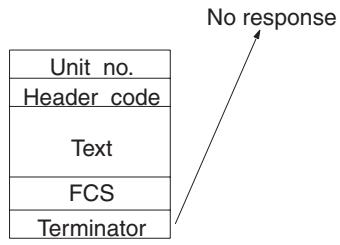
flowchart
graph TD
A["Unit no."] --> B["Header code"]
B --> C["Text"]
C --> D["FCS"]
D --> E["Terminator"]
style A fill:#f9f,stroke:#333
style B fill:#ccf,stroke:#333
style C fill:#cfc,stroke:#333
style D fill:#fcc,stroke:#333
style E fill:#ffc,stroke:#333
note right of A No response
When commands are issued to the host computer, the data is transmitted in one direction from the PC to the host computer. If a response to a command is required, use a Host Link communications command to write the response from the host computer to the PC.
6-4 Command and Response Formats
This section explains the formats for the commands and responses that are exchanged in Host Link communications.
6-4-1 Commands from the Host Computer
When a command is issued from the host computer, the command and response formats are as shown below.
Command Format
When transmitting a command from the host computer, prepare the command data in the format shown below.
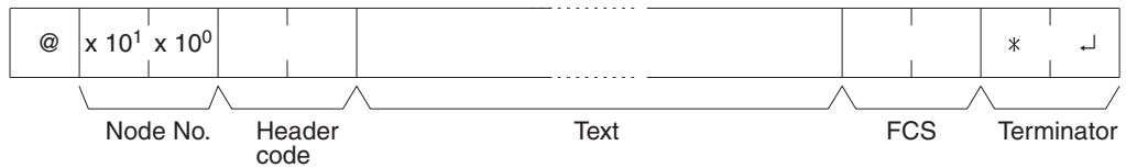
@
An “@” symbol must be placed at the beginning.
Node No.
Identifies the PC communicating with the host computer.
Specify the Host Link node number set for the PC in the PC Setup (DM 6648 and DM 6653 for CPU Unit, DM 6553 and DM 6558 for Serial Communications Board).
Header Code
Set the 2-character command code.
Text
Set the command parameters.
FCS
Set a 2-character Frame Check Sequence code. See page 445.
Terminator
Set two characters, “*” and the carriage return (CHR\$(13)) to indicate the end of the command.
Response Format
The response from the PC is returned in the format shown below. Prepare a program so that the response data can be interpreted and processed.
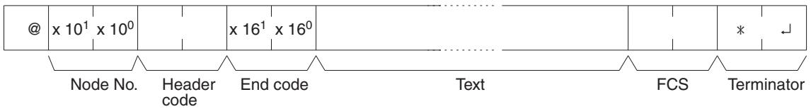
@, Node No., Header Code
Contents identical to those of the command are returned.
End Code
The completion status of the command (e.g., whether or not an error has occurred) is returned.
Text
Text is returned only when there is data such as read data.
FCS, Terminator
Refer to the corresponding explanations under “Command Format.”
Long Transmissions
The largest block of data that can be transmitted as a single frame is 131 characters. A command or response of 132 characters or more must therefore be divided into more than one frame before transmission. When a transmission is split, the ends of the first and intermediate frames are marked by a delimiter instead of a terminator.
Dividing Commands (Host Computer to PC)
As each frame is transmitted by the host computer, the computer waits for the delimiter to be transmitted from the PC. After the delimiter has been transmitted, the next frame will then be sent. This procedure is repeated until the entire command has been transmitted.
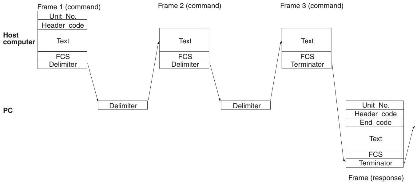
flowchart
graph TD
subgraph_Host_computer["Host computer"]
A["Unit No."] --> B["Header code"]
B --> C["Text"]
C --> D["FCS"]
D --> E["Delimiter"]
end
subgraph_PC["PC"]
F["Delimiter"] --> G["Text"]
G --> H["FCS"]
H --> I["Delimiter"]
I --> J["Text"]
J --> K["FCS"]
K --> L["Terminator"]
end
subgraph_Frame_3["Frame 3 (command)"]
M["Text"] --> N["FCS"]
N --> O["Terminator"]
end
subgraph_Frame_2["Frame 2 (command)"]
P["Text"] --> Q["FCS"]
Q --> R["Delimiter"]
R --> S["Text"]
end
subgraph_Frame_1["Frame 1 (command)"]
T["Unit No."]
U["Header code"]
V["Text"]
W["FCS"]
X["Delimiter"]
end
subgraph_Frame_response["Frame (response)"]
Y["Unit No."]
Z["Header code"]
AA["End code"]
AB["Text"]
AC["FCS"]
AD["Terminator"]
end
Dividing Responses (PC to Host Computer)
As each frame is received by the host computer, a delimiter is transmitted to the PC. After the delimiter has been transmitted, the PC will transmit the next frame. This procedure is repeated until the entire response has been transmitted.
flowchart
graph TD
A["Host computer"] --> B["Frame command"]
B --> C["Unit No."]
B --> D["Header code"]
B --> E["Text"]
B --> F["FCS"]
B --> G["Terminator"]
H["PC"] --> I["Unit No."]
H --> J["Header code"]
H --> K["End code"]
H --> L["Text"]
H --> M["FCS"]
H --> N["Terminator"]
O["Frame 2 (response)"] --> P["Delimiter"]
Q["Frame 3 (response)"] --> R["Delimiter"]
S["Text"] --> T["FCS"]
S --> U["Delimiter"]
V["Text"] --> W["FCS"]
V --> X["Terminator"]
Frame 1 (response)
Precautions for Long Transmissions
When dividing commands such as WR, WL, WC, or WD that execute write operations, be careful not to divide into separate frames data that is to be written into a single word. As shown in the illustration below, be sure to divide frames so that they coincide with the divisions between words.
Frame 1
Frame 3
FCS (Frame Check Sequence)
When a frame is transmitted, an FCS is placed just before the delimiter or terminator in order to check whether any data error has been generated. The FCS is 8-bit data converted into two ASCII characters. The 8-bit data is the result of an EXCLUSIVE OR performed on the data from the beginning of the frame until the end of the text in that frame (i.e., just before the FCS). Calculating the FCS each time a frame is received and checking the result against the FCS that is included in the frame makes it possible to check for data errors in the frame.
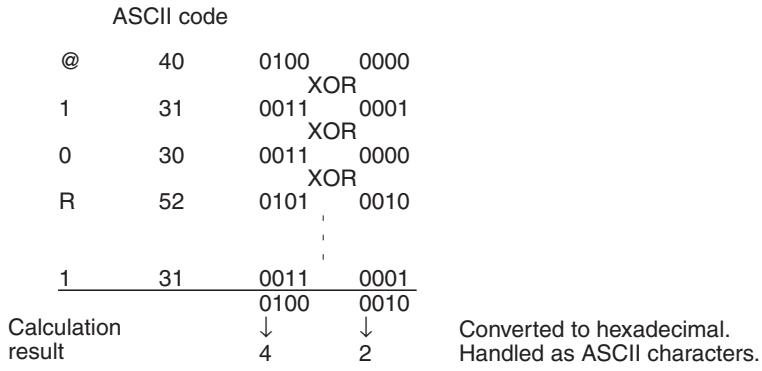
other
| ASCII code | OR | XOR | | :--- | :--- | :--- | | @ 40 | 0100 | 0000 | | 1 | 31 | 0011 | | 0 | 30 | 0011 | | R | 52 | 0101 | | 1 | 31 | 0011 | | Calculation result | ↓ | ↓ | | Calculation result | 4 | 2 | | Calculated as ASCII characters. Converted to hexadecimal. Handled as ASCII characters.Example Program for FCS
This example shows a BASIC subroutine program for executing an FCS check on a frame received by the host computer.
400 *FCSCHECK
410 L=LEN(RESPONSE$) ' ....... Data transmitted and received
420 Q=0:FCSCK$=" "
430 A=RIGHT(RESPONSE$,1)
440 PRINT RESPONSE,A,L
450 IF A="*" THEN LENGS=LEN(RESPONSE)-3
ELSE LENGS=LEN(RESPONSE$)-2
460 FCSP=MID(RESPONSE$,LENGS+1,2)' ... FCS data received
470 FOR I=1 TO LENGS' ....... Number of characters in FCS
480 Q=ASC(MID(RESPONSE,I,1)) XOR Q
490 NEXT I
500 FCSD=HEX(Q)
510 IF LEN(FCSD)=1 THEN FCSD="0"+FCSD$' ... FCS result
520 IF FCSD<>FCSP THEN FCSCCK$="ERR"
530 PRINT"FCSD=";FCSD", "FCSP=";FCSP", "FCSCCK=";FCSCCK
540 RETURN
Note
- Normal reception data includes the FCS, delimiter or terminator, and so on. When an error occurs in transmission, however the FCS or some other data may not be included. Be sure to program the system to cover this possibility.
- In this program example, the CR code (CHR\(13)) is not entered for RESPONSE\. When including the CR code, make the changes in lines 430 and 450.
6-4-2 Commands from the PC
In Host Link communications, commands are ordinarily sent from the host computer to the PC, but it is also possible for commands to be sent from the PC to the host computer. In Host Link Mode, any data can be transmitted from the PC to the host computer. To send a command to the host computer, use the TRANSMIT instruction (TXD(48)) in the PC program in Host Link Mode.
TXD(48) outputs data from the specified port (the RS-232C port, the peripheral port, or ports 1 or 2 of the Serial Communications Board). Refer to page 417 for details on using TXD(48).
Reception Format
When TXD(48) is executed, the data stored in the words beginning with the first send word is converted to ASCII and output to the host computer as a Host Link command in the format shown below. The “@” symbol, node number, header code, FCS, and delimiter are all added automatically when the transmission is sent. At the host computer, it is necessary to prepare in advance a program for interpreting and processing this format.
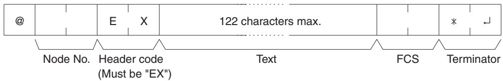
One byte of data (2 digits hexadecimal) is converted to two characters in ASCII for transmission, the amount of data in the transmission is twice the amount of words specified for TXD(48). The maximum number of characters for transmission is 122 and the maximum number of bytes that can be designated for TXD(48) is one half of that, or 61.
6-5 Host Link Commands
This section explains the commands that can be issued from the host computer to the PC.
6-5-1 IR/SR AREA READ — RR
Reads the contents of the specified number of IR and SR words, starting from the specified word.
Command Format
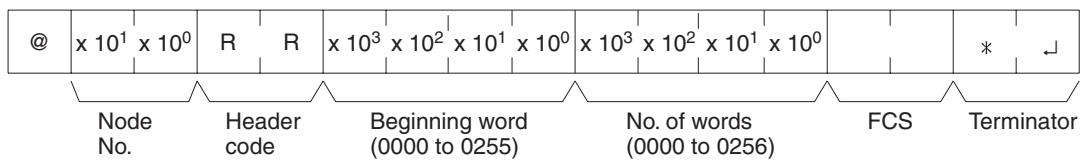
Response Format
An end code of 00 indicates normal completion.
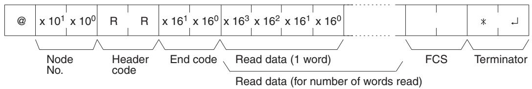
Note The response will be divided when reading more than 30 words of data.
Parameters
Read Data (Response)
The contents of the number of words specified by the command are returned in hexadecimal as a response. The words are returned in order, starting with the specified beginning word.
6-5-2 LR AREA READ — RL
Reads the contents of the specified number of LR words, starting from the specified word.
Command Format
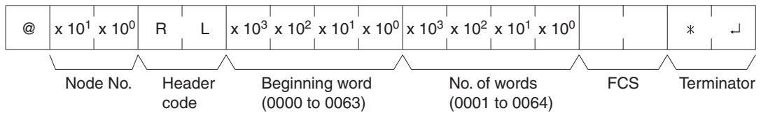
Response Format
An end code of 00 indicates normal completion.
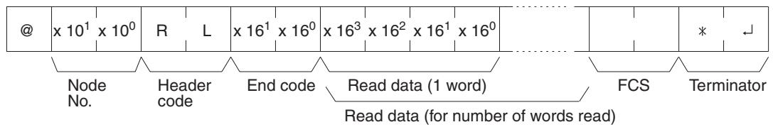
Parameters
Read Data (Response)
The contents of the number of words specified by the command are returned in hexadecimal as a response. The words are returned in order, starting with the specified beginning word.
6-5-3 HR AREA READ — RH
Reads the contents of the specified number of HR words, starting from the specified word.
Command Format
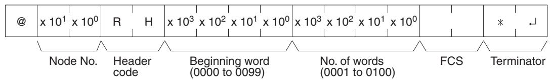
Response Format
An end code of 00 indicates normal completion.
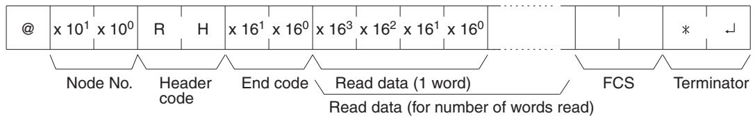
Parameters
Read Data (Response)
The contents of the number of words specified by the command are returned in hexadecimal as a response. The words are returned in order, starting with the specified beginning word.
6-5-4 PV READ — RC
Reads the contents of the specified number of timer/counter PVs (present values), starting from the specified timer/counter.
Command Format
Response Format
An end code of 00 indicates normal completion.
The response will be divided when reading more than 30 words of data.
Parameters
Read Data (Response)
The number of present values specified by the command is returned in hexadecimal as a response. The PVs are returned in order, starting with the specified beginning timer/counter.
6-5-5 TC STATUS READ — RG
Reads the status of the Completion Flags of the specified number of timers/counters, starting from the specified timer/counter.
Command Format
Response Format
An end code of 00 indicates normal completion.
The response will be divided when reading the status of more than 123 timer/counters.
Parameters
Read Data (Response)
The status of the number of Completion Flags specified by the command is returned as a response. "1" indicates that the Completion Flag is ON.
6-5-6 DM AREA READ — RD
Reads the contents of the specified number of DM words, starting from the specified word.
Command Format
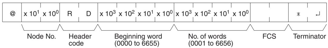
Response Format
An end code of 00 indicates normal completion.
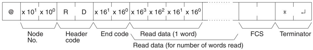
Parameters
Read Data (Response)
The contents of the number of words specified by the command are returned in hexadecimal as a response. The words are returned in order, starting with the specified beginning word.
Note Be careful about the configuration of the DM area, as it varies depending on the CPU Unit model.
6-5-7 EM AREA READ — RE
Reads the contents of the specified number of EM words, starting from the specified word in the specified EM bank.
Command Format
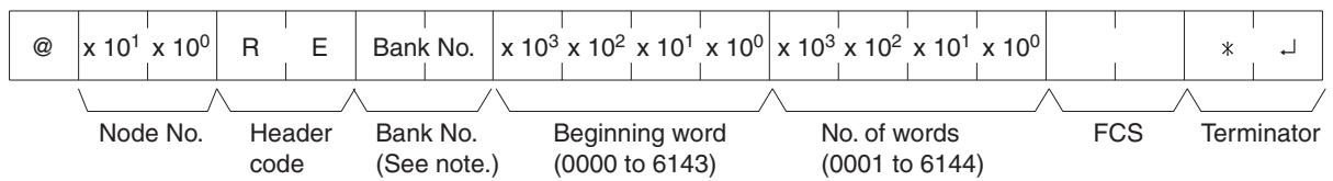
Note Input 00 Hex to specify bank number 0 or input two spaces to specify the current bank. Only the CQM1H-CPU61 CPU Unit has an EM area and it has only one bank, i.e., bank 0.
Response Format

Parameters
Read Data (Response)
The contents of the number of words specified by the command are returned in hexadecimal as a response. The words are returned in order, starting with the specified beginning word.
Note Be careful about the configuration of the EM area, as it varies depending on the CPU Unit model.
6-5-8 AR AREA READ — RJ
Reads the contents of the specified number of AR words, starting from the specified word.
Command Format
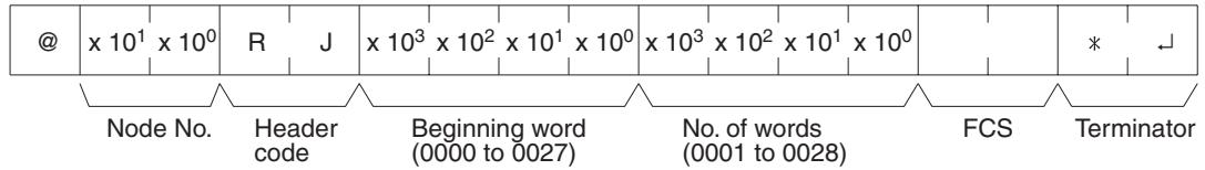
Response Format
An end code of 00 indicates normal completion.
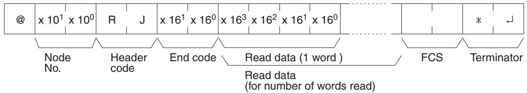
Parameters
Read Data (Response)
The contents of the number of words specified by the command are returned in hexadecimal as a response. The words are returned in order, starting with the specified beginning word.
6-5-9 IR/SR AREA WRITE — WR
Writes data to the IR and SR areas, starting from the specified word. Writing is done word by word.
Command Format
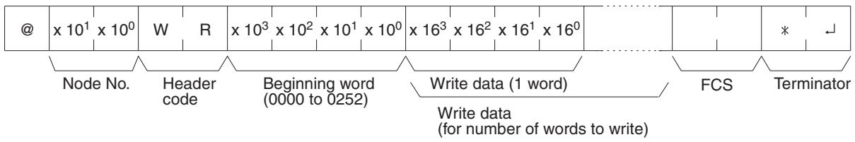
Note Divide the command when writing more than 30 words of data.
Response Format
An end code of 00 indicates normal completion.
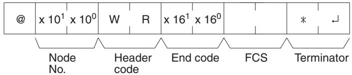
Parameter
Write Data (Command)
Specify in order the contents of the number of words to be written to the IR or SR area in hexadecimal, starting with the specified beginning word.
Note The results will be as follows depending on the first write word.
| Setting | Results |
| First write word ≤ 252 | Data will be written through word 252 but not to other words and a normal response will be returned. |
| 253 ≤ First write word ≤ 255 | No data will be written and a normal response will be returned. |
| 255 < First write word | No data will be written and an error will occur. |
6-5-10 LR AREA WRITE — WL
Writes data to the LR area, starting from the specified word. Writing is done word by word.
Command Format
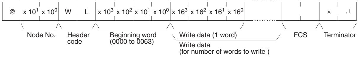
Response Format
An end code of 00 indicates normal completion.
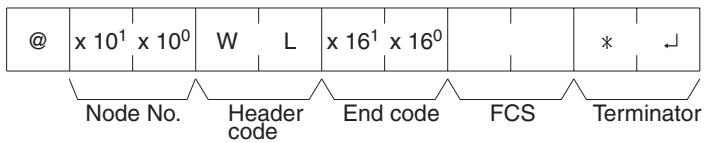
Parameters
Write Data (Command)
Specify in order the contents of the number of words to be written to the LR area in hexadecimal, starting with the specified beginning word.
Note If data is specified for writing which exceeds the allowable range, an error will be generated and the writing operation will not be executed. If, for example,
60 is specified as the beginning word for writing and five words of data are specified, then 64 will become the last word for writing data, and the command will not be executed because LR 64 is beyond area boundary.
6-5-11 HR AREA WRITE — WH
Writes data to the HR area, starting from the specified word. Writing is done word by word.
Command Format
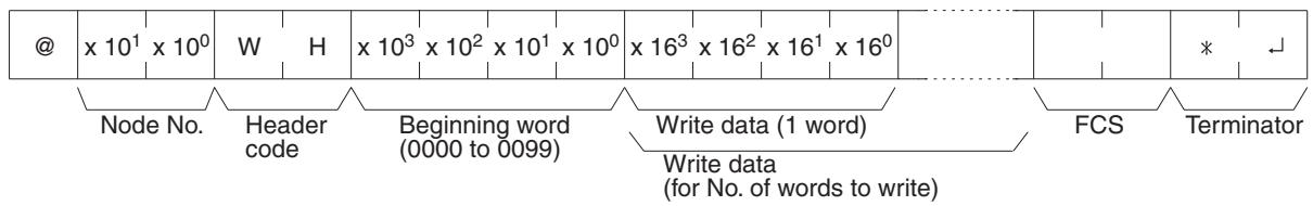
Response Format
An end code of 00 indicates normal completion.
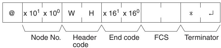
Parameter
Write Data (Command)
Specify in order the contents of the number of words to be written to the HR area in hexadecimal, starting with the specified beginning word.
Note If data is specified for writing which exceeds the allowable range, an error will be generated and the writing operation will not be executed. If, for example, 98 is specified as the beginning word for writing, and three words of data are specified, then 100 will become the last word for writing data, and the command will not be executed because HR 100 is beyond area boundary.
6-5-12 PV WRITE — WC
Writes the PVs (present values) of timers/counters starting from the specified timer/counter.
Command Format
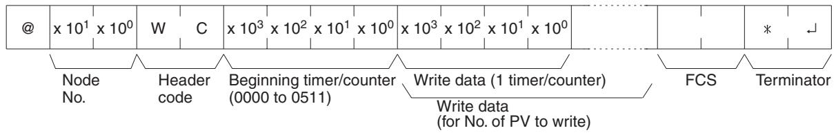
Note Divide the command when writing more than 29 words of data.
Response Format
An end code of 00 indicates normal completion.
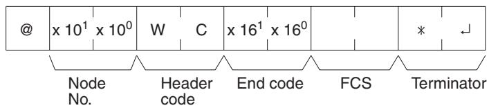
Parameters
Write Data (Command)
Specify in decimal numbers (BCD) the present values for the number of timers/counters that are to be written, starting from the beginning timer/counter.
Note
- When this command is used to write data to the PV area, the Completion Flags for the timers/counters that are written will be turned OFF.
- If data is specified for writing which exceeds the allowable range, an error will be generated and the writing operation will not be executed. If, for example, 510 is specified as the beginning word for writing, and three words of data are specified, then 512 will become the last word for writing data, and the command will not be executed because TC 512 is beyond area boundary.
6-5-13 TC STATUS WRITE — WG
Writes the status of the Completion Flags for timers and counters in the TC area, starting from the specified timer/counter (number). Writing is done number by number.
Command Format
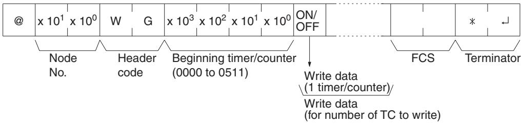
Note Divide the command when writing the status of more than 118 timer/counters.
Response Format
An end code of 00 indicates normal completion.
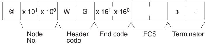
Parameters
Write Data (Command)
Specify the status of the Completion Flags, for the number of timers/counters to be written, in order (from the beginning word) as ON (i.e., "1") or OFF (i.e., "0"). When a Completion Flag is ON, it indicates that the time or count is up.
Note If data is specified for writing which exceeds the allowable range, an error will be generated and the writing operation will not be executed. If, for example, 510 is specified as the beginning word for writing, and three words of data are specified, then 512 will become the last word for writing data, and the command will not be executed because TC 512 is beyond area boundary.
6-5-14 DM AREA WRITE — WD
Writes data to the DM area, starting from the specified word. Writing is done word by word.
Command Format
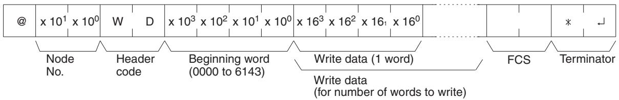
Note Divide the command when writing more than 29 words of data.
Response Format
An end code of 00 indicates normal completion.
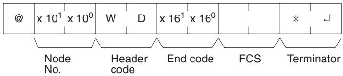
Parameters
Write Data (Command)
Specify in order the contents of the number of words to be written to the DM area in hexadecimal, starting with the specified beginning word.
Note
- If data is specified for writing which exceeds the allowable range, an error will be generated and the writing operation will not be executed. If, for example, 6142 is specified as the beginning word for writing, and three words of data are specified, then 6144 will become the last word for writing data, and the command will not be executed because DM 6144 is beyond the writable range.
- Be careful about the configuration of the DM area, as it varies depending on the CPU Unit model.
6-5-15 EM AREA WRITE — WE
Writes data to the specified EM area bank, starting from the specified word. Writing is done word by word.
Command Format
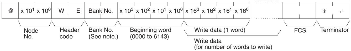
Note Input 00 Hex to specify bank number 0 or input two spaces to specify the current bank. Only the CQM1H-CPU61 CPU Unit has an EM area and it has only one bank, i.e., bank 0.
Response Format
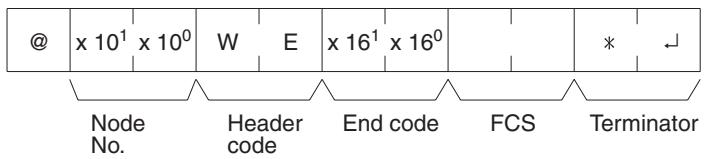
Parameters
Write Data (Command)
Specify in order the contents of the number of words to be written to the DM area in hexadecimal, starting with the specified beginning word.
Note
- If data is specified for writing which exceeds the allowable range, an error will be generated and the writing operation will not be executed. If, for example, 6142 is specified as the beginning word for writing, and three words of data are specified, then 6144 will become the last word for writing data, and the command will not be executed because DM 6144 is beyond the writable range.
- Be careful about the configuration of the DM area, as it varies depending on the CPU Unit model.
6-5-16 AR AREA WRITE — WJ
Writes data to the AR area, starting from the specified word. Writing is done word by word.
Command Format
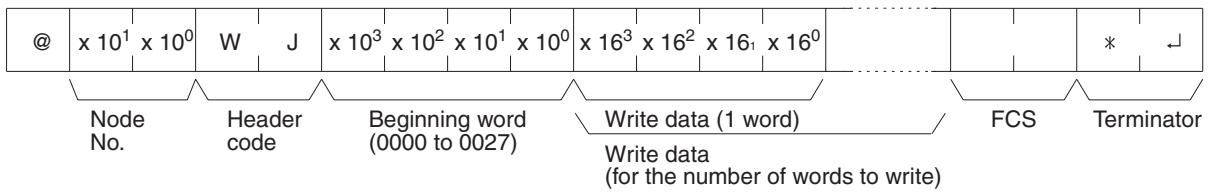
Response Format
An end code of 00 indicates normal completion.
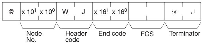
Parameters
Write Data (Command)
Specify in order the contents of the number of words to be written to the AR area in hexadecimal, starting with the specified beginning word.
Note If data is specified for writing which exceeds the allowable range, an error will be generated and the writing operation will not be executed. If, for example, 26 is specified as the beginning word for writing, and three words of data are specified, then 28 will become the last word for writing data, and the command will not be executed because AR 28 is beyond the writable range.
6-5-17 SV READ 1 — R#
Searches for the first instance of a TIM, TIMH(15), TTIM, CNT, and CNTR(12) instruction with the specified TC number in the user's program and reads the PV, which assumed to be set as a constant. The SV that is read is a 4-digit decimal number (BCD). The program is searched from the beginning, which may take as much as 10 seconds to produce a response.
Command Format
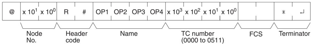
Response Format
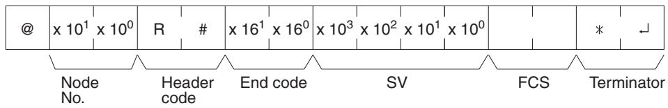
Parameters
Name, TC Number (Command)
Specify the instruction for reading the SV in "Name." Make this setting in 4 characters. In "TC number," specify the timer/counter number used for the instruction.
| Instruction name | Classification | |||
| OP1 | OP2 | OP3 | OP4 | |
| T | I | M | (Space) | TIMER |
| T | I | M | H | HIGH-SPEED TIMER |
| T | T | I | M | TOTALIZING TIMER |
| C | N | T | (Space) | COUNTER |
| C | N | T | R | REVERSIBLE COUNTER |
SV (Response)
The constant SV is returned.
Note
- The instruction specified under "Name" must be in four characters.
- If the same instruction is used more than once in a program, only the first one will be read.
- Use this command only when it is definite that a constant SV has been set.
- The response end code will indicate an error (16) if the SV wasn't entered as a constant.
6-5-18 SV READ 2 — R\$
Reads the constant SV or the word address where the SV is stored. The SV that is read is a 4-digit decimal number (BCD) written as the second operand for the TIM, TIMH(15), TTIM, CNT, or CNTR(12) instruction at the specified program address in the user's program. This can only be done with a program of less than 10,000.
Command Format
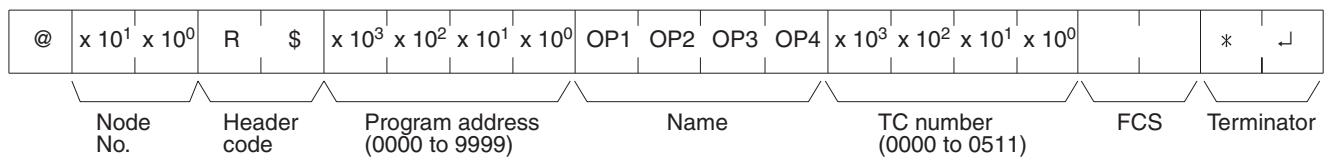
Response Format
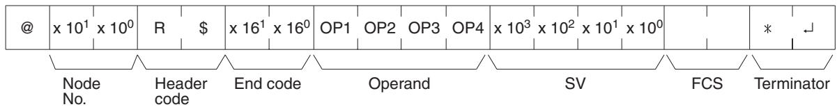
Parameters
Name, TC Number (Command)
Specify the name of the instruction for reading the SV in "Name." Make this setting in 4 characters. In "TC number," specify the timer/counter number used by the instruction.
| Instruction name | Classification | |||
| OP1 | OP2 | OP3 | OP4 | |
| T | I | M | (Space) | TIMER |
| T | I | M | H | HIGH-SPEED TIMER |
| T | T | I | M | TOTALIZING TIMER |
| C | N | T | (Space) | COUNTER |
| C | N | T | R | REVERSIBLE COUNTER |
Operand, SV (Response)
The name that indicates the SV classification is returned to “Operand,” and either the word address where the SV is stored or the constant SV is returned to “SV.”
| Operand | Classification | Constant or word address | |||
| OP1 | OP2 | OP3 | OP4 | ||
| C | I | O | (Space) | IR or SR | 0000 to 0255 |
| L | R | (Space) | (Space) | LR | 0000 to 0063 |
| H | R | (Space) | (Space) | HR | 0000 to 0099 |
| A | R | (Space) | (Space) | AR | 0000 to 0027 |
| D | M | (Space) | (Space) | DM | 0000 to 6655 |
| D | M | * | (Space) | DM (indirect) | 0000 to 6655 |
| E | M | (Space) | (Space) | EM | 0000 to 6143 |
| E | M | * | (Space) | EM (indirect) | 0000 to 6143 |
| C | O | N | (Space) | Constant | 0000 to 9999 |
Note
- The instruction name and operand area designations must be in four characters. Fill any gaps with spaces to make a total of four characters.
- Only the CQM1H-CPU61 CPU Unit has an EM area.
6-5-19 SV READ 3 — R%
Reads the constant SV or the word address where the SV is stored. The SV that is read is a 4-digit decimal number (BCD) written in the second word of the TIM, TIMH(15), TTIM, CNT, or CNTR(12) instruction at the specified program address in the user's program. With this command, program addresses can be specified for a program of up to 99,999 steps.
Command Format
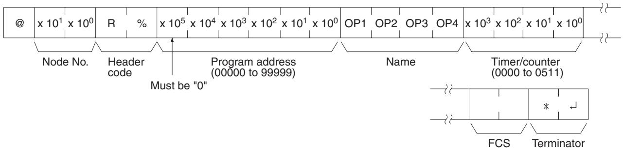
Response Format
An end code of 00 indicates normal completion.
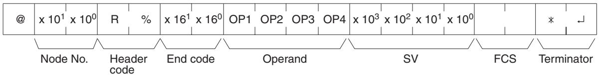
Parameters
Name, TC Number (Command)
Specify the name of the instruction for reading the SV in "Name." Make this setting in 4 characters. In "TC number," specify the timer/counter number used by the instruction.
| Instruction name | Classification | TC number range | |||
| OP1 | OP2 | OP3 | OP4 | ||
| T | I | M | (Space) | TIMER | 0000 to 0511 |
| T | I | M | H | HIGH-SPEED TIMER | |
| T | T | I | M | TOTALIZING TIMER | |
| C | N | T | (Space) | COUNTER | |
| C | N | T | R | REVERSIBLE COUNTER | |
Operand, SV (Response)
The name that indicates the SV classification is returned to “Operand,” and either the word address where the SV is stored or the constant SV is returned to “SV.”
| Operand | Classification | Constant or word address | |||
| OP1 | OP2 | OP3 | OP4 | ||
| C | I | O | (Space) | IR or SR | 0000 to 0255 |
| L | R | (Space) | (Space) | LR | 0000 to 0063 |
| H | R | (Space) | (Space) | HR | 0000 to 0099 |
| A | R | (Space) | (Space) | AR | 0000 to 0027 |
| D | M | (Space) | (Space) | DM | 0000 to 6655 |
| D | M | * | (Space) | DM (indirect) | 0000 to 6655 |
| E | M | (Space) | (Space) | EM | 0000 to 6143 |
| E | M | * | (Space) | EM (indirect) | 0000 to 6143 |
| C | O | N | (Space) | Constant | 0000 to 9999 |
Note
- The instruction name and operand area designations must be in four characters. Fill any gaps with spaces to make a total of four characters.
- Only the CQM1H-CPU61 CPU Unit has an EM area.
6-5-20 SV CHANGE 1 — W#
Searches for the first instance of the specified TIM, TIMH(15), TTIM, CNT, or CNTR(12) instruction in the user's program and changes the SV to new constant SV specified in the second word of the instruction. The program is searched from the beginning, and it may therefore take approximately 10 seconds to produce a response.
Command Format
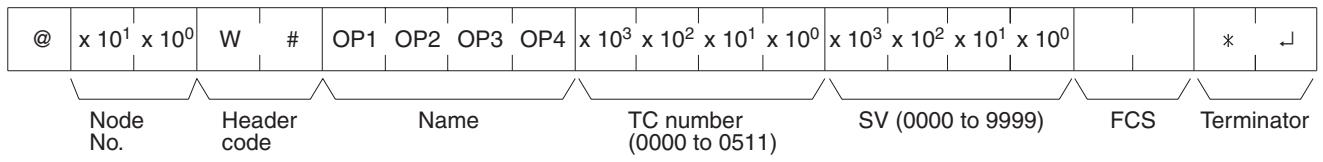
Response Format
An end code of 00 indicates normal completion.
Parameters
Name, TC Number (Command)
In “Name,” specify the name of the instruction, in four characters, for changing the SV. In “TC number,” specify the timer/counter number used for the instruction.
| Instruction name | Classification | |||
| OP1 | OP2 | OP3 | OP4 | |
| T | I | M | (Space) | TIMER |
| T | I | M | H | HIGH-SPEED TIMER |
| T | T | I | M | TOTALIZING TIMER |
| C | N | T | (Space) | COUNTER |
| C | N | T | R | REVERSIBLE COUNTER |
6-5-21 SV CHANGE 2 — W\$
Changes the contents of the second word of the TIM, TIMH(15), TTIM, CNT, or CNTR(12) at the specified program address in the user's program. This can only be done with a program of up to 9,999 steps.
Command Format
Response Format
An end code of 00 indicates normal completion.
Parameters
Name, TC Number (Command)
In “Name,” specify the name of the instruction, in four characters, for changing the SV. In “TC number,” specify the timer/counter number used for the instruction.
| Instruction name | Classification | |||
| OP1 | OP2 | OP3 | OP4 | |
| T | I | M | (Space) | TIMER |
| T | I | M | H | HIGH-SPEED TIMER |
| T | T | I | M | TOTALIZING TIMER |
| C | N | T | (Space) | COUNTER |
| C | N | T | R | REVERSIBLE COUNTER |
Operand, SV (Response)
In “Operand,” specify the name that indicates the SV classification. Specify the name in four characters. In “SV,” specify either the word address where the SV is stored or the constant SV.
| Operand | Classification | Constant or word address | |||
| OP1 | OP2 | OP3 | OP4 | ||
| C | I | O | (Space) | IR or SR | 0000 to 0252 |
| L | R | (Space) | (Space) | LR | 0000 to 0063 |
| H | R | (Space) | (Space) | HR | 0000 to 0099 |
| A | R | (Space) | (Space) | AR | 0000 to 0027 |
| D | M | (Space) | (Space) | DM | 0000 to 6655 |
| D | M | * | (Space) | DM (indirect) | 0000 to 6655 |
| E | M | (Space) | (Space) | EM | 0000 to 6143 |
| E | M | * | (Space) | EM (indirect) | 0000 to 6143 |
| C | O | N | (Space) | Constant | 0000 to 9999 |
Note Only the CQM1H-CPU61 CPU Unit has an EM area.
6-5-22 SV CHANGE 3 — W%
Changes the contents of the second word of the TIM, TIMH(15), TTIM CNT, or CNTR(12) at the specified program address in the user's program. With this command, program address can be specified for a program of up to 99,999 steps.
Command Format
Response Format
An end code of 00 indicates normal completion.
Parameters
Name, TC Number (Command)
In “Name,” specify the name of the instruction, in four characters, for changing the SV. In “TC number,” specify the timer/counter number used for the instruction.
| Instruction name | Classification | TC number range | |||
| OP1 | OP2 | OP3 | OP4 | ||
| T | I | M | (Space) | TIMER | 0000 to 0511 |
| T | I | M | H | HIGH-SPEED TIMER | |
| T | T | I | M | TOTALIZING TIMER | |
| C | N | T | (Space) | COUNTER | |
| C | N | T | R | REVERSIBLE COUNTER | |
Operand, SV (Response)
In “Operand,” specify the name that indicates the SV classification. Specify the name in four characters. In “SV,” specify either the word address where the SV is stored or the constant SV.
| Operand | Classification | Constant or word address | |||
| OP1 | OP2 | OP3 | OP4 | ||
| C | I | O | (Space) | IR or SR | 0000 to 0252 |
| L | R | (Space) | (Space) | LR | 0000 to 0063 |
| H | R | (Space) | (Space) | HR | 0000 to 0099 |
| A | R | (Space) | (Space) | AR | 0000 to 0027 |
| D | M | (Space) | (Space) | DM | 0000 to 6655 |
| D | M | * | (Space) | DM (indirect) | 0000 to 6655 |
| E | M | (Space) | (Space) | EM | 0000 to 6143 |
| E | M | * | (Space) | EM (indirect) | 0000 to 6143 |
| C | O | N | (Space) | Constant | 0000 to 9999 |
Note Only the CQM1H-CPU61 CPU Unit has an EM area.
6-5-23 STATUS READ — MS
Reads the PC operating conditions.
Command Format
Response Format
An end code of 00 indicates normal completion.
Parameters
Status Data, Message (Response)
“Status data” consists of four digits (two bytes) hexadecimal. The leftmost byte indicates CPU Unit operation mode, and the rightmost byte indicates the size of the program area.
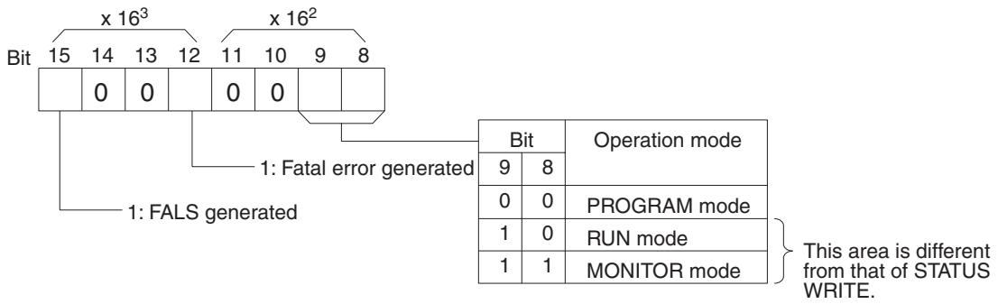
flowchart
graph TD
A["Bit 15"] --> B["0"]
C["Bit 14"] --> D["0"]
E["Bit 13"] --> F["0"]
G["Bit 12"] --> H["0"]
I["Bit 11"] --> J["0"]
K["Bit 10"] --> L["0"]
M["Bit 9"] --> N["0"]
O["Bit 8"] --> P["0"]
Q["Bit 1: Fatal error generated"] --> R["1: FALS generated"]
S["Bit 9"] --> T["8: Operation mode"]
U["Bit 0"] --> V["0: PROGRAM mode"]
W["Bit 1"] --> X["0: RUN mode"]
Y["Bit 1"] --> Z["1: MONITOR mode"]
style A fill:#f9f,stroke:#333
style C fill:#f9f,stroke:#333
style G fill:#f9f,stroke:#333
style I fill:#f9f,stroke:#333
style K fill:#f9f,stroke:#333
style M fill:#f9f,stroke:#333
style Q fill:#f9f,stroke:#333
style R fill:#ccf,stroke:#333
style U fill:#ccf,stroke:#333
style W fill:#ccf,stroke:#333
style Y fill:#ccf,stroke:#333
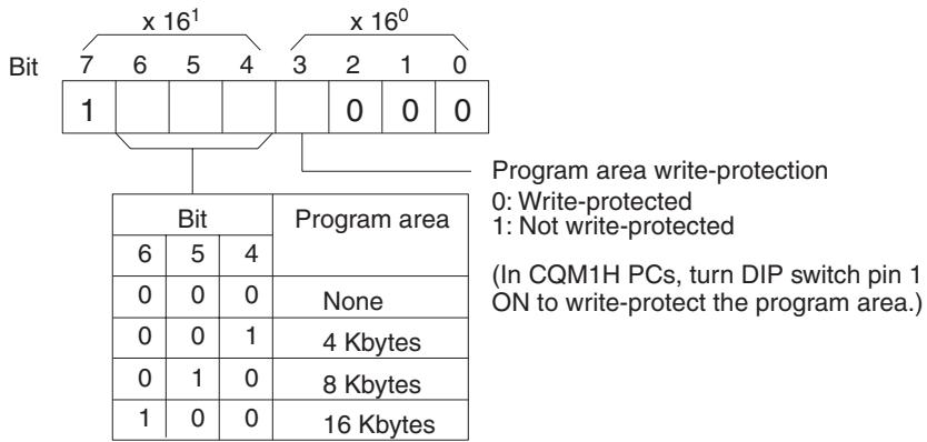
The “Message” parameter is a FAL/FALS number that exists when the command is executed. When there is no message, this parameter is omitted.
6-5-24 STATUS WRITE — SC
Changes the PC operating mode.
Command Format

Response Format
An end code of 00 indicates normal completion.
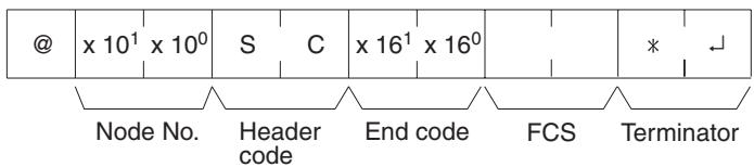
Parameters
Mode Data (Command)
“Mode data” consists of two digits (one byte) hexadecimal. With the leftmost two bits, specify the PC operating mode. Set all of the remaining bits to “0.”
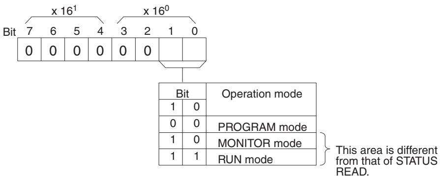
6-5-25 ERROR READ — MF
Reads and clears errors in the PC. Also checks whether previous errors have been cleared.
Command Format
Response Format
An end code of 00 indicates normal completion.
Parameters
Error Clear (Command)
Specify 01 to clear errors and 00 to not clear errors (BCD). Fatal errors can be cleared only when the PC is in PROGRAM mode.
Error Information (Response)
The error information comes in two words.
1st word
6-5-26 FORCED SET — KS
Force sets a bit in the IR, SR, LR, HR, AR, or TC area. Just one bit can be force set at a time.
Once a bit has been forced set or reset, that status will be retained until a FORCED SET/RESET CANCEL (KC) command or the next FORCED SET/RESET command is transmitted.
Command Format
Response Format
An end code of 00 indicates normal completion.
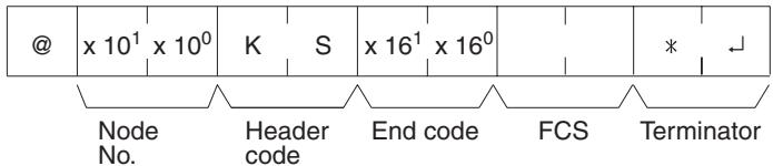
Parameters
Name, Word address, Bit (Command)
In “Name,” specify the area (i.e., IR, SR, LR, HR, AR, or TC) that is to be forced set. Specify the name in four characters. In “Word address,” specify the address of the word, and in “Bit” the number of the bit that is to be forced set.
| Name | Classification | Word address setting range | Bits | |||
| OP1 | OP2 | OP3 | OP4 | |||
| C | I | O | (Space) | IR or SR | 0000 to 0252 | 00 to 15 (decimal) |
| L | R | (Space) | (Space) | LR | 0000 to 0063 | |
| H | R | (Space) | (Space) | HR | 0000 to 0099 | |
| A | R | (Space) | (Space) | AR | 0000 to 0027 | |
| T | I | M | (Space) | Completion Flag (timer) | 0000 to 0511 | Always 00 |
| T | I | M | H | Completion Flag (high-speed timer) | ||
| T | T | I | M | Completion Flag (totalizing timer) | ||
| C | N | T | (Space) | Completion Flag (counter) | ||
| C | N | T | R | Completion Flag (reversible counter) | ||
Note The area specified under “Name” must be in four characters. Add spaces after the data area name if it is shorter than four characters.
6-5-27 FORCED RESET — KR
Force resets a bit in the IR, SR, LR, HR, AR, or TC area. Just one bit can be force reset at a time.
Once a bit has been forced set or reset, that status will be retained until a FORCED SET/RESET CANCEL (KC) command or the next FORCED SET/RESET command is transmitted.
Command Format

Response Format
An end code of 00 indicates normal completion.
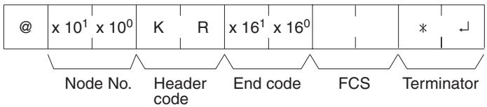
Parameters
Name, Word address, Bit (Command)
In “Name,” specify the area (i.e., IR, SR, LR, HR, AR, or TC) that is to be forced reset. Specify the name in four characters. In “Word address,” specify the address of the word, and in “Bit,” the number of the bit that is to be forced reset.
| Name | Classification | Word address setting range | Bits | |||
| OP1 | OP2 | OP3 | OP4 | |||
| C | I | O | (Space) | IR or SR | 0000 to 0252 | 00 to 15 (decimal) |
| L | R | (Space) | (Space) | LR | 0000 to 0063 | |
| H | R | (Space) | (Space) | HR | 0000 to 0099 | |
| A | R | (Space) | (Space) | AR | 0000 to 0027 | |
| T | I | M | (Space) | Completion Flag (timer) | 0000 to 0511 | Always 00 |
| T | I | M | H | Completion Flag (high-speed timer) | ||
| T | T | I | M | Completion Flag (totalizing timer) | ||
| C | N | T | (Space) | Completion Flag (counter) | ||
| C | N | T | R | Completion Flag (reversible counter) | ||
Note The area specified under “Name” must be in four characters. Add spaces after the data area name if it is shorter than four characters.
6-5-28 MULTIPLE FORCED SET/RESET — FK
Force sets, force resets, or cancels the status of the bits in one word in the IR, SR, LR, HR, AR, or TC area.
Command Format
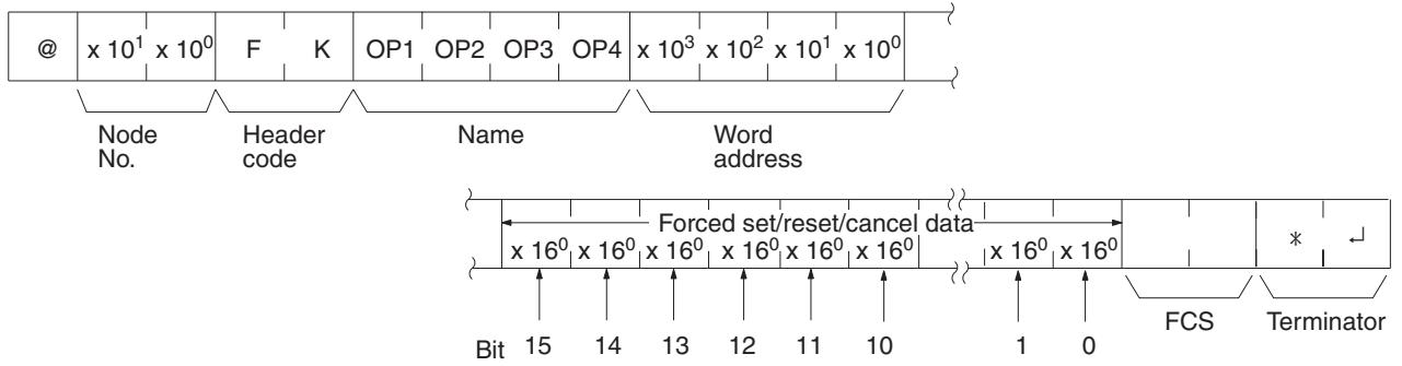
Response Format
An end code of 00 indicates normal completion.
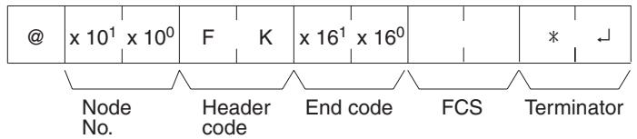
Parameters
Name, Word address (Command)
In “Name,” specify the area (i.e., IR, SR, LR, HR, AR, or TC) that is to be forced set or reset. Specify the name in four characters. In “Word address,” specify the address of the word that is to be forced set or reset.
| Name | Classification | Word address setting range | Bits | |||
| OP1 | OP2 | OP3 | OP4 | |||
| C | I | O | (Space) | IR or SR | 0000 to 0252 | 00 to 15 |
| L | R | (Space) | (Space) | LR | 0000 to 0063 | |
| H | R | (Space) | (Space) | HR | 0000 to 0099 | |
| A | R | (Space) | (Space) | AR | 0000 to 0027 | |
| T | I | M | (Space) | Completion Flag (timer) | 0000 to 0511 | Always 15 |
| T | I | M | H | Completion Flag (high-speed timer) | ||
| T | T | I | M | Completion Flag (totalizing timer) | ||
| C | N | T | (Space) | Completion Flag (counter) | ||
| C | N | T | R | Completion Flag (reversible counter) | ||
Forced set/Reset/Cancel data (Command)
If a timer or counter completion flag is specified, only bit 15 is effective and all other bits will be ignored. Only force-setting and force-resetting are possible for timers/counters.
If a word address is specified, the content of the word specifies the desired process for each bit in the specified word, as shown in the following table.
| BCD setting | Process |
| 0 | No action (bit status not changed) |
| 2 | Reset |
| 3 | Set |
| 4 | Forced-reset |
| 5 | Forced-set |
| 8 | Forced set/reset status cancel |
The bits that are merely set or reset may change status the next time the program is executed, but bits that are force-set or force-reset will maintain the forced status until it is cleared.
Response Format
An end code of 00 indicates normal completion.
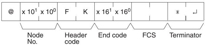
6-5-29 FORCED SET/RESET CANCEL — KC
Cancels all forced set and forced reset bits (including those set by FORCED SET, FORCED RESET, and MULTIPLE FORCED SET/RESET). If multiple bits are set, the forced status will be cancelled for all of them. It is not possible to cancel bits one by one using KC.
Command Format
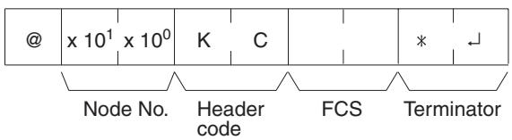
Response Format
An end code of 00 indicates normal completion.

6-5-30 PC MODEL READ — MM
Reads the model type of the PC.
Command Format
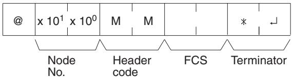
Response Format
An end code of 00 indicates normal completion.
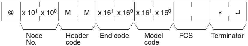
Parameters
Model Code
"Model code" indicates the PC model in two digits hexadecimal.
| Model code | Model |
| 01 | C250 |
| 02 | C500 |
| 03 | C120 |
| 0E | C2000 |
| 10 | C1000H |
| 11 | CQM1H/C2000H/CQM1/CPM1/CPM1A/CPM2A/CPM2C/SRM1 |
| 12 | C20H/C28H/C40H/C200H/C200HS |
| 20 | CV500 |
| 21 | CV1000 |
| 22 | CV2000 |
| 40 | CVM1-CPU01-E |
| 41 | CVM1-CPU11-E |
| 42 | CVM1-CPU21-E |
6-5-31 TEST—TS
Returns, unaltered, one block of data transmitted from the host computer.
Command Format
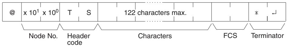
Response Format
An end code of 00 indicates normal completion.
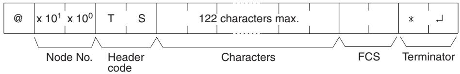
Parameters
Characters (Command, Response)
For the command, this setting specifies any characters other than the carriage return (CHR\$(13)). For the response, the same characters as specified by the command will be returned unaltered if the test is successful.
6-5-32 PROGRAM READ — RP
Reads the contents of the PC user's program area in machine language (object code). The contents are read as a block, from the beginning to the end.
Command Format
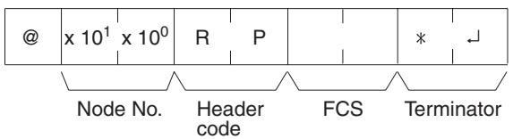
Response Format
An end code of 00 indicates normal completion.
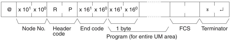
Parameters
Program (Response)
The program is read from the entire program area.
Note To stop this operation in progress, execute the ABORT (XZ) command.
6-5-33 PROGRAM WRITE — WP
Writes to the PC user's program area the machine language (object code) program transmitted from the host computer. The contents are written as a block, from the beginning.
Command Format
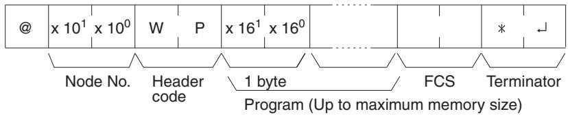
Response Format
An end code of 00 indicates normal completion.
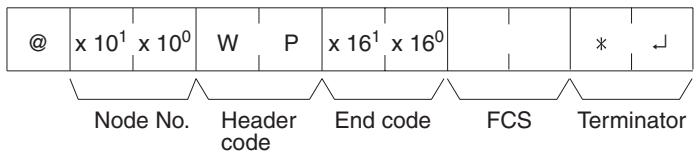
Parameters
Program (Command)
Program data up to the maximum memory size.
6-5-34 COMPOUND COMMAND — QQ
Registers at the PC all of the bits, words, and timers/counters that are to be read, and reads the status of all of them as a batch.
Registering Read Information
Register the information on all of the bits, words, and timers/counters that are to be read.
Command Format
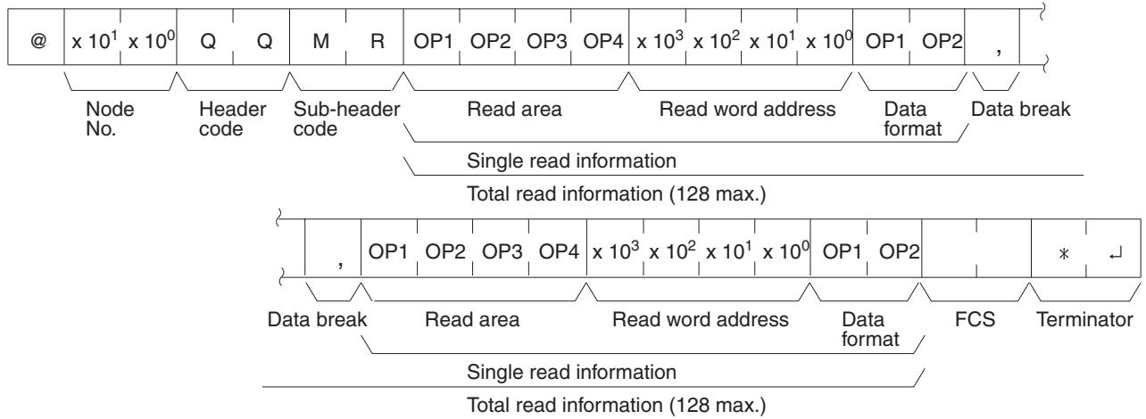
flowchart
graph TD
A["@"] --> B["x 10^1 x 10^0"]
B --> C["Q"]
C --> D["M"]
D --> E["R"]
E --> F["OP1"]
F --> G["OP2"]
G --> H["OP3"]
H --> I["OP4"]
I --> J["x 10^3 x 10^2 x 10^1 x 10^0"]
J --> K["OP1"]
K --> L["OP2"]
L --> M[","]
M --> N["Node No."]
M --> O["Header code"]
M --> P["Sub-header code"]
P --> Q["Read area"]
Q --> R["Read word address"]
R --> S["Data format"]
R --> T["Data break"]
U["Single read information"] --> V["Total read information (128 max.)"]
W[","] --> X["OP1"]
W --> Y["OP2"]
W --> Z["OP3"]
W --> AA["OP4"]
AA --> AB["x 10^3 x 10^2 x 10^1 x 10^0"]
AB --> AC["OP1"]
AB --> AD["OP2"]
AE["*"] --> AF["*"]
AG["Data break"] --> AH["Read area"]
AH --> AI["Read word address"]
AI --> AJ["Data format"]
AK["FCS"] --> AL["Terminator"]
AM["Single read information"] --> AN["Total read information (128 max.)"]
Response Format
An end code of 00 indicates normal completion.
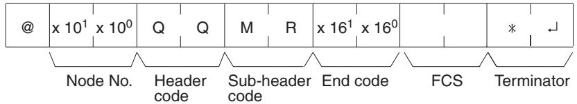
Parameters
Read Area (Command)
Specify in four-character code the area that is to be read. The codes that can be specified are listed in the following table.
Read Word address, Data Format (Command)
Depending on the area and type of data that are to be read, the information to be read is as shown in the following table. The “read data” is specified in four digits BCD, and the data format is specified in two digits BCD.
| Area | Read data | Read area | Read word | Data format |
| IR or SR | Bit | C I O (S) | 0000 to 0255 | 00 to 15 (decimal) |
| Word | “CH” | |||
| LR | Bit | L R (S) (S) | 0000 to 0063 | 00 to 15 (decimal) |
| Word | “CH” | |||
| HR | Bit | H R (S) (S) | 0000 to 0099 | 00 to 15 (decimal) |
| Word | “CH” | |||
| AR | Bit | A R (S) (S) | 0000 to 0027 | 00 to 15 (decimal) |
| Bit | “CH” | |||
| Timer | Completion Flag | T I M (S) | 0000 to 0511 | 2 characters other than “CH” |
| PV | “CH” | |||
| High-speed timer | Completion Flag | T I M H | 0000 to 0511 | 2 characters other than “CH” |
| PV | “CH” | |||
| Totalizing timer | Completion Flag | T T I M | 0000 to 0511 | 2 characters other than “CH” |
| PV | “CH” | |||
| Counter | Completion Flag | C N T (S) | 0000 to 0511 | 2 characters other than “CH” |
| PV | “CH” | |||
| Reversible counter | Completion Flag | C N T R | 0000 to 0511 | 2 characters other than “CH” |
| PV | “CH” | |||
| DM | Word | D M (S) (S) | 0000 to 6655 | Any 2 characters |
| EM | Word in current bank | E M (S) (S) | 0000 to 6143 | Any 2 characters |
| Word in specified bank | E M 00 |
Note Only the CQM1H-CPU61 CPU Unit has an EM area.
(S): Space
Data Break (Command)
The read information is specified one item at a time separated by a break code (,). The maximum number of items that can be specified is 128. (When the PV of a timer/counter is specified, however, the status of the Completion Flag is also returned, and must therefore be counted as two items.)
Batch Reading
The bit, word, and timer/counter status is read as a batch according to the read information that was registered with QQ.
Command Format
Response Format
An end code of 00 indicates normal completion.
Parameters
Read Data (Response)
Read data is returned according to the data format and the order in which read information was registered using QQ. If “Completion Flag” has been specified, then bit data (ON or OFF) is returned. If “Word” has been specified, then word data is returned. If “PV” has been specified for timers/counters, however, then the PV is returned following the Completion Flag.
Data Break (Response)
The break code (,) is returned between sections that are read.
6-5-35 ABORT — XZ
Aborts the Host Link operation that is currently being processed, and then enables reception of the next command. The ABORT command does not receive a response.
Command Format
6-5-36 INITIALIZE — \*\*
Initializes the transmission control procedure of all the PCs connected to the host computer. The INITIALIZE command does not use node numbers or FCS, and does not receive a response.
Command Format

6-5-37 TXD RESPONSE — EX
This is the response format used when the PC's TXD(—) instruction is executed in Host Link mode. (TXD(—) converts the specified data into ASCII code and transmits it to the host computer with this format.)
Response Format

Parameters
Characters (Response)
The frame can contain up to 122 characters. TXD(48) does not support multiple frames.
End Codes
There are no end codes with this command.
6-5-38 Undefined Command — IC
This response is returned if the header code of a command cannot be decoded. Check the header code.
Response Format
SECTION 7
CPU Unit Operation and Processing Time
This section explains the internal processing of the CQM1H CPU Unit, and the time required for processing and execution. Refer to this section to gain an understanding of the precise timing of CQM1H operation.
7-1 CPU Unit Operation 474
7-2 Power Interruptions.... 475
7-2-1 Operation at Power Interruption 475
7-2-2 Startup Operation after a Power Interruption 477
7-3 Cycle Time 478
7-3-1 Overview.... 478
7-3-2 Instruction Execution Times.... 479
7-3-3 I/O Response Time 491
7-3-4 One-to-one Link I/O Response Time 493
7-3-5 Interrupt Processing Time.... 495
7-1 CPU Unit Operation
Operation Flowchart
The overall flow of CQM1H operation is as shown in the following flowchart. The time required to execute one cycle of CPU Unit operation is called the cycle time.
flowchart
graph TD
A["Power application"] --> B{Is DIP switch pin 2 ON?}
B -->|OFF| C["Transfer contents of Memory Cassette to CPU Unit"]
B -->|ON| D["Clear IR, SR, AR areas; preset timers; and check I/O Units, Inner Boards and Communications Units"]
C --> D
D --> E["Check hardware and Program Memory"]
E --> F{Check OK?}
F -->|No| G{ERROR or ALARM?}
F -->|Yes| H["Service Inner Boards with control functions. (See note 1.)"]
H --> I["Preset cycle time monitoring time"]
I --> J["Execute user's program"]
J --> K{End of program?}
K -->|No| L["Check cycle time setting"]
K -->|Yes| M{Minimum cycle time?}
M -->|No| N["Wait until minimum cycle time expires"]
M -->|Yes| O["Compute cycle time"]
O --> P["Refresh input bits and output terminals"]
P --> Q["Service RS-232C port"]
Q --> R["Service peripheral port"]
R --> S["Service Inner Boards with communications functions (See note 2.)"]
S --> T["Service Communications Unit"]
T --> U["Initialization"]
U --> V["Overseeing processes"]
V --> W["Program execution"]
W --> X["Cycle time processing"]
X --> Y["I/O refreshing"]
Y --> Z["Service RS-232C interface"]
Z --> AA["Service peripheral port"]
AA --> AB["Service Inner Boards (communications)"]
AB --> AC["Service Communications Unit"]
AC --> AD["Ordering"]
AD --> AE["Set error flags and activate indicators."]
AE --> AF{ALARM (flashing)}
AF -->|No| AG["Error or ALARM?"]
AG --> AH["Error (lit)"]
Note
- Servicing Inner Boards with control functions involves transferring data between the CPU Unit and High-speed Counter, Pulse I/O, Absolute Encoder Interface, Analog Setting, and Analog I/O Boards.
- Servicing Inner Boards with communications functions involves transferring data between the CPU Unit and the Serial Communications Boards.
I/O Refresh Methods
CQM1H I/O refresh operations are broadly divided into two categories. The first of these, input refresh, involves reading the ON/OFF status of input points to the input bits. The second, output refresh, involves writing the ON/OFF status after program execution to the output points. The CQM1H I/O refresh methods are as shown in the following table.
| Input/Output | I/O refresh method | Function |
| Input | Cyclic refresh | Input refresh is executed at a set time once per cycle. |
| Interrupt input refresh | Input refresh is executed before execution of the interrupt routine whenever an input interrupt, interval timer interrupt, or high-speed counter interrupt occurs. (The cyclic refresh is also executed.) | |
| Output | Cyclic refresh | Output refresh is executed at a set time once per cycle. |
| Direct refresh | When there is an output from the user's program, that output point is immediately refreshed. (The cyclic refresh is also executed.) |
The default settings for I/O refreshing are as follows:
Inputs: Only cyclic refresh executed.
Outputs: Only cyclic refresh executed.
Cyclic refreshing must be executed for both inputs and outputs. Input refreshing at interrupts can be enabled by setting the input refresh range in the PC Setup (DM 6630 to DM 6638). Direct refreshing can be enabled using the setting in DM 6639 of the PC Setup.
In addition to the methods described above, it is also possible to execute I/O refreshes from the ladder program by means of IORF(97).
7-2 Power Interruptions
7-2-1 Operation at Power Interruption
The following processing is performed if CPU Unit power is interrupted. The following processing will be performed if the power supply falls below 85% of the rated voltage while the CPU Unit is in RUN or MONITOR mode.
1,2,3...
- The CPU Unit will stop.
- Outputs from all Output Units will be turned OFF.
Note All outputs will turn OFF regardless of the status of the I/O Hold Bit or the setting of the I/O Hold Bit Status setting in the PC Setup.
85% of the Rated Voltage:
AC power: 85 V for a 100-V AC system and 170 V for a 200-V AC system
DC power: 19.2 V DC
The following processing will be performed for a momentary power interruption.
1,2,3...
-
The system will continue to run unconditionally if the power interruption (i.e., the period during which the voltage is less than 85% of the rated voltage) lasts less than 10 ms for AC power supply, or 5 ms for DC power supply.
-
A power interruption may or may not be detected for a power interruption that lasts more than 10 ms but less than 25 ms for AC power supply, or more than 5 ms but less than 25 ms for DC power supply, i.e., the system may continue or it may stop.
- The system will stop unconditionally if the power interruption lasts more than 25 ms for either AC or DC power supply.
other
| Signal Type | Event Description | | -------------------------------- | ------------------------------------- | | Power OFF detected | Operation always stopped at this point regardless. | | Power OFF Detection Time | AC: 5 to 10 ms | | Power OFF Detection Time | DC: 10 to 25 ms | | 5-V internal power supply | Power OFF Detection Time | | Program execution | Executed | | Program execution | Stopped | | CPU reset signal | Stamped |7-2-2 Startup Operation after a Power Interruption
CPU Unit will operate in the following way when power is supplied after a power interruption. The time required for operation to resume after the power supply is restored will depend on the power supply voltage, configuration, ambient temperature, program contents, and other conditions.
The CPU Unit will start operating in RUN or MONITOR mode in any one of the following cases:
- DM 6600 (Startup Mode) is at the default setting, nothing is connected to the peripheral port, and pin 7 on the DIP switch on the CPU Unit is ON.
- DM 6600 (Startup Mode) is set to 0202 Hex (RUN mode) or 0201 Hex (MONITOR mode).
- The Programming Console is connected and its mode selector is set to RUN or MONITOR mode. (DM 6600 must be at the default setting.)
The operation at that time will be as follows (refer to the CQM1H Operation Manual for details on the operating mode at startup):
When the (AC or DC) power supply is restored (i.e., becomes more than 85% of the rated voltage), the CPU Unit will start operating approx. 500 ms after the 5-V internal power supply has been restored. The following timing chart illustrated this.
other
| Signal Type | Status | Approx. 500 ms | | ------------------------------- | ------------ | -------------- | | Power OFF detected signal | Yes | - | | 5-V internal power supply | Yes | - | | CPU reset signal | Yes | - | | Program execution status | - | - |7-3 Cycle Time
7-3-1 Overview
The processes involved in a single execution cycle are shown in the following table, and their respective processing times are explained.
| Process | Content | Time requirements |
| Overseeing | Setting cycle watchdog timer, I/O bus check, UM check, refreshing clock, refreshing bits in SR and AR areas, servicing Inner Boards with control functions (CQM1H-CPU61 only. See note 1.) etc. | 0.7 ms (0.1 ms when a Memory Cassette equipped with a clock is mounted)Add an additional 0.1 ms for each Inner Board (not including a Serial Communications Board). If there are no Inner Boards, no additional time is required. |
| Program execution | User program is executed. | Total time for executing instructions. (Varies according to content of user's program.) |
| Cycle time calculation | Standby until set time, when minimum cycle time is set in DM 6619 of PC Setup.Calculation of cycle time. | Almost instantaneous, except for standby processing. |
| I/O refresh | Input Unit's input information is read to input bits.Output information (results of executing program) is written to Output Unit's output bits. | Number of input words × 0.01 msNumber of output words × 0.005 ms |
| RS-232C port servicing | Devices connected to RS-232C port serviced.(Except for CQM1H-CPU11.) | 5% or less of cycle time (see note 3) |
| Peripheral port servicing | Devices connected to peripheral port serviced. | 5% or less of cycle time (see note 3) |
| Inner Board with communications functions servicing (See note 2.) | When a Serial Communications Board is mounted, commands from the Board are processed.(CQM1H-CPU51/61 only.) | 0.4 ms + processing time per portThe processing time per port is the minimum of 0.256 or 0.05 × cycle time calculated above.If there is no Serial Communications Board mounted, this time will be 0 ms. |
| Communications Unit servicing | When a Controller Link Unit is mounted, commands from the Board are processed. (CQM1H-CPU51/61 only.) | For the CQM1H-CLK21, 4 ms max.If a Communications Unit is not connected, this time will be 0 ms. |
Note
- Servicing Inner Boards with control functions involves transferring data between the CPU Unit and High-speed Counter, Pulse I/O, Absolute Encoder Interface, Analog Setting, and Analog I/O Boards.
- Servicing Inner Boards with communications functions involves transferring data between the CPU Unit and a Serial Communications Board.
- The percentages can be changed in the PC Setup (DM 6616: Servicing time for RS-232C port, DM 6617: Servicing time for peripheral port). When the RS-232C port, peripheral port, or Serial Communications Board port 1 or 2 is used, the time will be 0.256 min. per port.
Cycle Time and Operation
The effects of the cycle time on CPU Unit operation are as shown below.
| Cycle time | Operation conditions |
| 10 ms or longer | TIMH(15) may be inaccurate when TC 016 through TC 511 are used (operation will be normal for TC 000 through TC 015) (see note 1). |
| 20 ms or longer | Programming using the 0.02-second Clock Bit (SR 25401) may be inaccurate. |
| 100 ms or longer | Programming using the 0.1-second Clock Bit (SR 25500) may be inaccurate. A CYCLE TIME OVER error is generated (SR 25309 will turn ON) (see note 2).The TIMER (TIM) and TOTALIZING TIMER (TTIM) instructions may not be accurate. |
| 120 ms or longer | The FALS 9F monitoring time SV is exceeded. A system error (FALS 9F) is generated, and operation stops (see note 3). |
| 200 ms or longer | Programming using the 0.2-second Clock Bit (SR 25501) may be inaccurate. |
Note
- The number of timers to undergo interrupt processing can be set in DM 6629 of the PC Setup. The default setting is for TC 000 through TC 015.
- The PC Setup (DM 6655) can be used to disable detection of CYCLE TIME OVER error.
- The FALS 9F cycle monitoring time can be changed by means of the PC Setup (DM 6618).
Cycle Time Example
In this example, the cycle time is calculated for a CQM1H with 80 I/O points. The I/O is configured as follows:
DC inputs: 48 points (3 words)
Bit outputs: 32 points (2 words)
The rest of the operating conditions are assumed to be as follows:
| User’s program: | 2,000 instructions(consisting of LD and OUT instructions) |
| Inner Boards: | Serial Communications Board and High-speed Counter Board |
| Communications Units: | No Controller Link Unit |
| Clock: | None |
| RS-232C port: | Used |
| Cycle time: | Variable (no minimum set) |
Note The average processing time for a single instruction in the user's program is assumed to be 0.625 s.
The cycle times are as shown in the following table.
| Process | Calculation method | Time with peripheral device | Time without peripheral device |
| Overseeing | Fixed | 0.8 ms | 0.8 ms |
| Program execution | 0.625 × 2000 (μs) | 1.25 ms | 1.25 ms |
| Cycle time calculation | Negligible | 0 ms | 0 ms |
| I/O refresh | 0.01 × 3 + 0.005 × 2 (μs) | 0.04 ms | 0.04 ms |
| RS-232C port servicing | 0 ms | 0 ms | |
| Peripheral port servicing | Minimum time | 0.34 ms | 0 ms |
| Serial Communications Board servicing | 0.4 + 0.26 (ms) | 0.66 ms | 0.66 ms |
| Communications Unit servicing | 0 ms | 0 ms | 0 ms |
| Cycle time | (1) + (2) + (3) + (4) + (5) + (6) | 3.27 ms | 3.01 ms |
Note
- The cycle time can be automatically read from the PC via a Peripheral Device.
- The maximum and current cycle time are stored in AR 26 and AR 27.
- The cycle time can vary with actual operating conditions and will not necessarily agree precisely with the calculated value.
- The RS-232C and peripheral port service time will be 0.256 ms minimum, 65.536 ms maximum.
7-3-2 Instruction Execution Times
The following table lists the execution times for CQM1H instructions. The maximum and minimum execution times and the conditions which cause them are given where relevant. When “word” is referred to in the Conditions column, it implies the content of any word except for indirectly addressed DM words. Indirectly addressed DM words, which create longer execution times when used, are indicated by “*DM.”
Execution times for most instructions depend on whether they are executed with an ON or an OFF execution condition. Exceptions are the ladder diagram instructions OUT and OUT NOT, which require the same time regardless of the execution condition. The OFF execution time for an instruction can also vary depending on the circumstances, i.e., whether it is in an interlocked program section and the execution condition for IL is OFF, whether it is between JMP(04) and JME(05) and the execution condition for JMP(04) is OFF, or whether it is reset by an OFF execution condition. "RSET," "IL," and "JMP" are used to indicate these three times.
Basic Instructions
| Code | Mnemonic | ON execution time (μs) | Conditions (Top: min.; bottom: max.) | OFF execution time (μs) | ||
| RSET | IL | JMP | ||||
| --- | LD | 0.375 | Any | --- | ||
| --- | LD NOT | --- | ||||
| --- | AND | |||||
| --- | AND NOT | |||||
| --- | OR | |||||
| --- | OR NOT | |||||
| --- | AND LD | |||||
| --- | OR LD | |||||
| --- | OUT | 0.563 | Without direct outputs or for operands other than IR 10000 to IR 11515 when direct outputs are used. | --- | ||
| --- | OUT NOT | |||||
| --- | SET | 0.938 | Direct outputs | --- | ||
| --- | RSET | |||||
| --- | TIM | 1.125 | Constant for SV | 1.125 | 1.125 | 1.125 |
| *DM for SV | 40.8 | 1.125 | 1.125 | |||
| --- | CNT | 1.125 | Constant for SV | 1.125 | 1.125 | 1.125 |
| *DM for SV | 38.7 | 1.125 | 1.125 | |||
Special Instructions
| Code | Mnemonic | ON execution time (μs) | Conditions (Top: min.; bottom: max.) | OFF execution time (μs) | ||
| 00 | NOP | 0.375 | Any | --- | ||
| 01 | END | 28.0 | --- | |||
| 02 | IL | 9.3 | 8.2 | |||
| 03 | ILC | 8.5 | 8.5 | |||
| 04 | JMP | 13.8 | 8.9 | |||
| 05 | JME | 8.3 | 8.3 | |||
| 06 | FAL | 42.6 | 1.125 | |||
| 07 | FALS | 3.0 | 1.125 | |||
| 08 | STEP | 43.7 | 1.125 | |||
| 09 | SNXT | 18.8 | 1.125 | |||
| 10 | SFT | 33.2 | With 1-word shift register | Reset | IL | JMP |
| 32.4 | 11.5 | 11.5 | ||||
| 58.3 | With 10-word shift register | 52.0 | 11.5 | 11.5 | ||
| 311.4 | With 100-word shift register | 241.0 | 11.5 | 11.5 | ||
| 11 | KEEP | 0.563 | Without direct outputs or for operands other than IR 10000 to IR 11515 when direct outputs are used. | --- | ||
| 0.938 | Direct outputs using IR 10000 to IR 11515 | |||||
| 12 | CNTR | 39.8 | Constant for SV | Reset | IL | JMP |
| 25.0 | 15.5 | 15.5 | ||||
| 59.7 | *DM for SV | |||||
| 13 | DIFU | 16.2 | Any | Normal | IL | JMP |
| 15.8 | 15.5 | 13.4 | ||||
| 14 | DIFD | 15.6 | Any | Normal | IL | JMP |
| 15.6 | 15.5 | 13.3 | ||||
| 15 | TIMH | 27.4 | Constant for SV | Reset | IL | JMP |
| 41.2 | 40.0 | 20.8 | ||||
| 27.4 | *DM for SV | 60.6 | 59.4 | 20.8 | ||
| 16 | WSFT | 33.6 | With 1-word shift register | 1.5 | ||
| 57.8 | With 10-word shift register | |||||
| 1.7 ms | With 1,024-word shift register using *DM | |||||
| 9.8 ms | With 6,144-word shift register using *DM | |||||
| 20 | CMP | 20.1 | When comparing a constant to a word | 1.5 | ||
| 22.2 | When comparing two words | |||||
| 58.0 | When comparing two *DM | |||||
| 21 | MOV | 17.7 | When transferring a constant to a word | 1.5 | ||
| 19.8 | When moving from one word to another | |||||
| 54.6 | When transferring *DM to *DM | |||||
| 22 | MVN | 17.8 | When transferring a constant to a word | 1.5 | ||
| 19.9 | When moving from one word to another | |||||
| 54.5 | When transferring *DM to *DM | |||||
| 23 | BIN | 37.8 | When converting a word to a word | 1.5 | ||
| 72.0 | When converting *DM to *DM | |||||
| 24 | BCD | 35.8 | When converting a word to a word | 1.5 | ||
| 70.0 | When converting *DM to *DM | |||||
| 25 | ASL | 18.0 | When shifting a word | 1.125 | ||
| 34.4 | When shifting *DM | |||||
| 26 | ASR | 18.0 | When shifting a word | 1.125 | ||
| 34.4 | When shifting *DM | |||||
| 27 | ROL | 18.6 | When rotating a word | 1.125 | ||
| 35.0 | When rotating *DM | |||||
| 28 | ROR | 18.6 | When rotating a word | 1.125 | ||
| 35.0 | When rotating *DM | |||||
| 29 | COM | 19.5 | When inverting a word | 1.125 | ||
| 36.3 | When inverting *DM | |||||
| 30 | ADD | 37.5 | Constant + word → word | 1.875 | ||
| 39.9 | Word + word → word | |||||
| 91.6 | *DM + *DM → *DM | |||||
| 31 | SUB | 37.5 | Constant - word → word | 1.875 | ||
| 39.8 | Word - word → word | |||||
| 91.6 | *DM - *DM → *DM | |||||
| 32 | MUL | 55.3 | Constant × word → word | 1.875 | ||
| 57.8 | Word × word → word | |||||
| 108.4 | *DM × *DM → *DM | |||||
| 33 | DIV | 54.2 | Word ÷ constant → word | 1.875 | ||
| 56.6 | word ÷ word → word | |||||
| 107.3 | *DM ÷ *DM → *DM | |||||
| 34 | ANDW | 31.5 | Constant ∩ word → word | 1.875 | ||
| 33.9 | Word ∩ word → word | |||||
| 85.6 | *DM ∩ *DM → *DM | |||||
| Code | Mnemonic | ON execution time (μs) | Conditions (Top: min.; bottom: max.) | OFF execution time (μs) | ||
| 35 | ORW | 31.5 | Constant V word → word | 1.875 | ||
| 33.9 | Word V word → word | |||||
| 85.6 | *DM V *DM → *DM | |||||
| 36 | XORW | 31.5 | Constant ¥ word → word | 1.875 | ||
| 33.9 | Word ¥ word → word | |||||
| 85.6 | *DM ¥ *DM → *DM | |||||
| 37 | XNRW | 31.5 | Constant ¥ word → word | 1.875 | ||
| 33.9 | Word ¥ word → word | |||||
| 85.6 | *DM ¥ *DM → *DM | |||||
| 38 | INC | 20.9 | When incrementing a word | 1.125 | ||
| 37.6 | When incrementing *DM | |||||
| 39 | DEC | 21.3 | When decrementing a word | 1.125 | ||
| 38.1 | When decrementing *DM | |||||
| 40 | STC | 9.0 | Any | 0.75 | ||
| 41 | CLC | 9.0 | 0.75 | |||
| 45 | TRSM | 21.6 | 0.75 | |||
| 46 | MSG | 18.5 | With message in words | 1.125 | ||
| 36.3 | With message in *DM | |||||
| 50 | ADB | 40.1 | Constant + word → word | 1.875 | ||
| 42.5 | Word + word → word | |||||
| 94.2 | *DM + *DM → *DM | |||||
| 51 | SBB | 40.1 | Constant - word → word | 1.875 | ||
| 42.5 | Word - word → word | |||||
| 94.2 | *DM - *DM → *DM | |||||
| 52 | MLB | 34.3 | Constant × word → word | 1.875 | ||
| 36.7 | Word × word → word | |||||
| 87.3 | *DM × *DM → *DM | |||||
| 53 | DVB | 35.1 | Word ÷ constant → word | 1.875 | ||
| 37.5 | Word ÷ word → word | |||||
| 88.1 | *DM ÷ *DM → *DM | |||||
| 54 | ADDL | 44.5 | Word + word → word | 1.875 | ||
| 96.7 | *DM + *DM → *DM | |||||
| 55 | SUBL | 44.5 | Word - word → word | 1.875 | ||
| 96.7 | *DM - *DM → *DM | |||||
| 56 | MULL | 153.4 | Word × word → word | 1.875 | ||
| 203.4 | *DM × *DM → *DM | |||||
| 57 | DIVL | 154.5 | Word ÷ word → word | 1.875 | ||
| 204.5 | *DM ÷ *DM → *DM | |||||
| 58 | BINL | 57.0 | Word → word | 1.5 | ||
| 90.5 | *DM → *DM | |||||
| 59 | BCDL | 45.7 | Word → word | 1.5 | ||
| 79.2 | *DM → *DM | |||||
| 70 | XFER | 54.7 | When transferring a constant to a word | 1.875 | ||
| 57.1 | When transferring a word to a word | |||||
| 2.2 ms | When transferring 1,024 words using *DM | |||||
| 12.5 ms | When transferring 6,144 words using *DM | |||||
| 71 | BSET | 34.2 | When setting a constant to 1 word | 1.875 | ||
| 58.5 | When setting word constant to 10 words | |||||
| 1.47 ms | When setting *DM to 1,024 words | |||||
| 8.22 ms | When setting *DM to 6,144 words | |||||
| 72 | ROOT | 48.0 | Word calculation → word | 1.5 | ||
| 83.1 | *DM calculation → *DM | |||||
| 73 | XCHG | 30.7 | Word → word | 1.5 | ||
| 64.2 | *DM → *DM | |||||
| 74 | SLD | 30.9 | Shifting 1 word | 1.5 | ||
| 76.5 | Shifting 10 word | |||||
| 4.12 ms | Shifting 1024 words using *DM | |||||
| 24.44 ms | Shifting 6144 words using *DM | |||||
| 75 | SRD | 30.9 | Shifting 1 word | 1.5 | ||
| 76.5 | Shifting 10 word | |||||
| 4.12 ms | Shifting 1,024 words using *DM | |||||
| 24.44 ms | Shifting 6,144 words using *DM | |||||
| 76 | MLPX | 44.4 | When decoding word to word | 1.875 | ||
| 102.3 | When decoding *DM to *DM | |||||
| 77 | DMPX | 33.9 | When encoding word to word | 1.875 | ||
| 90.5 | When encoding *DM to *DM | |||||
| 78 | SDEC | 45.5 | When decoding word to word | 1.875 | ||
| 103.9 | When decoding *DM to *DM | |||||
| 80 | DIST | 49.5 | When setting a constant to a word + a word | 1.875 | ||
| 52.0 | When setting a word to a word + a word | |||||
| 108.3 | When setting *DM to *DM +*DM | |||||
| 75.8 | When setting a constant to a stack | |||||
| 78.3 | When setting a word to a stack | |||||
| 133.4 | When setting *DM to a stack via *DM | |||||
| 81 | COLL | 48.9 | When setting a constant + a word to a word | 1.875 | ||
| 51.3 | When setting a word + a word to a word | |||||
| 105.1 | When setting *DM + *DM to *DM | |||||
| 45.9 | When setting a word + constant to FIFO stack | |||||
| 48.3 | When setting a word + word to FIFO stack | |||||
| 103.2 | When setting a *DM + *DM to FIFO stack via *DM | |||||
| 45.3 | When setting a word + constant to LIFO stack | |||||
| 47.7 | When setting a word + word to LIFO stack | |||||
| 102.6 | When setting a *DM + *DM to LIFO stack via *DM | |||||
| 82 | MOVB | 34.8 | When moving constant to word | 1.875 | ||
| 41.2 | When moving word to word | |||||
| 93.9 | When moving *DM to *DM | |||||
| 83 | MOVD | 30.6 | When moving constant to word | 1.875 | ||
| 36.9 | When moving word to word | |||||
| 89.6 | When moving *DM to *DM | |||||
| 84 | SFTR | 43.1 | Shifting 1 word | 1.875 | ||
| 73.8 | Shifting 10 word | |||||
| 1.7 ms | Shifting 1,024 words using *DM | |||||
| 9.68 ms | Shifting 6,144 words using *DM | |||||
| 85 | TCMP | 71.9 | Comparing constant to word-set table | 1.875 | ||
| 74.1 | Comparing word to word-set table | |||||
| 126.8 | Comparing *DM to *DM-set table | |||||
| 86 | ASC | 46.9 | Word → word | 1.875 | ||
| 108.3 | *DM → *DM | |||||
| 90 | SEND | 65.6 | Word | 1.875 | ||
| 121.4 | *DM | |||||
| 91 | SBS | 31.1 | Any | 1.125 | ||
| 92 | SBN | --- | --- | |||
| 93 | RET | 29.3 | 1.125 | |||
| 97 | IORF | 29.1 | Refreshing IR 000 | 1.5 | ||
| 35.0 | Refreshing one input word | |||||
| 39.0 | Refreshing one output word | |||||
| 93.3 | Refreshing 8 I/O words | |||||
| 98 | RECV | 78.4 | Word | 1.875 | ||
| 132.4 | *DM | |||||
| 99 | MCRO | 105.2 | With word-set I/O operands | 1.875 | ||
| 141.1 | With *DM-set I/O operands | |||||
Expansion Instructions
| Code | Mnemonic | ON execution time (μs) | Conditions | OFF execution time (μs) |
| 17 | ASFT | 47.1 | Shifting a word | 1.875 |
| 72.6 | Shifting 10 words | |||
| 1.85 ms | Shifting 1,024 words via *DM | |||
| 12.3 ms | Shifting 6,144 words via *DM | |||
| 18 | TKY | 60.9 | Word → word | 1.875 |
| 99.0 | *DM to *DM | |||
| 19 | MCMP | 93.0 | Comparing words | 1.875 |
| 146.5 | Comparing *DM | |||
| 47 | RXD | 92.4 | Inputting 1 byte via word | 1.875 |
| 635.5 | Inputting 256 bytes via *DM | |||
| 48 | TXD | 78.9 | Outputting 1 byte via word (RS-232C) | 1.875 |
| 624.3 | Outputting 256 bytes via *DM (RS-232C) | |||
| 64.7 | Outputting 1 byte via word (host link) | |||
| 106.4 | Outputting 256 bytes via *DM (host link) | |||
| 60 | CMPL | 38.2 | Comparing words | 1.875 |
| 75.8 | Comparing *DM | |||
| 61 | INI | Built-in High-speed counter 0 or pulse output from an output bit: | 1.875 | |
| 81.6 | Starting comparison via word | |||
| 103.0 | Starting comparison via *DM | |||
| 64.9 | Stopping comparison via word | |||
| 74.7 | Stopping comparison via *DM | |||
| 147.3 | Changing PV via word | |||
| 164.0 | Changing PV via *DM | |||
| 50.8 | Stopping pulse output via word | |||
| 72.2 | Stopping pulse output via *DM | |||
| High-speed counters 1 to 4 on High-speed Counter Board: | ||||
| 94.0 | Starting comparison via word | |||
| 112.0 | Starting comparison via *DM | |||
| 94.0 | Stopping comparison via word | |||
| 112.0 | Stopping comparison via *DM | |||
| 136.0 | Changing PV via word | |||
| 154.0 | Changing PV via *DM | |||
| High-speed counters 1 and 2 or pulse output from ports 1 and 2 on Pulse I/O Board: | ||||
| 267.2 | Starting comparison via word | |||
| 291.9 | Starting comparison via *DM | |||
| 186.6 | Stopping comparison via word | |||
| 209.6 | Stopping comparison via *DM | |||
| 421.5 | Changing PV via word | |||
| 439.1 | Changing PV via *DM | |||
| 223.9 | Stopping pulse output via word | |||
| 242.9 | Stopping pulse output via *DM | |||
| High-speed counters 1 and 2 on Absolute Encoder Interface Board: | ||||
| 266.7 | Starting comparison via word | |||
| 285.1 | Starting comparison via *DM | |||
| 182.1 | Stopping comparison via word | |||
| 203.7 | Stopping comparison via *DM | |||
| 62 | PRV | Built-in High-speed counter 0 or pulse output from an output bit: | 1.875 | |
| 82.4 | Designating output via word | |||
| 105.7 | Designating output via *DM | |||
| High-speed counters 1 to 4 on High-speed Counter Board: | ||||
| 115.0 | Designating output via word (reading status) | |||
| 132.0 | Designating output via *DM (reading status) | |||
| 124.0 | Designating output via word (reading PV) | |||
| 142.0 | Designating output via *DM (reading PV) | |||
| High-speed counters 1 and 2 or pulse output from ports 1 and 2 on Pulse I/O Board: | ||||
| 206.4 | Designating output via word (reading status) | |||
| 224.4 | Designating output via *DM (reading status) | |||
| 206.9 | Designating output via word (reading range comparison results) | |||
| 230.7 | Designating output via *DM (reading range comparison results) | |||
| High-speed counters 1 and 2 on Absolute Encoder Interface Board: | ||||
| 203.7 | Designating output via word (reading status) | |||
| 228.0 | Designating output via *DM (reading status) | |||
| 205.0 | Designating output via word (reading range comparison results) | |||
| 228.0 | Designating output via *DM (reading range comparison results) | |||
| 63 | CTBL | Built-in high-speed counter 0 or pulse output from an output bit: | 1.875 | |
| 189.3 | Target table with 1 target in words and start | |||
| 210.5 | Target table with 1 target in *DM and start | |||
| 1.18 ms | Target table with 16 targets in words and start | |||
| 1.20 ms | Target table with 16 targets in *DM and start | |||
| 1.13 ms | Range table in words and start | |||
| 1.14 ms | Range table in *DM and start | |||
| 153.8 | Target table with 1 target in words | |||
| 174.9 | Target table with 1 target in *DM | |||
| 1.14 ms | Target table with 16 targets in words | |||
| 1.18 ms | Target table with 16 targets in *DM | |||
| 981.0 | Range table in words | |||
| 999.0 | Range table in *DM | |||
| High-speed counters 1 to 4 on High-speed Counter Board: | ||||
| 152.0 | Target table with 1 target in words and start | |||
| 168.0 | Target table with 1 target in *DM and start | |||
| 1.05 ms | Target table with 48 targets in words and start | |||
| 1.07 ms | Target table with 48 targets in *DM and start | |||
| 718.0 | Range table in words and start | |||
| 735.0 | Range table in *DM and start | |||
| 152.0 | Target table with 1 target in words | |||
| 168.0 | Target table with 1 target in *DM | |||
| 1.05 ms | Target table with 48 targets in words | |||
| 1.07 ms | Target table with 16/48 targets in *DM | |||
| 718.0 | Range table in words | |||
| 735.0 | Range table in *DM | |||
| 63 | CTBL | High-speed counters 1 and 2 or pulse output from ports 1 and 2 on Pulse I/O Board: | 1.875 | |
| 623.6 | Target table with 1 target in words and start | |||
| 649.3 | Target table with 1 target in *DM and start | |||
| 7.06/7.84 ms | Target table with 16/48 targets in words and start | |||
| 7.07 ms | Target table with 16/48 targets in *DM and start | |||
| 2.03 ms | Range table in words and start | |||
| 2.05 ms | Range table in *DM and start | |||
| 440.0 | Target table with 1 target in words | |||
| 466.1 | Target table with 1 target in *DM | |||
| 6.90 ms | Target table with 16/48 targets in words | |||
| 6.95 ms | Target table with 16/48 targets in *DM | |||
| 1.98 ms | Range table in words | |||
| 1.99 ms | Range table in *DM | |||
| High-speed counters 1 and 2 on Absolute Encoder Interface Board: | ||||
| 540.8 | Target table with 1 target in words and start | |||
| 562.4 | Target table with 1 target in *DM and start | |||
| 5.84 ms | Target table with 48 targets in words and start | |||
| 5.92 ms | Target table with 48 targets in *DM and start | |||
| 1.32 ms | Range table in words and start | |||
| 1.35 ms | Range table in *DM and start | |||
| 414.8 | Target table with 1 target in words | |||
| 436.4 | Target table with 1 target in *DM | |||
| 5.40 ms | Target table with 48 targets in words | |||
| 5.42 ms | Target table with 48 targets in *DM | |||
| 1.31 ms | Range table in words | |||
| 1.33 ms | Range table in *DM | |||
| 64 | SPED | Pulse output from an output bit from CPU Unit: | 1.875 | |
| 106.6 | Frequency specified by constant | |||
| 110.9 | Frequency specified by word | |||
| 132.2 | Frequency specified by *DM | |||
| Pulse output from ports 1 and 2 from Pulse I/O Board: | ||||
| 272.1 | Frequency specified by constant | |||
| 279.3 | Frequency specified by word | |||
| 288.3 | Frequency specified by *DM | |||
| 65 | PULS | Pulse output from an output bit from CPU Unit: | 1.875 | |
| 98.1 | Number of pulses specified by word | |||
| 124.1 | Number of pulses specified by *DM | |||
| Pulse output from ports 1 and 2 from Pulse I/O Board: | ||||
| 303.6 | Number of pulses specified by word | |||
| 324.3 | Number of pulses specified by *DM | |||
| 66 | SCL | 79.4 | Word designation | 1.875 |
| 135.4 | *DM designation | |||
| 67 | BCNT | 66.3 | Counting a word | 1.875 |
| 36.99 ms | Counting 6,656 words via *DM | |||
| 68 | BCMP | 105.0 | Comparing constant, results to word | 1.875 |
| 107.3 | Comparing word, results to word | |||
| 146.1 | Comparing *DM, results to *DM | |||
| 69 | STIM | 27.6 | Word-set one-shot interrupt start | 1.875 |
| 55.4 | *DM-set one-shot interrupt start | |||
| 28.0 | Word-set scheduled interrupt start | |||
| 55.8 | *DM-set scheduled interrupt start | |||
| 49.8 | Word-set timer read | |||
| 85.2 | *DM-set timer read | |||
| 26.5 | Word-set timer stop | |||
| 26.7 | *DM-set timer stop | |||
| 87 | DSW | 52.8 | Word-set 4-digit CS output | 1.875 |
| 52.8 | Word-set 4-digit RD output | |||
| 66.9 | Word-set 4-digit data input | |||
| 69.9 | *DM-set 4-digit CS output | |||
| 69.9 | *DM-set 4-digit RD output | |||
| 82.8 | *DM-set 4-digit data input | |||
| 56.1 | Word-set 8-digit CS output | |||
| 56.4 | Word-set 8-digit RD output | |||
| 79.2 | Word-set 8-digit data input | |||
| 77.7 | *DM-set 8-digit CS output | |||
| 78.0 | *DM-set 8-digit RD output | |||
| 98.7 | *DM-set 8-digit data input | |||
| 88 | 7SEG | 59.1 | 4 digits, word designation | 1.875 |
| 77.0 | 4 digits, *DM designation | |||
| 69.1 | 8 digits, word designation | |||
| 87.9 | 8 digits, *DM designation | |||
| 89 | INT | 39.8 | Set masks via word | 1.875 |
| 60.6 | Set masks via *DM | |||
| 37.5 | Clear interrupts via word | |||
| 54.9 | Clear interrupts via *DM | |||
| 38.1 | Read mask status via word | |||
| 54.0 | Read mask status via *DM | |||
| 48.6 | Change counter SV via word | |||
| 66.1 | Change counter SV via *DM | |||
| 20.7 | Mask all interrupts via word | |||
| 20.7 | Mask all interrupts via *DM | |||
| 21.4 | Clear all interrupts via word | |||
| 21.4 | Clear all interrupts via *DM | |||
| — | ACC | 413.2 | Mode 0: Words for control words | 1.875 |
| 435.5 | Mode 0: *DM for control words | |||
| 297.3 | Mode 1: Words for control words | |||
| 320.7 | Mode 1: *DM for control words | |||
| 306.3 | Mode 2: Words for control words | |||
| 325.5 | Mode 2: *DM for control words | |||
| 197.8 | Mode 3: Words for control words | |||
| 316.5 | Mode 3: *DM for control words | |||
| — | ACOS | 1.15 ms | Word → word | 1.875 |
| 1.18 ms | *DM → *DM | |||
| — | ADBL | 59.3 | Word + word → word | 1.875 |
| 116.7 | *DM + *DM → *DM | |||
| — | APR | 45.8 | Computing sine | 1.875 |
| 348.0 | Linear approximation with 256-item table via *DM designation | |||
| — | ASIN | 1.10 ms | Word → word | 1.875 |
| 1.13 ms | *DM → *DM | |||
| — | ATAN | 536.0 | Word → word | 1.875 |
| 572.0 | *DM → *DM | |||
| — | AVG | 58.0 | One-cycle average for word | 1.875 |
| 214.6 | 64-cycle average via *DM | |||
| — | CMND | 74.2 | Word | 1.875 |
| 128.4 | *DM | |||
| — | COLM | 89.1 | Word → word | 1.875 |
| 140.1 | *DM → *DM | |||
| — | COS | 7660. | Word → word | 1.875 |
| 800.0 | *DM → *DM | |||
| — | CPS | 26.0 | Comparing a constant and word | 1.875 |
| 28.0 | Comparing words | |||
| 64.5 | Comparing *DM | |||
| — | CPSL | 41.2 | Comparing words | 1.875 |
| 79.7 | Comparing *DM | |||
| — | DBS | 24.0 | Constant ÷ word → word | 1.875 |
| 49.5 | Word ÷ word → word | |||
| 105.0 | *DM ÷ *DM → *DM | |||
| — | DBSL | 67.5 | Word ÷ word → word | 1.875 |
| 123.0 | *DM ÷ *DM → *DM | |||
| — | DEG | 105.2 | Word → word | 1.875 |
| 140.0 | *DM → *DM | |||
| — | EXP | 1.08 ms | Word → word | 1.875 |
| 1.12 ms | *DM → *DM | |||
| — | FCS | 57.9 | Computing one word, results to word | 1.875 |
| 1.75 ms | Computing 999 words via *DM, results to *DM | |||
| — | FIX | 65.2 | Word → word | 1.875 |
| 99.6 | *DM → *DM | |||
| — | FIXL | 99.6 | Word → word | 1.875 |
| 134.4 | *DM → *DM | |||
| — | FLT | 56.0 | Word → word | 1.875 |
| 91.2 | *DM → *DM | |||
| — | FLTL | 93.6 | Word → word | 1.875 |
| 128.4 | *DM → *DM | |||
| — | FPD | 131.4 | Word designation, no message, execution | 1.875 |
| 212.4 | *DM designation, message, execution | |||
| 156.4 | Word designation, no message, initial | |||
| 236.7 | *DM designation, message, initial | |||
| — | HEX | 64.5 | Word → word | 1.875 |
| 118.5 | *DM to *DM | |||
| — | HKY | 56.4 | Output word → word | 1.875 |
| 78.0 | Output *DM → *DM | |||
| 63.9 | Input word → word | |||
| 84.9 | Input *DM → *DM | |||
| — | HMS | 73.9 | Word → word | 1.875 |
| 114.3 | *DM → *DM | |||
| — | LINE | 72.8 | Word → word | 1.875 |
| 127.6 | *DM → *DM | |||
| — | LOG | 552.0 | Word → word | 1.875 |
| 586.0 | *DM → *DM | |||
| — | MAX | 44.8 | Searching word, results to word | 1.875 |
| 1.93 ms | Searching 999 words via *DM, results to *DM | |||
| — | MBS | 46.2 | Constant × word → word | 1.875 |
| 48.6 | Word × word → word | |||
| 104.0 | *DM × *DM → *DM | |||
| — | MBSL | 73.2 | Word × word → word | 1.875 |
| 128.4 | *DM × *DM → *DM | |||
| — | MIN | 44.8 | Searching word, results to word | 1.875 |
| 1.33 ms | Searching 999 words via *DM, results to *DM | |||
| — | NEG | 33.7 | Converting a constant → word | 1.875 |
| 36.1 | Converting a word → word | |||
| 72.3 | Converting *DM → *DM | |||
| — | NEGL | 41.1 | Converting a constant → words | 1.875 |
| 80.1 | Converting *DM → *DM | |||
| — | PID | 1.59 ms | Word → word (initial execution) | 1.875 |
| 1.73 ms | *DM → *DM (initial execution) | |||
| 458.5 | Word → word (when sampling) | |||
| 673.0 | *DM → *DM (when sampling) | |||
| — | PLS2 | 619.0 | Words for control words | 1.875 |
| 639.8 | *DM for control words | |||
| — | PMCR | 182.0 | Constant for port/sequence number, DM for I/O word | 1.875 |
| 728.0 | *DM for port/sequence number, *DM for I/O word | |||
| 772.0 | *DM for port/sequence number, *DM for I/O word | |||
| — | PWM | 202.8 | Duty ratio specified by constant | 1.875 |
| 207.4 | Duty ratio specified by word | |||
| 223.1 | Duty ratio specified by *DM | |||
| — | RAD | 106.0 | Word → word | 1.875 |
| 140.4 | *DM → *DM | |||
| — | SBBL | 59.3 | Word – word → word | 1.875 |
| 116.7 | *DM – *DM → *DM | |||
| — | SCL2 | 81.5 | Word → word conversion, words for parameter words | 1.875 |
| 137.6 | *DM → *DM conversion, *DM for parameter words | |||
| — | SCL3 | 86.7 | Word → word conversion, words for parameter words | 1.875 |
| 142.8 | *DM → *DM conversion, *DM for parameter words | |||
| — | SEC | 72.4 | Word → word | 1.875 |
| 112.4 | *DM → *DM | |||
| — | SIN | 716.0 | Word → word | 1.875 |
| 750.0 | *DM → *DM | |||
| — | SQRT | 206.0 | Word → word | |
| *DM → *DM | ||||
| — | SRCH | 49.5 | Searching word, results to word | 1.875 |
| 1.99 ms | Searching 1,024 word via *DM, results to *DM | |||
| 11.34 ms | Searching 6,144 word via *DM, results to *DM | |||
| — | STUP | 160.8 | Built-in RS-232C port, word designation | 1.875 |
| 177.0 | Built-in RS-232C port, *DM designation | |||
| 160.8 | Peripheral port, word designation | |||
| 177.0 | Peripheral port, *DM designation | |||
| 300.0 | Serial Communications Board port 1 or 2, word designation | |||
| 317.0 | Serial Communications Board port 1 or 2 port, *DM designa-tion | |||
| — | TAN | 1.10 ms | Word → word | 1.875 |
| 1.14 ms | *DM → *DM | |||
| — | TTIM | 41.8 | Set value specified in word | Reset: 40.0IL: 39.4JMP: 21.0 |
| 63.2 | Set value specified in *DM | Reset: 59.4IL: 60.1JMP: 34.0 | ||
| — | SUM | 57.4 | Adding one word, results to word | 1.875 |
| 5.15 ms | Adding 999 words via *DM, results to *DM | |||
| — | XFRB | 29.2 | Transferring 1 bit between words with a constant for control data | 1.875 |
| 45.3 | Transferring 1 bit between words with a word for control data | |||
| 226.5 | Transferring 255 bits between *DM with *DM for control data | |||
| — | ZCP | 31.4 | Comparing a constant to a word range | 1.875 |
| 36.3 | Comparing a word to a word range | |||
| 88.7 | Comparing *DM to a *DM range | |||
| — | ZCPL | 61.0 | Comparing words to a word range | 1.875 |
| 116.3 | Comparing *DM to a *DM range | |||
| — | +F | 110.4 | Word + word → word | 1.875 |
| — | 162.4 | *DM + *DM → *DM | ||
| — | -F | 122.0 | Word - word → word | 1.875 |
| — | 173.8 | *DM - *DM → *DM | ||
| — | *F | 120.0 | Word x word → word | 1.875 |
| — | 172.0 | *DM x *DM → *DM | ||
| — | /F | 135.6 | Word ÷ word → word | 1.875 |
| — | 187.0 | *DM ÷ *DM → *DM | ||
7-3-3 I/O Response Time
The I/O response time is the time it takes after an input signal has been received (i.e., after an input bit has turned ON) for the PC to check and process the information and to output a control signal (i.e., to output the result of the processing to an output bit). The I/O response time varies according to the timing and processing conditions.
The minimum and maximum I/O response times are shown here, using the following program as an example.
The following conditions are taken as examples for calculating the I/O response times.
Input ON delay: 8 ms
Overseeing time: 1 ms
Instruction execution time: 14 ms
Output ON delay: 10 ms
Position of output instruction: Beginning of program
Communications ports: Not used.
Note The input ON delay for DC Input Units can be set in the PC Setup.
Minimum I/O Response Time
The CQM1H responds most quickly when it receives an input signal just prior to the input refresh phase of the cycle, as shown in the illustration below.
flowchart
graph TD
A["Input bit"] --> B["Input ON delay"]
B --> C["CPU processing"]
C --> D["Instruction execution"]
D --> E["Output ON delay"]
E --> F["Output point"]
style A fill:#f9f,stroke:#333
style B fill:#ccf,stroke:#333
style C fill:#cfc,stroke:#333
style D fill:#fcc,stroke:#333
style E fill:#cff,stroke:#333
style F fill:#ffc,stroke:#333
subgraph Cycle time
D
E
F
end
style_Legend1["Legend: I/O refresh"]:::note1
style_Legend2["Legend: Overseeing, etc."]:::note1
When cyclic output refreshing is used:
Minimum I/O response time = 8 + 15 + 10 = 33 ms
When direct output refreshing is used:
Minimum I/O response time = 8 + 1 + 10 = 19 ms
Note Faster response times (100 s standard) can be achieved by using input interrupts and direct output refreshing.
Maximum I/O Response Time
The CQM1H takes longest to respond when it receives the input signal just after the input refresh phase of the cycle, as shown in the illustration below. In that case, a delay of approximately one cycle will occur.
flowchart
graph LR
A["Input bit"] --> B["Input ON delay"]
C["Input point"] --> D["CPU processing"]
D --> E["Instruction execution"]
E --> F["Output ON delay"]
F --> G["Output point"]
style A fill:#f9f,stroke:#333
style C fill:#f9f,stroke:#333
style D fill:#ccf,stroke:#333
style E fill:#ccf,stroke:#333
style F fill:#ccf,stroke:#333
style G fill:#ccf,stroke:#333
subgraph Cycle time
H["I/O refresh"] --> I["Instruction execution"]
J["Overseeing, etc."] --> K["Instruction execution"]
L["With direct output refresh"] --> M["Output ON delay"]
N["With cyclic output refresh"] --> O["Output point"]
end
When cyclic output refreshing is used:
Minimum I/O response time = 8 + 15 × 2 + 10 = 48 ms
When direct output refreshing is used:
Minimum I/O response time = 8 + 15 + 10 = 33 ms
7-3-4 One-to-one Link I/O Response Time
When two CQM1Hs are linked one-to-one, the I/O response time is the time required for an input executed at one of the CQM1Hs to be output to the other CQM1H by means of one-to-one link communications.
One-to-one link communications are carried out reciprocally between the master and the slave. The respective transmission times are as shown below, depending on the number of LR words used.
| Number of words used | Transmission time |
| 64 words (LR 00 to LR 63) | 39 ms |
| 32 words (LR 00 to LR 31) | 20 ms |
| 16 words (LR 00 to LR 15) | 10 ms |
The minimum and maximum I/O response times are shown here, using as an example the following instructions executed at the master and the slave. In this example, communications proceed from the master to the slave.
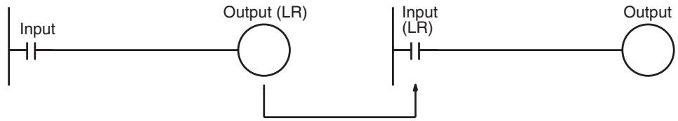
flowchart
graph LR
A["Input"] --> B((LR))
B --> C["Input (LR)"]
C --> D((Output))
The following conditions are taken as examples for calculating the I/O response times.
| Input ON delay: | 8 ms |
| Master cycle time: | 10 ms |
| Slave cycle time: | 15 ms |
| Output ON delay: | 10 ms |
| Direct output: | Not used. |
| Number of LR words: | 64 |
Note The input ON delay for DC Input Units can be set in the PC Setup.
Minimum I/O Response Time
The CQM1H responds most quickly under the following circumstances:
1,2,3... 1. The CQM1H receives an input signal just prior to the input refresh phase of the cycle.
2. The master to slave transmission begins immediately.
3. The slave executes communications servicing immediately after completion of communications.
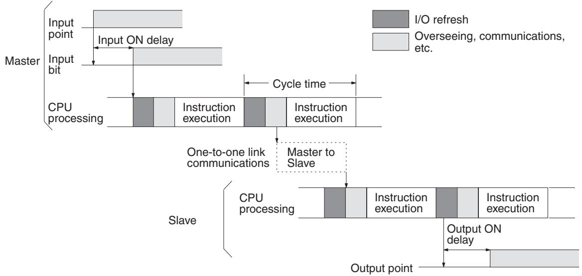
flowchart
graph TD
A["Master"] --> B["Input point"]
A --> C["Input bit"]
B --> D["Input ON delay"]
C --> E["CPU processing"]
D --> F["Instruction execution"]
E --> G["Instruction execution"]
F --> H["One-to-one link communications"]
G --> I["Master to Slave"]
H --> J["Output ON delay"]
I --> K["Output point"]
style A fill:#f9f,stroke:#333
style B fill:#ccf,stroke:#333
style C fill:#ccf,stroke:#333
style D fill:#cfc,stroke:#333
style E fill:#cfc,stroke:#333
style F fill:#fcc,stroke:#333
style G fill:#fcc,stroke:#333
style H fill:#cff,stroke:#333
style I fill:#cff,stroke:#333
style J fill:#ffc,stroke:#333
style K fill:#ffc,stroke:#333
The minimum I/O response time is as follows:
| Input ON delay: | 8 ms | |
| Master cycle time: | 10 ms | |
| Transmission time: | 39 ms | |
| Slave cycle time: | 15 ms | |
| + | Output ON delay: | 10 ms |
| Minimum I/O response time: | 82 ms |
Maximum I/O Response Time
The CQM1H takes the longest to respond under the following circumstances:
1,2,3...
- The CQM1H receives an input signal just after the input refresh phase of the cycle.
- The master to slave transmission does not begin on time.
- Communications are completed just after the slave executes communications servicing.
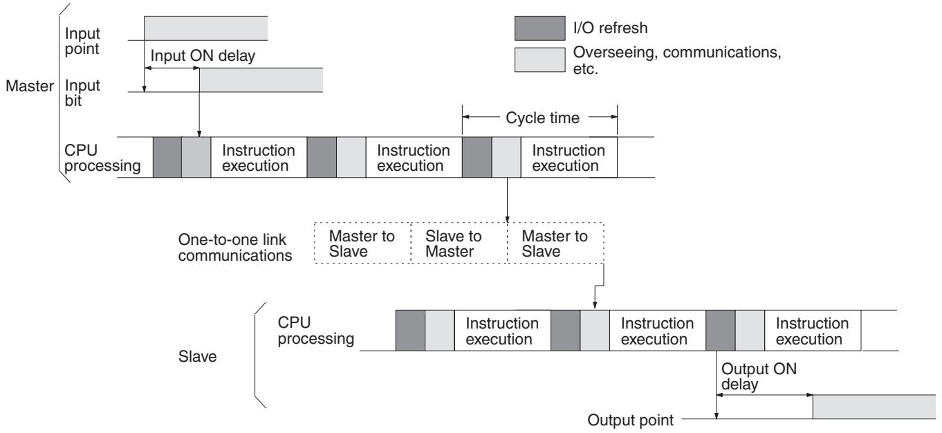
flowchart
graph TD
A["Input point"] --> B["Input ON delay"]
C["Input bit"] --> D["CPU processing"]
D --> E["Instruction execution"]
E --> F["Instruction execution"]
F --> G["Instruction execution"]
G --> H["One-to-one link communications"]
H --> I["Master to Slave"]
H --> J["Slave to Master"]
H --> K["Master to Slave"]
L["Output ON delay"] --> M["Output point"]
N["Master"] --> O["CPU processing"]
P["Slave"] --> Q["Instruction execution"]
R["Output"] --> S["Output point"]
The maximum I/O response time is as follows:
| Input ON delay: | 8 ms | |
| Master cycle time: | 10 ms × 2 | |
| Transmission time: | 39 ms × 3 | |
| Slave cycle time: | 15 ms × 2 | |
| + | Output ON delay: | 10 ms |
| Maximum I/O response time: | 185 ms |
7-3-5 Interrupt Processing Time
This section explains the processing times involved from the time an interrupt is executed until the interrupt processing routine is called, and from the time an interrupt processing routine is completed until returning to the original position. The explanation applies to the following three types of interrupts: input interrupts, interval timer interrupts, and high-speed counter interrupts.
Processing Time
The table below shows the times involved from the generation of an interrupt signal until the interrupt processing routine is called, and from when the interrupt processing routine is completed until returning to the original position.
| Item | Contents | Time |
| Interrupt input ON delay | This is the delay time from the time the interrupt input bit turns ON until the time that the interrupt is executed. This is unrelated to other interrupts. | 50 μs |
| ↓ (Interrupt condition realized.) (see note) | ||
| Standby until completion of interrupt-mask processing | This is the time during which interrupts are waiting until processing has been completed. This situation occurs when a mask processes is executed. It is explained below in more detail. | See below. |
| ↓ | ||
| Change-to-interrupt processing | This is the time it takes to change processing to an interrupt. | Input interrupts, internal timer interrupts, or high-speed counter interrupts: 30 μsInterrupts from Serial Communications Board: 55 μs |
| ↓ | ||
| Input refresh at time of interrupt | This is the time required for input refresh when input refresh is set to be executed at the time the interrupt processing routine is called. (Set in PC Setup, DM 6630 to DM 6638.) | 10 μs per word |
| ↓ (Interrupt processing routine executed) | ||
| Return | This is the time it takes, from execution of RET(93), to return to the processing that was interrupted. | 30 μs |
Note
- When high-speed counter 0 is used with a range comparison table, the timing of interrupt processing can be affected by the cycle time.
- When high-speed counters 1 and 2 for Pulse I/O Boards or Absolute Encoder Interface Boards are used with range comparison tables (with CQM1H-51/61 CPU Units), the timing of interrupt processing can be delayed up to 1 ms.
Mask Processing
Interrupts are masked during processing of the operations described below. Until the processing is completed, any interrupts will remain masked for the indicated times.
High-speed timers: The time shown below is required, depending on (a) the number of timers used with TIMH(15) and (b) the number of high-speed timers active at that time. (The number of high-speed timers is set in the PC Setup, DM 6629. The default setting is 16.)
$$ 0 \leq \text { Standby time } \leq 4 0 + 3 \times (a + b) \mu s $$
Up to 40 s can be required even when no high-speed timers are used.
Generation and clearing of non-fatal errors:
When a non-fatal error is generated and the error contents are registered at the CQM1H, or when an error is being cleared, interrupts will be masked for a maximum of 75 s until the processing has been completed.
Online editing: Interrupts will be masked for a maximum of 250 ms when online editing is executed during operation.
Pulse output based on SPED(64) may also be affected by interrupt processing, thus causing output timing to vary.
Example Calculation
This example shows the interrupt response time (i.e., the time from when the interrupt input turns ON until the start of the interrupt processing routine) when input interrupts are used under the conditions shown below.
Number of high-speed timers: 0 (No high-speed timers started)
Online edit: Not used
Input refresh at interrupt: No
Minimum Response Time
| Interrupt input ON delay: | 100 μs | |
| Interrupt mask standby time: | 0 μs | |
| + | Change-to-interrupt processing: | 30 μs |
| Minimum response time: | 130 μs |
Maximum Response Time
| Interrupt input ON delay: | 100 μs | |
| Interrupt mask standby time: | 40 μs | |
| + | Change-to-interrupt processing: | 30 μs |
| Minimum response time: | 170 μs |
In addition to the response time shown above, the time required for executing the interrupt processing routine itself and a return time of 30 s must also be accounted for when returning to the process that was interrupted.
Be sure to allow for interrupt processing time when using interrupts in the program.
Outputs from interrupt routines can be output immediately if direct output is used. Direct output will be used for both the main program and the interrupt routines, and cannot be set separately.
SECTION 8
Troubleshooting
This section describes how to diagnose and correct the hardware and software errors that can occur during operation.
8-1 Introduction.... 498
8-2 Programming Console Operation Errors.... 498
8-3 Programming Errors 499
8-4 User-defined Errors.... 500
8-5 Operating Errors 501
8-5-1 Non-fatal Errors 501
8-5-2 Fatal Errors 503
8-6 Error Log.... 504
8-7 Troubleshooting Flowcharts 505
8-1 Introduction
PC errors can be divided broadly into the following four categories:
1,2,3...
1. Program Input Errors
These errors occur when inputting a program or attempting an operation used to prepare the PC for operation.
2. Programming Errors
These errors will occur when the program is checked using the Program Check operation.
3. User-defined Errors
There are instructions that the user can use to define errors or messages. The instructions will be executed when a particular condition (defined by the user) has occurred during operation.
4. Operating Errors
These errors occur after program execution has been started.
a) Non-fatal Operating Errors
PC operation and program execution will continue after one or more of these errors have occurred.
b) Fatal Operating Errors
PC operation and program execution will stop and all outputs from the PC will be turned OFF when any of these errors have occurred.
The PC's indicators will indicate when a PC error has occurred and an error message or code will be displayed on the Programming Console or host computer if one is connected. The error code is also contained in SR 25300 to SR 25307.
For the most recent errors, both the type of error and time of occurrence will be recorded in the PC's error log area. Details are provided starting on page 504.
There are flags and other information provided in the SR and AR areas that can be used in troubleshooting. Refer to SECTION 3 Memory Areas for lists of these.
Note In addition to the errors described above, communications errors can occur when the PC is part of a Host Link System. Refer to SECTION 6 Host Link Commands for details.
8-2 Programming Console Operation Errors
The following error messages may appear when performing operations on the Programming Console. Correct the error as indicated and continue with the operation. Refer to the Ladder Support Software Operation Manual, SYSMAC Support Software Operation Manual: C-series PCs, or Data Access Console Operation Manual for errors that may appear when operating the SSS or a Data Access Console.
| Message | Meaning and appropriate response |
| REPL ROM | An attempt was made to write to write-protected memory. Set the write-protect switch (pin 1 of the CPU Unit's DIP switch) to OFF. |
| PROG OVER | The instruction at the last address in memory is not NOP(00). Erase all unnecessary instructions at the end of the program. |
| ADDR OVER | An address was set that is larger than the highest memory address in Program Memory. Input a smaller address. |
| SET DATA ERR | FALS 00 has been input, and “00” cannot be input. Reinput the data. |
| I/O NO. ERR | A data area address has been designated that exceeds the limit of the data area, e.g., an address is too large. Confirm the requirements for the instruction and re-enter the address. |
8-3 Programming Errors
These errors in program syntax will be detected when the program is checked using the Program Check operation.
Three levels of program checking are available. The desired level must be designated to indicate the type of errors that are to be detected. The following table provides the error types, displays, and explanations of all syntax errors. Check level 0 checks for type A, B, and C errors; check level 1, for type A and B errors; and check level 2, for type A errors only.
Level A Errors
| Message | Meaning and appropriate response |
| ????? | The program has been damaged, creating a non-existent function code. Re-enter the program. |
| CIRCUIT ERR | The number of logic blocks and logic block instructions does not agree, i.e., either LD or LD NOT has been used to start a logic block whose execution condition has not been used by another instruction, or a logic block instruction has been used that does not have the required number of logic blocks. Check your program. |
| OPERAND ERR | A constant entered for the instruction is not within defined values. Change the constant so that it lies within the proper range. |
| NO END INSTR | There is no END(01) in the program. Write END(01) at the final address in the program. |
| LOCN ERR | An instruction is in the wrong place in the program. Check instruction requirements and correct the program. |
| JME UNDEFD | A JME(05) instruction is missing for a JMP(04) instruction. Correct the jump number or insert the proper JME(05) instruction. |
| DUPL | The same jump number or subroutine number has been used twice. Correct the program so that the same number is only used once for each. |
| SBN UNDEFD | The SBS(91) instruction has been programmed for a subroutine number that does not exist. Correct the subroutine number or program the required subroutine. |
| STEP ERR | STEP(08) with a section number and STEP(08) without a section number have been used incorrectly. Check STEP(08) programming requirements and correct the program. |
Level B Errors
| Message | Meaning and appropriate response |
| IL-ILC ERR | IL(02) and ILC(03) are not used in pairs. Correct the program so that each IL(02) has a unique ILC(03). Although this error message will appear if more than one IL(02) is used with the same ILC(03), the program will be executed as written. Make sure your program is written as desired before proceeding. |
| JMP-JME ERR | JMP(04) and JME(05) are not used in pairs. Make sure your program is written as desired before proceeding. |
| SBN-RET ERR | If the displayed address is that of SBN(92), two different subroutines have been defined with the same subroutine number. Change one of the subroutine numbers or delete one of the subroutines. If the displayed address is that of RET(93), RET(93) has not been used properly. Check requirements for RET(93) and correct the program. |
Level C Errors
| Message | Meaning and appropriate response |
| COIL DUPL | The same bit is being controlled (i.e., turned ON and/or OFF) by more than one instruction (e.g., OUT, OUT NOT, DIFU(13), DIFD(14), KEEP(11), SFT(10)). Although this is allowed for certain instructions, check instruction requirements to confirm that the program is correct or rewrite the program so that each bit is controlled by only one instruction. |
| JMP UNDEFD | JME(05) has been used with no JMP(04) with the same jump number. Add a JMP(04) with the same number or delete the JME(05) that is not being used. |
| SBS UNDEFD | A subroutine exists that is not called by SBS(91). Program a subroutine call in the proper place, or delete the subroutine if it is not required. |
Caution
Expansion instructions (those assigned to function codes 17, 18, 19, 47, 48, 60 to 69, 87, 88, and 89) are not subject to program checks. Program checks also do not cover DM 3070 to DM 6143 for PCs that do not support this part of the DM area (e.g., CQM1H-CPU11 and CQM1H-CPU21). Data will not be written even if these areas are specified and data read from these areas will always be undefined.
8-4 User-defined Errors
MESSAGE - MSG(46)
There are four instructions that the user can use to define errors or messages. These instructions can be used to generate warnings (non-fatal errors where the ERR/ALM flashes) or errors (fatal errors where the ERR/ALM lights), and to display messages at the Programming Console.
MSG(46) is used to display a message on the Programming Console. The message, which can be up to 16 characters long, is displayed when the instruction's execution condition is ON. Refer to page 381 for details.
FAILURE ALARM – FAL(06)
FAL(06) is an instruction that causes a non-fatal error. Refer to page 230 for details. The following will occur when an FAL(06) instruction is executed:
1,2,3...
- The ERR/ALM indicator on the CPU Unit will flash. PC operation will continue.
- The instruction's 2-digit BCD FAL number (01 to 99) will be written to SR 25300 to SR 25307.
- The FAL number will be recorded in the PC's error log area. The time of occurrence will also be recorded if a Memory Cassette with a clock (RTC) is used.
The FAL numbers can be set arbitrarily to indicate particular conditions. The same number cannot be used as both an FAL number and an FALS number.
To clear an FAL error, correct the cause of the error, execute FAL 00, and then clear the error using the Programming Console. Refer to page 230 for details.
SEVERE FAILURE ALARM – FALS(07)
FALS(07) is an instruction that causes a fatal error. Refer to page 230 for details. The following will occur when an FALS(07) instruction is executed:
1,2,3...
- Program execution will be stopped and outputs will be turned OFF.
- The ERR/ALM indicator on the CPU Unit will be lit.
-
The instruction's 2-digit BCD FALS number (01 to 99) will be written to SR 25300 to SR 25307.
-
The FALS number will be recorded in the PC's error log area. The time of occurrence will also be recorded if a Memory Cassette with a clock (RTC) is used.
The FALS numbers can be set arbitrarily to indicate particular conditions. The same number cannot be used as both an FAL number and an FALS number.
To clear an FALS error, switch the PC to PROGRAM Mode, correct the cause of the error, and then clear the error using the Programming Console.
FAILURE POINT DETECT - FPD(—)
Non-fatal errors and error messages can also be generated using FPD(—). Refer to page 387 for details.
8-5 Operating Errors
There are two kinds of operating errors, non-fatal and fatal. PC operation will continue after a non-fatal error occurs, but operation will be stopped if a fatal error occurs.
Caution
Investigate all errors, whether fatal or not. Remove the cause of the error as soon as possible and restart the PC. Refer to the CQM1H Operation Manual for hardware information and Programming Console operations related to errors.
8-5-1 Non-fatal Errors
PC operation and program execution will continue after one or more of these errors have occurred. Although PC operation will continue, the cause of the error should be corrected and the error cleared as soon as possible.
When one of these errors occurs, the POWER and RUN indicators will remain lit and the ERR/ALM indicator will flash.
Caution
Although PC operation continues even when non-fatal errors are generated, investigate the cause of errors and take the appropriate action as soon as possible. After removing the cause of the error, either turn the PC OFF and ON again, or clear the error from a Programming Console. Refer to the CQM1H Operation Manual for Programming Console procedures.
Note ** is 01 to 99, 9D, 9C, or 9B.
| Message | FAL No. | Meaning and appropriate response |
| SYS FAIL FAL**(see note) | 01 to 99 | An FAL(06) instruction has been executed in the program. Check the FAL number to determine conditions that would cause execution, correct the cause, and clear the error. |
| 9D | An error has occurred during data transmission between the CPU Unit and Memory Cassette. Check the status of flags AR 1412 to AR 1415, and correct as directed.AR 1412 ON: Switch to PROGRAM Mode, clear the error, and transfer again.AR 1413 ON: The transfer destination is write-protected.If the PC is the destination, turn OFF the power to the PC, be sure that pin 1 of the CPU Unit's DIP switch is OFF, clear the error, and transfer again.If an EEPROM Memory Cassette is the destination, check whether the power supply is ON, clear the error, and transfer again.If an EPROM Memory Cassette is the destination, change to a writable Memory Cassette.AR 1414 ON: The destination has insufficient capacity. Check the source's program size in AR 15 and consider using a different CPU Unit or Memory Cassette.AR 1415 ON: There is no program in the Memory Cassette or the program contains errors. Check the Memory Cassette. | |
| SYS FAIL FAL **(see note) | 9C | Check the contents (two digits BCD) of AR 0400 to AR 0407 (error codes for Inner Board inserted in slot 1) and correct as directed.01, 02 Hex: An error has occurred in the hardware. Turn the power OFF, and then power up again. If the error persists, replace the Inner Board.03 Hex: The PC Setup (DM 6650 to DM 6559, DM 6613, DM 6614, DM 6602, DM 6603, DM 6640, DM 6641) settings are incorrect. Correct the settings.10 Hex: An error has occurred in the Serial Communications Board. Check flags and status information in memory for the Serial Communications Board and correct the error accordingly.An error has occurred in the Inner Board inserted in slot 1 or slot 2.Check the contents (two digits BCD) of AR 0408 to AR 0415 (error codes for Inner Board inserted in slot 2) and correct as directed.01, 02 Hex: An error has occurred in the hardware. Turn the power OFF, and then power up again. If the error persists, replace the Inner Board.03 Hex: The PC Setup (DM 6611, DM 6612, DM 6643, DM 6644) settings are incorrect. Correct the settings.04 Hex: CQM1H operation was interrupted during pulse output (when CQM1H-PLB21 is mounted). Check to see whether the device receiving the pulse output was affected. |
| 9B | An error has been detected in the PC Setup. Check flags AR 2400 to AR 2402, and correct as directed.AR 2400 ON: An incorrect setting was detected in the PC Setup (DM 6600 to DM 6614) when power was turned ON. Correct the settings in PROGRAM Mode and turn on the power again.AR 2401 ON: An incorrect setting was detected in the PC Setup (DM 6615 to DM 6644) when switching to RUN Mode. Correct the settings in PROGRAM Mode and switch to RUN Mode again.AR 2402 ON: An incorrect setting was detected in the PC Setup (DM 6645 to DM 6655) during operation. Correct the settings and clear the error. | |
| SCAN TIME OVER | F8 | Watchdog timer has exceeded 100 ms. (SR 25309 will be ON.)This indicates that the program cycle time is longer than recommended. Reduce cycle time if possible. |
| BATT LOW | F7 | Backup battery is missing or its voltage has dropped. (SR 25308 will be ON.)Check the battery and replace if necessary. Check the PC Setup (DM 6655) to see whether a low battery will be detected. |
| SIOU_ERR | D0 | An error has occurred during data transfer between the CPU Unit and the Controller Link Unit, or in the Controller Link Unit itself. (SR 25413 and AR 0011 will be ON.)Turn the power OFF, and then ON again. If the error persists, replace the Controller Link Unit. |
Communication Errors
If an error occurs in communications through the peripheral port or built-in RS-232C port, the corresponding indicator (PRPHL or COMM) will stop flashing. Check the connecting cables as well as the programs in the PC and host computer.
Reset the communications ports with the Port Reset Bits, SR 25208 and SR 25209.
Output Inhibit
When the OUT INH indicator is lit, the Output OFF Bit (SR 25215) is ON and all outputs from the CPU Unit will be turned OFF. If it is not necessary to have all outputs OFF, turn OFF SR 25215.
8-5-2 Fatal Errors
PC operation and program execution will stop and all outputs from the PC will be turned OFF when any of these errors have occurred.
All CPU Unit indicators will be OFF for the power interruption error. For all other fatal operating errors, the POWER and ERR/ALM indicators will be lit. The RUN indicator will be OFF.
Caution
Investigate the cause of errors and take the appropriate action as soon as possible. After removing the cause of the error, either turn the PC OFF and ON again, or perform error clearing operations. Refer to the CQM1H Operation Manual for Programming Console procedures.
| Message | FALS No. | Meaning and appropriate response |
| Power interruption (no message) | None | Power has been interrupted for at least 10 ms. Check power supply voltage and power lines. Try to power-up again. |
| MEMORY ERR | F1 | AR 1611 ON: A checksum error has occurred in the PC Setup (DM 6600 to DM 6655). Initialize all of the PC Setup and reinput. |
| AR 1612 ON: A checksum error has occurred in the program, indicating an incorrect instruction. Check the program and correct any errors detected. | ||
| AR 1613 ON: A checksum error has occurred in an expansion instruction's data. Initialize all of the expansion instruction settings and reinput. | ||
| AR 1614 ON: Memory Cassette was installed or removed with the power ON. Turn the power OFF, install the Memory Cassette, and turn the power on again. | ||
| AR 1615 ON: The Memory Cassette contents could not be read at start-up. Check flags AR 1412 to AR 1415 to determine the problem, correct it, and turn ON the power again. | ||
| NO END INST | F0 | END(01) is not written anywhere in program. Write END(01) at the final address of the program. |
| I/O BUS ERR | C0 | An error has occurred during data transfer between the CPU Unit and an I/O Unit.An I/O Unit or the End Cover is not connected properly.An Inner Board was connected or removed during communications.The End Cover is not connected correctly to the CPU Block or Expansion I/O Block.The power supply voltage supplied to the Expansion I/O Block is not sufficient.More than one I/O Control Unit or I/O Interface Unit is mounted.Determine the location of the problem using the error code stored in AR 2400 to AR 2415. Turn OFF the power and check the following according to the error code.Error code: 00 to 15 BCDCheck the mounting of the Unit allocated input words IR 000 to IR 015.Error code: 80 to 95 BCDCheck the mounting of the Unit allocated output words IR 100 to IR 115.Error code: F0 HexCheck the mounting of the Inner Board in slot 1.Error code: F1 HexCheck the mounting of the Inner Board in slot 2.Error code: FF HexCheck the mounting of the End Cover on the CPU Block or Expansion I/O Block.Check the Expansion I/O Cable length. The cable must be 0.7 m max.Check the number of Units and the current consumption on the CPU Block and Expansion I/O Block to see if the maximum number of Units or the power supply capacity has been exceeded. If necessary, reconfigure the system to enable adequate power supply. |
| I/O UNIT OVER | E1 | The number of I/O words on the installed I/O Units exceeds the maximum. Turn OFF the power, rearrange the system to reduce the number of I/O words, and turn ON the power again. |
| SYS FAIL FALS**(see note) | 01 to 99 | An FALS(07) instruction has been executed in the program. Check the FALS number to determine the conditions that would cause execution, correct the cause, and clear the error. |
| 9F | The cycle time has exceeded the FALS 9F Cycle Time Monitoring Time (DM 6618). Check the cycle time and adjust the Cycle Time Monitoring Time if necessary. |
Note ** is 01 to 99 or 9F.
8-6 Error Log
The error log registers the error code of any fatal or non-fatal error that occurs in the PC. The date and time at which the error occurred are registered along with the error code. Refer to page 501 for error codes.
Error Log Area
The error log is stored in DM 6569 through DM 6599 as shown below.
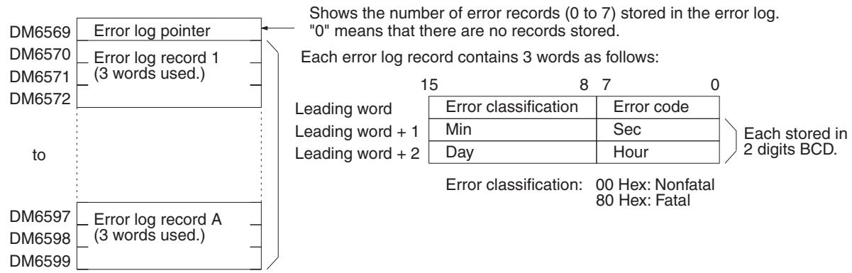
Error Log Storage Methods
Error records will be stored even if pin 1 on the DIP switch on the CPU Unit is turned ON to protect DM 6144 to DM 6655.
For details about error codes refer to 8-5 Operating Errors.
If the settings in PC Setup (DM 6655, bits 00 to 03) are set to disable saving records to the error history (2 to F Hex), DM 6569 to DM 6599 can be used as general-purpose read-only DM words.
The error log storage method is set in the PC Setup (DM 6655, bits 00 to 03). Set any of the following methods.
- 0 Hex: You can store the most recent 10 error log records and discard older records. This is achieved by shifting the records as shown below so that the oldest record (record 0) is lost whenever a new record is generated.
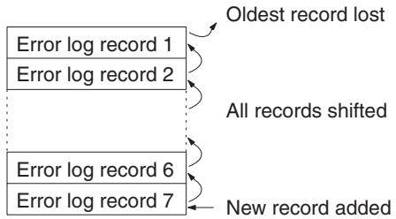
flowchart
graph TD
A["Error log record 1"] --> B["All records shifted"]
C["Error log record 2"] --> B
D["..."] --> E["New record added"]
F["Error log record 6"] --> E
G["Error log record 7"] --> E
B --> H["Oldest record lost"]
E --> I["New record added"]
- 1 Hex: You can store only the first 10 error log records, and ignore any subsequent errors beyond those 10.
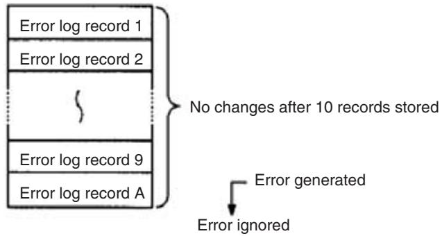
flowchart
graph TD
A["Error log record 1"] --> B{No changes after 10 records stored}
C["Error log record 2"] --> B
D["..."] --> B
E["Error log record 9"] --> F{Error generated}
G["Error log record A"] --> F
F --> H["Error ignored"]
- 2 to F Hex: You can disable the log so that no records are stored.
The default setting is the first method. Refer to Error Log Settings on page 17 for details on the PC Setup for the error log.
Note
- If a Memory Cassette with a clock (RTC) is not used, the date and time of error occurrence will be "0000."
- Error will be recorded in the error log even if DM 6144 to DM 6655 are write-protected by turning ON pin 1 on the DIP switch on the front side of the CPU Unit.
Clearing the Error Log
To clear the entire error log, turn ON SR 25214 from a Programming Device or using an instruction. (After the error log has been cleared, SR 25214 will turn OFF automatically.)
8-7 Troubleshooting Flowcharts
Use the following flowcharts to troubleshoot errors that occur during operation.
Main Check
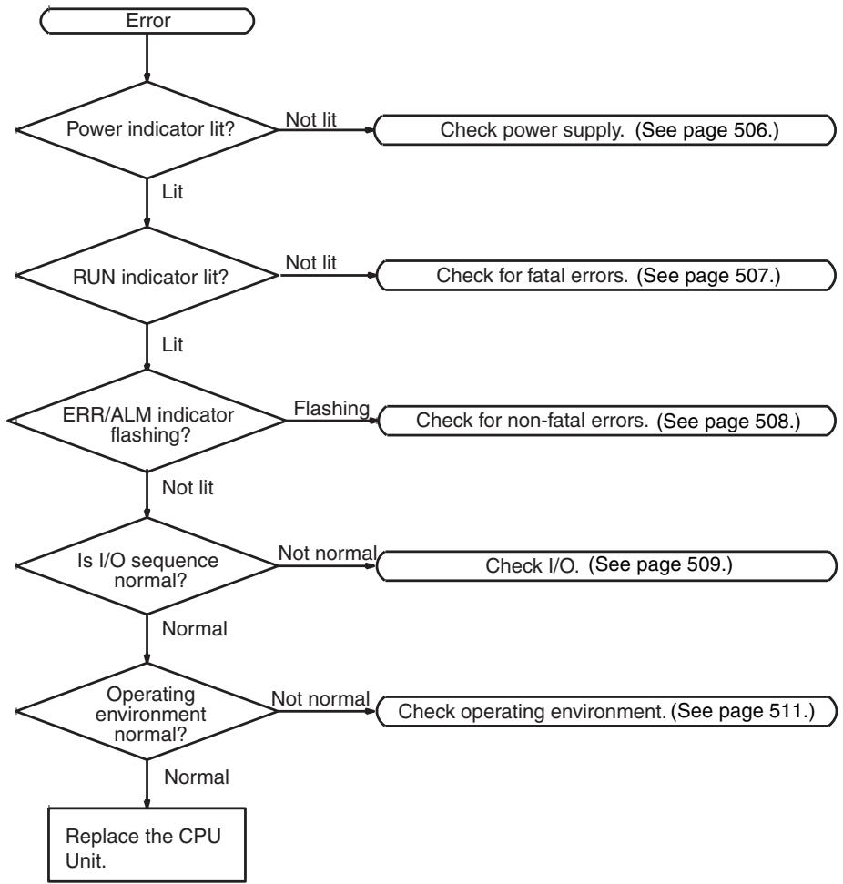
flowchart
graph TD
A["Error"] --> B{Power indicator lit?}
B -->|Not lit| C["Check power supply. (See page 506.)"]
B -->|Lit| D{RUN indicator lit?}
D -->|Not lit| E["Check for fatal errors. (See page 507.)"]
D -->|Lit| F{ERR/ALM indicator flashing?}
F -->|Flashing| G["Check for non-fatal errors. (See page 508.)"]
F -->|Not lit| H{Is I/O sequence normal?}
H -->|Not normal| I["Check I/O. (See page 509.)"]
H -->|Normal| J{Operating environment normal?}
J -->|Not normal| K["Check operating environment. (See page 511.)"]
J -->|Normal| L["Replace the CPU Unit."]
Note Always turn OFF the power to the PC before replacing Units, batteries, wiring, or cables.
Power Supply Check
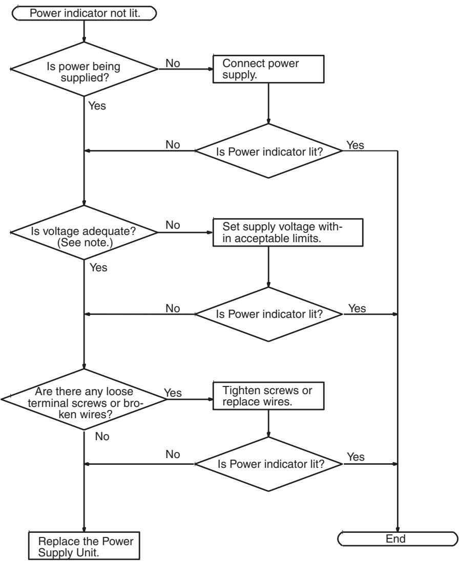
flowchart
graph TD
A["Power indicator not lit."] --> B{Is power being supplied?}
B -->|No| C["Connect power supply."]
B -->|Yes| D{Is voltage adequate? (See note.)}
C --> D
D -->|No| E["Set supply voltage within acceptable limits."]
D -->|Yes| F{Is Power indicator lit?}
E --> F
F -->|No| G{Are there any loose terminal screws or broken wires?}
F -->|Yes| H["Tighten screws or replace wires."]
G --> I{Is Power indicator lit?}
H --> I
I -->|No| J["Replace the Power Supply Unit."]
I -->|Yes| K["End"]
Note Refer to CQM1H Operation Manual for the allowable voltage ranges for the CQM1H.
Fatal Error Check
The following flowchart can be used to troubleshoot fatal errors that occur while the Power indicator is lit.
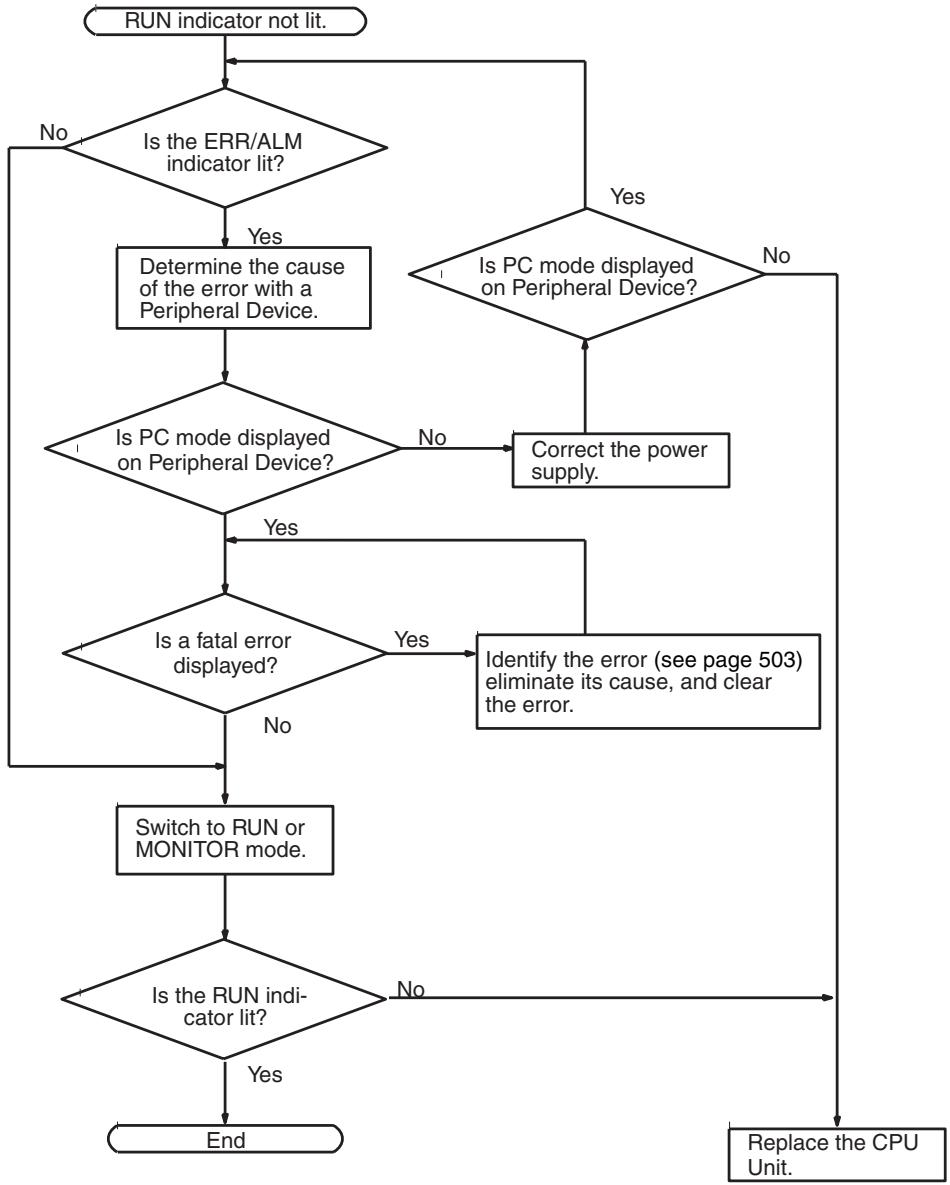
flowchart
graph TD
A["RUN indicator not lit."] --> B{Is the ERR/ALM indicator lit?}
B -->|No| A
B -->|Yes| C["Determine the cause of the error with a Peripheral Device."]
C --> D{Is PC mode displayed on Peripheral Device?}
D -->|No| E["Correct the power supply."]
D -->|Yes| F{Is a fatal error displayed?}
F -->|No| G["Switch to RUN or MONITOR mode."]
F -->|Yes| H["Identify the error (see page 503) eliminate its cause, and clear the error."]
H --> I{Is the RUN indicator lit?}
I -->|No| J["Replace the CPU Unit."]
I -->|Yes| K["End"]
Non-fatal Error Check
Although the PC will continue operating during non-fatal errors, the cause of the error should be determined and removed as quickly as possible to ensure proper operation. It may to necessary to stop PC operation to remove certain non-fatal errors.
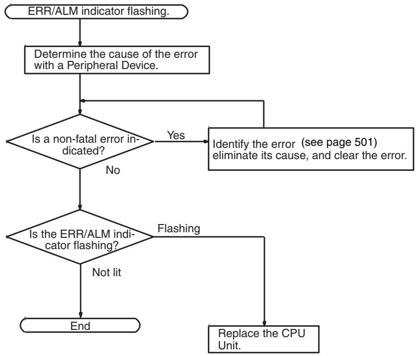
flowchart
graph TD
A["ERR/ALM indicator flashing."] --> B["Determine the cause of the error with a Peripheral Device."]
B --> C{Is a non-fatal error indicated?}
C -->|Yes| D["Identify the error (see page 501) eliminate its cause, and clear the error."]
C -->|No| E{Is the ERR/ALM indicator flashing?}
E -->|Yes| F["Replace the CPU Unit."]
E -->|No| G["End"]
I/O Check
The I/O check flowchart is based on the following ladder diagram section.

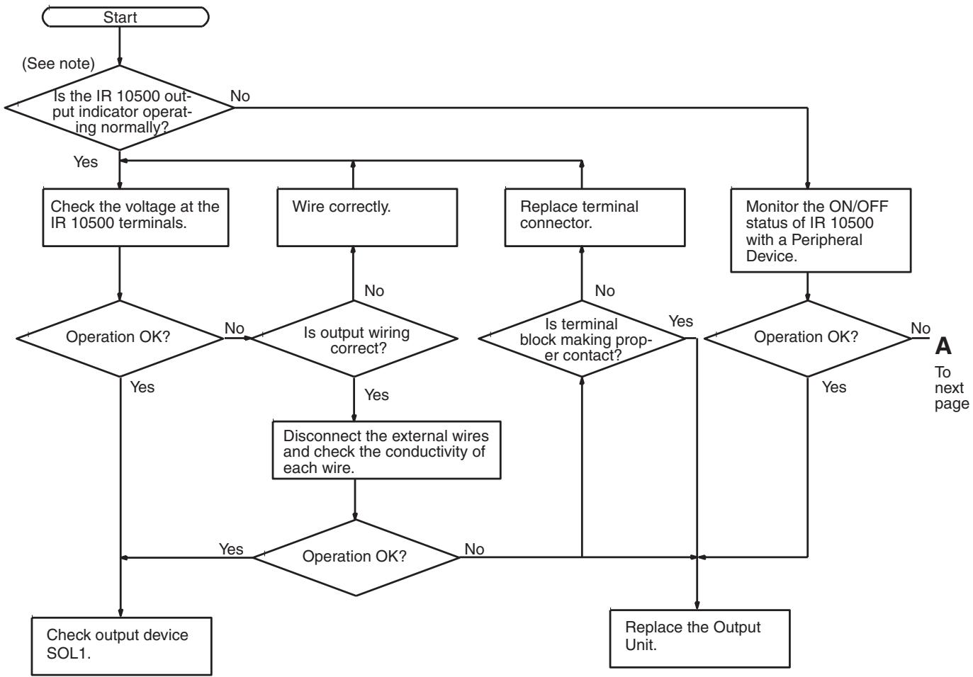
flowchart
graph TD
A["Start"] --> B{(See note)}
B -->|Yes| C["Check the voltage at the IR 10500 terminals."]
B -->|No| D{Is the IR 10500 output indicator operating normally?}
C --> E{Operation OK?}
D --> F{Is output wiring correct?}
F -->|Yes| G["Disconnect the external wires and check the conductivity of each wire."]
F -->|No| H{Is terminal block making proper contact?}
H -->|Yes| I{Operation OK?}
H -->|No| J["Replace the ON/OFF status of IR 10500 with a Peripheral Device."]
I --> K{Operation OK?}
I --> L["Replace the Output Unit."]
J --> M{Operation OK?}
M --> N["Check output device SOL1."]
D --> O{Wire correctly.}
O --> P["No"]
P --> Q{Is output wiring correct?}
Q -->|Yes| R["Disconnect the external wires and check the conductivity of each wire."]
Q -->|No| S{Is terminal block making proper contact?}
S -->|Yes| T["Replace terminal connector."]
S -->|No| U{Is terminal block making proper contact?}
U -->|Yes| V["Monitor the ON/OFF status of IR 10500 with a Peripheral Device."]
U -->|No| W["To next page"]
V --> X{Operation OK?}
X --> Y["No"]
Y --> Z["Replace the Output Unit."]
The error may be due to a blown fuse or output transistor malfunction.
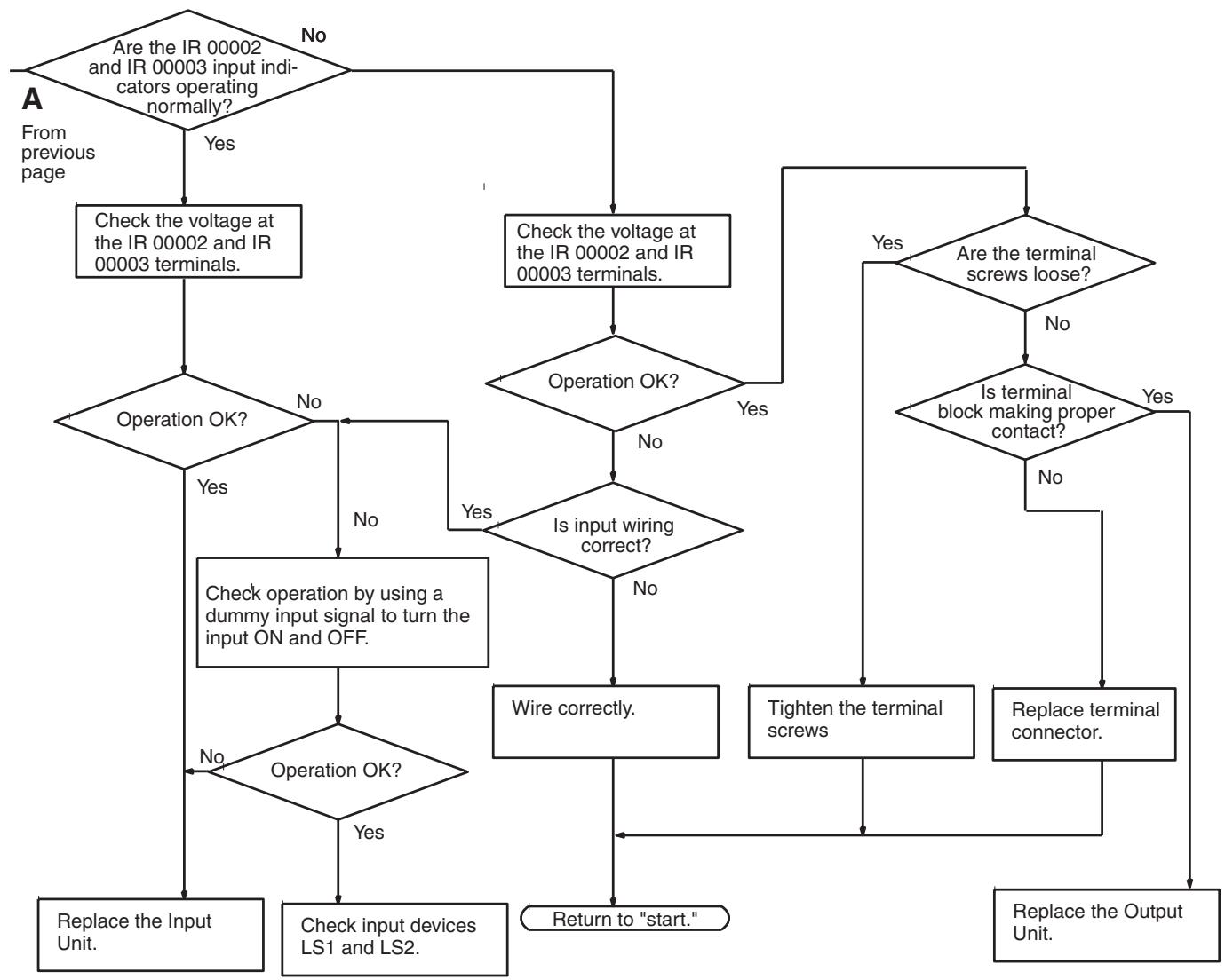
flowchart
graph TD
A{Are the IR 00002 and IR 00003 input indicators operating normally?}
B["Check the voltage at the IR 00002 and IR 00003 terminals."] --> C{Operation OK?}
C -->|No| D["Check operation by using a dummy input signal to turn the input ON and OFF."]
C -->|Yes| E["Check input devices LS1 and LS2."]
D --> F{Operation OK?}
F -->|No| G["Replace the Input Unit."]
F -->|Yes| H["Check operation OR"]
H --> I{Is input wiring correct?}
I -->|No| J["Wire correctly."]
I -->|Yes| K{Tile with 'Is terminal block making proper contact?'}
K -->|No| L["Replace terminal connector."]
K -->|Yes| M{Are the terminal screws loose?}
M -->|No| N["Tighten the terminal screws"]
M -->|Yes| O{Are the terminal screws loose?}
O -->|No| P["Replace the Output Unit."]
O -->|Yes| Q["End"]
Q --> R["Return to "start.""]
B --> S["Check the voltage at the IR 00002 and IR 00003 terminals."]
S --> T{Operation OK?}
T -->|No| U["Check operation OR"]
T -->|Yes| V["End"]
Environmental Conditions Check
flowchart
graph TD
A["Environmental conditions check"] --> B{Is the ambient temperature below 55°C?}
B -->|No| C["Consider using a fan or cooler."]
B -->|Yes| D{Is the ambient temperature above 0°C?}
D -->|No| E["Consider using a heater."]
D -->|Yes| F{Is the ambient humidity between 10% and 90%?}
F -->|No| G["Consider using an air conditioner."]
F -->|Yes| H{Is noise being controlled?}
H -->|No| I["Install surge protectors or other noise-reducing equipment at noise sources."]
H -->|Yes| J{Is the installation environment okay?}
J -->|No| K["Consider constructing an instrument panel or cabinet."]
J -->|Yes| L["End."]
Appendix A
Programming Instructions
A PC instruction is input either by pressing the corresponding Programming Console key(s) (e.g., LD, AND, OR, NOT) or by using function codes. To input an instruction with its function code, press FUN, the function code, and then WRITE. Refer to the pages listed programming and instruction details.
| Code | Mnemonic | Name | Function | Page |
| — | AND | AND | Logically ANDs status of designated bit with execution condition. | 222 |
| — | AND LD | AND LOAD | Logically ANDs results of preceding blocks. | 223 |
| — | AND NOT | AND NOT | Logically ANDs inverse of designated bit with execution condition. | 222 |
| — | CNT | COUNTER | A decrementing counter. | 235 |
| — | LD | LOAD | Used to start instruction line with the status of the designated bit or to define a logic block for use with AND LD and OR LD. | 222 |
| — | LD NOT | LOAD NOT | Used to start instruction line with inverse of designated bit. | 222 |
| — | OR | OR | Logically ORs status of designated bit with execution condition. | 222 |
| — | OR LD | OR LOAD | Logically ORs results of preceding blocks. | 223 |
| — | OR NOT | OR NOT | Logically ORs inverse of designated bit with execution condition. | 222 |
| — | OUT | OUTPUT | Turns ON operand bit for ON execution condition; turns OFF operand bit for OFF execution condition. | 224 |
| — | OUT NOT | OUTPUT NOT | Turns operand bit OFF for ON execution condition; turns oper- and bit ON for OFF execution condition (i.e., inverts opera-tion). | 224 |
| — | RSET | RESET | Turns the operand bit OFF when the execution condition is ON, and does not affect the status of the operand bit when the execution condition is OFF. | 224 |
| — | SET | SET | Turns the operand bit ON when the execution condition is ON, and does not affect the status of the operand bit when the exec-cution condition is OFF. | 224 |
| — | TIM | TIMER | ON-delay (decrementing) timer operation. | 234 |
| 00 | NOP | NO OPERATION | Nothing is executed and program moves to next instruction. | 227 |
| 01 | END | END | Required at the end of the program. | 227 |
| 02 | IL | INTERLOCK | If interlock condition is OFF, all outputs are turned OFF and all timer PVs reset between this IL(02) and the next ILC(03). Other instructions are treated as NOP; counter PVs are main-tained. | 227 |
| 03 | ILC | INTERLOCK CLEAR | 227 | |
| 04 | JMP | JUMP | If jump condition is OFF, all instructions between JMP(04) and the corresponding JME(05) are ignored. | 229 |
| 05 | JME | JUMP END | 229 | |
| 06 | (@)FAL | FAILURE ALARM AND RESET | Generates a non-fatal error and outputs the designated FAL number to the Programming Console. | 230 |
| 07 | FALS | SEVERE FAILURE ALARM | Generates a fatal error and outputs the designated FALS num-ber to the Programming Console. | 230 |
| 08 | STEP | STEP DEFINE | When used with a control bit, defines the start of a new step and resets the previous step. When used without N, defines the end of step execution. | 231 |
| 09 | SNXT | STEP START | Used with a control bit to indicate the end of the step, reset the step, and start the next step. | 231 |
| 10 | SFT | SHIFT REGISTER | Creates a bit shift register. | 261 |
| 11 | KEEP | KEEP | Defines a bit as a latch controlled by set and reset inputs. | 225 |
| 12 | CNTR | REVERSIBLE COUNTER | Increases or decreases PV by one whenever the increment input or decrement input signals, respectively, go from OFF to ON. | 237 |
| 13 | DIFU | DIFFERENTIATE UP | Turns ON the designated bit for one cycle on the rising edge of the input signal. | 226 |
| 14 | DIFD | DIFFERENTIATE DOWN | Turns ON the bit for one cycle on the trailing edge. | 226 |
| 15 | TIMH | HIGH-SPEED TIMER | A high-speed, ON-delay (decrementing) timer. | 238 |
| 16 | (@)WSFT | WORD SHIFT | Shifts data between starting and ending words in word units, writing zeros into starting word. | 262 |
| 17 to 19 | For expansion instructions. | 213 | ||
| 20 | CMP | COMPARE | Compares the contents of two words and outputs result to GR, EQ, and LE Flags. | 280 |
| 21 | (@)MOV | MOVE | Copies source data (word or constant) to destination word. | 269 |
| 22 | (@)MVN | MOVE NOT | Inverts source data (word or constant) and then copies it to destination word. | 270 |
| 23 | (@)BIN | BCD TO BINARY | Converts four-digit, BCD data in source word into 16-bit binary data, and outputs converted data to result word. | 291 |
| 24 | (@)BCD | BINARY TO BCD | Converts binary data in source word into BCD, and outputs converted data to result word. | 292 |
| 25 | (@)ASL | ARITHMETIC SHIFT LEFT | Shifts each bit in single word of data one bit to left, with CY. | 263 |
| 26 | (@)ASR | ARITHMETIC SHIFT RIGHT | Shifts each bit in single word of data one bit to right, with CY. | 263 |
| 27 | (@)ROL | ROTATE LEFT | Rotates bits in single word of data one bit to left, with CY. | 264 |
| 28 | (@)ROR | ROTATE RIGHT | Rotates bits in single word of data one bit to right, with CY. | 264 |
| 29 | (@)COM | COMPLEMENT | Inverts bit status of one word of data. | 372 |
| 30 | (@)ADD | BCD ADD | Adds two four-digit BCD values and content of CY, and outputs result to specified result word. | 317 |
| 31 | (@)SUB | BCD SUBTRACT | Subtracts a four-digit BCD value and CY from another four-digit BCD value and outputs result to the result word. | 318 |
| 32 | (@)MUL | BCD MULTIPLY | Multiplies two four-digit BCD values and outputs result to specified result words. | 320 |
| 33 | (@)DIV | BCD DIVIDE | Divides four-digit BCD dividend by four-digit BCD divisor and outputs result to specified result words. | 321 |
| 34 | (@)ANDW | LOGICAL AND | Logically ANDs two 16-bit input words and sets corresponding bit in result word if corresponding bits in input words are both ON. | 373 |
| 35 | (@)ORW | LOGICAL OR | Logically ORs two 16-bit input words and sets corresponding bit in result word if one or both of corresponding bits in input data are ON. | 374 |
| 36 | (@)XORW | EXCLUSIVE OR | Exclusively ORs two 16-bit input words and sets bit in result word when corresponding bits in input words differ in status. | 374 |
| 37 | (@)XNRW | EXCLUSIVE NOR | Exclusively NORs two 16-bit input words and sets bit in result word when corresponding bits in input words are same in status. | 375 |
| 38 | (@)INC | BCD INCREMENT | Increments four-digit BCD word by one. | 376 |
| 39 | (@)DEC | BCD DECREMENT | Decrements four-digit BCD word by one. | 376 |
| 40 | (@)STC | SET CARRY | Sets carry flag (i.e., turns CY ON). | 317 |
| 41 | (@)CLC | CLEAR CARRY | Clears carry flag (i.e., turns CY OFF). | 317 |
| 45 | TRSM | TRACE MEMORY SAMPLE | Initiates data tracing. | 379 |
| 46 | (@)MSG | MESSAGE | Displays a 16-character message on the Programming Console display. | 381 |
| 47 & 48 | For expansion instructions. | 213 | ||
| 50 | (@)ADB | BINARY ADD | Adds two four-digit hexadecimal values and content of CY, and outputs result to specified result word. | 328 |
| 51 | (@)SBB | BINARY SUBTRACT | Subtracts a four-digit hexadecimal value and CY from another four-digit hexadecimal value and outputs result to the result word. | 329 |
| 52 | (@)MLB | BINARY MULTIPLY | Multiplies two four-digit hexadecimal values and outputs result to specified result words. | 330 |
| 53 | (@)DVB | BINARY DIVIDE | Divides four-digit hexadecimal dividend by four-digit hexadecimal divisor and outputs result to specified result words. | 331 |
| 54 | (@)ADDL | DOUBLE BCD ADD | Adds two eight-digit values (2 words each) and content of CY, and outputs result to specified result words. | 323 |
| 55 | (@)SUBL | DOUBLE BCD SUB-TRACT | Subtracts an eight-digit BCD value and CY from another eight-digit BCD value and outputs result to the result words. | 324 |
| 56 | (@)MULL | DOUBLE BCD MULTI-PLY | Multiplies two eight-digit BCD values and outputs result to specified result words. | 325 |
| 57 | (@)DIVL | DOUBLE BCD DIVIDE | Divides eight-digit BCD dividend by eight-digit BCD divisor and outputs result to specified result words. | 326 |
| 58 | (@)BINL | DOUBLE BCD TO DOUBLE BINARY | Converts BCD value in two consecutive source words into binary and outputs converted data to two consecutive result words. | 293 |
| 59 | (@)BCDL | DOUBLE BINARY TO DOUBLE BCD | Converts binary value in two consecutive source words into BCD and outputs converted data to two consecutive result words. | 293 |
| 60 to 69 | For expansion instructions. | 213 | ||
| 70 | (@)XFER | BLOCK TRANSFER | Moves content of several consecutive source words to consecutive destination words. | 271 |
| 71 | (@)BSET | BLOCK SET | Copies content of one word or constant to several consecutive words. | 272 |
| 72 | (@)ROOT | SQUARE ROOT | Computes square root of eight-digit BCD value and outputs truncated four-digit integer result to specified result word. | 327 |
| 73 | (@)XCHG | DATA EXCHANGE | Exchanges contents of two different words. | 273 |
| 74 | (@)SLD | ONE DIGIT SHIFT LEFT | Left shifts data between starting and ending words by one digit (four bits). | 265 |
| 75 | (@)SRD | ONE DIGIT SHIFT RIGHT | Right shifts data between starting and ending words by one digit (four bits). | 266 |
| 76 | (@)MLPX | 4-TO-16 DECODER | Converts up to four hexadecimal digits in source word into decimal values from 0 to 15 and turns ON, in result word(s), bit(s) whose position corresponds to converted value. | 294 |
| 77 | (@)DMPX | 16-TO-4 ENCODER | Determines position of highest ON bit in source word(s) and turns ON corresponding bit(s) in result word. | 296 |
| 78 | (@)SDEC | 7-SEGMENT DECODER | Converts hexadecimal values from source word to data for seven-segment display. | 298 |
| 80 | (@)DIST | SINGLE WORD DIS-TRIBUTE | Moves one word of source data to destination word whose address is given by destination base word plus offset. | 273 |
| 81 | (@)COLL | DATA COLLECT | Extracts data from source word and writes it to destination word. | 275 |
| 82 | (@)MOVB | MOVE BIT | Transfers designated bit of source word or constant to designated bit of destination word. | 277 |
| 83 | (@)MOVD | MOVE DIGIT | Moves hexadecimal content of specified four-bit source digit(s) to specified destination digit(s) for up to four digits. | 278 |
| 84 | (@)SFTR | REVERSIBLE SHIFT REGISTER | Shifts data in specified word or series of words to either left or right. | 266 |
| 85 | (@)TCMP | TABLE COMPARE | Compares four-digit hexadecimal value with values in table consisting of 16 words. | 282 |
| 86 | (@)ASC | ASCII CONVERT | Converts hexadecimal values from the source word to eight-bit ASCII code starting at leftmost or rightmost half of starting destination word. | 301 |
| 87 to 89 | For expansion instructions. | 213 | ||
| 90 | (@)SEND | NETWORK SEND | Transmits data to another node in the network. | 406 |
| 91 | (@)SBS | SUBROUTINE ENTRY | Calls and executes subroutine N. | 377 |
| 92 | SBN | SUBROUTINE DEFINE | Marks start of subroutine N. | 379 |
| 93 | RET | RETURN | Marks the end of a subroutine and returns control to main program. | 379 |
| 97 | (@)IORF | I/O REFRESH | Refreshes all I/O words between the start and end words. Cannot be used with the SRM1. | 382 |
| 98 | (@)RECV | NETWORK RECEIVE | Requests data transfer from another node in the network. | 410 |
| 99 | (@)MCRO | MACRO | Calls and executes a subroutine replacing I/O words. | 383 |
Expansion Instructions
The following table shows the instructions that can be treated as expansion instructions. The default function codes are given for instructions that have codes assigned by default.
| Code | Mnemonic | Name | Function | Page |
| 17 | (@)ASFT | ASYNCHRONOUS SHIFT REGISTER | Creates a shift register that exchanges the contents of adja- cent words when one of the words is zero and the other is not. | 268 |
| 18 | TKY | TEN KEY INPUT | Inputs 8 digits of BCD data from a 10-key keypad. | 434 |
| 19 | (@)MCMP | MULTI-WORD COMPARE | Compares a block of 16 consecutive words to another block of 16 consecutive words. | 285 |
| 47 | (@)RXD | RECEIVE | Receives data via a communications port. | 415 |
| 48 | (@)TXD | TRANSMIT | Sends data via a communications port. | 417 |
| 60 | CMPL | DOUBLE COMPARE | Compares two eight-digit hexadecimal values. | 284 |
| 61 | (@)INI | MODE CONTROL | Starts and stops counter operation, compares and changes counter PVs, and stops pulse output. | 255 |
| 62 | (@)PRV | HIGH-SPEED COUNTER PV READ | Reads counter PVs and status data of high-speed counters. | 257 |
| 63 | (@)CTBL | COMPARISON TABLE LOAD | Registers a comparison table and starts comparison for high- speed counters. | 243 |
| 64 | (@)SPED | SPEED OUTPUT | Outputs pulses at the specified frequency (10 Hz to 50 KHz in 10 Hz units). The output frequency can be changed while pulses are being output. | 395 |
| 65 | (@)PULS | SET PULSES | Outputs the specified number of pulses at the specified fre- quency. The pulse output cannot be stopped until the specified number of pulses have been output. | 393 |
| 66 | (@)SCL | SCALE | Performs a scaling conversion on the calculated value. | 305 |
| 67 | (@)BCNT | BIT COUNTER | Counts the total number of bits that are ON in the specified block of words. | 385 |
| 68 | (@)BCMP | BLOCK COMPARE | Judges whether the value of a word is within 16 ranges (defined by lower and upper limits). | 283 |
| 69 | (@)STIM | INTERVAL TIMER | Controls interval timers used to perform scheduled interrupts. | 241 |
| 87 | DSW | DIGITAL SWITCH INPUT | Inputs 4- or 8-digit BCD data from a digital switch. | 427 |
| 88 | 7SEG | 7-SEGMENT DISPLAY OUTPUT | Converts 4- or 8-digit data to 7-segment display format and then outputs the converted data. | 424 |
| 89 | (@)INT | INTERRUPT CONTROL | Performs interrupt control, such as masking and unmasking the interrupt bits for I/O interrupts. | 391 |
| --- | (@)ACC | ACCELERATION CON- TROL | Together with PULS(—), ACC(—) controls the acceleration and/or deceleration of pulses output from port 1 or 2. | 400 |
| --- | (@)ACOS | ARC CoSINE | Calculates the arc cosine of a 32-bit floating-point number. | 366 |
| --- | (@)ADBL | DOUBLE BINARY ADD | Adds two 8-digit binary values (normal or signed data) and outputs the result to R and R+1. | 332 |
| --- | (@)APR | ARITHMETIC PROCESS | Performs sine, cosine, or linear approximation calculations. | 344 |
| --- | (@)ASIN | ARC SINE | Calculates the arc sine of a 32-bit floating-point number. | 365 |
| --- | (@)ATAN | ARC TANGENT | Calculates the arc tangent of a 32-bit floating-point number. | 367 |
| --- | AVG | AVERAGE VALUE | Adds the specified number of hexadecimal words and computes the mean value. Rounds off to 4 digits past the decimal point. | 341 |
| --- | (@)CMND | DELIVER COMMAND | Transmits a FINS command to the specified node(s) on the network and receives the response if necessary. | 412 |
| --- | (@)COLM | LINE TO COLUMN | Copies the 16 bits from the specified word to a bit column of 16 consecutive words. | 314 |
| --- | (@)COS | COSINE | Calculates the cosine of an angle (in radians) expressed as a 32-bit floating-point value. | 363 |
| --- | CPS | SIGNED BINARY COMPARE | Compares two 16-bit (4-digit) signed binary values and outputs the result to the GR, EQ, and LE flags. | 286 |
| --- | CPSL | DOUBLE SIGNED BINARY COMPARE | Compares two 32-bit (8-digit) signed binary values and outputs the result to the GR, EQ, and LE flags. | 287 |
| --- | (@)DBS | SIGNED BINARY DIVIDE | Divides one 16-bit signed binary value by another and outputs the 32-bit signed binary result to R+1 and R. | 336 |
| --- | (@)DBSL | DOUBLE SIGNED BINARY DIVIDE | Divides one 32-bit signed binary value by another and outputs the 64-bit signed binary result to R+3 to R. | 337 |
| --- | (@)DEG | RADIANS TO DEGREES | Converts a 32-bit floating-point number from radians to degrees. | 361 |
| --- | (@)EXP | EXPONENT | Calculates the natural (base e) exponential of a 32-bit floating-point number. | 370 |
| --- | (@)FCS | FCS CALCULATE | Checks for errors in data transmitted by a Host Link command. | 385 |
| --- | (@)FIX | FLOATING TO 16-BIT | Converts the integer portion of a 32-bit floating-point number to 16-bit signed binary data. | 352 |
| --- | (@)FIXL | FLOATING TO 32-BIT | Converts the integer portion of a 32-bit floating-point number to 32-bit signed binary data. | 353 |
| --- | (@)FLT | 16-BIT TO FLOATING | Converts a 16-bit signed binary value to 32-bit floating-point data. | 354 |
| --- | (@)FLTL | 32-BIT TO FLOATING | Converts a 32-bit signed binary value to 32-bit floating-point data. | 355 |
| --- | FPD | FAILURE POINT DETECT | Finds errors within an instruction block. | 387 |
| --- | (@)HEX | ASCII-TO-HEXADECIMAL | Converts ASCII data to hexadecimal data. | 303 |
| --- | HKY | HEXADECIMAL KEY INPUT | Inputs up to 8 digits of hexadecimal data from a 16-key key-pad. | 431 |
| --- | (@)HMS | SECONDS TO HOURS | Converts second data to hour and minute data. | 312 |
| --- | (@)LINE | LINE | Copies a bit column from 16 consecutive words to the specified word. | 313 |
| --- | (@)LOG | LOGARITHM | Calculates the natural (base e) logarithm of a 32-bit floating-point number. | 371 |
| --- | (@)MAX | FIND MAXIMUM | Finds the maximum value in specified data area and outputs that value to another word. | 338 |
| --- | (@)MBS | SIGNED BINARY MULTI-PLY | Multiplies the signed binary content of two words and outputs the 8-digit signed binary result to R+1 and R. | 334 |
| --- | (@)MBSL | DOUBLE SIGNED BINARY MULTIPLY | Multiplies two 32-bit (8-digit) signed binary values and outputs the 16-digit signed binary result to R+3 through R. | 335 |
| --- | (@)MIN | FIND MINIMUM | Finds the minimum value in specified data area and outputs that value to another word. | 340 |
| --- | (@)NEG | 2'S COMPLEMENT | Converts the four-digit hexadecimal content of the source word to its 2's complement and outputs the result to R. | 315 |
| --- | (@)NEGL | DOUBLE 2'S COMPLEMENT | Converts the eight-digit hexadecimal content of the source words to its 2's complement and outputs the result to R and R+1. | 316 |
| --- | PID | PID CONTROL | Performs PID control based on the specified parameters. | 405 |
| --- | (@)PLS2 | PULSE OUTPUT | Accelerates pulse output from 0 to the target frequency at a specified rate and decelerates at the same rate. | 398 |
| --- | (@)PMCR | PROTOCOL MACRO | Executes the specified communications sequence (protocol data) registered in the Serial Communications Board. | 422 |
| --- | (@)PWM | PULSE WITH VARIABLE DUTY RATIO | Outputs pulses with the specified duty ratio (0% to 99%) from port 1 or 2. | 402 |
| --- | (@)RAD | DEGREES TO RADIANS | Converts a 32-bit floating-point number from degrees to radians | 360 |
| --- | (@)SBBL | DOUBLE BINARY SUB-TRACT | Subtracts an 8-digit binary value (normal or signed data) from another and outputs the result to R and R+1. | 333 |
| --- | (@)SCL2 | SIGNED BINARY TO BCD SCALING | Linearly converts a 4-digit signed hexadecimal value to a 4-digit BCD value. | 307 |
| --- | (@)SCL3 | BCD TO SIGNED BINARY SCALING | Linearly converts a 4-digit BCD value to a 4-digit signed hexadecimal value. | 308 |
| --- | (@)SEC | HOURS TO SECONDS | Converts hour and minute data to second data. | 311 |
| --- | (@)SIN | SINE | Calculates the sine of an angle (in radians) expressed as a 32-bit floating-point value. | 362 |
| --- | (@)SQRT | SQUARE ROOT | Calculates the square root of a 32-bit floating-point number. | 369 |
| --- | (@)SRCH | DATA SEARCH | Searches the specified range of memory for the specified data. Outputs the word address(es) of words in the range that contain the data. | 403 |
| --- | (@)STUP | CHANGE SERIAL PORT SETUP | Changes the communications parameters in the PC Setup for a specified port. | 419 |
| --- | (@)SUM | SUM CALCULATE | Computes the sum of the contents of the words in the specified range of memory. | 342 |
| --- | (@)TAN | TANGENT | Calculates the tangent of an angle (in radians) expressed as a 32-bit floating-point value. | 364 |
| --- | (@)TTIM | TOTALIZING TIMER | Creates a timer that increments the PV in 0.1-s units to time between 0.1 and 999.9 s. | 239 |
| --- | (@)XFRB | TRANSFER BITS | Copies the status of up to 255 specified source bits to the specified destination bits. | 279 |
| --- | ZCP | AREA RANGE COMPARE | Compares a word to a range defined by lower and upper limits and outputs the result to the GR, EQ, and LE flags. | 289 |
| --- | ZCPL | DOUBLE AREA RANGE COMPARE | Compares an 8-digit value to a range defined by lower and upper limits and outputs the result to the GR, EQ, and LE flags. | 290 |
| --- | (@)+F | FLOATING-POINT ADD | Adds two 32-bit floating-point numbers. | 355 |
| --- | (@)-F | FLOATING-POINT SUB-TRACT | Subtracts one 32-bit floating-point number from another. | 357 |
| --- | (@)*F | FLOATING-POINT MULTI-PLY | Multiplies two 32-bit floating-point numbers. | 358 |
| --- | (@)/F | FLOATING-POINT DIVIDE | Divides one 32-bit floating-point number by another. | 359 |
Appendix B
Error and Arithmetic Flag Operation
The following table shows the instructions that affect the OF, UF, ER, CY, GR, LE and EQ flags.
In general, OF indicates that the result of a 16-bit calculation is greater than 32,767 (7FFF) or the result of a 32-bit calculation is greater than 2,147,483,647 (7FFF FFFF). UF indicates that the result of a 16-bit calculation is less than -32,768 (8000) or the result of a 32-bit calculation is less than -2,147,483,648 (8000 0000). Refer to SECTION 5 Instruction Set for details.
ER indicates that operand data is not within requirements. CY indicates arithmetic or data shift results. GR indicates that a compared value is larger than some standard, LT that it is smaller, and EQ, that it is the same. EQ also indicates a result of zero for arithmetic operations. Refer to SECTION 5 Instruction Set for details.
Vertical arrows in the table indicate the flags that are turned ON and OFF according to the result of the instruction.
Although ladder diagram instructions, TIM, and CNT are executed when ER is ON, other instructions with a vertical arrow under the ER column are not executed if ER is ON. All of the other flags in the following table will also not operate when ER is ON.
Instructions not shown do not affect any of the flags in the table. Although only the non-differentiated form of each instruction is shown, differentiated instructions affect flags in exactly the same way.
All 7 flags are turned OFF when END(01) is executed, so their status cannot be monitored with a Programming Console.
| Mnemonic | 25503 (ER) | 25504 (CY) | 25505 (GR) | 25506 (EQ) | 25507 (LE) | 25404 (OF) | 25405 (UF) | Page |
| TIM | --- | --- | --- | --- | --- | --- | 234 | |
| CNT | --- | --- | --- | --- | --- | --- | 235 | |
| END (01) | OFF | OFF | OFF | OFF | OFF | OFF | OFF | 227 |
| CNTR(12) | --- | --- | --- | --- | --- | --- | 237 | |
| TIMH(15) | --- | --- | --- | --- | --- | --- | 238 | |
| WSFT(16) | --- | --- | --- | --- | --- | --- | 262 | |
| CMP(20) | --- | --- | --- | 280 | ||||
| MOV(21) | --- | --- | --- | --- | --- | 269 | ||
| MVN(22) | --- | --- | --- | --- | --- | 270 | ||
| BIN(23) | --- | --- | --- | --- | --- | 291 | ||
| BCD(24) | --- | --- | --- | --- | --- | 292 | ||
| ASL(25) | --- | --- | --- | --- | 263 | |||
| ASR(26) | --- | --- | --- | --- | 263 | |||
| ROL(27) | --- | --- | --- | --- | 264 | |||
| ROR(28) | --- | --- | --- | --- | 264 | |||
| COM(29) | --- | --- | --- | --- | --- | 372 | ||
| ADD(30) | --- | --- | --- | --- | 317 | |||
| SUB(31) | --- | --- | --- | --- | 318 | |||
| MUL(32) | --- | --- | --- | --- | --- | 320 | ||
| DIV(33) | --- | --- | --- | --- | --- | 321 | ||
| ANDW(34) | --- | --- | --- | --- | --- | 373 | ||
| ORW(35) | --- | --- | --- | --- | --- | 374 | ||
| XORW(36) | --- | --- | --- | --- | --- | 374 | ||
| XNRW(37) | --- | --- | --- | --- | --- | 375 | ||
| INC(38) | --- | --- | --- | --- | --- | 376 | ||
| DEC(39) | --- | --- | --- | --- | --- | 376 | ||
| STC(40) | --- | ON | --- | --- | --- | --- | --- | 317 |
| CLC(41) | --- | --- | --- | --- | --- | --- | --- | 317 |
| MSG(46) | --- | --- | --- | --- | --- | --- | 381 | |
| ADB(50) | --- | --- | 328 | |||||
| SBB(51) | --- | --- | 329 | |||||
| MLB(52) | --- | --- | --- | --- | --- | 330 | ||
| DVB(53) | --- | --- | --- | --- | --- | 331 | ||
| ADDL(54) | --- | --- | --- | --- | 323 | |||
| SUBL(55) | --- | --- | --- | --- | 324 | |||
| MULL(56) | --- | --- | --- | --- | --- | 325 | ||
| DIVL(57) | --- | --- | --- | --- | --- | 326 | ||
| BINL(58) | --- | --- | --- | --- | --- | 293 | ||
| BCDL(59) | --- | --- | --- | --- | --- | 293 | ||
| XFER(70) | --- | --- | --- | --- | --- | --- | 271 | |
| BSET(71) | --- | --- | --- | --- | --- | --- | 272 | |
| ROOT(72) | --- | --- | --- | --- | --- | 327 | ||
| XCHG(73) | --- | --- | --- | --- | --- | --- | 273 | |
| SLD(74) | --- | --- | --- | --- | --- | --- | 265 | |
| SRD(75) | --- | --- | --- | --- | --- | --- | 266 | |
| MLPX(76) | --- | --- | --- | --- | --- | --- | 294 | |
| DMPX(77) | --- | --- | --- | --- | --- | --- | 296 | |
| SDEC(78) | --- | --- | --- | --- | --- | --- | 298 | |
| DIST(80) | --- | --- | --- | --- | --- | 273 | ||
| COLL(81) | --- | --- | --- | --- | --- | 275 | ||
| MOVB(82) | --- | --- | --- | --- | --- | --- | 277 | |
| MOVD(83) | --- | --- | --- | --- | --- | --- | 278 | |
| SFTR(84) | --- | --- | --- | --- | --- | 266 | ||
| TCMP(85) | --- | --- | --- | --- | --- | 282 | ||
| ASC(86) | --- | --- | --- | --- | --- | --- | 301 | |
| SEND(90) | --- | --- | --- | --- | --- | --- | 406 | |
| SBS(91) | --- | --- | --- | --- | --- | --- | 377 | |
| SBN(92) | OFF | OFF | OFF | OFF | OFF | OFF | OFF | 379 |
| RECV(98) | --- | --- | --- | --- | --- | --- | 410 | |
| MCRO(99) | --- | --- | --- | --- | --- | --- | 383 |
Expansion Instructions
The default function codes are shown for the instructions that have default function codes.
| Mnemonic | 25503 (ER) | 25504 (CY) | 25505 (GR) | 25506 (EQ) | 25507 (LE) | 25404 (OF) | 25405 (UF) | Page |
| 7SEG(88) | --- | --- | --- | --- | --- | --- | 424 | |
| ACC(—) | --- | --- | --- | --- | --- | --- | 400 | |
| ACOS(—) | --- | --- | --- | OFF | OFF | 366 | ||
| ADBL(—) | --- | --- | 332 | |||||
| APR(—) | --- | --- | --- | --- | --- | 344 | ||
| ASFT(17) | --- | --- | --- | --- | --- | --- | 268 | |
| ASIN(—) | --- | --- | --- | OFF | OFF | 365 | ||
| ATAN(—) | --- | --- | --- | OFF | OFF | 367 | ||
| AVG(—) | --- | --- | --- | --- | --- | --- | 341 | |
| BCMP(68) | --- | --- | --- | --- | --- | --- | 283 | |
| BCNT(67) | --- | --- | --- | --- | --- | 385 | ||
| CMND(—) | --- | --- | --- | --- | --- | --- | 412 | |
| CMPL(60) | --- | --- | --- | 284 | ||||
| COLM(—) | --- | --- | --- | --- | --- | 314 | ||
| COS(—) | --- | --- | --- | OFF | OFF | 363 | ||
| CPS(—) | --- | --- | --- | 286 | ||||
| CPSL(—) | --- | --- | --- | 287 | ||||
| CTBL(63) | --- | --- | --- | --- | --- | --- | 243 | |
| DBS(—) | --- | --- | --- | --- | --- | 336 | ||
| DBSL(—) | --- | --- | --- | --- | --- | 337 | ||
| DEG(—) | --- | --- | --- | 361 | ||||
| EXP(—) | --- | --- | --- | 370 | ||||
| DSW(87) | --- | --- | --- | --- | --- | --- | 427 | |
| FCS(—) | --- | --- | --- | --- | --- | --- | 385 | |
| FIX(—) | --- | --- | --- | --- | --- | 352 | ||
| FIXL(—) | --- | --- | --- | --- | --- | 353 | ||
| FLT(—) | --- | --- | --- | --- | --- | 354 | ||
| FLTL(—) | --- | --- | --- | --- | --- | 355 | ||
| FPD(—) | --- | --- | --- | --- | --- | 387 | ||
| HEX(—) | --- | --- | --- | --- | --- | --- | 303 | |
| HKY(—) | --- | --- | --- | --- | --- | --- | 431 | |
| HMS(—) | --- | --- | --- | --- | --- | 312 | ||
| INI(61) | --- | --- | --- | --- | --- | --- | 255 | |
| INT(89) | --- | --- | --- | --- | --- | --- | 391 | |
| LINE(—) | --- | --- | --- | --- | --- | 313 | ||
| LOG(—) | --- | --- | --- | OFF | 371 | |||
| MAX(—) | --- | --- | --- | --- | --- | 338 | ||
| MBS(—) | --- | --- | --- | --- | --- | 334 | ||
| MBSL(—) | --- | --- | --- | --- | --- | 335 | ||
| MCMP(19) | --- | --- | --- | --- | --- | 285 | ||
| MIN(—) | --- | --- | --- | --- | --- | 340 | ||
| NEG(—) | --- | --- | --- | --- | 315 | |||
| NEGL(—) | --- | --- | --- | --- | 316 | |||
| PID(—) | --- | --- | --- | --- | --- | 405 | ||
| PLS2(—) | --- | --- | --- | --- | --- | --- | 398 | |
| PMCR(—) | --- | --- | --- | --- | --- | --- | 422 | |
| PRV(62) | --- | --- | --- | --- | --- | --- | 257 | |
| PULS(65) | --- | --- | --- | --- | --- | --- | 393 | |
| PWM(—) | --- | --- | --- | --- | --- | --- | 402 | |
| RAD(—) | --- | --- | --- | 360 | ||||
| RXD(47) | --- | --- | --- | --- | --- | --- | 415 | |
| SBBL(—) | --- | --- | 333 | |||||
| SCL(66) | --- | --- | --- | --- | --- | 305 | ||
| SCL2(—) | --- | --- | --- | --- | 307 | |||
| SCL3(—) | --- | --- | --- | --- | --- | 308 | ||
| SEC(—) | --- | --- | --- | --- | --- | 311 | ||
| SIN(—) | --- | --- | --- | OFF | OFF | 362 | ||
| SPED(64) | --- | --- | --- | --- | --- | --- | 395 | |
| SQRT(—) | --- | --- | --- | 369 | ||||
| SRCH(—) | --- | --- | --- | --- | --- | 403 | ||
| STIM(69) | --- | --- | --- | --- | --- | --- | 241 | |
| STUP(—) | --- | --- | --- | --- | --- | --- | 419 | |
| SUM(—) | --- | --- | --- | --- | --- | 342 | ||
| TAN(—) | --- | --- | --- | OFF | OFF | 364 | ||
| TKY(18) | --- | --- | --- | --- | --- | --- | 434 | |
| TTIM(—) | --- | --- | --- | --- | --- | --- | 239 | |
| TXD(48) | --- | --- | --- | --- | --- | --- | 417 | |
| XFRB(—) | --- | --- | --- | --- | --- | 279 | ||
| ZCP(—) | --- | --- | --- | 289 | ||||
| ZCPL(—) | --- | --- | --- | 290 | ||||
| +F(—) | --- | --- | --- | 355 | ||||
| -F(—) | --- | --- | --- | 357 | ||||
| *F(—) | --- | --- | --- | 358 | ||||
| /F(—) | --- | --- | --- | 359 |
Appendix C
Memory Areas
Memory Area Structure
The following memory areas can be used with the CQM1H.
Note 1. IR and LR bits that are not used for their allocated functions can be used as work bits.
| Data area | Size | Words | Bits | Function | |
| IR area (note 1) | Input area | 256 bits | IR 000 to IR 015 | IR 00000 to IR 01515 | Input bits can be allocated to Input Units or I/O Units. The 16 bits in IR 000 are always allocated to the CPU Unit's built-in inputs. |
| Output area | 256 bits | IR 100 to IR 115 | IR 10000 to IR 11515 | Output bits can be allocated to Output Units or I/O Units. | |
| Work areas | 2,528 bits min. (note 2) | IR 016 to IR 089 | IR 01600 to IR 08915 | Work bits do not have any specific function, and they can be freely used within the program. | |
| IR 116 to IR 189 | IR 11600 to IR 18915 | ||||
| IR 216 to IR 219 | IR 21600 to IR 21915 | ||||
| IR 224 to IR 229 | IR 22400 to IR 22915 | ||||
| Controller Link status areas | 96 bits | IR 090 to IR 095 | IR 09000 to IR 09615 | Used to indicate the Controller Link Data Link status information. (Can be used as work bits when a Controller Link Unit is not mounted.) | |
| 96 bits | IR 190 to IR 195 | IR 19000 to IR 19615 | Used to indicate the Controller Link error and network participation information. (Can be used as work bits when a Controller Link Unit is not mounted.) | ||
| MACRO operand area (note 1) | Input area | 64 bits | IR 096 to IR 099 | IR 09600 to IR 09915 | Used when the MACRO instruction, MCRO(99), is used. (Can be used as work bits when the MACRO instruction is not used.) |
| Output area | 64 bits | IR 196 to IR 199 | IR 19600 to IR 19915 | ||
| Inner Board slot 1 area | 256 bits | IR 200 to IR 215 | IR 20000 to IR 21515 | These bits are allocated to the Inner Board mounted in slot 1 of the CQM1H-CPU51/61. (Can be used as work bits when the CQM1H-CPU11/CPU21 is being used or slot 1 is empty.)CQM1H-CTB41 High-speed Counter Board: IR 200 to IR 213 (14 words): Used by the Board IR 214 and IR 215 (2 words): Not used.CQM1H-SCB41 Serial Communications Board: IR 200 to IR 207 (8 words): Used by the Board IR 208 to IR 215 (8 words): Not used. | |
| Analog settings area (note 1) | 64 bits | IR 220 to IR 223 | IR 22000 to IR 22315 | Used to store the analog settings when the CQM1H-AVB41 Analog Setting Board is mounted. (Can be used as work bits when an Analog Setting Board is not mounted.) | |
| High-speed Counter 0 PV (note 1) | 32 bits | IR 230 to IR 231 | IR 23000 to IR 23115 | Used to store the present values of the built-in high-speed counter (high-speed counter 0). (Can be used as work bits when high-speed counter 0 is not being used.) | |
| Inner Board slot 2 area | 192 bits | IR 232 to IR 243 | IR 23200 to IR 24315 | These bits are allocated to the Inner Board mounted in slot 2 of the CQM1H-CPU51/61. (Can be used as work bits when the CQM1H-CPU11/21 is being used or slot 2 is empty.)CQM1H-CTB41 High-speed Counter Board:IR 232 to IR 243 (12 words): Used by the BoardCQM1H-PLB21 Pulse I/O Board:IR 232 to IR 239 (8 words): Used by the BoardIR 240 to IR 243 (4 words): Not used.CQM1H-ABB21 Absolute Encoder Interface Board:IR 232 to IR 239 (8 words): Used by the BoardIR 240 to IR 243 (4 words): Not used.CQM1H-MAB42 Analog I/O Board:IR 232 to IR 239 (8 words): Used by the BoardIR 240 to IR 243 (4 words): Not used. | |
| SR area | 184 bits | SR 244 to SR 255 | SR 24400 to SR 25507 | These bits serve specific functions such as flags and control bits. | |
| HR area | 1,600 bits | HR 00 to HR 99 | HR 0000 to HR 9915 | These bits store data and retain their ON/OFF status when power is turned OFF. | |
| AR area | 448 bits | AR 00 to AR 27 | AR 0000 to AR 2715 | These bits serve specific functions such as flags and control bits. | |
| TR area | 8 bits | --- | TR 0 to TR 7 | These bits are used to temporarily store ON/OFF status at program branches. | |
| LR area (note 1) | 1,024 bits | LR 00 to LR 63 | LR 0000 to LR 6315 | Used for 1:1 Data Link through the RS-232 port or through a Controller Link Unit. | |
| Timer/Counter area (note 3) | 512 bits | TIM/CNT 000 to TIM/CNT 511 (timer/counter numbers) | The same numbers are used for both timers and counters.When TIMH(15) is being used, timer numbers 000 to 015 can be interrupt-refreshed to ensure proper timing during long cycles. | ||
| DM area | Read/write | 3,072 words | DM 0000 to DM 3071 | --- | DM area data can be accessed in word units only. Word values are retained when power is turned OFF. |
| 3,072 words | DM 3072 to DM 6143 | --- | Available in CQM1H-CPU51/61 CPU Units only. | ||
| Read-only (note 4) | 425 words | DM 6144 to DM 6568 | --- | Cannot be overwritten from program (only a Programming Device).DM 6400 to DM 6409 (10 words):Controller Link DM parameter areaDM 6450 to DM 6499 (50 words):Routing table areaDM 6550 to DM 6559 (10 words):Serial Communications Board settings | |
| Error log area (note 4) | 31 words | DM 6569 to DM 6599 | --- | Used to store the time of occurrence and error code of errors that occur. | |
| PC Setup (note 4) | 56 words | DM 6600 to DM 6655 | --- | Used to store various parameters that control PC operation. | |
| EM area | 6,144 words | EM 0000 to EM 6143 | --- | EM area data can be accessed in word units only. Word values are retained when power is turned OFF.Available in the CQM1H-CPU61 CPU Unit only. | |
- A minimum 2,528 bits are available as work bits. Other bits can be used as work bits when they are not used for their allocated functions, so the total number of available work bits depends on the configuration of the PC.
-
When accessing a PV, TIM/CNT numbers are used as word data; when accessing Completion Flags, they are used as bit data.
-
Data in DM 6144 to DM 6655 cannot be overwritten from the program.
IR Area
Flags/Bits for an Inner Board in Slot 1 (IR 200 to IR 215)
Note Applicable only for CQM1H-SCB41, lot numbers 0320 or later.
Serial Communications Board Flags/Bits
| Word | Bits | Function | Communications modes | |
| IR 200 | 00 | Serial Communications Board Hardware Error Flag | All modes | |
| 01 | Port Identification Error Flag (hardware error) | |||
| 02 | Protocol Data Error Flag | Protocol macro | ||
| 03 to 10 | Not used. | |||
| 11 | Port 2 Protocol Macro Execution Error Flag | |||
| 12 | Port 1 Protocol Macro Execution Error Flag | |||
| 13 | Port 2 PC Setup Error Flag | All modes | ||
| 14 | Port 1 PC Setup Error Flag | |||
| 15 | PC Setup Error Flag | |||
| IR 201 | 00 to 03 | Port 1 | Error Code0: Normal operation 1: Parity error 2: Framing error3: Overrun error 4: FCS error 5: Timeout error6: Checksum error 7: Command error | All modes |
| 04 | Communications Error Flag | |||
| 05 | Transmission Enabled Flag | Host Link or No-protocol | ||
| 06 | Reception Completed Flag | |||
| 07 | Reception Overflow Flag | |||
| Sequence Abort Completion Flag | Protocol macro | |||
| 08 to 11 | Port 2 | Error Code0: Normal operation 1: Parity error 2: Framing error3: Overrun error 4: FCS error 5: Timeout error6: Checksum error 7: Command error | All modes | |
| 12 | Communications Error Flag | |||
| 13 | Transmission Enabled Flag | Host Link or No-protocol | ||
| 14 | Reception Completed Flag | |||
| 15 | Reception Overflow Flag | |||
| Sequence Abort Completion Flag | Protocol macro | |||
| IR 202 | 00 to 07 | Port 1 | Communicating with PT Flags (Bits 00 to 07 = PTs 0 to 7) | NT Link in 1:N mode |
| Repeat Counter PV (00 to FF hexadecimal) | Protocol macro | |||
| 00 to 15 | Reception Counter (4-digit BCD) | No-protocol | ||
| IR 203 | 00 to 07 | Port 2 | Communicating with PT Flags (Bits 00 to 07 = PTs 0 to 7) | NT Link in 1:N mode |
| Repeat Counter PV (00 to FF hexadecimal) | Protocol macro | |||
| 00 to 15 | Reception Counter (4-digit BCD) | No-protocol | ||
| IR 204 | 00 | Port 1 | Tracing Flag | Protocol macro |
| 01 | Port 2 | |||
| 02 to 05 | Not used. | |||
| 06 | Port 1 | Echoback Disabled Flag (Only used for modem control in protocol macro mode. See note.) | ||
| 07 | Port 2 | |||
| IR 204 | 08 to 11 | Port 1 | Protocol Macro Error Code0: Normal operation 1: No protocol macro function2: Sequence number error 3: Reception data/write area overflow4: Protocol data grammar error5: Protocol macro executed during port initialization | Protocol macro |
| 12 to 15 | Port 2 | |||
| IR 205 | 00 to 03 | Port 1 | Completed Reception Case Number | Protocol macro |
| 04 to 07 | Completed Step Number | |||
| 08 to 14 | Not used. | |||
| 15 | IR 20408 to IR 20411 Data Stored Flag0: No data stored; 1: Data stored | |||
| IR 206 | 00 to 03 | Port 2 | Completed Reception Case Number | Protocol macro |
| 04 to 07 | Completed Step Number | |||
| 08 to 14 | Not used. | |||
| 15 | IR 20412 to IR 20415 Data Stored Flag0: No data stored; 1: Data stored | |||
| IR 207 | 00 | Port 1 | Serial Communications Port Restart Bits | All modes |
| 01 | Port 2 | |||
| 02 | Port 1 | Continuous Trace Start/Stop Bits | Protocol macro | |
| 03 | Port 2 | |||
| 04 | Port 1 | Shot Trace Start/Stop Bits | ||
| 05 | Port 2 | |||
| 06 | Port 1 | Echoback Disable Bit (Only used for modem control in protocol macro mode. See note.) | ||
| 07 | Port 2 | |||
| 08 | Port 1 | Protocol Macro Executing Flag | No-protocol or Protocol macro | |
| 09 | Step Error Processing Flag | Protocol macro | ||
| 10 | Sequence End Completion Flag | |||
| 11 | Forced Abort Bit | |||
| 12 | Port 2 | Protocol Macro Executing Flag | No-protocol or Protocol macro | |
| 13 | Step Error Processing Flag | Protocol macro | ||
| 14 | Sequence End Completion Flag | |||
| 15 | Forced Abort Bit | |||
| IR 208 to IR 215 | 00 to 15 | Not used. | --- | |
High-speed Counter Board Flags/Bits
| Word | Bits | Name | Function | |
| IR 200 | 00 to 15 | High-speed Counter 1 | PV (rightmost 4 digits) | Contains the high-speed counter PV for each of the High-speed Counter Board's ports. |
| IR 201 | 00 to 15 | PV (leftmost 4 digits) | ||
| IR 202 | 00 to 15 | High-speed Counter 2 | PV (rightmost 4 digits) | Note The PV data format (BCD or hexadecimal) can be set in the PC Setup (DM 6602.) |
| IR 203 | 00 to 15 | PV (leftmost 4 digits) | ||
| IR 204 | 00 to 15 | High-speed Counter 3 | PV (rightmost 4 digits) | |
| IR 205 | 00 to 15 | PV (leftmost 4 digits) | ||
| IR 206 | 00 to 15 | High-speed Counter 4 | PV (rightmost 4 digits) | |
| IR 207 | 00 to 15 | PV (leftmost 4 digits) | ||
| Word | Bits | Name | Function |
| IR 208(High-speed counter 1)IR 209(High-speed counter 2)IR 210(High-speed counter 3)IR 211(High-speed counter 4) | 00 to 07 | Comparison Results: Internal Output Bits | Contains the bit pattern specified by operand in CTBL(—) when conditions are satisfied. |
| 08 to 11 | Comparison Results: External Output Bits for Outputs 1 to 4 | Contains the bit pattern specified by operand in CTBL(—) when conditions are satisfied. | |
| 12 | Counter Operating Flag | 0: Stopped1: Operating | |
| 13 | Comparison Flag | Indicates whether comparison is in progress.0: Stopped; 1: Operating | |
| 14 | PV Overflow/Underflow Flag | 0: Normal1: Overflow or underflow occurred. | |
| 15 | SV Error Flag | 0: Normal1: SV error occurred. | |
| IR 212 | 00 | High-speed Counter 1 Reset Bit | Phase Z and software reset0: Counter not reset on phase Z1: Counter reset on phase ZSoftware reset only0: Counter not reset0→1: Counter reset |
| 01 | High-speed Counter 2 Reset Bit | ||
| 02 | High-speed Counter 3 Reset Bit | ||
| 03 | High-speed Counter 4 Reset Bit | ||
| 04 to 07 | Not used. | ||
| 08 | High-speed Counter 1 Comparison Stop Bit | 0→1: Starts comparison.1→0: Stops comparison. | |
| 09 | High-speed Counter 2 Comparison Stop Bit | ||
| 10 | High-speed Counter 3 Comparison Stop Bit | ||
| 11 | High-speed Counter 4 Comparison Stop Bit | ||
| 12 | High-speed Counter 1 Stop Bit | 0: Continues operation.1: Stops operation. | |
| 13 | High-speed Counter 2 Stop Bit | ||
| 14 | High-speed Counter 3 Stop Bit | ||
| 15 | High-speed Counter 4 Stop Bit | ||
| IR 213 | 00 | External Output 1 Force-set Bit | 0: No effect on output status1: Forces output ON |
| 01 | External Output 2 Force-set Bit | ||
| 02 | External Output 3 Force-set Bit | ||
| 03 | External Output 4 Force-set Bit | ||
| 04 | External Output Force-set Enable Bit | 1: Force-setting of outputs 1 to 4 enabled0: Force-setting of outputs 1 to 4 disabled | |
| 05 to 15 | Not used. | ||
Analog Setting Board (Slot 1 and 2) Flags/Bits
| Word | Bits | Function |
| IR 220 | 00 to 15 | Analog SV 1: 0000 to 0200 (4-digit BCD) |
| IR 221 | 00 to 15 | Analog SV 2: 0000 to 0200 (4-digit BCD) |
| IR 222 | 00 to 15 | Analog SV 3: 0000 to 0200 (4-digit BCD) |
| IR 223 | 00 to 15 | Analog SV 4: 0000 to 0200 (4-digit BCD) |
Flags/Bits for an Inner Board in Slot 2 (IR 232 to IR 243)
High-speed Counter Board Flags/Bits
| Word | Bits | Name | Function | |
| IR 232 | 00 to 15 | High-speed Counter 1 | PV (rightmost 4 digits) | Contains the high-speed counter PV for each of the High-speed Counter Board's ports. Note The PV data format (BCD or hexadecimal) can be set in the PC Setup (DM 6602.) |
| IR 233 | 00 to 15 | PV (leftmost 4 digits) | ||
| IR 234 | 00 to 15 | High-speed Counter 2 | PV (rightmost 4 digits) | |
| IR 235 | 00 to 15 | PV (leftmost 4 digits) | ||
| IR 236 | 00 to 15 | High-speed Counter 3 | PV (rightmost 4 digits) | |
| IR 237 | 00 to 15 | PV (leftmost 4 digits) | ||
| IR 238 | 00 to 15 | High-speed Counter 4 | PV (rightmost 4 digits) | |
| IR 239 | 00 to 15 | PV (leftmost 4 digits) | ||
| Word | Bits | Name | Function |
| IR 240(High-speed counter 1)IR 241(High-speed counter 2)IR 242(High-speed counter 3)IR 243(High-speed counter 4) | 00 to 07 | Comparison Results: Internal Output Bits | Contains the bit pattern specified by operand in CTBL(—) when conditions are satisfied. |
| 08 to 11 | Comparison Results: External Outputs Bits for Outputs 1 to 4 | Contains the bit pattern specified by operand in CTBL(—) when conditions are satisfied. | |
| 12 | Counter Operating Flag | 0: Stopped1: Operating | |
| 13 | Comparison Flag | Indicates whether comparison is in progress.0: Stopped; 1: Operating | |
| 14 | PV Overflow/Underflow Flag | 0: Normal1: Overflow or underflow occurred. | |
| 15 | SV Error Flag | 0: Normal1: SV error occurred. | |
| AR 05 | 00 | High-speed Counter 1 Reset Bit | Phase Z and software reset0: Phase-Z reset disabled1: Phase-Z reset enabledSoftware reset only0: Software reset disabled0→1: Executes software reset |
| 01 | High-speed Counter 2 Reset Bit | ||
| 02 | High-speed Counter 3 Reset Bit | ||
| 03 | High-speed Counter 4 Reset Bit | ||
| 04 to 07 | Not used. | ||
| 08 | High-speed Counter 1 Comparison Stop Bit | 0→1: Starts comparison.1→0: Stops comparison. | |
| 09 | High-speed Counter 2 Comparison Stop Bit | ||
| 10 | High-speed Counter 3 Comparison Stop Bit | ||
| 11 | High-speed Counter 4 Comparison Stop Bit | ||
| 12 | High-speed Counter 1 Stop Bit | 0: Continues operation.1: Stops operation. | |
| 13 | High-speed Counter 2 Stop Bit | ||
| 14 | High-speed Counter 3 Stop Bit | ||
| 15 | High-speed Counter 4 Stop Bit | ||
| AR 06 | 00 | External Output 1 Force-set Bit | 0: No effect on output status1: Forces output ON |
| 01 | External Output 2 Force-set Bit | ||
| 02 | External Output 3 Force-set Bit | ||
| 03 | External Output 4 Force-set Bit | ||
| 04 | External Output Force-set Enable Bit | 1: Force-setting of outputs 1 to 4 enabled0: Force-setting of outputs 1 to 4 disabled | |
| 05 to 15 | Not used. | ||
Pulse I/O Board Flags/Bits
| Word | Bits | Function |
| IR 232 | 00 to 15 | High-speed Counter 1 PV (rightmost 4 digits) |
| IR 233 | 00 to 15 | High-speed Counter 1 PV (leftmost 4 digits) |
| IR 234 | 00 to 15 | High-speed Counter 2 PV (rightmost 4 digits) |
| IR 235 | 00 to 15 | High-speed Counter 2 PV (leftmost 4 digits) |
| IR 236 | 00 to 15 | Port 1 Pulse Output PV (rightmost 4 digits) |
| IR 237 | 00 to 15 | Port 1 Pulse Output PV (leftmost 4 digits) |
| IR 238 | 00 to 15 | Port 2 Pulse Output PV (rightmost 4 digits) |
| IR 239 | 00 to 15 | Port 2 Pulse Output PV (leftmost 4 digits) |
| IR 240 to IR 243 | 00 to 15 | Not used. |
Absolute Encoder Interface Board Flags/Bits
| Word | Bits | Function |
| IR 232 | 00 to 15 | Absolute Encoder High-speed Counter 1 PV (rightmost 4 digits) |
| IR 233 | 00 to 15 | Absolute Encoder High-speed Counter 1 PV (leftmost 4 digits) |
| IR 234 | 00 to 15 | Absolute Encoder High-speed Counter 2 PV (rightmost 4 digits) |
| IR 235 | 00 to 15 | Absolute Encoder High-speed Counter 2 PV (leftmost 4 digits) |
| IR 236 to IR 243 | 00 to 15 | Not used. |
Analog I/O Board Flags/Bits
| Word | Bits | Function |
| IR 232 | 00 to 15 | Analog Input 1 Conversion Value |
| IR 233 | 00 to 15 | Analog Input 2 Conversion Value |
| IR 234 | 00 to 15 | Analog Input 3 Conversion Value |
| IR 235 | 00 to 15 | Analog Input 4 Conversion Value |
| IR 236 | 00 to 15 | Analog Output 1 SV |
| IR 237 | 00 to 15 | Analog Output 2 SV |
| IR 236 to IR 243 | 00 to 15 | Not used. |
Analog Setting Board (Slot 1 and 2) Flags/Bits
| Word | Bits | Function |
| IR 220 | 00 to 15 | Analog SV 1: 0000 to 0200 (4-digit BCD) |
| IR 221 | 00 to 15 | Analog SV 2: 0000 to 0200 (4-digit BCD) |
| IR 222 | 00 to 15 | Analog SV 3: 0000 to 0200 (4-digit BCD) |
| IR 223 | 00 to 15 | Analog SV 4: 0000 to 0200 (4-digit BCD) |
Flags/Bits for Communications Units
Controller Link Status
Area 1 (IR 090 to IR 095)
| Word | Bits | Function |
| IR 090 | 00 to 14 | Always 0 |
| 15 | Local Node's Data Link Participation Status0: The local node not in the Data Link or Data Link is stopped.1: The local node is participating in the Data Link. | |
| IR 091 | 00 to 07 | Data Link Status: Node 1 |
| 08 to 15 | Data Link Status: Node 2 | |
| IR 092 | 00 to 07 | Data Link Status: Node 3 |
| 08 to 15 | Data Link Status: Node 4 | |
| IR 093 | 00 to 07 | Data Link Status: Node 5 |
| 08 to 15 | Data Link Status: Node 6 | |
| IR 094 | 00 to 15 | Not used. |
| IR 095 | 00 to 10 | Always 0 |
| 11 | Terminator Status0: Terminating resistance switch OFF1: Terminating resistance switch ON | |
| 12 to 15 | Always 0 |
Controller Link Status Area 2 (IR 190 to IR 195)
| Word | Bits | Function |
| IR 190 | 00 | Network Parameters Error Flag1: Error occurred; 0: No error |
| 01 | Data Link Table Error Flag1: Error occurred; 0: No error | |
| 02 | Routing Table Error Flag1: Error occurred; 0: No error | |
| 03 to 06 | Always 0 | |
| 07 | EEPROM Write Error Flag1: Error occurred; 0: No error | |
| 08 | Always 0 | |
| 09 | Node Number Duplication Error Flag1: Error occurred; 0: No error | |
| 10 | Network Parameters Mismatch Error Flag1: Error occurred; 0: No error | |
| 11 | Communications Controller Transmitter Error Flag1: Error occurred; 0: No error | |
| 12 | Communications Controller Hardware Error Flag1: Error occurred; 0: No error | |
| 13 and 14 | Always 0 | |
| 15 | Error Log Flag1: Error record recorded; 0: No error records recorded | |
| IR 191 | 00 to 07 | Polling Node's Node Number |
| 08 to 15 | Startup Node's Node Number | |
| IR 192 and IR 193 | 00 to 15 | Network Participation Status1: Participating in network; 0: Not participating in network |
| IR 194 and IR 195 | 00 to 15 | Not used. |
SR Area
These bits mainly serve as flags related to CQM1H operation. The following table provides details on the various bit functions. SR 244 to SR 247 can also be used as work bits, when input interrupts are not used in Counter Mode.
Note Writing is not possible for the following words: SR 248 through SR 251, and SR 253 through SR 255.
| Word | Bit(s) | Function | Page |
| SR 244 | 00 to 15 | Input Interrupt 0 Counter Mode SVSV when input interrupt 0 is used in Counter Mode (4-digit hexadecimal, 0000 to FFFF). (Can be used as work bits when input interrupt 0 is not used in Counter Mode.) | 28 |
| SR 245 | 00 to 15 | Input Interrupt 1 Counter Mode SVSV when input interrupt 1 is used in Counter Mode (4-digit hexadecimal, 0000 to FFFF). (Can be used as work bits when input interrupt 1 is not used in Counter Mode.) | |
| SR 246 | 00 to 15 | Input Interrupt 2 Counter Mode SVSV when input interrupt 2 is used in Counter Mode (4-digit hexadecimal, 0000 to FFFF). (Can be used as work bits when input interrupt 2 is not used in Counter Mode.) | |
| SR 247 | 00 to 15 | Input Interrupt 3 Counter Mode SVSV when input interrupt 3 is used in Counter Mode (4-digit hexadecimal, 0000 to FFFF). (Can be used as work bits when input interrupt 3 is not used in Counter Mode.) | |
| SR 248 | 00 to 15 | Input Interrupt 0 Counter Mode PV Minus OneCounter PV-1 when input interrupt 0 is used in Counter Mode (4-digit hexadecimal). | 28 |
| SR 249 | 00 to 15 | Input Interrupt 1 Counter Mode PV Minus OneCounter PV-1 when input interrupt 1 is used in Counter Mode (4-digit hexadecimal). | |
| SR 250 | 00 to 15 | Input Interrupt 2 Counter Mode PV Minus OneCounter PV-1 when input interrupt 2 is used in Counter Mode (4-digit hexadecimal). | |
| SR 251 | 00 to 15 | Input Interrupt 3 Counter Mode PV Minus OneCounter PV-1 when input interrupt 3 is used in Counter Mode (4-digit hexadecimal). | |
| SR 252 | 00 | High-speed Counter 0 Reset Bit | 35 |
| 01 | Control Bit for Inner Board in Slot 2Pulse I/O Board: High-speed Counter 1 Reset BitTurn ON to reset PV of high-speed counter 1 (port 1).Absolute Encoder Interface Board:Absolute High-speed Counter 1 Origin Compensation BitTurn ON to set origin compensation for absolute high-speed counter 1 (port 1). Automatically turns OFF when compensation value is set in DM 6611. | 147 | |
| 02 | Control Bit for Inner Board in Slot 2Pulse I/O Board: High-speed Counter 2 Reset BitTurn ON to reset PV of high-speed counter 2 (port 2).Absolute Encoder Interface Board:Absolute High-speed Counter 2 Origin Compensation BitTurn ON to set origin compensation for absolute high-speed counter 2 (port 2). Automatically turns OFF when compensation value is set in DM 6612. | 147 | |
| 03 to 07 | Not used. | ||
| 08 | Peripheral Port Reset BitTurn ON to reset peripheral port. (Not valid when Programming Device is connected.)Automatically turns OFF when reset is complete. | 52 | |
| 09 | RS-232C Port Reset BitTurn ON to reset RS-232C port. Automatically turns OFF when reset is complete. | ||
| 10 | PC Setup Reset BitTurn ON to initialize PC Setup (DM 6600 through DM 6655). Automatically turns OFF again when reset is complete. Only effective if the PC is in PROGRAM mode. | 2 | |
| 11 | Forced Status Hold BitOFF: Bits that are forced set/reset are cleared when switching from PROGRAM mode to MONITOR mode.ON: The status of bits that are forced set/reset are maintained when switching from PROGRAM mode to MONITOR mode. | 13 | |
| 12 | I/O Hold BitOFF: IR and LR bits are reset when starting or stopping operation.ON: IR and LR bit status is maintained when starting or stopping operation. | 13 | |
| 13 | Not used. | ||
| 14 | Error Log Reset BitTurn ON to clear error log. Automatically turns OFF again when operation is complete. | 505 | |
| 15 | Output OFF BitOFF: Normal output status.ON: All outputs turned OFF. | 163 | |
| SR 253 | 00 to 07 | FAL Error CodeThe error code (a 2-digit number) is stored here when an error occurs. The FAL number is stored here when FAL(06) or FALS(07) is executed. This byte is reset (to 00) by executing a FAL 00 instruction or by clearing the error from a Programming Device. | 230 |
| 08 | Low Battery FlagTurns ON when a CPU Unit battery voltage drops. | 502 | |
| 09 | Cycle Time Over FlagTurns ON when a cycle time overrun occurs (i.e., when cycle time exceeds 100 ms). | 502 | |
| 10 to 12 | Not used. | ||
| 13 | Always ON Flag | --- | |
| 14 | Always OFF Flag | --- | |
| 15 | First Cycle FlagTurns ON for 1 cycle at the start of operation. | --- | |
| SR 254 | 00 | 1-minute Clock Pulse (30 seconds ON; 30 seconds OFF) | --- |
| 01 | 0.02-second Clock Pulse (0.01 second ON; 0.01 second OFF) | --- | |
| 02 to 03 | Not used. | ||
| 04 | Overflow (OF) FlagTurns ON when the result of a calculation is above the upper limit of signed binary data. | 328 | |
| 05 | Underflow (UF) FlagTurns ON when the result of a calculation is below the lower limit of signed binary data. | 328 | |
| 06 | Differential Monitor Complete FlagTurns ON when differential monitoring is complete. | 147 | |
| 07 | STEP(08) Execution FlagTurns ON for 1 cycle only at the start of process based on STEP(08). | 231 | |
| 08 | HKY(—) Execution FlagTurns ON during execution of HKY(—). | 431 | |
| 09 | 7SEG(88) Execution FlagTurns ON during execution of 7SEG(88). | 424 | |
| 10 | DSW(87) Execution FlagTurns ON during execution of DSW(87). | 427 | |
| 11 to 12 | Not used. | ||
| 13 | Communications Unit Error FlagTurns ON when an error occurs in a Communications Unit. This flag mirrors the operation of the Communications Unit Error Flag (AR 0011). | 427 | |
| 14 | Not used. | ||
| 15 | Inner Board Error FlagTurns ON when an error occurs in an Inner Board mounted in slot 1 or slot 2. The error code for slot 1 is stored in AR 0400 to AR 0407 and the error code for slot 2 is stored in AR 0408 to AR 0415. | --- | |
| SR 255 | 00 | 0.1-second Clock Pulse (0.05 second ON; 0.05 second OFF) | --- |
| 01 | 0.2-second Clock Pulse (0.1 second ON; 0.1 second OFF) | --- | |
| 02 | 1.0-second Clock Pulse (0.5 second ON; 0.5 second OFF) | --- | |
| 03 | Instruction Execution Error (ER) FlagTurns ON when an error occurs during execution of an instruction. | --- | |
| 04 | Carry (CY) FlagTurns ON when there is a carry in the results of an instruction execution. | --- | |
| 05 | Greater Than (GR) FlagTurns ON when the result of a comparison operation is “greater.” | --- | |
| 06 | Equals (EQ) FlagTurns ON when the result of a comparison operation is “equal,” or when the result of an instruction execution is 0. | --- | |
| 07 | Less Than (LE) FlagTurns ON when the result of a comparison operation is “less.” | --- | |
Explanation of SR Bits
SR 25211 (Forced Status Hold Bit)
When the forced set/reset status is cleared, the bits that were forced will be turned ON or OFF as follows:
Forced set cleared: Bit turned ON
Forced reset cleared: Bit turned OFF
All force-set or force-reset bits will be cleared when the PC is switched to RUN mode unless DM 6601 in the PC Setup has been set to maintain the previous status of the Forced Status Hold Bit when power is turned on. This setting can be used to prevent forced status from being cleared even when power is turned on.
Turn this bit ON and OFF from a Programming Device.
SR 25212 (I/O Hold Bit)
When this bit is ON, the status of bits in the IR and LR areas will be retained when the PC is switched from PROGRAM to RUN or MONITOR mode. (If the I/O Hold Bit is OFF, all IR and LR bits will be reset when the PC starts operation.)
Turn this bit ON and OFF from a Programming Device.
DM 6601 in the PC Setup can be set to maintain the previous status of the I/O Hold Bit when power is turned on. When this setting has been made and the I/O Hold BIt is ON, the status of bits in the IR and LR areas will not be cleared when the power is turned ON.
SR 25215 (Output OFF Bit)
When this bit it turned ON, all outputs will be turned OFF and the CPU Unit's INH indicator will light. As long as the Output OFF BIt is ON, outputs will remain OFF even if output bits are turned ON by the program.
Pulse outputs from Transistor Output Units and Pulse I/O Boards will remain OFF as long as the Output OFF Bit is ON. If a High-speed Counter Board has been installed, the Board's external outputs (1 to 4) will remain OFF as long as the Output OFF Bit is ON.
When the Output OFF Bit will normally be OFF, turn it OFF regularly from the program. If the Output OFF BIt is not turned OFF from the program, its ON/OFF status will be retained when the power is OFF (although its status may not be retained if the backup battery fails.)
SR 25308 (Battery Low Flag) and SR 25309 (Cycle Time Over Flag)
A setting can be made in the PC Setup (DM 6655) so that these errors will not be generated.
AR Area
These bits mainly serve as flags related to CQM1H operation. The flags in AR 05 and AR 06 relate to the operation of Inner Boards and their functions are different for each Inner Board. The following table has been split to show the functions of the shared flags (AR 00 to AR 04 and AR 07 to AR 27) and the flags unique to particular Inner Boards (AR 05 and AR 06.)
With the exception of AR 23 (Power-off Counter), the status of AR words and bits is refreshed each cycle. (AR 23 is refreshed only for power interruptions.)
Shared Flags/Bits (AR 00 to AR 04)
| Word | Bit(s) | Function |
| AR 00 | 00 to 10 | Not used. |
| 11 | Communications Unit Error FlagTurns ON when an error occurs in a Communications Unit. | |
| 12 to 15 | Not used. | |
| AR 01 | 00 to 10 | Not used. |
| 11 | Communications Unit Restart BitTurn this bit ON and then OFF to restart the Communications Unit. | |
| 12 to 15 | Not used. | |
| AR 02 | 00 to 07 | Network Instruction Completion CodeContains the completion code for network instructions (SEND(90), RECV(98), or CMND(−−).) |
| 08 | Network Instruction (SEND(90), RECV(98), or CMND(—)) Error FlagTurns ON when an error occurred in execution of a network instruction (SEND(90), RECV(98), or CMND(—).) | |
| 09 | Network Instruction (SEND(90), RECV(98), or CMND(—)) Enabled FlagTurns ON when a network instruction (SEND(90), RECV(98), or CMND(—)) can be executed. | |
| 10 to 14 | Not used. | |
| 15 | Communications Unit Connected FlagTurns ON when a Communications Unit is mounted to the PC. | |
| AR 03 | 00 to 15 | Communications Unit Servicing TimeIndicates the servicing time for the last cycle in 0.1-ms units (4-digit BCD.) |
| AR 04 | 00 to 07 | Slot 1 Inner Board Error Code (Hex)00: Normal01, 02: Hardware error04: Serial Communications Board error |
| 08 to 15 | Slot 2 Inner Board Error Code (Hex)00: Normal01, 02: Hardware error03: PC Setup error04: PC stopped during pulse output or A/D (D/A) conversion error |
Flags/Bits for Inner Boards (AR 05 and AR 06)
High-speed Counter Board Slot 2 Flags/Bits (AR 05 to AR 06)
| Word | Bit(s) | Function | Operation |
| AR 05 | 00 | High-speed Counter 1 Reset Bit | Z Phase and software reset0: Z-phase reset disabled1: Z-phase reset enabledSoftware reset only0: Software reset disabled0→1: Executes software reset |
| 01 | High-speed Counter 2 Reset Bit | ||
| 02 | High-speed Counter 3 Reset Bit | ||
| 03 | High-speed Counter 4 Reset Bit | ||
| 04 to 07 | Not used. | --- | |
| 08 | High-speed Counter 1 Comparison Stop Bit | 0→1: Starts comparison.1→0: Stops comparison. | |
| 09 | High-speed Counter 2 Comparison Stop Bit | ||
| 10 | High-speed Counter 3 Comparison Stop Bit | ||
| 11 | High-speed Counter 4 Comparison Stop Bit | ||
| 12 | High-speed Counter 1 Stop Bit | 0: Continues operation.1: Stops operation. | |
| 13 | High-speed Counter 2 Stop Bit | ||
| 14 | High-speed Counter 3 Stop Bit | ||
| 15 | High-speed Counter 4 Stop Bit | ||
| AR 06 | 00 | External Output 1 Force-set Bit | 0: Not valid1: Forced ON |
| 01 | External Output 2 Force-set Bit | ||
| 02 | External Output 3 Force-set Bit | ||
| 03 | External Output 4 Force-set Bit | ||
| 04 | External Output Force-set Enable Bit | 0: Force-setting of outputs 1 to 4 disabled1: Force-setting of outputs 1 to 4 enabled | |
| 05 to 15 | Not used. | --- |
Pulse I/O Board Slot 2 Flags/Bits (AR 05 to AR 06)
| Word | Bit(s) | Operation |
| AR 05 | 00 to 07 | High-speed Counter 1 Range Comparison FlagsBit 00 ON: Counter PV satisfies conditions for comparison range 1Bit 01 ON: Counter PV satisfies conditions for comparison range 2Bit 02 ON: Counter PV satisfies conditions for comparison range 3Bit 03 ON: Counter PV satisfies conditions for comparison range 4Bit 04 ON: Counter PV satisfies conditions for comparison range 5Bit 05 ON: Counter PV satisfies conditions for comparison range 6Bit 06 ON: Counter PV satisfies conditions for comparison range 7Bit 07 ON: Counter PV satisfies conditions for comparison range 8 |
| 08 | High-speed Counter 1 Comparison FlagOFF: StoppedON: Comparing | |
| 09 | High-speed Counter 1 Overflow/Underflow FlagOFF: NormalON: Overflow or underflow occurred. | |
| 10 to 11 | Not used. | |
| 12 to 15 | Port 1 Pulse Output FlagsBit 12 ON: Deceleration specified. (OFF: Not specified.)Bit 13 ON: Number of pulses specified. (OFF: Not specified.)Bit 14 ON: Pulse output completed. (OFF: Not completed.)Bit 15 ON: Pulse output in progress. (OFF: No pulse output.) | |
| AR 06 | 00 to 07 | High-speed Counter 2 Range Comparison FlagsBit 00 ON: Counter PV satisfies conditions for comparison range 1Bit 01 ON: Counter PV satisfies conditions for comparison range 2Bit 02 ON: Counter PV satisfies conditions for comparison range 3Bit 03 ON: Counter PV satisfies conditions for comparison range 4Bit 04 ON: Counter PV satisfies conditions for comparison range 5Bit 05 ON: Counter PV satisfies conditions for comparison range 6Bit 06 ON: counter PV satisfies conditions for comparison range 7Bit 07 ON: Counter PV satisfies conditions for comparison range 8 |
| 08 | High-speed Counter 2 Comparison FlagOFF: StoppedON: Comparing | |
| 09 | High-speed Counter 2 Overflow/Underflow FlagOFF: NormalON: Overflow or underflow occurred. | |
| 10 to 11 | Not used. | |
| 12 to 15 | Port 2 Pulse Output FlagsBit 12 ON: Deceleration specified. (OFF: Not specified.)Bit 13 ON: Number of pulses specified. (OFF: Not specified.)Bit 14 ON: Pulse output completed. (OFF: Not completed.)Bit 15 ON: Pulse output in progress. (OFF: No pulse output.) |
Absolute Encoder Interface Board Flags/Bits (AR 05 to AR 06)
| Word | Bit(s) | Operation |
| AR 05 | 00 to 07 | High-speed Counter 1 Range Comparison FlagsBit 00 ON: Counter PV satisfies conditions for comparison range 1Bit 01 ON: Counter PV satisfies conditions for comparison range 2Bit 02 ON: Counter PV satisfies conditions for comparison range 3Bit 03 ON: Counter PV satisfies conditions for comparison range 4Bit 04 ON: Counter PV satisfies conditions for comparison range 5Bit 05 ON: Counter PV satisfies conditions for comparison range 6Bit 06 ON: Counter PV satisfies conditions for comparison range 7Bit 07 ON: Counter PV satisfies conditions for comparison range 8 |
| 08 | High-speed Counter 1 Comparison FlagOFF: StoppedON: Comparing | |
| 09 to 15 | Not used. | |
| AR 06 | 00 to 07 | High-speed Counter 2 Range Comparison FlagsBit 00 ON: Counter PV satisfies conditions for comparison range 1Bit 01 ON: Counter PV satisfies conditions for comparison range 2Bit 02 ON: Counter PV satisfies conditions for comparison range 3Bit 03 ON: Counter PV satisfies conditions for comparison range 4Bit 04 ON: Counter PV satisfies conditions for comparison range 5Bit 05 ON: Counter PV satisfies conditions for comparison range 6Bit 06 ON: Counter PV satisfies conditions for comparison range 7Bit 07 ON: Counter PV satisfies conditions for comparison range 8 |
| 08 | High-speed Counter 2 Comparison FlagOFF: StoppedON: Comparing | |
| 09 to 15 | Not used. |
Shared Flags/Bits (AR 07 to AR 27)
| Word | Bit(s) | Function |
| AR 07 | 00 | Controller Link Data Link Start BitOFF→ON: Start (This bit is ON when the power is turned ON.)ON→OFF: Stop |
| 01 to 11 | Not used. | |
| 12 | DIP Switch Pin 6 FlagOFF: CPU Unit's DIP switch pin No. 6 is OFF.ON: CPU Unit's DIP switch pin No. 6 is ON. | |
| 13 to 15 | Not used. | |
| AR 08 | 00 to 03 | RS-232C Port Error Code (1-digit number)0: Normal completion; 1: Parity error; 2: Framing error; 3: Overrun error |
| 04 | RS-232C Port Error FlagTurns ON when a communications error occurs at the CPU Unit's built-in RS-232C port. | |
| 05 | RS-232C Port Transmission Enabled FlagValid only when host link or RS-232C communications are used at the CPU Unit's built-in RS-232C port. | |
| 06 | RS-232C Port Reception Completed FlagValid only when RS-232C communications are used at the CPU Unit's built-in RS-232C port. | |
| 07 | RS-232C Port Reception Overflow FlagValid only when host link or RS-232C communications are used at the CPU Unit's built-in RS-232C port. | |
| 08 to 11 | Peripheral Port Error Code (1-digit number)0: Normal completion; 1: Parity error; 2: Framing error; 3: Overrun error | |
| 12 | Peripheral Port Error FlagTurns ON when a peripheral port communications error occurs. | |
| 13 | Peripheral Port Transmission Enabled FlagValid only when host link or RS-232C communications are used. | |
| 14 | Peripheral Port Reception Completed FlagValid only when RS-232C communications are used. | |
| 15 | Peripheral Port Reception Overflow FlagValid only when host link or RS-232C communications are used. | |
| AR 09 | 00 to 15 | RS-232C Port Reception Counter4 digits BCD; valid only when RS-232C communications are used. |
| AR 10 | 00 to 15 | Peripheral Port Reception Counter4 digits BCD; valid only when RS-232C communications are used. |
| AR 11 | 00 to 07 | High-speed Counter 0 Range Comparison FlagsBit 00 ON: Counter PV satisfies conditions for comparison range 1Bit 01 ON: Counter PV satisfies conditions for comparison range 2Bit 02 ON: Counter PV satisfies conditions for comparison range 3Bit 03 ON: Counter PV satisfies conditions for comparison range 4Bit 04 ON: Counter PV satisfies conditions for comparison range 5Bit 05 ON: Counter PV satisfies conditions for comparison range 6Bit 06 ON: Counter PV satisfies conditions for comparison range 7Bit 07 ON: Counter PV satisfies conditions for comparison range 8 |
| 08 to 14 | Not used. | |
| 15 | Pulse Output Status for Pulse Output Bit Specification0: Stopped; 1: Output | |
| AR 12 | 00 to 15 | Not used. |
| AR 13 | 00 | Memory Cassette Installed FlagTurns ON if the Memory Cassette is installed at the time of powering up. |
| 01 | Clock Available FlagTurns ON if a Memory Cassette equipped with a clock is installed. | |
| 02 | Memory Cassette Write-protected FlagON when an EEPROM or Flash-memory Memory Cassette is mounted and write protected or when an EPROM Memory cassette is mounted. | |
| 03 | Not used. | |
| 04 to 07 | Memory Cassette Code (1-digit number)0: No Memory Cassette installed.1: EEPROM, 4-Kword Memory Cassette installed.2: EEPROM, 8-Kword Memory Cassette installed.3: Flash memory, 16-Kword Memory Cassette installed.4: EPROM-type Memory Cassette installed. | |
| 08 to 15 | Not used. | |
| AR 14 | 00 | CPU Unit to Memory Cassette Transfer BitTurn ON for transfer from the CPU Unit to the Memory Cassette. Automatically turns OFF again when operation is complete. |
| 01 | Memory Cassette to CPU Unit Transfer BitTurn ON for transfer from the Memory Cassette to the CPU Unit. Automatically turns OFF again when operation is complete. | |
| 02 | Memory Cassette Compare BitTurn ON to compare the contents of the PC with the contents of the Memory Cassette. Automatically turns OFF again when operation is complete. | |
| 03 | Memory Cassette Comparison Results FlagON: Difference found or comparison not possibleOFF: Contents compared and found to be the same. | |
| 04 to 11 | Not used. | |
| 12 | PROGRAM Mode Transfer Error FlagTurns ON when transfer could not be executed due to being in PROGRAM mode. | |
| 13 | Write-protect Error FlagTurns ON when transfer could not be executed due to write-protection. | |
| 14 | Insufficient Capacity FlagTurns ON when transfer could not be executed due to insufficient capacity at the transfer destination. | |
| 15 | No Program FlagTurns ON when transfer could not be executed due to there being no program in the Memory Cassette. | |
| AR 15 | 00 to 07 | Memory Cassette Program CodeCode (2-digit number) indicates the size of the program stored in the Memory Cassette.00: There is no program, or no Memory Cassette is installed.04: The program is less than 3.2 Kwords long.08: The program is less than 7.2 Kwords long.12: The program is less than 11.2 Kwords long.16: The program is less than 15.2 Kwords long. |
| 08 to15 | CPU Unit Program CodeCode (2-digit number) indicates the size of the program stored in the CPU Unit.04: The program is less than 3.2 Kwords long.08: The program is less than 7.2 Kwords long.12: The program is less than 11.2 Kwords long.16: The program is less than 15.2 Kwords long. | |
| AR 16 | 00 to 10 | Not used. |
| 11 | PC Setup Initialized FlagTurns ON when a checksum error occurs in the PC Setup area and all settings are initialized back to the default settings. | |
| 12 | Program Invalid FlagTurns ON when a checksum error occurs in the UM (user program) area, or when an improper instruction is executed. | |
| 13 | Instructions Table Initialized FlagTurns ON when a checksum error occurs in the instructions table and all settings are initialized back to the default settings. | |
| 14 | Memory Cassette Added FlagTurns ON if the Memory Cassette is installed while the power is on. | |
| 15 | Memory Cassette Transfer Error FlagTurns ON if a transfer cannot be successfully executed when DIP switch pin No. 2 is set to ON (i.e., set to automatically transfer the contents of the Memory Cassette at power-up.) | |
| AR 17 | 00 to 07 | “Minutes” portion of the present time, in 2 digits BCD(Valid only when a Memory Cassette with a clock is installed. See page 170 for details.) |
| 08 to 15 | “Hour” portion of the present time, in 2 digits BCD(Valid only when a Memory Cassette with a clock is installed. See page 170 for details.) | |
| AR 18 | 00 to 07 | “Seconds” portion of the present time, in 2 digits BCD(Valid only when a Memory Cassette with a clock is installed. See page 170 for details.) |
| 08 to 15 | “Minutes” portion of the present time, in 2 digits BCD(Valid only when a Memory Cassette with a clock is installed. See page 170 for details.) | |
| AR 19 | 00 to 07 | “Hour” portion of the present time, in 2 digits BCD(Valid only when a Memory Cassette with a clock is installed. See page 170 for details.) |
| 08 to 15 | “Date” portion of the present time, in 2 digits BCD(Valid only when a Memory Cassette with a clock is installed. See page 170 for details.) | |
| AR 20 | 00 to 07 | “Month” portion of the present time, in 2 digits BCD(Valid only when a Memory Cassette with a clock is installed. See page 170 for details.) |
| 08 to 15 | “Year” portion of the present time, in 2 digits BCD(Valid only when a Memory Cassette with a clock is installed. See page 170 for details.) | |
| AR 21 | 00 to 07 | “Day of week” portion of the present time, in 2 digits BCD [00: Sunday to 06: Saturday](Valid only when a Memory Cassette with a clock is installed. See page 170 for details.) |
| 08 to 12 | Not used. | |
| 13 | 30-second Adjustment BitValid only when a Memory Cassette with a clock is installed. See page 170 for details. | |
| 14 | Clock Stop BitValid only when a Memory Cassette with a clock is installed. See page 170 for details. | |
| 15 | Clock Set BitValid only when a Memory Cassette with a clock is installed. See page 170 for details. | |
| AR 22 | 00 to 07 | Input WordsNumber of words (2 digits BCD) allocated for input bits (Only a recognized value will be stored. A value of 00 will be stored if an I/O UNIT OVER error has occurred.) |
| 08 to 15 | Output WordsNumber of words (2 digits BCD) allocated for output bits (Only a recognized value will be stored. A value of 00 will be stored if an I/O UNIT OVER error has occurred.) | |
| AR 23 | 00 to 15 | Power-off Counter (4 digits BCD)This is the count of the number of times that the power has been turned OFF. To clear the count, write “0000” from a Programming Device. |
| AR 24 | 00 | Power-up PC Setup Error FlagTurns ON when there is an error in DM 6600 to DM 6614 (the part of the PC Setup area that is read at power-up). |
| 01 | Startup PC Setup Error FlagTurns ON when there is an error in DM 6615 to DM 6644 (the part of the PC Setup area that is read at the beginning of operation). | |
| 02 | RUN PC Setup Error FlagTurns ON when there is an error in DM 6645 to DM 6655 (the part of the PC Setup area that is always read). | |
| 03 | CPU Unit Peripheral Port Settings Changing Flag | |
| 04 | CPU Unit RS-232C Port Settings Changing Flag | |
| 05 | Long Cycle Time FlagTurns ON if the actual cycle time is longer than the cycle time set in DM 6619. | |
| 06, 07 | Not used. | |
| 08 to 15 | Code (2 digits hexadecimal) showing the word number of a detected I/O bus error00 to 15 (BCD): Correspond to input words 000 to 015.80 to 95 (BCD): Correspond to output words 100 to 115.F0 (hexadecimal): Inner Board mounted in slot 1 cannot be identified.F1 (hexadecimal): Inner Board mounted in slot 2 cannot be identified.FF (hexadecimal): End cover cannot be identified. | |
| AR 25 | 00 to 07 | Not used. |
| 08 | FPD(—) Teaching Bit | |
| 09 to 11 | Not used. | |
| 12 | Trace Completed Flag | |
| 13 | Tracing Flag | |
| 14 | Trace Trigger Bit | |
| 15 | Sampling Start Bit (Do not overwrite this bit from the program.) | |
| AR 26 | 00 to 15 | Maximum Cycle Time (4 digits BCD)The longest cycle time since the beginning of operation is stored. It is cleared at the beginning, and not at the end, of operation.The unit can be any of the following, depending on the setting of the 9F monitoring time (DM 6618). Default: 0.1 ms; “10 ms” setting: 0.1 ms; “100 ms” setting: 1 ms; “1 s” setting: 10 ms |
| AR 27 | 00 to 15 | Current Cycle Time (4 digits BCD)The most recent cycle time during operation is stored. The Current Cycle Time is not cleared when operation stops.The unit can be any of the following, depending on the setting of the 9F monitoring time (DM 6618). Default: 0.1 ms; “10 ms” setting: 0.1 ms; “100 ms” setting: 1 ms; “1 s” setting: 10 ms |
Appendix D
Using the Clock
The CQM1H PCs can be equipped with a clock by installing a Memory Cassette with a clock. This section explains how to use the clock.
There is an “R” at the end of the model number of Memory Cassettes with a built-in clock. For example, the CQM1-ME04R Memory Cassette has a built-in clock. Refer to 3-11 Using Memory Cassettes for a list of available Memory Cassettes.
Note The clock will stop and the current date and time clock data will be lost if the Memory Cassette is removed from the CPU Unit.
The accuracy of the clock depends on and ambient temperature, as shown in the following table.
| Ambient temperature | Accuracy by month |
| 55°C | -3 to 0 min |
| 25°C | ±1 min |
| 0°C | -2 to 0 min |
Words Containing the Date and Time
The following illustration shows the configuration of the words (AR 17 through AR 21) that are used with the clock. These words can be read and used as required. (AR 17 is provided so that the hour and minute can be accessed quickly.)
Setting the Time
To set the time, use a Programming Device as follows:
Note The time can be set easily using menu operations from a Programming Device such as a Programming Console. Refer to the CQM1H Operation Manual for the Programming Console procedure.
Setting Everything
Set the time and date with the following procedure:
1,2,3...
- Turn ON AR 2114 (Clock Stop Bit) to stop the clock and allow AR 18 through AR 21 to be overwritten.
- Using a Programming Device, set AR 18 through AR 20 (minute/second, date/hour, and year/month) and AR 2100 through AR 2107 (day of week).
- Turn ON AR 2115 (Clock Set Bit) when the time set in step 2 is reached. The clock will start operating from the time that is set, and the Clock Stop Bit and Clock Set BIt will be turned OFF automatically.
Setting Only the Seconds
It is also possible, by using AR 2113, to simply set the seconds to "00" without going through a complicated procedure. When AR 2113 is turned ON, the clock time will change as follows:
If the seconds setting is from 00 to 29, the seconds will be reset to "00" and the minute setting will remain the same.
If the seconds setting is from 30 to 59, the seconds will be reset to "00" and the minute setting will advance by one.
When the time setting is complete, AR 2113 will turn OFF automatically.
Appendix E
I/O Assignment Sheet
| Name of system | Produced by | Verified by | Authorized by | |
| PC model | Sheet no. | |||
| IR____ | Unit no.: | Model: | IR____ | Unit no.: | Model: |
| 00 | 00 | ||||
| 01 | 01 | ||||
| 02 | 02 | ||||
| 03 | 03 | ||||
| 04 | 04 | ||||
| 05 | 05 | ||||
| 06 | 06 | ||||
| 07 | 07 | ||||
| 08 | 08 | ||||
| 09 | 09 | ||||
| 10 | 10 | ||||
| 11 | 11 | ||||
| 12 | 12 | ||||
| 13 | 13 | ||||
| 14 | 14 | ||||
| 15 | 15 | ||||
| IR____ | Unit no.: | Model: | IR____ | Unit no.: | Model: |
| 00 | 00 | ||||
| 01 | 01 | ||||
| 02 | 02 | ||||
| 03 | 03 | ||||
| 04 | 04 | ||||
| 05 | 05 | ||||
| 06 | |||||
| 07 | 07 | ||||
| 08 | 08 | ||||
| 09 | 09 | ||||
| 10 | 10 | ||||
| 11 | 11 | ||||
| 12 | 12 | ||||
| 13 | 13 | ||||
| 14 | 14 | ||||
Appendix F
Program Coding Sheet
| Name of system | Produced by | Verified by | Authorized by | |
| PC | Chart no. | |||
| Address | Instruction | Function code | Operands | ||||||
| 0 | 0 | ||||||||
| 0 | 1 | ||||||||
| 0 | 2 | ||||||||
| 0 | 3 | ||||||||
| 0 | 4 | ||||||||
| 0 | 5 | ||||||||
| 0 | 6 | ||||||||
| 0 | 7 | ||||||||
| 0 | 8 | ||||||||
| 0 | 9 | ||||||||
| 1 | 0 | ||||||||
| 1 | 1 | ||||||||
| 1 | 2 | ||||||||
| 1 | 3 | ||||||||
| 1 | 4 | ||||||||
| 1 | 5 | ||||||||
| 1 | 6 | ||||||||
| 1 | 7 | ||||||||
| 1 | 8 | ||||||||
| 1 | 9 | ||||||||
| 2 | 0 | ||||||||
| 2 | 1 | ||||||||
| 2 | 2 | ||||||||
| 2 | 3 | ||||||||
| 2 | 4 | ||||||||
| 2 | 5 | ||||||||
| 2 | 6 | ||||||||
| 2 | 7 | ||||||||
| 2 | 8 | ||||||||
| 2 | 9 | ||||||||
| 3 | 0 | ||||||||
| 3 | 1 | ||||||||
| 3 | 2 | ||||||||
| 3 | 3 | ||||||||
| 3 | 4 | ||||||||
| 3 | 5 | ||||||||
| 3 | 6 | ||||||||
| 3 | 7 | ||||||||
| 3 | 8 | ||||||||
| 3 | 9 | ||||||||
| 4 | 0 | ||||||||
| 4 | 1 | ||||||||
| 4 | 2 | ||||||||
| 4 | 3 | ||||||||
| 4 | 4 | ||||||||
| 4 | 5 | ||||||||
| 4 | 6 | ||||||||
| 4 | 7 | ||||||||
| 4 | 8 | ||||||||
| 4 | 9 | ||||||||
| 5 | 0 | ||||||||
| 5 | 1 | ||||||||
| 5 | 2 | ||||||||
| 5 | 3 | ||||||||
| 5 | 4 | ||||||||
| 5 | 5 | ||||||||
| 5 | 6 | ||||||||
| 5 | 7 | ||||||||
| 5 | 8 | ||||||||
| 5 | 9 | ||||||||
| 6 | 0 | ||||||||
| 6 | 1 | ||||||||
| 6 | 2 | ||||||||
| 6 | 3 | ||||||||
| 6 | 4 | ||||||||
| 6 | 5 | ||||||||
| 6 | 6 | ||||||||
| 6 | 7 | ||||||||
| 6 | 8 | ||||||||
| 6 | 9 | ||||||||
| 7 | 0 | ||||||||
| 7 | 1 | ||||||||
| 7 | 2 | ||||||||
| 7 | 3 | ||||||||
| 7 | 4 | ||||||||
| 7 | 5 | ||||||||
| 7 | 6 | ||||||||
| 7 | 7 | ||||||||
| 7 | 8 | ||||||||
| 7 | 9 | ||||||||
| 8 | 0 | ||||||||
| 8 | 1 | ||||||||
| 8 | 2 | ||||||||
| 8 | 3 | ||||||||
| 8 | 4 | ||||||||
| 8 | 5 | ||||||||
| 8 | 6 | ||||||||
| 8 | 7 | ||||||||
| 8 | 8 | ||||||||
| 8 | 9 | ||||||||
| 9 | 0 | ||||||||
| 9 | 1 | ||||||||
| 9 | 2 | ||||||||
| 9 | 3 | ||||||||
| 9 | 4 | ||||||||
| 9 | 5 | ||||||||
| 9 | 6 | ||||||||
| 9 | 7 | ||||||||
| 9 | 8 | ||||||||
| 9 | 9 | ||||||||
Appendix G
List of FAL Numbers
| Name of system | Produced by | Verified by | Authorized by | |
| PC model | Chart no. | |||
| FAL No. | FAL contents | Corrective measure | FAL No. | FAL contents | Corrective measure |
| 00 | 35 | ||||
| 01 | 36 | ||||
| 02 | 37 | ||||
| 03 | 38 | ||||
| 04 | 39 | ||||
| 05 | 40 | ||||
| 06 | 41 | ||||
| 07 | 42 | ||||
| 08 | 43 | ||||
| 09 | 44 | ||||
| 10 | 45 | ||||
| 11 | 46 | ||||
| 12 | 47 | ||||
| 13 | 48 | ||||
| 14 | 49 | ||||
| 15 | 50 | ||||
| 16 | 51 | ||||
| 17 | 52 | ||||
| 18 | 53 | ||||
| 19 | 54 | ||||
| 20 | 55 | ||||
| 21 | 56 | ||||
| 22 | 57 | ||||
| 23 | 58 | ||||
| 24 | 59 | ||||
| 25 | 60 | ||||
| 26 | 61 | ||||
| 27 | 62 | ||||
| 28 | 63 | ||||
| 29 | 64 | ||||
| 30 | 65 | ||||
| 31 | 66 | ||||
| 32 | 67 | ||||
| 33 | 68 | ||||
| 34 | 69 | ||||
| 70 | 85 | ||||
| 71 | 86 | ||||
| 72 | 87 | ||||
| 73 | 88 | ||||
| 74 | 89 | ||||
| 75 | 90 | ||||
| 76 | 91 | ||||
| 77 | 92 | ||||
| 78 | 93 | ||||
| 79 | 94 | ||||
| 80 | 95 | ||||
| 81 | 96 | ||||
| 82 | 96 | ||||
| 83 | 97 | ||||
| 84 | 99 |
Appendix H
Extended ASCII
The following codes are used to output characters to the Programming Console or Data Access Console using MSG(46) or FPD(—). Refer to pages 381 and 387 for details.
| Right digit | Left digit | ||||||||||||
| 0, 1, 8, 9 | 2 | 3 | 4 | 5 | 6 | 7 | A | B | C | D | E | F | |
| 0 | 0 | 0 | P | ` | P | - | 0 | P | ` | P | |||
| 1 | ! | 1 | A | Q | a | 4 | ! | 1 | A | Q | a | 4 | |
| 2 | " | 2 | B | R | b | r | " | 2 | B | R | b | r | |
| 3 | # | 3 | C | S | c | s | # | 3 | C | S | c | s | |
| 4 | 4 | D | T | d | t | 4 | D | T | d | t | |||
| 5 | % | 5 | E | U | e | u | % | 5 | E | U | e | u | |
| 6 | & | 6 | F | V | f | v | & | 6 | F | V | f | v | |
| 7 | ' | ? | G | W | g | w | ' | ? | G | W | g | w | |
| 8 | ( | 8 | H | X | h | x | ( | 8 | H | X | h | x | |
| 9 | ) | 9 | I | Y | i | y | ) | 9 | I | Y | i | y | |
| A | * | : | J | Z | j | z | * | : | J | Z | j | z | |
| B | + | ; | K | [ | k | ( | + | ; | K | [ | k | { | |
| C | , | < | L | ¥ | l | l | , | < | L | ¥ | l | l | |
| D | - | = | M | ] | m | ) | - | = | M | ] | m | } | |
| E | . | > | N | ^ | n | + | . | > | N | ^ | n | ||
| F | / | ? | O | - | o | + | / | ? | O | - | o | + | |
Glossary
| *DM | Indirectly addressed DM area. See indirect address and DM area. |
| 1:1 link | A link created between two PCs to create common data in their LR areas. |
| ACP | See add count input. |
| add count input | An input signal used to increment a counter when the signal changes from OFF to ON. |
| address | A number used to identify the location of data or programming instructions in memory. |
| AND | A logic operation whereby the result is true if and only if both premises are true. In ladder-diagram programming the premises are usually ON/OFF states of bits or the logical combination of such states called execution conditions. |
| area | See data area and memory area. |
| area prefix | A one or two letter prefix used to identify a memory area in the PC. All memory areas except the IR and SR areas require prefixes to identify addresses in them. |
| arithmetic shift | A shift operation wherein the carry flag is included in the shift. |
| ASCII | Short for American Standard Code for Information Interchange. ASCII is used to code characters for output to printers and other external devices. |
| AR Area | A PC data area allocated to flags and control bits. |
| AUTOEXEC.BAT | An MS DOS file containing commands automatically executed at startup. |
| back-up | A copy made of existing data to ensure that the data will not be lost even if the original data is corrupted or erased. |
| basic instruction | A fundamental instruction used in a ladder diagram. |
| baud rate | The data transmission speed between two devices in a system measured in bits per second. |
| BCD | See binary-coded decimal. |
| BCD calculation | An arithmetic calculation that uses numbers expressed in binary-coded decimal. |
| binary | A number system where all numbers are expressed in base 2, i.e., numbers are written using only 0's and 1's. Each group of four binary bits is equivalent to one hexadecimal digit. Binary data in memory is thus often expressed in hexadecimal for convenience. |
| binary calculation | An arithmetic calculation that uses numbers expressed in binary. |
| binary-coded decimal | A system used to represent numbers so that every four binary bits is numerically equivalent to one decimal digit. |
| bit | The smallest piece of information that can be represented on a computer. A bit has the value of either zero or one, corresponding to the electrical signals ON and OFF. A bit represents one binary digit. Some bits at particular addresses are allocated to special purposes, such as holding the status of input from external devices, while other bits are available for general use in programming. |
| bit address | The location in memory where a bit of data is stored. A bit address specifies the data area and word that is being addressed as well as the number of the bit within the word. |
| bit designator | An operand that is used to designate the bit or bits of a word to be used by an instruction. |
Glossary
| bit number | A number that indicates the location of a bit within a word. Bit 00 is the rightmost (least-significant) bit; bit 15 is the leftmost (most-significant) bit. |
| bit-control instruction | An instruction that is used to control the status of an individual bit as opposed to the status of an entire word. |
| block | See logic block and instruction block. |
| building-block PC | A PC that is constructed from individual components, or “building blocks.” With building-block PCs, there is no one Unit that is independently identifiable as a PC. The PC is rather a functional assembly of Units. |
| bus | A communications path used to pass data between any of the Units connected to it. |
| bus bar | The line leading down the left and sometimes right side of a ladder diagram. Instruction execution proceeds down the bus bar, which is the starting point for all instruction lines. |
| byte | A unit of data equivalent to 8 bits, i.e., half a word. |
| call | A process by which instruction execution shifts from the main program to a subroutine. The subroutine may be called by an instruction or by an interrupt. |
| Carry Flag | A flag that is used with arithmetic operations to hold a carry from an addition or multiplication operation, or to indicate that the result is negative in a subtraction operation. The carry flag is also used with certain types of shift operations. |
| central processing unit | A device that is capable of storing programs and data, and executing the instructions contained in the programs. In a PC System, the central processing unit executes the program, processes I/O signals, communicates with external devices, etc. |
| CH | See word. |
| channel | See word. |
| character code | A numeric (usually binary) code used to represent an alphanumeric character. |
| checksum | A sum transmitted with a data pack in communications. The checksum can be recalculated from the received data to confirm that the data in the transmission has not been corrupted. |
| clock pulse | A pulse available at specific bits in memory for use in timing operations. Various clock pulses are available with different pulse widths, and therefore different frequencies. |
| clock pulse bit | A bit in memory that supplies a pulse that can be used to time operations. Various clock pulse bits are available with different pulse widths, and therefore different frequencies. |
| common data | Data that is stored in a memory of a PC and which is shared by other PCs in the same system. Each PC has a specified section(s) of the area allocated to it. Each PC writes to the section(s) allocated to it and reads the sections allocated to the other PCs with which it shares the common data. |
| communications cable | Cable used to transfer data between components of a control system and conforming to the RS-232C or RS-422 standards. |
| comparison instruction | An instruction used to compare data at different locations in memory to determine the relationship between the data. |
| Completion Flag | A flag used with a timer or counter that turns ON when the timer has timed out or the counter has reached its set value. |
Glossary
| condition | A symbol placed on an instruction line to indicate an instruction that controls the execution condition for the terminal instruction. Each condition is assigned a bit in memory that determines its status. The status of the bit assigned to each condition determines the next execution condition. Conditions correspond to LOAD, LOAD NOT, AND, AND NOT, OR, or OR NOT instructions. |
| CONFIG.SYS | An MS DOS file containing environment settings for a personal computer. |
| constant | An input for an operand in which the actual numeric value is specified. Constants can be input for certain operands in place of memory area addresses. Some operands must be input as constants. |
| control bit | A bit in a memory area that is set either through the program or via a Programming Device to achieve a specific purpose, e.g., a Restart Bit is turned ON and OFF to restart a Unit. |
| control data | An operand that specifies how an instruction is to be executed. The control data may specify the part of a word is to be used as the operand, it may specify the destination for a data transfer instructions, it may specify the size of a data table used in an instruction, etc. |
| control signal | A signal sent from the PC to effect the operation of the controlled system. |
| Control System | All of the hardware and software components used to control other devices. A Control System includes the PC System, the PC programs, and all I/O devices that are used to control or obtain feedback from the controlled system. |
| controlled system | The devices that are being controlled by a PC System. |
| count pulse | The signal counted by a counter. |
| counter | A dedicated group of digits or words in memory used to count the number of times a specific process has occurred, or a location in memory accessed through a TIM/CNT bit and used to count the number of times the status of a bit or an execution condition has changed from OFF to ON. |
| CPU | See central processing unit. |
| CTS | An acronym for clear-to-send, a signal used in communications between electronic devices to indicate that the receiver is ready to accept incoming data. |
| CX-Programmer | Windows-based Support Software for programming SYSMAC PCs. |
| CX-Protocol | Windows-based Support Software for the protocol macro function of SYSMAC PCs. |
| CY | See Carry Flag. |
| cycle | One unit of processing performed by the CPU, including ladder program execution, peripheral servicing, I/O refreshing, etc. |
| cycle time | The time required to complete one cycle of CPU processing. |
| cyclic interrupt | See scheduled interrupt. |
| data area | An area in the PC's memory that is designed to hold a specific type of data. |
| data area boundary | The highest address available within a data area. When designating an operand that requires multiple words, it is necessary to ensure that the highest address in the data area is not exceeded. |
| data disk | A floppy disk used to save user programs, DM area contents, comments, and other user data. |
| data length | In communications, the number of bits that is to be treated as one unit in data transmissions. |
Glossary
| data link | An automatic data transmission operation that allows PCs or Units within PC to pass data back and forth via common data areas. |
| data link area | A common data area established through a data link. |
| data movement instruction | An instruction used to move data from one location in memory to another. The data in the original memory location is left unchanged. |
| data sharing | The process in which common data areas or common data words are created between two or more PCs. |
| data trace | A process in which changes in the contents of specific memory locations are recorded during program execution. |
| data transfer | Moving data from one memory location to another, either within the same device or between different devices connected via a communications line or network. |
| debug | A process by which a draft program is corrected until it operates as intended. Debugging includes both the removal of syntax errors, as well as the fine-tuning of timing and coordination of control operations. |
| decimal | A number system where numbers are expressed to the base 10. In a PC all data is ultimately stored in binary form, four binary bits are often used to represent one decimal digit, via a system called binary-coded decimal. |
| decrement | Decreasing a numeric value, usually by 1. |
| default | A value automatically set by the PC when the user does not specifically set another value. Many devices will assume such default conditions upon the application of power. |
| definer | A number used as an operand for an instruction but that serves to define the instruction itself, rather that the data on which the instruction is to operate. Definers include jump numbers, subroutine numbers, etc. |
| destination | The location where an instruction places the data on which it is operating, as opposed to the location from which data is taken for use in the instruction. The location from which data is taken is called the source. |
| differentiated instruction | An instruction that is executed only once each time its execution condition goes from OFF to ON. Non-differentiated instructions are executed for each scan as long as the execution condition stays ON. |
| differentiation instruction | An instruction used to ensure that the operand bit is never turned ON for more than one scan after the execution condition goes either from OFF to ON for a Differentiate Up instruction or from ON to OFF for a Differentiate Down instruction. |
| digit | A unit of storage in memory that consists of four bits. |
| digit designator | An operand that is used to designate the digit or digits of a word to be used by an instruction. |
| DIN track | A rail designed to fit into grooves on various devices to allow the devices to be quickly and easily mounted to it. |
| DIP switch | Dual in-line package switch, an array of pins in a single package that is mounted to a circuit board and is used to set operating parameters. |
| direct output | A method in which program execution results are output immediately to eliminate the affects of the cycle time. |
Glossary
| distributed control | A automation concept in which control of each portion of an automated system is located near the devices actually being controlled, i.e., control is decentralized and ‘distributed’ over the system. Distributed control is a concept basic to PC Systems. |
| DM area | A data area used to hold only word data. Words in the DM area cannot be accessed bit by bit. |
| DM word | A word in the DM area. |
| downloading | The process of transferring a program or data from a higher-level or host computer to a lower-level or slave computer. If a Programming Device is involved, the Programming Device is considered the host computer. |
| EEPROM | Electrically erasable programmable read-only memory; a type of ROM in which stored data can be erased and reprogrammed. This is accomplished using a special control lead connected to the EEPROM chip and can be done without having to remove the EEPROM chip from the device in which it is mounted. |
| electrical noise | Random variations of one or more electrical characteristics such as voltage, current, and data, which might interfere with the normal operation of a device. |
| EPROM | Erasable programmable read-only memory; a type of ROM in which stored data can be erased, by ultraviolet light or other means, and reprogrammed. |
| error code | A numeric code generated to indicate that an error exists, and something about the nature of the error. Some error codes are generated by the system; others are defined in the program by the operator. |
| Error Log Area | An area used to store records indicating the time and nature of errors that have occurred in the system. |
| even parity | A communication setting that adjusts the number of ON bits so that it is always even. See parity. |
| event processing | Processing that is performed in response to an event, e.g., an interrupt signal. |
| exclusive NOR | A logic operation whereby the result is true if both of the premises are true or both of the premises are false. In ladder-diagram programming, the premises are usually the ON/OFF states of bits, or the logical combination of such states, called execution conditions. |
| exclusive OR | A logic operation whereby the result is true if one, and only one, of the premises is true. In ladder-diagram programming the premises are usually the ON/OFF states of bits, or the logical combination of such states, called execution conditions. |
| execution condition | The ON or OFF status under which an instruction is executed. The execution condition is determined by the logical combination of conditions on the same instruction line and up to the instruction currently being executed. |
| execution cycle | The cycle used to execute all processes required by the CPU, including program execution, I/O refreshing, peripheral servicing, etc. |
| execution time | The time required for the CPU to execute either an individual instruction or an entire program. |
| extended counter | A counter created in a program by using two or more count instructions in succession. Such a counter is capable of counting higher than any of the standard counters provided by the individual instructions. |
| extended timer | A timer created in a program by using two or more timers in succession. Such a timer is capable of timing longer than any of the standard timers provided by the individual instructions. |
Glossary
| FA | Factory automation. |
| factory computer | A general-purpose computer, usually quite similar to a business computer, that is used in automated factory control. |
| FAL error | An error generated from the user program by execution of an FAL(06) instruction. |
| FALS error | An error generated from the user program by execution of an FALS(07) instruction or an error generated by the system. |
| fatal error | An error that stops PC operation and requires correction before operation can continue. |
| FCS | See frame checksum. |
| flag | A dedicated bit in memory that is set by the system to indicate some type of operating status. Some flags, such as the carry flag, can also be set by the operator or via the program. |
| flicker bit | A bit that is programmed to turn ON and OFF at a specific frequency. |
| floating-point decimal | A decimal number expressed as a number (the mantissa) multiplied by a power of 10, e.g., 0.538 × 10^-5 . |
| force reset | The process of forcibly turning OFF a bit via a programming device. Bits are usually turned OFF as a result of program execution. |
| force set | The process of forcibly turning ON a bit via a programming device. Bits are usually turned ON as a result of program execution. |
| forced status | The status of bits that have been force reset or force set. |
| frame checksum | The results of exclusive ORing all data within a specified calculation range. The frame checksum can be calculated on both the sending and receiving end of a data transfer to confirm that data was transmitted correctly. |
| function code | A two-digit number used to input an instruction into the PC. |
| hardware error | An error originating in the hardware structure (electronic components) of the PC, as opposed to a software error, which originates in software (i.e., programs). |
| header code | A code in an instruction that specifies what the instruction is to do. |
| hexadecimal | A number system where all numbers are expressed to the base 16. In a PC all data is ultimately stored in binary form, however, displays and inputs on Programming Devices are often expressed in hexadecimal to simplify operation. Each group of four binary bits is numerically equivalent to one hexadecimal digit. |
| host computer | A computer that is used to transfer data to or receive data from a PC in a Host Link system. The host computer is used for data management and overall system control. Host computers are generally small personal or business computers. |
| host interface | An interface that allows communications with a host computer. |
| host link | An interface connecting a PC to a host computer to enable monitoring or program control from the host computer. |
| HR area | A memory area that preserves bit status during power interrupts and used as work bits in programming. |
| I/O bit | A bit in memory used to hold I/O status. Input bits reflect the status of input terminals; output bits hold the status for output terminals. |
Glossary
| I/O capacity | The number of inputs and outputs that a PC is able to handle. This number ranges from around one hundred for smaller PCs to two thousand for the largest ones. |
| I/O delay | The delay in time from when a signal is sent to an output to when the status of the output is actually in effect, or the delay in time from when the status of an input changes until the signal indicating the change in the status is received. |
| I/O device | A device connected to the I/O terminals on I/O Units. I/O devices may be either part of the Control System, if they function to help control other devices, or they may be part of the controlled system. |
| I/O interrupt | An interrupt generated by a signal from I/O. |
| I/O point | The place at which an input signal enters the PC System, or at which an output signal leaves the PC System. In physical terms, I/O points correspond to terminals or connector pins on a Unit; in terms of programming, an I/O points correspond to I/O bits in the IR area. |
| I/O refreshing | The process of updating output status sent to external devices so that it agrees with the status of output bits held in memory, and of updating input bits in memory so that they agree with the status of inputs from external devices. |
| I/O response time | The time required for an output signal to be sent from the PC in response to an input signal received from an external device. |
| I/O Unit | The Units in a PC that are physically connected to I/O devices to input and output signals. I/O Units include Input Units and Output Units, each of which is available in a range of specifications. |
| I/O word | A word in the IR area that is allocated to a Unit in the PC System and is used to hold I/O status for that Unit. |
| IBM PC/AT or compatible | A computer that has similar architecture to, that is logically compatible with, and that can run software designed for an IBM PC/AT computer. |
| increment | Increasing a numeric value, usually by 1. |
| indirect address | An address whose contents indicates another address. The contents of the second address will be used as the actual operand. |
| initialization error | An error that occurs either in hardware or software during the PC System startup, i.e., during initialization. |
| initialize | Part of the startup process whereby some memory areas are cleared, system setup is checked, and default values are set. |
| input | The signal coming from an external device into the PC. The term input is often used abstractly or collectively to refer to incoming signals. |
| input bit | A bit in the IR area that is allocated to hold the status of an input. |
| input device | An external device that sends signals into the PC System. |
| input point | The point at which an input enters the PC System. Input points correspond physically to terminals or connector pins. |
| input signal | A change in the status of a connection entering the PC. Generally an input signal is said to exist when, for example, a connection point goes from low to high voltage or from a nonconductive to a conductive state. |
| instruction | A direction given in the program that tells the PC of the action to be carried out, and the data to be used in carrying out the action. Instructions can be used to simply turn a bit ON or OFF, or they can perform much more complex actions, such as converting and/or transferring large blocks of data. |
Glossary
| instruction block | A group of instructions that is logically related in a ladder-diagram program. A logic block includes all of the instruction lines that interconnect with each other from one or more lines connecting to the left bus bar to one or more right-hand instructions connecting to the right bus bar. |
| instruction execution time | The time required to execute an instruction. The execution time for any one instruction can vary with the execution conditions for the instruction and the operands used in it. |
| instruction line | A group of conditions that lie together on the same horizontal line of a ladder diagram. Instruction lines can branch apart or join together to form instruction blocks. Also called a rung. |
| interface | An interface is the conceptual boundary between systems or devices and usually involves changes in the way the communicated data is represented. Interface devices perform operations like changing the coding, format, or speed of the data. |
| interlock | A programming method used to treat a number of instructions as a group so that the entire group can be reset together when individual execution is not required. An interlocked program section is executed normally for an ON execution condition and partially reset for an OFF execution condition. |
| interrupt (signal) | A signal that stops normal program execution and causes a subroutine to be run or other processing to take place. |
| interrupt program | A program that is executed in response to an interrupt. |
| inverse condition | See normally closed condition. |
| JIS | An acronym for Japanese Industrial Standards. |
| jump | A type of programming where execution moves directly from one point in a program to another, without sequentially executing any instructions in between. |
| jump number | A definer used with a jump that defines the points from and to which a jump is to be made. |
| ladder diagram (program) | A form of program arising out of relay-based control systems that uses circuit-type diagrams to represent the logic flow of programming instructions. The appearance of the program is similar to a ladder, and thus the name. |
| ladder diagram symbol | A symbol used in drawing a ladder-diagram program. |
| ladder instruction | An instruction that represents the conditions on a ladder-diagram program. The other instructions in a ladder diagram fall along the right side of the diagram and are called terminal instructions. |
| least-significant (bit/word) | See rightmost (bit/word). |
| LED | Acronym for light-emitting diode; a device used for indicators or displays. |
| leftmost (bit/word) | The highest numbered bits of a group of bits, generally of an entire word, or the highest numbered words of a group of words. These bits/words are often called most-significant bits/words. |
| link | A hardware or software connection formed between two Units. “Link” can refer either to a part of the physical connection between two Units or a software connection created to data existing at another location (i.e., data links). |
| load | The processes of copying data either from an external device or from a storage area to an active portion of the system such as a display buffer. Also, an output device connected to the PC is called a load. |
Glossary
| logic block | A group of instructions that is logically related in a ladder-diagram program and that requires logic block instructions to relate it to other instructions or logic blocks. |
| logic block instruction | An instruction used to locally combine the execution condition resulting from a logic block with a current execution condition. The current execution condition could be the result of a single condition, or of another logic block. AND Load and OR Load are the two logic block instructions. |
| logic instruction | Instructions used to logically combine the content of two words and output the logical results to a specified result word. The logic instructions combine all the same-numbered bits in the two words and output the result to the bit of the same number in the specified result word. |
| LR area | A data area that is used in data links. |
| main program | All of a program except for subroutine and interrupt programs. |
| mark trace | A process in which changes in the contents of specific memory locations are recorded during program execution. |
| masked bit | A bit whose status has been temporarily made ineffective. |
| masking | ‘Covering’ an interrupt signal so that the interrupt is not effective until the mask is removed. |
| megabyte | A unit of storage equal to one million bytes. |
| memory area | Any of the areas in the PC used to hold data or programs. |
| message number | A number assigned to a message generated with the MESSAGE instruction. |
| mnemonic code | A form of a ladder-diagram program that consists of a sequential list of the instructions without using a ladder diagram. |
| MONITOR mode | A mode of PC operation in which normal program execution is possible, and which allows modification of data held in memory. Used for monitoring or debugging the PC. |
| most-significant (bit/word) | See leftmost (bit/word). |
| NC input | An input that is normally closed, i.e., the input signal is considered to be present when the circuit connected to the input opens. |
| negative delay | A delay set for a data trace in which recording data begins before the trace signal by a specified amount. |
| nesting | Programming one loop within another loop, programming a call to a subroutine within another subroutine, or programming one jump within another. |
| NO input | An input that is normally open, i.e., the input signal is considered to be present when the circuit connected to the input closes. |
| noise interference | Disturbances in signals caused by electrical noise. |
| nonfatal error | A hardware or software error that produces a warning but does not stop the PC from operating. |
| normal condition | See normally open condition. |
| normally closed condition | A condition that produces an ON execution condition when the bit assigned to it is OFF, and an OFF execution condition when the bit assigned to it is ON. |
| normally open condition | A condition that produces an ON execution condition when the bit assigned to it is ON, and an OFF execution condition when the bit assigned to it is OFF. |
Glossary
| NOT | A logic operation which inverts the status of the operand. For example, AND NOT indicates an AND operation with the opposite of the actual status of the operand bit. |
| OFF | The status of an input or output when a signal is said not to be present. The OFF state is generally represented by a low voltage or by non-conductivity, but can be defined as the opposite of either. |
| OFF delay | The delay between the time when a signal is switched OFF (e.g., by an input device or PC) and the time when the signal reaches a state readable as an OFF signal (i.e., as no signal) by a receiving party (e.g., output device or PC). |
| offset | A positive or negative value added to a base value such as an address to specify a desired value. |
| ON | The status of an input or output when a signal is said to be present. The ON state is generally represented by a high voltage or by conductivity, but can be defined as the opposite of either. |
| ON delay | The delay between the time when an ON signal is initiated (e.g., by an input device or PC) and the time when the signal reaches a state readable as an ON signal by a receiving party (e.g., output device or PC). |
| one-shot bit | A bit that is turned ON or OFF for a specified interval of time which is longer than one scan. |
| one-to-one link | See 1:1 link. |
| online edit | The process of changing the program directly in the PC from a Programming Device. Online editing is possible in PROGRAM or MONITOR mode. In MONITOR mode, the program can actually be changed while it is being executed. |
| operand | The values designated as the data to be used for an instruction. An operand can be input as a constant expressing the actual numeric value to be used or as an address to express the location in memory of the data to be used. |
| operand bit | A bit designated as an operand for an instruction. |
| operand word | A word designated as an operand for an instruction. |
| operating modes | One of three PC modes:PROGRAM mode,MONITOR mode,andRUN mode. |
| operating error | An error that occurs during actual PC operation as opposed to an initialization error, which occurs before actual operations can begin. |
| OR | A logic operation whereby the result is true if either of two premises is true, or if both are true. In ladder-diagram programming the premises are usually ON/OFF states of bits or the logical combination of such states called execution conditions. |
| output | The signal sent from the PC to an external device. The term output is often used abstractly or collectively to refer to outgoing signals. |
| output bit | A bit in the IR area that is allocated to hold the status to be sent to an output device. |
| output device | An external device that receives signals from the PC System. |
| output point | The point at which an output leaves the PC System. Output points correspond physically to terminals or connector pins. |
| output signal | A signal being sent to an external device. Generally an output signal is said to exist when, for example, a connection point goes from low to high voltage or from a nonconductive to a conductive state. |
| overflow | The state where the capacity of a data storage location has been exceeded. |
Glossary
| overseeing | Part of the processing performed by the CPU that includes general tasks required to operate the PC. |
| overwrite | Changing the content of a memory location so that the previous content is lost. |
| parity | Adjustment of the number of ON bits in a word or other unit of data so that the total is always an even number or always an odd number. Parity is generally used to check the accuracy of data after being transmitted by confirming that the number of ON bits is still even or still odd. |
| parity check | Checking parity to ensure that transmitted data has not been corrupted. |
| PC | See Programmable Controller. |
| PC configuration | The arrangement and interconnections of the Units that are put together to form a functional PC. |
| PC System | With building-block PCs, all of the Units connected up to, but not including, the I/O devices. The boundaries of a PC System are the PC and the program in its CPU at the upper end; and the I/O Units at the lower end. |
| PCB | See printed circuit board. |
| PC Setup | A group of operating parameters set in the PC from a Programming Device to control PC operation. |
| Peripheral Device | Devices connected to a PC System to aid in system operation. Peripheral devices include printers, programming devices, external storage media, etc. |
| peripheral servicing | Processing signals to and from peripheral devices, including refreshing, communications processing, interrupts, etc. |
| port | A connector on a PC or computer that serves as a connection to an external device. |
| positive delay | A delay set for a data trace in which recording data begins after the trace signal by a specified amount. |
| Power Supply Unit | A Unit that connected to a PC that provides power at the voltage required by the other Units. |
| present value | The current value registered in a device at any instant during its operation. Present value is abbreviated as PV. The use of this term is generally restricted to timers and counters. |
| printed circuit board | A board onto which electrical circuits are printed for mounting into a computer or electrical device. |
| PROGRAM mode | A mode of operation that allows inputting and debugging of programs to be carried out, but that does not permit normal execution of the program. |
| Programmable Controller | A computerized device that can accept inputs from external devices and generate outputs to external devices according to a program held in memory. Programmable Controllers are used to automate control of external devices. Although single-unit Programmable Controllers are available, building-block Programmable Controllers are constructed from separate components. Such Programmable Controllers are formed only when enough of these separate components are assembled to form a functional assembly. |
| programmed alarm | An alarm given as a result of execution of an instruction designed to generate the alarm in the program, as opposed to one generated by the system. |
| programmed error | An error arising as a result of the execution of an instruction designed to generate the error in the program, as opposed to one generated by the system. |
Glossary
| programmed message | A message generated as a result of execution of an instruction designed to generate the message in the program, as opposed to one generated by the system. |
| Programming Console | The portable form of Programming Device for a PC. |
| Programming Device | A Peripheral Device used to input a program into a PC or to alter or monitor a program already held in the PC. There are dedicated programming devices, such as Programming Consoles, and there are non-dedicated devices, such as a host computer. |
| PROM | Programmable read-only memory; a type of ROM into which the program or data may be written after manufacture, by a customer, but which is fixed from that time on. |
| prompt | A message or symbol that appears on a display to request input from the operator. |
| protocol | The parameters and procedures that are standardized to enable two devices to communicate or to enable a programmer or operator to communicate with a device. |
| PV | See present value. |
| RAM | Random access memory; a data storage media. RAM will not retain data when power is disconnected. |
| RAS | An acronym for reliability, assurance, safety. |
| read-only area | A memory area from which the user can read status but to which data cannot be written. |
| refresh | The process of updating output status sent to external devices so that it agrees with the status of output bits held in memory, and of updating input bits in memory so that they agree with the status of inputs from external devices. |
| relay-based control | The forerunner of PCs. In relay-based control, groups of relays are interconnected to form control circuits. In a PC, these are replaced by programmable circuits. |
| reserved bit | A bit that is not available for user application. |
| reserved word | A word in memory that is reserved for a special purpose and cannot be accessed by the user. |
| reset | The process of turning a bit or signal OFF or of changing the present value of a timer or counter to its set value or to zero. |
| response code | A code sent with the response to a data transmission that specifies how the transmitted data was processed. |
| response format | A format specifying the data required in a response to a data transmission. |
| response monitoring time | The time a device will wait for a response to a data transmission before assuming that an error has occurred. |
| Restart Bit | A bit used to restart part of a PC. |
| result word | A word used to hold the results from the execution of an instruction. |
| retrieve | The processes of copying data either from an external device or from a storage area to an active portion of the system such as a display buffer. Also, an output device connected to the PC is called a load. |
| retry | The process whereby a device will re-transmit data which has resulted in an error message from the receiving device. |
Glossary
| return | The process by which instruction execution shifts from a subroutine back to the main program (usually the point from which the subroutine was called). |
| reversible counter | A counter that can be both incremented and decremented depending on the specified conditions. |
| reversible shift register | A shift register that can shift data in either direction depending on the specified conditions. |
| right-hand instruction | See terminal instruction. |
| rightmost (bit/word) | The lowest numbered bit of a group of bits, generally of an entire word, or the lowest numbered word of a group of words. This bit/word is often called the least-significant bit/word. |
| rising edge | The point where a signal actually changes from an OFF to an ON status. |
| ROM | Read only memory; a type of digital storage that cannot be written to. A ROM chip is manufactured with its program or data already stored in it and can never be changed. However, the program or data can be read as many times as desired. |
| rotate register | A shift register in which the data moved out from one end is placed back into the shift register at the other end. |
| RS-232C interface | An industry standard for serial communications. |
| RUN mode | The operating mode used by the PC for normal control operations. |
| rung | See instruction line. |
| scan | The process used to execute a ladder-diagram program. The program is examined sequentially from start to finish and each instruction is executed in turn based on execution conditions. |
| scan time | See cycle time. |
| scheduled interrupt | An interrupt that is automatically generated by the system at a specific time or program location specified by the operator. Scheduled interrupts result in the execution of specific subroutines that can be used for instructions that must be executed repeatedly at a specified interval of time. |
| SCP | See subtract count input. |
| seal | See self-maintaining bit. |
| self diagnosis | A process whereby the system checks its own operation and generates a warning or error if an abnormality is discovered. |
| self-maintaining bit | A bit that is programmed to maintain either an OFF or ON status until set or reset by specified conditions. |
| series | A wiring method in which Units are wired consecutively in a string. |
| servicing | The process whereby the PC checks a connector or Unit to see if special processing is required. |
| set | The process of turning a bit or signal ON. |
| set value | The value from which a decrementing counter starts counting down or to which an incrementing counter counts up (i.e., the maximum count), or the time from which or for which a timer starts timing. Set value is abbreviated SV. |
| shift input signal | An input signal whose OFF to ON transition causes data to be shifted one bit. |
Glossary
| shift register | One or more words in which data is shifted a specified number of units to the right or left in bit, digit, or word units. In a rotate register, data shifted out one end is shifted back into the other end. In other shift registers, new data (either specified data, zero(s) or one(s)) is shifted into one end and the data shifted out at the other end is lost. |
| signed binary | A binary value that is stored in memory along with a bit that indicates whether the value is positive or negative. |
| software error | An error that originates in a software program. |
| software protect | A means of protecting data from being changed that uses software as opposed to a physical switch or other hardware setting. |
| source (word) | The location from which data is taken for use in an instruction, as opposed to the location to which the result of an instruction is to be written. The latter is called the destination. |
| special instruction | An instruction input with a function code that handles data processing operations within ladder diagrams, as opposed to a basic instruction, which makes up the fundamental portion of a ladder diagram. |
| SR area | A memory area containing flags and other bits/words with specific functions. |
| SSS | See SYSMAC Support Software. |
| store | The process of recording a program written into a display buffer permanently in memory. |
| subroutine | A group of instructions placed separate from the main program and executed only when called from the main program or activated by an interrupt. |
| subroutine number | A definer used to identify the subroutine that a subroutine call or interrupt activates. |
| subtract count input | An input signal used to decrement a counter when the signal changes from OFF to ON. |
| SV | See set value. |
| switching capacity | The maximum voltage/current that a relay can safely switch on and off. |
| synchronous execution | Execution of programs and servicing operations in which program execution and servicing are synchronized so that all servicing operations are executed each time the programs are executed. |
| syntax | The form of a program statement (as opposed to its meaning). |
| syntax error | An error in the way in which a program is written. Syntax errors can include ‘spelling’ mistakes (i.e., a function code that does not exist), mistakes in specifying operands within acceptable parameters (e.g., specifying read-only bits as a destination), and mistakes in actual application of instructions (e.g., a call to a subroutine that does not exist). |
| SYSMAC Support Software | A software package installed on a IBM PC/AT or compatible computer to function as a Programming Device. |
| system configuration | The arrangement in which Units in a System are connected. This term refers to the conceptual arrangement and wiring together of all the devices needed to comprise the System. |
| system error | An error generated by the system, as opposed to one resulting from execution of an instruction designed to generate an error. |
| system error message | An error message generated by the system, as opposed to one resulting from execution of an instruction designed to generate a message. |
Glossary
| terminal instruction | An instruction placed on the right side of a ladder diagram that uses the final execution conditions of an instruction line. |
| timer | A location in memory accessed through a TIM/CNT bit and used to time down from the timer's set value. Timers are turned ON and reset according to their execution conditions. |
| TR area | A data area used to store execution conditions so that they can be reloaded later for use with other instructions. |
| TR bit | A bit in the TR area. |
| trace | An operation whereby the program is executed and the resulting data is stored to enable step-by-step analysis and debugging. |
| trace memory | A memory area used to store the results of trace operations. |
| transfer | The process of moving data from one location to another within the PC, or between the PC and external devices. When data is transferred, generally a copy of the data is sent to the destination, i.e., the content of the source of the transfer is not changed. |
| transmission distance | The distance that a signal can be transmitted. |
| trigger | A signal used to activate some process, e.g., the execution of a trace operation. |
| trigger address | An address in the program that defines the beginning point for tracing. The actual beginning point can be altered from the trigger by defining either a positive or negative delay. |
| UM area | The memory area used to hold the active program, i.e., the program that is being currently executed. |
| Unit | In OMRON PC terminology, the word Unit is capitalized to indicate any product sold for a PC System. Most of the names of these products end with the word Unit. |
| unit number | A number assigned to some Units to facilitate identification when assigning words or other operating parameters. |
| unmasked bit | A bit whose status is effective. See masked bit. |
| unsigned binary | A binary value that is stored in memory without any indication of whether it is positive or negative. |
| uploading | The process of transferring a program or data from a lower-level or slave computer to a higher-level or host computer. If a Programming Devices is involved, the Programming Device is considered the host computer. |
| watchdog timer | A timer within the system that ensures that the scan time stays within specified limits. When limits are reached, either warnings are given or PC operation is stopped depending on the particular limit that is reached. |
| WDT | See watchdog timer. |
| word | A unit of data storage in memory that consists of 16 bits. All data areas consists of words. Some data areas can be accessed only by words; others, by either words or bits. |
| word address | The location in memory where a word of data is stored. A word address must specify (sometimes by default) the data area and the number of the word that is being addressed. |
| work area | A part of memory containing work words/bits. |
Glossary
| work bit | A bit in a work word. |
| work word | A word that can be used for data calculation or other manipulation in programming, i.e., a ‘work space’ in memory. A large portion of the IR area is always reserved for work words. Parts of other areas not required for special purposes may also be used as work words. |
| write protect switch | A switch used to write-protect the contents of a storage device, e.g., a floppy disk. If the hole on the upper left of a floppy disk is open, the information on this floppy disk cannot be altered. |
| write-protect | A state in which the contents of a storage device can be read but cannot be altered. |
Index
Numerics
1:1 Data Link, 143
1:1 NT Link, 143
1:N NT Link, 143
A
absolute encoder inputs
specifications, 124
Absolute Encoder Interface Board, 121–134
components, 123
configuration, 122
flags and bits, 124, 159, 166, 528, 535
functions, 122
high-speed counter interrupts, 126
installation, 123
settings, 11
absolute high-speed counter
reading status, 131
ACC(--) , 106, 115
ADBL(---), 60
address tracing
See also tracing, data tracing.
Analog I/O Board, 137–142
components, 138
flags and bits, 159, 529
installation, 138
settings, 12
specifications, 139
Analog Setting Board, 135–137
components, 136
flags and bits, 157, 159, 527, 529
functions, 135
installation, 136
specifications, 136
applications
precautions, xx
AR area, 164
arithmetic flags, 59, 212
ASCII
converting data, 301, 303
B-C
bits
controlling, 223
check levels
program checks, 499
checksum
calculating frame checksum, 385
clock
reading the clock, 171, 541
setting the clock, 171, 541
communication errors, 502
communications
Host Link, 51
node number, 51
link
NT Link, 57
one-to-one, 55
no-protocol, 53
one-to-one, 56
PC Setup, 48
wiring, 58
communications functions, 47
Communications Units
flags and Bits, 159, 529
comparison
starting comparison operation, 80, 130
compensation value, 129
constants
operands, 212
Controller Link System
instructions, 406
converting
See also data, converting
counters
conditions when reset, 235, 237
creating extended timers, 236
reversible counters, 237
cycle monitor time
PC Setup settings, 17
cycle time
calculating, 478
effects on operations, 478
processes, 478
cycle time (minimum)
PC Setup settings, 14
D
data
converting
radians and degrees, 360–361
decrementing, 376
incrementing, 376
data tracing, 379–406
DBS(---), 60
DBSL(--), 60
decrementing
See also data
definers
definition, 211
degrees
converting degrees to radians, 360
differentiated instructions, 213
function codes, 211
DM area, 172
duty factor
fixed, 105
pulse with variable duty factor, 402
variable, 117
E
EC Directives, xxiv
EM area, 174
end codes, 439–441
EPROM ICs
See also Memory Cassettes
error codes
programming, 230
error log, 500–501
PC Setup settings, 17
error messages
programming, 381
errors
1:1 links, 56
communications, 502
fatal, 503
general, 498
non-fatal, 501
programming, 499
Programming Console operations, 498
programming messages, 381
resetting, 231
types, 498
user-defined errors, 500
execution condition
definition, 182
expansion instructions, 516
function codes, 214
exponents, 370
F
FAL area, 230
FAL(06), 500
FALS(07), 500
flags
arithmetic
programming example, 281, 285
CY
clearing, 317
setting, 317
error and arithmetic, 519
signed binary arithmetic, 519
floating-point data, 348
exponents, 370
floating-point math instructions, 347–372
logarithms, 371
square roots, 369
Frame Check Sequence
See also frames, FCS
frame checksum
calculating with FCS(−−), 385
frames
dividing
precautions, 445
See also host link
FCS, 445
function codes, 211
expansion instructions, 214
H
High-speed Counter Board, 64, 77–87
changing PV, 82
checking PV, 71
components, 65
configuration, 64
count frequencies, 68–71
count modes, 64, 69
counting modes, 68, 70
flags and bits, 156, 158, 165, 526–527, 534
functions, 64
installation, 65
instructions, 66
numeric ranges, 70
range comparison method, 71–72
reading counter status, 75
reading PV, 81
related bits and flags, 66–67
reset bits, 71
reset method, 79
resetting counters, 68, 71, 97
settings, 10
PC Setup, 68
specifications, 66–71
target value method, 71–72
high-speed counters
specifications, 90
stopping and restarting operation, 83
high-speed counters 1 and 2
counting modes (numeric ranges), 96
high-speed timers
PC Setup settings, 15
hold bit status
PC Setup settings, 13
Host Link, 51, 143
command and response formats, 443
communications
methods, 442
PC transmission, 446
procedures, 52, 442
See also Host Link commands
data transfer, 442
dividing frames, 444
frame
definition, 442
maximum size, 442
node number, 51
setting parameters
start and end codes, 53
Host Link commands
**, 472
EX, 472
FK, 466
IC, 472
KC, 467
KR, 465
KS, 464
MF, 463
MM, 467
MS, 461
QQ, 469
R#, 455
R\$, 456
R%, 457
RC, 448
RD, 449
RE, 450
RG, 449
RH, 448
RJ, 450
RL, 447
RP, 469
RR, 447
SC, 462
TS, 468
W#, 458
W\$, 459
W%, 460
WC, 452
WD, 453
WE, 454
WG, 453
WH, 452
WJ, 455
WL, 451
WP, 469
WR, 451
XZ, 471
HR area, 163

I/O bits, 148
I/O points
refreshing, 382
I/O refresh operations
types, 475
I/O response time
one-to-one link communications, 493
See also timing
I/O words
allocating, 148
incrementing, 376
indirect addressing, 212
INI(61), 45, 106
Inner Board
PC Setup settings, 9
input time constants
PC Setup settings, 14
installation
precautions, xx
instruction set, 513
^* F(−−), 358
+F(--), 355
/F(- - ), 359
7SEG(88), 424
combining with OR, 185
AND LD, 187, 223
combining with OR LD, 189
use in logic blocks, 188
AND NOT, 184, 222
ANDW(34), 373
ASC(86), 301
ASFT(17), 268
ASIN(---), 365
ASL(25), 263
ASR(26), 263
ATAN(---), 367
AVG(---), 341
BCD(24), 292
BCDL(59), 293
BCMP(68), 283
BCNT(67), 385
BIN(23), 291
BINL(58), 293
BSET(71), 272
CLC(41), 317
CMND(---), 412
CMP(20), 280
CMPL(60), 284
CNT, 235
CNTR(12), 237
COLL(81), 275
COM(29), 372
COS(---), 363
CPS(---), 286
CPSL(---), 287
CTBL(63), 243
CTW(---), 313
DBS(---), 60, 336
DBSL(---), 60, 337
DEC(39), 376
DEG(- - ) , 361
DIFD(14), 201, 226–227
using in interlocks, 228
using in jumps, 230
DIFU(13), 201, 226–227
using in interlocks, 228
using in jumps, 230
DIST(80), 273
DIV(33), 321
DIVL(57), 326
DMPX(77), 296
DSW(87), 16, 427
DVB(53), 331
END(01), 186, 227
EXP(---), 370
-F(- - ) , 357
FAL(06), 230
FALS(07), 230
FCS(---), 385
FIX(---), 352
FIXL(---), 353
FLT(---), 354
FLTL(---), 355
FPD(---), 387
HEX(---), 303
HKY(---), 431
HTS(65), 311
IL(02), 197, 227–229
ILC(03), 197, 227–229
INC(38), 376
INI(61), 45, 106, 255
INT(89), 30, 391
IORF(97), 382
JME(05), 229
JMP(04), 229
JMP(04) and JME(05), 198
KEEP(11), 225
in controlling bit status, 201
ladder instructions, 183
LD, 184, 222
LD NOT, 184, 222
LOG(---), 371
MAX(---), 338
MBS(−−), 60, 334
MBSL(--, 60, 335
MCMP(19), 285
MCRO(99), 383
MIN(---), 340
MLB(52), 330
MLPX(76), 294
MOV(21), 269
MOVB(82), 277
MOVD(83), 278
MSG(46), 381
MUL(32), 320
MULL(56), 325
MVN(22), 270
NEG(--) , 60, 315
NEGL(--, 60, 316
NOP(00), 227
NOT, 181
operands, 180
OR, 185, 222
combining with AND, 185
OR LD, 188, 223
combining with AND LD, 189
use in logic blocks, 189
OR NOT, 185, 222
ORW(35), 374
OUT, 186, 224
OUT NOT, 186, 224
PID(---), 405
SPED(64), 44–45, 106, 112–113, 395
SQRT(---), 369
SRCH(---), 403
SRD(75), 266
STC(40), 317
STEP(08), 231
STH(---), 312
STIM(69), 33, 241
STUP(- - ) , 419
SUB(31), 318
SUBL(55) ,324
SUM(---), 342
TAN(---), 364
TCMP(85), 282
terminology, 180
TIM, 234
TIMH(15), 238
TKY(18), 434
TRSM(45), 379
TTIM(---), 239
TXD(48), 417
VCAL(---), 344
WSFT(16), 262
WTC(---), 314
XCHG(73), 273
XFER(70), 271
XFRB(---), 279
XNRW(37), 375
XORW(36), 374
ZCP(---), 289
ZCPL(---), 290
instructions
execution times, 479
expansion, 214
floating-point math instructions, 347–372
instruction set lists, 217
mnemonics list
ladder, 218
right-hand instructions
coding multiple, 194
subroutines, 377
tables
default, 215
user-set, 215
INT(89), 30
interlocks, 227–229
using self-maintaining bits, 201
interrupt functions, 18
interrupt processing
calculating response time, 496
masking, 495
timing, 495
interrupts
absolute high-speed counters
programming, 129
control, 391
counter mode, 27
high-speed counter
overflows and overflows, 43
programming, 39
high-speed counter 0, 34
overflows and overflows, 42
high-speed counters 1 and 2, 95
input
parameters, 23
input interrupts, 23
interval timers, 31
scheduled interrupt mode, 33
masking, 30
setting modes, 27
types, 18
unmasking, 31

jump numbers, 229
jumps, 229–230
ladder diagram
branching, 195
IL(02) and ILC(03), 197
using TR bits, 195
combining logic blocks, 191
controlling bit status
using DIFU(13) and DIFD(14), 201, 226–227
using KEEP(11), 225–226
using OUT and OUT NOT, 186
using SET and RESET, 200
using SET and RSET, 224–225
converting to mnemonic code, 182–199
display via CX-Programmer, 181
instructions
combining
AND LD and OR LD, 189
controlling bit status
using KEEP(11), 201
using OUT and OUT NOT, 224
format, 211
notation, 211
structure, 181
using logic blocks, 187
ladder diagram instructions, 222–223
logarithm, 371
logic block instructions
converting to mnemonic code, 187–194
logic blocks
See also ladder diagram
M
macro function
subroutines
See also programming
masking
interrupt processes, 495
mathematics
exponents, 370
floating-point addition, 355
floating-point division, 359
floating-point math instructions, 347–372
floating-point multiplication, 358
floating-point subtraction, 357
logarithm, 371
See also trigonometric functions
square root, 369
MBS(---), 60
MBSL(---), 60
memory areas
AR area bits, 164, 533
DM area, 172
EM area, 174
flags, 160
flags and bits (SR area), 530
HR area, 163
IR area bits, 148
link bits, 171
structure, 146, 523
timer and counter bits, 172
TR bits, 163
work bits, 148
Memory Cassettes, 173
and program size, 175
automatic transfer at startup, 178
comparing contents, 178
contents, 175
reading data, 177
reading with peripherals, 177
required EPROMs, 175
storing DM and UM data, 174
types, 174
writing data, 177
messages
programming, 381
minimum cycle time
PC Setup settings, 14
mnemonic code
converting, 182–199
momentary power interruption, 475
MSG(46), 500
N
NEG(---), 60
NEGL(---), 60
nesting
subroutines, 378
no-protocol communications, 143
receiving, 54
transmitting, 54
normally open/closed condition
definition, 181
NOT
definition, 181
NT Link, 57
0
one-to-one link, 55
one-to-one link communications
I/O response timing, 493
link errors, 56
operand bit, 182
operands, 211
allowable designations, 211
requirements, 211
operating environment
precautions, xx
operations
effects on cycle time, 478
internal processing
flowchart, 474
origin compensation, 129
output bit
controlling ON/OFF time, 224
controlling status, 200–201
output refresh method
PC Setup settings, 16
outputs
turning OFF, 502
P
PC Setup
See also settings
peripheral port
servicing time, 14
peripheral port servicing time
PC Setup settings, 14
PLS2(--) , 106, 114
PMW(---), 117
power interruptions
momentary interruptions, 475
Programmable Controller, 475
power OFF processing, 475–477
precautions
applications, xx
general, xviii
operating environment, xx
safety, xviii
Program Memory
structure, 182
programming
absolute high-speed counters, 129
errors, 499
high-speed counter 0, 39
high-speed counters 1 and 2, 100
instructions, 513
interrupts, 39, 100, 129
jumps, 198
macro function
subroutines, 383
precautions, 204
preparing data in data areas, 272
special features, 214
writing, 180
programs
checking
check levels, 499
executing, 205
PROTOCOL MACRO instruction, 422
protocol macros, 143
PRV(62), 120, 131
PULS(65), 106, 112
Pulse I/O Board, 87–121
configuration, 88
count modes, 87
flags and bits, 159, 165, 528, 535
installation, 89
interrupts, 87–121
pulse input indicators, 90
pulse output indicators, 89
settings, 11
pulse inputs
flags and control bits, 90
pulse outputs
determining status of ports 1 and 2, 120
fixed-duty-factor, 105
flags and control bits, 94
from ports 1 and 2, 105
functions, 105
variable-duty-factor, 117
PV
CNTR(12), 237
timers and counters, 234
R
radians
converting radians to degrees, 361
response codes, 439–441
RET(93), 19
right-hand instructions
coding
See also instructions
RS-232C port
connecting Units, 55
control bits, 55
one-to-one link, 55
servicing time, 13
RS-232C port servicing time
PC Setup settings, 13
S
safety precautions
See also precautions
SBBL(---), 60
Serial Communications Board, 141–142
flags and bits, 155, 525
settings, 3, 9
serial communications functions, 47
serial communications modes
1:1 Data Link, 143
1:1 NT Link, 143
1:N NT Link, 143
Host Link, 143
no-protocol, 141, 143
protocol macro, 143
settings
basic operations
error log, 17
high-speed timers, 15
hold bit status, 13
input digits number, 16
startup mode, 12
changing, 2
communications, 47
Host Link, 51
no-protocol, 53
PC Setup, 48
defaults, 2
expansion instructions, 215
high-speed counters 1 and 2, 100
I/O operations, 12
port servicing scan time, 13–14
pulse output word, 46, 110, 118
Inner Board, 9
interrupts, 18
external sources, 23
parameters, 26
PC Setup settings, 4–9
pulse outputs, 44
seven-segment displays
converting data, 298
signed binary arithmetic flags, 519
signed binary data, 58
specifications
absolute encoder inputs, 124
Analog I/O Board, 139
Analog Setting Board, 136
High-speed Counter Board, 66
high-speed counters, 90
pulse outputs, 92
SPED(64), 44–45, 106, 112–113
square root
floating-point data, 369
SR area, 160
startup mode
PC Setup settings, 12
STIM(69), 33
subroutine number, 379
SV
CNTR(12), 237
timers and counters, 234
SYSMAC WAY
See also Host Link
T
TIM/CNT
timer/counter area, 172
TIM/CNT numbers, 233
time
reading the time, 171, 541
setting the time, 171, 541
timer/counter area, 172
timers
conditions when reset, 235, 238
TTIM(---), 240
timing
basic instructions, 480
cycle time, 478
I/O response time, 491
instruction execution
See also instruction
interrupt processing, 495
special instructions, 480
TR area, 163
TR bits
use in branching, 195
tracing
See also See data tracing and address tracing.
trigonometric functions
arc cosine, 366
arc sine, 365
arc tangent, 367
converting degrees to radians, 360
converting radians to degrees, 361
cosine, 363
sine, 362
tangent, 364
troubleshooting, 497
flowcharts, 505
Revision History
A manual revision code appears as a suffix to the catalog number on the front cover of the manual.
Cat. No. W364-E1-05

The following table outlines the changes made to the manual during each revision. Page numbers refer to the previous version.
| Revision code | Date | Revised content |
| 1 | September 1999 | Original production |
| 2 | May 2000 | Minor changes and additions made as follows:Page 42: Added precautionary description on changing modes when PT is connected.Page 129: LED indicators graphic corrected.Page 131: Data format corrected to Hex in top table, amperage range added to bottom table, sentence added to bottom of page.Pages 140 and 141: I/O allocation examples reworked.Page 146: Added information on new Temperature Control Units.Page 195: New section added on indirect addressing.Pages 225, 229, and 230: Note added on set values.Pages 245 and 285: Note added on stopping pulse outputs.Page 246: Port specifier values corrected.Pages 396, 399, and 402: “@” added to programming example instruction.Page 478: “*EM” removed from PMCR.Page 491: I/O BUS ERR description expanded.Pages 513 and 514: Echoback flags and bits added.Page 529: Table added on clock accuracy. |
| 03 | December 2003 | Page xvi: Sentence starting “Mounting Power Supply Units” added under 5 Applications Precautions.Page 19: Section added just before 1-4-2 Input Interrupts.Page 32: “Read comparison results” removed from bottom graphic.Page 33:“Read range comparison results” removed from top table.Page 39: One note moved and one note added at bottom of page.Pages 82, 116, and 130: Graphic corrected.Page 143: Address corrected to “IR 100.”Pages 147 to 150: Read/Write column added to tables.Page 251: “YES” corrected o “---” in table of values of C.Page 253: Corrections made to description.Page 388: Information added after bottom graphic. |
| 04 | June 2005 | Page v: Information added to explanations on notation used for precautions.Page xi: Warranty and liability information added. |
| 05 | September 2007 | Pages xxiv and xxv: Changed EN standard numbers.Pages 305 and 307: Removed first limitation.Page 308: Changed first limitation.Page 496: Changed minimum and maximum response times. |
- Notice:
- ! DANGER
- ! WARNING
- Caution
- OMRON Product References
- Visual Aids
- © OMRON, 1999
- TABLE OF CONTENTS
- PRECAUTIONS...... xvii
- SECTION 1
- PC Setup and Other Features .... 1
- SECTION 2
- Inner Boards 63
- SECTION 3
- Memory Areas.... 145
- SECTION 4
- Ladder-diagram Programming 179
- SECTION 5
- Instruction Set 207
- SECTION 6
- Host Link Commands.... 437
- SECTION 7
- CPU Unit Operation and Processing Time..... 473
- SECTION 8
- Troubleshooting 497
- Appendices
- Glossary 553
- Index.... 569
- Revision History 577
- About this Manual:
- WARNING
- Read and Understand this Manual
- Warranty and Limitations of Liability
- WARRANTY
- LIMITATIONS OF LIABILITY
- Application Considerations
- SUITABILITY FOR USE
- PROGRAMMABLE PRODUCTS
- Disclaimers
- PRECAUTIONS
- Intended Audience
- General Precautions
- Safety Precautions
- Operating Environment Precautions
- Application Precautions
- Conformance to EC Directives
- 6-1 Applicable Directives
- 6-2 Concepts
- EMC Directives
- Low Voltage Directive
- 6-3 Conformance to EC Directives
- 6-4 Relay Output Noise Reduction Methods
- Countermeasures
- Countermeasure Examples
- PC Setup and Other Features
- 1-1 PC Setup 2
- 1-2 Inner Board Settings 9
- 1-3 Basic PC Operation and I/O Processes 12
- 1-4 Interrupt Functions 18
- 1-5 Pulse Output Function.... 44
- 1-6 Communications Functions.... 47
- 1-7 Calculating with Signed Binary Data 58
- 1-1 PC Setup
- Default Values
- 1-1-1 Changing the PC Setup
- Making Changes from a Programming Device
- Write-protecting the PC Setup
- 1-1-2 Serial Communications Board Settings
- 1-1-3 PC Setup Settings
- 1-2 Inner Board Settings
- 1-2-1 Settings for a Serial Communications Board
- 1-2-2 Settings for a High-speed Counter Board
- 1-2-3 Settings for a Pulse I/O Board
- 1-2-4 Settings for an Absolute Encoder Interface Board
- 1-2-5 Settings for an Analog I/O Board
- 1-3 Basic PC Operation and I/O Processes
- 1-3-1 Startup Mode
- 1-3-2 Hold Bit Status
- 1-3-3 RS-232C Port Servicing Time
- 1-3-4 Peripheral Port Servicing Time
- 1-3-5 Minimum Cycle Time
- 1-3-6 Input Time Constants
- Input Time Constants for IR 000 and IR 001
- Input Time Constants for IR 002 to IR 015
- 1-3-7 High-speed Timers
- Note
- 1-3-8 DSW(87) Input Digits and Output Refresh Method
- 1-3-9 Peripheral Port Settings
- 1-3-10 Error Log Settings
- Example
- Error Detection and Error Log Operation (DM 6655)
- 1-4 Interrupt Functions
- 1-4-1 Types of Interrupts
- Input Interrupts:
- Interval Timer Interrupts:
- High-speed Counter Interrupts:
- 1,2,3...
- Serial Communications Board Interrupts:
- Interrupt Processing
- Defining Subroutines
- Interrupt Priority
- Pulse Output Instructions and Interrupts
- Method 1
- Method 2
- 1-4-2 Processing the Same Memory Locations with the Main Program and Interrupt Subroutines
- 1-4-3 Input Interrupts
- Processing
- Procedure (Input Interrupt Mode)
- Procedure (Counter Mode)
- Wiring Inputs
- PC Setup Parameters
- Interrupt Input Settings (DM 6628)
- Input Refresh Word Settings (DM 6630 to DM 6633)
- Input Interrupt Mode
- Masking of Interrupts
- Clearing Masked Interrupts
- Reading Mask Status
- Counter Mode
- Counter PV in Counter Mode
- Application Example
- 1-4-4 Masking All Interrupts
- Masking Interrupts
- Unmasking Interrupts
- 1-4-5 Interval Timer Interrupts
- Procedure
- PC Setup
- Input Refresh Word Settings (DM 6636 to DM 6638)
- High-speed Counter Settings (DM 6642)
- Operation
- Starting Up in One-Shot Mode
- Starting Up in Scheduled Interrupt Mode
- Reading the Timer's Elapsed Time
- Stopping Timers
- 1-4-6 High-speed Counter 0 Interrupts
- Input Signal Types and Input Modes
- Reset Methods
- High-speed Counter 0 Interrupt Count
- Target Value Comparisons
- Range Comparisons
- Input Refresh Word Settings (DM 6638)
- High-speed Counter 0 Settings (DM 6642)
- Programming
- Controlling High-speed Counter 0 Interrupts
- Reading the PV
- Changing the PV
- Operation Example
- 1-4-7 High-speed Counter 0 Overflows/Underflows
- Recovery
- With Comparison Table Registered
- Without Comparison Table Registered
- Reset Operation
- Startup Counter Status
- Stopped Counter Status
- 1-5 Pulse Output Function
- Pulse Output Operations
- Continuous Mode
- Independent Mode
- PC Setup Settings
- Continuous Pulse Output
- Setting the Number of Pulses
- Changing the Frequency
- 1-6 Communications Functions
- Automatic Mode Change
- Inputting the Password
- 1-6-1 Host Link and No-protocol Communications Settings
- Communications Settings (DM 6645 and DM 6650)
- Communications Settings (DM 6646 and DM 6651)
- 1-6-2 Host Link Communications Settings and Procedures
- Overview of Host Link Communications
- Communications Procedure
- 1-6-3 No-protocol Communications Settings and Procedures
- Enabling Start and End Codes
- Setting the Start Code, End Code, and Amount of Reception Data
- Transmissions
- Receptions
- 1-6-4 One-to-one Data Links
- One-to-one Data Links
- Link Errors
- 1-6-5 NT Link 1:1 Mode Communications
- Settings
- Overview of NT Link 1:1 Mode Communications
- 1-6-6 Wiring Ports
- 1-7 Calculating with Signed Binary Data
- Single-word Instructions
- Double-word (Long) Instructions
- 1-7-1 Definition of Signed Binary Data
- 1-7-2 Arithmetic Flags
- 1-7-3 Inputting Signed Binary Data Using Decimal Values
- Input Instructions
- 1-7-4 Using Signed-binary Expansion Instructions
- Allocating Function Codes
- 1-7-5 Application Example Using Signed Binary Data
- Inner Boards
- 2-1 High-speed Counter Board
- 2-1-1 Model
- 2-1-2 Functions
- High-speed Counter Pulse Inputs 1 to 4
- Input Modes
- Comparison Operation
- External Outputs
- 2-1-3 Example System Configuration
- 2-1-4 Applicable Inner Board Slots
- 2-1-5 Names and Functions
- LED Indicators
- 2-1-6 Specifications
- 2-1-7 High-speed Counters 1 to 4
- Overview of Process
- Differential Phase Mode (Counting Speed: 25 kHz or 250 kHz)
- Up/Down Mode (Counting Speed: 50 kHz or 500 kHz)
- Pulse/Direction Mode (Counting Speed: 50 kHz or 500 kHz)
- Numeric Ranges
- Ring Mode
- Linear Mode
- Phase-Z Signal (Reset Input) + Software Reset
- Software Reset
- Checking Methods for High-speed Counter Interrupts
- Reading High-speed Counter Status
- Using CPU Unit Memory Words
- Using PRV(62)
- Procedure for Using High-speed Counters
- Preliminary PC Setup Settings
- Input Mode, Count Frequency, Numeric Range Mode, and Counter Reset Method
- Usage
- Starting Comparison Operation
- Starting Comparison with CTBL(63)
- Starting Comparison with Control Bits
- Stopping Comparison Operation
- Stopping Comparison with INI(61)
- Stopping Comparison with Control Bits
- Reading the PVs
- Reading PV Words in Memory
- Changing PVs
- Changing PV with INI(61)
- Stopping and Restarting the Counting Operation
- Examples
- 2-2 Pulse I/O Board
- 2-2-1 Model
- 2-2-2 Function
- Pulse Inputs 1 and 2
- Input Mode
- Interrupts
- Pulse Outputs 1 and 2
- Ports1 and 2
- 2-2-3 System Configuration
- 2-2-4 Applicable Inner Board Slot
- 2-2-5 Names and Functions
- Pulse Output Indicators
- 2-2-6 Specifications
- High-speed Counter Specifications
- Pulse Output Specifications
- Instructions
- Instructions Applicable during Output
- Relevant Flags and
- Control Bits (for Pulse
- Output)
- 2-2-7 High-speed Counters 1 and 2
- Port Mode Setting and Applicable Instructions
- Input Signals and Input Modes
- Count Check Methods for High-speed Counter Interrupts
- Preliminary PC Setup
- Port Mode Setting (DM 6611)
- Port 1 and Port 2 Operation Settings
- Input Refresh Word Settings
- Starting and Stopping Comparison
- Reading the PV of High-speed Counters 1 and 2
- Reading the PV from Memory
- Changing the PV with INI(61)
- Reading Status of High-speed Counters 1 and 2
- Reading the Relevant AR Area Flags
- 2-2-8 Functions
- 2-2-9 Fixed Duty Factor Pulse Output
- Outline
- Single-Phase Fixed Duty Factor Pulse Outputs
- Trapezoidal Pulse Output With Different Acceleration/Deceleration
- Port Mode Setting and Instructions
- Pulse Output without Trapezoidal Acceleration/Deceleration
- Pulse Output with Trapezoidal Acceleration/Deceleration and the Same Acceleration/Deceleration Rate
- Pulse Output with Trapezoidal Acceleration/Deceleration and Separate Acceleration/Deceleration Rates
- Operation Settings for Ports 1 and 2 (DM 6643 and DM 6644)
- Port 1 Pulse Type
- Port 2 Pulse Type
- Starting Pulse Output at Specified Frequency
- Example 4: Using
- ACC(—) to Accelerate/
- Decelerate the Frequency at Different Rates
- Example 5: Using
- ACC(—) to Accelerate the
- Frequency at a Specified Rate
- 2-2-10 Variable Duty Factor Pulse Outputs
- Variable Duty Factor Pulse Outputs Using PWM(—)
- Operation Settings of Ports 1 and 2
- Starting the Pulse Output
- Stopping the Pulse Output
- Example: Using PWM(—)
- 2-2-11 Determining the Status of Ports 1 and 2
- Reading Flag Status
- 2-2-12 Precautions When Using Pulse Output Functions
- Pulse Output Structure
- 2-3 Absolute Encoder Interface Board
- 2-3-1 Model
- 2-3-2 Functions
- Operating Modes
- Resolutions
- 2-3-3 System Configuration
- 2-3-4 Applicable Inner Board Slots
- 2-3-5 Names and Functions
- 2-3-6 Absolute Encoder Input Specifications
- 2-3-7 High-speed Counter Interrupts
- Input Signals and Operating Modes
- BCD Mode:
- 360° Mode:
- Setting Absolute High-speed Counter in 360° Mode
- Absolute High-speed Counter Interrupt Count
- Procedure for Using Absolute High-speed Counters
- Absolute High-speed Counter Settings
- Origin Compensation
- Starting and Stopping Comparisons
- Reading the PV of Absolute High-speed Counters 1 and 2
- Reading PVs from Memory
- Reading Absolute High-speed Counter Status
- Reading AR Area Flags
- 2-4 Analog Setting Board
- 2-4-1 Model
- 2-4-2 Function
- Using the Analog Timer
- 2-4-3 Applicable Inner Board Slots
- 2-4-4 Names and Functions
- 2-4-5 Specifications
- 2-5 Analog I/O Board
- 2-5-1 Model
- 2-5-2 Function
- 2-5-3 System Configuration
- 2-5-4 Applicable Inner Board Slot
- 2-5-5 Names and Functions
- 2-5-6 Specifications
- 2-5-7 Application Procedure
- 2-6 Serial Communications Board
- 2-6-1 Model Number
- 2-6-2 Serial Communications Boards
- 2-6-3 Features
- 2-6-4 System Configuration
- Memory Areas
- 3-2 IR Area
- 3-2-1 Input and Output Areas
- 3-2-2 Work Areas
- 3-2-3 I/O Allocation
- 8-point I/O Units
- 16-point I/O Units
- 32-point I/O Units
- Dedicated I/O Units
- I/O Allocation Example
- CPU Block Only
- CPU Block and Expansion I/O Block
- I/O Capacity and Requirements
- 3-2-4 Flags/Bits for an Inner Board in Slot 1 (IR 200 to IR 215)
- 3-2-5 Flags/Bits for an Inner Board in Slot 2 (IR 232 to IR 243)
- 3-2-6 Flags/Bits for Communications Units
- 3-3 SR Area
- SR 25215 (Output OFF Bit)
- SR 25308 (Battery Low Flag)
- SR 25309 (Cycle Time Over Flag)
- 3-4 TR Area
- 3-5 HR Area
- 3-6 AR Area
- 3-6-2 Flags/Bits for Inner Boards (AR 05 and AR 06)
- 3-6-4 Using the Clock
- Words Containing the Date and Time
- Setting the Time
- Setting Everything
- Setting Only the Seconds
- 3-7 LR Area
- One-to-one Data Link
- Controller Link Data Link
- 3-8 Timer/Counter Area
- Ensuring TIMH(15) Accuracy
- Conditions Resetting TIM and TIMH(15) PVs
- Conditions Resetting TTIM(—) PVs
- Conditions Resetting CNT and CNTR(12) PVs
- 3-9 DM Area
- Read/Write DM Area
- Read-only Area (DM 6144 to DM 6568)
- Error Log Area (DM 6569 to DM 6599)
- 3-10 EM Area
- 3-11 Using Memory Cassettes
- Clock Function
- Compatibility Between Different CPU Units
- 3-11-1 Memory Cassettes and Contents
- Available Memory Cassettes
- Contents
- 3-11-2 Memory Cassette Capacity and Program Size
- 3-11-3 Writing to the Memory Cassette
- 3-11-4 Reading from the Memory Cassette
- Programming Device Procedure
- Automatic Transfer at Startup
- 3-11-5 Comparing Memory Cassette Contents
- Ladder-diagram Programming
- 4-1 Basic Procedure
- 4-2 Instruction Terminology
- 4-3 Basic Ladder Diagrams
- 4-3-1 Basic Terms
- Execution Conditions
- Operand Bits
- Logic Blocks
- Instruction Block
- 4-3-2 Mnemonic Code
- Program Memory Structure
- 4-3-3 Ladder Instructions
- LOAD and LOAD NOT
- AND and AND NOT
- OR and OR NOT
- Combining AND and OR Instructions
- 4-3-4 OUTPUT and OUTPUT NOT
- 4-3-5 The END Instruction
- 4-3-6 Logic Block Instructions
- AND LOAD
- OR LOAD
- Logic Block Instructions in Series
- Complicated Diagrams
- 4-3-7 Coding Multiple Right-hand Instructions
- 4-3-8 Branching Instruction Lines
- TR Bits
- Interlocks
- 4-3-9 Jumps
- 4-4 Controlling Bit Status
- 4-4-1 SET and RESET
- 4-4-2 DIFFERENTIATE UP and DIFFERENTIATE DOWN
- 4-4-3 KEEP
- 4-4-4 Self-maintaining Bits (Seal)
- 4-5 Work Bits (Internal Relays)
- Work Bit Applications
- Reducing Complex Conditions
- Differentiated Conditions
- 4-6 Programming Precautions
- 4-7 Program Execution
- 4-8 Indirectly Addressing the DM and EM Areas
- Direct Addresses
- Indirect Addresses
- Instruction Set
- 5-21 BCD Calculation Instructions 317
- 5-22 Binary Calculation Instructions 328
- 5-23 Special Math Instructions 338
- 5-24 Floating-point Math Instructions 347
- 5-1 Notation
- 5-2 Instruction Format
- 5-3 Data Areas, Definer Values, and Flags
- Indirect Addressing
- Designating Constants
- 5-4 Differentiated Instructions
- 5-5 Expansion Instructions
- Function Codes for Expansion Instructions
- 5-6 Coding Right-hand Instructions
- Multiple Instruction Lines
- 5-7 Instruction Tables
- 5-7-1 Instructions with Fixed Function Codes
- 5-7-2 Expansion Instructions
- 5-7-3 Alphabetic List by Mnemonic
- 5-8 Ladder Diagram Instructions
- 5-8-1 LOAD, LOAD NOT, AND, AND NOT, OR, and OR NOT
- Limitations
- Description
- 5-8-2 AND LOAD and OR LOAD
- 5-9 Bit Control Instructions
- 5-9-1 OUTPUT and OUTPUT NOT – OUT and OUT NOT
- 5-9-2 SET and RESET – SET and RSET
- Flags
- 5-9-3 KEEP - KEEP(11)
- 5-9-4 DIFFERENTIATE UP and DOWN – DIFU(13) and DIFD(14)
- 5-11 END - END(01)
- Ladder Symbol
- 5-12 INTERLOCK and INTERLOCK CLEAR – IL(02) and ILC(03)
- DIFU(13) and DIFD(14) in Interlocks
- 5-14 User Error Instructions: FAILURE ALARM AND RESET – FAL(06) and SEVERE FAILURE ALARM – FALS(07)
- (00 to 99)
- (01 to 99)
- Resetting Errors
- 5-15 Step Instructions: STEP DEFINE and STEP START–STEP(08)/SNXT(09)
- 5-16 Timer and Counter Instructions
- 5-16-1 TIMER - TIM
- 5-16-2 COUNTER - CNT
- 5-16-3 REVERSIBLE COUNTER - CNTR(12)
- 5-16-5 TOTALIZING TIMER - TTIM(—)
- 5-16-6 INTERVAL TIMER - STIM(69)
- 5-16-7 REGISTER COMPARISON TABLE – CTBL(63)
- CPU Unit, Pulse I/O Board, and Absolute Encoder Interface Board
- Target Value Comparison
- Target Value Comparison Operation
- Range Comparison
- Range Comparison Operation
- AR Area Flags
- 5-16-8 MODE CONTROL - INI(61)
- CTBL(63) Table Comparison
- PV Change
- CPU Unit: Built-in High-speed Counter 0
- Pulse I/O Board: High-speed Counters 1 and 2
- Absolute Encoder Interface Board: High-speed Counters 1 and 2
- High-speed Counter Board: High-speed Counters 1 to 4
- Stop Pulse Output
- 5-16-9 HIGH-SPEED COUNTER PV READ – PRV(62)
- Pulse I/O Board
- Absolute Encoder Interface Board
- High-speed Counter Board
- Range Comparison Results (C=002)
- 5-17 Shift Instructions
- 5-17-1 SHIFT REGISTER - SFT(10)
- 5-17-2 WORD SHIFT – WSFT(16)
- 5-17-3 ARITHMETIC SHIFT LEFT - ASL(25)
- 5-17-4 ARITHMETIC SHIFT RIGHT - ASR(26)
- 5-17-5 ROTATE LEFT - ROL(27)
- 5-17-6 ROTATE RIGHT - ROR(28)
- 5-17-7 ONE DIGIT SHIFT LEFT - SLD(74)
- 5-17-8 ONE DIGIT SHIFT RIGHT – SRD(75)
- 5-17-9 REVERSIBLE SHIFT REGISTER – SFTR(84)
- 5-17-10 ASYNCHRONOUS SHIFT REGISTER – ASFT(17)
- Control Word
- 5-18 Data Movement Instructions
- 5-18-1 MOVE - MOV(21)
- 5-18-2 MOVE NOT - MVN(22)
- 5-18-3 BLOCK TRANSFER - XFER(70)
- 5-18-4 BLOCK SET - BSET(71)
- 5-18-5 DATA EXCHANGE – XCHG(73)
- 5-18-6 SINGLE WORD DISTRIBUTE – DIST(80)
- Single-word Distribution
- Stack Operation
- 5-18-7 DATA COLLECT - COLL(81)
- Data Collection
- FIFO Stack Operation
- LIFO Stack Operation
- 5-18-8 MOVE BIT - MOVB(82)
- 5-18-9 MOVE DIGIT – MOVD(83)
- 5-18-10 TRANSFER BITS - XFRB(—)
- 5-19 Comparison Instructions
- 5-19-1 COMPARE - CMP(20)
- Example: Saving CMP(20) Results
- 5-19-2 TABLE COMPARE - TCMP(85)
- 5-19-3 BLOCK COMPARE - BCMP(68)
- 5-19-4 DOUBLE COMPARE – CMPL(60)
- Ladder Symbols
- Operand Data Areas
- Example:
- Saving CMPL(60) Results
- 5-19-5 MULTI-WORD COMPARE – MCMP(19)
- 5-19-6 SIGNED BINARY COMPARE - CPS(—)
- 5-19-7 DOUBLE SIGNED BINARY COMPARE - CPSL(—)
- 5-19-8 AREA RANGE COMPARE - ZCP(--)
- 5-19-9 DOUBLE AREA RANGE COMPARE - ZCPL(—)
- 5-20 Conversion Instructions
- 5-20-1 BCD-TO-BINARY - BIN(23)
- 5-20-2 BINARY-TO-BCD - BCD(24)
- 5-20-3 DOUBLE BCD-TO-DOUBLE BINARY - BINL(58)
- 5-20-4 DOUBLE BINARY-TO-DOUBLE BCD - BCDL(59)
- 5-20-5 4-TO-16 DECODER - MLPX(76)
- Digit Designator
- 5-20-6 16-TO-4 ENCODER - DMPX(77)
- 5-20-7 7-SEGMENT DECODER - SDEC(78)
- 5-20-8 ASCII CONVERT - ASC(86)
- Parity
- 5-20-9 ASCII-TO-HEXADECIMAL - HEX(—)
- ASCII Code Table
- 5-20-10 SCALING - SCL(66)
- 5-20-11 SIGNED BINARY TO BCD SCALING - SCL2(—)
- 5-20-12 BCD TO SIGNED BINARY SCALING - SCL3(—)
- 5-20-14 SECONDS-TO-HOURS – HMS(—)
- 5-20-15 COLUMN-TO-LINE - LINE(—)
- 5-20-16 LINE-TO-COLUMN - COLM(—)
- 5-20-17 2'S COMPLEMENT – NEG(—)
- 5-20-18 DOUBLE 2'S COMPLEMENT – NEGL(—)
- 5-21 BCD Calculation Instructions
- 5-21-1 SET CARRY - STC(40)
- 5-21-2 CLEAR CARRY – CLC(41)
- 5-21-3 BCD ADD - ADD(30)
- 5-21-4 BCD SUBTRACT – SUB(31)
- 5-21-5 BCD MULTIPLY - MUL(32)
- Flag
- 5-21-6 BCD DIVIDE - DIV(33)
- 5-21-7 DOUBLE BCD ADD - ADDL(54)
- 5-21-8 DOUBLE BCD SUBTRACT - SUBL(55)
- 5-21-9 DOUBLE BCD MULTIPLY - MULL(56)
- 5-21-10 DOUBLE BCD DIVIDE – DIVL(57)
- 5-21-11 SQUARE ROOT - ROOT(72)
- 5-22 Binary Calculation Instructions
- 5-22-1 BINARY ADD - ADB(50)
- 5-22-2 BINARY SUBTRACT - SBB(51)
- 5-22-3 BINARY MULTIPLY - MLB(52)
- 5-22-4 BINARY DIVIDE – DVB(53)
- 5-22-5 DOUBLE BINARY ADD - ADBL(—)
- 5-22-6 DOUBLE BINARY SUBTRACT – SBBL(—)
- 5-22-7 SIGNED BINARY MULTIPLY - MBS(—)
- 5-22-8 DOUBLE SIGNED BINARY MULTIPLY - MBSL(—)
- 5-22-9 SIGNED BINARY DIVIDE - DBS(—)
- 5-22-10 DOUBLE SIGNED BINARY DIVIDE – DBSL(—)
- 5-23 Special Math Instructions
- 5-23-2 FIND MINIMUM - MIN(—)
- 5-23-3 AVERAGE VALUE - AVG(—)
- 5-23-4 SUM - SUM(—)
- Number of Items in Range
- Addition Units
- Data Type
- Sine Function
- Cosine Function
- Linear Approximation
- 5-24 Floating-point Math Instructions
- Data Format
- Number of Digits
- Floating-point Data
- Special Numbers
- Writing Floating-point Data
- Numbers Expressed as Floating-point Values
- Normal Numbers
- Non-normal Numbers
- Zero
- Infinity
- NaN
- Calculations
- DM Contents
- 5-24-1 FLOATING TO 16-BIT: FIX(—)
- 5-24-2 FLOATING TO 32-BIT: FIXL(—)
- 5-24-3 16-BIT TO FLOATING: FLT(—)
- 5-24-4 32-BIT TO FLOATING: FLTL(—)
- Example Conversions:
- 5-24-5 FLOATING-POINT ADD: +F(—)
- 5-24-6 FLOATING-POINT SUBTRACT: -F(—)
- 5-24-7 FLOATING-POINT MULTIPLY: \*F(—)
- 5-24-8 FLOATING-POINT DIVIDE: /F(—)
- 5-24-9 DEGREES TO RADIANS: RAD(—)
- 5-24-10 RADIANS TO DEGREES: DEG(—)
- 5-24-11 SINE: SIN(—)
- 5-24-12 COSINE: COS(—)
- 5-24-13 TANGENT: TAN(—)
- 5-24-14 ARC SINE: ASIN(—)
- 5-24-15 ARC COSINE: ACOS(—)
- 5-24-16 ARC TANGENT: ATAN(—)
- 5-24-17 SQUARE ROOT: SQRT(—)
- 5-24-18 EXPONENT: EXP(—)
- Note The constant e is 2.718282.
- 5-24-19 LOGARITHM: LOG(—)
- 5-25 Logic Instructions
- 5-25-1 COMPLEMENT - COM(29)
- 5-25-2 LOGICAL AND - ANDW(34)
- 5-25-3 LOGICAL OR - ORW(35)
- 5-25-4 EXCLUSIVE OR - XORW(36)
- 5-25-5 EXCLUSIVE NOR – XNRW(37)
- 5-26 Increment/Decrement Instructions
- 5-26-1 BCD INCREMENT – INC(38)
- 5-26-2 BCD DECREMENT - DEC(39)
- 5-27 Subroutine Instructions
- 5-27-1 SUBROUTINE ENTER – SBS(91)
- 5-28 Special Instructions
- 5-28-1 TRACE MEMORY SAMPLING – TRSM(45)
- AR Control Bits and Flags
- 5-28-2 MESSAGE DISPLAY – MSG(46)
- Message Buffering and Priority
- Clearing Messages
- 5-28-3 I/O REFRESH – IORF(97)
- 5-28-4 MACRO - MCRO(99)
- Using Macros
- 5-28-5 BIT COUNTER - BCNT(67)
- 5-28-6 FRAME CHECKSUM - FCS(--)
- Calculation Units
- Conversion to ASCII
- 5-28-7 FAILURE POINT DETECTION - FPD(—)
- Control Data
- Logic Diagnostic Instructions
- Diagnostics Output
- Determining Monitoring Time
- 5-28-8 INTERRUPT CONTROL - INT(89)
- Mask/Unmask I/O Interrupts (CC=000)
- 5-28-9 SET PULSES – PULS(65)
- Port Specifier (P)
- Control Data (C)
- Number of Pulses (C=000 or C=001)
- Number of Pulses and Deceleration Point (C=002 or C=003)
- Change Output Destination (C=004 or C=005)
- Frequency Changes
- 5-28-10 SPEED OUTPUT- SPED(64)
- Output Mode (M)
- Pulse Frequency (F)
- Precautions Regarding Pulse Output
- Equation:
- 5-28-11 PULSE OUTPUT - PLS2(—)
- Operand Settings
- 5-28-12 ACCELERATION CONTROL - ACC(—)
- Mode 0 (M=000)
- PULS(65) Operand Settings
- ACC(—) Control Words
- Mode 1 (M=001)
- Mode 2 (M=002)
- Mode 3 (M=003)
- 5-28-13 PULSE WITH VARIABLE DUTY FACTOR – PWM(—)
- 5-28-14 DATA SEARCH – SRCH(—)
- 5-28-15 PID CONTROL – PID(—)
- 5-29 Network Instructions
- 5-29-1 NETWORK SEND – SEND(90)
- Control Words
- Indirect Destination Beginning Word Designations
- 5-29-2 NETWORK RECEIVE - RECV(98)
- Indirect Source Beginning Word Designations
- 5-29-3 DELIVER COMMAND: CMND(—)
- 5-30 Communications Instructions
- 5-30-1 RECEIVE - RXD(47)
- Related Flags and Control Bits
- Control Word (C)
- 5-30-2 TRANSMIT - TXD(48)
- Host Link Mode
- No-protocol Mode
- 5-30-3 CHANGE SERIAL PORT SETUP - STUP(—)
- 5-30-4 PROTOCOL MACRO - PMCR(—)
- Protocol Macro Executing Flags
- First Send Word (S)
- First Receive Word (R)
- 5-31 Advanced I/O Instructions
- 5-31-1 7-SEGMENT DISPLAY OUTPUT - 7SEG(88)
- Hardware
- Using the Instruction
- Data Storage Format
- 5-31-2 DIGITAL SWITCH INPUT - DSW(87)
- Preparations
- Digital Switch Settings (PC Setup)
- 5-31-3 HEXADECIMAL KEY INPUT - HKY(—)
- 5-31-4 TEN KEY INPUT – TKY(18)
- Host Link Commands
- 6-2 End Codes
- 6-2-1 Codes
- 6-2-2 Codes and Applicable Commands
- 6-3 Communications Procedure
- Frame Transmission and Reception
- 6-4 Command and Response Formats
- 6-4-1 Commands from the Host Computer
- Command Format
- Node No.
- Header Code
- Text
- FCS
- Terminator
- Response Format
- @, Node No., Header Code
- End Code
- FCS, Terminator
- Long Transmissions
- Dividing Commands (Host Computer to PC)
- Dividing Responses (PC to Host Computer)
- Precautions for Long Transmissions
- FCS (Frame Check Sequence)
- Example Program for FCS
- 6-4-2 Commands from the PC
- Reception Format
- 6-5 Host Link Commands
- 6-5-1 IR/SR AREA READ — RR
- Parameters
- Read Data (Response)
- 6-5-2 LR AREA READ — RL
- 6-5-3 HR AREA READ — RH
- 6-5-4 PV READ — RC
- 6-5-5 TC STATUS READ — RG
- 6-5-6 DM AREA READ — RD
- 6-5-7 EM AREA READ — RE
- 6-5-8 AR AREA READ — RJ
- 6-5-9 IR/SR AREA WRITE — WR
- Parameter
- Write Data (Command)
- 6-5-10 LR AREA WRITE — WL
- 6-5-11 HR AREA WRITE — WH
- 6-5-12 PV WRITE — WC
- 6-5-13 TC STATUS WRITE — WG
- 6-5-14 DM AREA WRITE — WD
- 6-5-15 EM AREA WRITE — WE
- 6-5-16 AR AREA WRITE — WJ
- 6-5-17 SV READ 1 — R#
- Name, TC Number (Command)
- SV (Response)
- 6-5-18 SV READ 2 — R\$
- Operand, SV (Response)
- 6-5-19 SV READ 3 — R%
- 6-5-20 SV CHANGE 1 — W#
- 6-5-21 SV CHANGE 2 — W\$
- 6-5-22 SV CHANGE 3 — W%
- 6-5-23 STATUS READ — MS
- Status Data, Message (Response)
- 6-5-24 STATUS WRITE — SC
- Mode Data (Command)
- 6-5-25 ERROR READ — MF
- Error Clear (Command)
- Error Information (Response)
- 6-5-26 FORCED SET — KS
- Name, Word address, Bit (Command)
- 6-5-27 FORCED RESET — KR
- 6-5-28 MULTIPLE FORCED SET/RESET — FK
- Name, Word address (Command)
- Forced set/Reset/Cancel data (Command)
- 6-5-29 FORCED SET/RESET CANCEL — KC
- 6-5-30 PC MODEL READ — MM
- Model Code
- 6-5-31 TEST—TS
- Characters (Command, Response)
- 6-5-32 PROGRAM READ — RP
- Program (Response)
- 6-5-33 PROGRAM WRITE — WP
- Program (Command)
- 6-5-34 COMPOUND COMMAND — QQ
- Registering Read Information
- Read Area (Command)
- Read Word address, Data Format (Command)
- (S): Space
- Data Break (Command)
- Batch Reading
- Data Break (Response)
- 6-5-35 ABORT — XZ
- 6-5-36 INITIALIZE — \*\*
- 6-5-37 TXD RESPONSE — EX
- Characters (Response)
- End Codes
- 6-5-38 Undefined Command — IC
- CPU Unit Operation and Processing Time
- 7-1 CPU Unit Operation
- I/O Refresh Methods
- 7-2 Power Interruptions
- 7-2-1 Operation at Power Interruption
- 7-2-2 Startup Operation after a Power Interruption
- 7-3 Cycle Time
- 7-3-1 Overview
- Cycle Time Example
- 7-3-2 Instruction Execution Times
- 7-3-3 I/O Response Time
- 7-3-4 One-to-one Link I/O Response Time
- Minimum I/O Response Time
- Maximum I/O Response Time
- 7-3-5 Interrupt Processing Time
- Mask Processing
- Example Calculation
- Troubleshooting
- 8-1 Introduction
- Program Input Errors
- Programming Errors
- User-defined Errors
- Operating Errors
- 8-2 Programming Console Operation Errors
- 8-3 Programming Errors
- Level C Errors
- 8-4 User-defined Errors
- MESSAGE - MSG(46)
- FAILURE ALARM – FAL(06)
- SEVERE FAILURE ALARM – FALS(07)
- 8-5 Operating Errors
- 8-5-1 Non-fatal Errors
- Communication Errors
- Output Inhibit
- 8-5-2 Fatal Errors
- 8-6 Error Log
- Error Log Storage Methods
- Clearing the Error Log
- 8-7 Troubleshooting Flowcharts
- Main Check
- Power Supply Check
- Fatal Error Check
- Non-fatal Error Check
- I/O Check
- Environmental Conditions Check
- Appendix A
- Programming Instructions
- Expansion Instructions
- Appendix B
- Error and Arithmetic Flag Operation
- Appendix C
- Memory Area Structure
- IR Area
- Flags/Bits for an Inner Board in Slot 1 (IR 200 to IR 215)
- Flags/Bits for an Inner Board in Slot 2 (IR 232 to IR 243)
- Flags/Bits for Communications Units
- Controller Link Status
- Area 1 (IR 090 to IR 095)
- SR Area
- Explanation of SR Bits
- SR 25211 (Forced Status Hold Bit)
- SR 25212 (I/O Hold Bit)
- SR 25308 (Battery Low Flag) and SR 25309 (Cycle Time Over Flag)
- AR Area
- Flags/Bits for Inner Boards (AR 05 and AR 06)
- Appendix D
- Using the Clock
- Appendix E
- I/O Assignment Sheet
- Appendix F
- Program Coding Sheet
- Appendix G
- List of FAL Numbers
- Appendix H
- Extended ASCII
- Glossary
- Index
- Numerics
- A
- B-C
- D
- E
- F
- H
- M
- N
- 0
- P
- R
- S
- T
- Revision History
Brand : OMRON
Model : CQM1H-CPU
Category : Programmable Controllers