TICP025 - Electrical measuring instrument TEKTRONIX - Free user manual and instructions
Find the device manual for free TICP025 TEKTRONIX in PDF.

User questions about TICP025 TEKTRONIX
0 question about this device. Answer the ones you know or ask your own.
Ask a new question about this device
Download the instructions for your Electrical measuring instrument in PDF format for free! Find your manual TICP025 - TEKTRONIX and take your electronic device back in hand. On this page are published all the documents necessary for the use of your device. TICP025 by TEKTRONIX.
USER MANUAL TICP025 TEKTRONIX
Active Isolated Current Shunt Probes
User Manual
Register now!
Click the following link to protect your product.
tek.com/register
Copyright © 2025, Tektronix. 2025 All rights reserved. Licensed software products are owned by Tektronix or its subsidiaries or suppliers, and are protected by national copyright laws and international treaty provisions. Tektronix products are covered by U.S. and foreign patents, issued and pending. Information in this publication supersedes that in all previously published material. Specifications and price change privileges reserved. All other trade names referenced are the service marks, trademarks, or registered trademarks of their respective companies.
TEKTRONIX and TEK are registered trademarks of Tektronix, Inc.
Tektronix, Inc.
14150 SW Karl Braun Drive
P.O. Box 500
Beaverton, OR 97077
US
For product information, sales, service, and technical support visit tek.com to find contacts in your area. For warranty information visit tek.com/warranty.
Contents
Third Party Software Licenses....6
Important safety information....7
General safety summary....7
To avoid fire or personal injury....7
Probes and test leads....8
Terms in this manual and on the product....9
Symbols on the product....10
Clearance requirements....11
Compliance information.... 13
Safety compliance....13
Electrical ratings.... 14
Environmental compliance....14
Preface....15
Key performance specifications and features 15
Model overview....16
Standard accessories.... 16
Recommended accessories....17
Operating information....18
TICP block diagram....18
Measurement system handling best practices....19
Environmental requirements....19
Controls and indicators....20
Cable flags....20
Probe tips....21
Ferrite clamp installation....21
Connecting to a circuit....22
Tripod adapter installation....24
Bipod installation....25
Connecting the SMA adapter....26
Installing the probe tip adapters....27
Installing the square pins on the circuit board....28
Probe Setup menu....30
Self-calibration....30
AutoZero....31
Auto Range....31
Ranges....31
Selecting a probe tip....32
Deskew....32
Input offset....33
Voltage range....33
Common mode voltage range....33
Offset voltage range....33
Maximum non-destruct differential voltage range....33
Specifications....34
Probe and tip overview.... 34
Application Examples....37
Electrical specifications....38
Regulatory compliance.... 39
Probe dimensions....40
Performance verification procedures.... 41
Required equipment....41
System RMS Noise 41
System RMS noise test record....42
DC Gain Accuracy....43
DC Gain Accuracy test record....44
DC Balance......45
DC Balance test record....46
Offset Gain Accuracy....47
Offset Gain Accuracy test record....47
Maintenance....49
Service offerings....49
Cleaning....49
Troubleshooting and error conditions....49
Repack the measurement system for shipment....50
Remote programming....51
Command list....51
TEKTRONIX END USER LICENSE AGREEMENT
Go to www.tek.com/en/eula to read the Tektronix End User License Agreement.

text_image
Blue QR code image, scannable for digital information retrievalThird Party Software Licenses
Freescale Kinetis Design Studio
This component module is generated by Processor Expert. Do not modify it.
Copyright : 1997 - 2015 Freescale Semiconductor, Inc.
All Rights Reserved.
Redistribution and use in source and binary forms, with or without modification, are permitted provided that the following conditions are met:
• Redistributions of source code must retain the above copyright notice, this list of conditions and the following disclaimer.
- Redistributions in binary form must reproduce the above copyright notice, this list of conditions and the following disclaimer in the documentation and/or other materials provided with the distribution.
- Neither the name of Freescale Semiconductor, Inc. nor the names of its contributors may be used to endorse or promote products derived from this software without specific prior written permission.
THIS SOFTWARE IS PROVIDED BY THE COPYRIGHT HOLDERS AND CONTRIBUTORS "AS IS" AND ANY EXPRESS OR IMPLIED WARRANTIES, INCLUDING, BUT NOT LIMITED TO, THE IMPLIED WARRANTIES OF MERCHANTABILITY AND FITNESS FOR A PARTICULAR PURPOSE ARE DISCLAIMED. IN NO EVENT SHALL THE COPYRIGHT HOLDER OR CONTRIBUTORS BE LIABLE FOR ANY DIRECT, INDIRECT, INCIDENTAL, SPECIAL, EXEMPLARY, OR CONSEQUENTIAL DAMAGES (INCLUDING, BUT NOT LIMITED TO, PROCUREMENT OF SUBSTITUTE GOODS OR SERVICES; LOSS OF USE, DATA, OR PROFITS; OR BUSINESS INTERRUPTION) HOWEVER CAUSED AND ON ANY THEORY OF LIABILITY, WHETHER IN CONTRACT, STRICT LIABILITY, OR TORT (INCLUDING NEGLIGENCE OR OTHERWISE) ARISING IN ANY WAY OUT OF THE USE OF THIS SOFTWARE, EVEN IF ADVISED OF THE POSSIBILITY OF SUCH DAMAGE.
http: www.freescale.com
mail: support@freescale.com
IAR Embedded Workbench for ARM
IARSourceLicense.txt Version 1.0
The following license agreement applies to linker command files, example projects unless another license is explicitly stated, the cstartup code, low_level_init.c, and some other low-level runtime library files.
Copyright 2012, IAR Systems AB.
This source code is the property of IAR Systems. The source code may only be used together with the IAR Embedded Workbench. Redistribution and use in source and binary forms, with or without modification, is permitted provided that the following conditions are met:
- Redistributions of source code, in whole or in part, must retain the above copyright notice, this list of conditions and the disclaimer below.
- IAR Systems name may not be used to endorse or promote products derived from this software without specific prior written permission.
THE SOFTWARE IS PROVIDED "AS IS" AND THE AUTHOR DISCLAIMS ALL WARRANTIES WITH REGARD TO THIS SOFTWARE INCLUDING ALL IMPLIED WARRANTIES OF MERCHANTABILITY AND FITNESS. IN NO EVENT SHALL THE AUTHOR BE LIABLE FOR ANY SPECIAL, DIRECT, INDIRECT, OR CONSEQUENTIAL DAMAGES OR ANY DAMAGES WHATSOEVER RESULTING FROM LOSS OF USE, DATA OR PROFITS, WHETHER IN AN ACTION OF CONTRACT, NEGLIGENCE OR OTHER TORTIOUS ACTION, ARISING OUT OF OR IN CONNECTION WITH THE USE OR PERFORMANCE OF THIS SOFTWARE.
Important safety information
This manual contains information and warnings that must be followed by the user for safe operation and to keep the product in a safe condition.
To safely perform service on this product, see the Service safety summary that follows the General safety summary.
General safety summary
Use the product only as specified. Review the following safety precautions to avoid injury and prevent damage to this product or any products connected to it. Carefully read all instructions. Retain these instructions for future reference.
This product shall be used in accordance with local and national codes.
For correct and safe operation of the product, it is essential that you follow generally accepted safety procedures in addition to the safety precautions specified in this manual.
The product is designed to be used by trained personnel only.
Only qualified personnel who are aware of the hazards involved should remove the cover for repair, maintenance, or adjustment.
Before use, always check the product with a known source to be sure it is operating correctly.
This product is not intended for detection of hazardous voltages.
Use personal protective equipment to prevent shock and arc blast injury where hazardous live conductors are exposed.
While using this product, you may need to access other parts of a larger system. Read the safety sections of the other component manuals for warnings and cautions related to operating the system.
When incorporating this equipment into a system, the safety of that system is the responsibility of the assembler of the system.
To avoid fire or personal injury
Observe all terminal ratings
To avoid fire or shock hazard, observe all rating and markings on the product. Consult the product manual for further ratings information before making connections to the product.
Do not exceed the Measurement Category (CAT) rating and voltage or current rating of the lowest rated individual component of a product, probe, or accessory.
Do not apply a potential to any terminal, including the common terminal, that exceeds the maximum rating of that terminal.
The measurement terminals on this product are not rated for connection to Category IV circuits.
Do not connect a current probe to any wire that carries voltages above the current probe voltage rating.
Do not operate without covers
Do not operate this product with covers or panels removed, or with the case open. Hazardous voltage exposure is possible.
Avoid exposed circuitry
Do not touch exposed connections and components when power is present.
Do not operate with suspected failures
If you suspect that there is damage to this product, have it inspected by qualified service personnel.
Disable the product if it is damaged. Do not use the product if it is damaged or operates incorrectly. If in doubt about safety of the product, turn it off. Clearly mark the product to prevent its further operation.
Before use, inspect voltage probes, test leads, and accessories for mechanical damage and replace when damaged. Do not use probes or test leads if they are damaged, if there is exposed metal, or if a wear indicator shows.
Examine the exterior of the product before you use it. Look for cracks or missing pieces.
Use only specified replacement parts.
Do not operate in wet/damp conditions
Be aware that condensation may occur if a unit is moved from a cold to a warm environment.
Do not operate in an explosive atmosphere
Keep product surfaces clean and dry
Remove the input signals before you clean the product.
Avoid using chemical contact cleaners on the probe and probe tips, as they can cause temporary or permanent damage and may compromise the probe functionality. Using compressed air is the recommended cleaning method.
Provide a safe working environment
Always place the product in a location convenient for viewing the display and indicators.
Avoid improper or prolonged use of keyboards, pointers, and button pads. Improper or prolonged keyboard or pointer use may result in serious injury.
Be sure your work area meets applicable ergonomic standards. Consult with an ergonomics professional to avoid stress injuries.
Probes and test leads

WARNING: To avoid electric shock, keep the probe wire as far from the tip and high voltage circuits as possible. The probe wire voltage rating is less than the probe tip voltage rating. Therefore the probe wire may not provide adequate protection.

WARNING: To avoid electric shock, do not use the probe if the wear indicator on the cable becomes visible. Contact Tektronix at tek.com for a replacement.
Beware of high voltages
Understand the voltage ratings for the probe you are using and do not exceed those ratings. Two ratings are important to know and understand:
- The maximum measurement voltage from the probe tip to the probe reference lead.
- The maximum floating voltage from the probe reference lead to earth ground.
These two voltage ratings depend on the probe and your application. Refer to the Specifications section of the manual for more information.

WARNING: To prevent electrical shock, do not exceed the maximum measurement or maximum floating voltage for the oscilloscope input BNC connector, probe tip, or probe reference lead.
Connect and disconnect properly.
Do not connect or disconnect probes or test leads while they are connected to a voltage source.
Use only insulated voltage probes, test leads, and adapters supplied with the product, or indicated by Tektronix to be suitable for the product.
De-energize the circuit under test before connecting or disconnecting the current probe.
Do not connect a current shunt to any wire that carries voltages or frequencies above the current shunt voltage rating
Inspect the probe and accessories
Before each use, inspect probe and accessories for damage (cuts, tears, or defects in the probe body, accessories, or cable jacket). Do not use if damaged.
Floating measurement use
Do not float the reference lead of this probe above the rated float voltage.
Service the probe and accessories
Go to tek.com/support to find information on contacting Tektronix Service Support.
Terms in this manual and on the product
These terms may appear in this manual:

WARNING: Warning statements identify conditions or practices that could result in injury or loss of life.

CAUTION: Caution statements identify conditions or practices that could result in damage to this product or other property.
These terms may appear on the product:
- DANGER indicates an injury hazard immediately accessible as you read the marking.
- WARNING indicates an injury hazard not immediately accessible as you read the marking.
- CAUTION indicates a hazard to property including the product.
Symbols on the product

When this symbol is marked on the product, be sure to consult the manual to find out the nature of the potential hazards and any actions which have to be taken to avoid them. (This symbol may also be used to refer the user to ratings in the manual.)
The following symbols(s) may appear on the product.


CAUTION: Refer to Manual Protective Ground (Earth) Terminal Earth Terminal


WARNING: High Voltage Connection and disconnection to hazardous bare wire permitted.


Do not connect to or remove from an uninsulated conductor that is HAZARDOUS LIVE.

WARNING: Hot Surface
Clearance requirements
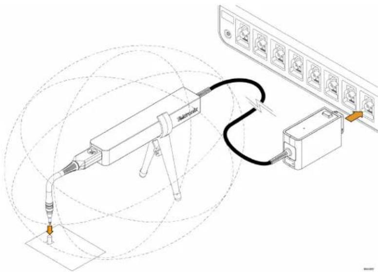
The unique common mode voltage range of the measurement system allows it to be used in the presence of high frequency/high voltage common mode signals. It is important to observe all precautions while using this product.

WARNING: Electrical shock can occur while using this measurement system. The system is intended to isolate the operator from hazardous input voltages (common mode voltages); the plastic case of the probe head and the shield on the probe tip do not supply safe isolation. Maintain the safe clearance from the probe head and probe tip while the measurement system is connected to the energized circuit as recommended in this document. Do not access the RF Burn Hazard Zone while taking measurements on a live circuit.
The following figure shows the components of the measurement system and the potential RF burn area when working with hazardous voltages. The RF burn area of 1m (40 in.) is indicated by the dashed lines surrounding the probe head.
natural_image
Technical diagram of a mechanical device connected to a control unit with multiple sensors (no text or symbols present)Figure 1: RF burn hazard zone around the probe head

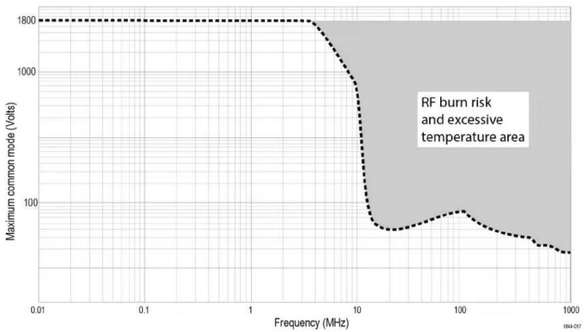
WARNING: Risk of RF burns. Refer to the following derating curve to identify the danger areas. To avoid RF burns, do not operate the probe within limits of the gray shaded area in the graph.

WARNING: There is a risk of burn from elevated temperatures on the tip when continuous wave or high duty cycle burst common mode signals are between about 10 MHz and 50 MHz. This causes the tip ferrites to dissipate significant power at voltages lower than found on the following graph. To avoid the burn risk, keep the tip temperature at 85°C (185°F) or lower by limiting the applied common mode voltage and/or duty cycle, lowering the ambient temperature, and/or applying forced convection airflow.
line
| Frequency (MHz) | Maximum common mode (Volts) | | --------------- | --------------------------- | | 0.01 | 1800 | | 0.1 | 1800 | | 1 | 1800 | | 10 | 100 | | 100 | 90 | | 1000 | 60 |Figure 2: Maximum safe handling limits for common mode voltages.
Compliance information
This section lists the safety and environmental standards with which the instrument complies. This product is intended for use by professionals and trained personnel only; it is not designed for use in households or by children.
Compliance questions may be directed to the following address:
Tektronix, Inc.
PO Box 500, MS 19-045
Beaverton, OR 97077, US
tek.com
Safety compliance
This section lists the safety standards with which the product complies and other safety compliance information.
EU declaration of conformity – low voltage
Compliance was demonstrated to the following specification as listed in the Official Journal of the European Union:
Low Voltage Directive 2014/35/EU.
- EN 61010-1. Safety Requirements for Electrical Equipment for Measurement, Control, and Laboratory Use – Part 1: General Requirements
- EN 61010-2-030. Safety Requirements for Electrical Equipment for Measurement, Control, and Laboratory Use – Part 2-030: Particular requirements for testing and measuring circuits
U.S. nationally recognized testing laboratory listing
- UL 61010-1. Safety Requirements for Electrical Equipment for Measurement, Control, and Laboratory Use – Part 1: General Requirements
- UL 61010-2-030. Safety Requirements for Electrical Equipment for Measurement, Control, and Laboratory Use – Part 2-030: Particular requirements for testing and measuring circuits
Canadian certification
- CAN/CSA-C22.2 No. 61010-1. Safety Requirements for Electrical Equipment for Measurement, Control, and Laboratory Use – Part 1: General Requirements
- CAN/CSA-C22.2 No. 61010-2-030. Safety Requirements for Electrical Equipment for Measurement, Control, and Laboratory Use – Part 2-030: Particular requirements for testing and measuring circuits
Additional compliances
- IEC 61010-1. Safety Requirements for Electrical Equipment for Measurement, Control, and Laboratory Use – Part 1: General Requirements
- IEC 61010-2-030. Safety Requirements for Electrical Equipment for Measurement, Control, and Laboratory Use – Part 2-030: Particular requirements for testing and measuring circuits
Equipment type
Test and measuring equipment.
Pollution degree description
A measure of the contaminants that could occur in the environment around and within a product. Typically the internal environment inside a product is considered to be the same as the external. Products should be used only in the environment for which they are rated.
- Pollution Degree 1. No pollution or only dry, nonconductive pollution occurs. Products in this category are generally encapsulated, hermetically sealed, or located in clean rooms.
- Pollution Degree 2. Normally only dry, nonconductive pollution occurs. Occasionally a temporary conductivity that is caused by condensation must be expected. This location is a typical office/home environment. Temporary condensation occurs only when the product is out of service.
- Pollution Degree 3. Conductive pollution, or dry, nonconductive pollution that becomes conductive due to condensation. These are sheltered locations where neither temperature nor humidity is controlled. The area is protected from direct sunshine, rain, or direct wind.
- Pollution Degree 4. Pollution that generates persistent conductivity through conductive dust, rain, or snow. Typical outdoor locations.
IP rating
IPx0 (as defined in IEC 60529).
Electrical ratings
Electrical ratings TICP025: Current 20mA, 250MHz
TICP050: Current 20mA, 500MHz
TICP100: Current 20mA, 1GHz
Max voltage to Earth 1300 V; Pollution degree 2; Max with transient level not to exceed 5kV
pk
1800 V; For use in a Pollution Degree 1 environment; Max with transient level not to exceed 5kV_pk
600 V for CAT III; Pollution degree 2
1000 V for CAT II; Pollution degree 2
Environmental compliance
This section provides information about the environmental impact of the product.
Product end-of-life handling
Observe the following guidelines when recycling an instrument or component:
Equipment recycling
Production of this equipment required the extraction and use of natural resources. The equipment may contain substances that could be harmful to the environment or human health if improperly handled at the product's end of life. To avoid release of such substances into the environment and to reduce the use of natural resources, we encourage you to recycle this product in an appropriate system that will ensure that most of the materials are reused or recycled appropriately.
This symbol indicates that this product complies with the applicable European Union requirements according to Directives 2012/19/EU and 2006/66/EC on waste electrical and electronic equipment (WEEE) and batteries. For information about recycling options, check the Tektronix Web site (www.tek.com/productrecycling).
Preface
This document provides information for installing and using the Tektronix TICP Series Active Isolated Current Shunt Probes.
The probe provide unparalleled bandwidth, accuracy, ease of use, and isolation in current shunt measurements.
natural_image
Technical line drawing of a medical or laboratory probe device with a control box and coiled cable (no text or symbols)Compensation box
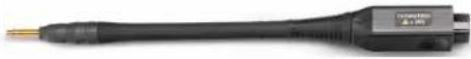
The TekVPI compensation (comp) box connects the measurement system to one of the input channels on the oscilloscope. Power is supplied to the measurement system through the TekVPI interface of the oscilloscope. The LEDs on the comp box provide a means for indicating the overall status of the probe.
Probe head
The probe head provides an interface between the device-under-test (DUT) and the compensation box. The probe head contains the isolation barrier that separates the DUT from the earth ground.
Probe tips
Probe tip options are available to connect the probe head to the DUT.
Key performance specifications and features
• Galvanic isolation between probe tip and the oscilloscope
• Available in three bandwidths: 1 GHz, 500 MHz, and 250 MHz
- Wide current measurement range determined by the shunt used with 1X, 10X or 100X probe tips
- Noise < 4.70 nV / (< 21 V RMS at 20 MHz)
- Up to 90 dB CMRR at 1 MHz
• Maximum common mode voltage: 1.8 kV; For use in a Pollution Degree 1 environment; transient level not to exceed 5 kV pk
• 1.5% DC gain accuracy
- Compatible with the 4, 5, and 6 Series MSO instruments, including the latest B models
- TekVPI™ interface enables control and probe configuration from the oscilloscope front panel or programming interface
Model overview
| Model Description |
| TICP025 250 MHz Tektronix Isolated Current Probe |
| TICP050 500 MHz Tektronix Isolated Current Probe |
| TICP100 1 GHz Tektronix Isolated Current Probe |
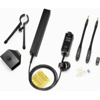
Standard accessories
The following table lists the accessories that are shipped with the probe.
| Accessory Description Part number | ||
 | 1X probe tip cable with MMCX connector TICPMM1 | |
 | 10X probe tip cable with MMCX connector TICPMM10 | |
 | SMA tip adapter TICPSMA | |
 | Clamp-on ferrite common mode choke 276-0905-XX | |
 | Bipod is used to hold the probe. 020-3210-XX | |
 | Tripod adapter for 1⁄4 in - 20 UNC thread accessories. 103-0508-XX | |
 | Probe tip adapter. Adapts an MMCX IsoVu tip to standard 0.100" spaced, 0.025" square pins. | 131-9717-XX |
Table continued...
| Accessory Description Part number | ||
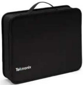 | Soft carrying case with foam insert. 016-2147-XX |
Recommended accessories
The following table lists optional accessories.
| Accessory Description Part number | ||
 | 100X probe tip with MMCX connector TICPMM100 | |
 | Square pin to MMCX adapter, 0.062" spacing 131-9677-XX | |
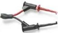 | MMCX to IC grabber lead 196-3546-XX | |
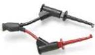 | Square pin to IC grabber lead 196-3547-XX | |
 | MicroCKT grabbers 206-0569-XX |
Operating information
Use this section to help you use the probe safely and effectively. Read all safety information before installing your measurement system to be aware of the operating and clearance requirements, including possible hazardous areas when the measurement system is connected to the DUT.
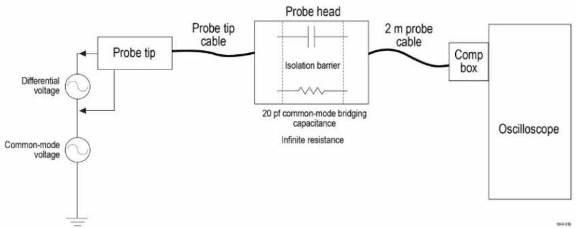
TICP block diagram
The following figure shows a block diagram of the Tektronix Active Isolated Current Shunt Probe.
flowchart
graph LR
    A["Common-mode voltage"] --> B["Differential voltage"]
    B --> C["Probe tip"]
    C --> D["Probe head"]
    D --> E["Isolation barrier"]
    E --> F["20 pf common-mode bridging capacitance"]
    F --> G["Infinite resistance"]
    G --> H["Comp box"]
    H --> I["Oscilloscope"]
    J["Probe tip cable"] --> D
    K["2 m probe cable"] --> H
The common-mode resistance and capacitance to earth ground is shown in the figure. The common-mode resistance is shown as infinite with the probe since it is galvanically isolated and can be ignored. The common-mode coupling capacitance to earth ground and the surrounding circuit is shown as the bridging capacitance. This capacitance will be approximately 20 pF when the probe head is placed 6 inches (15.25 cm) above a ground plane.
To minimize the effects of common-mode capacitive loading consider the following:
- When possible, choose a reference point in the device-under-test (DUT) that is static potential with respect to earth ground.
- Connect the coaxial (common) shield of the probe tip to the lowest impedance point of the circuit.
- Increasing the physical distance between the probe head and any conductive surface will reduce the capacitance.
- When using multiple TICP probes to measure different points in the circuit that do not have the same common-mode voltages, keep the probe heads separated to minimize the capacitive coupling.
Measurement system handling best practices
The measurement system consists of quality parts and should be treated with care to avoid damage or degrading the performance due to mishandling. Consider the following precautions when handling the probe and tips.
- Do not crush, crimp, or sharply bend the probe cable..
- Do not twist the cable.
- Do not allow kinks or knots to develop in the probe cable.
- Avoid putting tension on the probe cable.
- Do not pull or jerk the cable, especially when kinks or knots are present.
- Do not drop the probe head or comp box assembly. This can result in damage and misalignment of the internal components.
- Avoid over-bending the probe tips; do not exceed the minimum bend radius of 2.0 inches (5.1 cm).
- Avoid crushing the cables by accidentally running over the cable with a chair wheel or by dropping a heavy object onto the cable.
- Store the measurement system in the supplied carrying case when not in use.
Environmental requirements
| Characteristic Component | Operating Non-operating | ||
| Temperature Compensation | box and probe head 0°C to +50°C -20°C to +70°C | ||
| Tip cables and adapters -40°C to +85°C -40°C to +85°C | |||
| Humidity Compensation box | and probe head 5% to 85% relative humidity up to +40°C, 5% to 45% relative humidity up to +50°C, non-condensing | 5% to 85% relative humidity up to +40°C, 5% to 45% relative humidity up to +70°C, non-condensing | |
| Tip cables and adapters | |||
| Altitude All components Up to | 3,000 meters (9,842 feet) Up to 12,000 meters (39370 feet) |
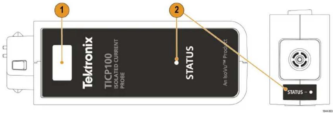
Controls and indicators
A description of the controls and indicators on the compensation box.
text_image
Tektronix TICP100 ISOLATED CURRENT PROBE STATUS An ISOV™ Product STATUS -- Latch release button. To disconnect the compensation (comp) box from the oscilloscope, press the latch release button and pull away from the instrument.
- STATUS indicators. LED lights that indicate the status of the probe. There is a status indicator on the top and back of the comp box. For more information on the state of the LED, see Table 8 on page 49
Cable flags
The flag on the cable provide a potential RF burn hazards warning.
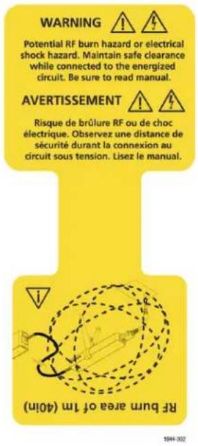
text_image
WARNING Potential RF burn hazard or electrical shock hazard. Maintain safe clearance while connected to the energized circuit. Be sure to read manual. AVERTISSEMENT Risque de brûlure RF ou de choc électrique. Observez une distance de sécurité durant la connexion au circuit sous tension. Lisez le manual. RF burn area of tim (40in) 184-92Probe tips
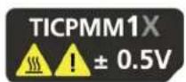
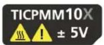
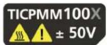
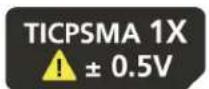
Each probe tip has a label that provides the maximum dynamic range and displays the attenuation factor.
1844-001
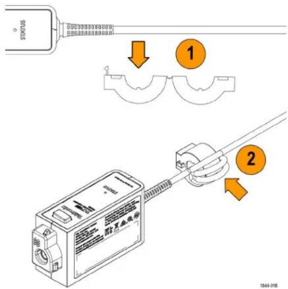
Ferrite clamp installation
The following steps describe installing the common mode ferrite clamp on the probe cable.
Procedure
text_image
STATUS ① ② 1944-018- Position the common mode ferrite clamp within 0.25 inches of the compensation box strain relief.
- Loop the cable around the open ferrite clamp five times and close the clamp.
Make sure the loops are as small as possible to maximize the effectiveness of the ferrite.
What to do next
To remove the ferrite clamp from the probe cable, insert a flat head screwdriver in the gap between the latches of the clamp and lift up.
Connecting to a circuit
The following steps describe the process for connecting the TICP Series probe to an oscilloscope and the device under test (DUT).
Before you begin
WARNING: Do not connect the measurement system to an energized circuit to avoid the risk of shock. Always de-energize the circuit-under-test before installing or removing the tip cable from the circuit-under-test. The plastic case of the probe head and the probe tip of the probe cable do not supply the isolation.
WARNING: To avoid the risk of electrical shock or RF burns while the DUT is energized, do not touch the probe head or probe tip while taking measurements. Always keep a 1 m (40 in.) clearance from the probe head during the measurement. See Figure 1 on page 11.
WARNING: To prevent the arc flash caused by a different potential, do not place the probe head or probe tip on the circuit that has the different voltage.
CAUTION: To avoid possible damage to the equipment, do not connect the coaxial (common) shield of the probe tip or SMA input to the high impedance portion of a circuit. The additional capacitance can cause circuit damage. Connect the coaxial (common) shield to the low impedance section of the circuit.
Note: Touching the probe head or probe tip cable when measuring a high frequency common mode signal increases the capacitive coupling and can degrade the common mode loading on the circuit-under-test.
Note: To avoid inaccurate measurements, do not stack the separate probe heads and keep cell phones at least three feet away while taking measurements.
About this task
Verify the DUT is not connected to an energized circuit. To obtain the most accurate measurement, allow the probe to warm up for 5 minutes.
Procedure
- Connect the compensation box an available channel on the oscilloscope.
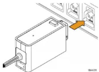
natural_image
Diagram of a mechanical device with a highlighted orange arrow pointing to a component (no text or symbols present)- Line up the probe tip and probe head IsoConnect™ connectors.
Take care to avoid bending or twisting the probe tip assembly during this process. - Connect the probe tip to the probe head.
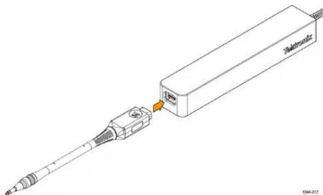
natural_image
Technical line drawing of a device with a connector and cable, no text or symbols present
Note: Connect the probe head to a bipod, tripod (with adapter), or a similar support. Using a support keeps the probe head steady, reducing the potential mechanical stresses at the electrical connection point of the DUT. The support also keeps the probe head away from surrounding circuits and conductive objects to minimize the parasitic capacitive coupling to these surroundings. The supplied tripod adapter is required to attaching the TICP Series probe to a tripod.
- Connect the probe tip end to the DUT.
If you are using MMCX tip, connect the tip to an MMCX connector or to a square pin adapter before connecting to the DUT. The adapters connect to square pins with either 0.100-inch (2.54 mm) spacing or 0.062-inch (1.57 mm) spacing.
- Set up the controls on the oscilloscope.
- Apply power to the DUT to take the measurement.
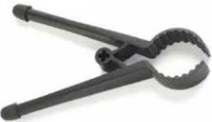
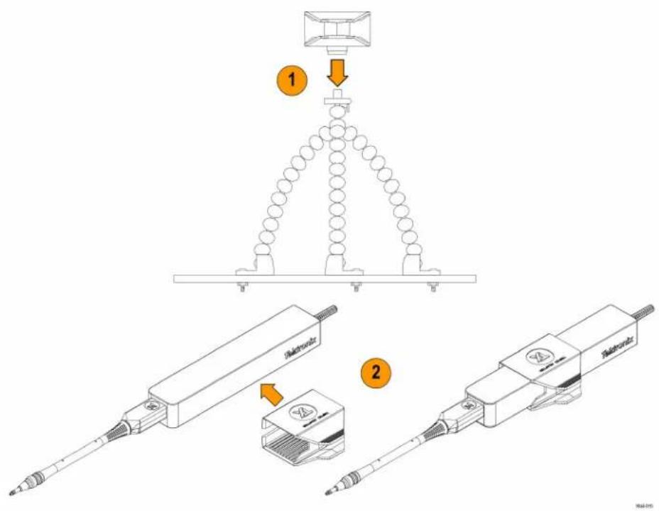
Tripod adapter installation
The following steps describe installing the tripod adapter to the probe head and attaching it to a tripod.
Procedure
text_image
Technical diagram illustrating a mechanical assembly with labeled components and directional arrows indicating assembly steps.- Attach the adapter to a compatible tripod.
The thread in the adapter is UNC ^1/4 -20. Make sure that the thread of the tripod is also UNC ^1/4 -20. - Open the clamp on the tripod adapter and attach it to the probe head.
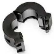
Bipod installation
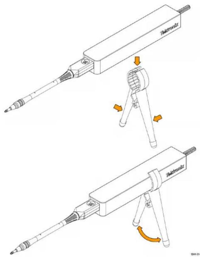
The following steps describe installing the bipod to the probe head.
Procedure
text_image
Technical diagram showing two types of soldering tools with labeled components and directional arrows indicating movement or force.- Squeeze the handles of the bipod together to open the clamp.
- Place the probe head into the clamp and release the handle so the probe is as the angle needed to connect to the DUT.
Connecting the SMA adapter
The following steps describe the process for connecting the TICPSMA SMA tip adapter to the probe head and SMA cable.
Before you begin

Note: It recommended to connect SMA cable to the SMA adapter first and then connect the SMA adapter to the probe head.
Procedure
text_image
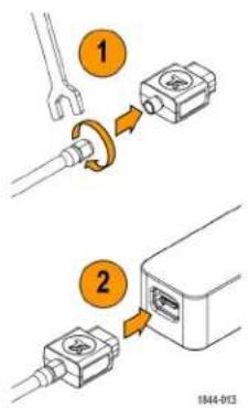
Diagram showing two steps of a mechanical or electrical component assembly, labeled 1 and 2, with numbered components and connection arrows.- Connect a SMA cable to the SMA adapter.
Use a SMA wrench to tighten the SMA cable to 8 in lbs. - Connect the SMA adapter to the probe head.
Installing the probe tip adapters
There are two Tektronix probe tip adapters to connect the MMCX probe tips to pins on the circuit board. The MMCX-to-0.1-inch (2.54 mm) pitch adapter and the MMCX-to-0.062-inch (1.57 mm) pitch adapter.
One end of each adapter has an MMCX socket for connection to an IsoVu MMCX tip cable. The other end of the adapter has a center pin socket and four common (shield) sockets around the outside of the adapter. Notches on the adapters can be used to locate the shield sockets. The procedure for installing these adapters are the same, the main difference is the spacing of the pins on the circuit board.
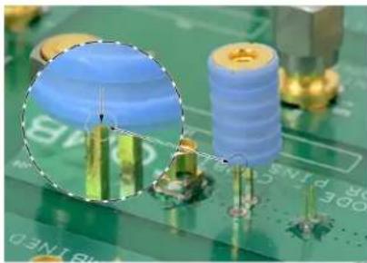
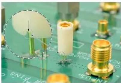
To install the adapters onto the square pins, line up the center of the adapter with the signal source pin on the circuit board. Use the notch on the adapter to align one of the shield sockets to the common pin on the circuit board. The following figures show examples of lining up the adapters on the circuit board.
To achieve the best electrical performance, especially the CMRR performance and EMI susceptibility, place the probe tip adapter as close as possible to the circuit board.
natural_image
Close-up of electronic components on a green circuit board, including a blue capacitor and gold pins (no visible text or symbols)Figure 3: Lining up the MMCX-to-0.1-inch (2.54 mm) adapter on the circuit board
natural_image
Close-up of electronic components on a green circuit board, including capacitors and connectors (no visible text or symbols)Figure 4: Lining up the MMCX-to-0.062-inch (1.57 mm) adapter on the circuit board
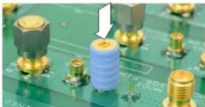
After lining up the adapters gently push down on the adapter to seat it in place on the circuit board.
natural_image
Close-up of a green circuit board with gold connectors and a blue solenoid component, no visible text or symbols.Figure 5: Pushing the MMCX-to-0.1-inch (2.54 mm) adapter in place
natural_image
Close-up of a green printed circuit board with gold connectors and a white cylindrical component (no visible text or symbols)Figure 6: Pushing the MMCX-to-0.062-inch (1.57 mm) adapter in place
Installing the square pins on the circuit board
The following figure and table shows the recommended clearance requirements for connecting the adapters to the square pins on the circuit board. The bottoms of the adapters are shown at the top.
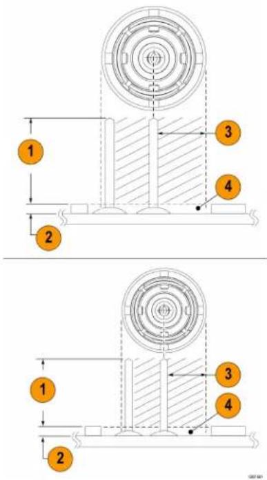
text_image
Technical diagram showing cross-sectional views of a mechanical assembly with numbered components and dimension annotations.Figure 7: Adapter clearance requirements
| Figure reference | Probe Tip Adapter, MMCX to 0.1” pitch sq. pin 0.635 mm (0.025 in) sq. pins | Probe Tip Adapter, MMCX to 0.062 in pitch sq. pin 0.406 mm (0.016 in) sq. pins |
| 1 Recommend maximum pin length 6.00 mm (0.235 in) Recommend maximum pin length 4.40 mm (0.170 in) | ||
| 2 Minimize area between adapter and circuit board | ||
| 3 Keep out area (diameter of each adapter) | ||
| 4 Avoid or minimize components within keep out area | ||
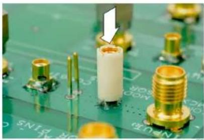
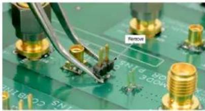
The 0.025-inch (0.635 mm) square pins should already be located on the circuit board. Some square pins might have headers installed on the circuit board. Tektronix recommends removing the plastic spacer from the square pins to gain closer access to the circuit board as
shown in the following figure to achieve the best electrical performance, especially CMRR. You might need to use a pair of tweezers to remove the spacer as shown in the figure.
text_image
Remove 1 N5 C01B TIN 1 N5 C01B TIN 1 N5 C01B TINFigure 8: Removing the header from square pins on the circuit board
Tektronix provides a set of solder pins (0.018-inch (0.46 mm) diameter) to install on the circuit board for use with the MMCX to 0.062-inch (1.57 mm) adapter. Use the soldering aide tool accessory (Tektronix part number, 003-1946-xx) to install these pins on the circuit board.
The solder pins are extremely small and can be challenging to handle. Tektronix recommends using tweezers and a magnifying tool when installing the pins on the circuit board.
The solder pins can be installed around a surface mounted component on the circuit board, but adequate clearance should be maintained for a good electrical connection for the adapter. Figure 7 on page 28

Note: The coaxial (common) shield of the probe tip and tip adapters should always be connected to the lowest impedance point (usually a circuit common or power supply rail) in the circuit-under-test (relative to the probe tip cable/center conductor) to obtain the most accurate waveform.
Use the following steps to install the solder pins using the soldering aide on the circuit board:
- Carefully insert the solder pins into the soldering aide as shown in the following illustration.
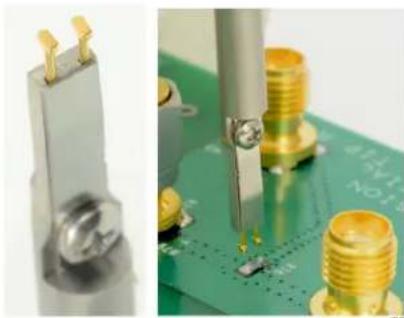
natural_image
Close-up of electronic components on a green circuit board, showing gold connectors and soldering tips (no visible text or symbols)Figure 9: Using the soldering aide to install the square pins on the circuit board
-
Use the soldering aide to hold the square pins in place while soldering the square pins to the circuit board.
-
If necessary apply a small amount of adhesive to further strengthen the connection to the circuit board. However, keep the height of the adhesive to a minimum to provide good electrical contact for the adapter. Figure 7 on page 28
Probe Setup menu
Use the probe setup menu to see probe information, perform self-calibration (SelfCal), perform AutoZero, change the range mode, and configure the range.
To access the Probe Setup menu on the oscilloscope, double-tap the corresponding analog channel badge on the settings bar and tap Probe Setup.
You will receive a warning message if you connect the probe to the oscilloscope without a probe tip attached. The following images display the menu with and without the tip warning.
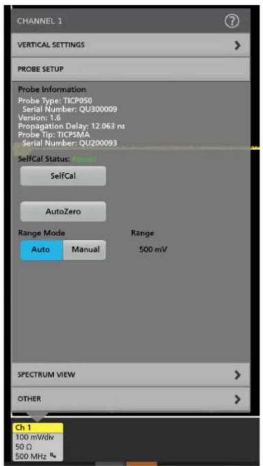
text_image
CHANNEL 1 VERTICAL SETTINGS PROBE SETUP Probe Information Probe Type: TICP050 Serial Number: QU300009 Version: 1.6 Propagation Delay: 12.063 ns Probe Tip: TICPSMA Serial Number: QU200093 SelfCal Status: SelfCal AutoZero Range Mode Range Auto Manual 500 mV SPECTRUM VIEW > OTHER > Ch 1 100 mV/div 50 Ω 500 MHz R
text_image
CHANNEL 1 VERTICAL SETTINGS PROBE SETUP Probe Information Probe Type: TICP050 Serial Number: QU300009 Version: 1.6 Propagation Delay: 11.903 ns Probe Tip: N/A Serial Number: N/A Error Information No probe tip detected. Please install a compatible probe tip. SelfCal Status: SelfCal AutoZero Range Mode Auto Manual Range 500 mV SPECTRUM VIEW > OTHER > Ch 1 No Tip 100 mV/div 50 Ω 500 MHzSelf-calibration
The self-calibration (SelfCal) function that corrects gain accuracy and DC offset. These parameters change as the probe warms up to the operating temperature and remain constant once the temperature reaches steady-state.
Check the SelfCal Status in the Probe Setup menu. The status indicates when SelfCal has Passed, Failed or if it is Recommended to run SelfCal.
To check the status of the SelfCal remotely, use the SELFCAL:STATE? PI command to determine self-calibration is RECOMMENDED, RUNNING, or PASSED.
It is recommended to run SelfCal again when there is a 10^ C change in ambient temperature or when the status is Recommended. To run a self-calibration use perform the following steps:
- Tap the channel badge corresponding to the channel you connected the probe to.
- In the channel menu, expand the Probe Setup tab.
- Tap the SelfCal button.
To run the self-calibration remotely, use the CH

Note: For the best results, run self-calibration while the probe is connected to the powered down DUT.
When using vertical scales of 10 mV/div or less, probe self-calibration should be run with the probe tip still attached and with no signal applied to the probe tip. Additionally, for the TICPSMA and TICPMX1X tips, it is recommended to leave a representative drive impedance (a powered-down DUT) connected to the probe tip during self-calibration.
At higher vertical scales, or in the particular use case of a TICPSMA or TICPMX1X tip driven by a very low impedance (a shunt resistor ≤5 ), an alternate approach of disconnecting the tip from the probe head may be used to insure no signal is applied during self-calibration.
The TICP Series probe takes five minutes to warm up and self-calibration takes less than two minutes to complete. The SelfCal Status will change to Passed or Failed.
AutoZero
AutoZero and self-calibration work on different parts of the measurement system. Self-calibration optimizes measurements through adjusting parameters in the probe. AutoZero is an oscilloscope function and is used when a displayed waveform is not centered correctly (for example; due to a small DC offset error). AutoZero automatically runs after self-calibration.
It is important to power-down the DUT or disconnect your probe from the DUT before running AutoZero.
Auto Range
The Range Mode is selectable for either Auto or Manual. When the Range Mode set to Auto, the probe range is automatically selected when the V/div knob on the oscilloscope is turned. The relationship between probe range and V/div setting matches that shown in Ranges and 4/5/6 Series MSO Volts/div settings table.
Ranges
The measurement system has a variety of ranges available for you to select, whether the probe is being used with or without a tip. This allows for tradeoffs to be made between noise and dynamic range depending on the needs of the measurement being made.

CAUTION: To avoid damaging the probe, do not exceed the Peak Voltage rating for a given tip or the probe head. The Maximum Non-Destruct Voltage limit (Peak Voltage) does not increase when the Probe Ranges are changed.
In 4, 5, and 6 Series MSO Instruments, the ranges are selectable when Range Mode is set to Manual. The recommended V/div settings are displayed in the table below. The ranges shown are for the probe SMA input and 1X tip. Multiply the range and V/div setting by the tip attenuation to get the values for a probe tip.
Table 1: Ranges and 4/5/6 Series MSO Volts/div settings
| 4/5/6 Series MSO probe ranges Recommended V/div setting |
| 20 mV 2 mV/div |
| 30 mV 5 mV/div |
Table continued...
4/5/6 Series MSO probe ranges Recommended V/div setting
| 45 mV 5 mV/div |
| 65 mV 10 mV/div |
| 90 mV 10 mV/div |
| 125 mV 20 mV/div |
| 175 mV 20 mV/div |
| 250 mV 20 mV/div |
| 350 mV 50 mV/div |
| 500 mV 100 mV/div |
When using a tip, the label of each probe tip shows the maximum dynamic range and the attenuation factor. When more sensitive ranges are selected, dynamic range is limited. Refer to the Linear differential input voltage range in the specifications table for more information.
Selecting a probe tip

CAUTION: Avoid over-voltage conditions that can damage or degrade the probe head input termination by selecting the correct probe tip. Selecting the correct probe tip attenuation factor is crucial to ensure that the probe head input termination is not degraded or damaged by an over-voltage condition. Select the probe tip that will provide the lowest attenuation possible for the signal being measured.
When selecting a probe tip for a particular application, consider the following questions:
- What is the maximum RMS/Peak Voltage at the test point being measured (for example, under a fault condition)?
- What is the minimum single-ended input resistance that my circuit can tolerate?
- How large of a signal do I want to display at one time on the oscilloscope?
- What sensitivity do I need (for example, the minimum V/div setting)?
The following table will help you select the correct probe tip. Start at the top of the table and work down. Choose the first tip that meets all of your criteria.
Table 2: Probe tip selection
| Probe tip | Most sensitive V/div setting Dynamic range | Maximum non-destruct voltage (DC + pk AC) | Single-ended input resistance | |
| TICPSMA 1 mV ±0.5 V ±3 V 50 Ω | ||||
| TICPMM1 1 mV ±0.5 V ±3 V 50 Ω | ||||
| TICPMM10 10 mV ±5V ±15 V 500 Ω | ||||
| TICPMM100 100 mV | ±50 V | ±60 V 5000 Ω | ||
For maximum non-destruct voltage refer to the Maximum differential input voltage vs frequency derating graphs.
Deskew
Each probe comes loaded with nominal propagation delay values that can be automatically applied through the Vertical menu on the oscilloscope. Deskew accuracy can be improved using a known signal and a deskew fixture. When the timing relationships between waveforms is critical, always deskew your test system with known equipment.
Input offset
The measurement system provides an adjustable input referred offset voltage.
This enables viewing a portion of the signal that is off-screen or examining sensitive behavior riding on a larger differential voltage. For example, a 0 V to 0.6 V step would normally exceed a ±0.5 V input range. By applying 250 mV of offset, the 600 mV step is brought into the dynamic range of the probe and can be viewed accurately. Offset is applied by the probe.
Voltage range
The probe is designed to enable characterization of high frequency circuits with a wide range of differential voltages in the presence of common mode voltages. Understanding the limits and differences between the voltage ratings as discussed in this section is essential to optimize signal fidelity and measurement accuracy.
Although the common mode voltage range of the probe is very large (1000 V CATII), the differential input range is limited and depends on the tip attenuation, the gain range selected, and the applied offset.
The input voltage conditions are divided into several different input ranges.
Common mode voltage range
The probe head is isolated from earth ground, making the common mode input range 1000 V CATII. The differential input range is more limited and refers to the signal that can be applied across the probe tip, regardless of the common mode voltage.
Differential voltage range refers to the actual measurement that will appear on the oscilloscope screen when using IsoVu™. For accurate results, the measurement must fall within the range of any applied offset ±V diff range of the tip.V meas =V offset ±V diff
Offset voltage range
Offset voltage can be applied through the oscilloscope Vertical menu settings. The input offset capability of the probe extends from ±0.5 V to ±50 V depending on the tip used. This offset is applied at the probe head and can be useful to bring applied signals within the dynamic range ( V_diff ) of the probe.
Maximum non-destruct differential voltage range
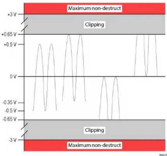
The maximum non-destruct differential input range is the maximum differential voltage that can be applied to the input without damaging the probe. This is a DC +peak AC rating (no portion of the differential input signal should exceed this value). The maximum non-destruct differential voltage varies from ±3 V to ±60 V depending on the probe tip being used. Exceeding these levels will cause permanent damage to components of the probe head.
Specifications
This chapter contains specifications for the instrument. All specifications are typical unless noted as guaranteed. Typical specifications are provided for your convenience but are not guaranteed. Specifications that are marked with the √ symbol are guaranteed and checked in Performance Verification.
All specifications are typical and apply to all models unless noted otherwise.
To meet specifications, these conditions must first be met:
- The instrument must be operating within the environmental limits described in this manual.
• The instrument must have been operating continuously for at least five minutes within the specified operating temperature range. - The measurement system is powered from a TekVPI compatible oscilloscope.
Warranted specifications describe guaranteed performance with tolerance limits or certain type-tested requirements.
Probe and tip overview
| Probes TICP100 TICP050 TICP025 | |||
| Bandwidth 1 GHz 500 MHz | 250 MHz | ||
| Rise time 400 ps 700 ps 1 | .4 ns | ||
| DC gain accuracy ±1.5% | |||
| Maximum common mode voltage | 1800 V; For use in a Pollution Degree 1 environment; Max with transient level not to exceed 5kV_pk | ||
| 1300 V; Pollution degree 2; Max with transient level not to exceed 5kV_pk | |||
| 600 V for CAT III; Pollution degree 2 | |||
| 1000 V for CAT II; Pollution degree 2 | |||
| RMS noise spectral density | 4.70 nV / (<21 V_RMS at 20 MHz) | ||
| Probe cable length 2 meters (78 inches) | |||
Input voltage range, input impedance
Differential input voltage range + offset range will not exceed maximum measurable input voltage. For example, offset limited to ±0.15 V in TICPSMA's ±0.5 V range. Full ±0.5 V offset available in the TICP Series probe's ±0.125 V range.
| Probe tips Differential | input voltage range | Offset range Maximum | measurable input voltage (Vpk) | Maximum non-destructive differential voltage | Input impedance |
| TICPSMA ±0.5 V ±0.5 | V 0.65 V | ±3 V; 3 V | RMS | 50 Ω || N.A. | |
| TICPMM1 | ±0.5 V ±0.5 V 0.65 V | ±3 V; 3 V | RMS | 50 Ω || N.A. | |
| TICPMM10 | ±5 V | ±5 V | 6.5 V | ±15 V; 15 VRMS | 500 Ω || <3 pF |
| TICPMM100 | ±50 V | ±50 V | 50 V | ±60 V; 60 VRMS | 5000 Ω || <3 pF |
line
| Condition | Voltage (V) | |---------------------|-------------| | Maximum non-destruct | +3 V | | Clipping | +0.65 V | | Clipping | 0 V | | Clipping | -0.35 V | | Clipping | -0.65 V | | Maximum non-destruct | -3 V |Figure 10: Differential input voltage range
Noise floor (A RMS)
$$ \text { Noise Floor } (A R M S) = \frac {4 . 7 0 \frac {n V}{\sqrt {H z}} \times \sqrt {\text { Bandwidth }}}{R _ {\text { shunt }}} $$
| Shunt selection 20 MHz 250 MHz 1 GHz | |||
| 50 Ω TICP as shunt 420 nA 1.5 μA 3.0 μA | |||
| 5 Ω shunt 4.2 μA 14.9 μA 29.7 μA | |||
| 1 Ω shunt 21 μA 74.3 μA 149 μA | |||
| 500 mΩ shunt 42 μA 149 μA 297 μA | |||
| 50 mΩ shunt 420 μA 1.5 mA 3.0 mA | |||
| 5 mΩ shunt 4.2 mA 14.9 mA 29.7 mA | |||
| 500 μΩ shunt 42 mA 149 mA 297 mA | |||
| 50 μΩ shunt 420 mA 1.5 A 3.0 A | |||
| 15 μΩ shunt 1.4 A 5.0 A 9.9 A |
Maximum measurable current
Maximum depends on shunt power rating.
$$ \text { Maximum Measurable Current } (A) = \frac {\text { Maximum Measurable Input } V _ {p k}}{R _ {\text { shunt }}} $$
| Shunt selection | TICPMM1 | TICPSMA | TICPMM10 | TICPMM100 |
| 50 Ω TICP as shunt | 13 mA | - | - | |
| 5 Ω shunt | 130 mA | 1.3 A | 10 A | |
| 1 Ω shunt | 650 mA | 6.5 A | 50 A | |
| Table continued... | ||||
| Shunt selection TICPMM1 TICPSMA TICPMM10 TICPMM100 | |||
| 500 mΩ shunt 1.3 A 13 A 100 A | |||
| 50 mΩ shunt 13 A 130 A 1.0 kA | |||
| 5 mΩ shunt 130 A 1.3 kA 10 kA | |||
| 500 μΩ shunt 1.3 kA 13 kA 100 kA | |||
| 50 μΩ shunt 13 kA | 130 kA | 1000 kA | |
| 15 μΩ shunt 43.3 kA | 433.3 kA | 3300 kA | |
Probe Ranges
Numbers are published for TICPSMA and TICPMM1 tips. For 10X or 100X tips, multiply by 10 or 100 respectively.
| Input range | Offset range | RMS noise spectral density ( V_RMS ) | Noise floor at 20 MHz ( V_RMS ) |
| ±0.5 V | ±0.15 V | 22.9 nV / | 102.5 V_RMS |
| ±0.35 V | ±0.30 V | 17.4 nV / | 77.8 V_RMS |
| ±0.25 V | ±0.40 V | 15.0 nV / | 67.2 V_RMS |
| ±0.175 V | ±0.475 V | 9.5 nV / | 42.4 V_RMS |
| ±0.125 V | ±0.5 V | 8.7 nV / | 38.9 V_RMS |
| ±0.09 V | ±0.5 V | 6.3 nV / | 28.3 V_RMS |
| ±0.065 V | ±0.5 V | 5.5 nV / | 24.7 V_RMS |
| ±0.045 V | ±0.5 V | 4.7 nV / | 21.2 V_RMS |
| ±0.03 V | ±0.5 V | 4.7 nV / | 21.2 V_RMS |
| ±0.02 V | ±0.5 V | 4.7 nV / | 21.2 V_RMS |
Common mode rejection ratio (CMRR)
| Probe tip | DC | 1 MHz | 100 MHz | 250 MHz | 500 MHz | 1 GHz |
| TICPSMA | 195 dB | 90 dB | 75 dB | 50 dB | 45 dB | 35 dB |
| TICPMM1 | 140 dB | 90 dB | 80 dB | 70 dB | 70 dB | 50 dB |
| TICPMM10 | 160 dB | 70 dB | 60 dB | 60 dB | 40 dB | 20 dB |
| TICPMM100 | 145 dB | 50 dB | 45 dB | 30 dB | 20 dB | 6 dB |
Application Examples
Application examples for Wide Bandgap (WBG) and PMIC power integrity.
WBG example (800V, 40 A typical; 0.125 Ω shunt)
In a 800 V SiC circuit switching at 40 A, a 125 mΩ shunt will produce a 5 V signal. To measure this using the TICP the 10X tip must be used. In the ±3.5 V range apply 24 A of offset.
The measurable current range goes from 52 A to -4 A. At these settings, the RMS noise floor at 250 MHz bandwidth is 2.2 mA RMS
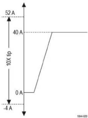
line
| Voltage (A) | Current (A) | |---|---| | 40 | 52 | | -4 | 0 | | 10X slip | 0 |PMIC power integrity (48 V, 3 mA typical; 1 Ω shunt)
On a 48 V PMIC bus, the standby current of 3mA will produce a 3mV signal on a 1 shunt. Use the 1X tip in the most sensitive ± 20mV range, apply offset to view the 3mA current and capture transients from 0A to 40mA with a RMS noise floor of 21.2 A
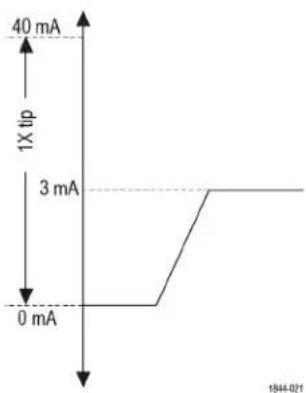
line
| Time (s) | Current (mA) | | :--- | :--- | | 0 | 0 | | 1 | 3 | | 2 | 40 |Electrical specifications
Analog bandwidth
| Probe tip Bandwidth | |
| TICPSMA >1 GHz | |
| TICPMM1 >1 GHz | |
| TICMM10 >1 GHz | |
| TICPMM100 >1 GHz |
Linearity Deviation of from best line is < ±2% of peak FS
Maximum deviation from linear regression expressed as a percentage of the specified dynamic range.
Input impedance
| Probe tip Input resistance Input capacitance | ||
| TICPMM1 50 ±0.5%, 49.75 to 50.25 | ||
| TICMM10 500 ±2%, 490 to 510 <3 pF | ||
| TICPMM100 5000 ±2%, 4900 to 5100 <3 pF |
Isolated guard line impedance >120 MΩ, \~17 pF (to earth ground)
Offset gain accuracy ±0.5%
Offset linearity ±0.1%
Operating voltage input range ±0.65 V maximum differential
Input coupling DC
DC balance < 0.1 divs
Operating random vibration 0.31 GRMS, 5-500 Hz, 10 minutes per axis, 3 axes (30 minutes total)
Frequency response graph
The following graph shows the frequency response for each probe.
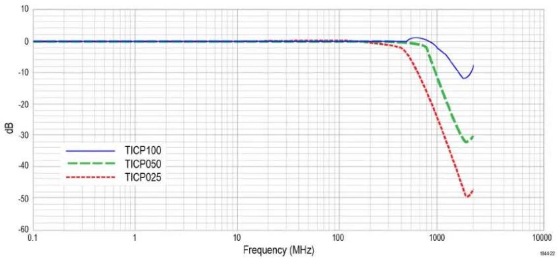
line
| Frequency (MHz) | TICP100 | TICP050 | TICP025 | | --------------- | ------- | ------- | ------- | | 0.1 | 0.0 | 0.0 | 0.0 | | 1 | 0.0 | 0.0 | 0.0 | | 10 | 0.0 | 0.0 | 0.0 | | 100 | 0.0 | 0.0 | 0.0 | | 1000 | -5.0 | -15.0 | -35.0 | | 10000 | -10.0 | -30.0 | -50.0 |Regulatory compliance
EMC Conforms to European Union EMC Directive (CE-marked)
Safety Conforms to European Union Low Voltage Directive (CE-marked)
Conforms to ANSI/UL61010-1 (CSA-marked)
Conforms to ANSI/UL61010-2-030 (CSA-marked)
Certified to CAN/CSA C22.2 No.61010-1 (CSA-marked)
Certified to CAN/CSA C22.2 No.61010-2-030 (CSA-marked)
RoHS Conforms to European Union Restrictions on Hazardous Substances (CE-marked)
Probe dimensions
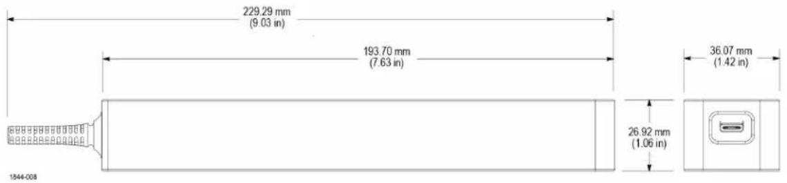
text_image
229.29 mm (9.03 in) 193.70 mm (7.63 in) 36.07 mm (1.42 in) 26.92 mm (1.06 in) 1844-008Figure 11: Probe head
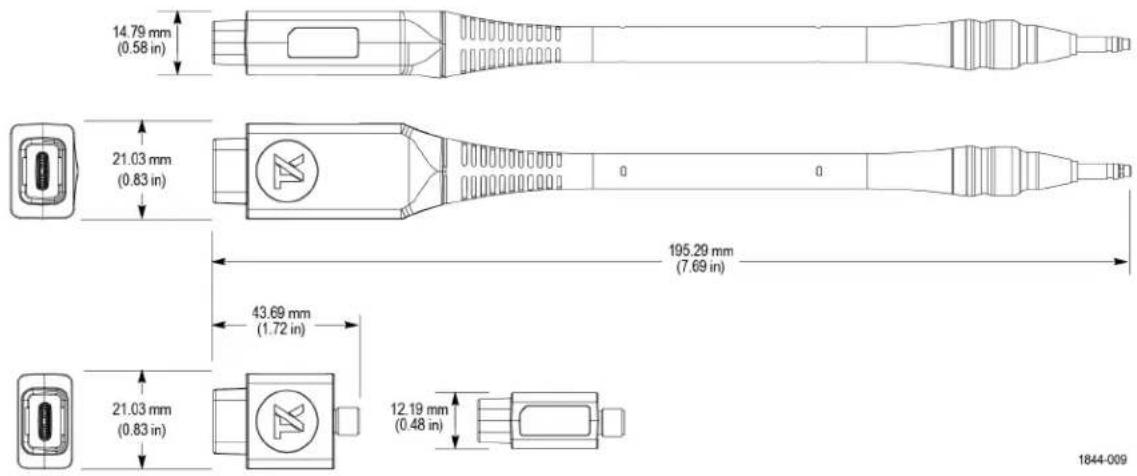
text_image
14.79 mm (0.58 in) 21.03 mm (0.83 in) 195.29 mm (7.69 in) 43.69 mm (1.72 in) 21.03 mm (0.83 in) 12.19 mm (0.48 in) 1844-009Figure 12: Probe tips
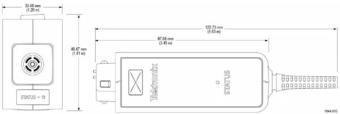
text_image
30.48 mm (1.20 in) 48.47 mm (1.91 in) 122.73 mm (4.83 in) 87.68 mm (3.45 in) STATUS TEKTRONIX STATUS STATUS 1844-010Figure 13: Compensation box
Performance verification procedures
Use the following procedures to verify the performance of the IsoVu measurement system. Before beginning the procedures, photocopy the test record and use it to record the performance results. Test record
Required equipment
The equipment required to perform the performance verification procedures are shown in the following table.
Table 3: Required equipment for performance verification
| Description Minimum requirements Example product | |
| Supported oscilloscope with TekVPI interface 50 Ω input support, fully compatible with TekVPI interface | Tektronix 5 Series B MSO |
| DC voltage source 3 mV to 4 V, ±0.1% accuracy Fluke 9500B Oscilloscope Calibrator with a Fluke 9500 Active Head | |
| SMA male short circuit connector cap (optional) Internally shorted, copper plated contact Fairview Microwave SC2135 | |
| Digital multimeter (DMM) 0.1% accuracy or better Tektronix DMM6500 | |
| One 50 Ω terminator Impedance 50 Ω; connectors: female BNC input, male BNC output | Tektronix part number 011-0049-XX |
| Precision termination test fixture Tektronix part number 067-3281-XX | |
| TekVPI calibration performance verification fixture | Tektronix part number 067-1701-XX |
System RMS Noise
This procedure verifies that the TICP Series probes are functioning and meet the warranted noise specification. The noise will be measured with no input signal at the most sensitive range.
Before you begin
- Turn on the TekVPI oscilloscope.
- Connect the TICP probe to the oscilloscope on channel 1 and remove the TICP probe tip (if attached).
- Allow the test equipment to warm up for 30 minutes at an ambient temperature of about 20 °C (68 °F).
About this task
This procedure is valid for all versions of the TICP Series probe.
Procedure
- Tap File > Default Setup.
- Run Signal Path Compensation, if recommended in Utility > Calibration...
- Run self-calibration (Self-calibration on page 30).
- Connect the TICPSMA probe tip to TICP probe.
- Connect the SMA short connector cap to TICPSMA.
- Enable the TICP channel and use the following Vertical menu settings:
a) Vertical Scale: 1 mV/div
- Edit Trigger menu settings as follows:
a) Type: Edge
b) Source: AC Line
c) Slope: Rising
d) Level: 0 V
e) Coupling: DC
- Edit Horizontal menu settings as follows:
a) Horizontal Scale: 100 μs/div
b) Record Length: 6.25 M
- Edit the following Acquisition menu setting:
a) Single Sequence Stop After: 1 Acquisitions
- Add a measurement with the following settings:
a) Amplitude Measurement: AC RMS
b) Source: CH 1
- Press the Single / Seq button to perform the measurement.
- Record the AC RMS measurement result in the test record table.
System RMS noise test record
Use the test record table for recording the results of the system RMS noise performance verification procedure.
Table 4: Test record table
| Model number: | Procedure performed by: |
| Serial number: | Date: |
| Probe Maximum noise Measured noise | ||
| TICP025 75 μV | rms | |
| TICP050 125 μV | rms | |
| TICP100 155 μV | rms | |
DC Gain Accuracy
This procedure verifies that the TICP Series probes are functioning and meet the warranted DC gain accuracy.
Before you begin
- Turn on the TekVPI oscilloscope.
- Connect a 067-3281-XX 50 Ω precision termination to the output of the 067-1701-XX fixture.
- Connect a DMM to the 50 Ω precision output with a BNC tee.
- Connect a BNC cable from the tee at the output of the 50 Ω precision termination to any other oscilloscope channel. Verify the channel is in 1 MΩ mode and 200 mV/div. This is used for proper grounding only.
- Connect the 067-1701-XX fixture into channel 1 on the oscilloscope.
- Connect the TICP Series probe into the 067-1701-XX fixture.
- Turn on the Fluke 9500B Oscilloscope Calibrator.
- Connect the Fluke 9530 Active Head to the Fluke 9500B on channel 1.
- Allow the test equipment to warm up for 30 minutes at an ambient temperature of about 20 °C (68 °F).
About this task
This procedure is valid for all versions of the TICP Series probe.
Procedure
- Tap File > Default Setup.
- Run Signal Path Compensation, if recommended in Utility > Calibration...
- Run self-calibration (Self-calibration on page 30).
- Connect the TICPSMA probe tip to TICP probe.
- Connect the TICPSMA to the Fluke 9500 Active Head.
-
Enable the TICP channel and use the following Vertical menu settings:
a) Range Mode: Manual
b) Range: 500 mV
c) Offset: 0 V -
On the Fluke 9500B, select Mode: Manual Waveform with the following settings:
a) Select Waveform: DC
b) Select 400 mV/div
c) Turn output ON
-
Press the Single / Seq button to perform the measurement.
-
Record the DC voltage on the precision 50 Ω resistor in the table.
-
Press invert voltage (+/-) button on the Fluke 9500B to apply -400 mV to the probe and record the output voltage in the table.
-
Repeat the entire procedure for the remaining ranges and record the values in the test record table.
DC Gain Accuracy test record
Use the test record table for recording the results of the DC gain accuracy performance verification procedure.
Table 5: Test record table
| Model number: | Procedure performed by: |
| Serial number: | Date: |
Probe gain is defined as the change in Output divided by the change in input.
Gain=(Measurement1-Measurement2)/(Input1-Input2)
| Range Input 1 | Input 2 Measured | output 1 | Measured output 2 | Calculated gain | Upper gain limit | Ideal gain Lower gain limit |
| 500 m +0.400 V | -0.400 V 1.010 | 1.000 0.990 | ||||
| 350 m +0.280 V | -0.280 V 1.443 | 1.429 1.415 | ||||
| 250 m +0.200 V | -0.200 V 2.020 | 2.000 1.980 | ||||
| 175 m +0.140 V | -0.140 V 2.886 | 2.857 2.828 | ||||
| 125 m +0.100 V | -0.100 V 4.040 | 4.000 3.960 | ||||
| 90 m +0.072 V | -0.072 V 5.612 | 5.556 5.500 | ||||
| 65 m +0.052 V | -0.052 V 7.769 | 7.692 7.615 | ||||
| 45 m +0.036 V | -0.036 V 11.222 | 11.111 11.000 | ||||
| 30 m +0.024 V | -0.024 V 16.834 | 16.667 16.500 | ||||
| 20 m +0.016 V | -0.016 V 25.250 | 25.000 24.750 |
DC Balance
This procedure verifies that the TICP Series probes are functioning and meet the warranted residual offset when input is zero and offset is zero.
Before you begin
- Turn on the TekVPI oscilloscope.
- Connect a 067-3281-XX 50 Ω precision termination to the output of the 067-1701-XX fixture.
- Connect a DMM to the 50 Ω precision output with a BNC tee.
- Connect a BNC cable from the tee at the output of the 50 Ω precision termination to any other oscilloscope channel. Verify the channel is in 1 MΩ mode and 200 mV/div. This is used for proper grounding only.
- Connect the 067-1701-XX fixture into channel 1 on the oscilloscope.
- Connect the TICP Series probe into the 067-1701-XX fixture.
- Allow the test equipment to warm up for 30 minutes at an ambient temperature of about 20 °C (68 °F).
About this task
This procedure is valid for all versions of the TICP Series probe.
Procedure
- Tap File > Default Setup.
- Run Signal Path Compensation, if recommended in Utility > Calibration...
- Run self-calibration (Self-calibration on page 30).
- Attach the TICPSMA probe tip to TICP probe.
- Enable the TICP channel and use the following Vertical menu setting:
a) Range mode: Manual
b) Probe range: 500 mV - Press the Single / Seq button to perform the measurement.
a) Measure the voltage on the output side of the precision 50 Ω termination with the DMM. - Repeat the entire procedure for the remaining ranges and record the values in the test record table.
DC Balance test record
Use the test record table for recording the results of the DC balance performance verification procedure.
Table 6: Test record table
| Model number: | Procedure performed by: |
| Serial number: | Date: |
The residual output for any range should be less than ±10 mV.
| Range Limit Measured | ||
| 500 mV ±10 mV | ||
| 350 mV ±10 mV | ||
| 250 mV ±10 mV | ||
| 175 mV ±10 mV | ||
| 125 mV ±10 mV | ||
| 90 mV ±10 mV | ||
| 65 mV ±10 mV | ||
| 45 mV ±10 mV | ||
| 30 mV ±10 mV | ||
| 20 mV ±10 mV |
Offset Gain Accuracy
This procedure verifies that the TICP Series probes are functioning and meet the warranted offset gain accuracy.
Before you begin
- Turn on the TekVPI oscilloscope.
- Connect a 067-3281-XX 50 Ω precision termination to the output of the 067-1701-XX fixture.
- Connect a DMM to the 50 Ω precision output with a BNC tee.
- Connect a BNC cable from the tee at the output of the 50 Ω precision termination to any other oscilloscope channel. Verify the channel is in 1 MΩ mode and 200 mV/div. This is used for proper grounding only.
- Connect the 067-1701-XX fixture into channel 1 on the oscilloscope.
- Connect the TICP Series probe into the 067-1701-XX fixture.
- Allow the test equipment to warm up for 30 minutes at an ambient temperature of about 20 °C (68 °F).
About this task
This procedure is valid for all versions of the TICP Series probe.
Procedure
- Tap File > Default Setup.
- Run Signal Path Compensation, if recommended in Utility > Calibration...
- Run self-calibration (Self-calibration on page 30).
- Attach the TICPSMA probe tip to TICP probe.
-
Attach the TICPSMA to the Fluke 9500 Active Head.
-
Enable the TICP channel and use the following Vertical menu settings:
a) Range: 20 mV
b) Offset: 20 mV/div
- On the Fluke 9500B, select Mode: Manual Waveform with the following settings:
a) Select Waveform: DC
b) Select 20 mV/div
c) Turn output ON
-
Press the Single / Seq button to perform the measurement.
a) Add the offset with value measured on the DMM. -
Repeat the entire procedure with all of the following oscilloscope offset and Fluke input voltage settings: 0.25 V, 0 V, -0.25 V, and -0.5 V.
Offset Gain Accuracy test record
Use the test record table for recording the results of the offset gain accuracy performance verification procedure.
Table 7: Test record table
| Model number: | Procedure performed by: |
| Serial number: | Date: |
- Input the offset voltages and corresponding measured mean result into Excel.
- Create a scatter plot of the data with offset voltages in the Y-axis and mean voltages in the X-axis.
- Add a trend line to the plot and select to show the equation.
The best fit of the data should have a slope between 0.995 and 1.005 to meet a 1% accuracy.
| Range 500 mV | measurement | 250 mV measurement | 0 V measurement | -250 mV measurement | -500 mV measurement | Limits Calculated | |
| 20 mV 0.995 < x | < | 1.005 |
Maintenance
Information to isolate possible failures and procedures for maintaining your probe.
Service offerings
Tektronix provides service to cover repair under warranty and other services that are designed to meet your specific service needs.
Tektronix service technicians are well equipped to service your probe. Services are provided at Tektronix Service Centers and on-site at your facility, depending on your location. Visit tek.com/service to view all available services. Check the status of your warranty at tek.com/warranty-status-search.
Cleaning

CAUTION: To prevent damage to the measurement system, do not expose it to sprays, liquids, or solvents. Avoid getting moisture inside the comp box or sensor head when cleaning the exterior.
Maintain the integrity of the connectors by keeping them free of contamination. Remove any debris from the connectors using low-pressure, clean, dry, compressed air.
Troubleshooting and error conditions
The following describes the state of each LED and possible problems that you might encounter when taking measurements with the probe. Use this as a quick troubleshooting reference before contacting Tektronix for service.
Table 8: STATUS LED descriptions
| LED Status Action | |||
| Green (Solid) Normal | operation - | ||
 | Green (Blinking) Bulk | power failure Try unplugging and plugging back in. Inspect probe/oscilloscope interface. Service of probe may be required. | |
 | Red (Solid) Probe application failure Try unplugging and plugging back in. Service of probe may be required. | ||
 | Red (Blinking) Probe application failure and bulk power failure | application failure and bulk power failure | Try unplugging and plugging back in. Inspect probe/oscilloscope interface. Service of probe and/or oscilloscope may be required. |
| [58Z7] | Red (Blinking • • – ) No power to the isolated side of the probe | No power to the isolated side of the probe | Try unplugging and plugging back in. Service of probe may be required. |
Table 9: Measurement problems and possible solutions
| Problem Solution | |
| DC offset is present in signal | Run self calibrationEnsure the input signal is within the selected dynamic range of the selected tip |
| Table continued... | |
| The Square Wave edge appears “smoothed”, rolled off, or uncompensated | ·Run self calibration·Make sure the oscilloscope bandwidth filter is set to full bandwidth·Make sure the input signal is not overdriving the probe input |
| The measured amplitude is smaller than expected | ·The input signal may be “railed”·Make sure the input signal is within the dynamic range of the selected probe tip·Apply offset to bring the input signal within the dynamic range of the selected probe tip |
| DC measurement inaccuracy | ·Run self calibration·Set the record length to at least 200 μs (longer is better) |
| There is too much noise and you cannot accurately measure small signals | ·Select a tip with lower attenuation·Set the oscilloscope vertical scale to a smaller value·Manually select a lower range to lower noise |
| There is no signal detected; the waveform is a flat line | ·Remove the tip and check its continuity, referencing the input impedance table |
| The probe head loses power intermittently | ·Make sure the probe head is within its operating temperature range·Add external cooling; such as a small desktop fan |
| There is too much common mode noise | ·Try to remove any accessories, flying leads, or exposed wires between the test point and the probe tip·Use an MMCX tip with an MMCX test point either designed into the board or as an unplanned test point |
| No tip detected warning | ·Detach and reattach the tip |
Repack the measurement system for shipment
If you need to return the measurement system to Tektronix for repair, use the original packaging. If this is unavailable or not fit for use, contact your Tektronix representative to obtain new packaging.
When you return the measurement system to Tektronix, attach a tag showing the following information:
• Name of the product owner
- Address of the owner
- Instrument serial number
- A description of problems encountered and/or service required
Remote programming
This sections describes commands and queries that can be sent to the sensor head when attached to a Tektronix oscilloscope. Long-form and short-form keywords are indicated with upper/lower case letters. The commands and queries are supported by most oscilloscopes; differences in supporting oscilloscopes, if any, are described with the commands.
For additional information, refer to the programmer documentation for your oscilloscope.
Command list
The commands and queries are supported by most oscilloscopes; differences in supporting oscilloscopes, if any, are described with the commands. For additional information, refer to the programmer documentation for your oscilloscope.
CH:PRObe? (Query Only)
This query-only command returns all information concerning the probe that is attached to the specified channel. The channel is specified by x.
Syntax CH
Examples CH2: PROBE? might return 1.0000E-01; RESISTANCE 1.0000E+07; UNITS "V"; ID: TYPE "10X"' SERNUMBER "N/A" for a 10X probe, indicating that (among other parameters) the attenuation factor for the probe attached to Channel 2 is 100.0 mV (assuming that probe units are set to volts).
CH:PRObe:AUTOZero (No Query Form)
This command executes the AutoZero function. The operation is entirely performed by the oscilloscope. The channel is specified by x.
Refer to the self-calibration procedure for information on performing the self calibration. Self-calibration
Syntax CH
Arguments EXECute sets the probe attached to the specified channel to AutoZero.
Examples CH1: PROBE:AUTOZERO EXECUTE sets the probe attached to the Channel 1 to autozero.
CH:PRObe:FORCEDRange
The command selects the dynamic range of probe (1 of 9) in +/-V. It is dependent on the attached probe tip. The channel is specified by x. The command should only be used when CH
Table 10: Probe tip cables and dynamic ranges
| Probe tip cable Dynamic Range +/-V |
| No tip or 1X tip 0.02 | 0.03 | 0.045 | 0.065 | 0.09 | 0.125 | 0.175 | 0.25 | 0.35 | 0.5 |
| 10X 0.2 | 0.3 | 0.45 | 0.65 | 0.9 | 1.25 | 1.75 | 2.5 | 3.5 | 5.0 |
| 100X 2 | 3 | 4.5 | 6.5 | 9 | 12.5 | 17.5 | 25 | 35 | 50 |
The query returns the dynamic range of the probe tip in +/-V.
| Syntax | CH2:PRObe:FORCEDRange <NR3> |
| CH2:PRObe:FORCEDRange? |
Arguments
| Examples | If a current probe is attached to the Channel 1 input, CH1: PROBE: FORCEDRANGE 5.0 sets the attached probe to its 5 V range.CH3: PROBE: FORCEDRANGE? might return 5.0000, indicating that the range of the probe attached to the Channel 3 is set to 5 V. |
CH:PRObe:GAIN? (Query Only)
The command returns the gain factor of the currently selected range (inverse of attenuation). The channel is specified by x.
Syntax CH
Examples CH2: PROBE: GAIN? might return 100.0000E-3, indicating that the attached 10X probe delivers 0.1 V to the Channel 2 BNC for every 1.0 V applied to the probe input.
CH:PRObe:ID? (Query Only)
This query-only command returns the type and serial number of the probe that is attached to the specified channel. The channel is specified by x.
Syntax CH
Examples CH2: PROBE: ID? might return "B010289"; "TICP100", indicating that a TICP100 probe with serial number B010289 is attached to Channel 2.
CH:PRObe:ID:SERnumber? (Query Only)
This query-only command returns the serial number of the probe that is attached to the specified channel. The channel is specified by x.

Note: For Level 0 and 1 probes, the serial number will be "N/A".
Syntax
CH<x>:PRObe:ID:SERnumber?
Examples
CH1: PROBE: ID: SERNUMBER? might return "B010289", indicating that the serial number of the probe attached to Channel 1 is B010289.
CH:PRObe:ID:TYPE? (Query Only)
This query-only command returns the type of probe that is attached to the specified channel. The channel is specified by x.
Syntax
CH<x>:PRObe:ID:TYPE?
Examples
CH1: PROBE: ID: TYPE? might return "TICP100", indicating that a TICP100 probe is attached to Channel 1.
CH:PRObe:SELFCal:State? (Query Only)
This query-only command returns the self-calibration state of RECOMMENDED, RUNNING, or PASSED. The channel is specified by x.
Syntax
CH<x>:PRObe:SELFCal:State?
Examples
CH1: PRObe: SELFCal: State? might return RUNNING, indicating that the Channel 1 probe is currently running a self-calibration.
CH:PRObe:SELFCal
This query-only command initiates self-calibration on the probe. The channel is specified by x.
Syntax
CH<x>:PRObe:SELFCal EXECUTE
Examples
CH1:PRObe:SELFCal EXECUTE runs self-calibration on the Channel 1 probe.
CH:PRObe:STATus? (Query Only)
This command queries the probe unsigned integer error value. The channel is specified by x.
Conditions Requires a probe that supports the relevant error messages.
Syntax
CH<x>:PRObe:STATUS?
Returns
Returns an integer number that represents the sum total of binary error bits B0 – B15. The error bits are not displayed; they are concatenated into the integer value. The following is a list of the error for each bit.
- B0 – Probe disabled
- B1 – Jaws open
• B2 – Over range
• B3 – Probe temperature out of limits
• B4 – Degauss needed
• B5 – Probe tip missing
- B6 – Probe tip failed
• B7 – Probe tip not supported
- B8 – self-calibration is needed or recommended (the query will return 256 in decimal format)
• B9 through B15 – Reserved
Examples
CH4: PROBE: STATUS? might return 2, indicating that the probe is reporting an open jaws error.
CH:PRObe:UNIts? (Query Only)
This query-only command returns a string describing the units of measure for the probe attached to the specified channel. The channel is specified by x.
Syntax
CH
Examples
CH4: PROBE: UNITS? might return "V", indicating that the unit of measure for the probe attached to Channel 4 is Volts.
CH:PROBECControl
This command sets or queries multirange probe range-control policy preference of the probe that is attached to CH
Syntax
CH
CH
Arguments
AUTO sets the values. The probe range is automatically calculated.
MANual allows you to select various valid values for the probe connected to a particular channel.
Examples
CH2: PROBECONTROL AUTO sets the values and the probe range is automatically calculated.
CH2: PROBECONTROL? might return MANUAL indicating that you can select various valid values for the probe connected to channel 2.
CH:PROBEFunc:EXTAtten
This command is used to specify the attenuation value as a multiplier to the given scale factor on the specified channel. The channel is specified by x.
The query form of this command returns the user-specified attenuation.
Syntax
CH
CH
Arguments
Examples
CH1: PROBEFUNC: EXTATTEN 167.00E-3 specifies an external attenuation, which is connected between the your input signal and the input of the probe attached to Channel 1.
CH2: PROBEFUNC: EXTATTEN? might return 1.0000E+00, indicating that the probe attached to Channel 2 is connected directly to the user's signal.
CH:PROBEFunc:EXTDBatten
This command sets or queries the input-output ratio (expressed in decibel units) of external attenuation or gain between the signal and the instrument input channels. The channel is specified by x.
The query form of this command returns the user-specified attenuation in decibels.
| Syntax | CH:PROBEFunc:EXTDBatten |
| CH:PROBEFunc:EXTDBatten? | |
| Arguments | is the attenuation value, which is specified in the range from -200.00 dB to 200.00 dB. |
| Examples | CH3:PROBEFUNC:EXTDBATTEN 2.5 specifies an external 2.5 dB attenuator on Channel 3. |
| CH1:PROBEFUNC:EXTDBATTEN? might return 2.5000E+00, indicating that the attenuation for Channel 1 is 2.5 dB. |
CH:PROBEFunc:EXTUnits
This command sets the unit of measurement for the external attenuator of the specified channel. The channel is specified by x. The alternate units are used if they are enabled. Use the CH
| Syntax | CH:PROBEFunc:EXTUnits |
| CH:PROBEFunc:EXTUnits? | |
| Arguments | indicates the attenuation unit of measurement for the specified channel. |
| Examples | CH4:PROBEFUNC:EXTUNITS "Pascals" sets the unit of measurement for the Channel 4 external attenuator. |
| CH2:PROBEFUNC:EXTUNITS? might return "Pascals", indicating that the Channel 2 external attenuator unit of measurement is Pascals. |
CH:PROBEFunc:EXTUnits:STATE
This command sets or queries the custom units enable state for the specified channel. The channel is specified by x.
| Syntax | CH< x>:PROBEFunc:EXTUnits:STATE {ON|OFF|<NR1>} |
| CH< x>:PROBEFunc:EXTUnits:STATE? |
Arguments OFF argument turns off external units.
ON argument turns on external units.
Examples CH2: PROBEFunc: EXTUnits: STATE ON turns on external units.
CH2: PROBEFunc:EXTUnits:STATE? might return 0, indicating that external units are off for the specified channel.
CH:PROBE:DYNAMICRANGE? (Query Only)
This command queries the dynamic range of the probe that is attached to the specified channel. The channel is specified by x.
Syntax
CH
Returns
The returned value is the delta between the current minimum and maximum range with some tolerance. It is also the delta between the probe range indicators (if currently displayed).
Examples
CH1: PROBE: DYNAMICRANGE? might return 1.3056, indicating that the dynamic range of the probe attached to the Channel 1 is set to 1.3056 V.
TICP Serie
Copyright © 2024, Tektronix. 2024 All rights reserved. Licensed software products are owned by Tektronix or its subsidiaries or suppliers, and are protected by national copyright laws and international treaty provisions. Tektronix products are covered by U.S. and foreign patents, issued and pending. Information in this publication supersedes that in all previously published material. Specifications and price change privileges reserved. All other trade names referenced are the service marks, trademarks, or registered trademarks of their respective companies.
TEKTRONIX and TEK are registered trademarks of Tektronix, Inc.
Tektronix, Inc.
14150 SW Karl Braun Drive
P.O. Box 500
Beaverton, OR 97077
US
For product information, sales, service, and technical support visit tek.com to find contacts in your area. For warranty information visit tek.com/warranty.
Inhalt
TEKTRONIX END USER LICENSE AGREEMENT....5
Third Party Software Licenses....6
Go to www.tek.com/en/eula to read the Tektronix End User License Agreement.

text_image
Blue QR code image, scannable for digital information retrievalThird Party Software Licenses
Freescale Kinetis Design Studio
This component module is generated by Processor Expert. Do not modify it.
Copyright : 1997 - 2015 Freescale Semiconductor, Inc.
All Rights Reserved.
Redistribution and use in source and binary forms, with or without modification, are permitted provided that the following conditions are met:
• Redistributions of source code must retain the above copyright notice, this list of conditions and the following disclaimer.
- Redistributions in binary form must reproduce the above copyright notice, this list of conditions and the following disclaimer in the documentation and/or other materials provided with the distribution.
- Neither the name of Freescale Semiconductor, Inc. nor the names of its contributors may be used to endorse or promote products derived from this software without specific prior written permission.
THIS SOFTWARE IS PROVIDED BY THE COPYRIGHT HOLDERS AND CONTRIBUTORS "AS IS" AND ANY EXPRESS OR IMPLIED WARRANTIES, INCLUDING, BUT NOT LIMITED TO, THE IMPLIED WARRANTIES OF MERCHANTABILITY AND FITNESS FOR A PARTICULAR PURPOSE ARE DISCLAIMED. IN NO EVENT SHALL THE COPYRIGHT HOLDER OR CONTRIBUTORS BE LIABLE FOR ANY DIRECT, INDIRECT, INCIDENTAL, SPECIAL, EXEMPLARY, OR CONSEQUENTIAL DAMAGES (INCLUDING, BUT NOT LIMITED TO, PROCUREMENT OF SUBSTITUTE GOODS OR SERVICES; LOSS OF USE, DATA, OR PROFITS; OR BUSINESS INTERRUPTION) HOWEVER CAUSED AND ON ANY THEORY OF LIABILITY, WHETHER IN CONTRACT, STRICT LIABILITY, OR TORT (INCLUDING NEGLIGENCE OR OTHERWISE) ARISING IN ANY WAY OUT OF THE USE OF THIS SOFTWARE, EVEN IF ADVISED OF THE POSSIBILITY OF SUCH DAMAGE.
http: www.freescale.com
mail: support@freescale.com
IAR Embedded Workbench for ARM
IARSourceLicense.txt Version 1.0
The following license agreement applies to linker command files, example projects unless another license is explicitly stated, the cstartup code, low_level_init.c, and some other low-level runtime library files.
Copyright 2012, IAR Systems AB.
This source code is the property of IAR Systems. The source code may only be used together with the IAR Embedded Workbench. Redistribution and use in source and binary forms, with or without modification, is permitted provided that the following conditions are met:
- Redistributions of source code, in whole or in part, must retain the above copyright notice, this list of conditions and the disclaimer below.
- IAR Systems name may not be used to endorse or promote products derived from this software without specific prior written permission.
THE SOFTWARE IS PROVIDED "AS IS" AND THE AUTHOR DISCLAIMS ALL WARRANTIES WITH REGARD TO THIS SOFTWARE INCLUDING ALL IMPLIED WARRANTIES OF MERCHANTABILITY AND FITNESS. IN NO EVENT SHALL THE AUTHOR BE LIABLE FOR ANY SPECIAL, DIRECT, INDIRECT, OR CONSEQUENTIAL DAMAGES OR ANY DAMAGES WHATSOEVER RESULTING FROM LOSS OF USE, DATA OR PROFITS, WHETHER IN AN ACTION OF CONTRACT, NEGLIGENCE OR OTHER TORTIOUS ACTION, ARISING OUT OF OR IN CONNECTION WITH THE USE OR PERFORMANCE OF THIS SOFTWARE.
natural_image
Technical diagram of a mechanical device connected to a control unit with multiple camera modules (no text or symbols present)line
| Frequency (MHz) | Maximum common mode (Volts) | | --------------- | --------------------------- | | 100 | 1000 | | 10 | 1000 | | 1 | 1000 | | 0.1 | 1000 | | 0.01 | 1000 |Beaverton, OR 97077, US
tek.com
natural_image
Technical line drawing of a medical or laboratory device with a labeled component (no text or symbols present)Kompensationsmodul
natural_image
Diagram of a mechanical device with a highlighted orange arrow pointing to a wall-mounted electrical outlet (no text or symbols present)natural_image
Technical line drawing of a soldering device with a labeled component (no text or symbols beyond label)
text_image
Technical diagram illustrating a mechanical assembly with labeled components and directional arrows indicating assembly steps.text_image
Technical diagram showing two types of soldering tools with labeled components and directional arrows indicating motion or assembly.text_image
Diagram showing two steps of inserting a connector into a device, labeled 1 and 2 with orange arrows indicating process flow.natural_image
Close-up of electronic components on a green circuit board, including a blue capacitor and resistors (no visible text or symbols)natural_image
Close-up of electronic components on a green circuit board, including capacitors and connectors (no visible text or symbols)natural_image
Close-up of a green circuit board with gold connectors and a blue ribbed component, no visible text or symbols.natural_image
Close-up of a green printed circuit board with gold connectors and a white cylindrical component (no visible text or symbols)text_image
Technical diagram showing cross-sectional views of a mechanical assembly with numbered components and dimension annotations.natural_image
Close-up of a green circuit board with gold connectors and soldering tools, no visible text or symbolsnatural_image
Close-up of electronic components on a green circuit board, showing gold connectors and soldering tools (no visible text or symbols)line
| Condition | Voltage (V) | | --------------------- | ----------- | | Maximum non-destruct | +3 V | | Clipping | +0.65 V | | Clipping | 0 V | | Clipping | -0.35 V | | Clipping | -0.65 V | | Maximum non-destruct | -3 V |$$ \text { Maximum Measurable Current } (A) = \frac {\text { Maximum Measurable Input } V _ {p k}}{R _ {\text { shunt }}} $$
line
| Time (μs) | Current (mA) | |---|---| | 0 | 0 | | 1 | 3 | | 2 | 40 |line
| Frequency (MHz) | TICP100 | TICP050 | TICP025 | | --------------- | ------- | ------- | ------- | | 0.1 | 0 | 0 | 0 | | 1 | 0 | 0 | 0 | | 10 | 0 | 0 | 0 | | 100 | 0 | 0 | 0 | | 1000 | -5 | -10 | -20 | | 10000 | -15 | -30 | -45 |CH:PRObe:FORCEDRange
CH:PRObe:ID:SERnumber? (Nur Abfrage)
CH
Beispiele
CH:PRObe:SELFCal:State? (Nur Abfrage)
CH
Beispiele
CH
Beispiele
Syntax CH
Copyright © 2024, Tektronix. 2024 All rights reserved. Licensed software products are owned by Tektronix or its subsidiaries or suppliers, and are protected by national copyright laws and international treaty provisions. Tektronix products are covered by U.S. and foreign patents, issued and pending. Information in this publication supersedes that in all previously published material. Specifications and price change privileges reserved. All other trade names referenced are the service marks, trademarks, or registered trademarks of their respective companies.
TEKTRONIX and TEK are registered trademarks of Tektronix, Inc.
Tektronix, Inc.
14150 SW Karl Braun Drive
P.O. Box 500
Beaverton, OR 97077
US
For product information, sales, service, and technical support visit tek.com to find contacts in your area. For warranty information visit tek.com/warranty.
Contents
TEKTRONIX END USER LICENSE AGREEMENT....5
Third Party Software Licenses....6
Go to www.tek.com/en/eula to read the Tektronix End User License Agreement.

text_image
Blue QR code image, scannable for digital information retrievalThird Party Software Licenses
Freescale Kinetis Design Studio
This component module is generated by Processor Expert. Do not modify it.
Copyright : 1997 - 2015 Freescale Semiconductor, Inc.
All Rights Reserved.
Redistribution and use in source and binary forms, with or without modification, are permitted provided that the following conditions are met:
• Redistributions of source code must retain the above copyright notice, this list of conditions and the following disclaimer.
- Redistributions in binary form must reproduce the above copyright notice, this list of conditions and the following disclaimer in the documentation and/or other materials provided with the distribution.
- Neither the name of Freescale Semiconductor, Inc. nor the names of its contributors may be used to endorse or promote products derived from this software without specific prior written permission.
THIS SOFTWARE IS PROVIDED BY THE COPYRIGHT HOLDERS AND CONTRIBUTORS "AS IS" AND ANY EXPRESS OR IMPLIED WARRANTIES, INCLUDING, BUT NOT LIMITED TO, THE IMPLIED WARRANTIES OF MERCHANTABILITY AND FITNESS FOR A PARTICULAR PURPOSE ARE DISCLAIMED. IN NO EVENT SHALL THE COPYRIGHT HOLDER OR CONTRIBUTORS BE LIABLE FOR ANY DIRECT, INDIRECT, INCIDENTAL, SPECIAL, EXEMPLARY, OR CONSEQUENTIAL DAMAGES (INCLUDING, BUT NOT LIMITED TO, PROCUREMENT OF SUBSTITUTE GOODS OR SERVICES; LOSS OF USE, DATA, OR PROFITS; OR BUSINESS INTERRUPTION) HOWEVER CAUSED AND ON ANY THEORY OF LIABILITY, WHETHER IN CONTRACT, STRICT LIABILITY, OR TORT (INCLUDING NEGLIGENCE OR OTHERWISE) ARISING IN ANY WAY OUT OF THE USE OF THIS SOFTWARE, EVEN IF ADVISED OF THE POSSIBILITY OF SUCH DAMAGE.
http: www.freescale.com
mail: support@freescale.com
IAR Embedded Workbench for ARM
IARSourceLicense.txt Version 1.0
The following license agreement applies to linker command files, example projects unless another license is explicitly stated, the cstartup code, low_level_init.c, and some other low-level runtime library files.
Copyright 2012, IAR Systems AB.
This source code is the property of IAR Systems. The source code may only be used together with the IAR Embedded Workbench. Redistribution and use in source and binary forms, with or without modification, is permitted provided that the following conditions are met:
- Redistributions of source code, in whole or in part, must retain the above copyright notice, this list of conditions and the disclaimer below.
- IAR Systems name may not be used to endorse or promote products derived from this software without specific prior written permission.
THE SOFTWARE IS PROVIDED "AS IS" AND THE AUTHOR DISCLAIMS ALL WARRANTIES WITH REGARD TO THIS SOFTWARE INCLUDING ALL IMPLIED WARRANTIES OF MERCHANTABILITY AND FITNESS. IN NO EVENT SHALL THE AUTHOR BE LIABLE FOR ANY SPECIAL, DIRECT, INDIRECT, OR CONSEQUENTIAL DAMAGES OR ANY DAMAGES WHATSOEVER RESULTING FROM LOSS OF USE, DATA OR PROFITS, WHETHER IN AN ACTION OF CONTRACT, NEGLIGENCE OR OTHER TORTIOUS ACTION, ARISING OUT OF OR IN CONNECTION WITH THE USE OR PERFORMANCE OF THIS SOFTWARE.
natural_image
Technical diagram of a medical or laboratory setup with a device connected to a device mounted on a wall, showing no visible text or symbols.line
| Frequency (MHz) | Maximum common mode (Volts) | | --------------- | --------------------------- | | 100 | 1000 | | 10 | 1000 | | 1 | 1000 | | 0.1 | 1000 | | 0.01 | 1000 |natural_image
Technical line drawing of a laboratory probe with a control box and probe tube (no text or symbols)natural_image
Diagram of a mechanical device with an orange arrow pointing to a component, no text or symbols presentnatural_image
Technical line drawing of a soldering device with a labeled component (no text or symbols beyond label)
text_image
Technical diagram illustrating a mechanical assembly with labeled components and directional arrows indicating assembly steps.text_image
Technical diagram showing two types of soldering tools with labeled components and directional arrows indicating motion or assembly.text_image
Diagram showing two steps of a mechanical or electrical component assembly, labeled 1 and 2, with numbered components and connection arrows.natural_image
Close-up of electronic components on a green circuit board, including a blue component and a metallic sensor (no visible text or symbols)natural_image
Close-up of electronic components on a green circuit board, including gold connectors and white cylindrical pins (no visible text or symbols)natural_image
Close-up of a green printed circuit board with gold connectors and a blue coil component, no visible text or symbols.natural_image
Close-up of a green printed circuit board with gold connectors and a white cylindrical component (no visible text or symbols)text_image
Technical diagram showing cross-sectional views of a mechanical assembly with numbered components and dimension annotations.natural_image
Close-up of a green circuit board with gold connectors and soldering wires, no visible text or symbolsnatural_image
Close-up of two electronic components: a metallic connector and gold-colored connectors on a green circuit board (no visible text or symbols)line
| Condition | Voltage (V) | | --------------------- | ----------- | | Maximum non-destruct | +3 V | | Clipping | +0.65 V | | Clipping | 0 V | | Clipping | -0.35 V | | Clipping | -0.65 V | | Maximum non-destruct | -3 V |$$ \text { Maximum Measurable Current } (A) = \frac {\text { Maximum Measurable Input } V _ {p k}}{R _ {\text { shunt }}} $$
line
| Time (μs) | Current (mA) | |---|---| | 0 | 0 | | 1 | 3 | | 2 | 40 |line
| Frequency (MHz) | TICP100 | TICP050 | TICP025 | | --------------- | ------- | ------- | ------- | | 0.1 | 0 | 0 | 0 | | 1 | 0 | 0 | 0 | | 10 | 0 | 0 | 0 | | 100 | 0 | 0 | 0 | | 1000 | -10 | -30 | -45 | | 10000 | -15 | -35 | -50 |CH:PRObe:FORCEDRange
CH:PRObe:ID:SERnumber? (solo consulta)
CH<x>:PRObe:ID:SERnumber?
Ejemplos
CH:PRObe:SELFCal:State? (solo consulta)
CH<x>:PRObe:SELFCal:State?
Ejemplos
CH:PRObe:STATus? (solo consulta)
CH:PRObe:UNIts? (solo consulta)
Sintaxis CH
Copyright © 2024, Tektronix. 2024 All rights reserved. Licensed software products are owned by Tektronix or its subsidiaries or suppliers, and are protected by national copyright laws and international treaty provisions. Tektronix products are covered by U.S. and foreign patents, issued and pending. Information in this publication supersedes that in all previously published material. Specifications and price change privileges reserved. All other trade names referenced are the service marks, trademarks, or registered trademarks of their respective companies.
TEKTRONIX and TEK are registered trademarks of Tektronix, Inc.
Tektronix, Inc.
14150 SW Karl Braun Drive
P.O. Box 500
Beaverton, OR 97077
US
For product information, sales, service, and technical support visit tek.com to find contacts in your area. For warranty information visit tek.com/warranty.
Table des matières
TEKTRONIX END USER LICENSE AGREEMENT....5
Third Party Software Licenses....6
Go to www.tek.com/en/eula to read the Tektronix End User License Agreement.

text_image
Blue QR code image, scannable for digital information retrievalThird Party Software Licenses
Freescale Kinetis Design Studio
This component module is generated by Processor Expert. Do not modify it.
Copyright : 1997 - 2015 Freescale Semiconductor, Inc.
All Rights Reserved.
Redistribution and use in source and binary forms, with or without modification, are permitted provided that the following conditions are met:
• Redistributions of source code must retain the above copyright notice, this list of conditions and the following disclaimer.
- Redistributions in binary form must reproduce the above copyright notice, this list of conditions and the following disclaimer in the documentation and/or other materials provided with the distribution.
- Neither the name of Freescale Semiconductor, Inc. nor the names of its contributors may be used to endorse or promote products derived from this software without specific prior written permission.
THIS SOFTWARE IS PROVIDED BY THE COPYRIGHT HOLDERS AND CONTRIBUTORS "AS IS" AND ANY EXPRESS OR IMPLIED WARRANTIES, INCLUDING, BUT NOT LIMITED TO, THE IMPLIED WARRANTIES OF MERCHANTABILITY AND FITNESS FOR A PARTICULAR PURPOSE ARE DISCLAIMED. IN NO EVENT SHALL THE COPYRIGHT HOLDER OR CONTRIBUTORS BE LIABLE FOR ANY DIRECT, INDIRECT, INCIDENTAL, SPECIAL, EXEMPLARY, OR CONSEQUENTIAL DAMAGES (INCLUDING, BUT NOT LIMITED TO, PROCUREMENT OF SUBSTITUTE GOODS OR SERVICES; LOSS OF USE, DATA, OR PROFITS; OR BUSINESS INTERRUPTION) HOWEVER CAUSED AND ON ANY THEORY OF LIABILITY, WHETHER IN CONTRACT, STRICT LIABILITY, OR TORT (INCLUDING NEGLIGENCE OR OTHERWISE) ARISING IN ANY WAY OUT OF THE USE OF THIS SOFTWARE, EVEN IF ADVISED OF THE POSSIBILITY OF SUCH DAMAGE.
http: www.freescale.com
mail: support@freescale.com
IAR Embedded Workbench for ARM
IARSourceLicense.txt Version 1.0
The following license agreement applies to linker command files, example projects unless another license is explicitly stated, the cstartup code, low_level_init.c, and some other low-level runtime library files.
Copyright 2012, IAR Systems AB.
This source code is the property of IAR Systems. The source code may only be used together with the IAR Embedded Workbench. Redistribution and use in source and binary forms, with or without modification, is permitted provided that the following conditions are met:
- Redistributions of source code, in whole or in part, must retain the above copyright notice, this list of conditions and the disclaimer below.
- IAR Systems name may not be used to endorse or promote products derived from this software without specific prior written permission.
THE SOFTWARE IS PROVIDED "AS IS" AND THE AUTHOR DISCLAIMS ALL WARRANTIES WITH REGARD TO THIS SOFTWARE INCLUDING ALL IMPLIED WARRANTIES OF MERCHANTABILITY AND FITNESS. IN NO EVENT SHALL THE AUTHOR BE LIABLE FOR ANY SPECIAL, DIRECT, INDIRECT, OR CONSEQUENTIAL DAMAGES OR ANY DAMAGES WHATSOEVER RESULTING FROM LOSS OF USE, DATA OR PROFITS, WHETHER IN AN ACTION OF CONTRACT, NEGLIGENCE OR OTHER TORTIOUS ACTION, ARISING OUT OF OR IN CONNECTION WITH THE USE OR PERFORMANCE OF THIS SOFTWARE.
Attention aux hautes tensions
natural_image
Technical diagram of a scientific instrument connected to a device with wiring, showing no text or symbols present.line
| Frequency (MHz) | Maximum common mode (Volts) | | --------------- | --------------------------- | | 100 | 1000 | | 10 | 1000 | | 1 | 1000 | | 0.1 | 1000 | | 0.01 | 1000 |natural_image
Technical line drawing of a laboratory probe with a control box and probe tube (no text or symbols)natural_image
Diagram of a mechanical device with a highlighted orange arrow pointing to a wall-mounted socket (no text or symbols present)natural_image
Technical line drawing of a soldering device with a labeled component (no text or symbols beyond label)
text_image
Technical diagram illustrating a mechanical assembly with labeled components and directional arrows indicating assembly steps.text_image
Technical diagram showing two types of soldering tools with labeled components and directional arrows indicating motion or assembly.text_image
Diagram showing two steps of a mechanical or electrical component assembly, labeled 1 and 2, with numbered components and connection arrows.natural_image
Close-up of electronic components on a green circuit board, including a blue capacitor and a blue resistor (no visible text or symbols)natural_image
Close-up of electronic components on a green circuit board, including capacitors and connectors (no visible text or symbols)natural_image
Close-up of a green circuit board with gold connectors and a blue ribbed component, no visible text or symbols.natural_image
Close-up of a green printed circuit board with gold connectors and a white cylindrical component (no visible text or symbols)text_image
Technical diagram showing cross-sectional views of a mechanical assembly with numbered components and dimension annotations.natural_image
Close-up of a green circuit board with gold pins and tweezers, no visible text or symbolsnatural_image
Close-up of electronic components on a green circuit board, showing gold connectors and soldering tools (no visible text or symbols)line
| Condition | Voltage (V) | | --------------------- | ----------- | | Maximum non-destruct | +3 V | | Clipping | +0.65 V | | Clipping | 0 V | | Clipping | -0.35 V | | Clipping | -0.65 V | | Maximum non-destruct | -3 V |$$ \text { Maximum Measurable Current } (A) = \frac {\text { Maximum Measurable Input } V _ {p k}}{R _ {\text { shunt }}} $$
| Shunt sélectionné | TICPMM1 | TICPSMA | TICPMM10 | TICPMM100 |
| TICP 50 Ω en tant que shunt | 13 mA | - | - | |
| Shunt 5 Ω | 130 mA | 1,3 A | 10 A | |
| Shunt 1 Ω | 650 mA | 6,5 A | 50 A | |
line
| Time (s) | Current (mA) | | :--- | :--- | | 0 | 0 | | 1 | 3 | | 2 | 40 |line
| Frequency (MHz) | TICP100 | TICP050 | TICP025 | | --------------- | ------- | ------- | ------- | | 0.1 | 0 | 0 | 0 | | 1 | 0 | 0 | 0 | | 10 | 0 | 0 | 0 | | 100 | 0 | 0 | 0 | | 1000 | -10 | -30 | -45 | | 10000 | -15 | -35 | -50 |CH:PRObe:FORCEDRange
CH2:PRObe:FORCEDRange
CH2:PRObe:FORCEDRange?
CH:PRObe:ID:SERnumber? (Requête uniquement)
CH
Exemples
CH:PRObe:SELFCal:State? (Requête uniquement)
CH
Exemples
CH
Exemples
CH:PRObe:UNIts? (Requête uniquement)
Copyright © 2024, Tektronix. 2024 All rights reserved. Licensed software products are owned by Tektronix or its subsidiaries or suppliers, and are protected by national copyright laws and international treaty provisions. Tektronix products are covered by U.S. and foreign patents, issued and pending. Information in this publication supersedes that in all previously published material. Specifications and price change privileges reserved. All other trade names referenced are the service marks, trademarks, or registered trademarks of their respective companies.
TEKTRONIX and TEK are registered trademarks of Tektronix, Inc.
Tektronix, Inc.
14150 SW Karl Braun Drive
P.O. Box 500
Beaverton, OR 97077
US
For product information, sales, service, and technical support visit tek.com to find contacts in your area. For warranty information visit tek.com/warranty.
Sommario
TEKTRONIX END USER LICENSE AGREEMENT....5
Third Party Software Licenses....6
Go to www.tek.com/en/eula to read the Tektronix End User License Agreement.

text_image
Blue QR code image, scannable for digital information retrievalThird Party Software Licenses
Freescale Kinetis Design Studio
This component module is generated by Processor Expert. Do not modify it.
Copyright : 1997 - 2015 Freescale Semiconductor, Inc.
All Rights Reserved.
Redistribution and use in source and binary forms, with or without modification, are permitted provided that the following conditions are met:
• Redistributions of source code must retain the above copyright notice, this list of conditions and the following disclaimer.
- Redistributions in binary form must reproduce the above copyright notice, this list of conditions and the following disclaimer in the documentation and/or other materials provided with the distribution.
- Neither the name of Freescale Semiconductor, Inc. nor the names of its contributors may be used to endorse or promote products derived from this software without specific prior written permission.
THIS SOFTWARE IS PROVIDED BY THE COPYRIGHT HOLDERS AND CONTRIBUTORS "AS IS" AND ANY EXPRESS OR IMPLIED WARRANTIES, INCLUDING, BUT NOT LIMITED TO, THE IMPLIED WARRANTIES OF MERCHANTABILITY AND FITNESS FOR A PARTICULAR PURPOSE ARE DISCLAIMED. IN NO EVENT SHALL THE COPYRIGHT HOLDER OR CONTRIBUTORS BE LIABLE FOR ANY DIRECT, INDIRECT, INCIDENTAL, SPECIAL, EXEMPLARY, OR CONSEQUENTIAL DAMAGES (INCLUDING, BUT NOT LIMITED TO, PROCUREMENT OF SUBSTITUTE GOODS OR SERVICES; LOSS OF USE, DATA, OR PROFITS; OR BUSINESS INTERRUPTION) HOWEVER CAUSED AND ON ANY THEORY OF LIABILITY, WHETHER IN CONTRACT, STRICT LIABILITY, OR TORT (INCLUDING NEGLIGENCE OR OTHERWISE) ARISING IN ANY WAY OUT OF THE USE OF THIS SOFTWARE, EVEN IF ADVISED OF THE POSSIBILITY OF SUCH DAMAGE.
http: www.freescale.com
mail: support@freescale.com
IAR Embedded Workbench for ARM
IARSourceLicense.txt Version 1.0
The following license agreement applies to linker command files, example projects unless another license is explicitly stated, the cstartup code, low_level_init.c, and some other low-level runtime library files.
Copyright 2012, IAR Systems AB.
This source code is the property of IAR Systems. The source code may only be used together with the IAR Embedded Workbench. Redistribution and use in source and binary forms, with or without modification, is permitted provided that the following conditions are met:
- Redistributions of source code, in whole or in part, must retain the above copyright notice, this list of conditions and the disclaimer below.
- IAR Systems name may not be used to endorse or promote products derived from this software without specific prior written permission.
THE SOFTWARE IS PROVIDED "AS IS" AND THE AUTHOR DISCLAIMS ALL WARRANTIES WITH REGARD TO THIS SOFTWARE INCLUDING ALL IMPLIED WARRANTIES OF MERCHANTABILITY AND FITNESS. IN NO EVENT SHALL THE AUTHOR BE LIABLE FOR ANY SPECIAL, DIRECT, INDIRECT, OR CONSEQUENTIAL DAMAGES OR ANY DAMAGES WHATSOEVER RESULTING FROM LOSS OF USE, DATA OR PROFITS, WHETHER IN AN ACTION OF CONTRACT, NEGLIGENCE OR OTHER TORTIOUS ACTION, ARISING OUT OF OR IN CONNECTION WITH THE USE OR PERFORMANCE OF THIS SOFTWARE.
natural_image
Technical diagram of a mechanical device connected to a control unit, with no visible text or symbols.line
| Frequency (MHz) | Maximum common mode (Volts) | | --------------- | --------------------------- | | 100 | 1000 | | 10 | 1000 | | 1 | 1000 | | 0.1 | 1000 | | 0.01 | 1000 |Beaverton, OR 97077, US
tek.com
natural_image
Technical line drawing of a medical or laboratory probe device with a control box and coiled cable (no text or symbols)natural_image
Diagram of a mechanical device with an orange arrow pointing to a component, no text or symbols presentnatural_image
Technical line drawing of a soldering device with a labeled component (no text or symbols beyond label)
text_image
Technical diagram illustrating a mechanical assembly with labeled components and directional arrows indicating assembly steps.text_image
Diagram showing two steps of inserting a connector into a device, labeled 1 and 2 with orange arrows indicating process flow.natural_image
Close-up of electronic components on a green circuit board, including a blue capacitor and a blue resistor (no visible text or symbols)natural_image
Close-up of electronic components on a green circuit board, including capacitors and connectors (no visible text or symbols)natural_image
Close-up of a green circuit board with gold connectors and a blue ribbed component, no visible text or symbols.natural_image
Close-up of a green printed circuit board with gold connectors and a white cylindrical component (no visible text or symbols)text_image
Technical diagram showing cross-sectional views of a mechanical assembly with numbered components and dimension annotations.natural_image
Close-up of electronic components including a metallic connector and gold connectors on a green circuit board (no visible text or symbols)line
| Condition | Voltage (V) | | --------------------- | ----------- | | Maximum non-destruct | +3 V | | Clipping | +0.65 V | | Clipping | 0 V | | Clipping | -0.35 V | | Clipping | -0.65 V | | Maximum non-destruct | -3 V |$$ \text { Maximum Measurable Current } (A) = \frac {\text { Maximum Measurable Input } V _ {p k}}{R _ {\text { shunt }}} $$
line
| Time (μs) | Current (mA) | |---|---| | 0 | 0 | | 1 | 3 | | 2 | 40 |line
| Frequency (MHz) | TICP100 | TICP050 | TICP025 | | --------------- | ------- | ------- | ------- | | 0.1 | 0 | 0 | 0 | | 1 | 0 | 0 | 0 | | 10 | 0 | 0 | 0 | | 100 | 0 | 0 | 0 | | 1000 | -5 | -10 | -20 | | 10000 | -15 | -30 | -45 |CH:PRObe? (solo query)
CH:PRObe:FORCEDRange
CH:PRObe:GAIN? (solo query)
CH:PRObe:ID? (solo query)
Sintassi CH
CH:PRObe:ID:SERnumber? (solo query)
CH
Esempi
CH:PRObe:ID:TYPE? (solo query)
CH:PRObe:SELFCal:State? (solo query)
CH
Esempi
CH
Esempi
CH:PRObe:STATus? (solo query)
CH:PRObe:UNIts? (solo query)
Sintassi CH
CH:PROBE:DYNAMICRANGE? (solo query)
Copyright © 2024, Tektronix. 2024 All rights reserved. Licensed software products are owned by Tektronix or its subsidiaries or suppliers, and are protected by national copyright laws and international treaty provisions. Tektronix products are covered by U.S. and foreign patents, issued and pending. Information in this publication supersedes that in all previously published material. Specifications and price change privileges reserved. All other trade names referenced are the service marks, trademarks, or registered trademarks of their respective companies.
TEKTRONIX and TEK are registered trademarks of Tektronix, Inc.
Tektronix, Inc.
14150 SW Karl Braun Drive
P.O. Box 500
Beaverton, OR 97077
US
For product information, sales, service, and technical support visit tek.com to find contacts in your area. For warranty information visit tek.com/warranty.
目次
TEKTRONIX END USER LICENSE AGREEMENT....5
Third Party Software Licenses....6
安全性に関する重要な情報....7
安全にご使用いただくために……7
火災や人体への損傷を避けるには……7
プローブとテスト・リード......8
Go to www.tek.com/en/eula to read the Tektronix End User License Agreement.

text_image
Blue QR code image, scannable for digital information retrievalThird Party Software Licenses
Freescale Kinetis Design Studio
This component module is generated by Processor Expert. Do not modify it.
Copyright : 1997 - 2015 Freescale Semiconductor, Inc.
All Rights Reserved.
Redistribution and use in source and binary forms, with or without modification, are permitted provided that the following conditions are met:
• Redistributions of source code must retain the above copyright notice, this list of conditions and the following disclaimer.
- Redistributions in binary form must reproduce the above copyright notice, this list of conditions and the following disclaimer in the documentation and/or other materials provided with the distribution.
- Neither the name of Freescale Semiconductor, Inc. nor the names of its contributors may be used to endorse or promote products derived from this software without specific prior written permission.
THIS SOFTWARE IS PROVIDED BY THE COPYRIGHT HOLDERS AND CONTRIBUTORS "AS IS" AND ANY EXPRESS OR IMPLIED WARRANTIES, INCLUDING, BUT NOT LIMITED TO, THE IMPLIED WARRANTIES OF MERCHANTABILITY AND FITNESS FOR A PARTICULAR PURPOSE ARE DISCLAIMED. IN NO EVENT SHALL THE COPYRIGHT HOLDER OR CONTRIBUTORS BE LIABLE FOR ANY DIRECT, INDIRECT, INCIDENTAL, SPECIAL, EXEMPLARY, OR CONSEQUENTIAL DAMAGES (INCLUDING, BUT NOT LIMITED TO, PROCUREMENT OF SUBSTITUTE GOODS OR SERVICES; LOSS OF USE, DATA, OR PROFITS; OR BUSINESS INTERRUPTION) HOWEVER CAUSED AND ON ANY THEORY OF LIABILITY, WHETHER IN CONTRACT, STRICT LIABILITY, OR TORT (INCLUDING NEGLIGENCE OR OTHERWISE) ARISING IN ANY WAY OUT OF THE USE OF THIS SOFTWARE, EVEN IF ADVISED OF THE POSSIBILITY OF SUCH DAMAGE.
http: www.freescale.com
mail: support@freescale.com
IAR Embedded Workbench for ARM
IARSourceLicense.txt Version 1.0
The following license agreement applies to linker command files, example projects unless another license is explicitly stated, the cstartup code, low_level_init.c, and some other low-level runtime library files.
Copyright 2012, IAR Systems AB.
This source code is the property of IAR Systems. The source code may only be used together with the IAR Embedded Workbench. Redistribution and use in source and binary forms, with or without modification, is permitted provided that the following conditions are met:
- Redistributions of source code, in whole or in part, must retain the above copyright notice, this list of conditions and the disclaimer below.
- IAR Systems name may not be used to endorse or promote products derived from this software without specific prior written permission.
THE SOFTWARE IS PROVIDED "AS IS" AND THE AUTHOR DISCLAIMS ALL WARRANTIES WITH REGARD TO THIS SOFTWARE INCLUDING ALL IMPLIED WARRANTIES OF MERCHANTABILITY AND FITNESS. IN NO EVENT SHALL THE AUTHOR BE LIABLE FOR ANY SPECIAL, DIRECT, INDIRECT, OR CONSEQUENTIAL DAMAGES OR ANY DAMAGES WHATSOEVER RESULTING FROM LOSS OF USE, DATA OR PROFITS, WHETHER IN AN ACTION OF CONTRACT, NEGLIGENCE OR OTHER TORTIOUS ACTION, ARISING OUT OF OR IN CONNECTION WITH THE USE OR PERFORMANCE OF THIS SOFTWARE.
安全性に関する重要な情報
natural_image
Technical diagram of a medical or laboratory setup with a syringe connected to a device, showing wiring and alignment patterns (no text or symbols present)line
| Frequency (MHz) | Maximum common mode (Volts) | | --------------- | --------------------------- | | 0.01 | 1000 | | 0.1 | 1000 | | 1 | 1000 | | 10 | 100 | | 100 | 10 | | 1000 | 1 | | 1800 | 0.01 |Beaverton, OR 97077, US
tek.com
安全適合性
natural_image
Technical line drawing of a medical or laboratory probe device with a control box and cable (no text or symbols)補正ボックス
text_image
STXUS 1 2 1544-018natural_image
Diagram of a device with connectors and wiring, showing an orange arrow pointing to a wall-mounted electrical outlet (no text or symbols present)natural_image
Technical line drawing of a soldering device with a rectangular box labeled 'Yaketsink' and a probe inserted into it (no text beyond label)
text_image
Technical diagram illustrating a mechanical assembly with labeled components and directional arrows indicating assembly steps.text_image
Technical diagram showing two types of soldering tools with labeled components and directional arrows indicating motion or assembly.text_image
Diagram showing two steps of inserting a connector into an Ethernet port, labeled with numbered instructions.natural_image
Close-up of electronic components on a green circuit board, with a magnified inset showing a blue component detail (no readable text or symbols)natural_image
Close-up of electronic components on a green circuit board, including gold connectors and white cylindrical pins (no visible text or symbols)natural_image
Close-up of a green printed circuit board with gold connectors and a blue threaded component, no visible text or symbols.natural_image
Close-up of a green printed circuit board with gold connectors and a white cylindrical component (no visible text or symbols)natural_image
Close-up of a green circuit board with gold components and tweezers, no visible text or symbolsnatural_image
Close-up of electronic components including a metallic connector and gold-colored connectors on a green circuit board (no visible text or symbols)line
| Condition | Voltage (V) | | --------------------- | ----------- | | Maximum non-destruct | +3 V | | Clipping | +0.65 V | | Clipping | 0 V | | Clipping | -0.35 V | | Clipping | -0.65 V | | Maximum non-destruct | -3 V |图10:差動入力電圧範囲
ノイズ・フロア(ARMS)
$$ \text { Noise Floor } (A R M S) = \frac {4 . 7 0 \frac {n V}{\sqrt {H z}} \times \sqrt {\text { Bandwidth }}}{R _ {\text { shunt }}} $$
$$ \text { Maximum Measurable Current } (A) = \frac {\text { Maximum Measurable Input } V _ {p k}}{R _ {s h u n t}} $$
line
| Time (s) | Current (mA) | | :--- | :--- | | 0 | 0 | | 1 | 3 | | 2 | 40 |電気仕様
line
| Frequency (MHz) | TICP100 | TICP050 | TICP025 | | --------------- | ------- | ------- | ------- | | 0.1 | 0.0 | 0.0 | 0.0 | | 1 | 0.0 | 0.0 | 0.0 | | 10 | 0.0 | 0.0 | 0.0 | | 100 | 0.0 | 0.0 | 0.0 | | 1000 | -5.0 | -15.0 | -35.0 | | 10000 | -10.0 | -30.0 | -50.0 |規制適合性
CH:PRObe:FORCEDRange
Register your product
tek.com/register
Copyright © 2024, Tektronix. 2024 All rights reserved. Licensed software products are owned by Tektronix or its subsidiaries or suppliers, and are protected by national copyright laws and international treaty provisions. Tektronix products are covered by U.S. and foreign patents, issued and pending. Information in this publication supersedes that in all previously published material. Specifications and price change privileges reserved. All other trade names referenced are the service marks, trademarks, or registered trademarks of their respective companies.
TEKTRONIX and TEK are registered trademarks of Tektronix, Inc.
Tektronix, Inc.
14150 SW Karl Braun Drive
P.O. Box 500
Beaverton, OR 97077
US
For product information, sales, service, and technical support visit tek.com to find contacts in your area. For warranty information visit tek.com/warranty.
Inhoudsopgave
TEKTRONIX END USER LICENSE AGREEMENT....5
Third Party Software Licenses....6
Go to www.tek.com/en/eula to read the Tektronix End User License Agreement.

text_image
Blue QR code image, scannable for digital information retrievalThird Party Software Licenses
Freescale Kinetis Design Studio
This component module is generated by Processor Expert. Do not modify it.
Copyright : 1997 - 2015 Freescale Semiconductor, Inc.
All Rights Reserved.
Redistribution and use in source and binary forms, with or without modification, are permitted provided that the following conditions are met:
• Redistributions of source code must retain the above copyright notice, this list of conditions and the following disclaimer.
- Redistributions in binary form must reproduce the above copyright notice, this list of conditions and the following disclaimer in the documentation and/or other materials provided with the distribution.
- Neither the name of Freescale Semiconductor, Inc. nor the names of its contributors may be used to endorse or promote products derived from this software without specific prior written permission.
THIS SOFTWARE IS PROVIDED BY THE COPYRIGHT HOLDERS AND CONTRIBUTORS "AS IS" AND ANY EXPRESS OR IMPLIED WARRANTIES, INCLUDING, BUT NOT LIMITED TO, THE IMPLIED WARRANTIES OF MERCHANTABILITY AND FITNESS FOR A PARTICULAR PURPOSE ARE DISCLAIMED. IN NO EVENT SHALL THE COPYRIGHT HOLDER OR CONTRIBUTORS BE LIABLE FOR ANY DIRECT, INDIRECT, INCIDENTAL, SPECIAL, EXEMPLARY, OR CONSEQUENTIAL DAMAGES (INCLUDING, BUT NOT LIMITED TO, PROCUREMENT OF SUBSTITUTE GOODS OR SERVICES; LOSS OF USE, DATA, OR PROFITS; OR BUSINESS INTERRUPTION) HOWEVER CAUSED AND ON ANY THEORY OF LIABILITY, WHETHER IN CONTRACT, STRICT LIABILITY, OR TORT (INCLUDING NEGLIGENCE OR OTHERWISE) ARISING IN ANY WAY OUT OF THE USE OF THIS SOFTWARE, EVEN IF ADVISED OF THE POSSIBILITY OF SUCH DAMAGE.
http: www.freescale.com
mail: support@freescale.com
IAR Embedded Workbench for ARM
IARSourceLicense.txt Version 1.0
The following license agreement applies to linker command files, example projects unless another license is explicitly stated, the cstartup code, low_level_init.c, and some other low-level runtime library files.
Copyright 2012, IAR Systems AB.
This source code is the property of IAR Systems. The source code may only be used together with the IAR Embedded Workbench. Redistribution and use in source and binary forms, with or without modification, is permitted provided that the following conditions are met:
- Redistributions of source code, in whole or in part, must retain the above copyright notice, this list of conditions and the disclaimer below.
- IAR Systems name may not be used to endorse or promote products derived from this software without specific prior written permission.
THE SOFTWARE IS PROVIDED "AS IS" AND THE AUTHOR DISCLAIMS ALL WARRANTIES WITH REGARD TO THIS SOFTWARE INCLUDING ALL IMPLIED WARRANTIES OF MERCHANTABILITY AND FITNESS. IN NO EVENT SHALL THE AUTHOR BE LIABLE FOR ANY SPECIAL, DIRECT, INDIRECT, OR CONSEQUENTIAL DAMAGES OR ANY DAMAGES WHATSOEVER RESULTING FROM LOSS OF USE, DATA OR PROFITS, WHETHER IN AN ACTION OF CONTRACT, NEGLIGENCE OR OTHER TORTIOUS ACTION, ARISING OUT OF OR IN CONNECTION WITH THE USE OR PERFORMANCE OF THIS SOFTWARE.
text_image
Technical diagram showing a sensor device connected to an electrical module with labeled components and wiring connections.line
| Frequency (MHz) | Maximum common mode (Volts) | | --------------- | --------------------------- | | 100 | 1000 | | 10 | 1000 | | 1 | 1000 | | 0.1 | 1000 | | 0.01 | 1000 |Beaverton, OR 97077, US
tek.com
Canadese certificering
natural_image
Technical line drawing of a medical or laboratory probe device with a control unit and coiled cable (no text or symbols)Compensatiebox
natural_image
Diagram of a device with an orange arrow pointing to a wall-mounted electrical outlet (no text or symbols present)natural_image
Technical line drawing of a device with an orange arrow pointing to a connector labeled 'Electronix' (no other text or symbols)
text_image
Technical diagram illustrating a mechanical assembly with labeled components and directional arrows indicating assembly steps.text_image
Technical diagram showing two types of soldering tools with labeled components and directional arrows indicating motion or assembly.text_image
Diagram showing two steps of inserting a connector into a device, labeled 1 and 2 with orange arrows indicating process flow.natural_image
Close-up of a green circuit board with electronic components and a magnified inset showing a blue component (no readable text or symbols)natural_image
Close-up of electronic components on a green circuit board, including capacitors and connectors (no visible text or symbols)natural_image
Close-up of a green circuit board with gold connectors and a blue coil component, no visible text or symbolsnatural_image
Close-up of a green printed circuit board with gold connectors and a white cylindrical component (no visible text or symbols)text_image
Technical diagram showing cross-sectional views of a mechanical assembly with numbered components and dimension annotations.Figuur 7: Afstandsvereisten adapter
natural_image
Close-up of electronic components on a green circuit board, showing soldering and gold-colored connectors (no visible text or symbols)line
| Condition | Voltage (V) | | ------------------- | ----------- | | Maximum non-destruct | +3 V | | Clipping | +0.65 V | | Clipping | 0 V | | Clipping | -0.35 V | | Clipping | -0.65 V | | Maximum non-destruct | -3 V |$$ \text { Maximum Measurable Current } (A) = \frac {\text { Maximum Measurable Input } V _ {p k}}{R _ {\text { shunt }}} $$
line
| Voltage (A) | Current (A) | |---|---| | 0 | 0 | | 40 | 52 | | -4 | -4 | 10X Vpline
| Time (t/p) | Current (mA) | | :--- | :--- | | 0 | 0 | | 1 | 3 | | 2 | 40 |Elektrische specificaties
Analoge bandbreedte
| Sondepunt Bandbreedte | |
| TICPSMA >1 GHz | |
| TICPMM1 >1 GHz | |
| TICMM10 >1 GHz | |
| TICPMM100 >1 GHz |
line
| Frequency (MHz) | TICP100 | TICP050 | TICP025 | | --------------- | ------- | ------- | ------- | | 0.1 | 0 | 0 | 0 | | 1 | 0 | 0 | 0 | | 10 | 0 | 0 | 0 | | 100 | 0 | 0 | 0 | | 1000 | -10 | -30 | -45 | | 10000 | -15 | -35 | -50 |Versterking = (Meting1-Meting2)/(Invoer1-Invoer2)
| Bereik Invoer | 1 Invoer 2 Gemeten | uitvoer 1 | Gemeten uitvoer 2 | Berekende versterking | Bovengrens versterking | Ideale versterking | Ondergrens versterking | |
| 500 m +0,400 | V -0,400 V 1,010 | 1,000 0,990 | ||||||
| 350 m +0,280 | V -0,280 V 1,443 | 1,429 1,415 | ||||||
| 250 m +0,200 | V -0,200 V 2,020 | 2,000 1,980 | ||||||
| 175 m +0,140 | V -0,140 V 2,886 | 2,857 2,828 | ||||||
| 125 m +0,100 | V -0,100 V 4,040 | 4,000 3,960 | ||||||
| 90 m +0,072 V | -0,072 V 5,612 | 5,556 5,500 | ||||||
| 65 m +0,052 V | -0,052 V 7,769 | 7,692 7,615 | ||||||
| 45 m +0,036 V | -0,036 V 11,222 | 11,111 11,000 | ||||||
| 30 m +0,024 V | -0,024 V 16,834 | 16,667 16,500 | ||||||
| 20 m +0,016 V | -0,016 V 25,250 | 25,000 24,750 | ||||||
DC-balans
CH:PRObe? (Query Only)
CH:PRObe:AUTOZero (No Query Form)
CH:PRObe:FORCEDRange
CH:PRObe:GAIN? (Query Only)
CH:PRObe:ID? (Query Only)
CH:PRObe:ID:SERnumber? (Query Only)
CH
Voorbeelden
CH:PRObe:ID:TYPE? (Query Only)
CH:PRObe:SELFCal:State? (Query Only)
CH
Voorbeelden
CH
Voorbeelden
CH:PRObe:STATus? (Query Only)
CH:PRObe:UNIts? (Query Only)
CH:PROBE:DYNAMICRANGE? (Query Only)
Copyright © 2024, Tektronix. 2024 All rights reserved. Licensed software products are owned by Tektronix or its subsidiaries or suppliers, and are protected by national copyright laws and international treaty provisions. Tektronix products are covered by U.S. and foreign patents, issued and pending. Information in this publication supersedes that in all previously published material. Specifications and price change privileges reserved. All other trade names referenced are the service marks, trademarks, or registered trademarks of their respective companies.
TEKTRONIX and TEK are registered trademarks of Tektronix, Inc.
Tektronix, Inc.
14150 SW Karl Braun Drive
P.O. Box 500
Beaverton, OR 97077
US
For product information, sales, service, and technical support visit tek.com to find contacts in your area. For warranty information visit tek.com/warranty.
内容
TEKTRONIX END USER LICENSE AGREEMENT....5
Third Party Software Licenses....6
重要安全信息....7
常规安全概要....7
避免火灾或人身伤害....7
探头和测试导线....8
本手册中和本产品上的术语....9
产品上的符号....10
间隙要求....11
合规性信息....13
安全标准....13
电气额定值....14
环境合规性....14
前言....15
关键性能指标和特点 15
型号概述....16
标配附件....16
推荐附件....17
操作信息....18
TICP 框图.....18
测量系统处理最佳实践....19
环境要求....19
控件和指示器....20
电缆标记....20
探头端部....21
铁氧体夹具安装....21
连接到电路....22
三脚架适配器安装....23
两脚架安装....24
连接 SMA 适配器.....25
安装探头端部适配器....26
将方形引脚安装到电路板....27
探头设置菜单....29
自行校准....29
自动调零....30
自动量程....30
量程....30
选择探头端部....31
相差校正....31
输入偏置....31
电压范围....31
共模电压范围....32
偏置电压范围....32
最大无损差分电压范围....32
技术规格....33
探头和端部概述....33
应用实例....36
电气技术规格....37
法规合规性....38
探头尺寸....39
性能验证步骤....40
所需设备....40
系统 RMS 噪声....40
Go to www.tek.com/en/eula to read the Tektronix End User License Agreement.

text_image
Blue QR code image, scannable for digital information retrievalThird Party Software Licenses
Freescale Kinetis Design Studio
This component module is generated by Processor Expert. Do not modify it.
Copyright : 1997 - 2015 Freescale Semiconductor, Inc.
All Rights Reserved.
Redistribution and use in source and binary forms, with or without modification, are permitted provided that the following conditions are met:
• Redistributions of source code must retain the above copyright notice, this list of conditions and the following disclaimer.
- Redistributions in binary form must reproduce the above copyright notice, this list of conditions and the following disclaimer in the documentation and/or other materials provided with the distribution.
- Neither the name of Freescale Semiconductor, Inc. nor the names of its contributors may be used to endorse or promote products derived from this software without specific prior written permission.
THIS SOFTWARE IS PROVIDED BY THE COPYRIGHT HOLDERS AND CONTRIBUTORS "AS IS" AND ANY EXPRESS OR IMPLIED WARRANTIES, INCLUDING, BUT NOT LIMITED TO, THE IMPLIED WARRANTIES OF MERCHANTABILITY AND FITNESS FOR A PARTICULAR PURPOSE ARE DISCLAIMED. IN NO EVENT SHALL THE COPYRIGHT HOLDER OR CONTRIBUTORS BE LIABLE FOR ANY DIRECT, INDIRECT, INCIDENTAL, SPECIAL, EXEMPLARY, OR CONSEQUENTIAL DAMAGES (INCLUDING, BUT NOT LIMITED TO, PROCUREMENT OF SUBSTITUTE GOODS OR SERVICES; LOSS OF USE, DATA, OR PROFITS; OR BUSINESS INTERRUPTION) HOWEVER CAUSED AND ON ANY THEORY OF LIABILITY, WHETHER IN CONTRACT, STRICT LIABILITY, OR TORT (INCLUDING NEGLIGENCE OR OTHERWISE) ARISING IN ANY WAY OUT OF THE USE OF THIS SOFTWARE, EVEN IF ADVISED OF THE POSSIBILITY OF SUCH DAMAGE.
http: www.freescale.com
mail: support@freescale.com
IAR Embedded Workbench for ARM
IARSourceLicense.txt Version 1.0
The following license agreement applies to linker command files, example projects unless another license is explicitly stated, the cstartup code, low_level_init.c, and some other low-level runtime library files.
Copyright 2012, IAR Systems AB.
This source code is the property of IAR Systems. The source code may only be used together with the IAR Embedded Workbench. Redistribution and use in source and binary forms, with or without modification, is permitted provided that the following conditions are met:
- Redistributions of source code, in whole or in part, must retain the above copyright notice, this list of conditions and the disclaimer below.
- IAR Systems name may not be used to endorse or promote products derived from this software without specific prior written permission.
THE SOFTWARE IS PROVIDED "AS IS" AND THE AUTHOR DISCLAIMS ALL WARRANTIES WITH REGARD TO THIS SOFTWARE INCLUDING ALL IMPLIED WARRANTIES OF MERCHANTABILITY AND FITNESS. IN NO EVENT SHALL THE AUTHOR BE LIABLE FOR ANY SPECIAL, DIRECT, INDIRECT, OR CONSEQUENTIAL DAMAGES OR ANY DAMAGES WHATSOEVER RESULTING FROM LOSS OF USE, DATA OR PROFITS, WHETHER IN AN ACTION OF CONTRACT, NEGLIGENCE OR OTHER TORTIOUS ACTION, ARISING OUT OF OR IN CONNECTION WITH THE USE OR PERFORMANCE OF THIS SOFTWARE.
重要安全信息
natural_image
Technical diagram of a medical or laboratory setup with a device connected to a device mounted on a wall, showing no visible text or symbols.图1: 探头头部周围的射频灼伤危险区域

line
| Frequency (MHz) | Maximum common mode (Volts) | | --------------- | --------------------------- | | 10 | 1000 | | 100 | 100 | | 1000 | 1 | | 1800 | 0.01 |图2: 共模电压的最大安全操作限值。
合规性信息
natural_image
Technical line drawing of a medical or laboratory probe device with a control box and coiled cable (no text or symbols)补偿盒
natural_image
Diagram of a mechanical device with a highlighted orange arrow pointing to a wall-mounted electrical outlet (no text or symbols present)natural_image
Technical line drawing of a soldering device with a labeled component (no text or symbols beyond label)
text_image
Technical diagram showing assembly steps of a mechanical device with labeled components and directional arrowstext_image
Technical diagram showing two types of soldering tools with labeled components and directional arrows indicating motion or assembly.text_image
Diagram showing two steps of inserting a component into a device, labeled 1 and 2, with Chinese text indicating assembly or labeling.natural_image
Close-up of electronic components on a green circuit board, including resistors and capacitors (no visible text or symbols)natural_image
Close-up of electronic components on a green circuit board, including capacitors and connectors (no visible text or symbols)natural_image
Close-up of a green printed circuit board with gold connectors and a blue threaded component, no visible text or symbols.natural_image
Close-up of a green printed circuit board with gold connectors and a white cylindrical component (no visible text or symbols)natural_image
Close-up of a green circuit board with gold connectors and soldering tools, no visible text or symbols图8: 移除电路板上方形引脚的头部
natural_image
Close-up of electronic components including a metallic connector and gold-colored connectors on a green circuit board (no visible text or symbols)line
| Condition | Voltage (V) | | --------------------- | ----------- | | Maximum non-destruct | +3 V | | Clipping | +0.65 V | | Clipping | 0 V | | Clipping | -0.35 V | | Clipping | -0.65 V | | Maximum non-destruct | -3 V |图10: 差分输入电压范围
本底噪声(A RMS)
$$ \text { Noise Floor } (A R M S) = \frac {4 . 7 0 \frac {n V}{\sqrt {H z}} \times \sqrt {\text { Bandwidth }}}{R _ {\text { shunt }}} $$
$$ \text { Maximum Measurable Current } (A) = \frac {\text { Maximum Measurable Input } V _ {p k}}{R _ {\text { shunt }}} $$
| 分流器选择 | TICPMM1 | TICPSMA | TICPMM10 | TICPMM100 |
| 50 Ω TICP 作为分流器 | 13 mA | - | - | |
| 5 Ω 分流器 | 130 mA | 1.3 A | 10 A | |
| 1 Ω 分流器 | 650 mA | 6.5 A | 50 A | |
续表
line
| X-Axis | Y-Axis | |---|---| | -4 A | 0 A | | 0 A | 40 A | | 52 A | 52 A | | 10X tip | 0 A | | 1844-020 | 0 A |line
| Time (s) | Current (mA) | | :--- | :--- | | 0 | 0 | | 1 | 1 | | 2 | 3 | | 3 | 40 | The chart displays a step-like current profile over time. The vertical axis is labeled '1X tip' and the horizontal axis is labeled '0 mA'. The value '40 mA' is marked on the left side of the graph.电气技术规格
| 探头端部 带宽 | |
| TICPSMA >1 GHz | |
| TICPMM1 >1 GHz | |
| TICMM10 >1 GHz | |
| TICPMM100 >1 GHz |
line
| Frequency (MHz) | TICP100 | TICP050 | TICP025 | | --------------- | ------- | ------- | ------- | | 0.1 | 0 | 0 | 0 | | 1 | 0 | 0 | 0 | | 10 | 0 | 0 | 0 | | 100 | 0 | 0 | 0 | | 1000 | -10 | -30 | -45 | | 10000 | -15 | -35 | -50 |法规合规性
CH:PRObe:FORCEDRange
CH<x>:PRObe:ID:SERnumber?
示例
CH<x>:PRObe:SELFCal:State?
示例