FI-11000 - Frequency converter MSW - Free user manual and instructions
Find the device manual for free FI-11000 MSW in PDF.

| Product Type | Frequency Inverter |
| Brand | MSW |
| Model | FI-11000 |
| Input Power Supply | Three-phase 380 V, 50/60 Hz |
| Output Voltage | 0 to 980 V (three-phase) |
| Output Frequency | 0 to 300 Hz (vector control) / 0 to 3200 Hz (U/f control) |
| Output Current (e.g., 0.75 kW) | 2.1 A |
| Rated Power | 0.75 to 15 kW (depending on variant) |
| Dimensions (H × W × D, e.g., 0.75 kW) | 186 × 125 × 159 mm |
| Weight (e.g., 0.75 kW) | 1.7 kg |
| Control Mode | SVC (sensorless), FVC (with sensor), U/f |
| Overload Capacity (type G) | 150% for 60 s, 180% for 3 s |
| Carrier Frequency | 0.5 to 16 kHz (automatically adjustable) |
| Ambient Operating Temperature | -10 to +40 °C (up to 50 °C with derating) |
| Relative Humidity | <95% RH, non-condensing |
| Maximum Altitude | 1000 m (derating above) |
| Protections | Overcurrent, overvoltage, undervoltage, overload, overheating, short circuit, phase fault |
| Digital Inputs | 5 (including 1 high-speed pulse input up to 100 kHz) |
| Analog Inputs | 2 (0-10 V / 4-20 mA) |
| Outputs | 1 analog (0-10 V / 0-20 mA), 1 digital, 1 relay, 1 pulse |
| Communication | Modbus-RTU, CANlink |
| Warranty | 18 months (from the date of factory shipment) |
Frequently Asked Questions - FI-11000 MSW
User questions about FI-11000 MSW
0 question about this device. Answer the ones you know or ask your own.
Ask a new question about this device
Download the instructions for your Frequency converter in PDF format for free! Find your manual FI-11000 - MSW and take your electronic device back in hand. On this page are published all the documents necessary for the use of your device. FI-11000 by MSW.
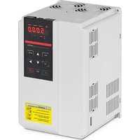
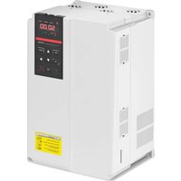
USER MANUAL FI-11000 MSW
natural_image
Technical line drawing of a rectangular enclosure or enclosure with dimensions labeled D and H (no text or symbols beyond labels)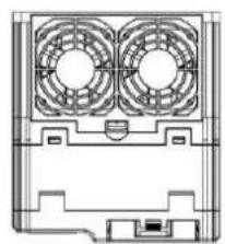
natural_image
Technical line drawing of a dual fan assembly (no text or symbols)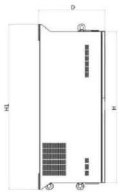
natural_image
Technical line drawing of a rectangular enclosure or enclosure with dimensions labeled H1 and D, showing internal layout and mounting points (no text or symbols beyond labels)Gehäusemontage
natural_image
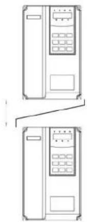
Line drawing of two identical rectangular electronic devices with control panels and indicator lights (no text or symbols)natural_image
Technical line drawing of a multi-level industrial machine or server unit (no text or symbols visible)Figure 3-7 Wiring diagram of analog input terminal

Figure 3-8 Treatment wiring diagram of analog input terminal
line
| Frequency (%) | Spannung Vb in %. | |---|---| | 0 | V1 | | F2 | V2 | | F3 | V3 | | Fb | V3 |flowchart
graph TD
    A["SB2"] --> B["DI1"]
    C["SB1"] --> D["DI3 Three line operation control"]
    E["SB3"] --> F["DI2 Reverse run (REV)"]
    G["COM Digital public end"] --> H["Forward running (FWD)"]
line
| Panel | Frequency (0mA) | Earnings (%) | |-------|-----------------|--------------| | Top | 0 | 100.0 | | Top | 10 | 100.0 | | Bottom | 0 | -100.0 | | Bottom | 10 | 100.0 |line
| Time t | Output frequency Hz | Output voltage effective value | Halt DC braking amount | Run command | | ------ | ------------------- | ------------------------------ | ----------------------- | ----------- | | 0 | 0 | 0 | 0 | 0 | | 1 | 1 | 1 | 0 | 0 | | 2 | 1 | 1 | 0 | 0 | | 3 | 1 | 1 | 0 | 0 | | 4 | 1 | 1 | 0 | 0 | | 5 | 1 | 1 | 0 | 0 | | 6 | 1 | 1 | 0 | 0 | | 7 | 1 | 1 | 0 | 0 | | 8 | 1 | 1 | 0 | 0 | | 9 | 1 | 1 | 0 | 0 | | 10 | 1 | 1 | 0 | 0 | | 11 | 1 | 1 | 0 | 0 | | 12 | 1 | 1 | 0 | 0 | | 13 | 1 | 1 | 0 | 0 | | 14 | 1 | 1 | 0 | 0 | | 15 | 1 | 1 | 0 | 0 | | 16 | 1 | 1 | 0 | 0 | | 17 | 1 | 1 | 0 | 0 | | 18 | 1 | 1 | 0 | 0 | | 19 | 1 | 1 | 0 | 0 | | 20 | 1 | 1 | 0 | 0 | | 21 | 1 | 1 | 0 | 0 | | 22 | 1 | 1 | 0 | 0 | | 23 | 1 | 1 | 0 | 0 | | 24 | 1 | 1 | 0 | 0 | | 25 | 1 | 1 | 0 | 0 | | 26 | 1 | 1 | 0 | 0 | | 27 | 1 | 1 | 0 | 0 | | 28 | 1 | 1 | 0 | 0 | | 29 | 1 | 1 | 0 | 0 | | 30 | 1 | 1 | 0 | 0 | | Note: The output frequency Hz and output voltage effective value are estimated based on the simulation parameters. The Halt DC braking amount and halt duration are indicated at key time points. The Halt DC braking time is marked as 'Halt DC braking waiting time'. The 'Run command' indicates the run command.| P7-03 | LED display running parameters 1 | Factory default | 1F | ||
| Setting range | 0000~FFFF |  | Running frequency 1 (Hz)Set frequency (Hz)Bus voltage (V)Output voltage (V)Output current (A)Output power (kW)Output torque (%)DI input status (V)DO output statusAI1 voltage (V)AI2 voltage (V)AI3 voltage (V)Count valueLength valueLoad speed displayPID settingIf a parameter needs to be displayed during the running, set the corresponding bit to 1, and set P7-0 3 to the hexadecimal equivalent of this binary number. | ||
| P7-04 | LED display running parameters 2 | Factory default | 0 | ||
| Setting range | 0000~FFFF |  | PID feedbackPLC stagePulse setting frequency (kHz)Running frequency 2Remaining running timeAI1 voltage before correctionAI2 voltage before correctionAI3 voltage before correctionLinear speedCurrent power-on time (Hour)Current running time (Minute)Pulse setting frequency (Hz)Communication setting valueEncoder feedback speed (Hz)Main frequency X display (Hz)Auxiliary frequency Y display (Hz)If a parameter needs to be displayed during the running, set the corresponding bit to 1, and set P7-0 4 to the hexadecimal equivalent of this binary number. | ||
line
| Zeit | Ausgangsstrom | Erkennungssignal für Überschreitung des Ausgangsstroms | |------|---------------|--------------------------------------------------------| | 0 | Low | 0 | | Peak | High | 1 | | Peak 1 | Medium | 0 | | Peak 2 | Low | 0 | | Peak 3 | High | 1 | | Peak 4 | High | 1 | | Peak 5 | Medium | 0 | | Peak 6 | Low | 0 | | Peak 7 | High | 1 | | Peak 8 | High | 1 | | Peak 9 | Medium | 0 | | Peak 10| Low | 0 | | Peak 11| High | 1 | | Peak 12| High | 1 | | Peak 13| Medium | 0 | | Peak 14| Low | 0 | | Peak 15| High | 1 | | Peak 16| High | 1 | | Peak 17| Medium | 0 | | Peak 18| Low | 0 | | Peak 19| High | 1 | | Peak 20| High | 1 | | Peak 21| Medium | 0 | | Peak 22| Low | 0 | | Peak 23| High | 1 | | Peak 24| High | 1 | | Peak 25| Medium | 0 | | Peak 26| Low | 0 | | Peak 27| High | 1 | | Peak 28| High | 1 | | Peak 29| Medium | 0 | | Peak 30| Low | 0 | | Peak 31| High | 1 | | Peak 32| High | 1 | | Peak 33| Medium | 0 | | Peak 34| Low | 0 | | Peak 35| High | 1 | | Peak 36| High | 1 | | Peak 37| Medium | 0 | | Peak 38| Low | 0 | | Peak 39| High | 1 | | Peak 40| High | 1 | | Peak 41| Medium | 0 | | Peak 42| Low | 0 | | Peak 43| High | 1 | | Peak 44| High | 1 | | Peak 45| Medium | 0 | | Peak 46| Low | 0 | | Peak 47| High | 1 | | Peak 48| High | 1 | | Peak 49| Medium | 0 | | Peak 50| Low | 0 | | Peak 51| High | 1 | | Peak 52| High | 1 | | Peak 53| Medium | 0 | | Peak 54| Low | 0 | | Peak 55| High | 1 | | Peak 56| High | 1 | | Peak 57| Medium | 0 | | Peak 58| Low | 0 | | Peak 59| High | 1 | | Peak 60| High | 1 | | Peak 61| Medium | 0 | | Peak 62| Low | 0 | | Peak 63| High | 1 | | Peak 64| High | 1 | | Peak 65| Medium | 0 | | Peak 66| Low | 0 | | Peak 67| High | 1 | | Peak 68| High | 1 | | Peak 69| Medium | 0 | | Peak 70| Low | 0 | | Peak 71| High | 1 | | Peak 72| High | 1 | | Peak 73| Medium | 0 | | Peak 74| Low | 0 | | Peak 75| High | 1 | | Peak 76| High | 1 | | Peak 77| Medium | 0 | | Peak 78| Low | 0 | | Peak 79| High | 1 | | Peak 80| High | 1 | | Peak 81| Medium | 0 | | Peak 82| Low | 0 | | Peak 83| High | 1 | | Peak 84| High | 1 | | Peak 85| Medium | 0 | | Peak 86| Low | 0 | | Peak 87| High | 1 | | Peak 88| High | 1 | | Peak 89| Medium | 0 | | Peak 90| Low | 0 | | Peak 91| High | 1 | | Peak 92| High | 1 | | Peak 93| Medium | 0 | | Peak 94| Low | 0 | | Peak 95| High | 1 | | Peak 96| High | 1 | | Peak 97| Medium | 0 | | Peak 98| Low | 0 | | Peak 99| High | 1 | | End | - | - |line
| PID-Abweichung | Parametr PID | |---|---| | PA-05, PA-06, PA-07 | 1 | | PA-19 | 1 | | PA-20 | 1 | | PA-15, PA-16, PA-17 | 1 |natural_image
Technical line drawing of an internal electronic device casing with ventilation grilles and mounting brackets (no text or symbols)natural_image
Isometric technical line drawing of a server or chassis unit with internal components and mounting bracket (no text or symbols)natural_image
Technical line drawing of an electronic device chassis with mounting brackets and ventilation slots (no text or symbols)General functions and descriptions of frequency convertor:
1) Abundant voltage classes: support three voltage classes, namely single-phase 220V, three-phase 220V and three-phase 380V.
2) Abundant control mode: apart from vector control of velocity sensor, sensorless vector control and V/F control, support V/F separation control.
3) Abundant field bus: support Modbus-RTU and CANlink field bus.
4) Abundant encoder types: support difference encoder, open collector encoder and rotary transformer, etc.
5) Brand-new sensorless vector control algorithm
Brand-new SVC creates better low-velocity stability, stronger low-frequency load capacity, and supports torque control of SVC.
6) Powerful background software: uploading, downloading parameters, real-time oscilloscope can be realized on background software.
| Functions Descriptions | |
| Overheat protection of motor | After choosing PC1 expansion card, AI3 can receive temperature sensor input of motor (PT100, PT1000) to realize overheat protection |
| Fast current limiting | Avoid over-current fault of frequency convertor |
| Dual motor switch | Two sets of motor parameters can realize dual motor switch |
| Restore user parameters | Users can save or restore own parameter settings |
| Accurate AIAO | After factory calibration (or spot calibration), AIAO accuracy can be<20mv |
| Show customized parameters | Users can customize function parameters to be displayed |
| Show altered parameters | User can view function parameters after modification |
| Optional fault handing ways | Users can select action modes of convertor after confirming certain faults: free halting, deceleration halting, continual operation. The users can also select frequency for continual operation. |
| PID parameter switch | Two sets of PID parameters can switch by terminal or based on deviation |
| PID feedback loss detection | PID feedback loss detection value realizes protection during PID operation |
| DIDO positive/negative logic | Users can set positive/negative logic of DIDO |
| DIDO response delay | Users can set response delay time of DIDO |
| Run under instantaneous stop | Frequency convertor continues running within short time if instantaneous power outage or voltage decrease |
| Timing operation | Support timing operation for 6,500 minutes at most |
Opening for inspection:
When opening the box, please carefully confirm if the nameplate model and rated value of frequency convertor are consistent with order. The package contains ordered machine, qualification certificate, operation manual and warranty bill.
If any damage during transportation or certain omission, please contact with our company or supplier.
Chapter 1 Safety information and precautions
Safety definition: safety precautions are divided into two categories in the manual:

Danger: serious injury and death may occur due to operation against requirements;

Caution: moderate or minor injury, equipment damage may occur due to operation against requirements;
Please read this chapter carefully when installing, debugging and maintaining the system, and operate as per safety precautions. The company will not be liable for any injury and loss caused by operation against requirements.
1.1 Safety issues
1.1.1 Before installation:

Danger
- If any water in system, lack or damage of component when opening box, please do not install!
- If any unconformity between packing list and actual object, please do not install!

Danger
- Please move the equipment gently, otherwise it may be damaged!
- If any damaged driver or frequency convertor missing parts, please do not use! There's risk of injury!
- Do not touch components of control system with hands, otherwise there's danger of static electricity!
1.1.2 During installation:

Danger
● Install on flame retardant objects like metal and keep away from combustible, otherwise fire may occur
- Do not screw fixed bolts of components at random especially those with red marking!

Caution
- Do not put wire head or bolt in driver, otherwise the driver may be damaged!
- Please install the driver in place with little vibration and keep out of the sun.
- When above two frequency converters are put in the same cabinet, please pay attention to installation position to ensure heat dissipation effect.
1.1.3 During wiring:

Danger
- Please observe the manual guidance and construct by professional electric engineering staff, otherwise danger may occur!
● Breaker should separate frequency convertor and power, otherwise fire may occur! - Please ensure that power is at zero-energy state before wiring, otherwise electric shock may occur!
- Please keep correct earthing of convertor as per standards, otherwise electric shock may occur!

Danger
- Do not connect input power to output terminal (U, V, W) on frequency convertor. Pay attention to marking on wiring terminal and do not wire wrongly, otherwise driver may be damaged!
- Ensure that all wirings conform to EMC requirements and regional safety standard. All wire diameters refer to suggestions in manual, otherwise accident may occur!
- Do not connect brake resistor directly between DC bus (+) (-) terminals, otherwise fire may occur!
- Encoder shall use shielded wire single and ensure reliable earthing for terminal of shielding layer!
1.1.4 Before electrifying:

Caution
- Please confirm the consistence between voltage class of input power and rated voltage class of frequency convertor; correctness of wiring positions of power input terminal (R, S, T) and output terminals (U, V, W). Check if any short circuit of peripheral circuit connecting to driver and if wiring circuit is tightened, otherwise driver may be damaged!
● Neither part of frequency convertor needs withstand voltage test as the product has been tested!

Danger
Electrify frequency convertor after covering cover plate, otherwise electric shock may occur!
- Wiring of all periphery accessories shall comply with manual guidance and keep correct wiring as per circuit connection method in manual, otherwise accident may occur!
1.1.5 After electrifying:

Danger
- Do not open cover plate after electrifying, otherwise electric shock may occur!
- Do not touch driver or peripheral circuit with wet hands, otherwise electric shock may occur!
- Do not touch any input or output terminal of frequency convertor, otherwise electric shock may occur!
- When firstly electrifying, frequency convertor will conduct security detection of external strong current loop, and do not touch U, V, W wiring terminal of driver or wiring terminal of motor, otherwise electric shock may occur!
1.1.6 During operation:

Danger
- Do not touch cooling fan or discharge resistance to feel temperature, otherwise burn may occur!
● Non-professional artisan shall not detect signal, otherwise personal injury or device damage may occur!

Caution
● Avoid things falling in device during operation of frequency convertor, otherwise damage may occur!
- Do not control driver by turning on or off contactor, otherwise damage may occur!
1.1.7 During maintenance:

Danger
- Do not repair or maintain device when electrifying, otherwise electric shock may occur!
- Only maintain and repair driver when voltage of frequency converter<DC36V since 2 minutes after outage, otherwise residual electric charge on capacitance may cause personal injury!
- Those without professional training shall not repair or maintain frequency convertor, otherwise personal injury or device damage may occur!
- Parameters shall be set after changing frequency convertor, all pluggable plugins shall be inserted and plugged after outage!
1.2 Precautions
1.2.1 Insulation inspection of motor
When firstly using motor, using motor again after putting for a long time and regularly checking motor, insulation inspection of motor is essential to prevent damaging frequency convertor due to invalid insulation of motor winding. During insulation inspection, separate motor wire from frequency convertor. 500V voltage-type tramegger is suggested and ensure measured insulation resistance≥5MΩ.
1.2.2 Thermal protection of motor
If selected motor does not match with rated capacity of frequency convertor, especially if rated power is larger than that of frequency convertor, please adjust related parameter values of motor protection or install thermal relay in front of motor for protection.
1.2.3 Operation above power frequency
The frequency convertor offers output frequency at 0Hz\~3200Hz. If users need to operate at above 50Hz, please consider the tolerance of mechanical device.
1.2.4 Vibration of mechanical device
Mechanical resonance point of load device may exist at certain output frequency of frequency convertor, and hopping frequency parameter can be set to avoid.
1.2.5 About heating and noise of motor
Output voltage of frequency convertor is PWM wave containing certain harmonic, so temperature rise, noise and vibration of motor will slightly increase when comparing with power frequency operation.
1.2.6 Voltage-sensitive parts or capacitance of improving power factor exist on output side
Output of frequency convertor is PMB wave. If capacitance of improving power factor or voltage dependent resistor for thunder prevention is installed on output side, instantaneous over current and even damage of frequency convertor can be caused easily. Please do not use.
1.2.7 Switching devices such as contactor for input and output terminals of frequency convertor
If contactor is installed between power and input terminal of frequency convertor, this contactor is not allowed to control the start and stop of frequency convertor. If this contactor is required to control the start and stop of frequency convertor, the interval should be not less than one hour. Frequent charging and discharging will easily reduce the lifespan of capacitor within frequency convertor. If switching devices such as contactor are installed between output terminal and motor, ensure the operation of frequency convertor without output, otherwise module damage may occur easily.
1.2.8 Use beyond rated voltage value
It's not suitable to use this series frequency convertor beyond operating voltage range allowed by the manual, otherwise device damage may be caused. If necessary, please use corresponding voltage boosting or dropping equipment for voltage transformation.
1.2.9 Three-phase input changes to be two-phase input
Do not change three-phase frequency convertor to be two-phase, otherwise fault or damage may occur.
1.2.10 Lightening impulse protection
There's lightening stroke over-current protection device in frequency convertor, so it has certain self-protection ability for inductive thunder. If lightening stroke is frequent in the place of client, additional protection in front of frequency convertor is essential.
1.2.11 Altitude and derating use
In the region with altitude exceeding 1,000m, the heat dissipation effect of frequency convertor weakens due to thin air, so it's necessary to derate for use. Please contact our company for consultation.
1.2.12 About adaptive motor
1) Standard adaptive motor is four-pole squirrel-cage asynchronous induction motor. If it's not above motor, please select frequency convertor as per rated current of motor.
2) Cooling fan and rotor spindle of non-variable frequency motor is coaxial connection. If rotation speed reduces, cooling effect of fan will reduce, so the occasion of overheating motor should be installed with strong exhaust fan or changed to be variable frequency motor.
3) Standard parameters of adaptive motor have been built in frequency convertor. It's necessary to identify motor parameters or modify default value based on actual situation to conform to actual value as far as possible, otherwise operation effect and protection performance may be affected.
4) Short circuit of cable or within motor can lead to alarm and even explosion of frequency convertor. Please firstly conduct insulation short-circuit test for initially installed motor and cable, and it's also essential for daily maintenance. Please completely separate frequency convertor from tested part when conducting the test.
Chapter 2 Product information
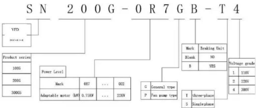
2.1 Naming rule
flowchart
graph TD
    A["SN 200G - OR7 GB - T 4"] --> B["VFD"]
    A --> C["Power Level"]
    A --> D["Mark"]
    A --> E["Adaptable motor (kW)"]
    A --> F["..."]
    A --> G["22kW"]
    A --> H["General type"]
    A --> I["P Fan pump type"]
    A --> J["S Single phase"]
    K["Mark"] --> L["Braking Unit"]
    M["Blank"] --> N["NO"]
    O["B"] --> P["YES"]
    Q["I"] --> R["three-phase"]
    S["S"] --> S1["Single phase"]
    T["Voltage grade"] --> U["1 110V"]
    T --> V["2 220V"]
    T --> W["4 380V"]
Figure 2-1 Naming specification
2.2 Nameplate
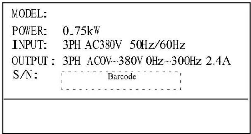
Figure 2-2 Nameplate
Figure 2-1 Model and technical data of frequency convertor
| Model of frequency convertor | Power capacity (kVA) | Input current (A) | Output current (A) | Adaptive motor | |
| kW | HP | ||||
| Three-phase power: 380V, 50/60Hz | |||||
| 10061537 | 1.5 | 3.4 | 2.1 | 0.75 | 1 |
| 10061534 | 3.0 | 5.0 | 3.8 | 1.5 | 2 |
| 10061533 | 4.0 | 5.8 | 5.1 | 2.2 | 3 |
| 10061532 | 5.9 | 10.5 | 9.0 | 3.7 | 5 |
| 10061531 | 8.9 | 14.6 | 13.0 | 5.5 | 7.5 |
| 10061530 | 11.0 | 20.5 | 17.0 | 7.5 | 10 |
| 10061536 | 17.0 | 26.0 | 25.0 | 11.0 | 15 |
| 10061535 | 21.0 | 35.0 | 32.0 | 15.0 | 20 |
2.4 Technical specifications
Figure 2-2 Technical specifications of frequency convertor
| Items | Specifications | |
| Highest frequency | Vector control: 0~300HzV/F control: 0~3200Hz | |
| Carrier frequency | 0.5kHz~16kHzAdjust carrier frequency automatically based on load characteristic | |
| Input frequency resolution | Number setting: 0.01HzSimulation setting: highest frequency ×0.025%SVCFVCV/F control | |
| Control mode | ||
| Starting torque | G-style machine: 0.5Hz/150% (SVC); 0Hz/180% (FVC)P-style machine: 0.5Hz/100% | |
| Basic functions | Speed regulation range | 1: 100 (SVC) 1: 1000 (FVC) |
| Speed stabilizing precision | ±0.5% (SVC) ±0.02% (FVC) | |
| Torque control precision | ±5% (FVC) | |
| Overload capacity | G-style machine: 150% rated current at 60s; 180% rated current at 3sP-style machine: 120% rated current at 60s; 150% rated current at 3s | |
| Torque promotion | Automatic torque promotion; manual torque promotes by 0.1%~30.0% | |
| V/F curve | Three ways: linear type; multipoint type; N^th power type V/F curve(1.2 power, 1.4 power, 1.6 power, 1.8 power, 2 power) | |
| V/F separation | 2 ways: full separation, semi-separation | |
| Acceleration/deceleration curves | Linear or S-curve acceleration/deceleration way.Four kinds of acceleration/deceleration timeAcceleration/deceleration time range: 0.0~6500.0s | |
| DC braking | DC braking frequency: 0.00Hz~maximum frequency; Braking time:0.0s~36.0s braking action; Current value: 0.0%~100.0% | |
| Inching control | Inching frequency range: 0.00Hz~50.00Hz;Inching acceleration/deceleration time 0.0s~6500.0s | |
| Simple PLC, multi-stage velocity operation | Realize 16-stage velocity operation at most through built-in PLC or control terminal | |
| Built-in PID | Easy to realize process control, closed-loop control system | |
| Automatic voltage regulation | Keep constant output voltage automatically if any change of network voltage | |
| Overvoltage, overcurrent, stalling control | Limit current/voltage automatically during operation, prevent frequent tripping caused by over-current and over-voltage | |
| Fast current-limiting function | Reduce over-current fault, protect normal operation of convertor | |
| Torque limit and control | “Nawy” character limit torque during operation,prevent frequent overcurrent tripping, closed-loop vector mode can realize torque control | |
| Items Specifications | ||
| Individualized functions | Excellent performance | Realize motor control with high-performance current vector control |
| Operate under instantaneous stop | Offset reduced voltage through load feedback energy if instantaneous outage, keep continual operation of frequency convertor within short time | |
| Fast current limiting | Avoid frequent over-current fault of frequency convertor | |
| Timing control | Timing control function: set time range 0.0Min~6500.0Min | |
| Multi-motor switch | 2 sets of motor parameters realize switch control of 2 motors | |
| Multi-threading bus | Support two kinds of spot field bus: R S -4 8 5 , C A N li n k | |
| Overheating protection | Optional multi-function card, analog input A13 can receive motor temperature sensor input (PT100, PT1000) | |
| Multi encoder | Support various encoders such as differentiation, open collector and rotary transformer | |
| Programmable by users | Optional user programmable card realizes secondary development | |
| Powerful background software | Support parameter operation and virtual oscilloscope function. Realize graphic monitoring of internal status of frequency convertor through virtual oscilloscope | |
| Operation | Command source | Given operation panel, given control terminal, given serial communication port. Switch through multiple ways |
| Frequency source | 10 frequency sources: given digit, given analog voltage, given analog current, given pulse, given serial port. Switch through multiple ways | |
| Auxiliary frequency source | 10 auxiliary frequency sources. Realize auxiliary frequency trimming and frequency synthesis flexibly | |
| Input terminals | Standard:5 digital input terminals, in which 1 terminal supports high-speed impulse input at100Hz2 analog input terminals, in which 1 supports voltage input at 0~10V, 1 supports voltage support at 0~10V or current input at 4~20mAExpansion capability:5 digital input terminals1 analog input terminal supports voltage support at 0~10V | |
| Output terminals | Standard:1 high-speed pulse output terminal (open collector is optional), support square signal output at 0~100kHz1 digital output terminal1 relay output terminal1 analog output terminal supports current input at 0~20mA or voltage support at 0~10VExpansion capability:1 digital output terminal1 relay output terminal1 analog output terminal supports current input at 0~20mA or voltage support at 0~10V | |
| Display and keyboard operation | LED display | Display parameters |
| Key locking and function selection | Partial or all locking of keys, define function range of some keys to prevent misoperation | |
| Protection function | Short-circuit detection of motor when electrifying, input/output default phase protection, over-current protection, overvoltage protection, undervoltage protection, overheating protection, overload protection | |
| Optional accessories | LCD operation panel, braking unit, multi-function expansion card, IO expansion card, RS485 communication card, CANlink communication card, differential input PG card, rotary transformer PG card, OC input PG card | |
| Operating environment | Using place | Indoor without direct sunlight, dust, corrosive gas, combustible gas, oil mist, water vapor, dropping water or salinity |
| Altitude | < 1,000m | |
| Environment temperature | -10°C~+40°C (environment temperature at 40°C~50°C, please derate to use | |
| Humidity | < 95%RH, no condensing drops | |
| Virbration | < 5.9m/s (0.6g) | |
| Storage temperature | -20°C~+60°C | |
2.5 Outside drawing
mounting hole dimension
2.5.1 Outside drawing
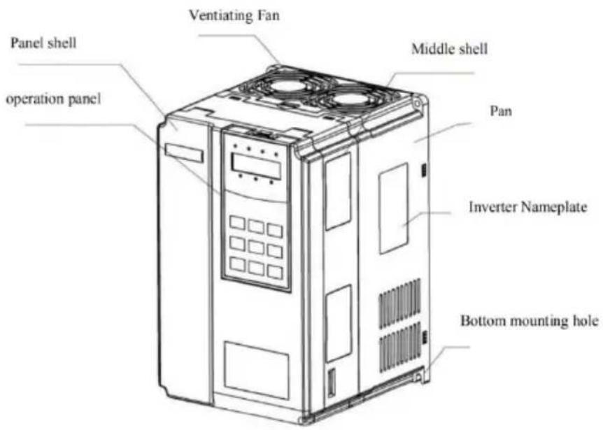
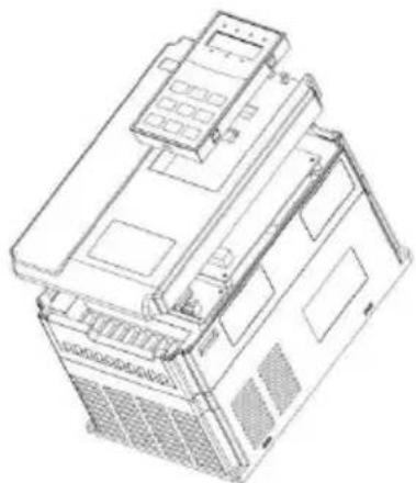
Figure 2-3 Outside drawing of VFD
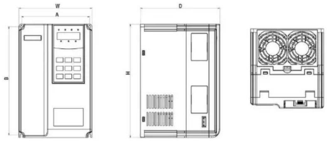
Figure 2-4 Schematic diagram of external dimension and mounting dimension of plastic structure
natural_image
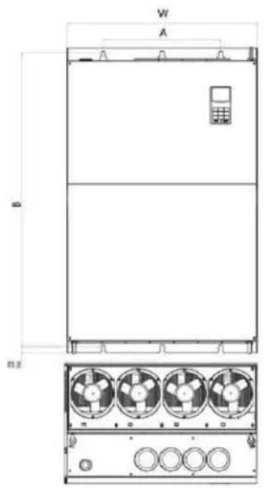
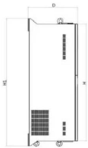
Technical line drawing of a rectangular enclosure or storage unit with labeled dimensions H, D, and H1 (no text or symbols beyond labels)Figure 2-5 Schematic diagram of external dimension and mounting dimension of metal plate structure
Shell structures of models are as follow:
| Model Shell type | |
| Single-phase 220V | |
| 0.4kW~2.2kW | Plastic structure |
| Three-phase 220V | |
| 0.4kW~7.5kW | Plastic structure |
| 11kW~75kW | Metal plate structure |
| Three-phase 380V | |
| 0.75kW~15kW | Plastic structure |
| 18.5kW~400kW | Metal plate structure |
5.5.2 Outside drawing and mounting hole dimension (mm) of frequency convertor Figure 2-3
Outside drawing and mounting hole dimension
| Model of frequency converter | Mounting hole (mm) External Dimension (mm) | Hole diameter | Weight (kg) | ||||
| A B H | W D | ||||||
| 10061537 | 114 | 172 | 186 | 125 | 159 | 5.0 | 1.7 |
| 10061534 | |||||||
| 10061533 | |||||||
| 10061532 | 149 | 237 | 218 | 160 | 174 | 5.0 | 3.2 |
| 10061531 | |||||||
| 10061530 | |||||||
| 10061536 | 190 | 305 | 322 | 208 | 192 | 6.0 | 6.5 |
| 10061535 | |||||||
2.5.3 External dimension of display panel
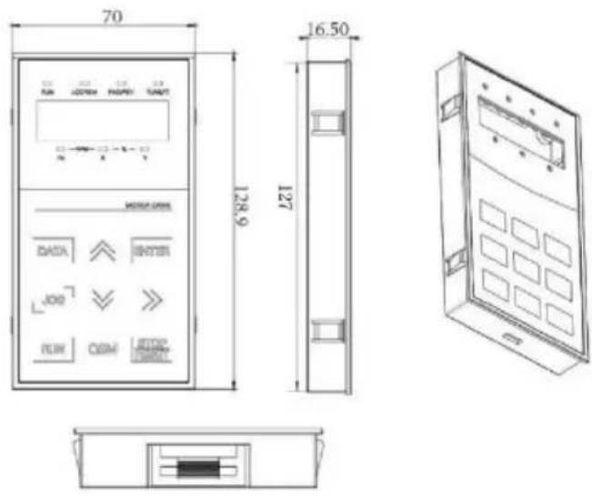
Figure 2-6 External dimension of display panel
Hole size of display panel:

Figure 2-7 Hole size of display panel
2.5.4 Dimensional drawing of external DC reactor
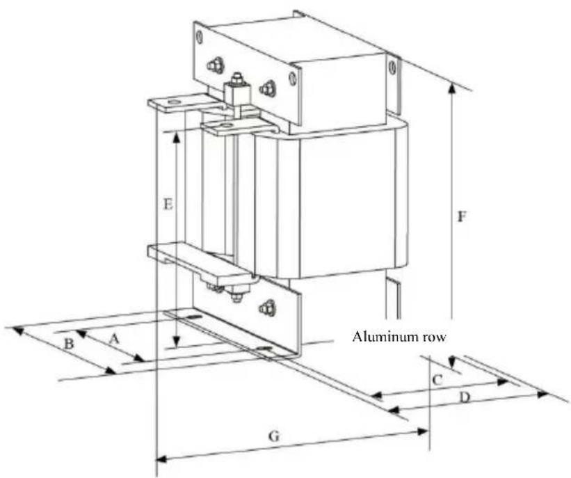
Figure 2-8 Dimensional drawing of external DC reactor
Note: non-standard ones can be customized if any special requirements
Installation way of external DC reactor: when installing frequency convertor, users need to remove the short-circuit copper bar between wiring terminal P1 and (+) of major loop, connect DC reactor between P1 and (+), keep no polarity of wiring between reactor terminal and convetor terminal P1, (+). After installing DC reactor, short-circuit copper bar between P1 and (+) is not necessary.
2.6 Optional accessories
Table 2-6 Accessories of frequency convertor
| Name | Model | Function | Remark |
| External brake unit | SNBU | 18.5kW and above external brake unit | 75kW and above adopts multi-parallel connection |
| Multifunction expansion card | IO-MINI-V03 | It can add five figures input and one analog voltage input. AI3 is isolate analog quantity that can connects with PT100 and PT1000; one relay output, one figure output and one analog voltage output with RS485 / CAN | Suitable for models of 3.7KW and above |
| I/O expansion card IO1 | It can add three figures input | Suitable for whole series | |
| MODBUS communication card | RS485 | With isolating RS-485 communication card | Suitable for whole series |
| CANlink communication expansion card | CANLINK-V03 | CANlink communication adapter card | Suitable for whole series |
| Interface card of differential encoder | PG1 | Interface card of differential rotary encoder, adaptive for 5V power source | Suitable for whole series |
| Interface card of rotary transformer | PG2 | Suitable for rotating encoder, driving frequency 10kHz, DB9 interface | Suitable for whole series |
| Interface card of open collector encoder | PG3 | Interface card of open collector encoder, with 1: 1 frequency dividing output, adaptive for 15V power source | Suitable for whole series |
| Introduced LED operating panel | SNKE | Introduced LED display and operating keyboard | Suitable for SN series |
| Extension cable | SNCAB | Introduced extension cable | Standard configuration 3 meter |
2.7 Routine maintenance of frequency convertor
2.7.1 Routine maintenance
The influence of environment temperature, humidity, dust and vibration will lead to aging of internal components and potential fault, or reduce lifespan of frequency convertor, so it's necessary to conduct routine and regular maintenance.
Routine inspection items:
1) If any abnormal change of sound during motor operation
2) If any vibration during motor operation
3) If any change of installing environment for frequency convertor
4) If normal work of cooling fan for frequency convertor
5) If overheating of frequency convertor
2.7.2 Regular inspection
Regular inspection items:
1) Inspect air channel and clean regularly
2) Inspect if any loosening of screw
3) Inspect if any arc trace of wiring terminal
2.7.3 Storage of frequency convertor
After purchasing frequency convertor, users should pay attention to temporary and long-term storage:
- Put in packaging box of our company as per original package for storage.
- Long-term storage will lead to deterioration of electrolytic capacitor. Ensure electrifying once for at
least 5 hours within 2 years, and voltage regulator should be used to gradually increase input voltage to rated value.
2.8 Warranty
Free maintenance only suit to frequency convertor. If any fault or damage under normal use, our company is liable for maintenance for 18 months (since the date of leaving factory and barcode on machine prevails). If beyond 18 months, rational maintenance fee will be charged. Under below conditions, certain maintenance fee will be charged within 18 months: device damage caused by violating stipulations in manual; damage caused by fire, flood and abnormal voltage, etc; damage caused by using frequency convertor for abnormal functions. Related service fee will be calculated as per unified standard of manufacturer. If any contract, the contract will prevail.
2.9 Model selection guidance of braking parts
Figure 2-7 is guidance data. Users can select different resistance value and power based on actual situation (but resistance value should not be lower than recommended value in figure, the power can be large). The selection of braking resistance depends on motor power in actual application system, and it's related to system inertia, deceleration time, potential energy load, so uses can select based on actual situation. The larger the system inertia, the shorter the deceleration time and three frequency the braking will be, so braking resistance should select large power and little resistance value.
2.9.1 Selection of resistancevalue
During braking, regenerated energy of motor is almost fully consumed on braking resistance. Formula is below: U*U/R=Pb
U----braking voltage of stable braking (vary with different systems, generally 700V for 380VAC) Pb----braking power
2.9.2 Power selection of braking resistance
In theory, power of braking resistance conforms with braking power.
Derating to 70% can be used.
Formula: 0.7Pr=PbD
Pr----power of resistance; D----braking frequency (proportion in whole process during regeneration)
Uncoil/Coil ----20 \~30%
Centrifuge----50%\~60%
Casual braking load----5%
10% in general
Figure 2-7 Model selection of braking parts
| Model of frequency convertor | Recommended power | Recommended resistance value | Braking unit | Note |
| 10061537 | 150W | ≥300Ω | Standard built-in | No special instructions |
| 10061534 | 150W | ≥220Ω | ||
| 10061533 | 250W | ≥200Ω | ||
| 10061532 | 300W | ≥130Ω | ||
| 10061531 | 400W | ≥90Ω | ||
| 10061530 | 500W | ≥65Ω | ||
| 10061536 | 800W | ≥43Ω | ||
| 10061535 | 1000W | ≥32Ω |
Chapter 3 Mechanical and electrical installation
3.1 Mechanical installation
3.1.1 Installation environment:
1) Environment temperature: ambient environment temperature has great influence on lifespan of frequency convertor, so operating ambient temperature of frequency convertor is not allowed to exceed temperature range (-10°C\~50°C).
2) Put frequency convertor on surface of flame retardant object and leave enough space for heat dissipation around. Large heat produces when the frequency convertor operates. Besides, install vertically on installation support with screw.
3) Install in the place with little vibration. Vibration shall be < 0.6G. Keep away from punch.
4) Avoid installing in the place with direct sunlight, humidity and dropping water, etc.
5) Avoid installing in the oaccasions with corrosive, inflammable and explosive gas in the air.
6) Avoid installing in the place with oil stain, dust and metal dust.
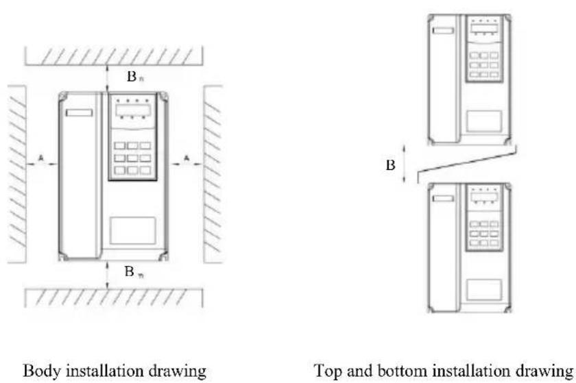
Figure 3-1 Installation diagram of frequency convertor
Body installation: A dimension can not be considered if power of frequency convertor is ≤22kW . A shall be >50mm if power of frequency convertor is >22kW.
Top and bottom installation: please install thermal insulation guide plate as per drawing.
| Power grade | Installation dimension | |
| B | A | |
| ≤15kW ≥100mm | No requirements | |
| 18.5kW—30kW | ≥200mm | ≥50mm |
| ≥37kW ≥300mm | ≥50mm | |
3.1.2 Heat dissipation should be noticed for mechanical installation. Please pay attention to bellows:
1) Install frequency convertor vertically so that heat can dissipate upward, prohibit inverting. If there are multiple frequency converters in cabinet, abreast installation is suggested. For the occasions requiring top and bottom installation, install thermal insulation guide plate as per drawing 3-1.
2) Installation space follows by drawing 3-1 to ensure heat dissipation space of frequency convertor. Consider heat dissipation situation of other components within cabinet.
3) Installation bracket shall be flame retardant material.
4) For the occasion with metal dust, suggest installing radiator outside cabinet. The space of full sealing cabinet should be as large as possible.
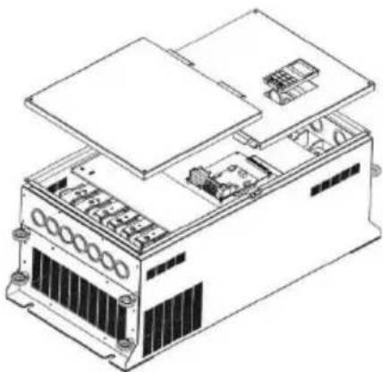
3.1.3 Disassembly and installation of lower cover plate
Frequency convertor <18.5kW adopts plastic shell. The disassembly of lower cover plate of plastic shell refers to figure 3-2, 3-3. Push out hook of lower cover plate from inside with tool.
natural_image
Line drawing of a multi-tiered industrial machine or server unit (no text or symbols visible)Figure 3-2 Disassembly drawing of lower cover plate of plastic shell
natural_image
Technical line drawing of an electronic device with internal components and mounting holes (no text or symbols)Figure 3-3 Disassembly drawing of lower cover plate of metal plate shell
Frequency convertor >18.5kW adopts metal plate shell. The disassembly of lower cover plate of metal plate shell refers to figure 3-3. Unscrew the screw on lower cover plate directly with tool.
| Danger |
| ● When disassembling lower cover plate, avoid falling plate from injury to device and body |
3.2 Electrical installation
3.2.1 Model selection guidance of periphery electrical components
Figure 3-1 Model selection guidance of periphery electrical components for frequency convertor
| Model of frequency convertor | (MCCB) A | Recommend contactor A | Major loop wiring on input side mm^2 | Major loop wiring on output side mm^2 | Recommend control loop wiring mm^2 |
| Three-phase380V | |||||
| 10061537 | 10 | 10 | 2.5 | 2.5 | 1.0 |
| 10061534 | 16 | 10 | 2.5 | 2.5 | 1.0 |
| 10061533 | 16 | 10 | 2.5 | 2.5 | 1.0 |
| 10061532 | 25 | 16 | 4.0 | 4.0 | 1.0 |
| 10061531 | 32 | 25 | 4.0 | 4.0 | 1.0 |
| 10061530 | 40 | 32 | 4.0 | 4.0 | 1.0 |
| 10061536 | 63 | 40 | 4.0 | 4.0 | 1.0 |
| 10061535 | 63 | 40 | 6.0 | 6.0 | 1.0 |
3.2.2 Instructions of peripheral electrical components
Figure 3-2 Instructions of peripheral electrical components for frequency convertor
| Part name | Installing Functional description | |
| Air switch | Front of input circuit | Break power if any overcurrent of downstream equipment |
| Contactor | Input side of air switch and convertor | Turn on/off power of convertor. Avoid frequent on/off operation of convertor through contactor (< twice every minute) or starting operation directly |
| AC input reactor | Input side of convertor | Promote power factor on input side; eliminate higher harmonic on input side and prevent device damage caused by voltage waveform distortion; eliminate unbalanced input current caused by unbalance between power phase |
| EMC input filter | Input side of convertor | Reduce external conduction and radiated interference of convertor; reduce conduction interference from power end to convertor, promote antijamming capability of convertor |
| DC reactor | DC bus side of convertor | Promote power factor on input side; enhance efficiency and heat stability of convertor. Eliminate influence of higher harmonic on input side on convertor, reduce external conduction and radiated interference |
| AC output reactor | Between output side of convertor and motor. Install near frequency convertor | Output side of convertor contains much higher harmonic. If motor is far away from convertor, much distributed capacitance exists in circuit. Certain harmonic may produce resonance in circuit, which will damage insulating property of motor and even motor, produce large leak current and cause frequent protection of convertor. The distance between convertor and motor generall exceeds 50m, suggest installing output AC reactor |
3.2.3 Wiring way
Wiring diagram of frequency convertor:
flowchart
graph TD
    A["Three-phase380V Input power 50/60Hz"] --> B["MCCB"]
    B --> C["R S"]
    C --> D["External reactor"]
    D --> E["MDBU55"]
    E --> F["Brake unit"]
    F --> G["(-)"]
    G --> H["U"]
    H --> I["M"]
    I --> J["Keyboard port"]
    J --> K["J7"]
    K --> L["PG card port"]
    L --> M["Multi-function expansion card port"]
    M --> N["J3"]
    N --> O["J12"]
    O --> P["AOI"]
    P --> Q["GND"]
    Q --> R["FM"]
    R --> S["Open collector 1 (impulse output 1)"]
    S --> T["CME DO1"]
    T --> U["Open collector 2"]
    U --> V["CME"]
    V --> W["T/C"]
    W --> X["T/B"]
    X --> Y["T/A"]
    Y --> Z["Fault contact output AC 250V 10mA~3A DC 30V 10mA~1A"]
    A --> AA["OP OP COM 24V"]
    AA --> AB["+24V DI1"]
    AB --> AC["DI2"]
    AC --> AD["DI3"]
    AD --> AE["DI4"]
    AE --> AF["DI5"]
    AF --> AG["COM"]
    AG --> AH["10V Power for frequency setting +10V 10 mA"]
    AH --> AI["AI1 Analog input"]
    AI --> AJ["AI2 Analog input 2"]
    AJ --> AK["GND"]
    AK --> AL["PE (connect shells) 14"]
    AL --> AM["COM"]
Figure 3-4 Wiring diagram of frequency convertor
Precautions:
1) ◎ refers to terminal of major loop, ○ refers to terminal of control loop.
2) Brake resistance needs to be selected based on user demands, see more details in model selection guidance of brake resistance.
3.2.4 Terimal and wiring of main circuit
1) Description of terminal of main circuit for single-phase frequency converter
| Terminal marking | Name | Description |
| L1, L2 | Input terminal of single-phase power | Contact poin of single-phase 220V AC power |
| (+), (-) | Positive/negative terminals of DC bus | Input point of DC bus |
| (+), PB | Connection terminal of brake resistance | Connect brake resistance |
| U, V, W | Output terminal of convertor | Connect three-phase motor |
| PE\ | Earthing terminal | Earthing terminal |
2) Description of terminal of main circuit for single-phase frequency convertor
| Terminal marking | Name | Description |
| R、S、T | Input terminal of three-phase power | Connection point of AC input three-phase power |
| (+), (-) | Positive/negative terminals of DC bus | Input point of DC bus and brake unit |
| (+), PB | Connection terminal of brake resistance | Connect brake resistance |
| P1, (+) | Connection terminal of external DC reactor | Connection point of external DC reactor |
| U, V, W | Output terminal of convertor | Connect three-phase motor |
| PE\ | Earthing terminal | Earthing terminal |
Wiring precautions:
a) Input power L1, L2 or R, S, T:
b) Wiring on input side of convertor has no requirement on phase sequence. Wiring precautions:
1: (+) (-) terminals of DC bus: there's residual voltage for DC bus (+) (-) immediately after outage. Contact after CHARGE light extinguishes and confirm it's <36V, otherwise there is risk of electric shock.
2: When selecting external braking component, avoid inverse connection of (+) (-) polarity, otherwise it will lead to damage of frequency convertor and even fire.
3: Wiring length of brake unit should not exceed 10m. Twisted pair or tight double-line should be used for parallel wiring. Do not connect brake resistance directly to DC bus, otherwise it will lead to damage of frequency convertor and even fire.
c) Connection terminal (+), PB of brake resistance:
Confirm the model of built-in brake unit, and connection terminal of brake resistance is valid.
Model selection of brake resistance refers to recommended value and wiring distance should be <5m, otherwise frequency convertor may be damaged.
d) Connection terminal P1, (+) of external DC reactor
For the frequency convertor at above 220V37KW and 380V75kW, connection strap between P1 and (+) terminals needs to be removed when installing DC reactor externally, and connect DC reactor between two terminals.
e) U, V, W on output side of frequency convertor: output side of frequency convertor shall not connect capacitor or surge absorber, otherwise it will lead to frequent protection and even damage of convertor. Due to influence of distributed capacitance, if motor cable is too long, electric resonance will produce easily, which will damage motor insulation or produce large leak current and frequent protection of convertor. If motor cable is >100m, AC input reactor should be installed.
f) Earthing terminal PE
For different models, the marking of earthing terminal may be different, but the meaning is same. In above descriptions, means that earthing marking is PE or .
Keep reliable earthing of earthing terminal and resistance value of ground wire should be <0.1 , otherwise it will lead to abnormal operation and even damage of device. Do not use earthing terminal PE or 12 and N terminal on null line of power in common.
3.2.5 Control terminal and wiring
1) Layout diagram of terminals on control circuit is as below:
(Note: there's no short-circuit strap between CME and COM, OP and +24V of frequency convertor. Users select wiring way of CME and OP respectively through J10, J9)
| +10V | AI1 | AI2 | DI1 | DI2 | DI3 | DI4 | DI5 | COM | ||||
| GND | GND | AO1 | CME | COM | DO1 | FM | +24V | OP | T/A | T/B | T/C | |
Figure 3-5 Layout diagram of terminals on control circuit
2) Functional descriptions of control terminals
Figure 3-3 Functional descriptions of control terminals of frequency converter
| Type | Terminal symbol | Terminal name | Functional description |
| Power | +10V-GND | Connect + 10V power externally | Offer +10V power externally, max. output current: 10mABe commonly used as working power of external potentiometer, resistance value range of potentiometer. 1kΩ~5kΩ |
| +24V-COM | Connect + 24V power externally | Offer +24V power externally, be used as working power of digital input/output terminal and power of external sensorMax. output current: 200mA | |
| OP | Input terminal of external power | Connect +24V or COM through J9 jumper on control panel.If using external signal to drive DI1~DI5, OP needs to connect with external power, and pull out J9 jumper | |
| Analog input | AI1-GND | Analog input terminal 1 | 1. Range of input voltage: DC 0V~10V2. Input impedance: 22kΩ |
| AI2-GND | Analog input terminal 2 | 1. Input range: DC 0V~10V/4mA~20mA, depend on J8 jumper on control panel2. Input impedance: 22kΩ for voltage input, 500Ω for current input | |
| Digital input | DI1- OP | Digital input 1 | 1. Optical coupling isolation, be compatible with bipolar input2. Input impedance: 2.4kΩ3. Voltage range for level input: 9V~30V |
| DI2- OP | Digital input 2 | ||
| DI3- OP | Digital input 3 | ||
| DI4- OP | Digital input 4 | ||
| DI5- OP | High-speed impulse input terminal | Apart from features of DI1~DI4, it can be high-speed impulse input channel. Max. input frequency: 100kHz | |
| Analog output | AO1-GND | Analog output 1 | J5 jumper on control panel decides voltage or current output.Output voltage range: 0V~10VOutput current range:0mA~20mA |
| Digital output | DO1-CME | Digital output 1 | Optical coupling isolation, bipolar open collector outputOutput voltage range: 0V~24V; output current range: 0mA~50mACaution: digital output CME and digital input COM are internally isolated, but short circuit of CME and COM is realized through J10 jumper on control panel (DO1 is +24V drive by default). If DO1 needs to be driven by external power, pull out J10 jumper |
| FM- CME | High-speed impulse output | Be restricted by function code F5-00 “output way selection of FM terminal”As high-speed impulse output, max. frequency is 100kHzAs open-collector output, it’s the same with DO1 specification | |
| Relay output | T/A-T/B | Normally closed terminal | Drive capability of contact:AC250V, 3A, COSø=0.4DC 30V, 1A |
| T/A-T/C | Normally open terminal |
3) Functional description of jumper and auxiliary terminals
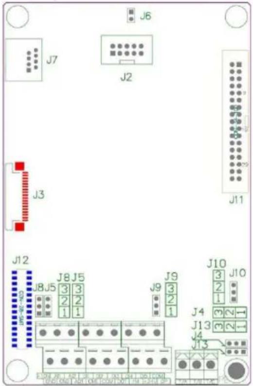
Figure 3-6 Location diagram of jumper and auxiliary terminals
Figure 3-4 Functional description of jumper and auxiliary terminals for frequency convertor
| Jumper marking | Name | Description | |
| Auxiliary terminal | J12 | Multi-function expansion card port | 28-core terminal, connect with optional cards (I/O expansion card,PLC card, various bus cards, etc) |
| J3 | PG card port | Optional: OC, differentiation, rotary transformer, etc | |
| J7 | External keyboard port | External keyboard | |
| Jumper | J4 | Select jumper to connect PE and GND | Select if PE connects with GND. In the occasion with interference, connect PE with GND to enhance anti-interference. Connection by default. (As shown in Figure 3-6, short circuit of 1-2 is connection between PE and GND, short circuit of 2-3 is no connection between PE and GND) |
| J13 | Select jumper to connect PE and COM | Select if PE connects with COM. In the occasion with interference, connect PE with COM to enhance anti-interference. Connection by default. (As shown in Figure 3-6, short circuit of 1-2 is connection between PE and COM, short circuit of 2-3 is no connection between PE and COM) | |
| J10 | Select jumper to connect CME and COM | Select if CME connects with COM. No connection by default. (As shown in Figure 3-6, short circuit of 1-2 is connection between CME and COM, short circuit of 2-3 is no connection between CME and COM) | |
| J5 | AO1 analog output selection | Decide output type of analog output terminal AO1 is voltage or current output. Voltage output by default. (As shown in Figure 3-6, short circuit of 1-2 is voltage output, short circuit of 2-3 is current output)Output voltage range: 0V-10VOutput current range: 0mA -20mA | |
| J8 | AI2 analog input selection | Decide input type of analog input terminal AO1 is voltage or current input. Voltage input by default. (As shown in Figure 3-6, short circuit of 1-2 is voltage input, short circuit of 2-3 is current input)Input voltage range: DC 0V-10VInput current range: 0mA -20mA | |
| J9 | Connection selection of OP terminal | OP terminal connects +24V or COM through J9 jumper. +24V connection by default. (As shown in Figure 3-6, short circuit of 1-2 is OP and +24V connection, short circuit of 2-3 is OP and COM connection)If using external signal to drive DI1~DI5, OP needs to connect with external power, and pull out J9 jumper | |
4) Wiring description of control terminals
a) Analog input terminal:
Due to weak analog voltage signal, it's easily influenced by external interference, shield cable is commonly used and wiring distance is as short as possible, which should not exceed 20m as shown in Figure 3-7. In the occasion where certain analog signal is seriously interfered, the side of analog signal source should be installed with filter capacitor or ferrite core as shown in Figure 3-7.
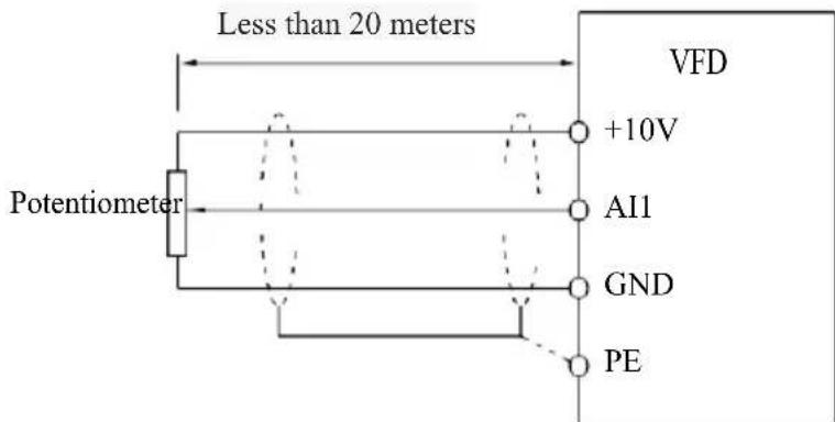
Figure 3-7 Wiring diagram of analog input terminal
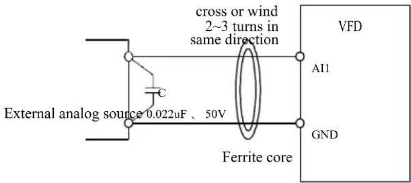
Figure 3-8 Treatment wiring diagram of analog input terminal
b) Digital input terminal: wiring method of DI terminal
Shield cable is commonly used and wiring distance is as short as possible, which should not exceed 20m. If using active way to drive, necessary smoothing measures should be adopted for crosstalk of power. It's suggested to use contactor control way.
Leak-type wiring way-
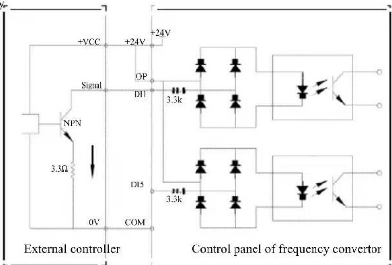
Figure 3-9 Leak-type wiring way
This is the commonest wiring way. If using external power, pull out jumper J9 between +24V and OP, connect positive pole of external power to OP and negative pole of external power to CME.
Source-type wiring way
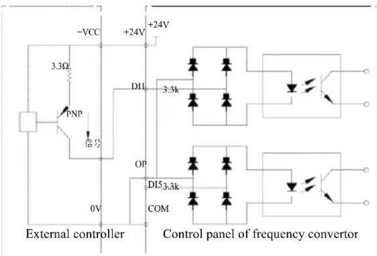
Figure 3-10 Source-type wiring way
This kind of wiring way needs to jump OP of jumper J9 to COM, connect +24V to common port of external controller. If using external power, connect negative pole of external power to OP. c ) DO digital output terminal: if digital output terminal needs to drive relay, absorber diode should be installed on two sides of relay coil, otherwise DC 24V power may be damaged.
Caution: install the polarity of absorber diode correctly as shown in Figure 3-11. Otherwise, if any output of digital output terminal, it will damage DC 24V power immediately.
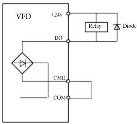
Figure 3-11 Wiring diagram of digital output terminal
Chapter 4 Operation and Display
4.1 Interface introductions of operation and display
The operating panel can modify the function parameters of frequency converter, monitor the working status of the frequency converter, control the running of the frequency converter (start, halt), etc. The exterior and function area are shown as below:

Figure 4-1 Schematic diagram of operation panel
1) Instructions of function indicator light:
RUN: When the light is off, it means the converter is in halt state. When the light is bright, it means the converter is in running state.
LOCAL / REMOT: Keyboard operation, terminal operation and remote operation (communication control) indicating light. When the light is off, it means the keyboard operation control state. If the light is bright, it means terminal operation control state. If the light flickers, it means it is in remote control state.
FWD / REV: Reversing light, when the light is bright it means it is in normal running state.
TUNE / TC: Tune / Torque Control / Fault Indicating Lamp, bright light means it is in torque control mode. Slow flickering light means it is in tune state. Fast flickering light means it is in fault state.
2) Unit indicator light:
Hz: frequency unit
A: current unit
V: voltage unit
RMP (Hz+A) Rotate speed unit % (A+V)
Percentage
3) Digital display:
5-bit LED display displays setting frequency, output frequency, kinds of monitoring data and warning code, etc.
4) Instructions of keyboard button
Table 4-1 Keyboard function
| Key | Name | Function |
| DATA | Programming key | Enter or exit first-level menu |
| ENTER | Enter key | Enter menu step-by-step, set parameters and confirm them |
| [TBTT] | Increasing key | Incremental data or function code |
 | Decreasing key | Decrement data or function code |
 | Shift key | In the stop display interface and running display interface, you can cycle through display parameters; when modifying parameters, you can modify the parameters of the bit |
| RUN | Running key | In keyboard mode, used to run the operation |
| STOP/REST | Stop / Reset | When running, press this button can be used to stop the operation; fault alarm state, it can be used to reset the key features that restrict the function code P7-02 |
| QSM | Menu mode selection key | Function switch based on PP-03 |
| JOG | Jog Key | Function switch based on P7-01, defined as command source or quickly switch direction |
4.2 Viewing and modifying methods of function code
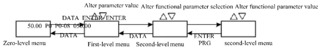
Operation panel, frequency converter adopts three-level menu structure for parameter settings and other operations. Three-level menus are: function parameter group (first level)→function code (second level)→function code setting (second level). Operational flow is shown in Figure 4-2.
flowchart
graph LR
    A["Zero-level menu"] -->|DATA| B["First-level menu"]
    B -->|DATA| C["Second-level menu"]
    C -->|ENTER| D["second-level menu"]
    B -->|DATA ENTER| E["Δ ▽"]
    C -->|Δ ▽| F["Δ ▽"]
    style A fill:#f9f,stroke:#333
    style B fill:#ccf,stroke:#333
    style C fill:#cfc,stroke:#333
    style D fill:#fcc,stroke:#333
Figure 4-2 Flow chart of three-level menus
Instructions: when operating second-level menu, press the DATA key or ENTER key to return to the second-level menu. The difference is: press ENTER to save the setup parameter and return to the second-level menu, and then automatically shift to the next function code; press the SET key will directly return to the second-level menu without saving the parameters, and return to the current function code.
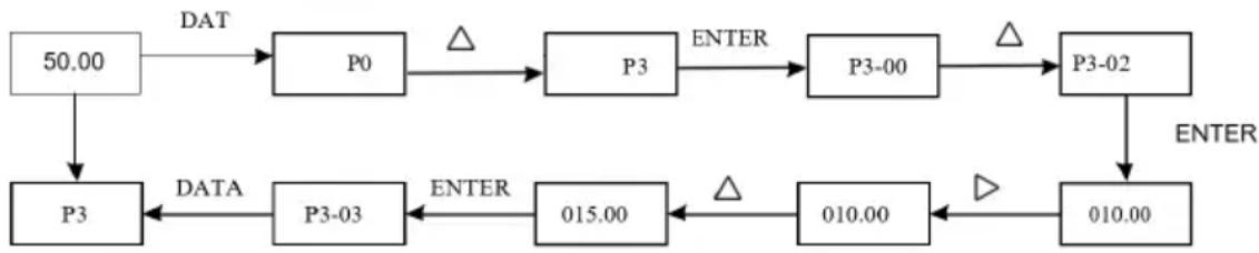
Example: the function code P3-02 is set to change from 10.00Hz
15.00Hz. (Bold text indicates the flashing bit)
flowchart
graph TD
    A["50.00"] -->|DAT| B["P0"]
    B -->|Δ| C["P3"]
    C -->|ENTER| D["P3-00"]
    D -->|Δ| E["P3-02"]
    E -->|ENTER| F["010.00"]
    F -->|Δ| G["015.00"]
    G -->|DATA| H["P3"]
    H -->|DATA| I["P3-03"]
    I -->|ENTER| J["015.00"]
Under status of second-level menu, if there is no flashing bit for parameters, the function code can't be modified, and the possible reasons are below:
1) The function code is parameter that can't be modified, such as actual detection parameter and
operation record parameter, etc.
2) The function code can't be modified under running status, and it can only be modified afterhalting.
4.3 Parameter display mode
Parameter display mode is mainly set for users to view functional parameters with different spread patterns based on actual demand, and there are three parameter display modes.
| Name Description | |
| Functional parameter mode | Display functional parameters of frequency convertor in order, including P0~PF, A0~AF, U0~UF functional parameter |
| User-defined parameter mode | User-defined functional parameters (define 32 parameters at most), users can confirm functional parameters to be displayed through PE group |
| User-modified parameter mode | Functional parameters being not consistent with factor default |
Related functional parameters are PP-02 and PP-03 as below:
| PP-02 | Functional parameter mode display property | Factory default | 11 | |
| Setting range | Unit | U group display selection | ||
| 0 | Not display | |||
| 1 Display | ||||
| Decade | A group display selection | |||
| 0 | Not display | |||
| 1 Display | ||||
| PP-03 | Defined parameter mode display selection | Factory default | 00 | |
| Setting range | Unit | User-defined parameter display selection | ||
| 0 Not display | ||||
| 1 | Display | |||
| Decade | User-modified parameter display selection | |||
| 0 Not display | ||||
| 1 | Display | |||
If defined parameter mode display selection (PP-03) exists to be one display, different parameter display modes can be switched through QSM key.
Display code of each parameter display mode is as below:
| Parameter display mode Display | |
| Functional parameter mode | - bASE |
| User-defined parameter mode | -115Fr |
| User-modified parameter mode | -- [ -- |
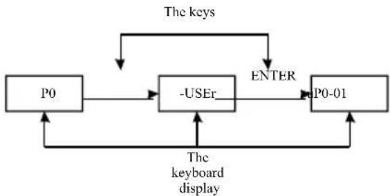
Switching mode is as follows:
The current way for function parameters, switch to a custom parameters
flowchart
graph TD
    A["P0"] --> B["-USEr"]
    B --> C["P0-01"]
    C -->|ENTER| B
    B -->|The keyboard display| A
    style A fill:#f9f,stroke:#333
    style B fill:#ccf,stroke:#333
    style C fill:#cfc,stroke:#333
4.4 user customization parameters
The establishment of the user's customized menu is mainly to facilitate users to view and modify the commonly used functional parameters. The parameters of customized menu display in the form of "uP3-02", it is said that the function of parameter P3-02 in the custom menu to modify the parameters and modify the parameters of the effect of the corresponding programming in general condition is the same.
User customized menu function parameters from the PE group, by the PE group to select the functional parameters, set to P0-00 is not selected
Choose, can be set to 30; if the menu when the display "NULL", which means that the user to customize the menu.
When the initial user custom menu has been deposited in the commonly used 16 parameters to facilitate the user to use:
| P0-01: control mode | P0-02: command source selection |
| P0-03: dominant frequency source selection | P0-07: frequency source selection |
| P0-08: preset frequency | P0-17: acceleration time |
| P0-18: deceleration time | P3-00:V/F curve setting |
| P3-01: torque boost | P4-00:DI1 terminal function selection |
| P4-01:DI2 terminal function selection | P4-02:DI3 terminal function selection |
| P5-04:DO1 output selection | P5-07:AO1 output selection |
| P6-00: start mode | P6-10: stop mode |
Users can according to their own specific needs to be customized for the user to edit.
4.5 Method for viewing state parameter
Under the outage or running state, Through the shift key“▷”Can display a variety of state parameter, respectively. By the function code P7-03 (running parameters 1), P7-04 (operation parameters (2), P7-05 (parameters) downtime by binary bit choose whether to display the parameters.
In stop state, with a total of 16 parameters can choose whether show stop condition respectively: set frequency, bus electric pressure, DI input state, the DO output state, voltage analog input AI1, AI2 analog input voltage, the analog input voltage AI3, actual count value, the actual length value, PLC operation step, load speed display, PID setting, PULSE input PULSE frequency and three reserve parameters, switch input sequences show that the selected parameters.
In running state, the running state of the five parameters: Operating frequency, set frequency, busbar voltage, output voltage, output current for the default display, other display parameters: Output power, output torque, DI input state, the DO output state, voltage analog input AI1, AI2 analog input voltage, the analog input voltage AI3, actual count value, the actual length value, linear velocity, PID, PID feedback is displayed by the function code P7-03, P7-04 bitwise (converted to binary) selection, switch input sequences show that the selected parameters.
Inverter power again to electricity, the display parameter is the default for inverter power lost before the choice of parameters.
4.6 Password settings
Frequency converter provides the user password protection function, when the PP - 00 is set to zero, is the user's password, exit function code editor state password protection is effective, once again, press the DATA, will show "-- -- -- -- --", input user password must be correct, can enter ordinary menu, otherwise unable to enter.
If you want to cancel the password protection function, it is only through the password to enter, and PP - 00 to 0.
4.7 Automatic tuning of motor parameters
Choose the vector control operation mode, in front of the frequency converter operation, must be accurate input motor nameplate parameters, this frequency converter on the basis of standard motor nameplate parameters matching parameters; Vector control method of motor parameters dependence is very strong, to get good control performance, must be charged with the accurate parameters of the machine.
Motor parameters automatic tuning steps are as follows:
Will first command source (P0-02) choice for operation panel command channel. Then please click the parameters of the motor under the actual parameter input (according to the current motor choice):
| Motor selection | parameter |
| Motor 1 | P1-00: motor type selection P1-01: motor rated power P1-02: motor rated voltage P1-03: the motor rated current P1-04: motor rated frequency P1-05: motor rated speed |
| Motor 2 | A2-00: motor types to choose A2-01: motor rated power A2-02: motor rated voltage A2-03: the motor rated current A2-04: A2-05: motor rated frequency motor rated speed |
If the motor can be completely off load, and then the P1-37 (motor 2 A2 \ to 37) please select 2 (asynchronous machine complete tuning), and then press the RUN key on the keyboard panel, the inverter will automatically calculate the motor of the following parameters:
| Motor selection | parameter |
| Motor 1 | P1-06: synchronous machine stator resistance P1-07:synchronous machine D axis inductance P1-08: synchro Q axis inductance P1-09: mutual inductance of the asynchronous motorP1-10: asynchronous motor no-load current |
| Motor 2 | A2-06: synchronous machine stator resistance A2-07:synchronous machine D axis inductanceA2-08: synchro Q axis inductance A1-09: mutual inductance of the asynchronous motorA1-10: asynchronous motor no-load current |
The motor parameters are automatically tuned.
If the motor and the load can not be completely torn off, then P1-37 (motor 2 A2-37) select 1 (asynchronous machine, static tuning) and then press the RUN key on the keyboard panel
Chapter 5 Functional parameter table
PP-00 is set to be non-zero value, namely setting the parameter protection password. Under mode of functional parameter amd user-modified parameter, the parameter menu can only be accessed after entering correct password. To cancel the password, PP-00 needs to be set as 0.
Parameter menu under mode of user-modified parameter is not protected with password. P group and A group are basic function parameters, U group is monitoring parameter. The symbols in functional table are as follows:
“☆”: It indicates the set value of the parameter can be changed under halt and running status of frequency convertor;
“★”: It indicates the set value of the parameter can not be changed under running status of frequency convertor;
“●”: It indicates the value of this parameter is the actually measured value and can not be changed;
“*”: It indicates that the parameter is “factory default” and can only be set by the manufacturer, and users are prohibited to operate;
Table of basic functional parameters
| Code | Name | Setting range | Default | Change |
| P0 basic function group | ||||
| P0-00 | G / P Display type | 1: G Type (Constant torque load model)2: P Type (Fan and pump load model) | Depend on machine type | ● |
| P0-01 | 1^st motor control mode | 0: No speed Sensor vector control (SVC)1: Speed sensor vector control (FVC)2: V / F control | 0 | ★ |
| P0-02 | Command source selection | 0: Operation panel CMD channel (LED off)1: Terminal CMD channel (LED lights)2: Cmd channel (LED flashes)0: Digital setting (Preset frequency P0-08, UP / DOWN can be modified, memory after power failure)1: Digital setting (Preset frequency P0-08, UP / DOWN can be modified, no memory after power failure) | 0 | ☆ |
| P0-03 | Main frequency source X selection | 2: AI13: AI24: AI35: PULSE setting (DI5)6: Multi-stage command7: Simple PLC8: PID9: Communication given | 0 | ★ |
| P0-04 | Auxiliary frequency source Y selection | Same as P0-03 (Main frequency source X selection) | 0 | ★ |
| P0-05 | Auxiliary superimposed frequency source Y range selection | 0 : Relative to the maximum frequency1 : Relative to frequency source X | 0 | ☆ |
| P0-06 | Auxiliary superimposed frequency source Y range selection | 0%~150% | 100% | ☆ |
| Code | Name | Setting range | Default | Change |
| P0-07 | Frequency source superimposed selection | Bits: Frequency source selection0: Main frequency source X1: Main and auxiliary operation result (Operation relation depends on decimal)2: Switch of main frequency source X and auxiliary frequency source Y3: Main frequency source X, main and auxiliary operation result switch4: Auxiliary frequency source Y, main and auxiliary operation result switchDecimal: operation relation of main and auxiliary frequency source0: Main + auxiliary1: Main-auxiliary2: Max. of the two3: Min. of the two | 00 | ☆ |
| P0-08 | Preset frequency | 0.00Hz~maximum frequency (P0-10) | 50.00Hz | ☆ |
| P0-09 | Running direction | 0 : Same direction1 : Opposite direction | 0 | ☆ |
| P0-10 | Maximum frequency | 50.00Hz~600.00Hz | 50.00Hz | ★ |
| P0-11 | Upper frequency source | 0: P0-12 setting1: AI1; 2: AI2; 3: AI3; 4: PULSE setting5: Communication given | 0 | ★ |
| P0-12 | Upper frequency | Upper frequency P0-14~maximum frequency P0-10 | 50.00Hz | ☆ |
| P0-13 | Upper frequency offset | 0.00Hz~maximum frequency P0-10 | 0.00Hz | ☆ |
| P0-14 | Lower frequency | 0.00Hz~upper frequency P0-12 | 0.00Hz | ☆ |
| P0-15 | Carrier frequency | 0.5kHz~16.0kHz | machine type | ☆ |
| P0-16 | carrier frequency adjusts with temperature | 0: no1: yes | 1 | ☆ |
| P0-17 | Acceleration time 1 | 0.00s~65000s | machine type | ☆ |
| P0-18 | Deceleration time 1 | 0.00s~65000s | machine type | ☆ |
| P0-19 | Acceleration/Deceleration time unit | 0: 1s1: 0.1s2: 0.01s | 1 | ★ |
| P0-21 | Auxiliary superimposed frequency source bias frequency | 0.00Hz~maximum frequency P0-10 | 0.00Hz | ☆ |
| P0-22 | Resolution frequency command | 1: 0.1Hz2: 0.01Hz | 2 | ★ |
| P0-23 | Digital setting frequency stop memory selection | 0: no memory 1: memory | 0 | ☆ |
| P0-24 | Motor selection | 0: Motor 1, 1: Motor 2 | 0 | ★ |
| P0-25 | Acceleration/Deceleration time reference frequencies | 0: maximum frequency (P0-10)1: Set frequency2: 100Hz | 0 | ★ |
| P0-26 | Frequency command in operation UP/DOWN standard | 0: Operating frequency, 1: Set frequency | 0 | ★ |
| Code | Name | Setting range | Default | Change |
| P0-27 | Frequency source and command source in bundle | Bits: operation panel command binds frequency source0: Unbound1: Digital set frequency2: AI13: AI24: AI35: PULSE setting (DI5)6: Multispeed7: Simple PLC8: PID9: Communication givenTen bits: terminal command binds frequency sourceHundred bits: communication command binds frequency sourceThousand bits: automatic operation binds frequency source | 0000 | ☆ |
| P0-28 | Communication expansion card type | 0: Modbus communication card1: Spare2: Spare3: CANlink communication card | 0 | ☆ |
| Parameter of 1stmotor in P1 group | ||||
| P1-00 | Type selection of motor | 0: common asynchronous motor1: variable frequency asynchronous motor | 0 | ★ |
| P1-01 | Rated power of motor | 0.1kW~1000.0kW | machine type | ★ |
| P1-02 | Rated voltage of motor | 1V~400V | machine type | ★ |
| P1-03 | Rated current of motor | 0.01A~655.35A (convertor power <=55kW)0.1A~6553.5A (convertor power >55kW) | machine type | ★ |
| P1-04 | Rated frequency of motor | 0.01Hz~max. frequency | machine type | ★ |
| P1-05 | Rated speed of motor | 1rpm~65535rpm | machine type | ★ |
| P1-06 | Stator resistance of asynchronous motor | 0.001 Ω~65.535Ω (convertor power <=55kW)0.0001Ω~6.5535Ω (convertor power >55kW) | Tunning | ★ |
| P1-07 | Rotor resistance of asynchronous motor | 0.001 Ω~65.535Ω (convertor power <=55kW)0.0001Ω~6.5535Ω (convertor power >55kW) | Tunning | ★ |
| P1-08 | Leakage inductive reactance of asynchronous motor | 0.01mH~655.35mH (convertor power <=55kW)0.001mH~65.535mH (convertor power >55kW) | Tunning parameter | ★ |
| P1-09 | Mutual inductive reactance of asynchronous motor | 0.1mH~6553.5mH (convertor power <=55kW)0.01mH~655.35mH (convertor power >55kW) | Tunning parameter | ★ |
| P1-10 | No-load current of asynchronous motor | 0.01A~P1-03 (convertor power <=55kW)0.1A~P1-03 (convertor power >55kW) | Tunning parameter | ★ |
| Code | Name | Setting range | Default | Change |
Specification of high-performance vector convertor
Functional parameter table
| P1-27 | Encoder line number | 1~65535 | 1024 | ★ |
| P1-28 | Encoder type | 0: ABZ incremental encoder1: Spare2: Rotary transformer | 0 | ★ |
| P1-30 | ABZ incremental encoder AB phase sequence | 0: Forward1: Reverse | 0 | ★ |
| P1-34 | Pole-pairs number of rotary transformer | 1~65535 | 1 | ★ |
| P1-36 | Speed feedback PG disconnection detection time | 0.0: no action0.1s~10.0s | 0.0 | ★ |
| F1-37 | Tuning selection | 0: No operation1: Static tuning of asynchronous motor2: Complete tuning of asynchronous motor | 0 | ★ |
| Vector control parameters of 1^st motor in P2 group | ||||
| P2-00 | Speed loop proportional gain 1 | 1~100 | 30 | ☆ |
| P2-01 | Speed loop integral time 1 | 0.01s~10.00s | 0.50s | ☆ |
| P2-02 | Switching frequency 1 | 0.00~P2-05 | 5.00Hz | ☆ |
| P2-03 | Speed loop proportional gain 2 | 1~100 | 20 | ☆ |
| P2-04 | Speed loop integral time 2 | 0.01s~10.00s | 1.00s | ☆ |
| P2-05 | Switching frequency 2 | P2-02~max. frequency | 10.00Hz | ☆ |
| P2-06 | Vector control slip gain | 50%~200% | 100% | ☆ |
| P2-07 | Speed loop filter time constant | 0.000s~0.100s | 0.000s | ☆ |
| P2-08 | Vector control over excitation gain | 0~200 | 64 | ☆ |
| P2-09 | Upper limit source under speed control mode | 0: Setting of function code P2-101: AI12: AI23: AI34: PULSE setting5: Communication given6: MIN (AI1, AI2)7: MAX (AI1, AI2)Full scale of 1-7 option correspond to P2-10 | 0 | ☆ |
| P2-10 | Digital setting of torque under speed control mode | 0.0%~200.0% | 150.0% | ☆ |
| P2-13 | Excitation proportional gain | 0~60000 | 2000 | ☆ |
| P2-14 | Excitation integral gain | 0~60000 | 1300 | ☆ |
| P2-15 | Torque control proportional gain | 0~60000 | 2000 | ☆ |
| Code | Name | Setting range | Default | Change |
Specification of high-performance vector convertor
Functional parameter table
| P2-16 | Torque control integral gain | 0~60000 | 1300 | ☆ |
| V/F control parameters in P3 group | ||||
| P3-00 | VF curve setting | 0: Straight line V/F1: Multipoint V/F2: Square V/F3: 1.2 power V/F4: 1.4 power V/F6: 1.6 power V/F8: 1.8 power V/F9: Reserve10: VF complete separation mode11: VF semi-separation mode | 0 | ★ |
| P3-01 | Torque boost | 0.0% : (Automatic torque boost)0.1%~30.0% | machine type | ☆ |
| P3-02 | Cut-off frequency of torque boost | 0.00Hz~max. frequency | 50.00Hz | ★ |
| P3-03 | Multi-point VF frequency point 1 | 0.00Hz~P3-05 | 0.00Hz | ★ |
| P3-04 | Multi-point VF voltage point 1 | 0.0%~100.0% | 0.0% | ★ |
| P3-05 | Multi-point VF frequency point 2 | P3-03~P3-07 | 0.00Hz | ★ |
| P3-06 | Multi-point VF voltage point 2 | 0.0%~100.0% | 0.0% | ★ |
| P3-07 | Multi-point VF frequency point 3 | P3-05~rated frequency of motor (P1-04) | 0.00Hz | ★ |
| P3-08 | Multi-point VF voltage point 3 | 0.0%~100.0% | 0.0% | ★ |
| P3-09 | VF slip compensation gain | 0.0%~200.0% | 0.0% | ☆ |
| P3-10 | VF over excitation gain | 0~200 | 64 | ☆ |
| P3-11 | VF oscillation suppression gain | 0~100 | machine type | ☆ |
| P3-13 | VF isolated voltage source | 0: Digital setting (P3-14)1: AI12: AI23: AI34: PULSE setting (DI5)5: Multi-stage command6: Simple PLC7: PID8: Communication givenNote: 100.0% correspond to the motor rated voltage | 0 | ☆ |
| P3-14 | VF isolated digital voltage setting | 0V~rated voltage of motor | 0V | ☆ |
| P3-15 | VF isolated voltage rise time | 0.0s~1000.0sNote: time for 0V changes to rated voltage of motor | 0.0s | ☆ |
| Code | Name | Setting range | Default | Change |
| Input terminal of P4 group | ||||
| P4-00 | Function selection of D11 terminal | 0: No function1: Forward running (FWD)2: Reverse running (REV)3: Three-wire run control4: Forward jog (FJOG)5: Reverse jog (RJOG)6: Terminals UP7: Terminals DOWN8: Free halt9: Reset bug (RESET) | 1 | ★ |
| P4-01 | Function selection of D12 terminal | 4 | ★ | |
| P4-02 | Function selection of D13 terminal | 10: Pause operation11: External fault normally open input12: Multi-stage command terminal 113: Multi-stage command terminal 214: Multi-stage command terminal 315: Multi-stage command terminal 416: Acceleration/Deceleration time selection terminal 117: Acceleration/Deceleration time selection terminal 218: Frequency source switching19: UP / DOWN setting cleared (terminal and keyboard)20: Running command switching terminal21: Prohibit acceleration/deceleration22: PID pause23: PLC state reset | 9 | ★ |
| P4-03 | Function selection of D14 terminal | 12 | ★ | |
| P4-04 | Function selection of D15 terminal | 13 | ★ | |
| P4-05 | Function selection of D16 terminal | 24: Swing frequency pause25: Counter input 26: Counter reset27: Length count input 28: Length reset29: Torque control disabled30: PULSE frequency input (valid for D15)31: Reserve32: Prompt DC braking33: External fault normally closed input34: Frequency modification enabled35: PID action direction negated36: Exterior halt terminal 137: Control command switching terminal 238: PID integral pause39: Switch of frequency source X and prese frequency40: Switch of frequency source Y and prese frequency41: Motor selection terminal 142: Motor selection terminal 243: PID parameter switching44: User-defined fault 145: User-defined fault 246: Speed control / torque control switch47: Emergency halt48: Exterior halt terminal 249: Decelerated DC braking50: The running time is cleared51-59: Reserve | 0 | ★ |
| P4-06 | Function selection of D17 terminal | 0 | ★ | |
| P4-07 | Function selection of D18 terminal | 0 | ★ | |
| P4-08 | Function selection of D19 terminal | 0 | ★ | |
| P4-09 | Function selection of D110 terminal | |||
| P4-10 | DI filtering time | 0.000s~1.000s | 0.010s | ☆ |
| P4-11 | Terminal command mode | 0: two-wire 1 1: two-wire 22: three-wire 1 3: three-wire 2 | 0 | ★ |
| P4-12 | Terminal UP/DOWN change rate | 0.001Hz/s~65.535Hz/s | 1.00Hz/s | ☆ |
| P4-13 | AI curve 1 Min. input | 0.00V~P4-15 | 0.00V | ☆ |
| P4-14 | Setting of AI curve 1 Min. input | -100.0%~+100.0% | 0.0% | ☆ |
| P4-15 | AI curve 1 Max. input | P4-13~+10.00V | 10.00V | ☆ |
| P4-16 | Setting of AI curve 1 Max. input | -100.0%~+100.0% | 100.0% | ☆ |
| P4-17 | AI1 filtering time | 0.00s~10.00s | 0.10s | ☆ |
| P4-18 | AI curve 2 Min. input | 0.00V~P4-20 | 0.00V | ☆ |
| P4-19 | Setting of AI curve 2 Min. input | -100.0%~+100.0% | 0.0% | ☆ |
| P4-20 | AI curve 2 Max. input | P4-18~+10.00V | 10.00V | ☆ |
| P4-21 | Setting of AI curve 2 Max. input | -100.0%~+100.0% | 100.0% | ☆ |
| P4-22 | AI2 filtering time | 0.00s~10.00s | 0.10s | ☆ |
| P4-23 | AI curve 3 Min. input | -10.00V~P4-25 | -10.00V | ☆ |
| P4-24 Setting of AI curve 3 Min. input | -100.0%~+100.0% | -100.0% | ☆ | |
| P4-25 | AI curve 3 Max. input | P4-23~+10.00V | 10.00V | ☆ |
| P4-26 | Setting of AI curve 3 Max. input | -100.0%~+100.0% | 100.0% | ☆ |
| P4-27 | AI3 filtering time | 0.00s~10.00s | 0.10s | ☆ |
| P4-28 | PULSE Min. input | 0.00kHz~P4-30 | 0.00kHz | ☆ |
| P4-29 | Setting of PULSE Min. input | -100.0%~100.0% | 0.0% | ☆ |
| P4-30 | PULSE Max. input | P4-28~100.00kHz | 50.00kHz | ☆ |
| P4-31 | Setting of PULSE Max. input | -100.0%~100.0% | 100.0% | ☆ |
| P4-32 | PULSE filtering time | 0.00s~10.00s | 0.10s | ☆ |
| P4-33 | AI curve selection | Bit: AI1 curve selection1: Curve 1 (2 point, see P4-13~P4-16)2: Curve 2 (2 point, see P4-18~P4-21)3: Curve 3 (2 point, see P4-23~P4-26)4: Curve 4 (4 point, see A6-00~A6-07)5: Curve 5 (4 point, see A6-08~A6-15)Ten bit: AI2 curve selection, same as above Hundred bit: AI2 curve selection, same | 321 | ☆ |
| P4-34 | AI is below Min. input setting selection | Bit: AI1 is below the minimum input setting0: correspond to min. input setting 1: 0.0%Ten bit: AI2 is below min. input setting AI3 is below min. input setting | 000 | ☆ |
| P4-35 | DI1 delay time | 0.0s~3600.0s | 0.0s | ★ |
| P4-36 | DI2 delay time | 0.0s~3600.0s | 0.0s | ★ |
| P4-37 | DI3 delay time | 0.0s~3600.0s | 0.0s | ★ |
| P4-38 | Effective mode selection 1 of DI terminal | 0: valid high-level1: valid low-levelBit: DI1 Ten bit: DI2 Hundred bit: DI3 Thousand bit: DI4 Ten thousand bit: DI5 | 00000 | ★ |
| P4-39 | Effective mode selection 2 of DI terminal | 0: valid high-level1: valid low-levelBit:DI6 Ten bit: DI7 Hundred bit:DI8 Thousand bit: DI9 Ten thousand bit: DI10 | 00000 | ★ |
| Output terminal of P5 group | ||||
| P5-00 | Output mode selection of FM terminal | 0: Pulse output (FMP)1: Switching output (FMR) | 0 | ☆ |
| P5-01 | FMR output function selection | 0: No output | 0 | ☆ |
| P5-02 | Relay function selection of control panel (T/A-T/B-T/C) | 1: Operation of frequency convertor2: Fault output (downtime)3: Frequency level detection output FDT14: Frequency arrival5: Zero speed operation (no output halt)6: Pre-alarm of motor overload | 2 | ☆ |
| P5-03 | Relay function selection of expansion card (P/A-P/B-P/C) | 0 | ☆ | |
| P5-04 | DO1 output function selection | 1 | ☆ | |
| P5-05 | Output selection of expansion card DO2 | 7: Pre-alarm of convertor overload8: Count value reaches the set9: Reaching the set count10: Length arrival11: PLC cycle is complete12: Set the accumulated run time13: Frequency limit14: Torque limit15: Ready to run16: AI1>AI217: Upper limit frequency arrival18: Lower limit frequency reaches (running about)19: Brown-state output20: Communication Preferences21: Positioning complete (reserve)22: Location close (reserve)23: Zero-speed operation 2 (shutdown also output)24: Set the accumulated power-on time25: Frequency level detection output FDT226: 1 to the output frequency27: 2 to the output frequency28: 1 to the output current29: 2 to the output current30: The timing to the output31: AI1 input overrun32: Carrying out33: Reverse operation34: Zero current state35: Module temperature reached36: Output current limit value37: The lower limit frequency arrival (stop output)38: Alarm output (continue)39: Pre-alarm of motor overtemperature40: The running time arrival | 4 | ☆ |
| P5-06 | FMP output function selection | 0: Operation frequency1: Setting frequency2: Output current3: Output torque4: Output power5: Output voltage6: PULSE input (100.% corresponds to 100.0kHz)7: AI18: AI29: AI3 (expansion card)10: Length11: Value12: Communication setting13: Motor speed14: Output current (100.0% is 1000.0A)15: Output voltage (100.0% is 1000.0V)16: Reserve | 0 | ☆ |
| P5-07 | AO1 output function selection | 0 | ☆ | |
| P5-08 | Output function selection of expansion card AO2 | 1 | ☆ | |
| P5-09 | FMP maximum output frequency | 0.01kHz~100.00kHz | 50.00kHz | ☆ |
| P5-10 | AO1 zero offset coefficient | -100.0%~+100.0% | 0.0% | ☆ |
| P5-11 | AO1 gain | -10.00~+10.00 | 1.00 | ☆ |
| P5-12 | Zero offset coefficient of expansion card AO2 | -100.0%~+100.0% | 0.0% | ☆ |
| P5-13 | AO2 gain of expansion card AO2 | -10.00~+10.00 | 1.00 | ☆ |
| P5-17 | FMR output delay time | 0.0s~3600.0s | 0.0s | ☆ |
| P5-18 | RELAY1 output delay time | 0.0s~3600.0s | 0.0s | ☆ |
| P5-19 | RELAY2 output delay time | 0.0s~3600.0s | 0.0s | ☆ |
| P5-20 | DO1 output delay time | 0.0s~3600.0s | 0.0s | ☆ |
| P5-21 | DO2 output delay time | 0.0s~3600.0s | 0.0s | ☆ |
| P5-22 | Valid state selection of DO output terminal | 0: positive logic1: negative logicBit: FMR Ten bit: RELAY1Hundred bit: RELAY2 Thousand bit: DO1Ten Thousand bit: DO2 | 00000 | ☆ |
| Start/Halt control of P6 group | ||||
| P6-00 | Start mode | 0: Direct start1: Speed tracking restart2: Start pre-excitation (AC asynchronous motor) | 0 | ☆ |
| P6-01 | Speed tracking mode | 0: Start from stop frequency1: Start from zero speed2: Start from maximum frequency | 0 | ★ |
| P6-02 | Speed tracking speed | 1~100 | 20 | ☆ |
| P6-03 | Start frequency | 0.00Hz~10.00Hz | 0.00Hz | ☆ |
| P6-04 | Start frequency retention time | 0.0s~100.0s | 0.0s | ★ |
| P6-05 | Start DC braking current / Pre-excitation current | 0%~100% | 0% | ★ |
| P6-06 | Start DC braking time/Pre-excitation time | 0.0s~100.0s | 0.0s | ★ |
| P6-07 | Acceleration and deceleration mode | 0: Linear acceleration and deceleration1: S curve acceleration and deceleration A2: S curve acceleration and deceleration B | 0 | ★ |
| P6-08 | S curve start section time ratio | 0.0%~ (100.0%-P6-09) | 30.0% | ★ |
| P6-09 | S curve ending section time ratio | 0.0%~ (100.0%-P6-08) | 30.0% | ★ |
| P6-10 | Halt mode | 0: Deceleration to halt, 1: Free halt | 0 | ☆ |
| P6-11 | Initial frequency of halt DC braking | 0.00Hz~max. frequency | 0.00Hz | ☆ |
| P6-12 | Waiting time of halt DC braking | 0.0s~100.0s | 0.0s | ☆ |
| P6-13 | Current of halt DC braking | 0%~100% | 0% | ☆ |
| P6-14 | Time of halt DC braking | 0.0s~100.0s | 0.0s | ☆ |
| P6-15 | Brake usage | 0%~100% | 100% | ☆ |
| Keyboard and display of P7 group | ||||
| P7-01 | JOG key function selection | 0: Invalid JOG1: Switch of operation panel CMDchannel and remote CMD channel (terminal CMD channel or CMD channel)2: Reversing switch3: Forward jog | 0 | ★ |
| P7-02 | STOP/RESET key function | 0: Only in keyboard mode, halt function of STOP / RES key is valid1: under any operation mode, halt function of STOP/RES is valid | 1 | ☆ |
| P7-03 | LED running display parameter 1 | 0000~FFFFBit00: running frequency 1 (Hz)Bit01: setting frequency (Hz)Bit02: busbar voltage (V)Bit03: output voltage (V)Bit04: output current (A)Bit05: output power (kW)Bit06: output torque (%)Bit07: DI input stateBit08: DO output stateBit09: AI1 voltage (V)Bit10: AI2 voltage (V)Bit11: AI3 voltage (V)Bit12: Count valueBit13: Length valueBit14: Display loading speedBit15: PID setting | 1F | ☆ |
| P7-04 | LED running display parameter 2 | 0000~FFFF Bit00: PID FeedbackBit01: PLC stageBit02: Pulse Input pulse frequency (kHz)Bit03: Operating frequency 2 (Hz)Bit04: Remaining operating timeBit05: AI1 Before the correction voltage (V)Bit06: AI2 before the correction voltage (V)Bit07: AI3 before the correction voltage (V)Bit08: Line speedBit09: Current power-on time (Hour)Bit10: Current running time (Min)Bit11: PULSE Input pulse frequency (Hz)Bit12: Communication set valueBit13: Encoder feedback speed (Hz)Bit14: Main frequency X display (Hz)Bit15: Frequency Y display (Hz) | 0 | ☆ |
| P7-05 | LED halt display parameters | 0000~FFFFBit00: Set frequency (Hz)Bit01: Bus voltage (V)Bit02: DI Input StatusBit03: DO OutputstatusBit04: AI1Voltage (V)Bit05: AI2 Voltage (V)Bit06: AI3 Voltage (V)Bit07: The count valueBit08: Length valueBit09: PLC StageBit10: Load SpeedBit11: PID Set upBit12: Pulse Input pulse frequency (kHz) | 33 | ☆ |
| P7-06 | Load speed display coefficient | 0.0001~6.5000 | 1.0000 | ☆ |
| P7-07 | Radiator temperature of inverter | 0.0°C~100.0°C | - | ● |
| P7-08 | Radiator temperature of rectifier | 0.0°C~100.0°C | - | ● |
| P7-09 | Total running time | 0h~65535h | - | ● |
| P7-10 | Product No. | - | - | ● |
| P7-11 | Software version number | - | - | ● |
| P7-12 | Load speed display decimal digits | 0: 0 decimal places1: 1 decimal places2: 2 decimal places3: 3 decimal places | 1 | ☆ |
| P7-13 | Cumulative power-up time | 0h~65535h | - | ● |
| P7-14 | Total power consumption | 0~65535KWh | - | ● |
| Auxiliary function of P8 group | ||||
| P8-00 | Jog frequency | 0.00Hz~max. frequency | 2.00Hz | ☆ |
| P8-01 | Jog acceleration time | 0.0s~6500.0s | 20.0s | ☆ |
| P8-02 | Jog deceleration time | 0.0s~6500.0s | 20.0s | ☆ |
| P8-03 | Acceleration time 2 | 0.0s~6500.0s | machine type | ☆ |
| P8-04 | Deceleration time 2 | 0.0s~6500.0s | machine type | ☆ |
| P8-05 | Acceleration time 3 | 0.0s~6500.0s | machine type | ☆ |
| P8-06 | Deceleration time 3 | 0.0s~6500.0s | machine type | ☆ |
| P8-07 | Acceleration time 4 | 0.0s~6500.0s | machine type | ☆ |
| P8-08 | Deceleration time 4 | 0.0s~6500.0s | machine type | ☆ |
| P8-09 | Hopping frequency 1 | 0.00Hz~max. frequency | 0.00Hz | ☆ |
| P8-10 | Hopping frequency 2 | 0.00Hz~max. frequency | 0.00Hz | ☆ |
| P8-11 | Hopping frequency range | 0.00Hz~max. frequency | 0.01Hz | ☆ |
| P8-12 | Reversible dead time | 0.0s~3000.0s | 0.0s | ☆ |
| P8-13 | Inversion of control enables | 0: allow 1: prohibit | 0 | ☆ |
| P8-14 | Operation mode of set frequency being lower than lower limit frequenc | 0: operate at lower limit frequency1: halt2: zero-speed operation | 0 | ☆ |
| P8-15 | Droop control | 0.00Hz~10.00Hz | 0.00Hz | ☆ |
| P8-16 | Set accumulated power-on time | 0h~65000h | 0h | ☆ |
| P8-17 | Set accumulated run time | 0h~65000h | 0h | ☆ |
| P8-18 | Start protection selection | 0: no protection 1: protection | 0 | ☆ |
| P8-19 | Frequency detection value | 0.00Hz~max. frequency | 50.00Hz | ☆ |
| P8-20 | Frequency detection hysteresis value | 0.0%~100.0% (FDT1 level) | 5.0% | ☆ |
| P8-21 | Frequency arrival detection width | 0.0%~100.0% (max. frequency) | 0.0% | ☆ |
| P8-22 | If jopping frequency is valid in acceleration/deceleration | 0: invalid 1: valid | 0 | ☆ |
| P8-25 | Switch frequency between acceleration time 1 and 2 | 0.00Hz~max. frequency | 0.00Hz | ☆ |
| P8-26 | Switch frequency between deceleration time 1 and 2 | 0.00Hz~max. frequency | 0.00Hz | ☆ |
| P8-27 | Terminal jog priority | 0: invalid 1: valid | 0 | ☆ |
| P8-28 | Frequency detection value | 0.00Hz~max. frequency | 50.00Hz | ☆ |
| P8-29 | Frequency detection hysteresis value | 0.0%~100.0% (FDT2 level) | 5.0% | ☆ |
| P8-30 | Any frequency detection value 1 | 0.00Hz~max. frequency | 50.00Hz | ☆ |
| P8-31 | Any frequency detection width 1 | 0.0%~100.0% (max. frequency) | 0.0% | ☆ |
| P8-32 | Any frequency detection value 2 | 0.00Hz~max. frequency | 50.00Hz | ☆ |
| P8-33 | Any frequency detection width 2 | 0.0%~100.0% (max. frequency) | 0.0% | ☆ |
| P8-34 | Zero-current detection level | 0.0%~300.0% 100.0% is rated current | 5.0% | ☆ |
| P8-35 | Zero-current detection delay time | 0.01s~600.00s | 0.10s | ☆ |
| P8-36 | Output current limit value | 0.0 % (no detection)0.1 %~300.0% (rated current of motor) | 200.0% | ☆ |
| P8-37 | Output current limit detects delay time | 0.00s~600.00s | 0.00s | ☆ |
| P8-38 | Any arrival current 1 | 0.0%~300.0%(rated current of motor) | 100.0% | ☆ |
| P8-39 | Width of any arrival current 1 | 0.0%~300.0%(rated current of motor) | 0.0% | ☆ |
| P8-40 | Any arrival current 2 | 0.0%~300.0%(rated current of motor) | 100.0% | ☆ |
| P8-41 | Width of any arrival current 2 | 0.0%~300.0%(rated current of motor) | 0.0% | ☆ |
| P8-42 | Timing function selection | 0: invalid 1: valid | 0 | ☆ |
| P8-43 | Timing operation time selection | 0: P8-44 setting; 1: AI1; 2: AI2; 3: AI3Anolog input range corresponds to P8-44 | 0 | ☆ |
| P8-44 | Timing operation time | 0.0Min~6500.0Min | 0.0Min | ☆ |
| P8-45 | Lower limit of AI1 input voltage protection value | 0.00V~P8-46 | 3.10V | ☆ |
| P8-46 | Upper limit of AI1 input voltage protection value | P8-45~10.00V | 6.80V | ☆ |
| P8-47 | Module temperature reached | 0°C~100°C | 75°C | ☆ |
| P8-48 | Cooling fan control | 0: The fan operates when running1: The fan has been running | 0 | ☆ |
| P8-49 | Wake frequency | Sleep frequency (P8-51)~maximum frequency (P0-10) | 0.00Hz | ☆ |
| P8-50 | Wake-up delay time | 0.0s~6500.0s | 0.0s | ☆ |
| P8-51 | Sleep frequency | 0.00Hz~wake frequency (P8-49) | 0.00Hz | ☆ |
| P8-52 | Sleep latency | 0.0s~6500.0s | 0.0s | ☆ |
| P8-53 | Arrival time setting of operation | 0.0Min~6500.0Min | 0.0Min | ☆ |
| Fault and protection of P9 group | ||||
| P9-00 | Motor overload protection | 0: allow 1: prohibit | 1 | ☆ |
| P9-01 | Motor overload protection gain | 0.20~10.00 | 1.00 | ☆ |
| P9-02 | Motor overload warning coefficient | 50%~100% | 80% | ☆ |
| P9-03 | Overvoltage stall gain | 0~100 | 0 | ☆ |
| P9-04 | Overvoltage stall protection voltage | 120%~150% | 130% | ☆ |
| P9-05 | Over current stall gain | 0~100 | 20 | ☆ |
| P9-06 | Over current stall protection current | 100%~200% | 150% | ☆ |
| P9-07 | To-ground short circuit protection | 0: invalid 1: valid | 1 | ☆ |
| P9-09 | Auto reset times of fault | 0~20 | 0 | ☆ |
| P9-10 | DO action during auto reset of fault | 0: no action1: action | 0 | ☆ |
| P9-11 | Automatic reset interval of fault | 0.1s~100.0s | 1.0s | ☆ |
| P9-12 | Input phase loss protection | 0: allow 1: prohibit | 1 | ☆ |
| P9-13 | Output phase loss protection | 0: allow 1: prohibit | 1 | ☆ |
| P9-14 | Type of first fault | 0: No fault1: Reserve2: Acceleration overcurrent3: Deceleration overcurrent4: Over current constant5: Overvoltage acceleration6: Deceleration overvoltage7: Constant speed overvoltage8: Buffer overload resistance9: Brown10: Convertor overload11: Motor overload12: Input phase | — | ● |
| P9-15 | Type of second fault | 13: Output phase14: Module overheating15: External fault16: Abnormal communication17: Abnormal contact18: Current detecting abnormal19: Abnormal motor tuning20: Abnormal encoder / PG card21: Abnormal reading/writing parameters22: Hardware exception of convertor23: Hardware exception of convertor24: Reserve25: Reserve | — | ● |
| P9-16 | Type of second (recent) fault | 26: Running time arrival27: User-defined fault 128: User-defined fault 229: Power-on time is reached30: Carrying out31: Runtime PID feedback loss40: Fast current-limit timeout41: When switching the motor running42: Excessive speed deviation43: Motor overspeed45: Motor overtemperature51: The initial position error | — | ● |
| P9-17 | Frequency of second (recent) fault | — | — | ● |
| P9-18 | Current of second (recent) fault | — | — | ● |
| P9-19 | Busbar voltage of second (recent) fault | — | — | ● |
| P9-20 | Input terminal status of second (recent) fault | — | — | ● |
| P9-21 | Output terminal status of second (recent) fault | — | — | ● |
| P9-22 | Convertor status of second (recent) fault | — | — | ● |
| P9-23 | Electrifying time of second (recent) fault | — | — | ● |
Specification of high-performance vector convertor
Functional parameter table
| Code | Name | Setting range | Default | Change |
| P9-24 | Running time of second (recent) fault | — | — | ● |
| P9-27 | Frequency of second fault | — | — | ● |
| P9-28 | Current of second fault | — | — | ● |
| P9-29 | Busbar voltage of second fault | — | — | ● |
| P9-30 | Input terminal status of second fault | — | — | ● |
| P9-31 | Output terminal status of second fault | — | — | ● |
| P9-32 | Convertor status of second fault | — | — | ● |
| P9-33 | Electrifying time of second fault | — | — | ● |
| P9-34 | Running time of second fault | — | — | ● |
| P9-37 | Frequency of first fault | — | — | ● |
| P9-38 | Current of first fault | — | — | ● |
| P9-39 | Busbar voltage of first fault | — | — | ● |
| P9-40 | Input terminal status of first fault | — | — | ● |
| P9-41 | Output terminal status of first fault | — | — | ● |
| P9-42 | Convertor status of first fault | — | — | ● |
| P9-43 | Electrifying time of first fault | — | — | ● |
| P9-44 | Running time of first fault | — | — | ● |
| Bit: Motor overload (11) | ||||
| 0: Free halt | ||||
| 1: Stop according to stop mode | ||||
| 2: Continue to run | ||||
| Ten bit: Input phase (12) | 00000 | ☆ | ||
| Hundred bit: Output phase (13) | ||||
| Thousand bit: External fault (15) | ||||
| Ten thousand bit: Abnormal communication (16) | ||||
| Bit: Abnormal encoder / PG card (20) | ||||
| 0: Free halt | ||||
| Ten bit: Abnormal function code reader (21) | ||||
| P9-48 | Fault protection action selection 2 | 0: Free halt | ||
| 1: Stop according to stop mode | 00000 | ☆ | ||
| Hundred bit: Reserve | ||||
| Thousand bit: Motor overheating (25) | ||||
| Ten thousand bit: Running time arrival (26) | ||||
| P9-49 | Fault protection action selection 3 | Bit: User-defined fault 1 (27)0: Free halt1: Stop according to stop mode2: Continue to runHundred bit: Power-on time is reached (29)Thousand bit: Carrying out (30)0: Free halt1: Deceleration to stop2: Decelerated to 7% of the rated motor frequency continues to run, When you can not afford to load automatically restored to the set frequency operationTen thousand bit: Runtime PID feedback loss (31)0: Free halt1: Stop according to stop mode2: Continue to run | 00000 | ☆ |
| P9-50 | Fault protection action selection 4 | Bit: Excessive speed deviation (42)0: Free halt1: Stop according to stop mode2: Continue to runTen bit: Super speed motor (43)Hundred bit: The initial position error (51) | 00000 | ☆ |
| P9-54 | Continue to run frequency selection when fault happens | 0: In the current operating frequency operation1: Run at set frequency2: Run at upper limit frequency3: Lower limit frequency operation4: Alternate abnormal frequency operation | 0 | ☆ |
| P9-55 | Abnormal alternative frequency | 60.0%~100.0% (100.0% Corresponding to the maximum frequencyP0-10) | 100.0% | ☆ |
| P9-56 | Motor temperature sensor type | 0: no temperature sensor1: PT1002: PT1000 | 0 | ☆ |
| P9-57 | Motor overheating protection threshold | 0°C~200°C | 110°C | ☆ |
| P9-58 | Motor overheating prediction alert threshold | 0°C~200°C | 90°C | ☆ |
| P9-59 | Instantaneous power failure action selection | 0: invalid1: deceleration2: deceleration to halt | 0 | ☆ |
| P9-60 | Retention | P9-62~100.0% | 100.0% | ☆ |
| P9-61 | Instantaneous power voltage recovery judgment time | 0.00s~100.00s | 0.50s | ☆ |
| P9-62 | Instant power cut action judging voltage | 60.0%~100.0% (standard busbar voltage) | 80.0% | ☆ |
| P9-63 | Load missing protectionselection | 0: invalid1: valid | 0 | ☆ |
| P9-64 | Load missing detection level | 0.0~100.0% | 10.0% | ☆ |
| P9-65 | Load missing testing time | 0.0~60.0s | 1.0s | ☆ |
| P9-67 | Over-speed detection value | 0.0%~50.0%(max. frequency) | 20.0% | ☆ |
| P9-68 | Over-speed detection time | 0.0s~60.0s | 5.0s | ☆ |
| P9-69 | Excessive speed deviation detection value | 0.0%~50.0%(max. frequency) | 20.0% | ☆ |
| P9-70 | Excessive speed deviation detection time | 0.0s~60.0s | 0.0s | ☆ |
| PID function of FA group | ||||
| PA-00 | PID given source | 0: PA-01 set up1: AI1; 2: AI2; 3: AI34: Pulse setting (DI5)5: Communication given6: Multi-section instruction given | 0 | ☆ |
| PA-01 | PID values given | 0.0%~100.0% | 50.0% | ☆ |
| PA-02 | PID feedback source | 0: AI1; 1: AI2; 2: AI3; 3: AI1-AI24: PULSE setting (DI5)5: Communication given6: AI1+AI27: MAX (|AI1|, |AI2|)8: MIN (|AI1|, |AI2|) | 0 | ☆ |
| PA-03 | PID action direction | 0: positive action1: negative action | 0 | ☆ |
| PA-04 | PID given feedback range | 0~65535 | 1000 | ☆ |
| PA-05 | Proportional gain Kp1 | 0.0~100.0 | 20.0 | ☆ |
| PA-06 | Integration time Ti1 | 0.01s~10.00s | 2.00s | ☆ |
| PA-07 | Differential time Td1 | 0.000s~10.000s | 0.000s | ☆ |
| PA-08 | PID reverse cut-off frequency | 0.00~max. frequency | 2.00Hz | ☆ |
| PA-09 | PID deviation limit | 0.0%~100.0% | 0.0% | ☆ |
| PA-10 | PID differential limiting | 0.00%~100.00% | 0.10% | ☆ |
| PA-11 | PID given change time | 0.00~650.00s | 0.00s | ☆ |
| PA-12 | PID feedback filter time | 0.00~60.00s | 0.00s | ☆ |
| PA-13 | PID output filter time | 0.00~60.00s | 0.00s | ☆ |
| PA-14 | Retention | - | - | ☆ |
| PA-15 | Proportional gainKp2 | 0.0~100.0 | 20.0 | ☆ |
| PA-16 | Integration time Ti2 | 0.01s~10.00s | 2.00s | ☆ |
| PA-17 | Differential time Td2 | 0.000s~10.000s | 0.000s | ☆ |
| PA-18 | PID parameters switching condition | 0: Not switch1: By DI terminal switch2: Automatic switching based on bias | 0 | ☆ |
| PA-19 | PID parameter switching deviation 1 | 0.0%~PA-20 | 20.0% | ☆ |
| PA-20 | PID parameter switching deviation 2 | PA-19~100.0% | 80.0% | ☆ |
| PA-21 | Initial PID | 0.0%~100.0% | 0.0% | ☆ |
| PA-22 | Hold time of initial PID | 0.00~650.00s | 0.00s | ☆ |
| PA-23 | Forward max. of two output bias | 0.00%~100.00% | 1.00% | ☆ |
| PA-24 | Reverse max. of two output bias | 0.00%~100.00% | 1.00% | ☆ |
| PA-25 | PID integral property | Bit: Integral separation0: Invalid; 1: ValidTen bit: Integral to whether to stop the output limit0: Continued integration1: Stop Points | 00 | ☆ |
| PA-26 | PID feedback loss detection value | 0.0%: do not judge feedback loss0.1%~100.0% | 0.0% | ☆ |
| PA-27 | PID feedback loss detection time | 0.0s~20.0s | 0.0s | ☆ |
| PA-28 | PID stoppage operation | 0: Stop operation; 1: Shutdown operation | 0 | ☆ |
| Swing frequency, length and count of Pb group | ||||
| Pb-00 | Setting way of swing frequency | 0: Relative to central frequency1: relative to the maximum frequency | 0 | ☆ |
| Pb-01 | Swing frequency range | 0.0%~100.0% | 0.0% | ☆ |
| Pb-02 | Kick frequency range | 0.0%~50.0% | 0.0% | ☆ |
| Pb-03 | Kick frequency cyle | 0.1s~3000.0s | 10.0s | ☆ |
| Pb-04 | Triangular wave rising time | 0.1%~100.0% | 50.0% | ☆ |
| Pb-05 | Set length | 0m~65535m | 1000m | ☆ |
| Pb-06 | Actual length | 0m~65535m | 0m | ☆ |
| Pb-07 | Number of pulses per meter | 0.1~6553.5 | 100.0 | ☆ |
| Pb-08 | Set count value | 1~65535 | 1000 | ☆ |
| Pb-09 | Designated count value | 1~65535 | 1000 | ☆ |
| Multi-stage command and simple PLC in PC group | ||||
| PC-00 | Multi-stage command 0 | -100.0%~100.0% | 0.0% | ☆ |
| PC-01 | Multi-stage command 1 | -100.0%~100.0% | 0.0% | ☆ |
| PC-02 | Multi-stage command 2 | -100.0%~100.0% | 0.0% | ☆ |
| PC-03 | Multi-stage command 3 | -100.0%~100.0% | 0.0% | ☆ |
| PC-04 | Multi-stage command 4 | -100.0%~100.0% | 0.0% | ☆ |
| PC-05 | Multi-stage command 5 | -100.0%~100.0% | 0.0% | ☆ |
| PC-06 | Multi-stage command 6 | -100.0%~100.0% | 0.0% | ☆ |
| PC-07 | Multi-stage command 7 | -100.0%~100.0% | 0.0% | ☆ |
| PC-08 | Multi-stage command 8 | -100.0%~100.0% | 0.0% | ☆ |
| PC-09 | Multi-stage command 9 | -100.0%~100.0% | 0.0% | ☆ |
| PC-10 | Multi-stage command 10 | -100.0%~100.0% | 0.0% | ☆ |
| PC-11 | Multi-stage command 11 | -100.0%~100.0% | 0.0% | ☆ |
| PC-12 | Multi-stage command 12 | -100.0%~100.0% | 0.0% | ☆ |
| PC-13 | Multi-stage command 13 | -100.0%~100.0% | 0.0% | ☆ |
| PC-14 | Multi-stage command 14 | -100.0%~100.0% | 0.0% | ☆ |
| PC-15 | Multi-stage command 15 | -100.0%~100.0% | 0.0% | ☆ |
| PC-16 | Simple PLC operation mode | 0: Stop at the end of single running1: End of single running holding final value2: Been circulating | 0 | ☆ |
| PC-17 | Memory selection after power failure of simple PLC | Bit: memory selection after power failure0: no memory after power failure1: memory after power failureTen bit: memory selection after halt0: no memory after halt1: memory after halt | 00 | ☆ |
| PC-18 | Simple PLC running time of seg. 0 | 0.0s (h) ~6553.5s (h) | 0.0s (h) | ☆ |
| PC-19 | Simple PLC acceleration/ deceleration time of segment 0 | 0~3 | 0 | ☆ |
| PC-20 | Simple PLC running time of seg. 1 | 0.0s (h)~6553.5s (h) | 0.0s (h) | ☆ |
| PC-21 | Simple PLC acceleration/ deceleration time of segment 1 | 0~3 | 0 | ☆ |
| PC-22 | Simple PLC running time of seg. 2 | 0.0s (h)~6553.5s (h) | 0.0s (h) | ☆ |
| PC-23 | Simple PLC acceleration/ deceleration time of segment 2 | 0~3 | 0 | ☆ |
| PC-24 | Simple PLC running time of seg. 3 | 0.0s (h)~6553.5s (h) | 0.0s (h) | ☆ |
| PC-25 | Simple PLC acceleration/ deceleration time of segment 3 | 0~3 | 0 | ☆ |
| PC-26 | Simple PLC running time of seg. 4 | 0.0s (h)~6553.5s (h) | 0.0s (h) | ☆ |
| PC-27 | Simple PLC acceleration/ deceleration time of segment 4 | 0~3 | 0 | ☆ |
| PC-28 | Simple PLC running time of seg. 5 | 0.0s (h)~6553.5s (h) | 0.0s (h) | ☆ |
| PC-29 | Simple PLC acceleration/ deceleration time of segment 5 | 0~3 | 0 | ☆ |
| PC-30 | Simple PLC running time of seg. 6 | 0.0s (h)~6553.5s (h) | 0.0s (h) | ☆ |
| PC-31 | Simple PLC acceleration/ deceleration time of segment 6 | 0~3 | 0 | ☆ |
| PC-32 | Simple PLC running time of seg. 7 | 0.0s (h)~6553.5s (h) | 0.0s (h) | ☆ |
| PC-33 | Simple PLC acceleration/ deceleration time of segment 7 | 0~3 | 0 | ☆ |
| PC-34 | Simple PLC running time of seg. 8 | 0.0s (h)~6553.5s (h) | 0.0s (h) | ☆ |
| PC-35 | Simple PLC acceleration/ deceleration time of segment 8 | 0~3 | 0 | ☆ |
Specification of high-performance vector convertor
Functional parameter table
| Code | Name | Setting range | Default | Change |
| PC-36 | Simple PLC running time of seg. 9 | 0.0s (h)~6553.5s (h) | 0.0s (h) | ☆ |
| PC-37 | Simple PLC acceleration/ deceleration time of segment 9 | 0~3 | 0 | ☆ |
| PC-38 | Simple PLC running time of seg. 10 | 0.0s (h)~6553.5s (h) | 0.0s (h) | ☆ |
| PC-39 | Simple PLC acceleration/ deceleration time of segment 10 | 0~3 | 0 | ☆ |
| PC-40 | Simple PLC running time of seg. 11 | 0.0s (h)~6553.5s (h) | 0.0s (h) | ☆ |
| PC-41 | Simple PLC acceleration/ deceleration time of segment 11 | 0~3 | 0 | ☆ |
| PC-42 | Simple PLC running time of seg. 12 | 0.0s (h)~6553.5s (h) | 0.0s (h) | ☆ |
| PC-43 | Simple PLC acceleration/ deceleration time of segment 12 | 0~3 | 0 | ☆ |
| PC-44 | Simple PLC running time of seg. 13 | 0.0s (h)~6553.5s (h) | 0.0s (h) | ☆ |
| PC-45 | Simple PLC acceleration/ deceleration time of segment 13 | 0~3 | 0 | ☆ |
| PC-46 | Simple PLC running time of seg. 14 | 0.0s (h)~6553.5s (h) | 0.0s (h) | ☆ |
| PC-47 | Simple PLC acceleration/ deceleration time of segment 14 | 0~3 | 0 | ☆ |
| PC-48 | Simple PLC running time of seg. 15 | 0.0s (h)~6553.5s (h) | 0.0s (h) | ☆ |
| PC-49 | Simple PLC acceleration/ deceleration time of segment 15 | 0~3 | 0 | ☆ |
| PC-50 | Simple PLC running time unit | 0: s (second)1: h (hour) | 0 | ☆ |
| 0: PC-00 function code given1: AI12: AI2 | ||||
| PC-51 | Given way of multi-stage command 0 | 3: AI34: PULSE5: PID6: Preset frequency (P0-08) given, UP / DOWNCan be modified | 0 | ☆ |
Communication parameter of Pd group
| Code | Name | Setting range | Default | Change |
| Pd-00 | Baud rate | Bit: MODBUS0: 300BPS1: 600BPS2: 1200BPS3: 2400BPS4: 4800BPS5: 9600BPS6: 19200BPS7: 38400BPS8: 57600BPS9: 115200BPSTen bit: reserveHundred bit: reserveThousand bit: CANlink Baud rate0: 201: 502: 1003: 1254: 2505: 5006: 1M | 6005 | ☆ |
| Pd-01 | Data format | 0: No inspection (8-N-2)1: Enven parity check (8-E-1)2: Even parity (8-O-1)3: 8-N-1 | 0 | ☆ |
| Pd-02 | Native address | 1~247, 0 is broadcast address | 1 | ☆ |
| Pd-03 | Response delay | 0ms~20ms | 2 | ☆ |
| Pd-04 | Communication overtime | 0.0 (invalid), 0.1s~60.0s | 0.0 | ☆ |
| Pd-05 | Data transfer format selection | Single digit: MODBUS0: Non-standard MODBUS protocol1: Standard MODBUS protocolTen bit: Reserved | 30 | ☆ |
| Pd-06 | Communication reads current resolution | 0: 0.01A1: 0.1A | 0 | ☆ |
| User-defined function code of PE group | ||||
| PE-00 | User function code 0 | P0-00 ~ PP-xxA0-00 ~ Ax-xxU0-xx~U0-xx | P0.10 | ☆ |
| PE-01 | User function code 1 | P0.02 | ☆ | |
| PE-02 | User function code 2 | P0.03 | ☆ | |
| PE-03 | User function code 3 | P0.07 | ☆ | |
| PE-04 | User function code 4 | P0.08 | ☆ | |
| PE-05 | User function code 5 | P0.17 | ☆ | |
| PE-06 | User function code 6 | P0.18 | ☆ | |
| PE-07 | User function code 7 | P3.00 | ☆ | |
| PE-08 | User function code 8 | P3.01 | ☆ | |
| PE-09 | User function code 9 | P4.00 | ☆ | |
| PE-10 | User function code 10 | P4.01 | ☆ | |
| PE-11 | User function code 11 | P4.02 | ☆ | |
| PE-12 | User function code 12 | P5.04 | ☆ | |
| PE-13 | User function code 13 | P5.07 | ☆ | |
| PE-14 | User function code 14 | P6.00 | ☆ | |
| PE-15 | User function code 15 | P6.10 | ☆ | |
| PE-16 | User function code 16 | P0.00 | ☆ | |
| PE-17 | User function code 17 | P0.00 | ☆ | |
| PE-18 | User function code 18 | P0.00 | ☆ | |
| PE-19 | User function code 19 | P0.00 | ☆ | |
| PE-20 | User function code 20 | P0.00 | ☆ | |
| PE-21 | User function code 21 | P0.00 | ☆ | |
| PE-22 | User function code 22 | P0.00 | ☆ | |
| PE-23 | User function code 23 | P0.00 | ☆ | |
| PE-24 | User function code 24 | P0.00 | ☆ | |
| PE-25 | User function code 25 | P0.00 | ☆ | |
| PE-26 | User function code 26 | P0.00 | ☆ | |
| PE-27 | User function code 27 | P0.00 | ☆ | |
| PE-28 | User function code 28 | P0.00 | ☆ | |
| PE-29 | User function code 29 | P0.00 | ☆ | |
| Function code management of PP group | ||||
| PP-00 | User password | 0~65535 | 0 | ☆ |
| PP-01 | Parameter initialization | 0: No operation01: Restore factory settings, not including the motor parameters02: Clear History Information04: Current backup user parameters501: Recover user backup parameters | 0 | ★ |
| PP-02 | Function parameter display selection | Bit: U group display selection0: not display1: displayTen bit: A group display selection0: not display1: display | 11 | ★ |
| PP-03 | Individualized parameter group display selection | Bit: user-defined parameter group display selection0: not display 1: displayBit: user-modified parameter group display selection0: not display 1: display | 00 | ☆ |
| PP-04 | Modifying property of function code | 0: be modified1: not modified | 0 | ☆ |
| Torque control parameters of A0 group | ||||
| A0-00 | Speed/torque control way | 0: speed control1: torque control | 0 | ★ |
| A0-01 | Setting source of torque under torque control mode | 0: Digital setting 1 (A0-03)1: AI12: AI23: AI34: PULSE5: Communication given6: MIN (AI1, AI2)7: MAX (AI1, AI2) (1-7 full-scale option, the corresponding digital setting A0-03) | 0 | ★ |
| A0-03 | Digital setting of torque under torque control mode | -200.0%~200.0% | 150.0% | ☆ |
| A0-05 | Positive max. frequency of torque control | 0.00Hz~max. frequency | 50.00Hz | ☆ |
| A0-06 | Negative max. frequency of torque control | 0.00Hz~max. frequency | 50.00Hz | ☆ |
| A0-07 | Acceleration time of torque control | 0.00s~65000s | 0.00s | ☆ |
| A0-08 | Deceleration time of torque control | 0.00s~65000s | 0.00s | ☆ |
| A1 group | ||||
| Control of second motor of A2 group | ||||
| A2-00 | Type selection of motor | 0: Common induction motor1: Variable frequency induction motors | 0 | ★ |
| A2-01 | Rated power of motor | 0.1kW~1000.0kW | machine type | ★ |
| A2-02 | Rated voltage of motor | 1V~400V | machine type | ★ |
| A2-03 | Rated current of motor | 0.01A~655.35A (convertor power <=55kW)0.1A~6553.5A (convertor power >55kW) | machine type | ★ |
| A2-04 | Rated frequency of motor | 0.01Hz~max. frequency | machine type | ★ |
| A2-05 | Rated speed of motor | 1rpm~65535rpm | machine type | ★ |
| A2-06 | Stator resistance of asynchronous motor | 0.001Ω~65.535Ω (convertor power <=55kW)0.0001Ω~6.5535Ω (convertor power >55kW) | machine type | ★ |
| A2-07 | Rotor resistance of asynchronous motor | 0.001Ω~65.535Ω (convertor power <=55kW)0.0001Ω~6.5535Ω (convertor power >55kW) | machine type | ★ |
| A2-08 | Leakage inductive reactance of asynchronous motor | 0.01mH~655.35mH (convertor power <=55kW)0.001mH~65.535mH (convertor power >55kW) | machine type | ★ |
| A2-09 | Mutual inductive reactance of asynchronous motor | 0.1mH~6553.5mH (convertor power <=55kW)0.01mH~655.35mH (convertor power >55kW) | machine type | ★ |
| A2-10 | No-load current of asynchronous motor | 0.01A~A2-03 (convertor power <=55kW)0.1A~A2-03 (convertor power >55kW) | machine type | ★ |
| A2-27 | Encoder line number | 1~65535 | 1024 | ★ |
| A2-28 | Encoder type | 0: ABZ incremental encoder1: Reserved2: Resolver | 0 | ★ |
| A2-29 | Speed feedback PG selection | 0: Local PG1: Local PG2: Pulse input (DI5) | 0 | ★ |
| A2-30 | ABZ incremental encoder AB phase sequence | 0: Forward1: Reverse | 0 | ★ |
| A2-34 | Pole-pairs number of rotary transformer | 1~65535 | 1 | ★ |
| A2-36 | Speed feedback PG disconnection detection time | 0.0: no action0.1s~10.0s | 0.0 | ★ |
| A2-37 | Tuning selection | 0: No operation1: asynchronous machine static tuning2: asynchronous machine complete tuning | 0 | ★ |
| A2-38 | Speed loop proportional gain 1 | 1~100 | 30 | ☆ |
| A2-39 | Speed loop integral time 1 | 0.01s~10.00s | 0.50s | ☆ |
| A2-40 | Switching frequency 1 | 0.00~A2-43 | 5.00Hz | ☆ |
| A2-41 | Speed loop proportional gain 2 | 1~100 | 20 | ☆ |
| A2-42 | Speed loop integral time 2 | 0.01s~10.00s | 1.00s | ☆ |
| A2-43 | Switching frequency 2 | A2-40~max. frequency | 10.00Hz | ☆ |
| A2-44 | Vector control slip gain | 50%~200% | 100% | ☆ |
| A2-45 | Speed loop filter time constant | 0.000s~0.100s | 0.000s | ☆ |
| A2-46 | Vector control over excitation gain | 0~200 | 64 | ☆ |
| A2-47 | Upper limit source under speed control mode | 0: A2-48Set up1: AI12: AI23: AI34: PULSE5: Communication given6: MIN (AI1, AI2)7: MAX (AI1, AI2)1-7 Full-scale option, the corresponding digital setting A2-48 | 0 | ☆ |
| A2-48 | Digital setting of torque under speed control mode | 0.0%~200.0% | 150.0% | ☆ |
| A2-51 | Excitation proportional gain | 0~20000 | 2000 | ☆ |
| A2-52 | Excitation integral gain | 0~20000 | 1300 | ☆ |
| A2-53 | Torque proportional gain | 0~20000 | 2000 | ☆ |
| A2-54 | Torque integral gain | 0~20000 | 1300 | ☆ |
| A2-55 | Integral property of speed ring | Single digit: Integral separation0: Invalid1: Valid | 0 | ☆ |
| A2-61 | Control way of 2ndmotor | 0: No speed Sensor vector control (SVC)1: speed sensor vector control (FVC)2: V / F control | 0 | ★ |
| A2-62 | Acceleration/Deceleration time of 2ndmotor | 0: The same as the first motor1: Acceleration and deceleration time12: Acceleration and deceleration time23: Acceleration and deceleration time34: Acceleration and deceleration time4 | 0 | ☆ |
| A2-63 | Torque boost of 2ndmotor | 0.0%: Automatic torque boost0.1%~30.0% | machine type | ☆ |
| A2-65 | Oscillation suppression gain of 2ndmotor | 0~100 | machine type | ☆ |
| Control optimization parameters of A5 group | ||||
| A5-00 | DPWM switches upper limit of frequency | 0.00Hz~15.00Hz | 12.00Hz | ☆ |
| A5-01 | PWM modulation mode | 0: Asynchronous modulation1: Synchronous modulationv | 0 | ☆ |
| A5-02 | Dead-time compensation mode | 0: Without compensation1: compensation mode 12: compensation mode 2 | 1 | ☆ |
| A5-03 | Random PWM depth | 0: Random PWM invalid1~10:PWM carrier frequency randomdepth | 0 | ☆ |
| A5-04 | Enable fast current-limiting | 0: Not enabled1: Enable | 1 | ☆ |
| A5-05 | Current detection compensation | 0~100 | 5 | ☆ |
| A5-06 | Brown-point setting | 60.0%~140.0% | 100.0% | ☆ |
Specification of high-performance vector convertor
Functional parameter table
| A5-07 | SVC optimization model | 0: not optimize1: optimization model 12: optimization model 2 | 1 | ☆ |
| A5-08 | Dead-time adjustment | 100%~200% | 150% | ☆ |
| Code | Name | Setting range | Default | Change |
| AI curve setting of A6 group | ||||
| A6-00 | Min. input of AI curve 4 | -10.00V~A6-02 | 0.00V | ☆ |
| A6-01 | Setting for min. input of AI curve 4 | -100.0%~+100.0% | 0.0% | ☆ |
| A6-02 | Input of inflection point 1 of AI curve 4 | A6-00~A6-04 | 3.00V | ☆ |
| A6-03 | Setting for input of inflection point 1 of AI curve 4 | -100.0%~+100.0% | 30.0% | ☆ |
| A6-04 | Input of inflection point 2 of AI curve 4 | A6-02~A6-06 | 6.00V | ☆ |
| A6-05 | Setting for input of inflection point 2 of AI curve 4 | -100.0%~+100.0% | 60.0% | ☆ |
| A6-06 | Max. input of AI curve 4 | A6-06~+10.00V | 10.00V | ☆ |
| A6-07 | Setting for max. input of AI curve 4 | -100.0%~+100.0% | 100.0% | ☆ |
| A6-08 | Min. input of AI curve 5 | -10.00V~A6-10 | -10.00V | ☆ |
| A6-09 | Setting for min. input of AI curve 5 | -100.0%~+100.0% | -100.0% | ☆ |
| A6-10 | Input of inflection point 1 of AI curve 5 | A6-08~A6-12 | -3.00V | ☆ |
| A6-11 | Setting for input of inflection point 1 of AI curve 5 | -100.0%~+100.0% | -30.0% | ☆ |
| A6-12 | Input of inflection point 2 of AI curve 5 | A6-10~A6-14 | 3.00V | ☆ |
| A6-13 | Setting for input of inflection point 2 of AI curve 5 | -100.0%~+100.0% | 30.0% | ☆ |
| A6-14 | Max. input of AI curve 5 | A6-12 ~+10.00V | 10.00V | ☆ |
| A6-15 | Setting for max. input of AI curve 5 | -100.0%~+100.0% | 100.0% | ☆ |
| A6-24 | AI1 sets jump point | -100.0%~100.0% | 0.0% | ☆ |
| A6-25 | AI1 sets jump range | 0.0%~100.0% | 0.5% | ☆ |
| A6-26 | AI2 sets jump point | -100.0%~100.0% | 0.0% | ☆ |
| A6-27 | AI2 sets jump range | 0.0%~100.0% | 0.5% | ☆ |
| A6-28 | AI3 sets jump point | -100.0%~100.0% | 0.0% | ☆ |
| A6-29 | AI3 sets jump range | 0.0%~100.0% | 0.5% | ☆ |
Specification of high-performance vector convertor
Functional parameter table
| Code | Name | Setting range | Default | Change |
| A7-05 | On-off output | Binary settingBit: FMRTen bit: relay 1Hundred bit: DO | 1 | ☆ |
| A7-06 | Frequency given of programmable card | 0.00%~100.00% | 0.0% | ☆ |
| A7-07 | Torque given of programmable card | -200.0%~200.0% | 0.0% | ☆ |
| A7-08 | Command given of programmable card | 0: no command1: foreward command2: reverse command3: foreward inching4: reverse inching5: free halt6: deceleration halt7: fault reset | 0 | ☆ |
| A7-09 | Fault given of programmable card | 0: no fault80~89: fault code | 0 | ☆ |
| AIAO calibration of AC group | ||||
| AC-00 | AI1 measured voltage 1 | 0.500V~4.000V | Calibration | ☆ |
| AC-01 | AI1 display voltage 1 | 0.500V~4.000V | Calibration | ☆ |
| AC-02 | AI1 measured voltage 2 | 6.000V~9.999V | Calibration | ☆ |
| AC-03 | AI1 display voltage 2 | 6.000V~9.999V | Calibration | ☆ |
| AC-04 | AI2 measured voltage 1 | 0.500V~4.000V | Calibration | ☆ |
| AC-05 | AI2 display voltage 1 | 0.500V~4.000V | Calibration | ☆ |
| AC-06 | AI2 measured voltage 2 | 6.000V~9.999V | Calibration | ☆ |
| AC-07 | AI2 display voltage 2 | 6.000V~9.999V | Calibration | ☆ |
| AC-08 | AI3 measured voltage 1 | -9.999V~10.000V | Calibration | ☆ |
| AC-09 | AI3 display voltage 1 | -9.999V~10.000V | Calibration | ☆ |
| AC-10 | AI3 measured voltage 2 | -9.999V~10.000V | Calibration | ☆ |
| AC-11 | AI3 display voltage 2 | -9.999V~10.000V | Calibration | ☆ |
| AC-12 | AO1 target voltage 1 | 0.500V~4.000V | Calibration | ☆ |
| AC-13 | AO1 measured voltage 1 | 0.500V~4.000V | Calibration | ☆ |
| AC-14 | AO1 target voltage 2 | 6.000V~9.999V | Calibration | ☆ |
| AC-15 | AO1 measured voltage 2 | 6.000V~9.999V | Calibration | ☆ |
| AC-16 | AO2 target voltage 1 | 0.500V~4.000V | Calibration | ☆ |
| AC-17 | AO2 measured voltage 1 | 0.500V~4.000V | Calibration | ☆ |
| AC-18 | AO2 target voltage 2 | 6.000V~9.999V | Calibration | ☆ |
| AC-19 | AO2 measured voltage 2 | 6.000V~9.999V | Calibration | ☆ |
| AC-20 | AI2 measured current 1 | 0.000mA~20.000mA | Calibration | ☆ |
| AC-21 | AI2 sampling current 1 | 0.000mA~20.000mA | Calibration | ☆ |
Specification of high-performance vector convertor
Functional parameter table
| Code | Name | Setting range | Default | Change |
| AC-22 | AI2 measured current 2 | 0.000mA ~ 20.000mA | Calibration | ☆ |
| AC-23 | AI2 sampling current 2 | 0.000mA ~ 20.000mA | Calibration | ☆ |
| AC-24 | AO1 ideal current 1 | 0.000mA ~ 20.000mA | Calibration | ☆ |
| AC-25 | AO1 measured current 1 | 0.000mA ~ 20.000mA | Calibration | ☆ |
| AC-24 | AO1 ideal current 2 | 0.000mA ~ 20.000mA | Calibration | ☆ |
| AC-25 | AO1 measured current 2 | 0.000mA ~ 20.000mA | Calibration | ☆ |
Table of monitoring parameters
| Function code | Name | Min. unit |
| Basic monitoring parameters of U0 group | ||
| U0-00 | Running frequency (Hz) | 0.01Hz |
| U0-01 | Setting frequency (Hz) | 0.01Hz |
| U0-02 | Busbar voltage (V) | 0.1V |
| U0-03 | Output voltage (V) | 1V |
| U0-04 | Output current (A) | 0.01A |
| U0-05 | Output power (kW) | 0.1kW |
| U0-06 | Output torque (%) | 0.1% |
| U0-07 | DI input state | 1 |
| U0-08 | DO output state | 1 |
| U0-09 | AI1 voltage (V) | 0.01V |
| U0-10 | AI2 voltage (V) | 0.01V |
| U0-11 | AI3 voltage (V) | 0.01V |
| U0-12 | Count value | 1 |
| U0-13 | Length value | 1 |
| U0-14 | Loading speed display | 1 |
| U0-15 | PID setting | 1 |
| U0-16 | PID feedback | 1 |
| U0-17 PLC stage | 1 | |
| U0-18 | Input PULSE frequency (Hz) | 0.01kHz |
| U0-19 | Feedback speed (0.1Hz) | 0.1Hz |
| U0-20 | Surplus operation run | 0.1Min |
| U0-21 | AI1 voltage before calibration | 0.001V |
| U0-22 | AI2 voltage before calibration | 0.001V |
| U0-23 | AI3 voltage before calibration | 0.001V |
Specification of high-performance vector convertor
Functional parameter table
| U0-24 | Linear speed | 1m/Min |
| U0-25 | Current electrifying time | 1Min |
| U0-26 | Current running time | 0.1Min |
| U0-27 | Input PULSE frequency | 1Hz |
| U0-28 | Communication given value | 0.01% |
| U0-29 | Feedback speed of encoder | 0.01Hz |
| U0-30 | Display of main frequency X | 0.01Hz |
| U0-31 | Display of auxiliary frequency Y | 0.01Hz |
| U0-32 | View any memory address value | 1 |
| U0-34 | Motor temperature | 1°C |
| U0-35 | Target torque (%) | 0.1% |
| U0-36 | Rotating location | 1 |
| U0-37 | Angle of power factor | 0.1° |
| U0-39 | VF separates target voltage | 1V |
| U0-40 | VF separates output voltage | 1V |
| U0-41 | Visual display of DI input state | 1 |
| U0-42 | Visual display of DO input state | 1 |
| U0-43 | Visual display 1 of DI function state (function 01-function 40) | 1 |
| U0-44 | Visual display 2 of DI function state (function 41-function 80) | 1 |
| U0-59 | Setting frequency (%) | 0.01% |
| U0-60 | Running frequency (%) | 0.01% |
| U0-61 | State of frequency convertor | 1 |
Chapter 6 Parameter description
P0 group : Basic function group
| P0-00 | Display of GP type | Factory default | Related to machine type | |
| Setting range | 1 | G type (load of constant torque) | ||
| 2 | P type (load of fan and pump load) | |||
The parameter is just for users to view machine type and can't be changed.
1: be suitable for constant torque load of designated rated parameters
2: be suitable for variable torque load of designated rated parameters (load of fan and pump)
| P0-01 | Control mode of 1^st motor | Factory default | 0 | |
| Setting range | 0 | No speed Sensor vector control (SVC) | ||
| 1 | Speed sensor vector control (FVC) | |||
| 2 | V / F control | |||
0: No speed Sensor vector control
The open-loop vector control is suitable for general high-performance control applications. One frequency convertor can only drive one motor such as load of machine tools, centrifuges, wire drawing machine, injection molding machine, etc.
1: Speed sensor vector control is a closed loop vector control. Motor-side must be installed with encoder. The frequency convertor must be mached with the same type of PG card with encoder. It is suitable for high-precision speed control or torque control applications. One inverter can only drive one motor such as load of paper-making machinery, cranes, elevators, etc.
2: V / F control is suitable for the ooccasion with less demand on load, or one frequency convertor drives multiple motors such as fans and pumps load. It can be used for one frequency convertor to drive multiple motors.
Prompt: motor parameter identification procedure is required when selecting vector control mode. Only accurate motor parameters can take advantage of the vector control mode. By adjusting the parameters of speed regulator in function code in P2 group (2 is second group), better performance can be achieved.
| P0-02 | Command source selection | Factory default | 0 | |
| Setting range | 0 | Operation panel command channel (LED off) | ||
| 1 | Terminal command channel (LED lights) | |||
| 2 | Command channel (LED flashes) | |||
Select input channel of control command of frequency convertor.
Control commands of frequency convertor include: start, stop, forward, reverse, jog and so on.
0: Operation panel command channel ("LOCAL / REMOT" Lights off);
On the control panel, the RUN, STOP / RES keys perform running command control.
1: Terminal command channel ("LOCAL / REMOT" Lights on);
Multifunctional input terminals FWD, REV, JOG, JOG, etc., run command control.
2: Command channel (“LOCAL / REMOT” Blinking) Running command is given by the host computer via the communication mode.
When it is selected, communication card must be optional (Modbus RTU, CANlink card, user-programmable control card, etc.).
| P0-03 | Main frequency source X | Factory default | 0 | |
| Setting range | 0 | Digital setting (Preset frequency P0-08, UP/DOWN is modified, memory after power failure) | ||
| 1 | Digital setting (Preset frequency P0-08, UP/DOWN is modified, no memory after power failure | |||
| 2 AI1 | ||||
| 3 AI2 | ||||
| 4 AI3 | ||||
| 5 | PULSE setting (DI5) | |||
| 6 | Multi-stage command | |||
| 7 PLC | ||||
| 8 PID | ||||
| 9 | Communication given | |||
Select input channel of given frequency of convertor. There are 10 main reference frequency channels:
0: Digital setting (no memory after power failure)
Value that its set frequency initial value is P0-08 “preset frequency.” Through the ▲▼ keys (or multi-function input terminal UP, DOWN) to change the set frequency value.
And when the convertor is power-on after power failure, frequency setting value recovers “digital setup preset frequency” as the value P0-08.
1: Digital setting (memory after power failure)
Value that its set frequency initial value is P0-08 “presets frequency”. By keyboard ▲, ▼ buttons (or multi-function input terminal UP, DOWN) to change the set frequency value.
And when the convertor is power-on after power failure, the set frequency is the frequency last power set by keyboard ▲, ▼ keys or terminals UP, DOWN correction is memorized.
It needs to be reminded that P0-23 is “digital setting frequency down memory selection”, P0-23 is used for selecting when the drive is stopped, choose the correction amount or frequency of the memory. P0-23 is related to downtime, and power-down memory is not related. You need to pay attention for application.
2: AI1
3: AI2
4: AI3
It means that the frequency is set by analog input terminal to determine. VFD control panel provides two analog input terminals (AI1, AI2), Optional I / O expansion card provides an additional analog input terminal (AI3).
Among them, AI1 is 0V \~ 10V voltage input, AI2 can be 0V \~ 10V voltage input, It may also be 4mA \~ 20mA current input. It is selected by J8 jumper on the control panel, AI3 is -10V \~ 10V voltage input.
Correspondence between the input voltage AI1, AI2, AI3, the target frequency, the user can freely choose. VFD provides 5 group of correspondence between the curves, including 3 Group curve of linear relationship (2 point correspondence), 2 group of any 4 points curve correspondence. User groups can be set via P4 and A6 group function code.
P4-33 function code is used to set AI1 \~ AI3 three-way analog input. Select any cuve in the 5 group, and then the detailed correspondence of the 5 group of curves please refer to P4 and A6 Group Function Code instructions.
5: Pulse given (DI5)
Frequency setting is given by the terminal pulse. Pulse reference signal specification: voltage range 9V \~ 30V, frequency range 0kHz \~ 100kHz. Pulse reference can only be entered from the input terminal DI5 multifunction.
Relations D15 terminal input pulse frequency corresponding to the set, and set by P4-28 \~ P4-31. The correspondence between the two points is a straight line corresponding relationship. Pulse input corresponding set is 100.0%, which means the percentage of relative maximum frequency P0-10.
6: Multi-stage instruction
When selecting the multi-instruction execution mode, You need to enter the DI terminals via digital composition different states corresponding to different frequencies of the set value. VFD can set up more than four segments command terminal, 16 states four terminals, PC function code can be corresponding to any of 16 “multi-directive”. Multi-directive” is the relative percentage of the maximum frequency P0-10.
DI digital input terminal as a multi-function terminal block command, you need to set the corresponding group P4. For details, please refer to the relevant function parameter of group P4.
7: Simple PLC
When the frequency source is simple PLC, Running frequency of the inverter can be switched to run between 1 to 16 arbitrary frequency command. Retention time of 1 to 16 frequency command and the respective acceleration and deceleration time can be set by the user. For detailed contents refers to relative instructions of PC group.
8: PID
Selection process PID control output is used as the operating frequency. Generally used for on-site closed-loop control process, Such as closed-loop control of constant pressure, constant tension closed-loop control applications and other conditions.
When applying PID as the frequency source, You need to set the PA group “PID function” parameters.
9: Communication given
Refers to the main frequency source is the host computer via the communication mode.
VFD supports two kinds of communication: Modbus. CANlink, These two kinds of communication can not be used.
Communication card must be installed when using communication, VFD two kinds of communication cards are optional, Users need to choose according to their own requirements, And you need to set the correct parameters for P0-28 “communication expansion card type.”
| P0-04 | Auxiliary frequency source Y | Factory default | 0 | |
| Setting range | 0 | Digital setting (Preset frequency P0-08, UP/DOWN is modified, memory after power failure) | ||
| 1 | Digital setting (Preset frequency P0-08, UP/DOWN is modified, no memory after failure) | |||
| 2 | AI1 | |||
| 3 | AI2 | |||
| 4 | AI3 | |||
| 5 | PULSE setting (DI5) | |||
| 6 | Multi-stage command | |||
| 7 | PLC | |||
| 8 | PID | |||
| 9 | Communication given | |||
When auxiliary frequency source is used as independent frequency reference channel (that is to say frequency source X to Y switching), Its usage is same with main frequency source X. Usage instructions can refer to the P0-03.
When the auxiliary frequency source is used as the superposition given (ie frequency source X + Y , X to X + Y switch or Y to X + Y switch), you need pay attention to:
1) When the auxiliary frequency source is digital reference, preset frequency (P0-08) does not work. User via keyboard ▲, ▼ buttons (or multi-function input terminal UP, DOWN) to conduct frequency adjustment. Adjust directly on the basis of the main reference frequency.
2) When the auxiliary frequency source is given by analog input (AI1, AI2, AI3) or pulse input to the timing, 100% corresponds to the input setting auxiliary frequency source range can be set by P0-05 and P0-06.
3) When frequency source is used as pulse input timing, it is similar with analog given. Prompt: Auxiliary frequency source Y selection and the main frequency source X selection can not be set in one channel, That is to say P0-03 and P0-04 are set to the same value. Or it is easy to lead to confusion.
| P0-05 | Auxiliary superimposed frequency source Y range | Factory default | 0 | |
| Setting range | 0 | Relative to the maximum frequency | ||
| 1 | Relative to frequency source X | |||
| P0-06 | Auxiliary superimposed frequency source Y range | Factory default | 0 | |
| Setting range | 0%~150% | |||
When the frequency source selection is “frequency overlay” (ie P0-07 is set to 1, 3 or 4), These two parameters are used to determine the adjustment range of auxiliary frequency source.
When P0-05 is used to determine object auxiliary frequency range corresponding to the source, selectively with respect to the maximum frequency to be relative to the main frequency source X. If you choose relative to the primary frequency source, the auxiliary frequency source is used as the main frequency range of X changes.
| P0-07 | Frequency source superimposed selection | Factory default | 0 | |
| Setting range | Bit | Frequency source selection | ||
| 0 | Main frequency source X | |||
| 1 | Main and auxiliary operation result | |||
| 2 | Switch of main frequency source X and auxiliary frequency source Y | |||
| 3 | Main frequency source X, main and auxiliary operation result switch | |||
| 4 | Auxiliary frequency source Y, main and auxiliary operation result switch | |||
| Ten bit | operation relation of main and auxiliary frequency source | |||
| 0 | Main + auxiliary | |||
| 1 | Main-auxiliary | |||
| 2 | Max. of the two | |||
| 3 | Min. of the two | |||
Through this parameter to select the frequency reference channel. Realized by frequency composite primary frequency source X and auxiliary frequency source Y are given.
Single digit: Frequency source selection:
0: Main frequency source X
Main frequency X is used as the target frequency.
1: Main and auxiliary operation result Main and auxiliary operation result as the target frequency. See the main and auxiliary operation relations function code “Ten Bit” instructions.
2: Switch of main frequency source X and auxiliary frequency source Y. When multi-function input terminal 18 is (frequency switch) invalid, main frequency source X is target frequency. When multi-
function input terminal 18 is (frequency switch) valid, auxiliary frequency source Y is target frequency.
3: Switch of main frequency source X and main & auxiliary operation result. When multi-function input terminal 18 is (frequency switch) invalid, main frequency source X is target frequency. When multifunction input terminal 18 is (frequency switch) valid, main & auxiliary operation result is target frequency.
4. Switch of auxiliary frequency source Y and main & auxiliary operation result. When multi-function input terminal 18 is (frequency switch) invalid, auxiliary frequency source Y is target frequency. When multi-function input terminal 18 is (frequency switch) valid, main & auxiliary operation result is target frequency.
Ten bit: Main and auxiliary frequency source operational relationship:
0: Main frequency source X + auxiliary frequency source Y
Sum of main frequency X and accessorial frequency Y is used as the target frequency. Achieve frequency superposition given feature.
1: Main frequency source X- auxiliary frequency source Y
The difference between main frequency source X and auxiliary frequency source Y is used as target frequency.
2: MAX (Main frequency source X, the auxiliary frequency source Y) Take the maximum absolute value of main frequency X and accessorial frequency Y as the target frequency.
3: MIN (Main frequency source X, the auxiliary frequency source Y) Take the minimum absolute value of main frequency X and accessorial frequency Y as the target frequency. In addition, When the frequency source selection is main and auxiliary operations, offset frequency can be set by P0-21. Offset frequency superimposed on the main and auxiliary operation result to respond flexibly to various needs.
4: MIN (Main frequency source X, the auxiliary frequency source Y) Take the minimum absolute value of main frequency X and accessorial frequency Y as the target frequency. In addition, When the frequency source selection is main and auxiliary operations, offset frequency can be set by P0-21. Offset frequency superimposed on the main and auxiliary operation result to respond flexibly to various needs.
| P0-08 | Preset frequency | Factory default | 50.00Hz |
| Setting range | 0.00 ~ max. frequency (frequency source selection mode to digital setting is effective) | ||
When the frequency source is selected for the “Digital setup” or “terminal UP / DOWN”, the digital frequency inverter function code is the initial setting value.
| P0-09 | Running direction | Factory default | 0 | |
| Setting range | 0 | Same direction | ||
| 1 | Opposite direction | |||
By changing the function code, it can not change the electrical wiring and achieve the purpose of changing the motor rotation. Which acts to adjust the motor (U, V, W) to convert any two lines of the motor rotation direction.
Prompt: After initialization of parameter, motor running direction will restore the original state. Be caution to use it in the condition that after the system is debugged, the motor steering is strictly prohibited to change.
| P0-10 | Max. frequency | Factory default | 50.00 Hz |
| Setting range | 50.00Hz ~ 600.00Hz | ||
VFD analog input, pulse input (DI5), multi-step instructions, etc., as the frequency source is 100.0% relative to the respective scaling P0-10.
VFD maximum output frequency is up to 3200Hz. As to take into account for the frequency resolution and frequency input range for both indicators, it may select frequency instruction decimal places by P0-22.
When P0-22 is selected as 1, the frequency resolution is 0.1Hz. In this case P0-10 is set in the range of 50.0Hz \~ 3200.0Hz;
When P0-22 is selected as 2, the frequency resolution is 0.1Hz. In this case P0-10 is set in the range of 50.0Hz \~ 600.00Hz.
Specification of high-performance vector convertor
Parameter
| P0-11 | Upper frequency source | Factory default | 0 | |
| Factory default | 0 | P0-12 setting | ||
| 1 AI1 | ||||
| 2 | AI2 | |||
| 3 | AI3 | |||
| 4 | PULSE setting | |||
| 5 | Communication given | |||
Define the source of the upper frequencies. Upper limit frequency can be set from the digital (P0-12), It can also be derived from the analog input channel. When setting the upper limit frequency analog input, analog input setting's 100% corresponds to P0-12.
For example, when adopting torque control mode in the field of winding control, as to avoid breaking the material and appearing “speed” phenomenon, you can use the analog set frequency caps. When the inverter runs at the frequency upper limit, The inverter remains its running in the upper frequency.
| P0-12 | Upper frequency | Factory default | 50.00Hz |
| Setting range | Upper frequency P0-14~maximum frequency P0-10 | ||
| P0-13 | Upper frequency offset | Factory default | 0.00Hz |
| Setting range | 0.00Hz~maximum frequency P0-10 | ||
When the upper limit frequency is the analog or pulse setting, P0-13 is used as the set value of the offset. The bias frequency and P0-11 set an upper limit frequency superimposed on the set value as the final upper limit frequency.
| P0-14 | Lower frequency | Factory default | 0.00Hz |
| Setting range | 0.00Hz~upper frequency P0-12 | ||
When frequency command below the lower frequency set by P0-14, the inverter can stop or lower limit frequency operation or zero speed running. What kind of operation mode shall be selected can be (setting frequency below the lower frequency operation mode) set by P8-14.
| P0-15 | Carrier frequency | Factory default | Related to machine type |
| Setting range | 0.5kHz~16.0kHz | ||
This function adjusts the carrier frequency of the inverter. By adjusting the carrier frequency, it can reduce motor noise, avoid the resonance point of the mechanical system, and reduce interference and line-to-ground leakage current of the inverter.
When the carrier frequency is low, output current higher harmonic component increases, motor loss increases, and motor temperature increases. When the carrier frequency is high, motor loss decreases, motor temperature decreases, But the inverter loss increases, inverter temperature increases and interference increases.
Carrier frequency adjustment will affect the following properties:
| Carrier frequency | Low → high |
| Motor noise | Large → small |
| Output current waveform | Bad → good |
| Temperature rise of motor | High → low |
| Temperature rise of convertor | Low → high |
| Leakage current | Small → large |
| External radiated interference | Small → large |
For different power inverters, carrier frequency's factory settings are different. Although users can modify, but note: If the value of the carrier frequency is higher than the factory set, it will cause the
inverter heat sink temperature increase. In this case the user needs to derating for the inverter, or there is the danger of overheating inverter alarm.
| P0-16 | Carrier frequency adjusts with temperature | Factory default | 0 |
| Setting range | 0: no1: yes | ||
Carrier frequency temperature adjustment means when the inverter detects its own heat sink temperature is high, it will automatically reduce the carrier frequency in order to reduce the temperature rise of the inverter. When the heat sink temperature is low, the carrier frequency is gradually restored to the set value. This feature can reduce the chance of inverter overheating alarm.
| P0-17 | Acceleration time 1 | Factory default | Depend on machine type |
| Setting range | 0.00s~65000s | ||
| P0-18 | Deceleration time 1 | Factory default | Depend on machine type |
| Setting range | 0.00s~65000s | ||
Acceleration time means the needed time for the inverter accelerating from zero frequency to acceleration and deceleration reference frequency (P0-25 determination). See t1 in Figure 6-1. Deceleration time means the needed time for the inverter decelerating from acceleration and deceleration reference frequency (P0-25 determination) to zero frequency. See t2 in Figure 6-1.
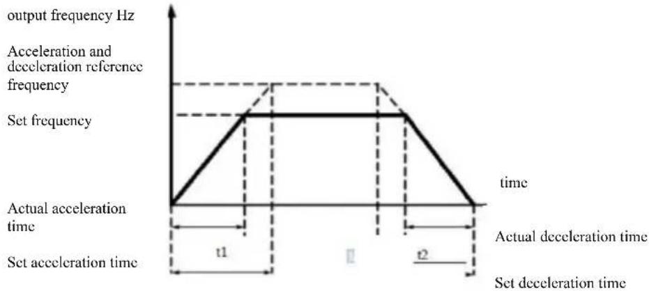
line
| Time Phase | Description | | ----------------------- | ------------------------------------- | | Start of output frequency | Output frequency Hz | | End of output frequency | Set frequency | | Start of actual acceleration time | Actual acceleration time | | End of actual deceleration time | Set deceleration time | | End of actual deceleration time | Actual deceleration time | | End of actual deceleration time | Set deceleration time |Figure 6-1 Diagram of acceleration and deceleration time
VFD provides four group of acceleration and deceleration time. Users can take advantage of the digital input terminal DI toggle. Four group of acceleration and deceleration time set by function code are as follows:
First group: P0-17, P0-18
Second group: P8-03, P8-04
second group: P8-05, P8-06
Fourth group: P8-07, P8-08
| P0-19 | Acceleration/Deceleration time unit | Factory default | 1 | |
| Setting range | 0 | 1s | ||
| 1 0.1s | ||||
| 2 0.01s | ||||
As to meet the needs of all types of site, VFD provides three kinds of acceleration and deceleration time units, respectively are 1 second, 0.1 seconds and 0.01 seconds.
Note: When modify the function parameters, Group 4 decimal places will change the displayed acceleration and deceleration time, Corresponding to the acceleration and deceleration time changes, pay special attention to the application process.
| P0-21 | Auxiliary superimposed frequency source bias frequency | Factory default | 0.0Hz |
| Setting range | 0.00Hz~maximum frequency F0-10 | ||
The function code is only valid when the frequency source selection is main and auxiliary calculation.
When the frequency source is the main and auxiliary calculation, P0-21, as an offset frequency, And primary and secondary operation are used as the final result of the superposition frequency setpoint to make the frequency setting more flexible.
| P0-22 | Resolution of frequency command | Factory default | 2 | |
| Setting range | 1 0.1Hz | |||
| 2 0.01Hz | ||||
This parameter is used to identify all frequency-dependent function code resolution.
When the frequency resolution is 0.1Hz when, VFD maximum output frequency can reach 3200Hz. When the frequency resolution is 0.01Hz, the maximum output frequency VFD is 600.00Hz.
Attention: When you modify the function parameters, all the parameters related decimal places of frequency will change. The corresponding frequency values shall also change, pay special attention when using.
| P0-23 | Digital setting frequency stop memoryselection | Factory default | 0 | |
| Setting range | 0 | No memory | ||
| 1 Memory | ||||
This function is only effective when the frequency source is set as numbers.
“No memory” means after inverter stops, digital set frequency value back to P0-08 (preset frequency) values. Keyboard ▲, ▼ keys or terminals UP, DOWN frequency correction performed is cleared. “Memory” means after inverter stops, digital set frequency reserved for the last stop time set frequency. Frequency keyboard ▲, ▼ keys or terminals UP, DOWN conduct correction remains valid.
| P0-24 | Motor selection | Factory default | 0 | |
| Setting range | 0 | Motor 1 | ||
| 1 | Motor 2 | |||
VFD supports drag-sharing drive 2 motors application. 2 motors can respectively set the motor nameplate, independent tuning parameters, choose a different control mode, independent setting performance related parameters and others.
Corresponding function parameter group of motor 1 is P1 group and P2 group. Corresponding function parameter group of motor 2 is A2 group.
The user to select current motor through P0-24 function code, you can also switch the motor through the input terminal DI digital. When the function code selection and terminal selection have contradiction, the terminal selection shall prevail.
| P0-25 | Acceleration/Deceleration time reference frequencies | Factory default | 0 | |
| Setting range | 0 | Maximum frequency (P0-10) | ||
| 1 | Set frequency | |||
| 2 100Hz | ||||
Acceleration and deceleration time means the acceleration and deceleration time from zero frequency to P0-25 setting frequency. Figure 6-1 is the Acceleration and Deceleration Time Schematic.
When P0-25 is selected as 1, deceleration time and frequency related to the set. If setting frequency change frequently, the motor acceleration is changable, so we need to pay attention to the application.
| P0-26 | Frequency command in operation UP/DOWN standard | Factory default | 0 | |
| Setting range | 0 | Operating frequency | ||
| 1 | Set frequency | |||
This parameter is valid only when the frequency source is digital setting.
When keyboard is used to determine the ▲, ▼ buttons or terminal UP/DOWN action, adopt any manner in which the frequency correction is set. That target frequency increases or decreases based on the operating frequency or based on the set frequency.
Difference between the two settings performs significantly when the inverter is in the process of acceleration and deceleration. That is, if the operating frequency and the set frequency of the inverter are not the same, the difference between different parameter selection will be large.
| P0-27 | Frequency source and command source in bundle | Factory default | 000 | |
| Setting range | Bit | Operation panel command binds frequency source | ||
| 0 | Unbound | |||
| 1 | Digital set frequency | |||
| 2 AI1 | ||||
| 3 AI2 | ||||
| 4 AI3 | ||||
| 5 | Digital set frequency | |||
| 6 | Multi-stage command | |||
| 7 | Simple PLC | |||
| 8 PID | ||||
| 9 | Communication given | |||
| Ten bit | Terminal command binds frequency source (0~9, same as bit) | |||
| Hundred bit | Communication command binds frequency source(0~9, same as bit) | |||
It defines the bundle of three run command channel and nine given frequencies between channels, and it is easy for the realization of synchronous switch.
The above frequencies given channel meaning is same with main frequency source X selection P0-03. See the description of function code P0-03. Different modes can be bundled with the same frequency given channel. When the command frequency source has bundled source, in the effective period of the command source, P0-03 \~ P0-07 set frequency source no longer works.
| P0-28 | Communication expansion card type | Factory default | 0 | |
| Setting range | 0 Modbus | communication card | ||
| 1 | Spare | |||
| 2 | Spare | |||
| 3 CANlink | communication card | |||
VFD provides two kinds of communication. This communication requires an optional communication card before use, and two kinds of communication can not be used at same time.
This parameter is used to set the type of the optional communication card. When the user to replace the communications card, you must set the parameters correctly.
P1 group: Parameters of 1^st motor
| P1-00 | Type selection of motor | Factory default | 0 | |
| Setting range | 0 | Common asynchronous motor | ||
| 1 | Variable frequency asynchronous motor | |||
| P1-01 | Rated power | Factory default | Depend on machine type | |
| Setting range | 0.1kW~1000.0kW | |||
| P1-02 | Rated voltage | Factory default | Depend on machine type | |
| Setting range | 1V~400V | |||
| P1-03 | Rated current | Factory default | Depend on machine type | |
| Setting range | 0.01A~655.35A (convertor power <=55kW)0.1A~6553.5A (convertor power >55kW) | |||
| P1-04 | Rated frequency | Factory default | Depend on machine type | |
| Setting range | 0.01Hz~max. frequency | |||
| P1-05 | Rated speed | Factory default | Depend on machine type | |
| Setting range | 1rpm~65535rpm | |||
The code for the motor nameplate parameters, both by VF control and vector control, are needed to accurately set the relevant parameters according to the motor nameplate.
In order to obtain better VF or vector control performance, the need for parameter tuning, and the accuracy of adjustment results, and properly set motor nameplate parameters closely.
| P1- | Stator resistance of asynchronous motor | Factory default | Depend on machine type |
| Setting range | 0.001Ω~30.000Ω | ||
| P1-07 | Rotor resistance of asynchronous motor | Factory default | Depend on machine type |
| Setting range | 0.001Ω~65.535Ω (convertor power <=55kW)0.0001Ω~6.5535Ω (convertor power>55kW) | ||
| P1-08 | Leakage inductive reactance of asynchronous motor | Factory default | Depend on machine type |
| Setting range | 0.01mH~655.35mH (convertor power <=55kW)0.001mH~65.535mH (convertor power >55kW) | ||
| P1-09 | Mutual inductive reactance of asynchronous motor | Factory default | Depend on machine type |
| Setting range | 0.1mH~6553.5mH (convertor power <=55kW)0.01mH~655.35mH (convertor power >55kW)) | ||
| P1-10 | No-load current of asynchronous motor | Factory default | Depend on machine type |
| Setting range | 0.01A~P1-03 (convertor power <=55kW)0.1A~P1-03 (convertor power >55kW) | ||
P1-06 \~ P1-10 is asynchronous motor parameters, these parameters generally do not have the motor nameplate, auto-tuning to get through the drive. Among them, “Induction Motor static tuning” can only get three parameters P1-06 \~ P1-08. But the “asynchronous motors complete tuning” can be obtained here except all five parameters, you can also get the encoder phase sequence, current loop PI parameters and others.
When changing motor rated power (P1-01) or the motor rated voltage (P1-02), the inverter will automatically modify the parameter value P1-06 \~ P1-10, and make these five parameters back to the usual standard Y series motor parameters.
If the site induction motor can not be tuned, you may according to the parameters provided by the manufacturer of the motor, input the corresponding function code.
| P1-27 | Encoder line number | Factory default | 1024 |
| Setting range | 1~65535 | ||
Setting ABZ encoder pulses per revolution.
In the case of speed sensorless vector control mode, you must set the correct number of encoder pulses, or the motor will not operate properly.
| P1-28 | Encoder type | Factory default | 0 | |
| Setting range | 0 | ABZ incremental encoder | ||
| 1 | Spare | |||
| 2 | Rotary transformer | |||
VFD supports multiple encoder types. Different encoders require matching different PG cards. Please choose the right PG card to use.
After installing the PG card, properly set P1-28 according to the actual situation, or the inverter may not operate properly.
| P1-30 | ABZ incremental encoder AB phase sequence | Factory default | 0 | |
| Setting range | 0 | Forward | ||
| 1 | Reverse | |||
This function code is only valid for the ABZ incremental encoder, which is only valid when P1-28 = 0. For setting phase sequence ABZ incremental encoder AB signal.
| P1-34 | Pole-pairs number of rotary transformer | Factory default | 1 |
| Setting range | 1~65535 | ||
Resolver is the number of pole pairs in the use of such an encoder, you must set the parameters number of pole pairs correctly.
| P1-36 | Speed feedback PG disconnection detection time | Factory default | 0.0s |
| Setting range | 0.0: no action 0.1s~10.0s | ||
It is used to establish encoder disconnection fault detection time, when set to 0.0s, the inverter will not detect encoder disconnection fault.
When the inverter detects a disconnection fault, and lasts longer than P1-36 set time, the inverter alarm ERR20.
| P1-37 | Tuning Selection | Factory default | 0 | |
| Setting range | 0 | No operation | ||
| 1 | Static tuning of asynchronous motor | |||
| 2 | Complete tuning of asynchronous motor | |||
0: No action, which prohibits tuning.
1: Asynchronous machine static tuning for induction motor and the load is not easy to disengage, but not a complete tuning occasion. Before conducting asynchronous static tuning, you must set the correct motor type and motor nameplate P1-00 \~ P1-05. Asynchronous machine static tuning, the inverter can be obtained P1-06 \~ P1-08 three parameters. Action description: Set the function code is 1, then press the RUN key, the inverter will conduct static tuning.
2: Asynchronous machine Complete tuning. As to ensure the dynamic control performance of the inverter, choose full tuning, the motor must be separated from the load to keep the motor for the no-load condition.
Complete tuning process, the inverter will conduct static tuning, and then follow the acceleration time to accelerate P0-17 to 80% of the motor rated frequency. After the holding period, P0-18 Deceleration according to the deceleration time and stop the tuning is performed before the asynchronous machine complete tuning. In addition to the need to set the motor type and motor nameplate parameters P1-00 \~ P1-05, but also need to set the correct encoder type and encoder pulses P1-27, P1-28. Asynchronous machine complete tuning, the drive can be obtained P1-06 \~ P1-10 five motor parameters and encoder AB phase sequence P1-30, vector control current loop PI parameters P2-13 \~ P2-16.
Action Description: Set the function code is 2, then press the RUN key, the inverter will complete tuning.
P2 group: Vector control parameters
Function code in P2 group is only effective for vector control, not for VF control.
| P2-00 | Speed loop proportional gain 1 | Factory default | 30 |
| Setting range | 1~100 | ||
| P2-01 | Speed loop integral time 1 | Factory default | 0.50s |
| Setting range | 0.01s ~10.00s | ||
| P2-02 | Switching frequency 1 | Factory default | 5.00Hz |
| Setting range | 0.00 ~F2-05 | ||
| P2-03 | Speed loop proportional gain 2 | Factory default | 15 |
| Setting range | 0~100 | ||
| P2-04 | Speed loop integral time 2 | Factory default | 1.00s |
| Setting range | 0.01s ~10.00s | ||
| P2-05 | Switching frequency 2 | Factory default | 10.00Hz |
| Setting range | F2-02 ~ Maximum output frequency | ||
Drive is running at different frequencies, you can select a different speed loop PI parameters. When operating frequency is smaller than the switching frequency 1 (P2-02), the speed loop PI adjustment parameters are P2-00 and P2-01. When the operating frequency is greater than the switching frequency 2, the speed loop PI adjustment parameters are P2-03 and P3-04. Speed loop PI parameters between switching frequency 1 and switching frequency 2 are the two group of PI parameters linear switching. Shown in Figure 6-2:
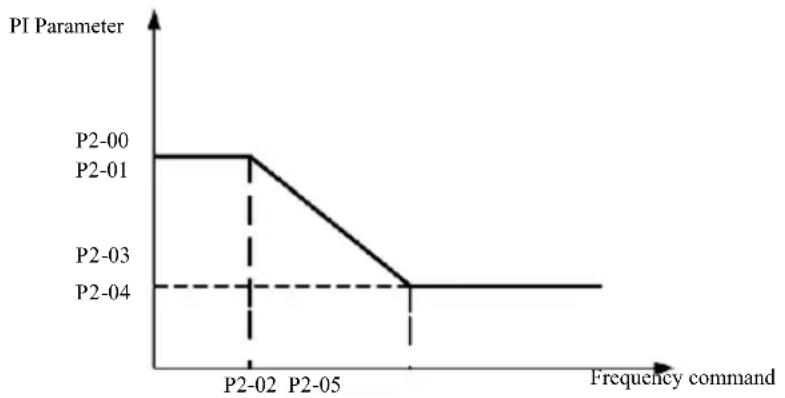
line
| Frequency command | PI Parameter | | :--- | :--- | | P2-00 | P2-01 | | P2-01 | P2-01 | | P2-03 | P2-03 | | P2-04 | P2-04 | | P2-05 | P2-05 |Figure 6-2 Diagram of PI parameters
Through setting the proportional coefficient of speed regulator and integration time, you can adjust vector control speed dynamic response characteristic.
Increasing the proportional gain, reducing the integration time can accelerate the dynamic response of the speed loop. However, the proportional gain is too large or the integral time too small may cause the system to vibrate. Recommend adjustment method:
If the factory parameters can not meet the requirements, then the value of the parameter in the factory on the basis of fine-tuning. Increase the proportional gain first to ensure that the system does not oscillate; then decrease the integration time, the system has quick response characteristics and small overshoot.
Note: As PI parameters are set incorrectly, it may cause large overshoot speed. Even when students fall overshoot overvoltage fault.
| P2-06 | Vector control slip gain | Factory | 100% |
| Setting range | 50%~200% | ||
Speed sensorless vector control This parameter is used to adjust the steady speed precision motor: When the motor load is low to increase the speed parameter, vice versa.
For speed sensor vector control, this parameter can also adjust the load of the inverter output current.
| P2-07 | Speed loop filter time | Factory | 0.000s |
| Setting range | 0.000s ~0.100s | ||
In vector control mode, the speed loop regulator output torque current command, the parameters for the torque command filter. This parameter is generally no need to adjust the speed fluctuations that may be appropriate to increase the filtering time; If the motor oscillation occurs, it should be appropriate to reduce this parameter.
Speed loop filter time constant is small, the output torque of the drive may be volatile, but the response speed is fast.
| P2-08 | Vector control over | Factory | 64 |
| Setting range | 0~200 | ||
During the deceleration, the over-excitation control bus voltage rise can be suppressed to avoid overvoltage fault. Greater the over excitation gains, stronger the suppression has effect.
For conditions that in the inverter deceleration process, it is easier to be over-pressured and sounds alarm, you need to improve the over excitation gain. But if excitation gain is too large, easily lead the output current to increase; you need to weigh in the application.
For the case of small inertia, deceleration of the motor voltage rise does not appear, it is recommended that the over excitation gain is 0; For braking resistance of the occasion, it is also suggested that over-excitation gain is set to 0.
| P2-09 | Speed control mode torque limit source | Factory default | 0 | |
| Setting range | 0 | F2-10 | ||
| 1 | AI1 | |||
| 2 | AI2 | |||
| 3 | AI3 | |||
| 4 | PULSE Setting | |||
| 5 | Communication Preferences | |||
| P2-10 | Torque limit speed control mode digital set | Factory default | 150.0% | |
| Setting range | 0.0%~200.0% | |||
In speed control mode, the maximum value of the inverter output torque is controlled by the torque limit source.
P2-09 is used to select the source to set the speed limit, when the via analog, pulse, communication settings, 100% corresponds to the appropriate setting P2-10, P2-10 and 100% of the inverter rated torque.
| P2-13 | Excitation regulator proportional gain | Factory default | 2000 |
| Setting range | 0~20000 | ||
| P2-14 | Excitation regulation integral gain | Factory default | 1300 |
| Setting range | 0~20000 | ||
| P2-15 | Torque control proportional gain | Factory default | 2000 |
| Setting range | 0~20000 | ||
| P2-16 | Torque control integral gain | Factory default | 1300 |
| Setting range | 0~20000 | ||
Vector control current loop PI adjustment parameters. The complete tuning parameters in an asynchronous machine or synchronous machine will automatically load after tuning, generally do not need to modify.
What needs to be reminded is that the current loop integral controller, instead of using the integration time as a dimension, but directly set the integral gain. PI current loop gain is set too high, it may cause the entire control loop oscillation, so when current oscillations or torque ripple is large, it can be reduced manually for PI proportional gain or integral gain here.
P3 group-V/F control parameters
The function code only for V / F control is effective. For vector control, it is invalid.
V / F control is suitable for fans, pumps and other general load, or a inverter with multiple motors, or inverter power and motor power quite different applications.
| P3-00 | V/F curve setting | Factory default | 0 | |
| Setting range | 0 | Straight lineV / F | ||
| 1 | MoreV / F | |||
| 2 | SquareV / F | |||
| 3 | 1.2 times V / F | |||
| 4 | 1.4 times V / F | |||
| 6 | 1.6 times V / F | |||
| 8 | 1.8 times V / F | |||
| 9 | Retention | |||
| 10 | VF Complete separation mode | |||
| 11 | VF Semi-separation mode | |||
0: Linear V / F. Suitable for ordinary constant torque load.
1: Multi-point V / F. Suitable for dehydration machines, centrifuges and other special loads. At this time by setting P3-03 \~ P3-08 parameters, it can be obtained at any of VF curve.
2: Multi-point V / F. Suitable for fans, pumps and other centrifugal load.
3\~8: VF curve between the straight line between the PF and VF square.
10: VF completely separate mode. Then the output frequency of the inverter output voltage independent of each other, the output frequency is determined by the frequency source. But output voltage is determined by P3-13 (VF isolated voltage source).
VF complete separation mode, Generally used in induction heating, power inverter, torque motor control and other applications.
11: VF semi-separation mode.
In this case V and F are proportional, but proportional to the voltage source by setting P3-13, and the relationship between V and F are also group P1 rated motor voltage related to the rated frequency.
Suppose the input voltage source is X (X is 0 to 100% of the value), the output voltage V F of the relationship between the inverter and the frequency is:
V / F=2*X* (Motor rated voltage) / (rated motor frequency)
| P3-01 | Torque boost | Factory default | Model confirmation |
| Setting range | 0.0%~30% | ||
| P3-02 | Cut-off frequency of torque | Factory default | 50.00Hz |
| Setting range | 0.00Hz~maximum output frequency | ||
As to compensate for V / F control low frequency torque characteristics, make increase compensation for the low-frequency inverter output voltage. However, the torque boost is set too large, the motor overheating, inverter over-current.
When the load is heavy and the motor starting torque is not enough, it is recommended to increase this parameter. Light can be reduced when the load torque boost. When the torque boost is set to 0.0, the inverter is automatic torque boost, torque boost at this time according to the drive motor stator resistance parameters calculated automatically required.
Torque boost Torque cut-off frequency: Under this frequency, torque boost torque is effective. More than this set frequency, torque boost will failure. See details in Figure 6-3.
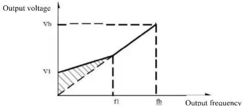
line
| Output frequency | Output voltage | | ---------------- | -------------- | | V1 | V1 | | Vb | Vb |VI: Manual torque boost voltage
Vb: Maximum output voltage
fl: Manual torque boost cut-off frequency fb: Rated operating frequency
Figure 6-3 Diagram of manual torque boost
| P3-03 | Multi-VF frequencies F1 | Factory default | 0.00Hz |
| Setting range | 0.00Hz~P3-05 | ||
| P3-04 | Multi-VF Voltage point V1 | Factory default | 0.0% |
| Setting range | 0.0%~100.0% | ||
| P3-05 | Multi-VF frequencies F2 | Factory default | 0.00Hz |
| Setting range | P3-03~P3-07 | ||
| P3-06 | Multi-VF Voltage point V2 | Factory default | 0.0% |
| Setting range | 0.0%~100.0% | ||
| P3-07 | Multi-VF frequencies F3 | Factory default | 0.00Hz |
| Setting range | P3-05 ~ motor rated frequency (P1-04) Note:second motor rated frequency is A2-04 | ||
| P3-08 | Multi-VF Voltage point V3 | Factory default | 0.0% |
| Setting range | 0.0%~100.0% | ||
P3-03 \~ P3-08 six parameters to define multi-segment V / F curve.
Multi-point curve V / F should be set according to the load characteristics of the motor. What need to be aware of is that, Relationship between the voltage and frequency three points points must be met: V1 < V2 < V3, F1 < F2 < F3. Figure 6-4 is a schematic view of multi-point setting VF curve.
Voltage is set too high may cause motor overheating and even burned at low frequencies, the drive may be too stall or over-current protection.
| P3-09 | VF slip compensation gain | Factory default | 0 |
| Setting range | 0%~200.0% | ||
VF Slip compensation. It can be compensated induction motor generated when the load increases the motor speed deviation when the load changes the motor speed can be stable.
VF Slip compensation gain is set to 100.0%, indicating that slip when the motor with a rated load compensation to the motor rated slip. But the motor rated slip, the drive motor rated frequency group by P1 and rated speed to get own calculations.
Adjust VF rpm slip compensation gain, generally when the rated load, the motor speed and the target speed is substantially the same as the principle. When the motor speed and the target value is not the same, you need to be properly fine-tune the gain.
| P3-10 | VF over excitation gain | Factory default | 6 |
| Setting range | 0~200 | ||
During the deceleration, the over-excitation control bus voltage rise can be suppressed to avoid overvoltage fault. Greater the over excitation gains, stronger the suppression has effect.
For conditions that in the inverter deceleration process, it is easier to be over-pressured and sounds alarm, you need to improve the over excitation gain. But if excitation gain is too large, easily lead the output current to increase; you need to weigh in the application.
For the case of small inertia, deceleration of the motor voltage rise does not appear, it is recommended that the over excitation gain is 0; For braking resistance occasion, it is also suggested that over-excitation gain is set to 0.
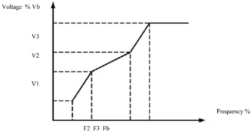
line
| Frequency (%) | Voltage % Vb | | :--- | :--- | | F2 | V1 | | F3 | V2 | | Fb | V3 |V1-V3: Multi-speed V / F voltage percentage of segment 1-3
F1-F3: Multi-speed V / F frequency percentage of segment 1-3
Vb: Motor rated voltage Fb: motor rated operating frequency
Figure 6-4 Diagram of multi-point V / F curve setting
| P3-11 | VF oscillation suppression gain | Factory default | Model confirmation |
| Setting range | 0~100 | ||
The gain selection method is effective in suppressing oscillation, try to take small, so as not to adversely affect the VF operation. When the motor has no oscillation, select this gain as 0. Only when the motor has obvious oscillation only be appropriate to increase the gain, the greater the gain, the oscillation suppression result.
When using the oscillation suppression function requires the motor rated current and no-load current parameters to be accurate, or VF oscillation suppressing effect is not good.
| P3-13 | VF Isolated voltage | Factory default | 0 | |
| Setting range | 0 | Digital setting (P3-14) | ||
| 1 AI1 | ||||
| 2 AI2 | ||||
| 3 AI3 | ||||
| 4 | Pulse setup (D15) | |||
| 5 | Multi-step instructions | |||
| 6 | Simple PLC | |||
| 7 PID | ||||
| 8 | Communication given | |||
| 100.0% Corresponds to the motor rated voltage (P1-02, A4-02, A5-02, A6-02) | ||||
| P3-14 | VF isolated digital voltage setting | Factory default | 0V | |
| Setting range | 0V ~ motor rated voltage | |||
VF separation generally used in induction heating, power inverter and torque motor control applications. When choosing VF separation control, the output voltage can be set by function code P3-14, but also from analog, multi-instruction, PLC, PID or communication given. When set to a non-digital, each set corresponding to 100% of rated voltage of the motor, when the percentage of the absolute value of the analog output setting, etc. is negative. So places is set as an active setpoint.
0: Digital setting (P3-14) voltage is directly set by P3-14.
1: AI1 2: AI2 3: AI3
Voltage from the analog input terminal to determine.
-
Pulse setup (DI5) given via the terminal voltage pulse given. Pulse reference signal specification: voltage range 9V \~ 30V, frequency range 0kHz \~ 100kHz.
-
When multi-source voltage instruction multistage instruction, set the group P4 PC and set parameters to determine if a given signal and the reference voltage correspondence.
-
Simple PLC
When the voltage source is simple PLC, need to set the PC set of parameters to determine if a given output voltage.
- PID
According to PID closed loop generates an output voltage. See details PA group PID introduction.
- Communication refers to the voltage given by the host computer via the communication mode. When the voltage source selection 1-8, 0 corresponds to 100% of the output voltage of 0V motor rated voltage.
| P3-14 | VF isolated voltage rise time | Factory default | 0.0s |
| Setting range | 0.0s~1000.0s | ||
VF separation rise time refers to the output voltage changes from 0V to rated motor voltage required time. Shown in Figure 6-5:
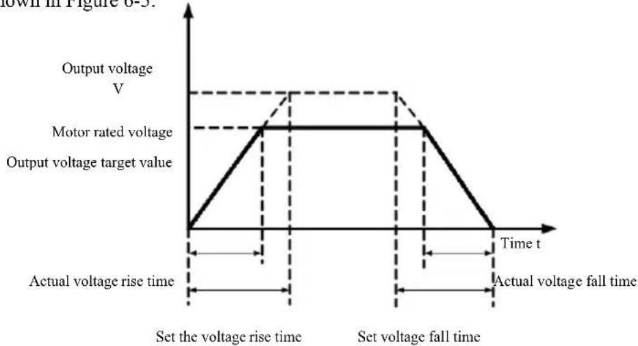
line
| Time t | Output voltage V | Actual voltage rise time | | ------ | ---------------- | ------------------------ | | Start | 0 | 0 | | Mid | 1 | 0 | | Peak | 1 | 0 | | End | 0 | 0 |Figure 6-5 Diagram of V/F separation
P4 group: Input termianl
This series inverter comes standard with five multifunctional digital input terminals (Where DI5 can be used as high-speed pulse input terminal). Two analog input terminals. If the system needs more input and output terminals can be optional multifunctional input and output expansion card.
Multi-function input and output expansion card has five multifunctional digital input terminals (DI6\~DI10), An analog input terminal (AI3).
| P4-00 | DI1Terminal function selection | Factory default | 1 (running) |
| P4-01 | DI2Terminal function selection | Factory default | 4 (positive turning point move) |
| P4-02 | DI3Terminal function selection | Factory default | 9 (fault reset) |
| P4-03 | DI4Terminal function selection | Factory default | 12 (multi speed 1) |
| P4-04 | DI5Terminal function selection | Factory default | 13 (multi speed 2) |
| P4-05 | DI6Terminal function selection | Factory default | 0 |
| P4-06 | DI7Terminal function selection | Factory default | 0 |
| P4-07 | DI8Terminal function selection | Factory default | 0 |
| P4-08 | DI9Terminal function selection | Factory default | 0 |
| P4-09 | DI10Terminal function selection | Factory default | 0 |
These parameters are used to set the digital multi-function input terminal functions can be selected functions as follows:
| Set point | Function | Explanation |
| 0 | No function | The terminal will not be used to “No function” to prevent malfunction. |
| 1 | Forward running (FWD) | By external terminal to control forward and reverse drive. |
| 2 | Reverse running (REV) | |
| 3 | Three-wire run control; | This terminal is used to determine the inverter operating mode is a three-line control mode. For details, see function code P4-11 (“terminal command mode”) instructions. |
| 4 | Forward jog (FJOG) | JOG jog forward running, JOG jog reverse running. Jog frequency jog acceleration and deceleration time refer to the function code P8-00, P8-01, P8-02 description. |
| 5 | Turning points (RJOG) | |
| 6 | Terminals UP | By external terminals a given frequency modification frequency increment, decrement instruction. Frequency source is set to digital setting, can be adjusted up and down to set the frequency. |
| 7 | Terminal DOWN | |
| 8 | Free stoppage | Inverter blocks the output, then stop the process from motor inverter control. This way is same with freewheel meaning of the P6-10. |
| 9 | Reset (RESET) | Use terminal fault reset function. And RESET function key on the keyboard. This function is used to implement remote fault reset. |
| 10 | Pause operation | The inverter is stopped, but all operating parameters are memories. Parameters such as PLC, Wobble parameters, PID parameters. After this terminal signal disappears, the drive back to the state before stopping the run. |
| 11 | External fault normally open input | When this signal is sent to the inverter, the inverter reports fault ERR15, troubleshooting and fault protection according to the operation mode (for details to participate in the function code P9-47). |
| 12 | Multi-speed terminal 1 | By 16 states of the four terminals for speed or 16 other instruction set. 16. for details, see Table 1. |
| 13 | Multi-speed terminal 2 | |
| 14 | Multi-speed terminal 3 | |
| 15 | Multi-speed terminal 4 | |
| 16 | Deceleration time selection terminal 1 | This four states two terminals, four options to achieve acceleration and deceleration time, for details, see Table 2. |
| 17 | Deceleration time selection terminal 2 | |
| 18 | Frequency source switching | As to switch to select a different frequency source.According to the frequency source selection function code (P0-07) is set when a set between the two frequencies as the source switching frequency source, this terminal is used to switch between two frequency source. |
| 19 | UP / DOWN Setting clear (terminal, keyboard) | When the frequency of a given digital frequency reference, this terminal can clear frequency terminal UP / DOWN keyboard or UP / DOWN changed, so that a given frequency back to the set value of P0-08. |
| 20 | Running command switching terminal | When the command source is set to terminal control (P0-02 = 1), this terminal can be switched terminal control and keyboard control.When the command source is set to the communication control (P0-02 = 2), this terminal can be switched communication control and keyboard control. |
| 21 | Ramp stop Ensure that the drive is not external signals (except stop command), to maintain the current output frequency. | |
| 22 | PID Time out | PID is temporarily disabled, the inverter maintains the current frequency output, no longer frequency source PID adjust. |
| 23 | PLC State reset | PLC pause in the implementation process, is running again, you can restore the inverter through this terminal to the initial state of simple PLC. |
| 24 | Swing frequency pause Drive to the center frequency output. Wobble function pause. | |
| 25 | Counter input Count input terminal of the pulse. | |
| 26 | Counter reset Counter clearing processing status. | |
| 27 | Length count input Length count input terminal. | |
Specification of high-performance vector convertor
Parameter description
| Set point | Function | Explanation |
| 28 | Length reset Length clear | |
| 29 | Torque control disabled Prohibit the drive torque control, the inverter goes into the speed control mode | |
| 30 | Pulse (pulse) frequency input (valid only for DI5) | DI5 as a pulse input terminal functions. |
| 31 | Retention Retention | |
| 32 | Now the DC braking | When this terminal is valid, inverter switching directly to the DC braking state |
| 33 | External fault normally closed input | When the normally closed external fault signal into the inverter, the inverter reports fault ERR15 and downtime. |
| 34 | Frequency modification enabled | If this function is set to valid, when the frequency is changed, the drive does not respond to change frequency, until the terminal state is invalid. |
| 35 | PID action direction takes opposite direction | When this terminal is valid, PID action direction and the direction opposite to the set PA-03 |
| 36 | Exterior stoppage Terminal 1 | When conducting keyboard control, this terminal can be used to stop the inverter, the STOP key on the keyboard equivalent functions. |
| 37 | Control command switching terminal 2 | For switching between the terminal control and communication control. If the command source is selected as terminal control, the system switches to the communication terminal effective control; Vice versa. |
| 38 | PID Points pause | When this terminal is valid, the PID integral regulation pause, but the proportion of PID regulation and differential regulation is still valid. |
| 39 | Frequency source X and preset frequency switching | The terminal is enabled, the frequency source X with preset frequency (P0-08) Alternative |
| 40 | Frequency source Y and preset frequency switching | The terminal is enabled, the frequency source Y with preset frequency (P0-08) Alternative |
| 41 | Motor selection terminal 1 | Those two states by two terminals, two sets of motor parameters can switch, for details, see Table 3. |
| 42 | Motor selection terminal 2 | |
| 43 | PID Parameter switch | When PID parameter switching conditions for the DI terminal (PA-18 = 1), this terminal is invalid, PID parameter PA-05 ~ PA-07; PA-15 is used when the terminal is valid ~ PA-17; |
| 44 | User-defined fault 1 | User-defined fault 1 and 2 are valid, the inverter respectively alarm ERR27 and ERR28, the drive will select P9-49 selected operation mode processing based fault protection action. |
| 45 | User-defined fault 2 | |
| 46 | Speed control / torque control switch | Between the drive torque control and speed control modes. The terminal is invalid, A0-00 (speed / torque control) mode is defined in the drive is running, the terminal is valid and then switches to another mode. |
| 47 | Emergency Shutdown | When this terminal is valid, the drive with the fastest speed parking, parking during the current limit in the current set. This function is used to meet when the system is in a state of emergency, the drive needs to stop as soon as possible requirements. |
| 48 | Exterior stoppage Terminal 2 | In any control mode (the control panel, terminal control, communication control), the terminal can be used to make the inverter is stopped, then the deceleration time is fixed deceleration time 4. |
| 49 | DC braking deceleration | When this terminal is valid, the inverter will decelerate to stop DC braking starting frequency, and then switch to the DC braking. |
| 50 | The running time is cleared | When this terminal is valid, inverter operation timing of this time is cleared, this feature requires the timed run (P8-42) and run this time is reached (P8-53) with the use. |
Annexed Table 1 Multi-section Instruction's Function Description
More than four segments command terminal, it can be combined into 16 states. Each state corresponds to the 16 16 instruction set values. Specifically as shown in Table 1:
| K_4 | K_3 | K_2 | K_1 | Instruction set | Corresponding parameters |
| OFF OFF | OFF OFF | Multi segment instruction 0 | PC-00 | ||
| OFF OFF | OFF ON | Multi segment instruction 1 | PC-01 | ||
| OFF OFF | ON OFF | Multi segment instruction 2 | PC-02 | ||
| OFF OFF | ON ON | Multi segment instruction 3 | PC-03 | ||
| OFF ON | OFF OFF | Multi segment instruction 4 | PC-04 | ||
| OFF ON | OFF ON | Multi segment instruction 5 | PC-05 | ||
| OFF ON | ON OFF | Multi segment instruction 6 | PC-06 | ||
| OFF ON | ON ON | Multi segment instruction 7 | PC-07 | ||
| ON OFF | OFF OFF | Multi segment instruction 8 | PC-08 | ||
| ON OFF | OFF ON | Multi segment instruction 9 | PC-09 | ||
| ON OFF | ON OFF | Multi segment instruction 10 | PC-10 | ||
| ON OFF | ON ON | Multi segment instruction 11 | PC-11 | ||
| ON ON | OFF OFF | Multi segment instruction 12 | PC-12 | ||
| ON ON | OFF ON | Multi segment instruction 13 | PC-13 | ||
| ON ON | ON OFF | Multi segment instruction 14 | PC-14 | ||
| ON ON | ON ON | Multi segment instruction 15 | PC-15 | ||
When the frequency source selection for the multispeed function code PC-00 \~ PC-15 of 100.0%, corresponding to the maximum frequency P0-10. Multi-step instructions except as a multi-speed function, but also can be used as PID given source, or as a voltage source VF separation control, etc., to meet the needs of different between a given value in switching.
Annexed Table 2 Acceleration and deceleration time selection terminal functions
| Terminal 2 | Terminal 1 | Acceleration or deceleration time selection Corresponding | |
| OFF OFF | Acceleration time 1 | P0-17、P0-18 | |
| OFF | ON | Acceleration time 1 | P8-03、P8-04 |
| ON OFF | Acceleration time 3 | P8-05、P8-06 | |
| ON | ON | Acceleration time 4 | P8-07、P8-08 |
Annexed Table 3 Motor selection Terminal functions
| Terminal 2 | Terminal 1 | Motor selection Corresponding parameter set | |
| OFF | OFF | Motor 1 | P1, P2 Group |
| OFF ON | Motor 2 | A2 Group | |
| P4-10 | DI filtering time | Factory | 0.010s | |
| Setting | 0.000s~1.000s | |||
Setting DI status of the terminal software filter time. If you are using the occasion input terminal susceptible to interference caused by malfunction of this parameter can be increased in order to enhance the anti-jamming capability. While this increases filter time can cause slow response DI terminal.
| P4-11 | Terminal command mode | Factory default | 0 | ||
| Setting range | 0 | Two-wire 1 | |||
| 1 | Two-wire 2 | ||||
| 2 | Three-wire 1 | ||||
| 3 | Three-wire 2 | ||||
This parameter defines the external terminal through the inverter to control the operation of four different ways.
0: Two-wire mode 1: This mode is the most commonly used two-line mode. By the terminal D11, D12 to determine the motor forward and reverse operation.
Terminal function set as follows:
| Terminals | Set point | Description |
| DI1 | 1 | Forward running (FWD) |
| DI2 | 2 | Reverse running (REV) |
Wherein, D11, D12 are multi-function input terminal of D11 \~ D110, the level is effective.
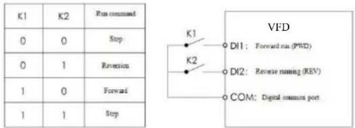
Figure 6-6 Two-line mode 1
1: Two-wire mode 2: Use this mode when DI1 terminal function operation enable terminal and DI2 terminal function to determine the direction.
Terminal function set as follows:
| Terminals | Set point | Description |
| DI1 | 1 | Forward running (FWD) |
| DI2 | 2 | Reverse running (REV) |
Where in, DI1, DI2 are multi-function input terminal of DI1 \~ DI10, the level is effective.
Figure 6-7 Two-line mode 2
Parameter description
Specification of high-performance vector convertor
2: Three-wire control mode 1: This mode is enabled terminal DI3, respectively, by direction DI1, DI2 control.
| Terminals | Set point | Description |
| DI1 | 1 Forward running (FWD) | |
| DI2 | 2 | Reverse running (REV) |
| DI3 | 3 | Three-wire run control |
When there is the need to run, the terminal must first DI 3 closed by the rising edges of the DI1 or DI2 to achieve forward or reverse motor control.
When you need to stop, by disconnecting DI3 terminal shall signal to achieve. Wherein, DI1, DI2, DI3 are multifunctional input terminals of DI1 \~ DI10, DI1, DI2 pulse are effective, DI3 is effective level.
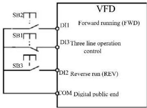
flowchart
graph TD
    A["SB2"] --> B["DI1 Forward running (FWD)"]
    C["SB1"] --> D["DI3 Three line operation control"]
    E["SB3"] --> F["DI2 Reverse run (REV)"]
    G["COM"] --> H["Digital public end"]
Figure6-8 Three wire control mode 1
Among :
SB1: stop button SB2: Forward button SB3: reverse button
3: Three-line control mode 2: This mode enable terminal to DI 3, run the command given by the DI1, DI2 direction by the state to decide.
Terminal function is set as follows :
| Terminals | Set point | Description |
| DI1 | 1 Forward running | |
| DI2 | 2 | Reverse running (REV) |
| DI3 | 3 | Three-wire run control |
In the need to run, must first close the DI3 terminal, from the DI1 of the pulse rise along the motor running signal, DI2 state of the motor direction signal.
In the need to stop, it is required to disconnect the DI3 terminal signal to achieve. Among them, DI1, DI2, DI3 for the DI1 \~ DI10 multi function input terminals, DI1 for the pulse effective, DI3, DI2 is effective.
| K | Running direction |
| 0 | Forward |
| 1 | REV |
flowchart
graph TD
    A["SB2"] --> B["DI1"]
    C["SB1"] --> D["DI3"]
    E["K"] --> F["DI2"]
    B --> G["Forward running (FWD)"]
    D --> H["Three line operation control"]
    F --> I["Reverse run(REV)"]
    G --> J["VFD"]
    H --> J
    I --> J
    J --> K["COM digital public end"]
Figure6-9 Three wire control mode 2
Among them: SB1: stop button SB2: run the button
| P4-12 | Terminal UP / DOWN rate of Setting | Factory default 1.00Hz/s |
| 0.01Hz/s~65.535Hz/s |
When setting terminal UP / DOWN adjust set frequency, the frequency rate of change, that is, the amount of change in frequency per second.
When P0-22 (frequency decimal point) is 2, the value is in the range of 0.001Hz / s \~ 65.535Hz / s.
When P0-22 (frequency decimal point) is 1, the value is in the range of 0.01Hz / s \~ 655.35Hz / s.
| P4-13 | Al curve 1 Minimum InputSetting 0.00V~P4-15 | Factory default | 0.00V |
| P4-14 | AI curve 1 minimum input corresponding settings | Factory default | 0.0% |
| Setting -100.00%~100.0% | |||
| P4-15 | AI curve 1 maximum inputSetting P4-13~10.00V | Factory default | 10.00V |
| P4-16 | AI curve 1 maximum input corresponding to set | Factory default | 100.0% |
| Setting -100.00%~100.0% | |||
| P4-17 | AI1 filtering timeSetting 0.00s~10.00s | Factory default | 0.10s |
The above function codes are used to set the analog input voltage setpoint relationship between its representatives.
When the analog input voltage is greater than the set “maximum input” (P4-15), the analog voltage in accordance with the “maximum input” computing; similarly, when the analog input voltage is less than the set “minimum input” (P4-13), according to “AI is below the minimum input setting Select” (P4-34) is set to the minimum input or 0.0% calculated.
When the analog input is current input, 1mA current corresponds to 0.5V.
AI1 input filtering time for setting AI1 software filtering time when the analog easily disturbed site, please increase the filter time so that the analog detection stabilized, but the greater the filtering time of the analog detection slow response times, how to set up a trade-off depending on the application.
In different applications, analog setting 100.0% of the nominal value of the corresponding meanings vary, please refer to the description of each part of the application.
The following illustrates a case where two typical settings :
Figure6-10 The corresponding relationship between the simulation and the set amount
| P4-18 | AI curve 2 minimum input | Factory default | 0.00V | |
| Setting range | 0.00V~P4-20 | |||
| P4-19 | AI curve 2 minimum input corresponding settings | Factory default | 0.0% | |
| Setting range | -100.00%~100.0% | |||
| P4-20 | AI curve 2 maximum input | Factory default | 10.00V | |
| Setting range | P4-18~10.00V | |||
| P4-21 | AI curve 2 maximum input corresponding to set | Factory default | 100.0% | |
| Setting range | -100.00%~100.0% | |||
| P4-22 | AI2 filtering time | Factory default | 0.10s | |
| Setting range | 0.00s~10.00s | |||
Function and use of curve 2, please refer to the description of the curve 1.
| P4-23 | AI curve 3 minimum input | Factory default | 0.00V | |
| Setting range | 0.00s~P4-25 | |||
| P4-24 | AI curve 3 minimum input corresponding settings | Factory default | 0.0% | |
| Setting range | -100.00%~100.0% | |||
| P4-25 | AI curve 3 maximum input | Factory default | 10.00V | |
| Setting range | P4-23~10.00V | |||
| P4-26 | AI curve 3 maximum input corresponding to set | Factory default | 100.0% | |
| Setting range | -100.00%~100.0% | |||
| P4-27 | AI3 filtering time | Factory default | 0.10s | |
| Setting range | 0.00s~10.00s | |||
Function and use of curve 3, please refer to the description of the curve 1.
| P4-28 | PULSE minimum input | Factory default | 0.00kHz | |
| Setting range | 0.00kHz~P4-30 | |||
| P4-29 | PULSE minimum input correspondence | Factory default | 0.0% | |
| Setting range | -100.00%~100.0% | |||
| P4-30 | PULSE maximum input | Factory default | 50.00kHz | |
| Setting range | P4-28~50.00kHz | |||
| P4-31 | PULSE maximum input correspondence | Factory default | 100.0% | |
| Setting range | -100.00%~100.0% | |||
| P4-32 | PULSE filtering time | Factory default | 0.10s | |
| Setting range | 0.00s~10.00s | |||
This function code is used to set the relationship DI5 pulse frequency corresponding to the set between.
Pulse frequency inverter can only be entered through DI5 channel. Application and function curve of this group is similar to 1, please refer to Note 1 of the curve.
| P4-33 | AI curve selection | Factory default | 321 | ||
| Setting range | Single digit | AI1 curve selection | |||
| 1 | Curve 1 (2 points, see P4-13 ~ P4-16) | ||||
| 2 | Curve 2 (2 points, see P4-18 ~ P4-21) | ||||
| 3 | Curve 3 (2 points, see P4-23 ~ P4-26) | ||||
| 4 | Curve 4 (4 points, see A6-00 ~ A6-07) | ||||
| 5 | Curve 5 (4 points, see A6-08 ~ A6-15) | ||||
| Ten bit | AI2 curve selection (1 ~ 6, the same as above) | ||||
| Hundred bit | AI3 curve selection (1 ~ 6, the same as above) | ||||
The function code bits, ten, one hundred are used to select, analog input AI1, AI2, AI3 corresponding setting curve. 3 analog inputs can be selected in any of the five kinds of curve a.
Curve 1, curve 2, curve 3 are 2 point curve, set in P4 group function code, whereas curve 4 and curve 5 are 4 point curve, you need to set the A8 group function codes.
This inverter standard unit provides two analog inputs, AI3 must be configured to use multi-function input and output expansion card.
| P4-34 | AI is below the minimum input setting | Factory default | 000 | ||
| Setting range | Single digit | AI1 lower than the minimum input settings select | |||
| 0 | Corresponding minimum input setting | ||||
| 1 0.0% | |||||
| Ten bit | AI2 lower than the minimum input settings selected (0 ~ 1, above) | ||||
| Hundred bit | AI3 lower than the minimum input settings selected (0 ~ 1, above) | ||||
The function code is used to set, when the analog input voltage is less than the set “minimum input”, the corresponding analog set how to determine.
The function code unit, ten bit, hundred bit, corresponding to the analog input AI1, AI2, AI3. If this option is 0. When the AI input below the “minimum input”, corresponding to the analog setting function code to determine the curve “minimum input corresponds to a given” (P4-14, P4-19, P4-24).
If this option is 1, then when AE input below the minimum input, the analog corresponding to 0.0%.
| P4-35 | DI1 delay time | Factory default | 0.0s | |
| Setting | 0.0s~3600.0s | |||
| P4-36 | DI2 delay time | Factory default | 0.0s | |
| Setting | 0.0s~3600.0s | |||
| P4-37 | DI3 delay time | Factory default | 0.0s | |
| Setting | 0.0s~3600.0s | |||
When DI terminal for setting status changes, they are changes in the delay time of the inverter. Currently only DI1, DI2, DI3 have set the time delay function.
| P4-38 | DI terminal effective mode selection 1 | Factory default | 00000 | ||
| Setting range | Single digit | DI1 terminal active set | |||
| 0 | Active High | ||||
| 1 | Active Low | ||||
| Ten bit | DI2 Terminal active set (0-1, supra) | ||||
| Hundred bit | DI3 Terminal active set (0-1, supra) | ||||
| Thousand bit | DI4 Terminal active set (0-1, supra) | ||||
| Ten thousand bit | DI5 Terminal active set (0-1, supra) | ||||
| P4-39 | DI terminal effective mode selection 2 | Factory default | 00000 | ||
| Setting range | Single digit | DI6 terminal active set | |||
| 0 | Active High | ||||
| 1 | Active Low | ||||
| Ten bit | DI7 Terminal active set (0-1, supra) | ||||
| Hundred bit | DI8 Terminal active set (0-1, supra) | ||||
| Thousand bit | DI9 Terminal active set (0-1, supra) | ||||
| Ten thousand bit | DI10 Terminal active set (0-1, supra) | ||||
It is used for setting the digital input terminal of the active mode. When choosing high effective, the corresponding S terminal and COM communicated effectively, disconnect invalid. Selected as active low, the corresponding S terminal and COM connectivity invalid, effectively disconnected.
P5 Group--Output terminals
This series inverter comes standard with a multifunction analog output terminal, a multi-function digital output terminal, a multi-function relay output terminal, an FM terminal (selected as high-speed pulse output terminal, can also choose a set open switch electrode output). As the output terminal can not meet the site with app, you need the optional multi-function input and output expansion card.
Multi-function input and output expansion card output terminals, comprising a multi-function analog output terminal (AO2), 1 multifunction relay output terminal (relay 2), a multi-function digital output terminal (DO2).
| P5-00 | FM terminal output mode selection | Factory default | 0 | ||
| Setting range | 0 | Pulse output (FMP) | |||
| 1 | Switching output (FMR) | ||||
FM terminal is a programmable multiplexing terminal can be used as high-speed pulse output terminal (FMP), the switch can also be used as open collector output terminal (FMR).
As the pulse output FMP, the maximum output pulse frequency is 100kHz, FMP-related functions can be found P5-06 instructions.
| P5-01 | FMRI function selection (open collector output terminal) | Factory default | 0 |
| P5-02 | Relay output function selection (T / A-T / B-T / C) | Factory default | 2 |
| P5-03 | Expansion card relay output function selection (P / A-P / B-P / C) | Factory default | 0 |
| P5-04 | DO1 output function selection (open collector output terminal) | Factory default | 1 |
| P5-05 | Expansion card DO2 output function selection | Factory default | 4 |
The five function code is used to select the five digital outputs function, where T / A-T / B-T / C and P / A-P / B-P / C, respectively on control board and expansion card relay.
Multi-function output terminal functions are as follows:
| Set point | Function Explanation | |
| 0 | No output Output terminal has | no function |
| 1 | Inverter running | Indicates the drive is in running state, the output frequency (can be zero), ON signal is output. |
| 2 | Fault output (downtime) | When the drive fails and downtime, it outputs ON signal. |
| 3 | Frequency level detection output FDT1 | Please refer to the function code P8-19, P8-20 description. |
| 4 | Frequency arrival | Please refer to the function code P8-21 description. |
| 5 | Zero speed operation (no output shutdown) | Inverter running and the output frequency is 0, output ON signal. When the drive is shut down, the signal is OFF. |
| 6 | Motor overload pre-alarm | Before the motor overload protection, according to the overload pre-alarm threshold value judgment over pre-alarm threshold value output ON signal. Motor overload parameter settings see Function Code P9-00 ~ P9-02. |
| 7 | Inverter overload pre-alarm | Before the inverter overload occurs 10s, output ON signal. |
| 8 | Set counting value arrival | When the count value reaches the value of PB-08 set, output ON signal. |
| 9 | Designated counting value arrival | When the count value reaches the value of PB-09 group, output ON signal. PB reference counting function group Function |
| 10 | Length arrival | When detecting the actual length exceeds PB-05 set length, output ON signal. |
| 11 | PLC Complete cycle After simple PLC completes one cycle, the output of a pulse width of 250ms. | |
| 12 | Total running time arrival | When the accumulated running time exceeds the time set by P8-17, output ON signal. |
| 13 | Frequency is defined in | When the set frequency exceeds the upper limit frequency or lower frequency, and output frequency has reached the upper limit frequency or lower frequency, the output ON signal. |
| 14 | Torque limiting | Drive under the speed control mode, when the output torque reaches the torque limit, the inverter is in the stall protection status, and ON signal is output. |
| 15 | Ready to run | When the inverter main circuit and control circuit power supply has stabilized, and the drive does not detect any fault information, the drive is in an operational state, output ON signal. |
| 16 | AI1>AI2 | When the value is greater than the analog input AI1 value AI2 input and output ON signal. |
| 17 | Upper limit frequency arrival | When the operation frequency reaches the upper limit frequency, output ON signal. |
| 18 | The lower limit frequency arrival (not output shutdown) | When the operation frequency reaches the lower limit frequency, output ON signal. Under the standstill signal is OFF. |
| 19 | Brown-state output | When the inverter is under voltage state, output ON signal. |
| 20 | Communication Preferences | Refer to the communication protocol. |
| 21 | Retention | Retention |
| 22 | Retention | Retention |
| 23 | Zero-speed operation 2 (shutdown also output) | Inverter output frequency is 0, the output ON signal. The signal is also at a standstill is ON. |
| 24 | Cumulative power-up time arrival | When the inverter's accumulated power-on time (P7-13) P8-16 exceeds the set time, the output signal is ON. |
| 25 | Frequency level detection output FDT2 | Please refer to the function code P8-28, P8-29 description. |
| 26 | Frequency 1 reaches the output | Please refer to the function code P8-30, P8-31 description. |
| 27 | Frequency 2 reaches the output | Please refer to the function code P8-32, P8-33 description. |
| 28 | Current 1 reaches the output | Please refer to the function code P8-38, P8-39 description. |
| 29 | Current 2 reaches the output | Please refer to the function code P8-40, P8-41 description. |
| 30 | The timing to the output | When the timer function Select (P8-42) is valid, the inverter running time after this set timing, output ON signal. |
| 31 | AI1 input overrun | When the value is greater than the analog input AI1 P8-46 (AI1 input protection limit) or less than P8-45 (AI1 input protection limit), it outputs ON signal. |
| 32 | Carrying out | When the drive is off-load state, output ON signal. |
| 33 | Reverse operation | Reverse drive is running, output signal ON |
| 34 | Zero current state | Please refer to the function code P8-28, P8-29 description. |
| 35 | Module temperature reached | Heat sink temperature of the inverter module (P7-07) to reach the set temperature reaches the value of the module (P8-47), the output signal ON |
| 36 | Software current limit | Please refer to the function code P8-36, P8-37 description. |
| 37 | The lower limit frequency arrival (also stop output) | When the operation frequency reaches the lower limit frequency, output ON signal. In the stop state of the signal is also ON. |
| 38 | Alarm output | When the inverter failure, and the failure to continue processing mode, the inverter alarm output. |
| 39 | Motor overtemperature alarm | When the motor temperature reaches P9-58 (motor overheating prediction threshold), the output signal is ON. (motor temperature can be viewed through U0-34) |
| 40 | The running time arrival | The inverter starts running longer than the time set by P8-53, output ON signal. |
| P5-06 | FMP output function selection (pulse output terminals) | Factory default | 0 |
| P5-07 | AO1 output function selection | Factory default | 0 |
| P5-08 | AO2 output function selection | Factory default | 1 |
FMP terminal pulse frequency output range is 0.01kHz \~ P5-09 (FMP maximum output frequency), P5-09 can be set between 0.01kHz \~ 100.00kHz.
Analog outputs AO1 and AO2 output range is 0V \~ 10V, or 0mA \~ 20mA. Pulse output or analog output range, with the corresponding scaling function relationship in the following table:
| Set point | Function | Pulse or analog output corresponding to 0.0% to 100.0% of the function |
| 0 | Operating frequency | 0 ~ maximum output frequency |
| 1 | Set frequency | 0 ~ maximum output frequency |
| 2 | Output current | 0~2 times Motor rated current |
| 3 | Output torque | 0 to 2 times rated motor torque |
| 4 | Output Power | 0-2 times of rated power |
| 5 | Output voltage | 0 to 1.2 times the rated voltage of the inverter |
| 6 | Pulse input | 0.01kHz~100.00kHz |
| 7 | AI1 | 0V~10V |
| 8 | AI2 | 0V~10V (or 0 ~ 20mA) |
| 9 | AI3 | 0V~10V |
| 10 | Length | 0 to the maximum set length |
| 11 | The count value | 0 to the maximum count |
| 12 | Communication Preferences | 0.0%~100.0% |
| 13 | Motor speed | 0 ~ maximum output frequency corresponding to the rotational speed |
| 14 | Output current | 0.0A~1000.0A |
| 15 | Output voltage | 0.0V~1000.0V |
| P5-09 | FMP maximum output frequency | Factory default | 50.00kHz |
| Setting range | 0.01kHz~100.00kHz | ||
When FM is selected as a pulse output terminal, the function code is used to select the maximum output pulse frequency value.
| P5-10 | AO1 zero offset coefficient | Factory default | 0.0% |
| Setting range | -100.0%~+100.0% | ||
| P5-11 | AO1 gain | Factory default | 1.00 |
| Setting range | -10.00~+10.00 | ||
| P5-12 | Expansion card AO2 zero offset coefficient | Factory default | 0.00% |
| Setting range | -100.0%~+100.0% | ||
| P5-13 | Expansion card AO2 gain | Factory default | 1.00 |
| Setting range | -10.00~+10.00 | ||
Parameter description
Specification of high-performance vector convertor
The above function codes are generally used to bias the output amplitude and zero drift correction analog output. It can also be used to customize the desired output curve AO.
If zero offset by “b” represents the gain by k, the actual output by Y, X represents standard output, the actual output is: Y=kX+b . Wherein, AO1, AO2 zero-bias factor of 100% corresponds to 10V (or 20mA), it refers to the standard output in the absence of bias and gain correction, output 0V \~ 10V (or 0mA \~ 20mA) corresponding to the amount of the analog output.
For example: If the analog output is the operating frequency, at a frequency of 0 output 8V, frequency is the maximum frequency output 3V, the gain should be set to “-0.50” bias should be set to “80%.”
| P5-17 | FMR output delay time | Factory default | 0.0s |
| Setting range | 0.0s~3600.0s | ||
| P5-18 | RELAY1output delay time | Factory default | 0.0s |
| Setting range | 0.0s~3600.0s | ||
| P5-19 | RELAY2output delay time | Factory default | 0.0s |
| Setting range | 0.0s~3600.0s | ||
| P5-20 | DO1 output delay time | Factory default | 0.0s |
| Setting range | 0.0s~3600.0s | ||
| P5-21 | DO2 output delay time | Factory default | 0.0s |
| Setting range | 0.0s~3600.0s | ||
Set the output terminals FMR, relay 1, relay 2, DO1 and DO2, from state to produce the actual output delay time change occurs.
| P5-22 | DO terminal output valid state | Factory default | 0 | ||
| Setting range | Single digit | FMR active choice | |||
| 0 | Positive logic | ||||
| 1 | Inv | ||||
| Ten bit | RELAY1 Active set (0-1, supra) | ||||
| Hundred bit | RELAY2 Terminal active set (0-1, supra) | ||||
| Thousand bit | DO1 Terminal active set (0-1, supra) | ||||
| Ten thousand bit | DO2 Terminal active set (0-1, supra) | ||||
Define the output terminal of FMR, relay 1, relay 2, DO1 and DO2 output logic.
0: Positive logic, digital output terminal and the corresponding common terminal communicates to the active state, disconnect inactive state;
1: Anti-logic, digital output terminal and the corresponding common terminal communicates to the inactive state, disconnect the active state.
P6 Group--Start stop control
| P6-00 | Start mode Factory default | 0 | ||
| Setting range | 0 | Direct start | ||
| 1 | Speed tracking restart | |||
| 2 | Start pre-excitation (AC induction motor) | |||
0: Direct start
When the DC brake time is set to 0, the inverter starts running from the starting frequency. When the DC brake time is not 0, the DC brake first, and then run from the starting frequency. Suitable for small inertia load when you start the motor may have rotated occasion.
1: Speed tracking restart of the drive motor speed and direction of the judge, and then to track the frequency of the motor start,
Rotating motor smoothly without impact start. Instantaneous power suitable for large inertia load restart. To ensure the performance speed tracking start, you need to accurately set the motor F1 group parameters.
2: Induction pre-excitation start only for asynchronous motors, used before the motor running to first establish a magnetic field. Pre-excitation current, pre-excitation time refer to the function code P6-05, P6-06 instructions.
If the pre-excitation time is set to 0, the drive to cancel pre-excitation process starts from the starting frequency. Pre-excitation time is not 0, the first and then start pre-excitation can improve the dynamic response performance of the motor.
| P6-01 | Speed tracking mode | Factory default | 0 | |
| Setting range | 0 | Start from stop frequency | ||
| 1 | Starting from zero speed | |||
| 2 | Start from maximum frequency | |||
As to complete the process with the shortest time to speed tracking, select the drive motor speed tracking mode:
0: Tracking down from the frequency of the power failure, usually used in this way.
1: Start tracking upwards from zero frequency, for use in case of power failure a long time to start again.
2: Tracking down from the maximum frequency, the general power of the load.
| P6-02 | Speed tracking speed | Factory default | 2 |
| Setting range | 1~100 | ||
When speed tracking restart, select speed tracking speed. Parameter is larger, faster track. But it sets too high may cause tracking results unreliable.
| P6-03 | Start frequency | Factory default | 0 |
| Setting range | 0.00Hz~10.00Hz | ||
| P6-04 | Start frequency retention time | Factory default | 0 |
| Setting range | 0.0s~100.0s | ||
As to ensure that the motor torque at start-up, set an appropriate start frequency. In order to establish the full flux motor when starting, we need to start frequency to maintain a certain time.
Start from the lower frequency limit frequency P6-03. But set the target frequency is less than starting frequency, the inverter does not start, it is on standby.
Reversible switching process, starting frequency holding time does not work. Start frequency holding time is not included in the acceleration time, but is included in the running time of simple PLC.
Example 1:
P0-03=0 Frequency source is digital given
P0-08=2.00Hz Digital set frequency is 2.00Hz
P6-03=5.00Hz Starting frequency is 5.00Hz
P6-04=2.0s Start frequency holding time is 2.0s At this time, the inverter is in the standby state, the inverter output frequency is 0.00Hz.
Example 2:
P0-03=0 Frequency source is digital given
P0-08=10.00Hz Digital set frequency is 10.00Hz
P6-03=5.00Hz Starting frequency is 5.00Hz
P6-04=2.0s Start frequency retention time 2.0s
At this time, the drive accelerates to 5.00Hz, continued to 2.0s, and then accelerated to a given frequency 10.00Hz.
| P6-05 | DC brake current / and excitation current | Factory default | 0% |
| Setting range | 0%~100% | ||
| P6-06 | Starting DC braking time / pre-excitation time | Factory default | 0.0s |
| Setting range | 0.0s~100.0s | ||
DC brake is generally used to stop and start the motor running. Pre-excitation is used to make the magnetic field induction motor and then start to establish and improve the response speed.
DC brake is valid only in the start mode is direct start. This time the frequency setting press Start DC braking current DC braking, DC braking time after the start and then start running. If the DC braking time is set to 0, no start directly after DC braking. DC braking current increases, the greater the braking force.
If the startup mode for the asynchronous motor pre-excitation start, the drive set in the pre-press pre-established magnetic field current, after the set pre-magnetizing time before starting to run. If the set pre-magnetising time is 0, no pre-excitation processes started directly.
DC brake current / pre-excitation current, the percentage relative to the rated drive current.
| P6-07 | Acceleration and deceleration mode Factory default | 0 | |
| Setting range | 0 | Linear acceleration and deceleration | |
| 1 | S curve acceleration and deceleration A | ||
| 2 | S curve acceleration and deceleration B | ||
Select the drive frequency change in the start and stop the process of moving way.
0: Linear acceleration and deceleration The output frequency linear increment or decrement. This provides four kinds of acceleration and deceleration time. Can be selected via multifunction digital input terminals (P4-00 \~ P4-08).
1: S curve acceleration and deceleration A
Output frequency increases or decreases according to S curve. S curve requires gentle place to start or stop the use, such as elevators, conveyor belt. P6-08 and P6-09 respectively function code defines the time ratio of S curve acceleration and deceleration of the initial segment and the end segment
2: S curve acceleration and deceleration B
In the S-curve acceleration and deceleration B, the motor rated frequency/ is always the inflection point of the S-curve. Shown in Figure 6-12. Generally used for high speed area above the rated frequency requires rapid acceleration and deceleration of the occasion.
When setting frequencies above the rated frequency, acceleration and deceleration time:
$$ t = \left(\frac {4}{9} \times \left(\frac {f}{1 _ {b}}\right) ^ {2} + \frac {5}{9} \times T \right. $$
Wherein, f is set frequency, f_b is motor rated frequency, T is the time the motor nominal frequency f_b
| P6-08 | S curve start section time ratio | Factory default | 30.0% |
| Setting range | 0.0%~(100.0%-P6-09) | ||
| P6-08 | S curve start section time ratio | Factory default | 30.0% |
| Setting range | 0.0%~(100.0%-P6-08) | ||
P6-08 and P6-09 function codes are defined, S curve acceleration and deceleration A of the initial segment and the end time is the ratio of two function codes to meet: P6-08 + P6-09≤100.0%.
Figure 6-11 t1 is the parameter P6-08 defined parameters, output during this time frequency slope increases. t2 is the parameter P6-09 defined time, during this time the output frequency slope changes gradually to zero. During the time between t1 and t2, the output frequency slope is fixed, that this interval be linear acceleration and deceleration.
line
| Time t | Output frequency Hz | | ------ | ------------------- | | t1 | 0 | | t2 | 1 | | t1 | 1 | | t2 | 0 |Figure 6-11 S-curve A schematic
line
| Time t | Output frequency Hz | | ------ | ------------------- | | T | 0 | | Peak | 10 | | Peak | 10 | | Peak | 0 |Figure 6-12 S-curve B schematic
| P6-10 | Stop mode Factory default | 0 | ||
| Setting range | 0 | Deceleration to stop | ||
| 1 | Free stoppage | |||
0: Deceleration stop When the stop command is valid, the inverter reduces the output frequency according to the deceleration time when the frequency drops to zero downtime.
1: Coast to stop After stop command is valid, the inverter output immediately, and the motor coasts to stop by its mechanical inertia.
Parameter description
Specification of high-performance vector convertor
| P6-11 | DC injection braking initial frequency | Factory default | 0.00Hz |
| Setting range | 0.00Hz ~ maximum frequency | ||
| P6-12 | Halt DC braking waiting time | Factory default | 0.0s |
| Setting range | 0.0s~36.0s | ||
| P6-13 | Halt DC braking current | Factory default | 0% |
| Setting range | 0%~100% | ||
| P6-14 | Halt DC braking time | Factory default | 0.0s |
| Setting range | 0.0s~36.0s | ||
DC injection braking Starting frequency: deceleration stop process, when the operating frequency to reduce the frequency to start DC braking process.
DC braking waiting time: the operating frequency is reduced to DC braking starting frequency, the inverter will stop output for some time before starting DC braking process. At high speed to prevent the start of DC braking can cause over-current fault.
DC braking current: DC braking means the output current, the relative percentage of the motor rated current. The higher this value, the DC brake effect, but the greater the heat the motor and the inverter.
DC braking time: DC braking holding time. This value is 0 DC braking process is canceled. DC injection braking process schematic diagram shown in Figure 6-13.
line
| Time t | Output frequency Hz | Output voltage effective value | Halt DC braking amount | Run command | | ------ | ------------------- | ------------------------------ | ----------------------- | ----------- | | 0 | 0 | 0 | 0 | 0 | | 1 | 1 | 1 | 1 | 0 | | 2 | 1 | 1 | 1 | 0 | | 3 | 1 | 1 | 1 | 0 | | 4 | 1 | 1 | 1 | 0 | | 5 | 0 | 0 | 0 | 0 | | 6 | 0 | 0 | 0 | 0 | | 7 | 0 | 0 | 0 | 0 | | 8 | 0 | 0 | 0 | 0 | | 9 | 0 | 0 | 0 | 0 | | 10 | 0 | 0 | 0 | 0 | | 11 | 0 | 0 | 0 | 0 | | 12 | 0 | 0 | 0 | 0 | | 13 | 0 | 0 | 0 | 0 | | 14 | 0 | 0 | 0 | 0 | | 15 | 0 | 0 | 0 | 0 | | 16 | 0 | 0 | 0 | 0 | | 17 | 0 | 0 | 0 | 0 | | 18 | 0 | 0 | 0 | 0 | | 19 | 0 | 0 | 0 | 0 | | 20 | 0 | 0 | 0 | 0 | | 21 | 0 | 0 | 0 | 0 | | 22 | 0 | 0 | 0 | 0 | | 23 | 0 | 0 | 0 | 0 | | 24 | 0 | 0 | 0 | 0 | | 25 | 0 | 0 | 0 | 0 | | 26 | 0 | 0 | 0 | 0 | | 27 | 0 | 0 | 0 | 0 | | 28 | 0 | 0 | 0 | 0 | | 29 | 0 | 0 | 0 | 0 | | 30 | 0 | 0 | 0 | 0 | | 31 | 0 | 0 | 0 | 0 | | 32 | 0 | 0 | 0 | 0 | | 33 | 0 | 0 | 0 | 0 | | 34 | 0 | 0 | 0 | 0 | | 35 | 0 | 0 | 0 | 0 | | 36 | 0 | 0 | 0 | 0 | | 37 | 0 | 0 | 0 | 0 | | 38 | 0 | 0 | 0 | 0 | | 39 | 0 | 0 | 0 | 0 | | Note: The output voltage effective value and halt DC braking amount are calculated based on the input frequency values. The stop frequency values are not explicitly provided in the code. The output voltage is calculated by subtracting the stop frequency value from the input frequency value. The stop frequency values are calculated by subtracting the half-life of the stop frequency value from the input frequency value. The half-life of the stop frequency value is calculated by subtracting the half-life of the half-life of the stop frequency value. The half-life of the stop frequency value is calculated by subtracting the half-life of the half-life of the stop frequency value. The half-life of the stop frequency value is calculated by subtracting the half-life of the half-life of the stop frequency value. The half-life of the stop frequency value is calculated by subtracting the half-life of the half-life of the stop frequency value. The half-life of the stop frequency value is calculated by subtracting the half-life of the partial cycle of the stop frequency value. The half-life of the stop frequency value is calculated by subtracting the half-life of the partial cycle of the stop frequency value. The half-life of the stop frequency value is calculated by subtracting the half-life of the partial cycle of the stop frequency value. The half-life of the stop frequency value is calculated by subtracting the half-life of the partial cycle of the stop frequency value. The half-life of the stop frequency value is calculated by subtracting the half-lives of the partial cycle of the stop frequency value. The half-lives of the partial cycle of the stop frequency value are calculated by subtracting the half-lives of the partial cycle of the stop frequency value. The half-lives of the partial cycle of the stop frequency value are calculated by subtracting the half-lives of the partial cycle of the stop frequency value. The half-lives of the partial cycle of the stop frequency value are calculated by subtracting the half-lives of the partial cycle of the stop frequency value. The half-lives of the partial cycle of the stop frequency value are calculated by subtracted by subtracting the half-lives of the partial cycle of the stop frequency value. The half-lives of the partial cycle of the stop frequency value are calculated by subtracting the half-lives of the partial cycle of the stop frequency value. The half-lives of the partial cycle of the stop frequency value are calculated by subtracting the half-lives of the partial cycle of the stop frequency value. The half-lives of the partial cycle of the stop frequency value are calculated by subtracting either half-lives or half-lives of the partial cycles. The half-lives of the partial cycle of the stop frequency value are calculated by subtracting either half-lives or half-lives of the partial cycles of the stop cycles. The half-lives of the partial cycle of the stop frequency value are calculated by subtracting either half-lives or half-lives of the partial cycles of the stop cycles of the same period. The half-lives of the partial cycle of the stop frequency value are calculated by subtracting either half-lives or half-lives of the partial cycles of the stop cycles of the same period. The half-lives of the partial cycle of the stop frequency value are calculated by subtracting either half-lives or half-lives of the partial cycles of the same period. The half-lives of the partial cycle of the stop frequency value are calculated by subtracting either half-lives or half-lives of the partial cycles of the same period. The half-lives of the partial cycle of the stop frequency value are calculated by subtracting either half-lives or half-lives of the partial cycles of the same period. The half-lives of the partial cycle of the stop frequency value are calculated by subtracting either half-lives or full-time intervals (after one) or half-time intervals (after two) for a longer duration (after three). The half-lives of the partial cycle of the stop frequency value are calculated by subtracting either half-lives or half-lives (after one) or half-lives (after two) for a shorter duration (after three). The half-lives of the partial cycle of the stop frequency value are calculated by subtracting either half-lives or half-lives (after one) or half-lives (after two) for a shorter duration (after three). The half-lives of the partial cycle of the stop frequency value are calculated by subtracting either half-lives or half-lives (after one) or half-lives (after two) for a shorter duration (after three). The half-lived breakage duration is defined as “Halt DC braking amount” and “Halt DC braking waiting time”.Figure 6-13 DC injection braking schematic
| P6-15 | Brake usage | Factory default | 100% |
| Setting range | 0%~100% | ||
Only the built-in braking unit is valid.
Duty cycle, brake usage rate is used to adjust the movable unit, the high duty cycle operation of the braking unit, the braking effect is strong, but the inverter braking bus voltage fluctuations.
P7 Group--Keyboard and Display
| P7-01 | JOG key function selection | Factory default | 0 | |
| Setting range | 0 | JOG key is invalid | ||
| 1 | Operation panel command channel and remote command channel (terminal command channel or commandchannel) | |||
| 2 | Reversing switch | |||
| 3 | Forward jog | |||
| 4 | Reverse jog | |||
JOG key for the multi-function keys, you can set the JOG key functions via the function code. In the shutdown and can be run through the key switch.
0: This key has no function.
1: Keyboard commands and remote operation switch. Means an order to switch the source, namely the current command source and keyboard control (local operation) switch. If the current command source is keypad control, this key function is disabled.
2: Reversible switching direction switching by frequency command JOG key. This feature is only command source operation panel command channel is active.
3: Forward jog forward rotation Jog (FJOG) JOG key keyboard.
4: Reverse jog achieve reverse jog (RJOG) JOG key keyboard.
| P7-02 | STOP / RESET key function | Factory default | 1 | ||
| Setting range | 0 | Only in keyboard mode, STOP / RES key stop function effectively | |||
| 1 | In any operating mode, STOP / RES key stop function is valid | ||||
| P7-03 | LED display running parameters 1 | Factory default 1F | |||
| Setting range | 0 0 0 0 FFFF |   If a parameter needs to be displayed during the running, set the corresponding bit to 1, and set P7-0 3 to the hexadecimal equivalent of this binary number. If a parameter needs to be displayed during the running, set the corresponding bit to 1, and set P7-0 3 to the hexadecimal equivalent of this binary number. | |||
| P7-04 | LED display running parameters 2 | Factory default | 0 | ||
| Setting range | 0 0 0 0 FFFF |  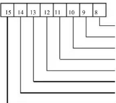 If a parameter needs to be displayed during the running, set the corresponding bit to 1, and set P7-0 4 to the hexadecimal equivalent of this binary number. If a parameter needs to be displayed during the running, set the corresponding bit to 1, and set P7-0 4 to the hexadecimal equivalent of this binary number. | |||
These two parameters are used to set the parameters that can be viewed when the AC drive is in the running state. You can view a maximum of 32 running state parameters that are displayed from the lowest bit of P7-03.
| P7-05 | LED display stop parameters | Factory default | 0 | ||
| Setting range | 0000~FFFF | 0000-FFFF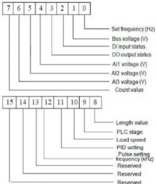 If a parameter needs to be displayed during the running, set the corresponding bit to 1, and set F7-05 to the hexadecimal equivalent of this binary number. If a parameter needs to be displayed during the running, set the corresponding bit to 1, and set F7-05 to the hexadecimal equivalent of this binary number. | |||
| P7-06 | Load speed display coefficient | Factory default | 1.0000 |
| Setting range | 0.0001~6.5000 | ||
When you need to display the load speed, this parameter, adjusting the correspondence between the output frequency and load speed. Correspondence between specific reference P7-12 description.
| P7-07 | Heat sink temperature of the inverter module | Factory default | 0 |
| Setting range | 0.0^ 100.0^ | ||
Display inverter module IGBT temperature.
Different models of inverter module IGBT overtemperature protection value is different.
| P7-08 | Rectifier heatsink temperature | Factory default | 0 |
| Setting range | 0.0^ 100.0^ | ||
Temperature display rectifier.
Different models of the rectifier overtemperature protection value is different.
| P7-09 | Total running time | Factory default | 0h |
| Setting range | 0h~65535h | ||
Displays the accumulated run time of the inverter. When running time reaches the set running time P8-17, the inverter multifunction digital output (12) outputs ON signal.
Parameter description
Specification of high-performance vector convertor
| P7-10 | Product No. | Factory default | ||
| Setting range | Inverter product number | |||
| P7-11 | Software version number | Factory default | ||
| Setting range | Control panel software version number. | |||
| P7-12 | Load speed display decimal digits | Factory default | 0 | |
| Setting range | 0 | 0 decimal places | ||
| 1 | 1 decimal places | |||
| 2 | 2 decimal places | |||
| 3 | 3 decimal places | |||
Load speed setting for the decimal display. The following example illustrates the calculation of load speed:
If the load speed display coefficient 2.000 P7-06, P7-12 load speed to 2 decimal places (two decimal places), when the inverter operating frequency 40.00Hz, the load speed: 40.00 × 2.000 = 80.00 (2 decimal places display)
If the drive is shut down, the load speed display setting frequency corresponding to the speed, that is, “to set the load speed.” To set the frequency 50.00Hz, for example, the stop state load speed: 50.00 × 2.000 = 100.00 (two decimal display)
| P7-13 | Cumulative power-up time | Factory default | 0h |
| Setting range | 0h~65535h | ||
Cumulative power-time display from the factory started the drive.
This time reaches the set power-up time (P8-17), the inverter multi-function digital output (24) outputs ON signal.
| P7-14 | The total power consumption | Factory default | - |
| Setting range | 0 to 65535 KWh | ||
So far show the total power consumption of the drive.
P8 Group--Auxiliary function
| P8-00 | Jog frequency | Factory default | 2.00Hz |
| Setting range | 0.00Hz ~ maximum frequency | ||
| P8-01 | Jog acceleration time | Factory default | 20.0s |
| Setting range | 0.00s~6500.0s | ||
| P8-02 | Jog Deceleration time | Factory default | 20.0s |
| Setting range | 0.00s~6500.0s | ||
When you define the drive jog a given frequency and the deceleration time.
Jog running, start fixed direct start-up mode (P6-00 = 0), stop mode is fixed to decelerate stop (P6-10 = 0).
| P8-03 | Acceleration time 2 | Factory default | 20.0s |
| Setting range | 0.0s~6500.0s | ||
| P8-04 | Deceleration time 2 | Factory default | 20.0s |
| Setting range | 0.0s~6500.0s | ||
| P8-05 | Acceleration time 3 | Factory default | 20.0s |
| Setting range | 0.0s~6500.0s | ||
| P8-06 | Deceleration time 3 | Factory default | 20.0s |
| Setting range | 0.0s~6500.0s | ||
| P8-07 | Acceleration time 4 | Factory default | 20.0s |
| Setting range | 0.0s~6500.0s | ||
| P8-08 | Deceleration time 4 | Factory default | 20.0s |
| Setting range | 0.0s~6500.0s | ||
This VFD provides 4 group of acceleration and deceleration time, respectively P0-17 / P0-18 and said 3 group of acceleration and deceleration time.
4 group define exactly deceleration time, refer to the P0-17 and P0-18 instructions. Through different combinations of multifunction digital input terminal DI, you can switch between 4 group of acceleration and deceleration time, please refer to the specific use function code P4-01 \~ P4-05 of instructions.
| P8-09 | Skip frequency 1 | Factory default | 0.00Hz |
| Setting range | 0.00Hz ~ maximum frequency | ||
| P8-10 | Skip frequency 2 | Factory default | 0.00Hz |
| Setting range | 0.00Hz ~ maximum frequency | ||
| P8-11 | Jump frequency range | Factory default | 0.00Hz |
| Setting range | 0.00Hz ~ maximum frequency | ||
When the jump frequency range within the set frequency, the actual running frequency will run at a frequency from the set frequency jump closer. By setting the frequency hopping allows the drive to avoid the mechanical resonance point of load. VFD can set two skip frequencies, when the two skip frequencies are set to 0, the jump frequency function is canceled. Principle jump frequency and the amplitude of frequency hopping schematic, refer to Figure 6-14.
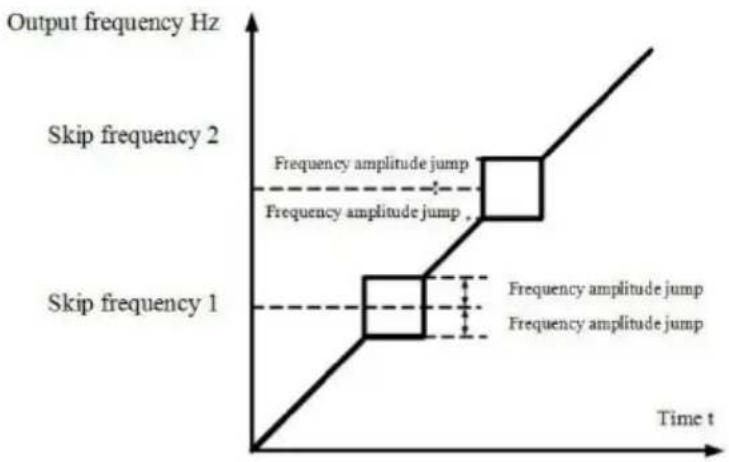
line
| Time t | Output frequency Hz | | ------ | ------------------- | | 0 | 0 | | 1 | 1 | | 2 | 2 |Figure 6-14 Skip frequency schematic
| P8-12 | Reversible dead time | Factory default | 0.0s |
| Setting range | 0.00s~3000.0s | ||
Set the inverter reversing the transition process, the output of 0Hz at the time of transition, shown in Figure 6-15:
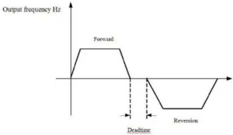
line
| Time Segment | Output Frequency (Hz) | | ------------ | --------------------- | | Forward | High | | Deadtime | Low | | Reversion | Low |Figure 6-15 Reversible schematic dead time
| P8-13 | Inversion of Control Enable | Factory default | 0 | |
| Setting range | 0 | Allow | ||
| 1 | Ban | |||
Set up the drive via the parameter is allowed to run in the inverted state, in the case of motor reversal is not allowed to set P8-13 = 1.
| P8-14 | Set frequency is lower than the lower limit frequency operation mode | Factory default | 0 | |
| Setting range | 0 | Operation in lower limit frequency | ||
| 1 | Shutdown | |||
| 2 | Running at zero speed | |||
When the set frequency is lower than minimum frequency, the operating status of the inverter can be selected using this parameter. VFD offers three operating modes to meet various application requirements.
| P8-15 | Droop control | Factory default | 0.00Hz |
| Setting range | 0.00Hz~10.00Hz | ||
This feature is typically used for load distribution of multiple motor drive with a load.
Droop control means that as the load increases, so that the inverter output frequency decreases, so more than one motor drive the same load, the load of the motor output frequency drops more, thereby reducing the load of the motor to achieve multiple motors load evenly.
This parameter refers to the inverter rated output load, the output value of the frequency drops.
| P8-16 | Set the accumulated power-on time | Factory default | 0h |
| Setting range | 0h~65000h | ||
When the accumulated power-on time (P7-13) P8-16 reach the set power-up time, the inverter multi-function digital output DO ON signal. The following examples illustrate the application:
Example: Combining virtual DIDO function, to achieve the set power-up time after reaching 100 hours, the inverter fault alarm output. Program:
Virtual DI1 terminal function set to user-defined fault 1: A1-00 = 44;
D11 virtual terminal active, is set to come from virtual DO1: A105 = 0000; virtual DO1 function, set the power-on time of arrival: A1-11 = 24; set the power accumulated 100 hours of arrival: P8-16 = 100.
When the cumulative power-up time of 100 hours, and the inverter fault output Err24.
| P8-17 | Set the accumulated run time | Factory default | 0h |
| Setting range | 0h~65000h | ||
It is used to set the running time of the inverter.
When the total running time (P7-09) reaches this setup running time, the inverter multi-function digital output DO ON signal.
| P8-18 | Start protection selection | Factory default | 0 | |
| Setting range | 0 | Does not protect | ||
| 1 | Protection | |||
This parameter is related to the security function of the inverter.
If this parameter is set to 1 if the time run on electric drive command is active (for example, a terminal run command before power is in a closed state), the inverter does not respond to the Run command, you must first run the command once removed, run the command again after the effective drive only response.
In addition, if the parameter is set to 1, if the inverter fault reset time run command, the inverter will not run in response to a command, you must first run the command to remove the running protection status.
Setting this parameter to 1 can be prevented in the knowledge, that occur at power or fault reset, the motor operates in response to commands and cause danger.
| P8-19 | Frequency detection value (FDT1) | Factory default | 50.00Hz |
| Setting range | 0.00Hz ~ maximum frequency | ||
| P8-20 | Frequency detection hysteresis value (FDT1) | Factory default | 5.0% |
| Setting range | 0.0% ~ 100.0% (FDT1 level) | ||
When the operating frequency higher than the frequency detection value, the inverter output DO multifunction output ON signal, and the frequency is lower than the detection value after a certain frequency, output ON DO signal is canceled.
Said parameter value is set for detecting the output frequency, output value and hysteresis action removed. Wherein P8-20 lag frequency percentage frequency detection value P8-19 respect. Figure 6-16 is a schematic diagram FDT functionality.
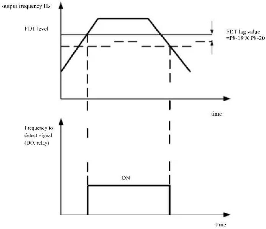
line
| Time | Output Frequency (Hz) | |------|------------------------| | 0 | Low | | Peak | High | | Lag | FDT lag value = P8-19 X P8-20 | | Low | Low | | High | FDT lag value = P8-19 X P8-20 |Figure 6-16 FDT level schematic
| P8-21 | Frequency arrival detection width | Factory default | 0.0% |
| Setting range | 0.0% to 100% (maximum frequency) | ||
Operating frequency of the inverter, and is in the target frequency range, the inverter output multifunction DO ON signal.
This parameter is used to set the frequency arrival detection range, the parameter is a percentage of the maximum frequency. Figure 6-17 is a schematic diagram of a frequency to reach.
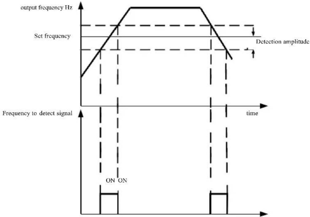
line
| Time | Output Frequency (Hz) | Detection Amplitude (dBm) | |------|------------------------|---------------------------| | 0 | Low | 0 | | 1 | Medium | High | | 2 | High | Medium | | 3 | High | Low | | 4 | High | Medium | | 5 | High | Low | | 6 | Low | 0 |Figure 6-17 Frequency arriving detection amplitude schematic
| P8-22 | Acceleration and deceleration process Jump frequency whether it is valid | Factory default | 0 |
| Setting range | 0: Invalid1: Valid | ||
The function code is used to set, during acceleration or deceleration, the jumping frequency is valid. Is set to be valid when running at a frequency hopping frequency range, the actual operating frequency will jump frequency setting to skip the border. Figure 6-18 acceleration and deceleration process schematic jump frequency is effective.
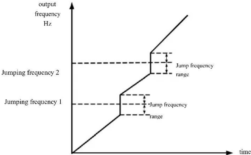
line
| Time | Output Frequency (Hz) | |------|------------------------| | 1 | Jump frequency 1 | | 2 | Jump frequency 2 |Figure 6-18 acceleration and deceleration process Jump frequency effective schematic
| P8-25 | Acceleration time Acceleration time 1 and 2 switching frequency points | Factory default 0.00Hz | |
| Setting range | 0.00Hz ~ maximum frequency | ||
| P8-26 | Deceleration time 2 and deceleration time 1 switching frequency point | Factory default | 0.00Hz |
| Setting range | 0.00Hz to maximum frequency | ||
This function is selected as the motor in the motor 1, and not switched by DI terminal when selecting acceleration and deceleration time is valid. For the inverter is running, but not according to the operating frequency range to choose different acceleration and deceleration times by DI terminals.
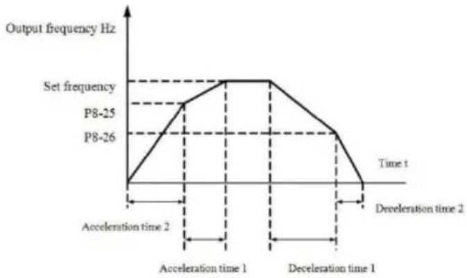
line
| Time Point | Output Frequency (Hz) | | ---------------------- | --------------------- | | Start of Acceleration | 0 | | Peak of Acceleration | P8-25 | | Peak of Deceleration | P8-26 | | End of Deceleration | 0 |Figure 6-19 acceleration and deceleration time switch schematic
Figure 6-19 is a schematic view of acceleration and deceleration time switching. During acceleration, if the operating frequency is less than P8-25 selects the acceleration time 2; if the operating frequency is greater than the acceleration time 1 Select P8-25.
During deceleration, if the operating frequency is greater than P8-26 Deceleration Time 1 is selected, if the operating frequency is less than the deceleration time 2 Select P8-26.
| P8-27 | Terminal jog priority | Factory default | 0 |
| Setting range | 0: Invalid 1: Valid | ||
This parameter is used to set whether the terminal jogging function has the highest priority.
When the terminal jogging priority effective, if the terminal point move command occurs during operation, the drive is switched to the terminal jogging running.
| P8-28 | Frequency detection value (FDT2) | Factory default | 50.00Hz |
| Setting range | 0.00Hz ~ maximum frequency | ||
| P8-29 | Frequency detection hysteresis value (FDT2) | Factory default | 5.0% |
| Setting range | 0.0% ~ 100.0% (FDT2 level) | ||
The frequency detection function FDT1 the same functions FDT1 refer to the instructions that function code P8-19, P8-20 description.
| P8-30 | Any reached frequency detection value 1 | Factory default | 50.00Hz |
| Setting range | 0.00Hz ~ maximum frequency | ||
| P8-31 | Any reached frequency detection range 1 | Factory default | 0.0% |
| Setting range | 0.0% to 100.0% (maximum frequency) | ||
| P8-30 | Any reached frequency detection value 2 | Factory default | 50.00Hz |
| Setting range | 0.00Hz ~ maximum frequency | ||
| P8-31 | Any reached frequency detection range 2 | Factory default | 0.0% |
| Setting range | 0.0% to 100.0% (maximum frequency) | ||
When the output frequency of the inverter, when arriving at any frequency detection value detected positive and negative amplitude range, multi-DO output ON signal.
VFD arrival frequency detection provides two sets of arbitrary parameters were set frequency value and frequency detection range. 6-20 schematic diagram for the function.
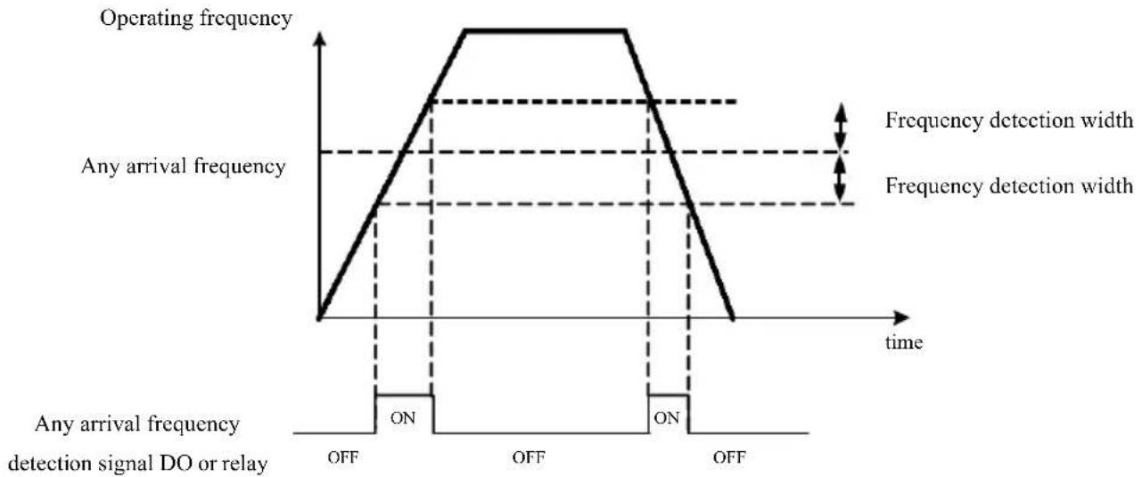
line
| Time | Operating Frequency | Frequency Detection Width | |------|---------------------|----------------------------| | OFF | 0 | ON | | OFF | 1.5 | ON | | OFF | 1.5 | ON |Figure 6-20 arbitrary frequency detection arrival schematic
| P8-34 | Zero-current detection level | Factory default | 5.0% |
| Setting range | 0.0%~300.0% (motor rated current) | ||
| P8-35 | Zero-current detection delay time | Factory default | 0.10s |
| Setting range | 0.00s~600.00s | ||
When the inverter output current is less than or equal to zero current detection level and lasts longer than the zero current detection delay time, the inverter output multifunction DO ON signal. Figure 6-21 zero current detection Fig.
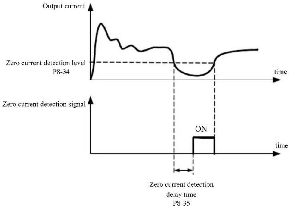
line
| Time Point | Output Current | Zero Detection Signal | | ---------- | -------------- | ---------------------- | | P8-34 | Peak | - | | P8-35 | Low | ON |Figure 6-21 Zero current detection schematic
| P8-36 | Output current limit value | Factory default | 200.0% |
| Setting range | 0.0 % (not detected)0.1%~300.0% (motor rated current) | ||
| P8-37 | Output current limit detection delay time | Factory default | 0.00s |
| Setting range | 0.00s~600.00s | ||
When the inverter output current is greater than or overrun detection point, and lasts longer than the software overcurrent detection delay time, the inverter output multifunction DO ON signal Figure 6-22 output current limit function schematic.
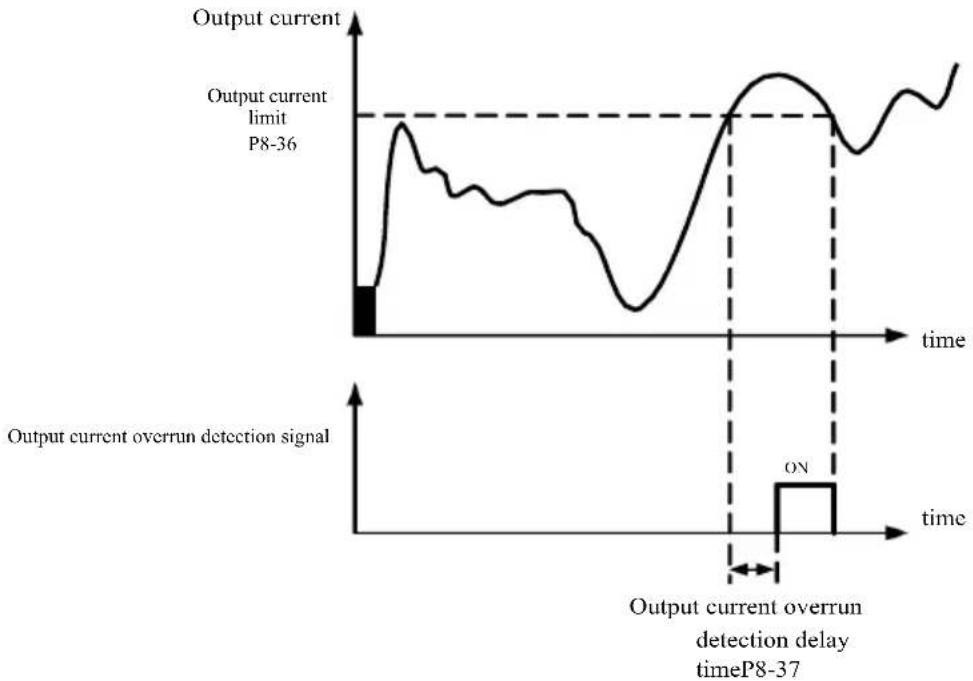
line
| Time Point | Output Current | Output Current Overrun Detection Signal | | ---------- | -------------- | ---------------------------------------- | | P8-36 | High | Not labeled | | P8-37 | Low | ON |Figure 6-22 Output current limit detection schematic
| P8-38 | Any arrival current 1 | Factory default | 100.0% |
| Setting range | 0.0%~300.0% (motor rated current) | ||
| P8-39 | Any arrival current width 1 | Factory default | 0.0% |
| Setting range | 0.0%~300.0% (motor rated current) | ||
| P8-40 | Any arrival current 2 | Factory default | 100.0% |
| Setting range | 0.0%~300.0% (motor rated current) | ||
| P8-41 | Any arrival current width 2 | Factory default | 0.0% |
| Setting range | 0.0%~300.0% (motor rated current) | ||
When the output current of the inverter, setting the current reach any positive or negative detection width, the inverter output multifunction DO ON signal.
VFD provides two sets of current and any arrival detection width parameter, a functional schematic diagram in Figure 6-23.
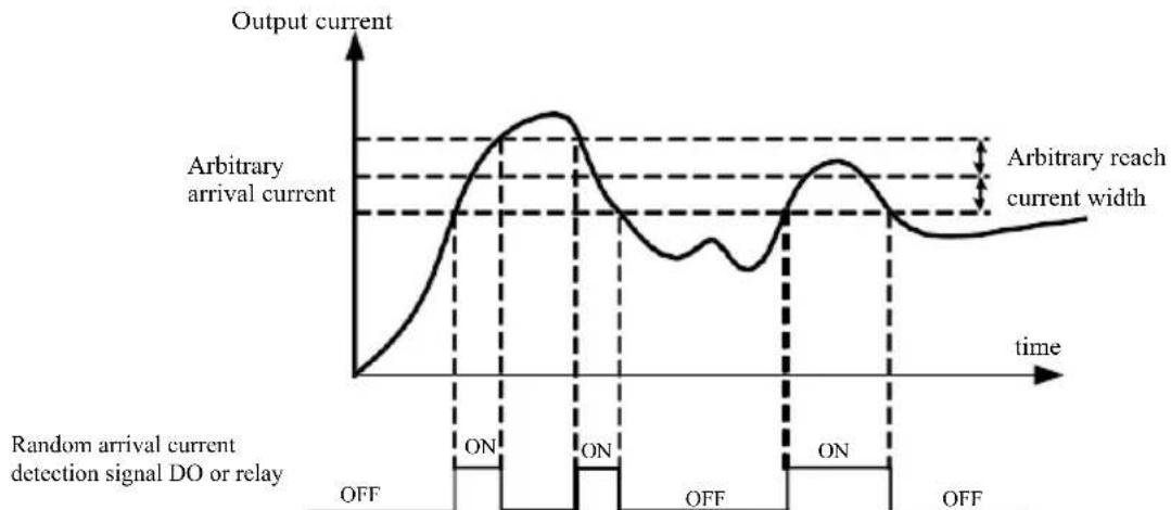
line
| Time | Output Current | |------|----------------| | OFF | 0 | | ON | ON | | ON | ON | | OFF | 0 | | ON | ON | | OFF | 0 |Figure 6-23 Schematic diagram of any arrival current detection
| P8-42 | Timing function selection | Factory default | 0 | |
| Setting range | 0 | Invalid | ||
| 1 | Valid | |||
| P8-43 | Timed Run time selection | Factory default | 0 | |
| Setting range | 0 | Setting P8-44 | ||
| 1 | AI1 | |||
| 2 | AI2 | |||
| 3 | AI3 | |||
| Analog Input Range 100% correspond to P8-44 | ||||
| P8-44 | Timed Run Time | Factory default | 0.0Min | |
| Setting range | 0.0Min~6500.0Min | |||
The set of parameters used to complete the drive timing running function.
When P8-42 timing function selection is valid, the inverter starts the beginning of time, after reaching set the timer run time, the inverter automatically shut down, while multi-function DO output ON signal.
When the drive each time you start, you start counting from 0, time remaining operating time by U0-20 view. Regular operation time set by P8-43, P8-44, the time in minutes.
| P8-45 | All input voltage protection lower limit values | Factory default | 3.10V |
| Setting range | 0.00V~P8-46 | ||
| P8-46 | All input voltage protection upper limit values | Factory default | 6.80V |
| Setting range | P8-45~10.00V | ||
When the value is greater than the analog input AI1 P8-46, P8-47 less than or AI1 input, the output of the inverter multifunction DO “AI1 input overrun” ON signal for indicating AI1 input voltage is within a set range.
| P8-47 | Module temperature reached | Factory default | 75°C |
| Setting range | 0.00V~P8-46 | ||
The inverter heat sink temperature reaches this temperature, the inverter output multifunction DO “module temperature reaches the” ON signal.
| P8-48 | Cooling fan control | Factory default | 0 |
| Setting range | 0: fan operates when running1: The fan has been running | ||
It is used to select the cooling fan operation mode selection 0. Inverter fan running in the running state, stop state if the heat sink temperature is higher than 40 degrees then the fan is running, stop state radiator fan is not lower than 40 degrees operation.
Select 1, the fan after power has been running.
| P8-49 | Wake frequency | Factory default | 0.00Hz |
| Setting range | Sleep frequency (P8-51) ~ maximum frequency (P0-10) | ||
| P8-50 | Wake-up delay time | Factory default | 0.0s |
| Setting range | 0.0s~6500.0s | ||
| P8-51 | Sleep frequency | Factory default | 0.00Hz |
| Setting range | 0.00Hz ~ wake-frequency (P8-49) | ||
| P8-52 | Sleep latency | Factory default | 0.0s |
| Setting range | 0.0s~6500.0s | ||
This group used to implement the water supply system in sleep and wake function.
The inverter is running, when the set frequency is less than or equal P8-51 Sleep frequency, P8-52 after the delay time, the drive goes to sleep, and automatically shut down. If the drive is in a dormant state, and the current run command, when the set frequency greater than or equal frequency wake P8-49, P8-50 after a time delay, the drive started.
In general, set the wake-sleep frequency greater than or equal frequency. Sleep and wake-up frequency setting frequency was 0.00Hz, then sleep and wake up function is invalid.
When hibernation is enabled, if the frequency source using PID, the PID sleep state whether operations by PA-28 affect the function code, in which case you must select the shutdown operation when PID (PA-28 = 1).
| P8-53 | The running time of arrival | Factory default | 0.0Min |
| Setting range | 0.0Min~6500.0Min | ||
When this started running time arrival this time, the inverter multi-function digital output DO “The running time arrival” ON signal.
P9 Group--Fault and Protection
| P9-00 | Motor overload protection selection | Factory default | 1 | |
| Setting range | 0 | Ban | ||
| 1 | Allow | |||
| P9-01 | Motor overload protection gain | Factory default | 1.00 | |
| Setting range | 0.20~w10.00 | |||
P9-00 = 0: No motor overload protection function may present a risk of damage to the motor overheating, the proposed increase thermal relay between the inverter and the motor;
P9-00 = 1: the frequency converter according to the motor overload inverse time curve to determine whether the motor is overloaded. Motor overload inverse time curve: 220% × (P9 - 01) × motor rated current for 1 minute, the alarm of motor overload fault; 150% × (P9 - 01) × rated motor current, the motor 60 minutes the alarm overload.
User according to the actual motor overload, set the correct value of P9-01, this parameter is set too easily lead to motor overheating and the risk of damage to the inverter not alarm!
| P9-02 | Motor overload warning coefficient | Factory default 80% |
| Setting range | 50%~100% |
This function is used before the motor overload fault protection, through DO to the control system a warning signal. The warning coefficient is used to determine, before the motor overload early warning extent. The higher the value the smaller the amount of advance warning.
When the inverter output current cumulative amount greater than overload inverse curves and P9-02 product, multifunction drive DO digital output “motor overload pre-alarm” ON signal.
| P9-03 | Overvoltage stall gain | Factory default | 0 |
| Setting range | 0 (no overvoltage stall)~100 | ||
| P9-04 | Overvoltage stall protection voltage | Factory default | 130% |
| Setting range | 120%~150% (threc-phase) | ||
During the deceleration, when the DC bus voltage exceeds the overvoltage stall protection voltage, the inverter stop deceleration is maintained at the current operating frequency, voltage drops until the bus continues to decelerate.
Overvoltage stall gain for adjusting during deceleration, the drive capacity in suppressing the pressure. The bigger the value, the stronger the ability to suppress the overvoltage. Without overvoltage occurs, the gain is set as small as possible.
For small inertia load, over-voltage stall gain should be small, otherwise the system dynamic response slow. For large inertia loads, this value should be large, otherwise the suppression ineffective, overvoltage fault may occur.
Overvoltage stall when the gain is set to 0, the cancellation of overvoltage stall function.
| P9-05 | Over current stall gain | Factory default | 20 |
| Setting range | 0 ~100 | ||
| P9-06 | Overcurrent stall protection current | Factory default | 150% |
| Setting range | 100% ~ 200% | ||
In the inverter deceleration process, when the output current exceeds the overcurrent stall protection current, the inverter stops deceleration process is maintained at the current operating frequency, output current drops and then continue to be deceleration.
Over-flow speed gain is used to adjust the acceleration and deceleration process, the drive capacity in suppressing the flow. The bigger the value, the stronger the capacity is. In the stream without happened next, the gain is set as small as possible.
For small inertia load, over-current stall gain should be small, otherwise the system dynamic response slow. For large inertia loads, this value should be large, otherwise the suppression ineffective, overcurrent fault may occur.
0 when the stall gain is set to cancel the stall function.
| P9-07 | Power-to-ground short circuit protection | Factory default | 1 | |
| Setting range | 0 Invalid | |||
| 1 Valid | ||||
Select the inverter at power, detecting whether the motor is shorted to ground.
If this function is active, the UVW side of the inverter after power-output voltage will be a period of time.
| P9-09 | Fault auto reset times | Factory default | 0 |
| Setting range | 0 ~ 20 | ||
When the inverter selects fault auto reset, used to set the number of auto reset. More than this number of times the drive remains a fault condition.
| P9-10 | During the auto-reset fault DO action selection | Factory default | 1 |
| Setting range | 0: no action1: Action | ||
If the drive is set up automatic fault reset function, then during automatic fault reset, fault DO whether action can be set by P9-10.
| P9-11 | Fault automatic reset interval | Factory default | 1.0s |
| Setting range | 0.1s ~ 100.0s | ||
Since the inverter fault alarm, automatic fault reset time to wait between.
| P9-12 | Input phase loss protection selection | Factory default | 1 |
| Setting range | 0: ban1: allow | ||
Select whether the input phase loss protection.
Inverter 18.5kW G-type machines and more power, have input phase protection, 18.5kW P-type machine less power. Regardless of P9-12 is set to 0 or 1 have no input phase loss protection.
| P9-13 | Output phase loss protection selection | Factory default | 1 |
| Setting range | 0: ban1: allow | ||
Choose whether to output phase loss protection.
| P9-14 | The first type of failure | 0~99 |
| P9-15 | The second type of failure | |
| P9-16 | The second (last) fault type |
Recording drive last three fault types, 0 is no fault. On possible causes and solutions for each fault code, please refer to Chapter 8 for instructions.
| P9-17 | The second fault frequency | Last frequency fault | |||||||||
| P9-18 | The second fault current | Last fault current | |||||||||
| P9-19 | The second bus voltage failure | Last bus voltage fault | |||||||||
| P9-20 | Input terminal status at fault second | Last fault state when the digital input terminals, the order is:BIT9 BIT8 BIT7 BIT6 BIT5 BIT4 BIT3 BIT2 BIT1 BIT0DI0 DI9 DI8 DI7 DI6 DI5 DI4 DI3 DI2 DI1When the input terminals of the corresponding two of N is set to 1, OFF or 0, the status of all DI converted to decimal display. | |||||||||
| P9-21 | The second fault output terminal | Last fault state when the digital input terminals, the order is:BIT4 BIT3 BIT2 BIT1 BIT0DO2 DO1 REL2 REL1 FMPWhen the input terminals of the corresponding two of N is set to 1, OFF or 0, the status of all DI converted to decimal display. | |||||||||
| P9-22 | The second fault drive status | Retention | |||||||||
| P9-23 | The second fault power-on time | The second power-up time of the last fault | |||||||||
| P9-24 | The second fault running time | The running time of the last fault | |||||||||
| P9-27 | The second fault frequency | The same with P9-17~P9-24 | |||||||||
| P9-28 | The second fault current | ||||||||||
| P9-29 | The second bus voltage failure | ||||||||||
| P9-30 | Input terminal status at fault second | ||||||||||
| P9-31 | The second fault output terminal | ||||||||||
| P9-32 | The second fault drive status | ||||||||||
| P9-33 | The second fault power-on time | ||||||||||
| P9-34 | The second fault running time | ||||||||||
| P9-37 | The first fault drive status | The same with P9-17~P9-24 | |||||||||
| P9-38 | The first fault power-on time | ||||||||||
| P9-39 | The first fault running time | ||||||||||
| P9-40 | The first fault frequency | ||||||||||
| P9-41 | The first fault current | ||||||||||
| P9-42 | The first bus voltage failure | ||||||||||
| P9-43 | Input terminal status at fault first | ||||||||||
| P9-44 | The first fault output terminal | ||||||||||
| P9-47 | Fault protection action selection 1 | Factory default | 00000 | |
| Setting range | Single digit | Motor overload (Err11) | ||
| 0 | Freewheel | |||
| 1 | Halt according to halt mode | |||
| 2 | Continue to run | |||
| Ten bit | Input phase (Err12) (same unit) | |||
| Hundred bit | Output Phase (Err13) (same unit) | |||
| Thousand bit | External fault (Err15) (same unit) | |||
| Ten thousand bit | Communication Abnormal (Err16) (same unit) | |||
| P9-48 | Fault protection action selection 2 | Factory default | 00000 | |
| Setting range | Single digit | Encoder failure (Err20) | ||
| 0 | Freewheel | |||
| 1 | Switch to VF, press the stop mode | |||
| 2 | Switch to VF, continues to run | |||
| Ten bit | Abnormal function code reader (Err21) | |||
| 0 | Freewheel | |||
| 1 | Halt according to halt mode | |||
| Hundred bit | Retention | |||
| Thousand bit | Motor overheating (Err 25) (same with P9-47 unit) | |||
| Ten thousand bit | Running time arrival (Err26) (same with P9-47 unit) | |||
| P9-49 | Fault protection action selection 3 | Factory default | 00000 | |
| Setting range | Single digit | User-defined fault 1 (Err27) (same with P9-47 unit) | ||
| Ten bit | User-defined fault 2 (Err28) (same with P9-47 unit) | |||
| Hundred bit | Power-on time is reached (Err29) (same with P9-47 unit) | |||
| Thousand bit | Carrying out (Err30) | |||
| 0 | Freewheel | |||
| 1 | Halt according to halt mode | |||
| 2 | Decelerated to 7% of the rated motor frequency continues to run, can not afford to load automatically returns to the set frequency operation | |||
| Ten thousand bit | Runtime PID feedback loss (Err31) (same with P9-47 unit) | |||
| P9-50 | Fault protection action selection 4 | Factory | 00000 | |
| Setting range | Single digit | Excessive speed deviation (Err42) (with P9-47 bits) | ||
| Ten bit | Super speed motor (Err43) (with P9-47 bits) | |||
| Hundred bit | The initial position error (Err51) (with P9-47 bits) | |||
| Thousand bit | the initial position error (Err52) (with P9-47 bits) | |||
| Ten thousand bit | Retention | |||
When you select "free parking", inverter displays Err **, and directly down.
When selecting the “stop in stopping mode”: The inverter displays A **, press the stop mode, the display Err ** after the shutdown.
When you select the “continue”: drive continues to operate and display A **, the operating frequency is set by the P9-54.
| P9-54 | Continue to run frequency selection | Factory default | 0 | |
| Setting range | 0 | In the current operating frequency operation | ||
| 1 | Operation in set frequency | |||
| 2 | Operation in upper limit frequency | |||
| 3 Operation in lower limit frequency | ||||
| 4 | Alternate abnormal frequency operation | |||
| P9-55 | Abnormal alternative frequencies | Factory default | 100.0% | |
| Setting range | 60.0%~100.0% | |||
When the inverter is running a fault, and the fault handling is set to continue, the drive display A **, and operates at a frequency determined to P9-54.
When you select an alternate abnormal frequency operation, the value set by P9-55 is a percentage of the maximum frequency.
| P9-56 | Motor temperature sensor type | Factory default | 0 | |
| Setting range | 0 | No Temperature Sensor | ||
| 1 | PT100 | |||
| 2 | PT1000 | |||
| P9-57 | Motor overheating protection Factory default | 110°C | ||
| Setting range | 0°C~200°C | |||
| F9-58 | Motor overheating prediction alert | Factory default | 90°C | |
| Setting range | 0°C~200°C | |||
Temperature signal motor temperature sensor needs to be connected to the multifunction input and output expansion card, which is optional. Analog expansion card input AI3, can be used as motor temperature sensor input, the motor temperature sensor signal then AI3, PGND terminal.
VFD AI3 analog inputs of PT100 and PT1000 supports two kinds of motor temperature sensor, the sensor must be set to the correct type of use. Motor temperature values are displayed in the U0-34.
When the motor temperature exceeds the motor overheating protection threshold P9-57, inverter fault alarm, fault protection action and processed according to the selected mode.
When the motor temperature exceeds the threshold P9-58 motor overheating forecast, the drive multifunction digital output DO Motor overtemperature pre-alarm ON signal.
| P9-59 | Instantaneous stop action selection | Factory default | 0 | |
| Setting range | 0 | Invalid | ||
| 1 | Slow down | |||
| 2 | Slowdown stop | |||
| P9-60 | Momentary power failure deceleration frequency switching point | Factory default | 0.0% | |
| Setting range | 0.0%~100.0% | |||
| P9-61 | Instantaneous power voltage recovery judgment time | Factory default | 0.50s | |
| Setting range | 0.00s~100.00s | |||
| P9-62 | Instantaneous stop non-stop action judgment voltage | Factory default | 80.0% | |
| Setting range | 60.0%~100.0% (standard bus voltage) | |||
This feature means that in an instant power failure or a sudden drop in voltage, the inverter by reducing the output speed, back to reduce the load energy compensation inverter DC bus voltage to maintain the drive continues to run.
If P9-59 = 1, the instantaneous power failure or a sudden drop in voltage, the inverter deceleration, when the bus voltage is restored, the drive accelerates to the set frequency normal operation. Analyzing the bus voltage returns to normal is based on the normal bus voltage P9-61 and lasts longer than the set time
If P9-59 = 2, the instantaneous power failure or a sudden drop in voltage, the inverter will decelerate to a stop
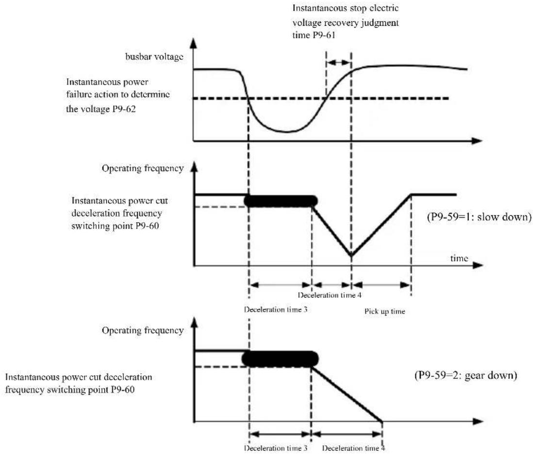
line
| Time Point | Busbar Voltage | Instantaneous Power Failure Action | Operating Frequency Change | | ---------- | -------------- | ----------------------------------- | -------------------------- | | P9-61 | High | Low | - | | P9-59=1 | Low | High | Slow down | | P9-59=2 | Low | Medium to High | Gear down |Figure 6-24 Schematic diagram of instantaneous power failure
| P9-63 | Load missing protection selection | Factory default | 0 | |
| Setting range | 0 | Invalid | ||
| 1 | Valid | |||
| P9-64 | Load missing detection level | Factory default | 10.0% | |
| Setting range | 0.0%~100.0% (motor rated current) | |||
| P9-65 | Load missing testing time | Factory default | 1.0s | |
| Setting range | 0.0s~60.0s | |||
If the load missing protection function is enabled, when the inverter output current is less than carrying out the detection level P9-64, and the duration is greater than the load loss detection time P9-65 when the output frequency is automatically reduced to 7% of the nominal frequency. During the off-load protection, if the load is restored, the drive automatically reverts to run at a set frequency.
| P9-67 | Over-speed detection value | Factory default | 15.0% | |
| Setting range 0.0% to 50.0% (maximum frequency) | ||||
| P9-68 | Over-speed detection time | Factory default | 2.0s | |
| Setting range | 0.0s~60.0s | |||
This function is only effective when the inverter running has speed sensor vector control.
When the drive detects the actual speed of the motor exceeds a set frequency, greater than the value exceeds the overspeed detection value P9-67, and the duration is greater than the over-speed detection time P9-68, the inverter fault alarm Err43, according to the fault and the protection mode deal with.
| P9-69 | Excessive speed deviation detection | Factory default | 20.0% | |
| Setting range 0.0% to 50.0% (maximum frequency) | ||||
| P9-70 | Excessive speed deviation detection | Factory default | 2.0s | |
| Setting range | 0.0s~60.0s | |||
This function is only effective when the inverter running has speed sensor vector control.
When the drive detects the actual speed of the motor and set frequency deviation, the deviation is greater than the speed deviation detection value P9-69, and the duration is greater than the speed deviation detection time P9-70, the inverter fault alarm Err42, and processed according to the operation mode fault protection.
When the speed deviation detection time is 0.0s, cancel the speed deviation fault detection.
PA Group--Process control PID function
PID control is a common method of process control by the controlled amount of the difference between the amount of the feedback signal and the target signal is proportional, integral, differential operation by adjusting the output frequency to form a closed-loop system, so that the amount charged in the stable target value.
Suitable for flow control, pressure control and temperature control and process control applications, PID control process block diagram of Figure 6-25.
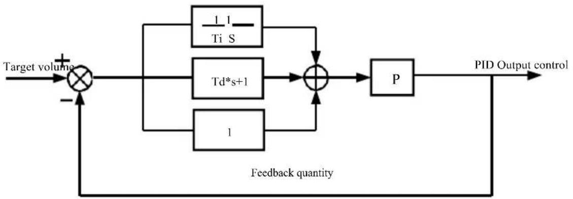
flowchart
graph LR
    A["Target volume"] --> B["×"]
    B --> C["Td*s+1"]
    C --> D["+"]
    D --> E["P"]
    E --> F["PID Output control"]
    F --> G["Feedback quantity"]
    G --> B
    H["1"] --> I["Ti S"]
    I --> D
    J["1"] --> K["Td*s+1"]
    K --> D
Figure 6-25 Principle block diagram of process PID
| PA-00 | PID given source | Factory default | 0 | |
| Setting range | 0 | PA-01 Set up | ||
| 1 | AI1 | |||
| 2 AI2 | ||||
| 3 AI3 | ||||
| 4 | Pulse (DI5) | |||
| 5 | Communication | |||
| 6 | Multi-step instructions | |||
| PA-01 | PID values given | Factory default | 50.0% | |
| Setting range | 0.0% ~ 100.0% | |||
This parameter is used to select target process PID given channel.
Set a target amount of process PID is a relative value, setting range 0.0% to 100.0%. The same amount is relatively PID feedback amount, PID is the role of these two relatively the same amount.
| PA-02 | PID feedback source | Factory default | 0 | |
| Setting range | 0 | AI1 | ||
| 1 | AI2 | |||
| 2 | AI3 | |||
| 3 | AI1 - AI2 | |||
| 4 | Pulse (DI5) | |||
| 5 | Communication | |||
| 6 | AI1+AI2 | |||
| 7 | MAX (|AI1|,|AI2|) | |||
| 8 | MIN (|AI1|,|AI2|) | |||
This parameter is used to select the process PID feedback signal path.
Process PID feedback amount for the relative value is set in the range of 0.0% to 100.0%.
| PA-03 | PID action direction | Factory default | 0 | |
| Setting range | 0 | Positive action | ||
| 1 | reaction | |||
R Positive effect: When the PID feedback signal is less than a given amount, the inverter output frequency rises. Such as winding tension control applications.
Reaction: When the PID feedback signal is less than a given amount, the output frequency decreases. As Unwinding tension control applications. The impact of the multi-function terminal function by PID action direction negated (function 35), the use of that need attention.
| PA-04 | PID given feedback range | Factory default | 1000 |
| Setting range | 0~65535 | ||
PID given feedback range is dimensionless units for a given display U0-15 PID and PID feedback display U0-16. Given relative value of feedback PID 100.0%, corresponding to a given feedback range PA-04. For example if the PA-40 is set to 2000, then when PID given 100.0%, PID given display U0-15 2000.
| PA-05 | Proportional gain Kp 1 | Factory default | 20.0 |
| Setting range | 0.0~100.0 | ||
| PA-06 | Integration time Ti 1 | Factory default | 2.00s |
| Setting range | 0.01s~10.00s | ||
| PA-07 | Differential time Td 1 | Factory default | 0.000s |
| Setting range | 0.00~10.000 | ||
Proportional gain Kp 1
Adjusting the intensity of the entire decision PID regulator, Kp1 the greater the greater the intensity. 100.0 This parameter indicates when the PID feedback value and a given amount of deviation of 100.0% when, PID controller to adjust the amplitude of the output frequency command is the maximum frequency.
Integration time Ti 1 Determine the intensity of PID regulator integral adjustment. The shorter the integration time adjustment intensity is. Integration time is when PID feedback quantity and given quantity of deviation of 100.0% of the time integral regulator continuous adjustment in the amount of the maximum frequency.
Differential time Td 1 PID regulator determines the rate of change of the deviation adjustment strength. Differential longer adjustment intensity is. Derivative time refers to the amount of change when the feedback 100.0% during that time, to adjust the amount of the differential regulator for the maximum frequency.
| PA-08 | PID reverse cut-off frequency | Factory default | 2.00Hz |
| Setting range 0.00 ~ maximum frequency | |||
In some cases, only when the PID output frequency is negative (ie, the drive reverse), PID is possible to control the amount of a given quantity and feedback to the same state, but the high frequency inversion is not allowed on some occasions the, PA-08 is used to determine the inversion frequency cap.
| PA-09 | PID deviation limit | Factory default | 0.01% |
| Setting range | 0.0%~100.0% | ||
When the PID deviation and feedback value is less than PA-09, PID stops adjustment operation. Thus, given the time and the feedback output frequency deviation of less stable and unchanging, closed-loop control on some occasions very effective.
| PA-10 | PID differential limiting | Factory default | 0.10% |
| Setting range | 0.00%~100.00% | ||
PID regulator, the differential effect is more sensitive and is likely to cause system oscillation, therefore, generally regarded PID derivative action is limited to a relatively small area, PA-10 is used to set the PID differential output range.
| PA-11 | PID given change time | Factory default | 0.00s |
| Setting range | 0.00s~650.00s | ||
PID given time changes, referring to PID setpoint changes from the 0.0% to 100.0% the time required.
When PID given change, PID setpoint changes linearly with time according to a given change, reduce the adverse effects of a given mutation on the system caused.
| PA-12 | PID feedback filter time | Factory default | 0.00s |
| Setting range | 0.00s~60.00s | ||
| PA-13 | PID output filter time | Factory default | 0.00s |
| Setting range | 0.00s~60.00s | ||
PA-12 for PID feedback filtering, the filter help to reduce the impact of the amount of feedback is disturbed, but the process will bring the response performance of the closed loop system.
PA-13 for PID output frequency filter, the filter will decrease the output frequency of the mutation, but it will also bring the performance of the process in response to the closed loop system.
| PA-15 | Proportional gain Kp 2 | Factory default | 20.0 | |
| Setting range | 0.0~100.0 | |||
| PA-16 | Integration time Ti 2 | Factory default | 2.00s | |
| Setting range | 0.01s~10.00s | |||
| PA-17 | Differential time Td 2 | Factory default | 0.000s | |
| Setting range | 0.00~10.000 | |||
| PA-18 | PID parameters switching | Factory default | 0 | |
| Setting range | 0 Not switch | |||
| 1 By DI terminal switch | ||||
| 2 | Automatic switching based on bias | |||
| PA-19 | PID parameter switching | Factory default | 20.0% | |
| Setting range | 0.0%~PA-20 | |||
| PA-20 | PID parameter switching | Factory default | 80.0% | |
| Setting range | PA-19~100.0% | |||
In some applications, a set of PID parameters can not meet the needs of the entire operation, and require different PID parameters under different circumstances.
This function code is used to switch two sets of PID parameters. Wherein the regulator parameter PA-15 is set up \~ PA-17, the parameter PA-05 \~ PA-07 is similar.
Two sets of PID parameters can be switched by multifunction digital terminals DI can also be automatically switched according to the deviation of PID.
When choosing a multifunction DI terminal switching, multi-function terminal function selection set to 43 (PID parameters switching terminal), select the parameter set 1 (PA-05 \~ PA-07) when the terminal is invalid, the terminal is valid parameter set selection 2 (PA-15 \~ PA-17).
Choose to automatically switch between the reference and feedback deviation is less than the absolute value of PID parameter switching deviation 1 PA-19 when, PID parameter selection parameter set 1. To a deviation between the reference and the PID feedback is greater than the absolute value of the deviation switch 2 PA-20 Shi, PID parameters select the parameter set 2. To a deviation between the reference and the feedback is switched when the deviation between 1 and switching deviation 2, PID parameters for the two sets of PID parameters of the linear interpolation value, as shown in Figure 6-26.
PI parameter
PID parameter1
PA-05、PA-06、PA-07
PID parameter2
PA-15、PA-16、PA-17
PA-19 PA-20
PID deviation
Figure 6-26 PID parameter switching
| PA-21 | Initial PID | Factory default | 0.0% |
| Setting range | 0.0%~100.0% | ||
| PA-22 | PID Initial Hold Time | Factory default | 0.00s |
| Setting range | 0.00s~650.00s |
When the inverter starts, PID PID output is fixed at the initial value PA-21, continuous PID initial value PA-22 after the holding time, PID loop adjustment operation began.
Figure 6-27 is the initial value of the PID function schematic.
output
frequency
PID
initial
value
PA-21
time
PID initial value hold time PA-22
Figure 6-27 is the initial value of the PID function schematic.
This function is used to limit the difference between the two beat PID output (2ms / beat) between the PID output in order to suppress the change too fast, so that the inverter operation to stabilize.
| PA-23 | Twice forward bias maximum | Factory default | 1.00% |
| Setting range | 0.00% ~ 100.00% | ||
| PA-24 | Twice forward bias maximum | Factory default | 1.00% |
| Setting range | 0.00% ~ 100.00% | ||
PA-23 and PA-24, respectively, and the maximum deviation of the output forward and reverse when the absolute value.
| PA-25 | PID integral property | Factory default | 00 | |
| Setting range | Single digit | Integral Separation | ||
| 0 Invalid | ||||
| 1 Valid | ||||
| Ten bit | Integral to whether to stop the output limit after | |||
| 0 Continued integration | ||||
| 1 Stop Points | ||||
Points separation:
If you set the integral separation effective, when multifunction digital integrator DI pause (function 22) is valid, PID integral PID integral stop operation, only this time PID proportional and derivative actions effective.
When selecting integral separation to be invalid, regardless of whether the DI digital multifunction effective, integral separation are not valid. Integral to whether to stop the output limit after: After PID operation output reaches a maximum or minimum, you can choose whether to stop the integral action. If you choose to stop the integration, at this time PID integral calculation is stopped, which may help reduce the PID overshoot.
| PA-26 | PID feedback loss detection value | Factory default | 0.0% |
| Setting range 0.0%: do not judge feedback loss | |||
| PA-27 | PID feedback loss detection time | Factory default | 1.0s |
| Setting range | 0.0s ~ 20.0s | ||
This function code is used to determine whether the loss of PID feedback.
When PID feedback is smaller than the feedback loss detection value of PA-26, and lasts longer than PID feedback loss detection time PA-27, the inverter alarm fault Err31, and troubleshooting process according to the selected mode.
| PA-28 | PID stoppage operation | Factory default | 0 | |
| Setting range | 0 | Do not stop operation | ||
| 1 Stoppage operation | ||||
PID is used to select the next stop status, PID whether to continue operations. General applications at standstill PID should stop operation.
PB Group--Swing Frequency, Fixed Length and Counting
Traverse function used in textile, chemical fiber industry, and the need to traverse, winding functions are required. Wobble function means that the inverter output frequency to set the frequency for the center swing up and down, the operating frequency of the track in the timeline.
As shown in Figure 6-28, which swings by the PB-00 and PB-01 set, when PB-01 is set to 0 swing 0, then wobble does not work.
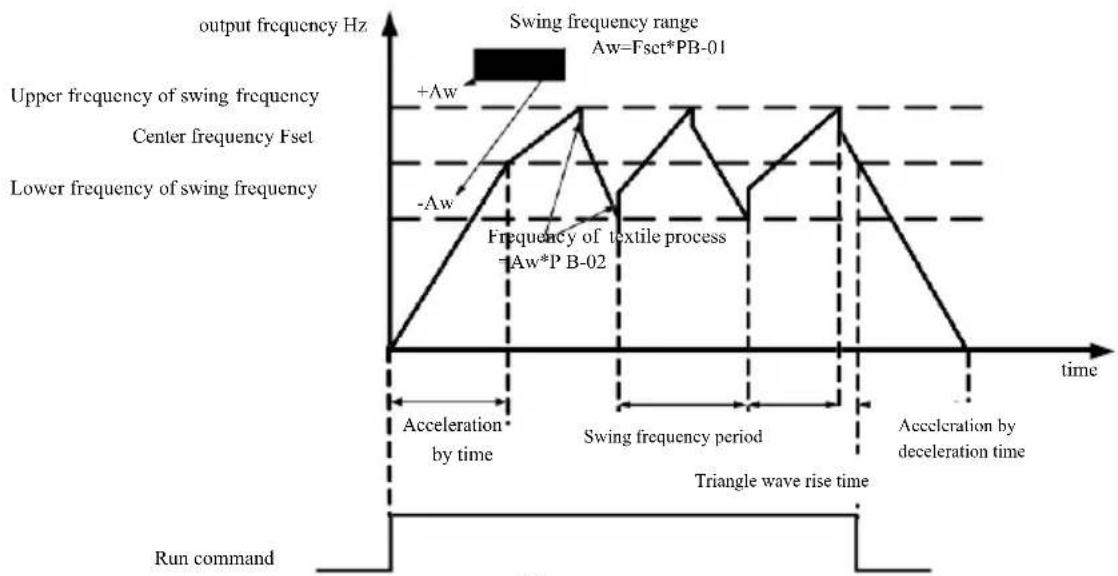
line
| Time Segment | Value | | ------------------------- | ----- | | Upper frequency of swing frequency | +Aw | | Center frequency Fset | -Aw | | Lower frequency of swing frequency | -Aw | | Frequency of textile process | -Aw*P B-02 | | Swing frequency period | -Aw*P B-02 | | Triangle wave rise time | -Aw*P B-02 | | Run command | -Aw |Figure 6-28 Working diagram of frequency swing
| PB-00 | Radiometric way swing | Factory default | 0 | |
| Setting range | 0 | corresponding to central frequency | ||
| 1 | Respect to the maximum frequency | |||
This parameter is determined by reference to the amount of swing.
0: relative to the center frequency (P0-07 frequency source), a variable-swing system. Swing with the center frequency (set frequency) change.
1: Relative maximum frequency (P0-10), the system is constant swing, swing fixed.
| PB-01 | Wobble amplitude | Factory default | 0.0% |
| Setting range | 0.0%~100.0% | ||
| PB-02 | Kick frequency amplitude | Factory default | 0.0% |
| Setting range | 0.0%~50.0% | ||
To determine the value of the swing and kick frequency value of this parameter.
When set to swing relative to the center frequency (PB-00 = 0), the swing AW = frequency source P0-07 × swing amplitude PB-01. When set to swing with respect to the maximum frequency (PB-00 = 1), the maximum frequency swing AW = P0-10 × swing amplitude PB-01.
Kick frequency amplitude of traverse run, the kick frequency relative to the frequency swing percentage, namely: kick frequency = swing AW × kick frequency amplitude PB-02. If the swing amplitude relative to the center frequency (PB-00 = 0), the kick frequency is a variable value. As selected swing relative to the maximum frequency (PB-00 = 1), the kick frequency is a fixed value.
Wobble operating frequency, maximum frequency and minimum frequency is bound by.
| PB-03 | Wobble cycle | Factory default | 10.0s |
| Setting range | 0.0s~3000.0s | ||
| PB-04 | Triangular wave rise time coefficient | Factory default | 50.0% |
| Setting range | 0.0%~100.0% | ||
Swing frequency cycle: a complete wobble cycle time value.
Triangular wave rise time coefficient PB-04, a triangular wave rising relatively wobble cycle PB-03 percentage of the time. Triangular wave rise time = Swing frequency cycle PB-03 × triangular wave rising time coefficient PB-04, in seconds. Triangular wave falling time = Swing frequency cycle PB-03 × (1-triangle wave rise time coefficient PB-04), in seconds.
| PB-05 | Set length | Factory default | 1000m |
| Setting range | 0m~65535m | ||
| PB-06 | Actual length | Factory default | 0m |
| Setting range | 0m~65535m | ||
| PB-07 | Number of pulses per meter | Factory default | 100.0 |
| Setting range | 0.1~6553.5 | ||
The above function codes for fixed-length control.
Length information you need to enter through the multifunction digital terminal acquisition, the number of sampling pulses terminals and the number of pulses per meter PB-07 phase in addition calculated to give actual length PB-06. When the actual length is greater than the set length PB-05, multi-function digital output DO “Length arrival” ON signal.
Fixed length control process, by multi-function terminal DI carried out the length of the reset operation (DI function selection 28). Please refer to P4-00 \~ P4-09.
Applications need to set the corresponding input terminal function set to “length count input” (function 27), at higher pulse frequency must be used DI5 port.
| PB-08 | Set count value | Factory default | 1000 |
| Setting range | 1~65535 | ||
| PB-09 | Designated counting value | Factory default | 1000 |
| Setting range | 1~65535 | ||
The count value required by multifunction digital input terminal acquisition. Applications need to set the corresponding input terminal function set to “counter input” (function 25), at higher pulse frequency must be used DI5 port.
When the count value reaches the set count value PB-08, multi-function digital output DO “reaching the set count” ON signal, then stop counting.
When the count reaches the designated counting value PB-09, the multi-function digital output DO “reaching the set count” ON signal, when the counting continues until “set count value” counter stopped.
Specified count number PB-09 should not be greater than the set counter value PB-08. Figure 6-29 is reaching the set count and the count value of the specified schematic reach capabilities.
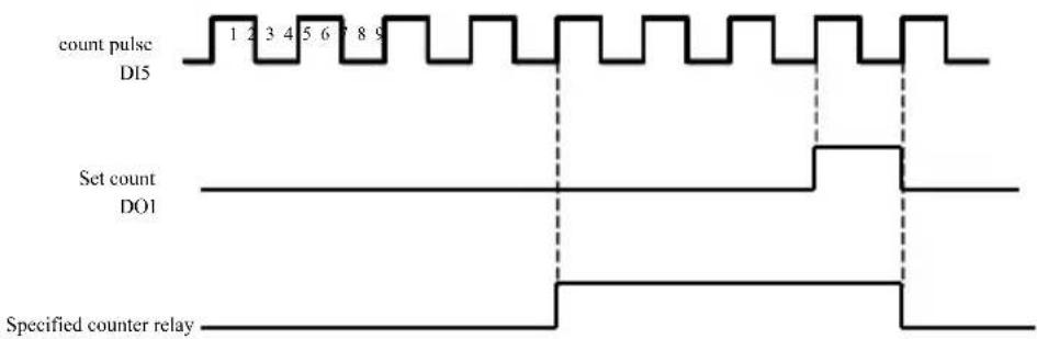
Figure 6-29 Set the number of values given and the specified value of the given diagram
PC Group--multi-section instructions and simple PLC function
Multi-stage instruction VFD than usual multispeed richer function, in addition to multi-speed function, but also can be used as VF isolated voltage source and a given source of process PID. To this end, the relative values of dimensionless multistage instruction.
Simple PLC function is different from the VFD user-programmable features, easy PLC can only be done on a simple combination of multi-step instructions to run. And user-programmed functions to be richer and more useful, please refer to the A7 group instructions.
| PC-00 | Multi-stage instruction 0 | Factory default | 0.0% |
| Setting range | -100.0%~100.0% | ||
| PC-01 | Multi-stage instruction 1 | Factory default | 0.0% |
| Setting range | -100.0%~100.0% | ||
| PC-02 | Multi-stage instruction 2 | Factory default | 0.0% |
| Setting range | -100.0%~100.0% | ||
| PC-03 | Multi-stage instruction 3 | Factory default | 0.0% |
| Setting range | -100.0%~100.0% | ||
| PC-04 | Multi-stage instruction 4 | Factory default | 0.0% |
| Setting range | -100.0%~100.0% | ||
| PC-05 | Multi-stage instruction 5 | Factory default | 0.0% |
| Setting range | -100.0%~100.0% | ||
| PC-06 | Multi-stage instruction 6 | Factory default | 0.0% |
| Setting range | -100.0%~100.0% | ||
| PC-07 | Multi-stage instruction 7 | Factory default | 0.0% |
| Setting range | -100.0%~100.0% | ||
| PC-08 | Multi-stage instruction 8 | Factory default | 0.0% |
| Setting range | -100.0%~100.0% | ||
| PC-09 | Multi-stage instruction 9 | Factory default | 0.0% |
| Setting range | -100.0%~100.0% | ||
| PC-10 | Multi-stage instruction 10 | Factory default | 0.0Hz |
| Setting range | -100.0%~100.0% | ||
| PC-11 | Multi-stage instruction 11 | Factory default | 0.0% |
| Setting range | -100.0%~100.0% | ||
| PC-12 | Multi-stage instruction 12 | Factory default | 0.0% |
| Setting range | -100.0%~100.0% | ||
| PC-13 | Multi-stage instruction 13 | Factory default | 0.0% |
| Setting range | -100.0%~100.0% | ||
| PC-14 | Multi-stage instruction 14 | Factory default | 0.0% |
| Setting range | -100.0%~100.0% | ||
| PC-15 | Multi-stage instruction 15 | Factory default | 0.0% |
| Setting range | -100.0%~100.0% | ||
Multi-step instructions can be used on three occasions: as the frequency source, as VF separate voltage source, as a process PID setting source.
Under three applications, multi-stage instruction dimensionless relative value, range -100.0% to 100.0%. When the frequency source as a percentage of its maximum relative frequency; VF as a separate voltage source, relative to the rated motor voltage percentage; and because PID originally given as a relative value, multi-source does not command as PID set dimension conversion.
Multi-step instruction required depending on the status of multi-function digital DI and switching options, please refer to the P4 group specific instructions.
| PC-16 | Simple PLC operation mode | Factory default | 0 | |
| Setting range | 0 | Stop at the end of single running | ||
| 1 | End of single running holding final value | |||
| 2 | Been circulating | |||
Simple PLC function has two roles: as the frequency source or as VF separate voltage source.
Figure 6-30 is a simplified schematic diagram of the PLC as the frequency source. When simple PLC as the frequency source, PC-00 \~ PC-15 determines the direction of the positive and negative, negative if it means running the drive in the opposite direction.

line
| Phase | Time (ms) | |---------|-----------| | PC-19 | 0 | | PC-21 | 0 | | PC-00 | 0 | | FC-01 | 0 | | PC-02 | 0 | | PC-14 | 0 | | PC-15 | 0 | | PC-18 | 0 | | PC-20 | 0 | | PC-23 | 0 | | DO or RELAY output | 0 | | 250m spulse | 0 |Figure6-30 Schematic diagram of simple PLC
As the frequency source, PLC operates in three ways, as a voltage source does not have VF separation of these three ways. among them:
0: stop at the end of single running
The drive to complete a single cycle stops automatically give a run command to start again.
1: One end of the run to keep the value of the final drive to complete a single cycle, automatically keep running frequency and direction of the last segment.
2: After the cycle has been completed a drive cycle, the next cycle starts automatically, until the stop command to stop.
| PC-17 | Simple PLC power down memory selection | Factory default | 00 | |
| Setting range | Single digit | Power-down memory selection | ||
| 0 | Memory is not down | |||
| 1 | Power off memory | |||
| Ten bit | Stop memory selection | |||
| 0 | Memory does not stop | |||
| 1 | Stop memory | |||
PLC down memory refers to memory before running down phase and frequency PLC running, the next phase will continue to run memory at power-up. Choose not to remember, then every power restart PLC process.
PLC shutdown memory is recorded once before shutdown phase and running frequency PLC running, the next phase will continue to run the memory at runtime. Choose not to remember, every time you restart the PLC process starts.
| PC-18 | Simple PLC running time of segment 0 | Factory default | 0.0s (h) |
| Setting range | 0.0s (h) ~6553.5s (h) | ||
| PC-19 | Simple PLC deceleration time of segment 0 | Factory default | 0 |
| Setting range | 0~3 | ||
| PC-20 | Simple PLC running time of segment 1 | Factory default | 0.0s (h) |
| Setting range | 0.0s (h) ~6553.5s (h) | ||
| PC-21 | Simple PLC deceleration time of segment 1 | Factory default | 0 |
| Setting range | 0~3 | ||
| PC-22 | Simple PLC running time of segment 2 | Factory default | 0.0s (h) |
| Setting range | 0.0s (h) ~6553.5s (h) | ||
| PC-23 | Simple PLC deceleration time of segment 2 | Factory default | 0 |
| Setting range | 0~3 | ||
| PC-24 | Simple PLC running time of segment 3 | Factory default | 0.0s (h) |
| Setting range | 0.0s (h) ~6553.5s (h) | ||
| PC-25 | Simple PLC deceleration time of segment 3 | Factory default | 0 |
| Setting range | 0~3 | ||
| PC-26 | Simple PLC running time of segment 4 | Factory default | 0.0s (h) |
| Setting range | 0.0s (h) ~6553.5s (h) | ||
| PC-27 | Simple PLC deceleration time of segment 4 | Factory default | 0 |
| Setting range | 0~3 | ||
| PC-28 | Simple PLC running time of segment 5 | Factory default | 0.0s (h) |
| Setting range | 0.0s (h) ~6553.5s (h) | ||
| PC-29 | Simple PLC deceleration time of segment 5 | Factory default | 0 |
| Setting range | 0~3 | ||
| PC-30 | Simple PLC running time of segment 6 | Factory default | 0.0s (h) |
| Setting range | 0.0s (h) ~6553.5s (h) | ||
| PC-31 | Simple PLC deceleration time of segment 6 | Factory default | 0 |
| Setting range | 0~3 | ||
| PC-32 | Simple PLC running time of segment 7 | Factory default | 0.0s (h) |
| Setting range | 0.0s (h) ~6553.5s (h) | ||
| PC-33 | Simple PLC deceleration time of segment 7 | Factory default | 0 |
| Setting range | 0~3 | ||
| PC-34 | Simple PLC running time of segment 8 | Factory default | 0.0s (h) |
| Setting range | 0.0s (h) ~6553.5s (h) | ||
| PC-35 | Simple PLC deceleration time of segment 8 | Factory default | 0 |
| Setting range | 0~3 | ||
| PC-36 | Simple PLC running time of segment 9 | Factory default | 0.0s (h) |
| Setting range | 0.0s (h) ~6553.5s (h) | ||
| PC-37 | Simple PLC deceleration time of segment 9 | Factory default | 0 |
| Setting range | 0~3 | ||
| PC-38 | Simple PLC running time of segment 10 | Factory default | 0.0s (h) |
| Setting range | 0.0s (h) ~6553.5s (h) | ||
| PC-39 | Simple PLC deceleration time of segment 10 | Factory default | 0 |
| Setting range | 0~3 | ||
| PC-40 | Simple PLC running time of segment 11 | Factory default | 0.0s (h) |
| Setting range | 0.0s (h) ~6553.5s (h) | ||
| PC-41 | Simple PLC deceleration time of segment 11 | Factory default | 0 |
| Setting range | 0~3 | ||
| PC-42 | Simple PLC running time of segment 12 | Factory default | 0.0s (h) |
| Setting range | 0.0s (h) ~6553.5s (h) | ||
| PC-43 | Simple PLC deceleration time of segment 12 | Factory default | 0 |
| Setting range | 0~3 | ||
| PC-44 | Simple PLC running time of segment 13 | Factory default | 0.0s (h) |
| Setting range | 0.0s (h) ~6553.5s (h) | ||
| PC-45 | Simple PLC deceleration time of segment 13 | Factory default | 0 |
| Setting range | 0~3 | ||
| PC-46 | Simple PLC running time of segment 14 | Factory default | 0.0s (h) |
| Setting range | 0.0s (h) ~6553.5s (h) | ||
| PC-47 | Simple PLC deceleration time of segment 14 | Factory default | 0 | |
| Setting range | 0~3 | |||
| PC-48 | Simple PLC running time of segment 15 | Factory default | 0.0s (h) | |
| Setting range | 0.0s (h) ~6553.5s (h) | |||
| PC-49 | Simple PLC deceleration time of segment 15 | Factory default | 0 | |
| Setting range | 0~3 | |||
| PC-50 | Simple PLC run time unit | Factory default | 0 | |
| Setting range | 0 | S (s) | ||
| 1 | h (h) | |||
| PC-5 | Multi-segment instruction 0 given mode | Factory default | 0 | |
| Setting range | 0 | Function code FC-00 given | ||
| 1 | AI1 | |||
| 2 | AI2 | |||
| 3 | AI3 | |||
| 4 | Pulse | |||
| 5 | PID | |||
| 6 | Preset frequency (P0-08) given, UPTOWN editable | |||
This parameter determines the multi-0 instruction given channel.
Multi-step instructions 0 PC-00 can be selected in addition, there are many other options to facilitate between multiple short instructions given with the other mode switching. When the multi-frequency source or instruction as simple as a PLC frequency source, can easily switch between the two to achieve frequency source.
PD Group--Communication parameters
Refer to VFD protocol
PE Group--Custom function code
| PE-00 | User Function Code 0 | Factory default | P0.00 | |
| Setting range | P0.00~PP.xx, A0.00~Ax.xx, U0.xx | |||
| PE-01 | User Function Code 1 | Factory default | P0.02 | |
| Setting range | P0.00~PP.xx, A0.00~Ax.xx, U0.xx | |||
| PE-02 | User Function Code 2 | Factory default | P0.03 | |
| Setting range | P0.00~PP.xx, A0.00~Ax.xx, U0.xx | |||
| PE-03 | User Function Code 3 | Factory default | P0.07 | |
| Setting range | P0.00~PP.xx, A0.00~Ax.xx, U0.xx | |||
| PE-04 | User Function Code 4 | Factory default | P0.08 | |
| Setting range | P0.00~PP.xx, A0.00~Ax.xx, U0.xx | |||
| PE-05 | User Function Code 5 | Factory default | P0.17 | |
| Setting range | P0.00~PP.xx, A0.00~Ax.xx, U0.xx | |||
| PE-06 | User Function Code 6 | Factory default | P0.18 | |
| Setting range | P0.00~PP.xx, A0.00~Ax.xx, U0.xx | |||
| PE-07 | User Function Code 7 | Factory default | P3.00 | |
| Setting range | P0.00~PP.xx, A0.00~Ax.xx, U0.xx | |||
| PE-08 | User Function Code 8 | Factory default | P3.01 | |
| Setting range | P0.00~PP.xx, A0.00~Ax.xx, U0.xx | |||
| PE-09 | User Function Code 9 | Factory default | P4.00 | |
| Setting range | P0.00~PP.xx, A0.00~Ax.xx, U0.xx | |||
| PE-10 | User Function Code 10 | Factory default | P4.01 | |
| Setting range | P0.00~PP.xx, A0.00~Ax.xx, U0.xx | |||
| PE-11 | User Function Code 11 | Factory default | P4.02 | |
| Setting range | P0.00~PP.xx, A0.00~Ax.xx, U0.xx | |||
| PE-12 | User Function Code 12 | Factory default | P5.04 | |
| Setting range | P0.00~PP.xx, A0.00~Ax.xx, U0.xx | |||
| PE-13 | User Function Code 13 | Factory default | P5.07 | |
| Setting range | P0.00~PP.xx, A0.00~Ax.xx, U0.xx | |||
| PE-14 | User Function Code 14 | Factory default | P6.00 | |
| Setting range | P0.00~PP.xx, A0.00~Ax.xx, U0.xx | |||
| PE-15 | User Function Code 15 | Factory default | P6.10 | |
| Setting range | P0.00~PP.xx, A0.00~Ax.xx, U0.xx | |||
| PE-16 | User Function Code 16 | Factory default | P0.00 | |
| Setting range | P0.00~PP.xx, A0.00~Ax.xx, U0.xx | |||
| PE-17 | User Function Code 17 | Factory default | P0.00 | |
| Setting range | P0.00~PP.xx, A0.00~Ax.xx, U0.xx | |||
| PE-18 | User Function Code 18 | Factory default | P0.00 | |
| Setting range | P0.00~PP.xx, A0.00~Ax.xx, U0.xx | |||
| PE-19 | User Function Code 19 | Factory default | P0.00 | |
| Setting range | P0.00~PP.xx, A0.00~Ax.xx, U0.xx | |||
| PE-20 | User Function Code 20 | Factory default | P0.00 | |
| Setting range | P0.00~PP.xx, A0.00~Ax.xx, U0.xx | |||
| PE-21 | User Function Code 21 | Factory default | P0.00 | |
| Setting range | P0.00~PP.xx, A0.00~Ax.xx, U0.xx | |||
| PE-22 | User Function Code 22 | Factory default | P0.00 | |
| Setting range | P0.00~PP.xx, A0.00~Ax.xx, U0.xx | |||
| PE-23 | User Function Code 23 | Factory default | P0.00 | |
| Setting range | P0.00~PP.xx, A0.00~Ax.xx, U0.xx | |||
| PE-24 | User Function Code 24 | Factory default | P0.00 | |
| Setting range | P0.00~PP.xx, A0.00~Ax.xx, U0.xx | |||
| PE-25 | User Function Code 25 | Factory default | P0.00 | |
| Setting range | P0.00~PP.xx, A0.00~Ax.xx, U0.xx | |||
| PE-26 | User Function Code 26 | Factory default | P0.00 | |
| Setting range | P0.00~PP.xx, A0.00~Ax.xx, U0.xx | |||
| PE-27 | User Function Code 27 | Factory default | P0.00 | |
| Setting range | P0.00~PP.xx, A0.00~Ax.xx, U0.xx | |||
| PE-28 | User Function Code 28 | Factory default | P0.00 | |
| Setting range | P0.00~PP.xx, A0.00~Ax.xx, U0.xx | |||
| PE-29 | User Function Code 29 | Factory default | P0.00 | |
| Setting range | P0.00~PP.xx, A0.00~Ax.xx, U0.xx | |||
This function code is customized parameter set.
Users can all VFD function code, select the desired parameter aggregated into PE group, as a user customized parameters for easy viewing and changing operations.
PE group provides up to 30 custom parameter, PE group parameter display is P0.00, it means that the user function code is empty. When entering custom parameters mode, display the function code PE-00 \~ PE-31 is defined by the order consistent with the PE group function code, skip to P0-00
PP Group--User password
| PP-00 | User Password | Factory default | 0 |
| Setting range | 0~65535 | ||
PP-00 to set an arbitrary non-zero number, the password protection function. The next time you enter the menu, you must enter the correct password, or can not view and modify function parameters, please remember the password set by the user.
PP-00 is set to 00000, then clear the user password set, the password protection function is invalid.
| PP-01 | Parameter Initialization | Factory default | 0 | |
| Setting range | 0 | No operation | ||
| 1 | Restore factory settings, not including the motor parameters | |||
| 2 | Clear History Information | |||
| 4 | Current backup user parameters | |||
| 501 | Recover user backup parameters | |||
- Restore factory settings, excluding motor parameters
PP-01 is set to 1, most inverter function parameters are restored to the factory default parameters, but motor parameters, frequency command decimal point (P0-22), fault recording information, total running time (P7-09), the cumulative power time (P7-13), the total power consumption (P7-14) is not restored.
- Clear History Information
Clear fault record information drive, total running time (P7-09), the cumulative power-up time (P7-13), the total power consumption (P7-14).
- The current parameter backup user
The current backup parameters set by the user. The current value of all settings function parameters back down. To facilitate customers in the parameter adjustment disorder after recovery.
501, restore the user parameters previously backed up user parameters backup recovery, the recovery by setting PP-01 for the four backup parameter.
| PP-02 | Function parameter display properties | Factory default | 11 | |
| Setting range | Single digit | U group display selection | ||
| 0 | Do not show | |||
| 1 | Show | |||
| Ten bit A group display selection | ||||
| 0 | Do not show | |||
| 1 | Show | |||
| PP-02 | Function parameter display properties | Factory default | 11 | |
| Setting range | Single digit | U group display selection | ||
| 0 | Do not show | |||
| 1 | Show | |||
| Ten bit A group display selection | ||||
| 0 | Do not show | |||
| 1 | Show | |||
Set up parameter display mode is mainly based on the actual user needs to view a different arrangement in the form of function parameters, provides three parameters display,
| Name | Description |
| Function parameters mode | Sequential display drive parameters, respectively, P0 ~ PF, A0 ~ AF, U0 ~ UF parameter group |
| Customized parametrical mode by users | Individual function parameters customized display (up to 32 customized), FE user group to determine the function of the parameters to be displayed |
| Parameter changing mode by users | Inconsistent with the factory parameter function parameters |
When the character mode display selection parameter (PP-03) when there is a show, this time can be switched to different parameters by QSM key display mode, the default is the only function parameter display.
| Parameter display mode | show |
| Function parameters mode | -hASF |
| Customized parametrical mode by users | -USER |
| Parameter changing mode by users | --F-- |
Each parameter display mode displays coded as:
VFD offers two personalized parameter display mode: The user customized parameters, the user change the parameter mode. Customized parameter sets for the user to set the parameters of PE group, you can select the maximum 32 parameters, which are aggregated together, customers can easily debug.
User customized parameters manner, before custom function code to add a default symbol u example: P1-00, in the custom parameter mode, the display for the user to change parameters for the uP1-00 way for users and manufacturers have to change in order to factory setting different parameters. User parameter set change in favor of the customer to view a summary of the parameters change, facilitate on-site to find the problem.
The user change the parameter mode, before the custom function code to add a default symbol c
For example: P1-00, change parameters in the user mode, the display is as cP1-00
| Function code to modify the properties | Factory default | 0 | ||
| PP-04 | Setting range | 0 | Can be modified | |
| 1 | Unmodifiable | |||
Whether the user function code parameter setting can be modified to prevent the risk of function parameters are mistakenly altered.
The function code is set to 0, all the function codes can be modified; while set to 1, all the function codes are only view can not be modified.
A0 Group --Torque control group and define parameters
| Speed / torque control mode selection | Factory default | 0 | ||
| A0-00 | Setting range | 0 | Speed Control | |
| 1 | Torque Control | |||
For selecting inverter control mode: Speed control or torque control.
DI VFD multifunction digital terminals, and has two functions associated with torque control: Torque control disabled (function 29), speed control / torque control switching (function 46). These two terminals keep A0-00 in conjunction to achieve switching speed and torque control.
When the speed control / torque control switch terminal is invalid, the control mode is determined by the A0-00, if speed control / torque control switch is active, the control mode is equivalent to the value of A0-00 negated.
In any case, when the torque control prohibition terminal is valid, inverter fixed speed control.
| Torque in torque control mode setting source selection | Factory default | 0 | |
| 0 | Number setting (A0-03) | ||
| 1 | AI1 | ||
| 2 | AI2 | ||
| A0-01 | Setting range | 3 | AI3 |
| 4 | Pulse | ||
| 5 | Communication given | ||
| 6 | MIN (AI1, AI2) | ||
| 7 | MAX (AI1, AI2) | ||
| A0-03 | Torque number setting in torque control mode | Factory default | 0 |
| Setting range | -200.0%~200.0% | ||
A0-01 torque setting is used to select the source, a total of 8 torque setting mode.
Torque setting using a relative value, corresponding to 100.0% inverter rated torque. Setting range -200.0% to 200.0%, indicating that the inverter maximum torque is 2 times the rated drive torque.
When the torque setting by way of 1 to 7, communications, analog input, pulse input of 100% corresponds to A0-03.
| A0-05 | Torque control positive maximum | Factory default | 50.00Hz |
| Setting range | 0.00Hz ~ maximum frequency (P0-10) | ||
| A0-06 | Torque control negative maximum | Factory default | 50.00Hz |
| Setting range | 0.00Hz ~ maximum frequency (P0-10) | ||
It is used to set the torque control mode, the drive forward or reverse maximum operating frequency.
When the drive torque control, if the load torque is less than the output torque of the motor, the motor speed will continue to rise, in order to prevent the mechanical system appears coaster accidents, it must be limited to the maximum torque of the motor speed control.
| A0-07 | Torque control acceleration time | Factory default | 0.00s | |
| Setting range | 0.00s~65000s | |||
| A0-08 | Torque control deceleration time | Factory default | 0.00s | |
| Setting range | 0.00s~65000s | |||
Torque control mode, the motor output torque and load torque difference determines the speed and rate of change of the motor load, so it is possible to quickly change the motor speed, causing noise or excessive mechanical stress and other issues. By setting the torque control acceleration and deceleration time, the motor speed can be so gradual change.
However, the need for rapid response in case of torque, set the torque control acceleration and deceleration time is 0.00s. For example: Two hard-wired motor drag the same load, to ensure that the load is evenly distributed, set up a drive for the host, using the speed control mode, the drive from another machine and using the actual output torque control switch, host moments torque command as a slave, this time the torque required to follow the host machine's fast, slave torque control acceleration and deceleration time is 0.00s.
A2 Group--2 ^nd motor
VFD can be switched between two motor, two motors can be set to the motor nameplate, respectively, can be the motor parameter tuning, respectively, can be selected VF control or vector control, you can set the encoder parameters, respectively, may be provided with VF control alone or vector control performance related parameters.
A2 group function code corresponds to the motor 2.
At the same time, all the parameters A2 group, the definition and use of its contents are consistent with the parameters of the 1^st motor, not repeated here, the user can refer to the first motor-related parameter description.
| A2-00 | Motor type selection | Factory default | 0 | |
| Setting range | 0 | General induction motor | ||
| 1 | Variable frequency induction motor | |||
| A2-01 | Rated power | Factory default | Model determination | |
| Setting range | 0.1kW~1000.0kW | |||
| A2-02 | rated voltage | Factory default | Model determination | |
| Setting range | 1V~400V | |||
| A2-03 | Rated current | Factory default | Model determination | |
| Setting range | 0.01A~655.35A(frequency converter power <=55kW) 0.1A~6553.5A(frequency converter power >55kW) | |||
| A2-04 | rated frequency | Factory default | Model determination | |
| Setting range | 0.01Hz~Maximum frequency | |||
| A2-05 | rated speed | Factory default | Model determination | |
| Setting range | 1rpm~65535rpm | |||
| A2-06 | Induction motor stator resistance | Factory default | Model determination | |
| Setting range | 0.001Ω~65.535Ω(frequency converter power <=55kW)0.0001Ω~6.5535Ω(frequency converter power >55kW) | |||
| A2-07 | Rotor resistance of induction motor | Factory default | Model determination | |
| Setting range | 0.001Ω~65.535Ω(frequency converter power <=55kW)0.0001Ω~6.5535Ω(frequency converter power >55kW) | |||
| A2-08 | The leakage inductance of asynchronous motor | Factory default | Model determination | |
| Setting range | 0.01mH~655.35mH(frequency converter power <=55kW)0.001mH~65.535mH(frequency converter power >55kW) | |||
| A2-09 | Induction motor mutual inductance | Factory default | Model determination | |
| Setting range | 0.1mH~6553.5mH(frequency converter power <=55kW) 0.01mH~655.35mH(frequency converter power >55kW) | |||
| A2-10 | No-load current of induction motor | Factory default | Model determination | |
| Setting range | 0.01A~A2-03(frequency converter power <=55kW)0.1A~A2-03(frequency converter power >55kW) | |||
| A2-27 | Encoder line number | Factory default | 1024 | |
| Setting range | 1~65535 | |||
| A2-28 | Speed fbk sel | Factory default | 0 | |
| Setting range | 0 | ABZ incremental encoder | ||
| Retention | ||||
| 1 | Rotating transformer | |||
| A2-29 | Speed feedback PG selection | Factory default | 0 | |
| Setting range | 0 | Local PG | ||
| 1 | Extension PG | |||
| 2 | PULSE pulse input (DI5) | |||
| A2-30 | ABZ incremental encoder AB sequence | Factory default | 0 | |
| Setting range | 0 | forward direction | ||
| 1 | reverse | |||
| A2-34 | Pole pairs of rotating transformer | Factory default | 1 | |
| Setting range | 1~65535 | |||
| A2-36 | Speed feedback PG disconnection detection time | Factory default | 0.0s | |
| Setting range | 0.0: failure to actuate0.1s~10.0s | |||
| A2-37 | Tuning selection | Factory default | 0 | |
| Setting range | 0 | No operation | ||
| 1 | Asynchronous machine static tuning | |||
| 2 | Full tuning of asynchronous machines | |||
| A2-38 | Speed loop proportional gain 1 | Factory default | 30 | |
| Setting range | 1~100 | |||
| A2-39 | Speed loop integral time 1 | Factory default | 0.50s | |
| Setting range | 0.01s~10.00s | |||
| A2-40 | Switching frequency 1 | Factory default | 5.00Hz | |
| Setting range | 0.00~A2-43 | |||
| A2-41 | Speed loop proportional gain 2 | Factory default | 15 | |
| Setting range | 0~100 | |||
| A2-42 | Speed loop integral time 2 | Factory default | 1.00s | |
| Setting range | 0.01s~10.00s | |||
| A2-43 | Switching frequency 2 | Factory default | 10.00Hz | |
| Setting range | A2-40~Maximum output frequency | |||
| A2-44 | Vector control transfer gain | Factory default | 100% | |
| Setting range | 50%~200% | |||
| A2-45 | Velocity loop filter time constant | Factory default | 0.000s | |
| Setting range | 0.000s~0.100s | |||
| A2-46 | Vector control over excitation gain | Factory default | 64 | |
| Setting range | 0~200 | |||
| A2-47 | Speed control mode of the torque limit source | Factory default | 0 | |
| Setting range | 0 | A2-48 setting | ||
| 1 | AI1 | |||
| 2 | AI2 | |||
| 3 | AI3 | |||
| 4 | PULSE setting | |||
| 5 | Communication setting | |||
| 6 | MIN (AI1,AI2) | |||
| 7 | MAX (AI1,AI2) | |||
| A2-48 | Speed control mode digital setting of torque limit | Factory default | 150.0% | |
| Setting range | 0.0%~200.0% | |||
| A2-51 | Excitation regulator proportional gain | Factory default | 2000 | |
| Setting range | 0~20000 | |||
| A2-52 | Excitation regulation integral gain | Factory default | 1300 | |
| Setting range | 0~20000 | |||
| A2-53 | Torque control proportional gain | Factory default | 2000 | |
| Setting range | 0~20000 | |||
| A2-54 | Torque control integral gain | Factory default | 1300 | |
| Setting range | 0~20000 | |||
| A2-55 | Velocity loop integral property | Factory default | 0 | |
| Setting range | Single digit: Integral separation0 : invalid1 : valid | |||
| A2-61 | Second motor control mode | Factory default | 0 | |
| Setting range | 0 | Speed sensorless vector control (SVC) | ||
| 1 | Speed sensor vector control (FVC) | |||
| 2 | V/F control | |||
| A2-62 | Second motor plus deceleration time selection | Factory default | 0 | |
| Setting range | 0 | The same as the first motor | ||
| 1 | Plus deceleration time 1 | |||
| 2 | Plus deceleration time 2 | |||
| 3 | Plus deceleration time 3 | |||
| 4 | Plus deceleration time 4 | |||
| A2-63 | Second motor torque | Factory default | Model determination | |
| Setting range | 0.0% : Automatic torque lifting0.1%~30.0% | |||
| A2-65 | Second motor oscillation suppression gain | Factory default | Model determination | |
| Setting range | 0~100 | |||
A5 Group-- Control optimization parameters
| A5-00 | DPWM switching frequency | Factory default | 12.00Hz |
| Setting range | 0.00Hz~15Hz | ||
It is only valid for VF control. Hair wave asynchronous machine VF runtime determine, below this value to 7-segment continuous modulation scheme, on the contrary, compared with 5 of intermittent modulation.
7-segment continuous modulation of the inverter switching loss is large, but it will bring the current ripple is small; 5 paragraph intermittent debug mode switching loss is small, a large current ripple; but at high frequencies may cause instability motor, generally do not need to be modified.
About VF run instability refer to function code P3-11, loss and temperature rise on the drive, please refer to the function code P0-15;
| A5-01 | PWM modulation | Factory default | 0 | |
| Setting range | 0 | Asynchronous modulation | ||
| 1 | Synchronous modulation | |||
It is only valid for VF control. Synchronous modulation means converting the carrier frequency as the output frequency varies linearly, to ensure both the ratio (carrier ratio) unchanged, generally at higher output frequencies to use, in favor of the quality of the output voltage.
In the lower output frequency (100Hz or less), generally you do not need synchronous modulation, because the ratio of the carrier frequency and the output frequency is relatively high, some of the more obvious advantages of asynchronous modulation.
Running frequency higher than 85Hz, synchronous modulation to take effect, the frequency of the following fixed asynchronous modulation mode.
| A5-02 | Dead compensation mode selection | Factory default | 1 | |
| Setting range | 0 | Without compensation | ||
| 1 | Compensation Mode 1 | |||
| 2 | Compensation Mode 2 | |||
Generally do not need to modify this parameter, only when the output voltage waveform quality have special requirements, or other abnormal motor oscillation, you need to try to switch to select different compensation models.
Mode 2 is recommended to use high-power compensation.
| A5-03 | Random PWM Depth | Factory default | 0 | |
| Setting range | 0 | Random PWM invalid | ||
| 1~10 | PWM carrier frequency random depth | |||
Set random PWM, the motor can be monotonous shrill voice becomes softer and can help reduce the external electromagnetic interference.
When set to 0 random PWM depth, random PWM invalid. Different depth adjustment random PWM will get different results.
| A5-04 | Enable fast limiting | Factory default | 1 | |
| Setting range | 0 | Not enable | ||
| 1 | Enable | |||
Enable fast current limiting function can reduce the maximum drive overcurrent fault occurs. The drive to ensure uninterrupted operation. If the drive for a long period in the fast current limit, the inverter may overheat and other damage, and this is not allowed.
So long drive quickly when the alarm limit fault Err40, indicating that the inverter overload and downtime.
| A5-05 | Current detection compensation | Factory default | 5 |
| Setting range | 0~100 | ||
Current detection compensation for setting inverter control set too high may cause performance degradation. Generally do not need to modify.
| A5-06 | Brown-point setting | Factory default | 100.0% |
| Setting range | 60.0%~140.0% | ||
For setting undervoltage fault Err09 voltage value, different voltage levels of the inverter 100.0% are corresponding to different voltage points, namely:
220V single-phase or three-phase 220V: 200V Three-phase 380V: 350V
| A5-07 | SVC optimization model | Factory default | 1 | |
| Setting range | 0 | not optimize | ||
| 1 | optimization model 1 | |||
| 2 | optimization model 2 | |||
Optimization Mode 1: There is a high torque control linearity requirements when using
Optimized Mode 2: Use a higher speed stability requirements
| A5-08 | Dead-time adjustment | Factory default | 150% |
| Setting range | 100%~200% | ||
A6 group: AI curve setting
| A6-00 | Min. input of AI curve 4 | Factory default | 0.00V |
| Setting range | -10.00V~A6-02 | ||
| A6-01 | Setting for min. input of AI curve 4 | Factory default | 0.0% |
| Setting range | -100.0%~100.0% | ||
| A6-02 | Input of inflection point 1 of AI curve 4 | Factory default | 3.00V |
| Setting range | A6-00~A6-04 | ||
| A6-03 | Setting for input of inflectionpoint | Factory default | 30.0% |
| Setting range | -100.0%~100.0% | ||
| A6-04 | Input of inflection point 2 of AI curve 4 | Factory default | 6.00V |
| Setting range | A6-02~A6-06 | ||
| A6-05 | Setting for input of inflectionpoint | Factory default | 60.0% |
| Setting range | -100.0%~100.0% | ||
| A6-06 | Max. input of AI curve 4 | Factory default 10.00V | |
| Setting range | A6-06~10.00V | ||
| A6-07 | Setting for max. input of AI curve 4 | Factory default | 100.0% |
| Setting range | -100.0%~100.0% | ||
| A6-08 | Min. input of AI curve 4 | Factory default | 0.00V |
| Setting range | -10.00V~A6-10 | ||
| A6-09 | Setting for min. input of AI curve 4 | Factory default | |
| Setting range | -100.0%~100.0% | ||
| A6-10 | Input of inflection point 1 of AI curve 5 | Factory default | |
| Setting range | A6-08~A6-12 | ||
| A6-11 | Setting for input of inflection point 1 of AI curve 5 | Factory default | |
| Setting range | -100.0%~100.0% | ||
| A6-12 | Input of inflection point 2 of AI curve 5 | Factory default 6.00V | |
| Setting range | A6-10~A6-14 | ||
| A6-13 | Setting for input of inflection point 2 of AI curve 5 | Factory default 60.0% | |
| Setting range | -100.0%~100.0% | ||
| A6-14 | Max. input of AI curve 5 | Factory default 10.00V | |
| Setting range | A6-14~10.00V | ||
| A6-15 | Setting for max. input of AI curve 5 | Factory default 100.0% | |
| Setting range | -100.0%~100.0% | ||
Curve function curve 4 and curve 5 1 to 3 is similar to the curve, but the curve 1 to curve 3 a straight line and the curve 4 and curve 5 for the 4-point curve, you can achieve a more flexible correspondence. Figure 6-32 is a schematic curve curve 4 to 5.
line
| Parameter | Description | | :--- | :--- | | Analog input (corresponding to the set amount) | Al maximum input correspondence | | Al curve inflection point 1 corresponds to the setting | 0V (0mA) | | Al curve inflection point 2 corresponds to the setting | 0V (0mA) | | Al curve inflection point 1 | 10V (20mA) | | Al minimum input correspondence | -100% | | 100% threshold at 10V (20mA) | Al maximum input correspondence | The chart displays a single line representing the output of an aluminum curve in the input voltage range. The annotation 'Corresponding setting' indicates the input voltage is measured by the corresponding input current.Figure 6-32 Curves 4 and 5wiring diagram
Curve 4 and 5 to set the curve should note that the minimum input voltage curve, the inflection point voltage 1, 2 inflection point voltage, maximum voltage must be successively increased.
AI curve selection P33 is used to determine the analog input AI1 \~ AI3 how to choose five curves.
| A6-24 | AI1 sets jump point | Factory default 0.0% | |
| Setting range | -100.0%~100.0% | ||
| A6-25 | AI1 sets jump range | Factory default | |
| Setting range | 0.0%~100.0% | ||
| A6-26 | AI2 sets jump point Factory default | ||
| Setting range | -100.0%~100.0% | ||
| A6-27 | AI2 sets jump range | Factory default | |
| Setting range | 0.0%~100.0% | ||
| A6-28 | AI3 sets jump point | Factory default 0.0% | |
| Setting range | -100.0%~100.0% | ||
| A6-29 | AI3 sets jump range | Factory default 0.5% | |
| Setting range | 0.0%~100.0% | ||
VFD analog input AI1 \~ AI3, possess setpoint skip function.
Skip function means that when a corresponding analog set point jump up and down when the interval changes, the analog value corresponding to the set point value is fixed at the jump.
Example: Analog input AI1 voltage at 5.00V fluctuations, fluctuation in the range of 4.90V \~ 5.10V, AI1 minimum input 0.00V corresponds to 0.0%, the maximum input 10.00V corresponds to 100.%, then detected the corresponding setting AI1 between 49.0% \~ 51.0% volatility.
Setting AI1 setting jump points A6-24 50.0%, set AI1 setting A6-25 jump amplitude of 1.0%, and then the above AI1 input, after the jump function to give the corresponding input of AI1 setting is fixed at 50.0% AI1 is converted into a stable input, eliminating fluctuations.
A7 group--User-programmable functions
See User-programmable controller card Supplementary Manual.
AC group: AIAO calibration
| AC-00 | AI1 measured voltage 1 | Factory default Calibration | |
| Setting range | 0.500V~4.000V | ||
| AC-01 | AI1 display voltage 1 | Factory default Calibration | |
| Setting range | 0.500V~4.000V | ||
| AC-02 | AI1 measured voltage 2 | Factory default Calibration | |
| Setting range | 6.000V~9.999V | ||
| AC-03 | AI1 display voltage 2 | Factory default Calibration | |
| Setting range | 6.000V~9.999V | ||
| AC-04 | AI2 measured voltage 1 | Factory default Calibration | |
| Setting range | 0.500V~4.000V | ||
| AC-05 | AI2 display voltage 1 | Factory default Calibration | |
| Setting range | 0.500V~4.000V | ||
| AC-06 | AI2 measured voltage 2 | Factory default Calibration | |
| Setting range | 6.000V~9.999V | ||
| AC-07 | AI2 display voltage 2 Factory default | ||
| Setting range | -9.999V~10.000V | ||
| AC-08 | AI3 measured voltage 1 Factory default | ||
| Setting range | -9.999V~10.000V | ||
| AC-09 | AI3 display voltage 1 | Factory default | |
| Setting range | -9.999V~10.000V | ||
| AC-10 | AI3 measured voltage 2 | Factory default Calibration | |
| Setting range | -9.999V~10.000V | ||
| AC-11 | AI3 display voltage 2 | Factory default Calibration | |
| Setting range | -9.999V~10.000V | ||
The function code is used for analog input AI is corrected to eliminate the effect of AI input bias and gain. The group function parameter had been corrected, restoring factory value, it returns to the factory value after correction. Usually the application site does not require correction.
Found voltage means, such as a multimeter measuring instruments to measure out actual voltage, voltage refers to the display inverter out of the sampled voltage value is displayed, see U0 group AI before correction voltage (U0-21, U0-22, U0-23) display.
When the correction in each AI input port of each two input voltage values, respectively, the multimeter to measure the value of the group read the value of U0 group, accurate input to the function codes, the inverter will automatically AI zero bias and gain correction.
| AC-12 | A01 target voltage 1 | Factory default Calibration | |
| Setting range | 0.500V~4.000V | ||
| AC-13 | A01 measured voltage 1 | Factory default Calibration | |
| Setting range | 0.500V~4.000V | ||
| AC-14 | A01 target voltage 2 | Factory default Calibration | |
| Setting range | 6.000V~9.999V | ||
| AC-15 | A01 measured voltage 2 | Factory default Calibration | |
| Setting range | 6.000V~9.999V | ||
| AC-16 | A02 target voltage 1 | Factory default Calibration | |
| Setting range | 0.500V~4.000V | ||
| AC-17 | A02 measured voltage 1 | Factory default Calibration | |
| Setting range | 0.500V~4.000V | ||
| AC-18 | A02 target voltage 2 | Factory default Calibration | |
| Setting range | 6.000V~9.999V | ||
| AC-19 | A02 measured voltage 2 | Factory default Calibration | |
| Setting range | 6.000V~9.999V | ||
The function code is used for analog input AO is corrected to eliminate the effect of AI input bias and gain. The group function parameter had been corrected, restoring factory value, it returns to the factory value after correction. Usually the application site does not require correction.
Target voltage refers to the theoretical value of the inverter output voltage. Found voltage refers measured by instruments such as multimeters actual output voltage value.
U0 Group--Monitoring
U0 parameter group is used to monitor the inverter operation status information, customers can view the panel, in order to facilitate on-site commissioning, set parameter values can also be read through communication, for PC monitor. Wherein, U0-00 \~ U0-31 is run down and monitoring parameters P7-03 and P7-04 defined.
See specific parameters function code, parameter name and the smallest unit in Table 6-1.
Figure 6-1 Parameters of U0
group
| Function code Name Unit | ||
| U0-00 | Running frequency (Hz) | 0.01Hz |
| U0-01 | Setting frequency (Hz) | 0.01Hz |
| U0-02 | Busbar voltage (V) | 0.1V |
| U0-03 | Output voltage (V) | 1V |
| U0-04 | Output current (A) | 0.01A |
| U0-05 | Output power (kW) | 0.1kW |
| U0-06 | Output torque (%) | 0.1% |
| U0-07 | DI input state | 1 |
| U0-08 | DO output state | 1 |
| U0-09 | AI1 voltage (V) | 0.01V |
| U0-10 | AI2 voltage (V) | 0.01V |
| U0-11 | AI3 voltage (V) | 0.01V |
| U0-12 | Count value | 1 |
| U0-13 | Length value | 1 |
| U0-14 | Loading speed display | 1 |
| U0-15 | PID setting | 1 |
| U0-16 | PID feedback | 1 |
| U0-17 | PLC stage | 1 |
| U0-18 | Input PULSE frequency (Hz) | 0.01kHz |
| U0-19 | Feedback speed (0.1Hz) | 0.1Hz |
| U0-20 | Surplus operation run | 0.1Min |
| U0-21 | AI1 voltage before calibration | 0.001V |
| U0-22 | AI2 voltage before calibration | 0.001V |
| U0-23 | AI3 voltage before calibration | 0.001V |
| U0-24 | Linear speed | 1m/Min |
| U0-25 | Current electrifying time | 1Min |
| U0-26 | Current running time | 0.1Min |
| U0-27 | Input PULSE frequency | 1Hz |
| U0-28 | Communication given value | 0.01% |
| U0-29 | Feedback speed of encoder | 0.01Hz |
| U0-30 | Display of main frequency X | 0.01Hz |
| U0-31 | Display of auxiliary frequency Y | 0.01Hz |
| U0-32 | View any memory address value | 1 |
| U0-34 | Motor temperature | 1 °C |
| U0-35 | Target torque (%) | 0.1% |
| U0-36 | Rotating location | 1 |
| U0-37 | Angle of power factor | 0.1 |
| U0-39 | VF separates target voltage | 1V |
| U0-40 | VF separates output voltage | 1V |
| U0-41 | Visual display of DI input state | 1 |
| U0-42 | Visual display of DO input state | 1 |
| U0-43 | Visual display 1 of DI function state | 1 |
| U0-44 | Visual display 2 of DI function state | 1 |
| U0-45 | Setting frequency (%) | 0 |
| U0-59 | Running frequency (%) | 0.01% |
| U0-60 | State of frequency convertor 0.01% | |
| U0-61 | Display of auxiliary frequency Y | 1 |
| U0-62 | View any memory address value | 1 |
Chapter 7 EMC (Electromagnetic compatibility)
7.1 Definition
Electromagnetic compatibility means that electrical equipment operates under environment of electromagnetic interference, but it does not interfere electromagnetic environment and realizes the function stably.
7.2 Introduction of EMC standard
According to requirements of national standard GB/T12668.3, frequency convertor shall conform to requirements of two aspects: electromagnetic interference and anti-electromagnetic interference.
Our current products execute latest international standards: IEC/EN61800-3: 2004 (Adjustable speed electrical power drive systems part 3: EMC requirements and specific test methods), which is equal to national standard GB/T12668.3.
IEC/EN61800-3 mainly checks frequency convertor from two aspects: electromagnetic interference and anti-electromagnetic interference. Electromagnetic interference mainly tests radiated interference, conducted interference and harmonic interference of frequency convertor (requirements on the frequency convertor for civil use). Anti-electromagnetic interference mainly tests conduction immunity, radiated immunity, surge immunity, fast changed pulse group, ESD immunity and immunity of low-frequency terminal of power (specific test items include: 1. immunity test for input voltage sag, interruption and change; 2. immunity test for commutation notch; 3. immunity test for harmonic input; 4. change test for input frequency; 5. unbalance test for input voltage; 6. fluctuation test for input voltage). The test is conducted as per strict requirements of above IEC/EN61800-3, and please install our company products as per instructions of 7.3, which own good electromagnetic compatibility under general industry environment.
7.3 EMC guidance
7.3.1 Influence of harmonic: higher harmonic of power will damage frequency convertor, so it's suggested to install AC input reactor in the places with weak quality of power grid.
7.3.2 Electromagnetic interference and installing precautions: there are two kinds of electromagnetic interference. One is interference of surrounding electromagnetic noise for frequency convertor, and another is interference produced by frequency convertor for peripheral equipment.
Installing precautions:
1) Earthing wire of frequency convertor and other electrical products should be well grounded;
2) Do not layout power input and output line or weak current signal line (e.g. control circuit) of frequency convertor in parallel, layout them vertically if possible;
3) It's suggested to use shield cable or steel tube shield power line for output power line of frequency convertor, and keep reliable earthing of shield layer. For the lead of equipment with interference, it's suggested to use dual twisted pair shield control line and keep reliable earthing of shield layer;
4) For the motor cable exceeding 100m, output filter or electric reactor should be installed.
7.3.3 Handling method of interference produced by peripheral electromagnetic equipment for frequency convertor: in general, the cause of frequency convertor produces electromagnetic influence is that many relays, contactors or electromagnetic brakes are installed nearby frequency convertor. If any malfunction of frequency convertor due to interference, it's suggested to adopt below methods:
1) The devices producing interference are installed with surge suppressor;
2) Install filter in input terminal of frequency convertor as per 7.3.6 for operation;
3) Control signal line and lead of detection circuit adopt shield cable, and keep reliable earthing.
7.3.4 Handling method of interference produced by peripheral equipment for frequency convertor: there are two kinds of noise, namely radiated interference of frequency convertor and conducted interference of frequency convertor. These two interference lead to electromagnetic or electrostatic induction of peripheral electrical equipment, and then cause malfunction of equipment. Aiming at different interference, below solutions can be referred:
1) The signal of instruments, receivers and sensor for measurement is generally weak. If they are
near to frequency convertor or in the same control cabinet, the frequency convertor is easily interfered and malfunction produces. It's suggested to adopt below solutions: keep away from interference source as far as possible; do not layout signal line and power line in parallel, or bundle up them in parallel; signal line and power line adopt shield line, keep reliable earthing; install ferrite core (range of blanketing frequency is 30\~1000MHz) on output side of frequency convertor and wind 2\~3 turns in the same direction. For serious situation, EMC output filter can be installed;
2) If interfered equipments share the same power with frequency convertor, conducted interference will produce. If interference can't be eliminated through above method, EMC filter shall be installed between frequency convertor and power (refer to 7.3.6 for model selection operation);
3) Independent earthing of peripheral equipment can eliminate the interference produced by leak current of ground lead of frequency convertor.
7.3.5 Leak current and handling: there are two kinds of forms of leak current when using frequency convertor: leak current to ground, and leak current between lines.
1) Factors influencing leak current to ground and solutions:
There is distributed capacitance between wire and ground. The larger the distributed capacitance, the larger the leak current will be, so reduce the distance between frequency convertor and motor to decrease distributed capacitance. The larger the carrier frequency, the larger the leak current will be, so decrease carrier frequency to reduce leak current. However, decreasing carrier frequency will lead to increasing motor noise. Please note that installing reactor is an effective way to solve leak current.
Leak current increases with enlargement of loop current, so the larger the motor power, the larger the corresponding leak current will be.
2) Factors influencing leak current between lines and solutions:
There is distributed capacitance between output wiring of frequency convertor. If the current passing circuit contains higher harmonic, resonance may be caused to produce leak current. If using thermal relay at this time, malfunction may occur.
The solution is to reduce carrier frequency or install output reactor. When using frequency convertor, it's not suggested to install thermal relay between frequency convertor and motor, but use electric over-current protection function of frequency convertor.
7.3.6 Precautions about installing EMC input filter on power input terminal:
1) Caution: please strictly abide by rated value when using filter. As filter is I-class electric appliance, metal shell of filter should contact well with metal of installing cabinet, and good electric conduction continuity is required, otherwise there is risk of electric shock and EMC effect will be seriously influenced;
2) According to EMC test, filter and PE terminal of frequency convertor should be connected on the same ground, otherwise EMC effect will be seriously influenced;
3) The filter should be installed nearby power input terminal of frequency convertor as far as possible.
Chapter 8 Fault diagnosis and countermeasures
8.1 Fault warning and countermeasures
Frequency convertor owns 24 warning information and protection functions. Once the fault occurs, protection function starts action and the frequency convertor stops output. Fault relay of frequency convertor starts contact action and fault code displays on display panel of frequency convertor. Before users seek for service, they can examine by themselves as per instructions in this chapter to analyze fault cause and find out solutions. If the causes are those in dotted line box, please seek for service and contact with agent of frequency convertor or our company directly.
| Fault name | Invert unit protection |
| Display panel Err01 | |
| Check fault cause | Short circuit of output loop of frequency convertorToo long wiring between motor and frequency convertorOverheating moduleInternal wiring of frequency convertor becomes looseAbnormal main control panelAbnormal driver boardAbnormal inversion module |
| Fault handling method | Eliminate peripheral faultInstall electric reactor or output filterCheck if blocking of air channel and normal work of fan, eliminate existingproblemsInsert all connecting linesSeek for technical supportSeek for technical supportSeek for technical support |
| Fault name | Accelerated over-current |
| Display panel Err02 | |
| Check fault cause | 1. Earthing or short circuit of output loop of frequency convertor2. Control way is vector and there is no parameter identification3. Too short acceleration time4. Manual torque promotion or V/F curve is not suitable5. Low voltage6. Start rotating motor7. Impact load during acceleration process8. Model selection of frequency convertor is small |
| Fault handling method | 1. Eliminate peripheral fault2. Conduct parameter identification of motor3. Increase acceleration time4. Adjust manual torque promotion or V/F curve5. Adjust voltage to normal range6. Start tracking rotation speed or restart after motor stops7. Cancel impact load8. Select the frequency convertor with larger power grade |
| Display panel | Err03 |
| Check fault cause | 1. Earthing or short circuit of output loop of frequency convertor2. Control way is vector and there is no parameter identification3. Too short acceleration time4. Low voltage5. Impact load during acceleration process6. No brake unit or brake resistance is installed |
| Fault handling method | 1. Eliminate peripheral fault2. Conduct parameter identification of motor3. Increase acceleration time4. Adjust voltage to normal range5. Cancel impact load6. Install brake unit and brake resistance |
| Fault name | Constant-speed over-current |
| Display panel Err04 | |
| Check fault cause | 1. Earthing or short circuit of output loop of frequency convertor2. Control way is vector and there is no parameter identification3. Low voltage4. Impact load during acceleration process5. Model selection offrequency convertor is small |
| Fault handling method | 1. Eliminate peripheral fault2. Conduct parameter identification of motor3. Adjust voltage to normal range4. Cancel impact load5. Select the frequency convertor with larger power grade |
| Fault name | Accelerated overvoltage |
| Display panel | Err05 |
| Check fault cause | 1. Low input voltage2. External force drives motor to operate during acceleration process3. Too short acceleration time4. No brake unit or brake resistance is installed |
| Fault handling method | 1. Adjust voltage to normal range2. Cancel external force or install brake resistance3. Increase acceleration time4. Install brake unit and brake resistance |
| Fault name | Decelerated overvoltage |
| Display panel | Err06 |
| Check fault cause | 1. High input voltage2. External force drives motor to operate during deceleration process3. Too short deceleration time4. No brake unit or brake resistance is installed |
| Fault handling method | 1. Adjust voltage to normal range2. Cancel external force or install brake resistance3. Increase deceleration time4. Install brake unit and brake resistance |
Fault name Constant-speed overvoltage
Display panel Err07
Check fault cause
- High input voltage
- External force drives motor to operate during deceleration process
Fault handling method
- Adjust voltage to normal range
- Cancel external force or install brake resistance
Fault name Fault of control power
Display panel Err08
Check fault cause 1. Input voltage is not within specified range
Fault handling 1. Adjust voltage to specified range method
Fault name Undervoltage fault
Display panel Err09
| 1. Instantaneous power failure | |
| 2. Voltage on input terminal of frequency convertor isnot within specified range | |
| Check fault cause | 3. Abnormal busbar voltage |
| 4. Abnormal rectifier bridge and buffer resistance | |
| 5. Abnormal driver board | |
| 6. Abnormal control panel | |
| 1. Reset fault | |
| 2. Adjust voltage to normal range | |
| Fault handling method | 3. Seek for technical support |
| 4. Seek for technical support | |
| 5. Seek for technical support | |
| 6. Seek for technical support |
Fault name Overload of frequency convertor
Display panel Err10
| Check fault cause | 1. Too large load or locked-rotor of motor2. Model selection of frequency convertor is small |
| Fault handling method | 1. Decrease load, check motor and machinery2. Select the frequency convertor with larger power grade |
Fault name Overload of motor
Display panel Err11
| Check fault cause | 1. Is protection parameter P9-01 of motor set properly2. Too large load or locked-rotor of motor3. Model selection of frequency convertor is small |
| Fault handling method | 1. Set the parameter correctly2. Decrease load, check motor and machinery3. Select the frequency convertor with larger power grade |
| Fault name | Input default phase |
| Display panel | Err12 |
| Check fault cause | 1. Abnormal three-phase input power2. Abnormal driver board3. Abnormal anti-thunder panel4. Abnormal main control panel |
| Fault handling method | 1. Check and eliminate problems in peripheral circuit2. Seek for technical support3. Seek for technical support4. Seek for technical support |
| Fault name Output default phase | |
| Display panel Err13 | |
| Check fault cause | 1. Abnormal lead from frequency convertor to motor2. Unbalanced three-phase output of frequency convertor during motor operation3. Abnormal driver board4. Abnormal module |
| Fault handling method | 1. Eliminate peripheral fault2. Check if three-phase winding is normal and remove fault3. Seek for technical support4. Seek for technical support |
| Fault name | Overheating module |
| Display panel | Err14 |
| Check fault cause | Too high environment temperatureAir channel is blockedFan is damagedThermistor of module is damagedInverter module is damaged |
| Fault handling method | Reduce environment temperatureClear the fanChange the fanChange the thermistorChange the inverter module |
| Fault name | Fault of peripheral equipment |
| Display panel | Err15 |
| Check fault cause | 1. Input signal of external fault through multi-function terminal DI2. Input signal of external fault through virtual IO function |
| Fault handling method | 1. Reset operation2. Reset operation |
| Fault name | Communication fault |
| Display panel | Err16 |
| Check fault cause | 1. Abnormal work of host computer2. Abnormal communication line3. Incorrect setting of communication expansion card P0-284. Incorrect setting of PD group of communication parameter |
Specification of high-performance vector convertor
Fault diagnosis and countermeasures
| Fault handling method | 1. Check wiring of host computer2. Check wiring of communication line3. Set type of communication expansion card correctly4. Set communication parameters correctly |
| Fault name | Contactor fault |
| Display panel | Err17 |
| Check fault cause | 1. Abnormal driver board and power2. Abnormal contactor |
| Fault handling method | 1. Change driver board or power2. Change contactor |
| Fault name | Fault of current detection |
| Display panel Err18 | |
| Check fault cause | 1. Abnormal Hall device2. Abnormal driver board |
| Fault handling method | 1. Change Hall device2. Change driver board |
| Fault name | Tuning fault of motor |
| Display panel Err19 | |
| Check fault cause | 1.Motor parameter is not set as per nameplate2.Parameter identification process overtimes |
| Fault handling method | 1.Set motor parameter correctly as per nameplate2.Check the lead between frequency convertor and motor |
| Fault name | Fault of encoding disk |
| Display panel | Err20 |
| Check fault cause | 1. Model of encoder does not match2. Incorrect wiring of encoder3. Encoder is damaged4. Abnormal PG card |
| Fault handling method | 1. Set model of encoder correctly based on actual situation2. Remove wiring fault3. Change encoder4. Change PG card |
| Fault name | Read-write fault of EEPROM |
| Display panel Err21 | |
| Check fault cause | 1. EEPROM chip is damaged |
| Fault handling method | 1. Change main control panel |
| Fault name | Hardware fault of frequency convertor |
| Display panel Err22 | |
| Check fault cause | 1. Overvoltage exists2. Over-current exists |
| Fault handling method | 1. Process as per overvoltage fault2. Process as per over-current fault |
| Fault name | To-ground short circuit fault |
| Display panel | Err23 |
| Check fault cause | 1. To-ground short circuit of motor |
| Fault handling method | 1. Change cable or motor |
| Fault name | Fault of reaching accumulative operation time |
| Display panel | Err26 |
| Check fault cause | 1. Accumulative operation time reaches set value |
| Fault handling method | 1. Use parameter initialization function to eliminate recorded information |
| Fault name | User defined fault 1 |
| Display panel Err27 | |
| Check fault cause | 1.Input signal of user defined fault 1 through multi-function terminal DI2.Input signal of user defined fault 1 through virtual IO function |
| Fault handling method | 1.Reset operation2.Reset operation |
| Fault name | User defined fault 2 |
| Display panel | Err28 |
| Check fault cause | 1. Input signal of user defined fault 2 through multi-function terminal DI2. Input signal of user defined fault 2 through virtual IO function |
| Fault handling method | 1. Reset operation2. Reset operation |
| Fault name | Fault of reaching accumulative electrifying time |
| Display panel Err29 | |
| Check fault cause | 1. Accumulative electrifying time reaches set value |
| Fault handling method | 1. Use parameter initialization function to eliminate recorded information |
| Fault name | Off-load fault |
| Display panel Err30 | |
| Check fault cause | 1. Running current of frequency convertor is < P9-64 |
| Fault handling method | 1. Confirm if load is separated or if P9-64, P9-65 parameter settings conform to actual operation condition |
| Fault name | Fault of PID feedback loss during operation |
| Display panel Err31 | |
| Check fault cause | 1. PID feedback is smaller than PA-26 set value |
| Fault handling method | 1. Check PID feedback signal or set PA-26 to be a suitable value |
| Fault name | Cycle-by-cycle over-current fault |
| Display panel Err40 | |
| Check fault cause | 1. Too large load or locked-rotor of motor2. Model selection of frequency convertor is small |
| Fault handling method | 1. Decrease load, check motor and machinery2. Select the frequency convertor with larger power grade |
| Fault name Fault of motor switch during operation | |
| Display panel | Err41 |
| Check fault cause | 1. Alter current motor selection through terminal during operation of frequency convertor |
| Fault handling method | 1. Switch motor after frequency convertor halts |
| Fault name | Fault of too large speed deviation |
| Display panel | Err42 |
| Check fault cause | 1. Incorrect parameter setting of encoder2. No parameter identification is conducted3. Too large speed deviation, parameter settings of P9-69, P9-60 are irrational |
| Fault handling method | 1. Set parameters of encoder correctly2. Conduct parameter identification3. Set detection parameters rationally based on actual situation |
| Fault name | Over-speed fault of motor |
| Display panel Err43 | |
| Check fault cause | Incorrect parameter setting of encoderNo parameter identification is conductedSettings of over-speed detection parameters P9-69, P9-60 are irrational |
| Fault handling method | Set parameters of encoder correctlyConduct parameter identificationSet detection parameters rationally based on actual situation |
| Fault name | Over-temperature fault of motor |
| Display panel | Err45 |
| Check fault cause | 1. Wiring of temperature sensor is loose2. Motor temperature is too high |
| Fault handling method | 1. Detect temperature sensor and eliminate fault2. Decrease carrier frequency or adopt other heat dissipation measures to handle heat dissipation of motor |
| Fault name | Incorrect initial position |
| Display panel | Err51 |
| Check fault cause | 1. Motor parameter deviates largely from actual value |
| Fault handling method | 1. Reconfirm if motor parameters are correct especially if setting of rated current is small |
8.2 Common faults and handling methods
Below fault s may occur during using process of frequency convertor, please refer to below methods for simple fault analysis:
Figure 8-1 Common faults and handling methods
| No. | Fault phenomenon | Possible causes | Solutions |
| 1 | No display when electrifying | No or too low network voltage; fault of switch power on driver board of frequency convertor; rectifier bridge is damaged; buffer resistance of frequency convertor is damaged; fault of control panel and keyboard; disconnected wiring between control panel, driver board and keyboard; | Check input power; check busbar voltage; pull out and insert flat cable again; seek for service from manufacturer |
| 2 | Display HC when electrifying | Bad contact between driver board and control panel; Related devices on control panel are damaged; to-ground short-circuit of motor or motor line; Hall fault; too low network voltage; | Pull out and insert flat cable again; seek for service from manufacturer |
| 3 | Display “Err23” when electrifying | To-ground short-circuit of motor or output line; frequency convertor is damaged; | Measure insulation between motor and output line with tramegger; seek for service from manufacturer |
| 4 | Normal display when electrifying, display “HC” after operation and shut down | Fan is damaged or blocked; short-circuit wiring of peripheral control terminal; | Change fan; eliminate external short-circuit fault |
| 5 | Frequent alarm of Err14 (overheating module) | Higer setting of carrier frequency; fan is damaged or air channel is blocked; internal devices of frequency convertor are damaged (thermocouple or others) | Reduce carrier frequency (P0-15); change fan, clear air channel; seek for service from manufacturer |
| 6 | Motor doesn’t rotate after frequency convertor operates | Motor and motor line; wrong parameter setting of frequency convertor (motor parameter); bad contact between driver board and control panel; fault of driver board | Reconfirm wiring between frequency convertor and motor; change motor or eliminate mechanical fault; check and reset motor parameters |
| 7 | Invalid DI terminal | Wrong parameter settings; external signal error; OP and +24V jumper loose; fault of control panel | Check and reset parameters of P4 group; reconnect external signal line; reconfirm OP and +24V jumpers; seek for service from manufacturer |
| 8 | Motor speed can’t promote when closed-loop vector controls | Encoder fault; wrong wiring or poor contact of encoder; fault of PG card; fault of driver board | Change code disk and reconfirm wiring; change PG card; seek for service |
| 9 | Frequent alarm of overvoltage and over-current fault | Incorrect parameter setting of motor; inappropriate acceleration/deceleration time fluctuation of load; | Reset motor parameters or tune motor; set acceleration and deceleration time; seek for service from manufacturer |
countermeasures
Specification of high-performance vector convertor
Fault diagnosis and countermeasures
| No. | Fault phenomenon | Possible causes | Solutions |
| 10 | Display Err17 when electrifying (or operating) | Soft starting contactor is not closed; | Check if contactor cable is loose; check if any fault with contactor; check if any fault with 24V power supply of contactor; seek for service from manufacturer; |
| 11 | Display when electrifying | Related devices on control panel are damaged; | Change control panel; |
Appendix A: Multi-function card VFD-PC1
(Apply to machines at 3.7kW and above)
I. Introduction
VFD-PC1 card is a multi-function expansion card released by Company to match with this series frequency convertor. It contains below resources:
| Item | Specification | Description |
| Input terminal | 5-pin digital signal input | |
| 1-pin analog voltage signal input | Support voltage input signal at -10V~10V | |
| Output terminal | 1-pin relay signal output | |
| 1-pin digital signal output | ||
| 1-pin analog signal output | ||
| Communication | RS-485 communication interface | Support Modbus-RTU communication protocol (see details in Appendix I: VFD-Modbus communication protocol) |
| CAN communication interface Support CANlink communication protocol | ||
II. Mechanical installation and functional descriptions of control terminals
- Installation way, functional definitions of control terminals and jumper descriptions can respectively refer to Figure 1, Table 1 and Table 2 in Appendix 1
1) Please install after complete outage of frequency convertor;
2) Align expansion card interface and location hole of multi-function card and control panel on frequency convertor;
3) Fix with screw.
natural_image
Technical line drawing of an electronic device chassis with ventilation grilles and mounting brackets (no text or symbols)Appendix A: Figure1 Installation way of multi-function card
Appendix A: Functional descriptions of control terminals
| Category | Terminal symbol | Terminal name | Functional description |
| Power | +24V-COM | Connect +24V power externally | Provide +24V power externally, be used as working power of digital input and output terminal as well as power of external sensor; maximum current current: 200mA |
| OP1 | Power terminal of digital input | OP1 and “+24V” have been connected by J8 when leaving factory. If using external power, OP1 shall connect with external power and pull out J8 | |
| Analog input | AI3-PGND | Analog input terminal 3 | 1. Opto-isolator input, differential voltage input and temperature sense resistor input areaccepted2. Input voltage range: DC -10V~10V3. PT100, PT1000 temperature sensor4. Use dial switch S1 to decide input way, do not use different functions at the same time |
| Function digital input terminals | DI6-OP1 | Digital input 6 | 1. Opto-isolator: be compatible with bipolarinput2. Input impedance: 2.4kΩ3. Voltage range during level input: 9~30V |
| DI7-OP1 Digital input 7 | |||
| DI8-OP1 Digital input 8 | |||
| DI9-OP1 | Digital input 9 | ||
| DI10-OP1 Digital input 10 | |||
| Analog output | AO2-GND | Analog output 2 | 1. Specification of output voltage: 0 V~10V2. Specification of output current: 0mV~20mV |
| Digital output | DO2-CME | Digital output 2 | Opto-isolator, output voltage range of bipolar open collector: 0V~24V, output current range: 0mA~50mA. Attention: digital output CME1 and digital input COM are internally isolated, and J7 connection is by default. If DO2 needs to drive by external power, J7 must be disconnected |
| Relay output (RELAY2) | PA-PB Normally-closed terminal | Drive capability of contact: AC250V, 3A, COSφ=0.4. DC 30V, 1A | |
| PA-PC | Normally-open terminal | ||
| RS-485 communication | 485+/485- | Communication interface terminal | Input and output signal terminals of Modbus-RTU protocol communication, isolation input |
| CAN communication | CANH/CANL | Communication interface terminal | Input terminal of CANlink protocol communication, isolation input |
Appendix A: Table 2 Jumper description
| Jumper No. Description | |
| J3 | AO2 output selection-voltage, current |
| J4 | Select matched resistance for CAN terminal |
| J1 | Select matched resistance for RS485 terminal |
| J7 | Select CME1 connection way |
| J8 | Select OP1 connection way |
| S1 | Function selection of AI3, PT100, PT1000 |
a
Appendix B: Instructions of IO expansion card (VFD-IO1)
(Apply to all series machines)
I. Introduction
IO expansion card VFD-IO1 offers 3-pin DI.
II. Mechanical installation and functional descriptions of control terminals
- Installation way and functional definitions of wiring terminals can respectively refer to Figure 1 and Table 1 in Appendix 2
1) Please assemble and disassemble after complete outage of frequency convertor;
2) Align expansion card interface and location hole of I/O expansion card and control panel on frequency convertor;
3) Fix communication card with screw as shown in Figure 1.
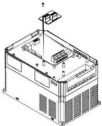
natural_image
Isometric technical line drawing of a server or chassis unit with internal components and mounting bracket (no text or symbols)Appendix B: Figure 1 Installation way of VFD-IO1
Function definition of wiring terminals:
Appendix B: Table 1 Functional descriptions of wiring terminals
| Category | Terminal symbol | Terminal name | Functional description |
| Power | +24V-COM | Connect +24V power externally | Provide +24V power externally, be used as working power of digital input/output terminal as well as power of external sensor; maximum current current: 200mA |
| OP2 | Power terminal of digital input | No power connection of OP2 when leaving factory, connect to external power based on demands | |
| Function digital input terminals | DI6-OP2 | Digital input 6 | 1. Opto-isolator: be compatible with bipolarinput2. Input impedance: DI6, DI7: 3.3kΩ, DI8:2.4kΩ3. Voltage range during level input: 9~30V4. DI6, DI7 are common input terminals, inputfrequency <100Hz; DI8 is high-speed pulse input terminal, max. input frequency <100kHz |
| DI7-OP2 | Digital input 7 | ||
| DI8-OP2 | Digital input 8 |
Appendix C: Instructions of expansion card for common encoder
(Apply to all series machines)
I. Introduction
VFD is equipped with expansion card for common encoder (namely PG card). As an optional accessory, it's necessary for closed-loop vector control of frequency convertor. Select corresponding PG card as per output way of encoder, and the specific models are as follows:
| Optional accessories | Description Other | |
| VFD-PG1 | Differential input of PG card without frequency dividing output | Terminal wiring |
| VFD-PG2 | PG card of rotary transformer | DB9 bus socket |
| VFD-PG3 | OC input of PG card, frequency dividing output at 1:1 | Terminal wiring |
II. Mechanical installation and functional descriptions of control terminals
- Installation way, appearance, specification and signal definition of wiring terminal can respectively refer to Figure 1 and Table 1 in Appendix C:
1) Please assemble and disassemble PG card after complete outage of frequency convertor;
2) Connect J3 on control panel with expansion card through 18pin FFC (ensure correct installation and proper snap joint).
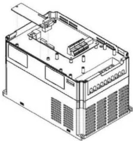
natural_image
Technical line drawing of an industrial electronic device with cooling fins and internal components (no text or symbols)Appendix E: Figure 1 Installation way of expansion card for encoder
Appendix C: Table 1 Specification and signal definitions of wiring terminals
| Differential PG card (VFD-PG1) | ||
| VFD-PG1 specification | ||
| User interface | Oblique cutting terminal | |
| Distance | 3.5mm | |
| Screw Straight | ||
| Pluggable No | ||
| Wire gauge | 16-26AWG | |
| Maximum rate | 500kHz | |
| Differential signal amplitude of input | ≤7V | |
| VFD-PG1 signal definition of wiring | ||
| No. Symbol Description | ||
| 1 A+ | Encoder output A signal + | |
| 2 A- | Encoder output A signal - | |
| 3 B+ | Encoder output B signal + | |
| 4 B- | Encoder output B signal- | |
| 5 Z+ | Encoder output Z signal + | |
| 6 Z- | Encoder output Z signal - | |
| 7 5V | Provide 5V/100mA power externally | |
| 8 COM | Power ground | |
| 9 PE | Shield terminal | |
| PG card of rotary transformer (VFD-PG2) | ||
| VFD-PG2 specification | ||
| User interface | DB9 female contact | |
| Pluggable Yes | ||
| Wire gauge | >22AWG | |
| Resolution ratio 12 digit | ||
| Driving frequency | 10kHz | |
| VRMS 7V | ||
| VP-P | 3.15±27% | |
| VFD-PG2 terminal | ||
| No. Symbol Description | ||
| 1 EXC1 | - driving of rotary transformer | |
| 2 | EXC | + driving of rotary transformer |
| 3 | SIN | + feedback SIN of rotary transformer |
| 4 | SINLO | - feedback SIN of rotary transformer |
| 5 | COS | + feedback COS of rotary transformer |
| 6-8 | - | - |
| 9 | COSLO | - feedback COS of rotary transformer |
VFD-PG3 specification
User interface Oblique cutting terminal
Distance
3.5mm
Screw Straight
Pluggable No
Wire gauge
16-26AWG
Maximum rate
100KHz
VFD-PG3 terminal
No. Symbol Description
| 1 | A Encoder output A signal | |
| 2 | B Encoder output B signal | |
| 3 | Z | Encoder output Z signal |
| 4 | 15V | Provide 15V/100mA power externally |
| 5 | COM | Power ground |
| 6 | COM | Power ground |
| 7 A1 | PG card feedback output A signal at 1:1 | |
| 8 B1 | PG card feedback output B signal at 1:1 | |
| 9 | PE | Shield terminal |
Appendix D: Instructions of CANlink communication expansion card (VFD-CAN1)
(Apply to all series)
I. Introduction
It's specially developed for CANlink communication function of this series frequency convertor.
II. Mechanical installation and functional descriptions of control terminals
- Installation way and appendix B: the same with IO expansion card (VFD-IO1). Functional descriptions of wiring terminals and jumper descriptions respectively refer to Figure 1, Table 1 and Table 2 in Appendix D:
Appendix D: Table 1 Functional description of control terminal
| Category | Terminal symbol | Terminal name | Functional description |
| CAN communication (CN1) | CANH/CANL | Communication interface terminal | CAN communication input terminal |
| COM | Power ground of CAN communication |
Appendix D: Table 2 Jumper description
Jumper No.
J2
Description
Select matched resistance for CAN terminal
Appendix E: Instructions of RS-485 communication expansion card (VFD-TX1)
(Apply to all series)
I. Introduction
It's specially developed for 485 communication function of this series frequency convertor. By adopting isolation scheme, electric parameters conform to international standard and users can select based on demands so as to control operation of frequency convertor and set parameters through remote serial port;
II. Mechanical installation and functional descriptions of control terminals
- Installation way and appendix B: the same with IO expansion card (VFD-IO1). Functional descriptions of wiring terminals and dial-up definitions respectively refer to Table 1 and Table 2 in Appendix E:
Functional description of control terminal:
Appendix E: Table 1 Functional description of control terminal
| Category Terminal | symbol | Terminal name | Functional description |
| 485 communication (CN1) | 485+/485- | Communication interface terminal | 485 communication input terminal, isolation input |
| CGND | Power ground of 485 communication | Isolated power |
Jumper description:
Appendix E: Table 2 Jumper description
| Jumper No. Description | |
| J1 | Select matched resistance for 485 terminal |
Note:
To prevent communication signal from external interference, communication wire can use twisted pair and avoid using parallel lines as far as possible;
Appendix F: VFD-Modbus communication protocol
This series frequency convertor provides RS232/RS485 communication interface and supports Modbus communication protocol. Users can realize centralized control through computer or PLC, set run command of frequency convertor through communication protocol, modify or read parameters of function code, read working condition and fault information of frequency convertor, etc.
I. Protocol content
The serial communication protocol defines transmissive information contents and using format of serial communication, including format for polling of host (or broadcast), encoding method of host such as function code of required action, transmission data and error verification, etc. The response of slave also adopts same structure and the contents include action confirmation, data return and error verification, etc. If any error of slave when receiving information or failure to finish the action required by host, the slave will organize a fault message as response feedback for the host.
Application mode: frequency convertor accesses to “single-host and multiple-slave” PC/PLC control network with RS232/RS485 bus.
Structure of bus
(1) Interface mode
RS232/RS485 hardware interface
(2) Transmission mode: asynchronous serial and half-duplex. For the host and slave at the same moment, one can only send data and another can only receive data. During serial asynchronous communication process, data is sent with the form of message frame by frame.
(3) Topological structure: single-host and multiple-slave system. The setting range of slave address is 1\~247 and 0 is address of broadcast communication. Slave address in network should be unique.
Protocol description
Communication protocol of this series frequency convertor is a kind of asynchronous serial master-slave Modbus communication protocol, and only one device (host) in the network can establish protocol (called as "query/command"). Other devices (slave) can only response the "query/command" of host by providing data or take corresponding actions based on "query/command" of host. Host refers to personal computer (PC), industrial control equipment or programmable logic controller (PLC), etc, and slave means this series frequency convertor. The host can not only communicate with certain slave separately, but issue broadcast information to all inferior slaves. For separately accessed "query/command" of host, the slave needs to return a message (called as response). For the broadcast information issued by the host, the slave does not need to feedback response to host.
Structure of communication materials: communication data format of modbus protocol for this series frequency convertor is as below:
For RTU mode, message sending starts with pause time for at least 3.5 characters. Diverse character time under network Baud rate is easily realized (as shown in below T1-T2-T3-T4). The first domain of transmission is equipment address.
The available transmission character is hexadecimal 0...9, A...F. Network equipment detects network bus constantly, including pausing interval time. When receiving first domain (address domain), each equipment will decode to judge if sending to own. After the last transmission character, the pause time of at least 3.5 characters marks the ending of message. A new message will start after the pause.
The whole message frame should be continuous streaming transfer. If the dwell time exceeds 1.5 characters before frame finishes, receiving equipment will refresh incomplete message and assume that next byte is address domain of a new message. Similarly, if a new message starts within time of 3.5 characters following previous message, receiving equipment will consider it as the delay of previous message, and then error will be caused, as it's impossible for the value of final CRC domain to be correct.
RTU frame format
| Frame header START | Time of 3.5 characters |
| Slave ADR Address | 1~247 |
| CMD code | 03: read slave parameters; 06: write slave parameters |
| DATA (N-1) | Data content: address of function code parameters, number of function code parameters, value of function code parameters, etc |
| DATA (N-2) | |
| ...... | |
| DATA0 | |
| CRC CHK high-order | Detection value: CRC value |
| CRC CHK low-order | |
| END | Time of 3.5 characters |
CMD and DATA
CMD code: 03H, read N word (12 words at most). For example: start address F002 of frequency convertor with slave address being 01 reads 2 values successively
CMD message of host
| ADR 01H | |
| CMD 03H | |
| Start address high-order | F0H |
| Start address low-order | 02H |
| Register No. high-order | 00H |
| Register No. low-order | 02H |
| CRC CHK high-order | CRC CHK value to be calculated |
| CRC CHK low-order |
Response message of slave
PD-05 is set as 0:
| ADR 01H | |
| CMD 03H | |
| Byte No. high-order 00H | |
| Byte No. low-order | 04H |
| Data F002Hhigh-order | 00H |
| Data F002Hlow-order | 00H |
| Data F003Hhigh-order | 00H |
| Data F003Hlow-order | 01H |
| CRC CHKlow-order | CRC CHK value to be calculated |
| CRC CHKhigh-order |
FD-05 is set as 1:
| ADR 01H | |
| CMD 03H | |
| Byte No. | 04H |
| Data F002Hhigh-order | 00H |
| Data F002Hlow-order | 00H |
| Data F003Hhigh-order | 00H |
| Data F003Hlow-order | 01H |
| CRC CHK low-order | CRC CHK value to be calculated |
| CRC CHK high-order |
CMD code: 06H, write one word. For example: write 5000 (1388H) in F00AH address of frequency convertor with slave address being 02H.
CMD message of host
| ADR 02H | |
| CMD 06H | |
| Data address high-order | F0H |
| Data address low-order | 0AH |
| Data content high-order | 13H |
| Data content low-order | 88H |
| CRC CHK low-order | CRC CHK value to be calculated |
| CRC CHK high-order |
Response message of slave
| ADR 02H | |
| CMD 06H | |
| Data address high-order | F0H |
| Data address low-order | 0AH |
| Data content high-order | 13H |
| Data content low-order | 88H |
| CRC CHK low-order | CRC CHK value to be calculated |
| CRC CHK high-order |
Verification mode-CRC verification mode: CRC (Cyclical Redundancy Check) uses RTU frame format, and message includes error detection domain based on CRC method. CRC domain detects the contents of whole message. CRC domain is two-byte and includes 16-bit binary system value. It's added to message after calculation by transmission equipment. Receiving equipment recalculates CRC of received message and compares with value in received CRC domain. If two CRC values are not equal, the transmission is wrong.
CRC firstly stores 0xFFFF, and then calls a course to process successive 8-bit bytes in message and value in current register. Only 8Bit data in each character is valid for CRC, start bit, stop bit and parity check bit are invalid.
During producing process of CRC, each 8-bit byte is XOR with register contents separately. Finally, it moves to the direction of least significant bit, and most significant bit is filled with 0. LSB is extracted for detection. If LSB is 1, register is XOR with preset value. If LSB is 0, no action. Repeat the whole process for 8 times. After last bit ( 8^th bit) finishes, next 8-bit byte is XOR with current value of register alone. The final value in register is CRC value after all bytes in message are executed.
When adding CRC to message, add low byte firstly and then high byte. Simple function of CRC is as below:
unsigned int crc_chk_value (unsigned char *data_value, unsigned char length) {
    unsigned int crc_value=0xFFFF;
    int i;
    while (length--) {
    crc_value^=*data_value++;
    for (i=0;i<8;i++) {
    if (crc_value&0x0001)
    {
    crc_value= (crc_value>>1)
    }
    else crc_value=crc_value>>1;
    {
    }
    }
    }
    return (crc_value);
}
Address definition of communication parameter
This part is communication content used for controlling operation of frequency convertor, setting state and related parameters of frequency convertor.
Read-write function code parameter (some function codes can't be modified, but are simply used or monitored by manufacturer).
Marking rules of function code parameter address:
Express rules with group No. and marking No. of function code being parameter address:
High byte: P0\~PF (P group), A0\~AF (A group), 70\~7F (U group); low byte: 00\~FF
E.g.: P3-12, address is expressed as P30C;
Note: PF group: neither read nor modify parameters;
U group: only read but not modify parameters.
When the frequency convertor is in running status, some parameters can't be modified. Some parameters can't be modified no matter what is the status of frequency convertor. When modifying the function code parameters, range, unit and related descriptions of parameters should be also noticed.
Besides, as EEPROM is frequently stored, it will reduce lifespan of EEPROM. Therefore, under communication mode, some function codes don't have to be stored, and only modify the value in RAM.
If it's P group parameter, changing high-order F of the function code address to be 0 can realize the function. If it's A group parameter, changing high-order A of the function code address to be 4 can realize the function. Corresponding function code address is expressed as below: high-order byte: 00\~0F (P group), 40\~4F (A group); low-order byte: 00\~FF
E.g.: function code P3-12 is not stored in EEPROM, the address is expressed as 030C; function code A0-05 is not stored in EEPROM, the address is expressed as 4005; the address can only write RAM and conduct read action. When reading, it's invalid address. For all parameters, CMD code 07H can also be used to realize the function.
When the frequency convertor is in running status, some parameters can't be modified. Some parameters can't be modified no matter what is the status of frequency convertor. When modifying the function code parameters, range, unit and related descriptions of parameters should be also noticed.
Halt/running parameters:
| Parameter address Parameter description | |
| 1000 | *Communication setting value (-10000~10000) (decimal system) |
| 1001 Running frequency | |
| 1002 Busbar voltage | |
| 1003 | Output voltage |
| 1004 Output current | |
| 1005 Output power | |
| 1006 | Output torque |
| 1007 Running speed | |
| 1008 | DI input mark |
| 1009 | DO output mark |
| 100A | AI1 voltage |
| 100B | AI2 voltage |
| 100C AI3 | voltage |
| 100D | Count value input |
| 100E | Length value input |
| 100F Loading speed | |
| 1010 | PID setting |
| 1011 | PID feedback |
| 1012 | PLC step |
| 1013 | PULSE frequency, unit 0.01kHz |
| 1014 | Feedback speed, unit 0.1Hz |
| 1015 Surplus running time | |
| 1016 | AI1 voltage before calibration |
| 1017 | AI2 voltage before calibration |
| 1018 | AI3 voltage before calibration |
| 1019 Linear speed | |
| 101A Current electrifying time | |
| 101B | Current running time |
| 101C | PULSE frequency, unit 1Hz |
| 101D | Communication setting value |
| 101E | Actual feedback speed |
| 101F | Principal frequency X display |
| 1020 | Auxiliary frequency Y display |
Note:
Communication setting value is percentage of relative value, namely 10000 corresponds to 100.00%, -10000 corresponds to -100.00%. For frequency dimension, this percent is the percentage of relatively largest frequency (P0-10). For the data of torque dimension, this percent is P2-10, A2-48, A3-48, A4-48 (upper limit setting of torque respectively corresponds to first and second motor).
Input command order to frequency convertor: (only write)
| Command word address Command function | |
| 2000 | 0001: foreward operation |
| 0002: reverse operation | |
| 0003: foreward inching | |
| 0004: reverse inching | |
| 0005: free halt | |
| 0006: deceleration halt | |
| 0007: fault reset | |
Read status of frequency convertor: (only read)
| Status word address | Status word function |
| 3000 | 0001: foreward operation |
| 0002: reverse operation | |
| 0003: halt |
Cryptographic check of parameter locking: (if returning to be 8888H, pass cryptographic check)
| Password address Contents of inputting password | |
| 1F00 ***** | |
| Command address Command contents | |
| 2001 | BIT0: DO1 output controlBIT1: DO2 output controlBIT2: RELAY1 output controlBIT3: RELAY2 output controlBIT4: FMR output controlBIT5: VDO1BIT6: VDO2BIT7: VDO3BIT8: VDO4BIT9: VDO5 |
Control of analog outputAO1: (only write)
| Command address Command contents | |
| 2002 | 0~7FFF means 0%~100% |
Control of analog output AO2: (only write)
| Command address Command contents | |
| 2003 | 0~7FFF means 0%~100% |
Control of PULSE output: (only write)
| Command address | Command contents |
| 2004 | 0~7FFF means 0%~100% |
Fault description of frequency convertor:
| Fault address Fault message | |
| 8000 | 0000: no fault0001: reserve0002: accelerated overcurrent0003: decelerated overcurrent0004: constant-speed overcurrent0005: accelerated overvoltage0006: decelerated overvoltage0007: constant-speed overvoltage0008: overload fault of buffer resistance0009: undervoltage fault000A: overload of frequency convertor000B: overload of motor000CL: default phase of input000D: default phase of output000E: overheating module000F: external fault0010: abnormal communication0011: abnormal contactor0012: current detection fault0013: motor tuning fault0014: fault of encoder/PG card0015: abnormal read-write of parameter0016: hardware fault of frequency convertor0017: to-ground short-circuit fault of motor0018: reserve0019: reserve001A: reach running time001B: user-defined fault 1001C: user-defined fault 2001D: reach electrifying time001E: off-load001F: PID feedback loss during operation0028: overtime fault of fast current-limiting0029: fault of motor switch during operation002A: too large velocity misalignment002B: supervelocity of motor002D: over-temperature of motor005A: wrong setting of line number of encoder005B: not connecting with encoder005C: error of initial position005E: error of velocity feedback |
| Communication fault address | Functional description of fault |
| 8001 | 0000: no fault0001: wrong password0002: wrong command code0003: wrong CRC verification0004: invalid address0005: invalid parameter0006: invalid parameter alternation0007: system is locked0008: EEPROM operation is proceeding |
Description of PD group communication parameters
| Pd-00 | Baud rate | Factory default | 6005 |
| Setting range | Unit: MODUBS Baud rate0: 300BPS1: 600BPS2: 1200BPS3: 2400BPS4: 4800BPS5: 9600BPS6: 19200BPS7: 38400BPS8: 57600BPS9: 115200BPS | ||
The parameter is used to set data transmission rate between host computer and frequency convertor. Please note that the Baud rate of host computer and frequency convertor should be consistent. Otherwise, communication is unable to proceed. The larger the Baud rate, the faster the communication speed.
| Fd-01 | Data format | Factory default | 0 |
| Setting range | 0: no verification: data format <8,N,2>1: even verification: data format <8,E,1>2: odd verification: data format <8,O,1>3: no verification: data format <8-N-1> | ||
The data format of host computer and frequency convertor should be consistent. Otherwise, communication is unable to proceed.
| Pd-02 | Local address | Factory default | 1 |
| Setting range | 1~247, 0 is broadcast address | ||
If local address is set as 0, namely broadcast address, broadcast function of host computer can be realized.
Local address is unique (apart from broadcast address), and it's the basis to realize point-to-point communication between host computer and frequency convertor.
| Pd-03 | Response delay | Factory default | 2ms |
| Setting range | 0~20ms | ||
Response delay: interval time between ending time of data reception of frequency converter and time of sending data of host computer. If response delay is shorter than system processing time, response delay takes system processing time as criterion. If response delay is longer than system
processing time, delay await is required after system processes data. After reaching response delay time, data will be sent to host computer.
| Pd-04 | Communication overtime | Factory default | 0.0 s |
| Setting range | 0.0 s (invalid)0.1~60.0s | ||
If function code is set to be 0.0s, parameter of communication overtime is invalid.
If function code is set to be valid value, interval time between one communication and next communication exceeds communication overtime, the system will give alarm of communication fault (Err 16). Under normal conditions, it's set to be invalid. If setting subparameter in the system of continuous communication, communication status can be monitored.
| Pd-05 | Communication protocol Factory default | 0 |
| Setting range | 0: non-standard Modbus protocol1: Standard Modbus protocol |
PD-05=1: select standard Modbus protocol.
PD-05=0: when reading command, number of bytes returned by slave has one more byte than standard Modbus protocol. See details in “5 communication data structure” of the protocol.
| Pd-05 | Communication reads current resolution | Factory default | 0 |
| Setting range | 0: 0.01A1: 0.1A | ||
It's used to confirm output unit of current value when communication reads output current.
Wprowadzenie

natural_image
Technical line drawing of a rectangular enclosure with dimensions labeled H, D, and H1 (no text or symbols beyond labels)Montaż korpusu

natural_image
Line drawing of two identical rectangular electronic devices with control panels and indicator lights (no text or symbols)natural_image
Line drawing of a multi-tiered industrial machine or server unit (no text or symbols visible)natural_image
Technical line drawing of an electronic device with internal components and mounting holes (no text or symbols)line
| czas | Częstotliwość sygnału detekcji | | ---- | ------------------------------- | | 0 | ON | | 1 | ON | | 2 | ON | | 3 | ON | | 4 | ON | | 5 | ON | | 6 | ON | | 7 | ON | | 8 | ON | | 9 | ON | | 10 | ON | | 11 | ON | | 12 | ON | | 13 | ON | | 14 | ON | | 15 | ON | | 16 | ON | | 17 | ON | | 18 | ON | | 19 | ON | | 20 | ON | | 21 | ON | | 22 | ON | | 23 | ON | | 24 | ON | | 25 | ON | | 26 | ON | | 27 | ON | | 28 | ON | | 29 | ON | | 30 | ON | | 31 | ON | | 32 | ON | | 33 | ON | | 34 | ON | | 35 | ON | | 36 | ON | | 37 | ON | | 38 | ON | | 39 | ON | | 40 | ON | | 41 | ON | | 42 | ON | | 43 | ON | | 44 | ON | | 45 | ON | | 46 | ON | | 47 | ON | | 48 | ON | | 49 | ON | | 50 | ON | | 51 | ON | | 52 | ON | | 53 | ON | | 54 | ON | | 55 | ON | | 56 | ON | | 57 | ON | | 58 | ON | | 59 | ON | | 60 | ON | | 61 | ON | | 62 | ON | | 63 | ON | | 64 | ON | | 65 | ON | | 66 | ON | | 67 | ON | | 68 | ON | | 69 | ON | | 70 | ON | | 71 | ON | | 72 | ON | | 73 | ON | | 74 | ON | | 75 | ON | | 76 | ON | | 77 | ON | | 78 | ON | | 79 | ON | | 80 | ON | | 81 | ON | | 82 | ON | | 83 | ON | | 84 | ON | | 85 | ON | | 86 | ON | | 87 | ON | | 88 | ON | | 89 | ON | | 90 | ON | | 91 | ON | | 92 | ON | | 93 | ON | | 94 | ON | | 95 | ON | | 96 | ON | | 97 | ON | | 98 | ON | | 99 | ON | | 100 | ON |line
| czas | Prąd wyjściowy | Sygnał wykrycia przekroczenia prądu wyjściowego | |------|----------------|--------------------------------------------------| | 0 | Low | 0 | | 1 | High | 0 | | 2 | Medium | 0 | | 3 | Low | 0 | | 4 | High | 0 | | 5 | Medium | 0 | | 6 | Low | 0 | | 7 | High | 0 | | 8 | Medium | 0 | | 9 | Low | 0 | | 10 | High | 0 | | 11 | Medium | 0 | | 12 | Low | 0 | | 13 | High | 0 | | 14 | Medium | 0 | | 15 | Low | 0 | | 16 | High | 0 | | 17 | Medium | 0 | | 18 | Low | 0 | | 19 | High | 0 | | 20 | Medium | 0 | | 21 | Low | 0 | | 22 | High | 0 | | 23 | Medium | 0 | | 24 | Low | 0 | | 25 | High | 0 | | 26 | Medium | 0 | | 27 | Low | 0 | | 28 | High | 0 | | 29 | Medium | 0 | | 30 | Low | 0 | | 31 | High | 0 | | 32 | Medium | 0 | | 33 | Low | 0 | | 34 | High | 0 | | 35 | Medium | 0 | | 36 | Low | 0 | | 37 | High | Low | | 38 | Medium | 0 | | 39 | Low | 0 | | 40 | High | Low | | 41 | Medium | Low | | 42 | Low | Low | | 43 | High | Low | | 44 | Medium | Low | | 45 | Low | Low | | 46 | High | Low | | 47 | Medium | Low | | 48 | Low | Low | | 49 | High | Low | | 50 | Medium | Low | | 51 | Low | Low | | 52 | High | Low | | 53 | Medium | Low | | 54 | Low | Low | | 55 | High | Low | | 56 | Medium | Low | | 57 | Low | Low | | 58 | High | Low | | 59 | Medium | Low | | 60 | Low | Low | | 61 | High | Low | | 62 | Medium | Low | | 63 | Low | Low | | 64 | High | Low | | 65 | Medium | Low | | 66 | Low | Low | | 67 | High | Low | | 68 | Medium | Low | | 69 | Low | Low | | 70 | High | Low | | 71 | Medium | Low | | 72 | Low | Low | | 73 | High | Low | | 74 | Medium | Low | | 75 | Low | Low | | 76 | High | Low | | 77 | Medium | Low | | 78 | Low | Low | | 79 | High | Low | | 80 | Medium | Low | | 81 | Low | Low | | 82 | High | Low | | 83 | Medium | Low | | 84 | Low | Low | | 85 | High | Low | | 86 | Medium | Low | | 87 | Low | Low | | 88 | High | Low | | 89 | Medium | Low | | 90 | Low | Low | | 91 | High | Low | | 92 | Medium | Low | | 93 | Low | Low | | 94 | High | Low | | 95 | Medium | Low | | 96 | Low | Low | | 97 | High | Low | | 98 | Medium | Low | | 99 | Low | Low | | P8-36 (Limit prądu wyjściowego) / Czas opóźnienia wykrycia przekroczenia prądu wyjściowego P8-37 (Czas opóźnienia wykrycia przekroczenia prądu wyjściowego P8-37)line
| czas | wyjściowa | | ---- | --------- | | 0 | 0 | | Początkowa PID PA-21 | 0 | | 0 | 1 | | 0 | 1 | | 0 | 1 | | 0 | 1 | | 0 | 1 | | 0 | 1 | | 0 | 1 | | 0 | 1 | | 0 | 1 | | 0 | 1 | | 0 | 1 | | 0 | 1.5 | | 0 | 1.5 | | 0 | 1.5 | | 0 | 1.5 | | 0 | 1.5 | | 0 | 1.5 | | 0 | 1.5 | | 0 | 1.5 | | 0 | 1.5 | | 0 | 1.5 |natural_image
Technical line drawing of an electronic device chassis with ventilation grilles and mounting brackets (no text or symbols)natural_image
Isometric line drawing of an electronic device chassis with visible internal components and mounting bracket (no text or symbols)natural_image
Technical line drawing of an industrial electronic device casing with internal components and ventilation grilles (no text or symbols)natural_image
Technical line drawing of two identical electrical cabinet designs (no text or symbols)natural_image
Line drawing of a multi-tiered industrial or electronic device with no visible text or symbolsnatural_image
Technical line drawing of an electronic device with internal components and mounting holes (no text or symbols)line
| Frequency Range | Jump Frequency Range | |---|---| | Jump frequency range | 0 to 1 | | Jump frequency range | 1 to 2 |line
| čas | Value | | --- | --- | | Start | 0 | | Peak | ~0.8 | | Midpoint | ~0.2 | | End | ~0.9 |line
| čas | Výstupní proud | | --- | --- | | 0 | 0 | | 1 | Low | | 2 | Medium | | 3 | High | | 4 | Medium-High | | 5 | Low | | 6 | Medium | | 7 | High | | 8 | Low | | 9 | Medium | | 10 | High | | 11 | Low | | 12 | Medium | | 13 | High | | 14 | Low | | 15 | Medium | | 16 | High | | 17 | Low | | 18 | Medium | | 19 | High | | 20 | Low | | 21 | Medium | | 22 | High | | 23 | Low | | 24 | Medium | | 25 | High | | 26 | Low | | 27 | Medium | | 28 | High | | 29 | Low | | 30 | Medium | | 31 | High | | 32 | Low | | 33 | Medium | | 34 | High | | 35 | Low | | 36 | Medium | | 37 | High | | 38 | Low | | 39 | Medium | | 40 | High | | 41 | Low | | 42 | Medium | | 43 | High | | 44 | Low | | 45 | Medium | | 46 | High | | 47 | Low | | 48 | Medium | | 49 | High | | 50 | Low | | 51 | Medium | | 52 | High | | 53 | Low | | 54 | Medium | | 55 | High | | 56 | Low | | 57 | Medium | | 58 | High | | 59 | Low | | 60 | Medium | | 61 | High | | 62 | Low | | 63 | Medium | | 64 | High | | 65 | Low | | 66 | Medium | | 67 | High | | 68 | Low | | 69 | Medium | | 70 | High | | 71 | Low | | 72 | Medium | | 73 | High | | 74 | Low | | 75 | Medium | | 76 | High | | 77 | Low | | 78 | Medium | | 79 | High | | 80 | Low | | 81 | Medium | | 82 | High | | 83 | Low | | 84 | Medium | | 85 | High | | 86 | Low | | 87 | Medium | | 88 | High | | 89 | Low | | 89.5 | Medium | | 90.5 | High | | 91.5 | Low | | 92.5 | Medium | | 93.5 | High | | 94.5 | Low | | 95.5 | Medium | | 96.5 | High | | 97.5 | Low | | 98.5 | Medium | | 99.5 | High | | 100.5 | Low |natural_image
Technical line drawing of an electronic device chassis with visible internal components and mounting brackets (no text or labels)natural_image
Isometric line drawing of a server rack unit with internal components and mounting bracket (no text or labels)Montage du corps
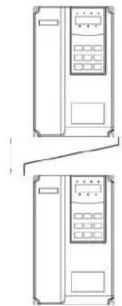
natural_image
Technical line drawing of two identical electrical cabinet designs (no text or symbols)natural_image
Line drawing of a multi-tiered industrial machine or server unit (no text or symbols visible)natural_image
Technical line drawing of an electronic device with internal components and mounting holes (no text or symbols)Figure 3-7 Wiring diagram of analog input terminal
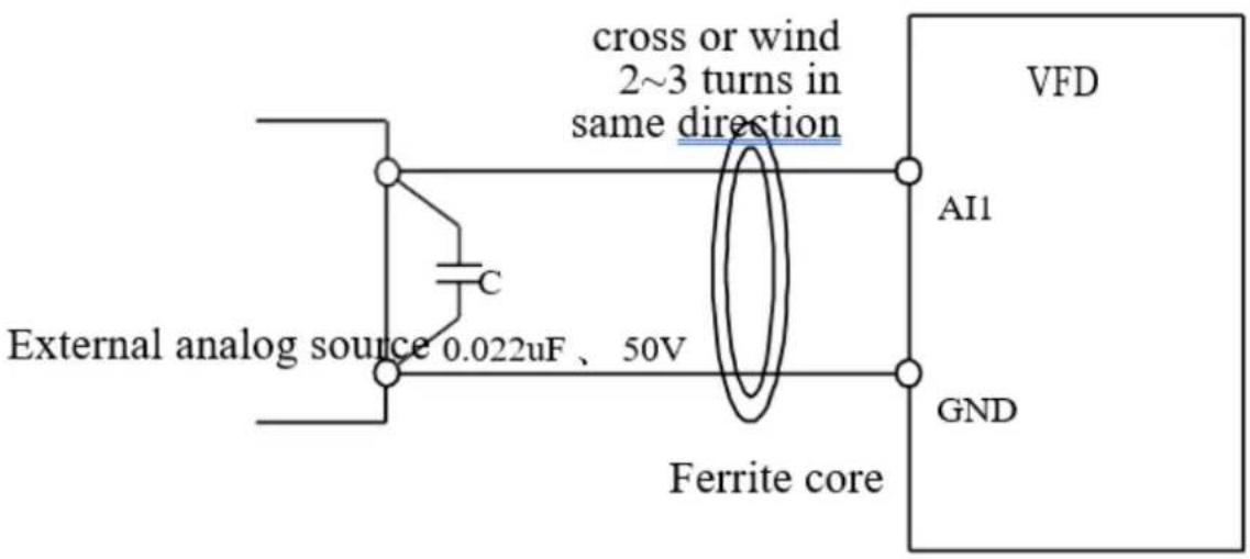
Contrôleur externe
line
| Output frequency | Output voltage | | ---------------- | -------------- | | V1 | V1 | | Vb | Vb | | f1 | V1 | | fb | Vb |line
| Phase | Tension Vb w % | |---|---| | V1 | V1 | | V2 | V3 | | F2 | V2 | | F3 | V3 | | Fb | V3 || K1 | K2 | Run command |
| 0 | 0 | Step |
| 0 | 1 | Reversion |
| 1 | 0 | Forward |
| 1 | 1 | Stop |
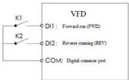
flowchart
graph TD
    K1 --> D11["Forward run (PWD)"]
    K2 --> D12["Reverse running (REV)"]
    COM --> D12
    D11 --> VFD
    D12 --> VFD
    COM --> VFD
| K1 | K2 | Run command |
| 0 | 0 | Stop |
| 0 | 1 | Reversion |
| 1 | 0 | Forward |
| 1 | 1 | Stop |
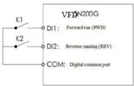
flowchart
graph TD
    A["SB2"] --> B["DI1"]
    C["SB1"] --> D["DI3"]
    E["SB3"] --> F["DI2 Reverse run (REV)"]
    B --> G["VFD Forward running (FWD)"]
    D --> H["Three line operation control"]
    F --> I["COM Digital public end"]
line
Corresponding to the setting (Frequency, rotational speed) | Frequency, rotational speed | AI | | :--- | :--- | | 100.0% | 0V(0mA) | | 10V(20mA) | 10V(20mA) |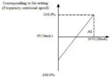
line
Corresponding to the setting (Frequency, rotational speed) | Frequency | Rotation Speed | | :--- | :--- | | 0V(0mA) | -100.0% | | 10V(20mA) | 100.0% |line
| Time | Value | |------|-------| | t1 | 0 | | t2 | Peak | | t1 | 0 | | t2 | 0 |Temps t
Fig. 6-11 Courbe S, A
| P7-03 | LED display running parameters 1 | Factory default | 1F | ||
| Setting range | 0000~FFFF | 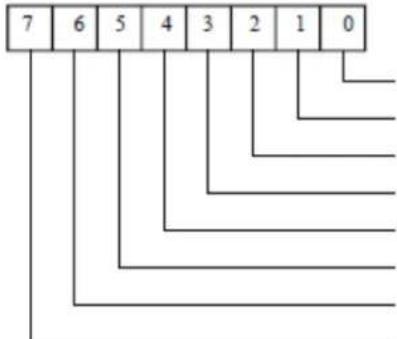 | Running frequency 1 (Hz)Set frequency (Hz)Bus voltage (V)Output voltage (V)Output current (A)Output power (kW)Output torque (%)DI input status (V)DO output statusAI1 voltage (V)AI2 voltage (V)AI3 voltage (V)Count valueLength valueLoad speed displayPID settingIf a parameter needs to be displayed during the running, set the corresponding bit to 1, and set P7-03 to the hexadecimal equivalent of this binary number. | ||
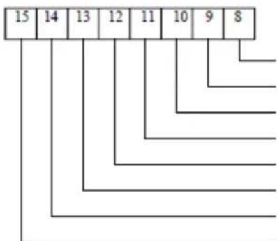 | |||||
| P7-04 | LED display running parameters 2 | Factory default | 0 | ||
| Setting range | 0000~FFFF | 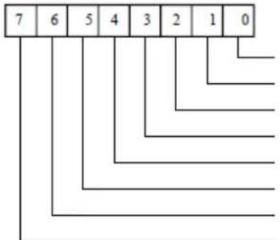 | PID feedbackPLC stagePulse setting frequency (kHz)Running frequency 2Remaining running timeAI1 voltage before correctionAI2 voltage before correctionAI3 voltage before correctionLinear speedCurrent power-on time (Hour)Current running time (Minute)Pulse setting frequency (Hz)Communication setting valueEncoder feedback speed (Hz)Main frequency X display (Hz)Auxiliary frequency Y display (Hz)If a parameter needs to be displayed during the running, set the corresponding bit to 1, and set P7-04 to the hexadecimal equivalent of this binary number. | ||
line
| Time | Frequency (Hz) | Detection Amplitude (dBm) | |------|----------------|---------------------------| | 0 | Low | 0 | | 1 | Medium | High | | 2 | High | Medium | | 3 | High | Low | | 4 | Low | 0 | | 5 | Low | 0 |line
| time | Value | |------|-------| | 0 | 0 | | Peak | High | | Low | Low | | ON | On |line
| temps | Courant de sortie | |-------|-------------------| | 0 | 0 | | Peak 1| High | | Peak 2| Medium | | Peak 3| Low | | Peak 4| High | | Peak 5| Medium | | Peak 6| Low | | Peak 7| High | | Peak 8| Medium | | Peak 9| Low |natural_image
Technical line drawing of an electronic device chassis with visible internal components and mounting brackets (no text or labels)natural_image
Technical line drawing of an internal electronic device casing with cooling fins and mounting brackets (no text or symbols)natural_image
Technical line drawing of a mechanical or electronic device with no visible text, numbers, or symbols.natural_image
Technical line drawing of an electronic device with internal components and mounting holes (no text or symbols)6-7 ábra Bilineáris mód 2
COM digital public end
line
| time | value | |------|-------| | Start | 0 | | Peak | High | | Mid | Low | | End | High |idő
natural_image
Technical line drawing of an electronic device chassis with ventilation grilles and mounting brackets (no text or symbols)natural_image
Isometric line drawing of a server rack unit with ventilation grilles and mounting bracket (no text or labels)natural_image
Technical line drawing of an industrial electronic device casing with internal components and mounting brackets (no text or symbols)Figur 2-8 Dimensionsritning av extern likströmsreaktor
Uncoil/Coil ---- 20 \~30%
Centrifug---- 50%\~60%
Tillfällig
bromsbelastning---- 5%
10% i allmänhet