FTL410QE3C - Module optique Finisar - Free user manual and instructions
Find the device manual for free FTL410QE3C Finisar in PDF.

| Product Type | 40GBASE-LR4 QSFP+ Optical Transceiver |
| Brand | Finisar |
| Model | FTL410QE3C |
| Form Factor | QSFP+ |
| Data Rate | 40 Gbps |
| Fiber Type | Single-mode (SMF) |
| Wavelength | 4 x LAN WDM: 1270, 1290, 1310, 1330 nm |
| Transmission Distance | Up to 10 km |
| Connector Type | LC Duplex |
| Dimensions (W x H x D) | Approx. 70 x 18.8 x 8.5 mm |
| Weight | 150 g |
| Power Supply | 3.3 V DC |
| Power Consumption | <3.5 W |
| Operating Temperature | 0 to 70 °C |
| Storage Temperature | -40 to 85 °C |
| Laser Safety | Class 1 Laser Product (IEC 60825) |
| Compliance | IEEE 802.3ba, QSFP+ MSA |
| Hot-Pluggable | Yes |
| Digital Diagnostic Monitoring (DDM) | Supported |
| Maintenance | Clean optical connectors with lint-free wipes and isopropyl alcohol |
| Spare Parts | Not applicable (integrated module) |
Frequently Asked Questions - FTL410QE3C Finisar
User questions about FTL410QE3C Finisar
0 question about this device. Answer the ones you know or ask your own.
Ask a new question about this device
Download the instructions for your Module optique in PDF format for free! Find your manual FTL410QE3C - Finisar and take your electronic device back in hand. On this page are published all the documents necessary for the use of your device. FTL410QE3C by Finisar.
USER MANUAL FTL410QE3C Finisar
Product Specification
40BASE-SR4 QSFP+ Gen3 Optical Transceiver Module
FTL410QE3C
PRODUCT FEATURES
- Four-channel full-duplex transceiver module
• Hot Pluggable QSFP+ form factor
• Maximum link length of 100m on OM3 Multimode Fiber (MMF) and 150m on OM4 MMF - Multirate capability: 1.06Gb/s to 10.5Gb/s per channel
- Unretimed XLPPI electrical interface
• Max power dissipation <1.2W
• Reliable VCSEL array technology
• Built-in digital diagnostic functions, including optical power monitoring
• Commercial operating case temperature range: 0°C to 70°C
• Single 1x12 MPO receptacle - RoHS-6 Compliant
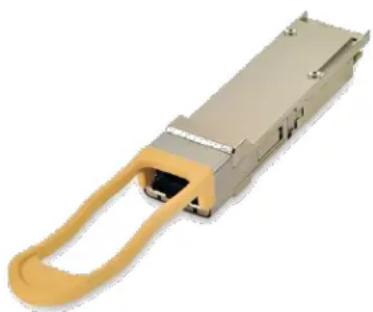
natural_image
3D rendering of a gray rectangular electronic device with a yellow strap-like connector (no text or symbols visible)APPLICATIONS
• 40GBASE-SR4 40G Ethernet
- Breakout to 4 x 10GBASE-SR Ethernet
• Proprietary interconnections
Finisar's FTL410QE3C QSFP+ transceiver modules are designed for use in 40 Gigabit per second links over multimode fiber. They are compliant with the QSFP+ MSA ^1,2 and IEEE 802.3ba 40GBASE-SR4 ^3 and breakout to 4 10GBASE-SR. Digital diagnostics functions are available via an I2C interface, including Tx and Rx power monitoring. The optical transceiver is compliant per the RoHS Directive 2011/65/EU ^4 . See Finisar Application Note AN-2038 for more details ^5 .
PRODUCT SELECTION
FTL410QE3C
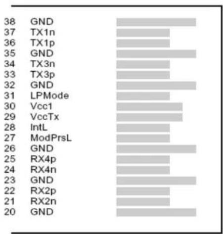
I. Pin Descriptions
bar
| Category | Value | |---|---| | 38 | GND | | 37 | TX1n | | 36 | TX1p | | 35 | GND | | 34 | TX3n | | 33 | TX3p | | 32 | GND | | 31 | LPMode | | 30 | Vcc1 | | 29 | VccTx | | 28 | IntlL | | 27 | ModPrsL | | 26 | GND | | 25 | RX4p | | 24 | RX4n | | 23 | GND | | 22 | RX2p | | 21 | RX2n | | 20 | GND |Top Side
Viewed from Top
Cared Edge
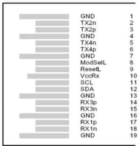
bar
| Gene | Value | |---|---| | GND | 1 | | TX2n | 2 | | TX2p | 3 | | GND | 4 | | TX4n | 5 | | TX4p | 6 | | GND | 7 | | ModSelL | 8 | | ResetL | 9 | | VccRx | 10 | | SCL | 11 | | SDA | 12 | | GND | 13 | | RX3p | 14 | | RX3n | 15 | | GND | 16 | | RX1p | 17 | | RX1n | 18 | | GND | 19 |Bottom Side Viewed from Bottom
Figure 1 - QSFP+ MSA-compliant 38-pin connector
| Pin | Symbol | Name/Description | Notes |
| 1 | GND | Ground | 1 |
| 2 | Tx2n | Transmitter Inverted Data Input | |
| 3 | Tx2p | Transmitter Non-Inverted Data Input | |
| 4 | GND | Ground | 1 |
| 5 | Tx4n | Transmitter Inverted Data Input | |
| 6 | Tx4p | Transmitter Non-Inverted Data Input | |
| 7 | GND | Ground | 1 |
| 8 | ModSelL | Module Select | |
| 9 | ResctL | Module Reset | |
| 10 | Vcc Rx | +3.3 V Power supply receiver | |
| 11 | SCL | 2-wire serial interface clock | |
| 12 | SDA | 2-wire serial interface data | |
| 13 | GND | Ground | 1 |
| 14 | Rx3p | Receiver Non-Inverted Data Output | |
| 15 | Rx3n | Receiver Inverted Data Output | |
| 16 | GND | Ground | 1 |
| 17 | Rx1p | Receiver Non-Inverted Data Output | |
| 18 | Rx1n | Receiver Inverted Data Output | |
| 19 | GND | Ground | 1 |
| 20 | GND | Ground | 1 |
| 21 | Rx2n | Receiver Inverted Data Output | |
| 22 | Rx2p | Receiver Non-Inverted Data Output | |
| 23 | GND | Ground | 1 |
| 24 | Rx4n | Receiver Inverted Data Output | |
| 25 | Rx4p | Receiver Non-Inverted Data Output | |
| 26 | GND | Ground | 1 |
| 27 | ModPrsL | Module Present | |
| 28 | IntL | Interrupt | |
| 29 | Vcc Tx | +3.3 V Power supply transmitter | |
| 30 | Vcc1 | +3.3 V Power Supply | |
| 31 | LPMode | Low Power Mode | |
| 32 | GND | Ground | 1 |
| 33 | Tx3p | Transmitter Non-Inverted Data Input | |
| 34 | Tx3n | Transmitter Inverted Data Input | |
| 35 | GND | Ground | 1 |
| 36 | Tx1p | Transmitter Non-Inverted Data Input | |
| 37 | Tx1n | Transmitter Inverted Data Input | |
| 38 | GND | Ground | 1 |
Notes
- Circuit ground is internally isolated from chassis ground.
II. General Product Characteristics
| Parameter | Value | Unit | Notes |
| Module Form Factor | QSFP+ | ||
| Number of Lanes | 4 Tx and 4 Rx | ||
| Maximum Aggregate Data Rate | 42.0 | Gb/s | |
| Maximum Data Rate per Lane | 10.5 | Gb/s | Higher bit rates may be supported.Please contact Finisar. |
| Protocols Supported | Typical applications include 40G Ethernet, Infiniband QDR, SATA/SAS3 | This module is not retimed | |
| Electrical Interface and Pin-out | 38-pin edge connector | Pin-out as defined by the QSFP+ MSA ^2 | |
| Maximum Power Consumption | 1.2 | Watts | Varies with output voltage swing and pre-emphasis settings |
| Management Interface | Serial, I2C-based, 400 kHz maximum frequency | As defined by the QSFP+ MSA ^2 |
| Data Rate Specifications | Symbol | Min | Typ | Max | Units | Ref. |
| Bit Rate per Lane | BR | 1062 | 10500 | Mb/sec | 1 | |
| Bit Error Ratio | BER | 10^12 | 2 | |||
| Link distance on OM3 MMF | d | 100 | meters | 3 | ||
| Link distance on OM4 MMF | d | 150 | meters | 3 |
Notes:
- Compliant with 40G Ethernet. Compatible with 1/10 Gigabit Ethernet and 1/2/4/8/10G Fibre Channel.
- Tested with a PRBS 2 ^31 -1 test pattern.
- Per 40GBASE-SR4, IEEE 802.3ba
III. Absolute Maximum Ratings
| Parameter | Symbol | Min | Typ | Max | Unit | Ref. |
| Maximum Supply Voltage | Vcc1, VccTx, VccRx | -0.5 | 3.6 | V | ||
| Storage Temperature | T_S | -40 | 85 | °C | ||
| Case Operating Temperature | T_OP | 0 | 70 | °C | ||
| Relative Humidity | RH | 0 | 85 | % | 1 | |
| Damage Threshold, per Lane | DT | 3.4 | dBm |
Notes:
1. Non-condensing.
IV. Electrical Characteristics (T op = 0 to 70^,V_CC = 3.15 to 3.45 Volts)
| Parameter | Symbol | Min | Typ | Max | Unit | Ref. |
| Supply Voltage | Vcc1, VccTx, VccRx | 3.15 | 3.45 | V | ||
| Supply Current | Icc | 350 | mA | |||
| Link turn-on time | ||||||
| Transmit turn-on time | 2000 | ms | 2 | |||
| Transmitter (per Lane) | ||||||
| Single ended input voltage tolerance | VinT | -0.3 | 4.0 | V | ||
| Differential data input swing | Vin,pp | 180 | 1200 | mVpp | 3 | |
| Differential input threshold | 50 | mV | ||||
| AC common mode input voltage tolerance (RMS) | 15 | mV | ||||
| Differential input return loss | Per IEEE P802.3ba, Section 86A.4.1.1 | dB | 4 | |||
| J2 Jitter Tolerance | Jt2 | 0.17 | UI | |||
| J9 Jitter Tolerance | Jt9 | 0.29 | UI | |||
| Data Dependent Pulse Width Shrinkage | DDPWS | 0.07 | UI | |||
| Eye mask colorinates {X1, X2 Y1, Y2} | 0.11, 0.31 95, 350 | UI mV | 5 | |||
| Receiver (per Lane) | ||||||
| Single-ended output voltage | -0.3 | 4.0 | V | |||
| Differential data output swing | Vout,pp | 0 | 800 | mVpp | 6.7 | |
| AC common mode output voltage (RMS) | 7.5 | mV | ||||
| Termination mismatch at 1 MHx | 5 | % | ||||
| Differential output return loss | Per IEEE P802.3ba, Section 86A.4.2.1 | dB | 4 | |||
| Common mode output return loss | Per IEEE P802.3ba, Section 86A.4.2.2 | dB | 4 | |||
| Output transition time, 20% to 80% | 28 | ps | ||||
| J2 Jitter output | Jo2 | 0.42 | UI | |||
| J9 Jitter output | Jo9 | 0.65 | UI | |||
| Eye mask coordinates #1 {X1, X2 Y1, Y2} | 0.29, 0.5 150, 425 | UI mV | 5 | |||
| Power Supply Ripple Tolerance | PSR | 50 | mVpp | |||
Notes:
1. Maximum total power value is specified across the full temperature and voltage range.
- From power-on and end of any fault conditions.
- After internal AC coupling. Self-biasing 100Ω differential input.
- 10 MHz to 11.1 GHz range
- Hit ratio = 5 x 10E-5.
- AC coupled with 100Ω differential output impedance.
- Settable in 4 discrete steps via the I2C interface.
V. Optical Characteristics (T OP = 0 to 70°C, VCC = 3.15 to 3.45 Volts)
| Parameter | Symbol | Min | Typ | Max | Unit | Ref. |
| Transmitter (per Lane) | ||||||
| Signaling Speed per Lane | 10.5 | GBd | 1 | |||
| Center wavelength | 840 | 860 | nm | |||
| RMS Spectral Width | SW | 0.65 | nm | |||
| Average Launch Power per Lane | TXPx | -7.6 | -1.0 | dBm | ||
| Transmit OMA per Lane | TxOMA | -5.6 | 3.0 | dBm | 2 | |
| Difference in Power between any two lanes [OMA] | DPx | 4.0 | dB | |||
| Peak Power per Lane | PPx | 4.0 | dBm | |||
| Launch Power [OMA] minus TDP per Lane | P-TDP | -6.5 | dBm | |||
| TDP per Lane | TDP | 3.5 | dBm | |||
| Optical Extinction Ratio | ER | 3.0 | dB | |||
| Optical Return Loss Tolerance | ORL | 12 | dB | |||
| Encircled Flux | FLX | >86% at 19 um<30% at 4.5 um | dBm | |||
| Average launch power of OFF transmitter, per lane | -30 | dBm | ||||
| Relative Intensity Noise | RIN | -128 | dB/Hz | |||
| Transmitter eye mask definition {X1, X2, X3, Y1, Y2, Y3} | 0.23, 0.34, 0.43, 0.27, 0.35, 0.4 | |||||
| Receiver (per Lane) | ||||||
| Signaling Speed per Lane | 10.5 | GBd | 3 | |||
| Center wavelength | 840 | 860 | nm | |||
| Damage Threshold | DT | 3.4 | dBm | |||
| Average Receive Power per Lane | RXP_x | -9.9 | 2.4 | dBm | ||
| Receive Power (OMA) per Lane | RxOMA | 3.0 | dBm | |||
| Stressed Receiver Sensitivity (OMA) per Lane | SRS | -5.4 | dBm | |||
| Peak Power, per lane | PP_x | 4 | dBm | |||
| Receiver Reflectance | Rfl | -12 | dB | |||
| Vertical eye closure penalty, per lane | 1.9 | dB | ||||
| Stressed eye J2 jitter, per Lane | 0.3 | UI | ||||
| Stressed eye J9 jitter, per Lane | 0.47 | UI | ||||
| OMA of each aggressor lane | -0.4 | dBm | ||||
| Rx jitter tolerance: Jitter frequency and p-p amplitude | (75, 5) | kHz, UI | ||||
| (375, 1) | kHz, UI | |||||
| LOS De-Assert | LOS_D | -12 | dBm | |||
| LOS Assert | LOS_A | -30 | dBm | |||
| LOS Hysteresis | 0.5 | dBm | ||||
Notes:
1. Transmitter consists of 4 lasers operating at a maximum rate of 10.5Gb/s each.
2. Even if TDP is <0.9dB, the OMA min must exceed this value.
3. Receiver consists of 4 photodetectors operating at a maximum rate of 10.5Gb/s each.
VI. Memory Map and Control Registers
Compatible with the SFF-8436 QSFP+ MSA ^1 and the SFF-8636 Common Management Interface MSA. ^2 See Finisar Application Note AN-2119 ^6 for a complete EEPROM memory map.
VII. Environmental Specifications
Finisar FTL410QE3C transceivers have an operating temperature range from 0^ C to +70^ C case temperature.
| Environmental Specifications | Symbol | Min | Typ | Max | Units | Ref. |
| Case Operating Temperature | T_op | 0 | 70 | °C | ||
| Storage Temperature | T_sto | -40 | 85 | °C |
VIII. Regulatory Compliance
Finisar FTL410QE3C transceivers are RoHS-6 Compliant. Copies of certificates are available at Finisar Corporation upon request.
FTL410QE3C transceiver modules are Class 1 laser eye safety compliant per IEC 60825-1, which means that they are eye safe under normal “unaided” viewing conditions. Laser radiation may be hazardous if viewed with magnifying optics.
IX. Mechanical Specifications
The FTL410QE3C mechanical specifications are compliant to the QSFP+ MSA transceiver module specifications.
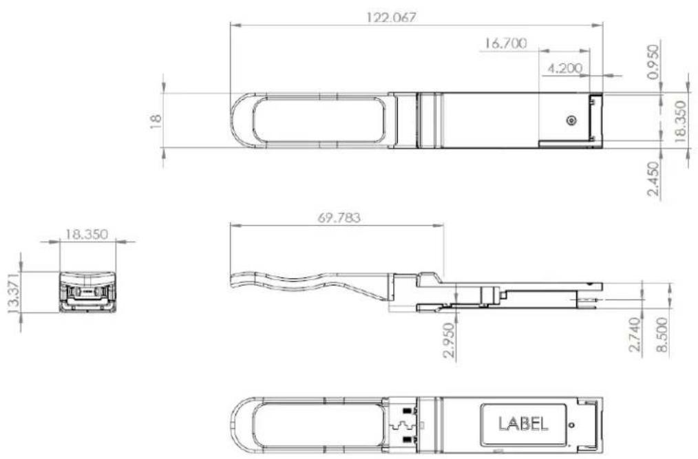
Figure 2 - FTL410QE3C mechanical drawing
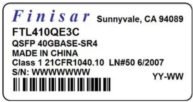
Figure 3 - FTL410QE3C product label
The optical port is a male MPO connector receptacle, with fiber lane assignments as shown in Figure 4.
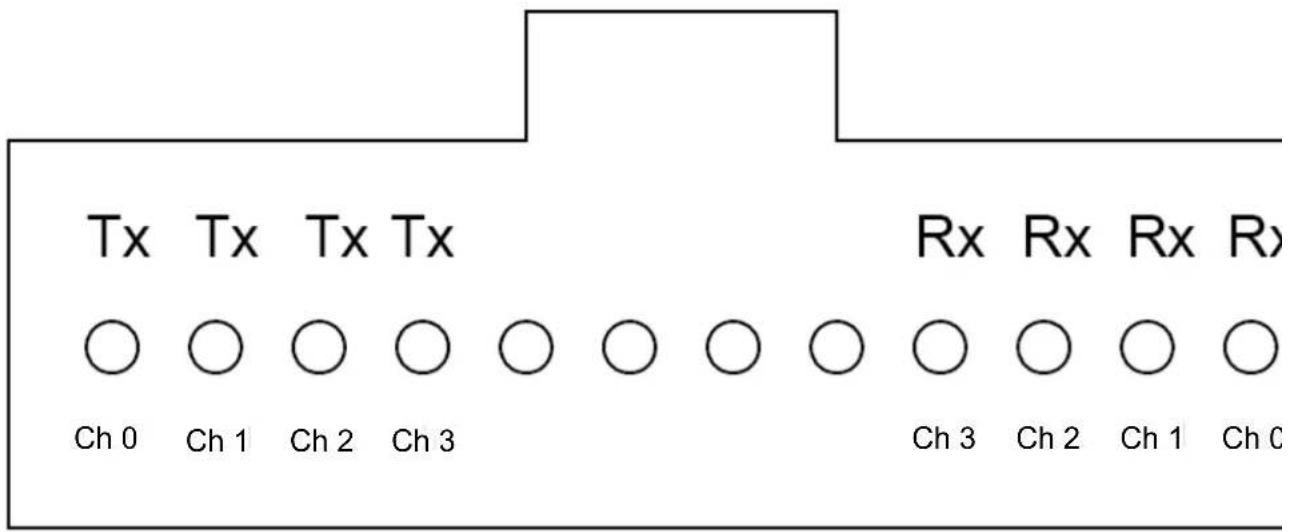
Figure 4 – FTL410QE3C optical lane assignment (front view of MPO receptacle)
X. References
- SFF-8436 – Specification for QSFP+ 10 Gbs 4x Pluggable Transceiver, Rev 4.8, October 2013.
- SFF-8636 – Specification for Common Management Interface, Rev 2.4, November 2014.
- IEEE 802.3ba – PMD Type 40GBASE-SR4.
- Directive 2011/65/EU of the European Council Parliament and of the Council, “on the restriction of the use of certain hazardous substances in electrical and electronic equipment”. Certain products may use one or more exemptions as allowed by the Directive.
- “Application Note AN-2038: Finisar Implementation of RoHS Compliant Transceivers”.
- “Application Note AN-2119: QSFP+ 3 ^rd Generation SR4 Transceiver – EEPROM Mapping”, Rev. B, Finisar Corporation, January, 2015.
XI. For More Information
Finisar Corporation
1389 Moffett Park Drive
Sunnyvale, CA 94089-1133
Tel. 1-408-548-1000
Fax 1-408-541-6138
sales@finisar.com
www.finisar.com