FTL4P1QL1C - Unspecified Finisar - Free user manual and instructions
Find the device manual for free FTL4P1QL1C Finisar in PDF.

User questions about FTL4P1QL1C Finisar
0 question about this device. Answer the ones you know or ask your own.
Ask a new question about this device
Download the instructions for your Unspecified in PDF format for free! Find your manual FTL4P1QL1C - Finisar and take your electronic device back in hand. On this page are published all the documents necessary for the use of your device. FTL4P1QL1C by Finisar.
USER MANUAL FTL4P1QL1C Finisar
PRELIMINARY Product Specification
4x10GBASE-LR Lite QSFP+ Optical Transceiver Module
FTL4P1QL1C
PRODUCT FEATURES
• Hot-pluggable QSFP+ form factor
• Supports 4 independent streams of 10GBASE-LR Lite
• Power dissipation < 2.5W
- RoHS-6 compliant
• Commercial case temperature range 0°C to 70°C
- Single 3.3V power supply
• Maximum link length of 2km and 4 dB insertion loss on single mode fiber (SMF)
- XLPPI electrical interface
- MPO12 receptacle
• Built-in digital diagnostic functions, including Tx/Rx power monitoring

natural_image
3D CAD model of a mechanical component with blue handle and gray casing (no text or symbols)APPLICATIONS
• 10GBASE-LR Lite 10G Ethernet
Finisar's FTL4P1QE1C QSFP+ transceiver modules are designed for use in high density 10 Gigabit Ethernet links over single mode fiber. They are compliant with the QSFP+ MSA ^1,2 and a Lite version of IEEE 802.3ae 10GBASE-LR/LW ^3 . Digital diagnostics functions are available via an I2C interface, as specified by the QSFP+ MSA. The transceiver is RoHS compliant per Directive 2011/65/EU ^4 and Finisar Application Note AN-2038 ^5 .
PRODUCT SELECTION
FTL4P1QL1C
4: 4 channel module
P1: Parallel single mode
Q: QSFP+ form factor
L: 10GBASE-LR Lite optical interface
1: First generation product
C: Commercial temperature range
I. Pin Descriptions
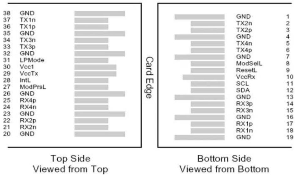
Figure 1 - QSFP+ MSA-compliant 38-pin connector
| Pin | Symbol | Name/Description | Notes |
| 1 | GND | Ground | 1 |
| 2 | Tx2n | Transmitter Inverted Data Input | |
| 3 | Tx2p | Transmitter Non-Inverted Data Input | |
| 4 | GND | Ground | 1 |
| 5 | Tx4n | Transmitter Inverted Data Input | |
| 6 | Tx4p | Transmitter Non-Inverted Data Input | |
| 7 | GND | Ground | 1 |
| 8 | ModSelL | Module Select | |
| 9 | ResetL | Module Reset | |
| 10 | Vcc Rx | +3.3 V Power supply receiver | |
| 11 | SCL | 2-wire serial interface clock | |
| 12 | SDA | 2-wire serial interface data | |
| 13 | GND | Ground | 1 |
| 14 | Rx3p | Receiver Non-Inverted Data Output | |
| 15 | Rx3n | Receiver Inverted Data Output | |
| 16 | GND | Ground | 1 |
| 17 | Rx1p | Receiver Non-Inverted Data Output | |
| 18 | Rx1n | Receiver Inverted Data Output | |
| 19 | GND | Ground | 1 |
| 20 | GND | Ground | 1 |
| 21 | Rx2n | Receiver Inverted Data Output | |
| 22 | Rx2p | Receiver Non-Inverted Data Output | |
| 23 | GND | Ground | 1 |
| 24 | Rx4n | Receiver Inverted Data Output | |
| 25 | Rx4p | Receiver Non-Inverted Data Output | |
| 26 | GND | Ground | 1 |
| 27 | ModPrsL | Module Present | |
| 28 | IntL | Interrupt | |
| 29 | Vcc Tx | +3.3 V Power supply transmitter | |
| 30 | Vcc1 | +3.3 V Power Supply | |
| 31 | LPMode | Low Power Mode | |
| 32 | GND | Ground | 1 |
| 33 | Tx3p | Transmitter Non-Inverted Data Input | |
| 34 | Tx3n | Transmitter Inverted Data Input | |
| 35 | GND | Ground | 1 |
| 36 | Tx1p | Transmitter Non-Inverted Data Input | |
| 37 | Tx1n | Transmitter Inverted Data Input | |
| 38 | GND | Ground | 1 |
Notes
- Circuit ground is internally isolated from chassis ground.
II. General Product Characteristics
| Parameter | Value | Unit | Notes |
| Module Form Factor | QSFP+ | ||
| Maximum Aggregate Data Rate | 41.2 | Gb/s | |
| Maximum Data Rate per Lane | 10.3125 | Gb/s | |
| Protocols Supported | 10G Ethernet | ||
| Electrical Interface and Pin-out | 38-pin edge connector | Pin-out as defined by the QSFP+ MSA | |
| Maximum Power Consumption | 2.5 | Watts | |
| Management Interface | Serial, I2C-based, 400 kHz maximum frequency | As defined by the QSFP+ MSA |
| Data Rate Specifications | Symbol | Min | Typ | Max | Units | Ref. |
| Bit Rate per Lane | BR | 9.95 | 10.313 | Gb/sec | ||
| Bit Error Ratio | BER | 10^-12 | 1 | |||
| Link distance on SMF-28 | d | 2 | kilometers | 2 | ||
| Link insertion loss on SMF-28 | 4.0 | dB | 2 |
Notes:
- Tested with a PRBS 2 ^31 -1 test pattern.
- 10GBASE-LR Lite.
III. Absolute Maximum Ratings
| Parameter | Symbol | Min | Typ | Max | Unit | Ref. |
| Maximum Supply Voltage | Vcc1, VccTx, VccRx | -0.5 | 3.6 | V | ||
| Storage Temperature | T_S | -40 | 85 | °C | ||
| Case Operating Temperature | T_OP | 0 | 70 | °C | ||
| Relative Humidity | RH | 0 | 85 | % | 1 | |
| Damage Threshold, per Lane | DT | 3.4 | dBm |
Notes:
1. Non-condensing.
IV. Electrical Characteristics (T OP = 0 to 70°C, V CC = 3.1 to 3.47 Volts)
| Parameter | Symbol | Min | Typ | Max | Unit | Ref. |
| Supply Voltage | Vcc1, VccTx, VccRx | 3.1 | 3.47 | V | ||
| Supply Current | Icc | ???? | A | |||
| Link turn-on time | ||||||
| Transmit turn-on time | 2000 | ms | 2 | |||
| Transmitter (per Lane) | ||||||
| Single ended input voltage tolerance | VinT | -0.3 | 4.0 | V | ||
| Differential data input swing | Vin,pp | 120 | 1200 | mVpp | 3 | |
| Differential input threshold | 50 | mV | ||||
| AC common mode input voltage tolerance (RMS) | 15 | mV | ||||
| Differential input return loss | Per IEEE P802.3ba, Section 86A.4.1.1 | dB | 4 | |||
| J2 Jitter Tolerance | Jt2 | 0.17 | UI | |||
| J9 Jitter Tolerance | Jt9 | 0.29 | UI | |||
| Data Dependent Pulse Width Shrinkage | DDPWS | 0.07 | UI | |||
| Eye mask coordinates {X1, X2 Y1, Y2} | 0.11, 0.31 95, 350 | UI mV | 5 | |||
| Receiver (per Lane) | ||||||
| Single-ended output voltage | -0.3 | 4.0 | V | |||
| Differential data output swing | Vout,pp | 200 | 400 | mVpp | 6.7 | |
| 300 | 600 | |||||
| 400 | 800 | |||||
| 600 | 1200 | |||||
| AC common mode output voltage (RMS) | 7.5 | mV | ||||
| Termination mismatch at 1 MHz | 5 | % | ||||
| Differential output return loss | Per IEEE P802.3ba, Section 86A.4.2.1 | dB | 4 | |||
| Common mode output return loss | Per IEEE P802.3ba, Section 86A.4.2.2 | dB | 4 | |||
| Output transition time, 20% to 80% | 28 | ps | ||||
| J2 Jitter output | Jo2 | 0.42 | UI | |||
| J9 Jitter output | Jo9 | 0.65 | UI | |||
| Eye mask coordinates #1 {X1, X2Y1, Y2} | 0.29, 0.5150, 425 | UImV | 5 | |||
| Power Supply Ripple Tolerance | PSR | 50 | mVpp | |||
Notes:
1. Maximum total power value is specified across the full temperature and voltage range.
2. From power-on and end of any fault conditions.
3. After internal AC coupling. Self-biasing 100Ω differential input.
4. 10 MHz to 11.1 GHz range.
5. Hit ratio = 5 x 10E-5.
6. AC coupled with 100 differential output impedance.
7. Output voltage settable in four discrete ranges via I2C command.
V. Optical Characteristics (T OP = 0 to 70^ , V_CC = 3.1 to 3.47 Volts)
| Parameter | Symbol | Min | Typ | Max | Unit | Ref. |
| Transmitter | ||||||
| Signaling Speed per Lane | 9.95 | 10.3125 | GBd | 1 | ||
| Lane center wavelength | 1260 | 1355 | ||||
| Total Average Launch Power | P_OUT | 6.5 | dBm | |||
| Transmit OMA per Lane | TxOMA | -6.4 | 3.0 | dBm | ||
| Transmitter and Dispersion Penalty | TDP | 6.4 | dB | |||
| Transmit OMA - TDP | Tp-OMA | -8.4 | dBm | |||
| Average Launch Power per Lane | TXP_x | -9.4 | 0.5 | dBm | 2 | |
| Optical Extinction Ratio | ER | 3.5 | dB | |||
| Sidemode Suppression ratio | SSR_min | 30 | dB | |||
| Average launch power of OFF transmitter, per lane | -30 | dBm | ||||
| Relative Intensity Noise | RIN | -128 | dB/Hz | 3 | ||
| Tx Jitter | Tx_i | 20 | dB | |||
| Transmitter Reflectance | Per 802.3ae requirements | |||||
| Transmitter eye mask definition | Per 802.3ae requirements | |||||
| Receiver | ||||||
| Signaling Speed per Lane | 9.95 | 10.3125 | GBd | 4 | ||
| Lane center wavelength | 1260 | 1355 | ||||
| Average Receive Power per Lane | RXP_x | -14.4 | 0.5 | dBm | 5 | |
| Receiver Sensitivity (OMA) per Lane | Rxsens | -12.6 | dBm | |||
| Stressed Receiver Sensitivity (OMA) per Lane | SRS | -10.3 | dBm | |||
| Damage Threshold per Lane | P_MAX | 3.5 | dBm | |||
| Return Loss | R_L | -12 | dB | |||
| Receive electrical 3 dB upper cutoff frequency, per lane | 12.3 | GHz | ||||
| LOS De-Assert | LOS_D | -17 | dBm | |||
| LOS Assert | LOS_A | -30 | dBm | |||
| LOS Hysteresis | 0.5 | dB | ||||
| Link Power Budget | ||||||
| Power Budget | 6.2 | dB | ||||
| Link Insertion Loss | 4.0 | dB | 6 | |||
Notes:
- Transmitter consists of 4 lasers operating at 9.95 or 10.3Gb/s each.
- Minimum value is informative.
- RIN is scaled by 10*(10/4) to maintain SNR outside of transmitter.
- Receiver consists of 4 photodetectors operating at 9.95 or 10.3Gb/s each.
- Minimum value is informative, equals min TxOMA with infinite ER and max channel insertion loss.
- Insertion loss includes 0.8 dB for fiber attenuation and 3.2 dB for connector and splice loss.
VI. Digital Diagnostic Specifications
FTL4P1QL1C transceivers can be used in host systems that require either internally or externally calibrated digital diagnostics.
| Parameter | Symbol | Min | Typ | Max | Units | Ref. |
| Accuracy | ||||||
| Internally measured transceiver temperature | DD_Temperature | 3 | °C | |||
| Internally measured transceiver supply voltage | DD_Voltage | 3 | % | |||
| Measured TX bias current | DD_Bias | 10 | % | 1 | ||
| Measured TX output power | DD_Tx-Power | 2 | dB | |||
| Measured RX received average optical power | DD_Rx-Power | 2 | dB | |||
| Dynamic Range for Rated Accuracy | ||||||
| Internally measured transceiver temperature | DD_Temperature | -5 | 70 | °C | ||
| Internally measured transceiver supply voltage | DD_Voltage | 3.1 | 3.5 | V | ||
| Measured TX bias current | DD_Bias | 10 | 90 | mA | ||
| Measured TX output power | DD_Tx-Power | -8.2 | +0.5 | dBm | ||
| Measured RX received average optical power | DD_Rx-Power | -14.2 | +0.5 | dBm | ||
| Max Reporting Range | ||||||
| Internally measured transceiver temperature | DD_Temperature | -40 | 125 | °C | ||
| Internally measured transceiver supply voltage | DD_Voltage | 2.8 | 4.0 | V | ||
| Measured TX bias current | DD_Bias | 0 | 20 | mA | ||
| Measured TX output power | DD_Tx-Power | -10 | +2 | dBm | ||
| Measured RX received average optical power | DD_Rx-Power | -22 | +2 | dBm | ||
Notes:
- Accuracy of measured Tx bias current is 10% of the actual bias current from the laser driver to the laser.
VII. Memory Map and Control Registers
Compatible with SFF-8436 (QSFP+). Please see Finisar Application Note AN-2104 ^4 .
VIII. Environmental Specifications
Finisar FTL4P1QL1C transceivers have an operating temperature range from 0°C to +70°C case temperature.
| Environmental Specifications | Symbol | Min | Typ | Max | Units | Ref. |
| Case Operating Temperature | T_op | 0 | 70 | °C | ||
| Storage Temperature | T_sto | -40 | 85 | °C |
IX. Regulatory Compliance
Finisar FTL4P1QL1C transceivers are RoHS-6 Compliant. Copies of certificates are available at Finisar Corporation upon request.
FTL4P1QL1C transceiver modules are Class 1 laser eye safety compliant per IEC 60825-1.
X. Mechanical Specifications
The FTL4P1QL1C mechanical specifications are compliant to the QSFP+ MSA transceiver module specifications.
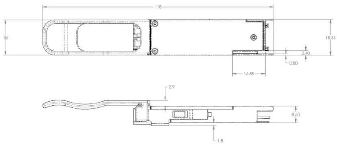
Figure 2 - FTL4P1QL1C mechanical drawing
The FTL4P1QM1C pull tab color is dark blue Pantone 2748.
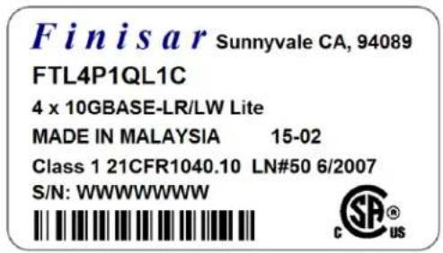
Figure 3 - FTL4P1QL1C label (not to scale)
The FTL4P1QL1C optical interface accepts an 8^ angled MPO connector, with lane assignments as shown in Figure 4.
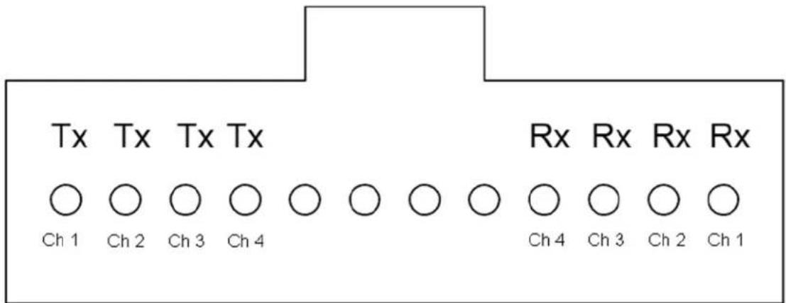
Figure 4 - FTL4P1QL1C optical lane assignment (front view of MPO receptacle)
XI. References
- SFF-8436 – Specification for QSFP+ 10 Gbs 4x Pluggable Transceiver, Rev 4.8, October 2013.
- SFF-8636 – Specification for Common Management Interface, Rev 1.7, January 2014.
- 802.3-2012, IEEE Standard for Ethernet, Section 4, Clause 52, PMD Types 10GBASE-LR/LW.
- Directive 2011/65/EU of the European Council Parliament and of the Council, “on the restriction of the use of certain hazardous substances in electrical and electronic equipment,” June 8, 2011, which supercedes the previous RoHS Directive 2002/95/EC.
- “Application Note AN-2038: Finisar Implementation of RoHS Compliant Transceivers”, Finisar Corporation, January 21, 2005.
- “Application Note AN-2104: QSFP+ 40G LR4 Transceiver EEPROM Mapping,” Rev. A, Finisar Corporation, June, 2013.
XII. For More Information
Finisar Corporation
1389 Moffett Park Drive
Sunnyvale, CA 94089-1133
Tel. 1-408-548-1000
Fax 1-408-541-6138
.sales@finisar.com
.www.finisar.com