FTLF1429P3BCE - Network adapter Finisar - Free user manual and instructions
Find the device manual for free FTLF1429P3BCE Finisar in PDF.

User questions about FTLF1429P3BCE Finisar
0 question about this device. Answer the ones you know or ask your own.
Ask a new question about this device
Download the instructions for your Network adapter in PDF format for free! Find your manual FTLF1429P3BCE - Finisar and take your electronic device back in hand. On this page are published all the documents necessary for the use of your device. FTLF1429P3BCE by Finisar.
USER MANUAL FTLF1429P3BCE Finisar
Product Specification
16GFC RoHS Compliant Long-Wavelength SFP+ Transceiver
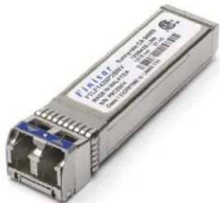
FTLF1429P3BCE
PRODUCT FEATURES
- Up to 14.025 Gb/s bi-directional data links
• Hot-pluggable SFP+ footprint
• Built-in digital diagnostic functions
• 1310nm DFB laser transmitter - Duplex LC connector
• RoHS compliant and Lead Free
• Up to 25 km on 9/125μm SMF
• Metal enclosure, for lower EMI - 1W maximum power consumption with established link
• Single 3.3V power supply - Extended operating temperature range: 0°C to 70°C
APPLICATIONS
• Tri Rate 4.25 / 8.5 / 14.025 Gb/s Fibre Channel through Rate Select
Finisar's FTLF1429P3BNV SFP+ transceivers are designed for use in Fibre Channel links up to 14.025 Gb/s data rate and up to 25 km link length. They are compliant with FC-PI-5 Rev. 6.10^1 and SFF-8472 Rev 11.0^3 , and compatible with SFF- 8432^2 and applicable portions of SFF-8431 Rev. 3.0^4 . The optical transceiver is compliant per the RoHS Directive 2011/65/EU ^5 . See Finisar Application Note AN-2038 for more details ^6 .
PRODUCT SELECTION
FTLF1429P3BCE
I. Pin Descriptions
| Pin | Symbol | Name/Description | Ref. |
| 1 | V_EET | Transmitter Ground (Common with Receiver Ground) | 1 |
| 2 | T_FAULT | Transmitter Fault. | 2 |
| 3 | T_DIS | Transmitter Disable. Laser output disabled on high or open. | 3 |
| 4 | SDA | 2-wire Serial Interface Data Line (MOD-DEF2) | 4 |
| 5 | SCA | 2-wire Serial Interface Clock (MOD-DEF1) | 4 |
| 6 | MOD_ABS | Module Absent, connected to V_EET or V_EER | 4 |
| 7 | RS0 | Rx Rate Select:Open or Low = 4.25 or 8.5 Gb/s Fibre Channel (Low Bandwidth)High = 14.025 Gb/s Fibre Channel (High Bandwidth) | 5 |
| 8 | LOS | Loss of Signal indication. Logic 0 indicates normal operation. | 6 |
| 9 | RS1 | Tx Rate Select:Open or Low = 4.25 or 8.5 Gb/s Fibre Channel (Low Bandwidth)High = 14.025 Gb/s Fibre Channel (High Bandwidth) | 5 |
| 10 | V_EER | Receiver Ground (Common with Transmitter Ground) | 1 |
| 11 | V_EER | Receiver Ground (Common with Transmitter Ground) | 1 |
| 12 | RD- | Receiver Inverted DATA out. AC Coupled | |
| 13 | RD+ | Receiver Non-inverted DATA out. AC Coupled | |
| 14 | V_EER | Receiver Ground (Common with Transmitter Ground) | 1 |
| 15 | V_CCR | Receiver Power Supply | |
| 16 | V_CCT | Transmitter Power Supply | |
| 17 | V_EET | Transmitter Ground (Common with Receiver Ground) | 1 |
| 18 | TD+ | Transmitter Non-Inverted DATA in. AC Coupled. | |
| 19 | TD- | Transmitter Inverted DATA in. AC Coupled. | |
| 20 | V_EET | Transmitter Ground (Common with Receiver Ground) | 1 |
Notes:
- Circuit ground is internally isolated from chassis ground.
- T_FAULT is an open collector/drain output, which should be pulled up with a 4.7k – 10k Ohms resistor on the host board if intended for use. Pull up voltage should be between 2.0V to Vcc + 0.3V. A high output indicates a transmitter fault caused by either the TX bias current or the TX output power exceeding the preset alarm thresholds. A low output indicates normal operation. In the low state, the output is pulled to <0.8V.
- Laser output disabled on T_DIS >2.0V or open, enabled on T_DIS <0.8V .
- Should be pulled up with 4.7k – 10kohms on host board to a voltage between 2.0V and 3.6V. MOD_ABS pulls line low to indicate module is plugged in.
- Rate select can also be set through the 2-wire bus in accordance with SFF-8472 v. 10.2. Rx Rate Select is set at Bit 3, Byte 110, Address A2h. Tx Rate Select is set at Bit 3, Byte 118, Address A2h. Note: writing a "1" selects maximum bandwidth operation. Rate select is the logic OR of the input state of Rate Select Pin and 2-wire bus.
- LOS is open collector output. Should be pulled up with 4.7k – 10kohms on host board to a voltage between 2.0V and 3.6V. Logic 0 indicates normal operation; logic 1 indicates loss of signal.
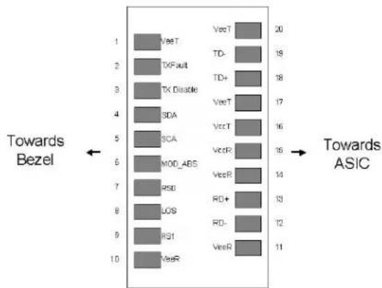
Pinout of Connector Block on Host Board
II. Absolute Maximum Ratings
| Parameter | Symbol | Min | Typ | Max | Unit | Ref. |
| Maximum Supply Voltage | Vcc | -0.5 | 4.2 | V | ||
| Storage Temperature | T_S | -40 | 85 | °C | ||
| Case Operating Temperature | T_OP | 0 | 70 | °C | ||
| Relative Humidity | RH | 0 | 85 | % | 1 |
III. Electrical Characteristics ( T_OP = 0 to 70 °C, V_CC = 3.00 to 3.60 Volts)
| Parameter | Symbol | Min | Typ | Max | Unit | Ref. |
| Supply Voltage | Vcc | 3.15 | 3.45 | V | 2 | |
| Supply Current | Icc | 200 | 300 | mA | 2 | |
| Transmitter | ||||||
| Input differential impedance | R_in | 100 | Ω | 3 | ||
| Single ended data input swing | Vin,pp | 90 | 350 | mV | ||
| Transmit Disable Voltage | V_D | 2 | VccT+0.3 | V | ||
| Transmit Enable Voltage | V_EN | Vee | Vcc+ 0.8 | V | 4 | |
| Receiver | ||||||
| Single ended data output swing | Vout,pp | 185 | 425 | mV | 5 | |
| Data output rise/fall time, 4.25 Gb/s | t_r,t_f | 120 | ps | 6 | ||
| LOS Fault | V_LOS fault | 2 | Vcc_HOST | V | 7 | |
| LOS Normal | V_LOS norm | Vee-0.3 | Vee+0.4 | V | 7 | |
| Power Supply Rejection | PSR | 66 | mVpp | 8 | ||
Notes:
- Non-condensing.
- Module power consumption never exceeds 1W with established link.
- AC coupled.
- Or open circuit.
- Into 100 ohm differential termination.
-
20 - 80 %.
-
LOS is LVTTL. Logic 0 indicates normal operation; logic 1 indicates no signal detected.
-
All transceiver specifications are compliant with a power supply sinusoidal modulation of 20Hz to 1.5 MHz up to specified value applied through the power supply filtering network shown on page 23 of the
Small Form-factor Pluggable (SFP) Transceiver MultiSource Agreement (MSA) ^6 , September 14, 2000. The Power Supply Rejection applies for a supply voltage range of 3.1 to 3.6 V.
- Measured with DJ-free data input signal. In actual application, output DJ will be the sum of input DJ and DJ.
- For 14.025 and 8.5 Gb/s operation, Deterministic Jitter and Total Jitter are not specified per FC-PI-5 Rev 6.10. Jitter values for gamma T and gamma R are controlled by TDP and stressed receiver sensitivity.
IV. Optical Characteristics (T OP = 0 to 70^ , V_CC = 3.15 to 3.45 Volts)
| Parameter | Symbol | Min | Typ | Max | Unit | Ref. |
| Transmitter | ||||||
| Output Opt. Power | P_O | -2.0 | +6.0 | dBm | 1 | |
| Optical Wavelength | λ | 1295 | 1325 | nm | ||
| Spectral Width | σ | 1 | nm | 2 | ||
| Optical Modulation Amplitude | OMA | 1260 | μW | 3 | ||
| Transmitter and Dispersion Penalty, 14.025 Gb/s | TDP | 4.4 | dB | 4 | ||
| Transmitter and Dispersion Penalty, 8.5 Gb/s | TDP | 3.2 | dB | 4 | ||
| Optical Rise/Fall Time, 4.25 Gb/s | t_r/t_f | 90 | ps | 5 | ||
| RIN | -130 | dB/Hz | ||||
| Receiver | ||||||
| Unstressed Receiver OMA Sensitivity, 14.025 Gb/s | R_SENSr | 0.039 | mW | 6 | ||
| Unstressed Receiver OMA Sensitivity, 8.5 Gb/s | R_SENSr | 0.039 | mW | 7 | ||
| Unstressed Receiver OMA Sensitivity, 4.25 Gb/s | R_SENS4 | 0.029 | mW | 7 | ||
| Average Received Power | Rx_MAX | +3.0 | dBm | |||
| Optical Center Wavelength | _C | 1260 | 1370 | nm | ||
| Return Loss | 12 | dB | ||||
| LOS De-Assert | LOS_D | -19 | dBm | |||
| LOS Assert | LOS_A | -30 | dBm | |||
| LOS Hysteresis | 0.5 | dB | ||||
| Parameter | Symbol | Min | Typ | Max | Unit | Ref. |
Notes:
- Class 1 Laser Safety per FDA/CDRH and EN (IEC) 60825 regulations.
- 20dB spectral width.
- Equivalent extinction ratio specification for Fibre Channel. Allows smaller ER at higher average power.
- For 14.025 and 8.5 Gb/s operation, Jitter values for gamma T and gamma R are controlled by TDP.
- Unfiltered, 20-80%. Complies with IEEE 802.3 (Gig. E), FC 4x eye masks when filtered.
- High Bandwidth Mode. Measured with PRBS 2 ^31 -1 at 10 ^-12 BER.
- Low Bandwidth Mode. Measured with PRBS 2 ^7 -1 at 10-12 BER.
V. General Specifications
| Parameter | Symbol | Min | Typ | Max | Units | Ref. |
| Data Rate | BR | 4.25 | 14.025 | Gb/sec | 1 | |
| Bit Error Rate | BER | 10^-12 | 2 | |||
| Supported Link Length on 9/125 μm SMF, 4.25, 8.5, 14.025 Gb/s | L_MAX | 25 | km | 3 |
Notes:
- 4x/8x/16x Fibre Channel compliant.
- Tested with a PRBS 2 ^7 -1 test pattern for 4.25 and 8.5Gb/s operation. Tested with a PRBS 2 ^31 -1 test pattern for 14.025Gb/s operation.
- Based on 15dB link budget.
VI. Environmental Specifications
These Finisar 1310nm Commercial Temperature SFP+ transceivers have an operating temperature range from 0^ C to +70^ C case temperature.
| Parameter | Symbol | Min | Typ | Max | Units | Ref. |
| Case Operating Temperature | T_op | 0 | 70 | °C | ||
| Storage Temperature | T_sto | -40 | 85 | °C |
VII. Regulatory Compliance
Finisar transceivers are Class 1 Laser Products and comply with US FDA regulations. These products are certified by TÜV and CSA to meet the Class 1 eye safety requirements of EN (IEC) 60825 and the electrical safety requirements of EN (IEC) 60950. Copies of certificates are available at Finisar Corporation upon request.
VIII. Digital Diagnostic Functions
Finisar FTLF1429P3BNV SFP+ transceivers support the 2-wire serial communication protocol as defined in the SFP MSA ^6 . It is very closely related to the E ^2 PROM defined in the GBIC standard, with the same electrical specifications.
The standard SFP serial ID provides access to identification information that describes the transceiver's capabilities, standard interfaces, manufacturer, and other information.
Additionally, Finisar SFP transceivers provide a unique enhanced digital diagnostic monitoring interface, which allows real-time access to device operating parameters such as transceiver temperature, laser bias current, transmitted optical power, received optical power and transceiver supply voltage. It also defines a sophisticated system of alarm and warning flags, which alerts end-users when particular operating parameters are outside of a factory set normal range.
The SFP MSA defines a 256-byte memory map in E ^2 PROM that is accessible over a 2-wire serial interface at the 8 bit address 1010000X (A0h). The digital diagnostic monitoring interface makes use of the 8 bit address 1010001X (A2h), so the originally defined serial ID memory map remains unchanged. The interface is identical to, and is thus fully backward compatible with both the GBIC Specification and the SFP Multi Source Agreement. The complete interface is described in Finisar Application Note AN-2030: “Digital Diagnostics Monitoring Interface for SFP Optical Transceivers”.
The operating and diagnostics information is monitored and reported by a Digital Diagnostics Transceiver Controller (DDTC) inside the transceiver, which is accessed through a 2-wire serial interface. When the serial protocol is activated, the serial clock signal (SCL, Mod Def 1) is generated by the host. The positive edge clocks data into the SFP transceiver into those segments of the E²PROM that are not write-protected. The negative edge clocks data from the SFP transceiver. The serial data signal (SDA, Mod Def 2) is bi-directional for serial data transfer. The host uses SDA in conjunction with SCL to mark the start and end of serial protocol activation. The memories are organized as a series of 8-bit data words that can be addressed individually or sequentially.
For more information, please see the SFP MSA documentation ^3,6 or Finisar Application Note AN-2030.
FTLF1429P3BNV transceivers can be used in host systems that require either internally or externally calibrated digital diagnostics.
Please note that evaluation board FDB-1027 is available with Finisar ModDEMO software that allows simple to use communication over the 2-wire serial interface.
IX. Mechanical Specifications
Finisar's FTLF1429P3BCE SFP+ transceivers are compatible with the SFF-8432 ^2 specification for improved pluggable form factor.
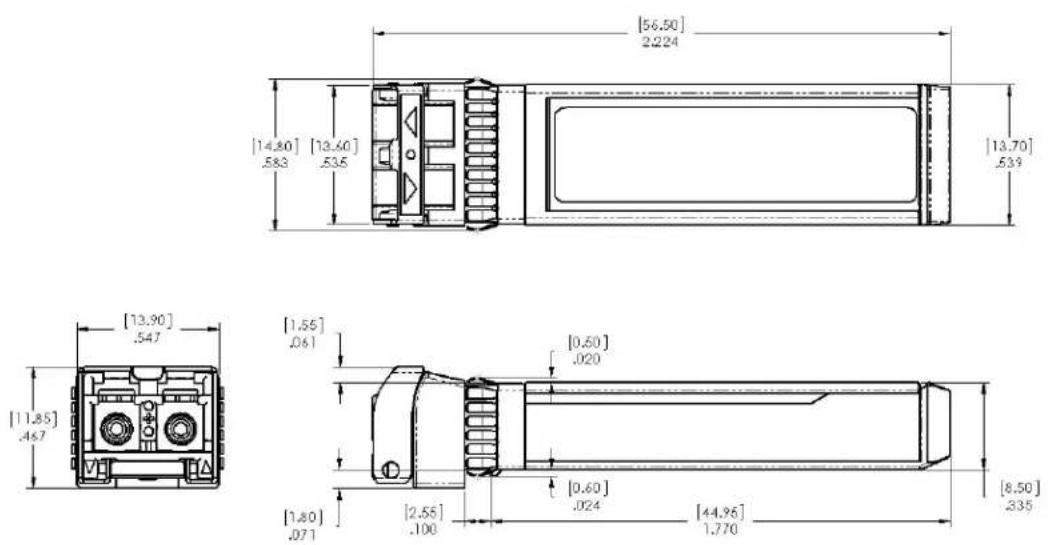
FTLF1429P3BCE
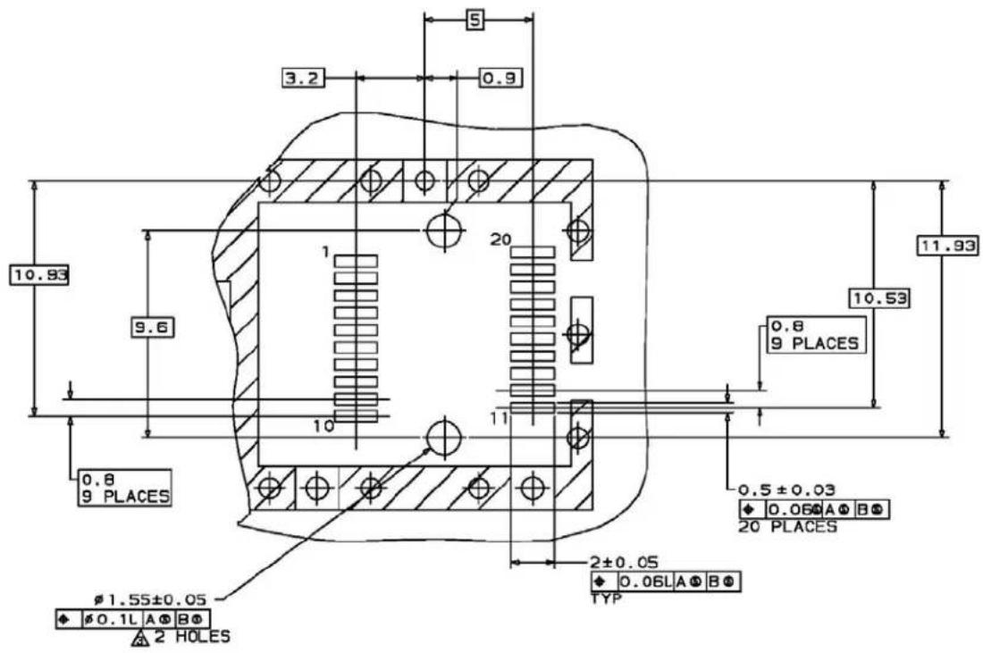
X. PCB Layout and Bezel Recommendations
3 Through Holes are Unpaired
4/3 and Vias are Chassis Group, 11 Places
5/2 and Basic Dimension Established by Customer
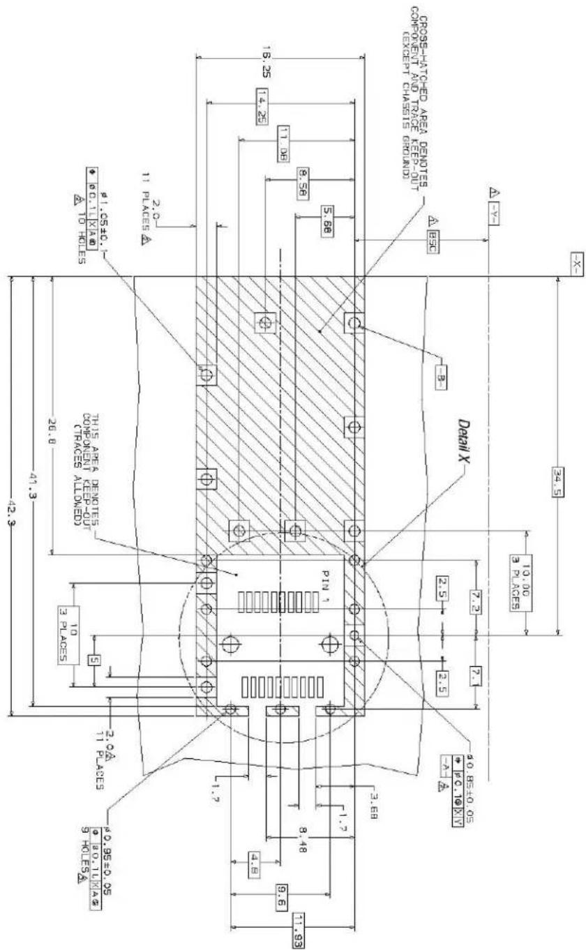
![16.25±0.1 [ .640° ] Y 15.25±0.1 [ .600° ]](/content/2026/06/1189077/images/1a656fb114e5c8a7b75ad172bf11552396b88a62395303192518a3dc2f7ef016.jpg)
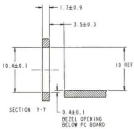
NOTES:
△ MINIMUM PITCH ILLUSTRATED, ENGLISH DIMENSIONS ARE FOR REFERENCE ONLY
2. NOT RECOMMENDED FOR PCI EXPANSION CARD APPLICATIONS
XI. References
- “Fibre Channel Physical Interface-5 Specification (FC-PI-5 Rev. 6.10)”. American National Standard for Information Technology, January 11, 2011.
- “Improved Pluggable Formfactor”, SFF Document Number SFF-8432, Revision 5.0, July 16, 2007.
- “Digital Monitoring Interface for Optical Transceivers”, SFF Document Number SFF-8472, Revision 11.0, September 14, 2000.
- “Enhanced Specification for 8.5 and 10 Gigabit Small Form Factor Pluggable Module ‘SFP+ ‘”, SFF Document Number SFF-8431, Revision 3.0, May 8, 2008.
- Directive 2011/65/EU of the European Council Parliament and of the Council, "on the restriction of the use of certain hazardous substances in electrical and electronic equipment". Certain products may use one or more exemptions as allowed by the Directive.
- “Application Note AN-2038: Finisar Implementation of RoHS Compliant Transceivers”.
- Small Form Factor Pluggable (SFP) Transceiver Multi-source Agreement (MSA), September 14, 2000.
XII. For More Information
Finisar Corporation
1389 Moffett Park Drive
Sunnyvale, CA 94089-1134
Tel. 1-408-548-1000
Fax 1-408-541-6138
sales@finisar.com
www.finisar.com