FTLD10CE3C - Composant optique Finisar - Free user manual and instructions
Find the device manual for free FTLD10CE3C Finisar in PDF.

User questions about FTLD10CE3C Finisar
0 question about this device. Answer the ones you know or ask your own.
Ask a new question about this device
Download the instructions for your Composant optique in PDF format for free! Find your manual FTLD10CE3C - Finisar and take your electronic device back in hand. On this page are published all the documents necessary for the use of your device. FTLD10CE3C by Finisar.
USER MANUAL FTLD10CE3C Finisar
Product Specification
100GBASE-SR10 100m CXP Optical Transceiver Module
FTLD10CE3C
PRODUCT FEATURES
• 12-channel full-duplex transceiver module
• Hot Pluggable CXP form factor
- Multirate capability: 1Gb/s to 11.3Gb/s per channel
• Maximum link length of 100m on OM3 Multimode Fiber (MMF)
- Unretimed CPPI electrical interface
- Requires 3.3V power supply only
- Low power dissipation: < 3.5W
• Reliable VCSEL array technology
• Digital Diagnostics including Tx and Rx optical power monitoring
• Commercial operating case temperature range: 0°C to 70°C
• RoHS-6 Compliant (lead-free)
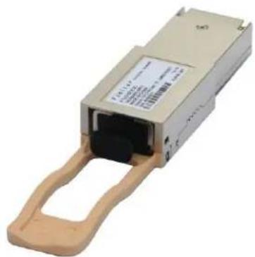
natural_image
Exterior view of a beige electronic device with a black connector and beige handle (no visible text or symbols)APPLICATIONS
• Infiniband 12x SDR/DDR/QDR
• 100GBASE-SR10 100G Ethernet
- OTU4/OTU2e
- 12x 10GBASE-SR Ethernet (compatible)
- PCIe (Gen1/2/3)
- SATA3
- Proprietary protocols
Finisar's FTLD10CE3C second-generation CXP transceiver modules are designed for use in up to 136 Gigabit per second links over 12 duplex multimode fiber pairs. They are compliant with the IBTA CXP Specification ^1 , IEEE 802.3ba 100GBASE-SR10 and CPPI electrical interfaces ^2 . The transceiver is RoHS-6 compliant and lead-free per Directive 2002/95/EC ^3 , and Finisar Application Note AN-2038 ^4 . They support Tx/Rx optical power monitoring functionality. For applications up to 14 Gb/s per channel please contact Finisar.
PRODUCT SELECTION
FTLD10CE3C
E: Ethernet-compliant optical interface
3: Second generation product
C: Commercial temperature rate
I. Pin Descriptions
| Bottom side | Top Side | |||||
| I/O # | Name | Contact Length | Contact Length | Name | I/O # | |
| Receiver -- Top Card | ||||||
| C1 | GND | 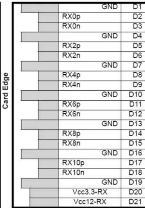 | ||||
| C2 | RX1p | |||||
| C3 | RX1n | |||||
| C4 | GND | |||||
| C5 | RX3p | |||||
| C6 | RX3n | |||||
| C7 | GND | |||||
| C8 | RX5p | |||||
| C9 | RX5n | |||||
| C10 | GND | |||||
| C11 | RX7p | |||||
| C12 | RX7n | |||||
| C13 | GND | |||||
| C14 | RX9p | |||||
| C15 | RX9n | |||||
| C16 | GND | |||||
| C17 | RX11p | |||||
| C18 | RX11n | |||||
| C19 | GND | |||||
| C20 | PRSNT_L | |||||
| C21 | Int_L/Reset_L | |||||
| Transmitter -- Bottom Card | ||||||
| A1 | GND | Card Edge | GND | B1 | ||
| A2 | TX1p | TX0p | B2 | |||
| A3 | TX1n | TX0n | B3 | |||
| A4 | GND | GND | B4 | |||
| A5 | TX3p | TX2p | B5 | |||
| A6 | TX3n | TX2n | B6 | |||
| A7 | GND | GND | B7 | |||
| A8 | TX5p | TX4p | B8 | |||
| A9 | TX5n | TX4n | B9 | |||
| A10 | GND | GND | B10 | |||
| A11 | TX7p | TX6p | B11 | |||
| A12 | TX7n | TX6n | B12 | |||
| A13 | GND | GND | B13 | |||
| A14 | TX9p | TX8p | B14 | |||
| A15 | TX9n | TX8n | B15 | |||
| A16 | GND | GND | B16 | |||
| A17 | TX11p | TX10p | B17 | |||
| A18 | TX11n | TX10n | B18 | |||
| A19 | GND | GND | B19 | |||
| A20 | SCL | VCC3.3-TX | B20 | |||
| A21 | SDA | VCC12-TX | B21 | |||
Transmitter -- Bottom Card
| A1 | GND | ||
| A2 | TX1p | ||
| A3 | TX1n | ||
| A4 | GND | ||
| A5 | TX3p | ||
| A6 | TX3n | ||
| A7 | GND | ||
| A8 | TX5p | ||
| A9 | TX5n | ||
| A10 | GND | ||
| A11 | TX7p | ||
| A12 | TX7n | ||
| A13 | GND | ||
| A14 | TX9p | ||
| A15 | TX9n | ||
| A16 | GND | ||
| A17 | TX11p | ||
| A18 | TX11n | ||
| A19 | GND | ||
| A20 | SCL | ||
| A21 | SDA | ||
Figure 1 - CXP-compliant 84-pin connector
| Pin | Symbol | Name/Description | Notes |
| A1 | GND | Ground | 1 |
| A2 | Tx1p | Transmitter Non-Inverted Data Input | |
| A3 | Tx1n | Transmitter Inverted Data Input | |
| A4 | GND | Ground | 1 |
| A5 | Tx3p | Transmitter Non-Inverted Data Input | |
| A6 | Tx3n | Transmitter Inverted Data Input | |
| A7 | GND | Ground | 1 |
| A8 | Tx5p | Transmitter Non-Inverted Data Input | |
| A9 | Tx5n | Transmitter Inverted Data Input | |
| A10 | GND | Ground | 1 |
| A11 | Tx7p | Transmitter Non-Inverted Data Input | |
| A12 | Tx7n | Transmitter Inverted Data Input | |
| A13 | GND | Ground | 1 |
| A14 | Tx9p | Transmitter Non-Inverted Data Input | |
| A15 | Tx9n | Transmitter Inverted Data Input | |
| A16 | GND | Ground | 1 |
| A17 | Tx11p | Transmitter Non-Inverted Data Input | |
| A18 | Tx11n | Transmitter Inverted Data Input | |
| A19 | GND | Ground | 1 |
| A20 | SCL | 2-wire serial interface clock | |
| A21 | SDA | 2-wire serial interface data | |
| B1 | GND | Ground | 1 |
| B2 | Tx0p | Transmitter Non-Inverted Data Input | |
| B3 | Tx0n | Transmitter Inverted Data Input | |
| B4 | GND | Ground | 1 |
| B5 | Tx2p | Transmitter Non-Inverted Data Input | |
| B6 | Tx2n | Transmitter Inverted Data Input | |
| B7 | GND | Ground | 1 |
| B8 | Tx4p | Transmitter Non-Inverted Data Input | |
| B9 | Tx4n | Transmitter Inverted Data Input | |
| B10 | GND | Ground | 1 |
| B11 | Tx6p | Transmitter Non-Inverted Data Input | |
| B12 | Tx6n | Transmitter Inverted Data Input | |
| B13 | GND | Ground | 1 |
| B14 | Tx8p | Transmitter Non-Inverted Data Input | |
| B15 | Tx8n | Transmitter Inverted Data Input | |
| B16 | GND | Ground | 1 |
| B17 | Tx10p | Transmitter Non-Inverted Data Input | |
| B18 | Tx10n | Transmitter Inverted Data Input | |
| B19 | GND | Ground | 1 |
| B20 | VCC3.3-TX | +3.3 V Power supply transmitter | |
| B21 | VCC12-TX | +12.0 V Power supply transmitter - NOT CONNECTED | 2 |
| C1 | GND | Ground | 1 |
| C2 | Rx1p | Receiver Non-Inverted Data Output | |
| C3 | Rx1n | Receiver Inverted Data Output | |
| C4 | GND | Ground | 1 |
| C5 | Rx3p | Receiver Non-Inverted Data Output | |
| C6 | Rx3n | Receiver Inverted Data Output | |
| C7 | GND | Ground | 1 |
| C8 | Rx5p | Receiver Non-Inverted Data Output | |
| C9 | Rx5n | Receiver Inverted Data Output | |
| C10 | GND | Ground | 1 |
| C11 | Rx7p | Receiver Non-Inverted Data Output | |
| C12 | Rx7n | Receiver Inverted Data Output | |
| C13 | GND | Ground | 1 |
| C14 | Rx9p | Receiver Non-Inverted Data Output | |
| C15 | Rx9n | Receiver Inverted Data Output | |
| C16 | GND | Ground | 1 |
| C17 | Rx11p | Receiver Non-Inverted Data Output | |
| C18 | Rx11n | Receiver Inverted Data Output | |
| C19 | GND | Ground | 1 |
| C20 | PRSNT_L | Module Present | |
| C21 | Int_L/Reset_L | Interrupt / Reset | |
| D1 | GND | Ground | 1 |
| D2 | Rx0p | Receiver Non-Inverted Data Output | |
| D3 | Rx0n | Receiver Inverted Data Output | |
| D4 | GND | Ground | 1 |
| D5 | Rx2p | Receiver Non-Inverted Data Output | |
| D6 | Rx2n | Receiver Inverted Data Output | |
| D7 | GND | Ground | 1 |
| D8 | Rx4p | Receiver Non-Inverted Data Output | |
| D9 | Rx4n | Receiver Inverted Data Output | |
| D10 | GND | Ground | 1 |
| D11 | Rx6p | Receiver Non-Inverted Data Output | |
| D12 | Rx6n | Receiver Inverted Data Output | |
| D13 | GND | Ground | 1 |
| D14 | Rx8p | Receiver Non-Inverted Data Output | |
| D15 | Rx8n | Receiver Inverted Data Output | |
| D16 | GND | Ground | 1 |
| D17 | Rx10p | Receiver Non-Inverted Data Output | |
| D18 | Rx10n | Receiver Inverted Data Output | |
| D19 | GND | Ground | 1 |
| D20 | Vcc3.3-RX | +3.3 V Power supply receiver | |
| D21 | Vcc12-RX | +12.0 V Power supply receiver - NOT CONNECTED | 2 |
Notes
-
Circuit ground is internally isolated from chassis ground.
-
12V power supply not required.
II. General Product Characteristics
| Parameter | Value | Unit | Notes |
| Module Form Factor | CXP | ||
| Number of Lanes | 12 Tx and 12 Rx | ||
| Maximum Aggregate Data Rate | 135.816 | Gb/s | |
| Maximum Data Rate per Lane | 11.318 | Gb/s | |
| Protocols Supported | Typical applications include Infiniband DDR/QDR, 100GBASE-SR10 Ethernet, OTU4, OTU2e, PCIe-Gen1/2/3, 12x10GBASE-SR Ethernet | ||
| Electrical Interface and Pin-out | 84-pin edge connector | Pin-out as defined by the CXP Specification | |
| Optical Cable Type Required | Multimode ribbon 24-fiber cable assembly, MPO connector | ||
| Maximum Power Consumption per End | 3.5 | Watts | Varies with output voltage swing and pre-emphasis settings |
| Management Interface | Serial, I2C-based, 400 kHz maximum frequency | As defined by the CXP Specification |
| Data Rate Specifications | Symbol | Min | Typ | Max | Units | Ref. |
| Bit Rate per Lane | BR | 1000 | 11318 | Mb/sec | 1 | |
| Bit Error Ratio @10.3Gb/s per Lane | BER1 | 10^-12 | 2 | |||
| Bit Error Ratio @11.1Gb/s per Lane | BER2 | 10^6 | 2 | |||
| Bit Error Ratio @11.2Gb/s per Lane | BER3 | 10^6 | 2 | |||
| Bit Error Ratio @11.3Gb/s per Lane | BER4 | 10^8 | 2 | |||
| Link distance on OM3 MMF | D1 | 100 | meters | |||
| Link distance on OM4 MMF | D2 | 150 | meters |
Notes:
1. Infiniband SDR/DDR/QDR, 100GBASE-SR10 100G Ethernet, OTU2e, OTU4, PCIe Gen1/2/3, 12x10GBASE-SR 10G Ethernet.
2. Tested with a PRBS 2 ^31 -1 test pattern.
III. Absolute Maximum Ratings
| Parameter | Symbol | Min | Typ | Max | Unit | Ref. |
| Maximum Supply Voltage | V_cc1 , V_ccTx , V_ccRx | -0.5 | 3.6 | V | ||
| Storage Temperature | T_S | -40 | 85 | °C | ||
| Case Operating Temperature | T_OP | 0 | 70 | °C | ||
| Relative Humidity | RH | 0 | 85 | % | 1 |
Notes:
1. Non-condensing.
IV. Electrical Characteristics (T OP = 0 to 70^,V_CC = 3.3± 5% Volts)
NOTE: The FTLD10CE3C requires that a CPPI-compliant CXP electrical connector be used on the host board in order to guarantee its electrical interface specification. Please check with your connector supplier.
| Parameter | Symbol | Min | Typ | Max | Unit | Ref. |
| Supply Voltage | Vcc1, VccTx, VccRx | 3.15 | 3.45 | V | ||
| Supply Current | Icc | 850 | 1000 | mA | ||
| Module Total Power | P | 3.5 | W | 1,7 | ||
| Link Turn-On Time | ||||||
| Transmit turn-on time | 2000 | ms | 2 | |||
| Transmitter (per Lane) | ||||||
| Single ended input voltage tolerance | VinT | -0.3 | 4.0 | V | ||
| Differential data input swing | Vin,pp | 120 | 1200 | mVpp | 3 | |
| Differential input threshold | 50 | mV | ||||
| AC common mode input voltage tolerance (RMS) | 15 | mV | ||||
| Differential input return loss | Per IEEE 802.3ba, Section 86A.4.1.1 | dB | 4 | |||
| J2 Jitter Tolerance | Jt2 | 0.17 | UI | |||
| J9 Jitter Tolerance | Jt9 | 0.29 | UI | |||
| Data Dependent Pulse Width Shrinkage | DDPWS | 0.07 | UI | |||
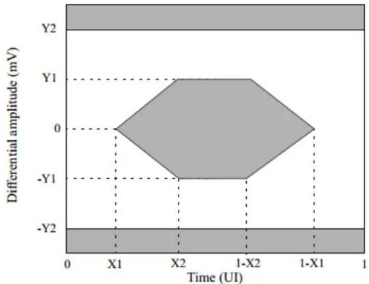
| Eye mask coordinates {X1, X2 Y1, Y2} | 0.11, 0.31 95, 350 | UI mV | 5 | |||
| Receiver (per Lane) | ||||||
| Single-ended output voltage | -0.3 | 4.0 | V | |||
| Differential data output swing | Vout,pp | 0 | 800 | mVpp | 6.7 | |
| AC common mode output voltage (RMS) | 7.5 | mV | ||||
| Termination mismatch at 1 MHx | 5 | % | ||||
| Differential output return loss | Per IEEE 802.3ba, Section 86A.4.2.1 | dB | 4 | |||
| Common mode output return loss | Per IEEE 802.3ba, Section 86A.4.2.2 | dB | 4 | |||
| Output transition time, 20% to 80% | 28 | ps | ||||
| J2 Jitter output | Jo2 | 0.42 | UI | |||
| J9 Jitter output | Jo9 | 0.65 | UI | |||
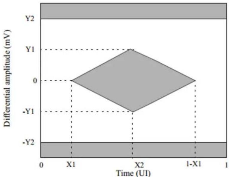
| Eye mask coordinates {X1, X2 Y1, Y2} | 0.29, 0.5 150, 425 | UI mV | 5 | |||
| Power Supply Ripple Tolerance | PSR | 50 | mVpp | |||
Notes:
- Maximum total power value is specified across the full temperature and voltage range.
- From power-on and end of any fault conditions.
- After internal AC coupling. Self-biasing 100Ω differential input.
- 10 MHz to 11.1 GHz range
- Hit ratio = 5 x 10E-5
- AC coupled with 100Ω differential output impedance.
- Settable in 4 discrete steps via the I2C interface. See Figure 2 for Vout settings.
radar
| Time (UI) | Differential amplitude (mV) | | --------- | --------------------------- | | 0 | 0 | | X1 | 0 | | X2 | 0 | | 1-X2 | 0 | | 1-X1 | 0 | | 1 | -Y2 |Figure 2 – Transmitter Input Differential Signal Mask
radar
| Time (UI) | Differential amplitude (mV) | | --------- | --------------------------- | | 0 | 0 | | X1 | 0 | | X2 | 0 | | 1-X1 | 0 | | 1 | 0 |Figure 3 – Receiver Output Differential Signal Mask
Receiver Output Amplitude Settings
| Code | Receiver Output Amplitude (mV) | Reference | ||
| 1xxxb | Min | Nominal | Max | |
| 0111b | 650 | 750 | 850 | |
| 0110b | 550 | 650 | 750 | |
| 0101b | 450 | 550 | 650 | Default Setting |
| 0100b | 350 | 450 | 550 | |
| 0011b | 300 | 400 | 500 | |
| 0010b | 250 | 350 | 450 | |
| 0001b | 200 | 300 | 400 | |
| 0000b | 150 | 250 | 350 | |
Receiver Pre-Emphasis Settings
| Code | Pre-emphasis (dB) | Reference |
| 0111b | 4.5 +/- 0.25 | |
| 0110b | 4.0 +/- 0.5 | |
| 0101b | 3.5 +/- 0.5 | |
| 0100b | 3.0 +/-0.5 | |
| 0011b | 2.5 +/- 0.5 | Default Setting |
| 0010b | 2.0 +/- 0.5 | |
| 0001b | 1.5 +/- 0.5 | |
| 0000b | 0.5 +/- 0.25 |
Module-end, Typical Power Consumption
| Power(mW) | Pre-Emphasis | ||||||||
| Code | 0000b | 0001b | 0010b | 0011b | 0100b | 0101b | 0110b | 0111b | |
| RxOutput | 0000b | 2006 | 2006 | 2009 | 2009 | 2009 | 2013 | 2013 | 2013 |
| 0001b | 2009 | 2009 | 2009 | 2013 | 2009 | 2013 | 2013 | 2016 | |
| 0010b | 2013 | 2013 | 2013 | 2013 | 2013 | 2016 | 2016 | 2020 | |
| 0011b | 2016 | 2013 | 2016 | 2016 | 2016 | 2020 | 2020 | 2023 | |
| 0100b | 2020 | 2016 | 2020 | 2020 | 2020 | 2020 | 2023 | 2023 | |
| 0101b | 2023 | 2020 | 2023 | 2023 | 2023 | 2026 | 2026 | 2026 | |
| 0110b | 2026 | 2026 | 2026 | 2026 | 2026 | 2026 | 2030 | 2030 | |
| 0111b | 2026 | 2026 | 2030 | 2030 | 2030 | 2030 | 2033 | 2033 | |
V. Optical Characteristics (T OP = 0 to 70°C, VCC = 3.3 ± 5% Volts)
| Parameter | Symbol | Min | Typ | Max | Unit | Ref. |
| Transmitter (per Lane) | ||||||
| Signaling Speed per Lane | 11.3 | GBd | 1 | |||
| Center wavelength | 840 | 860 | nm | |||
| RMS Spectral Width | SW | 0.65 | nm | |||
| Average Launch Power per Lane | TXP_x | -7.6 | 2.4 | dBm | ||
| Transmit OMA per Lane | TxOMA | -5.6 | 3.0 | dBm | 2 | |
| Difference in Power between any two lanes [OMA] | DP_x | 4.0 | dB | |||
| Peak Power per Lane | PP_x | 4.0 | dBm | |||
| Launch Power [OMA] minus TDP per Lane | P-TDP | -6.5 | dBm | |||
| TDP per Lane | TDP | 3.5 | dBm | |||
| Optical Extinction Ratio | ER | 3.0 | dB | |||
| Optical Return Loss Tolerance | ORL | 12 | dB | |||
| Encircled Flux | FLX | >86% at 19 um<30% at 4.5 um | dBm | |||
| Average launch power of OFF transmitter, per lane | -30 | dBm | ||||
| Relative Intensity Noise | RIN | -128 | dB/Hz | 3 | ||
| Transmitter eye mask definition {X1, X2, X3, Y1, Y2, Y3} | 0.23, 0.34, 0.43, 0.27, 0.35, 0.4 | |||||
| Receiver (per Lane) | ||||||
| Signaling Speed per Lane | 11.3 | GBd | 4 | |||
| Center wavelength | 840 | 860 | nm | |||
| Damage Threshold | DT | 3.4 | dBm | |||
| Average Receive Power per Lane | RXP_x | -9.5 | 2.4 | dBm | ||
| Receive Power (OMA) per Lane | RxOMA | 3.0 | dBm | |||
| Stressed Receiver Sensitivity (OMA) per Lane | SRS | -5.4 | dBm | |||
| Peak Power, per lane | PP_x | 4 | dBm | |||
| Receiver Reflectance | Rfl | -12 | dB | |||
| Vertical eye closure penalty, per lane | 1.9 | dB | ||||
| Stressed eye J2 jitter, per Lane | 0.3 | UI | ||||
| Stressed eye J9 jitter, per Lane | 0.47 | UI | ||||
| OMA of each aggressor lane | -0.4 | dBm | ||||
| Receiver jitter tolerance [OMA], per Lane | -5.4 | dBm | ||||
| Rx jitter tolerance: Jitter frequency and p-p amplitude | (75, 5) | kHz, UI | ||||
| (375, 1) | kHz, UI | |||||
| LOS De-Assert | LOS_D | -12.5 | dBm | |||
| LOS Assert | LOS_A | -30.0 | -15.5 | dBm | ||
| LOS Hysteresis | 1 | dB | ||||
Notes:
1. Transmitter consists of 12 lasers operating at a maximum rate of 11.3Gb/s each.
2. Even if TDP is <0.9dB, the OMA min must exceed this value.
3. RIN is scaled by 10*log (10/4) to maintain SNR outside of transmitter.
4. Receiver consists of 12 photodetectors operating at a maximum rate of 11.3Gb/s each.
VI. Memory Map and Control Registers
Compliant with the InfinibandSM Trade Association's InfiniBandTM Architectural Release 1.3, Volume 2, CXP Specification Release, November 6^th , 2012.
VII. Environmental Specifications
Finisar FTLD10CE3C transceiver modules have an operating temperature range from 0^ C to +70^ C case temperature.
| Environmental Specifications | Symbol | Min | Typ | Max | Units | Ref. |
| Case Operating Temperature | T_op | 0 | 70 | °C | ||
| Storage Temperature | T_sto | -5 | 75 | °C |
VIII. Regulatory Compliance
Finisar FTLD10CE3C transceiver modules are RoHS-6 Compliant. Copies of certificates are available at Finisar Corporation upon request.
FTLD10CE3C transceiver modules are classified as Class 1 laser eye safety compliant per IEC 60825-1.
| Feature | Agency | Standard | Certificate Number |
| Laser Eye Safety | FDA/CDRH | CDRH 21 CFR 1040 and Laser Notice 50 | 0620885-043 |
| Laser Eye Safety | TÜV | EN 60825-1: 2007, EN60825-2:2004+A1IEC 60825-1: 2007 ( 2^nd Edition)IEC 60825-2: 2010 ( 3^rd Edition) | R72120958 |
| Electrical Safety | TÜV | EN 60950:2006+A11 | R72120958 |
| Electrical Safety | UL/CSA | CLASS 3862.07CLASS 3862.87 | 2397145 |
Copies of the referenced certificates are available at Finisar Corporation upon request.
IX. Mechanical Specifications
The FTLD10CE3C transceiver module mechanical specifications are based on the CXP Specification.
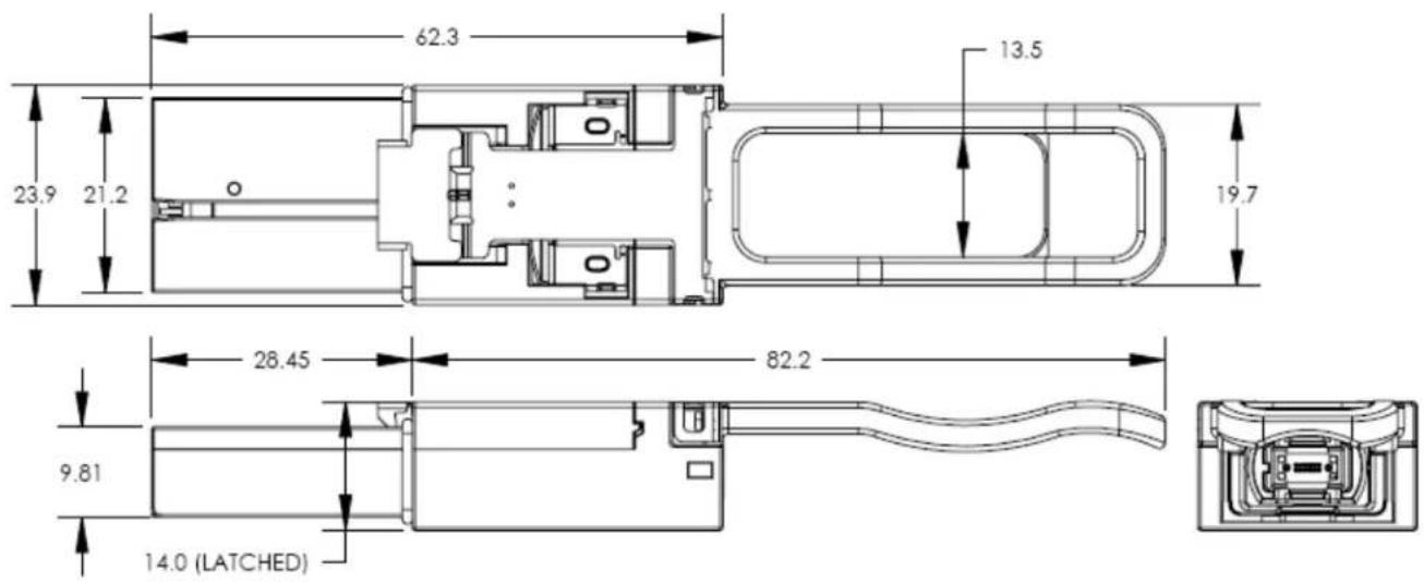
Figure 3 - FTLD10CE3C mechanical drawing
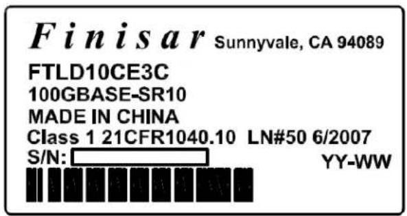
Figure 4 - FTLD10CE3C production-level product label
X. References
- Supplement to Infiniband Architecture Specification, Volume 2, Release 1.3., Annex A6: "12x Form-factor Pluggable (CXP) - Interface Specification for Cables, Active Cables, & Transceivers", November 6, 2012
- IEEE 802.3ba, PMD Type 100GBASE-SR10
- Directive 2002/95/EC of the European Council Parliament and of the Council, “on the restriction of the use of certain hazardous substances in electrical and electronic equipment”. January 27, 2003.
- “Application Note AN-2038: Finisar Implementation Of RoHS Compliant Transceivers”, Finisar Corporation.
- “Application Note AN-2085: CXP Transceiver EEPROM Mapping”, Finisar Corporation.
XI. For More Information
Finisar Corporation
1389 Moffett Park Drive
Sunnyvale, CA 94089-1133
Tel. 1-408-548-1000
Fax 1-408-541-6138
sales@finisar.com
www.finisar.com