FTLQ1381N7NL - Composant optique Finisar - Free user manual and instructions
Find the device manual for free FTLQ1381N7NL Finisar in PDF.

User questions about FTLQ1381N7NL Finisar
0 question about this device. Answer the ones you know or ask your own.
Ask a new question about this device
Download the instructions for your Composant optique in PDF format for free! Find your manual FTLQ1381N7NL - Finisar and take your electronic device back in hand. On this page are published all the documents necessary for the use of your device. FTLQ1381N7NL by Finisar.
USER MANUAL FTLQ1381N7NL Finisar
Product Specification
40G NRZ VSR Multi-Rate CFP Optical Transceiver Module
FTLQ1381N7NL
PRODUCT FEATURES
• Hot-pluggable CFP form factor
• Supports 39.8 Gb/s to 44.6 Gb/s data rates
• Power dissipation < 8W (class 1)
• RoHS-6 compliant (lead-free)
• Commercial temperature range 0°C to 70°C
- Single 3.3V power supply
• Maximum link length of 2km on Single Mode Fiber (SMF)
• 4x10G MLD electrical interface
- Duplex fiber receptacles
• Built-in digital diagnostic functions
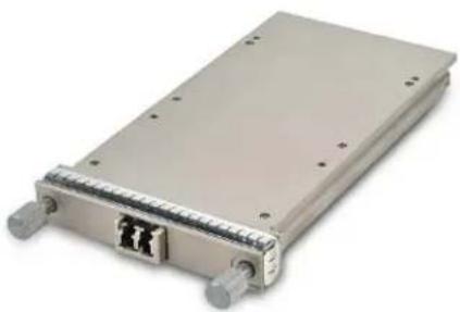
natural_image
Exterior view of a metallic electronic device with ports and connectors (no visible text or symbols)SUPPORTED STANDARDS
• SONET OC-768/ SDH STM-256
• 40GBASE-FR (40G Ethernet)
• OTN (OTU3 short reach)
- OTU3e1 and OTU3e2
Finisar's FTLQ1381N7NL 40G CFP transceiver modules are designed for use in 40 Gigabit links required for router to router client side applications or uplink interconnections to transport networks. Designed to enable optical compatibility with existing carrier client interfaces VSR2000-3R2 per ITU-T G.693, they are compliant with the CFP MSA ^1 , IEEE 802.3bg 40GBASE-FR ^2 and OTU3 requirements specified in ITU-T G.709. Digital diagnostics functions are available via an MDIO interface, as specified by the CFP MSA. The optical transceiver is compliant per the RoHS Directive 2011/65/EU ^3 . See Finisar Application Note AN-2038 for more details ^4 .
PRODUCT SELECTION
FTLQ1381x7yz
x: E: Ethernet only (41.25Gb/s) N: Multi-rate support up to 43.1Gb/s (default) M: Multi-rate support up to 44.6Gb/s
7: 1550nm NRZ optical
y: N: Flat top (default configuration per MSA)
z: L: LC straight receptacle (default configuration)
A: LC 45 degree angled receptacle
S: SC straight receptacle
I. General Description
The FTL1381N7NL is based on the CFP Multi-Source Agreement (MSA ^1 ), which defines the form factor of an optical transceiver that can support 40Gbit/s interfaces for Ethernet, Telecommunications standards or other interconnect applications. The nominal signaling lane rate is 10Gbit/s per lane and supports XLAUI, OTL3.4, and STL256.4 electrical interface specifications.
Supported aggregate data rates range from 39.8Gb/s (SONET OC-768/SDH STM-256 ^ ) up to 44.6Gb/s (OTU3c). The module requires a system reference clock at electrical lane-rate divided by 64 (155MHz) or divided by 16 (622MHz). During power up or hot plug insertion the reference clock must be present in the low power mode to ensure compliant locking behavior upon start up; if the clock is not present or subsequently removed during module provisioning, Finisar recommends performing a module reset. To ensure correct module operation the Tx and Rx reference clock registers must be set to match the supplied reference clock frequency. The module has the option to incorporate a clock jitter filter based on a narrow-band PLL.
This 40G NRZ CFP was designed to support very short reach (VSR) optical networking connections characterized by single mode fiber link lengths from 2m to 2 km. The FTL1381 was developed to support 40GBASE–FR PMD but is also intended to be compliant with application VSR2000-3R2 as defined in ITU-T G.693.
The CFP module is designed to be hot pluggable and the host system or the module shall not be damaged by insertion or removal of the module. The electrical interface consists of a 148-pin connector and support real-time control functions via the hardware pins. The monitoring, alarms†† and control functions are supported via an MDIO bus and the module is designed to operate from 0°C to +70°C case temperature. The power consumption meets class 1 power requirements of 8W. The optional loopback functionality defined by the MSA ^1 is not supported.
† Note: For modules with Hardware Rev 1.2 or lower, the maximum supported lane to lane offset is 2 bytes (32 bytes of lane offset is supported with HW Rev 1.3 or higher); therefore during module operation in SDH mode per G.707 Amendment 2 it is recommended to ensure the framer is set to operate with 0 bytes of time offset between lanes.
††Note: TX_LOSF alarm is defined as the logical OR of TX_FIFO_ERROR, TX_LOCK_ERROR and TX_OUT_OF_ALIGNMENT. The TX_OUT_OF_ALIGNMENT Alarm will be muted when operating on Gigabit Ethernet mode.
II. Pin Description
Per CFP MSA ^1 , Table 5-6 and 5-7.
| Top Row | Bottom Row | Top Row | Bottom Row | ||||
| 148 | GND | 1 | 3.3V_GND | 111 | GND | 38 | MOD_ABS |
| 147 | REFCLKn | 2 | 3.3V_GND | 110 | N.C. | 39 | MOD_RSTn |
| 146 | REFCLKp | 3 | 3.3V_GND | 109 | N.C. | 40 | RX_LOS |
| 145 | GND | 4 | 3.3V_GND | 108 | GND | 41 | GLB_ALRMn |
| 144 | N.C. | 5 | 3.3V_GND | 107 | N.C. | 42 | PRTADR4 |
| 143 | N.C. | 6 | 3.3V | 106 | N.C. | 43 | PRTADR3 |
| 142 | GND | 7 | 3.3V | 105 | GND | 44 | PRTADR2 |
| 141 | N.C. | 8 | 3.3V | 104 | N.C. | 45 | PRTADR1 |
| 140 | N.C. | 9 | 3.3V | 103 | N.C. | 46 | PRTADR0 |
| 139 | GND | 10 | 3.3V | 102 | GND | 47 | MDIO |
| 138 | N.C. | 11 | 3.3V | 101 | N.C. | 48 | MDC |
| 137 | N.C. | 12 | 3.3V | 100 | N.C. | 49 | GND |
| 136 | GND | 13 | 3.3V | 99 | GND | 50 | VND_IO_F |
| 135 | N.C. | 14 | 3.3V | 98 | N.C. | 51 | VND_IO_G |
| 134 | N.C. | 15 | 3.3V | 97 | N.C. | 52 | GND |
| 133 | GND | 16 | 3.3V_GND | 96 | GND | 53 | VND_IO_H |
| 132 | N.C. | 17 | 3.3V_GND | 95 | N.C. | 54 | VND_IO_J |
| 131 | N.C. | 18 | 3.3V_GND | 94 | N.C. | 55 | 3.3V_GND |
| 130 | GND | 19 | 3.3V_GND | 93 | GND | 56 | 3.3V_GND |
| 129 | N.C. | 20 | 3.3V_GND | 92 | N.C. | 57 | 3.3V_GND |
| 128 | N.C. | 21 | VND_IO_A | 91 | N.C. | 58 | 3.3V_GND |
| 127 | GND | 22 | VND_IO_B | 90 | GND | 59 | 3.3V_GND |
| 126 | N.C. | 23 | GND | 89 | RX3n | 60 | 3.3V |
| 125 | N.C. | 24 | TX_MCLKn | 88 | RX3p | 61 | 3.3V |
| 124 | GND | 25 | TX_MCLKp | 87 | GND | 62 | 3.3V |
| 123 | TX3n | 26 | GND | 86 | RX2n | 63 | 3.3V |
| 122 | TX3p | 27 | VND_IO_C | 85 | RX2p | 64 | 3.3V |
| 121 | GND | 28 | VND_IO_D | 84 | GND | 65 | 3.3V |
| 120 | TX2n | 29 | VND_IO_E | 83 | RX1n | 66 | 3.3V |
| 119 | TX2p | 30 | PRG_CNTL1 | 82 | RX1p | 67 | 3.3V |
| 118 | GND | 31 | PRG_CNTL2 | 81 | GND | 68 | 3.3V |
| 117 | TX1n | 32 | PRG_CNTL3 | 80 | RX0n | 69 | 3.3V |
| 116 | TX1p | 33 | PRG_ALRM1 | 79 | RX0p | 70 | 3.3V_GND |
| 115 | GND | 34 | PRG_ALRM2 | 78 | GND | 71 | 3.3V_GND |
| 114 | TX0n | 35 | PRG_ALRM3 | 77 | RX_MCLKn | 72 | 3.3V_GND |
| 113 | TX0p | 36 | TX_DIS | 76 | RX_MCLKp | 73 | 3.3V_GND |
| 112 | GND | 37 | MOD_LOPWR | 75 | GND | 74 | 3.3V_GND |
Bottom Row Pin Description
| PIN # | Name | I/O | Logic | Description |
| 1 | 3.3V_GND | 3.3V Module Supply Voltage Return Ground, internally connected to Signal Ground | ||
| 2 | 3.3V_GND | |||
| 3 | 3.3V_GND | |||
| 4 | 3.3V_GND | |||
| 5 | 3.3V_GND | |||
| 6 3 | 3.3V 3.3V Module Supply Voltage | |||
| 7 3 | 3.3V 3.3V Module Supply Voltage | |||
| 8 3 | 3.3V 3.3V Module Supply Voltage | |||
| 9 3 | 3.3V 3.3V Module Supply Voltage | |||
| 10 3 | 3.3V 3.3V Module Supply Voltage | |||
| 11 3 | 3.3V 3.3V Module Supply Voltage | |||
| 12 3 | 3.3V 3.3V Module Supply Voltage | |||
| 13 3 | 3.3V 3.3V Module Supply Voltage | |||
| 14 3 | 3.3V 3.3V Module Supply Voltage | |||
| 15 3 | 3.3V 3.3V Module Supply Voltage | |||
| 16 | 3.3V_GND | 3.3V Module Supply Voltage Return Ground, internally connected to Signal Ground | ||
| 17 | 3.3V_GND | |||
| 18 | 3.3V_GND | |||
| 19 | 3.3V_GND | |||
| 20 | 3.3V_GND | |||
| 21 | VND_IO_A | I/O | Module Vendor I/O A. Do Not Connect! | |
| 22 | VND_IO_B | I/O | Module Vendor I/O B. Do Not Connect! | |
| 23 | GND | |||
| 24 | TX_MCLKn | O CML Tx Monitor clock | ||
| 25 | TX_MCLKp | O CML Rx Monitor cloc k | ||
| 26 | GND | |||
| 27 | VND_IO_C | I/O | Module Vendor I/O C. Do Not Connect! | |
| 28 | VND_IO_D | I/O | Module Vendor I/O D. Do Not Connect! | |
| 29 | VND_IO_E | I/O | Module Vendor I/O E. Do Not Connect! | |
| 30 | PRG_CNTL1 | I | LVCMOS w/ PUR | Programmable Control 1 set over MDIO, Default: TRXIC_RSTn, TX & RX ICs reset, "0": reset; "1" or NC: enabled (i.e., not used). |
| 31 | PRG_CNTL2 | I | LVCMOS w/ PUR | Programmable Control 2 set over MDIO, Default: Hardware Interlock LSB, "00": ≤8W; "01": ≤16W; "10": ≤24W; "11" or NC: ≤32W (i.e., not used). |
| 32 | PRG_CNTL3 | I | LVCMOS w/ PUR | Programmable Control 3 set over MDIO, Default: Hardware Interlock MSB, "00": ≤8W; "01": ≤16W; "10": ≤24W; "11" or NC: ≤32W (i.e., not used). |
| 33 | PRG_ALRM1 | O | LVCMOS | Programmable Alarm 1 set over MDIO, Default: HIPWR_ON, "1": module power up completed; "0": module not high powered up. |
| 34 | PRG_ALRM2 | O | LVCMOS | Programmable Alarm 2 set over MDIO, Default: MOD_READY, "1": Ready; "0": not Ready. |
| 35 | PRG_ALRM3 | O | LVCMOS | Programmable Alarm 3 set over MDIO, Default: MOD_FAULT, fault detected, "1": Fault; "0": No Fault. |
| 36 | TX_DIS | I | LVCMOS w/ PUR | Transmitter Disable for all lanes, "1" or NC = transmitter disabled, "0" = transmitter enabled |
| 37 | MOD_LOPWR | I | LVCMOS w/ PUR | Module Low Power Mode, "1" or NC: module in low power (safe) mode, "0": power-on enabled |
| 38 | MOD_ABS | O | GND | Module Absent, "1" or NC: module absent, "0": module present, Pull Up Resistor on Host |
| 39 | MOD_RSTn I LVCMOS w/ PDR | Module Reset. "0" resets the module, "1" or NC = module enabled, Pull Down Resistor in Module | ||
| 40 | RX_LOS | O | LVCMOS | Receiver Loss of Optical Signal, "1": low optical signal, "0": normal condition |
| 41 | GLB_ALRMn | O | LVCMOS | Global Alarm. "0": alarm condition in any MDIO Alarm register, "1": no alarm condition, Open Drain, Pull Up Resistor on Host |
| 42 | PRTADR4 | I 1.2V CMOS | MDIO Physical Port address bit 4 | |
| 43 | PRTADR3 | I 1.2V CMOS | MDIO Physical Port address bit 3 | |
| 44 | PRTADR2 | I 1.2V CMOS | MDIO Physical Port address bit 2 | |
| 45 | PRTADR1 | I 1.2V CMOS | MDIO Physical Port address bit 1 | |
| 46 | PRTADR0 | I 1.2V CMOS | MDIO Physical Port address bit 0 | |
| 47 | MDIO | I/O | 1.2V CMOS | Management Data I/O bi-directional data (electrical specs as per 802.3ae and ba) |
| 48 | MDC | I | 1.2V CMOS | Management Data Clock (electrical specs as per 802.3ae and ba) |
| 49 | GND | |||
| 50 | VND_IO_F | I/O | Module Vendor I/O F. Do Not Connect! | |
| 51 | VND_IO_G | I/O | Module Vendor I/O G. Do Not Connect! | |
| 52 | GND | |||
| 53 | VND_IO_H | I/O | Module Vendor I/O H. Do Not Connect! | |
| 54 | VND_IO_J | I/O | Module Vendor I/O J. Do Not Connect! | |
| 55 | 3.3V_GND | 3.3V Module Supply Voltage Return Ground, internally connected to Signal Ground | ||
| 56 | 3.3V_GND | |||
| 57 | 3.3V_GND | |||
| 58 | 3.3V_GND | |||
| 59 | 3.3V_GND | |||
| 60 | 3.3V | 3.3V Module Supply Voltage | ||
| 61 | 3.3V | |||
| 62 | 3.3V | |||
| 63 | 3.3V | |||
| 64 | 3.3V | |||
| 65 | 3.3V | |||
| 66 | 3.3V | |||
| 67 | 3.3V | |||
| 68 | 3.3V | |||
| 69 | 3.3V | |||
| 70 | 3.3V_GND | 3.3V Module Supply Voltage Return Ground, internally connected to Signal Ground | ||
| 71 | 3.3V_GND | |||
| 72 | 3.3V_GND | |||
| 73 | 3.3V_GND | |||
| 74 | 3.3V_GND | |||
III. Absolute Maximum Ratings
Exceeding the limits below may damage the transceiver module permanently.
| Parameter | Symbol | Min | Typ | ||
| Maximum Supply Voltage Vcc -0.5 3.6 | V | ||||
| Storage Temperature | T_S | -40 | 85 | °C | |
| Case Temperature | T_Case | -10 | 75 | °C | 1 |
| Relative Humidity | RH | 0 | 85 | % | 2 |
| Static discharge voltage (human body model) | ESD | 500 | V | ||
| Receiver Damage Threshold (PIN/TIA) | P_Rdmg | +6 | dBm | ||
| Module initialization time (MDIO) | T_initialize | 2.5 | s | 3,4 |
Notes:
- See section VII for Operating conditions.
- Non-condensing.
- Initialization time from cold start or module reset (MOD_RSTn). Maximum time for module to enter Low-Power state.
- During power up or hot plug insertion the reference clock must be present in low power mode to ensure compliant module power-up.
IV. Electrical Characteristics ( T_OP = 0 to 70 °C, V_CC = 3.2 to 3.4 Volts)
| Parameter | Symbol | Min | Typ | Max | Unit | Ref. |
| Voltage Power Supply | ||||||
| Supply Voltage | Vcc | 3.2 | 3.4 | V | ||
| Supply Current | Icc | 2.5 | A | |||
| Module total power | P | 8 | W | 1 | ||
| Low Power mode Dissipation | P_LOW | 2 | W | |||
| Inrush Current (class 1) | I_INRUSH | 50 | mA/usec | |||
| Turn-off current (class 1) | I_TURNOFF | -50 | ||||
| Power Supply Ripple | V_RIP | 2%3% | DC-1MHz1-10MHz | |||
| Optical Transmitter Direction | ||||||
| Signaling rate per lane | 9.95 | 11.15 | Gb/s | |||
| Min AC Common-mode voltage | 20 | mV | ||||
| Input differential impedance | R_in | 80 | 100 | 120 | Ω | 2 |
| Data input rise and fall time tolerance | t_r/t_f | 24 | ps | 3 | ||
| Minimum total Jitter tolerance | 0.62 | UI | ||||
| Minimum deterministic Jitter tolerance | 0.42 | UI | ||||
| Module Electrical input eye mask definition | {X1, X2}{Y1, Y2} | {0.31, 0.5}{42.5, 425} | UImV | 5 | ||
| Optical Receiver Direction | ||||||
| Signaling rate per lane | 9.95 | 11.15 | Gb/s | |||
| Max AC Common-mode voltage | 15 | mV | ||||
| Differential data output swing per lane | Vout,pp | 760 | mV | 4 | ||
| Data output rise and fall time | t_r/t_f | 24 | ps | 3 | ||
| Maximum total Jitter | 0.4 | UI | ||||
| Maximum deterministic Jitter | 0.25 | UI | ||||
| Module Electrical output eye mask definition | {X1, X2}{Y1, Y2} | {0.2, 0.5}{136, 380} | UImV | 5 | ||
Notes:
- Maximum total power value is specified across the full temperature and voltage range.
- After internal AC coupling.
- 20% to 80%.
- Host is expected to be compliant with IEEE 802.3bg, clause 83A.
- Pre-emphasis must be turned off for jitter and eye mask measurements (section 83A.3.3.5 of IEEE 802.03bg).
V. Optical Characteristics = 0 to (70 °C, Vcc = 3.2 to 3.4 Volts).
All specifications are EOL (End of Life) and will be met over the range of standard operating conditions unless otherwise specified.
| Parameter | Symbol | Min | Typ | |||
| Transmitter | ||||||
| Signaling Speed | BR | 39.8 | 44.6 | Gb/s | 1 | |
| Lane center wavelengths (range) | _c | 1530 | 1565 | nm | ||
| Spectral width | SW | 1 | nm | |||
| Average Launch Power | P_OUT | 0 | 3.0 | dBm | ||
| Optical Extinction Ratio | ER | 8.2 | dB | |||
| Eye crossing | 40 60 | % | ||||
| Side Mode Suppression Ratio | SMSR | 35 | dB | |||
| Average launch power (transmitter OFF) | -30 | dBm | ||||
| Relative Intensity Noise | RIN | -128 | dB/Hz | 2 | ||
| Transmitter Return Loss | 27 | dB | ||||
| Transmitter eye mask definition {X1, X2, X3, Y1, Y2, Y3} | {0.25, 0.4, 0.45, 0.25, 0.28, 0.4} / ITU G.693 Complaint | 3 | ||||
| Jitter Generation compliance | J_GEN | Conforms to G.783 and G.8251 | UI_PP | |||
Max
| Parameter | Symbol | Min | Max | Min | Max | Unit | Ref. |
| Receiver | |||||||
| Applicable Date Rate | BR | 39.8 to 41.25 | 43.1 to 44.6 | Gb/s | 1 | ||
| Wavelength input range | 1520 | 1580 | 1520 | 1580 | nm | 4 | |
| Receiver Sensitivity at 10^-12 , B2B | S | -7 | N/A | N/A | dBm | ||
| Receiver Sensitivity at 10^-7 , B2B | S | N/A | N/A | -7 | dBm | ||
| Dispersion Penalty (40ps/nm) at 10^-12 | D_p | 2 | N/A | N/A | dB | ||
| Dispersion penalty (40ps/nm) at pre-FEC BER 10^-7 | D_p | N/A | N/A | 2 | dB | ||
| Receiver Overload | P_MAX | 3 | 3 | dBm | |||
| Maximum Reflectance of Receiver | RL | 27 | 27 | dB | |||
| Jitter Tolerance compliance | ITU-T G.825 | ITU-T G.8251 | |||||
| RX_LOS Assert level | LOS_A | -15 | -12 | -15 | -12 | dBm | 5,6 |
| RX_LOS Hysteresis | 0.4 | 2.0 | 0.4 | 2.0 | dB | 5 | |
Notes:
- Consult product ordering guide for data rate selection. Supports 40GBASE-FR and XLAUI per IEEE 802.3bg, OTU3 per ITU-T Rec. G.695 and G.709, STL256.4/OTL3.4 (MLD), and OTU3c1/OTU3c2 per ITU-T G-Series Rec. Supplement 43.
- RIN is scaled by 10*log(10/4) to maintain SNR outside of transmitter.
- Eye mask measured with 1000 waveforms.
- The receiver responsivity range supports 1310nm but the module is not tested at 1310nm and the performance cannot be guaranteed if operated at 1310nm.
- Measured based on received optical power for accuracy (default). Can be configured based on Rx Lock Error for fast response time; optical power levels in the table will be not applicable in this configuration.
- Output termination of the RX_LOS hardware pin is an active push-pull. There is no internal pull-up or pull-down.
VI. General Specifications
Monitor Accuracy, Timing parameters and Clock characteristics
| Parameter | Symbol/ Measurement Range | Min | Max | Units | Ref. | |
| Maximum Supported Distances | ||||||
| Fiber type SMF L | max | 2.4 | km | |||
| Monitor Accuracy | ||||||
| Receiver Power Monitor (RxPowMon) -10 to +4dBm -0.5 | +0.5 | dB | ||||
| Receiver Power Monitor (RxPowMon) | -14 to -10dBm | -1.0 | +1.0 | dB | ||
| Transmitter Power Monitor (TxPowMon) | -1 to +4dBm | -0.5 | +0.5 | dB | ||
| Laser Bias Monitor (LsBiasMon) | +20 to +100mA | -10 | +10 | mA | ||
| Temperature measurements (internal) | -5 to 75C | -3 | +3 | C | ||
| Power supply voltage | +3.1 to +3.5V | -100 | +100 | mV | ||
| Timing Parameters | ||||||
| Rx LOS Assert time | t_loss_assert | 500 | us | 1 | ||
| Rx LOS De-Assert time | t_loss_deassert | 500 | us | 1 | ||
| Tx Disable time (TX_DIS) | t_assert | 100 | us | 2 | ||
| Tx Enable time (TX_DIS) | t_deassert | 100 | ms | 2 | ||
| Laser output ready from low power state | L_Ready | 30 | s | 3 | ||
| Global Alarm Assert delay time | GLB_ALRMn | 150 | ms | 4 | ||
| Global Alarm De-Assert delay time | GLB_ALRMn | 150 | ms | 4 | ||
| Hardware MOD-LOPWR Assert | t_mod_lopwr_assert | 10 | ms | 7 | ||
| CML Reference Clock Characteristics | ||||||
| Impedance | Z_D | 80 | 120 | Ω | ||
| Clock duty Cycle | 40 | 60 % | ||||
| Output Differential Voltage (p-p) | V_DIFF | 400 | 1200 | mV | ||
| Frequency | 1/64 Electrical lane rate | F_REF | 155.47 | 174.22 | MHz | 5 |
| 1/16 Electrical lane rate | 621.87 | 696.88 | ||||
| Frequency Stability | Δf (XLAUI) | -100 | +100 | ppm | ||
| Δf (STL256.4/OTL3.4) | -20 | +20 | ppm | |||
| Coupling | AC Coupled | |||||
| CML Tx/Rx Monitor Characteristics | ||||||
| Impedance | Z_D | 80 | 120 | Ω | ||
| Clock duty Cycle | 40 | 60 % | ||||
| Output Differential Voltage (p-p) | V_DIFF | 400 | 1200 | mV | ||
| Frequency | 1/64 Optical lane rate | F_REF | 621.87 | 696.88 | MHz | 6 |
| 1/16 Optical lane rate | 2.487 | 2.787 | GHz | |||
| 1/64 Network lane rate | 155.47 | 174.22 | MHz | |||
| Coupling | AC Coupled | |||||
Notes:
- Measured based on received optical power for accuracy (default). Can be configured based on Rx Lock Error for speed.
- From laser steady state condition.
- Laser output power enabled from low-power state (Typically under 10s at room temperature).
- Logical "or" of associated MDIO alarm and status registers.
- Selectable via MDIO; default rate set at 1/16 of Electrical lane rate per MSA Rev 1.4.
- Selectable via MDIO; default rate set at 1/16 of Optical lane rate.
- MSA specification is 1ms.
Alarm/Warning Levels for Threshold Registers
| Parameter | Operating | Range | Low | High | |
| Monitor Alarm/Warning threshold levels | |||||
| Module Temperature Alarm -4 74 °C | |||||
| Module Temperature Warning | 0 | 70 | °C | ||
| Power supply voltage Alarm | 3.135 | 3.465 | V | ||
| Power supply voltage Warning | 3.200 | 3.400 | V | ||
| SOA Bias current Alarm | Not applicable | ||||
| SOA Bias current Warning | Not applicable | ||||
| Laser bias current Alarm | 15 | 80 | mA | ||
| Laser bias current Warning | 20 | 75 | mA | ||
| Tx Output Power Alarm | -1 | +4 | dBm | ||
| Tx Output Power Warning | 0 | +3 | dBm | ||
| Laser Temperature Alarm | 10 | 50 °C | |||
| Laser Temperature Warning | 20 | 40 | °C | ||
| Rx Optical Power Alarm | -14 | +3.5 | dBm | ||
| Rx Optical Power Warning | -10 | +3 | dBm | ||
Units Ref.
VII. Environmental Specifications
Finisar FTLQ1381 CFP transceivers have a commercial operating temperature range from 0^ C to +70^ C case temperature.
| Parameter | Symbol | Min | Typ | Max | Units | Ref. |
| Case Operating Temperature | T_op | 0 | 70 | °C | 1 | |
| Storage Temperature | T_sto | -40 | 85 | °C |
- Performance is not guaranteed when operating outside specified range. Performance between 70^ C and 75^ C is not guaranteed.
VIII. Regulatory Compliance
Finisar FTLQ1381 CFP transceivers are Class 1 Laser Products. They are certified per the following standards:
| Feature | Agency | Standard | Certificate | Number |
| Laser Eye Safety | FDA/CDRH | CDRH 21 CFR 1040 and Laser Notice 50 | 9210176 | |
| Laser Eye Safety | TÜV | EN | 60825-1: 1994+AIEC 60825-1: 1993+A1:1997+A2:2001IEC 60825-2: 2000, Edition 2 | 11:1096+1022+2001 |
| Electrical Safety | TÜV | EN | 60950 | |
| Electrical Safety | UL/CSA | CLASS 3862.07CLASS 3862.87 | 2375840 (LR 115314) | |
Copies of the referenced certificates are available at Finisar Corporation upon request.
IX. Digital Diagnostic Functions
The FTLQ1381CFP transceivers support the MDIO-based diagnostics interface specified in the CFP MSA ^1 . See Finisar Application Note AN-2078.
X. Memory Contents and Supported Functionality
Per the CFP MSA ^1 .
Please see Finisar Application Note AN-2091 for details of non-volatile registers (NVR) and supported MDIO functions.
XI. Host PCB Layout and Bezel Recommendations
Per CFP MSA Hardware Specification, Rev 1.4 ^1 .
XII. Mechanical Specifications
Finisar FTLQ1381 CFP transceivers are compatible with the CFP MSA specification for 40G/100G pluggable form factor modules.
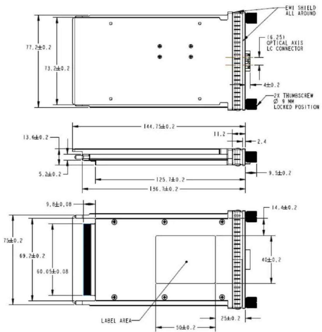
Figure 1. FTLQ1381 Outline Mechanical Dimensions (LC-straight connector).
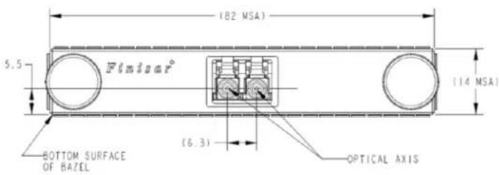
Figure 2. FTLQ1381 Mechanical Dimensions of LC-Straight connector.
Figure 3. FTLQ1381 Mechanical Dimensions of LC-Angled connector.
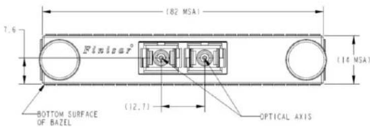
Figure 4. FTLQ1381 Mechanical Dimensions of SC-Straight connector.
Finisar Sunnyvale, CA 94089
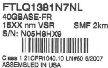
Figure 5. Product Label example.
XIII. References
- CFP MSA Hardware Specification, Rev 1.4 and Management Interface Specifications, Rev 2.2., www.cfp-msa.org
- IEEE 802.3bg, PMD Type 40GBASE-FR.
- Directive 2002/95/EC of the European Council Parliament and of the Council, “on the restriction of the use of certain hazardous substances in electrical and electronic equipment”
- “Application Note AN-2038: Finisar Implementation of RoHS Compliant Transceivers”
- “Application Note AN-2091: NVR1 and MDIO Compatibility List, 40GE Base FR (FTLQ1381), Finisar Corporation, Rev 04, February 2013.
XIV. Revision History
| Revision | Date | Description |
| A00 Apr 28, 2011 Draft document created. | ||
| A01 Feb 1, 2012 Initial document (Limited release - product not yet released for production) | ||
| A02 July 15, 2012 Page 2, added footnote on TX_LOSF alarm definition.Page 6, change rise/fall time to correct column (Min).Page 8, change measurement range of Tx optical power to -1 to +4dBm.Page 8, added timing for Hardware MOD_LOPWR Assert time.Page 9, Rx optical power alarm changed to +3.5dBm.Page 12, added figure with SC connector. | ||
| A03 | October 31, 2012 | Page 2, updated definition of lane offset in footnote.Page 7, changed LOS Hysteresis value from 0.25dB to 0.4dB.Page 10, updated certificate numbers.Page 13, updated Application note AN-2091 release date to October 31.Page 13, updated Management interface specification to 2.2. |
| A04 | April 25, 2013 | Page 7, clarification on RX_LOS output circuit in foot note. |
| A05 | August 25, 2014 | Footer, removed “Confidential” label. |
| B1 | October 9, 2015 | Updated logo and RoHS statement |
For More Information
Finisar Corporation
1389 Moffett Park Drive
Sunnyvale, CA 94089-1133
Tel. 1-408-548-1000
Fax 1-408-541-6138
sales@finisar.com
www.finisar.com