FTLX1812M3BNL - Unspecified Finisar - Free user manual and instructions
Find the device manual for free FTLX1812M3BNL Finisar in PDF.

User questions about FTLX1812M3BNL Finisar
0 question about this device. Answer the ones you know or ask your own.
Ask a new question about this device
Download the instructions for your Unspecified in PDF format for free! Find your manual FTLX1812M3BNL - Finisar and take your electronic device back in hand. On this page are published all the documents necessary for the use of your device. FTLX1812M3BNL by Finisar.
USER MANUAL FTLX1812M3BNL Finisar
Preliminary Product Specification
Extended Temperature, 10Gb/s 80km TDM XFP Optical Transceiver
FTLX1812M3BNL
PRODUCT FEATURES
• Supports 8.5Gb/s to 11.3Gb/s bit rates
• Hot-pluggable XFP footprint
• Maximum link length of 80km
• RoHS-6 compliant (lead-free)
• Temperature-stabilized EML transmitter
- Duplex LC connector
• Power dissipation <3.5W
• Built-in digital diagnostic functions
• XFI Loop-back Support
- CDR bypass mode for <8Gb/s or legacy 8GFC XFP applications
• Temperature range: -5^ to 85^
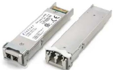
natural_image
Two metallic electronic devices with ports and connectors, no visible text or symbols on the main body.APPLICATIONS
• S ONET OC-192 / SDH STM-64
ITU-T G.959.1 P1L1-2D2
• IE EE 802.3ae 10GBASE-ZR/ZW 80km 10G Ethernet
• E xtended 80km, 10GFC 1200-SM-LL-L and 8GFC, 800-SM-LC-L
• S upports OTN/ITU-T G.709 FEC protocols OTU1e, OTU2, and OTU2e
• 1 0G CPRI
Finisar's 80km FTLX1812M3B NL Small Form Factor 10Gb/s (XFP) transceivers comply with the current XFP Multi-Source Agreement (MSA) Specification ^1 . They are a true multi-protocol transceiver complying with 80km SONET OC-192 and SDH STM-64 per ITU-T G.959.1: P1L1-2D2, and also support 10GBASE-ZR/ZW 80km 10-Gigabit Ethernet, 10-Gigabit Fibre Channel 1200-SM-LL-L, and all ITU-T G.709 OTN/FEC (protocols up to 11.32Gb/s. The transceiver is also capable of supporting 8GFC, 800-SM-LC-L, with full compliance to the Tx & Rx electrical jitter specifications by adjusting a “rate select” bit through the I ^2 C interface. Digital diagnostics functions are available via a 2-wire serial interface, as specified in the XFP MSA. The transceiver is RoHS compliant and lead free per Directive 2002/95/EC ^3 , and Finisar Application Note AN-2038 ^4 .
PRODUCT SELECTION
FTLX1812M3BNL
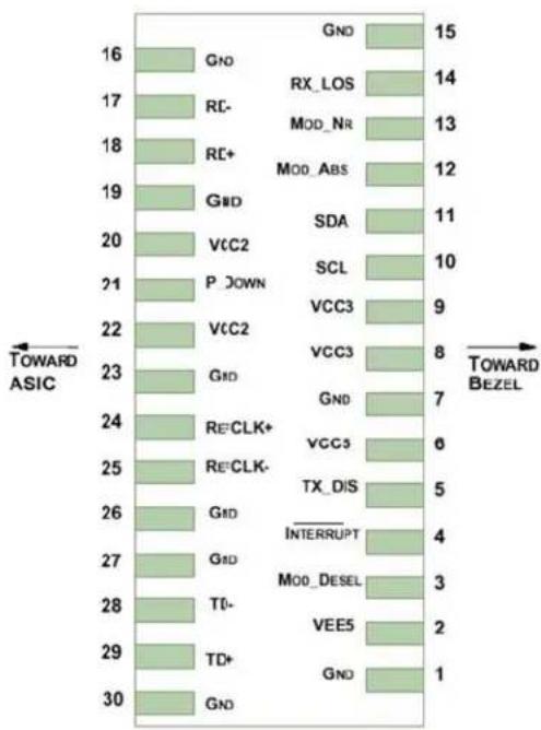
I. Pin Descriptions
| Pin | Logic | Symbol | Name/Description | Ref. | |
| 1 | GND | Module | Ground | 1 | |
| 2 | VEE5 Optional | -5.2 Power Supply - Not required | |||
| 3 | LVTTL-I | Mod-Desel | Module De-select; When held low allows the module to respond to 2-wire serial interface commands | ||
| 4 | LVTTL-O | Interrupt | Interrupt (bar); Indicates presence of an important condition which can be read over the serial 2-wire interface | 2 | |
| 5 | LVTTL-I | TX_DIS | Transmitter Disable; Transmitter laser source turned off | ||
| 6 | VCC5 | +5 Power Supply | |||
| 7 | GND | Module | Ground | 1 | |
| 8 | VCC3 | +3.3V | Power | Supply | |
| 9 | VCC3 | +3.3V | Power | Supply | |
| 10 | LVTTL-I | SCL | Serial 2-wire interface clock | 2 | |
| 11 | LVTTL-I/O | SDA | Serial 2-wire interface data line | 2 | |
| 12 | LVTTL-O | Mod_Abs | Module Absent; Indicates module is not present. Grounded in the module. | 2 | |
| 13 | LVTTL-O | Mod_NR | Module Not Ready; Finisar defines it as a logical OR between RX_LOS and Loss of Lock in TX/RX. | 2 | |
| 14 | LVTTL-O | RX_LOS | Receiver Loss of Signal indicator | 2 | |
| 15 | GND | Module Ground | 1 | ||
| 16 | GND | Module Ground | 1 | ||
| 17 | CML-O | RD- | Receiver inverted data output | ||
| 18 | CML-O | RD+ | Receiver non-inverted data output | ||
| 19 | GND | Module Ground | 1 | ||
| 20 | VCC2 | +1.8V Power Supply - Not required | |||
| 21 | LVTTL-I | P_Down/RST | Power Down; When high, places the module in the low power stand-by mode and on the falling edge of P_Down initiates a module reset | ||
| Reset; The falling edge initiates a complete reset of the module including the 2-wire serial interface, equivalent to a power cycle. | |||||
| 22 | VCC2 | +1.8V Power Supply - Not required | |||
| 23 | GND | Module Ground | 1 | ||
| 24 | PECL-I | RefCLK+ | Reference Clock non-inverted input, AC coupled on the host board - Not required | ||
| 25 | PECL-I | RefCLK- | Reference Clock inverted input, AC coupled on the host board - Not required | ||
| 26 | GND | Module Ground | 1 | ||
| 27 | GND | Module Ground | 1 | ||
| 28 | CML-I | TD- | Transmitter inverted data input | ||
| 29 | CML-I | TD+ | Transmitter non-inverted data input | ||
| 30 | GND | Module Ground | 1 | ||
Notes:
1. Module circuit ground is isolated from module chassis ground within the module.
2. Open collector; should be pulled up with 4.7k – 10kohms on host board to a voltage between 3.15V and 3.6V.
bar
| Label | Value | |---|---| | GND | 15 | | RX_LOS | 14 | | MOD_NR | 13 | | MOD_ABS | 12 | | SDA | 11 | | SCL | 10 | | VCC3 | 9 | | VCC3 | 8 | | GND | 7 | | VCC3 | 6 | | TX_DIS | 5 | | INTERRUPT | 4 | | MOO_DESEL | 3 | | VEE5 | 2 | | GND | 1 | | RR- | 16 | | RR+ | 17 | | RR+ | 18 | | RR+ | 19 | | RR+ | 20 | | RR+ | 21 | | RR+ | 22 | | RR+ | 23 | | RR+ | 24 | | RR+ | 25 | | RR+ | 26 | | RR+ | 27 | | RR+ | 28 | | RR+ | 29 | | RR+ | 30 | TOWARD ASIC RR- | 16 RR- | 17 RR- | 18 RR- | 19 RR- | 20 RR- | 21 RR- | 22 RR- | 23 RR- | 24 RR- | 25 RR- | 26 RR- | 27 RR- | 28 RR- | 29 RR- | 30 TOWARD BEZELDiagram of Host Board Connector Block Pin Numbers and Names
II. Absolute Maximum Ratings
| Parameter | Symbol | Min | Typ | Max | Unit | Ref. |
| Maximum Supply Voltage #1 | Vcc3 | -0.5 | 4.0 | V | ||
| Maximum Supply Voltage #2 | Vcc5 | -0.5 | 6.0 | V | ||
| Storage Temperature | T_S | -40 | 85 | °C | ||
| Case Operating Temperature | T_OP | -5 | 85 | °C | ||
| Receiver Damage Threshold | R_x_Damage | +5 | dBm | 1 |
Note #1: spec based on steady-state optical power.
III. Electrical Characteristics _OP = -6Ito 85 °C, V_CC5 = 4.75 to 5.25 Volts)
| Parameter | Symbol | Min | Typ | Max | ||
| Supply Voltage #1 Vcc5 4.75 5.25 | V | |||||
| Supply Voltage #2 Vcc3 3.13 3.46 | V | |||||
| Supply Current – Vcc3 supply | Icc3 | 750 | mA | |||
| Supply Current – Vcc5 supply | Icc5 | 350 | mA | |||
| Module total power (-5 to 85°C) | P | 3.5 | W | 1 | ||
| Transmitter | ||||||
| Input differential impedance | R_in | 100 | Ω | 2 | ||
| Differential data input swing | Vin,pp | 120 | 820 | mV | ||
| Transmit Disable Voltage | V_D | 2.0 | Vcc | V | 3 | |
| Transmit Enable Voltage | V_EN | GND | GND+ 0.8 | V | ||
| Transmit Disable Assert Time | 100 | us | ||||
| Receiver | ||||||
| Differential data output swing | Vout,pp | 340 | 650 | 850 | mV | 4 |
| Data output rise time | t_r | 40 | ps | 5 | ||
| Data output fall time t | f | 40 | ps | 5 | ||
| LOS Fault | V_LOS fault | Vcc – 0.5 | V_CC\_HOST | V | 6 | |
| LOS Normal | V_LOS nomn | GND | GND+0.5 | V | 6 | |
| Power Supply Rejection | PSR | See Note 6 below | 7 | |||
Notes:
- Maximum total power value is specified across the full temperature and voltage range.
- After internal AC coupling.
- Or open circuit.
- Into 100 ohms differential termination.
- 20 - 80 %
- Loss Of Signal is open collector to be pulled up with a 4.7k - 10kohm resistor to 3.15 - 3.6V. Logic 0 indicates normal operation; logic 1 indicates no signal detected.
- Per Section 2.7.1. in the XFP MSA Specification ^1 .
IV. Optical Characteristics (EOL,5 to 85°C, Vcc5 = 4.75 to 5.25 Volts)
Please note that the Transmitter of the FTLX1812M3BNL becomes operational within 5 seconds of power-up. This is due to the time required for the EML to reach its optimum operating temperature.
| Parameter | Symbol | Min | Typ | Max | ||
| Transmitter | ||||||
| Output Opt. Pwr: 9/125 SMF P | OUT | 0 | +4 | dBm | ||
| Optical Extinction Ratio | ER | 9 | dB | |||
| Center Wavelength | _c | 1530 | 1565 | pm | ||
| Sidemode Suppression ratio | SSRmin | 30 | dB | |||
| Tx Jitter (SONET) 20kHz-80MHz | Txj1 | 0.3 | UI | 1 | ||
| Tx Jitter (SONET) 4MHz - 80MHz | Txj2 | 0.1 | UI | 1 | ||
| Relative Intensity Noise | RIN | -130 | dB/Hz | |||
| Receiver | ||||||
| Receiver Sensitivity @ 8.5Gb/s | RSENS1 | -24 | dBm | 2,3 | ||
| Receiver Sensitivity @ 9.95Gb/s | RSENS2 | -24 | dBm | 2,3 | ||
| Receiver Sensitivity @ 10.7Gb/s | RSENS3 | -24 | dBm | 2,3 | ||
| Receiver Sensitivity @ 11.1Gb/s | RSENS4 | -23 | dBm | 2,3 | ||
| Receiver Sensitivity @ 11.35Gb/s | RSENS5 | -22.5 | dBm | 2,3 | ||
| Maximum Input Power | PMAX | -7 | dBm | |||
| Optical Center Wavelength | _c | 1270 | 1600 | nm | ||
| Receiver Reflectance | R_rx | -27 | dB | |||
| Path penalty at 1600 ps/nm@ 8.5Gb/s | DP1 | 2 | dB | 4 | ||
| Path penalty at 1600 ps/nm@ 9.95Gb/s | DP2 | 2 | dB | 4 | ||
| Path penalty at 1600 ps/nm@ 10.7Gb/s | DP3 | 3 | dB | 4 | ||
| Path penalty at 1450 ps/nm@ 11.1Gb/s (BER 1e-4) | DP4 | 3 | dB | 4 | ||
| Path penalty at 1300 ps/nm@ 11.35Gb/s (BER 1e-4) | DP5 | 3 | dB | 4 | ||
| LOS De-Assert | LOS D | -30 | dBm | |||
| LOS Assert | LOS A | -37 | -33 | dBm | ||
| LOS Hysteresis | 0.5 | dB | ||||
Notes:
- GR-253-CORE Issue 4
- Measured at 1528-1600nm with worst ER; BER<10 ^-12 ; PRBS31.
- Equivalent to -22.1 dBm OMA at ER = 9 dB.
- Dispersion penalty is measured in loopback using 18 ps/(nm*km) fiber (SMF-28).
V. General Specifications
| Parameter | Symbol | Min | Typ | Max | |
| Bit Rate BR 8.5 11.35 Gb/s 1,3 | |||||
| Bit Error Ratio BER | 10 | -12 | |||
| Max. Supported Link Length | L_MAX | 80 | km |
Units
Ref.
Notes:
- ITU-T G.959.1 P1L1-2D2, 10GBASE-ZR/ZW 10G Ethernet, 10G Fibre Channel 1200-SM-LL-L, ITU-T G.709 OTN/FEC (OTU2), 10GBASE-ZR/ZW OTN/FEC (OTU1e and OTU2e)
- Tested with a 2^31-1 PRBS
- 8.5G operation with electrical Tx & Rx jitter compliance to 800-SM-LC-L requires a "rate select" change in the I2C interface to Byte 117, Bit 0. Please refer to Section VIII for a full description.
VI. Environmental Specifications
Finisar XFP transceivers have an operating temperature range from 0^ C to +85^ C case temperature.
| Parameter | Symbol | Min | Typ | Max | Units | Ref. |
| Case Operating Temperature | T_op | -5 | 85 | °C | ||
| Storage Temperature | T_sto | -40 | 85 | °C |
VII. Regulatory Compliance
Finisar XFP transceivers are Class 1 Laser Products. They are certified per the following standards:
| Feature | Agency | Standard | Certificate Number |
| Laser Eye Safety | FDA/CDRH | CDRH 21 CFR 1040 and Laser Notice 50 | 9210176-77 |
| Laser Eye Safety | TÜV | EN 60825-1: 2007, EN60825-2:2004+A1IEC 60825-1: 2007 ( 2^nd Edition)IEC 60825-2: 2010 ( 3^rd Edition) | R72101686 |
| Electrical Safety | TÜV | EN 60950:2006+A11 | R72101686 |
| Electrical Safety | UL/CSA | CLASS 3862.07CLASS 3862.87 | 2283290 |
Copies of the referenced certificates are available at Finisar Corporation upon request.
VIII. Digital Diagnostics Functions
As defined by the XFP MSA ^1 , Finisar XFP transceivers provide digital diagnostic functions via a 2-wire serial interface, which allows real-time access to the following operating parameters:
• Transceiver temperature
- Laser bias current
• Transmitted optical power
• Received optical power
• Transceiver supply voltage
It also provides a sophisticated system of alarm and warning flags, which may be used to alert end-users when particular operating parameters are outside of a factory-set normal range.
The operating and diagnostics information is monitored and reported by a Digital Diagnostics Transceiver Controller (DDTC) inside the transceiver, which is accessed through the 2-wire serial interface. When the serial protocol is activated, the serial clock signal (SCL pin) is generated by the host. The positive edge clocks data into the XFP transceiver into those segments of its memory map that are not write-protected. The negative edge clocks data from the XFP transceiver. The serial data signal (SDA pin) is bi-directional for serial data transfer. The host uses SDA in conjunction with SCL to mark the start and end of serial protocol activation. The memories are organized as a series of 8-bit data words that can be addressed individually or sequentially. The 2-wire serial interface provides sequential or random access to the 8 bit parameters, addressed from 000h to the maximum address of the memory.
For more detailed information, including memory map definitions, please see the XFP MSA documentation ^1 .
8.5Gb/s Fibre-Channel Support:
To operate the FTLX1812M3BNL at 8.5Gb/s Fibre-Channel, the transceiver CDRs need to be placed in "8GFC" mode by changing the register value in EEPROM-Table 0, Byte 117, Bit 0.
o EEPROM Byte 117, Bit 0 value for 8GFC operation: Bit 0 = 1
o EEPROM Byte 117, Bit 0 value for standard 10G operation: Bit 0 = 0
By default, a power cycling the transceiver will return the CDRs to standard 10G operation.
IX. Mechanical Specifications
Finisar's XFP transceivers are compliant with the dimensions defined by the XFP Multi-Sourcing Agreement (MSA).
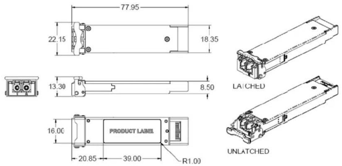
XFP Transceiver (dimensions are in mm)
X. PCB Layout and Bezel Recommendations
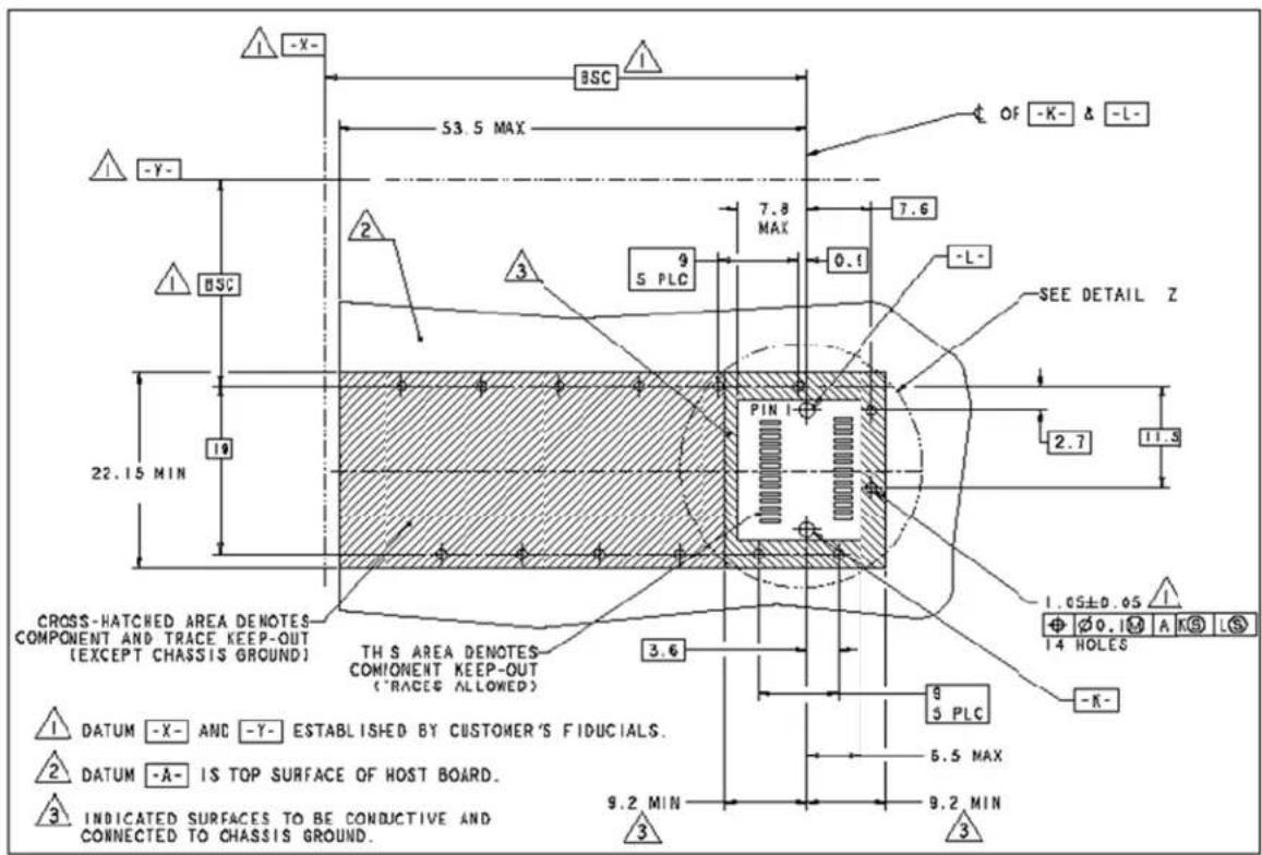
XFP Host Board Mechanical Layout (dimensions are in mm)
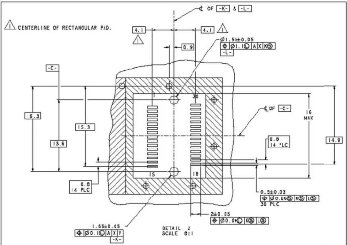
XFP Detail Host Board Mechanical Layout (dimensions are in mm)
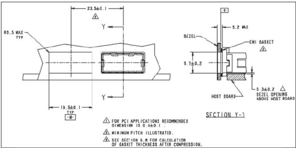
XFP Recommended Bezel Design (dimensions are in mm)
XI. References
- 10 Gigabit Small Form Factor Pluggable Module (XFP) Multi-Source Agreement (MSA), INF-8077i, Rev 4.5 – August 2005. Documentation is currently available at http://www.xfpmsa.org/
- Application Note AN-2035: “Digital Diagnostic Monitoring Interface for XFP Optical Transceivers” – Finisar Corporation, December 2003
- Directive 2002/95/EC of the European Council Parliament and of the Council, "on the restriction of the use of certain hazardous substances in electrical and electronic equipment". January 27, 2003.
- “Application Note AN-2038: Finisar Implementation Of RoHS Compliant Transceivers”, Finisar Corporation, January 21, 2005.
XII. For More Information
Finisar Corporation
1389 Moffett Park Drive
Sunnyvale, CA 94089-1133
Tel. 1-408-548-1000
Fax 1-408-541-6138
sales@finisar.com
www.finisar.com