
Creator TRX40 - Motherboard MSI - Free user manual and instructions
Find the device manual for free Creator TRX40 MSI in PDF.


| Product Type | Motherboard |
| Brand | MSI |
| Model | Creator TRX40 |
| Form Factor | E-ATX (12 in. x 10.9 in. / 30.4 cm x 27.7 cm) |
| CPU Support | 3rd Gen AMD Ryzen Threadripper Desktop Processors |
| Chipset | AMD TRX40 |
| Memory Support | 8x DDR4, up to 256GB, quad channel, up to 4666 MHz (1DPC 1R) |
| Expansion Slots | 4x PCIe 4.0 x16 (x16/x8/x16/x8) |
| Storage | 6x SATA 6Gb/s; 3x M.2 (PCIe 4.0 x4 & SATA), RAID 0/1/10 |
| LAN | 1x Intel I211AT Gigabit; 1x Aquantia AQC107 10-Gigabit |
| WiFi & Bluetooth | Intel Wi-Fi 6 AX200, Bluetooth 5 |
| USB Ports (Rear) | 5x USB 3.2 Gen2 Type-A; 4x USB 3.2 Gen1 Type-A; 1x USB 3.2 Gen2x2 Type-C |
| Audio | Realtek ALC1220 + ALC4050H, 7.1-channel HD Audio, S/PDIF out |
| Power Connectors | 1x 24-pin ATX, 2x 8-pin ATX 12V |
| Recommended PSU | 750W or higher |
| Cooling Features | FROZR heatsink design, Propeller Blade technology, extended heatpipe, pump fan support (up to 2A) |
| LED Lighting | Mystic Light, supports RGB (12V), ARGB (5V), and CORSAIR RGB |
| BIOS | 64 Mb UEFI AMI, Click BIOS 5, Flash BIOS Button |
| Software | Creator Center, Nahimic Audio, Live Update, etc. |
| Safety & Protection | DDR4 Steel Armor, M.2 Shield Frozr, PCI-E Steel Armor, ESD protection |
| Warranty | Check local distributor; typical 3 years |
| Repairability | User-replaceable CMOS battery, standard screws; M.2 and CPU socket protective caps required for RMA |
Frequently Asked Questions - Creator TRX40 MSI
User questions about Creator TRX40 MSI
0 question about this device. Answer the ones you know or ask your own.
Ask a new question about this device
Download the instructions for your Motherboard in PDF format for free! Find your manual Creator TRX40 - MSI and take your electronic device back in hand. On this page are published all the documents necessary for the use of your device. Creator TRX40 by MSI.
USER MANUAL Creator TRX40 MSI
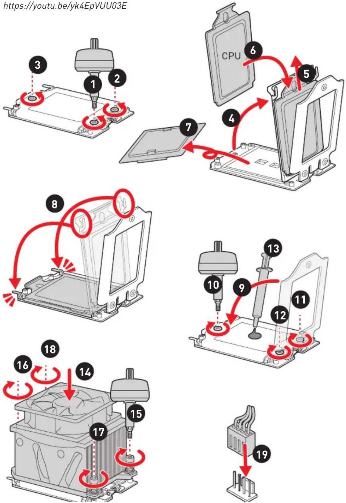
Thank you for purchasing the MSI® Creator TRX40 motherboard. This Quick Start section provides demonstration diagrams about how to install your computer. Some of the installations also provide video demonstrations. Please link to the URL to watch it with the web browser on your phone or tablet. You may have even link to the URL by scanning the QR code.
クイックスタート
优酷

http://v.youku.
com/v_show/id
XMjk4NzgxOTQ4NA==.
html
https://youtu.be/yk4EpVUU03E
flowchart
graph TD
    A["1: Computer with CPU"] --> B["2: Screwdriver"]
    B --> C["3: Screwdriver with CPU"]
    C --> D["4: Screwdriver with CPU"]
    D --> E["5: Screwdriver with CPU"]
    E --> F["6: CPU with CPU"]
    F --> G["7: Computer with CPU"]
    G --> H["8: Screwdriver with CPU"]
    H --> I["9: Screwdriver with CPU"]
    I --> J["10: Screwdriver with CPU"]
    J --> K["11: Screwdriver with CPU"]
    K --> L["12: Screwdriver with CPU"]
    L --> M["13: Screwdriver with CPU"]
    M --> N["14: Screwdriver with CPU"]
    N --> O["15: Screwdriver with CPU"]
    O --> P["16: Screwdriver with CPU"]
    P --> Q["17: Screwdriver with CPU"]
    Q --> R["18: Screwdriver with CPU"]
    R --> S["19: Screwdriver with CPU"]
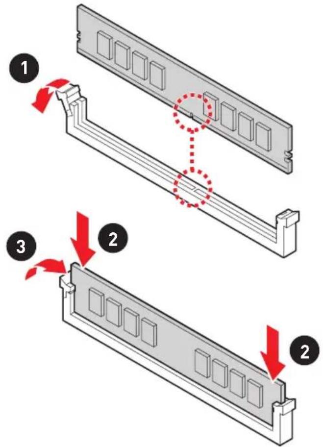
Installing DDR4 memory/ DDR4メモリの取り付け/ DDR4 メ모리 설치하기/ 安装 DDR4 記憶體/ 安装 DDR4 内存
Youtube

优酷

http://youtu.be/T03aDrJPyQs
http://v.youku.com/v_show/id_XNzUyMTI50DI4.html
| D2 D1 C2 C1 CPU A1 A2 B1 B2 | |||||||||
| 1 DIMM | 3rd Gen AMD RyzenTM ThreadripperTM Desktop Processors | √ | |||||||
| 2 DIMMs | √ | √ | |||||||
| 4 DIMMs | √ | √ | √ | √ | |||||
| 8 DIMMs | √ | √ | √ | √ | √ | √ | √ | √ | |
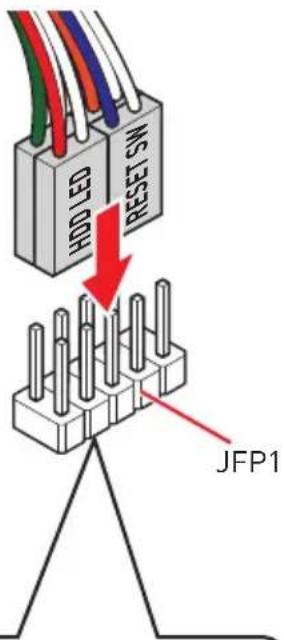
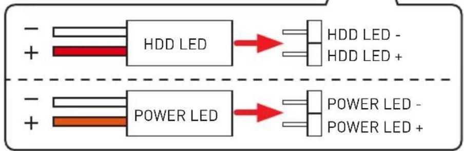
Connecting the Front Panel Header/
flowchart
graph LR
    A["+ - HDD LED"] --> B["HD- HDD LED"]
    C["+ - POWER LED"] --> D["HD- POWER LED"]
    E["+ - Power LED"] --> F["HD- POWER LED"]
    G["+ - Power LED"] --> H["HD- POWER LED"]
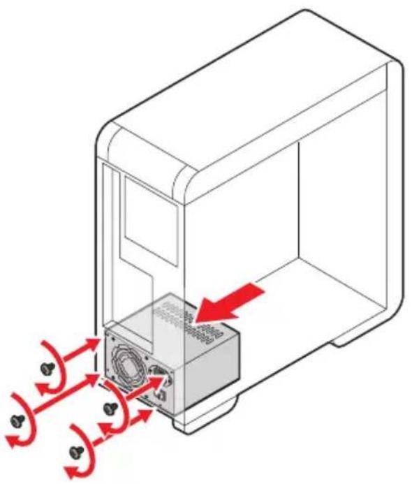
Connecting the Power Connectors/ 電源コネクターの接続/ 전원 커넥터 연결하기/ 插上電源接頭/ 连接电源接头
Youtube

优酷

http://youtu.be/gkDYyR_83I4 http://v.youku.com/v_show/id_XNDkzODU0MDQw.html
natural_image
Diagram of a device interior with red arrows indicating airflow or movement, showing internal components and directional arrows (no text or symbols)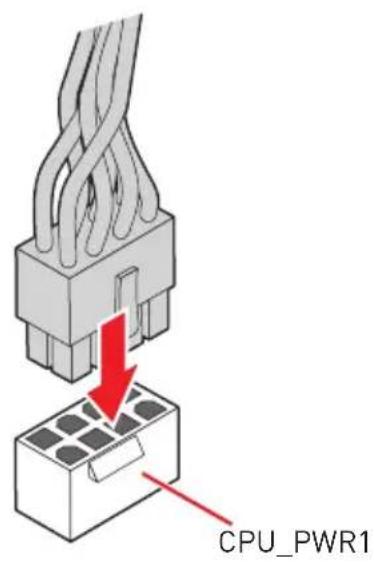
http://v.youku.com/v_show/id_XNDkzODU5MTky.html
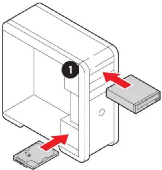
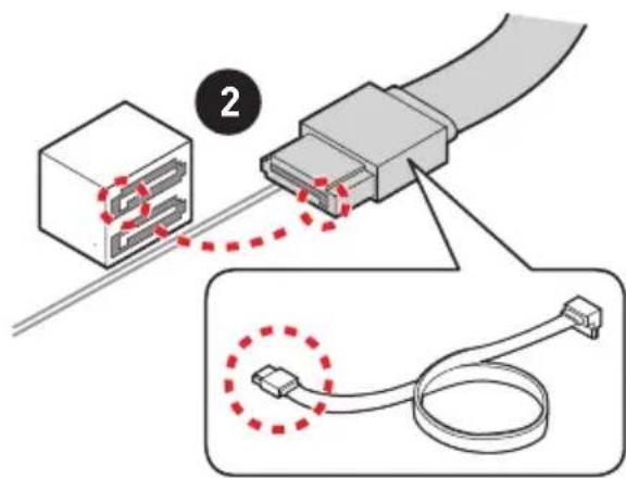
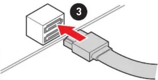
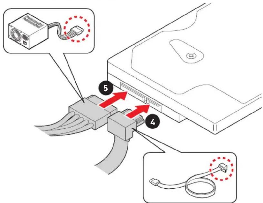
http://youtu.be/mG0GZpr9w_A
优酷

http://v.youku.com/v_show/id_XNDkyOTc3MzQ4.html
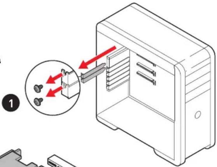
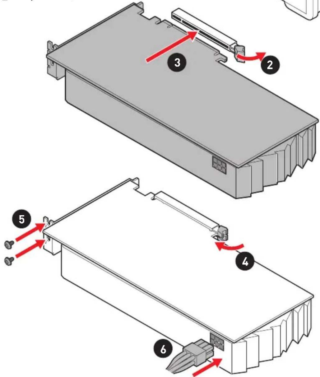
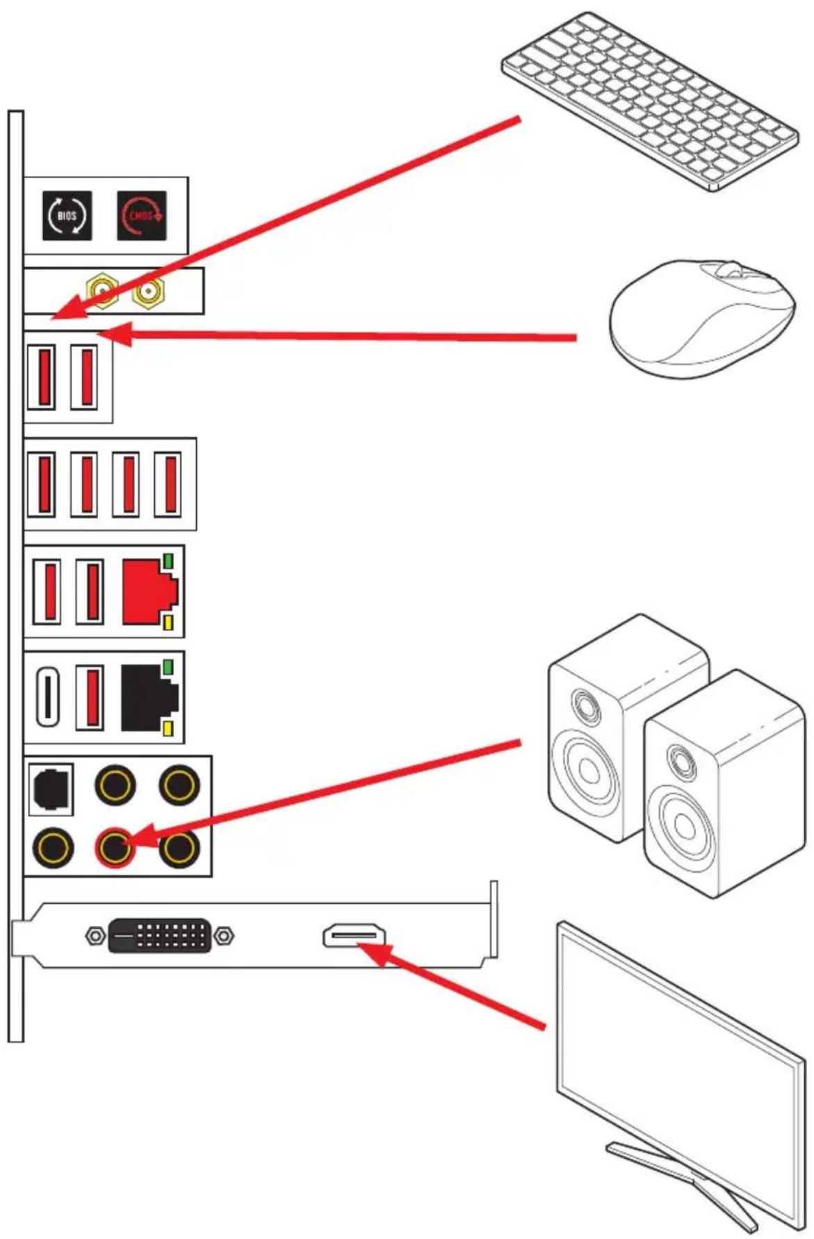
Connecting Peripheral Devices/ 周辺機器の接続/ 주변 장치 연결하기/ 連接周邊設備/ 连接外围设备
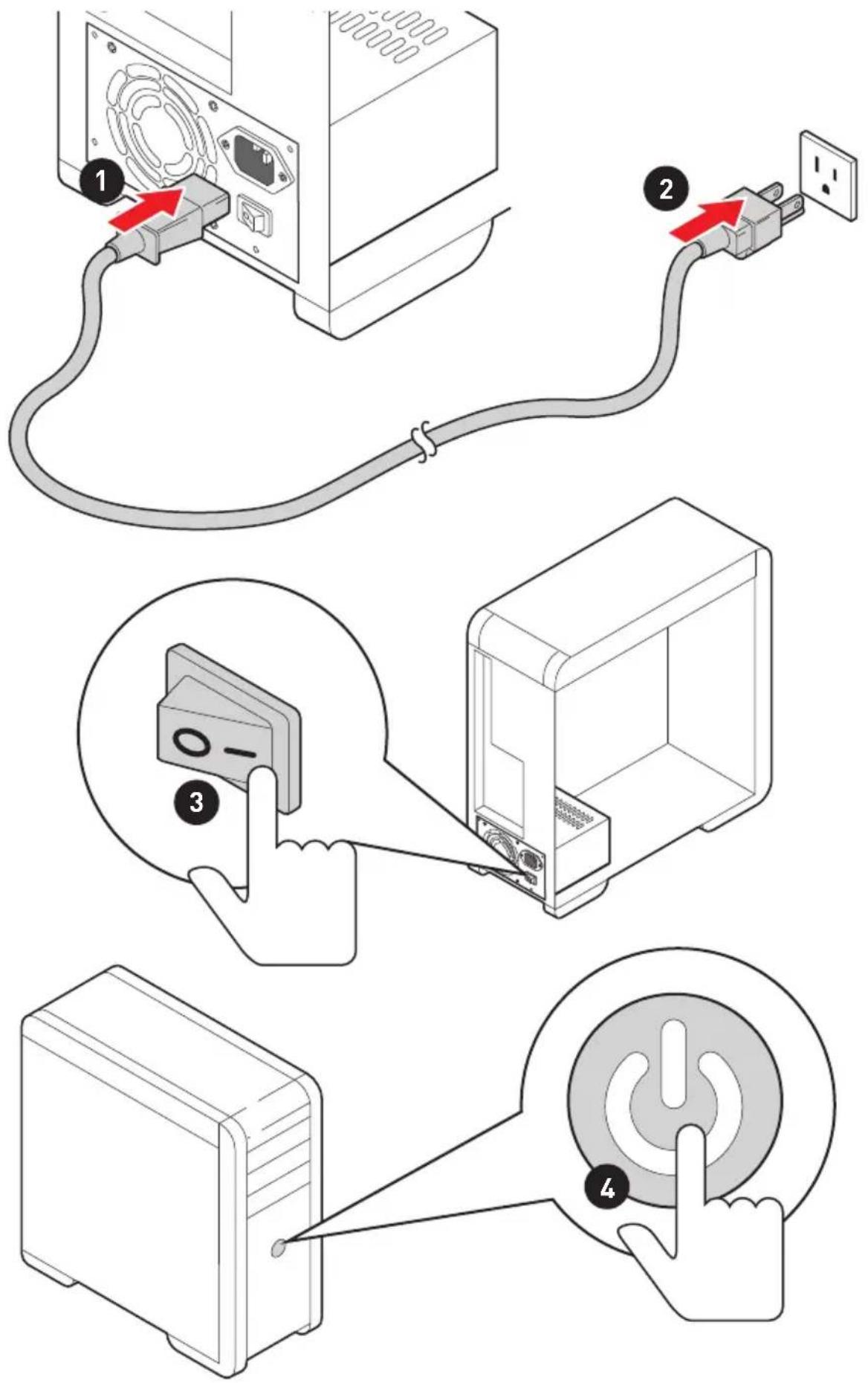
Power On/通電/전원 켜기/啟動電源/开机
Contents
Safety Information....3
Specifications....4
JCORSAIR1 Connector Specification....9
Package contents 10
Rear I/O Panel 11
LAN Port LED Status Table 11
Audio Ports Configuration....11
Realtek Audio Console 12
Installing Antennas.... 14
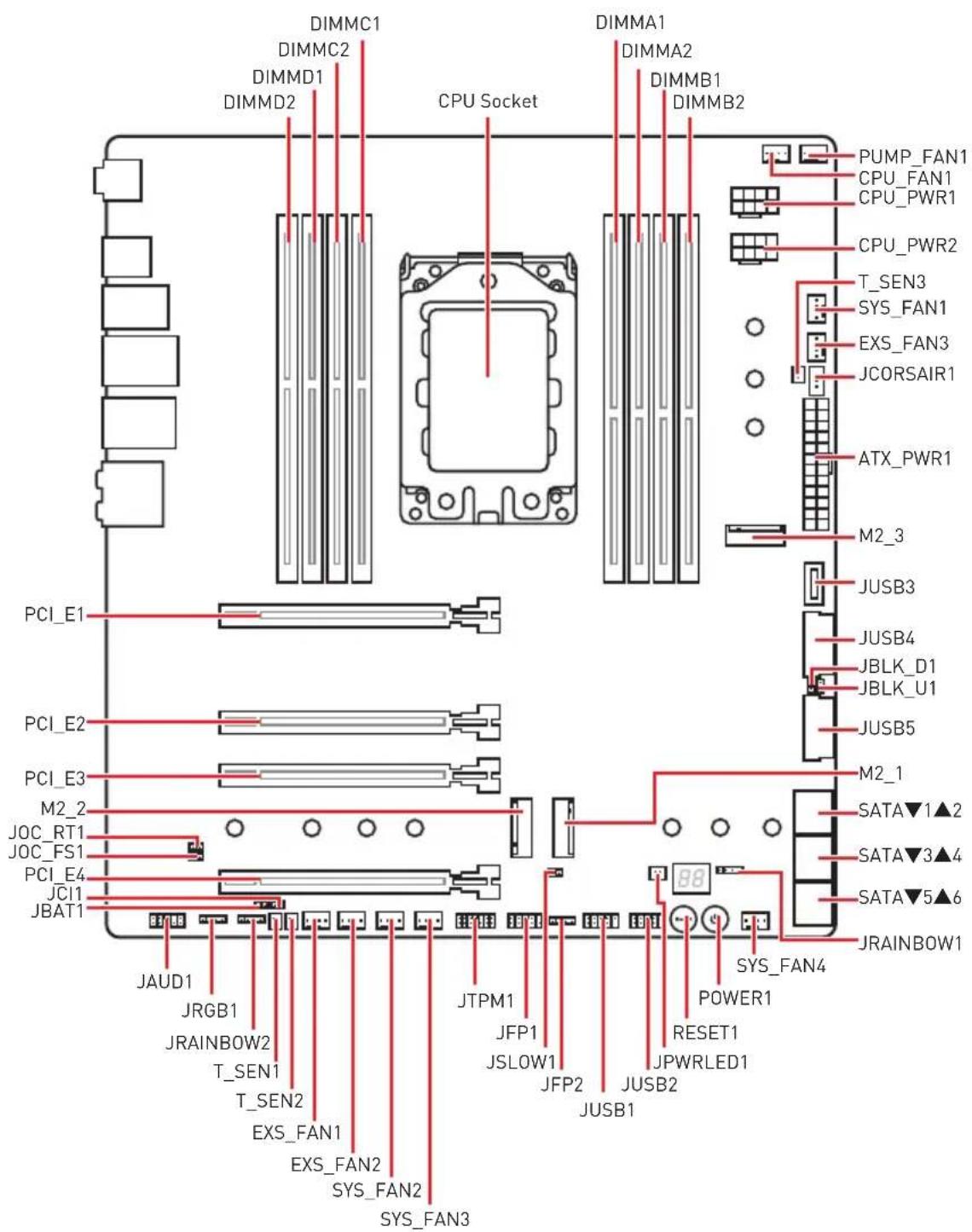
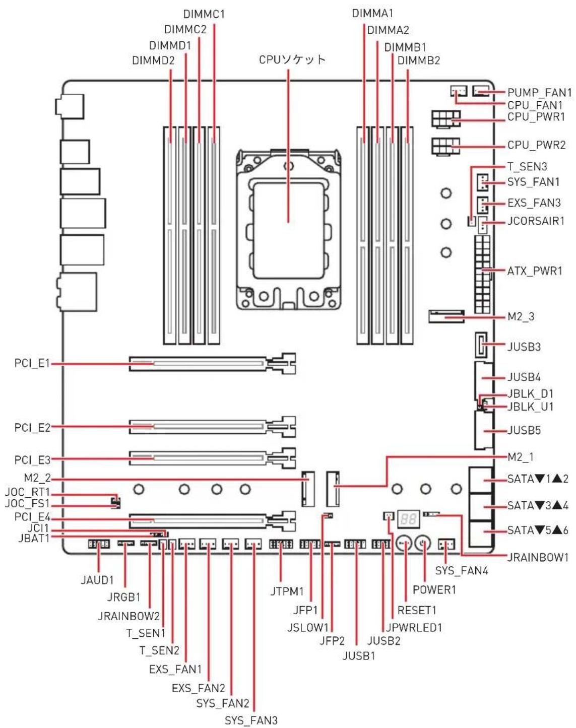
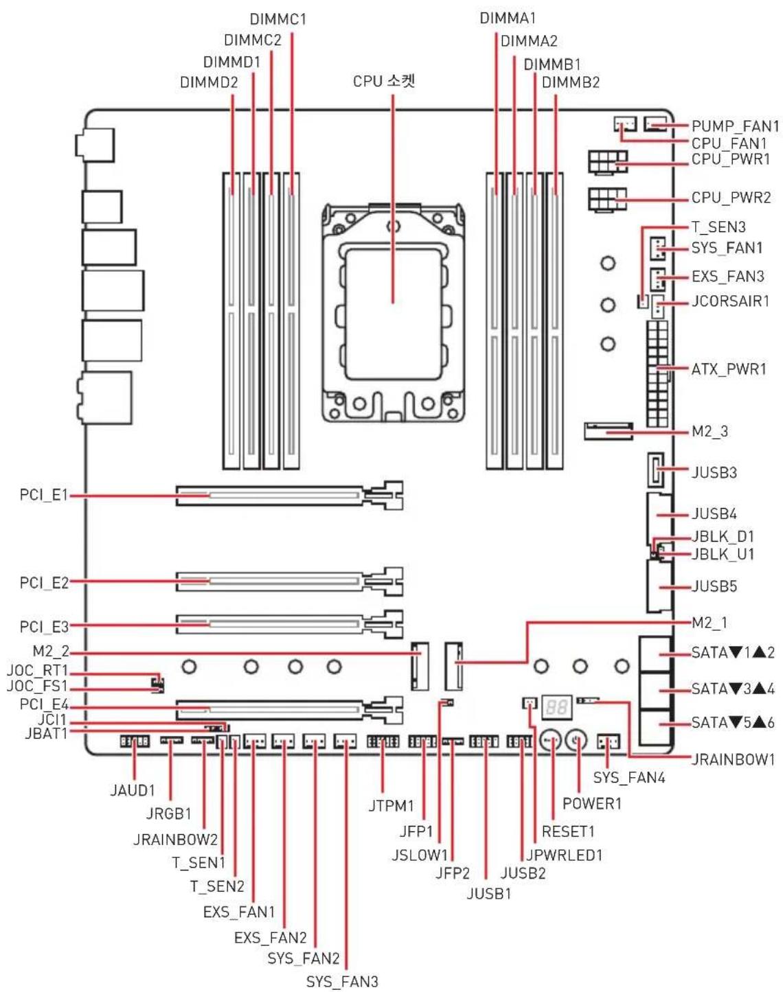
Overview of Components 15
CPU Socket 16
DIMM Slots.... 19
PCI_E1\~4: PCIe Expansion Slots 21
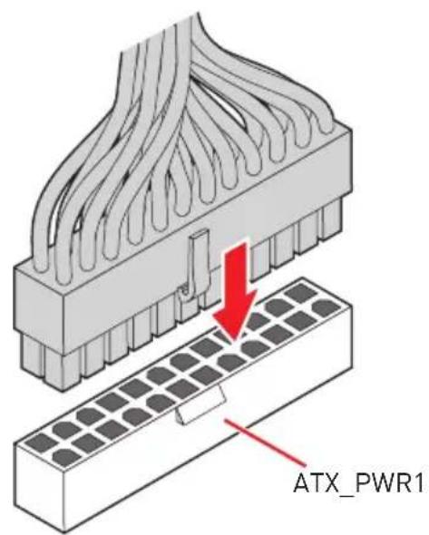
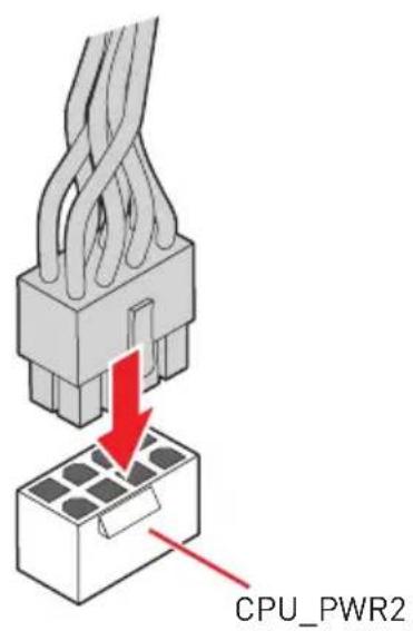
CPU_PWR1\~2, ATX_PWR1: Power Connectors.... 23
M2_1\~3: M.2 Slots (Key M) 24
Installing M.2 XPANDER-AERO GEN4.... 26
SATA1\~6: SATA 6Gb/s Connectors....28
JFP1, JFP2: Front Panel Connectors.... 28
JUSB1\~2: USB 2.0 Connectors....29
JUSB3: USB 3.2 Gen2 Type-C Connector.... 29
JUSB4\~5: USB 3.2 Gen1 Connectors .... 30
JAUD1: Front Audio Connector 30
CPU_FAN1, PUMP_FAN1, SYS_FAN1\~4, EXS_FAN1\~3,: Fan Connectors...... 31
T_SEN1\~3: Thermal Sensor Connectors 32
JBLK_D1, JBLK_U1: Base Clock Down & Up Header 32
POWER1, RESET1: Power Button, Reset Button 32
JTPM1: TPM Module Connector....33
JBAT1: Clear CMOS (Reset BIOS) Jumper 33
JCI1: Chassis Intrusion Connector 34
JRGB1: RGB LED connector 35
JRAINBOW1\~2: Addressable RGB LED connectors 36
JCORSAIR1: CORSAIR Connector 37
JOC_RT1: OC Retry Button.... 38
JOC_FS1: OC Force Enter BIOS Button 38
JSLOW1: Slow Mode Booting Jumper 38
Onboard LEDs....39
EZ Debug LED 39
JPWRLED1: LED power input....39
Debug Code LED 40
Hexadecimal Character Table....40
Boot Phases....40
Debug Code LED Table....40
ACPI States Codes 44
Installing OS, Drivers & Utilities 45
Installing Windows ^® 10....45
Installing Drivers 45
Installing Utilities 45
BIOS Setup 46
Entering BIOS Setup....46
Resetting BIOS....47
Updating BIOS....47
EZ Mode 49
Advanced Mode 51
OC Menu....52
Safety Information
- The components included in this package are prone to damage from electrostatic discharge (ESD). Please adhere to the following instructions to ensure successful computer assembly.
- Ensure that all components are securely connected. Loose connections may cause the computer to not recognize a component or fail to start.
- Hold the motherboard by the edges to avoid touching sensitive components.
- It is recommended to wear an electrostatic discharge (ESD) wrist strap when handling the motherboard to prevent electrostatic damage. If an ESD wrist strap is not available, discharge yourself of static electricity by touching another metal object before handling the motherboard.
- Store the motherboard in an electrostatic shielding container or on an anti-static pad whenever the motherboard is not installed.
- Before turning on the computer, ensure that there are no loose screws or metal components on the motherboard or anywhere within the computer case.
- Do not boot the computer before installation is completed. This could cause permanent damage to the components as well as injury to the user.
- If you need help during any installation step, please consult a certified computer technician.
- Always turn off the power supply and unplug the power cord from the power outlet before installing or removing any computer component.
- Keep this user guide for future reference.
- Keep this motherboard away from humidity.
- Make sure that your electrical outlet provides the same voltage as is indicated on the PSU, before connecting the PSU to the electrical outlet.
- Place the power cord such a way that people can not step on it. Do not place anything over the power cord.
- All cautions and warnings on the motherboard should be noted.
- If any of the following situations arises, get the motherboard checked by service personnel:
- Liquid has penetrated into the computer.
■ The motherboard has been exposed to moisture.
- The motherboard does not work well or you can not get it work according to user guide.
■ The motherboard has been dropped and damaged.
■ The motherboard has obvious sign of breakage.
- Do not leave this motherboard in an environment above 60^ (140°F), it may damage the motherboard.
Specifications
| CPU supports 3rd Gen AMD RyzenTM ThreadripperTM Desktop Processors | |
| Chipset AMD® TRX40 Chipset | |
| Memory | 8x DDR4 memory slots, support up to 256GB*Supports JEDEC 1R 2133/ 2400/ 2666/ 3200 MHz1DPC 1R max speed 4666 MHz1DPC 2R max speed 4000 MHz2DPC 1R max speed 3866 MHz2DPC 2R max speed 3466 MHzQuad channel memory architecture**Supports non-ECC UDIMM memorySupports ECC UDIMM memorySupports un-buffered memory* For the latest information about memory, please visit http://www.msi.com** Please refer the DIMM Slots section for more details. |
| Expansion Slot 4x PCIe 4.0 x16 slots (support x16/x8/x16/x8 mode) | |
| Multi-GPU | Supports 3-Way NVIDIA® SLITM TechnologySupports 3-Way AMD® CrossFireTM Technology |
| Storage | AMD® TRX40 Chipset6x SATA 6Gb/s ports1x M.2 slot (M2_3, Key M)Supports PCIe 4.0 x4 and SATA 6Gb/s 2242/ 2260 /2280 storage devices3rd Gen AMD RyzenTM ThreadripperTM Desktop Processor2x M.2 slots (M2_1 & M2_2, Key M)M2_1 supports PCIe 4.0 x4 and SATA 6Gb/s 2242/ 2260 /2280 storage devicesM2_2 supports PCIe 4.0 x4 and SATA 6Gb/s 2242/ 2260 /2280/ 22110 storage devices |
| RAID | AMD® TRX40 ChipsetSupports RAID 0, RAID 1 and RAID 10 |
| LAN | 1x Intel® I211AT Gigabit LAN controller1x Aquantia® AQC107 10-Gigabit LAN controller |
Continued on next page
Continued from previous page
| WiFi & Bluetooth | Intel®Wi-Fi 6 AX200The Wireless module is pre-install in the M2_4 (Key-E) slotSupports 802.11 a/b/g/n/ac/ax, MU-MINO Rx, 2.4GHz-5GHz (160MHz) up to 2.4GbpsSupports Bluetooth®5 |
| USB | AMD®TRX40 Chipset2x USB 3.2 Gen2 (SuperSpeed USB 10Gbps) ports (1 Type-A port on the back panel and 1 Type-C port through the internal USB connector)8x USB 3.2 Gen1 (SuperSpeed USB) ports (4 Type-A ports on the back panel, 4 ports available through the internal USB 3.2 Gen1 connectors)4x USB 2.0 (High-speed USB) ports available through the internal USB 2.0 connectors3rd Gen AMD RyzenTM ThreadripperTM Desktop Processor4x USB 3.2 Gen2 (SuperSpeed USB 10Gbps) Type-A ports on the back panelASMedia®ASM3242 Chipset1x USB 3.2 Gen2x2 (SuperSpeed USB 20Gbps) Type-port on the back panel |
| Audio | 1x Realtek®ALC1220 Codec7.1-Channel High Definition Audio1x Realtek®ALC4050H CodecSupports front & rear panel Mic-inSupports S/PDIF output |
| Back Panel Connectors | 1x Clear CMOS button1x Flash BIOS Button2x Wi-Fi Antenna connectors5x USB 3.2 Gen2 Type-A ports1x Flash BIOS Port4x USB 3.2 Gen1 Type-A ports1x USB 3.2 Gen2x2 Type-C port2x LAN (RJ45) ports5x OFC audio jacks1x Optical S/PDIF OUT connector |
Continued on next page
Continued from previous page
| Internal Connectors | 1x 24-pin ATX main power connector2x 8-pin ATX 12V power connectors6x SATA 6Gb/s connectors3x M.2 slots (M-Key)1x USB 3.2 Gen2 Type-C port2x USB 3.2 Gen1 connectors (supports additional 4 USB 3.2 Gen1 ports)2x USB 2.0 connectors (supports additional 4 USB 2.0 ports)1x 4-pin CPU fan connector1x 4-pin pump fan connector (supports up to 2A)4x 4-pin system fan connectors3x 4-pin extend fan connectors1x Front panel audio connector2x System panel connectors1x Chassis Intrusion connector1x TPM module connector3x 2-pin Thermal Sensors connectors1x 4-pin 5050 RGB LED connector2x 3-pin ARGB LED connectors1x 3-pin CORSAIR LED connector1x LED demo connector1x JBLK_U pin header1x JBLK_D pin header1x OC retry pin header1x OC force enter pin header1x Slow mode booting jumper |
| Internal Buttons | 1x Power button1x Reset button |
| Debug LED | 1x 2-Digit Debug Code LED4x EZ Debug LED |
| I/O Controller NUVOTON NCT6797 Controller Chip | |
Continued on next page
Continued from previous page
| Hardware Monitor | CPU/System/Chipset temperature detectionCPU/System/Chipset fan speed detectionCPU/System/Chipset fan speed control |
| Form Factor | E-ATX Form Factor12 in. x 10.9 in. (30.4 cm x 27.7 cm) |
| BIOS Features | 1x 64 Mb flashUEFI AMI BIOSACPI 6.1, SMBIOS 2.8Multi-language |
| Software | DriversCREATOR CENTERNahimic AudioCPU-Z MSI GAMINGMSI App Player (BlueStacks)Open Broadcaster Software (OBS)Google ChromeTM, Google Toolbar, Google DriveNortonTM Internet Security Solution |
| Creator Center Features | Creator OptimizationCreator HotkeyMystic LightHardware MonitorTrue ColorLive UpdateSpeed UpSmart ToolSuper Charger  Please refer to http://download.msi.com/manual/mb/CREATORCENTER.pdf for more details. Please refer to http://download.msi.com/manual/mb/CREATORCENTER.pdf for more details. |
Continued on next page
Continued from previous page
| Special Features | AudioAudio Boost 4Nahimic 3Voice BoostNetwork10G SUPER LANLAN ManagerDual LANIntel WiFiStorageLightning Gen4 M.2CoolingFROZR Heastink DesignPropeller Blade technologyExtended Hipe-pipe DesignPump FanFan ControlLEDMystic LightMystic Light Extension (RGB)Mystic Light Extension (RAINBOW)Mystic Light Extension (CORSAIR)Mystic Light SyncAmbient LinkEZ DEBUG LEDProtectionDDR4 Steel ArmorM.2 Shield FrozrPCI-E Steel ArmorPre-installed IO shielding |
Continued on next page
Continued from previous page
| Special Features | PerformanceLightning Gen 4 PCI-E SlotMulti GPU - SLI TechnologyMulti GPU - CrossFire TechnologyDDR4 BoostCore BoostOC Engine(Clock gen)USB with type A+CAMD Turbo USB 3.2 Gen 2Lightning USB 20GDual CPU PowerUser ExperienceCreator CenterCreator HotkeySpeed UpTotal Fan ControlLive UpdateAPP PlayerBIOSClick BIOS 5Flash BIOS Button |
JCORSAIR1 Connector Specification
| Supporting CORSAIR RGB Products Maximum connection | |
| Lighting Node PRO LED Strip | 20* * 20% brightness is recommended when the number of LED strips exceeds 8. |
| HD120 RGB Fan 6 | |
| SP120 RGB Fan 6 | |
| LL120 RGB Fan 6 | |
Package contents
Please check the contents of your motherboard package. It should contain:
| Motherboard Creator | TRX40 | |
| Documentation | User manual 1 | |
| Quick installation guide 1 | ||
| Application USB drive with drivers & utilities 1 | ||
| Cables | SATA 6G cable 4 | |
| LED JRGB Y cable 1 | ||
| LED JCORSAIR cable 1 | ||
| LED JRAINBOW cable 1 | ||
| Thermal sensor cable 3 | ||
| Expansion card M.2 XPANDER-AERO GEN4 1 | ||
| Accessories | Wi-Fi antenna 1 | |
| Case badge 1 | ||
| SATA cable stickers 1 | ||
| Product registration card 1 | ||
| M.2 screws 3 | ||

Important
If any of the above items are damaged or missing, please contact your retailer.
Rear I/O Panel
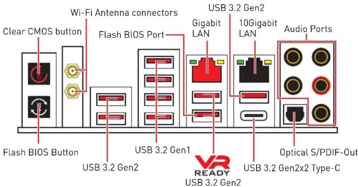
- Clear CMOS button - Power off your computer. Press and hold the Clear CMOS button for about 5-10 seconds to reset BIOS to default values.
- Flash BIOS Button/Port - Please refer to page 48 for Updating BIOS with Flash BIOS Button.
LAN Port LED Status Table
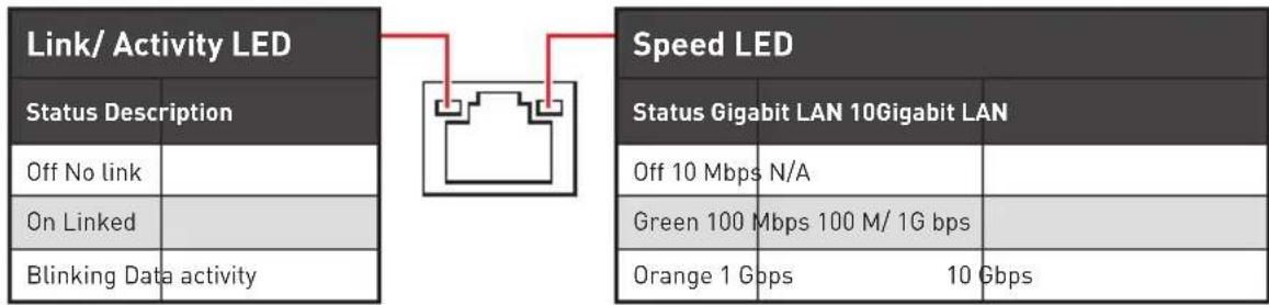
flowchart
graph LR
    A["Link/ Activity LED"] --> B["Speed LED"]
    C["Status Description"] --> A
    D["Off No link"] --> A
    E["On Linked"] --> A
    F["Blinking Data activity"] --> A
    G["Off 10 Mbps N/A"] --> A
    H["Green 100 Mbps 100 M/ 1G bps"] --> A
    I["Orange 1 Gbps 10 Gbps"] --> A
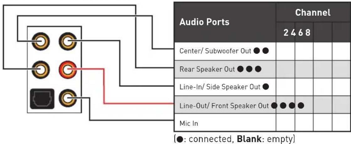
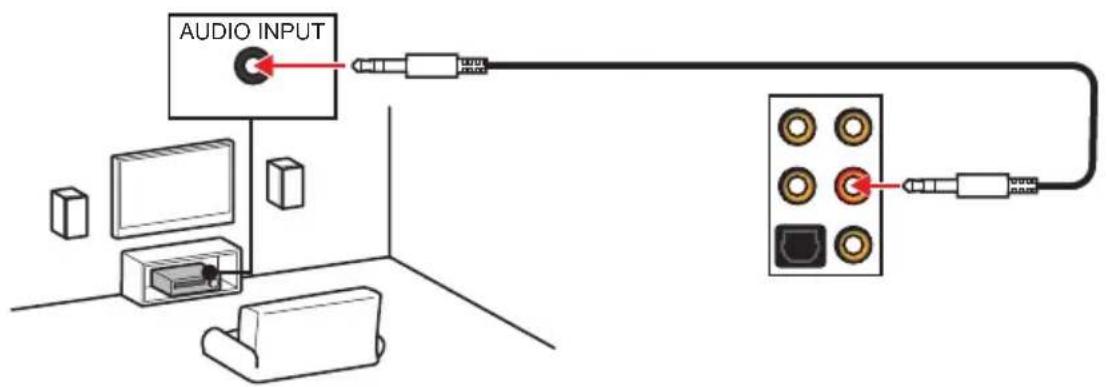
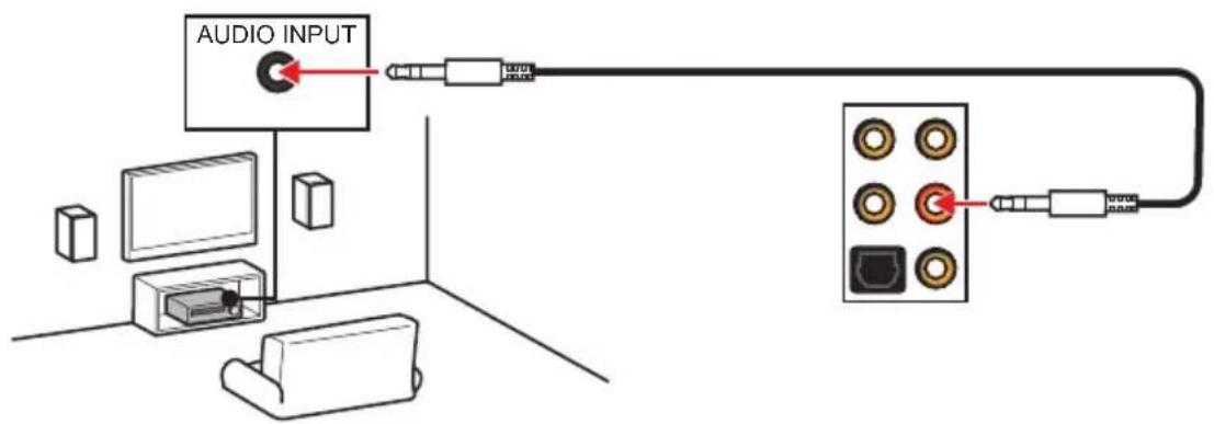
Audio Ports Configuration
Realtek Audio Console
After Realtek Audio Console is installed. You can use it to change sound settings to get better sound experience.
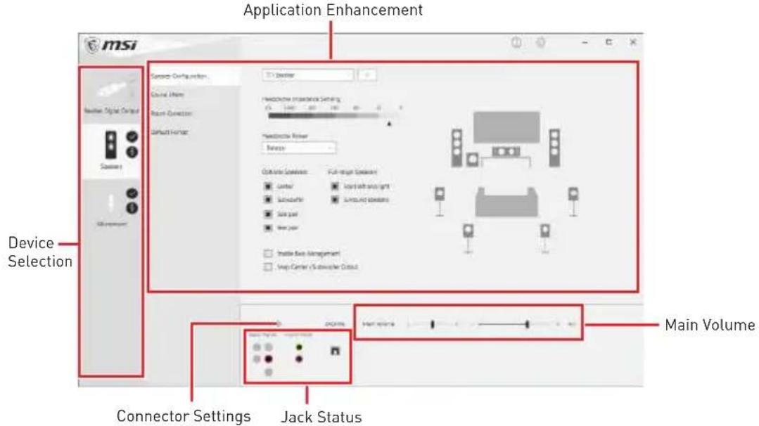
- Device Selection - allows you to select a audio output source to change the related options. The check sign indicates the devices as default.
- Application Enhancement - the array of options will provide you a complete guidance of anticipated sound effect for both output and input device.
- Main Volume - controls the volume or balance the right/left side of the speakers that you plugged in front or rear panel by adjust the bar.
- Jack Status - depicts all render and capture devices currently connected with your computer.
- Connector Settings - configures the connection settings.
Auto popup dialog
When you plug into a device at an audio jack, a dialogue window will pop up asking you which device is current connected.
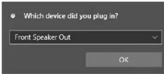
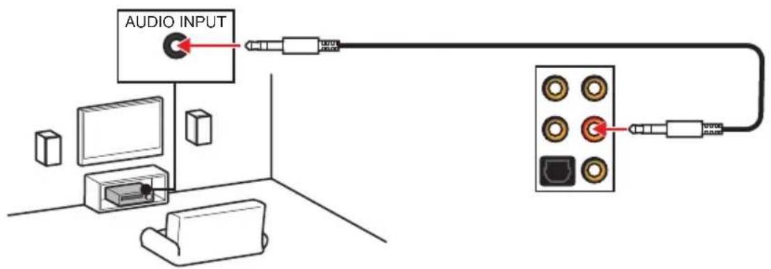
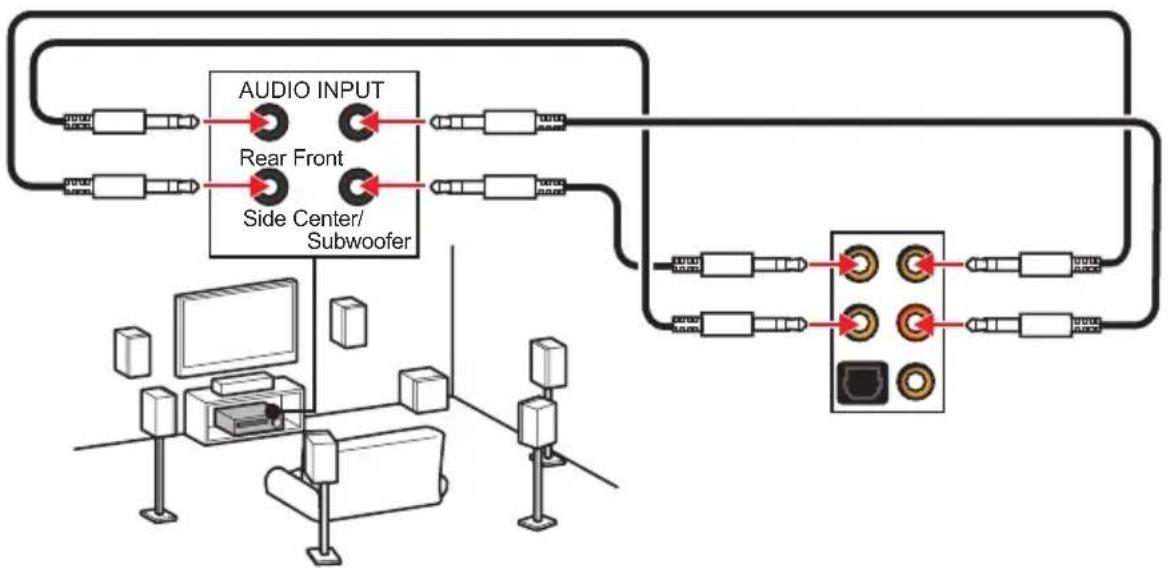
Each jack corresponds to its default setting as shown on the next page.

The pictures above for reference only and may vary from the product you purchased.
Audio jacks to headphone and microphone diagram
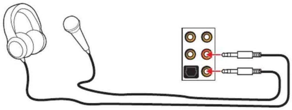
natural_image
Diagram showing a headset connected to an audio jack via a cable, with no text or symbols present.Audio jacks to stereo speakers diagram
Audio jacks to 7.1-channel speakers diagram
flowchart
graph TD
    A["Audio Input"] --> B["Rear Front"]
    B --> C["Side Center/Subwoofer"]
    C --> D["Output Module 1"]
    C --> E["Output Module 2"]
    C --> F["Output Module 3"]
    C --> G["Output Module 4"]
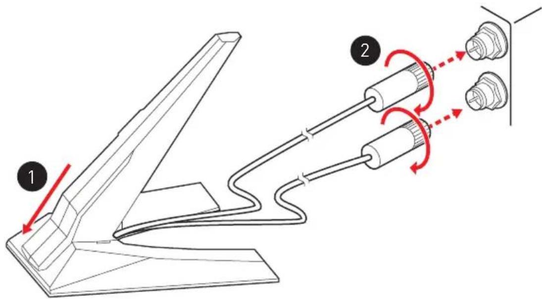
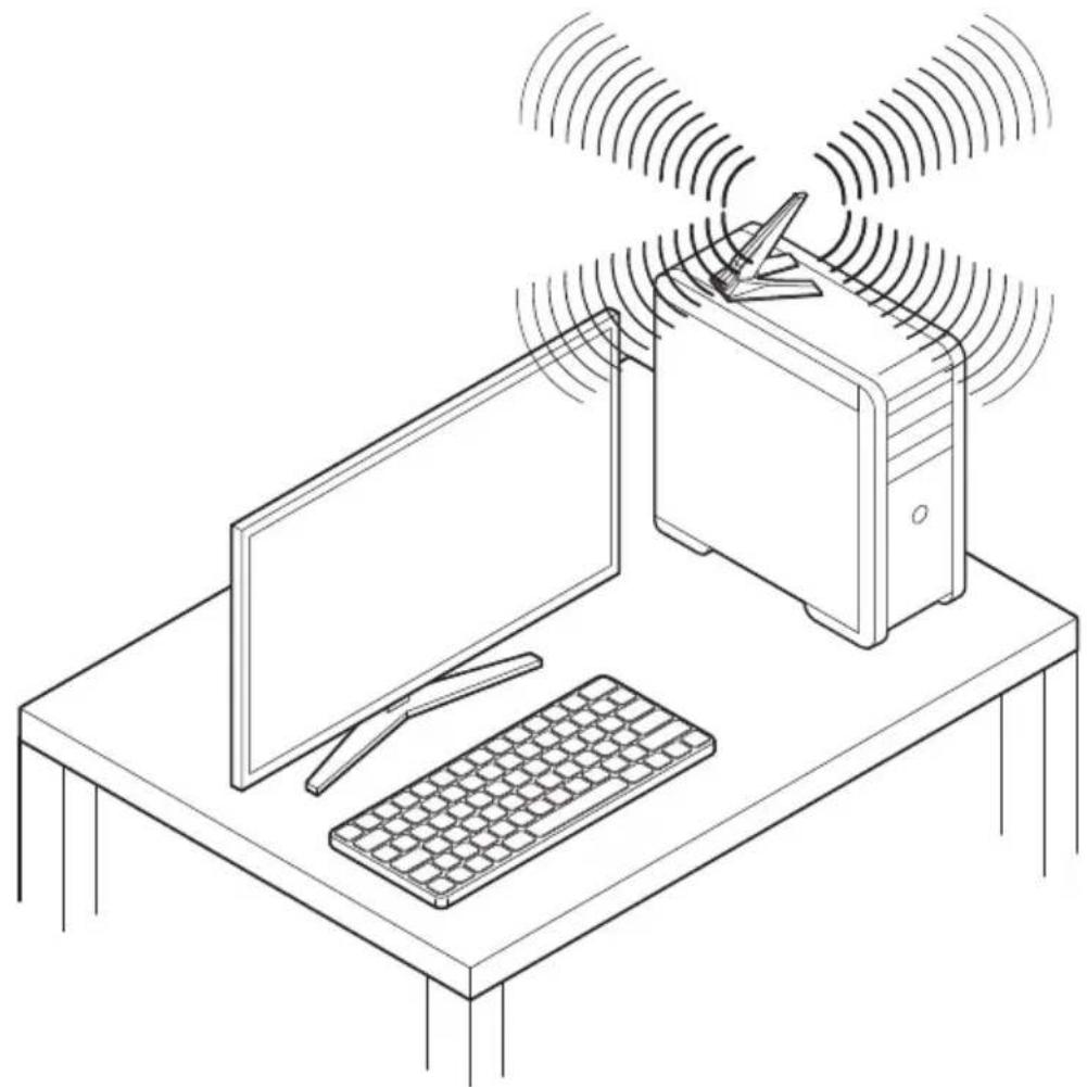
Installing Antennas
-
Combine the antenna with the base.
-
Screw two antenna cables tight to the WiFi antenna connectors as shown.
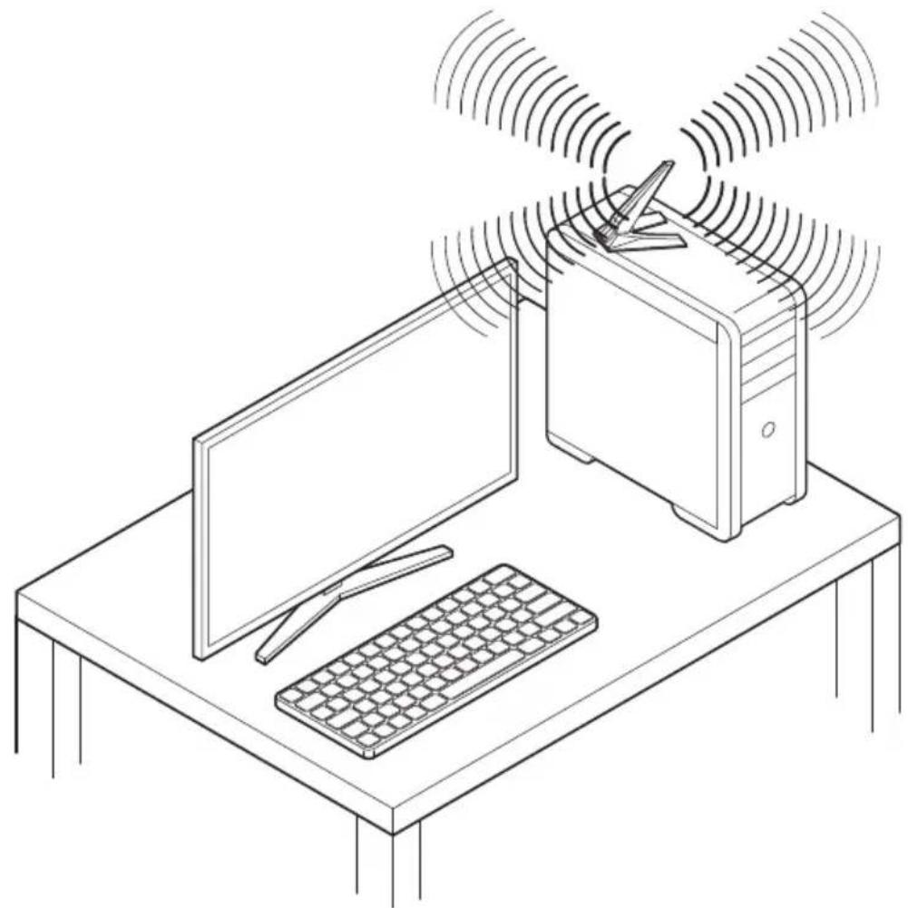
- Place the antenna as high as possible.
natural_image
Isometric line drawing of a desktop computer setup with monitor, keyboard, tower, and wireless signal waves (no text or symbols)Overview of Components
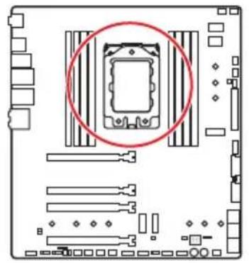
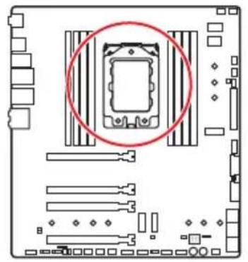
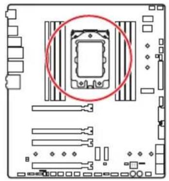
CPU Socket
natural_image
Diagram of a computer motherboard showing slots, connectors, and a highlighted component (no text or labels)Distance from the center of the CPU to the nearest DIMM slot.
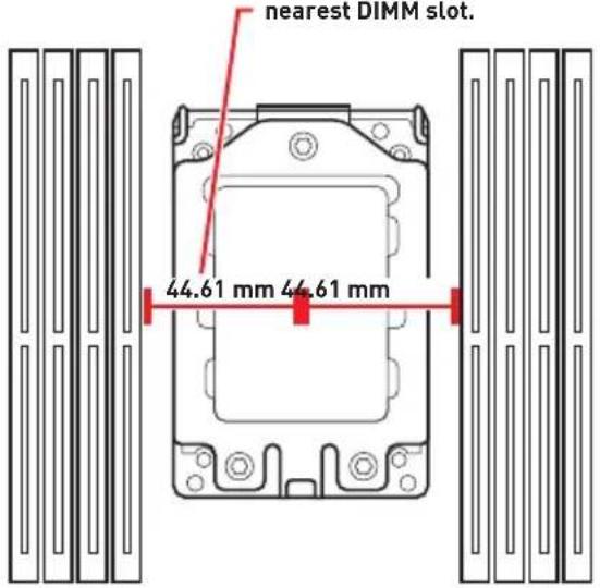


Demonstration
Watch the video to learn how to unbox and install AMD Ryzen Threadripper CPU.
https://youtu.be/yk4EpVUU03E
Please use the Torx screwdriver come with the AMD CPU and follow the steps below to install the CPU.
- Loosen load plate screws with the AMD Torx screwdriver in the sequence 3→2→1. The load plate will automatically lift up to the fully open position.
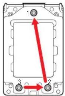
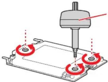
natural_image
Mechanical assembly diagram showing a turning tool interacting with two circular components (no text or symbols present)AMD Torx screwdriver
- Slide out the External Cap from the frame rail, and then slide the Carrier Frame with CPU into the frame rail. Make sure that the Carrier Frame with CPU has been properly installed in the frame rail.
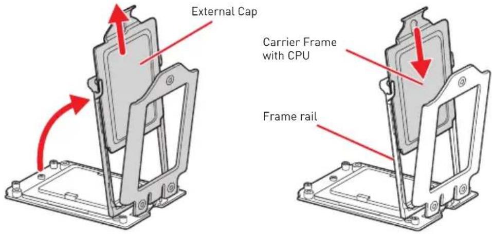
- Remove the protective pin cap, and then close and buckle the frame rail.
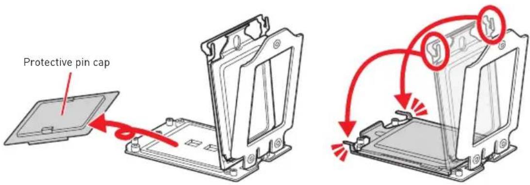
- Close the load plate, and then turn the load plate screws clockwise a little with the AMD Torx screwdriver in the sequence 1 2 3 1 2 3 until they are snug.
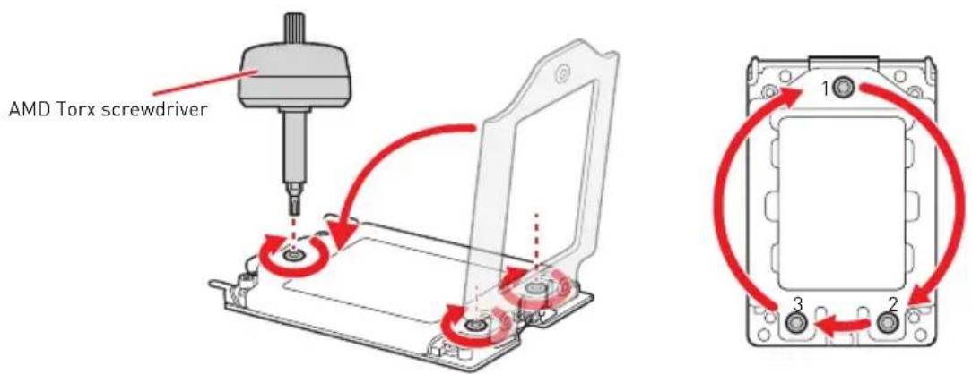
- Tighten load plate screws until you hear a click from the AMD Torx screwdriver.

If the load plate is not secured properly, the computer will not power on.
- Apply thermal paste on the top of the CPU.
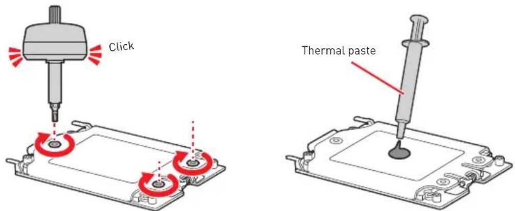
-
Place the heatsink on the motherboard, align the bolts with the mounting nuts on the motherboard. Then, tighten the bolts in a diagonal order to spread the tension properly across the sides.
-
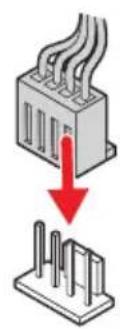
Finally, attach the CPU fan cable to the CPU fan connector on the motherboard.
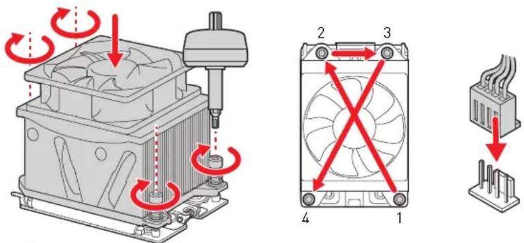

Always unplug the power cord from the power outlet before installing or removing the CPU.
Please retain the protective caps after installing the processor. MSI will deal with Return Merchandise Authorization (RMA) requests if only the motherboard comes with the protective caps on the CPU socket.
When installing a CPU, always remember to install a CPU heatsink. A CPU heatsink is necessary to prevent overheating and maintain system stability.
Confirm that the CPU heatsink has formed a tight seal with the CPU before booting your system.
Overheating can seriously damage the CPU and motherboard. Always make sure the cooling fans work properly to protect the CPU from overheating. Be sure to apply an even layer of thermal paste (or thermal tape) between the CPU and the heatsink to enhance heat dissipation.
Whenever the CPU is not installed, always protect the CPU socket pins by covering the socket with the plastic cap.
If you purchased a separate CPU and heatsink/ cooler, Please refer to the documentation in the heatsink/ cooler package for more details about installation.
This motherboard is designed to support overclocking. Before attempting to overclock, please make sure that all other system components can tolerate overclocking. Any attempt to operate beyond product specifications is not recommended. MSI® does not guarantee the damages or risks caused by inadequate operation beyond product specifications.
DIMM Slots
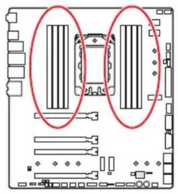
natural_image
Diagram of a computer motherboard showing two rows of slots and connectors (no text or labels)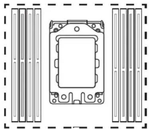
natural_image
Technical line drawing of a mechanical component with mounting holes and internal cavity, enclosed in a dashed border (no text or symbols)D2 D1 C2 C1 A1 A2 B1 B2
Memory module installation recommendation
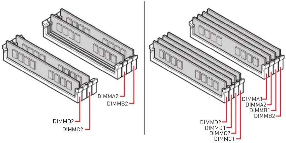
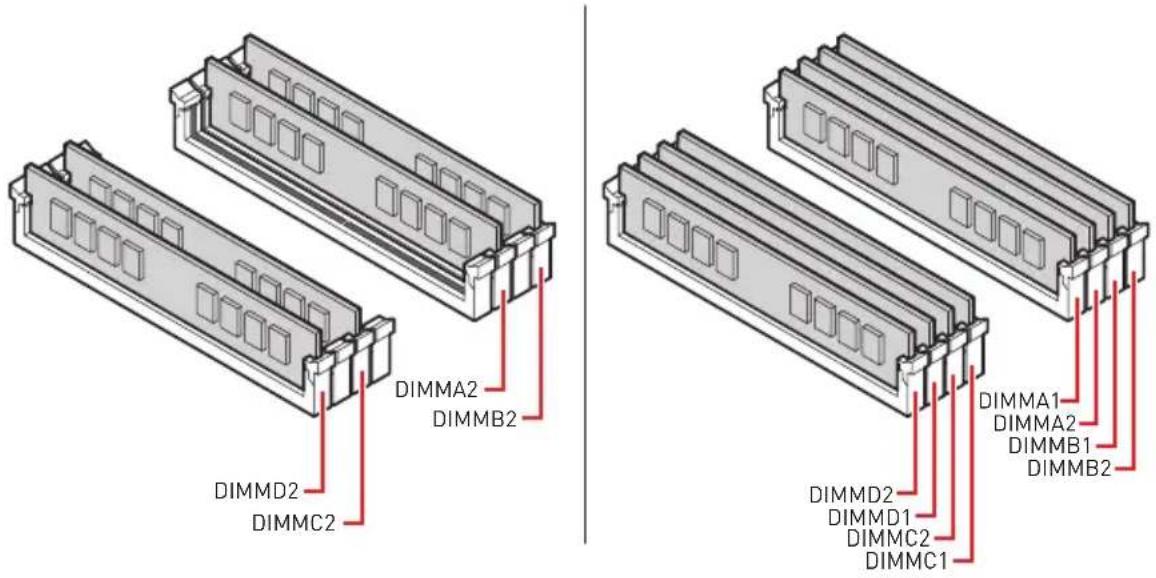
| D2 D1 C2 C1 CPU Socket A1 A2 B1 B2 | |||||||||
| 1 DIMM | 3rd Gen AMD RyzenTM ThreadripperTM Desktop Processors | √ | |||||||
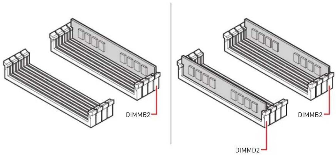
| 2 DIMMs | √ | √ | |||||||
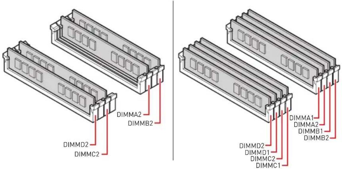
| 4 DIMMs | √ | √ | √ | √ | |||||
| 8 DIMMs | √ | √ | √ | √ | √ | √ | √ | √ | |
Important
Always insert memory modules in the DIMMB2 slot first.
To ensure system stability for Dual/ Triple/ Quad channel mode, memory modules must be of the same type, number and density.
Some memory modules may operate at a lower frequency than the marked value when overclocking due to the memory frequency operates dependent on its Serial Presence Detect (SPD). Go to BIOS and find the DRAM Frequency to set the memory frequency if you want to operate the memory at the marked or at a higher frequency.
It is recommended to use a more efficient memory cooling system for full DIMMs installation or overclocking.
The stability and compatibility of installed memory module depend on installed CPU and devices when overclocking.
Please refer www.msi.com for more information on compatible memory.
PCI_E1\~4: PCIe Expansion Slots
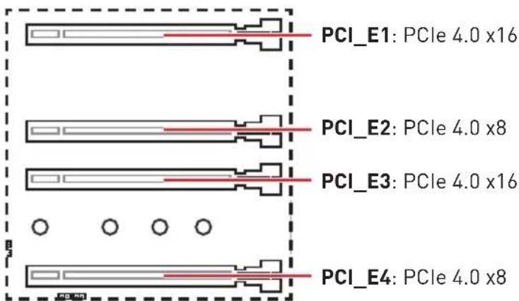
Multiple graphics cards installation recommendation
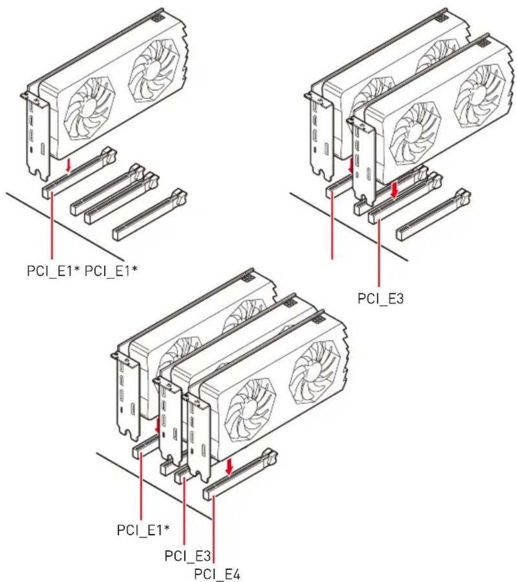
* To prevent monitor blank during the system POST. If you have multiple graphics cards installed, as marked above, connect your monitor to the graphics card located on the first PCIe x16 slot.
If you install a large and heavy graphics card, you need to use a tool such as MSI Gaming Series Graphics Card Bolster to support its weight to prevent deformation of the slot.
For a single PCIe x16 expansion card installation with optimum performance, using the PCI_E1 slot is recommended.
When adding or removing expansion cards, always turn off the power supply and unplug the power supply power cable from the power outlet. Read the expansion card's documentation to check for any necessary additional hardware or software changes.
Installing SLI graphics cards
For power supply recommendations for SLI configurations, please refer to the user guide of your graphics card to make sure you meet all the system requirements.
To install SLI graphics cards:
-
Turn off your computer and disconnect the power cord, install two graphics cards into the PCI_E1 and PCI_E3 slots.
-
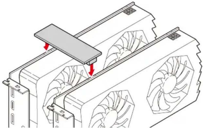
Connect the two cards together using the SLI Bridge Connector.
natural_image
Technical line drawing of a mechanical assembly with fan blades and a flat plate (no text or symbols)-
Connect all PCIe power connectors of the graphics cards.
-
Reconnect the power cord, power up the computer and install the drivers and software included in your graphics card package.
-
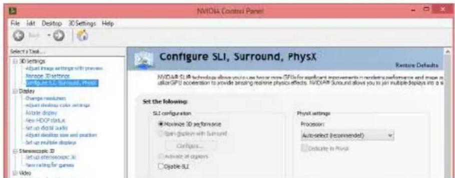
Right-click the Windows desktop and select NVIDIA Control Panel from the menu, click on Configure SLI, Surround, PhysX in the left task pane and select Maximize 3D performance in the SLI configuration menu, and then click Apply.
CPU\_PWR1\~2, ATX\_PWR1: Power Connectors
These connectors allow you to connect an ATX power supply.
natural_image
Diagram of a computer motherboard showing slots, connectors, and memory slots (no text or labels)| 1 5 4 8 CPU_PWR1/ CPU_PWR2 | |||
| 1 Ground 5 | +12V | ||
| 2 Ground 6 | +12V | ||
| 3 Ground 7 | +12V | ||
| 4 Ground 8 | +12V | ||
| 12 24 13 ATX_PWR1 | 1 +3.3V 13 +3.3V | ||
| 2 +3.3V 14 -12V | |||
| 3 Ground 15 Ground | |||
| 4 +5V 16 PS-ON# | |||
| 5 Ground 17 Ground | |||
| 6 +5V 18 Ground | |||
| 7 Ground 19 Ground | |||
| 8 PWR OK 20 Res | |||
| 9 5VSB 21 +5V | |||
| 10 +12V 22 +5V | |||
| 11 +12V 23 +5V | |||
| 12 +3.3V 24 Ground |

Important
- Make sure that all the power cables are securely connected to a proper ATX power supply to ensure stable operation of the motherboard.
- It is recommended to connect two 8-pin connectors or at least one 8-pin and one 4-pin power connectors to the CPU_PWR1 and CPU_PWR2 to optimize system stability and prevent the motherboard from overheating under heavy load.
- It is recommended to use a power supply with more than 750W.
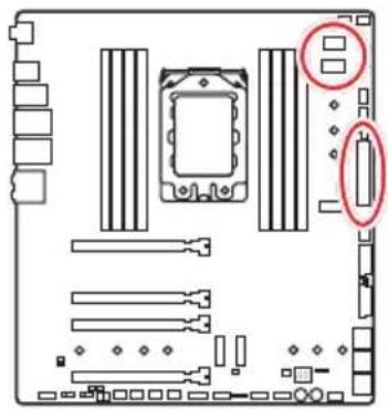
M2\_1\~3: M.2 Slots (Key M)
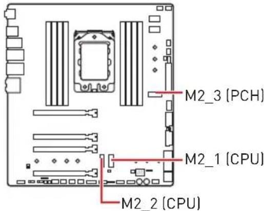

Watch the video to learn how to Install M.2 module.
http://youtu.be/JCTFABytrYA
Installing M.2 module
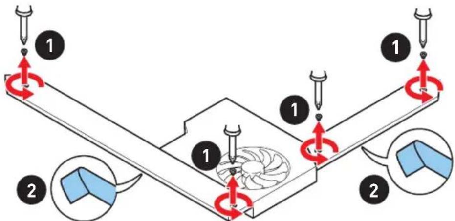
- Loosen the screws of M.2 SHIELD FROZR.
- Remove the M.2 SHIELD FROZR and remove the protective films from the thermal pads.
- Each M.2 slot is equipped with one standoff. To avoid damage to the M.2 SSD. If your M.2 SSD length is the same as the M.2 SHIELD FROZR heatsink, remove the standoff below the M.2 SSD slot.
- There are two thermal pads on each M.2 slot base plate. The thermal pad-2 is fixed on the M.2 Plate and should not be removed.
For double-side M.2 SSD, completely remove the thermal pad-1 and protection films.
For single-side M.2 SSD, remove the two thermal protection films from pad-1, then re-stick it to the thermal pad-2.
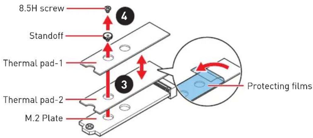

Pictures shown are for illustration purpose only and may differ from the actual plates and thermal pads.
- Move the position of the standoffs according to your M.2 SSDs length if need.
- Insert your M.2 SSD into the M.2 slot at a 30-degree angle.
- If the M.2 SSD is shorter than the M.2 SHIELD FROZR heatsink, place the 8.5H screw in the notch on the trailing edge of the M.2 module and tighten it into the standoff.
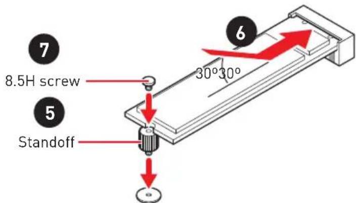
- Put the M.2 SHIELD FROZR heatsink back in place and secure it.
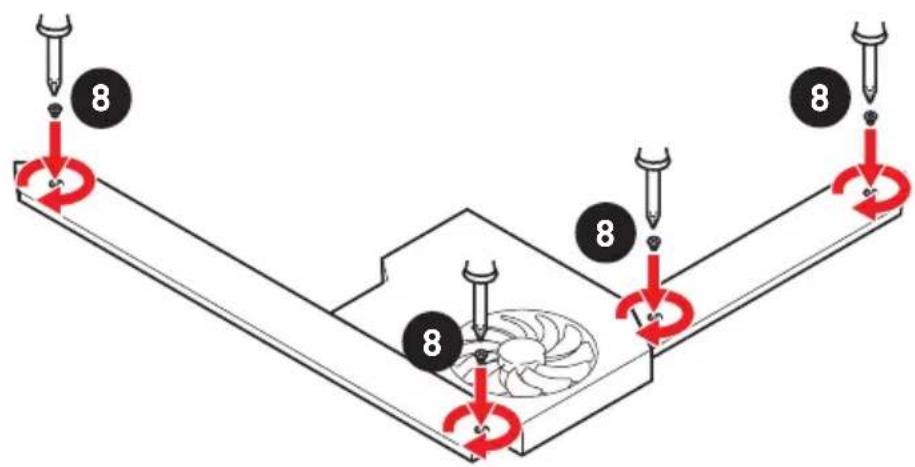
Installing M.2 XPANDER-AERO GEN4
To install the M.2 XPANDER-AERO GEN4 card, please follows the steps below.
- Remove the heatsink by loosening four screws on the back of the M.2 XPANDER-AERO GEN4 card.
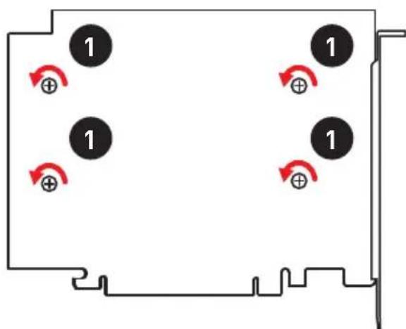
- Loosen M.2 screw from M.2 standoff.
- Loosen M.2 standoff.
- Move and fasten M.2 standoff to the appropriate location for your M.2 SSD.
- Insert your M.2 SSD into the M.2 slot at a 30-degree angle.
- Secure the M.2 device in place with M.2 screw.
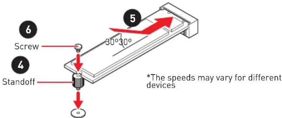
- Remove the protective film from the thermal pad of the heatsink.
- Reinstall and secure the heatsink with four heatsink screws.

natural_image
Diagram showing a blue curved shape inside a circle with a red arrow indicating direction, labeled with number 7 (no text or symbols beyond the number)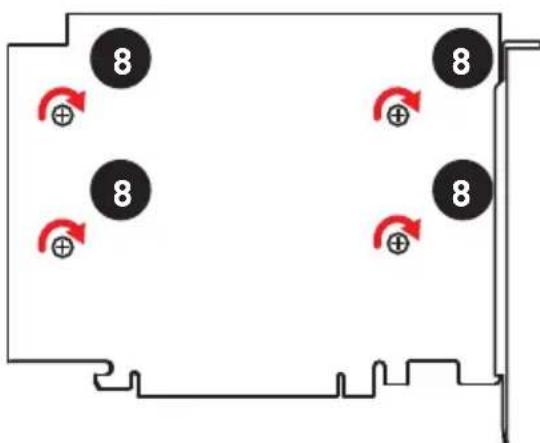
- Insert the M.2 XPANDER-AERO GEN4 card into the PCI_E3 slot.
- Use two screws to secure the M.2 XPANDER-AERO GEN4 card.
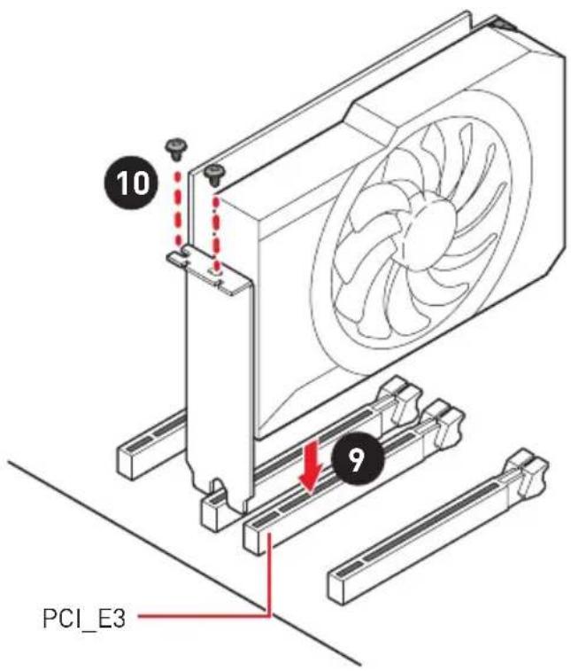
- Connect the PCIE_PWR1 to the power supply.
- Connect the case's HDD LED cable to the JCASE connector.
- Using the supplied HDD LED cable to connect the JMB connector and JFP1's HDD pins (pin 1 & pin3).
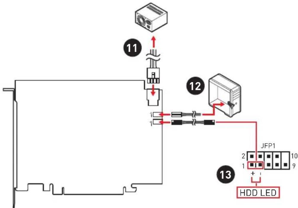
flowchart
graph TD
    A["Server"] -->|11| B["Switch"]
    B --> C["Device 12"]
    C --> D["Switch"]
    D --> E["HD LED"]
    E --> F["JFP1"]
    F --> G["2 1 9"]
    style A fill:#f9f,stroke:#333
    style B fill:#ccf,stroke:#333
    style C fill:#cfc,stroke:#333
    style D fill:#fcc,stroke:#333
    style E fill:#cff,stroke:#333
    style F fill:#ffc,stroke:#333
    style G fill:#cfc,stroke:#333
    note right of F: HDD LED
SATA1\~6: SATA 6Gb/s Connectors
These connectors are SATA 6Gb/s interface ports. Each connector can connect to one SATA device.
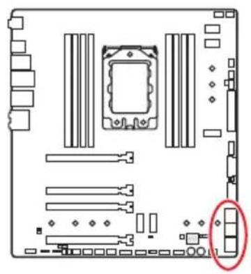
natural_image
Diagram of a computer motherboard showing CPU socket, RAM slots, and memory card (no text or labels)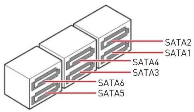

Please do not fold the SATA cable at a 90-degree angle. Data loss may result during transmission otherwise.
SATA cables have identical plugs on either sides of the cable. However, it is recommended that the flat connector be connected to the motherboard for space saving purposes.
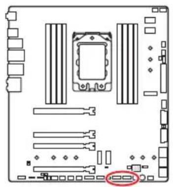
JFP1, JFP2: Front Panel Connectors
These connectors connect to the switches and LEDs on the front panel.
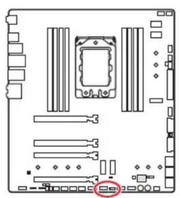
natural_image
Top-down view of a computer motherboard showing CPU socket and memory slots (no text or labels)| JFP1 | |||
| 1 HDD LED + 2 Power LED + | |||
| 3 HDD LED - 4 Power LED - | |||
| 5 Reset Switch 6 Power Switch | |||
| 7 Reset Switch 8 Power Switch | |||
| 9 Reserved 10 No Pin | |||
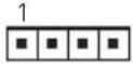 JFP2 JFP2 | 1 Speaker - 2 Buzzer + | ||
| 3 Buzzer - 4 | Speaker + | ||
JUSB1\~2: USB 2.0 Connectors
These connectors allow you to connect USB 2.0 ports on the front panel.
natural_image
Diagram of a computer motherboard showing slots, connectors, and a highlighted component (no text or labels)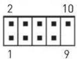 | |||
| 1 VCC 2 VCC | |||
| 3 USB0- 4 USB1- | |||
| 5 USB0+ 6 USB1+ | |||
| 7 Ground 8 Ground | |||
| 9 No Pin 10 NC | |||

Note that the VCC and Ground pins must be connected correctly to avoid possible damage.
In order to recharge your iPad, iPhone and iPod through USB ports, please install MSI CREATOR CENTER utility.
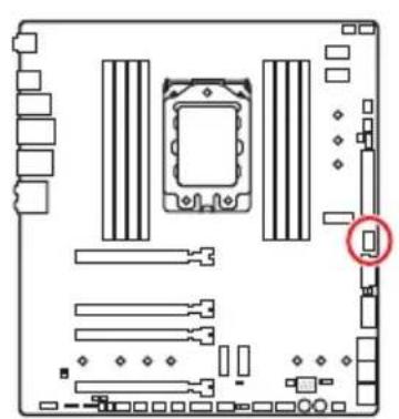
JUSB3: USB 3.2 Gen2 Type-C Connector
This connector allows you to connect the USB 3.2 Gen2 Type-C connector on the front panel. The connector possesses a foolproof design. When you connect the cable, be sure to connect it with the corresponding orientation.
natural_image
Top-down view of a computer motherboard showing CPU socket, RAM slots, and memory drive (no text or labels)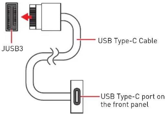
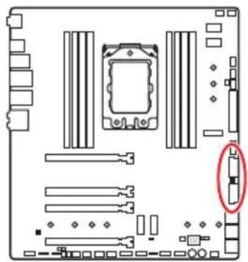
JUSB4\~5: USB 3.2 Gen1 Connectors
These connectors allow you to connect USB 3.2 Gen1 ports on the front panel.
natural_image
Diagram of a computer motherboard showing slots, connectors, and a highlighted component (no text or labels)| 10 11 20 | |||
| 1 Power 11 USB2.0+ | |||
| 2 USB3_RX_DN 12 USB2.0- | |||
| 3 USB3_RX_DP 13 Ground | |||
| 4 Ground 14 USB3_TX_C_DP | |||
| 5 | USB3_TX_C_DN | 15 | USB3_TX_C_DN |
| 6 | USB3_TX_C_DP | 16 Ground | |
| 7 Ground 17 USB3_RX_DP | |||
| 8 | USB2.0- | 18 | USB3_RX_DN |
| 9 | USB2.0+ | 19 | Power |
| 10 | NC | 20 | No Pin |

Note that the Power and Ground pins must be connected correctly to avoid possible damage.
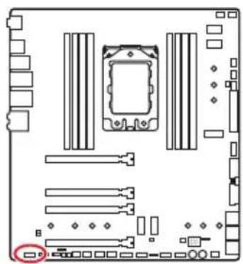
JAUD1: Front Audio Connector
This connector allows you to connect audio jacks on the front panel.
natural_image
Diagram of a computer motherboard showing CPU socket, RAM slots, and memory layout (no text or labels)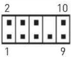 | |||
| 1 MIC L 2 Ground | |||
| 3 MIC R 4 NC | |||
| 5 Head Phone R | 6 | MIC Detection | |
| 7 SENSE_SEND 8 | No Pin | ||
| 9 Head Phone L 10 Head P | Phone | Detection | |
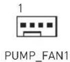
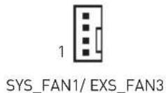
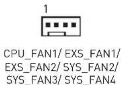
CPU\_FAN1, PUMP\_FAN1, SYS\_FAN1\~4, EXS\_FAN1\~3,: Fan Connectors
Fan connectors can be classified as PWM (Pulse Width Modulation) Mode or DC Mode. PWM Mode fan connectors provide constant 12V output and adjust fan speed with speed control signal. DC Mode fan connectors control fan speed by changing voltage. This motherboard can automatically detect PWM and DC mode. However, you can follow the instruction below to adjust the fan connector to PWM or DC Mode manually.
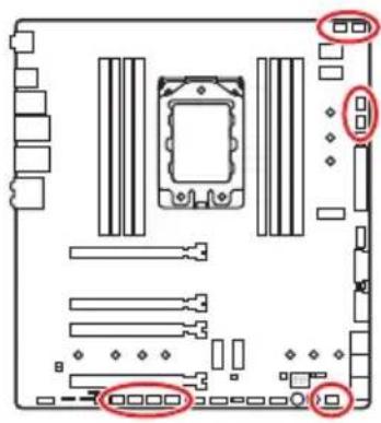
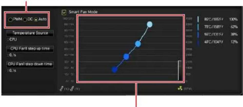
You can switch between PWM mode and DC mode and adjust fan speed in BIOS > HARDWARE MONITOR.
Select PWM mode or DC mode
line
| Smart Fan Mode | Temperature Source | |---|---| | 85°C/185F/ | CPU | | 79°C/158F/ | CPU Fan1 step up time | | 55°C/131F/ | 0.1s | | 49°C/104F/ | 0.1s |There are gradient points of the fan speed that allow you to adjust fan speed in relation to CPU temperature.
Pin definition of fan connectors
| PWM Mode pin definition | |||
| 1 Ground 2 +12V | |||
| 3 Sense 4 Speed Control Signal | |||
| DC Mode pin definition | |||
| 1 G | round 2 Voltage | Control | |
| 3 S | Sense 4 NC | ||
T\_SEN1\~3: Thermal Sensor Connectors
These connectors allow you to connect the thermistor cable and use it to monitor the temperature of the detection point.
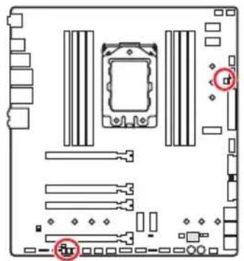
natural_image
Diagram of a computer motherboard showing CPU socket, RAM slots, and drive bays (no text or labels)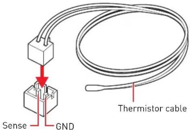
JBLK\_D1, JBLK\_U1: Base Clock Down & Up Header
These connectors allow you to connect the buttons separately and then press the button to turn the CPU base clock down or up.
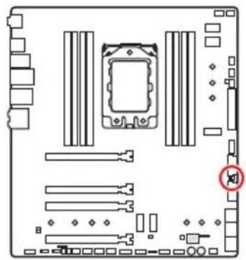
natural_image
Diagram of a computer motherboard showing slots, connectors, and a highlighted component (no text or labels)JBLK_D1 (Decrease CPU base clock)
JBLK_U1 (Increase CPU base clock)
POWER1, RESET1: Power Button, Reset Button
The Power / Reset button allows you to power on / reset the computer.
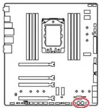
natural_image
Diagram of a computer motherboard layout showing slots, connectors, and a highlighted circular component (no text or labels)
Reset button
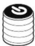
Power button
JTPM1: TPM Module Connector
This connector is for TPM (Trusted Platform Module). Please refer to the TPM security platform manual for more details and usages.
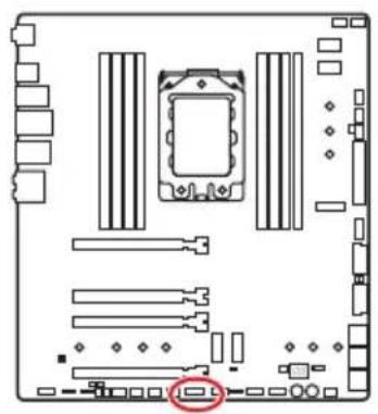
natural_image
Diagram of a computer motherboard showing CPU socket, RAM slots, and memory drive (no text or labels)2 14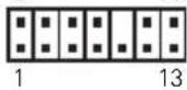 | |||
| 1 LPC Clock 2 3V Standby power | |||
| 3 LPC Reset 4 3.3V Power | |||
| 5 LPC address & data pin0 6 Serial IRQ | |||
| 7 LPC address & data pin1 8 5V Power | |||
| 9 LPC address & data pin2 10 No Pin | |||
| 11 LPC address & data pin3 12 Ground | |||
| 13 | LPC Frame | 14 Ground | |
JBAT1: Clear CMOS (Reset BIOS) Jumper
There is CMOS memory onboard that is external powered from a battery located on the motherboard to save system configuration data. If you want to clear the system configuration, set the jumper to clear the CMOS memory.
natural_image
Diagram of a computer motherboard showing slots, CPU socket, and connectors (no text or labels)
Keep Data (default)

Clear CMOS/ Reset BIOS
Resetting BIOS to default values
- Power off the computer and unplug the power cord
- Use a jumper cap to short JBAT1 for about 5-10 seconds.
- Remove the jumper cap from JBAT1.
- Plug the power cord and power on the computer.
JCI1: Chassis Intrusion Connector
This connector allows you to connect the chassis intrusion switch cable.
natural_image
Diagram of a computer motherboard showing CPU socket, RAM slots, and drive bays (no text or labels)
Normal (default)

Trigger the chassis intrusion event
Using chassis intrusion detector
- Connect the JCI1 connector to the chassis intrusion switch/ sensor on the chassis.
- Close the chassis cover.
- Go to BIOS > SETTINGS > Security > Chassis Intrusion Configuration.
- Set Chassis Intrusion to Enabled.
- Press F10 to save and exit and then press the Enter key to select Yes.
- Once the chassis cover is opened again, a warning message will be displayed on screen when the computer is turned on.
Resetting the chassis intrusion warning
- Go to BIOS > SETTINGS > Security > Chassis Intrusion Configuration.
- Set Chassis Intrusion to Reset.
- Press F10 to save and exit and then press the Enter key to select Yes.
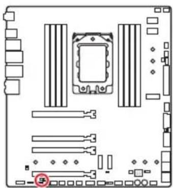
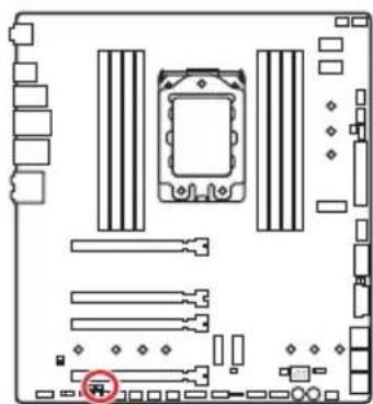
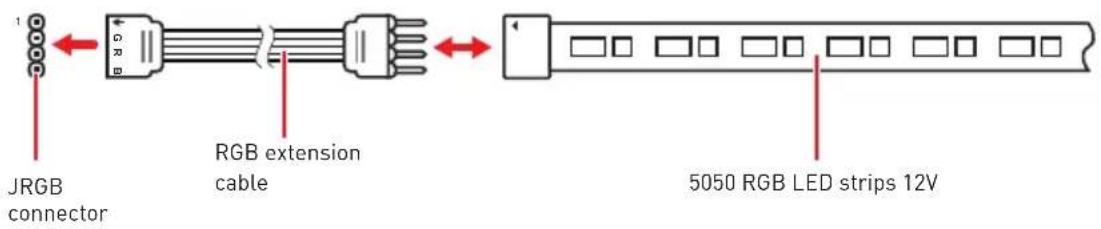
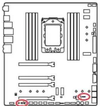
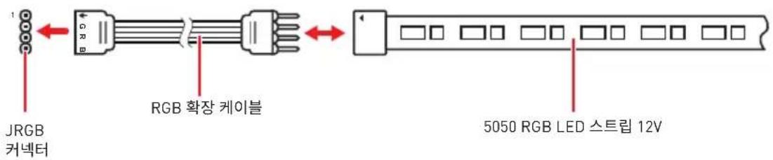
JRGB1: RGB LED connector
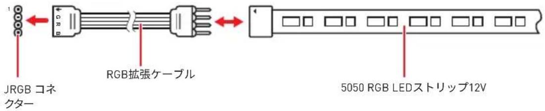
The JRGB connector allows you to connect the 5050 RGB LED strips 12V.
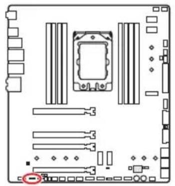
natural_image
Diagram of a computer motherboard showing CPU socket, RAM slots, and memory drive (no text or labels)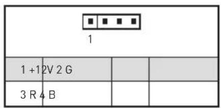
RGB LED Strip Connection
RGB LED Fan Connection
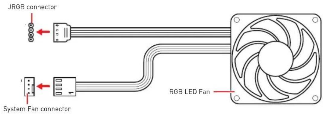

The JRGB connector supports up to 2 meters continuous 5050 RGB LED strips (12V/G/R/B) with the maximum power rating of 3A (12V).
Always turn off the power supply and unplug the power cord from the power outlet before installing or removing the RGB LED strip.
Please use MSI's software to control the extended LED strip.
JRAINBOW1\~2: Addressable RGB LED connectors
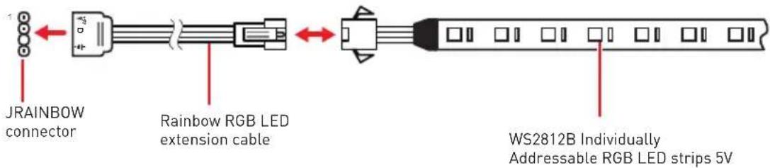
The JRAINBOW connectors allow you to connect the WS2812B Individually Addressable RGB LED strips 5V.
natural_image
Diagram of a computer motherboard showing slots, connectors, and a central CPU socket (no text or labels)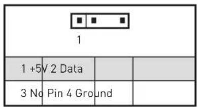
Addressable RGB LED Strip Connection
Addressable RGB LED Fan Connection
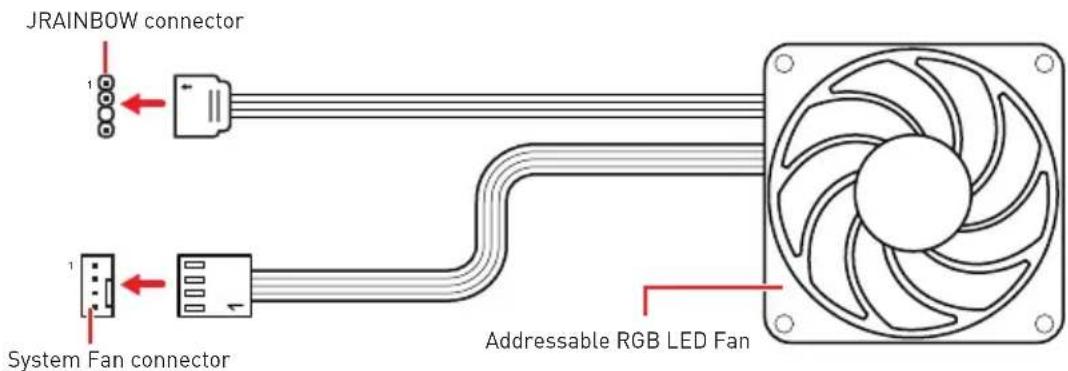

Do not connect the wrong type of LED strips. The JRGB connector and the JRAINBOW connector provide different voltages, and connecting the 5V LED strip to the JRGB connector will result in damage to the LED strip.

The JRAINBOW connector supports up to 75 LEDs WS2812B Individually Addressable RGB LED strips (5V/Data/Ground) with the maximum power rating of 3A (5V). In the case of 20% brightness, the connector supports up to 200 LEDs.
Always turn off the power supply and unplug the power cord from the power outlet before installing or removing the RGB LED strip.
Please use MSI's software to control the extended LED strip.
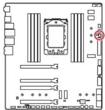
JCORSAIR1: CORSAIR Connector
The JCORSAIR1 connector allows you to connect the CORSAIR Individually Addressable RGB LED strips 5V or CORSAIR RGB LED fans with the CORSAIR fan hub. Once all items are connected properly, you can control the CORSAIR RGB LED strips and fans with MSI's software.
natural_image
Diagram of a computer motherboard layout showing slots, connectors, and a highlighted component (no text or labels)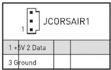
CORSAIR RGB LED Fan Connection
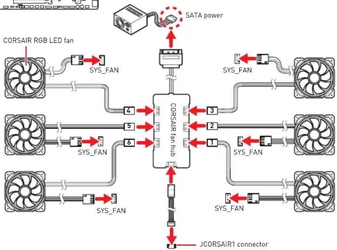
flowchart
graph TD
    A["SATA power"] --> B["CorSAIR fan hub"]
    C["CORSAIR RGB LED fan"] --> D["SYS_FAN"]
    D --> E["4"]
    D --> F["5"]
    D --> G["6"]
    H["JSYS_FAN"] --> I["1"]
    I --> J["2"]
    I --> K["3"]
    L["JSYS_FAN"] --> M["1"]
    M --> N["2"]
    M --> O["3"]
    P["JSYS_FAN"] --> Q["1"]
    Q --> R["2"]
    Q --> S["3"]
    T["JCORSAIR1 connector"] --> U["1"]
    U --> V["2"]
    V --> W["3"]
    X["SATA power"] --> Y["CorSAIR fan hub"]
    style A fill:#f9f,stroke:#333
    style C fill:#f9f,stroke:#333
    style L fill:#f9f,stroke:#333
    style P fill:#f9f,stroke:#333
    style T fill:#f9f,stroke:#333
CORSAIR Lighting Node PRO Connection

Fans must start at 1 and continue in series. 1 > 2 > 3 > 4 > 5 > 6 . Any fan not connected in series will break communication and the RGB LED lighting function will not work.
Quantity of RGB LED Fans or RGB LED Lighting PRO strips supported may differ between models. Please refer to the motherboard specification.
CORSAIR RGB LED Fan and CORSAIR Lighting Node PRO can't be used at the same time.
J0C\_RT1: OC Retry Button
This connector allows you to connect a button. When you press and hold the button, the system will keep retrying OC items until it boot up successfully.
JOC\_FS1: OC Force Enter BIOS Button
This connector allows you to connect a button. When you press the button, the system will be forced into BIOS without showing the OC_FAIL message.
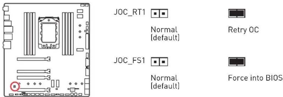
JOC_RT1
Normal (default)
Retry OC
JOC_FS1
Normal (default)
Force into BIOS
JSLOW1: Slow Mode Booting Jumper
This jumper is used for LN2 cooling solution, that provides the extreme overclocking conditions, to boot at a stable processor frequency and to prevent the system from crashing.
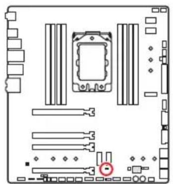
natural_image
Diagram of a computer motherboard showing slots, connectors, and a central CPU socket (no text or labels)
Normal (default)

Enable (Please enable this jumper during BIOS POST.)

Users will try extreme low temperature (must be higher than -124 degrees to prevent Debug Code 00) overclocking at their own risks.
The overclocking results will vary according to the CPU version.
Please don't set to Enabled when the system is powered off or can't be started.
Onboard LEDs
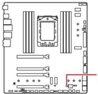
EZ Debug LED
These LEDs indicate the debug status of the motherboard.
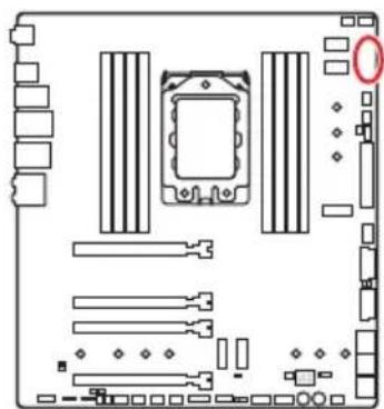
natural_image
Diagram of a computer motherboard layout showing slots, connectors, and a highlighted component (no text or labels)□ CPU - indicates CPU is not detected or fail.
☐ DRAM - indicates DRAM is not detected or fail.
VGA - indicates GPU is not detected or fail.
☐ BOOT - indicates the booting device is not detected or fail.
JPWRLED1: LED power input
This connector is used by retailers to demonstrate onboard LED light effects.
natural_image
Diagram of a computer motherboard layout showing CPU socket, RAM slots, and drive bays (no text or labels)JPWRLED1 - LED power input
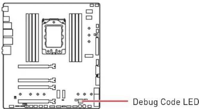
Debug Code LED
The Debug Code LED displays progress and error codes during and after POST. Refer to the Debug Code LED table for details.
Hexadecimal Character Table
| Hexadecimal 0 | 1 2 | 3 4 5 | 6 7 | 8 9 A | B C | D E | F | ||||||||
| Debug CodeLED display | 0 | 12 | 34 | 56 | 78 | 9A | B | C | dEF |
Boot Phases
Security (SEC) - initial low-level initialization
Pre-EFI Initialization (PEI) - memory initialization
Driver Execution Environment (DXE) - main hardware initialization
Boot Device Selection (BDS) – system setup, pre-OS user interface & selecting a bootable device (CD/DVD, HDD, USB, Network, Shell, ...)
Debug Code LED Table
SEC Progress Codes
| 01 Power on. Reset type detection (soft/hard) |
| 02 AP initialization before microcode loading |
| 03 System Agent initialization before microcode loading |
| 04 PCH initialization before microcode loading |
| 06 Microcode loading |
| 07 AP initialization after microcode loading |
| 08 System Agent initialization after microcode loading |
| 09 PCH initialization after microcode loading |
| 0B Cache initialization |
SEC Error Codes
| OC - OD Reserved for future AMI SEC error codes |
| OE Microcode not found |
| OF Microcode not loaded |
PEI Progress Codes
| 10 PEI Core is started | |
| 11 Pre-memory CPU initialization is started | |
| 12 - 14 Pre-memory CPU initialization (CPU module specific) | |
| 15 Pre-memory System Agent initialization is started | |
| 16 - 18 Pre-Memory System Agent initialization (System Agent module specific) | |
| 19 Pre-memory PCH initialization is started | |
| 1A - 1C Pre-memory PCH initialization (PCH module specific) | |
| 2B Memory initialization. Serial Presence Detect (SPD) data reading | |
| 2C Memory initialization. Memory presence detection | |
| 2D Memory initialization. Programming memory timing information | |
| 2E Memory initialization. Configuring memory | |
| 2F Memory initialization (other) | |
| 31 Memory Installed | |
| 32 CPU post-memory initialization is started | |
| 33 CPU post-memory initialization. Cache initialization | |
| 34 | CPU post-memory initialization. Application Processor(s) (AP) initialization |
| 35 CPU post-memory initialization. Boot Strap Processor (BSP) selection | |
| 36 | CPU post-memory initialization. System Management Mode (SMM) initialization |
| 37 Post-Memory System Agent initialization is started | |
| 38 - 3A Post-Memory System Agent initialization (System Agent module specific) | |
| 3B Post-Memory PCH initialization is started | |
| 3C - 3E Post-Memory PCH initialization (PCH module specific) | |
| 4F DXE IPL is started | |
PEI Error Codes
| 4B Memory not installed (For Summit CPU) |
| E0 Memory not installed (For Bristol CPU) |
DXE Progress Codes
| 60 DXE Core is started | |
| 61 NVRAM initialization | |
| 62 Installation of the PCH Runtime Services | |
| 63 CPU DXE initialization is started | |
| 64 - 67 CPU DXE initialization (CPU module specific) | |
| 68 PCI host bridge initialization | |
| 69 System | Agent DXE initialization is started |
| 6A System | Agent DXE SMM initialization is started |
| 6B - 6F System Agent DXE initialization (System Agent module specific) | |
| 70 PCH DXE initialization is started | |
| 71 PCH DXE SMM initialization is started | |
| 72 PCH devices initialization | |
| 73 - 77 PCH DXE Initialization (PCH module specific) | |
| 78 ACPI module initialization | |
| 79 CSM initialization | |
| 7A - 7F Reserved for future AMI DXE codes | |
| 90 Boot Device Selection (BDS) phase is started | |
| 91 Driver connecting is started | |
| 92 PCI Bus initialization is started | |
| 93 PCI Bus Hot Plug Controller Initialization | |
| 94 PCI Bus Enumeration 32 | |
| 95 PCI Bus Request Resources | |
| 96 PCI Bus Assign Resources | |
| 97 Console Output devices connect | |
| 98 Console input devices connect | |
| 99 Super IO Initialization | |
| 9A USB initialization is started | |
| 9B USB Reset | |
| 9C USB Detect | |
| 9D USB Enable | |
| 9E -9F Reserved for future AMI codes | |
| A0 IDE initialization is started | |
| A1 IDE Reset | |
| A2 IDE Detect | |
| A3 IDE Enable | |
| A4 SCSI initialization is started | |
| A5 SCSI Reset | |
| A6 SCSI Detect | |
| A7 SCSI Enable | |
| A8 Setup Verifying Password | |
| A9 Start of Setup | |
| AB Setup Input Wait | |
| AD Ready | To Boot event |
| AE Legacy | Boot event |
| AF Exit Boot Services event | |
| B0 Runtime | Set Virtual Address MAP Begin |
| B1 Runtime | Set Virtual Address MAP End |
| B2 Legacy | Option ROM Initialization |
| B3 System | Reset |
| B4 USB hot plug | |
| B5 PCI bus | hot plug |
| B6 Clean-up of NVRAM | |
| B7 Configuration Reset (reset of NVRAM settings) | |
| B8 - BF Reserved for future AMI codes | |
DXE Error Codes
| D0 CPU in | tialization error |
| D1 System | Agent initialization error |
| D2 PCH in | tialization error |
| D3 Some of the Architectural Protocols are not available | |
| D4 PCI resource allocation error. Out of Resources | |
| D5 No Space for Legacy Option ROM | |
| D6 No Console Output Devices are found | |
| D7 No Console Input Devices are found | |
| D8 Invalid | password |
| D9 Error loading Boot Option (LoadImage returned error) | |
| DA Boot Option is failed (StartImage returned error) | |
| DB Flash update is failed | |
| DC Reset protocol is not available | |
S3 Resume Progress Codes
| E0 S3 Resume is stared (S3 Resume PPI is called by the DXE IPL) | |
| E1 S3 Boot Script execution | |
| E2 Video repost | |
| E3 OS S3 wake vector call | |
| E4 - E7 Reserved for future AMI progress codes |
S3 Resume Error Codes
| E8 S3 Resume Failed |
| E9 S3 Resume PPI not Found |
| EA S3 Resume Boot Script Error |
| EB S3 OS | Wake Error |
| EC - EF | Reserved for future AMI error codes |
Recovery Progress Codes
| F0 Recovery condition triggered by firmware (Auto recovery) | |
| F1 Recovery condition triggered by user (Forced recovery) | |
| F2 Recovery process started | |
| F3 Recovery firmware image is found | |
| F4 Recovery firmware image is loaded | |
| F5 - F7 Reserved for future AMI progress codes |
Recovery Error Codes
| F8 Recovery PPI is not available | |
| F9 Recovery capsule is not found | |
| FA Invalid recovery capsule | |
| FB - FF Reserved for future AMI error codes |
ACPI States Codes
The following codes appear after booting and the operating system into ACPI modes.
| 01 System | is entering S1 sleep state |
| 02 System | is entering S2 sleep state |
| 03 System | is entering S3 sleep state |
| 04 System | is entering S4 sleep state |
| 05 System | is entering S5 sleep state |
| 10 System | is waking up from the S1 sleep state |
| 20 System | is waking up from the S2 sleep state |
| 30 System | is waking up from the S3 sleep state |
| 40 System | is waking up from the S4 sleep state |
| AC | System has transitioned into ACPI mode. Interrupt controller is in PIC mode. |
| AA | System has transitioned into ACPI mode. Interrupt controller is in APIC mode. |
Installing OS, Drivers & Utilities
Please download and update the latest utilities and drivers at www.msi.com
Installing Windows ^® 10
- Power on the computer.
- Insert the Windows ^® 10 installation disc/USB into your computer.
- Press the Restart button on the computer case.
- Press F11 key during the computer POST (Power-On Self Test) to get into Boot Menu.
- Select the Windows ^® 10 installation disc/USB from the Boot Menu.
- Press any key when screen shows Press any key to boot from CD or DVD... message.
- Follow the instructions on the screen to install Windows ^® 10.
Installing Drivers
- Start up your computer in Windows ^® 10.
- Insert MSI ^® USB Drive into the USB port.
- Click the Select to choose what happens with removable drives pop-up notification, then select Run DVDSetup.exe to open the installer. If you turn off the AutoPlay feature from the Windows Control Panel, you can still manually execute the DVDSetup.exe from the root path of the MSI USB Drive.
- The installer will find and list all necessary drivers in the Drivers/Software tab.
- Click the Install button in the lower-right corner of the window.
- The drivers installation will then be in progress, after it has finished it will prompt you to restart.
- Click OK button to finish.
- Restart your computer.
Installing Utilities
Before you install utilities, you must complete drivers installation.
- Open the installer as described above.
- Click the Utilities tab.
- Select the utilities you want to install.
- Click the Install button in the lower-right corner of the window.
- The utilities installation will then be in progress, after it has finished it will prompt you to restart.
- Click OK button to finish.
- Restart your computer.
BIOS Setup
The default settings offer the optimal performance for system stability in normal conditions. You should always keep the default settings to avoid possible system damage or failure booting unless you are familiar with BIOS.

BIOS items are continuously update for better system performance. Therefore, the description may be slightly different from the latest BIOS and should be for reference only. You could also refer to the HELP information panel for BIOS item description.
The pictures in this chapter are for reference only and may vary from the product you purchased.
Entering BIOS Setup
Press Delete key, when the Press DEL key to enter Setup Menu, F11 to enter Boot Menu message appears on the screen during the boot process.
Function key
F1: General Help
F2: Add/ Remove a favorite item
F3: Enter Favorites menu
F4: Enter CPU Specifications menu
F5: Enter Memory-Z menu
F6: Load optimized defaults
F7: Switch between Advanced mode and EZ mode
F8: Load Overclocking Profile
F9: Save Overclocking Profile
F10: Save Change and Reset*
F12: Take a screenshot and save it to USB flash drive (FAT/ FAT32 format only).
Ctrl+F: Enter Search page
* When you press F10, a confirmation window appears and it provides the modification information. Select between Yes or No to confirm your choice.
Resetting BIOS
You might need to restore the default BIOS setting to solve certain problems. There are several ways to reset BIOS:
- Go to BIOS and press F6 to load optimized defaults.
- Short the Clear CMOS jumper on the motherboard.

Be sure the computer is off before clearing CMOS data. Please refer to the Clear CMOS jumper section for resetting BIOS.
Updating BIOS
Updating BIOS with M-FLASH
Before updating:
Please download the latest BIOS file that matches your motherboard model from MSI website. And then save the BIOS file into the USB flash drive.
Updating BIOS:
- Insert the USB flash drive that contains the update file into the USB port.
-
Please refer the following methods to enter flash mode.
-
Reboot and press Ctrl + F5 key during POST and click on Yes to reboot the system.
-
Reboot and press Del key during POST to enter BIOS. Click the M-FLASH button and click on Yes to reboot the system.
-
Select a BIOS file to perform the BIOS update process.
- After the flashing process is 100% completed, the system will reboot automatically.
Updating the BIOS with MSI CREATOR CENTER
Before updating:
Make sure the LAN driver is already installed and the Internet connection is set properly.
Updating BIOS:
- Install and launch MSI CREATOR CENTER.
- Select BIOS Update.
- Click on Scan button.
- Click on Download icon to download and install the latest BIOS file.
- Click Next and choose In Windows mode. And then click Next and Start to start updating BIOS.
- After the flashing process is 100% completed, the system will restart automatically.
Updating BIOS with Flash BIOS Button
- Please download the latest BIOS file that matches your motherboard model from the MSI® website.
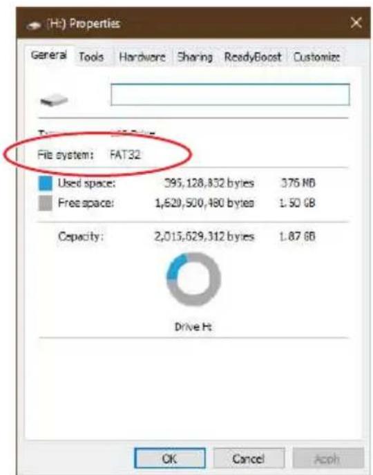
- Rename the BIOS file to MSI.ROM, and save it to the root of your USB flash drive (FAT32 format).
- Connect the power supply to CPU_PWR1 and ATX_PWR1. (No need to install CPU and memory.)
- Plug the USB flash drive that contains the MSI.ROM file into the Flash BIOS Port on the rear I/O panel.
- Press the Flash BIOS Button to flash BIOS, and the LED starts flashing.
- The LED will be turned off when the process is completed.

Only the FAT32 format USB flash drive supports updating BIOS by Flash BIOS Button. To check your drive, go to Windows Explorer, right click on the drive icon and go to Properties.
EZ Mode
At EZ mode, it provides the basic system information and allows you to configure the basic setting. To configure the advanced BIOS settings, please enter the Advanced Mode by pressing the Setup Mode switch or F7 function key.
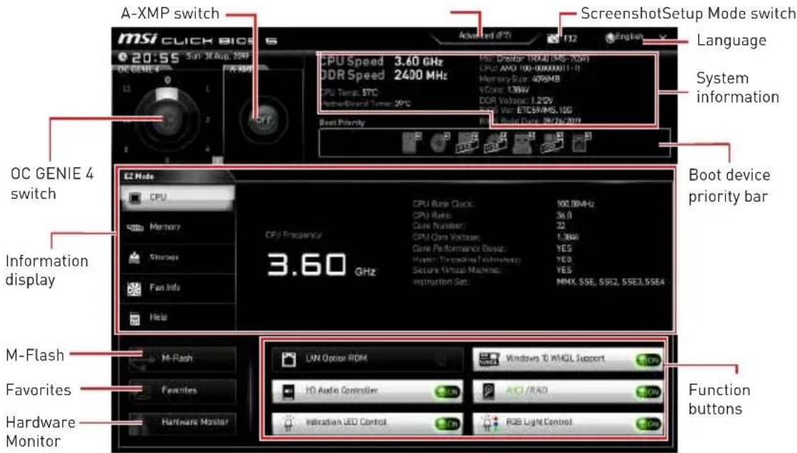
- OC GENIE 4 switch - click to select the overclocking stage as you desire. Read the abilities of OC GENIE 4 by clicking on the question mark in the right-bottom corner. This function will only be available if the installed processor supports this function. To disable OC GENIE 4, select 0.

Please don't make any changes in OC menu and don't load defaults to keep the optimal performance and system stability after activating the OC GENIE 4 function.
- A-XMP switch (optional) - click on the inner circle to enable/ disable the A-XMP. Switch the outer circle to select the memory profile if any. This switch will only be available if the installed processor and memory modules support this function.
- Setup Mode switch - press this tab or the F7 key to switch between Advanced mode and EZ mode.
- Screenshot - click on this tab or the F12 key to take a screenshot and save it to USB flash drive (FAT/ FAT32 format only).
- Search - click on this tab or the Ctrl+F keys and the search page will show. It allows you to search by BIOS item name, enter the item name to find the item listing. Move the mouse over a blank space and right click the mouse to exit search page.

In search page, only the F6, F10 and F12 function keys are available.
- Language - allows you to select the language of BIOS setup.
- System information - shows the CPU/ DDR speed, CPU/ MB temperature, MB/ CPU type, memory size, CPU/ DDR voltage, BIOS version and build date.
- Boot device priority bar - you can move the device icons to change the boot priority. The boot priority from high to low is left to right.
- Information display - click on the CPU, Memory, Storage, Fan Info and Help buttons on left side to display related information.
- Function buttons - enable or disable the functions by clicking on their respective button.
- M-Flash - click on this button to display the M-Flash menu that provides the way to update BIOS with a USB flash drive.
- Hardware Monitor - click on this button to display the Hardware Monitor menu that allows you to manually control the fan speed by percentage.
- Favorites - press the Favorites tab or the F3 key to enter Favorites menu. It allows you to create personal BIOS menu where you can save and access favorite/frequently-used BIOS setting items.
- Default HomePage - allows you to select a BIOS menu (e.g. SETTINGS, OC...,etc) as the BIOS home page.
- Favorite1\~5 - allows you to add the frequently-used/ favorite BIOS setting items in one page.
-
To add a BIOS item to a favorite page (Favorite 1\~5)
-
Move the mouse over a BIOS item not only on BIOS menu but also on search page.
- Right-click or press F2 key.
- Choose a favorite page and click on OK.
- To delete a BIOS item from favorite page
- Move the mouse over a BIOS item on favorite page (Favorite 1\~5)
- Right-click or press F2 key.
- Choose Delete and click on OK.
Advanced Mode
Press Setup Mode switch or F7 function key can switch between EZ Mode and Advanced Mode in BIOS setup.
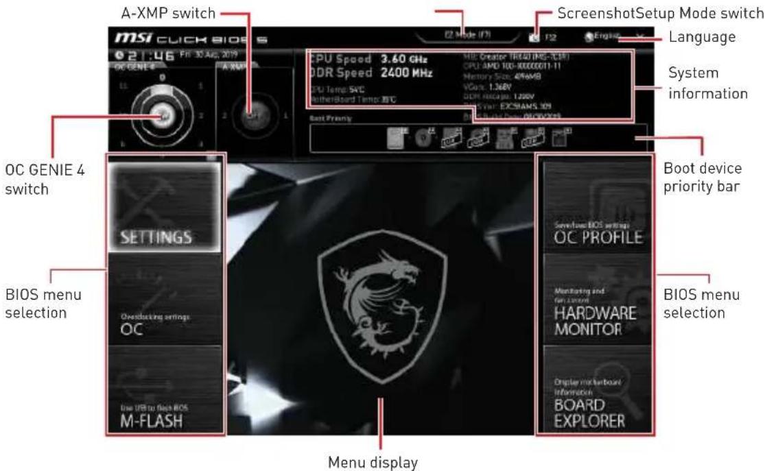
- BIOS menu selection - the following options are available:
- SETTINGS - allows you to specify the parameters for chipset and boot devices.
- OC - allows you to adjust the frequency and voltage. Increasing the frequency may get better performance.
- M-FLASH - provides the way to update BIOS with a USB flash drive.
- OC PROFILE - allows you to manage overclocking profiles.
- HARDWARE MONITOR - allows you to set the speeds of fans and monitor voltages of system.
- BOARD EXPLORER - provides the information of installed devices on this motherboard.
- Menu display - provides BIOS setting items and information to be configured.
OC Menu
This menu is for advanced users who want to overclock the motherboard.
![OC Experience Mode [Normal] CPU Setting CPU Rate Auto Adjusted CPU Frequency 300MHz Advanced CPU Configuration Game Base Function Control [By BICS Options] CPU, BCLK Setting CPU Base Clock (MHz) Auto Direct CC Button [Enabled] Clockgen Features DRAM Setting A-IMP [Disabled] Profile: CERA 240MHz 1st-to-1st DRAM Frequency [Auto] Adjusted DRAM Frequency 240MHz FCLK Frequency [Auto] UCLK DIV MODE [Auto] Memory Failure Retry [Enabled] Advanced DRAM Configuration](/content/2026/05/877918/images/58516b0640aa412146a812d828d1ea39e587e88ad940f6b3e8f87300cd079576.jpg)

Overclocking your PC manually is only recommended for advanced users.
Overclocking is not guaranteed, and if done improperly, it could void your warranty or severely damage your hardware.
If you are unfamiliar with overclocking, we advise you to use OC GENIE 4 function for easy overclocking.
The BIOS items in OC menu will vary with the processor.
▶ OC Explore Mode [Normal]
Enables or disables to show the normal or expert version of OC settings.
[Normal] Provides the regular OC settings in BIOS setup.
[Expert] Provides the advanced OC settings for OC expert to configure in BIOS setup.
Note: We use * as the symbol for the OC settings of Expert mode.
▶ CPU Ratio [Auto]
Sets the CPU ratio that is used to determine CPU clock speed. This item can only be changed if the processor supports this function.
▶ Advanced CPU Configuration
Press Enter to enter the sub-menu. User can set the parameters about CPU power/ current. The system may become unstable or unbootable after changing the parameters. If it occurs, please clear the CMOS data and restore the default settings.
▶ A-XMP [Disabled]
Please enable A-XMP or select a profile of memory module for overclocking the memory. This item will be available when the installed memory modules, processor and motherboard support this function.
▶ DRAM Frequency [Auto]
Sets the DRAM frequency. Please note the overclocking behavior is not guaranteed.
▶ Memory Try It ! [Disabled]
It can improve memory compatibility or performance by choosing optimized memory preset.
▶ Memory Failure Retry
[Enabled] Allows system attempt reboot. If failed in the end, system will boot up with default settings safely.
[Disabled] System would not boot up due OC fail, it requires clear CMOS to restore system default settings.
▶ Advanced DRAM Configuration (optional)
Press Enter to enter the sub-menu. User can set the memory timing for each/ all memory channel. The system may become unstable or unbootable after changing memory timing. If it occurs, please clear the CMOS data and restore the default settings. (Refer to the Clear CMOS jumper/ button (optional) section to clear the CMOS data, and enter the BIOS to load the default settings.)
▶ DigitALL Power
Press Enter to enter the sub-menu. Controls the digital powers related to CPU PWM.
▶ CPU Voltages control [Auto]
These options allows you to set the voltages related to CPU. If set to Auto, BIOS will set these voltages automatically or you can set it manually.
▶ DRAM Voltages control [Auto]
These options allows you to set the voltages related to memory. If set to Auto, BIOS will set these voltages automatically or you can set it manually.
▶ Memory Changed Detect [Enabled]\*
Enables or disables the system to issue a warning message during boot when the memory has been replaced.
[Enabled] The system will issue a warning message during boot and then you have to load the default settings for new devices.
[Disabled] Disables this function and keeps the current BIOS settings.
▶ CPU Specifications
Press Enter to enter the sub-menu. This sub-menu displays the information of installed CPU. You can also access this information menu at any time by pressing [F4]. Read only.
▶ CPU Technology Support
Press Enter to enter the sub-menu. The sub-menu shows the key features of installed CPU. Read only.
▶ MEMORY-Z
Press Enter to enter the sub-menu. This sub-menu displays all the settings and timings of installed memory. You can also access this information menu at any time by pressing [F5].
DIMMx Memory SPD
Press Enter to enter the sub-menu. The sub-menu displays the information of installed memory. Read only.
▶ CPU Features
Press Enter to enter the sub-menu.
▶ Simultaneous Multi-Threading [Enabled] (optional)
Enables/disables the AMD Simultaneous Multi-Threading. This item appears when the installed CPU supports this technology.
▶ Global C-state Control [Enabled] (optional)
Enables/disables IO based C-state generation and DF C-states.
▶ Opcache Control [Auto] (optional)
Enables/ disables Opcache. Opcache stores recently decode instruction to save the decoding time when the instruction is repeated. And ist may increase the CPU performance and reduce the power consumption slightly.
▶ IOMMU Mode (optional)
Enables/disables the IOMMU (I/O Memory Management Unit) for I/O Virtualization.
▶ Spread Spectrum (optional)
This function reduces the EMI (Electromagnetic Interference) generated by modulating clock generator pulses.
[Enabled] Enables the spread spectrum function to reduce the EMI (Electromagnetic Interference) problem.
[Disabled] Enhances the overclocking ability of CPU Base clock.

If you do not have any EMI problem, leave the setting at [Disabled] for optimal system stability and performance. But if you are plagued by EMI, select the value of Spread Spectrum for EMI reduction.
The greater the Spread Spectrum value is, the greater the EMI is reduced, and the system will become less stable. For the most suitable Spread Spectrum value, please consult your local EMI regulation.
Remember to disable Spread Spectrum if you are overclocking because even a slight jitter can introduce a temporary boost in clock speed which may just cause your overclocked processor to lock up.
AMD Cool'n'Quiet [Enabled]
The Cool'n'Quiet technology can effectively and dynamically lower CPU speed and power consumption.
▶ SVM Mode [Disabled]
Enables/ disables the AMD SVM (Secure Virtual Machine) Mode.
▶ Power Supply Idle Control [Auto] (optional)
It allows you to select the power-saving control mode for CPU when all cores are in a non-CO state. If set to Auto, BIOS will configure this settings.
目次
安全に関する注意事項……3
仕様....4
JCORSAIR1コネクターの仕様 9
パッケージの内容......10
リアI/0パネル 11
LANポートLED状態表 11
オーディオポートの配置……11
natural_image
Diagram showing a headset connected to an audio jack via a cable, with no text or symbols present.ステレオスピーカーの接続方法
natural_image
Isometric line drawing of a desktop computer setup with monitor, keyboard, tower, and wireless signal waves (no text or symbols)コンポーネントの概要
C P Uソケット
natural_image
Diagram of a computer motherboard showing slots, connectors, and a highlighted component (no text or labels)natural_image
Diagram of a computer motherboard showing two rows of slots and connectors (no text or labels)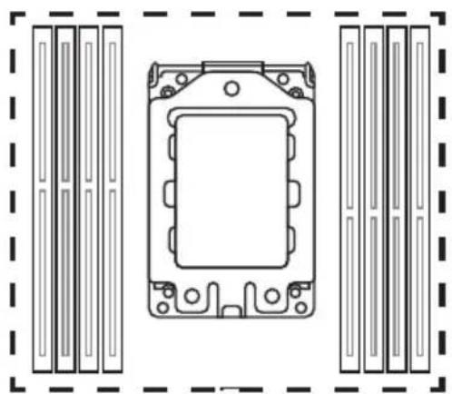
natural_image
Technical line drawing of a mechanical component with mounting holes and internal cavity (no text or symbols)D2 D1 C2 C1 A1 A2 B1 B2
メモリモジュールの推奨取付順 序

natural_image
Technical line drawing of a mechanical assembly with fan blades and a flat plate (no text or symbols)natural_image
Diagram of a computer motherboard showing slots, connectors, and a central CPU socket (no text or labels)| 1 5 4 8 CPU_PWR1/ CPU_PWR2 | |||
| 1 Ground 5 | +12V | ||
| 2 Ground 6 | +12V | ||
| 3 Ground 7 | +12V | ||
| 4 Ground 8 | +12V | ||
| 12 24ATX_PWR11 13 | 1 +3.3V 13 +3.3V | ||
| 2 +3.3V 14 -12V | |||
| 3 Ground 15 Ground | |||
| 4 +5V 16 PS-ON# | |||
| 5 Ground 17 Ground | |||
| 6 +5V 18 Ground | |||
| 7 Ground 19 Ground | |||
| 8 PWR OK 20 Res | |||
| 9 5VSB 21 | +5V | ||
| 10 +12V 22 +5V | |||
| 11 +12V 23 +5V | |||
| 12 +3.3V 24 Ground |

注意
natural_image
Diagram showing a blue curved shape inside a circle with a black triangular cutout and a red arrow indicating direction (no text or symbols)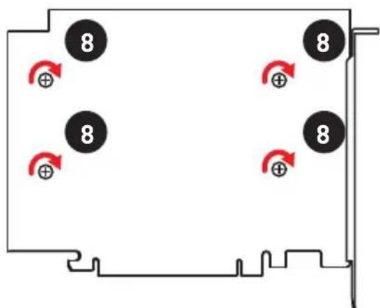
natural_image
Diagram of a computer motherboard showing CPU socket, RAM slots, and memory card (no text or labels)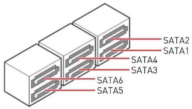

natural_image
Diagram of a computer motherboard showing CPU socket, RAM slots, and connectors (no text or labels)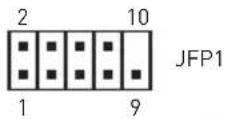 | |||
| 1 | HDD LED + | 2 | Power LED + |
| 3 | HDD LED - | 4 | Power LED - |
| 5 | Reset Switch | 6 | Power Switch |
| 7 | Reset Switch | 8 | Power Switch |
| 9 | Reserved | 10 | No Pin |
1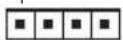 JFP2 JFP2 | 1 | Speaker - | 2 | Buzzer + |
| 3 | Buzzer - | 4 | Speaker + |
natural_image
Diagram of a computer motherboard showing slots, connectors, and a highlighted component (no text or labels)| 2 10 | |||
| 1 VCC 2 VCC | |||
| 3 USB0- 4 USB1- | |||
| 5 USB0+ 6 USB1+ | |||
| 7 Ground 8 Ground | |||
| 9 No Pin 10 NC | |||

natural_image
Diagram of a computer motherboard showing CPU socket, RAM slots, and memory drive (no text or labels)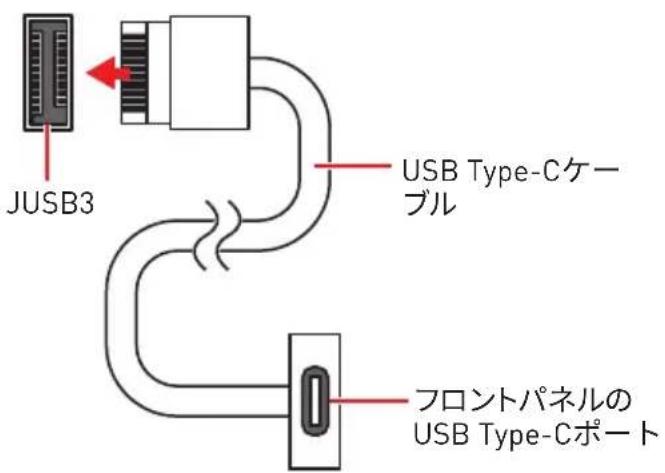
natural_image
Diagram of a computer motherboard showing slots, connectors, and a highlighted component (no text or labels)| 1 Power 11 USB2.0+ | |||
| 2 | USB3_RX_DN | 12 | USB2.0- |
| 3 | USB3_RX_DP | 13 | Ground |
| 4 | Ground | 14 | USB3_TX_C_DP |
| 5 | USB3_TX_C_DN | 15 | USB3_TX_C_DN |
| 6 | USB3_TX_C_DP | 16 | Ground |
| 7 | Ground | 17 | USB3_RX_DP |
| 8 | USB2.0- | 18 | USB3_RX_DN |
| 9 | USB2.0+ | 19 | Power |
| 10 | NC | 20 | No Pin |

natural_image
Diagram of a computer motherboard layout showing slots, connectors, and a highlighted component (no text or labels)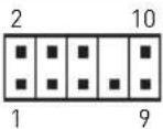 | |||
| 1 MIC L 2 | Ground | ||
| 3 MIC R 4 NC | |||
| 5 | Head Phone R | 6 | MIC Detection |
| 7 | SENSE_SEND | 8 | No Pin |
| 9 | Head Phone L | 10 | Head Phone Detection |
natural_image
Diagram of a computer motherboard showing CPU socket, RAM slots, and drive bays (no text or labels)
CPU FAN1/ EXS FAN1/
EXS FAN2/SYS FAN2/
SYS_FAN3/ SYS_FAN4
line
| Smart Fan Mode | Temperature Source | |---|---| | 85°C/185F/ | 100% | | 79°C/158F/ | 63% | | 55°C/131F/ | 38% | | 49°C/104F/ | 13% |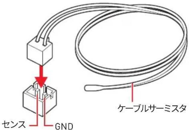
natural_image
Diagram of a computer motherboard showing slots, connectors, and a highlighted component (no text or labels)natural_image
Diagram of a computer motherboard layout showing slots, connectors, and a highlighted CPU socket (no text or labels)
リセットボタン
電源ボタン
natural_image
Diagram of a computer motherboard showing CPU socket, RAM slots, and memory drive (no text or labels)2 14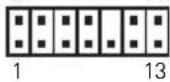 | |||
| 1 LPC Clock 2 3V Standby power | |||
| 3 LPC Reset 4 3.3V Power | |||
| 5 | LPC address & data pin0 | 6 | Serial IRQ |
| 7 | LPC address & data pin1 | 8 | 5V Power |
| 9 | LPC address & data pin2 | 10 | No Pin |
| 11 | LPC address & data pin3 | 12 | Ground |
| 13 | LPC Frame | 14 | Ground |
natural_image
Diagram of a computer motherboard layout showing slots, CPU socket, and indicator lights (no text or labels)
データを保持 (デフォルト)

CMOSをクリア/ BIOSをリセット
BIO Sをデフォルト値にリセットする

正常
(デフォルト)

ケース開放イベント
リガー有効
ケース開放検知機能の使い方
natural_image
Diagram of a computer motherboard layout showing CPU socket, RAM slots, and memory card (no text or labels)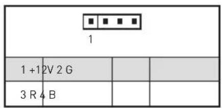
RGB LEDストリップコネクター
natural_image
Diagram of a computer motherboard showing slots, connectors, and CPU socket (no text or labels)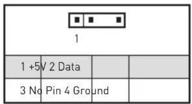
natural_image
Diagram of a computer motherboard showing CPU socket, RAM slots, and connectors (no text or labels)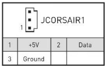
natural_image
Diagram of a computer motherboard layout showing slots, connectors, and a highlighted component (no text or labels)JOC_RT1

正常
(デフォルト)
JOC_FS1

正常
(デフォルト)

OCを再試行し
続ける

OC-FAILメッセージ
を表示せずにBIOS
に入って強制される
natural_image
Diagram of a computer motherboard showing CPU socket, RAM slots, and memory drive components (no text or labels)
正常
(デフォルト)

有効
natural_image
Diagram of a computer motherboard layout showing CPU socket, RAM slots, and drive bays (no text or labels)
▶ Advanced CPU Configuration
▶ Memory Failure Retry
▶ CPU Voltages control [Auto]
▶ Memory Changed Detect [Enabled]\*
▶ CPU Specifications
▶ CPU Technology Support
natural_image
Diagram showing a headset connected to an audio jack via a cable, with no text or symbols present.스테레오 스피커용 오디오 잡 도표
3.안테나를 최대한 높이 돕니다.
natural_image
Isometric line drawing of a desktop computer setup with monitor, keyboard, tower, and wireless signal waves (no text or symbols)구성품 개요
CPU 소켓
natural_image
Diagram of a computer motherboard showing slots and CPU socket (no text or labels)natural_image
Mechanical assembly diagram showing a CPU cooling unit with red arrows indicating rotational direction (no text or symbols present)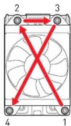
natural_image
Diagram showing a heat exchanger with cooling fins and a base-mounted circuit board (no text or symbols)종요사항
natural_image
Diagram of a computer motherboard showing two rows of connectors and slots (no text or labels)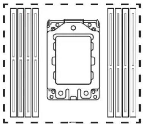
natural_image
Technical line drawing of a mechanical component with mounting holes and internal cavity (no text or symbols)D2 D1 C2 C1 A1 A2 B1 B2
메모리 모듈 설치 추천

natural_image
Technical line drawing of a mechanical assembly with fan blades and a flat plate (no text or symbols)natural_image
Diagram of a computer motherboard showing slots, connectors, and a central CPU socket (no text or labels)| 1 5 4 8 CPU_PWR1/ CPU_PWR2 | |||
| 1 Ground 5 | +12V | ||
| 2 Ground 6 | +12V | ||
| 3 Ground 7 | +12V | ||
| 4 Ground 8 | +12V | ||
| 12 24ATX_PWR11 13 | 1 +3.3V 13 +3.3V | ||
| 2 +3.3V 14 -12V | |||
| 3 Ground 15 Ground | |||
| 4 +5V 16 PS-ON# | |||
| 5 Ground 17 Ground | |||
| 6 +5V 18 Ground | |||
| 7 Ground 19 Ground | |||
| 8 PWR OK 20 Res | |||
| 9 5VSB 21 +5V | |||
| 10 +12V 22 +5V | |||
| 11 +12V 23 +5V | |||
| 12 +3.3V 24 Ground |

중요사항
M.2 XPANDER-AERO GEN4 설치하기
natural_image
Diagram showing a blue arrow pointing to a circular shape with a number 7 in the top-left corner (no text or symbols on the arrow itself)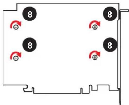
natural_image
Diagram of a computer motherboard showing CPU socket, RAM slots, and drive bays (no text or labels)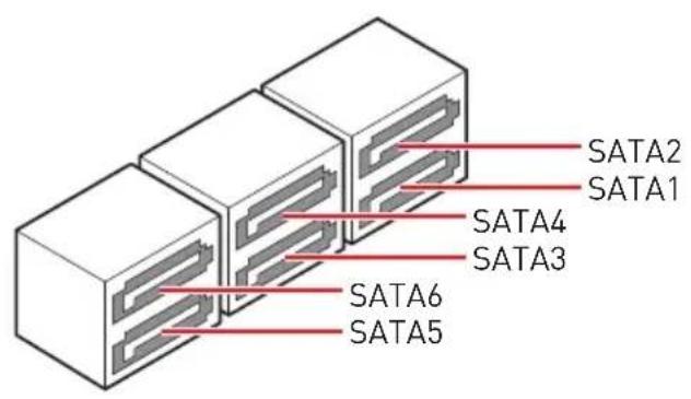

natural_image
Diagram of a computer motherboard showing CPU socket, RAM slots, and connectors (no text or labels) | |||
| 1 HDD LED + 2 Power LED + | |||
| 3 HDD LED - 4 Power LED - | |||
| 5 Reset Switch 6 Power Switch | |||
| 7 Reset Switch 8 Power Switch | |||
| 9 Reserved 10 No Pin | |||
| JFP2 | 1 Speaker - 2 Buzzer + | ||
| 3 Buzzer - 4 | Speaker + | ||
natural_image
Diagram of a computer motherboard showing slots, connectors, and a highlighted component (no text or labels)| 1 VCC 2 VCC | |||
| 3 USB0- 4 USB1- | |||
| 5 USB0+ 6 USB1+ | |||
| 7 Ground 8 Ground | |||
| 9 No Pin 10 NC | |||

natural_image
Diagram of a computer motherboard showing CPU socket, RAM slots, and memory card (no text or labels)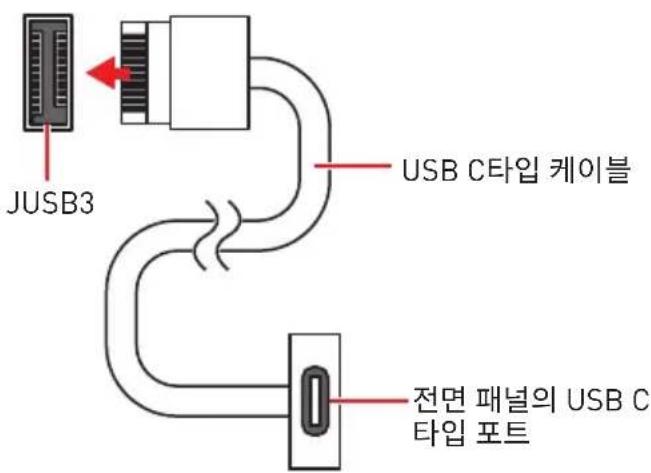
natural_image
Diagram of a computer motherboard showing CPU socket, RAM slots, and drive bays (no text or labels)| 10 11 20 | |||
| 1 Power 11 USB2.0+ | |||
| 2 USB3_RX_DN 12 USB2.0- | |||
| 3 USB3_RX_DP 13 Ground | |||
| 4 Ground 14 USB3_TX_C_DP | |||
| 5 | USB3_TX_C_DN | 15 | USB3_TX_C_DN |
| 6 | USB3_TX_C_DP | 16 Ground | |
| 7 Ground 17 USB3_RX_DP | |||
| 8 | USB2.0- | 18 | USB3_RX_DN |
| 9 | USB2.0+ | 19 | Power |
| 10 | NC | 20 | No Pin |

natural_image
Diagram of a computer motherboard showing CPU socket, RAM slots, and memory drive components (no text or labels) | |||
| 1 MIC L 2 Ground | |||
| 3 MIC R 4 NC | |||
| 5 Head Phone R | 6 | MIC Detection | |
| 7 SENSE_SEND 8 | No Pin | ||
| 9 Head Phone L 10 Head P | Phone | Detection | |
CPU\_FAN1, PUMP\_FAN1, SYS\_FAN1\~4, EXS\_FAN1\~3,: 팬 커넥터
PWM 모드 팬 커넥터 기본 설정
Auto 모드 팬 커넥터 기본 설정
팬 모드 전환 및 속도 조정
line
| Smart Fan Mode | Temperature Source | |---|---| | 85°C/185F/ | CPU | | 79°C/158F/ | CPU Fan1 step up time | | 55°C/131F/ | 0.1s | | 49°C/104F/ | 0.1s |natural_image
Diagram of a computer motherboard showing CPU socket, RAM slots, and drive bays (no text or labels)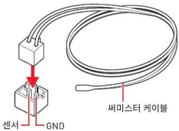
natural_image
Diagram of a computer motherboard showing slots, connectors, and a highlighted component (no text or labels)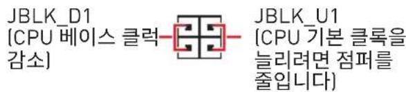
natural_image
Diagram of a computer motherboard showing slots, CPU socket, and indicator lights (no text or labels)
리셋 버튼
전원 버튼
JTPM1: TPM 모듈 커넥터
natural_image
Diagram of a computer motherboard showing CPU socket, RAM slots, and memory drive (no text or labels)| 2 14 | |||
| 1 LPC Clock 2 3V Standby power | |||
| 3 LPC Reset 4 3.3V Power | |||
| 5 LPC address & data pin0 6 Serial IRQ | |||
| 7 LPC address & data pin1 8 5V Power | |||
| 9 LPC address & data pin2 10 No Pin | |||
| 11 LPC address & data pin3 12 Ground | |||
| 13 | LPC Frame | 14 Ground | |
natural_image
Diagram of a computer motherboard layout showing slots, CPU socket, and connectors (no text or labels)
데이터 유지 (기본 설정)

CMOS 클리어/ BIOS 리셋
기본 값으로 BIOS 리셋하기
natural_image
Diagram of a computer motherboard showing CPU socket, RAM slots, and drive bays (no text or labels)
표준 상태 (기본 설정)

새시 침입 이벤트 트리거
새시 침입 탐지기 사용하기
natural_image
Diagram of a computer motherboard layout showing CPU socket, RAM slots, and memory card (no text or labels)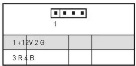
RGB LED 스트립 연결
natural_image
Diagram of a computer motherboard showing slots, connectors, and CPU socket (no text or labels)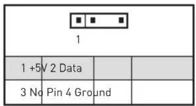
natural_image
Diagram of a computer motherboard showing CPU socket, RAM slots, and memory drive components (no text or labels)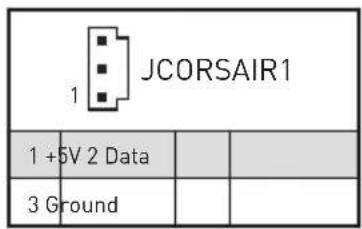
natural_image
Diagram of a computer motherboard layout showing slots, connectors, and a highlighted component (no text or labels)JOC_RT1

표준 상태
(기본 설정)

OC 재시도
JOC_FS1

표준 상태
(기본 설정)

BIOS로 강제
진입
natural_image
Diagram of a computer motherboard showing CPU socket, RAM slots, and memory drive components (no text or labels)
표준 상태
(기본 설정)

활성화
natural_image
Diagram of a computer motherboard layout showing slots, connectors, and a highlighted component (no text or labels)EZ 모드
종요사항
▶ Advanced CPU Configuration
▶ Memory Failure Retry
▶ CPU Voltages control [Auto]
▶ Memory Changed Detect [Enabled]\*
▶ CPU Specifications
▶ CPU Technology Support
▶ Spread Spectrum (optional)
JBLK_D1, JBLK_U1: 基頻增減接頭....32
natural_image
Diagram showing a headset connected to an audio jack via a cable, with no text or symbols present.連接立體聲喇叭插孔示意圖
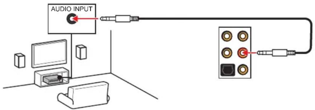
連接 7.1 聲道喇叭插孔示意圖
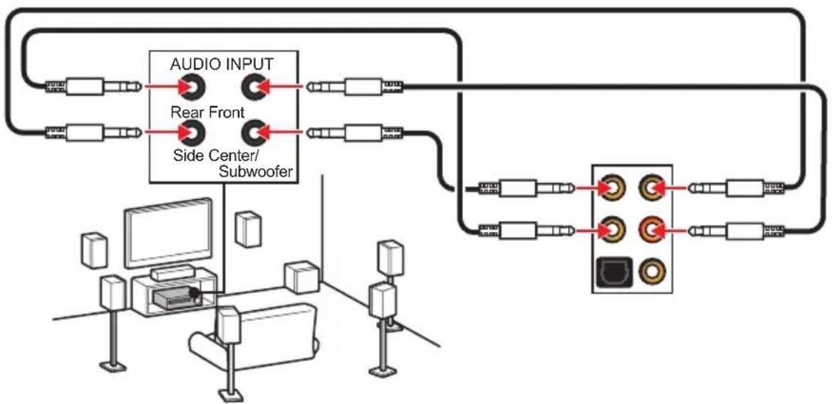
flowchart
graph TD
    A["Audio Input"] --> B["Rear Front"]
    B --> C["Side Center/Subwoofer"]
    C --> D["Output Module 1"]
    C --> E["Output Module 2"]
    C --> F["Output Module 3"]
    C --> G["Output Module 4"]
安裝天線
- 盡量將天線放置在高處。
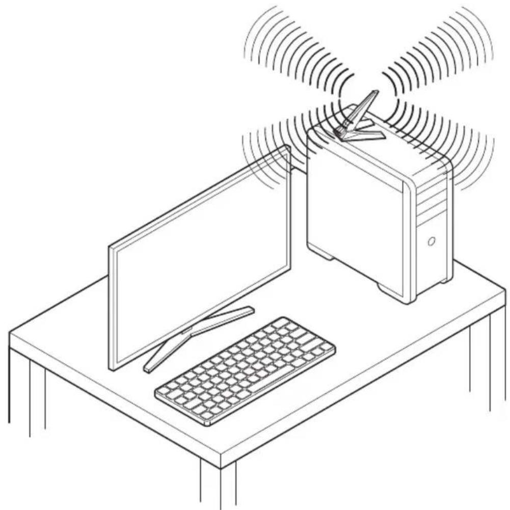
natural_image
Isometric line drawing of a desktop computer setup with monitor, keyboard, tower, and wireless signal waves (no text or symbols)元件總覽
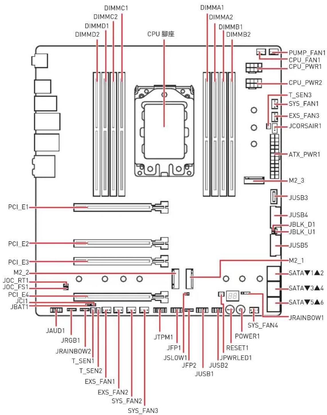
處理器腳座
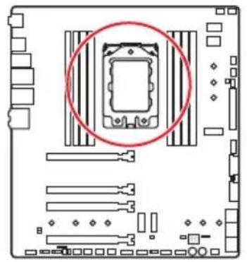
natural_image
Diagram of a computer motherboard showing slots, connectors, and a highlighted component (no text or labels)natural_image
Mechanical assembly diagram showing a CPU cooling unit with red arrows indicating rotational direction (no text or symbols present)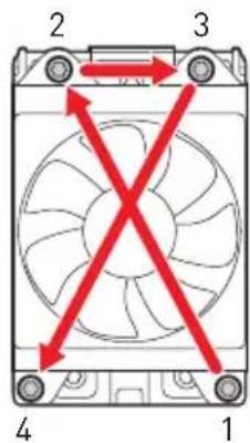
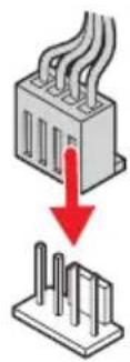

natural_image
Diagram of a computer motherboard showing two rows of slots and connectors (no text or labels)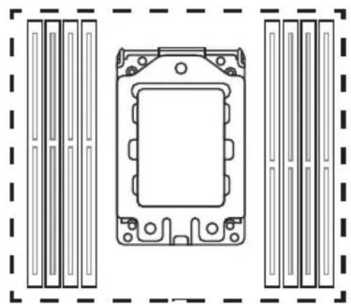
natural_image
Technical line drawing of a mechanical component with mounting holes and internal cavity (no text or symbols)D2 D1 C2 C1 A1 A2 B1 B2
記憶體模組安裝建議
| D2 D1 C2 C1 CPU 腳座 A1 A2 B1 B2 | |||||||||
| 1 DIMM | 第三代 AMD RyzenTM ThreadripperTM 桌上型處理器 | √ | |||||||
| 2 DIMMs | √ | √ | |||||||
| 4 DIMMs | √ | √ | √ | √ | |||||
| 8 DIMMs | √ | √ | √ | √ | √ | √ | √ | √ | |
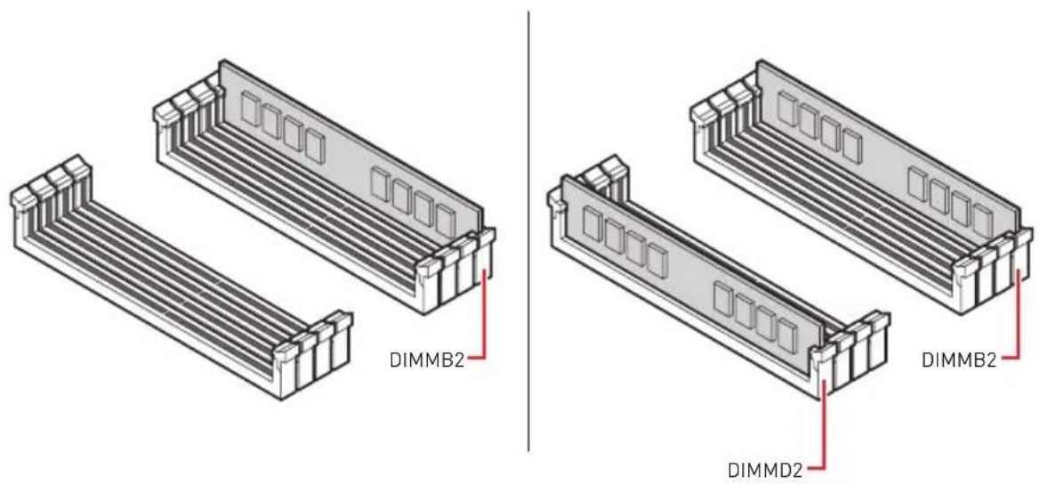
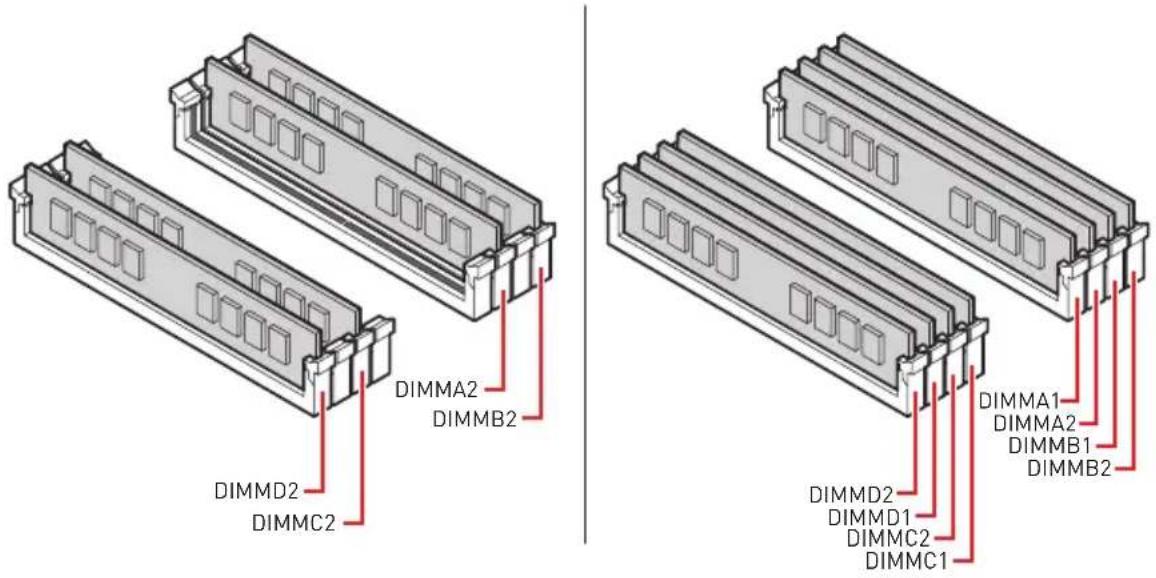

natural_image
Technical line drawing of a mechanical assembly with cooling fans and a flat panel, showing no text or symbols.CPU\_PWR1\~2, ATX\_PWR1: 電源接頭
natural_image
Diagram of a computer motherboard showing slots, connectors, and memory slots (no text or labels)| 1 5 4 8 CPU_PWR1/ CPU_PWR2 | |||
| 1 Ground 5 | +12V | ||
| 2 Ground 6 | +12V | ||
| 3 Ground 7 | +12V | ||
| 4 Ground 8 | +12V | ||
| 12 24 13 ATX_PWR1 | 1 +3.3V 13 +3.3V | ||
| 2 +3.3V 14 -12V | |||
| 3 Ground 15 Ground | |||
| 4 +5V 16 PS-ON# | |||
| 5 Ground 17 Ground | |||
| 6 +5V 18 Ground | |||
| 7 Ground 19 Ground | |||
| 8 PWR OK 20 Res | |||
| 9 5VSB 21 +5V | |||
| 10 +12V 22 +5V | |||
| 11 +12V 23 +5V | |||
| 12 +3.3V 24 Ground |

重要
natural_image
Diagram showing a blue curved shape with a red arrow inside, enclosed in a circle (no text or symbols)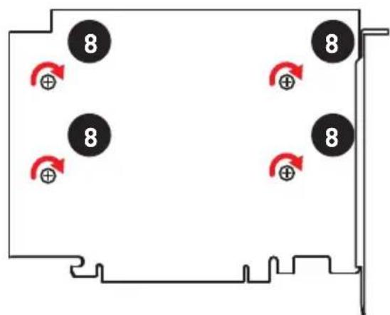
natural_image
Diagram of a computer motherboard showing CPU socket, RAM slots, and memory card (no text or labels)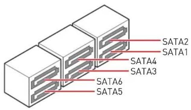

natural_image
Diagram of a computer motherboard showing CPU socket, RAM slots, and memory drive layout (no text or labels)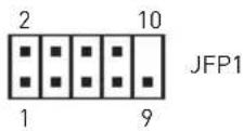 | |||
| 1 HDD LED + 2 Power LED + | |||
| 3 HDD LED - 4 Power LED - | |||
| 5 Reset Switch 6 Power Switch | |||
| 7 Reset Switch 8 Power Switch | |||
| 9 Reserved 10 No Pin | |||
1 JFP2 JFP2 | 1 Speaker - 2 | Buzzer + | |
| 3 Buzzer - 4 | Speaker + |
natural_image
Diagram of a computer motherboard showing slots, connectors, and a highlighted component (no text or labels)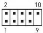 | |||
| 1 VCC 2 VCC | |||
| 3 USB0- 4 USB1- | |||
| 5 USB0+ 6 USB1+ | |||
| 7 Ground 8 Ground | |||
| 9 No Pin 10 NC | |||

natural_image
Diagram of a computer motherboard showing CPU socket, RAM slots, and memory card (no text or labels)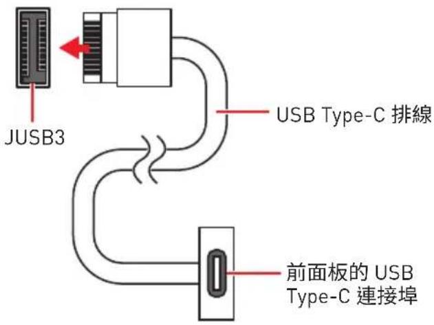
natural_image
Diagram of a computer motherboard showing CPU socket, RAM slots, and drive bays (no text or labels)| 10 11 20 | |||
| 1 Power 11 USB2.0+ | |||
| 2 USB3_RX_DN 12 USB2.0- | |||
| 3 USB3_RX_DP 13 Ground | |||
| 4 Ground 14 USB3_TX_C_DP | |||
| 5 USB3_TX_C_DN | 15 | USB3_TX_C_DN | |
| 6 USB3_TX_C_DP | 16 Ground | ||
| 7 Ground 17 USB3_RX_DP | |||
| 8 USB2.0- | 18 | USB3_RX_DN | |
| 9 USB2.0+ | 19 | Power | |
| 10 NC | 20 | No Pin | |

natural_image
Diagram of a computer motherboard showing CPU socket, RAM slots, and drive bays (no text or labels)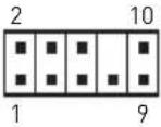 | |||
| 1 MIC L 2 Ground | |||
| 3 MIC R 4 NC | |||
| 5 Head Phone R | 6 | MIC Detection | |
| 7 SENSE_SEND | 8 | No Pin | |
| 9 Head Phone L 10 | Head Phone Detection | ||
CPU\_FAN1, PUMP\_FAN1, SYS\_FAN1\~4, EXS\_FAN1\~3: 風扇電源接頭
natural_image
Diagram of a computer motherboard showing slots, connectors, and memory layout (no text or labels)line
| Smart Fan Mode | Temperature Source | |---|---| | 85°C/185F/ | 100% | | 79°C/158F/ | 63% | | 55°C/131F/ | 38% | | 49°C/104F/ | 13% |natural_image
Diagram of a computer motherboard showing CPU socket, RAM slots, and drive bays (no text or labels)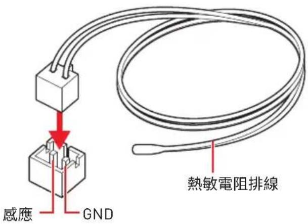
natural_image
Diagram of a computer motherboard showing slots, connectors, and a highlighted component (no text or labels)![JBLK_D1 [減少 CPU 基頻] - [ ] - [增加 CPU 基頻] JBLK_U1](/content/2026/05/877918/images/b6c625411c0a1744c92e5ec80fad08340d473b9132d2730fda4a51f463c746f3.jpg)
natural_image
Diagram of a computer motherboard showing slots, connectors, and a highlighted CPU socket (no text or labels)
重新開機按鈕
電源按鈕
JTPM1: TPM 模組接頭
natural_image
Diagram of a computer motherboard showing slots, CPU socket, and memory drive (no text or labels)| 2 14 | |||
| 1 LPC Clock 2 3V Standby power | |||
| 3 LPC Reset 4 3.3V Power | |||
| 5 LPC address & data pin0 6 Serial IRQ | |||
| 7 LPC address & data pin1 8 5V Power | |||
| 9 LPC address & data pin2 10 No Pin | |||
| 11 LPC address & data pin3 12 | Ground | ||
| 13 | LPC Frame | 14 | Ground |
natural_image
Diagram of a computer motherboard showing slots, CPU socket, and connectors (no text or labels)
保留資料 (預設值)

清除 CMOS/ 重置 BIOS
重設 BIOS 為預設值
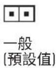
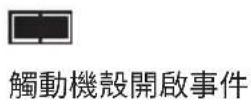
使用機殼開啟偵測器
natural_image
Diagram of a computer motherboard layout showing CPU socket, RAM slots, and memory card (no text or labels)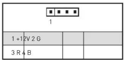
RGB LED 燈條連接示意圖

natural_image
Diagram of a computer motherboard showing slots, connectors, and CPU socket (no text or labels)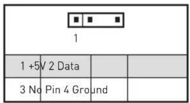
可定址 RGB LED 燈條連接示意圖
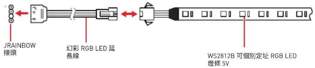
natural_image
Diagram of a computer motherboard showing CPU socket, RAM slots, and memory drive components (no text or labels)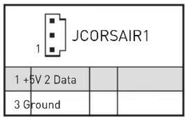
CORSAIR RGB 風扇連接示意圖
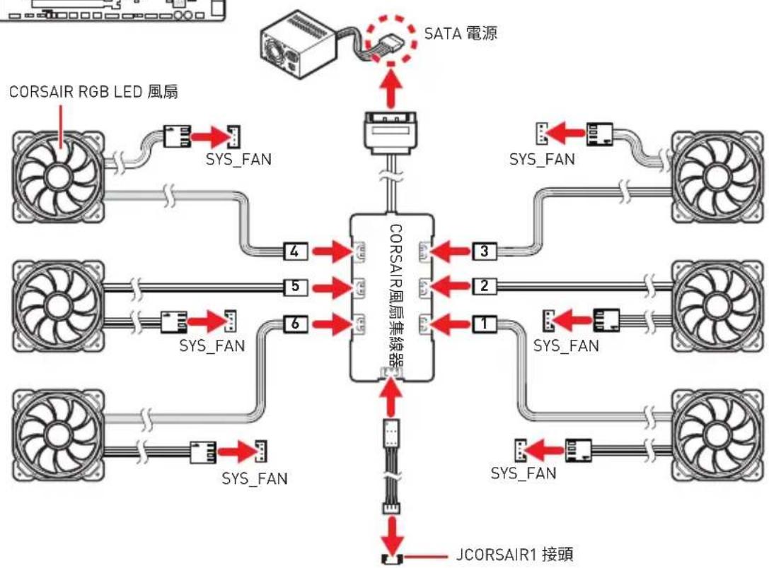
flowchart
graph TD
    A["SATA 電源"] --> B["CPU"]
    B --> C["CORSAIR 固相采集器"]
    C --> D["JSYS_FAN"]
    C --> E["JSYS_FAN"]
    C --> F["JSYS_FAN"]
    C --> G["JSYS_FAN"]
    C --> H["JCORSAIR1 接頭"]
    I["CORSAIR RGB LED 風扇"] --> J["sys_FAN"]
    K["JSYS_FAN"] --> L["sys_FAN"]
    M["JSYS_FAN"] --> N["sys_FAN"]
    O["JSYS_FAN"] --> P["sys_FAN"]
    Q["JSYS_FAN"] --> R["sys_FAN"]
    S["JSYS_FAN"] --> T["sys_FAN"]
    U["JSYS_FAN"] --> V["sys_FAN"]
    W["JSYS_FAN"] --> X["sys_FAN"]
    Y["JSYS_FAN"] --> Z["sys_FAN"]
    AA["JSYS_FAN"] --> AB["sys_FAN"]
    AC["JSYS_FAN"] --> AD["sys_FAN"]
    AE["JSYS_FAN"] --> AF["sys_FAN"]
    AG["JSYS_FAN"] --> AH["sys_FAN"]
    AI["JSYS_FAN"] --> AJ["sys_FAN"]
    AK["JSYS_FAN"] --> AL["sys_FAN"]
    AM["JSYS_FAN"] --> AN["sys_FAN"]
    AO["JSYS_FAN"] --> AP["sys_FAN"]
    AQ["JSYS_FAN"] --> AR["sys_FAN"]
    AS["JSYS_FAN"] --> AT["sys_FAN"]
    AU["JSYS_FAN"] --> AV["sys_FAN"]
    AW["JSYS_FAN"] --> AX["sys_FAN"]
    AY["SATA 電源"] --> AZ["CPU"]
    BA["JCORSAIR1 接頭"] --> BB["CSAAR 固相采集器"]
natural_image
Diagram of a computer motherboard layout showing slots, connectors, and a highlighted component (no text or labels)JOC_RT1

一般
(預設值)
JOC_FS1

一般
(預設值)

OC 重試

強制進入 BIOS
JSLOW1: 低速模式啟動跳線
natural_image
Diagram of a computer motherboard showing slots, CPU socket, and indicator lights (no text or labels)
一般
(預設值)

啟用
natural_image
Diagram of a computer motherboard layout showing slots, connectors, and a highlighted component (no text or labels)natural_image
Diagram of a computer motherboard layout showing CPU socket, RAM slots, and drive bays (no text or labels)JPWRLED1 - LED 電源輸入
除錯碼 LED
EZ 模式

▶ Advanced CPU Configuration
▶ Memory Failure Retry
▶ Memory Changed Detect [Enabled]\*
▶ CPU Specifications
▶ CPU Technology Support
JBLK_D1, JBLK_U1: 基频增减接头.....32
POWER1, RESET1: 电源按钮, 重启按钮 ..... 32
JTPM1: TPM 模组接口 33
JBAT1: 清除 CMOS (重启 BIOS) 跳线..... 33
JCI1: 机箱入侵检测接口.....34
natural_image
Diagram showing a headset connected to an audio jack via a cable, with no text or symbols present.立体声喇叭至音频插孔示意图
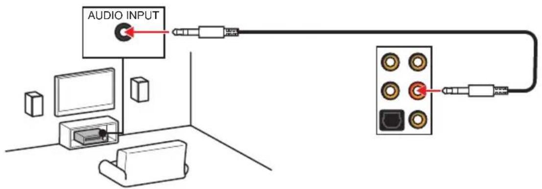
7.1-声道喇叭至音频插孔示意图
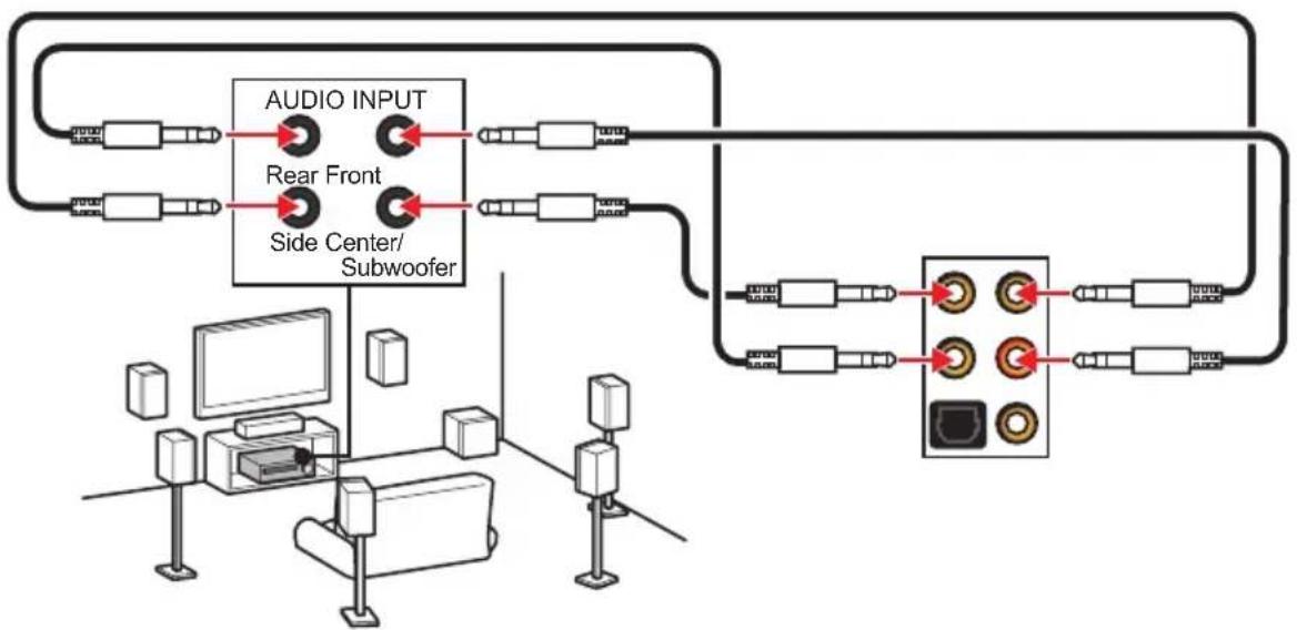
flowchart
graph TD
    A["Audio Input"] --> B["Rear Front"]
    B --> C["Side Center/Subwoofer"]
    C --> D["Output Module 1"]
    C --> E["Output Module 2"]
    C --> F["Output Module 3"]
    C --> G["Output Module 4"]
安装天线
- 请将天线尽量放置更高。
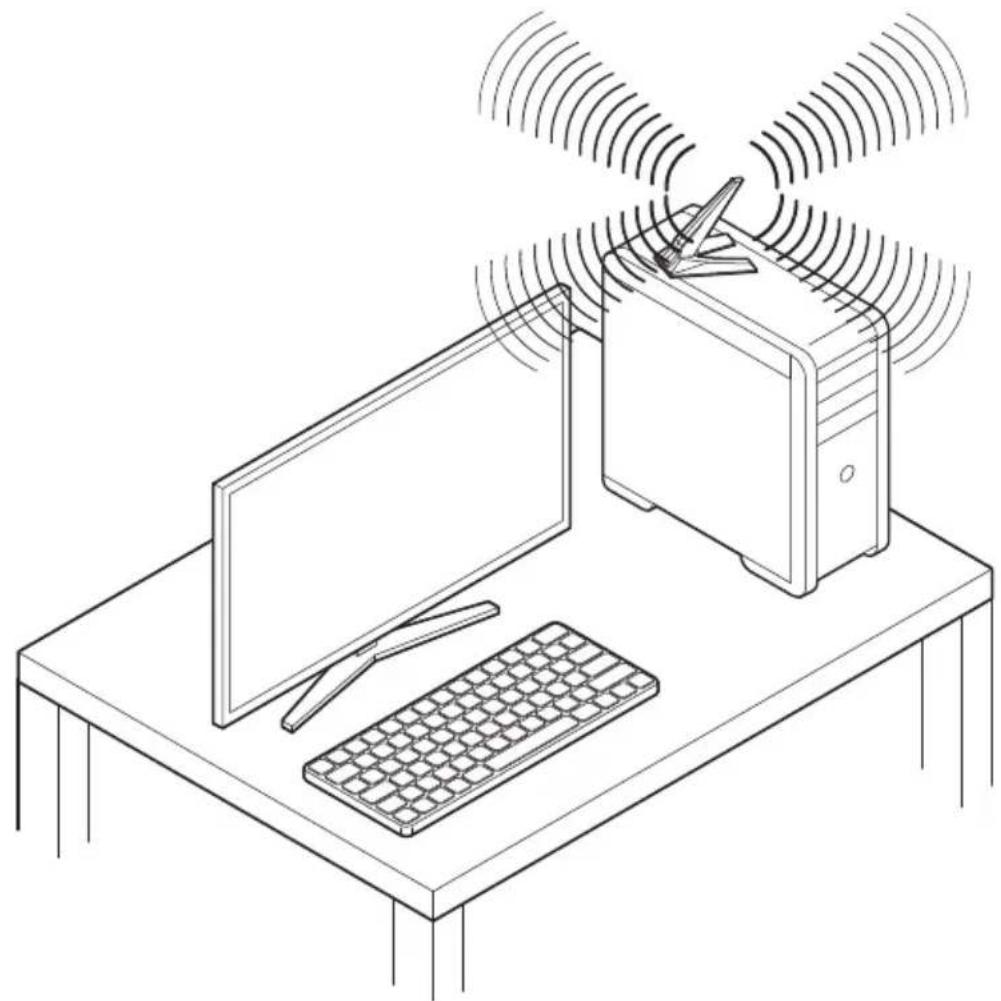
natural_image
Isometric line drawing of a desktop computer setup with monitor, keyboard, tower, and wireless signal waves (no text or symbols)组件概述
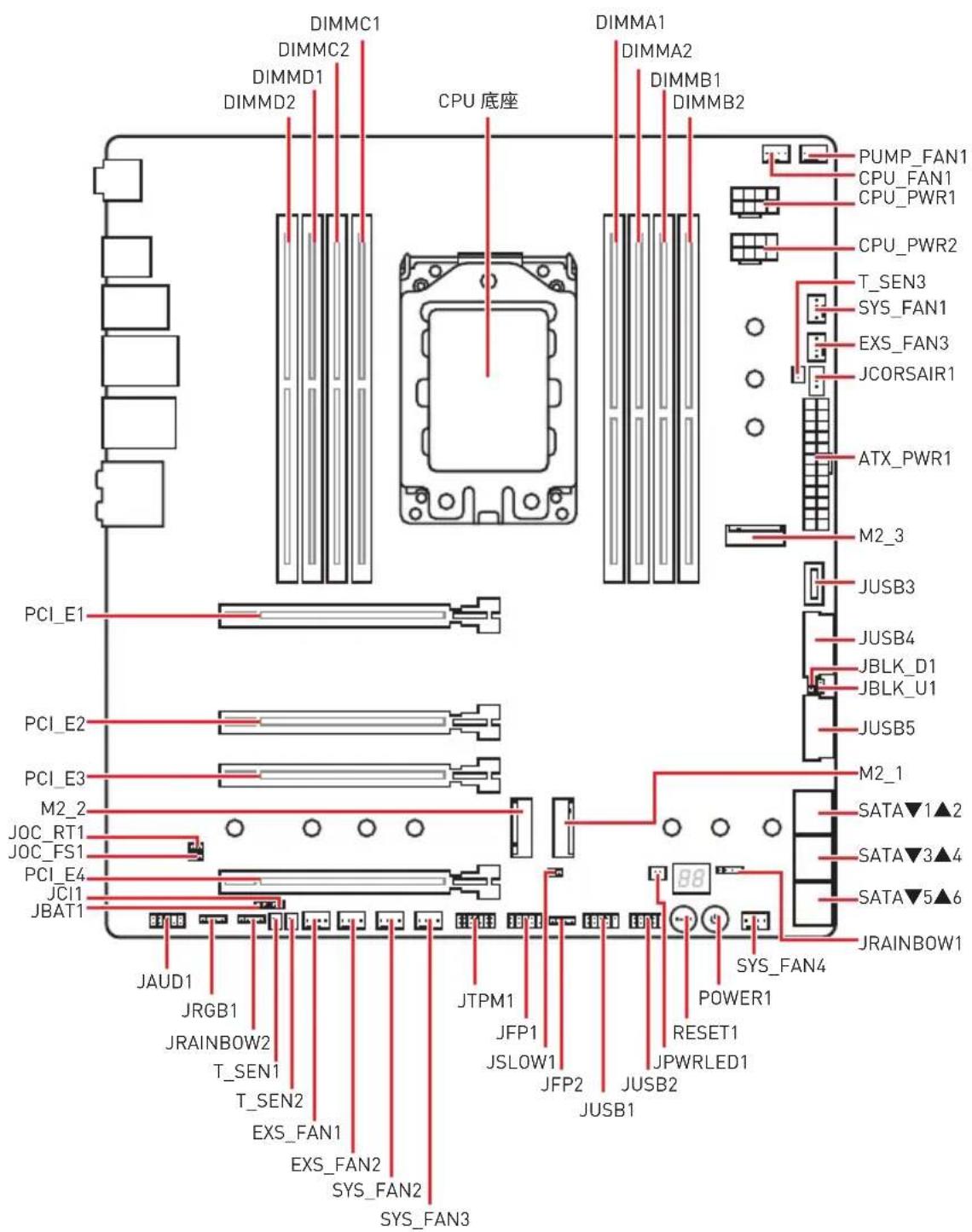
CPU 底座
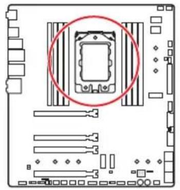
natural_image
Diagram of a computer motherboard showing slots, connectors, and a highlighted component (no text or labels)natural_image
Diagram of a computer motherboard showing two rows of slots and connectors (no text or labels)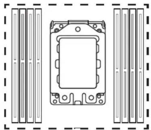
natural_image
Technical line drawing of a mechanical component with mounting holes and internal cavity (no text or symbols)D2 D1 C2 C1 A1 A2 B1 B2
内存模块安装建议
| D2 D1 C2 C1 CPU 底座 A1 A2 B1 B2 | |||||||||
| 1 DIMM | 第三代 AMD 锐龙TM ThreadripperTM 台式机处理器 | √ | |||||||
| 2 DIMMs | √ | √ | |||||||
| 4 DIMMs | √ | √ | √ | √ | |||||
| 8 DIMMs | √ | √ | √ | √ | √ | √ | √ | √ | |
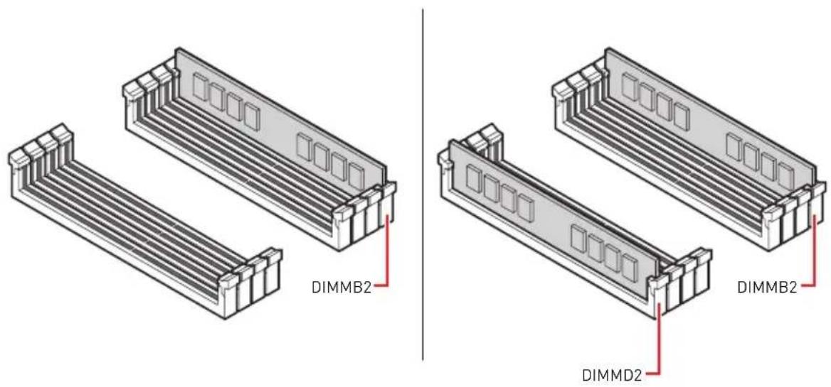
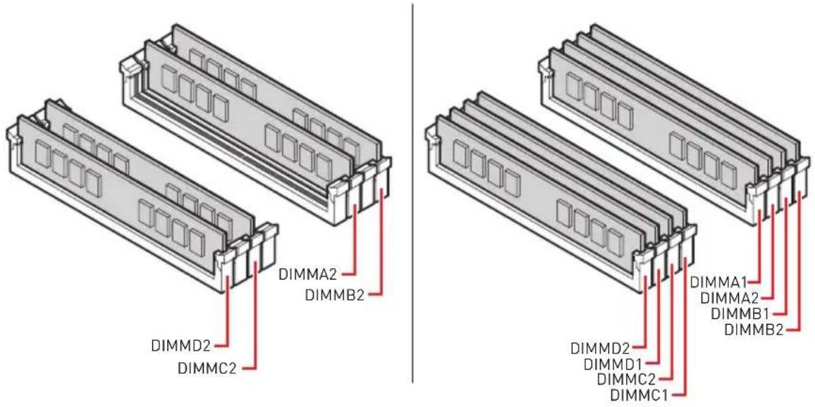

natural_image
Technical line drawing of a mechanical fan assembly with cooling fins and a flat cover (no text or symbols)CPU\_PWR1\~2, ATX\_PWR1: 电源接口
natural_image
Diagram of a computer motherboard showing slots, connectors, and memory slots (no text or labels)| 1 5 4 8 CPU_PWR1/ CPU_PWR2 | |||
| 1 Ground 5 | +12V | ||
| 2 Ground 6 | +12V | ||
| 3 Ground 7 | +12V | ||
| 4 Ground 8 | +12V | ||
| 12 24ATX_PWR11 13 | 1 +3.3V 13 +3.3V | ||
| 2 +3.3V 14 -12V | |||
| 3 Ground 15 Ground | |||
| 4 +5V 16 PS-ON# | |||
| 5 Ground 17 Ground | |||
| 6 +5V 18 Ground | |||
| 7 Ground 19 Ground | |||
| 8 PWR OK 20 Res | |||
| 9 5VSB 21 +5V | |||
| 10 +12V 22 +5V | |||
| 11 +12V 23 +5V | |||
| 12 +3.3V 24 Ground |

注意
http://v.youku.com/v_show/id_XNzUyMTY3MjY4.html
安装 M.2 模块
natural_image
Diagram showing a blue curved shape inside a circle with a red arrow, labeled with number 7 (no text or symbols on the shape itself)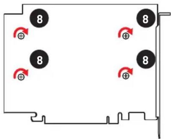
natural_image
Diagram of a computer motherboard showing CPU socket, RAM slots, and connectors (no text or labels)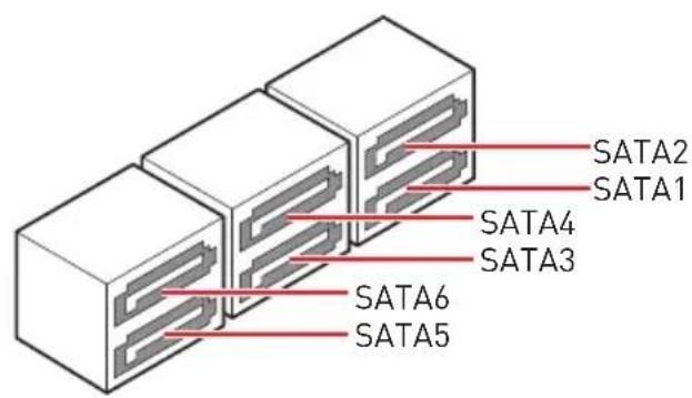

natural_image
Diagram of a computer motherboard showing slots, CPU socket, and indicator lights (no text or labels)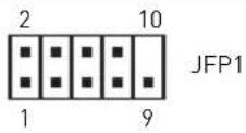 | |||
| 1 HDD LED + 2 Power LED + | |||
| 3 HDD LED - 4 Power LED - | |||
| 5 Reset Switch 6 Power Switch | |||
| 7 Reset Switch 8 Power Switch | |||
| 9 Reserved 10 No Pin | |||
| 1JFP2 | 1 Speaker - 2 Buzzer + | |||
| 3 Buzzer - 4 | Speaker + | |||
natural_image
Diagram of a computer motherboard showing slots, connectors, and a highlighted component (no text or labels)| 2 10 | |||
| 1 VCC 2 VCC | |||
| 3 USB0- 4 USB1- | |||
| 5 USB0+ 6 USB1+ | |||
| 7 Ground 8 Ground | |||
| 9 No Pin 10 NC | |||

natural_image
Diagram of a computer motherboard showing CPU socket, RAM slots, and drive bays (no text or labels)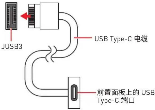
natural_image
Diagram of a computer motherboard showing slots, CPU socket, and memory drive components (no text or labels)| 10 11 20 | |||
| 1 Power 11 USB2.0+ | |||
| 2 USB3_RX_DN 12 USB2.0- | |||
| 3 USB3_RX_DP 13 Ground | |||
| 4 Ground 14 USB3_TX_C_DP | |||
| 5 USB3_TX_C_DN | 15 | USB3_TX_C_DN | |
| 6 USB3_TX_C_DP | 16 Ground | ||
| 7 Ground 17 USB3_RX_DP | |||
| 8 USB2.0- | 18 | USB3_RX_DN | |
| 9 USB2.0+ | 19 | Power | |
| 10 NC | 20 | No Pin | |

natural_image
Diagram of a computer motherboard showing CPU socket, RAM slots, and memory drive layout (no text or labels)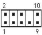 | |||
| 1 MIC L 2 Ground | |||
| 3 MIC R 4 NC | |||
| 5 Head Phone R | 6 | MIC Detection | |
| 7 SENSE_SEND | 8 | No Pin | |
| 9 Head Phone L 10 | Head Phone Detection | ||
CPU\_FAN1, PUMP\_FAN1, SYS\_FAN1\~4, EXS\_FAN1\~3,: 风扇接口
默认 PWM 模式风扇接口
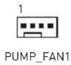
默认自动模式风扇接口
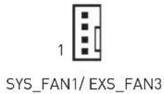
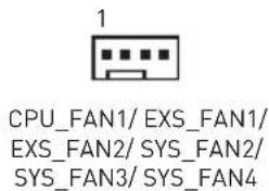
切换风扇模式和调整风扇速率
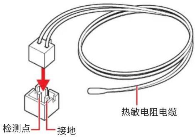
JBLK\_D1, JBLK\_U1: 基频增减接头
natural_image
Diagram of a computer motherboard layout showing slots, connectors, and a highlighted button (no text or labels)JBLK_D1 [减少 CPU 基频] JBLK_U1 [增加 CPU 基频]
POWER1, RESET1: 电源按钮,重启按钮
natural_image
Diagram of a computer motherboard showing slots, connectors, and a highlighted component (no text or labels)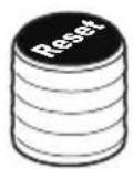
重启按钮
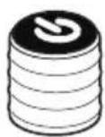
电源按钮
JTPM1: TPM 模组接口
natural_image
Diagram of a computer motherboard showing CPU socket, RAM slots, and memory drive (no text or labels)2 14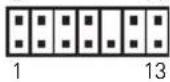 | |||
| 1 LPC Clock 2 3V Standby power | |||
| 3 LPC Reset 4 3.3V Power | |||
| 5 LPC address & data pin0 6 Serial IRQ | |||
| 7 LPC address & data pin1 8 5V Power | |||
| 9 LPC address & data pin2 10 | No Pin | ||
| 11 LPC address & data pin3 12 | Ground | ||
| 13 | LPC Frame | 14 | Ground |
JBAT1: 清除 CMOS (重启 BIOS) 跳线
natural_image
Diagram of a computer motherboard layout showing slots, connectors, and CPU socket (no text or labels)
保留数据 (默认)

清除 CMOS/重启 BIOS
重启 BIOS 为默认值

正常
[默认]

启用机箱入侵检测
使用机箱入侵检测器
natural_image
Diagram of a computer motherboard layout showing CPU socket, RAM slots, and memory card (no text or labels)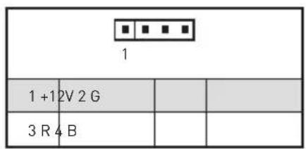
RGB LED 灯条连接

RGB LED 风扇连接
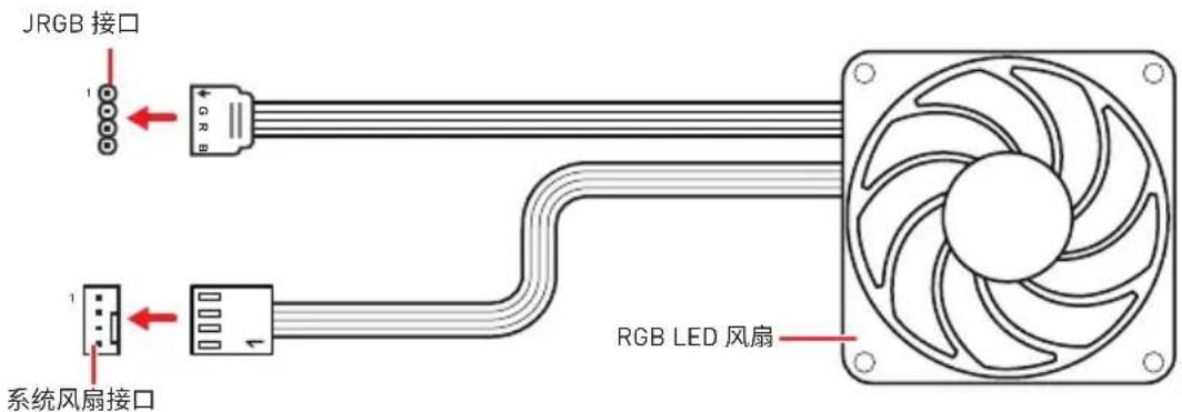
natural_image
Diagram of a computer motherboard showing slots, connectors, and CPU socket (no text or labels)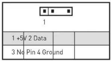
寻址 RGB LED 灯条连接
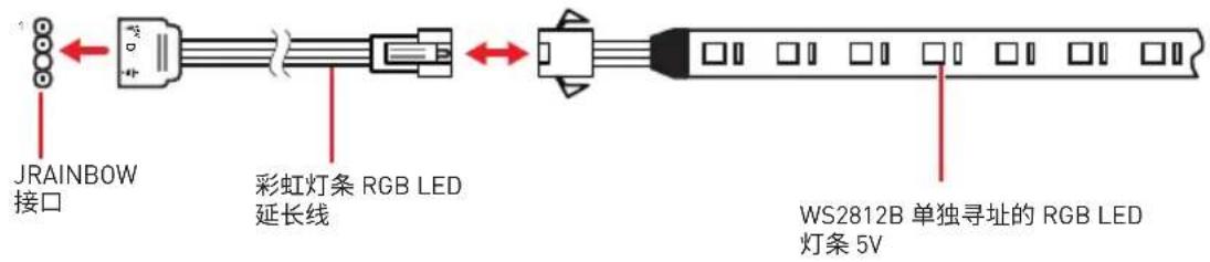
natural_image
Diagram of a computer motherboard showing slots, connectors, and a highlighted component (no text or labels)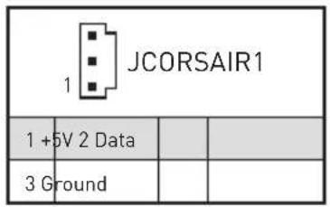
CORSAIR RGB LED 风扇连接
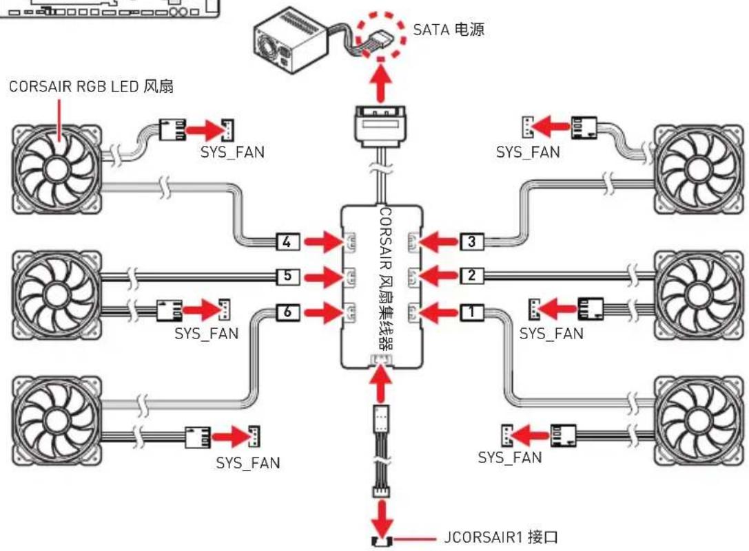
flowchart
graph TD
    A["SATA 电源"] --> B["CPU"]
    B --> C["RSU"]
    C --> D["CORSAIR 风扇集线器"]
    D --> E["1"]
    D --> F["2"]
    D --> G["3"]
    D --> H["4"]
    D --> I["5"]
    D --> J["6"]
    D --> K["7"]
    D --> L["8"]
    D --> M["9"]
    D --> N["10"]
    D --> O["11"]
    D --> P["12"]
    D --> Q["13"]
    D --> R["14"]
    D --> S["15"]
    D --> T["16"]
    D --> U["17"]
    D --> V["18"]
    D --> W["19"]
    D --> X["20"]
    D --> Y["21"]
    D --> Z["22"]
    D --> AA["23"]
    D --> AB["24"]
    D --> AC["25"]
    D --> AD["26"]
    D --> AE["27"]
    D --> AF["28"]
    D --> AG["29"]
    D --> AH["30"]
    D --> AI["31"]
    D --> AJ["32"]
    D --> AK["33"]
    D --> AL["34"]
    D --> AM["35"]
    D --> AN["36"]
    D --> AO["37"]
    D --> AP["38"]
    D --> AQ["39"]
    D --> AR["40"]
    D --> AS["41"]
    D --> AT["42"]
    D --> AU["43"]
    D --> AV["44"]
    D --> AW["45"]
    D --> AX["46"]
    D --> AY["47"]
    D --> AZ["48"]
    D --> BA["49"]
    D --> BB["50"]
    D --> BC["51"]
    D --> BD["52"]
    D --> BE["53"]
    D --> BF["54"]
    D --> BG["55"]
    D --> BH["56"]
    D --> BI["57"]
    D --> BJ["58"]
    D --> BK["59"]
    D --> BL["60"]
    D --> BM["61"]
    D --> BN["62"]
    D --> BO["63"]
    D --> BP["64"]
    D --> BQ["65"]
    D --> BR["66"]
    D --> BS["67"]
    D --> BT["68"]
    D --> BU["69"]
    D --> BV["70"]
    D --> BW["71"]
    D --> BX["72"]
    D --> BY["73"]
    D --> BZ["74"]
    D --> CA["75"]
    D --> CB["76"]
    D --> CC["77"]
    D --> CD["78"]
    D --> CE["79"]
    D --> CF["80"]
    D --> CG["81"]
    D --> CH["82"]
    D --> CI["83"]
    D --> CJ["84"]
    D --> CK["85"]
    D --> CL["86"]
    D --> CM["87"]
    D --> CN["88"]
    D --> CO["89"]
    D --> CP["90"]
    D --> CQ["91"]
    D --> CR["92"]
    D --> CS["93"]
    D --> CT["94"]
    D --> CU["95"]
    D --> CV["96"]
    D --> CW["97"]
    D --> CX["98"]
    D --> CY["99"]
CORSAIR Lighting Node PRO 连接

natural_image
Pure electrical circuit lines without any symbolsJCORSAIR1 接口

JOC_RT1

正常 (默认)

重试超频
JOC_FS1

正常 [默认]

强制进入 BIOS
JSLOW1: 低速模式启动跳线
natural_image
Diagram of a computer motherboard showing CPU socket, RAM slots, and memory drive components (no text or labels)
正常 (默认)

natural_image
Diagram of a computer motherboard layout showing slots, connectors, and a highlighted component (no text or labels)EZ 模式

仅建议高级用户手动超频您的电脑。
▶ Advanced CPU Configuration
▶ Memory Failure Retry
▶ CPU Voltages control [Auto]
▶ Memory Changed Detect [Enabled]*
▶ CPU Specifications
▶ CPU Technology Support
FCC Compliance Statement
Note: This equipment has been tested and found to comply with the limits for a Class B digital device, pursuant to part 15 of the FCC Rules. These limits are designed to provide reasonable protection against harmful interference in a residential installation. This equipment generates, uses and can radiate radio frequency energy and, if not installed and used in accordance with the instructions, may cause harmful interference to radio communications. However, there is no guarantee that interference will not occur in a particular installation. If this equipment does cause harmful interference to radio or television reception, which can be determined by turning the equipment off and on, the user is encouraged to try to correct the interference by one or more of the following measures:
- Reorient or relocate the receiving antenna.
- Increase the separation between the equipment and receiver.
- Connect the equipment into an outlet on a circuit different from that to which the receiver is connected.
- Consult the dealer or an experienced radio/TV technician for help.
Caution: Changes or modifications not expressly approved by the party responsible for compliance could void the user's authority to operate the equipment.

Tested to comply with FCC standards FOR HOME OR OFFICE USE
This device complies with part 15 of the FCC Rules. Operation is subject to the following two conditions:
[1] This device may not cause harmful interference, and [2] this device must accept any interference received, including interference that may cause undesired operation.
CE Conformity

Products bearing the CE marking comply with one or more of the following EU Directives as may be applicable:
RED 2014/53/EU; Low Voltage Directive 2014/35/EU; EMC Directive 2014/30/EU; RoHS Directive 2011/65/EU.
Compliance with these directives is assessed using applicable European Harmonized Standards.
The point of contact for regulatory matters is MSI, MSI-NL Eindhoven 5706 5692 ER Son.
B급 기기(가정용 방송통신기자재)

Batteries, battery packs, and accumulators should not be disposed of as unsorted household waste. Please use the public collection system to return, recycle, or treat them in compliance with the local regulations.
Taiwan:

廢電池請回收
For better environmental protection, waste batteries should be collected separately for recycling or special disposal.
California, USA:

The button cell battery may contain perchlorate material and requires special handling when recycled or disposed of in California.
For further information please visit: http://www.dtsc.ca.gov/hazardouswaste/perchlorate/
CAUTION: There is a risk of explosion, if battery is incorrectly replaced.
Replace only with the same or equivalent type recommended by the manufacturer.
Chemical Substances Information
In compliance with chemical substances regulations, such as the EU REACH Regulation (Regulation EC No. 1907/2006 of the European Parliament and the Council), MSI provides the information of chemical substances in products at:
http://www.msi.com/html/popup/csr/evmtprtt_pcm.html
Environmental Policy
- The product has been designed to enable proper reuse of parts and recycling and should not be thrown away at its end of life.
- Users should contact the local authorized point of collection for recycling and disposing of their end-of-life products.
- Visit the MSI website and locate a nearby distributor for further recycling information.
- Users may also reach us at gpcontdev@msi.com for information regarding proper Disposal, Take-back, Recycling, and Disassembly of MSI products.
WEEE (Waste Electrical and Electronic Equipment) Statement
ENGLISH
To protect the global environment and as an environmentalist, MSI must remind you that...
Under the European Union ("EU") Directive on Waste Electrical and Electronic Equipment, Directive 2002/96/EC, which takes effect on August 13, 2005, products o



and electronic equipment" cannot be discarded as municipal wastes anymore, and manufacturers of covered electronic equipment will be obligated to take back such products at the end of their useful life. MSI will comply with the product take back requirements at the end of life of MSI-branded products that are sold into the EU. You can return these products to local collection points.
DEUTSCH
This product complies with the "India E-waste (Management and Handling) Rule 2011" and prohibits use of lead, mercury, hexavalent chromium, polybrominated biphenyls or polybrominated diphenyl ethers in concentrations exceeding 0.1 weight % and 0.01 weight % for cadmium, except for the exemptions set in Schedule 2 of the Rule.
This device is restricted to indoor use when operating in the 2.4GHz, 5GHz frequency band.
Products with radio functionality (EMF)
This product incorporates a radio transmitting and receiving device. For computers in normal use, a separation distance of 20 cm ensures that radio frequency exposure levels comply with EU requirements. Products designed to be operated at closer proximities, such as tablet computers, comply with applicable EU requirements in typical operating positions. Products can be operated without maintaining a separation distance unless otherwise indicated in instructions specific to the product.
Restrictions for products with radio functionality

CAUTION: IEEE 802.11x wireless LAN with 5.15–5.35 GHz frequency band is restricted for indoor use only in all European Union member states, EFTA (Iceland, Norway,
Liechtenstein), and most other European countries (e.g., Switzerland, Turkey, Republic of Serbia). Using this WLAN application outdoors might lead to interference issues with existing radio services.
Radio frequency bands and maximum power levels
Features :802.11 a/b/g/n/ac, BT
Frequency Range :2.4GHz, 5GHz
Modulation :FHSS, DSSS, OFDM
Power Output :10, 20, 23
Channel Band Width :1, 5, 20, 40, 80MHz
Copyright © 2019 All rights reserved.
The MSI logo used is a registered trademark of Micro-Star Int'l Co., Ltd. All other marks and names mentioned may be trademarks of their respective owners. No warranty as to accuracy or completeness is expressed or implied. MSI reserves the right to make changes to this document without prior notice.
Revision History
Version 1.0, 2019/09, First release
Version 1.1, 2019/10, Update memory table
Technical Support
If a problem arises with your system and no solution can be obtained from the user guide, please contact your place of purchase or local distributor. Alternatively, please try the following help resources for further guidance.
- Visit the MSI website for technical guide, BIOS updates, driver updates, and other information: http://www.msi.com
- Register your product at: http://register.msi.com

natural_image
Color palette bar with multiple solid and dotted squares in various colors (no text or symbols)- クイックスタート
- Installing DDR4 memory/ DDR4メモリの取り付け/ DDR4 メ모리 설치하기/ 安装 DDR4 記憶體/ 安装 DDR4 内存
- Connecting the Front Panel Header/
- Connecting the Power Connectors/ 電源コネクターの接続/ 전원 커넥터 연결하기/ 插上電源接頭/ 连接电源接头
- Connecting Peripheral Devices/ 周辺機器の接続/ 주변 장치 연결하기/ 連接周邊設備/ 连接外围设备
- Contents
- Safety Information....3
- Specifications....4
- Package contents 10
- Rear I/O Panel 11
- Overview of Components 15
- Onboard LEDs....39
- Installing OS, Drivers & Utilities 45
- BIOS Setup 46
- Safety Information
- Specifications
- Continued from previous page
- JCORSAIR1 Connector Specification
- Package contents
- Important
- Rear I/O Panel
- LAN Port LED Status Table
- Audio Ports Configuration
- Realtek Audio Console
- Auto popup dialog
- Audio jacks to headphone and microphone diagram
- Audio jacks to stereo speakers diagram
- Audio jacks to 7.1-channel speakers diagram
- Installing Antennas
- Overview of Components
- Demonstration
- Installing SLI graphics cards
- CPU\_PWR1\~2, ATX\_PWR1: Power Connectors
- M2\_1\~3: M.2 Slots (Key M)
- Installing M.2 module
- Installing M.2 XPANDER-AERO GEN4
- SATA1\~6: SATA 6Gb/s Connectors
- JFP1, JFP2: Front Panel Connectors
- JUSB1\~2: USB 2.0 Connectors
- JUSB3: USB 3.2 Gen2 Type-C Connector
- JUSB4\~5: USB 3.2 Gen1 Connectors
- JAUD1: Front Audio Connector
- CPU\_FAN1, PUMP\_FAN1, SYS\_FAN1\~4, EXS\_FAN1\~3,: Fan Connectors
- T\_SEN1\~3: Thermal Sensor Connectors
- JBLK\_D1, JBLK\_U1: Base Clock Down & Up Header
- POWER1, RESET1: Power Button, Reset Button
- JTPM1: TPM Module Connector
- JBAT1: Clear CMOS (Reset BIOS) Jumper
- Resetting BIOS to default values
- JCI1: Chassis Intrusion Connector
- Using chassis intrusion detector
- Resetting the chassis intrusion warning
- JRGB1: RGB LED connector
- JRAINBOW1\~2: Addressable RGB LED connectors
- JCORSAIR1: CORSAIR Connector
- J0C\_RT1: OC Retry Button
- JOC\_FS1: OC Force Enter BIOS Button
- JSLOW1: Slow Mode Booting Jumper
- Onboard LEDs
- EZ Debug LED
- JPWRLED1: LED power input
- Debug Code LED
- Hexadecimal Character Table
- Boot Phases
- Debug Code LED Table
- SEC Progress Codes
- ACPI States Codes
- Installing OS, Drivers & Utilities
- Installing Windows ® 10
- Installing Drivers
- Installing Utilities
- BIOS Setup
- Entering BIOS Setup
- Function key
- Resetting BIOS
- Updating BIOS
- Updating BIOS with M-FLASH
- Updating the BIOS with MSI CREATOR CENTER
- Updating BIOS with Flash BIOS Button
- EZ Mode
- Advanced Mode
- OC Menu
- ▶ OC Explore Mode [Normal]
- ▶ CPU Ratio [Auto]
- ▶ Advanced CPU Configuration
- ▶ A-XMP [Disabled]
- ▶ DRAM Frequency [Auto]
- ▶ Memory Try It ! [Disabled]
- ▶ Memory Failure Retry
- ▶ Advanced DRAM Configuration (optional)
- ▶ DigitALL Power
- ▶ CPU Voltages control [Auto]
- ▶ DRAM Voltages control [Auto]
- ▶ Memory Changed Detect [Enabled]\*
- ▶ CPU Specifications
- ▶ CPU Technology Support
- ▶ MEMORY-Z
- DIMMx Memory SPD
- ▶ CPU Features
- ▶ Simultaneous Multi-Threading [Enabled] (optional)
- ▶ Global C-state Control [Enabled] (optional)
- ▶ Opcache Control [Auto] (optional)
- ▶ IOMMU Mode (optional)
- ▶ Spread Spectrum (optional)
- AMD Cool'n'Quiet [Enabled]
- ▶ SVM Mode [Disabled]
- ▶ Power Supply Idle Control [Auto] (optional)
- 目次
- 安全に関する注意事項……3
- 仕様....4
- パッケージの内容......10
- リアI/0パネル 11
- コンポーネントの概要
- 注意
- BIO Sをデフォルト値にリセットする
- ケース開放検知機能の使い方
- 구성품 개요
- 종요사항
- 중요사항
- M.2 XPANDER-AERO GEN4 설치하기
- CPU\_FAN1, PUMP\_FAN1, SYS\_FAN1\~4, EXS\_FAN1\~3,: 팬 커넥터
- 팬 모드 전환 및 속도 조정
- JTPM1: TPM 모듈 커넥터
- 기본 값으로 BIOS 리셋하기
- 새시 침입 탐지기 사용하기
- EZ 모드
- 連接立體聲喇叭插孔示意圖
- 連接 7.1 聲道喇叭插孔示意圖
- 安裝天線
- 元件總覽
- CPU\_PWR1\~2, ATX\_PWR1: 電源接頭
- 重要
- CPU\_FAN1, PUMP\_FAN1, SYS\_FAN1\~4, EXS\_FAN1\~3: 風扇電源接頭
- JTPM1: TPM 模組接頭
- 重設 BIOS 為預設值
- 使用機殼開啟偵測器
- JSLOW1: 低速模式啟動跳線
- 除錯碼 LED
- EZ 模式
- 立体声喇叭至音频插孔示意图
- 7.1-声道喇叭至音频插孔示意图
- 安装天线
- 组件概述
- CPU\_PWR1\~2, ATX\_PWR1: 电源接口
- 安装 M.2 模块
- CPU\_FAN1, PUMP\_FAN1, SYS\_FAN1\~4, EXS\_FAN1\~3,: 风扇接口
- 切换风扇模式和调整风扇速率
- JBLK\_D1, JBLK\_U1: 基频增减接头
- POWER1, RESET1: 电源按钮,重启按钮
- JTPM1: TPM 模组接口
- JBAT1: 清除 CMOS (重启 BIOS) 跳线
- 重启 BIOS 为默认值
- 使用机箱入侵检测器
- JSLOW1: 低速模式启动跳线
- FCC Compliance Statement
- CE Conformity
- B급 기기(가정용 방송통신기자재)
- 廢電池請回收
- Chemical Substances Information
- Environmental Policy
- WEEE (Waste Electrical and Electronic Equipment) Statement
- ENGLISH
- DEUTSCH
- Products with radio functionality (EMF)
- Restrictions for products with radio functionality
- Radio frequency bands and maximum power levels
- Revision History
- Technical Support
Brand : MSI
Model : Creator TRX40
Category : Motherboard