
DVD-2506X - DVD player ROADSTAR - Free user manual and instructions
Find the device manual for free DVD-2506X ROADSTAR in PDF.


| Product Type | DVD Player |
| Brand | ROADSTAR |
| Model | DVD-2506X |
| Compatibility | DivX, PAL/NTSC, MPEG4 |
| Supported Formats | DVD, DVD±R/RW, SVCD, VCD, Audio CD, CD-R/RW, MP3, WMA, JPEG |
| Video Outputs | S-Video, SCART |
| Digital Audio Output | Yes (coaxial or optical) |
| Progressive Scan | Yes |
| Power Supply | 230V AC, 50Hz |
| Power Consumption | 15 W (estimated) |
| Dimensions (WxDxH) | 430 x 250 x 45 mm (estimated) |
| Weight | 2.5 kg (estimated) |
| Maintenance and Cleaning | Clean with a soft, dry cloth. Do not use solvents. |
| Safety | Do not expose to moisture or extreme temperatures. |
| Included Accessories | SCART cable, remote control |
Frequently Asked Questions - DVD-2506X ROADSTAR
User questions about DVD-2506X ROADSTAR
0 question about this device. Answer the ones you know or ask your own.
Ask a new question about this device
Download the instructions for your DVD player in PDF format for free! Find your manual DVD-2506X - ROADSTAR and take your electronic device back in hand. On this page are published all the documents necessary for the use of your device. DVD-2506X by ROADSTAR.
USER MANUAL DVD-2506X ROADSTAR
8 LANGUAGES ON SCREEN DISPLAY
ENGLISH
GERMAN
FRENCH
ITALIAN
SPANISH
PORTUGESE
SWEDISH
DANISH
ESS chipset solution
PAL/NTSC SYSTEMS
4:3 - 16:9
COMPATIBLE
DVIX 6.0
COMPATIBLE
SCART CONNECTOR
S-VIDEO OUTPUT
2 CHANNEL DOWN
MIXED OUTPUT
PROGRESSIVE
SCAN OUTPUT
UPGRADEABLE
FIRMWARE
FULL FUNCTION
REMOTE CONTROL






Kodak
Picture CD

DVD-2506X
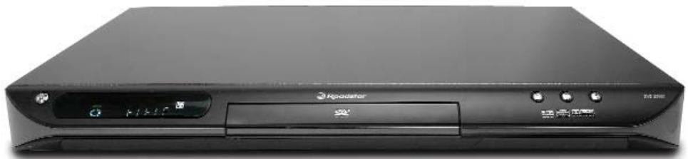
Superslim PAL/NTSC Home DivX player, DVD / MPEG4 / SVCD / Audio CD / MP3 / WMA and Picture CD (JPEG) compatible, down-mixed two channel Stereo Audio Output, S-Video + SCART Output, Audio Digital & Progressive Scan output.
DEUTSCH
- Upgradable firmware (via CD-R)
DivX 6.0 Compatible - NTSC and PAL video signals playback
- Down Mixed audio output
8 languages
On Screen Display
- Slow motion / Fast forward
- Support up to 8 audio lang.
- Support up to 32 subtitles languages
- Program function
- Repeat / random play mode
- Selectable screen ratio
(4:3 and 16:9) - Multi-angle function
- Zooming function
- Parental control
- MP3 disc playback with detailed OSD info
- Progressive scan output (480p and 720p supported)
Input / Output
2 channel Audio output (RCA)
S-Video output
- SCART connector
Composite video output
- Component video output (Pb, Pr, Y)
Coaxial & Optical digital audio output
Ean code: 76 21800 02532 6
General
Full function remote control
- Scart cable
-
Dimensions (WxHxD):
430 × 52 × 270 mm
Weight: 2.9kg
Colour: Mirror / Silver -
Container load:
40' 3'296 pcs
20' 1'580 pcs
- Shipping carton: 4 pcs
- Shipping cart. size (WxHxD): 390 x 342 x 530 mm
- Gift Box size (WxHxD):
520 × 335 × 93 mm
Country of origin: P.R.C.
CONTENTS :
1.INFORMATIONS. 3 Vibratto-II DVD Processor (ESS 66x8)
2. OPERATING INSTRUCTIONS 14
3.PRODUCT SPECIFICATIONS. 24
4. TROUBLESHOOTING 25
5. MAINTENANCE INSTRUCTIONS 26
6. ELECTRICAL PART LIST 35
7. DISASSEMBLY AND REASSEMBLY 43
8.CIRCUIT DIAGRAMS 44
9. WIRING DIAGRAM 49
1.INFORMATIONS
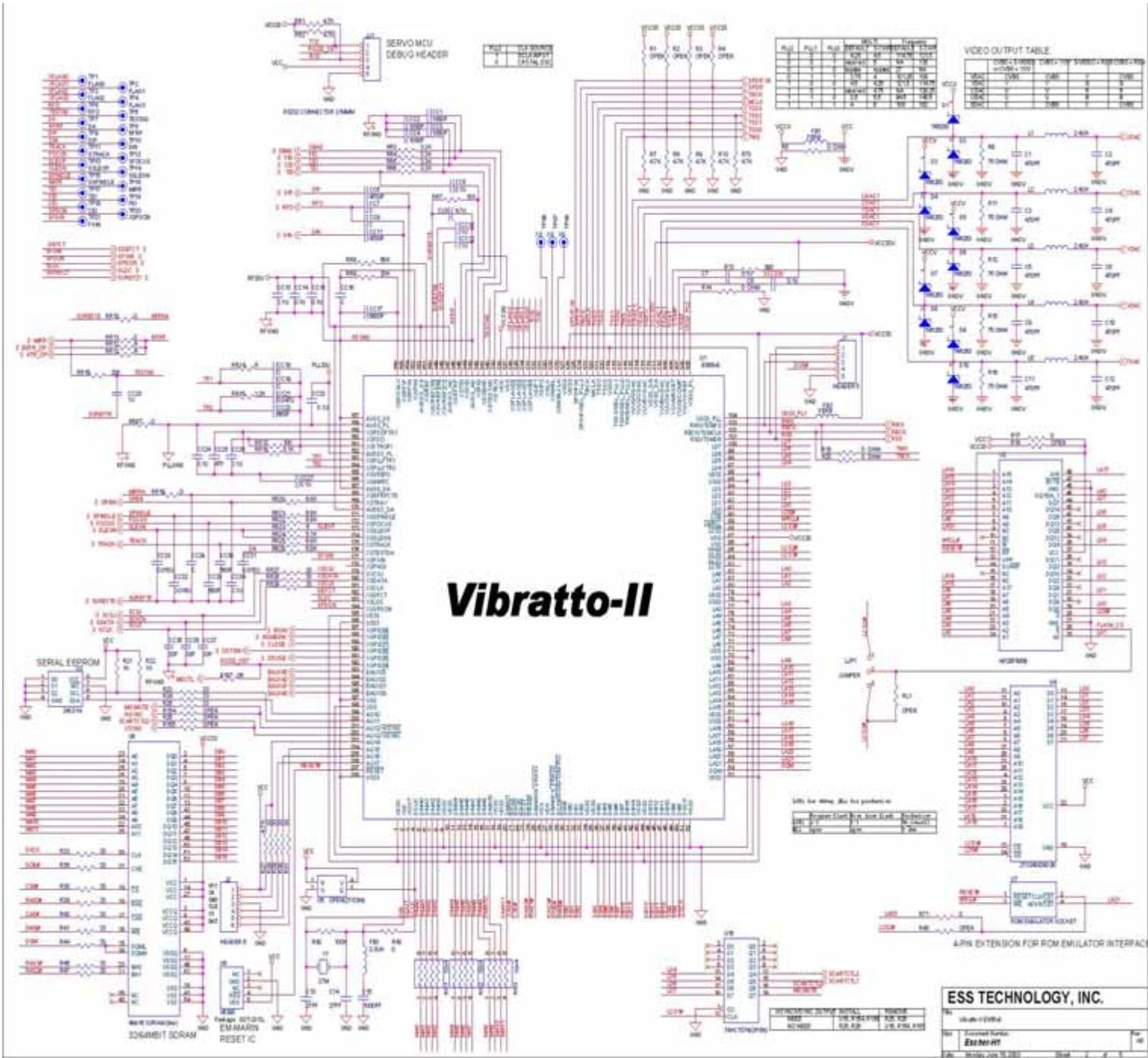
Vibratto-II DVD Processor (ESS 66x8)
Vibratto-II DVD Processor
FEATURES:
- Single-chip DVD processoe incorporating all front-end and back-end functions
- Unified memory architecture
- Proven focusing, sledding, tracking, and CLV/CAV spindke servo control
Proven ESS, EFM,?EFM+ demodulation, and EDC circuit
Built-in ADCs and DACs for servo control signals - Direct interface to ES6603 servo AFE chip
- Integrated NTSC/PAL encode with pixel-adaptive de-interlacer and five 10-bit 54MHz video DACs
DVD-video, DVD-VR, VCD1.1 and 2.0, and SVCD
DivX and MPEG-4 Advanced Simple profile at full screen(D1) - Full DVD-audio support including MLP and LPCM decode, CPPM decryption, and watermark detection
- Media playback with CD-ROM, CD-R/RW, DVD-R/RW, and DVD+R/RW
Up to 7.1 channel audio outputs - Direct interface of 16 bit DRAM up to 128Mb capacity
- Direct interface for up to 4 banks of 8-bit EPROM or FLASH EPROM for up to 4MB per bank
- Macrovision 7.1 for NTSC/PAL (480p/576p) progressie scan video
- Simultaneous composite,S-video and YUV output
CCIR656/601 yuv 4:2:2 output - OSD controller supports 256 colors in 8 degrees of transparency
- Subpicture Unit(SPU) decoder supports karaoke iyric, subtitles, and EIA-608 compliant Line 21 Captioning.
- SmartBright™ for clear and bright movie presentation.
- SmartColor™ for vivid flesh-tone image display.
- SmartLogo™ for custom JPEG wallpaper.
JPEG digital photo CD support (Kodak Picture CDTM and Fujifilm FujiColor CDTM .
ESS Music SlideshORTM. - Bass management.
- Dolby Digital(AC-3), Dolby ProLogic™, and ProLogicII.
- DTS™ surround(ES6698D only).
S/PDIF digital audio input and output. - MPEG AAC and Multichannel.
SRS TruSurround
Professional karaoke with full scoring scheme.
Functional Description:
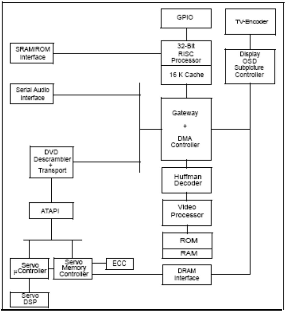
The internal block digram for ESS 6698
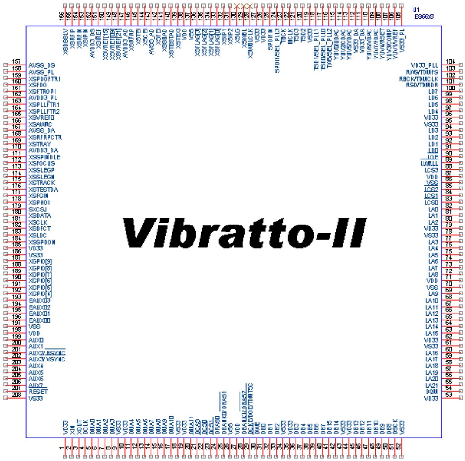
Pinout Diagram
| Names | Pin Numbers | I/P | Definitions | ||||
| VD33 | 1.10.19.35.44.53.62.79.96.126.185. | P | I/O power supply. | ||||
| VID_XI | 2 | I | Crystal input. | ||||
| VID_XO | 3 | O | Crystal output. | ||||
| VID_XO | 3 | O | Crystal output. | ||||
| CLK | 4 | I | System clock. | ||||
| DMA[11:0] | 5:8 11:17 20 | O | DRAM address bus. | ||||
| VX33 | 9.18.34.43.52.61.78.95.119.127.186.208 | G | Ground for I/O power supply. | ||||
| DCAS# | 21 | O | DRAM column address strobe (active-low). | ||||
| DCS[1:0]# | 22.23 | O | DRAM chip select (active-low). | ||||
| DRAS[2:0]# | 24.25.28 | O | DRAM row address strobe (active-low). | ||||
| VSS | 26.70.86.137.197 | G | Ground for core power supply. | ||||
| VDD | 27.71.87.138.198 | P | Core power supply. | ||||
| DSCK_EN | 29 | O | DRAM clock enable output . | ||||
| DOE# | O | DRAM output enable(active-low). | |||||
| DWE# | 30 | O | DRAM write enable(active-low). | ||||
| DB[15:0] | 31:33,36:42,45:50 | I/O | DRAM data bus. | ||||
| DSCK | 51 | O | Output clock to DRAM. | ||||
| DQM | 54 | O | Data input/output mask. | ||||
| LA[21:0] | 55:60,63:69,72:7780:82 | O | RISC port address bus . | ||||
| LCS[3:0]# | 83:85 88 | O | RISC port chip select (active-low). | ||||
| LWRLL# | 89 | O | RISC port low-byte write enable(active-low). | ||||
| LOE# | 90 | O | RISC port output enable (active-low). | ||||
| LD[7:0] | 91:94,97:100 | I/O | RISC port data bus; (5V tolerant input). | ||||
| RSD | 101 | I | Audio receive serial data; (5V tolerant input ). | ||||
| RBCK | 102 | I | Audio receive bit clock; (5V tolerant input ). | ||||
| RWS | 103 | I | Audio receive frame sync; (5V tolerant input ). | ||||
| VD33_PL | 104 | P | Power for PLL blocks. | ||||
| VS33_PL | 105 | G | Ground for PLL blocks. | ||||
| VREF | 106 | I | Internal voltage reference to video DAC. | ||||
| YUV1 | O | YUV pixel 1 output data . | |||||
| COMP | 107 | I | Compensation input . | ||||
| YUV3 | O | YUV pixel 3 output data . | |||||
| RSET | 108 | I | DAC current adjustment resistor input . | ||||
| YUV4 | O | YUV pixel 4 output data. | |||||
| FDAC | 109 | O | Video DAC output. Refer to description and matrix forUDAC pin 115. | ||||
| YUV7 | O | YUV pixel 7 output data . | |||||
| VDAC | 110 | O | Video DAC output . Refer to description and matrix for UDAC pin 115. | ||||
| YUV6 | O | YUV pixel 6 output data . | |||||
| Names | Pin Numbers | I/P | Definitions | ||||
| VD33_DA | 111 | P | Power for I/O power supply for VDAC. | ||||
| VS33-DA | 112 | G | Ground for I/O power supply for VDAC. | ||||
| YDAC | 113 | O | Video DAC output. Refer to description and matrix for UDAC pin 115. | ||||
| YUV5 | O | YUV pixel 5 output data . | |||||
| CDAC | 114 | O | Video DAC output. Refer to description and matrix for UDAC pin 115. | ||||
| YUV2 | O | YUV pixel 2 output data . | |||||
| UDAC | O | Video DAC output. | |||||
| Pin | 109 | 110 | 113 | 114 | |||
| Valu e | FDAC | VDAC | YDAC | CDAC | |||
| 0 | CVBS/Chrom a | CVBS 1 | Y | C | |||
| 1 | CVBS/Chrom a | CVBS 1 | Y | C | |||
| 2 | CVBS/Chrom a | N/A | Y | C | |||
| 3 | CVBS/Chrom a | CVBS 1 | N/A | N/A | |||
| 4 | CVBS/Chrom a | CVBS 1 | N/A | N/A | |||
| 5 | CVBS/Chrom a | CVBS 1 | Y | Pb | |||
| 6 | CVBS/Chrom a | N/A | Y | Pb | |||
| 7 | N/A | SYNC | G | B | |||
| 8 | CVBS/Chrom a | Chrom a | Y | Pb | |||
| 9 | CVBS | CVBS 1 | G | B | |||
| 10 | CVBS | CVBS 1 | G | R | |||
| 11 | N/A | SYNC | G | R | |||
| 12 | CVBS/Chrom a | N/A | Y | Pr | |||
| 13 | CVBS/Chrom a | CVBS 1 | Y | Pr | |||
| 14 | Chroma | Y | G | R | |||
| F:VCBS/chroma signal for simultaneous mode. Y:Luma component for YUV and Y/C processing. | |||||||
| C: Chrominance signal for Y/C processing. U: Chrominance component signal for YUV mode. V: Chrominance component signal for YUV mode. | ||||||
| TWS | 116 | O | Audio transmit frame sync output. | |||
| Names | Pin Numbers | I/P | Definitions | |||
| SEL_PLL2 | I | System and DSCK output clock frequency selection is made at the rising edge of RESET#. The matrix below lists the available clock frequencies and their respective PLL bit settings. Strapped to VCC or ground via 4.7-KΩ resistor; read only during reset. | ||||
| SEL_PLL2 | SEL_PLL1 | SEL_PLL0 | Clock Type(MHz) | |||
| 0 | 0 | 0 | CLK*4.5 | |||
| 0 | 0 | 1 | CLK*5.0 | |||
| 0 | 1 | 0 | Bypass | |||
| 0 | 1 | 1 | CLK*4.0 | |||
| 1 | 0 | 0 | CLK*4.25 | |||
| 1 | 0 | 1 | CLK*4.75 | |||
| 1 | 1 | 0 | CLK*5.5 | |||
| 1 | 1 | 1 | CLK*6.0 | |||
| TSD0 | 117 | O | Audio transmit serial data port 0. | |||
| SEL_PLL0 | I | Refer to the description and matrix for SEL_PLL2 pin 116. | ||||
| TSD1 | 118 | O | Audio transmit serial data port 1. | |||
| SEL_PLL1 | I | Refer to the description and matrix for SEL_PLL2 pin 116. | ||||
| TSD[2:3] | 120.121 | O | Audio transmit serial data ports 2 and 3. | |||
| MCLK | 122 | I/O | Audio master clock for audio DAC. | |||
| TBCK | 123 | O | Audio transmit bit clock. | |||
| SPD_DOBM | 124 | O | S/PDIF output . | |||
| SEL_PLL3 | I | Clock source select. Strapped to VCC or ground via 4.7K Ω read only during reset . | ||||
| SEL_PLL3 | Clock Source | |||||
| 0 | Crystal oscillator | |||||
| 1 | CLK input | |||||
| SPDIF_IN | 125 | I | S/PDIF input; (5V tolerant input). | |||
| WBLCLK | 128 | O | DVD-RAM wobble detector circuit clock source to preamp. | |||
| WBL | 129 | O | DVD-RAM wobble output. | |||
| LG | 130 | O | DVD-RAM land/groove flag. | |||
| IP2 | 131 | I | DVD-RAM header position index 2. | |||
| IP1 | 132 | I | DVD-RAM header position index 1. | |||
| FLAG[3:0] | 133:136 | O | To monitor servo status . | |||
| TEXI | 139 | I | High-speed tracking error input . | |||
| TESTAD | 140 | I | Test AD input . | |||
| SBAD | 141 | I | Sub-beam addition input signal . | |||
| FEI | 142 | I | Focus input error signal. | |||
| AVSS_AD | 143 | G | Analog ground for ADC block . | |||
| CEI | 144 | I | Center error input signal. | |||
| TEI | 145 | I | Tracking error input signal. | |||
| RFRP | 146 | I | RF ripple/envelope input signal. | |||
| AVDD3_AD | 147 | P | Analog power supply for ADC block. | |||
| VREF21 | 148 | O | 2.1V reference voltage. | |||
| VREF09 | 149 | O | 0.9Vreference voltage. | |||
| VREF15 | 150 | O | 1.5V reference voltage. | |||
| Names | Pin Numbers | I/P | Definitions | |||
| IREF | 151 | I | Servo data PLL interface reference current generator connect a resistor between this pin and ground to set reference current. | |||
| AVDD3_DS | 152 | P | Analog power supply for data slicer .block. | |||
| IPIN | 153 | I | Inverting input of data slicer . | |||
| RFIN | 154 | I | Analog RF signal input after passing through equalizer(minus) | |||
| RFIP | 155 | I | Analog RF signal input after passing through equalizer(plus). | |||
| DSSLV | 156 | O | Data slicer level output. | |||
| AVSS_DS | 157 | G | Analog ground for data slicer block. | |||
| AVSS_PL | 158 | G | Analog ground for data PLL block. | |||
| PDOFTR1 | 159 | O | Servo data PLL phase detector filter pin number 1. | |||
| FDO | 160 | O | Servo data PLL output node of frequency detector charge pump. | |||
| FTROPI | 161 | I | Servo data PLL input node of loop filter OP circuit. | |||
| AVDD3_OL | 162 | P | Analog power supply for data PLL block. | |||
| PLLFTR1 | 163 | I | Servo data PLL loop filter pin number1. | |||
| PLLFTR2 | 164 | I | Servo data PLL loop filter pin number2. | |||
| VREF0 | 165 | O | Servo data PLL reference voltage output. | |||
| AWRC | 166 | I/O | Auto wide range control VCO signal from/to AWRC DAC. | |||
| AVSS_DA | 167 | G | Analog ground for DAC part. | |||
| RFRPCTR | 168 | I/O | Central level of RFRP. | |||
| TRAY | 169 | O | Output voltage level for tray buffer IC. | |||
| AVDD3_DA | 170 | P | Analog power supply for DAC part. | |||
| SPINDLE | 171 | O | Output voltage level for spindle buffer IC. | |||
| FOCUS | 172 | O | Output voltage level for focus buffer IC. | |||
| SLEGP | 173 | O | Output voltage level for Sledge buffer IC(zplus). | |||
| SLEGN | 174 | O | Output voltage level for Sledge buffer IC(minus). | |||
| TRACK | 175 | O | Output voltage level for tracking buffer IC. | |||
| TESTDA | 176 | O | Test DA output. | |||
| FGIN | 177 | I | Spindle hall sensor input. | |||
| PHOI | 178 | I | Sledge photo interrupt signal input. | |||
| SCSJ | 179 | O | Chip selection signal to RF chip (serial data enable). | |||
| SDATA | 180 | I/O | Data signal from/to RF chip. | |||
| SCLK | 181 | O | Serial clock source to RF chip. | |||
| DFCT | 182 | I | Defect flag input signal. | |||
| LDC | 183 | O | Laser diode on/off control output. | |||
| SPDON | 184 | O | Spindle power driver on/off control output. | |||
| GPIO[9:4] | 187:192 | I/O | General-purpose input/output used for servo control; (5V tolerant input.) | |||
| EAUX[3:0] | 193:196 | I/O | Extended auxiliary ports;(5V tolerant input). | |||
| I²CDATA | 199 | I/O | I²C data I/O;(5V tolerant input). | |||
| AUX0 | I/O | Auxiliary port (open collector);(5V tolerant input). | ||||
| I²C_CLK | 200 | I/O | I²C clock I/O;(5V tolerant input). | |||
| AUX1 | I/O | Auxiliary port (open collector);(5V tolerant input). | ||||
| IOW# | 201 | O | I/O Write strobe(LCS1)(active-low). | |||
| HSYNC# | I/O | Horizontal sync (active low);(5V tolerant input). | ||||
| AUX2 | I/O | Auxiliary port; (5V tolerant input). | ||||
| Names | Pin Numbers | I/P | Definitions | |||
| IOR# | 202 | O | I/O Read strobe (LCS1)(active -low). | |||
| VSYNC# | I/O | Vertical sync (active-low);(5V tolerant input ). | ||||
| AUX3 | I/O | Auxiliary port; (5V tolerant input). | ||||
| C2PO | 203 | I | Error correction flag from CD;(5V tolerant input). | |||
| AUX4 | I/O | Auxiliary port; (5V tolerant input). | ||||
| AUX[5:6] | 204:205 | I/O | Auxiliary ports ;(5V tolerant input). | |||
| IR | 206 | I | Infrared remote control input;(5V tolerant input). | |||
| AUX7 | I/O | Auxiliary port; (5V tolerant input ). | ||||
| RESET# | 207 | I | Reset input (active -low);(5V tolerant input). | |||
| Audio Port Interface | 101 | I | Audio receive serial data input[RSD];(5V tolerant input). | |||
| 102 | I | Audio receive bit clock input [RBCK];(5V tolerant input ). | ||||
| 103 | I | Audio receive frame sync input[RWS];(5V tolerant input). | ||||
| 116 | O | Audio transmit frame sync output[TWS]. | ||||
| 117.118.120.121 | O | Audio transmit serial data outputs [TSD[3:0]]. | ||||
| 122 | I/O | Audio DAC master clock[MCLK]. | ||||
| 123 | O | Audio transmit bit clock output[TBCK]. | ||||
| 124 | O | Sony/Philips Digital Interface audio output [SPD_DOBM]. | ||||
| 125 | I | Sony/Philips Digital Interface audio Input [SPDIF_IN];(5V tolerant input). | ||||
| Auxiliary Port Interface | 193:196 | I/O | Extended auxiliary ports [EAUX[3:0]];(5V tolerant input). | |||
| 199.200 | I/O | Open collectors [AUX[1:0] ,(5V tolerant input). | ||||
| 201:206 | I/O | Primary auxiliary port I/Os [AUX[7:2] ;(5V tolerant input). | ||||
| Clock Inface and Reset | 2 | I | 27-MHz crystal clock input [VID_XI]. | |||
| 3 | O | 27-MHz crystal clock output[VID_XO]. | ||||
| 4 | I | System clock [CLK]. | ||||
| 29 | O | DRAM clock enable output [DSCK_EN]. | ||||
| 51 | O | Output clock [DSCK] to video memory (DRAM). | ||||
| 116:118 | I | Clock frequency select PLL outputs [SEL_PLL[2:0]]. | ||||
| 207 | I | Reset input (active-low)[RESET#];(5V tolerant input). | ||||
| Display Interface | 106:110.113:115 | O | Pixel data outputs [YUV[7:0]]. | |||
| 201 | I/O | Horizontal sync[HSYNC#];(%V tolerant input). | ||||
| 202 | I/O | Vertical sync [VSYNC#];(5V tolerant input). | ||||
| EPROM/Flas h ROM and RISC Port Inteface | 55:60.63:69.72:77.80:82 | O | RISC port address bus [LA[21:0]]to EPROM or Flash memory. | |||
| 83:85 | O | RISC port chip select outputs [LCS[2:0]#]to EPROM or Flash memory. | ||||
| 89 | O | RISC port low-byte write enable output[LWRLL#]to EPROM or Flash memory. | ||||
| 90 | O | RISC port output enable[LOE#]to EPROM and Flash memory. | ||||
| 91:94.97:100 | I/O | RISC port data bus [LD[7:0]]to EPROM or Flash memory (5V tolerant input). | ||||
| Filter and Reference voltang Interface | 106 | I | Video DAC reference voltage input[VREF]. | |||
| 107 | I | Compensation input[COMP]. | ||||
| Front Panel Display Interface | 206 | I | Infrared remote control input [IR];(5V tolerant input). | |||
| Names | Pin Numbers | I/P | Definitions | |||
| General-Purp ose | 187:192 | I/O | General -purpose I/O[GPIO[9:4]];(5V tolerant input). | |||
| I²C Bus Interface | 199 | I/O | I²C data I/O[12C_DATA];(5V tolerant input). | |||
| 200 | I/O | I²C clock I/O[12C_CLK];(5V tolerant input). | ||||
| Power and Ground | 1.10.19.35.44.53.62.79.96.126.185 | P | I/O power supply [VD33]. | |||
| 9.18.34.43.52.61.78.95.119.127.186.208 | G | I/O ground [VS33]. | ||||
| 26.70.86.137.197 | G | Ground for core power [VSS]. | ||||
| 27.71.87.138.198 | P | Core power supply [VDD]. | ||||
| 104 | P | Power supply for PLL block .[VD33_PL]. | ||||
| 105 | G | Ground for PLL block [VS33_PL]. | ||||
| 111 | P | Power supply for video DAC[VD33_DA]. | ||||
| 112 | G | Ground for video DAC[VS33_DA]. | ||||
| 143 | G | Analog ground for ADC[AVSS_AD]. | ||||
| 147 | P | Analog power supply for ADC[AVDD3_AD]. | ||||
| 152 | P | Analog power supply for data slicer [AVDD3_DS]. | ||||
| 157 | G | Analog ground for data slicer[AVSS_DS]. | ||||
| 158 | G | Analog ground for data PLL [AVSS_PL]. | ||||
| 162 | P | Analog power supply for data PLL[AVDD3_PL]. | ||||
| 167 | G | Analog ground for DAC[AVSS_DA]. | ||||
| 170 | P | Analog power supply for DAC[AVDD3_DA]. | ||||
| Serial Port Interface | 203 | I | C2PO error correction flag from CD[C2PO];(5V tolerant input). | |||
| Servo Data Slicer Interface | 153 | I | Inverting input of data slicer [IPIN]. | |||
| 154 | I | Analog RF signal input after passing through equalizer(minus) [RFIN]. | ||||
| 155 | I | Analog RF signal input after passing through equalizer(plus) [RFIP]. | ||||
| 156 | O | Data slicer level output[DSSLV]. | ||||
2.OPERATING INSTRUCTIONS
1. GENERAL SETUP
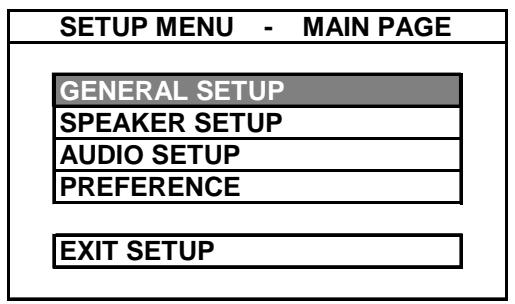
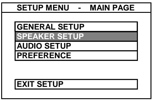
Pressing the SETUP button on remote control during STOP or PLAY mode to SETUP MENU.
Cursor to select GENERAL SETUP. Press ENTER to enter GENERAL SETUP page.

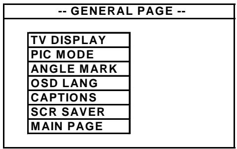
a.TV DISPLAY
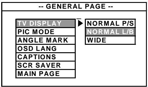
Using cursor to move to desired setting and press ENTER to confirm.
NORMAL/PS - 4 x 3 Pan Scan
Full screen of picture on TV. Normally, left and right edges cannot be shown.
NORMAL/LB - 4 x 3 Letter Box
Original ratio of aspect.
WIDE - 16 : 9 Widescreen
b. PIC MODE (PICTURE MODE)
(FOR PROGRESSIVE-SCAN MODEL)
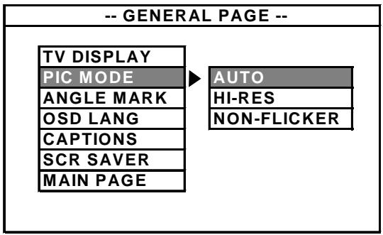
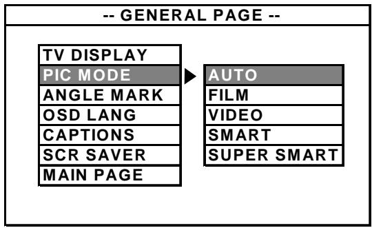
c.ANGLE MARK
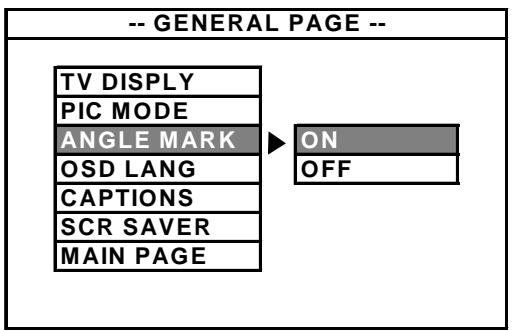
This feature is functioned only for the disc, which has ANGLE function:
When the ANGLE MARK is set ON, the screen displays the mark.
When the ANGLE MARK is set OFF, the mark is not displayed.
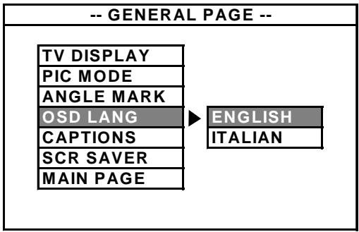
d. OSD LANG (ON SCREEN DISPLAY LANGUAGE)
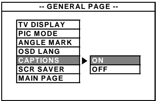
e. CAPTIONS
f. SCR SAVER
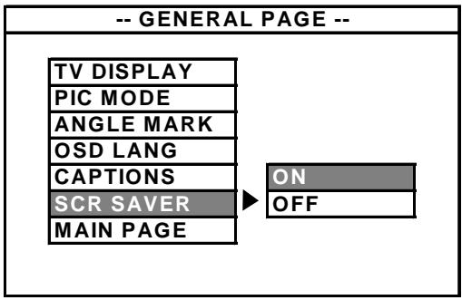
When the unit is stopped, no operation, no function button is pressed in 1 minute, screen saver appears for the purpose to protect the TV screen if SCR Saver is set ON.
2.SPEAKER SETUP
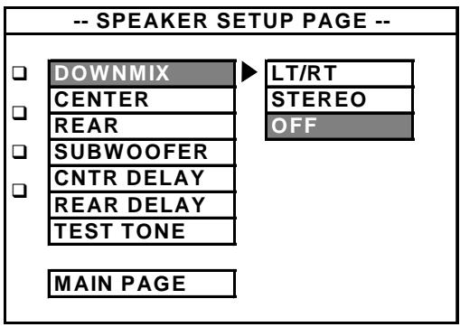
a. DOWNMIX
b. CENTER
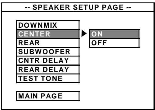
d. SUBWOOFER
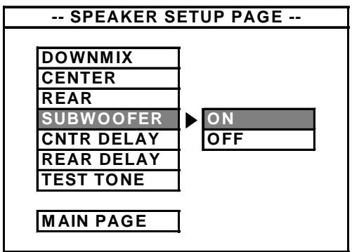
LT/RT : Left and Right output mode
STEREO: Stereo output mode
OFF: Turn off the Downmix mode. 5.1 channels can be preformed only if
Downmix is set OFF and the rest of other setup can be activated.
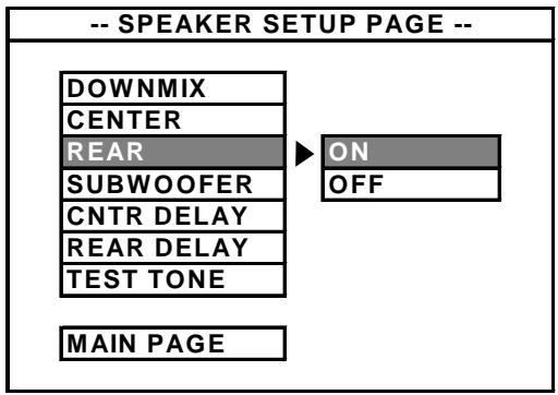
c. REAR
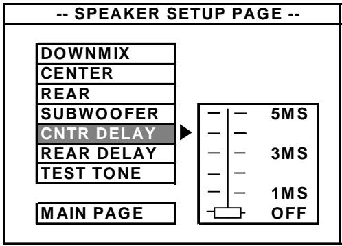
e. CNTR DELAY
Adjust the audio delay from center
channel from 0 to 5MS.
f. REAR DELAY
Adjust the audio delay from center
channel rom 0 to 15MS.
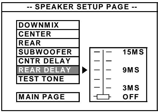
g. TEST TONE
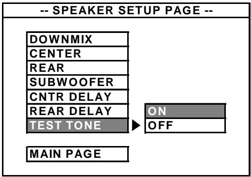
ON: open the 5.1 channel test function.
OFF: turn off the 5.1 channel test function.
3.AUDIO SETUP
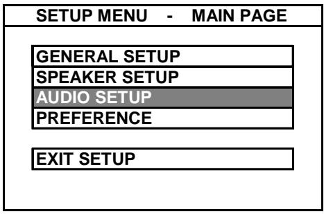
a. SPDIF OUTPUT
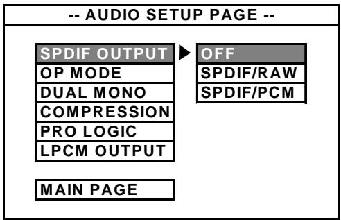
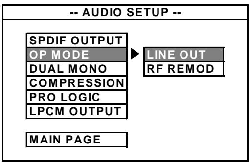
b. OP MODE
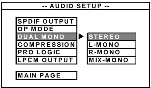
c. DUAL MONO
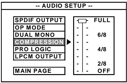
d.COMPRESSION
OFF: Audio signal is out from AUDIO OUT (RCA) jacks.
SPDIF/RAW: The player is connected to a Dolby Digital amplifier through DIGITAL OUT Coaxial or Optical jack.
SPDIF/PCM: The player is connected to a 2-channel digital mode or stereo amplifier through Coaxial or Optical jack.
LINE OUT: Line out mode with digital dialog normalization, compress input linear signal.
RF REMOD : RF remodulation mode with heavy compression and digital dialog normalization.
Output mode of the L/R signals. Mix-mono can be functioned only if the DVD is playing in 5.1 channel.
To adjust linear compression rate to obtain the different compression results of the signals only if the OP MODE is set to LINE OUT.
The default setting of password is 3308
To select an age control grade according to the grade of the disc and your desired. The disc cannot be played for the rate higher than the grade set.
Go to the PASSWORD VERIFY PAGE to input password after selection of Parental grade.
i. DEFLAUTS
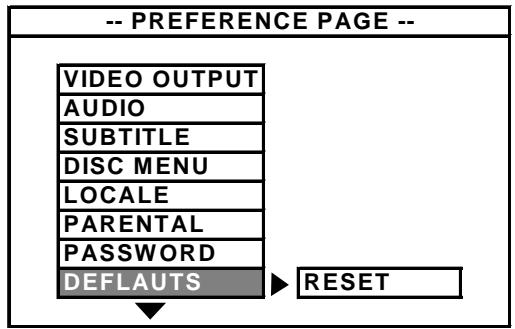
To reset the settings to factory setting
j. SMART NAVI
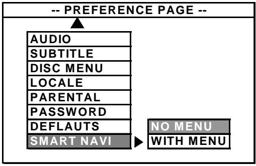
To select the display with MENU for playing MP3 and PHOTO CD (JPEG).
5. JPEG, MP3 & MPEG4 Format
(Playback of MP3, WMA, CD-R and CD-RW may depend on recording condition)
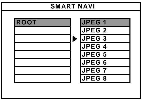
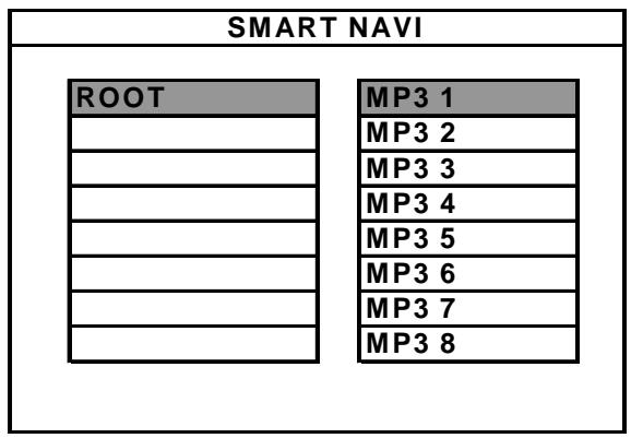
Press to select the „ROOT“ on the left columns & the „FILE“ on the right side, press ENTER“/”“PLAY“ to view the JPEG PHOTOS or to play MP3 files. Then press “STOP” to go back to the menu of SMART NAVI”.
FUNCTION KEYS
Zoom Press the “ZOOM” Button, then the screen will show “ZOOM ON”, and press Icons to “zoom in” or “zoom out”.
Rotate Press to rotate the picture
Next/ Press to the next or previous pictures/songs.
Previous
Forward/ Press the icons to playing fast forward ans fast backward. Backward
Menu Press "Menu" to preview the photos.
Mute Press "MUTE" button to turn the audio off. Press it again to resume.
Pause Press to pause playin & press again to resume.
MPEG4 FORMAT
| SMART NAVI | |
| ROOT | MP4 1 |
| MP4 3 | |
| MP4 3 | |
| MP4 4 | |
| MP4 5 | |
| MP4 6 | |
| MP4 7 | |
| MP4 8 | |
FUNCTION KEYS
Forward/ Press the icons to playing fast forward and fast backward. Backward Continuously pressing and back to normal.
Next/ Press to the next or previous chapter or files. Previous
Mute Press "MUTE" button to turn the audio off. Press it again to resume.
Pause Press to pause playing & press again to resume.
Slow Press "SLOW" and playback of slow motion. Please "Play" to resume it.
Step Keeping press "STEP" repeatedly button to playing frames by frames.
GoTo Search the chapter and time you want. Functions please refer to "Function Buttons" on instruction book.
Subtitle In order to use the function of Subtitle (For the MPEG4 file with subtitle function): Insert disc and choose the file in “?” icon, then press ‘ANGLE’ button in remote control, the screen will shown subtitle is being selected. Then get back to the appropriate .avi file and press ‘ENTER’ to playback, then the subtitle function is activate.
3.PRODUCT SPECIFICATIONS
A. Playback System
| DVD Video |
| Video CD (1.1, 2.0, 3.0) |
| SVCD |
| CD and CDDA |
| CD-R/RW |
| PICTURE CD |
B. Television Signal System
NTSC/PAL
C. Video Performance
| Video Out | 1Vppinto 75ohm |
| S-Video Out | Y: 1Vppinto 75ohm C: 0.286Vppinto 75ohm |
| D/A Converter | 27MHz/10 bit |
D. Audio Performance
| Frequency Response | DVD: fs48//96KHz, 4Hz-22/44KHz Video CD: fs 44.1KHz, 4Hz-20KHz Audio CD: fs44.1KHZ, 4Hz-20KHz |
| Output Level | Analog: 2VRMS(1KHZ) Digital: 1.15VPP |
| D/A Converter | 96KHz/24bit |
| S/N Ratio | With LPF 95dB Without LPF 90dB |
E. Connections
| Coxial digital out | X1 |
| Digital out | X1 |
| Audio Analog out (5.1ch) | X1 |
| S-Video out | X1 |
F. Power Supply
| Power Source | AC 90-250V 50/60Hz |
| Power Consumption | <25 Watt |
4.TROUBLESHOOTING
| Symptom | Check and Action |
| No Power | 1. Check the power cord has been properly connected to the wall outlet 2. Check the main power has been switched on |
| Do not play | 1. No disc, load a disc 2. Disc has been loaded upside down. Place the disc with the label side up 3. Disc's region code is not matching to the unit 4. Disc is not correct type to be played 5. Disc is damaged or dirty, clean the disc or try another disc 6. Moisture may be condensed inside the unit. Remove the disc and leave the unit power on for one or two hours |
| No Picture | 1. Check the TV set has been power on, and setting at the correct AV mode 2. Check the system connection is secure 3. Check if the connection cables are damaged 4. Clean the disc |
| Picture noise / distorted | 1. Disc is dirty or damaged. Clean the disc or try another disc 2. Reset the color system of the DVD unit or the TV set 3. Try to direct the DVD unit to the TV set instead of via the components like VCR. |
| Picture not full screen | 1. Select the screen format. Enter SETUP MENU → (TV DISPLAY) 2. Select the screen format from DVD disc menu |
| Cannot SKIP or SEARCH | 1. Some disc are programmed that do not allow users to SKIP or SEARCH forward at some sections, especially at the beginning WARNING section 2. Single Chapter disc cannot apply SKIP function |
| No sound or Sound output not complete | 1. Check the TV and amplifier has been power on and correctly setting 2. Check the TV and amplifier system connections are secure 3. Press AUDIO button select other audio tracks output of disc 4. Check if the MUTE function of the DVD, TV or amplifier has been activated 5. There will be no sound output during REVERSE PLAY / PAUSE / STEP / SLOW / SEARCH |
5.MAINTENACF INSTRUCTIONS
INDEX
a. No power
Please see Figure 1
b. No LED display
Please see Figure2
c. No video output
Please see Figure3
d. cannot read disc
Please see Figure4
e. Remote control no function
Please see Figure6
f. No 2ch output
Please see Figure7
g. Disc door cannot open
Please see Figure8
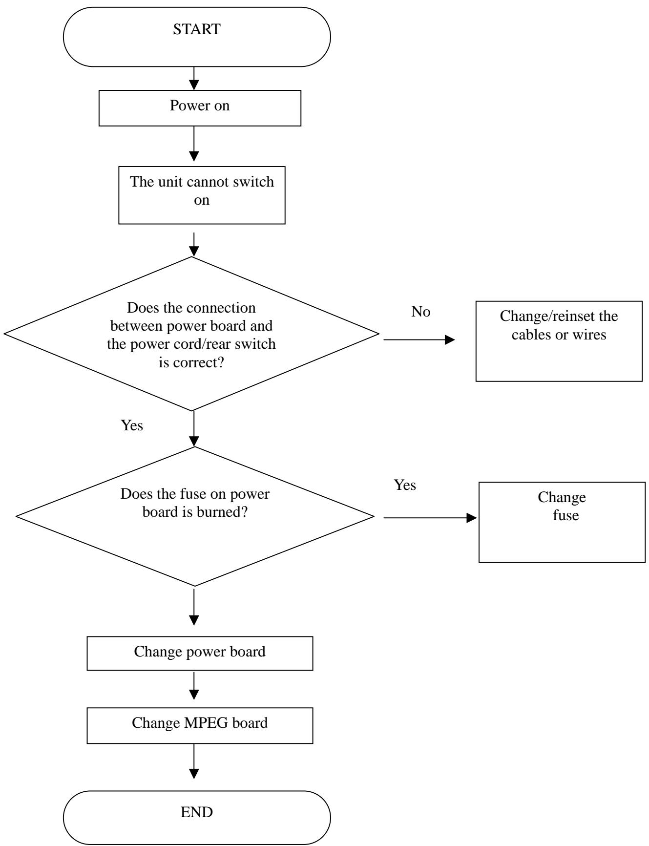
(i) Figure 1
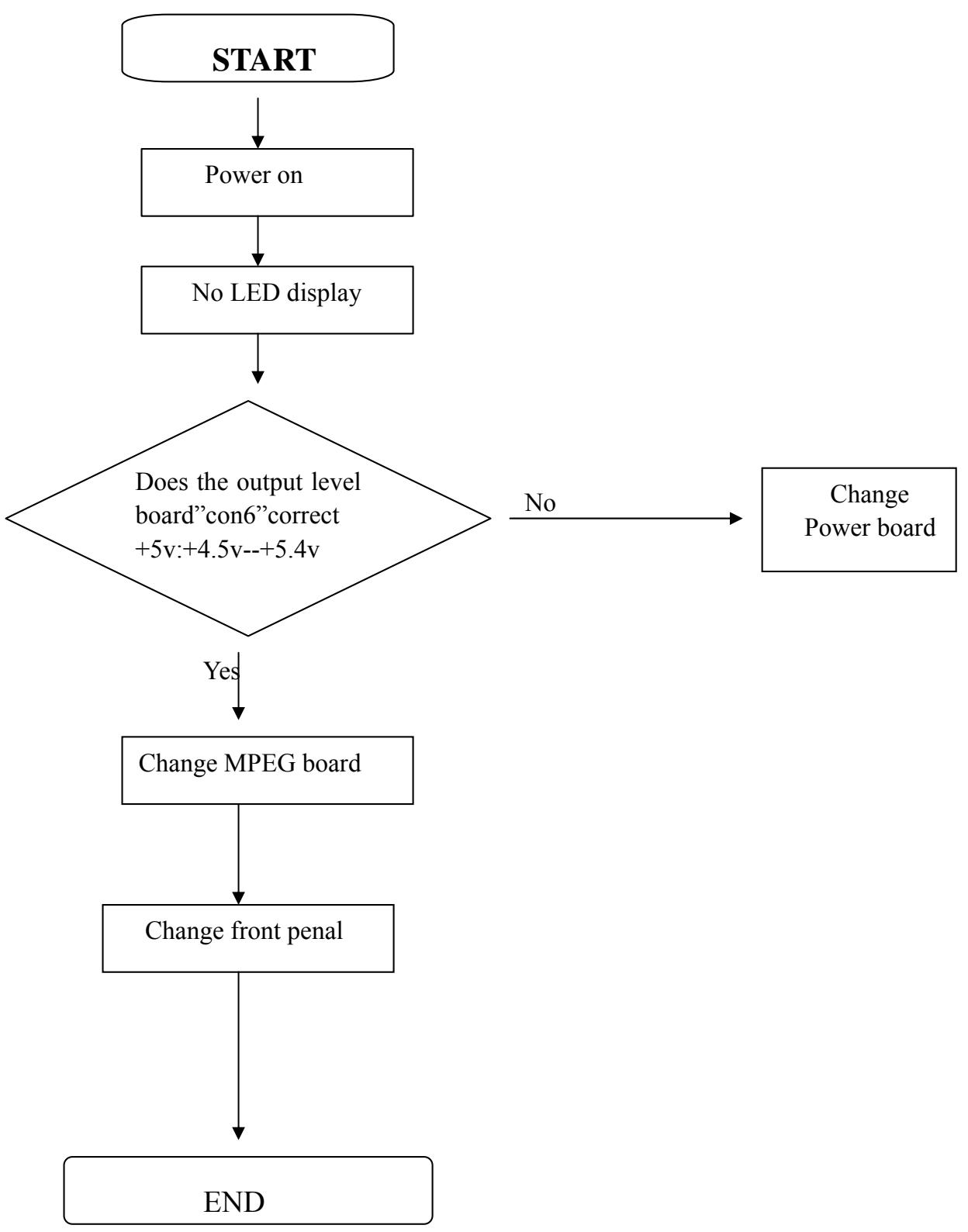
(ii)Figure2
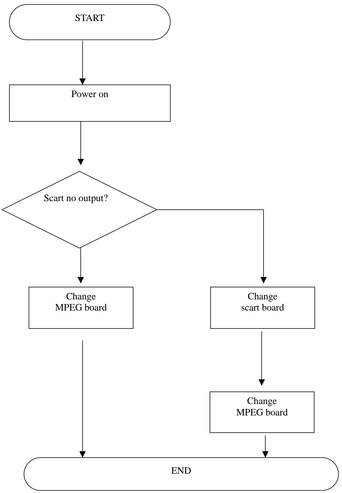
(iii)Figure 3
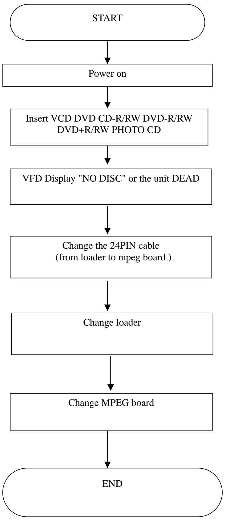
(iv)Figure 4
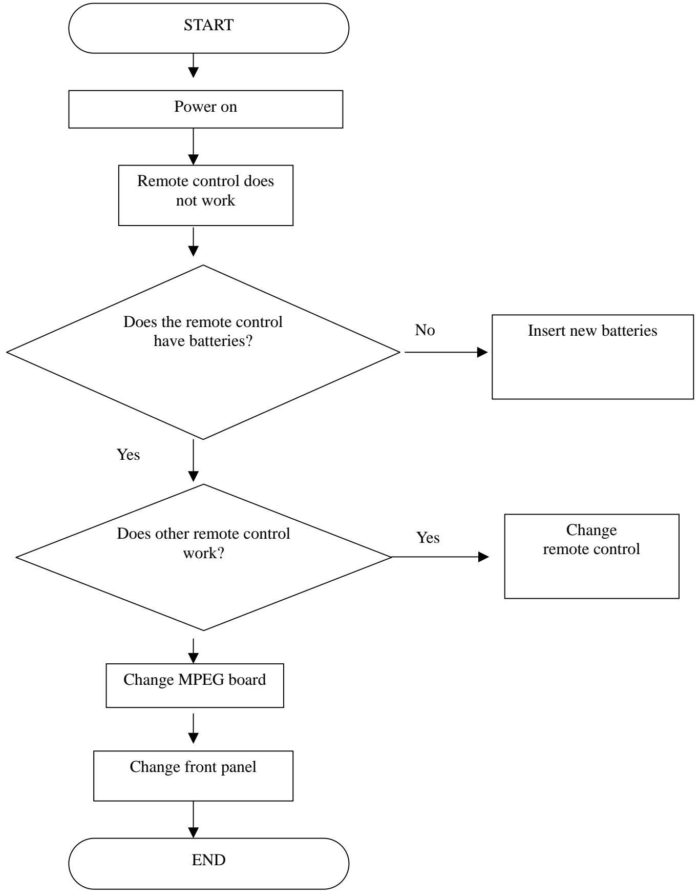
(vi) Figure 6
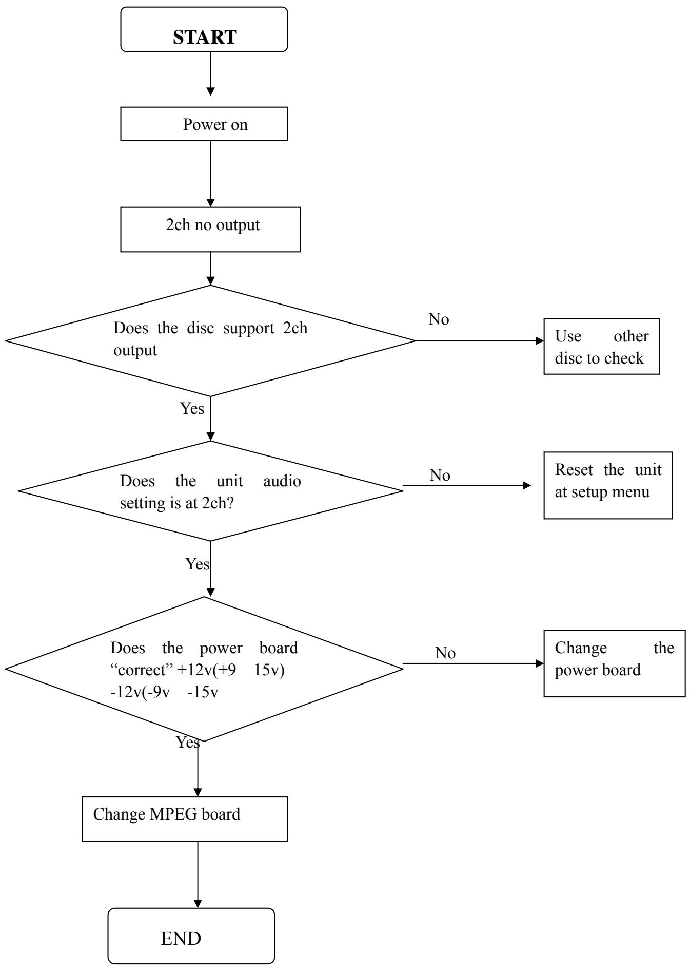
(vii)Fiure7
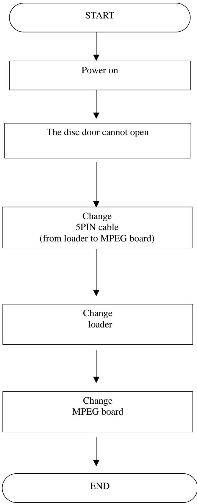
(viii)Figure 8
6.ELECTRICAL PART LIST
A. MPEG board
| Item | Name of Components | Specification | Qty | Location |
| 1 | Pcb | ESS-66X8PCBREV:1.5 | 1 | |
| 2 | IC | 8MFLASH 29F800BA-70PFTN | 1 | U2 |
| 3 | IC | ES6698 | U1 | |
| 4 | IC | SDRAM 4MX16-7T | U5 | |
| 5 | IC | 24C02 | U3 | |
| 6 | IC | 74HCO4 | U13 | |
| 7 | IC | V6300 | 1 | U8 |
| 8 | IC | RC4558 | 1 | U15 |
| 9 | IC | AMS1117/LM1117 | 3 | Q4 Q3 QQ4 |
| 10 | JACK | TJC3-7(7PINX2.54mm) | 1 | J4 |
| 14 | JACK | 4Pin.AV4-8.4-13P | 1 | J13 |
| 15 | Crystal | 27M-30ppmHC-49S | 1 | Y1 |
| 16 | Transistor | PMBT3904,NPN type | 3 | Q9 QQ6 QQ8 |
| 17 | Transistor | 2SC3326 | 2 | Q19 Q22 |
| 18 | Transistor | 8550 | 1 | Q2 |
| 19 | Transistor | 2SB1132 | 2 | QQ1 QQ2 |
| 20 | Chip Bead | FB0805-0.2A-26@100MHZ | 9 | LL1LL2LL4LL5LL6FB1FB2 . FB4 LL3 |
| 21 | Chip Bead | FB1206-0.2A-26@100MHZ | 2 | L15L16 |
| 22 | Chip Inductor | LG0805-0.2A-1.8UH± 10% | 5 | L1L2L3L4L5 |
| 23 | Chip Inductor | LG0805-0.2A-2.2UH± 10% | 9 | L50L51L52L53L54L55L57L60 L6 |
| 24 | Chip diode | 4.3V 1/2W | 1 | D14 |
| 25 | Chip diode | IN6263 | 10 | D1D2D3D4D5D6D7D8D9D10 |
| 26 | Chip diode | IN4148 | 7 | D15D16D17DD1DD2DD3D13 |
| 27 | Chip Resistor | R0603-0 ± 5% | 34 | RL3R5R14R17R19R20R5R43R 37R101R61R157RR10RR11RR1 9RR41RR58RR72RR75RR87RR 39R98R25RR81RR84R25R89R9 5CC29RR58RR24R179R180RR 79RR71RR1 |
| 28 | Chip Resistor | R0603-10 ± 5% | 2 | RR45RR46 |
| 29 | Chip Resistor | R0603-33 ± 5% | 23 | R23R24R26R28R29R30R31R44 R48R60R63R65R66R68RR27R R28RR29R163R164R120R121R 156R158R159 |
| 30 | Chip Resistor | R0603-47 ± 5% | 1 | R33 |
| 31 | Chip Resistor | R0603-68 ± 5% | 1 | R113 |
| 32 | Chip Resistor | R0603-75 ± 5% | 5 | R6R11R12R15R16 |
| 33 | Chip Resistor | R0603-91Ω±5% | 1 | R105 |
| 34 | Chip Resistor | R0603-150Ω±5% | 2 | R76,RR104 |
| 35 | Chip Resistor | R0603-330Ω±5% | 2 | R102,R125 |
| 36 | Chip Resistor | R0603-360Ω±5% | 1 | R13 |
| 37 | Chip Resistor | R0603-470Ω±5% | 1 | R95 |
| 38 | Chip Resistor | R0603-1K±5% | 9 | R21,R22,R47,R89,R90RR93,RR94,RR88,R58 |
| 39 | Chip Resistor | R0603-1K2 ±5% | 1 | RR16 |
| 40 | Chip Resistor | R0603 -2K±5% | 2 | R140,R152 |
| 41 | Chip Resistor | R0603-2K2 ±5% | 1 | R85 |
| 42 | Chip Resistor | R0603-3K3±5% | 4 | RR3,RR4,RR5,RR6 |
| 43 | Chip Resistor | R0603-3K9±5% | 2 | R139,R151 |
| 44 | Chip Resistor | R0603-4K7±5% | 7 | R7,R8,R9,R10,R27,R73,RR76 |
| 45 | Chip Resistor | R0603-5K1±5% | 1 | RR18 |
| 46 | Chip Resistor | R0603-6K8±5% | 4 | R83,RR21,RR22,RR25 |
| 47 | Chip Resistor | R0603-100k±5% | 5 | R42,RR102,R93,R136,R148 |
| 48 | Chip Resistor | R0603-1M±5% | 2 | R96,RR73 |
| 49 | Chip Resistor | R0603-10M±5% | 1 | R91 |
| 50 | Chip Resistor | R0805 -0Ω±5% | 3 | L56,L59 L58 |
| 51 | Chip Resistor | R0805 -3R3±5% | 1 | RR83 |
| 52 | Chip Resistor | 0603 ,10Ωx4 | 3 | RN1,RN2,RN3 |
| 53 | Chip Resistor | 0603 ,4K7x4 | 1 | RN4 |
| 54 | Chip capacitor | C0603-22P±5% NPO | 4 | C13,C14,C67,C81 |
| 55 | Chip capacitor | C0603-33P±5% NPO | 3 | CC35,CC36,CC37 |
| 56 | Chip capacitor | C0603-47P±5% NPO | 1 | CC25 |
| 57 | Chip capacitor | C0603-100P±5% NPO | 8 | C34,C46,C100,C101,C102,CC57,C69,C83 |
| 58 | Chip capacitor | C0603-160P±5% NPO | 1 | CC65 |
| 59 | Chip capacitor | C0603-330P±20% X7R | 10 | C1,C2,C3,C4,C5,C6 C9,C10,C11,C12 |
| 60 | Chip capacitor | C0603-470P±20% X7R | 5 | CC41,CC43,CC86,CC30,CC33 |
| 61 | Chip capacitor | C0603-680P±20% X7R | 4 | CC51,CC52,CC53,CC56 |
| 62 | Chip capacitor | C0603-820P±20% X7R | 1 | CC48 |
| 63 | Chip capacitor | C0603-1000P±20% X7R | 6 | CC1,CC2,CC3,CC4,CC64,CC71 |
| 64 | Chip capacitor | C0603-1500P±20% X7R | 2 | C70 C90 |
| 65 | Chip capacitor | C0603-4700P±20% X7R | 3 | CC6,CC11,CC61 |
| 66 | Chip capacitor | C0603-6800P±20% X7R | 2 | CC17,CC28 |
| 67 | Chip capacitor | C0603-0.01U±20% X7R | 2 | CC45,CC67 |
| 68 | Chip capacitor | C0603-0.015U±20% X7R | 2 | CC31,CC32 |
| 69 | Chip capacitor | C0603-0.033U±20% X7R | 1 | CC66 |
| 70 | Chip capacitor | C0603-0.047U±20% X7R | 2 | CC21,CC54 |
| 71 | Chip capacitor | C0603-0.1U±20% X7R | 69 | B9,B10,B11,B12,B15,B18,B23,B24,B25B26,B27,B28,B29,B30,B31,B32,B33,B36B37,B38,B39,B40,B41,B42,B44,B45,B46B47,B48,B49,B50,C7,C8,C42,CC46,C48,CC55,CC58,C72,B57,B56,C75,C86,CC90,CC5,CC13,CC14,CC15,CC22,C24,CC26,CC27,CC34,CC38,CC39,CC40,CC42CC44,CC47,CC49,CC50,CC60,CC62,CC75,CC77,CC81,CC94,B8,C24 |
| 72 | Chip capacitor | C0603-0.22U±20% X7R | 1 | CC63 |
| 73 | Chip capacitor | C0603-1U±20% X7R | 6 | CC10,CC12,CC20,CC83CC88,CC92 |
| 74 | Electrolytic capacitor | 4.7U/25V±20% 5*11mm | 1 | CC8 |
| 75 | Electrolytic capacitor | 10U/25V±20% φ4x5mm | 7 | B60,C16,C17,C65,C79,C88,C25 |
| 76 | Electrolytic capacitor | 10U/25V±20% 5*11mm | 5 | B19,B34,B1C71,C76 |
| 77 | Electrolytic capacitor | 100U/16V ±20% 5*11mm105 | 2 | B22,B20( : 105°C ) |
| 78 | Electrolytic capacitor | 10U/25V±20% 5*11mm105 | 2 | B13,B43( : 105°C ) |
| 79 | Electrolytic capacitor | 100U/16V ±20% 5*11mm | 10 | B2,B3,B4,CC68,CC69CC80,CC85,CC87,CC89,CC91 |
| 80 | Electrolytic capacitor | 220U/16V±20% 6*12mm | 5 | B5,B7,C38,CC78,B14 |
| 81 | Electrolytic capacitor | 470U/25V±20% 8*15mm | 2 | C36,CC84 |
| 82 | ||||
| 83 | jack | FPC (24Pin 0.5mm | 1 | JJ1( : 265 ) |
| 84 | jack | PH2.0 , 5pin x 2.0mm | 1 | JJ5 |
| 85 | Optical jack | -TOTX179 | 1 | J8 |
| 86 | jack | PH2.0 , 6pin x 2.0mm | 1 | J12 |
| 87 | jack | AV1-8.4-1S | 1 | J9 |
| 88 | jack | 44PIN,AV4---8.4---13P | 1 | J13 7900 0001 10 |
| 89 | jack | 2CH 22PIN,AV2---8.4---13P | 1 | J10( 1,2,9 ) |
B. Power board
| Item | Name of Components | Specification | Qty | Location |
| 1 | PCB | DVD-POWER-002.VER1.0 94V0 (152*106*1.6mm) | 1 | DVD-POWER-002 VER1.0 |
| 2 | IC | ICE2A0565 DIP8 | 1 | U1 |
| 3 | IC | PC817, DIP4 | 1 | U2 |
| 4 | IC | TL431,TO-92 | 1 | Q1 HER431 |
| 5 | Chip diode | SR360,DO-201AD , | 1 | D9 , |
| 6 | Chip diode | HER107,DO-41 | 5 | D5 D6 D7 D8,D10 |
| 7 | Chip diode | 1N4007,DO-40 | 4 | D1,D2,D3,D4 |
| 8 | Chip diode | 9.1V-5mA-1/2W-B2-(DO-35 ) | 1 | ZD4 |
| 9 | Chip diode | 12V-5mA-1/2W-DO-35 | 1 | ZD5 |
| 10 | Insurance tabe | 4x11mm-250VAC/630mA | 1 | FUSE |
| 11 | Transformer | BC-52B3 | 1 | T1 |
| 12 | fiter | LB-1215-A | 1 | L1 |
| 13 | DR8x10 10uH ( 0.6mm | 1 | L2 | |
| 14 | The color wreath elatricityfeels | AL0305- 10uH-± 10% | 1 | L3 |
| 15 | Chvron Film Resistor | RT13--1/2W-0.68Ω-±5% | 1 | R12 |
| 16 | Chvron Film Resistor | RT13-1/2W-470Ω-±5% | 1 | R9 |
| 17 | Chvron Film Resistor | RT13--1W/1Ω-±5% | 1 | R5 |
| 18 | Chvron Film Resistor | RT13--2W/47KΩ±5% | 1 | R1 |
| 19 | Chvron Film Resistor | RT14--1/4W-22Ω-±5% | 2 | R4,R6 |
| 20 | ||||
| 21 | Chvron Film Resistor | RT14--1/4W-1K ±5% | 1 | R7 |
| 22 | Chvron Film Resistor | RT14-1/2W-1.2KΩ-±5% | 1 | R8 |
| 23 | Chvron Film Resistor | RT14-1/4W-1.2KΩ-±5% | 1 | R11 |
| 24 | Chvron Film Resistor | RT14--1/4W-2K2-±5% | 1 | R14 |
| 25 | Chvron Film Resistor | RT14--1/4W-3K3 ± 5% | 1 | R15 |
| 26 | Chvron Film Resistor | RT14--1/4W-270K±5% | 2 | R2,R3 |
| 27 | Metals electrolytic resistor | RT14----1/4W-1K ± 1% | 2 | R20,R23 |
| 28 | Metals electrolytic resistor | RT14----1/4W-1.1K ± 1% | 1 | R22 |
| 29 | Ceramic capacitor | CC1-50V/0.01uF----20%+80% | 1 | C17 |
| 30 | Ceramic capacitor | CC1-50V-2200pF--20%+80% | 1 | C10 |
| 31 | Ceramic capacitor | CC1-50V-0.1uF--20%+80% | 3 | C16,C20,C23 |
| 32 | Peaufal rules electricCapacitor | CT7-400VAC-102M-±20% | 3 | C3,C4,C8 |
| 33 | High pressure por cel ai n s l i ce | CC81-1KV-10nF-±20% | 1 | C6 |
| 34 | CBB230-275VAC-0.1U±20%-M | 1 | C1 | |
| 35 | Electrolytic Capacitor | CD11G-33uF/400V--20%+80% 16x22mm | 1 | C5 |
| 36 | Hgh pressure porcelain ai n slice | CD288-100uF/16V--20%+80%8*12mm | 1 | C2 |
| 37 | Hgh pressure porcelain ai n slice | CD288-100uF/25V--20%+80% | 1 | C15 |
| 38 | Hgh pressure porcelain ai n slice | CD288-1000uF/16V--20%+80%10*20mm | 1 | C18 |
| 39 | Electrolytic Capacitor | CD11-1uF/50V--±20%5 x11mm | 1 | C9 |
| 40 | Electrolytic Capacitor | CD11--47uF/50V-20%+80%6*12mm | 2 | C7,C14 |
| 41 | Electrolytic Capacitor | CD11--220uF/35V-20%+80%8*12mm | 1 | C12 |
| 42 | Electrolytic Capacitor | CD11-470uF/16V--20%+80%8*12mm | 1 | C19 |
| 43 | Eiectric outlet | VH-3(7.92mm ,2 | 1 | CON2 |
| 44 | Eiectric outlet | TJC3-5A(2.54mm5 | 1 | CON4 |
| 45 | Eiectric outlet | TJC3-7A(2.54mm7 | 1 | CON3 ( CON3 ) |
| 46 | Jump the line | 0.6-(7+9+7)mm | 3 | D16 JMP2 CON1 |
| 47 | Jump the line | 0.6-(7+8+7)mm | 2 | JMP1,RT |
| 48 | Connect a slice | 2 | M1,M2 | |
7.DISASSEMBLY AND REASSEMBLY
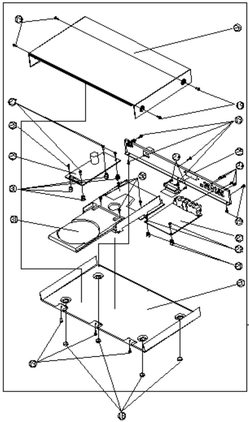
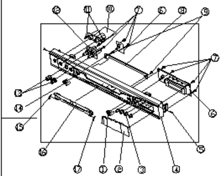
8.CIRCUIT DIAGRAMS
A. Index
ESCHER-H1 REV-A6
Layos-ECHER-HI REV-A88
ES66x8 + HOP1200 PICKUP + OUTPUT
Background
This DVD design is based on ESS Vibrio-1 ESS60d single chip DVD MPEG and video processor. The ESS60d is built upon ESS protein Programmable Multimedia Processor architecture with integrated video DSP. A complete DVD design using ESS6000 RF-Amp can support all major popular optical pickup heads. With ESS60d only memory architecture, the whole system memory is reduced to a minimum. ESS60d provides the best price performance DVD solution in the industry.
System Clock Requirement
ES0001 requires a 27MHz clock to operate. This 27MHz can either be generated externally and fixed into pin 3 and pin 4 or into a 27MHz crystal attached to pin 2 and 3. This 27MHz will be used for all video processing reference. In addition, internal multiplier will generate a much higher operating frequency for the internal RISC+DSP code to operate. Audio clock is generated from E5600 by its internal PLL circuitry.
SDRAM Usage
E5063 support the use of higher density 4w16 GDRAM. A single of 4w16 GDRAM is sufficient for the whole system to open.
System Configuration
| CHIP | FUNCTION |
| E95603 | Single chip processor that handles all system control, DVD decoding and video control. |
| 64MB EEPROM | Data storage and frame buffer |
| IMM1 EPROM/FLASH | Program storage |
| 2400 SERIAL EE | System setup configuration storage |
| VWNTSE | 2-Channel AudioDAC |
| VWNTHS | 6-Channel AudioDAC |
| VWNTSS | 2-Channel AudioACC |
| LC50# | FUNCTION |
| LC30# | ZFRAX |
| LC81# | TANGEST4 (U16) I/O EXPAND CONTROL |
| LC22# | NON EMULATOR |
| LC83# | NON/FLASH |
| ALIX | FUNCTION |
| AIX0 | IDC DATA |
| AIX1 | IDC CLOCK |
| AIX2 | NICKNAME / NAME |
| AIX3 | SCARTCTL / WNTC |
| AIX4 | IN |
| AIX5 | VFD DATA |
| AIX6 | VFD CR |
| AIX7 | VFD CLK |
| CAUXs | FUNCTION |
| KANFIO | ATSDCOAC MD |
| KANXOS | ATSDCOAC NC |
| KANXO2 | ATSDCOAC KG |
| KANXO3 | ATSDCOAC CBN |
| XGP10x | FUNCTION |
| XGP104 | MOCTL / K222C DET |
| XGP105 | DRVSW |
| XGP106 | COTON |
| XGP107 | CLOSE |
| XGP108 | NOREM |
| XGP109 | INHM |
Revision History
Aa
- Date on HQ ES0002 reference design and corresponding ES0003 reference design is form the schematics
A2
-
Change E0000 from 206 pins package to 216 pins package
-
Dase on HC's new gis assignmert,redite all the ples of ES06b6.
AaA
-
Restige AUXEAUX ples usage (AUX255, AUX234, AUX3012, AUX43)
-
Goup SLD+ and DCMo+ at 12
A
- Change back to 206-pin package again by reclassing XPGIO[0,3] from the servo side
A
1.Add pull low rederator R73 on TSD2
2.Delphi two ZERO circles
-
Charge DDQ 500 OPIN to N4148
-
Change R90 from % to OPEN
SAeLA201FASHand erubt
6ExchangePBandPR
A
1A6LUP111
2.Dae 039041045C5106108
3.00000000000000000000000000000000000000000000
4Cmred Pnnt pcky
5 Change nELAUXDO to ALUX42,ALUXH to ALUX41,ALUX02 to ALUX42,ALUX03 to ALUX43.
Change start index from 1p in to 1p in add two control signals and a power VDC.
- Are pull_high reactor RNA
| ESS TECHNOLOGY, INC. | ||
| ### | ### | ### |
| ### | ### | ### |
| ### | ### | ### |
B. Vibratto-II ES66x8
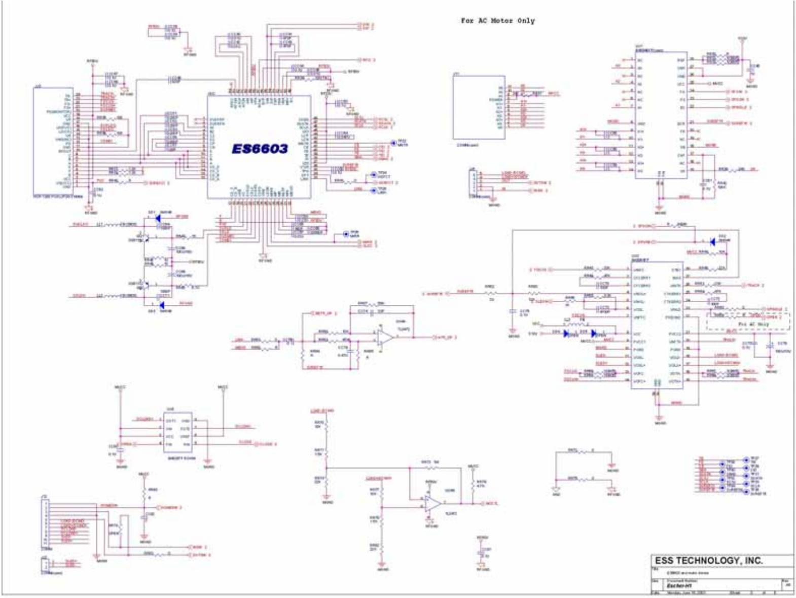
C.Motor Drives
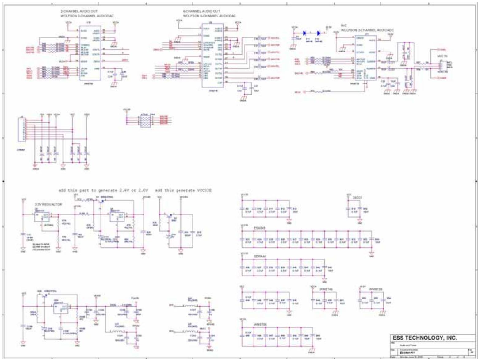
D. Audio and Power
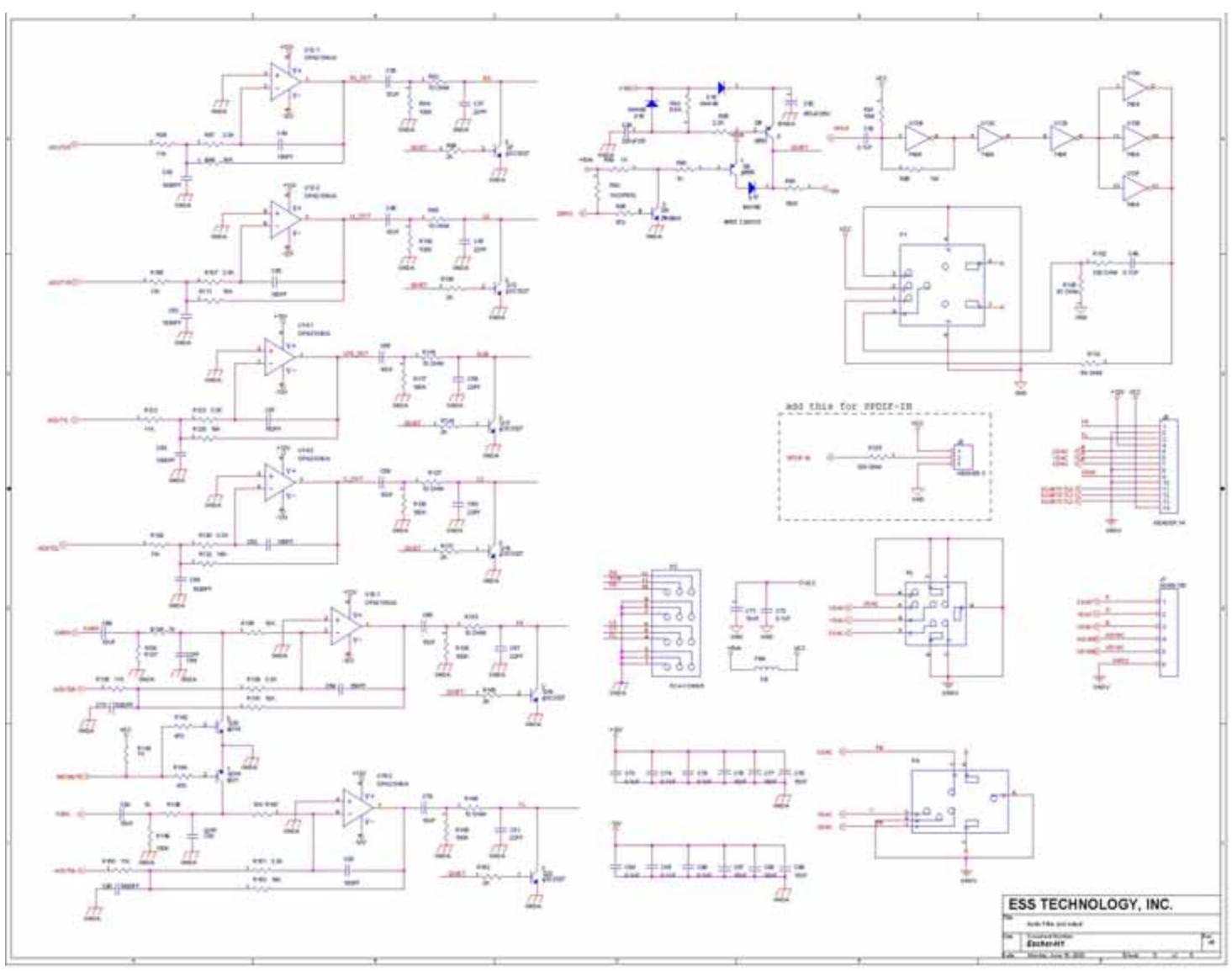
E. Audio Filter and output
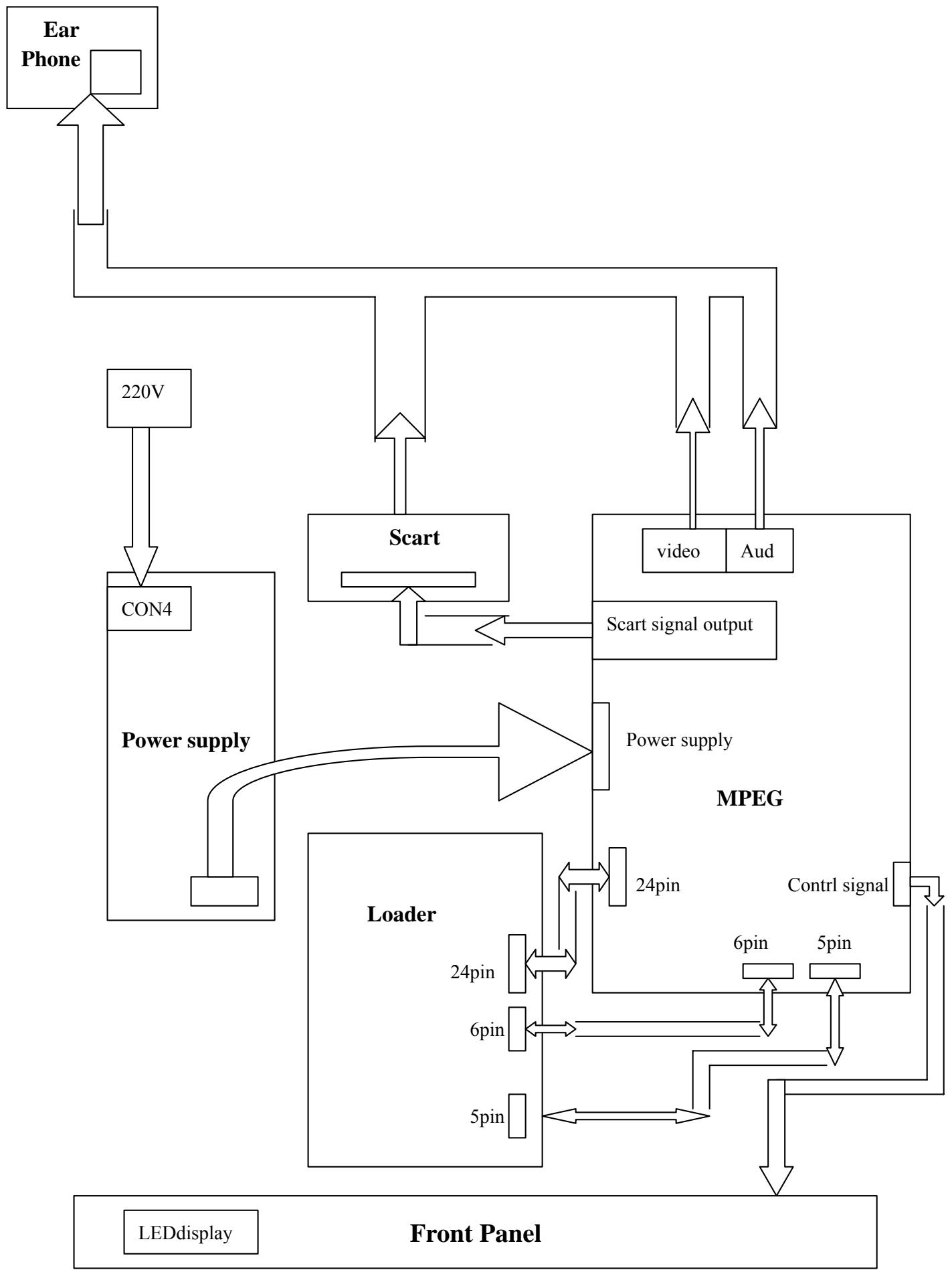
8.WIRING DIAGRAM
- DVD-2506X
- DEUTSCH
- On Screen Display
- Input / Output
- General
- CONTENTS :
- 1.INFORMATIONS
- Vibratto-II DVD Processor (ESS 66x8)
- FEATURES:
- 2.OPERATING INSTRUCTIONS
- GENERAL SETUP
- a.TV DISPLAY
- b. PIC MODE (PICTURE MODE)
- (FOR PROGRESSIVE-SCAN MODEL)
- c.ANGLE MARK
- This feature is functioned only for the disc, which has ANGLE function:
- d. OSD LANG (ON SCREEN DISPLAY LANGUAGE)
- e. CAPTIONS
- f. SCR SAVER
- 2.SPEAKER SETUP
- a. DOWNMIX
- b. CENTER
- d. SUBWOOFER
- e. CNTR DELAY
- f. REAR DELAY
- g. TEST TONE
- 3.AUDIO SETUP
- i. DEFLAUTS
- j. SMART NAVI
- JPEG, MP3 & MPEG4 Format
- FUNCTION KEYS
- 3.PRODUCT SPECIFICATIONS
- 4.TROUBLESHOOTING
- 5.MAINTENACF INSTRUCTIONS
- INDEX
- 6.ELECTRICAL PART LIST
- 7.DISASSEMBLY AND REASSEMBLY
- 8.CIRCUIT DIAGRAMS
- Index
- ESCHER-H1 REV-A6
- ES66x8 + HOP1200 PICKUP + OUTPUT
- Background
- System Clock Requirement
- SDRAM Usage
- Revision History
- Vibratto-II ES66x8
- C.Motor Drives
- Audio and Power
- Audio Filter and output
- 8.WIRING DIAGRAM
Brand : ROADSTAR
Model : DVD-2506X
Category : DVD player