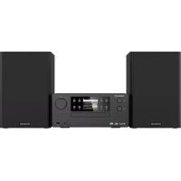
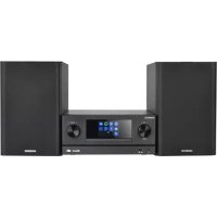
XD-501 - Audio System KENWOOD - Free user manual and instructions
Find the device manual for free XD-501 KENWOOD in PDF.
| Product Type | Audio system with CD player, dual cassette deck and FM/AM tuner |
| Brand | KENWOOD |
| Model | XD-501 |
| Dimensions (W x H x D) | 420 x 130 x 280 mm |
| Weight | 5.2 kg |
| Power Supply | 230 V ~ 50 Hz |
| Power Consumption | 60 W |
| Output Power | 2 x 30 W RMS |
| Main Functions | CD player, dual cassette deck (A/B), FM/AM tuner with 30 presets, Echo effect, Sleep timer |
| Connections | Auxiliary input (RCA), headphone output (6.35 mm), FM/AM antenna |
| Display | Segment display with function indicators |
| Maintenance and Cleaning | Clean with a soft, dry cloth. Do not use abrasive products or solvents. |
| Safety | Unplug the device before any cleaning. Do not expose to moisture or heat sources. |
| Spare Parts and Repairability | Contact Kenwood after-sales service for spare parts and repairs. |
| General Information | Manual available in multiple languages. Approximate weight and dimensions. |
Frequently Asked Questions - XD-501 KENWOOD
User questions about XD-501 KENWOOD
0 question about this device. Answer the ones you know or ask your own.
Ask a new question about this device
Download the instructions for your Audio System in PDF format for free! Find your manual XD-501 - KENWOOD and take your electronic device back in hand. On this page are published all the documents necessary for the use of your device. XD-501 by KENWOOD.
USER MANUAL XD-501 KENWOOD
**Refer to page 2 if you want to know system configuration.
In compliance with Federal Regulations, following are reproductions of labels on, or inside the product relating to laser product safety.
Refer to RXD-500/700 (B51-5300-00), If you require TUNER preset frequency in detail.
- Refer to parts list on page 58.
KENWOOD-Crop. certifies this equipment conforms to DHHS Regulations No. 21 DFR 1040.10, Chapter 1, Subchapter J.
DANGER : Laser radiation when open and interlock defeated. AVOID DIRECT EXPOSURE TO BEAM
CONTENTS / ACCESSORIES
Contents
CONTENTS / ACCESSORIES 2
EXTERNAL VIEW 3
DISASSEMBLY FOR REPAIR. 4
BLOCKDIAGRAM 5
CIRCUIT DESCRIPTION. 6
ADJUSTMENT 13
WIRING DIAGRAM 17
WIRING DIAGRAM 17
PC BOARD 19
SCHEMATIC DIAGRAM 27
EXPLODED VIEW 55
PARTS LIST 58
SPECIFICATIONS .Back cover
Accessories
FM Indoor antenna
(T90-0801-05): KPXYMM2
(T90-0836-05): TEQE2
Speaker cords (4)
XD-A8/XD-7....Series
Speaker cords (2)
XD-A5/XD-5....Series

Attached with to speaker unit
Batteries (R6/AA)

Speaker cushion (8)
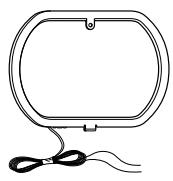
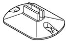
AM Loop antenna (T90-0833-05)
AM Loop antenna stand (J19-3645-05)
AC plug adaptor (1)
(E03-0115-05)
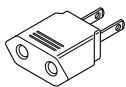
Use to adapt the plug on the power cord to the shape of the wall outlet.
(Accessory only for regions where use is necessary.)
Remote control unit (1)
(A70-1201-05) :KPMXYM2
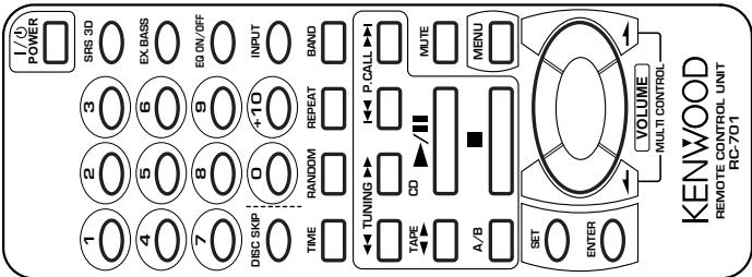
Battery cover (A09-0399-08)
Remote control unit (1)
(A70-1202-05) : QETE2
Battery cover (A09-0399-08)
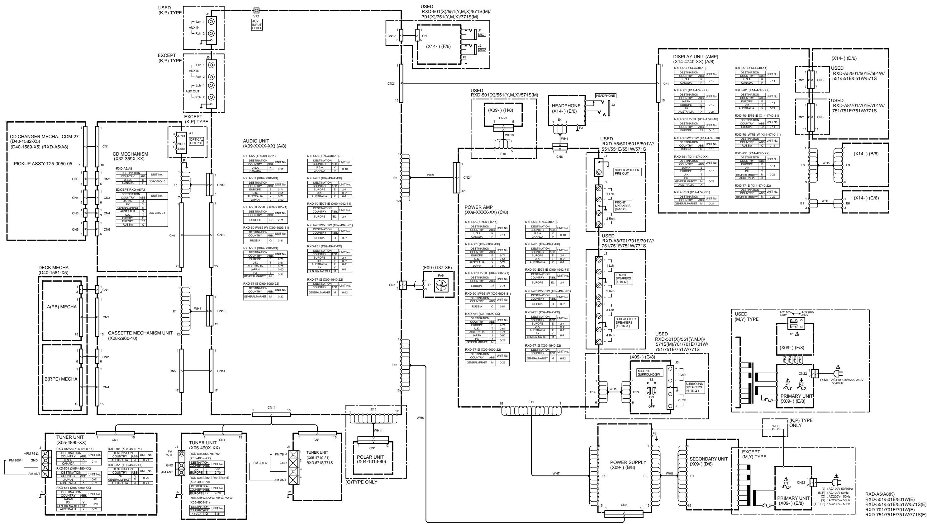
System configuration
| SYSTEM | MAIN UNIT | SPEAKER | SP CORD PARTS NO. | DESTI- NATION |
| XD-501 | RXD-501 | LS-501 | E30-5474-08 | TE |
| XD-501 | RXD-501 | LS-501 | E30-5475-05 | X |
| XD-501W | RXD-501W | LS-501 | E30-5474-08 | Q |
| XD-501E | RXD-501E | LS-501 | E30-5474-08 | E2 |
| XD-551 | RXD-551 | LS-551 | E30-5475-05 | MXY |
| XD-551 | RXD-551 | LS-551 | E30-5474-08 | TE |
| XD-551W | RXD-551W | LS-551 | E30-5474-08 | Q |
| XD-551E | RXD-551E | LS-551 | E30-5474-08 | E2 |
| XD-571S | RXD-571S | LS-551 | E30-5475-05 | M2 |
| SYSTEM | MAIN UNIT | SPEAKER | SP CORD PARTS NO. | DESTI- NATION |
| XD-A5 | RXD-A5 | LS-451 | E30-5120-08 | KP |
| XD-701 | RXD-701 | LS-701 | E30-5471-05 | TEX |
| XD-701W | RXD-701W | LS-701 | E30-5471-05 | Q |
| XD-701E | RXD-701E | LS-701 | E30-5471-05 | E2 |
| XD-751 | RXD-751 | LS-751 | E30-5471-05 | MXYTE |
| XD-751W | RXD-751W | LS-751 | E30-5471-05 | Q |
| XD-751E | RXD-751E | LS-751 | E30-5471-05 | E2 |
| XD-771S | RXD-771S | LS-751 | E30-5471-05 | M2 |
| XD-A8 | RXD-A8 | LS-751 | E30-5471-05 | KP |
1-1 Setting of initial conditions
While pressing the [ENTER] key, plug the AC cord into the AC power outlet.
1-2 Initializing operation
- A microcomputer is initialized for start when the AC power is turned on while pressing the [ENTER] key. At that time, CD mechanism and CASSETTE mechanism are also initialized.
- During the initial operation, the display shows "INITIALIZE" and after that the clock blinks up on display.
1-3 Initial items and back up data
| ITEMS | ||
| AMP | POWER | OFF |
| VOLUME | 45 | |
| BALANCE | CENTER | |
| MUTING | OFF | |
| EQ | OFF (ROCK) | |
| EQ. MANU | FLAT | |
| EX. BASS | ON | |
| SRS 3D | OFF | |
| S.W. | LEVEL 3 (RXD-701/751 ONLY) | |
| INPUT SEL | TUNER | |
| 3D LEVEL | LEVEL +5 | |
| DEMO | ON | |
| TUNER | BAND | FM |
| LAST f | LOWEST FREQUENCY | |
| LAST Pch | —— | |
| AUTO/MONO | AUTO | |
| Pch | TEST f | |
| CLOCK TIMER | CLOCK | AM 12:00 |
| PROG ON | AM 12:00 | |
| PROG OFF | AM 12:00 | |
| PRO MODE | TIMER PLAY | |
| SOURCE | TUNER | |
| Pch | 1 | |
| EXE | OFF | |
| OTT | OFF | |
| SLEEP | OFF | |
| DECK | DIRECTION | FORWARD |
| RVS MODE | □ | |
| DOLBY NR | OFF | |
| A/B | B | |
| ACTIVE MODE | STOP | |
| CD | PLAY MODE | TRACK |
| REPEAT | OFF | |
| RANDOM | OFF | |
| PLAY MODE | STOP | |
| TIME | SINGLE | |
back up data
1-4 Mechanism initialization
1-4-1 CD mechanism
- Disc unclamps (traverse down)
- Rotary tray rotates (1/3 rotation)
- If a mechanism error occurs, "C" is indicated on the display.
1-4-2 DECK mechanism
- When initial condition becomes NG for the third time, decide the error.
The error condition is displayed as "X" on the display.
1-4-3 Error display
CD X ERR
CIRCUIT DESCRIPTION
2. Destination list of tuner
| Desti-nation | DSW | Band | Receiving frequency range | Channel space | IF | RF | PORT 47 | |||
| 3(83pin) | 2(84pin) | 1(85pin) | (86pin) | |||||||
| K1 | 0 | 0 | 0 | 0 | FM | 87.5MHz~108.0MHz | 100kHz | +10.7MHz | 25kHz | 0 |
| AM | 530kHz~1700kHz | 10kHz | +450kHz | 10kHz | 0 | |||||
| K2 | 0 | 0 | 0 | 1 | FM | 87.5MHz~108.0MHz | 100kHz | +10.7MHz | 25kHz | 1 |
| AM | 530kHz~1610kHz | 10kHz | +450kHz | 10kHz | 0 | |||||
| K3 | 1 | 0 | 0 | 1 | FM | 87.5MHz~108.0MHz | 100kHz | +10.7MHz | 25kHz | 1 |
| MW | 530kHz~1610kHz | 10kHz | +450kHz | 10kHz | 0 | |||||
| SW | 5.9MHz~17.9MHz | 5kHz | +450kHz | 5kHz | 0 | |||||
| E1 | 0 | 0 | 1 | 1 | FM | 87.5MHz~108.0MHz | 50kHz | +10.7MHz | 25kHz | 0 |
| AM | 531kHz~1602kHz | 9kHz | +450kHz | 9kHz | 0 | |||||
| E3 | 1 | 0 | 1 | 1 | FM | 87.5MHz~108.0MHz | 50kHz | +10.7MHz | 25kHz | 0 |
| MW | 531kHz~1602kHz | 9kHz | +450kHz | 9kHz | 0 | |||||
| SW | 5.9MHz~17.9MHz | 5kHz | +450kHz | 5kHz | 0 | |||||
| E1RDS | 0 | 1 | 0 | 1 | FM | 87.5MHz~108.0MHz | 50kHz | +10.7MHz | 25kHz | 0 |
| AM | 531kHz~1602kHz | 9kHz | +450kHz | 9kHz | 0 | |||||
| E2RDS | 0 | 1 | 1 | 0 | FM | 87.5MHz~108.0MHz | 50kHz | +10.7MHz | 25kHz | 0 |
| MW | 531kHz~1602kHz | 9kHz | +450kHz | 9kHz | 0 | |||||
| LW | 153kHz~279kHz | 9kHz | +450kHz | 9kHz | 0 | |||||
| Q | 0 | 1 | 1 | 1 | FML | 65.0MHz~74.0MHz | 10kHz | +10.7MHz | 5kHz | 1 |
| FMH | 87.5MHz~108.0MHz | 50kHz | +10.7MHz | 5kHz | 0 | |||||
| MW | 531kHz~1602kHz | 9kHz | +450kHz | 9kHz | 0 | |||||
| LW | 153kHz~279kHz | 9kHz | +450kHz | 9kHz | 0 | |||||
3. Test mode
3-1 Test mode of the receiver
3-1-1 Setting of the test mode
While pressing the [INPUT] key or [Band] key, plug the AC power cord into AC outlet.
3-1-2 Canceling of the test mode
Unplug the AC power cord.
3-1-3 Condition in test mode
POWER ON
SELECTOR AUX (in case of [INPUT] key)
TUNER (in case of [BAND] key)
FL, LED All the fluorescent display indicators and LEDs light. (The all illuminated state is cleared by pressing any main unit key or remocon key.
EX.BASS OFF S.W. OFF
3-1-4 Basic operation in test mode.
(1) The muting during mode selection is not controlled in the test mode.
(2) The test mode is cancelled when the AC power is turned OFF.
(3) The operation of the keys in the test mode, as follows.
3-1-5 The operation of the keys in the test mode.
(1) MODE / DEMO key When this key is pressed in the test mode, all the fluorescent light off and normal display are indicated cyclically.
(2) DISC 1~3 keys
With the selector on AUX, when the DISC 1~3 keys are operated, the 3D level settings can be made as follows.
① DISC 1···3D ON level -8 (Min)
② DISC 2···3D ON level 0 (Center)
③ DISC 3···3D ON level +8 (Max)
(3) DISC SKIP key (S level display)
With the selector on TUNER, the fluorescent changes cyclically as follows by pressing the [DISC SKIP] key.
① ATT is switched OFF. “ATT OFF XX”
② ATT is switched ON. “ATT ON XX”
③ ATT is switched OFF. Normal display XX means A/D value (HEX) of S
(4) CD STOP key
With the selector on TUNER, when the [CD STOP] key operated, the preset memory can be changed as 10 steps.

(5) AUTO, TUNING UP/DOWN
With the selector on something other than TUNER, the E.Q (Flat, Min, Max) settings can be made by pressing the [AUTO] key and the tuning [UP] [DOWN] keys.
[AUTO] key E.Q Flat
TUNING [DOWN] key E.Q Min
TUNING [UP] key E.Q Max
CIRCUIT DESCRIPTION
(6) CD SKIP UP/DOWN keys
With the selector on TUNER, the P. CALL is operated by pressing the skip UP/DOWN keys.
SKIP [UP] key
P.CALL up
SKIP [DOWN] key
P. CALL down
(7) CD OPEN/CLOSE keys
With the selector on TUNER, the channel space settings can be mad cyclically by pressing the OPEN/CLOSE keys with M version.
(8)REC/ARM
Whenever the REC/ARM key is pressed, the indication of S.W. (ON/OFF) is available.
4. Main microprocessor
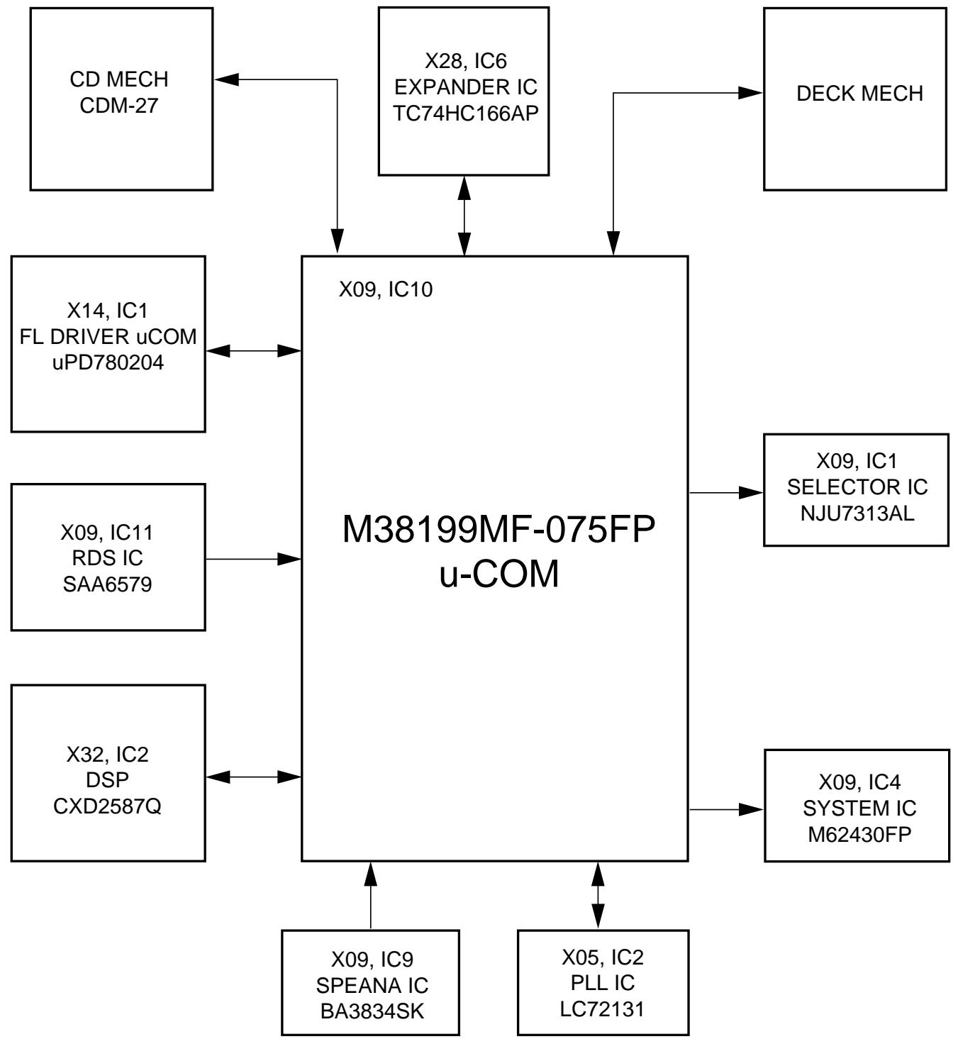
4-1 Microprocessor periphery block diagram
CIRCUIT DESCRIPTION
4-2 Pin description
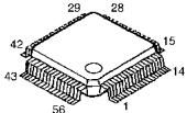
Microprocessor : M38199MF-075FP (X09, IC10)
| No | Name | I/O | Description | ||
| 1 | PS IN | I | Parallel serial IC input data | ||
| 2 | PS LOAD | O | Parallel serial IC load | H:SHIFT | L:LOAD |
| 3 | A MUTE | O | Audio mute control | H:OFF | L:ON |
| 4 | BP IN | I | Speana input (A/D converter input) | ||
| 5 | JOG CW | I | Jog input B | ||
| 6 | JOG CCW | I | Jog input A | ||
| 7 | ENC CW | I | Rotary encoder input B | ||
| 8 | ENC CCW | I | Rotary encoder input A | ||
| 9 | H.P. | I | Headphones switch input | H:ON | L:OFF |
| 10 | NC | I/O | No used | ||
| 11 | CD RST | O | CD DSP IC reset control (CXD2587Q) | H:NORMAL | L:RESET |
| 12 | DRV CLK | O | FL driver u-COM control clock | ||
| 13 | DRV SI | O | FL driver u-COM control data output | ||
| 14 | DRV SO | I | FL driver u-COM control data input | ||
| 15 | S LEVEL | I | RDS S Level input | ||
| 16 | RDS DATA | I | RDS data input | ||
| 17,18 | NC | I | No used | ||
| 19 | CD CK | O | CD DSP IC clock (CXD2587Q) | ||
| 20 | SQCK | O | CD Sub code clock (CXD2587Q) | ||
| 21 | CDDT | O | CD DSP IC data (CXD2587Q) | ||
| 22 | SQSO | I | CD Sub code input (CXD2587Q) | ||
| 23 | CDXL | O | CD latch output (CXD2587Q) | ||
| 24 | SENS | I | CD sense input (CXD2587Q) | ||
| 25 | CDSCK | O | Sense data reading clock output (CXD2587Q) | ||
| 26 | LD ON | O | CD laser output | H:OFF | L:ON |
| 27 | DATA | O | SELECTOR/SYSTEM/DAC/DOLBY IC data output | ||
| 28 | CLK | O | SELECTOR/SYSTEM/DAC/DOLBY IC clock output | ||
| 29 | PROT | I | Protection input | H:PROTECTION ON | L:NORMAL |
| 30 | SCOR | I | Sub code synchronism signal (CXD2587Q) | ||
| 31 | E DATA | O | E. vol data output (M62430FP) | ||
| 32 | E CLK | O | E. vol clock output (M62430FP) | ||
| 33 | NC | I/O | No used | ||
| 34 | RDS CLK | I | RDS clock input | ||
| 35 | RESET | I | Reset signal input | H:NORMAL | L:RESET |
| 36 | X CIN | I | Timer clock input (32.768kHz) | ||
| 37 | X COUT | O | Timer clock output (32.768kHz) | ||
| 38 | X IN | I | Main clock input (8.38MHz) | ||
| 39 | X OUT | O | Main clock output (8.38MHz) | ||
| 40 | VSS | - | GND | ||
| 41 | PLL DO | I | PLL data input | ||
| 42 | STEREO | I | Stereo detector input | ||
| 43 | SD | I | SD detector input | ||
| 44 | CE | I | Power failure input | H:AC ON | L:AC OFF |
| 45 | PLL CE | O | PLL IC chip enable (LC72131) | ||
| 46 | TU EMP | O | FM emphasis change-over (M type only) | H:100kHz | L:50kHz |
| Polar/Pilot change-over (Q type only) | H:POLAR | L:PILOT | |||
| 47 | FL RST | O | FL driver reset control output | ||
CIRCUIT DESCRIPTION
| No | Name | I/O | Description | ||
| 48 | T MUTE | O | TUNER mute control output | ||
| 49 | DRV ST | O | FL driver u-COM control strobe output | ||
| 50 | HP RLY | O | Headphones relay control | ||
| 51 | SEL ST | O | Selector IC strobe output (NJU7313AL) | ||
| 52 | ATT | O | E. vol attenuation | H : ON | L : OFF |
| 53 | SYS ST | O | System IC strobe output (M62430FP) | ||
| 54 | CS RELAY | O | CS speaker relay control | H : ON | L : OFF |
| 55 | SP RELAY | O | Speaker relay control | H : ON | L : OFF |
| 56 | DOL ST | O | Dolby IC strobe output | ||
| 57 | MON | O | PMON control | H : ON | L : OFF |
| 58~61 | NC | O | No used | ||
| 62 | P RLY | O | Power relay control | H : ON | L : OFF |
| 63 | LMR | O | Loading motor control (reverse) | ||
| 64 | LMF | O | Loading motor control (forward) | H : ON | L : OFF |
| 65 | RMF | O | Rotary motor control (forward) | H : ON | L : OFF |
| 66 | BRKM | O | Rotary motor control (brake) | H : NORMAL | L : BRAKE |
| 67 | RMR | O | Rotary motor control (reverse) | H : ON | L : OFF |
| 68 | DC OFF | O | CD DSP IC power control (CXD2587Q) | H : ON | L : OFF |
| 69 | BEAT CANCEL | O | Beat cancel | H : ON | L : OFF |
| 70 | A/B | O | A/B Playback change-over | H : B | L : A |
| 71 | BIAS | O | Bias change-over | H : ON | L : OFF |
| 72 | R MUTE | O | Deck rec mute control | H : OFF | L : ON |
| 73 | NR | O | Dolby noise reduction change-over | H : ON | L : OFF |
| 74 | D-R/P | O | Dolby rec/play change-over | H : REC | L : PLAY |
| 75 | R/P | O | Rec/play change-over | H : REC | L : PLAY |
| 76 | B CPM | O | B deck motor control | H : ON | L : OFF |
| 77 | B SOL | O | B deck solenoid control | H : ON | L : OFF |
| 78 | A CPM | O | A deck motor control | H : ON | L : OFF |
| 79 | A SOL | O | A deck solenoid control | H : ON | L : OFF |
| 80 | SPE3 | O | Speana out 3 | ||
| 81 | TU/SPE2 | O | TUNER destination (scan)/speana out 2 | ||
| 82 | TYP/SPE1 | O | Model discrimination (scan)/speana out1 | ||
| 83~86 | RET4~RET1 | I | Model discrimination input 4~1 Discrimination of TUNER destination (DSW3~DSW0) | ||
| 87 | A-PH | I | A deck photo sensor input | ||
| 88 | B-PH | I | B deck photo sensor input | ||
| 89 | UNL SW | I | CD unload switch | H : ON | L : OFF |
| 90 | LO SW | I | CD load switch | H : OFF | L : ON |
| 91 | VCC | - | u-COM power supply (+5V) | ||
| 92 | ST SW | I | CD mechanism stop switch | H : OFF | L : ON |
| 93 | UP SW | I | CD mechanism up switch | H : OFF | L : ON |
| 94 | DN SW | I | CD mechanism down switch | H : OFF | L : ON |
| 95 | PS SW | I | CD mechanism position switch | H : OFF | L : ON |
| 96 | CD MUT | O | CD analog mute | H : OFF | L : ON |
| 97 | ZERO | I | CD zero mute detection | H : MUTE OFF | L : MUTE ON |
| 98 | VEE | - | GND | ||
| 99 | AVSS | - | A/D GND | ||
| 100 | VREF | - | A/D reference voltage | ||
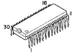
5. FL driver Microprocessor : uPD780204-038 (X14, IC1)
5-1Pin description
| No | Name | I/O | Description |
| 1 | VDD | - | u-COM power supply (+5V) |
| 2 | LED DISC1 | O | Disc LED 1~3 control |
| 3,4 | NC | - | No used |
| 5~9 | LED A~E | O | CD running indicator control (D33~D37) |
| 10 | RESET | I | System reset |
| 11 | X2 | - | Main system clock (5MHz) |
| 12 | X1 | I | Main system clock (5MHz) |
| 13 | VSS | - | GND |
| 14 | NC | - | No used |
| 15 | NC | - | GND |
| 16 | VDD | - | u-COM power supply (+5V) |
| 17 | DRIVER CLK | I | Serial clock |
| 18 | DRIVER SOUT | O | Serial data output |
| 19 | SIN | I | Serial data input |
| 20,21 | NC | - | No used |
| 22 | LED SRS | O | LED control terminal (SRS) |
| 23 | LED 3 STEREO | - | No used |
| 24 | LED PROLOGIC | - | No used |
| 25 | AVSS | - | GND |
| 26 | A/D7 | - | GND |
| 27~33 | A/D6~A/D0 | I | Key return signal (6~0) |
| 34 | AVDD | - | A/D power supply |
| 35 | AVREF | - | A/D reference voltage |
| 36,37 | NC | - | GND |
| 38 | REM IN | I | Remocon signal input |
| 39 | DRIVER ST | I | Strobe signal input |
| 40 | VSS | - | GND |
| 41 | LED EQ | O | LED control terminal (SOUND) |
| 42~44 | ECHO 3~1 | - | No used |
| 45 | ECHO MUTE | - | No used |
| 46 | VDD | - | u-COM power supply (+5V) |
| 47 | NC | - | No used |
| 48~63 | SEG16~SEG1 | O | FL segment control (SEG16~SEG1) |
| 64~70 | SEG17~SEG23 | O | FL segment control (SEG17~SEG23) |
| 71~78 | SEG24~SEG31 | O | FL segment control (SEG24~SEG31) |
| 79 | VLOAD | - | Vload (-30V) |
| 80~88 | SEG32~SEG40 | O | FL segment control (SEG32~SEG40) |
| 89~100 | 1G~12G | O | FL grid control (1G~12G) |
CIRCUIT DESCRIPTION
6. Input expander IC (parallel-serial)
X28, IC6 (TC74HC166AP)
| Pin No. | Name | I/O | Description | ||
| 1 | - | I | +5V | ||
| 2 | - | I | N. C. | ||
| 3 | DPSS | I | DECK DPSS DETECTION | H = MUSIC | L = NO MUSIC |
| 4 | A-PLAY | I | A DECK PLAY SW | H = NOT PLAY | L = PLAY |
| 5 | A-PACK | I | A DECK PACK DETECTION | H = PACK OUT | L = PACK IN |
| 6 | - | I | GND | ||
| 7 | CD CLK | I | CD CLOCK INPUT | ||
| 8 | GND | I | GND | ||
| 9 | - | I | +5V | ||
| 10 | B-PACK | I | B DECK PACK DETECTION | H = PACK OUT | L = PACK IN |
| 11 | B-PLAY | I | B DECK PLAY SW | H = NOT PLAY | L = PLAY |
| 12 | R REC | I | REVERSE REC DETECTION | H = REC PROHIBITION | L = REC PERMITTED |
| 13 | PS IN | I | PS IN | ||
| 14 | F REC | I | FORWARD REC DETECTION | H = REC PROHIBITION | L = REC PERMITTED |
| 15 | PS LOAD | I | PS LOAD | ||
| 16 | Vcc | I | +5V | ||
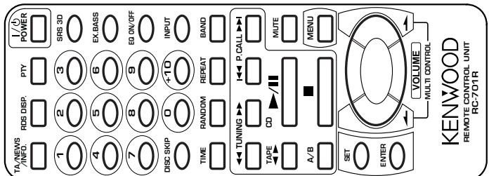
7. Key matrix
FL driver u-COM (uPD780204-038)
X14, IC1
| VOLTAGE (V) | AD0 (33pin) | AD1 (32pin) | AD2 (31pin) | AD3 (30pin) |
| 0 ~ 0.82 | POWER | EX. BASS | CD PGM | TUNING UP |
| 0.84 ~ 1.64 | - | - | DUBBING | TUNING DOWN |
| 1.66 ~ 2.52 | - | DISPLAY | SRS | BAND |
| 2.54 ~ 3.38 | - | INPUT | SOUND | AUTO |
| 3.40 ~ 4.18 | - | MODE / DEMO | SET | ENTER |
| 4.20 ~ 4.78 | - | TIMER | - | - |
| VOLTAGE (V) | AD4 (29pin) | AD5 (28pin) | AD6 (27pin) |
| 0 ~ 0.82 | CD ↓ | A / B | DOLBY NR |
| 0.84 ~ 1.64 | CD ▷ ↓ | TAPE ▷ | REV MODE |
| 1.66 ~ 2.52 | CD ■ | TAPE ▷ | DISC 1 |
| 2.54 ~ 3.38 | CD ▷ / II | TAPE ■ | DISC SKIP |
| 3.40 ~ 4.18 | CD ▲ | TAPE ▷ | DISC 2 |
| 4.20 ~ 4.78 | TAPE ● | TAPE ▷ | DISC 3 |
ADJUSTMENT
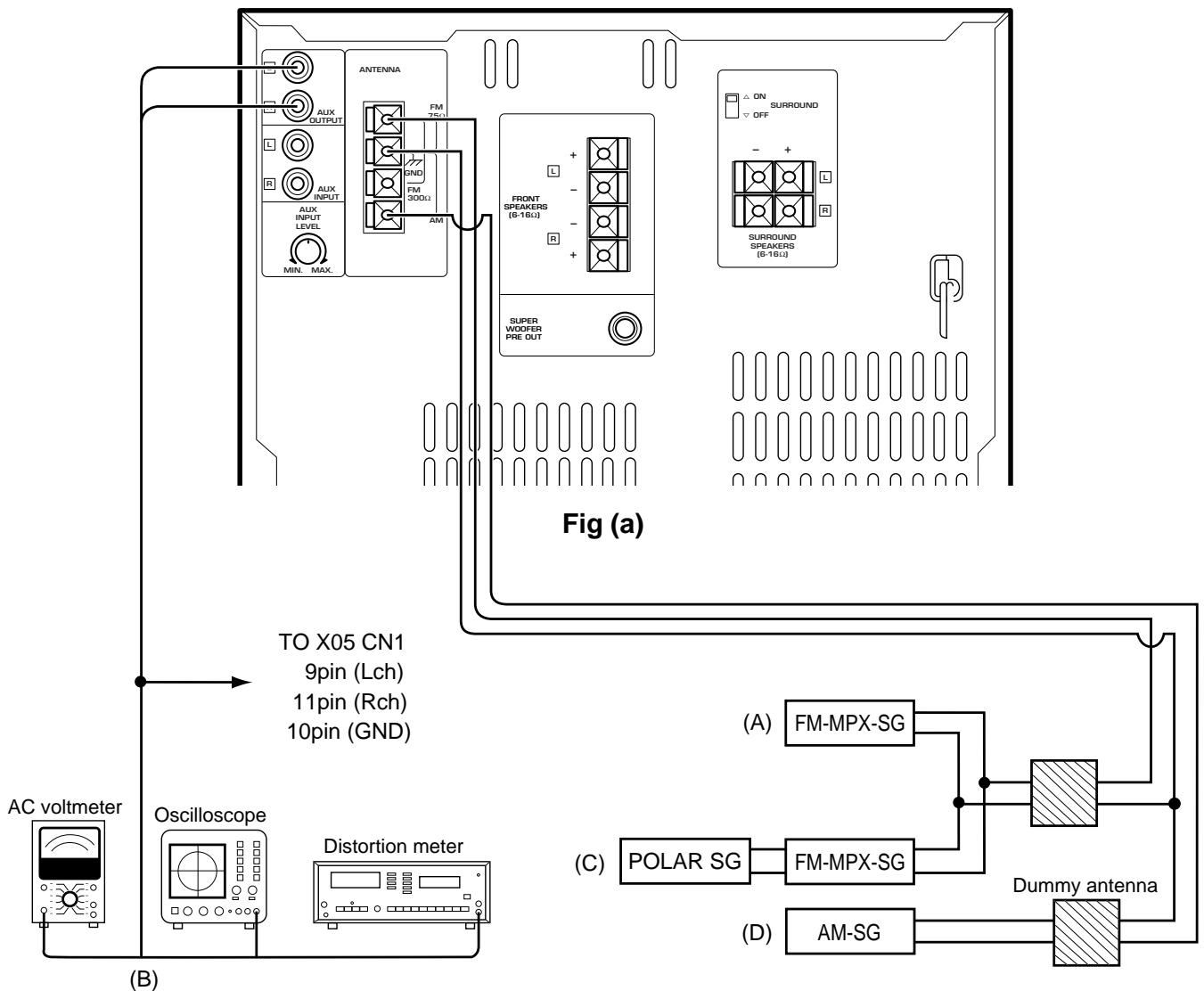
1. Tuner adjustment
X05-490x
| NO. | ITEM | INPUT SETTINGS | OUTPUT SETTINGS | TUNER SETTINGS | ALIGNMENTPOINTS | ALIGN FOR | FIG. |
| 1 | DISCRIMINATOR | (A)98 MHZ,70dBf (ANT INPUT)1 kHz, ±40 kHz DEV | Connect a DC voltmeter between pin 1 and pin2 of CN2. | MONO98.0 MHz | L31 | 0V | (a) |
| DISTORTION | L32(EXCEPT K/P) | Minimumdistortion. | |||||
| 2 | DISTORTION(STEREO) | (C)98 MHZ,70dBf (ANT INPUT)1 kHz, ±40 kHz DEV | (B) | AUTO98.0 MHz | IFT (A1) | Minimumdistortion. | (a) |
X05-4890
| NO. | ITEM | INPUT SETTINGS | OUTPUT SETTINGS | TUNER SETTINGS | ALIGNMENTPOINTS | ALIGN FOR | FIG. |
| 1 | TUNED LEVEL | (A)98 MHz,31.2dBf (ANT INPUT)1 kHz, ±40 kHz DEV | MONO98.0 MHz | VR1 | Adjust VR1 and stop at the point where ED1 (TUNED) goes ON. | (a) | |
| 2 | DISTORTION(STEREO) | (A)98 MHz,70dBf (ANT INPUT)1 kHz, ±40 kHz DEVPILOT: ±6 kHz DEV | (B) | AUTO98.0 MHz | IFT (A1) | Minimum distortion. | (a) |
X05-4710
| No. | ITEM | INPUT SETTING | OUTPUT SETTING | TUNER MODE | ALIGNMENT POINTS | ALIGN FOR | FIG. |
| 1 | DISCRIMINATOR | (A)98MHz1kHz, ±40kHzdev70dBf (ANT input) | Connect a DC voltmeter to CN2 | MONO98.0MHz | L5 | 0V | (a) |
| 2 | DISTORTION(STEREO) | (C)98MHz1kHz, ±40kHzdevPilot, ±6kHzdev70dBf (ANT input) | (B) | AUTO98.0MHz | IFT (A1) | Minimum distortion | (a) |
| 3 | SENSITIVITY(SW) | (D)6.5MHz400Hz 30%mod40dBf (ANT input) | (B) | 6.5MHz | L2 | Maximum output | (a) |
X04-1313 Q TYPE (65MHz~74MHz BAND)
| NO. | ITEM | INPUT SETTINGS | OUTPUT SETTINGS | TUNER SETTINGS | ALIGNMENTPOINTS | ALIGN FOR | FIG. |
| 1 | VCO | (E)69 MHz,70 dBf (ANT INPUT)1 kHz, 0 kHz DEVSUB, 0 kHz DEV | Connect a frequencycounter to VCO monitor(CN2). | AUTO69 MHz | VR 2 | Adjust it thefrequencycounterreads 31.25 kHz±100 Hz. | (a) |
| 2 | RESONANCEPOINT | (E)69 MHz,70 dBf (ANT INPUT)1 kHz, 40 kHz DEVSUB, 10 kHz DEVSelect : L or R | Connect a oscilloscopeto TUNER OUT(CN6). | AUTO69 MHz | TC 1 | Minimumcrosstalk. | (a) |
| 3 | SEPARATION | (E)SAME AS ABOVE | Connect a oscilloscopeto TUNER OUT(CN6). | AUTO69 MHz | VR 1 | Minimumcrosstalk. | (a) |
ADJUSTMENT
2. Test mode of CD player
2-1 Main unit
(1) Setting of the test mode While pressing the [PLAY/PAUSE] key, plug the AC power cord into AC outlet.
(2) Canceling of the test mode Press the [STOP] key on stop mode or unplug the AC power code from AC wall outlet.
(3) Operation
| KEY | DISPLAY | OPERATION |
| PLAY/PAUSE + AC IN | CD 00 | • SETTING OF THE TEST MODE • CANCEL THE CLAMP • TRAY1/3 ROTATION • TRAY OPENS AUTOMATICALLY |
| STOP■ | CD 00 | • TRAY CLOSE • CANCEL THE CLAMP |
| PLAY/PAUSE ▷/■ | CD 03 CD 05 | • TRAY CLOSE/DISC CLAMP • T-SERVO OFF(03) OR ON(05) |
| DISC SKIP | • TRAY 1/3ROTATION | |
| DISC 1 | 07 EF/FB 08 TG*FG 09 TE/RF 10 TE/VC | • MECHANISM STOPS WHEN THE AUTOMATIC ADJUSTMENT IS FINISHED. • DISPLAY CHANGES CYCLICALLY • IF NG, DISPLAY BLINKS UP |
ADJUSTMENT
3. Adjustment of CD player
| No. | ITEM | INPUT SETTING | OUTPUT SETTING | PLAYER SETTING | ALIGNMENT POINT | ALIGN FOR | FIG. |
| Step 1,2 are in TEST MODE TEST MODE: While pressing the [PALY/PAUSE] key, plug the AC power cord into the AC outlet. | |||||||
| 1 | LASER POWER | - | Set the senor section of the optical power meter on the pickup lens. | Press the"PLAY"key to check that the dis-play is "03". | - | On the power from.0.05 to 0.15mw. when the diffraction grating is correctly aligned with the RF level of 0.8Vp-p or more | (a) |
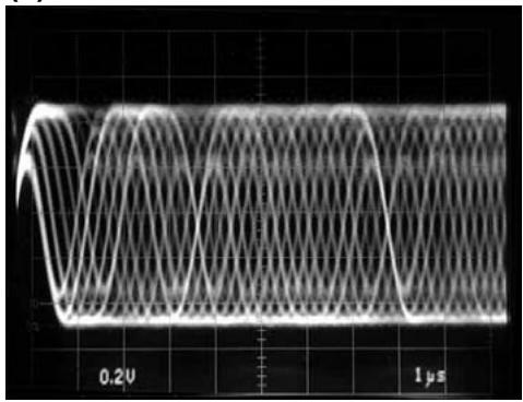
| 2 | FOCUS ERROR BALANCE | Test disc Type 4 | Connect an oscillo-scope as follows. CH1: RF(CN7 pin1) CH2: FE(CN7 pin6) GND: VC(CN7 pin4) | Press the "PLAY" key. Confirm that the display is "05" | FE BALANCE VR1 | Optimum eye pattern | (d) |
Note:
Type 4disc :SONY YEDS-18 Test Disc or equivalent. (KTD-02)
LPF : Around 47kΩ + 390pF or so.
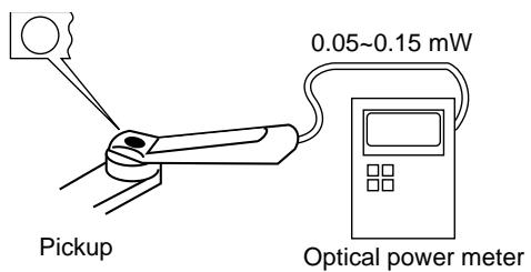
(a) Laser Power
(d)
RF signal : AC coupled
RF signal in test mode (PLAY).
- Perform the tangential and focusing offset are focused into one point on the display. The crossing points above and below the center shall also be looked clearly.
4. Test mode of DECK section
(1) Setting
While pressing the PLAY key(DECK), plug the AC power cord into an AC power outlet.
(2) Resetting
- Disconnect the AC power cord from an AC power outlet or press the [ON/STANDBY] key.
(3) Operation in TEST mode
(a) Initial condition
| Item | Condition |
| Power | ON |
| Selector | TAPE |
| Main VOL. | -45dB(VOL45) |
| EX. bass | OFF |
| FL, LED, LCD | All the FLs are turned on for 10 seconds |
(b) 4-sec REC
If the REC key is pushed, the system record for 4sec. Then, it rewrites to the REC starting position and plays back automatically.
If the REC key is pushed during the 4-sec REC operation, the system records further for 4-sec, then returns to the starting position of the first 4-sec REC operation and plays back.
(c) Mechanism SW detection
| SW | Display |
| B FWD REC Inhibit SW | CD Calendar (1) |
| B RVS REC Inhibit SW | CD Calendar (2) |
| A Pack SW | CD Calendar (3) |
| B Pack SW | CD Calendar (4) |
- Cassette Deck adjustment
| No | ITEM | INPUT SETTING | OUTPUT SETTING | DECK SETTING | ALIGNMENT POINT | ALIGN FOR | FIG. |
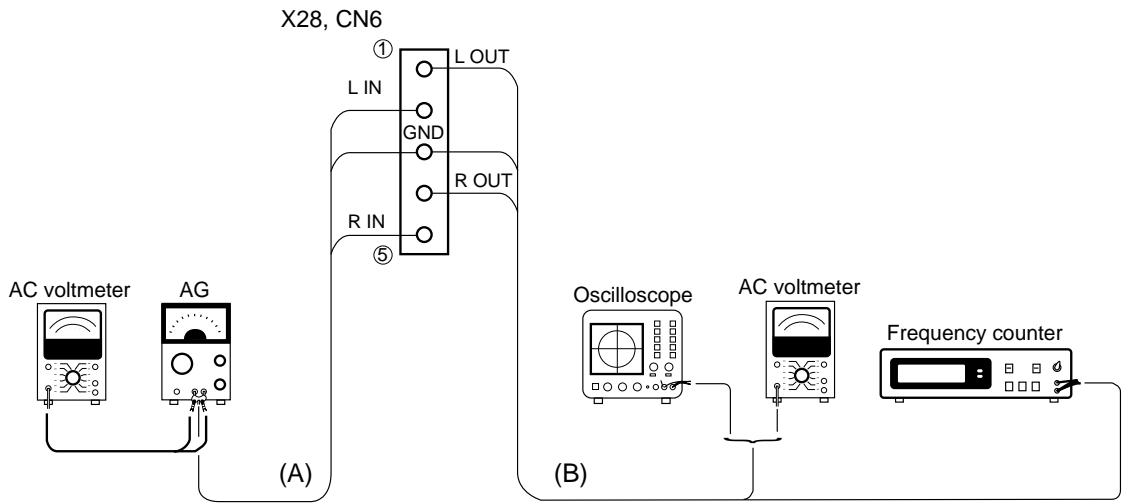
| Unless otherwise specified, set the respective switches as follows: 0dBs=0.775V TAPE : NORMAL DOLBY : OFF PLAY OUT : Lch (X28,CN6 ①pin), Rch (X28,CN6 ④pin) I . Cassette mechanism unit (Adjustment of the REC / PLAY head) | |||||||
| < 1 > | Demagnetization and cleaning | - | - | Power : OFF Demagnetiza- tion, cleaning, PLAY | Recording head, erase head, capstan pinch roller | Demagnetize the REC / PLAY head with the head eras- er. Clean the REC / PLAY head, erase head, capstan and pinch roller using a cotton swab slightly damped with alcohol. | |
| < 2 > | Azimuth of the REC/PLAY head | TCC-153 MTT-114 10kHz, -10dB | (B) | PLAY | FWD RVS | Adjust the output to maximum and adjust the azimuth adjust- ment screw for the Lissajours waveform pattern of the oscillo- scope to become close to a 45° straight line. | |
| II . PC BOARD ADJUSTMENT | |||||||
| < 1 > | TAPE SPEED(NORMAL) | TCC-110 MTT-111 SCC-1727 3kHz | (B) | PLAY | A DECK VR 5 B DECK VR 6 | Adjust the tape speed so that 3kHz is obtained at the center of the tape. | |
| III . PC BOARD ADJUSTMENT | |||||||
| < 1 > | PLAYBACK LEVEL | MTT- 150 400Hz | (B) | PLAY | A DECK VR 7 (L) VR 8 (R) B DECK VR 1 (L) VR 2 (R) | Adjust the playback output to -2.5dBs | |
| < 2 > | BIAS CURRENT | (A) Adjust the AG for the output of the DECK to become 400Hz (-20dB)/12.5kHz (-20dB) | (B) | REC ↑ PLAY | VR 3 (L) VR 4 (R) | Record 400Hz and 12.5kHz alternately, and adjust the bias current adjustment potentiometer for the playback levels to become the same. | |
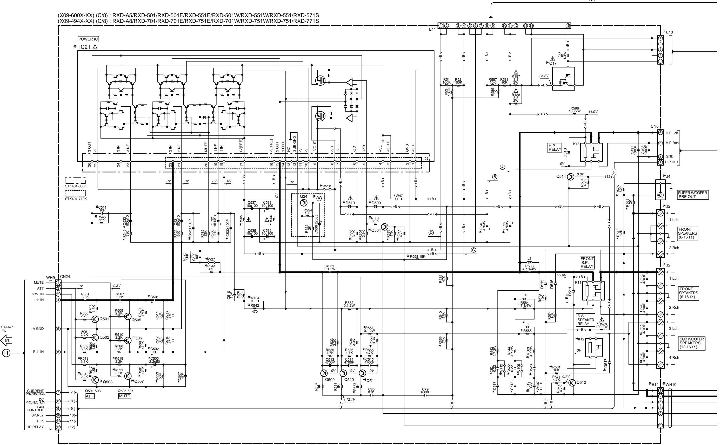
RXD-501/551/571/A5/701/751/771/A8 RXD-501/551/571/A5/701/751/771/A8
WIRING DIAGRAM
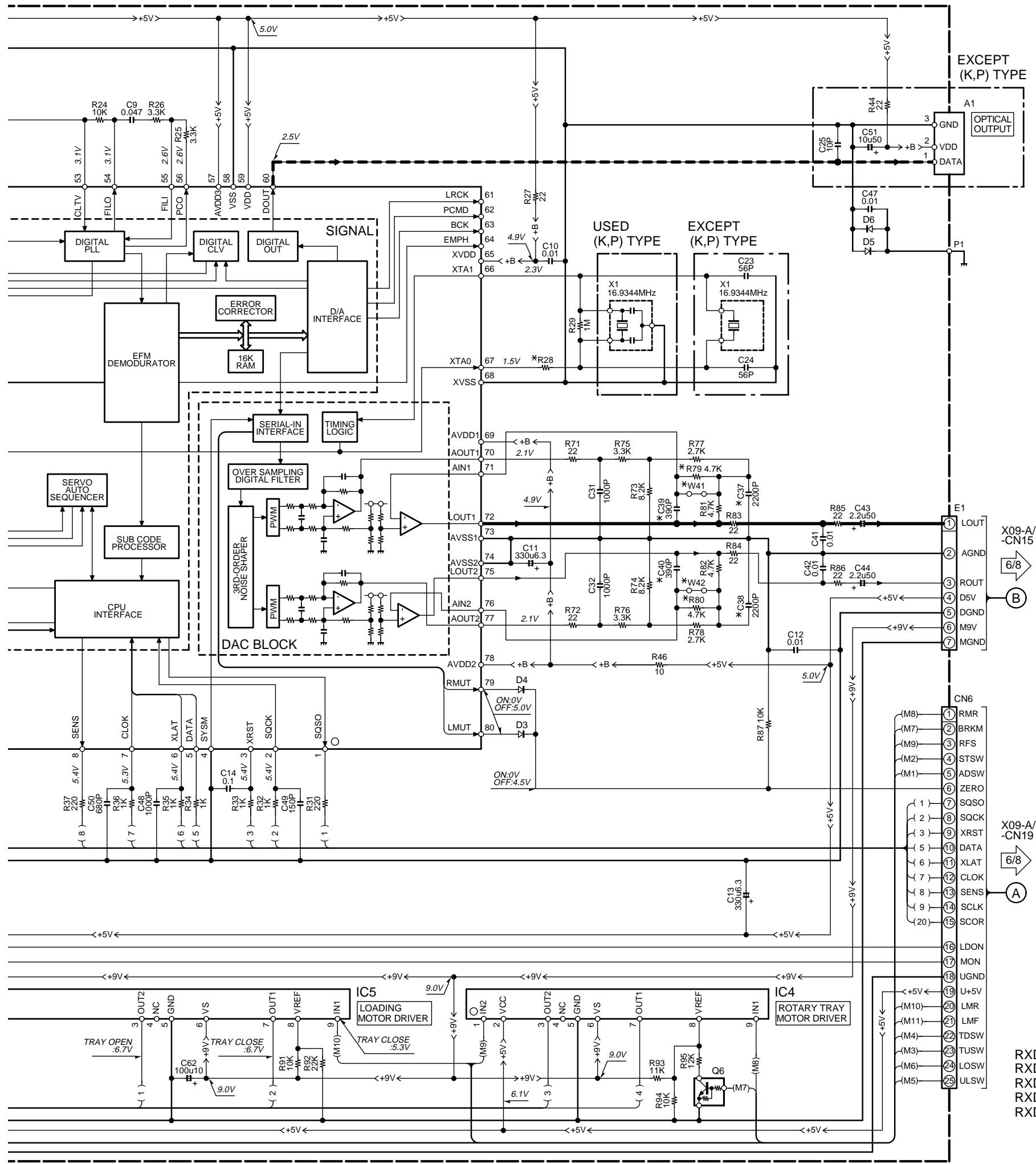
IC1 : CXA1571M
IC2 : CXD2587Q
IC3 : BA5979S
IC4,5 : TA8409S
Q1 : 2SA954(L,K)
Q6,7 : DTC124ESA or UN4212
Q8 : 2SB764(E,F)
D1-6 : 1SS133 or HSS104A
| DESTINATION | UNIT No. | C23,24,37-40 | R28 | R79,80 | W41,42 | |
| COUNTRY | ABB | |||||
| U.S.A. | K | 0-10 | NO | 390 | NO | YES |
| CANADA | P | |||||
| EXCEPT RXD-A5/A8 (X32-3592-71) | ||||||
| DESTINATION | UNIT No. | C23,24,37-40' | R28 | R79,80' | W41,42' | |
| COUNTRY | ABB. | |||||
| JAPAN | J | 2-71 | YES | 680 | YES | NO |
| PX | Y | |||||
| GENERAL MARKET | M | |||||
| AUSTRALIA | X | |||||
| U.K. | T | |||||
| EUROPE | E | |||||
| EUROPE | E2 | |||||
| RUSSIA | Q | |||||
CAUTION: For continued safety, replace safety critical components only with manufacturer's recommended parts (refer to parts list). indicates safety critical components. For continued protection against risk of fire, replace only with same type and rating fuse(s). To reduce the risk of electric shock, leakage-current or resistance measurements shall be carried out (exposed parts are acceptably insulated from the supply circuit) before the appliance is returned to the customer.
The DC voltage is an actual reading measured with a high impedance type voltmeter. The measurement value may vary depending on the measuring instruments used or on the product. Refer to the voltage during PLAY unless otherwise specified; The value shown in ( ) is the voltage measured at the moment of STOP.
RXD-A5/A8(K) (1/8)
RXD-501/501E/501W(E) (1/8)
RXD-551/551E/551W/571S(E) (1/8)
RXD-701/701E/701W(E) (1/8)
RXD-751/751E/751W/771S(E) (1/8)
and rating face(s). To reduce the risk of electric shock, leakage-current or resistance measurements shall be carried out (exposed parts are acceptably insulated from the supply circuit) before the appliance is returned to the customer.
The DC voltage is an actual reading measured with a high impedance type voltmeter with a cassette loaded at playback mode. The measurement value may vary depending on the measuring instruments used or on the product. Bias circuit DC voltage is measured while in the record mode.
DOLBY and the double-D symbol are trademarks of Dolby Laboratories Licensing Corporation. Noise reduction circuit made under license from Dolby Laboratories Licensing Corporation.
RXD-501/551/701/751 (X05-490X-XX)
| DESTINATION | UNIT No. | A | B | C39,59,79,88 | C48 | C53,54 | C55,56 | C67 | C68 | C77,78 | R3 | R16 | R43,44 | R57 | R60 | L62 | L63 | W51,52,54,55 | W61 | W68,74,79 | J2 | A1 | |
| COUNTRY | ABB. | ||||||||||||||||||||||
| U.K. | T | 0-51 | YES | NO | NO | 560P | 0.015 | 2.2u35 | 33P | NO | YES | 3.3K | 22 | 22K | NO | YES | L39-1368 | NO | NO | YES | NO | F10-1053 | W02-2640 |
| EUROPE | E | 2-70 | NO | YES | 22P | YES | NO | L39-1367 | YES | YES | |||||||||||||
RXD-501E/551E/701E/751E (X05-4902-70)
| DESTINATION | UNIT No. | A | B | C39,59,79,88 | C48 | C53,54 | C55,56 | C67 | C68,77,78 | R3 | R16 | R43,44 | R57,60 | L62 | L63 | W68,74,79 | W51,52,54,55,61 | J2 | A1 | |
| COUNTRY | ABB | |||||||||||||||||||
| EUROPE | E2 | 2-70 | NO | YES | NO | 560P | 0.015 | 2.2u35 | 22P | YES | 3.3K | 22 | 22K | NO | L39-1367 | YES | NO | YES | F10-1053 | W02-2640 |
RXD-501W/551W/701W/751W(X05-4903-81)
| DESTINATION COUNTRY | UNIT NO. | A | B | C39.59, 79.88 | C48 | C53, 54 | C55, 56 | C67 | C68, 77, 78 | R3 | R16 | R43, 44 | R57 | R60 | L62 | L63 | W68, 74, 79 | W51, 52, 54, 55, 61 | J2 | A1 | |
| PUSSIA | Q | 3-81 | YES | NO | YES | 470P | 0.018 | 3.3u25 | 22P | NO | 330 | 47 | 12K | YES | NO | L39-1368 | NO | YES | NO | F10-1088 | W02-2641 |
POLAR UNIT


Y39-2850-10
The DC voltage is an actual reading measured with a high impedance type voltmeter as the AM/FM signal generator is specified to the conditions as shown in the list below. The measurement value may vary depending on the measuring instruments used or on the product. The value shown in ( ) is actual reading measured in the AM made.
| MODE | CARRIER | MODULATION | ANT INPUT | |
| FREQUENCY | DEVIATION | |||
| FM | 98MHz | 1kHz | STEREO 67.5kHz 7.5kHz(Pilot) | 60dB |
| AM | 1000(999)kHz | 400Hz | MONO 30% MOD | 60dB |
CAUTION: For continued safety, replace safety critical components only with manufacturer's recommended parts (refer to parts list). indicates safety critical components. For continued protection against risk of fire, replace only with same type and rating fuse(s). To reduce the risk of electric shock, leakage-current or resistance measurements shall be carried out (exposed parts are acceptably insulated from the supply circuit) before the appliance is returned to the customer.
RED-501/551/701/751(T,E) (4/8)
RXD-501E/551E/701E/751E(E2) (4/8)
RXD-501W/551W/701W/751W(Q) (4/8)
(X05-4710-21) : RXD-571S/771S


2SC184
2301643
2SC2003
2SC2878
2002013
2SC3246
E C
SA
D.
SA
m = 311
6
C
m = 311 ;
65D
63D 70 67D D TG
65D-D TC74HC166AP
C
2SA1175
2SC2785
UN4212
TA8409S
BA3126N
KA1571M
NJU7313AL
BA5979S
A10393
2SA992
2CB764
ZSB764
2SC1845
2SC2003
23C2003
2SC2878
2SC3246
2303240


LA1836
DTA124ESA
DTG124ESA
DTCT24ESA
UN4112
2SC1740S
23617403
2SB1218A
06C2714
25C2714
2SC4081
2SD1810A
23D1819A
2SD2114K
IR3R42
NJM4565D
N.JM4565D-D
TC4052BP
TC74HC166AP
M4565D
M4565D-D

SAA6579/R
SAA6579
SK302

BA3126N
NJM2904M
TA78L012AF
LA1832
LC72131
2
M62430FP
LA1832
NJU7313AL
CXD2587Q
HA12209F
LA1837
BA5979S
CAUTION: For continued safety, replace safety critical components only with manufacturer's recommended parts (refer to parts list). indicates safety critical components. For continued protection against risk of fire, replace only with same type and rating fuse(s). To reduce the risk of electric shock, leakage-current or resistance measurements shall be carried out (exposed parts are acceptably insulated from the supply circuit) before the appliance is returned to the customer.
The DC voltage is an actual reading measured with a high impedance type voltmeter. The measurement value may vary depending on the measuring instruments used or on the product. Refer to the voltage during PLAY unless otherwise specified; The value shown in ( ) is the voltage measured at the moment of STOP.

IC21 PIN VOLTAGE
| MODELS | 1 | 2 | 3 | 4 | 5 | 6 | 7 | 8 | 9-11 | 12-15 | 16 | 17 | 18,19 | 20 | 21,22 | 23,24 | 25 | 26 |
| RXD-A5 RXD-501/551 | 54.3V | OV | 54.3V | OV | OV | OV | OV | -54.8V | -54.8V | OV | -53.0V | 53.0V | OV | -51.8V | OV | N/C | N/C | N/C |
| RXD-A8 RXD-701/751 | 64.3V | OV | 29.6V | 29.8V | 22.4V | -22.8V | -30.8V | -64.3V | -30.6V | OV | -60.7V | 60.5V | OV | -59.4V | OV | OV | -30.6V | OV |
| MODELS | A | B | C | D |
| RXD-A5 RXD-501/551 | 26.0V | -27.0V | 55.0V | -55.0V |
| RXD-A8 RXD-701/751 | 29.8V | -30.4V | 64.3V | -64.3V |
(X09-)(B/7) CN5 TERMINAL VOLTAGE
| MODELS | ① | ② | ③ | ④⑤ | ⑥ | ⑦ | ⑧ | ⑨ | ⑩ | ⑪⑫ | ⑭ |
| RXD-A5 RXD-501/551 | -27.0V | 24.3V | 26.0V | 12.2V | 10.5V | 12.4V | 0V | -54.0V | 0V | AC5.0V | 0V |
| RXD-A8 RXD-701/751 | -30.4V | 28.0V | 29.8V | 11.9V | 11.8V | 13.7V | 0V | -63.2V | 0V | AC5.4V | 0V |
WH7
(X09-600X-XX) (C/8): RXD-A5/RXD-501/RXD-501E/RXD-551E/RXD-501W/RXD-551W/RXD-551/RXD-571S
(X09-494X-XX) (C/8): RXD-A8/RXD-701/RXD-701E/RXD-751E/RXD-701W/RXD-751W/RXD-751/RXD-771S
- New Parts
Parts without Parts No. are not supplied.
Y: PX(Far East, Hawaii)
T:Europe
E:Europe
G:Germany
V:China(Shanghai)
Y:AAFES(Europe)
X: Australia
0: Russia
H:Korea
M:Other Areas
indicates safety critical components.
- New Parts
Parts without Parts No. are not supplied.
indicates safety critical components.
- New Parts
Parts without Parts No. are not supplied.
Y: PX(Far East, Hawaii)
T:Europe
E:Europe
G:Germany
V:China (Shanghai)
Y:AAFES(Europe)
X:Australia
0: Russia
H:Korea
M:Other Areas
indicates safety critical components.
- New Parts
Parts without Parts No. are not supplied.
Y: PX(Far East, Hawaii)
T:Europe
E:Europe
G:Germany
V:China (Shanghai)
Y:AAFES(Europe)
X: Australia
Q: Russia
H:Korea
M:Other Areas
indicates safety critical components.
- New Parts
Parts without Parts No. are not supplied
indicates safety critical components.
- New Parts
Parts without Parts No. are not supplied.
Y: PX(Far East, Hawaii)
T:Europe
E:Europe
G:G
many V:China (Shanghai)
Y:AAFES(Europe)
X: Australia
0: Russia
H:Korea
M:Other Areas
indicates safety critical components.
- New Parts
Parts without Parts No. are not supplied.
Y: PX(Far East, Hawaii)
T: Europe
E:Europe
G:Germany
V:China (Shanghai)
Y:AAFES(Europe)
X: Australia
Q: Russia
H:Korea
M:Other Areas
indicates safety critical components
- New Parts
Parts without Parts No. are not supplied.
indicates safety critical components.
- New Parts
Parts without Parts No. are not supplied.
Y: PX(Far East, Hawaii)
T:Europe
E:Europe
G:Germany
V: China (Shanghai)
Y:AAFES(Europe)
X: Australia
2: Russia
H:Korea
M:Other Areas
indicates safety critical components.
- New Parts
Parts without Parts No. are not supplied
indicates safety critical components.
- New Parts
Parts without Parts No. are not supplied.
Y: PX(Far East, Hawaii)
T: Europe
E:Europe
G:Germany
V: China (Shanghai)
Y:AAFES(Europe)
X: Australia
Q: Russia
H:Korea
M:Other Areas
indicates safety critical components.
- New Parts
Parts without Parts No. are not supplied.
Y: PX(Far East, Hawaii)
T: Europe
E:Europe
G:Germar
V: China (Shanghai)
Y:AAFES(Europe)
X: Australia
Q: Russia
H:Korea
M:Other Areas
indicates safety critical components.
- New Parts
Parts without Parts No. are not supplied.
Y: PX(Far East, Hawaii)
T:Europe
E:Europe
any
V:China (Shanghai)
Y:AAFES(Europe)
X: Australia
0: Russia
a
M:Other Areas
indicates safety critical components.
- New Parts
Parts without Parts No. are not supplied.
indicates safety critical components.
- New Parts
Parts without Parts No. are not supplied.
Y: PX(Far East, Hawaii)
T: Europe
E:Europe
G:Germany
V: China (Shanghai)
Y:AAFES(Europe)
X: Australia
0: Russia
H:Korea
M:Other Areas
indicates safety critical components.
- New Parts
Parts without Parts No. are not supplied.
Y: PX(Far East, Hawaii)
T:Europe
E:Europe
G:Germany
V:China (Shanghai)
Y:AAFES(Europe)
X: Australia
: Russia
H:Korea
M:Other Areas
indicates safety critical components.
- New Parts
Parts without Parts No. are not supplied
Y: PX(Far East, Hawaii)
Y:AAFES(Europe)
K:USA
T:Europe
X: Australia
P:Canada
E:Europe
Q: Russia
R:Mexico
G:Germany
H:Korea
C:China
V:China(Shanghai)
M:Other Areas
I:Malaysia
indicates safety critical components.
- New Parts
Parts without Parts No. are not supplied.
Y: PX(Far East, Hawaii)
T: Europe
E:Europe
G:German
V:China(Shanghai)
Y:AAFES(Europe)
X: Australia
Q: Russia
H:Korea
M:Other Areas
indicates safety critical components.
- New Parts
Parts without Parts No. are not supplied.
indicates safety critical components.
- New Parts
Parts without Parts No. are not supplied.
Y:AAFES(Europe) X:Austra
Asia H:Korea M:Other Areas
indicates safety critical components.
- New Parts
Parts without Parts No. are not supplied.
indicates safety critical components.
- New Parts
Parts without Parts No. are not supplied.
G:Germany V:China (Shanghai)
RXD-501/501E/501W/551/551E/551W/571S/A5
Y:AAFES(Europe) X:Austra
Q: Russia
ea M:Other Areas
7:RXD-701/701E/701W/751/751E/751W/771S/A8
indicates safety critical components.
- New Parts
Parts without Parts No. are not supplied.
Y: PX(Far East, Hawaii)
Y:AAFES(Europe)
K:USA
T: Europe
X: Australia
P: Canada
E:Europe
0: Russia
R:Mexico
G:Germany
H:Korea
C:China
V: China (Shanghai)
M:Other Areas
I:Malaysia
indicates safety critical components.
- New Parts
Parts without Parts No. are not supplied.
indicates safety critical components.
- New Parts
Parts without Parts No. are not supplied
Y: PX(Far East, Hawaii)
Y:AAFES(Europe)
K:USA
T:Europe
X:Australia
P:Canada
E:Europe
Q: Russia
R:Mexico
G:Germany
H:Korea
C:China
V:Ch
M:Other Areas
I:Malaysia
indicates safety critical components.
- New Parts
Parts without Parts No. are not supplied
Y: PX(Far East, Hawaii)
T: Europe
E:Europe
G:Germany V:China (Shanghai)
Y:AAFES(Europe)
X:Australia
Q: Russia
H:Korea
M:Other Areas
indicates safety critical components.
- New Parts
Parts without Parts No. are not supplied.
Y: PX(Far East, Hawaii)
T:Europe
E:Europe
G:Germany
V:China (Shanghai)
Y:AAFES(Europe)
X:Australia
Q: Russia
H:Korea
M:Other Areas
indicates safety critical components.
- New Parts
Parts without Parts No. are not supplied.
Y: PX(Far East, Hawaii)
T:Europe
E:Europe
G:Germany
V: China (Shanghai)
Y:AAFES(Europe)
X:Australia
Q: Russia
H:Korea
M:Other Areas
indicates safety critical components.
HOW TO READ THE PARTS LIST
ABBREVIATION OF MODEL AND MASS PRODUCTION'S DESTINATIONS
| MODEL | ABB. | Australia | Canada | China | England | Europe | Germany | Korea | Malaysia |
| RXD-501 | 5 | X | - | - | T | E | - | - | - |
| RXD-501W | - | - | - | - | - | - | - | - | |
| RXD-501E | - | - | - | - | E2 | - | - | - | |
| RXD-551 | X | - | - | T | E | - | - | - | |
| RXD-551W | - | - | - | - | - | - | - | - | |
| RXD-551E | - | - | - | - | E2 | - | - | - | |
| RXD-571S | - | - | - | - | - | - | - | - | |
| RXD-A5 | - | P | - | - | - | - | - | - | |
| RXD-701 | 7 | X | - | - | T | E | - | - | - |
| RXD-701W | - | - | - | - | - | - | - | - | |
| RXD-701E | - | - | - | - | E2 | - | - | - | |
| RXD-751 | X | - | - | T | E | - | - | - | |
| RXD-751W | - | - | - | - | - | - | - | - | |
| RXD-751E | - | - | - | - | E2 | - | - | - | |
| RXD-771S | - | - | - | - | - | - | - | - | |
| RXD-A8 | - | P | - | - | - | - | - | - | |
| MODEL | ABB. | Mexico | PX/AAFES | Russia | Scandinavia | Shanghai | USA | Other area | |
| RXD-501 | 5 | - | - | - | - | - | - | - | - |
| RXD-501W | - | - | Q | - | - | - | - | - | |
| RXD-501E | - | - | - | - | - | - | - | - | |
| RXD-551 | - | Y | - | - | - | - | M | - | |
| RXD-551W | - | - | Q | - | - | - | - | - | |
| RXD-551E | - | - | - | - | - | - | - | - | |
| RXD-571S | - | - | - | - | - | - | M2 | - | |
| RXD-A5 | - | - | - | - | - | K | - | - | |
| RXD-701 | 7 | - | - | - | - | - | - | - | - |
| RXD-701W | - | - | Q | - | - | - | - | - | |
| RXD-701E | - | - | - | - | - | - | - | - | |
| RXD-751 | - | Y | - | - | - | - | M | - | |
| RXD-751W | - | - | Q | - | - | - | - | - | |
| RXD-751E | - | - | - | - | - | - | - | - | |
| RXD-771S | - | - | - | - | - | - | M2 | - | |
| RXD-A8 | - | - | - | - | - | K | - | - |
SPECIFICATIONS
Main unit
[Amplifier section]
(RXD-A8/RXD-7...Series)
Rated power output (U.S.A. and Canada)
100 watts per channel minimum RMS, both channels driven, at 6 from 40Hz to 14kHz with no more than 0.9% total harmonic distortion.
Effective output power during STEREO operation
U.S.A. and Canada
FRONT (1 kHz, 0.9% T.H.D., 6Ω) 100 W + 100 W
Subwoofer (60 Hz, 0.9% T.H.D., 12Ω // 12Ω) ..... 100 W
Other countries
FRONT (1 kHz, 10% T.H.D.,6 Ω) 135 W + 135 W
Subwoofer (60 Hz, 10% T.H.D., 12Ω // 12Ω) 135 W
Rated output power during STEREO operation
Europe, U.K. and Russia
(DIN)1 kHz, 0.7 % T.H.D.,6 Ω, 100 W + 100 W
Other countries
1 kHz, 1.0% T.H.D., 6Ω, 115 W + 115 W
(RXD-A5/RXD-5...Series)
Rated power output (U.S.A. and Canada)
70 watts per channel minimum RMS, both channels driven, at 6 from 40Hz to 14kHz with no more than 0.9% total harmonic distortion.
Effective output power during STEREO operation
1 kHz, 10% T.H.D.,6Ω, 100 W + 100 W
Rated output power during STEREO operation
Europe, U.K. and Russia
(DIN)1 kHz, 0.7% T.H.D.,6Ω, .80 W + 80 W
Other countries
1 kHz, 1.0% T.H.D., 6Ω, 95 W + 95 W
Signal to noise ratio
AUX 90 dB
Input sensitivity / impedance
AUX. 400 mV / 47kΩ
MIC 1, 2 (Except for some arears) 2.5 mV / 22 k
Output level / impedance
AUX (Except for U.S.A. and Canada) 0.5 V / 3.3 kΩ
(RXD-A5/RXD-5...Series)
SUPER WOOFER PREOUT 1.8 V/3.3 kΩ
[Tuner section]
FM tuner section
Tuning frequency range. 87.5 MHz 108 MHz
(For Russia) 65.0 MHz ~74.0 MHz
MW (AM) tuner section
Tuning frequency range
Europe, U.K. and Russia 531 kHz 1,602 kHz
Other countries
9kHz step 531 kHz ~ 1,602 kHz
10kHz step 530 kHz 1,610 kHz
U.S.A. and Canada 530 kHz ~ 1,700 kHz
LW tuner section (For the United Kingdom and Russia)
Tuning frequency range. 153 kHz ~ 279 kHz
SW tuning section (RXD-771S/RXD-571S)
Tuning frequency range. 5.9MHz 17.9MHz
[Csette deck section]
Track 4-track,2-channel stereo
Recording system AC bias system
(Frequency: 105 kHz)
Heads
A deck Playback head 1
B deck Playback / recording head 1
Erasing head 1
Motors 2
Fast winding time Approx. 115 seconds
(C-60 tape)
[CD player section]
Laser Semiconductor laser
Wow & flutter ....Less than unmeasurable limit
(Except for U.S.A. and Canada)
Digital output (Optical) -15 dBm -21 dBm
(Wave length 660 nm)
[General]
Power consumption. (RXD-7...Series) 210 W
(RXD-A8/RXD-A5/RXD-5...Series) 200 W
Dimensions W:280 mm (11")
H:332 mm (13-1/16")
D:344mm(13-9/16")
Weight (net) .........(RXD-A8/RXD-7...Series) 11.1 kg (24.5 lb)
(RXD-A5/RXD-5...Series) 10.5 kg (23.1 lb)

-
KENWOOD follows a policy of continuous advancements in development. For this reason specifications may be changed without notice.
-
The full performance may not be exhibited in extremely could location (under a water-freezing temperature).
Note:
Component and circuit are subject to modification to insure best operation under differing local conditions. This manual is based on Europe (E) standard, and provides information on regional circuit modification through use of alternate schematic diagrams, and information on regional component variations through use of parts list.
KENWOOD CORPORATION
14-6,Dogenzaka 1-chome, Shibuya-ku, Tokyo, 150-8501 Japan
KENWOOD SERVICE CORPORATION
P.O BOX 22745, 2201 East Dominguez St., Long Beach, CA 90801-5745, U.S.A.
KENWOOD ELECTRONICS CANADA INC.
6070 Kestrel Road, Mississauga, Ontario, Canada L5T 1S8
KENWOOD ELECTRONICS LATIN AMERICA S.A.
P.O BOX 55-2791, Piso 6 plaza Chase, Cl. 47 y Aquilino de la Guardia Panama, Republic de Panama
KENWOOD ELECTRONICS BRASIL LTDA.
Av Indianópolis, 628, 04062-001 Planalto Paullsta São Paulo-SP-Brasil
KENWOOD ELECTRONICS U.K. LIMITED
KENWOOD House, Dwight Road, Watford, Herts., WD1 8EB., United Kingdom
KENWOOD ELECTRONICS BELGUM N.V.
Meachelsestenweg 418, B-1930 Zaventem, Belgium
KENWOOD ELECTRONICS DEUTSCHLAND GMBH
Rembrucker Str. 15, 63150 Heusenstamm, Germany
KENWOOD ELECTRONICS FRANCE S.A.
13 Boulevard Ney, 75018 Paris, France
Via G. Sirtori, 7/9 20129, Milano, Italy
KENWOOD IBÉRICA S.A.
Bolivia, 239-08020 Barcelona, Spain
KENWOOD ELECTRONICS AUSTRALIA PTY. LTD.
(A.C.N. 001499 074)
P.O Box 504, 8 Figtree Drive, Australia Centre, Homebush, N.S.W. 2140, Australia
KENWOOD & LEE ELECTRONICS, LTD.
Unit 3712-3724, Level 37, Tower 1, Metroplaza, 223 Hing Fong Road, Kwai Fong N.T., Hong Kong
KENWOOD ELECTRONICS GULF FZE
P.O.Box 61318, Jebel Ali, Dubai, U.A.E.
KENWOOD ELECTRONICS SINGAPORE PTE LTD.
No. 1 Genting Lane #02-02, KENWOOD Building, Singapore, 349544
KENWOOD ELECTRONICS (MALAYSIA) SDN BHD.
4.01 Level 4, Wisma Academy Lot 4A, Jalan 19/1 46300 Petaling Jaya Selangor Darul Ehsan Malaysia
KENWOOD ELECTRONICS (THAILAND) CO., LTD.
573/111 Soi Ramkhamaeng 39, Ramkhamaeng Road, Wangthongliang, Bangkok, Bankok 10301 Thailand