MIC2111A - Electronic controller Microchip - Free user manual and instructions
Find the device manual for free MIC2111A Microchip in PDF.

User questions about MIC2111A Microchip
0 question about this device. Answer the ones you know or ask your own.
Ask a new question about this device
Download the instructions for your Electronic controller in PDF format for free! Find your manual MIC2111A - Microchip and take your electronic device back in hand. On this page are published all the documents necessary for the use of your device. MIC2111A by Microchip.
USER MANUAL MIC2111A Microchip
The MIC2111B is a programmable-frequency, valley-current/voltage-mode PWM controller that provides the control and protection features necessary for power devices and drivers that use current-sensing across the inductor. The MIC2111B provides a single tri-state PWM logic signal to DrMOS modules to realize low output voltage, high current power supply. The device has precision enable and power good (PG) functions for the sequencing of multiple power supplies. In addition, the solution is compatible with intelligent power stages in a high-current, step-down DC/DC converter.
The MIC2111B evaluation board operates over an input supply range of 5.5V to 16V and provides a regulated output at up to 20A of load current. The output voltage is adjustable down to 0.6V with a typical accuracy of ±1%. The evaluation board operates at a switching frequency of 500kHz, in valley current mode.
The MIC2111B utilizes a programmable control architecture. The MIC2111B evaluation board is configured for valley current mode control. An undervoltage lockout feature is provided to ensure proper operation under power sag conditions. An adjustable soft-start feature is provided to reduce inrush current. An adjustable current-limit is provided. "Hiccup" mode short-circuit protection and thermal shutdown ensures protection of the IC during fault conditions.
The basic parameters of the evaluation board are:
• V IN supply: 5.5V to 16V
• Output: 1.2V at 20A
- 500kHz switching frequency (Adjustable from 200kHz to 2MHz)
- Control mode: Valley current mode (Adjustable to voltage mode)
The customer can configure the MIC2111B evaluation board to operate in voltage mode through the following jumper selections.
| Control Mode P1 | P2 | |
| Valley Current Mode | Pins 1-2 Pins 1-2 | |
| Voltage Mode Pins | 2-3 OPEN | |
For information about compensation component selection, see the MIC2111 datasheet on Micrel's website at: www.micrel.com.
Requirements
The MIC2111B evaluation board requires only a single power supply with at least 10A current capability. The MIC2111B has an on-board 5V LDO to power the internal biasing of the MIC2111B IC and DrMOS gate drive supply.
Power-up Precautions
The evaluation board does not have reverse polarity protection. Applying a negative voltage to the VIN terminal may damage the device. In addition, the maximum V_IN operating voltage of the MIC2111B evaluation board is 16V.
Ordering Information
| Part Number Description | |
| MIC2111BYMT | MIC2111B Evaluation Board |
Getting Started
1. Connect a supply to the VIN and GND terminals.
Pay careful attention to the polarity and the supply range (5.5V < V_IN < 16V). An ammeter may be placed between the input supply and the VIN terminal to the evaluation board. Ensure that the supply voltage is monitored at the VIN terminal. The ammeter and/or power lead resistance can reduce the voltage supplied to the input. Do not apply power until Step 4.
2. Connect the load to the VOUT and ground terminals.
The load can be either passive (resistive) or active (as in an electronic load). An ammeter can be placed between the load and the VOUT terminal. Ensure that the output voltage is monitored at the VOUT terminal.
3. Enable input.
An EN connector is provided on the evaluation board for users to easily access the enable feature. The output of the MIC2111B turns on when V_cc exceeds the UVLO threshold. The output of the MIC2111B evaluation board may be turned off by shorting the EN pin to ground.
4. Turn on the power.
Turn on the VIN power supply and verify that the output voltage is regulated to 1.2V.
Evaluation Board Description
Output Voltage
The output voltage on the MIC2111B evaluation board is adjustable. It is set by adjusting the feedback resistors and using the following equation.
$$ V O U T = V F B x \left(1 + \frac {R 1 4}{R 1 1}\right) \text { Eq. } 1 $$
where V_FB = 0.6V and R11 is 4.99kΩ for a 1.2V output voltage. Leaving R11 open gives a 0.6V output voltage. The output can be adjusted from 0.6V to 3.46V by changing the value of R11 according to the equation above.
The output voltage should not be set in excess of 3.46V due to the need for headroom for the current sense amplifier of MIC2111B. Please refer to the Application Information section of the MIC2111 datasheet for setting the output voltage.
Oscillator Frequency
The MIC2111 has an internal oscillator by which the frequency can be set through an external resistor at the FREQ pin. The switching frequency can be programmed from 200kHz to 2MHz by using the following equation.
$$ R _ {F R E Q} = \frac {1 0 ^ {1 1}}{F _ {S W [ \Omega ]}} \quad \text { Eq.2 } $$
where F_sw = the desired switching frequency in Hz.
The MIC2111 has digital soft-start/soft-stop (SS) to avoid high inrush current in the input supply lines. The soft-start time can be programmed with an external resistor connected from the SS pin to GND. Table 1 illustrates resistor values and soft-start times. Soft-stop time is the same as the programmed soft-start time (contact the factory for instructions on disabling soft-stop).
Table 1. Soft-Start Programming
| E96 Range Resistance | Soft-Start |
| 6.19kΩ 64μs | |
| 19.1kΩ 128μs | |
| 30.9kΩ 256μs | |
| 44.2kΩ 512μs | |
| 56.2kΩ 768μs | |
| 68.1kΩ 1024μs | |
| 80.6kΩ 1536μs | |
| 93.1kΩ 2048μs | |
| 105kΩ 3072μs | |
| 118kΩ 4096μs | |
| 130kΩ 6144μs | |
| 143kΩ 8192μs | |
| 154kΩ 16384μs | |
| 169kΩ 24576μs | |
| 182kΩ 32768μs | |
| Open | 2048μs |
Evaluation Board Performance
line
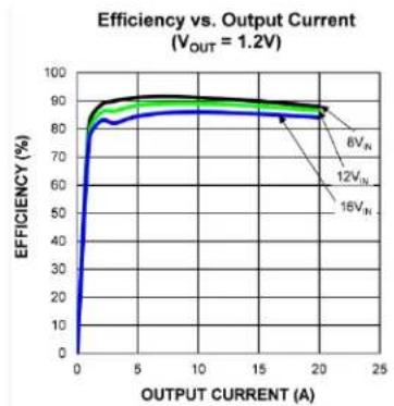
| OUTPUT CURRENT (A) | EFFICIENCY (%) | | ------------------ | -------------- | | 0 | 0 | | 5 | 85 | | 10 | 88 | | 15 | 87 | | 20 | 85 | | 25 | 83 |
line
| OUTPUT CURRENT (A) | EFFICIENCY (%) | | ------------------ | -------------- | | 0 | 0 | | 5 | 85 | | 10 | 90 | | 15 | 88 | | 20 | 85 | | 25 | 80 |
line
| SWITCHING FREQUENCY (MHz) | VDD SUPPLY CURRENT (mA) | | ------------------------- | ----------------------- | | 0.5 | 28 | | 1 | 45 | | 1.5 | 58 | | 2 | 68 |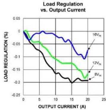
line
| OUTPUT CURRENT (A) | 8V_IN | 12V_IN | 16V_IN | | ------------------ | ----- | ------ | ------ | | 0 | 0.0 | 0.0 | 0.0 | | 5 | -0.05 | -0.03 | -0.02 | | 10 | -0.15 | -0.08 | -0.05 | | 15 | -0.2 | -0.12 | -0.1 | | 20 | -0.2 | -0.18 | -0.15 | | 25 | -0.2 | -0.2 | -0.2 |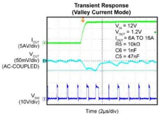
line
| Parameter | Value | | --------- | --------- | | V_IN | 12V | | V_OUT | 1.2V | | I_CUT | 6A | | R5 | 10kΩ | | C6 | 1nF | | C5 | 47nF | | V_IN | 12V | | V_OUT | 1.2V | | I_CUT | 6A | | R5 | 10kΩ | | C6 | 1nF | | C5 | 47nF | | V_IN | 12V | | V_OUT | 1.2V | | I_CUT | - | | R5 | - | | C6 | - | | C5 | - | | V_IN | 12V | | V_OUT | 1.2V | | I_CUT | - | | R5 | - | | C6 | - | | C5 | - | | V_IN | 12V | | V_OUT | 1.2V | | I_CUT | - | | R5 | - | | C5 | - | | C5 | - |
line
| Time (20μs/div) | I_OUT (5AV/div) | V_OUT (50mV/div) | V_SW (10V/div) | | --------------- | --------------- | ---------------- | -------------- | | 0 | 12V | 1.2V | 47nF | | 6A | 6A | TO 6A | - | | 16A | - | - | - | | 20A | - | - | - |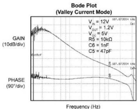
line
| Parameter | Value | | --------- | --------- | | VIN | 12V | | VOUT | 1.2V | | VCO | 5V | | R5 | 10kΩ | | C6 | 1nF | | C5 | 47pF |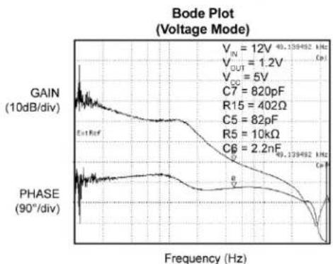
line
| Frequency (Hz) | GAIN (10dB/div) | PHASE (90°/div) | | -------------- | --------------- | ---------------- | | 40.139492 | 40.139492 | 40.139492 |Evaluation Board Schematic

text_image
U3 MICS209-5.0Y5 C4 1μF IN GND OUT 3 2 5V PGND R21 147kΩ EN R20 1kΩ C22 1nF SGND EN SLO PE U1 MIC2111YML OVP PG RS+ RS- VDIF FB COMP SEL AGND AGND P1 3 2 1 2 3 12 6 5 8 R30 10kΩ C6 1nF R29 10kΩ T7 C17 open R25 200kΩ R27 118kΩ C23 Open R28 188kΩ R16 Open SGND R30 10pF C24 10pF C21 10pF C23 10pF R27 118kΩ R28 188kΩ R16 Open SGND R30 10kΩ T7 C24 10pF C21 10pF C24 10pF C23 10pF R30 10kΩ T7 C24 10pF C21 10pF C24 10pF C23 10pF R30 10kΩ T7 C24 10pF C21 10pF C24 10pF C23 10pF R32 1.21D C32 1μF SGND R4 10kΩ R7 10kΩ SV 5V SGND R8 1.31D C4 1μF SGND DH DL 9 DHL DL 9 DHL DL 9 DHL DL 9 DHL DL 9 DHL DL 9 DHL DL 9 DHL DL 9 DHL DL 9 DHL DL 9 DHL DL 9 DHL DL 9 DHL DL 9 DHL DL 9 DHL DL 9 DHL DHL 9 DHL DL 9 DHL DL 9 DHLBill of Materials
| Item | Part Number | Manufacturer | Description | Qty. |
| C1 | C1608X7R1C684K080AC | TDK^(1) | 0.68μF Ceramic Capacitor, X7R, 0603 Size, 16V | 1 |
| C2, C21, C24, C30 | C1608C0G1H100D | TDK | 10pF Ceramic Capacitor, COG, 0603 Size, 50V | 4 |
| C3, C7, C16, C17, C23,C31, R2, R6, R13, R15, R16, R17, R22, R26 | OPEN | |||
| C4, C9, C18, C19, C27,C32,C33,C34 | C1608X5R1E105K | TDK | 1μF Ceramic Capacitor, X5R, 0603 Size, 25V | 6 |
| C5 | C1608C0G1H820J | TDK | 82pF Ceramic Capacitor, COG, 0603 Size, 50V | 1 |
| C6, C22 | C1608C0G1H102J | TDK | 1nF Ceramic Capacitor, COG, 0603 Size, 50V | 2 |
| C8, C10 | C3225X5R0J226M/1.60 | TDK | 22μF Ceramic Capacitor, X5R, 1210 Size, 6.3V | 2 |
| C11, C13 | C3225X5R0J107M | TDK | 100μF Ceramic Capacitor, X5R, 1210 Size, 6.3V | 2 |
| C12, C20 | C1608X7R1E104K | TDK | 100nF Ceramic Capacitor, X7R, 0603 Size, 25V | 2 |
| C15 | 6SVP470MX | Panasonic^(2) | 470μF OS-CON Capacitor, 6.3V | 1 |
| C25, C28, C29 | C3225X5R1E106M | TDK | 10μF Ceramic Capacitor, X5R, 1210 Size, 25V | 2 |
| C26 | EEEFP1E471AP | Panasonic | 470μF Alluminium Capacitor, 25V | 1 |
| L1 | 744325040 | Wurth Electric ^(3) | 0.4μH inductor, 37A saturation current | 1 |
| R1, R2, R3, R10 | CRCW060310R0FKEA | Vishay Dale ^(4) | 10Ω Resistor,0603 Size, 1% | 4 |
| R4, R5, R7, R9, R29, R30 | CRCW060310K0FKEA | Vishay Dale | 10kΩ Resistor,0603 Size, 1% | 4 |
| R8 | CRCW0603866RFKEA | Vishay Dale | 866Ω Resistor,0603 Size, 1% | 1 |
| R11, R14 | CRCW06034K99FKEA | Vishay Dale | 4.99kΩ Resistor,0603 Size, 1% | 2 |
| R11, R14 | CRCW06034K99FKEA | Vishay Dale | 4.99kΩ Resistor,0603 Size, 1% | 2 |
| R12, R31, RSW | CRCW06030000Z0EA | Vishay Dale | 0Ω Resistor,0603 Size, 1% | 3 |
| R18, R23 | CRCW06031R21FKEA | Vishay Dale | 1.21Ω Resistor,0603 Size, 1% | 2 |
| R19 | CRCW060311K0FKEA | Vishay Dale | 11kΩ Resistor,0603 Size, 1% | 1 |
| R20 | CRCW06031K00FKEA | Vishay Dale | 1kΩ Resistor,0603 Size, 1% | 1 |
| R21 | CRCW0603147KFKEA | Vishay Dale | 147kΩ Resistor,0603 Size, 1% | 1 |
| R24 | CRCW06035K49FKEA | Vishay Dale | 5.5kΩ Resistor,0603 Size, 1% | 1 |
| R25 | CRCW0603200KFKEA | Vishay Dale | 200kΩ Resistor,0603 Size, 1% | 1 |
| R27 | CRCW0603118KFKEA | Vishay Dale | 118kΩ Resistor,0603 Size, 1% | 1 |
| R28 | CRCW0603188KFKEA | Vishay Dale | 188kΩ Resistor,0603 Size, 1% | 1 |
| U1 | MIC2111B | Micrel, Inc. ^(5) | High-Performance, Multi-Mode, Step-Down Controller | 1 |
| U2 | SiC780ACD | Vishay | Integrated DrMOS power stage | 1 |
| U3 | MIC5209-5.0YS | Micrel, Inc. | 500mA Low Noise LDO Regulator | 1 |
Notes:
1. TDK: www.tdk.com.
2. Panasonic: www.industrial.panasonic.com.
3. Wurth Electronic: www.we-online.com.
4. Vishay Dale: www.vishay.com.
5. Micrel, Inc.: www.micrel.com.
PCB Layout Recommendations

text_image
MIC2111B EV BOARD SGND EN TJ DH DL 5V FLT GL SGND PGND P1 SGND PGND PG00D GH 2822.421 (mil) 1) Top Layer 1587.6 (mil)Top Layer
text_image
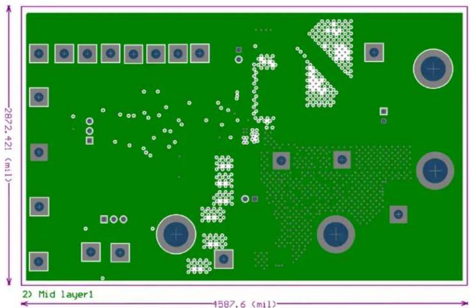
2822.421 (mil) 2) Mid layer1 4587.6 (mil)Mid Layer 1
PCB Layout Recommendations (Continued)

text_image
2872.421 (mil) 3)Mid layer 2 1587.6 (mil)Mid Layer 2

text_image
2872.421 (mil) 4) Bottom layer 4587.6 (mil)Bottom Layer
MICREL, INC. 2180 FORTUNE DRIVE SAN JOSE, CA 95131 USA
TEL +1 (408) 944-0800 FAX +1 (408) 474-1000 WEB http://www.micrel.com
Micrel, Inc. is a leading global manufacturer of IC solutions for the worldwide high-performance linear and power, LAN, and timing & communications markets. The Company's products include advanced mixed-signal, analog & power semiconductors; high-performance communication, clock management, MEMs-based clock oscillators & crystal-less clock generators, Ethernet switches, and physical layer transceiver ICs. Company customers include leading manufacturers of enterprise, consumer, industrial, mobile, telecommunications, automotive, and computer products. Corporation headquarters and state-of-the-art wafer fabrication facilities are located in San Jose, CA, with regional sales and support offices and advanced technology design centers situated throughout the Americas, Europe, and Asia. Additionally, the Company maintains an extensive network of distributors and reps worldwide.
Micrel makes no representations or warranties with respect to the accuracy or completeness of the information furnished in this datasheet. This information is not intended as a warranty and Micrel does not assume responsibility for its use. Micrel reserves the right to change circuitry, specifications and descriptions at any time without notice. No license, whether express, implied, arising by estoppel or otherwise, to any intellectual property rights is granted by this document. Except as provided in Micrel's terms and conditions of sale for such products, Micrel assumes no liability whatsoever, and Micrel disclaims any express or implied warranty relating to the sale and/or use of Micrel products including liability or warranties relating to fitness for a particular purpose, merchantability, or infringement of any patent, copyright, or other intellectual property right.
Micrel Products are not designed or authorized for use as components in life support appliances, devices or systems where malfunction of a product can reasonably be expected to result in personal injury. Life support devices or systems are devices or systems that (a) are intended for surgical implant into the body or (b) support or sustain life, and whose failure to perform can be reasonably expected to result in a significant injury to the user. A Purchaser's use or sale of Micrel Products for use in life support appliances, devices or systems is a Purchaser's own risk and Purchaser agrees to fully indemnify Micrel for any damages resulting from such use or sale.
© 2015 Micrel, Incorporated.