MIC2127 - Electronic controller Microchip - Free user manual and instructions
Find the device manual for free MIC2127 Microchip in PDF.

User questions about MIC2127 Microchip
0 question about this device. Answer the ones you know or ask your own.
Ask a new question about this device
Download the instructions for your Electronic controller in PDF format for free! Find your manual MIC2127 - Microchip and take your electronic device back in hand. On this page are published all the documents necessary for the use of your device. MIC2127 by Microchip.
USER MANUAL MIC2127 Microchip
75V, Synchronous Buck Controller Featuring Adaptive On-Time Control
Features
• Hyper Speed Control ^® Architecture Enables:
- High input to output voltage conversion ratio capability
- Any Capacitor™ stable
-
Ultra-fast load transient response
-
Wide 4.5V-75V Input Voltage Range
- Adjustable Output Voltage from 0.6V to 30V
• 270 kHz-800 kHz Programmable Switching Frequency
• Built-In 5V Regulator for Single-Supply Operation
• Auxiliary Bootstrap LDO for Improving System Efficiency - Internal Bootstrap Diode
- Selectable Light Load Operating Mode
- Enable Input and Power Good Output
• Programmable Current Limit
• Hiccup Mode Short-Circuit Protection - Soft Start, Internal Compensation and Thermal Shutdown
• Supports Safe Start-Up into a Prebiased Output
• AEC-Q100 Qualified (VAO suffix)
Applications
• Networking/Telecom Equipment
- Base Station, Servers
• Distributed Power Systems
• Industrial Power Supplies
• Automotive Power Supplies
Typical Application Circuit

text_image
MIC2127A 4.7 µF 10Ω 4.7 µF PG EN VCC MOOE VCC 100 kΩ 80 kΩ Freq Amo Rosc VOUT 0.1 µF DII BSI SW INR 1.3 kΩ DL FD EXTVDD 1 µF VOUT Q1 0.1 µF Q2 36 kΩ L1 10 µF Q1, Q2: SIR676/ADP L1: SRP*265A-130M, Bours C1: 165VP300M *Output voltage follows input voltage when the input is below the terap output voltage. 4.5V to 75V 2.2 µFX3 VCC C1 330 µF 47 µF VCC 5V@SAGeneral Description
The MIC2127A device is a constant-frequency synchronous buck controller featuring a unique adaptive on-time control architecture. The MIC2127A device operates over an input voltage range from 4.5V-75V. The output voltage is adjustable down to 0.6V with an accuracy of ±1%. The device operates with programmable switching frequency from 270 kHz to 800 kHz.
The MIC2127A device features a MODE pin that allows the user to select either Continuous Conduction mode or HyperLight Load® (HLL) mode under light loads. An auxiliary bootstrap LDO improves the system efficiency by supplying the MIC2127A internal circuit bias power and gate drivers from the output of the converter. A logic level enable (EN) signal can be used to enable or disable the controller. MIC2127A can start-up monotonically into a prebiased output. The MIC2127A device features an open drain power good signal (PG) that signals when the output is in regulation and can be used for simple power supply sequencing.
MIC2127A offers a full suite of protection features to ensure protection of the IC during Fault conditions. These include undervoltage lockout to ensure proper operation under power-sag conditions, "hiccup" mode short-circuit protection, internal soft start of 5 ms to reduce inrush current during start-up and thermal shutdown.
The MIC2127A device is available in a 16-pin 3 mm × 3 mm VQFN package, with an operating junction temperature range from -40°C to +125°C.
Package Type
MIC2127A
3×3VQFN*
(Top View)

text_image
V_IN V_DD A_GND FB 16 15 14 13 PG 1 I_LIM 2 SW 3 EP BST 4 MODE 12 FREQ 11 EN 10 EXTVDDD 9 5 6 7 8 DH P_GND DL P_VDD* Includes Exposed Thermal Pad (EP); see Table 3-1.
Functional Block Diagram

flowchart
graph TD
    subgraph MODE
        A["12"] --> B["THERMAL SHUTDOWN"]
        C["FREQ"] --> D["T_ON ESTIMATION"]
        E["FB"] --> F["COMPENSATION"]
        G["PG"] --> H["Soft Start"]
        I["13"] --> J["+ g_n"]
        K["14"] --> L["AND"]
    end

    subgraph FREQ
        M["11"] --> N["+"]
        O["10"] --> P["+"]
        Q["VREF 0.6V"] --> R["Amplifier"]
        S["VREF"] --> T["Amplifier"]
        U["FB"] --> V["Amplifier"]
    end

    subgraph MODE
        W["15"] --> X["EXTVDD"]
        Y["9"] --> Z["Pvoc"]
        AA["8"] --> AB["EN"]
        AC["10"] --> AD["VN"]
    end

    subgraph MODE
        AE["16"] --> AF["VST"]
        AG["4"] --> AH["BST"]
        AI["5"] --> AJ["DH"]
        AK["3"] --> AL["SW"]
        AM["7"] --> AN["DL"]
        AO["2"] --> AP["Imp"]
        AQ["Pond"] --> AR["Pond"]
    end

    subgraph MODE
        AS["13"] --> AT["+"]
        AU["14"] --> AV["AND"]
    end

    subgraph MODE
        AW["Control Logic"]
    end

    subgraph MODE
        AX["Linear Regulator"]
        AY["Linear Regulator"]
    end

    subgraph MODE
        AZ["Zero Crossing Detection (ZCD) and Negative Current Limit"]
    end

    subgraph MODE
        BA["Pvoc"]
        BB["Pond"]
    end

    subgraph MODE
        BC["VREF 0.6V"]
        BD["VREF"]
    end

    subgraph MODE
        BE["Current Limit Detection"]
        BF["100 μA"]
    end

    subgraph MODE
        BG["VREF"]
        BH["VREF"]
    end

    subgraph MODE
        BI["VREF"]
        BJ["VREF"]
    end

    subgraph MODE
        BK["VREF"]
        BL["VREF"]
    end

    subgraph MODE
        BM["VREF"]
        BN["VREF"]
    end

    subgraph MODE
        BO["VREF"]
        BP["VREF"]
    end

    subgraph MODE
        BQ["VREF"]
        BR["VREF"]
    end

    subgraph MODE
        BS["VREF"]
        BT["VREF"]
    end

    subgraph MODE
        BU["VREF"]
        BV["VREF"]
    end

    subgraph MODE
        BW["VREF"]
        BX["VREF"]
    end

    subgraph MODE
        BY["VREF"]
        BZ["VREF"]
    end

    subgraph MODE
        CA["VREF"]
        CB["VREF"]
    end

    subgraph MODE
        CC["VREF"]
        DD["VREF"]
    end

    subgraph MODE
        DE["VREF"]
        DF["VREF"]
    end

    subgraph MODE
        DG["VREF"]
        DH["VREF"]
    end

    subgraph MODE
        DI["VREF"]
        DJ["VREF"]
    end

    subgraph MODE
        DK["VREF"]
        DL["VREF"]
    end

    subgraph MODE
        DM["VREF"]
        DN["VREF"]
    end

    subgraph MODE
        DO["VREF"]
        DP["VREF"]
    end

    subgraph MODE
        EQ["VREF"]
        RF["VREF"]
    end

    subgraph MODE
        SG["VREF"]
        SD["VREF"]
    end

    subgraph MODE
        TH["VREF"]
        UI["VREF"]
    end

    subgraph MODE
        JQ["VREF"]
        KQ["VREF"]
    end

    subgraph MODE
        LQ["VREF"]
        MQ["VREF"]
    end

    subgraph MODE
        NQ["VREF"]
        OQ["VREF"]
    end

    subgraph MODE
        PQ["VREF"]
        QD["VREF"]
    end

    subgraph MODE
        RQ["VREF"]
        SCV["Sinkpoint Marker"]

    subgraph MODE
        TQ["VREF"]
        UQ["Sinkpoint Marker"]

    subgraph MODE
        VQ["VREF"]
        WQ["Sinkpoint Marker"]

    subgraph MODE
        XQ["VREF"]
        YQ["Sinkpoint Marker"]

    subgraph MODE
        ZQ["VREF"]
        AAQ["Sinkpoint Marker"]

    subgraph MODE
        ABQ["VREF"]
        ACQ["Sinkpoint Marker"]

    subgraph MODE
        ADQ["VREF"]
        AEQ["Sinkpoint Marker"]

    subgraph MODE
        AFQ["Sinkpoint Marker"]

    subgraph MODE
        AGQ["VREF"]
        AHQ["Sinkpoint Marker"]

    subgraph MODE
        AIQ["Sinkpoint Marker"]

    subgraph MODE
        AJQ["VREF"]
        AKQ["Sinkpoint Marker"]

    subgraph MODE
        ALQ["Sinkpoint Marker"]

    subgraph MODE
        AMQ["Sinkpoint Marker"]

    subgraph MODE
        ANQ["Sinkpoint Marker"]

    subgraph MODE
        AO["Sinkpoint Marker"]

    subgraph MODE
        AP["Sinkpoint Marker"]

    subgraph MODE
        AQ["Sinkpoint Marker"]

    subgraph MODE
        ARS["Sinkpoint Marker"]

    subgraph MODE
        ASQ["Sinkpoint Marker"]

    subgraph MODE
        ATQ["Sinkpoint Marker"]

    subgraph MODE
        AUQ["Sinkpoint Marker"]

    subgraph MODE
        AVQ["Sinkpoint Marker"]

    subgraph MODE
        AWQ["Sinkpoint Marker"]

    subgraph MODE
        AXQ["Sinkpoint Marker"]

    subgraph MODE
        AYQ["Sinkpoint Marker"]

    subgraph MODE
        AZQ["Sinkpoint Marker"]

    subgraph MODE
        BAQ["Sinkpoint Marker"]

    subgraph MODE
        BBQ["Sinkpoint Marker"]

    subgraph MODE
        BCQ["Sinkpoint Marker"]

    subgraph MODE
        BDQ["Sinkpoint Marker"]

    subgraph MODE
        BEQ["Sinkpoint Marker"]

    subgraph MODE
        BFQ["Sinkpoint Marker"]

    subgraph MODE
        BGQ["Sinkpoint Marker"]

    subgraph MODE
        BHQ["Sinkpoint Marker"]

    subgraph MODE
        BIQ["Sinkpoint Marker"]

    subgraph MODE
        BJQ["Sinkpoint Marker"]

    subgraph MODE
        BKQ["Sinkpoint Marker"]

    subgraph MODE
        BLQ["Sinkpoint Marker"]

    subgraph MODE
        BNQ["Sinkpoint Marker"]

    subgraph MODE
        BOQ["Sinkpoint Marker"]

    subgraph MODE
        BPQ["Sinkpoint Marker"]

    subgraph MODE
        BQX["Sinkpoint Marker"]

    subgraph MODE
        BNX["Sinkpoint Marker"]

    subgraph MODE
        BYNQ["Sinkpoint Marker"]

    subgraph MODE
        BNYQ["Sinkpoint Marker"]

    subgraph MODE
        BZNQ["Sinkpoint Marker"]

    subgraph MODE
        BNZNQ["Sinkpoint Marker"]

    subgraph MODE
        BBNYQ["Sinkpoint Marker"]

    subgraph MODE
        BNYNQS["Xinkpoint Marker"]

    end
1.0 ELECTRICAL CHARACTERISTICS
Absolute Maximum Ratings †
V_IN , FREQ, I_LIM , SW to P_GND -0.3V to +76V
V_SW to P_GND (Transient < 50 ns).... -5V
V_DD, P_VDD, FB, PG, MODE to A_GND -0.3V to +6V
EXTVDD to A_GND -0.3V to +16V
BST to SW -0.3V to +6V
BST to A_GND -0.3V to +82V
EN to A_GND -0.3V to (V_IN + 0.3V)
DH, DL to A_GND -0.3V to ( V_DD + 0.3V )
P_GND to A_GND ...... -0.3V to +0.3V
Junction Temperature.... +150°C
Storage Temperature ( T_S )....-65°C to +150°C
Lead Temperature (soldering, 10s) 260°C
ESD Rating ^(1) 1000V
† Notice: Stresses above those listed under “Maximum Ratings” may cause permanent damage to the device. This is a stress rating only and functional operation of the device at those or any other conditions above those indicated in the operational sections of this specification is not intended. Exposure to maximum rating conditions for extended periods may affect device reliability.
Note 1: Devices are ESD sensitive. Handling precautions recommended. Human body model, 1.5 kΩ in series with 100 pF.
Operating Ratings ^(1)
Supply Voltage ( V_IN ) 4.5V to 75V
SW, FREQ, I_LIM , EN....0V to V_IN
EXTVDD 0V to 13.2V
Junction Temperature ( T_J )....-40°C to +125°C
Package Thermal Resistance (3 mm × 3 mm VQFN 16LD)
Junction-to-Ambient ( _JA ) 50.8°C/W
Junction-to-Case ( _JC ) 25.3°C/W
Note 1: The device is not ensured to function outside the operating range.
ELECTRICAL CHARACTERISTICS (Note 1)
| Electrical Specifications: unless otherwise specified, V_IN =12V, V_OUT =1.2 V_BST - V_SW =5V, A^T =+25°C. Boldface values indicate -40°C ≤ T_J ≤ +125°C (Note 4) | ||||||
| Parameter Symbol | Min. Typ. Max. Units | ts Test | Conditions | |||
| Power Supply Input | ||||||
| Input Voltage Range (Note 2) | V_VIN | 4.5 | — | 5.5 | V | P_VDD and V_DD shorted to V_IN ( V_PVDD = V_VIN = V_VDD ) |
| 5.5 | — | 75 | — | |||
| Quiescent Supply Current | b | — | 1.4 | 1.8 | mA | V_FB =1.5V, MODED,D,V no switching |
| — | 300 | 600 | μAV | F_B =1.5V, MODEG,D,A no switching | ||
| Shutdown Supply Current | I_VIN(SHDN) | — | 0.1 | 5 | μA | EN = Low |
| — | 30 | 60 | μA | EN = Low, V_IN = V_DD =5.5V | ||
| P_VDD, V_DD and EXTVDD | ||||||
| P_VDD Output Voltage | V_PVDD | 4.8 | 5.1 | 5.4 | V | V_VIN =7V to 75V, I_PVDD =10 mA |
| V_DD UVLO Threshold | V_VDD\_UVLO\_Rise | 3.7 | 4.2 | 4.5 | V | V_DD rising |
| V_DD UVLO Hysteresis | V_VDD\_UVLO\_Hys | — | 600 | — | mV | V_DD falling (Note 5) |
| EXTVDD Bypass Threshold | V_EXTVDD\_Rise | 4.4 | 4.6 | 4.85 | V | EXTVDD rising |
| EXTVDD Bypass Hysteresis | V_EXTVDD\_Hys | — | 200 | — | mV | — |
| EXTVDD Dropout Voltage | — | — | 250 | — | mV | V_EXTVDD =5 V_PVDD =25 mA |
| Reference | ||||||
| Feedback Reference Voltage | V_REF | 0.597 | 0.603 | 0.606 | V T | J=25°C |
| 0.594 | 0.6 | V | -40°C ≤ T_J ≤125°C | |||
| FB Bias Current (Note 3) | I_FB | — | 50 | 500 | nA | V_FB =0.6V |
| Enable Control | ||||||
| EN Logic Level High | V_EN\_H | 1.6 | — | — | V | — |
| EN Logic Level Low | V_EN\_L | — | — | 0.6 | V | — |
| EN Hysteresis | V_EN\_Hys | — | 100 | — | mV | Note 5 |
| EN Bias Current | I_EN | — | 6 | 30 | μA | V_EN =12V |
| ON Timer | ||||||
| Switching Frequency | f_SW | — | 800 | — | kHz | V_FREQ = V_VIN , V_VIN =12V |
| 230 | 270 | 300 | V_FREQ =33% of V_VIN , V_VIN =12V | |||
| Maximum Duty Cycle | D_MAX | — | 85 | — | % | V_FREQ = V_VIN =12V |
| Minimum Duty Cycle | D_MIN | — | 0 | — | % | V_FB >0.6V (Note 5) |
| Minimum ON Time | t_ON(MIN) | — | 80 | — | ns | — |
| Minimum OFF Time | t_OFF(MIN) | 150 | 230 | 350 | ns | — |
Note 1: Specification for packaged product only.
2: The application is fully functional at low V_DD (supply of the control section) if the external MOSFETs have low voltage V_TH .
3: Design specification.
4: Temperature limits apply for automotive AEC-Q100 qualified part.
5: Not production tested.
ELECTRICAL CHARACTERISTICS
| Electrical Specifications: unless otherwise specified, V_IN =12V, V_OUT =1.2V; V_BST - V_SW =5V, T_A =+25°C. Boldface values indicate -40°C ≤ T_J ≤+125°C (Note 4) | ||||||
| Parameter | Symbol | Min. | Typ. | Max. | Units | Test Conditions |
| MODE | ||||||
| MODE Logic High Level V | MODE_H | 1.6 | — | V | — | |
| MODE Logic Low Level V | MODE_L | — | — | 0.6 V | — | |
| MODE Hysteresis V | MODE_Hys | — | 7 | 0 | — | m V Note 5 |
| Current Limit | ||||||
| Current Limit Comparator Offset | V_OFFSET | -15 | 0 | 15 | mV | V_FB =0.59V |
| I_LIM Source Current | I_CL | 85 | 100 | 115 | μA | V_FB =0.59V |
| I_LIM Source Current Tempco | TC_ICL | — | 0.3 | — | μA/°C | Note 5 |
| Negative Current Limit Comparator Threshold | V_NCLTH | — | 48 | — | mV | — |
| Zero Crossing Detection Comparator | ||||||
| Zero Crossing Detection Comparator Threshold | V_ZCDTH | -15 | -8 | 10 | mV | — |
| FET Drivers | ||||||
| DH On-Resistance, High State | R_DH(PULL-UP) | — | 2 | 3 | Ω | — |
| DH On-Resistance, Low State | RDH_(PULL_DOWN) | — | 2 | 4 | Ω | — |
| DL On-Resistance, High State | R_DL(PULL-UP) | — | 2 | 4 | Ω | — |
| DL On-Resistance, Low State | R_DL(PULL_DOWN) | — | 0.36 | 0.8 | Ω | — |
| SW, VIN, and BST Leakage | ||||||
| BST Leakage | I_LK(BST) | — | — | 30 | μA | — |
| V_IN Leakage | I_LK(VIN) | — | — | 50 | μA | — |
| SW Leakage | I_LK(SW) | — | — | 50 | μA | — |
| Power Good (PG) | ||||||
| PG Threshold Voltage | V_PG_Rise | 85 | — | 95 | % V_OUT | V_FB rising |
| PG Hysteresis | V_PG_Hys | — | 6 | — | % V_OUT | V_FB falling |
| PG Delay Time | PG_R_DLY | — | 150 | — | μs | V_FB rising |
| PG Low Voltage | V_OL_PG | — | 140 | 200 | mV | V_FB<90%× V_NOM, I_PG=1mA |
| Thermal Protection | ||||||
| Overtemperature Shutdown | T_SHDN | — | 150 | — | °C | Junction temperature rising |
| Overtemperature Shutdown Hysteresis | T_SHDN_Hys | — | 1 | 5 | — | °C — |
Note 1: Specification for packaged product only.
2: The application is fully functional at low V_DD (supply of the control section) if the external MOSFETs have low voltage V_TH .
3: Design specification.
4: Temperature limits apply for automotive AEC-Q100 qualified part.
5: Not production tested.
TEMPERATURE SPECIFICATIONS
| Parameters Sym. Min. Typ. | Max. Units | Conditions | ||||
| Temperature Ranges | ||||||
| Operating Junction Temperature T | J | -40 — +125 °C Note 1 | ||||
| Maximum Junction Temperature | T_J(MAX) | — — | +150 °C — | |||
| Storage Temperature | T_S | -65 — +150 °C — | ||||
| Lead Temperature | T_LEAD | — — +260 °C So dering, 10s | ||||
| Package Thermal Resistances | ||||||
| Thermal Resistance, 16 Lead, 3 x 3 mm VQFN | Junction-to-Ambient θ | JA | — 50.8 | — | °C/W | — |
| Junction-to-Case | _JC | — 25.3 | — | °C/W | — | |
Note 1: The maximum allowable power dissipation is a function of ambient temperature, the maximum allowable junction temperature and the thermal resistance from junction-to-air (i.e., T_A , T_J , _JA ). Exceeding the maximum allowable power dissipation will cause the device operating junction temperature to exceed the maximum +125°C rating. Sustained junction temperatures above +125°C can impact the device reliability.
2.0 TYPICAL CHARACTERISTIC CURVES
Note: The graphs and tables provided following this note are a statistical summary based on a limited number of samples and are provided for informational purposes only. The performance characteristics listed herein are not tested or guaranteed. In some graphs or tables, the data presented may be outside the specified operating range (e.g., outside specified power supply range) and therefore outside the warranted range.
Note: Unless otherwise indicated, V_VIN = 12V , f_SW = 300kHz_CL = 1.3 kΩ, L = 10 H , V_XTVDD = V_OUT , T_A = +25^ (refer to the Typical Application Circuit circuit).
line
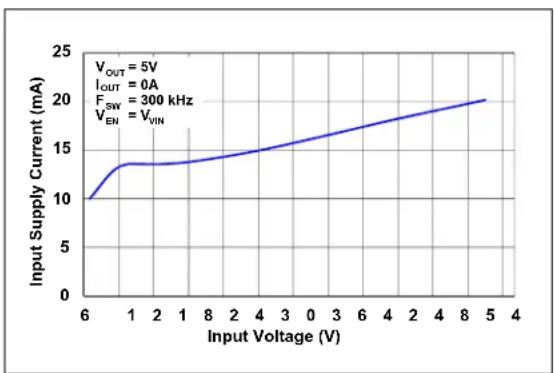
| Input Voltage (V) | Input Supply Current (mA) | | ----------------- | ------------------------- | | 6 | 10 | | 1 | 13 | | 2 | 13 | | 8 | 14 | | 4 | 15 | | 0 | 16 | | 3 | 17 | | 6 | 18 | | 2 | 19 | | 4 | 20 | | 8 | 20 | | 5 | 20 |FIGURE 2-1: Input Supply Current vs. Input Voltage.

line
| Temperature (°C) | Input Supply Current (mA) - EXTVDDD = GND | Input Supply Current (mA) - VEXTVDD = VOUT | | ---------------- | ---------------------------------------- | ------------------------------------------ | | -50 | 1.1 | 0.8 | | 0 | 1.2 | 0.9 | | 25 | 1.3 | 1.0 | | 50 | 1.4 | 1.1 | | 75 | 1.5 | 1.2 | | 100 | 1.6 | 1.3 |FIGURE 2-4: Input Supply Current vs. Temperature (HLL Mode).
line
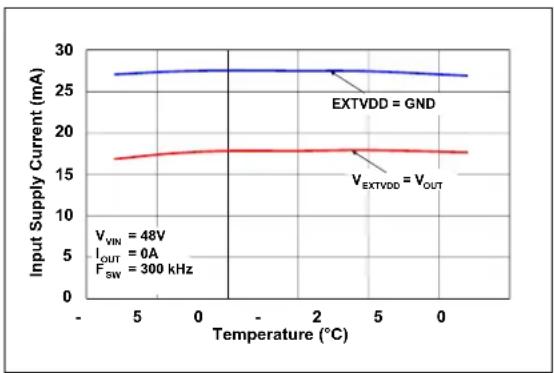
| Temperature (°C) | Input Supply Current (mA) | | ---------------- | ------------------------- | | 0 | 27.0 | | 2 | 27.0 | | 5 | 27.0 | | 0 | 27.0 |FIGURE 2-2: Input Supply Current vs. Temperature.

line
| Input Voltage (V) | Input Current (µA) | | ----------------- | ------------------ | | 6 | 50 | | 18 | 120 | | 30 | 200 | | 42 | 300 | | 54 | 400 | | 66 | 500 | | 78 | 550 |FIGURE 2-5: Input Shutdown Current vs. Input Voltage.
line
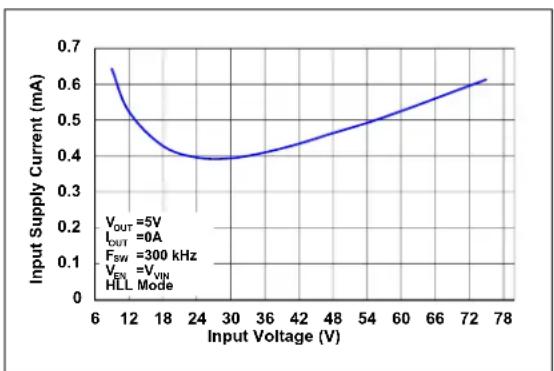
| Input Voltage (V) | Input Supply Current (mA) | | ----------------- | ------------------------- | | 6 | 0.65 | | 12 | 0.55 | | 18 | 0.45 | | 24 | 0.40 | | 30 | 0.40 | | 36 | 0.42 | | 42 | 0.45 | | 48 | 0.48 | | 54 | 0.52 | | 60 | 0.55 | | 66 | 0.58 | | 72 | 0.60 | | 78 | 0.62 |FIGURE 2-3: Input Supply Current vs. Input Voltage (HLL Mode).

line
| Temperature (C) | Input Current (µA) | | --------------- | ------------------ | | -50 | 300 | | -25 | 300 | | 0 | 305 | | 25 | 300 | | 50 | 300 | | 75 | 300 | | 100 | 300 |FIGURE 2-6: Input Shutdown Current vs. Temperature.
Note: Unless otherwise indicated, V_VIN = 12V , f_SW = 300kHzCL = 1.3k , L = 10 , VXTVDD = V_OUT , T_A = +25^ (refer to the Typical Application Circuit circuit).
line
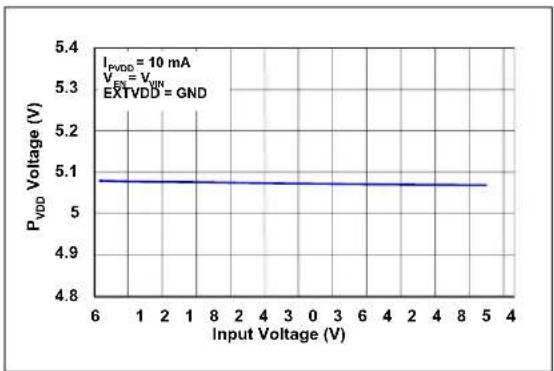
| Input Voltage (V) | P_VDD Voltage (V) | | ----------------- | ----------------- | | 6 | 5.1 | | 5 | 5.08 |FIGURE 2-7: P
V_DD Line Regulation.
line
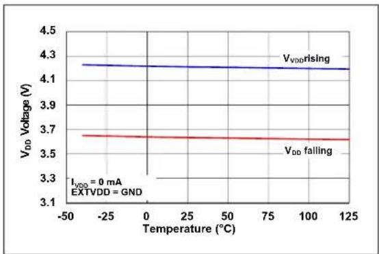
| Temperature (°C) | VDD Rising (V) | VDD Falling (V) | | ---------------- | -------------- | --------------- | | -50 | 4.2 | 3.7 | | 0 | 4.2 | 3.7 | | 25 | 4.2 | 3.7 | | 50 | 4.2 | 3.7 | | 75 | 4.2 | 3.7 | | 100 | 4.2 | 3.7 | | 125 | 4.2 | 3.7 |FIGURE 2-10: V Temperature.
_DD UVLO Threshold vs.

line
| Temperature (°C) | P_VDD Voltage (V) | | ---------------- | ----------------- | | 5 | 5.1 | | 2 | 5.05 | | 0 | 5.0 |FIGURE 2-8: P Temperature.
V_DD Voltage vs.
line
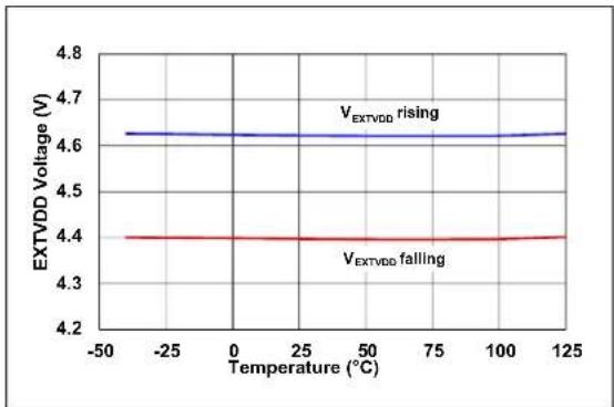
| Temperature (°C) | V_EXTVDD rising (V) | V_EXTVDD falling (V) | | ---------------- | ------------------- | -------------------- | | -50 | 4.6 | 4.4 | | 0 | 4.6 | 4.4 | | 25 | 4.6 | 4.4 | | 50 | 4.6 | 4.4 | | 75 | 4.6 | 4.4 | | 100 | 4.6 | 4.4 | | 125 | 4.6 | 4.4 |FIGURE 2-11: EXTVDD Threshold vs. Temperature.
line
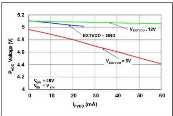
| I_PVDD (mA) | P_VDD Voltage (V) - V_EXTVDD - 12V | P_VDD Voltage (V) - V_EXTVDD = 5V | P_VDD Voltage (V) - V Vin = 48V | | ----------- | ---------------------------------- | --------------------------------- | ------------------------------- | | 0 | 5.1 | 4.9 | 4.8 | | 10 | 5.1 | 4.8 | 4.7 | | 20 | 5.1 | 4.7 | 4.6 | | 30 | 5.1 | 4.6 | 4.5 | | 40 | 5.1 | 4.5 | 4.4 | | 50 | 5.1 | 4.4 | 4.3 | | 60 | 5.1 | 4.3 | 4.2 |FIGURE 2-9: P
VDD Load Regulation.

line
| Temperature (°C) | V_EN rising | V_EN falling | | ---------------- | ----------- | ------------ | | -50 | 1.2 | 1.1 | | 0 | 1.15 | 1.05 | | 25 | 1.1 | 1.0 | | 50 | 1.05 | 0.95 | | 75 | 1.0 | 0.9 | | 100 | 0.95 | 0.85 | | 125 | 0.9 | 0.8 |FIGURE 2-12: Enable Threshold vs. Temperature.
Note: Unless otherwise indicated, V_VIN = 12V , f_SW = 300kHzCL ≈ 1.3k , L = 10 H , VXTVDD = V_OUT , T_A = +25^ C (refer to the Typical Application Circuit circuit).

line
| Temperature (°C) | EN Current (μA) | | ---------------- | --------------- | | -50 | 4.6 | | 0 | 4.6 | | 25 | 4.6 | | 50 | 4.7 | | 75 | 4.8 | | 100 | 4.9 | | 125 | 5.0 | | >125 | 5.1 | | >125 | 5.2 | | >125 | 5.3 | | >125 | 5.4 |FIGURE 2-13: Enable Bias Current vs. Temperature.
line
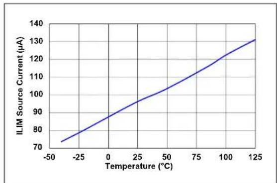
| Temperature (°C) | ILIM Source Current (µA) | | ---------------- | ------------------------ | | -50 | 70 | | -25 | 80 | | 0 | 90 | | 25 | 100 | | 50 | 105 | | 75 | 115 | | 100 | 125 | | 125 | 130 |FIGURE 2-16: I LIM Source Current vs. Temperature.
line
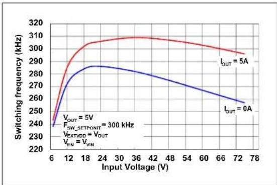
| Input Voltage (V) | Switching frequency (kHz) - IOUT = 5A | Switching frequency (kHz) - IOUT = 0A | | ----------------- | ------------------------------------ | ------------------------------------ | | 6 | 240 | 240 | | 12 | 290 | 270 | | 18 | 305 | 285 | | 24 | 310 | 285 | | 30 | 310 | 280 | | 36 | 310 | 275 | | 42 | 310 | 270 | | 48 | 305 | 265 | | 54 | 300 | 260 | | 60 | 295 | 255 | | 66 | 290 | 250 | | 72 | 285 | 245 | | 78 | 280 | 240 |FIGURE 2-14: Switching Frequency vs. Input Voltage.
line
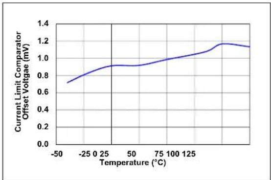
| Temperature (°C) | Current Limit Comparator Offset Volga (mV) | | ---------------- | ------------------------------------------ | | -50 | 0.7 | | 0 | 0.9 | | 25 | 0.9 | | 50 | 0.9 | | 75 | 1.0 | | 100 | 1.1 | | 125 | 1.2 | | 150 | 1.15 |FIGURE 2-17: Current Limit Comparator Offset vs Temperature.

line
| Load Current (A) | Switching Frequency (kHz) TA=85°C | Switching Frequency (kHz) TA=-40°C | Switching Frequency (kHz) TA=25°C | | ---------------- | ---------------------------------- | ---------------------------------- | ---------------------------------- | | 0 | 275 | 270 | 268 | | 1 | 285 | 280 | 278 | | 2 | 290 | 285 | 285 | | 3 | 295 | 290 | 292 | | 4 | 300 | 295 | 298 | | 5 | 305 | 300 | 302 |FIGURE 2-15: Switching Frequency vs. Load Current.

line
| Temperature (°C) | Feedback Voltage (mV) | | ---------------- | --------------------- | | -50 | 601.0 | | -25 | 600.5 | | 0 | 600.0 | | 25 | 599.5 | | 50 | 599.0 | | 75 | 598.8 | | 100 | 598.7 | | 125 | 598.6 |FIGURE 2-18: Feedback Voltage vs. Temperature.
Note: Unless otherwise indicated, V_VIN = 12V , f_SW = 300kHzCL = 1.3k , L = 10 , VXTVDD = V_OUT , T_A = +25^ (refer to the Typical Application Circuit circuit).

line
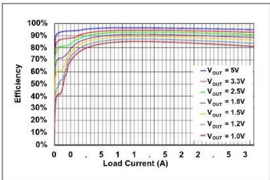
| Output Current (A) | VOUT = 1.0V | VOUT = 1.2V | VOUT = 1.5V | VOUT = 1.8V | VOUT = 2.5V | VOUT = 3.3V | VOUT = 5V | | ------------------ | ----------- | ----------- | ----------- | ----------- | ----------- | ----------- | --------- | | 0 | 0% | 0% | 0% | 0% | 0% | 0% | 0% | | 5 | ~85% | ~87% | ~88% | ~89% | ~90% | ~91% | ~92% | | 1 | ~90% | ~91% | ~92% | ~93% | ~94% | ~95% | ~96% | | 2 | ~92% | ~93% | ~94% | ~95% | ~96% | ~97% | ~98% | | 5 | ~95% | ~96% | ~97% | ~98% | ~99% | ~99.5% | ~99.8% | | 3 | ~97% | ~98% | ~99% | ~99.5% | ~99.8% | ~99.9% | ~99.95% |FIGURE 2-19: Efficiency vs. Output Current (Input Voltage = 12V, CCM Mode).

line
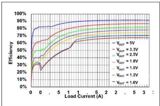
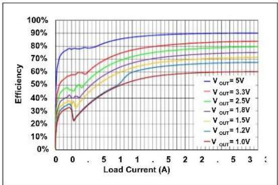
| Output Current (A) | V_OUT = 1.0V | V_OUT = 1.2V | V_OUT = 1.5V | V_OUT = 1.8V | V_OUT = 2.5V | V_OUT = 3.3V | V_OUT = 5V | | ------------------ | ------------ | ------------ | ------------ | ------------ | ------------ | ------------ | ---------- | | 0 | 0% | 0% | 0% | 0% | 0% | 0% | 0% | | 5 | ~60% | ~70% | ~75% | ~80% | ~85% | ~90% | ~95% | | 1 | ~70% | ~80% | ~85% | ~90% | ~95% | ~98% | ~99% | | 2 | ~75% | ~85% | ~90% | ~95% | ~98% | ~99% | ~99.5% | | 3 | ~80% | ~90% | ~95% | ~98% | ~99% | ~99.5% | ~99.8% |FIGURE 2-22: Efficiency vs. Output Current (Input Voltage = 48V, CCM Mode).

line
| Output Current (A) | V_OUT = 1.0V | V_OUT = 1.2V | V_OUT = 1.5V | V_OUT = 1.8V | V_OUT = 2.5V | V_OUT = 3.3V | V_OUT = 5V | | ------------------ | ------------ | ------------ | ------------ | ------------ | ------------ | ------------ | ---------- | | 0 | 0% | 0% | 0% | 0% | 0% | 0% | 0% | | 5 | ~70% | ~75% | ~80% | ~85% | ~90% | ~92% | ~95% | | 1 | ~75% | ~80% | ~85% | ~90% | ~92% | ~94% | ~96% | | 2 | ~78% | ~82% | ~87% | ~89% | ~93% | ~95% | ~97% | | 5 | ~80% | ~84% | ~88% | ~90% | ~94% | ~96% | ~97% | | 3 | ~82% | ~85% | ~89% | ~91% | ~95% | ~96% | ~97% |FIGURE 2-20: Efficiency vs. Output Current (Input Voltage = 24V, CCM Mode).

line
| Output Current (A) | VOUT = 1.0V | VOUT = 1.2V | VOUT = 1.5V | VOUT = 1.8V | VOUT = 2.5V | VOUT = 3.3V | VOUT = 5V | | ------------------ | ----------- | ----------- | ----------- | ----------- | ----------- | ----------- | --------- | | 0 | 0% | 0% | 0% | 0% | 0% | 0% | 0% | | 5 | ~40% | ~60% | ~70% | ~75% | ~80% | ~85% | ~90% | | 1 | ~50% | ~70% | ~80% | ~85% | ~90% | ~95% | ~98% | | 2 | ~55% | ~75% | ~85% | ~90% | ~95% | ~98% | ~99% | | 3 | ~60% | ~80% | ~90% | ~95% | ~98% | ~99% | ~99.5% |FIGURE 2-23: Efficiency vs. Output Current (Input Voltage = 60V, CCM Mode).

line
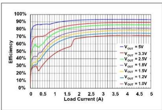
| Output Current (A) | VOUT = 1.0V | VOUT = 1.2V | VOUT = 1.5V | VOUT = 1.8V | VOUT = 2.5V | VOUT = 3.3V | VOUT = 5V | | ------------------ | ----------- | ----------- | ----------- | ----------- | ----------- | ----------- | --------- | | 0 | 0% | 0% | 0% | 0% | 0% | 0% | 0% | | 0.5 | ~10% | ~15% | ~20% | ~25% | ~30% | ~35% | ~40% | | 1 | ~30% | ~40% | ~50% | ~60% | ~70% | ~75% | ~80% | | 1.5 | ~50% | ~65% | ~75% | ~80% | ~85% | ~90% | ~92% | | 2 | ~65% | ~75% | ~85% | ~90% | ~92% | ~94% | ~95% | | 2.5 | ~70% | ~80% | ~90% | ~92% | ~94% | ~95% | ~96% | | 3 | ~72% | ~82% | ~92% | ~94% | ~95% | ~96% | ~97% | | 3.5 | ~73% | ~83% | ~93% | ~95% | ~96% | ~97% | ~98% | | 4 | ~74% | ~84% | ~94% | ~96% | ~97% | ~98% | ~98.5% | | 4.5 | ~75% | ~85% | ~95% | ~97% | ~98% | ~98.5% | ~99% | | 5 | ~76% | ~86% | ~96% | ~98% | ~98.5% | ~99% | ~99.5% |FIGURE 2-21: Efficiency vs. Output Current (Input Voltage = 36V, CCM Mode).

line
| Output Current (A) | VOUT = 1.0V | VOUT = 1.2V | VOUT = 1.5V | VOUT = 1.8V | VOUT = 2.5V | VOUT = 3.3V | VOUT = 5V | | ------------------ | ----------- | ----------- | ----------- | ----------- | ----------- | ----------- | --------- | | 0 | 0% | 0% | 0% | 0% | 0% | 0% | 0% | | 5 | ~60% | ~70% | ~65% | ~60% | ~55% | ~50% | ~45% | | 1 | ~70% | ~80% | ~75% | ~70% | ~65% | ~60% | ~55% | | 2 | ~75% | ~85% | ~80% | ~75% | ~70% | ~65% | ~60% | | 3 | ~80% | ~90% | ~85% | ~80% | ~75% | ~70% | ~65% |FIGURE 2-24: Efficiency vs. Output Current (Input Voltage = 75V, CCM Mode).
Note: Unless otherwise indicated, V_VIN = 12V , f_SW = 300 kHzCL = 1.3 kΩ, L = 10 H , VXTVDD = V_OUT , T_A = +25^ C (refer to the Typical Application Circuit circuit).
line
| Load Current (A) | VOUT = 5V | VOUT = 3.3V | VOUT = 2.5V | VOUT = 1.8V | VOUT = 1.5V | VOUT = 1.2V | VOUT = 1.0V | | ---------------- | --------- | ----------- | ----------- | ----------- | ----------- | ----------- | ----------- | | 0 | 95% | 90% | 85% | 80% | 75% | 70% | 65% | | 5 | 98% | 95% | 90% | 85% | 80% | 75% | 70% | | 1 | 99% | 97% | 93% | 88% | 83% | 78% | 73% | | 2 | 99.5% | 98% | 94% | 89% | 84% | 79% | 74% | | 5 | 99.8% | 98.5% | 95% | 90% | 85% | 80% | 75% | | 3 | 99.9% | 99% | 96% | 91% | 86% | 81% | 76% |FIGURE 2-25: Efficiency vs. Output Current (Input Voltage = 12V, HLL Mode).
line
| Load Current (A) | VOUT = 5V | VOUT = 3.3V | VOUT = 2.5V | VOUT = 1.8V | VOUT = 1.5V | VOUT = 1.2V | VOUT = 1.0V | | ---------------- | --------- | ----------- | ----------- | ----------- | ----------- | ----------- | ----------- | | 0 | 80% | 60% | 40% | 30% | 20% | 10% | 5% | | 5 | 85% | 70% | 55% | 45% | 35% | 25% | 15% | | 1 | 90% | 75% | 60% | 50% | 40% | 30% | 20% | | 2 | 90% | 75% | 60% | 50% | 40% | 30% | 20% | | 5 | 90% | 75% | 60% | 50% | 40% | 30% | 20% | | 3 | 90% | 75% | 60% | 50% | 40% | 30% | 20% |FIGURE 2-28: Efficiency vs. Output Current (Input Voltage = 48V, HLL Mode).

line
| Load Current (A) | VOUT = 5V | VOUT = 3.3V | VOUT = 2.5V | VOUT = 1.8V | VOUT = 1.5V | VOUT = 1.2V | VOUT = 1.0V | | ---------------- | --------- | ----------- | ----------- | ----------- | ----------- | ----------- | ----------- | | 0 | 90% | 70% | 60% | 50% | 40% | 30% | 20% | | 0.5 | 95% | 75% | 65% | 55% | 45% | 35% | 25% | | 1 | 98% | 80% | 70% | 60% | 50% | 40% | 30% | | 1.5 | 99% | 85% | 75% | 65% | 55% | 45% | 35% | | 2 | 99.5% | 88% | 78% | 68% | 58% | 48% | 38% | | 2.5 | 99.8% | 90% | 80% | 70% | 60% | 50% | 40% | | 3 | 99.9% | 92% | 82% | 72% | 62% | 52% | 42% | | 3.5 | 99.95% | 93% | 83% | 73% | 63% | 53% | 43% | | 4 | 99.98% | 94% | 84% | 74% | 64% | 54% | 44% | | 4.5 | 99.99% | 95% | 85% | 75% | 65% | 55% | 45% | | 5 | 100% | 96% | 86% | 76% | 66% | 56% | 46% |FIGURE 2-26: Efficiency vs. Output Current (Input Voltage = 24V, HLL Mode).
line
| Load Current (A) | V_OUT = 5V | V_OUT = 3.3V | V_OUT = 2.5V | V_OUT = 1.8V | V_OUT = 1.5V | V_OUT = 1.2V | V_OUT = 1.0V | | ---------------- | ---------- | ------------ | ------------ | ------------ | ------------ | ------------ | ------------ | | 0 | 75% | 60% | 50% | 40% | 30% | 20% | 10% | | 5 | 85% | 70% | 60% | 50% | 40% | 30% | 20% | | 1 | 90% | 75% | 65% | 55% | 45% | 35% | 25% | | 2 | 92% | 78% | 68% | 58% | 48% | 38% | 28% | | 5 | 93% | 80% | 70% | 60% | 50% | 40% | 30% | | 3 | 94% | 82% | 72% | 62% | 52% | 42% | 32% |FIGURE 2-29: Efficiency vs. Output Current (Input Voltage = 60V, HLL Mode).
line
| Load Current (A) | VOUT = 5V | VOUT = 3.3V | VOUT = 2.5V | VOUT = 1.8V | VOUT = 1.5V | VOUT = 1.2V | VOUT = 1.0V | | ---------------- | --------- | ----------- | ----------- | ----------- | ----------- | ----------- | ----------- | | 0 | 80% | 60% | 40% | 30% | 20% | 10% | 5% | | 0.5 | 85% | 70% | 55% | 45% | 35% | 25% | 15% | | 1.0 | 90% | 75% | 60% | 50% | 40% | 30% | 20% | | 1.5 | 92% | 80% | 65% | 55% | 45% | 35% | 25% | | 2.0 | 93% | 82% | 68% | 58% | 48% | 38% | 28% | | 2.5 | 94% | 85% | 70% | 60% | 50% | 40% | 30% | | 3.0 | 95% | 88% | 72% | 62% | 52% | 42% | 32% | | 3.5 | 96% | 90% | 75% | 65% | 55% | 45% | 35% | | 4.0 | 97% | 92% | 78% | 68% | 58% | 48% | 38% | | 4.5 | 98% | 93% | 80% | 70% | 60% | 50% | 40% | | 5.0 | 99% | 94% | 82% | 72% | 62% | 52% | 42% |FIGURE 2-27: Efficiency vs. Output Current (Input Voltage = 36V, HLL Mode).

line
| Load Current (A) | VOUT = 5V | VOUT = 3.3V | VOUT = 2.5V | VOUT = 1.8V | VOUT = 1.5V | VOUT = 1.2V | | ---------------- | --------- | ----------- | ----------- | ----------- | ----------- | ----------- | | 0 | 70% | 40% | 30% | 20% | 10% | 5% | | 5 | 80% | 60% | 50% | 40% | 30% | 20% | | 1 | 85% | 70% | 60% | 50% | 40% | 30% | | 2 | 90% | 75% | 65% | 55% | 45% | 35% | | 3 | 90% | 75% | 65% | 55% | 45% | 35% |FIGURE 2-30: Efficiency vs. Output Current (Input Voltage = 75V, HLL Mode).
Note: Unless otherwise indicated, V_VIN = 12V , f_SW = 300kHzCL ≈ 1.3k , L = 10 H , VXTVDD = V_OUT , T_A = +25^ C (refer to the Typical Application Circuit circuit).

line
| Signal | Value | |--------|-------| | VVIN | 0 | | VOUT | 5A | | VSW | 20V | | I_L | 5A/div |FIGURE 2-31: Power-Up.
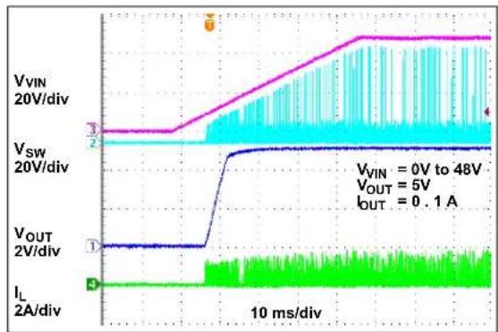
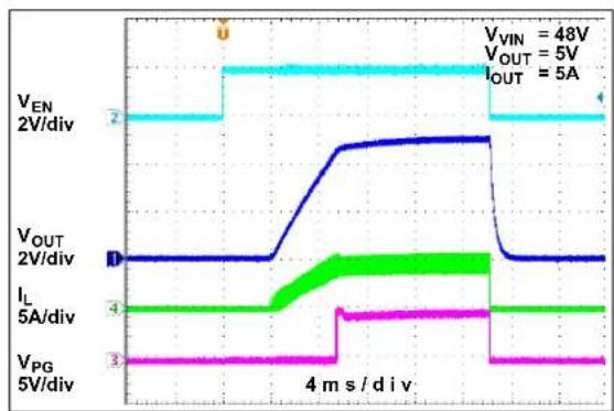
FIGURE 2-34: Power-Up at Light Load in HLL Mode ( I_OUT = 0.1 A ).
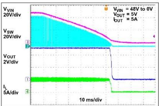
FIGURE 2-32: Power-Down.
line
| Time (ms) | VEN (V) | VOUT (V) | IL (A) | VPG (A) | |-----------|---------|----------|--------|---------| | 0 | 48 | 2 | 4 | 3 | | 1 | 48 | 2 | 4 | 3 | | 2 | 48 | 2 | 4 | 3 | | 3 | 48 | 2 | 4 | 3 | | 4 | 48 | 2 | 4 | 3 | | 5 | 48 | 2 | 4 | 3 | | 6 | 48 | 2 | 4 | 3 | | 7 | 48 | 2 | 4 | 3 | | 8 | 48 | 2 | 4 | 3 | | 9 | 48 | 2 | 4 | 3 | | 10 | 48 | 2 | 4 | 3 | | 11 | 48 | 2 | 4 | 3 | | 12 | 48 | 2 | 4 | 3 | | 13 | 48 | 2 | 4 | 3 | | 14 | 48 | 2 | 4 | 3 | | 15 | 48 | 2 | 4 | 3 | | 16 | 48 | 2 | 4 | 3 | | 17 | 48 | 2 | 4 | 3 | | 18 | 48 | 2 | 4 | 3 | | 19 | 48 | 2 | 4 | 3 | | 20 | 48 | 2 | 4 | 3 | | 21 | 48 | 2 | 4 | 3 | | 22 | 48 | 2 | 4 | 3 | | 23 | 48 | 2 | 4 | 3 | | 24 | 48 | 2 | 4 | 3 | | 25 | 48 | 2 | 4 | 3 | | 26 | 48 | 2 | 4 | 3 | | 27 | 48 | 2 | 4 | 3 | | 28 | 48 | 2 | 4 | 3 | | 29 | 48 | 2 | 4 | 3 | | 30 | 48 | 2 | 4 | 3 | | 31 | 48 | 2 | 4 | 3 | | 32 | 48 | 2 | 4 | 3 | | 33 | 48 | 2 | 4 | 3 | | 34 | 48 | 2 | 4 | 3 | | 35 | 48 | 2 | 4 | 3 | | 36 | 48 | 2 | 4 | 3 | | 37 | 48 | 2 | 4 | 3 | | 38 | 48 | 2 | 4 | 3 | | 39 | 48 | 2 | 4 | 3 | | 40 | - | - | - | - | | Peak | - | - | - | - | | Final | - | - | - | - | | Current (I_L) = -0.5A / -0.5A / -0.5A / -0.5A / -0.5A / -0.5A / -0.5A / -0.5A / -0.5A / -0.5A / -0.5A / -0.5A / -0.5A / -0.5A / -0.5A / -0.5A / -0.5A / -0.1A / -0.1A / -0.1A / -0.1A / -0.1A / -0.1A / -0.1A / -0.1A / -0.1A / -0.1A / -0.1A / -0.1A / -0.1A / -0.1A / -0.1A / -0.1A / -0.1A / -1.0A / -0.1A / -0.1A / -0.1A / -0.1A / -0.1A / -0.1A / -0.1A / -0.1A / -0.1A / -0.1A / -0.1A / -0.1A / -0.1A / -0.1A / -0.1A / -0.1A / -2.0A / -0.1A / -0.1A / -0.1A / -0.1A / -0.1A / -0.1A / -0.1A / -0.1A / -0.1A / -0.1A / -0.1A / -0.1A / -0.1A / -0.1A / -0.1A / -0.1A/ -0.1A/ -0.1A/ -0.1A/ -0.1A/ -0.1A/ -0.1A/ -0.1A/ -0.1A/ -0.1A/ -0.1A/ -0.1A/ -0.1A/ -0.1A/ -0.1A/ -0.1A/ -0.1A/ -0.75A/ -0.75A/ -0.75A/ -0.75A/ -0.75A/ -0.75A/ -0.75A/ -0.75A/ -0.75A/ -0.75A/ -0.75A/ -0.75A/ -0.75A/ -0.75A/ -0.75A(+) | | Current (I_L) = -0.5A / -0.5A / -0.5A / -0.5A / -0.5A / -0.5A / -0.5A / -0.5A / -0.5A / -0.5A / -0.5A / -0.5A / -0.5A / -0.5A / -0.5A / --) | | Current (I_L) = -0.5A / --(-) * (I_PG) = (-) * (V_PG) = (-) * (V_OUT) = (-) * (V_VIN) = (-) * (V_OUT) = (-) * (V_OUT) = (-) * (V_OUT) = (-) * (V_OUT) = (-) * (V_OUT) = (-) * (V_OUT) = (-) * (V_OUT) = (-) * (V_OUT) = (-) * (V_OUT) = (-) * (V_OUT) = (-) * (V_OUT) = (-) * (V_OUT) = (-) * (V_OUT) = (-)FIGURE 2-35: Enable Turn-On/Turn-Off.
line
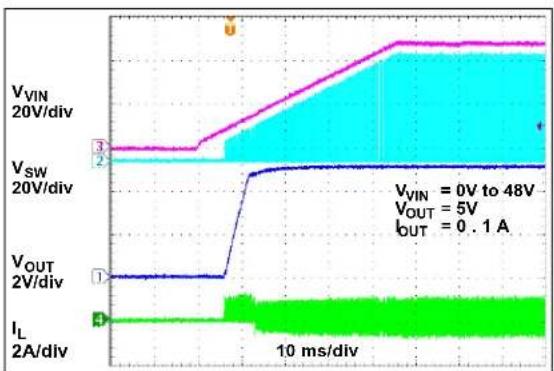
| Parameter | Value | | --------- | --------- | | VVIN | 0V | | VOUT | 5V | | IOUT | 0.1A | | VSW | 20V/div | | IL | 2A/div |FIGURE 2-33: Power-Up at Light Load in CCM Mode ( I_OUT = 0.1 A ).
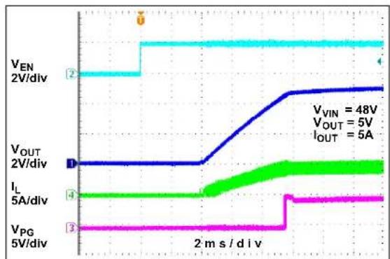
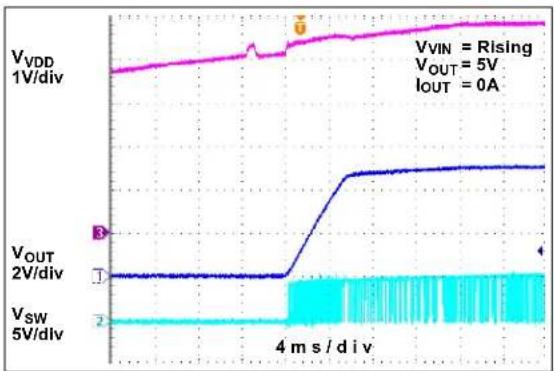
FIGURE 2-36: Enable Turn-On Delay.
Note: Unless otherwise indicated, V_VIN = 12V , f_SW = 300kHzCL ≈ 1.3k , L = 10 H , VXTVDD = V_OUT , T_A = +25^ C (refer to the Typical Application Circuit circuit).
line
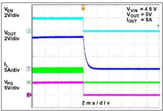
| Signal | Value | |--------|-----------| | VEN | 48 V | | VOUT | 5 V | | IOUT | 5 A | | IL | 5 A/div | | VPG | 5 V/div |FIGURE 2-37: Enable Turn-Off Delay.

line
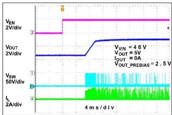
| Parameter | Value | | ----------------- | --------- | | VEN / 2V/div | 3 | | VOUT / 2V/div | 3 | | VOUT_PREBIAS | 3 | | VWIN / 5V | 48 | | IOUT / 0A | 0 | | VSW / 50V | P | | IL / 2A/div | 4 |FIGURE 2-40: Enable Turn-On with Prebiased Output (CCM Mode).

line
| Signal | Value | |--------|-------| | VVIN | 4.8 V | | VOUT | 5 V | | IOUT | 0.2 A | | I_L | 4 A | | VPG | 0.2 A | | 10 ms/div | 0.2 A |FIGURE 2-38: Enable Turn-On/Turn-Off at Light Load in CCM Mode.
line
| Signal | Value | |-----------------|-----------| | VEN | 4.8 V | | VOUT | 5 V | | VOUT_PREBIAS | 2.5 V | | VSW | P | | IL | 3 A |FIGURE 2-41: Enable Turn-On with Prebiased Output (HLL Mode).

line
| Signal | Value | |--------|-----------| | VEN | 48V | | VOUT | 5V | | IOUT | 0.2 A | | IL | 4A/Div | | VPG | 5V/Div |FIGURE 2-39: Enable Turn-On/Turn-Off at Light Load in HLL Mode.
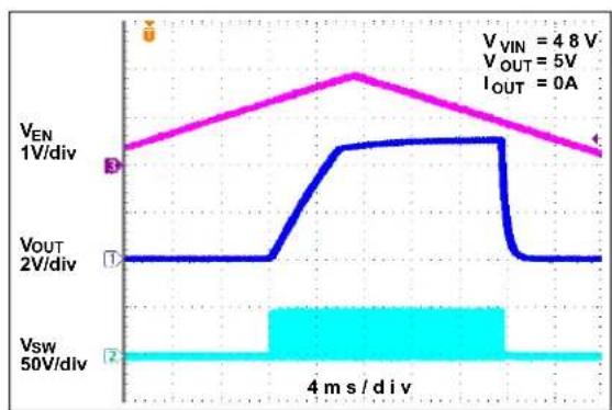
FIGURE 2-42: Enable Thresholds.
Note: Unless otherwise indicated, V_VIN = 12V , f_SW = 300kHzCL ≈ 1.3k , L = 10 H , VXTVDD = V_OUT , T_A = +25^ C (refer to the Typical Application Circuit circuit).
line
| Time (ms) | VVDD (1V/div) | VOUT (2V/div) | VSW (5V/div) | |-----------|---------------|---------------|--------------| | 0 | ~0.8 | 0 | 0 | | 1 | ~0.9 | 0 | 0 | | 2 | ~0.95 | 0 | 0 | | 3 | ~0.98 | 0 | 0 | | 4 | ~1.0 | 0 | 0 | | 5 | ~1.0 | 0 | 0 | | 6 | ~1.0 | 0 | 0 | | 7 | ~1.0 | 0 | 0 | | 8 | ~1.0 | 0 | 0 | | 9 | ~1.0 | 0 | 0 | | 10 | ~1.0 | 0 | 0 | | 11 | ~1.0 | 0 | 0 | | 12 | ~1.0 | 0 | 0 | | 13 | ~1.0 | 0 | 0 | | 14 | ~1.0 | 0 | 0 | | 15 | ~1.0 | 0 | 0 | | 16 | ~1.0 | 0 | 0 | | 17 | ~1.0 | 0 | 0 | | 18 | ~1.0 | 0 | 0 | | 19 | ~1.0 | 0 | 0 | | 20 | ~1.0 | 0 | 0 | | 21 | ~1.0 | 0 | 0 | | 22 | ~1.0 | 0 | 0 | | 23 | ~1.0 | 0 | 0 | | 24 | ~1.0 | 0 | 0 | | 25 | ~1.0 | 0 | 0 | | 26 | ~1.0 | 0 | 0 | | 27 | ~1.0 | 0 | 0 | | 28 | ~1.0 | 0 | 0 | | 29 | ~1.0 | 0 | 0 | | 30 | ~1.0 | 0 | 0 | | 31 | ~1.0 | 0 | 0 | | 32 | ~1.0 | 0 | 0 | | 33 | ~1.0 | 0 | 0 | | 34 | ~1.0 | 0 | 0 | | 35 | ~1.0 | 0 | 0 | | 36 | ~1.0 | 0 | 0 | | 37 | ~1.0 | 0 | 0 | | 38 | ~1.0 | 0 | 0 | | 39 | ~1.0 | 0 | 0 | | 40 | ~1.0 | 0 | 0 | | 41 | ~1.0 | 0 | 0 | | 42 | ~1.0 | 0 | 0 | | 43 | ~1.0 | 0 | 0 | | 44 | ~1.0 | 0 | 0 | | 45 | ~1.0 | 0 | 0 | | 46 | ~1.0 | 0 | 0 | | 47 | ~1.0 | 0 | 0 | | 48 | ~1.0 | 0 | 0 | | 49 | ~1.0 | 0 | 0 | | 50 | ~1.0 | 0 | 0 | | 51 | ~1.0 | 0 | 0 | | 52 | ~1.0 | 0 | 0 | | 53 | ~1.0 | 0 | 0 | | 54 | ~1.0 | 0 | 0 | | 55 | ~1.0 | 0 | 0 | | 56 | ~1.0 | 0 | 0 | | 57 | ~1.0 | 0 | 0 | | 58 | ~1.0 | 0 | 0 | | 59 | ~1.0 | 0 | 0 | | 60 | ~1.0 | 0 | 0 | | 61 | ~1.0 | 0 | 0 | | 62 | ~1.0 | 0 | 0 | | 63 | ~1.0 | 0 | 0 | | 64 | ~1.0 | 0 | 0 | | 65 | ~1.0 | 0 | 0 | | 66 | ~1.0 | 0 | 0 | | 67 | ~1.0 | 0 | 0 | | 68 | ~1.0 | 0 | 0 | | 69 | ~1.0 | 0 | 0 | | 70 | ~1.0 | 0 | 0 | | 71 | ~1.0 | 0 | - | | 72 | ~1.0 | - | - | | 73 | ~1.0 | - | - | | 74 | ~1.0 | - | - | | 75 | ~1.0 | - | - | | 76 | ~1.0 | - | - | | 77 | ~1.0 | - | - | | 78 | ~1.0 | - | - | | 79 | ~1.0 | - | - | | 80 | ~1.0 | - | - | | Note: The data is extracted from the code and displayed on the screen above as it is not available for this image in the provided code format.FIGURE 2-43: V _DD UVLO Threshold-Rising.
line
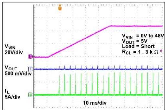
| Time (ms) | V Vin (20V/div) | VOUT (500 mV/div) | I_L (5A/div) | |-----------|-----------------|-------------------|--------------| | 0 | 0 | 5 | 0 | | 10 | ~0.5 | ~0.5 | ~0 | | 20 | ~1.0 | ~0.5 | ~0 | | 30 | ~1.5 | ~0.5 | ~0 | | 40 | ~2.0 | ~0.5 | ~0 | | 50 | ~2.5 | ~0.5 | ~0 | | 60 | ~3.0 | ~0.5 | ~0 | | 70 | ~3.5 | ~0.5 | ~0 | | 80 | ~4.0 | ~0.5 | ~0 | | 90 | ~4.5 | ~0.5 | ~0 | | 100 | ~5.0 | ~0.5 | ~0 | | 110 | ~5.5 | ~0.5 | ~0 | | 120 | ~6.0 | ~0.5 | ~0 | | 130 | ~6.5 | ~0.5 | ~0 | | 140 | ~7.0 | ~0.5 | ~0 | | 150 | ~7.5 | ~0.5 | ~0 | | 160 | ~8.0 | ~0.5 | ~0 | | 170 | ~8.5 | ~0.5 | ~0 | | 180 | ~9.0 | ~0.5 | ~0 | | 190 | ~9.5 | ~0.5 | ~0 | | 200 | 10.0 | 1 | 0 | | 210 | 10.5 | 1 | 0 | | 220 | 11.0 | 1 | 0 | | 230 | 11.5 | 1 | 0 | | 240 | 12.0 | 1 | 0 | | 250 | 12.5 | 1 | 0 | | 260 | 13.0 | 1 | 0 | | 270 | 13.5 | 1 | 0 | | 280 | 14.0 | 1 | 0 | | 290 | 14.5 | 1 | 0 | | 300 | 15.0 | 1 | 0 | | 310 | 15.5 | 1 | 0 | | 320 | 16.0 | 1 | 0 | | 330 | 16.5 | 1 | 0 | | 340 | 17.0 | 1 | 0 | | 350 | 17.5 | 1 | 0 | | 360 | 18.0 | 1 | 0 | | 370 | 18.5 | 1 | 0 | | 380 | 19.0 | 1 | 0 | | 390 | 19.5 | 1 | 0 | | 400 | 20.0 | 1 | 0 | | 410 | 20.5 | 1 | 0 | | 420 | 21.0 | 1 | 0 | | 430 | 21.5 | 1 | 0 | | 440 | 22.0 | 1 | 0 | | 450 | 22.5 | 1 | 0 | | 460 | 23.0 | 1 | 0 | | 470 | 23.5 | 1 | 0 | | 480 | 24.0 | 1 | 0 | | 490 | 24.5 | 1 | 0 | | 500 | 25.0 | 1 | 0 | | ... | ... | ... | ... | | ... | ... | ... | ... | | ... | ... | ... | ... | | ... | ... | ... | ... | | ... | ... | ... | ... | | ... | ... | ... | ... | | ... | ... | ... | ... | | ... | ... | ... | ... | | ... | ... |... | ... | | ... | ... | ... | ... | | ... | ... | ... | ... | | ... | ... | ... | ... | | ... | ... | ... | ... | | ... | ... | ... | ... | | ... | ... | ... | ... | | ... | ... | ... | ... | | ... [Note] VVIN = 2V to VOUT = VOUT = Short, Load = Short, RCL = -1.3 kΩ]FIGURE 2-46: Power-Up into Output Short.
line
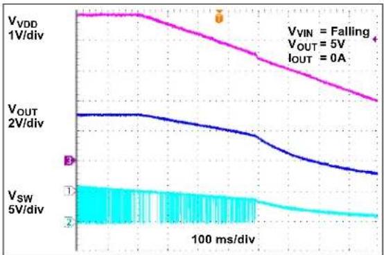
| Time (ms) | VDD (1V/div) | VOUT (2V/div) | VSW (5V/div) | |-----------|--------------|---------------|--------------| | 0 | High | Low | Low | | 100 | Decreasing | Decreasing | Decreasing |FIGURE 2-44: V _DD UVLO Threshold-Falling.

line
| Time (ms) | VOUT (2V/div) | IOUT (5A/div) | |-----------|---------------|---------------| | 0 | 48 | 5 | | 2 | 48 | 5 | | 4 | 48 | 5 | | 6 | 48 | 5 | | 8 | 48 | 5 | | 10 | 48 | 5 | | 12 | 48 | 5 | | 14 | 48 | 5 | | 16 | 48 | 5 | | 18 | 48 | 5 | | 20 | 48 | 5 | | 22 | 48 | 5 | | 24 | 48 | 5 | | 26 | 48 | 5 | | 28 | 48 | 5 | | 30 | 48 | 5 | | 32 | 48 | 5 | | 34 | 48 | 5 | | 36 | 48 | 5 | | 38 | 48 | 5 | | 40 | 48 | 5 | | 42 | 48 | 5 | | 44 | 48 | 5 | | 46 | 48 | 5 | | 48 | 48 | 5 | | 50 | 48 | 5 | | 52 | 48 | 5 | | 54 | 48 | 5 | | 56 | 48 | 5 | | 58 | 48 | 5 | | 60 | 48 | 5 | | 62 | 48 | 5 | | 64 | 48 | 5 | | 66 | 48 | 5 | | 68 | 48 | 5 | | 70 | 48 | 5 | | 72 | 48 | 5 | | 74 | 48 | 5 | | 76 | 48 | 5 | | 78 | 48 | 5 | | 80 | 48 | 5 | | 82 | 48 | 5 | | 84 | 48 | 5 | | 86 | 48 | 5 | | 88 | 48 | 5 | | 90 | 48 | 5 | | 92 | 48 | 5 | | 94 | 48 | 5 | | 96 | 48 | 5 | | 98 | 48 | 5 | | 100 | 48 | 5 | | | | | | | | | | | | | | | | | | | | | | | | | | | | | | | | | | | | | | | | | | | | | | | | | | | | | | | | | | | | | | | | | | | | | | | | | | | | | | | | | | | | | | | | | | | | | | | | | | | | | | | | | | | | | | | | | | | | | | | | | | | | | | | | | | | | | | | | | | | | | | | | | | | | | | | | | | | | | | | | | | | | | | | | | | | | | | | | | | | | | | | | | | | | | | | | | | | | | | | | | | | | | | | | | | | | | | | | | | | | | | | | | | | | | | | | | | | | | | | | | | | | | | | | | | | | | | | | | | | | | | | | | | | | | | | | | | | | | | | | | | | | | | | | | | | | | | | | | | | | | | | | | | | | | | | | | | | | | | | | | | | | | | | | | | | | | | | | | | | | | | | | | | | | | | | | | \ | The values for the VOUT and IOUT are plotted on the graph. The VOUT and IOUT values are calculated based on the formula of the voltage output. The data is presented in a table format as shown above and below the chart. The values for the VOUT and IOUT columns are labeled as 'VOUT' and 'IOUT' respectively. The values for the IOUT column are labeled as '1.3 kΩ'.FIGURE 2-47: Output Current Limit Threshold.
line
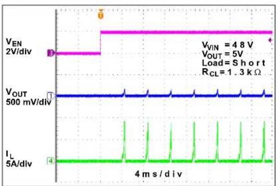
| Signal | Value | |--------|-----------| | VEN | 4.8 V | | VOUT | 5 V | | I_L | 5 A/div |FIGURE 2-45: Enable into Output Short.
line
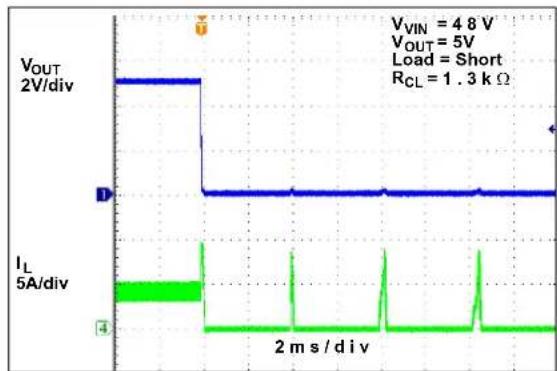
| Parameter | Value | | --------- | --------- | | V Vin | 4.8 V | | V OUT | 5 V | | Load | Short | | RCL | 1.3 kΩ | | 2 m s / div | Current | | IL | 5 A/div |FIGURE 2-48: Output Short Circuit.
Note: Unless otherwise indicated, V_VIN = 12V , f_SW = 300kHzCL ≈ 1.3k , L = 10 H , VXTVDD = V_OUT , T_A = +25^ C (refer to the Typical Application Circuit circuit).
line
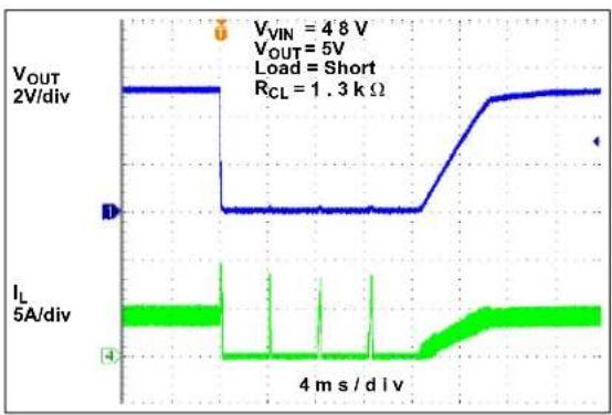
| Parameter | Value | | --------- | --------- | | V Vin | 4.8 V | | VOUT | 5 V | | Load | Short | | RCL | 1.3 kΩ | | I_L | 5 A/div |FIGURE 2-49: Recovery from Output Short Circuit.

FIGURE 2-52: Load Transient Response (CCM Mode).

line
| Time (μs) | VOUT (mV) | IOUT (A) | |-----------|-----------|----------| | 0 | 4.8 | 2 | | 100 | 4.8 | 2 | | 200 | 4.8 | 2 |FIGURE 2-50: Load Transient Response (CCM Mode).
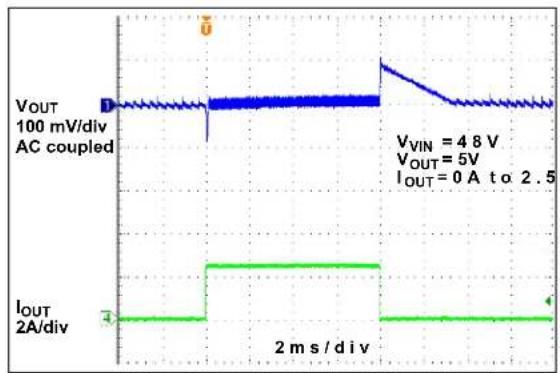
FIGURE 2-53: Load Transient Response (HLL Mode).
line
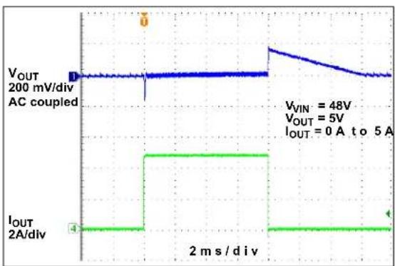
| Time (ms) | VOUT (mV) | IOUT (A) | |-----------|-----------|----------| | 0 | 200 | 2A/div | | 1 | 200 | 2A/div | | 2 | 200 | 2A/div | | 3 | 200 | 2A/div | | 4 | 200 | 2A/div | | 5 | 200 | 2A/div | | 6 | 200 | 2A/div | | 7 | 200 | 2A/div | | 8 | 200 | 2A/div | | 9 | 200 | 2A/div | | 10 | 200 | 2A/div | | 11 | 200 | 2A/div | | 12 | 200 | 2A/div | | 13 | 200 | 2A/div | | 14 | 200 | 2A/div | | 15 | 200 | 2A/div | | 16 | 200 | 2A/div | | 17 | 200 | 2A/div | | 18 | 200 | 2A/div | | 19 | 200 | 2A/div | | 20 | 200 | 2A/div | | 21 | 200 | 2A/div | | 22 | 200 | 2A/div | | 23 | 200 | 2A/div | | 24 | 200 | 2A/div | | 25 | 200 | 2A/div | | 26 | 200 | 2A/div | | 27 | 200 | 2A/div | | 28 | 200 | 2A/div | | 29 | 200 | 2A/div | | 30 | 200 | 2A/div | | 31 | 200 | 2A/div | | 32 | 200 | 2A/div | | 33 | 200 | 2A/div | | 34 | 200 | 2A/div | | 35 | 200 | 2A/div | | 36 | 200 | 2A/div | | 37 | 200 | 2A/div | | 38 | 200 | 2A/div | | 39 | 200 | 2A/div | | 40 | 200 | 2A/div | | 41 | 200 | 2A/div | | 42 | 200 | 2A/div | | 43 | 200 | 2A/div | | 44 | 200 | 2A/div | | 45 | 200 | 2A/div | | 46 | 200 | 2A/div | | 47 | 200 | 2A/div | | 48 | 200 | 2A/div | | 49 | 200 | 2A/div | | 50 | 200 | 2A/div | | Note: The VOUT values are calculated based on the AC coupled voltage and current values. The IOUT values are calculated as the sum of the two input voltages. There is no label for the output voltage values. The IOUT values are calculated as the sum of the two input voltages. There is no label for the output voltage values. The IOUT values are calculated as the sum of the two input voltages. There is no label for the output voltage values. The IOUT values are calculated as the sum of the two input voltages. There is no label for the output voltage values. The IOUT values are calculated as the sum of the two input voltages. There is no labels for the output voltage values. The IOUT values are calculated as the sum of the two input voltages. There is no labels for the output voltage values. The IOUT values are calculated as the sum of the two input voltages. There is no labels for the output voltage values. The IOUT values are calculated as the sum of the two input voltages. There is no labels for the output voltage values. The IOUT values are calculated as the sum of the two input voltages.FIGURE 2-51: Load Transient Response (HLL Mode).
line
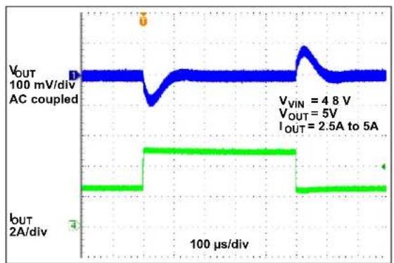
| Parameter | Value | | --------------- | --------- | | V Vin | 4.8 V | | V OUT | 5 V | | I OUT | 2.5A to 5A |FIGURE 2-54: Load Transient Response (HLL Mode).
Note: Unless otherwise indicated, V_VIN = 12V , f_SW = 300kHzCL ≈ 1.3k , L = 10 H , VXTVDD = V_OUT , T_A = +25^ C (refer to the Typical Application Circuit circuit).

line
| Time (μs) | VOUT (mV) | IL (A) | VSW (V) | |-----------|-----------|--------|---------| | 0 | 48 | 2 | 0 | | 2 | 48 | 2 | 0 | | 4 | 48 | 2 | 0 | | 6 | 48 | 2 | 0 | | 8 | 48 | 2 | 0 | | 10 | 48 | 2 | 0 | | 12 | 48 | 2 | 0 | | 14 | 48 | 2 | 0 | | 16 | 48 | 2 | 0 | | 18 | 48 | 2 | 0 | | 20 | 48 | 2 | 0 | | 22 | 48 | 2 | 0 | | 24 | 48 | 2 | 0 | | 26 | 48 | 2 | 0 | | 28 | 48 | 2 | 0 | | 30 | 48 | 2 | 0 | | 32 | 48 | 2 | 0 | | 34 | 48 | 2 | 0 | | 36 | 48 | 2 | 0 | | 38 | 48 | 2 | 0 | | 40 | 48 | 2 | 0 | | 42 | 48 | 2 | 0 | | 44 | 48 | 2 | 0 | | 46 | 48 | 2 | 0 | | 48 | 48 | 2 | 0 | | 50 | 48 | 2 | 0 | | 52 | 48 | 2 | 0 | | 54 | 48 | 2 | 0 | | 56 | 48 | 2 | 0 | | 58 | 48 | 2 | 0 | | 60 | 48 | 2 | 0 | | 62 | 48 | 2 | 0 | | 64 | 48 | 2 | 0 | | 66 | 48 | 2 | 0 | | 68 | 48 | 2 | 0 | | 70 | 48 | 2 | 0 | | 72 | 48 | 2 | 0 | | 74 | 48 | 2 | 0 | | 76 | 48 | 2 | 0 | | 78 | 48 | 2 | 0 | | 80 | 48 | 2 | 0 | | 82 | 48 | 2 | 0 | | 84 | 48 | 2 | 0 | | 86 | 48 | 2 | 0 | | 88 | 48 | 2 | 0 | | 90 | 48 | 2 | 0 | | 92 | 48 | 2 | 0 | | 94 | 48 | 2 | 0 | | 96 | 48 | 2 | 0 | | 98 | 48 | 2 | 0 | | 100 | 48 | 2 | 0 | | | | | | | | | | | | | | | | | | | | | | | | | | | | | | | | | | | | | | | | | | | | | | | | | | | | | | | | | | | | | | | | | | | | | | | | | | | | | | | | | | | | | | | | | | | | | | | | | | | | | | | | | | | | | | | | | | | | | | | | | | | | | | | | | | | | | | | | | | | | | | | | | | | | | | | | | | | | | | | | | | | | | | | | | | | | | | | | | | | | | | | | | | | | | | | | | | | | | | | | | | | | | | | | | | | | | | | | | | | | | | | | | | | | | (with label 'AC coupled') - AC coupled - IL (with label 'IL') - VSW (with label 'VSW') - Output (with label 'IOUT') - Output (with label 'IOUT') - Output (with label 'VIN') - Output (with label 'VIN') - Output (with label 'VOUT') - Output (with label 'VOUT') - Output (with label 'IOUT') - Output (with label 'IOUT') - Output (with label 'IOUT') - Output (with label 'VIN') - Output (with label 'VIN') - Output (with label 'VIN') - Output (with label 'VIN') - Output (with label 'VIN') - Output (with label 'VIN') - Output (with label 'VIN') - Output (with label 'VIN') - Output (with label 'VIN') - Output (with label 'VIN') - Output (with label 'VIN') - Output (with label 'VIN'). End: The values for AC coupled AC, IL, and VSW are calculated based on the given values of the input voltage and output voltage. The values for AC coupled AC and IL are calculated as a function of the input voltage and output voltage. The values for VSW are calculated as a function of the input voltage and output voltage. The values for Output voltage and Output current are calculated as a function of the input voltage and output current. The values for Output current and Output voltage are calculated as a function of the input voltage and output voltage. The values for Output current and Output voltage are calculated as a function of the input voltage and output voltage. The values for Output current and Output voltage are calculated as a function of the input voltage and output voltage. The values for Output current and Output voltage are calculated as a function of the input voltage and output voltage. The values for Output current and Output voltage are calculated as a function of the input voltage and output voltage. The values for Output current and Output voltage are calculated as a function of their respective values. The values for Output current and Output voltage are calculated as a function of their respective values. The values for Output current and Output voltage are calculated as a function of their respective values. The values for Output current and Output voltage are calculated as a function of their respective values. The values for Output current and Output voltage are calculated as a function of their respective values. The values for Output current and Output voltage are calculated as a function of their respective values. The values for Output current and Output voltage (in volts) are calculated as a function of its corresponding value. The values for Output current and Output voltage are calculated as a function of its corresponding value. The values for Output current and Output voltage are calculated as a function of its corresponding value. The values for Output current and Output voltage are calculated as a function of its corresponding value. The values for Output current and Output voltage are calculated as a function of its corresponding value. The values for Output current and Output voltage are calculated as a function of its corresponding value. The values for Output current and Output voltage are calculated as a function of its corresponding value.FIGURE 2-55: Switching Waveform at No Load (CCM Mode).
line
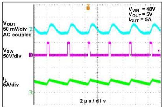
| Parameter | Value | | --------------- | --------- | | VOUT | 50 mV/div | | VSW | 50V/div | | IL | 5A/div |FIGURE 2-57: Switching Waveform at Full Load.
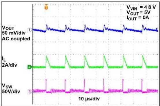
FIGURE 2-56: Switching Waveform at No Load (HLL Mode).
3.0 PIN DESCRIPTION
The descriptions of the pins are listed in Table3-1.
TABLE 3-1: PIN FUNCTION TABLE
| Pin Number Pin | Name Pin Function | |
| 1 PG Open | drain Power Good Output Pin | |
| 2 | I_LIM | Current Limit Setting Resistor Connection Pin |
| 3 | SW | Switch Pin and Current Sense Input for negative current limit |
| 4 | BST | Bootstrap Capacitor Connection Pin |
| 5 DH High-side N-MOSFET Gate | Driver Output | |
| 6 | P_GND | Power Ground |
| 7 | DL | Low-side N-MOSFET Gate Driver Output |
| 8 | P_VDD | Internal Low Dropout Regulators Output of the MIC2127A |
| 9 | EXTVDD | Supply Input for the internal low voltage LDO |
| 10 | EN | Enable Input |
| 11 | FREQ | Switching Frequency Programming Input |
| 12 | MODE | Light Load Mode Selection Input |
| 13 | FB | Feedback Input |
| 14 | A_GND | Analog Ground |
| 15 | V_DD | Supply Input for the MIC2127A internal analog circuits |
| 16 | V_IN | Supply Input for the internal high-voltage LDO |
| 17 | EP | Exposed Pad |
3.1 Power Good Output Pin (PG)
Connect PG to V_DD through a pull-up resistor. PG is low when the FB voltage is 10% below the 0.6V reference voltage.
3.2 Current Limit Pin (I LIM)
Connect a resistor from I_LIM to SW to set the current limit. Refer to Section 4.3 “Current Limit (ILIM)” for more details.
3.3 Switch Pin (SW)
The SW pin provides the return path for the high-side N-MOSFET gate driver when High-Side MOSFET Gate Drive (DH) is low and is also used to sense low-side MOSFET current by monitoring the SW node voltage for negative current limit function.
Connect SW to the pin where the high-side MOSFET source and the low-side MOSFET drain terminal are connected together.
3.4 Bootstrap Capacitor Pin (BST)
BST capacitor acts as supply for the high-side N-MOSFET driver. Connect a minimum of 0.1 F low ESR ceramic capacitor between BST and SW. Refer to Section 4.5 “High-Side MOSFET Gate Drive (DH)” for more details.
3.5 High-Side N-MOSFET Gate Driver Output Pin (DH)
High-side N-MOSFET gate driver Output. Connect DH to the gate of external high-side N-MOSFET.
3.6 Power Ground Pin (P GND)
P_GND provides the return path for the internal low-side N-MOSFET gate driver output and also acts as reference for the current limit comparator. Connect P_GND to the external low-side N-MOSFET source terminal and to the return terminal of P_VDD bypass capacitor.
3.7 Low-Side N-MOSFET Gate Driver Output Pin (DL)
Low-side N-MOSFET gate driver output. Connect to the gate terminal of the external low-side N-MOSFET.
3.8 Internal Low Dropout Regulators Output Pin ( P_VDD )
Combined output of the two internal LDOs (one LDO powered by V_IN and the other LDO powered by EXTVDD). P_VDD is the supply for the low-side MOSFET driver and for the floating high-side MOSFET driver. Connect a minimum of 4.7 F low ESR ceramic capacitor from P_VDD to P_GND .
3.9 EXTVDD
Supply to the internal low voltage LDO. Connect EXTVDD to the output of the buck converter if it is between 4.7V to 14V to improve system efficiency. Bypass EXTVDD with a minimum of 1 F low ESR ceramic capacitor. Refer to Section 4.7 “Auxiliary Bootstrap LDO (EXTVDD)” for more details.
3.10 Enable Input Pin (EN)
EN is a logic input. Connect to logic high to enable the converter, and connect to logic low to disable the converter.
3.11 Switching Frequency Programming Input Pin (FREQ)
Switching Frequency Programming Input. Connect to mid-point of the resistor divider formed between V_IN and A_GND to set the switching frequency of the converter. Tie FREQ to V_IN to set the switching frequency to 800 kHz. Refer to Section 5.1 “Setting the Switching Frequency” for more details.
3.12 Light Load Mode Selection Input Pin (MODE)
Light Load Mode Selection Input. Connect MODE pin to V_DD to select Continuous Conduction mode under light loads, or connect to A_GND to select HyperLight Load (HLL) mode of operation under light loads. Refer to Section 4.2 “Light Load Operating Mode (MODE)” for further details.
3.13 Feedback Input Pin (FB)
FB is input to the transconductance amplifier of the control loop. The control loop regulates the FB voltage to 0.6V. Connect the FB node to the mid-point of the resistor divider between output and A_GND .
3.14 Analog Ground Pin (A GND)
A_GND is the reference to the analog control circuits inside the MIC2127A. Connect A_GND to P_GND at one point on the PCB.
3.15 Bias Voltage Pin (V DD)
Supply for the MIC2127A internal analog circuits. Connect V_DD to P_VDD of the MIC2127A through a low-pass filter. Connect a minimum of 4.7 F low ESR ceramic capacitor from V_DD to A_GND for decoupling.
3.16 Input Voltage Pin (V IN)
Supply Input to the internal high-voltage LDO. Connect to the main power source and bypass to P_GND with a minimum of 0.1 F low ESR ceramic capacitor.
3.17 Exposed Pad (EP)
Connect to the A_GND copper plane to improve thermal performance of the MIC2127A device.
4.0 FUNCTIONAL DESCRIPTION
The MIC2127A device is an adaptive on-time synchronous buck controller, designed to cover a wide range of input voltage applications ranging from 4.5V-5V. An adaptive on-time control scheme is employed to get a fast transient response and to obtain high-voltage conversion ratios at constant switching frequency. Overcurrent protection is implemented by sensing low-side MOSFET's R_DS(ON) , which eliminates lossy current sense resistor. The device features internal soft-start, enable input, UVLO, power good output (PG), secondary bootstrap LDO and thermal shutdown.
4.1 Theory of Operation
The MIC2127A is an adaptive on-time synchronous buck controller that operates based on ripple at the feedback node. The output voltage is sensed by the MIC2127A feedback pin (FB) and is compared to a 0.6V reference voltage ( V_REF ) at the low-gain transconductance error amplifier ( g_M ), as shown in the Functional Block Diagram. Figure 4-1 shows the MIC2127A control loop timing during steady-state operation.
The error amplifier behaves as the short circuit for the ripple voltage frequency on the FB pin, which causes the error amplifier output voltage ripple to follow the feedback voltage ripple. When the transconductance error amplifier output ( V_gM ) is below the reference voltage of the comparator, which is same as the error amplifier reference ( V_REF ), the comparator triggers and generates an on-time event. The on-time period is predetermined by the fixed t_ON estimator circuitry, which is given by Equation 4-1:
EQUATION 4-1:
$$ \begin{array}{l l} & t _ {O N E S T I M A T E D (} \quad \frac {V _ {O U T}}{V _ {V I N} \times f _ {S W}} = \ \text {Where:} \ V _ {O U T} & = \text {Output voltage} \ V _ {V I N} & = \text {Power stage input voltage} \ f _ {S W} & = \text {Switching frequency} \end{array} $$
At the end of the ON time, the internal high-side driver turns off the high-side MOSFET and the low-side driver turns on the low-side MOSFET. The OFF time of the high-side MOSFET depends on the feedback voltage. When the feedback voltage decreases, the output of the g_M amplifier ( V_gM ) also decreases. When the output of the g_M amplifier ( V_gM ) is below the reference voltage of the comparator (which is same as the error amplifier reference ( V_REF )), the OFF time ends and ON time is triggered. If the OFF time determined by the feedback voltage is less than the minimum OFF time ( t_OFF(MIN) ) of the MIC2127A, which is about 230 ns (typical), the MIC2127A control logic applies the t_OFF(MIN) , instead.
The maximum duty cycle can be calculated using Equation 4-2:
EQUATION 4-2:
$$ D _ {M A X} = \frac {t _ {S W} - t _ {O F F M I N (}}{t _ {S W}} J =) - \frac {2 3 0 n s}{t _ {S W}} $$
Where:
$$ t _ {S W} = \text { Switching period, equal to } 1 / f _ {S W} $$
It is not recommended to use the MIC2127A device with an OFF time close to t_OFF(MIN) during steady-state operation.
The adaptive on-time control scheme results in a constant switching frequency over the wide range of input voltage and load current. The actual ON time and resulting switching frequency varies with the different rising and falling times of the external MOSFETs. The minimum controllable ON time ( t_ON(MIN) ) results in a lower switching frequency than the target switching frequency in high V_IN to V_OUT ratio applications.
Equation 4-3 shows the output-to-input voltage ratio, below which the MIC2127A device lowers the switching frequency in order to regulate the output to set value.
EQUATION 4-3:
$$ \frac {V _ {O U T}}{V _ {I N}} \geq t _ {O N (\mathrm{MIN})} \times f _ {S W} $$
Where:
$$ V _ {\text { OUT }} = \text { Output voltage } $$
$$ V _ {I N} = \text { Input voltage } $$
$$ f _ {S W} = \text { Switching frequency } $$
$$ t _ {\text { ON(MIN) }} = \text { Minimum controllable ON time (80 ns typ.) } $$

line
| Signal | Value | |--------|-------| | I_L | ΔIL | | V_OUT | ΔV_OUT | | V_DR | ΔV_IN | | V_IN | ΔV_IN | | Estimated ON-Time | Estimated ON-Time |FIGURE 4-1: MIC2127A Control Loop Timing.
Figure 4-2 shows operation of the MIC2127A during load transient. The output voltage drops due to a sudden increase in load, which results in the error amplifier output ( V_gM ) falling below V_REF . This causes the comparator to trigger an on-time event. At the end of the ON time, a minimum OFF time t_OFF(MIN) is generated to charge the bootstrap capacitor. The next ON time is triggered immediately after the t_OFF(MIN) if the error amplifier output voltage ( V_gM ) is still below V_REF due to the low feedback voltage. This operation results in higher switching frequency during load transients. The switching frequency returns to the nominal set frequency once the output stabilizes at new load current level. The output recovery time is fast and the output voltage deviation is small in the MIC2127A converter due to the varying duty cycle and switching frequency.

line
| Condition | Voltage Level | |-------------|---------------| | Full Load | V_INI | | No Load | V_BI | | Full Load | V_REF | | No Load | V_BI | | Full Load | V_REF | | No Load | V_BI | | Full Load | V_BI | | No Load | V_BI | | Full Load | V_BI | | No Load | V_BI | | Full Load | V_BI | | No Load | V_BI | | Full Load | V_BI | | No Load | V_BI | | Full Load | V_BI | | No Load | V_BI | | Full Load | V_BI (Lending)| | No Load | V_BI (Lending)| | Full Load | V_BI (Lending)| | No Load | V_BI (Lending)| | Full Load | V_BI (Lending)| | No Load | V_BI (Lending)| | Full Load | V_BI (Lending)| | No Load | V_BI (Lending)| | Full Load | V_BI (Lending)| | No Load | V_BI( Lending)| | Full Load | V_BI( Lending)| | No Load | V_BI( Lending)| | Full Load | V_BI( Lending)| | No Load | V_BI( Lending)| | Full Load | V_BI( Lending)| | No Load | V_BI( Lending)| | Full Load | V_BI( Lending)| | No Load | V_BI( Lending)| | Full Load | 0 | | No Load | 0 | | Full Load | 0 | | No Load | 0 | | Full Load | 0 | | No Load | 0 | | Full Load | 0 | | No Load | 0 | | Full Load | 0 | | No Load | 0 | | Full Load | 0 | | No Load | 0 | | Full Load | 0 | | | No Load | 0 | | Full Load | 0 | | No Load | 0 | | Full Load | 0 | | No Load | 0 | | Full Load | 0 | | No Load | 0 | | Full Load | 0 | | No Load | 0 | | Full Load | 0 | | No Load | 0 | | | Full Load | 0 | | No Load | 0 | | Full Load | 0 | | No Load | 0 | | Full Load | 0 | | No Load | 0 | | Full Load | 0 | | No Load | 0 | | Full Load | 0 | | No Load | 0 | | Full Load | 0 |FIGURE 4-2: MIC2127A Load Transient Response.
Unlike true current-mode control, the MIC2127A uses the output voltage ripple to trigger an on-time event. In order to meet the stability requirements, the MIC2127A feedback voltage ripple should be in phase with the inductor current ripple and large enough to be sensed by the internal error amplifier. The recommended feedback voltage ripple is approximately 20 mV-100 mV over the full input voltage range. If a low-ESR output capacitor is selected, then the feedback voltage ripple may be too small to be sensed by the internal error amplifier. Also, the output voltage ripple and the feedback voltage ripple are not necessarily in phase with the inductor current ripple if the ESR of the output capacitor is very low. For these applications, ripple injection is required to ensure proper operation. Refer to Section 5.7 "Ripple Injection" for details about the ripple injection technique.
4.2 Light Load Operating Mode (MODE)
MIC2127A features a MODE pin that allows the user to select either Continuous Conduction mode or HyperLight Load (HLL) mode under light loads. HLL mode increases the system efficiency at light loads by reducing the switching frequency. Continuous Conduction mode keeps the switching frequency almost constant over the load current range.
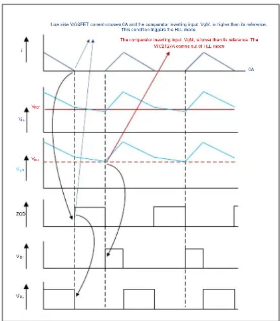
Figure 4-3 shows the control loop timing in HLL mode. The MIC2127A device has a zero crossing comparator (ZC Detection) that monitors the inductor current by sensing the voltage drop across the low-side MOSFET during its ON time. The zero crossing comparator triggers whenever the low-side MOSFET current goes negative and turns off the low-side MOSFET. The switching instant of the high-side MOSFET depends on the error amplifier output, which is same as the comparator inverting input (see the Functional Block Diagram). If the error amplifier output is higher than the comparator reference, then the MIC2127A enters into Sleep mode. During Sleep mode, both the high-side and low-side MOSFETs are kept off and the efficiency is optimized by shutting down all the nonessential circuits inside the MIC2127A. The load current is supplied by the output capacitor during Sleep mode. The control circuitry wakes up when the error amplifier output falls below the comparator reference and a t_ON pulse is triggered.
line
| Waveform | Current (i) | Voltage (V) | |----------|-------------|-------------| | GA | High | Low | | Vccr | Low | High | | Vccs | Low | Medium | | Vccd | Low | Low | | Vccd+ | Low | Low |FIGURE 4-3: MIC2127A Control Loop Timing (HLL Mode).
The typical no-load supply current during HLL mode is only about 300 A, allowing the MIC2127A device to achieve high efficiency at light load operation.
4.3 Current Limit (I LIM)
The MIC2127A device uses the low-side MOSFET R_DS(ON) to sense inductor current. In each switching cycle of the MIC2127A converter, the inductor current is sensed by monitoring the voltage across the low-side MOSFET during the OFF period of the switching cycle, during which low-side MOSFET is ON. An internal current source of 100 A generates a voltage across the external current limit setting resistor R_CL as shown in Figure 4-4.

flowchart
graph TD
    A["Current Limit Detection"] --> B["Control Logic"]
    B --> C["MIC2127A"]
    C --> D["DH"]
    C --> E["SW"]
    C --> F["DL"]
    C --> G["Rux"]
    C --> H["Iux"]
    D --> I["Vdc"]
    E --> J["L1"]
    F --> K["Rca"]
    G --> L["Ground"]
    H --> M["Ground"]
FIGURE 4-4: MIC2127A Current Limiting Circuit.
The I_LIM pin voltage ( V_ILIM ) is the difference of the voltage across the low-side MOSFET and the voltage across the resistor ( V_RCL ). The sensed voltage V_ILIM is compared with the power ground ( P_GND ) after a blanking time of 150 ns.
If the absolute value of the voltage drop across the low-side MOSFET is greater than the absolute value of the voltage across the current setting resistor ( V_RCL ), the MIC2127A triggers the current limit event. Consecutive eight-current limit events trigger the Hiccup mode. Once the controller enters into Hiccup mode, it initiates a soft start sequence after a hiccup timeout of 4 ms (typical). Both the high-side and low-side MOSFETs are turned off during hiccup timeout. The hiccup sequence, including the soft start, reduces the stress on the switching FETs and protects the load and supply from severe short conditions.
The current limit can be programmed by using the following Equation 4-4.
EQUATION 4-4:
$$ R _ {C L} = \frac {\left(I _ {C L I M} \quad \frac {\Delta I L _ {P P}}{2}\right) + \times R _ {D S O N (} + V _ {O F F S E T}}{I _ {C L}} $$
Where:
$$ I _ {C L I M} = \text { Load current limit } $$
$$ R _ {D S (O N)} = \text { On - resistance of low - side power MOSFET } $$
$$ \Delta I L _ {P P} = \text { Inductor peak - to - peak ripple current } $$
$$ V _ {\text { OFFSET }} = \text { Current - limit comparator offset } (1 5 \mathrm{mV} \max.) $$
$$ I _ {C L} = \text { Current - limit source current } (1 0 0 \mu \text { A typ }) $$
Since MOSFET R_DS(ON) varies from 30%-40% with temperature, it is recommended to consider the R_DS(ON) variation while calculating R_CL in the above equation, to avoid false current limiting due to increased MOSFET junction temperature rise. Also connect the SW pin directly to the drain of the low-side MOSFET to accurately sense the MOSFETs R_DS(ON) .
To improve the current limit variation, the MIC2127A adjusts the internal source current of the current limit ( I_CL ) at a rate of 0.3 A/ ^ C when the MIC2127A junction temperature changes to compensate the R_DS(ON) variation of external low-side MOSFET. The effectiveness of this method depends on the thermal gradient between the MIC2127A and the external low-side MOSFET. The lower the thermal gradient, the better the current limit variation.
A small capacitor ( C_CL ) can be connected from the I_LIM pin to P_GND to filter the switch node ringing during the OFF time, allowing a better current sensing. The time constant of R_CL and C_CL should be less than the minimum OFF time.
4.4 Negative Current Limit
The MIC2127A device implements negative current limit by sensing the SW voltage when the low-side FET is ON. If the SW node voltage exceeds 48 mV typical, the device turns off the low-side FET for 500 ns. Negative current limit value is shown in Equation 4-5.
EQUATION 4-5:
$$ I _ {N L I M} = \frac {4 8 m V}{R _ {D S O N (\quad)}} $$
Where:
$$ I _ {N L I M} = \text { Negative current limit } $$
$$ R _ {D S (O N)} = \text { On - resistance of low - side power MOSFET } $$
4.5 High-Side MOSFET Gate Drive (DH)
The MIC2127A's high-side drive circuit is designed to switch an N-Channel external MOSFET. The MIC2127A Functional Block Diagram shows a
bootstrap diode between the P_VDD and BST pins. This circuit supplies energy to the high-side drive circuit. A low ESR ceramic capacitor should be connected between BST and SW pins (refer to the Typical Application Circuit circuit). The capacitor between BST and SW pins, C_BST , is charged while the low-side MOSFET is on. When the high-side MOSFET driver is turned on, energy from C_BST is used to turn the MOSFET on. A minimum of 0.1 F low ESR ceramic capacitor is recommended between BST and SW pins. The required value of C_BST can be calculated using the following Equation 4-6:
EQUATION 4-6:
$$ C _ {B S T} = \frac {Q _ {G - I H S}}{\Delta V _ {C B S T}} $$
Where:
$$ \mathrm{Q} _ {\text { G_HS }} = \text { High - side MOSFET total gate charge } $$
$$ \begin{array}{r l} \Delta V _ {C B S T} & = \text { Voltage drop across the } C _ {B S T}, \ & \text { generally } 5 0 \mathrm{mV} \text { to } 1 0 0 \mathrm{mV} \end{array} $$
A small resistor in series with C_BST can be used to slow down the turn-on time of the high-side N-channel MOSFET.
4.6 Low-Side MOSFET Gate Drive (DL)
MIC2127A's low-side drive circuit is designed to switch an N-Channel external MOSFET. The internal low-side MOSFET driver is powered by P_VDD . Connect a minimum of 4.7 F low-ESR ceramic capacitor to supply the transient gate current of the external MOSFET.
4.7 Auxiliary Bootstrap LDO (EXTVDD)
MIC2127A features an auxiliary bootstrap LDO that improves the system efficiency by supplying the MIC2127A internal circuit bias power and gate drivers from the converter output voltage. This LDO is enabled when the voltage on the EXTVDD pin is above 4.6V (typical) and, at the same time, the main LDO that operates from V_IN is disabled to reduce power consumption. Connect EXTVDD to the output of the buck converter if it is between 4.7V and 14V. When the EXTVDD is tied to V_OUT , a voltage spike will occur at the PV_DD and V_DD during a fast hard short at V_OUT . Larger decoupling ceramic capacitors of 10 F at PV_DD and V_DD are recommended for such a situation.
5.0 APPLICATIONS INFORMATION
5.1 Setting the Switching Frequency
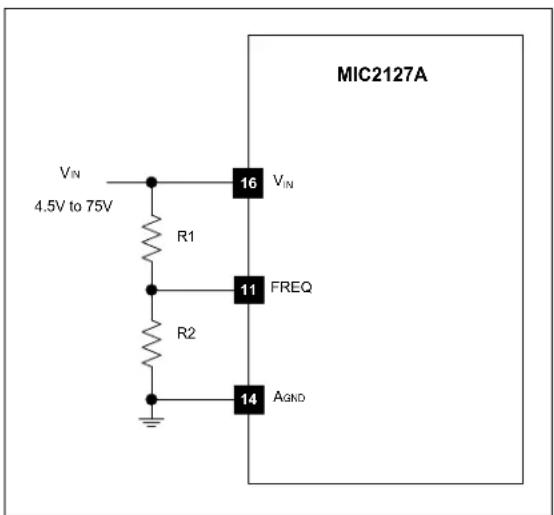
The MIC2127A device is an adjustable-frequency, synchronous buck controller, featuring a unique adaptive on-time control architecture. The switching frequency can be adjusted between 270 kHz-800 kHz by changing the resistor divider network between V_IN and A_GND pins consisting of R_1 and R_2 , as shown in Figure 5-1.
text_image
MIC2127A VIN 4.5V to 75V R1 16 VIN 11 FREQ R2 14 AGNDFIGURE 5-1: Switching Frequency Adjustment.
Equation 5-1 shows the estimated switching frequency.
EQUATION 5-1:
$$ f _ {S W _ A D J} = f _ {O} \times \frac {R _ {2}}{R _ {1} + R _ {2}} $$
f_O is the switching frequency when R_1 is 100 kΩ and R_2 being open; f_O is typically 800 kHz. For more precise setting, it is recommended to use Figure 5-2.

line
| R₂ (kΩ) | Switching Frequency (kHz) - V_IN = 24V | Switching Frequency (kHz) - V_IN = 75V | Switching Frequency (kHz) - V_IN = 48V | | ------- | ------------------------------------- | -------------------------------------- | -------------------------------------- | | 50 | ~250 | ~250 | ~250 | | 500 | ~550 | ~600 | ~650 | | 5000 | ~650 | ~700 | ~720 |FIGURE 5-2: Switching Frequency vs. R
5.2 Output Voltage Setting
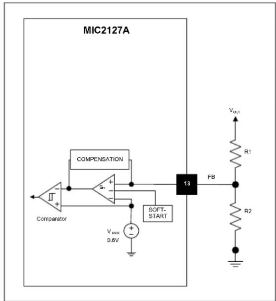
The output voltage can be adjusted using a resistor divider from output to A_GND whose mid-point is connected to the FB pin, as shown the Figure 5-3.
text_image
MIC2127A COMPENSATION g+ - Comparator VOUT R1 13 F8 SOFT- START VOUT 0.6V R2FIGURE 5-3: Output Voltage Adjustment.
The output voltage can be calculated using Equation 5-2.
EQUATION 5-2:
$$ V _ {O U T} = V _ {R E F} \times \left(1 - \frac {R _ {I}}{R _ {2}}\right) + $$
Where:
$$ V _ {R E F} = 0. 6 \mathrm{V} $$
The maximum output voltage that can be programmed using the MIC2127A is limited to 30V, if not limited by the maximum duty cycle (see Equation 4-2).
A typical value of R_1 is less than 30 kΩ. If R_1 is too large, it may allow noise to be introduced into the voltage feedback loop. It also increases the offset between the set output voltage and actual output voltage because of the error amplifier bias current. If R_1 is too small in value, it will decrease the efficiency of the power supply, especially at light loads. Once R_1 is selected, R_2 can be calculated using Equation 5-3.
EQUATION 5-3:
$$ R _ {2} = \frac {R _ {I}}{\frac {V _ {O U T}}{V _ {R E F}} I} $$
5.3 MOSFET Selection
Important parameters for MOSFET selection are:
- Voltage rating
- On-resistance
- Total gate charge
The voltage rating for the high-side and low-side MOSFETs is essentially equal to the power stage input voltage V_IN . A safety factor of 30% should be added to the V_IN(MAX) while selecting the voltage rating of the MOSFETs to account for voltage spikes due to circuit parasitic elements.
5.3.1 HIGH-SIDE MOSFET POWER LOSSES
The total power loss in the high-side MOSFET ( P_HSFET ) is the sum of the power losses because of conduction ( P_CONDUCTION ), switching ( P_SW ), reverse recovery charge of low-side MOSFET body diode ( P_Qrr ) and MOSFET's output capacitance discharge, as calculated in the Equation 5-4.
EQUATION 5-4:
| P_HSFET | P_CONDUCTION IIS( + )P_SW IIS( + )P_Qrr | P_COSS^± |
| P_CONDUCTION HS( = )(I_RMS HS()^2× R_DS(ON\_HS) | ||
| P_SW(IIS) = 0.5× V_IN× I_LOAD×(t_R+t_F)× f_SW | ||
| P_Qrr = V_IN× Q_rr× f_SW | ||
| P_COSS = 12×(C_OSS IIS( + )C_OSS IIS( )×(V_IN)^2× f_SW | ||
| Where: | ||
| R_DS(ON\_HS) | = | On-resistance of the high-side MOSFET |
| V_IN | = | Operating input voltage |
| I_LOAD | = | Load current |
| f_SW | = | Operating switching frequency |
| Q_rr | = | Reverse recovery charge of low-side MOSFET body diode or of external diode across low-side MOSFET |
| C_OSS(HS) | = | Effective high-side MOSFET output capacitance |
| C_OSS(LS) | = | Effective low-side MOSFET output capacitance |
| k_RMS(HS) | = | RMS current of the high-side MOSFET which can be calculated using Equation 5-5. |
| t_R, t_F | = | The high-side MOSFET turn-on and turn-off transition times which can be approximated by Equation 5-7 and Equation 5-8 |
EQUATION 5-5:
$$ I _ {R M S H S (\text { 一 })} = I _ {L O A D} \times \sqrt {D} $$
I_LOAD is the load current and D is the operating duty cycle, given by Equation 5-6.
EQUATION 5-6:
$$ D = \frac {V _ {O U T}}{V _ {I N}} $$
EQUATION 5-7:
$$ t _ {R} = \frac {Q _ {S W H S (} \times [ R _ {D H (P U L L U P)} + R _ {H S (G A T E)} ]}{V _ {D D} - V _ {T H}} $$
EQUATION 5-8:
$$ t _ {F} = \frac {Q _ {S W H S (}}{V _ {T H}} \times \left\lceil R _ {D H (\underline {{P U L L}} D O W N)} + R _ {H S (G A T E)} \right\rceil $$
Where:
| R_DH(PULL-UP) | = High-side gate driver pull-up resistance |
| R_DH(PULL-DOWN) | = High-side gate driver pull-down resistance |
| R_HS(GATE) | = High-side MOSFET gate resistance |
| V_TH | = Gate to Source threshold voltage of the high-side MOSFET |
| Q_SW(HS) | = Switching gate charge of the high-side MOSFET which can be approximated by Equation 5-9. |
EQUATION 5-9:
$$ Q _ {S W H S (} = \frac {Q _ {G S H S (}}{2} + Q _ {G D H S (}) $$
Where:
| Q_GS(HS) | = High-side MOSFET gate to source charge |
| Q_GD(HS) | = High-side MOSFET gate to drain charge |
5.3.2 LOW-SIDE MOSFET POWER LOSSES
The total power loss in the low-side MOSFET ( P_LSFET ) is the sum of the power losses because of conduction ( P_CONDUCTION(LS) ) and body diode conduction during the dead time ( P_DT ), as calculated in Equation 5-10.
EQUATION 5-10:
$$ P _ {L S F E T} \quad P _ {\text { CONDUCTION LS( ) }} + \mathcal {P} _ {D T} $$
$$ P _ {C O N D U C T I O N L S (\quad)} \left(I _ {R M S L S (\quad)}\right) ^ {2} \times \mathcal {R} _ {D S O N _ L S (\quad)} $$
$$ P _ {D T} = 2 V \times_ {F} \times I _ {L O A D} \times t _ {D T} \times f _ {S W} $$
Where:
R_DS(ON_LS) = On - resistance of the low - side MOSFET
V_F = Low-side MOSFET body diode forward voltage drop
t_DT = Dead time which is approximately 20 ns
f_SW = Switching Frequency
I_RMS(LS) = RMS current of the low-side MOSFET which can be calculated using Equation 5-11
EQUATION 5-11:
$$ I _ {R M S L S (\text { = })} I _ {L O A D} \times \sqrt {1 - D} $$
Where:
$$ I _ {\text { LOAD }} = \text { load current } $$
D = operating duty cycle
5.4 Inductor Selection
Inductance value, saturation and RMS currents are required to select the output inductor. The input and output voltages and the inductance value determine the peak-to-peak inductor ripple current.
The lower the inductance value, the higher the peak-to-peak ripple current through the inductor, which increases the core losses in the inductor. Higher inductor ripple current also requires more output capacitance to smooth out the ripple current. The greater the inductance value, the lower the peak-to-peak ripple current, which results in a larger and more expensive inductor.
A good compromise between size, loss and cost is to set the inductor ripple current to be equal to 30% of the maximum output current.
The inductance value is calculated by Equation 5-12.
EQUATION 5-12:
$$ L = \frac {V _ {O U T} \times (V _ {I N} - V _ {O U T})}{V _ {I N} \times f _ {S W} \times 0 . 3 k \times_ {F L}} $$
Where:
V_IN = Input voltage
f_SW = Switching frequency
I_FL = Full load current
V_OUT = Output voltage
For a selected Inductor, the peak-to-peak inductor current ripple can be calculated using Equation 5-13.
EQUATION 5-13:
$$ \Delta I _ {L _ P P} = \frac {V _ {O U T} \times (V _ {I N} - V _ {O U T})}{V _ {I N} \times f _ {S W} \times L} $$
The peak inductor current is equal to the load current plus one half of the peak-to-peak inductor current ripple which is shown in Equation 5-14.
EQUATION 5-14:
$$ I _ {L _ P K} = I _ {L O A D} + \frac {\Delta I _ {L _ P P}}{2} $$
The RMS and saturation current ratings of the selected inductor should be at least equal to the RMS current and saturation current calculated in Equation 5-15 and Equation 5-16.
EQUATION 5-15:
$$ I _ {L _ R M S} = \sqrt {\left(I _ {L O A D (M A X)}\right) ^ {2} + \frac {\left(\Delta I _ {L _ P P}\right) ^ {2}}{1 2}} $$
Where:
I_LOAD(MAX) = Maximum load current
EQUATION 5-16:
$$ I _ {L _ S A T} = \frac {(R _ {C L} \times I _ {C L}) + 1 5 m V}{R _ {D S (O N)}} $$
Where:
R_CL = Current limit resistor
I_CL = Current-Limit Source Current (100 A typical)
R_DS(ON) = On-resistance of low-side power MOSFET
Maximizing efficiency requires the proper selection of core material and minimizing the winding resistance. Use of ferrite materials is recommended in the higher switching frequency applications. Lower-cost iron powder cores may be used, but the increase in core loss reduces the efficiency of the power supply. This is especially noticeable at low output power. The winding resistance decreases efficiency at the higher output current levels. The winding resistance must be minimized, although this usually comes at the expense of a larger inductor. The power dissipated in the inductor is equal to the sum of the core and copper losses. At higher output loads, the core losses are usually insignificant and can be ignored. At lower output currents, the core losses can be a significant contributor. Core loss information is usually available from the magnetic's vendor.
The amount of copper loss in the inductor is calculated by Equation 5-17.
EQUATION 5-17:
$$ P _ {I N D U C T O R C U (\quad)} (I _ {L _ R M S}) ^ {2} \times R _ {D C R} $$
5.5 Output Capacitor Selection
The main parameters for selecting the output capacitor are capacitance value, voltage rating and RMS current rating. The type of the output capacitor is usually determined by its equivalent series resistance (ESR). Recommended capacitor types are ceramic, tantalum, low-ESR aluminum electrolytic, OS-CON and POSCAP. The output capacitor ESR also affects the control loop from a stability point of view. The maximum value of ESR can be calculated using Equation 5-18.
EQUATION 5-18:
$$ E S R \frac {\Delta V _ {O U T _ P P}}{\Delta I _ {L _ P P}} \leq $$
Where:
$$ \begin{array}{l} \Delta V _ {\text { OUT_PP }} = \text { Peak - to - peak output voltage ripple } \ \Delta I _ {L _ P P} = \text { Peak - to - peak inductor current ripple } \ \end{array} $$
The required output capacitance to meet steady state output voltage ripple can be calculated using Equation 5-19.
EQUATION 5-19:
$$ C _ {O U T} \quad \frac {\Delta I _ {L _ P P}}{8 f \times {} _ {S W} \times \Delta V _ {O U T _ P P}} = $$
Where:
$$ C _ {O U T} = \text { Output capacitance value } $$
$$ f _ {S W} \quad = \quad \text { Switching frequency } $$
$$ \Delta V _ {\text { OUT_PP }} = \text { Steady state output voltage ripple } $$
As described in Section 4.1 "Theory of Operation", the MIC2127A device requires at least 20mV peak-to-peak ripple at the FB pin to ensure that the g_M amplifier and the comparator behave properly. Also, the output voltage ripple should be in phase with the inductor current. Therefore, the output voltage ripple caused by the output capacitor's value should be much smaller than the ripple caused by the output capacitor ESR. If low-ESR capacitors, such as ceramic capacitors, are selected as the output capacitors, a ripple injection circuit should be used to provide enough feedback-voltage ripple. Refer to the Section 5.7 "Ripple Injection" for details.
The voltage rating of the capacitor should be twice the output voltage for tantalum and 20% greater for aluminum electrolytic, ceramic or OS-CON. The output capacitor RMS current is calculated in Equation 5-20.
EQUATION 5-20:
$$ I _ {C _ O U T (R M S)} = \frac {\Delta I _ {L P P}}{\sqrt {1 2}} $$
The power dissipated in the output capacitor is shown in Equation 5-21.
EQUATION 5-21:
$$ P _ {D I S (C _ O U T)} = (I _ {C _ O U T (R M S)}) ^ {2} \times E S R _ {C _ O U T} $$
5.6 Input Capacitor Selection
The input capacitor reduces peak current drawn from the power supply and reduces noise and voltage ripple on the input. The input voltage ripple depends on the input capacitance and ESR. The input capacitance and ESR values can be calculated using Equation 5-22.
EQUATION 5-22:
$$ C _ {I N} = \frac {I _ {L O A D} D 1 D - (\quad)}{\eta \times f _ {S W} \times \Delta V _ {I N C}} \quad \times \times $$
$$ E S R _ {C _ I N} = \frac {\Delta V _ {I N E S R}}{I _ {L P K}} $$
Where:
$$ \begin{array}{l} I _ {\text { L O A D }} = \text { L o a d C u r r e n t } \ I _ {L P K} = \text { Peak Inductor Current } \ \Delta V _ {\text { INC }} = \text { Input ripple due to capacitance } \ \Delta V _ {\text { INESR }} = \text { Input ripple due to input capacitor ESR } \ \eta = \text { Power conversion efficiency } \ \end{array} $$
The input capacitor should be rated for ripple current rating and voltage rating. The RMS value of input capacitor current is determined at the maximum output current. The RMS current rating of the input capacitor should be greater than or equal to the input capacitor RMS current calculated using Equation 5-23.
EQUATION 5-23:
$$ I _ {C _ I N (R M S)} = I _ {L O A D (M A X)} \times \sqrt {D \times (1 - D)} $$
The power dissipated in the input capacitor is calculated using Equation 5-24.
EQUATION 5-24:
$$ P _ {D I S S (C _ I N)} = \left(I _ {C _ I N (R M S)}\right) ^ {2} \times E S R _ {C _ I N} $$
5.7 Ripple Injection
The minimum recommended ripple at the FB pin for proper operation of the MIC2127A error amplifier and comparator is 20 mV. However, the output voltage ripple is generally designed as 1%-2% of the output voltage. For low output voltages, such as a 1V, the output voltage ripple is only 10 mV-20 mV, and the feedback voltage ripple is less than 20 mV. If the feedback voltage ripple is so small that the g_M amplifier and comparator cannot sense it, then the MIC2127A loses control and the output voltage is not regulated. In order to have sufficient V_FB ripple, the ripple injection method should be applied for low output voltage ripple applications.
The applications are divided into three situations according to the amount of the feedback voltage ripple:
- Enough ripple at the feedback due to the large ESR of the output capacitor (Figure 5-4). The converter is stable without any additional ripple injection at the FB node. The feedback voltage ripple is given by Equation 5-25.
EQUATION 5-25:
$$ \Delta V _ {F B (P P)} = \frac {R _ {2}}{R _ {2} + R _ {1}} \times E S R \times \Delta I _ {L _ {-} P P} $$
I_L_PP is the peak-to-peak value of the inductor current ripple.
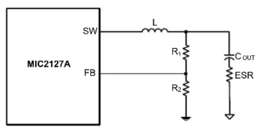
text_image
MIC2127A SW L FB R1 R2 COUT ESRFIGURE 5-4: Enough Ripple at FB.
- Inadequate ripple at the feedback voltage due to the small ESR of the output capacitor.
The output voltage ripple can be fed into the FB pin through a feed forward capacitor, C_FF in this case, as shown in Figure 5-5. The typical C_FF value is between 1 nF-100 nF. With the feed forward capacitor, the feedback voltage ripple is very close to the output voltage ripple, which is shown in Equation 5-26.
EQUATION 5-26:
$$ \Delta V _ {F B (P P)} = E S R \times \Delta I _ {L, P P} $$
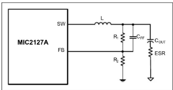
text_image
MIC2127A SW FB L R1 CFF COUT R2 ESRFIGURE 5-5: Inadequate Ripple at FB.
- Virtually no ripple at the FB pin voltage due to the very-low ESR of the output capacitors.
In this case, additional ripple can be injected into the FB pin from the switching node SW, via a resistor R_INJ and a capacitor C_INJ , as shown in Figure 5-6.
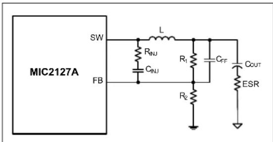
text_image
MIC2127A SW L RINJ CINJ FB R1 CFF COUT ESRFIGURE 5-6: Invisible Ripple at FB.
The injected ripple at the FB pin in this case is given by the Equation 5-27.
EQUATION 5-27:
$$ \Delta V _ {F B (P P)} = \frac {V _ {O U T} 1 D - (\quad)}{C _ {F F} \times R f _ {I N J} \times_ {S W}} \quad \times $$
In Equation 5-27, it is assumed that the time constant associated with the C_FF meets the criterion shown in Equation 5-28.
EQUATION 5-28:
$$ \tau \geq T _ {S W} $$
$$ \tau = C _ {F F} \times (R _ {1} | R _ {2} | R _ {I N J}) $$
The process of sizing the ripple injection resistor and capacitors is:
- Select C INJ in the range of 47 nF-100 nF, which can be considered as short for a wide range of the frequencies.
- Select C FF in the range of 0.47 nF-10 nF, if R 1 and R _2 are in kΩ range.
- Select R INJ according to Equation 5-29.
EQUATION 5-29:
$$ R _ {I N J} = \frac {V _ {O U T} - 1 - (D)}{C _ {F F} \times f _ {S W} \times \Delta V _ {F B (P P)}} \quad \times $$
Where:
V_OUT = Output voltage
D = Duty cycle
f_SW = Switching frequency
V_FB(PP) = Injected Feedback Ripple (20 mV to 100 mV)
Once all the ripple injection component values are calculated, ensure that the criterion shown in Equation 5-28 is met.
For high duty cycle applications with D > 40%, the procedures to design the ripple injection circuit components are as below:
- For given feedback divider resistor values, select C_FF such that the time constant formed by C_FF and feedback divider is 50% of the switching period as given in Equation 5-30:
EQUATION 5-30:
$$ C _ {F F} \times R _ {F B E Q} = 0. 5 \times T _ {S W} $$
$$ R _ {F B E Q} = R _ {1} \left| R _ {2} \right. = \frac {R _ {1} \times R _ {2}}{R _ {1} + R _ {2}} $$
- Calculate R_INJ using the Equation 5-29 Make sure that the injected ripple voltage into FB pin is in the range of 20 mV to 100 mV.
- Choose C_INJ = 100 nF or at least 10 times the C_FF value.
5.8 Power Dissipation in MIC2127A
The MIC2127A features two Low Dropout Regulators (LDOs) to supply power at the P_VDD pin from either V_IN or EXTVDD depending on the voltage at the EXTVDD pin. P_VDD powers MOSFET drivers and V_DD pin, which is recommended to connect to P_VDD through a low pass filter, powers the internal circuitry. In the applications where the output voltage is 5V and above (up to 14V), it is recommended to connect EXTVDD to the output to reduce the power dissipation in the MIC2127A, to reduce the MIC2127A junction temperature and to improve the system efficiency.
The power dissipation in the MIC2127A depends on the internal LDO being in use, on the gate charge of the external MOSFETs and on the switching frequency. The power dissipation and the junction temperature of the MIC2127A can be estimated using Equations 5-31, 5-32 and 5-33.
Power dissipation in the MIC2127A when EXTVDD is not used.
EQUATION 5-31:
$$ P _ {I C} = V _ {I N} \times (I _ {S W} + I _ {Q}) $$
Power dissipation in the MIC2127A when EXTVDD is used.
EQUATION 5-32:
$$ P _ {I C} \quad V _ {E X T V D D} \quad I _ {S W} + (I _ {Q}) $$
$$ I _ {S W} \quad Q _ {G} \times f _ {S W} $$
$$ Q _ {G} = Q _ {G H S} + Q _ {G L S} $$
Where:
$$ \begin{array}{l} I _ {S W} = \text { Switching current into the } V _ {\text { IN }} \text { pin } \ I _ {Q} \quad = \text { Quiescent current } \ \begin{array}{r l} {Q _ {G}} & {= \text { Total gate charge of the external MOS- }} \ & {\text { FETs which is sum of the gate charge of }} \ & {\text { high - side MOSFET } (Q _ {G _ H S}) \text { and the }} \ & {\text { low - side MOSFET } (Q _ {G _ L S}) \text { at 5V gate to }} \ & {\text { source voltage. Gate charge information }} \ & {\text { can be obtained from the MOSFETs }} \ & {\text { datasheet. }} \end{array} \ \begin{array}{r l} \mathrm{V} _ {\text {EXTVDD}} & = \text {Voltage at the EXTVDD pin} \ & (4. 6 \leq \text {EXTVDD} \leq 1 4 \mathrm{Vtyp.}) \end{array} \ \end{array} $$
The junction temperature of the MIC2127A can be estimated using Equation 5-33.
EQUATION 5-33:
$$ T _ {J} = P _ {I C} \times (\theta_ {J A} + _ {A}) T $$
Where:
$$ \begin{array}{l} T _ {J} = \text { Junction temperature } \ P _ {I C} = \text { Power dissipation } \ \theta_ {\mathrm{JA}} = \text { Junction Ambient Thermal resistance } (5 0. 8 ^ {\circ} \mathrm{C/W}) \ \end{array} $$
The maximum recommended operating junction temperature for the MIC2127A is +125°C.
Using the output voltage of the same switching regulator, when it is between 4.6V (typ.) to 14V, as the voltage at the EXTVDD pin significantly reduces the power dissipation inside the MIC2127A. This reduces the junction temperature rise as illustrated in Equation 5-35.
For the typical case of V_VIN = 48 V , O_UT = 5 V , maximum ambient temperature of +85^ and 10 mA of I_SW , the MIC2127A junction temperature when the EXTVDD is not used is given by Equation 5-34.
EQUATION 5-34:
$$ P _ {I C} = 4 8 V \times (1 0 m A + \dot {1}. 5 m A) $$
$$ P _ {I C} = 0. 5 5 2 W $$
$$ T _ {J} = (0. 5 5 2 W \times 5 0. 8 ^ {\circ} C / W) + 8 5 ^ {\circ} C $$
$$ T _ {J} = 1 1 3 ^ {\circ} C $$
When the 5V output is used as the input to the EXTVDD pin, the MIC2127A junction temperature reduces from +113°C to +88°C, as calculated in Equation 5-35.
EQUATION 5-35:
$$ P _ {I C} = 5 V \times (1 0 m A + 1. 5 m A) $$
$$ P _ {I C} = 0. 0 5 8 W $$
$$ T _ {J} = (0. 0 5 8 W \times 5 0. 8 ^ {\circ} C / W) + 8 5 ^ {\circ} C $$
$$ T _ {J} = 8 8 ^ {\circ} C $$
6.0 PCB LAYOUT GUIDELINES
The PCB layout is critical to achieve reliable, stable and efficient performance. The following guidelines should be followed to ensure proper operation of the MIC2127A converter.
6.1 IC
- The ceramic bypass capacitors, which are connected to the V_DD and P_VDD pins, must be located right at the IC. Use wide traces to connect to the V_DD , P_VDD and A_GND , and P_GND pins respectively.
- The signal ground pin (A GND) must be connected directly to the ground planes.
- Place the IC close to the point-of-load (POL).
- Signal and power grounds should be kept separate and connected at only one location.
6.2 Input Capacitor
- Place the input ceramic capacitors as closely as possible to the MOSFETs.
- Place several vias to the ground plane closely to the input capacitor ground terminal.
6.3 Inductor
- Keep the inductor connection to the switch node (SW) short.
- Do not route any digital lines underneath or close to the inductor.
- Keep the switch node (SW) away from the feedback (FB) pin.
- The SW pin should be connected directly to the drain of the low-side MOSFET to accurately sense the voltage across the low-side MOSFET.
6.4 Output Capacitor
- Use a copper plane to connect the output capacitor ground terminal to the input capacitor ground terminal.
- The feedback trace should be separate from the power trace and connected as closely as possible to the output capacitor. Sensing a long high-current load trace can degrade the DC load regulation.
6.5 MOSFETs
- MOSFET gate drive traces must be short and wide. The ground plane should be the connection between the MOSFET source and P_GND .
- Chose a low-side MOSFET with a high C_GS / C_GD ratio and a low internal gate resistance to minimize the effect of dV/dt inducted turn-on.
- Use a 4.5V V _GS rated MOSFET. Its higher gate threshold voltage is more immune to glitches than a 2.5V or 3.3V rated MOSFET.
7.0 PACKAGING INFORMATION
7.1 Package Marking Information
16-Pin VQFN (3 x 3 mm)
text_image
2127A WNNNExample

text_image
2127A 2256Legend: XX...X Product code or customer-specific information
Y Year code (last digit of calendar year)
YY Year code (last 2 digits of calendar year)
WW Week code (week of January 1 is week '01')
NNN Alphanumeric traceability code
eBb-free JEDEC ^® designator for Matte Tin (Sn)
* This package is Pb-free. The Pb-free JEDEC designator (e3) can be found on the outer packaging for this package.
•, ▲, ▼ Pin one index is identified by a dot, delta up, or delta down (triangle mark).
Note: In the event the full Microchip part number cannot be marked on one line, it will be carried over to the next line, thus limiting the number of available characters for customer-specific information. Package may or may not include the corporate logo.
Underbar (_) and/or Overbar (̄) symbol may not be to scale.
TITLE
16 LEAD QFN 3x3mm PACKAGE OUTLINE & RECOMMENDED LAND PATTERN

| DRAWING # | QFN33-16LD-PL-3 | UNIT | MM |
| Lead Frame | NiPdAu | Lead Finish | NiPdAu |
NOTE:
- MAX PACKAGE WARPAGE IS 0.05mm.
- MAX ALLOWABLE BURR IS 0.076mm IN ALL DIRECTIONS
- PIN #1 IS ON TOP WILL BE LASER MARKED.
- RED CIRCLE IN LAND PATTERN INDICATES THERMAL VIA. SIZE SHOULD BE 0.30-0.35mm IN DIAMETER AND SHOULD BE
CONNECTED TO GND FOR MAX THERMAL PERFORMANCE - GREEN RECTANGLES (SHADED AREA) Indicate SOLDER STENCIL OPENING ON EXPOSED PAD AREA. SIZE SHOULD BE
0.60x0.60mm IN SIZE, 0.20mm SPACING.
APPENDIX A: REVISION HISTORY
Revision F (April 2020)
The following is the list of modifications:
- Updated content in the Features section.
- Updated the Typical Application Circuit.
- Updated content in the Electrical Characteristics table.
- Updated content in Section 2.0, Typical Characteristic Curves.
- Updated content in Section 4.3, Current Limit (ILIM).
- Updated content in Section 4.5, High-Side MOSFET Gate Drive (DH).
- Updated content in Section 5.0, Applications Information.
Revision E (September 2019)
The following is the list of modifications:
- Adds AEC-Q100 qualification for new automotive option: the MIC2127AYML-TRVAO 75V Synchronous Buck Controller.
Revision D (March 2019)
The following is the list of modifications:
- Updated the I _LIM Source Current and the Zero Crossing Detection Comparator Threshold values in the Electrical Characteristics table.
Revision C (June 2018)
The following is the list of modifications:
- Updated Section 1.0 "Electrical Characteristics".
- Minor editorial corrections.
- Updated Current Limit values in Electrical Characteristics.
- Updated content in Section 3.9 "EXTVDD" and Section 4.7 "Auxiliary Bootstrap LDO (EXTVDD)".
Revision B (December 2016)
The following is the list of modifications:
- Minor editorial corrections.
- Updated the Product Identification System page.
Revision A (December 2016)
• Original release of this document.
PRODUCT IDENTIFICATION SYSTEM
To order or obtain information, e.g., on pricing or delivery, refer to the factory or the listed sales office.
PART NO. X
Device

XX
The Ground Truth image displays a single, solid horizontal line, which is a stylistic or background element (like a ruled paper line). According to Rule 2, such lines must be ignored by the OCR result. The provided OCR content is "____", which consists of underscores. Underscores are not equivalent to a solid line and are not permitted under the “Stylistic/Background Lines (Ignore)” rule. Outputting underscores for a stylistic line is incorrect because it misinterprets the line as a fill-in-the-blank placeholder. Hence, the OCR result is inconsistent with the Ground Truth.
-XX
lia Type
XXX
Qualification
Device: MIC2127A: 75V, Synchronous Buck Controller Featuring Adaptive On-Time Control
Temperature: Y
= Industrial Temperature Grade (-40°C to +125°C)
Package:
ML = 16 Lead, 3x3 mm VQFN
Media Type:
TR = 5000/reel
Qualification: Blank = Standard Part
VAO = Automotive AEC-Q100 Qualified
Examples:
a) MIC2127AYML-TR: 75V, Synchronous Buck Controller Featuring Adaptive On-Time Control, -40°C to +125°C junction temperature range, 16-LD VQFN package, 5000/reel
b) MIC2127AYML-TRVAO: 75V, Synchronous Buck Controller Featuring Adaptive On-Time Control, Automotive AEC-Q100 Qualified, -40^ to +125^ junction temperature range, 16-LD VQFN package, 5000/reel
Note the following details of the code protection feature on Microchip devices:
• Microchip products meet the specification contained in their particular Microchip Data Sheet.
- Microchip believes that its family of products is one of the most secure families of its kind on the market today, when used in the intended manner and under normal conditions.
- There are dishonest and possibly illegal methods used to breach the code protection feature. All of these methods, to our knowledge, require using the Microchip products in a manner outside the operating specifications contained in Microchip's Data Sheets. Most likely, the person doing so is engaged in theft of intellectual property.
- Microchip is willing to work with the customer who is concerned about the integrity of their code.
- Neither Microchip nor any other semiconductor manufacturer can guarantee the security of their code. Code protection does not mean that we are guaranteeing the product as "unbreakable."
Code protection is constantly evolving. We at Microchip are committed to continuously improving the code protection features of our products. Attempts to break Microchip's code protection feature may be a violation of the Digital Millennium Copyright Act. If such acts allow unauthorized access to your software or other copyrighted work, you may have a right to sue for relief under that Act.
Information contained in this publication regarding device applications and the like is provided only for your convenience and may be superseded by updates. It is your responsibility to ensure that your application meets with your specifications. MICROCHIP MAKES NO REPRESENTATIONS OR WARRANTIES OF ANY KIND WHETHER EXPRESS OR IMPLIED, WRITTEN OR ORAL, STATUTORY OR OTHERWISE, RELATED TO THE INFORMATION, INCLUDING BUT NOT LIMITED TO ITS CONDITION, QUALITY, PERFORMANCE, MERCHANTABILITY OR FITNESS FOR PURPOSE. Microchip disclaims all liability arising from this information and its use. Use of Microchip devices in life support and/or safety applications is entirely at the buyer's risk, and the buyer agrees to defend, indemnify and hold harmless Microchip from any and all damages, claims, suits, or expenses resulting from such use. No licenses are conveyed, implicitly or otherwise, under any Microchip intellectual property rights unless otherwise stated.
For information regarding Microchip's Quality Management Systems, please visit www.microchip.com/quality.
Trademarks
The Microchip name and logo, the Microchip logo, Adaptec, AnyRate, AVR, AVR logo, AVR Freaks, BesTime, BitCloud, chipKIT, chipKIT logo, CryptoMemory, CryptoRF, dsPIC, FlashFlex, flexPWR, HELDO, IGLOO, JukeBlox, KeeLoq, Kleer, LANCheck, LinkMD, maXStylus, maXTouch, MediaLB, megaAVR, Microsemi, Microsemi logo, MOST, MOST logo, MPLAB, OptoLyzer, PackeTime, PIC, picoPower, PICSTART, PIC32 logo, PolarFire, Prochip Designer, QTouch, SAM-BA, SenGenuity, SpyNIC, SST, SST Logo, SuperFlash, Symmetricom, SyncServer, Tachyon, TempTrackr, TimeSource, tinyAVR, UNI/O, Vectron, and XMEGA are registered trademarks of Microchip Technology Incorporated in the U.S.A. and other countries.
APT, ClockWorks, The Embedded Control Solutions Company, EtherSynch, FlashTec, Hyper Speed Control, HyperLight Load, IntelliMOS, Libero, motorBench, mTouch, Powermite 3, Precision Edge, ProASIC, ProASIC Plus, ProASIC Plus logo, Quiet-Wire, SmartFusion, SyncWorld, Temux, TimeCesium, TimeHub, TimePictra, TimeProvider, Vite, WinPath, and ZL are registered trademarks of Microchip Technology Incorporated in the U.S.A.
Adjacent Key Suppression, AKS, Analog-for-the-Digital Age, Any Capacitor, AnyIn, AnyOut, BlueSky, BodyCom, CodeGuard, CryptoAuthentication, CryptoAutomotive, CryptoCompanion, CryptoController, dsPICDEM, dsPICDEM.net, Dynamic Average Matching, DAM, ECAN, EtherGREEN, In-Circuit Serial Programming, ICSP, INICnet, Inter-Chip Connectivity, JitterBlocker, KleerNet, KleerNet logo, memBrain, Mindi, MiWi, MPASM, MPF, MPLAB Certified logo, MPLIB, MPLINK, MultiTRAK, NetDetach, Omniscient Code Generation, PICDEM, PICDEM.net, PICkit, PICtail, PowerSmart, PureSilicon, QMatrix, REAL ICE, Ripple Blocker, SAM-ICE, Serial Quad I/O, SMART-I.S., SQI, SuperSwitcher, SuperSwitcher II, Total Endurance, TSHARC, USBCheck, VariSense, ViewSpan, WiperLock, Wireless DNA, and ZENA are trademarks of Microchip Technology Incorporated in the U.S.A. and other countries.
SQTP is a service mark of Microchip Technology Incorporated in the U.S.A.
The Adaptec logo, Frequency on Demand, Silicon Storage Technology, and Symmcom are registered trademarks of Microchip Technology Inc. in other countries.
GestIC is a registered trademark of Microchip Technology Germany II GmbH & Co. KG, a subsidiary of Microchip Technology Inc., in other countries.
All other trademarks mentioned herein are property of their respective companies.
© 2019, Microchip Technology Incorporated, All Rights Reserved.
ISBN: 978-1-5224-5885-2
Worldwide Sales and Service
AMERICAS
Corporate Office
2355 West Chandler Blvd.
Chandler, AZ 85224-6199
Tel: 480-792-7200
Fax: 480-792-7277
Technical Support:
http://www.microchip.com/
support
Web Address:
www.microchip.com
Atlanta
Duluth, GA
Tel: 678-957-9614
Fax: 678-957-1455
Austin, TX
Tel: 512-257-3370
Boston
Westborough, MA
Tel: 774-760-0087
Fax: 774-760-0088
Chicago
Itasca, I
Tel: 630-285-0071
Fax: 630-285-0075
Dallas
Addison, TX
Tel: 972-818-7423
Fax: 972-818-2924
Detroit
Novi, MI
Tel: 248-848-4000
Houston, TX
Tel: 281-894-5983
Indianapolis
Noblesville, IN
Tel: 317-773-8323
Fax: 317-773-5453
Tel: 317-536-2380
Los Angeles
Mission Viejo, CA
Tel: 949-462-9523
Fax: 949-462-9608
Tel: 951-273-7800
Raleigh, NC
Tel: 919-844-7510
New York, NY
Tel: 631-435-6000
San Jose, CA
Tel: 408-735-9110
Tel: 408-436-4270
Canada - Toronto
Tel: 905-695-1980
Fax: 905-695-2078
ASIA/PACIFIC
Australia - Sydney
Tel: 61-2-9868-6733
China - Beijing
Tel: 86-10-8569-7000
China - Chengdu
Tel: 86-28-8665-5511
China - Chongqing
Tel: 86-23-8980-9588
China - Dongguan
Tel: 86-769-8702-9880
China - Guangzhou
Tel: 86-20-8755-8029
China - Hangzhou
Tel: 86-571-8792-8115
China - Hong Kong SAR
Tel: 852-2943-5100
China - Nanjing
Tel: 86-25-8473-2460
China - Qingdao
Tel: 86-532-8502-7355
China - Shanghai
Tel: 86-21-3326-8000
China - Shenyang
Tel: 86-24-2334-2829
China - Shenzhen
Tel: 86-755-8864-2200
China - Suzhou
Tel: 86-186-6233-1526
China - Wuhan
Tel: 86-27-5980-5300
China - Xian
Tel: 86-29-8833-7252
China - Xiamen
Tel: 86-592-2388138
China - Zhuhai
Tel: 86-756-3210040
ASIA/PACIFIC
India - Bangalore
Tel: 91-80-3090-4444
India - New Delhi
Tel: 91-11-4160-8631
India - Pune
Tel: 91-20-4121-0141
Japan - Osaka
Tel: 81-6-6152-7160
Japan - Tokyo
Tel: 81-3-6880-3770
Korea - Daegu
Tel: 82-53-744-4301
Korea - Seoul
Tel: 82-2-554-7200
Malaysia - Kuala Lumpur
Tel: 60-3-7651-7906
Malaysia - Penang
Tel: 60-4-227-8870
Philippines - Manila
Tel: 63-2-634-9065
Singapore
Tel: 65-6334-8870
Taiwan - Hsin Chu
Tel: 886-3-577-8366
Taiwan - Kaohsiung
Tel: 886-7-213-7830
Taiwan - Taipei
Tel: 886-2-2508-8600
Thailand - Bangkok
Tel: 66-2-694-1351
Tel: 43-7242-2244-39
Fax: 43-7242-2244-393
Denmark - Copenhagen
Tel: 45-4485-5910
Fax: 45-4485-2829
Finland - Espoo
Tel: 358-9-4520-820
France - Paris
Tel: 33-1-69-53-63-20
Fax: 33-1-69-30-90-79
Germany - Garching
Tel: 49-8931-9700
Germany - Haan
Tel: 49-2129-3766400
Germany - Heilbronn
Tel: 49-7131-72400
Germany - Karlsruhe
Tel: 49-721-625370
Germany - Munich
Tel: 49-89-627-144-0
Fax: 49-89-627-144-44
Germany - Rosenheim
Tel: 49-8031-354-560
Israel - Ra'anana
Tel: 972-9-744-7705
Italy - Milan
Tel: 39-0331-742611
Fax: 39-0331-466781
Italy - Padova
Tel: 39-049-7625286
Netherlands - Drunen
Tel: 31-416-690399
Fax: 31-416-690340
Norway - Trondheim
Tel: 47-7288-4388
Poland - Warsaw
Tel: 48-22-3325737
Romania - Bucharest
Tel: 40-21-407-87-50
Spain - Madrid
Tel: 34-91-708-08-90
Fax: 34-91-708-08-91
Sweden - Gothenberg
Tel: 46-31-704-60-40
Sweden - Stockholm
Tel: 46-8-5090-4654
UK - Wokingham
Tel: 44-118-921-5800
Fax: 44-118-921-5820