MCP18480 - Electronic controller Microchip - Free user manual and instructions
Find the device manual for free MCP18480 Microchip in PDF.

User questions about MCP18480 Microchip
0 question about this device. Answer the ones you know or ask your own.
Ask a new question about this device
Download the instructions for your Electronic controller in PDF format for free! Find your manual MCP18480 - Microchip and take your electronic device back in hand. On this page are published all the documents necessary for the use of your device. MCP18480 by Microchip.
USER MANUAL MCP18480 Microchip
-48V Hot Swap Controller
Features
- Allows safe board removal and insertion from a live backplane
- Accurate (<1.5%) internal voltage reference for fault detection and precision timing
- Programmable foldback current limiting
- Programmable circuit breaker current limiting
• Auto restart option for all faults - Adjustable Undervoltage lockout thresholds
- Adjustable Overvoltage protection threshold
- Adjustable Power Good delay
- Configurable Power Good output polarity
- Low-side drive of an external N-channel FET
CMOS Technology
• High-Voltage Operation
• Temperature range: Industrial (I): -40°C to +85°C
Packaging
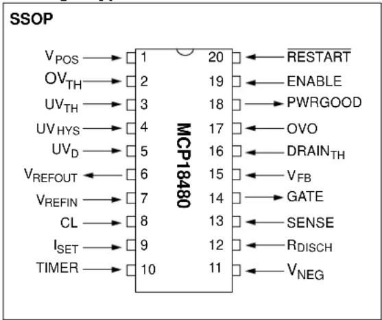
• 20-lead SSOP
Package Type
text_image
SSOP V_POS → 1 20 ← RESTART OV_TH → 2 19 ← ENABLE UV_TH → 3 18 → PWRGOOD UV_HYS → 4 17 ← OVO UV_D → 5 16 ← DRAIN_TH V_REFOUT ← 6 15 ← V_FB V_REFIN → 7 14 → GATE CL → 8 13 ← SENSE I_SET → 9 12 ← R_DISCH TIMER → 10 11 ← V_NEGDescription
The MCP18480 is a Hot Swap controller that allows boards to be safely removed or inserted from an active backplane using -48V.
When PCBs are inserted into a live backplane, high-peak or transient currents from the source are generated due to the charging of the bypass capacitors on the supply. The high transient currents can destroy connectors and capacitors. The high inrush current can pull the input voltage BUS down and reset the system.
The MCP18480 solves this problem by controlling the slew rate of the backplane voltage to the board so that these transients are eliminated. This allows boards to be removed and inserted without causing damage to connector pins and input bulk capacitors, in addition to preventing false resets to the other boards on the backplane.
The MCP18480 can be used in applications in several areas including:
- Telecom Line Cards
- Network Switches
• Network Routers and Servers - Base Station Line Cards
- Power-Over-LAN
- Power-Over-MDI
• IP Phone Switches/Routers
• Mid-Span, Power-Over-MDI
Two forms of current limit are provided in the MCP18480. These are:
- Foldback
- Circuit breaker
The foldback current-limiting circuit uses an external sense resistor and a voltage that is proportional to the external MOSFET's drain voltage. These are used to keep the MOSFET in its Safe Operating Area (SOA).
If the device remains in current limit for a programmed time period, the external N-channel FET is turned off. The option exists to configure the device to automatically restart after a programmed time delay. A programmable catastrophic current limit threshold shuts down the switch (circuit breaker) if excessive current is sensed due to a short-circuit condition.
Internal comparators are incorporated to add hysteresis for adjusting the Undervoltage Lockout (UVLO) threshold. The external N-channel MOSFET is turned on when the input is below the user-programmable, Overvoltage threshold and above the user-programmable, Undervoltage threshold.
The PWRGOOD pin indicates the status of the MCP18480 and is active when the device has completed power-up and the system is not in an Undervoltage, Overvoltage or current-limit condition.
PWRGOOD can be externally configured to either active-high or active-low to accommodate external circuitry (power supplies) that have either enabling logic.
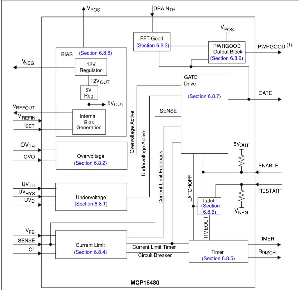
A block diagram of the MCP18480 is shown below.
MCP18480 Block Diagram
flowchart
graph TD
    A["V_NEG"] --> B["BIAS (Section 6.8.8)"]
    C["V_REFOUT"] --> D["Overvoltage (Section 6.8.2)"]
    E["V_REFIN"] --> D
    F["I_SET"] --> D
    G["OV_TH"] --> H["Undervoltage (Section 6.8.1)"]
    I["OVO"] --> H
    J["UV_TH"] --> K["Current Limit (Section 6.8.4)"]
    L["UV_HYS"] --> K
    M["UV_D"] --> K
    N["V_FB"] --> K
    O["SENSE"] --> K
    P["CL"] --> K
    Q["V_OUT"] --> R["Internal Bias Generation"]
    S["V_OUT"] --> R
    T["FET Good (Section 6.8.3)"] --> U["PWRGOOD Output Block (Section 6.8.9)"]
    V["GATE Drive (Section 6.8.7)"] --> W["Latch (Section 6.8.6)"]
    X["LATCHOFF"] --> Y["Timer (Section 6.8.5)"]
    Z["V_POS"] --> AA["DRAIN_TH"]
    AB["V_POS"] --> AC["PWRGOOD (1)"]
    AD["5VReg."] --> AE["Internal Bias Generation"]
    AF["5VOUT"] --> AE
    AG["5VOUT"] --> AE
    AH["Undervoltage Active"] --> AI["SENSSE"]
    AJ["Current Limit Feedback"] --> AK["Current Limit Timer Circuit Breaker"]
    AL["LATCHOFF"] --> AM["Latch (Section 6.8.6)"]
    AN["V_NEG"] --> AO["Timer (Section 6.8.5)"]
    AP["ENABLE"] --> AQ["5VOUT"]
    AR["RESTART"] --> AS["V_NEG"]
    AT["TIMER"] --> AU["R_DISCH"]
    AV["R_DISCH"] --> AW["TIMEOUT"]
    AX["MCP18480"] --> AY["MCP18480"]
Note 1: The PWRGOOD output pin can be either active-high or active-low. This polarity is determined by the voltage (either the level on the V_REFIN pin or level on the V_NEG pin) on the I_SET pin:
- Connecting the external R_ISET resistor to V_REFIN configures the PWRGOOD pin as active-low
- Connecting the external R_ISET resistor to V_NEG configures the PWRGOOD pin as active-high
1.0 ELECTRICAL CHARACTERISTICS
Absolute Maximum Ratings†
Ambient Temperature under bias..... -40°C to +85°C
Storage Temperature ....-65°C to +150°C
Voltage on V_POS with respect to V_NEG -0.3V to +15.0V
Voltage on DV_TH , UV_TH , V_FB , OVO and UV_HYS pins with respect to V_NEG ..... V_NEG - 0.3V to ( V_POS + 0.3V )
Voltage on V_REFIN , CL, SENSE, DRAIN TH , ENABLE and RESTART pins with respect to VNEG V _NEG - 0.3V to 6V.
Total Power Dissipation (Note 1) ....800 mW
Max. Current out of V_NEG pin.....80 mA
Max. Current into V_POS pin .....50 mA
Max. Output Current sunk by Gate pin.....80 mA
Max. Output Current sunk by V_REFOUT pin.....5 mA
Max. Output Current sunk by any other Output pin....25 mA
Max. Output Current sourced by Gate pin .....200 μA
Max. Output Current sourced by V_REFOUT pin.....5 mA
Max. Output Current sourced by any other
Output pin....25 mA
Junction to Ambient, _JA
(20 pin SSOP Package) Derating .....108.1°C/W
Junction to Case, _JC
(20 pin SSOP Package) Derating ....32.2°C/W
Lead Temperature, Soldering, 10 seconds ..... 300°C
† Notice: Stresses above those listed under "Maximum Ratings" may cause permanent damage to the device. This is a stress rating only and functional operation of the device at those or any other conditions above those indicated in the operation listings of this specification is not implied. Exposure to maximum rating conditions for extended periods may affect device reliability.
Note 1: Power Dissipation is calculated as follows:
P_DIS = V_DD × I_DD - I_OH + (V_DD - V_OH) × I_OH + (V_OL × I_OL)
DC CHARACTERISTICS
| Electrical Specifications: Unless otherwise specified, operating temperature: -40°C ≤ TA ≤ +85°C (Industrial), Supply Current: 5 mA ≤ IPOS ≤ 25 mA, R ISET = 125 kΩ, CBYP = 2 μF. | ||||||||
| Param. No. | Parameter Sym | Min | Typ | (1) | Max | Units | Conditions | |
| MD001 | Current into shunt regulator that produces VPOS output voltage that meets MD001A specification | IPOS1 | 5 | — | 25 | mA | ENABLE pin = 5V | |
| 5 | — | 25 | ENABLE pin = VNEG | |||||
| MD001A | Regulated Output Voltage Differential of VPOS to VNEG | VPOS | 10.4 | 12.0 | 13.4 | V | See MD001 | |
| MD002 | VREFOUT pin output voltage | VREFOUT | 2.463 | 2.5 | 2.538 | V | Load = 50 μA | |
| MD010 | VGATE pin output voltage | VGATE | VPOS - 2 | VPOS - 1 | VPOS | V | ||
| MD011 | Voltage on ISET pin | VISET | (VREFIN/2) - 0.02 | VREFIN/2 | (VREFIN/2) +0.02 | V | ||
| MD012A | Voltage on SENSE pin to trigger current-limiting | VSENSE | 40 | 50 | 60 | mV | VFB = VNEG | |
| MD012B | 25 | 31.0 | 40 | mV | VFB = VNEG + 0.25V | |||
| MD012C | 7 | 12 | 17 | mV | VFB = VNEG + 0.5V | |||
| MD013 | Undervoltage Threshold | UVTH | VREFIN - 0.03 | VREFIN | VREFIN + 0.03 | V | ||
| MD014A | Overvoltage Threshold | rising | OVTH | VREFIN - 0.05 | VREFIN | VREFIN + 0.05 | V | VREFIN = 2.5V |
| MD014B | falling | OVTH | VREFIN - 0.035 | VREFIN - 0.02 | VREFIN - 0.005 | V | VREFIN = 2.5V | |
| MD015 | DRAIN Pin Input Threshold Voltage | VDTH | 90 | 100 | 130 | mV | ||
Note 1: Data in the Typical ("Typ") column is based on characterization results at +25°C. This data is for design guidance only and is not tested.
2: Negative current is defined as current sourced by the pin.
3: All voltages are with respect to the V_NEG pin voltage.
DC Characteristics (Continued)
| Electrical Specification: Unless otherwise specified, operating temperature: -40^ ≤ T_A ≤ +85^ (Industrial), Supply Current: 5 mA ≤ I_POS ≤ 25 mA , R_ISET = 125 k , C_BYP = 2 F | ||||||||
| Param. No. | Parameter Sym Min Typ | (1) | Max | Units | Conditions | |||
| MD020 DRAIN pin current I | DRAIN | — — 0.1 | A DRAIN | _THpin = V_NEG | ||||
| MD021 SENSE pin current I | SENSE | — | — | 0.1 | A | |||
| MD022 GATE pin current Pu | II-up | IGATE | SENSE pin = V_NEG GATE pin = V_NEG + 4V | |||||
| MD022A | -30 | -50 | -75 | A | V_FB = V_NEG | |||
| MD022B | -9 | -17 | -33 | A | V_FB = V_NEG + 500 mV | |||
| MD022C | Pull-down | I_GATE | 31 49 | 72 | mA Any fault condition | |||
| MD023 UV _D pin current | I_UVD | -7 | -10 | -15 A UV | _TH < V_REFIN | |||
| MD024A | TIMER pin current | Pull-up | I_TIMER | -100 | -160 | -200 | A R | _ISET = 125 k , V_REFIN = 2.5V |
| MD024B | Pull-down | 52 | 78 | 104 | nA | R_ISET = 125 k , V_REFIN = 2.5V R_DISCH = 1.6 M | ||
| MD025 I | SET pin current | I_SET | V_ISET(MIN) | — | V_ISET(MAX) | A | See MD011 | |
| R_ISET(MAX) | R_ISET(MIN) | |||||||
Note 1: Data in the Typical ("Typ") column is based on characterization results at +25°C. This data is for design guidance only and is not tested.
2: Negative current is defined as current sourced by the pin.
3: All voltages are with respect to the V_NEG pin voltage.
DC Characteristics (Continued)
| Electrical Specifications: Unless otherwise specified, operating temperature: -40°C ≤ TA ≤ +85°C (Industrial), Supply Current: 5 mA ≤ IPOS ≤ 25 mA, R1SET = 125 kΩ, CBYP = 2 μF. | |||||||
| Param # | Parameter Sym Min Typ Max Units | Conditions | |||||
| MD030 Input Low Voltage V | IL | ||||||
| MD031 ENABLE pin | V | NEG | — | 0.8 | V | ||
| MD032 RESTART pin | VNEG | — | 0.8 | ||||
| MD040 Input High Voltage | V IH | ||||||
| MD041 ENABLE pin | 2.0 | — | 5.0 | V | |||
| MD042 RESTART pin | 2.0 | — | 5.0 | V | |||
| MD050 Internal Resistance on UV HYS pin | RUVHYS | 500 | 1200 | 2100 | Ω | V_UVTH < V_REFIN, I_UVHYS = 30 A | |
| 50 | 100 | — | MΩ | V_UVTH > V_REFIN, I_UVHYS = 30 A | |||
| MD060A | Input Leakage Current (Notes 2, 3) | IIL | -1 | — | +1 | μA | V_NEG ≤ V_PIN ≤ 11V, Pin at high-impedance |
| MD060B | OV_TH, UV_TH, V_FB, OVO and UV_HYS pins | — | — | ±1 | μA | V_NEG ≤ V_PIN ≤ 5V, Pin at hi-impedance | |
| MD070 Minimum current into ENABLE pin to disable MCP18480 | IEN | — | 10 | 30 | μA | I_POS = 5 mA, ENABLE = 0.8V | |
| MD080 | Output Low Voltage PWRGOOD pin | VOL | 0 | — | 0.4 | V | I_OL = 5 mA |
| MD090 | Output High Voltage PWRGOOD pin | VOH | 0.8 VPOS | —0.96 VPOS | VPOS | V | I_OH = 2 mA, 7 mA ≤ I_POS ≤ 12 mA |
| MD100 Offset Voltage at the internal comparator input that is connected to the CL pin. | VCL | -15 | — | +15 | mV | V_FB = 0 | |
Note 1: All voltages are with respect to the V_NEG pin voltage.
2: The leakage currents on the ENABLE and RESTART pins are strongly dependent on the applied voltage level. The specified levels represent normal operating conditions. Higher leakage current may be measured at different input voltages.
3: Negative current is defined as coming out of the pin.
1.1 Timing Parameter Symbology and Load Conditions
The timing parameter symbols have been created using one of the following formats:
1.1.1 TIMING CONDITIONS
The temperature and voltages specified in Table 1-2 apply to all timing specifications, unless otherwise noted. Figure 1-1 specifies the load conditions for the timing specifications.
TABLE 1-1: SYMBOLOGY
1. TppS2ppS 2. TppS
| TF Frequency T TimeE Error |
Lowercase letters (pp) indicate the device pin.
Uppercase letters and their meanings:
| S | |||||||||
| F | F | a | I | I | P | Rise | P | e | r |
| FR Fast Ramp | R | ||||||||
| H | High | V | Valid | ||||||
| I | Invalid (Hi-impedance) | Z | Hi-impedance | ||||||
| L | Low | ||||||||
TABLE 1-2: AC TEMPERATURE AND VOLTAGE SPECIFICATIONS
| AC CHARACTERISTICS | Standard Operating Conditions (unless otherwise stated)Operating temperature: -40^ ≤ T_A ≤ +85^ (industrial)Operating voltage VDD range as described in DC spec Section 1.0. |
text_image
GND RPOS 4 kΩ CByP1 2 μF 78V Transorb ROV1 1.74 MΩ CByP2 1.0 F RUV1 453 kΩ RUV2 30.9 kΩ CUVD 800 nF Rset 124 kΩ Fuse 10A VNEG MCP18480 RUV2 280 kΩ RUVHYS 280 kΩ RSET 680 nF Ctimer 680 nF 1 VPOS 2 OVTH 3 UVTH 4 UVHYS 5 UVD 6 VREFOUT 7 VREFIN 8 CL 9 ISET 10 TIMER 11 VNEG 24.9 kΩ SRS 5V RPG3 680Ω RPG4 36 kΩ QPG1 MPSA43 QPG2 2N5400 RPG5 36 kΩ QPG3 NTE261 RPG6 1500Ω RDISCH 1.6 MΩ RPG2 7.5 kΩ RSENSE 0.01Ω C1 100 nF RG1 10Ω RGD 18 kΩ CGD 3.3 nF M1 NTE2388 RFB2 124 kΩ RFB1 1.74 MΩ RDRAIN2 115kΩ RDRAIN1 1.6 MΩ ROVO2 59 kΩ ROVO1 1.74 MΩ VIN+ VOUT+ DC/DC Converter Module ON/OFF VIN- VOUT- RBPL 51 kΩ CBYPL 100 μF 100 VFIGURE 1-1: Load Conditions for Device Timing Specifications.
1.2 Timing Diagrams and Specifications
line
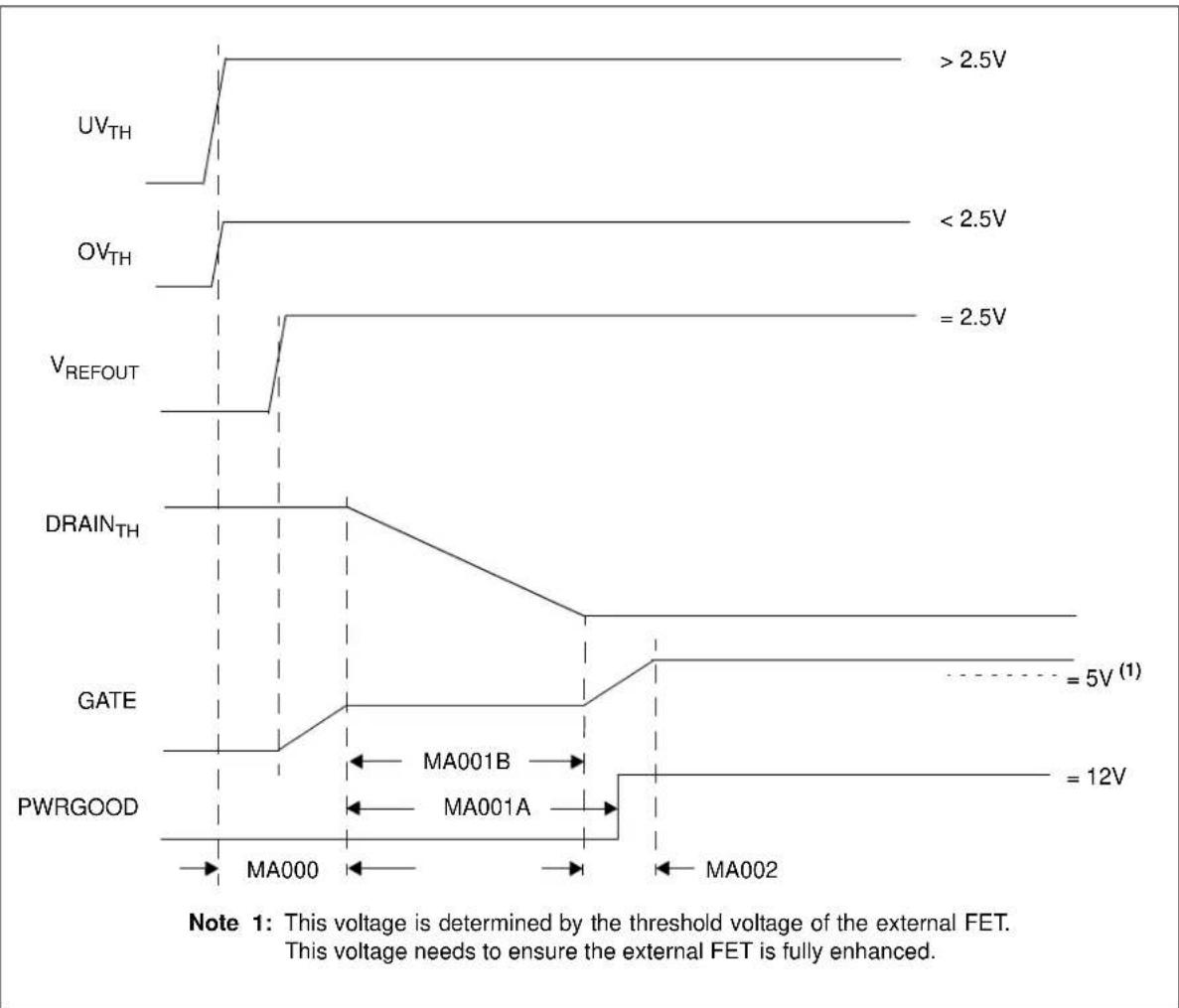
| Signal | Voltage Level | |------------|---------------| | UV_TH | >2.5V | | OV_TH | <2.5V | | V_REFOUT | =2.5V | | DRAIN_TH | - | | GATE | MA001B | | PWRGOOD | MA001A | | MA000 | - | | MA002 | - | Note 1: This voltage is determined by the threshold voltage of the external FET. This voltage needs to ensure the external FET is fully enhanced.FIGURE 1-2: Startup Waveforms.
TABLE 1-3: STARTUP TIMING REQUIREMENTS
| Param.No. | Parameter Sym Min Typ | Max Units Conditions | |||||
| MA000 UV _TH /OV _TH High (V _POS applied) to DRAIN _TH falling | T _UVOV H2 _DTH F | — | 2 | 0 | . | 2 — | |
| MA001A | DRAIN _TH falling to PWRGOOD High | T _DTH F2 _GATE PGH | — | 19.3 | — | ms | |
| MA001B | DRAIN _TH falling to GATE Fast Ramp | T _DTH F2 _GATE FR | — | 13.1 | — | ms | |
| MA002 | GATE Fast Ramp to external FET fully enhanced | T _GATE FR2FET _E | — | 16.1 | — | ms |
Note: Minimum and maximum specifications will be provided in future revisions of this data sheet.

text_image
ENABLE GATE (1) MA010 MA012 MA011Note 1: This voltage is determined by the threshold voltage of the external FET. This voltage needs to ensure the external FET is fully enhanced.
FIGURE 1-3: ENABLE-to-GATE Waveforms.
TABLE 1-4: ENABLE-TO-GATE TIMING REQUIREMENTS
| Param.No. | Parameter Sym Min Typ Max Units Conditions | ||||||
| MA010 E | NABLE Low to GATE Low T | _ENL2_GATEL | — | 23.6 | — | μs | |
| MA011 | ENABLE High to GATE Fast Ramp | T_ENH2_GATEFR | — | 41 | — | ms | |
| MA012 G | GATE Fast Ramp to GATE High T | _GATEFR2_GATEH | — | 17.8 | — | ms | |
Note: Minimum and maximum specifications will be provided in future revisions of this data sheet.
text_image
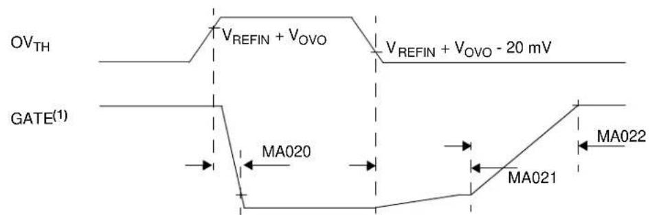
OVTH VREFIN + VOVO VREFIN + VOVO - 20 mV GATE(1) MA020 MA021 MA022Note 1: This voltage is determined by the threshold voltage of the external FET. This voltage needs to ensure the external FET is fully enhanced.
FIGURE 1-4: OV TH-to-gate Waveform.
TABLE 1-5: OV _TH -TO-GATE TIMING REQUIREMENTS
| Param.No. | Parameter Sym Min Typ Max Units Conditions | ||||||
| MA020 OV TH High to GATE Low T | _OVH2_GATEL | — | 5 | 8 | . | 4 — μ s | |
| MA021 OV TH Low to GATE Fast Ramp T | _OVL2_GATEFR | — | 40.8 | — μs | |||
| MA022 | GATE Fast Ramp to GATE High | T_GATEFR2_GATEH | — | 17.8 | — | ms | |
Note: Minimum and maximum specifications will be provided in future revisions of this data sheet.
text_image
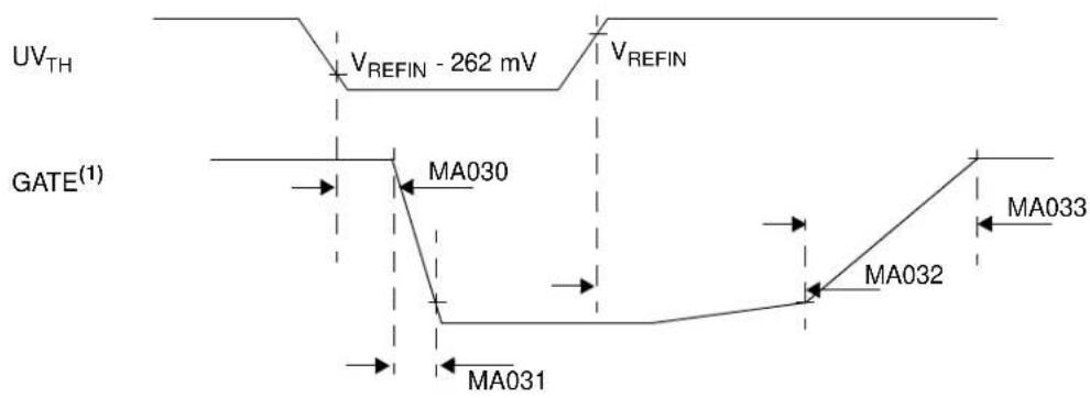
UVTH VREFIN - 262 mV VREFIN GATE(1) MA030 MA031 MA032 MA033Note 1: This voltage is determined by the threshold voltage of the external FET. This voltage needs to ensure the external FET is fully enhanced.
FIGURE 1-5: UV TH-to-gate Waveform
TABLE 1-6: UV TH-TO-GATE TIMING REQUIREMENTS
| Param.No. | Parameter Sym Min Typ | (1) | Max | Units | Conditions | ||
| MA030 U | V_TH Low to GATE Falling Edge T | _UVL2_GATEF | — | 1 | 0 | 8 | —UVD μ 800 sF C |
| MA031 | GATE High to GATE Low | T_GATEH2_GATEL | — | 25.8 | — | μs | |
| MA032 | ENABLE High to GATE Fast Ramp | T_UVH2_GATEFR | — | 40.4 | — | ms | |
| MA033 | GATE Fast Ramp to GATE High | T_GATEFR2_GATEH | — | 58.4 | — | ms | |
Note 1: Data in the Typical ("Typ") column is at 5V, 25°C, unless otherwise stated.
2: Minimum and maximum specifications will be provided in future revisions of this data sheet.
Foldback Current-Limiting
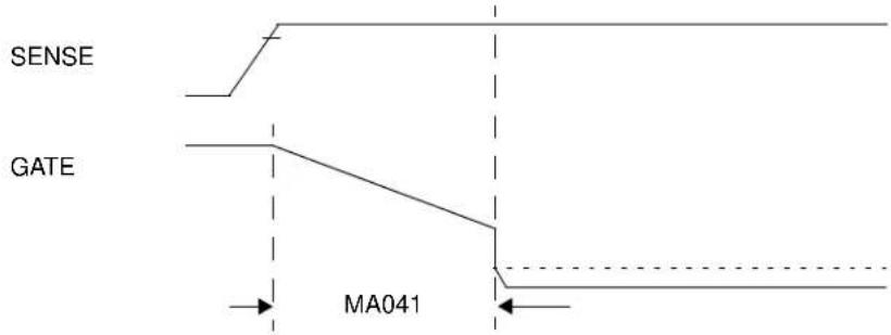
text_image
SENSE GATE MA041Recovery from Foldback Current-Limiting

text_image
SENSE GATE MA042Circuit Breaker Current-Limiting

text_image
SENSE GATE MA043FIGURE 1-6: Sense-to-gate Waveform.
TABLE 1-7: SENSE-TO-GATE TIMING REQUIREMENTS
| Param.No. | Parameter Sym Min Typ Max Units Conditions | ||||||
| MA041 GATE Current Limit to GATE Off T | _GATECL2_GATEO | — | 5 | 5 | — | _TIMER = 0.68 F R_ISET = 124 k | |
| MA042 GATE Current Limit Recovery | T_GATECL | — | 10.2 | — | ms | C_TIMER = 0.68 F R_ISET = 124 k | |
| MA043 SENSE High to GATE Off | T_SENSEH2_GATEO | — | 3 | 6 | — | m s | |
Note: Minimum and maximum specifications will be provided in future revisions of this data sheet.
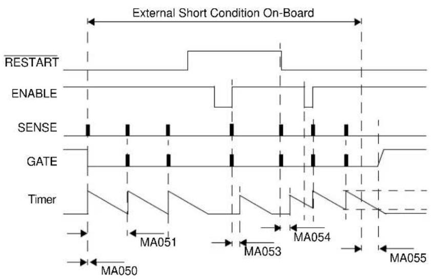
text_image
External Short Condition On-Board RESTART ENABLE SENSE GATE Timer MA051 MA053 MA054 MA055 MA050FIGURE 1-7: Current Limit Waveform.
TABLE 1-8: CURRENT LIMIT TIMING REQUIREMENTS
| Param.No. | Parameter Sym Min Typ Max Units Conditions | ||||||
| MA050 External Short to Timer period start T | SHORT2TIMERS | — | 1 | 7 | 1 | — m S | |
| MA051 Timer period | TTIMERP | — | 5.8 | — | sec | C_TIMER = 0.68 F R_DISCH = 1.6 M | |
| MA053 ENABLE High to Timer period start | T ENABLEH2TIMERS | — | 30.5 | — | mS | C_TIMER = 0.68 F R_DISCH = 1.6 M | |
| MA054 RESTART Low to Timer periodstart | TRESTARTL2TIMERS | — | 30.9 | — | mS | C_TIMER = 0.68 F R_DISCH = 11.6 M | |
| MA055 External Short removed to Timer offNote 2 | TNOSHORT2TIMERO | — | 5.8 | — | sec | C_TIMER = 0.68 F R_DISCH = 1.6 M | |
Note 1: Minimum and maximum specifications will be provided in future revisions of this data sheet.
2: This is up to one additional timer period because the external short circuit is removed asynchronously to the timer. The timer must time out before normal operation returns.
NOTES:
2.0 DC CHARACTERISTIC CURVES
Note: The graphs and tables provided following this note are a statistical summary based on a limited number of samples and are provided for informational purposes only. The performance characteristics listed herein are not tested or guaranteed. In some graphs or tables, the data presented may be outside the specified operating range (e.g., outside specified power supply range) and therefore outside the warranted range.

line
| Supply Current, I_POS (mA) | Supply Voltage, V_POS (V) | | -------------------------- | ------------------------- | | 3.0 | 11.400 | | 4.0 | 11.450 | | 5.0 | 11.500 | | 6.0 | 11.550 | | 7.0 | 11.600 | | 8.0 | 11.650 | | 9.0 | 11.700 | | 10.0 | 11.750 |Data taken with the minimum following conditions:
$$ V _ {R E F I N} = 2. 5 V, I _ {S E T} = 1 0 \mu A $$
FIGURE 2-1: Supply Current (I POS) vs. Supply Voltage (VPOS).

line
| Temperature (°C) | Supply Voltage, V_pos (V) | | ---------------- | ------------------------- | | -45 | 11.68 | | -35 | 11.70 | | -25 | 11.75 | | -15 | 11.78 | | -5 | 11.80 | | 5 | 11.82 | | 15 | 11.83 | | 25 | 11.84 | | 35 | 11.85 | | 45 | 11.86 | | 55 | 11.87 | | 65 | 11.88 | | 75 | 11.89 | | 85 | 11.90 | | 95 | 11.90 | | 105 | 11.90 | | 115 | 11.90 | | 125 | 11.90 |Data taken with the minimum following conditions:
Minimum Supply Current to bring V_POS into regulation
$$ V _ {R E F I N} = 2. 5 V, I _ {S E T} = 1 0 \mu A $$
FIGURE 2-2: Minimum Supply Current vs.
Temperature.
line
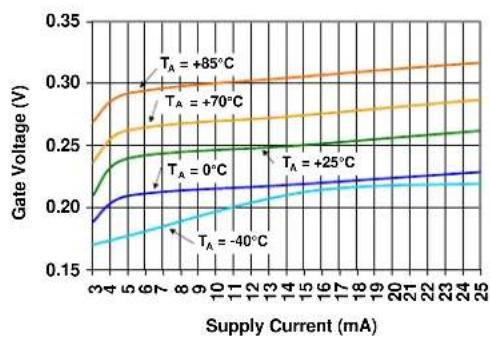
| Supply Current (mA) | TA = +85°C | TA = +70°C | TA = 0°C | TA = +25°C | TA = -40°C | | ------------------- | ---------- | ---------- | -------- | ---------- | ---------- | | 3 | 0.28 | 0.26 | 0.24 | 0.20 | 0.18 | | 4 | 0.29 | 0.27 | 0.25 | 0.21 | 0.19 | | 5 | 0.295 | 0.275 | 0.255 | 0.215 | 0.195 | | 6 | 0.298 | 0.28 | 0.26 | 0.22 | 0.20 | | 7 | 0.30 | 0.285 | 0.265 | 0.225 | 0.205 | | 8 | 0.302 | 0.29 | 0.27 | 0.23 | 0.21 | | 9 | 0.304 | 0.295 | 0.275 | 0.235 | 0.215 | | 10 | 0.306 | 0.30 | 0.28 | 0.24 | 0.22 | | 11 | 0.308 | 0.305 | 0.285 | 0.245 | 0.225 | | 12 | 0.31 | 0.31 | 0.29 | 0.25 | 0.23 | | 13 | 0.312 | 0.315 | 0.295 | 0.255 | 0.235 | | 14 | 0.314 | 0.32 | 0.30 | 0.26 | 0.24 | | 15 | 0.316 | 0.325 | 0.305 | 0.265 | 0.245 | | 16 | 0.318 | 0.33 | 0.31 | 0.27 | 0.25 | | 17 | 0.32 | 0.335 | 0.315 | 0.275 | 0.255 | | 18 | 0.322 | 0.34 | 0.32 | 0.28 | 0.26 | | 19 | 0.324 | 0.345 | 0.325 | 0.285 | 0.265 | | 20 | 0.326 | 0.35 | 0.33 | 0.29 | 0.27 | | 21 | 0.328 | 0.355 | 0.335 | 0.295 | 0.275 | | 22 | 0.33 | 0.36 | 0.34 | 0.30 | 0.28 | | 23 | 0.332 | 0.365 | 0.345 | 0.305 | 0.285 | | 24 | 0.334 | 0.37 | 0.35 | 0.31 | 0.29 | | 25 | 0.336 | 0.375 | 0.355 | 0.315 | 0.295 |Data taken with the minimum following conditions:
$$ 3 \mathrm{mA} \leq b _ {\mathrm{OS}} \leq 3 0 \mathrm{mA} $$
$$ V _ {R E F I N} = 2. 5 \mathrm{V}, I _ {S E T} = 1 0 \mu \mathrm{A} $$
Note 1:
$$ V _ {U V T H} > V _ {V R E F I N} $$
$$ V _ {O V T H} < V _ {V R E F I N} $$
$$ V _ {S E N S E} = V _ {V N E G} $$
$$ V _ {V F B} = V _ {V N E G} $$
$$ V _ {D R A I N T H} = V _ {V N E G} $$
$$ V _ {O V O} = V _ {V N E G} $$
$$ V _ {C L} = V _ {V R E F I N} $$
$$ V _ {E N A B L E} = 5 V (\text { open }) $$
$$ V _ {\text { RESTART }} = V _ {\text { VNEG }} (\text { open }) $$
FIGURE 2-3: GATE Output High-Voltage ( V_POS - V_GATE ) vs. Supply Current ( I_POS ).
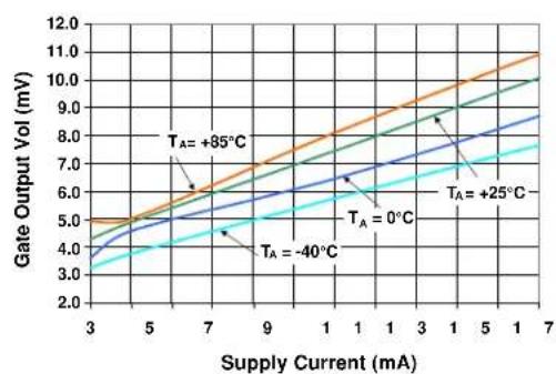
line
| Supply Current (mA) | TA = +85°C | TA = 0°C | TA = +25°C | TA = -40°C | | ------------------- | ---------- | -------- | ---------- | ---------- | | 3 | 5.0 | 4.0 | 3.5 | 3.0 | | 5 | 6.0 | 5.0 | 4.5 | 4.0 | | 7 | 7.0 | 6.0 | 5.5 | 5.0 | | 9 | 8.0 | 7.0 | 6.5 | 6.0 | | 1 | 9.0 | 8.0 | 7.5 | 7.0 | | 1.5 | 10.0 | 9.0 | 8.5 | 8.0 | | 3 | 11.0 | 10.0 | 9.5 | 9.0 | | 5 | 12.0 | 11.0 | 10.5 | 10.0 | | 7 | 13.0 | 12.0 | 11.5 | 11.0 |Data taken with the minimum following conditions:
$$ 3 \mathrm{mA} \leq b _ {\mathrm{OS}} \leq 3 0 \mathrm{mA} $$
$$ V _ {R E F I N} = 2. 5 V, I _ {S E T} = 1 0 \mu A $$
Note 1:
$$ V _ {U V T H} > V _ {V R E F I N} $$
$$ V _ {O V T H} < V _ {V R E F I N} $$
$$ V _ {S E N S E} = V _ {V N E G} $$
$$ V _ {V F B} = V _ {V N E G} $$
$$ V _ {D R A I N T H} = V _ {V N E G} $$
$$ V _ {O V O} = V _ {V N E G} $$
$$ V _ {C L} = V _ {V R E F I N} $$
$$ V _ {E N A B L E} = V _ {V N E G} $$
$$ V _ {\text { R E S T A R T }} = V _ {\text { V N E G }} (\text { o p e n }) $$
FIGURE 2-4: GATE Output Low-Voltage ( V_GATE - V_NEG ) vs. Supply Current ( I_POS ).

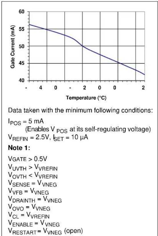
Data taken with the minimum following conditions:
$$ I _ {P O S} = 5 \mathrm{mA} $$
(Enables V_POS at its self-regulating voltage)
$$ V _ {R E F I N} = 2. 5 V, I _ {S E T} = 1 0 \mu A $$
Note 1:
$$ V _ {U V T H} > V _ {V R E F I N} $$
$$ V _ {O V T H} < V _ {V R E F I N} $$
$$ V _ {S E N S E} = V _ {V N E G} $$
$$ V _ {V F B} = V _ {V N E G} $$
$$ V _ {D R A I N T H} = V _ {V N E G} $$
$$ V _ {O V O} = V _ {V N E G} $$
$$ V _ {C L} = V _ {V R E F I N} $$
$$ V _ {E N A B L E} = 5 V (\text { open }) $$
FIGURE 2-5: GATE Source (Pull-Up)
Current vs. Temperature.
Data taken with the minimum following conditions:
$$ I _ {P O S} = 5 \mathrm{mA} $$
(Enables V POS at its self-regulating voltage)
$$ V _ {R E F I N} = 2. 5 V, I _ {S E T} = 1 0 \mu A $$
Note 1:
$$ V _ {G A T E} > 0. 5 V $$
$$ V _ {U V T H} > V _ {V R E F I N} $$
$$ V _ {O V T H} < V _ {V R E F I N} $$
$$ V _ {S E N S E} = V _ {V N E G} $$
$$ V _ {V F B} = V _ {V N E G} $$
$$ V _ {D R A I N T H} = V _ {V N E G} $$
$$ V _ {O V O} = V _ {V N E G} $$
$$ V _ {C L} = V _ {V R E F I N} $$
$$ V _ {E N A B L E} = V _ {V N E G} $$
$$ V _ {\text { R E S T A R T }} = V _ {\text { V N E G }} (\text { o p e n }) $$
FIGURE 2-6: GATE Sink (Pull-Down)
Current vs. Temperature.
line
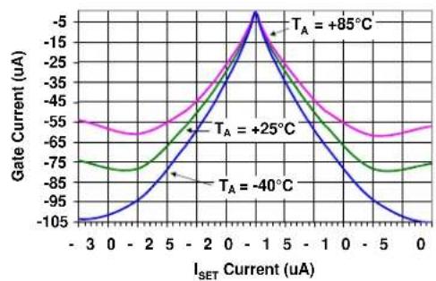
| I_SET Current (uA) | Gate Current (uA) for T_A = +85°C | Gate Current (uA) for T_A = +25°C | Gate Current (uA) for T_A = -40°C | | ------------------ | --------------------------------- | --------------------------------- | --------------------------------- | | -3 | -105 | -75 | -75 | | 0 | -5 | -55 | -75 | | 2 | -10 | -65 | -75 | | 5 | -5 | -55 | -75 | | 0 | -10 | -65 | -75 | | 2 | -5 | -55 | -75 | | 5 | -10 | -65 | -75 | | 0 | -10 | -75 | -75 |Data taken with the minimum following conditions:
$$ - 5 0 \mu A \mu A < I _ {I S E T} < 5 0 \mu A (I _ {I S E T} \neq 0) $$
$$ I _ {P O S} = 5 \mathrm{mA} $$
(Enables V POS at its self-regulating voltage)
VREFIN = 2.5V
Note 1:
$$ V _ {G A T E} > 0. 5 V $$
$$ V _ {U V T H} > V _ {V R E F I N} $$
$$ V _ {O V T H} < V _ {V R E F I N} $$
$$ V _ {S E N S E} = V _ {V N E G} $$
$$ V _ {V F B} = V _ {V N E G} $$
$$ V _ {D R A I N T H} = V _ {V N E G} $$
$$ V _ {O V O} = V _ {1} $$
$$ V _ {C L} = V _ {V R E F I N} $$
$$ V _ {E N A B L E} = 5 V (\text { open }) $$
$$ V _ {\text { RESTART }} = V _ {\text { VNEG }} (\text { open }) $$
FIGURE 2-7: GATE Source Current vs. I_SET Pin Current.

line
| Temperature (°C) | PWRGOOD, V_OL (V) | | ---------------- | ----------------- | | -4 | 0.18 | | 0 | 0.19 | | 2 | 0.20 | | 2 | 0.21 | | 2 | 0.22 | | 2 | 0.23 | | 2 | 0.24 | | 2 | 0.25 |Data taken with the minimum following conditions:
$$ I _ {\text { L O A D }} = 1 \mathrm{mA} $$
$$ I _ {P O S} = 5 \mathrm{mA} $$
(Enables V_POS at its self-regulating voltage)
V_REFIN = 2.5V, I_SET = 10 A
Note 1:
$$ V _ {U V T H} > V _ {V R E F I N} $$
$$ V _ {O V T H} < V _ {V R E F I N} $$
$$ V _ {S E N S E} = V _ {V N E G} $$
$$ V _ {V F B} = V _ {V N E G} $$
$$ V _ {D R A I N T H} = V _ {V N E G} $$
$$ V _ {O V O} = V _ {V N E G} $$
$$ V _ {C L} = V _ {V R E F I N} $$
$$ V _ {E N A B L E} = 5 V (\text { open }) $$
$$ V _ {\text { R E S T A R T }} = V _ {\text { V N E G }} (\text { o p e n }) $$
FIGURE 2-8: PWRGOOD Output Low Voltage ( V_OL ) vs. Temperature.

line
| Temperature (°C) | PWRGOOD VOH (%VPOS) | | ---------------- | ------------------- | | - | 97.5 | | 2 | 96.0 |Data taken with the minimum following conditions:
$$ I _ {\text { L O A D }} = - 1 \mathrm{mA} $$
$$ I _ {P O S} = 5 \mathrm{mA} $$
(Enables V_POS at its self-regulating voltage)
$$ V _ {R E F I N} = 2. 5 V, I _ {S E T} = 1 0 \mu A $$
Note 1:
$$ V _ {U V T H} > V _ {V R E F I N} $$
$$ V _ {O V T H} < V _ {V R E F I N} $$
$$ V _ {S E N S E} = V _ {V N E G} $$
$$ V _ {V F B} = V _ {V N E G} $$
$$ V _ {D R A I N T H} = V _ {V N E G} $$
$$ V _ {O V O} = V _ {V N E G} $$
$$ V _ {C L} = V _ {V R E F I N} $$
$$ V _ {E N A B L E} = 5 V (\text { open }) $$
$$ V _ {\text { R E S T A R T }} = V _ {\text { V N E G }} (\text { o p e n }) $$
FIGURE 2-9: PWRGOOD Output High-Voltage ( V_OH ) vs. Temperature.
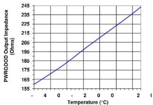
line
| Temperature (°C) | PWRGOOD Output Impedance (Ohms) | | ---------------- | ------------------------------- | | -4 | 155 | | 0 | 175 | | 2 | 195 | | 2 | 215 | | 2 | 235 | | 2 | 245 |Data taken with the minimum following conditions:
$$ I _ {P O S} = 5 \mathrm{mA} $$
(Enables V_POS at its self-regulating voltage)
$$ V _ {R E F I N} = 2. 5 V, I _ {S E T} = 1 0 \mu A $$
Note 1:
$$ V _ {U V T H} > V _ {V R E F I N} $$
$$ V _ {O V T H} < V _ {V R E F I N} $$
$$ V _ {S E N S E} = V _ {V N E G} $$
$$ V _ {V F B} = V _ {V N E G} $$
$$ V _ {D R A I N T H} = V _ {V N E G} $$
$$ V _ {O V O} = V _ {V N E G} $$
$$ V _ {C L} = V _ {V R E F I N} $$
$$ V _ {E N A B L E} = 5 V (\text { open }) $$
$$ V _ {\text { R E S T A R T }} = V _ {\text { V N E G }} (\text { o p e n }) $$
FIGURE 2-10: PWRGOOD Output High-Impedance vs. Temperature.
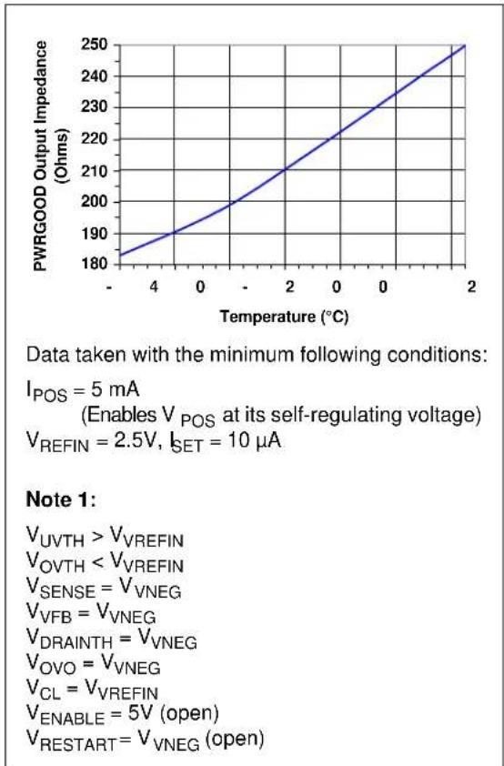
line
| Temperature (°C) | PWRGOOD Output Impedance (Ohms) | | ---------------- | ------------------------------- | | -4 | 180 | | 0 | 200 | | 2 | 210 | | 2 | 220 | | 2 | 230 | | 2 | 240 | | 2 | 250 |FIGURE 2-11: PWRGOOD Output Low-Impedance vs. Temperature.
line
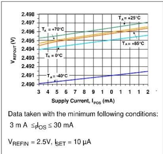
| Supply Current, I_POS (mA) | V_REFOUT (V) for T_A = +70°C | V_REFOUT (V) for T_A = +25°C | V_REFOUT (V) for T_A = +85°C | V_REFOUT (V) for T_A = -40°C | | -------------------------- | ---------------------------- | ---------------------------- | ---------------------------- | ---------------------------- | | 3 | 2.495 | 2.496 | 2.494 | 2.490 | | 5 | 2.496 | 2.497 | 2.495 | 2.491 | | 1 | 2.497 | 2.498 | 2.496 | 2.491 | | 2 | 2.497 | 2.498 | 2.496 | 2.491 |FIGURE 2-12: V REFOUT vs. Supply Current (IPOS).

line
| LOAD Current (mA) | V_REFOUT (V) for T_A = -40°C | V_REFOUT (V) for T_A = 0°C | V_REFOUT (V) for T_A = +25°C | V_REFOUT (V) for T_A = +70°C | V_REFOUT (V) for T_A = +85°C | | ----------------- | ---------------------------- | -------------------------- | ---------------------------- | ---------------------------- | ---------------------------- | | 0.25 | 2.5 | 2.5 | 2.5 | 2.5 | 2.5 | | 0.75 | 2.4 | 2.4 | 2.4 | 2.4 | 2.4 | | 1.0 | 2.3 | 2.3 | 2.3 | 2.3 | 2.3 | | 1.25 | 2.2 | 2.2 | 2.2 | 2.2 | 2.2 | | 1.5 | 2.1 | 2.1 | 2.1 | 2.1 | 2.1 | | 1.75 | 2.0 | 2.0 | 2.0 | 2.0 | 2.0 | | 2.0 | 1.9 | 1.9 | 1.9 | 1.9 | 1.9 | | 2.25 | 1.8 | 1.8 | 1.8 | 1.8 | 1.8 | | 2.5 | 1.7 | 1.7 | 1.7 | 1.7 | 1.7 | | 2.75 | 1.6 | 1.6 | 1.6 | 1.6 | 1.6 | | 3.0 | 1.5 | 1.5 | 1.5 | 1.5 | 1.5 | | 3.25 | 1.4 | 1.4 | 1.4 | 1.4 | 1.4 | | 3.5 | 1.3 | 1.3 | 1.3 | 1.3 | 1.3 | | 3.75 | 1.2 | 1.2 | 1.2 | 1.2 | 1.2 | | 4.0 | 1.1 | 1.1 | 1.1 | 1.1 | 1.1 | | 4.25 | 1.0 | 1.0 | 1.0 | 1.0 | 1.0 | | 4.5 | 0.9 | 0.9 | 0.9 | 0.9 | 0.9 | | 4.75 | 0.8 | 0.8 | 0.8 | 0.8 | 0.8 | | 5.0 | 0.7 | 0.7 | 0.7 | 0.7 | 0.7 |FIGURE 2-13: V REFOUT vs. LOAD.

line
| R_DISCH Current (uA) | T_A = +85°C | T_A = +25°C | T_A = -40°C | | --------------------- | ----------- | ----------- | ----------- | | 0 | 1.9 | 1.7 | 1.2 | | 2 | 1.95 | 1.75 | 1.25 | | 4 | 2.0 | 1.8 | 1.3 | | 6 | 2.05 | 1.85 | 1.35 | | 8 | 2.1 | 1.9 | 1.4 | | 10 | 2.1 | 1.95 | 1.45 | | 12 | 2.1 | 2.0 | 1.5 | | 14 | 2.1 | 2.0 | 1.55 | | 16 | 2.1 | 2.0 | 1.6 | | 18 | 2.1 | 2.0 | 1.65 | | 20 | 2.1 | 2.0 | 1.7 |Data taken with the minimum following conditions:
$$ - 5 0 \mu A < I _ {I S E T} < 5 0 \mu A (I _ {I S E T} \neq 0) $$
$$ I _ {P O S} = 5 \mathrm{mA} $$
(Enables V_POS at its self-regulating voltage)
$$ V _ {R E F I N} = 2. 5 V $$
Note 1:
$$ V _ {U V T H} > V _ {V R E F I N} $$
$$ V _ {O V T H} < V _ {V R E F I N} $$
$$ V _ {S E N S E} = V _ {V N E G} $$
$$ V _ {V F B} = V _ {V N E G} $$
$$ V _ {D R A I N T H} = V _ {V N E G} $$
$$ V _ {O V O} = V _ {1} $$
$$ V _ {C L} = V _ {V R E F I N} $$
$$ V _ {E N A B L E} = 5 V (\text { open }) $$
$$ V _ {\text { R E S T A R T }} = V _ {\text { V N E G }} (\text { o p e n }) $$
FIGURE 2-14: TIMER Pin Output Low Current vs. R_DISCH Current.
line
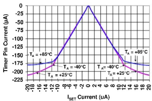
| I_SET Current (uA) | Timer Pin Current (uA) | | ------------------ | ---------------------- | | -20 | -175 | | -18 | -175 | | -16 | -175 | | -14 | -175 | | -12 | -175 | | -10 | -175 | | -8 | -125 | | -6 | -75 | | -4 | -25 | | -2 | 0 | | 0 | 0 | | 2 | 0 | | 4 | -25 | | 6 | -75 | | 8 | -125 | | 10 | -175 | | 12 | -175 | | 14 | -175 | | 16 | -175 | | 18 | -175 | | 20 | -175 |Data taken with the minimum following conditions:
$$ - 5 0 \mu A < I _ {I S E T} < 5 0 \mu A (I _ {I S E T} \neq 0) $$
$$ I _ {P O S} = 5 \mathrm{mA} $$
(Enables V POS at its self-regulating voltage)
$$ V _ {R E F I N} = 2. 5 V $$
Note 1:
$$ V _ {U V T H} > V _ {V R E F I N} $$
$$ V _ {O V T H} < V _ {V R E F I N} $$
$$ V _ {S E N S E} \geq 1 0 0 m V $$
$$ V _ {V F B} = V _ {V N E G} $$
$$ V _ {D R A I N T H} = V _ {V N E G} $$
$$ V _ {O V O} = V _ {V N E G} $$
$$ V _ {C L} = V _ {V R E F I N} $$
$$ V _ {\text { ENABLE }} = 5 V (\text { open }) $$
$$ V _ {\text { RESTART }} = V _ {\text { VNEG }} (\text { open }) $$
FIGURE 2-15: TIMER Pin Output High Current vs. I_SET Current.
line
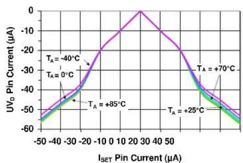
| ISET Pin Current (μA) | UVD Pin Current (μA) | | --------------------- | -------------------- | | -50 | -50 | | -40 | -40 | | -30 | -30 | | -20 | -20 | | -10 | -10 | | 0 | 0 | | 10 | -10 | | 20 | -20 | | 30 | -30 | | 40 | -40 | | 50 | -50 | | 60 | -60 |Data taken with the minimum following conditions:
$$ - 5 0 \mu A < I _ {I S E T} < 5 0 \mu A (I _ {I S E T} \neq 0) $$
$$ I _ {P O S} = 5 \mathrm{mA} $$
(Enables V_POS at its self-regulating voltage)
$$ V _ {R E F I N} = 2. 5 V $$
Note 1:
$$ V _ {U V T H} < V _ {V R E F I N} $$
$$ V _ {O V T H} < V _ {V R E F I N} $$
$$ V _ {S E N S E} = V _ {V N E G} $$
$$ V _ {V F B} = V _ {V N E G} $$
$$ V _ {D R A I N T H} = V _ {V N E G} $$
$$ V _ {O V O} = V _ {V N E G} $$
$$ V _ {C L} = V _ {V R E F I N} $$
$$ V _ {E N A B L E} = 5 V (\text { open }) $$
$$ V _ {\text { R E S T A R T }} = V _ {\text { V N E G }} (\text { o p e n }) $$
FIGURE 2-16: UV Current. D Pin Current vs. I_SET Pin
line
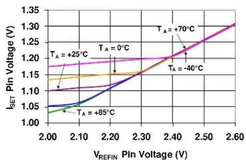
| VREFIN Pin Voltage (V) | ISET Pin Voltage (V) for TA = +25°C | ISET Pin Voltage (V) for TA = 0°C | ISET Pin Voltage (V) for TA = +70°C | ISET Pin Voltage (V) for TA = -40°C | ISET Pin Voltage (V) for TA = +85°C | | ---------------------- | ----------------------------------- | --------------------------------- | ----------------------------------- | ---------------------------------- | ----------------------------------- | | 2.00 | 1.10 | 1.15 | 1.18 | 1.14 | 1.05 | | 2.10 | 1.12 | 1.16 | 1.19 | 1.15 | 1.06 | | 2.20 | 1.14 | 1.17 | 1.20 | 1.16 | 1.07 | | 2.30 | 1.16 | 1.18 | 1.21 | 1.17 | 1.08 | | 2.40 | 1.18 | 1.19 | 1.22 | 1.18 | 1.09 | | 2.50 | 1.20 | 1.20 | 1.23 | 1.19 | 1.10 | | 2.60 | 1.22 | 1.21 | 1.24 | 1.20 | 1.11 |Data taken with the minimum following conditions:
$$ I _ {P O S} = 5 \mathrm{mA} $$
(Enables V_POS at its self-regulating voltage)
$$ \mathrm{Iset} = 1 0 \mu \mathrm{A} $$
FIGURE 2-17: I SET Pin Voltage vs. V_REFIN Pin Voltage.
line
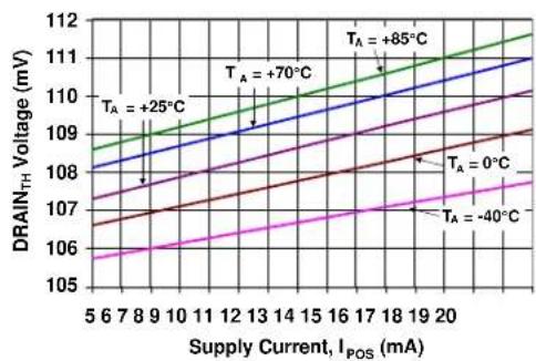
| Supply Current, I_POS (mA) | T_A = +25°C | T_A = +70°C | T_A = +85°C | T_A = 0°C | T_A = -40°C | | -------------------------- | ----------- | ----------- | ----------- | --------- | ----------- | | 5 | 108.5 | 109.0 | 109.5 | 106.5 | 105.5 | | 6 | 108.7 | 109.2 | 109.7 | 106.7 | 105.7 | | 7 | 108.9 | 109.4 | 109.9 | 106.9 | 105.9 | | 8 | 109.1 | 109.6 | 110.1 | 107.1 | 106.1 | | 9 | 109.3 | 109.8 | 110.3 | 107.3 | 106.3 | | 10 | 109.5 | 110.0 | 110.5 | 107.5 | 106.5 | | 11 | 109.7 | 110.2 | 110.7 | 107.7 | 106.7 | | 12 | 109.9 | 110.4 | 110.9 | 107.9 | 106.9 | | 13 | 110.1 | 110.6 | 111.1 | 108.1 | 107.1 | | 14 | 110.3 | 110.8 | 111.3 | 108.3 | 107.3 | | 15 | 110.5 | 111.0 | 111.5 | 108.5 | 107.5 | | 16 | 110.7 | 111.2 | 111.7 | 108.7 | 107.7 | | 17 | 110.9 | 111.4 | 111.9 | 108.9 | 107.9 | | 18 | 111.1 | 111.6 | 112.1 | 109.1 | 108.1 | | 19 | 111.3 | 111.8 | 112.3 | 109.3 | 108.3 | | 20 | 111.5 | 112.0 | 112.5 | 109.5 | 108.5 |Data taken with the minimum following conditions:
$$ 3 \mathrm{mA} \leq b _ {\mathrm{OS}} \leq 3 0 \mathrm{mA} $$
$$ V _ {R E F I N} = 2. 5 V, I _ {S E T} = 1 0 \mu A $$
Determined by PWRGOOD signal
Note 1:
$$ V _ {U V T H} > V _ {V R E F I N} $$
$$ V _ {O V T H} < V _ {V R E F I N} $$
$$ V _ {S E N S E} = V _ {V N E G} $$
$$ V _ {V F B} = V _ {V N E G} $$
$$ V _ {O V O} = V _ {V N E G} $$
$$ V _ {C L} = V _ {V R E F I N} $$
$$ V _ {E N A B L E} = 5 V (\text { open }) $$
$$ V _ {\text { R E S T A R T }} = V _ {\text { V N E G }} (\text { o p e n }) $$
FIGURE 2-18: DRAIN TH Threshold Voltage vs. Supply current ( I_POS ).

line
| Supply Current, I_POS (mA) | R_DISCH Current (nA) at T_A = -40°C | R_DISCH Current (nA) at T_A = +25°C | R_DISCH Current (nA) at T_A = +85°C | | -------------------------- | ---------------------------------- | ---------------------------------- | ---------------------------------- | | 5 | 865 | 855 | 820 | | 1 | 865 | 850 | 822 | | 0 | 865 | 850 | 823 | | 1 | 865 | 850 | 823 |Data taken with the minimum following conditions:
$$ I _ {P O S} = 5 \mathrm{mA} $$
(Enables V_POS at its self-regulating voltage)
$$ V _ {R E F I N} = 2. 5 V, I _ {S E T} = 1 0 \mu A $$
$$ R _ {D I S C H} = 1 6 \mathrm{M} \Omega $$
Note 1:
$$ V _ {U V T H} > V _ {V R E F I N} $$
$$ V _ {O V T H} < V _ {V R E F I N} $$
$$ V _ {S E N S E} = V _ {V N E G} $$
$$ V _ {V F B} = V _ {V N E G} $$
$$ V _ {D R A I N T H} = V _ {V N E G} $$
$$ V _ {O V O} = V _ {V N E G} $$
$$ V _ {C L} = V _ {V R E F I N} $$
$$ V _ {E N A B L E} = 5 V (\text { open }) $$
$$ V _ {\text { R E S T A R T }} = V _ {\text { V N E G }} (\text { o p e n }) $$
FIGURE 2-19: R Current ( I_POS ).
DISCH Current vs. Supply

line
| R_DISCH Current (uA) | R_DISCH Voltage (V) for T_A = +85°C | R_DISCH Voltage (V) for T_A = +25°C | R_DISCH Voltage (V) for T_A = -40°C | | --------------------- | ----------------------------------- | ----------------------------------- | ----------------------------------- | | 0 | 1.270 | 1.260 | 1.260 | | 5 | 1.275 | 1.265 | 1.265 | | 10 | 1.280 | 1.270 | 1.270 | | 15 | 1.285 | 1.275 | 1.275 | | 20 | 1.290 | 1.280 | 1.280 | | 25 | 1.285 | 1.285 | 1.285 | | 30 | 1.290 | 1.290 | 1.290 | | 35 | 1.285 | 1.285 | 1.285 | | 40 | 1.290 | 1.290 | 1.290 | | 45 | 1.295 | 1.295 | 1.295 | | 50 | 1.300 | 1.300 | 1.300 |Data taken with the minimum following conditions:
$$ I _ {P O S} = 5 \mathrm{mA} $$
(Enables V_POS at its self-regulating voltage)
$$ V _ {R E F I N} = 2. 5 \mathrm{V}, I _ {S E T} = 1 0 \mu \mathrm{A} $$
I_RDISCH from 100 nA to 10 A (500 nA steps)
Note 1:
$$ V _ {U V T H} > V _ {V R E F I N} $$
$$ V _ {O V T H} < V _ {V R E F I N} $$
$$ V _ {S E N S E} = V _ {V N E G} $$
$$ V _ {V F B} = V _ {V N E G} $$
$$ V _ {D R A I N T H} = V _ {V N E G} $$
$$ V _ {O V O} = V _ {V N E G} $$
$$ V _ {C L} = V _ {V R E F I N} $$
$$ V _ {E N A B L E} = 5 V (\text { open }) $$
$$ V _ {\text { R E S T A R T }} = V _ {\text { V N E G }} (\text { o p e n }) $$
FIGURE 2-20: R Current.
DISCH Voltage vs. R_DISCH

line
| Temperature (°C) | Enable/Restart, V (V) | | ---------------- | --------------------- | | - | 1.42 | | 4 | 1.41 | | 0 | 1.40 | | 2 | 1.39 | | 0 | 1.38 | | 2 | 1.37 |Data taken with the minimum following conditions:
$$ \begin{array}{l} I _ {P O S} = 5 \mathrm{mA} \ \text {(Enables V_{POS} at its self - regulating voltage)} \end{array} $$
$$ V _ {R E F I N} = 2. 5 V, I _ {S E T} = 1 0 \mu A $$
Determined by GATE voltage
Note 1:
$$ \begin{array}{l} V _ {U V T H} > V _ {V R E F I N} \ V _ {O V T H} < V _ {V R E F I N} \ V _ {S E N S E} = V _ {V N E G} \ V _ {V F B} = V _ {V N E G} \ V _ {D R A I N T H} = V _ {V N E G} \ V _ {O V O} = V _ {V N E G} \ V _ {C L} = V _ {V R E F I N} \ V _ {\text { RESTART }} = V _ {\text { VNEG }} (\text { open }) \ \end{array} $$
FIGURE 2-21: ENABLE/RESTART Pin Trip Point Voltage vs. Temperature.

line
| Temperature (°C) | Timer Current (nA) | | ---------------- | ------------------ | | -4 | 86.5 | | 0 | 86.0 | | 2 | 85.5 | | 0 | 84.5 | | 2 | 83.0 | | 2 | 82.5 |Data taken with the minimum following conditions:
RDISCH = 16 MΩ
I_POS = 5 mA
(Enables V POS at its self-regulating voltage)
V_REFIN = 2.5V, I_SET = 10 A
0.1V ≤ V _TIMER ≤ 1.25V
Note 1:
V_UVTH > V_VREFIN
V_OVTH < V_VREFIN
V_SENSE = V_NEG I into device
V_NEG + 100mV, I out of device
V_VFB = V_VNEG
V_DRAINTH = V_VNEG
V_OVO = V_VNEG
V_CL = V_VREFIN
V_ENABLE = 5V (open)
V_RESTART=V_VNEG (open)
FIGURE 2-22: TIMER Output Sink Current vs. Temperature.

line
| Temperature (°C) | Timer Current (uA) | | ---------------- | ------------------ | | -4 | -152.3 | | 0 | -152.8 | | 2 | -153.8 | | 2 | -153.9 | | 2 | -153.7 |Data taken with the minimum following conditions:
RDISCH = 16 MΩ
I_POS = 5 mA
(Enables V POS at its self-regulating voltage)
V_REFIN = 2.5V, I_SET = 10 A
0.1V ≤ V _TIMER ≤ 1.25V
Note 1:
V_UVTH > V_VREFIN
V_OVTH < V_VREFIN
V_SENSE = V_NEG I into device
V_NEG + 100mV, I out of device
V_VFB = V_VNEG
V_DRAINTH = V_VNEG
V_OVO = V_VNEG
V_CL = V_VREFIN
V_ENABLE = 5V (open)
V_RESTART=V_VNEG (open)
FIGURE 2-23: TIMER Output Source Current vs. Temperature.
line
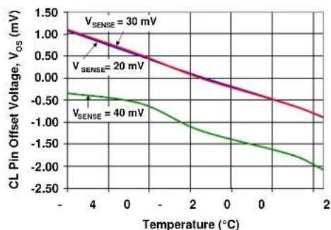
| Temperature (°C) | CL Pin Offset Voltage, Vos (mV) for V_SENSE = 30 mV | CL Pin Offset Voltage, Vos (mV) for V_SENSE = 20 mV | CL Pin Offset Voltage, Vos (mV) for V_SENSE = 40 mV | | ---------------- | -------------------------------------------------- | --------------------------------------------------- | --------------------------------------------------- | | -4 | 1.0 | 1.0 | -0.5 | | 0 | 0.5 | 0.5 | -1.0 | | 2 | 0.0 | 0.0 | -1.5 | | 4 | -0.5 | -0.5 | -2.0 | | 6 | -1.0 | -1.0 | -2.5 | | 8 | -1.5 | -1.5 | -2.5 | | 10 | -2.0 | -2.0 | -2.5 | | 12 | -2.5 | -2.5 | -2.5 | | 14 | -3.0 | -3.0 | -2.5 | | 16 | -3.5 | -3.5 | -2.5 | | 18 | -4.0 | -4.0 | -2.5 | | 20 | -4.5 | -4.5 | -2.5 |Data taken with the minimum following conditions:
$$ \begin{array}{l} I _ {P O S} = 5 \mathrm{mA} \ (E n a b l e s V _ {P O S} \text { at its self - regulating voltage) } \ V _ {R E F I N} = 2. 5 V, I _ {S E T} = 1 0 \mu A \ \end{array} $$
Note 1:
$$ \begin{array}{l} V _ {U V T H} > V _ {V R E F I N} \ V _ {O V T H} < V _ {V R E F I N} \ V _ {S E N S E} = 2 5 \mathrm{mV} \ V _ {V F B} = V _ {V N E G} \ V _ {D R A I N T H} = V _ {V N E G} \ V _ {O V O} = V _ {V N E G} \ V _ {C L} = V _ {V R E F I N} \ V _ {E N A B L E} = 5 V (\text { open }) \ V _ {\text { R E S T A R T }} = V _ {\text { V N E G }} (\text { o p e n }) \ \end{array} $$
FIGURE 2-24: CL pin Input Offset Voltage vs. Temperature.
line
| Temperature (°C) | Vfb = 0V (mV) | Vfb = 0.25V (mV) | Vfb = 1VV/fb = 0.5V (mV) | | ---------------- | ------------- | ---------------- | ------------------------ | | - | 50 | 35 | 15 | | 4 | 50 | 35 | 15 | | 0 | 50 | 35 | 15 | | 2 | 50 | 35 | 15 | | 0 | 50 | 35 | 15 | | 2 | 50 | 35 | 15 |Data taken with the minimum following conditions:
$$ \begin{array}{l} I _ {P O S} = 5 \mathrm{mA} \ (\text {Enables V} _ {P O S} \text {at its self - regulating voltage}) \end{array} $$
$$ V _ {R E F I N} = 2. 5 V, I _ {S E T} = 1 0 \mu A $$
Use TIMER pin as indicator
Note 1:
$$ \begin{array}{l} V _ {U V T H} > V _ {V R E F I N} \ V _ {O V T H} < V _ {V R E F I N} \ \begin{array}{r l} \mathrm {V _ {VFB}} & = \mathrm {V _ {NEG}}, \mathrm {V _ {NEG}} + 2 5 0 \mathrm{mV}, \ & \mathrm {V _ {NEG}} + 5 0 0 \mathrm{mv}, \mathrm {V _ {NEG}} + 1 \mathrm{V} \end{array} \ V _ {D R A I N T H} = V _ {V N E G} \ V _ {O V O} = V _ {V N E G} \ V _ {C L} = V _ {V R E F I N} \ V _ {E N A B L E} = 5 V (\text { open }) \ V _ {\text { RESTART }} = V _ {\text { VNEG }} (\text { open }) \ \end{array} $$
FIGURE 2-25: SENSE Pin Input Threshold vs. Temperature.

line
| OVO Voltage (V) | OV_TH Input High Voltage (V) | | --------------- | ---------------------------- | | 0 | 2.5 | | 1 | 4.0 | | 2 | 6.0 | | 3 | 6.5 | | 4 | 6.5 |Data taken with the minimum following conditions:
$$ I _ {P O S} = 5 \mathrm{mA} $$
(Enables V_POS at its self-regulating voltage)
$$ O V O = V _ {N E G} \text { to } 8 V $$
V_REFIN = 2.5V, I_SET = 10 A
Use PWRGOOD pin as indicator
Note 1:
$$ V _ {U V T H} > V _ {V R E F I N} $$
$$ V _ {S E N S E} = V _ {V N E G} $$
$$ V _ {V F B} = V _ {V N E G} $$
$$ V _ {D R A I N T H} = V _ {V N E G} $$
$$ V _ {C L} = V _ {V R E F I N} $$
$$ V _ {E N A B L E} = 5 V (\text { open }) $$
$$ V _ {\text { RESTART }} = V _ {\text { VNEG }} (\text { open }) $$
FIGURE 2-26: OV TH Input Rising Threshold vs. OVO Voltage.
line
| OVO Voltage (V) | T_A = +40°C | T_A = +25°C | T_A = +70°C | T_A = +85°C | T_A = 0°C | | --------------- | ----------- | ----------- | ----------- | ----------- | --------- | | 0 | 2.475 | 2.476 | 2.477 | 2.478 | 2.476 | | 1 | 2.475 | 2.476 | 2.477 | 2.478 | 2.476 | | 2 | 2.475 | 2.476 | 2.477 | 2.478 | 2.476 | | 3 | 2.475 | 2.476 | 2.477 | 2.478 | 2.476 | | 4 | 2.475 | 2.476 | 2.478 | 2.479 | 2.476 | | 5 | 2.475 | 2.476 | 2.478 | 2.479 | 2.476 | | 6 | 2.475 | 2.476 | 2.478 | 2.479 | 2.476 | | 7 | 2.475 | 2.476 | 2.478 | 2.479 | 2.476 | | 8 | 2.475 | 2.476 | 2.478 | 2.479 | 2.476 |Data taken with the minimum following conditions:
$$ I _ {P O S} = 5 \mathrm{mA} $$
(Enables V POS at its self-regulating voltage)
$$ O V O = V _ {N E G} \text { to } 8 \mathrm{V} $$
V_REFIN = 2.5V, I_SET = 10 A
Use PWRGOOD pin as indicator
Note 1:
$$ V _ {U V T H} > V _ {V R E F I N} $$
$$ V _ {S E N S E} = V _ {V N E G} $$
$$ V _ {V F B} = V _ {V N E G} $$
$$ V _ {D R A I N T H} = V _ {V N E G} $$
$$ V _ {C L} = V _ {V R E F I N} $$
$$ V _ {E N A B L E} = 5 V (\text { open }) $$
$$ V _ {\text { RESTART }} = V _ {\text { VNEG }} (\text { open }) $$
FIGURE 2-27: OV TH Input Falling
Threshold vs. OVO Voltage.
line
| Supply Current, I_POS (mA) | T_A = -40°C | T_A = 0°C | T_A = +25°C | T_A = +70°C | T_A = +85°C | | -------------------------- | ----------- | --------- | ----------- | ----------- | ----------- | | 5 | -9.95 | -10.00 | -10.05 | -10.10 | -10.15 | | 2 | -9.95 | -10.00 | -10.05 | -10.10 | -10.15 |Data taken with the minimum following conditions:
$$ I _ {P O S} = 5 \mathrm{mA} $$
(Enables V POS at its self-regulating voltage)
$$ V _ {R E F I N} = 2. 5 V, I _ {S E T} = 1 0 \mu A $$
Note 1:
$$ V _ {U V T H} < V _ {V R E F I N} $$
$$ V _ {O V T H} < V _ {V R E F I N} $$
$$ V _ {S E N S E} = V _ {V N E G} $$
$$ V _ {V F B} = V _ {V N E G} $$
$$ V _ {D R A I N T H} = V _ {V N E G} $$
$$ V _ {O V O} = V _ {V N E G} $$
$$ V _ {C L} = V _ {V R E F I N} $$
$$ V _ {E N A B L E} = 5 V (\text { open }) $$
$$ V _ {\text { R E S T A R T }} = V _ {\text { V N E G }} (\text { o p e n }) $$
FIGURE 2-28: UV Current vs. Supply Current (IPOS).

line
| Temperature (°C) | UV_HYS Pin Impedance (Ohms) | | ---------------- | --------------------------- | | - | 5000 | | 2 | 10000 | | 2 | 40000 |Data taken with the minimum following conditions:
$$ I _ {P O S} = 5 \mathrm{mA} $$
(Enables V_POS at its self-regulating voltage)
$$ \mathrm{UV} _ {\mathrm{TH}} < \mathrm{V} _ {\text { R E F I N }}, \quad \mathrm{UV} _ {\mathrm{TH}} > \mathrm{V} _ {\text { R E F I N }} $$
$$ V _ {R E F I N} = 2. 5 \mathrm{V}, I _ {S E T} = 1 0 \mu \mathrm{A} $$
Note 1:
$$ V _ {O V T H} < V _ {V R E F I N} $$
$$ V _ {S E N S E} = V _ {V N E G} $$
$$ V _ {V F B} = V _ {V N E G} $$
$$ V _ {D R A I N T H} = V _ {V N E G} $$
$$ V _ {O V O} = V _ {V N E G} $$
$$ V _ {C L} = V _ {V R E F I N} $$
$$ V _ {E N A B L E} = 5 V (\text { open }) $$
$$ V _ {\text { R E S T A R T }} = V _ {\text { V N E G }} (\text { o p e n }) $$
FIGURE 2-29: UV HYS Pin Impedance vs. Temperature.
line
| Temperature (°C) | UV_TH Rising Threshold (V) | | ---------------- | -------------------------- | | - | 2.5034 | | 2 | 2.5020 |Data taken with the minimum following conditions:
$$ I _ {P O S} = 5 \mathrm{mA} $$
(Enables V_POS at its self-regulating voltage)
$$ V _ {R E F I N} = 2. 5 \mathrm{V}, I _ {S E T} = 1 0 \mu \mathrm{A} $$
Use PWRGOOD pin as indicator
Note 1:
$$ V _ {O V T H} < V _ {V R E F I N} $$
$$ V _ {S E N S E} = V _ {V N E G} $$
$$ V _ {V F B} = V _ {V N E G} $$
$$ V _ {D R A I N T H} = V _ {V N E G} $$
$$ V _ {O V O} = V _ {V N E G} $$
$$ V _ {C L} = V _ {V R E F I N} $$
$$ V _ {E N A B L E} = 5 V (\text { open }) $$
$$ V _ {\text { RESTART }} = V _ {\text { VNEG }} (\text { open }) $$
FIGURE 2-30: UV TH Input Rising
Threshold vs. Temperature.

line
| Temperature (°C) | UV_TH Falling Threshold (V) | | ---------------- | --------------------------- | | -4 | 2.5027 | | 0 | 2.5025 | | 2 | 2.5020 | | 2 | 2.5015 |Data taken with the minimum following conditions:
$$ I _ {P O S} = 5 \mathrm{mA} $$
(Enables V_POS at its self-regulating voltage)
$$ V _ {R E F I N} = 2. 5 \mathrm{V}, I _ {S E T} = 1 0 \mu \mathrm{A} $$
Use PWRGOOD pin as indicator
Note 1:
$$ V _ {O V T H} < V _ {V R E F I N} $$
$$ V _ {S E N S E} = V _ {V N E G} $$
$$ V _ {V F B} = V _ {V N E G} $$
$$ V _ {D R A I N T H} = V _ {V N E G} $$
$$ V _ {O V O} = V _ {V N E G} $$
$$ V _ {C L} = V _ {V R E F I N} $$
$$ V _ {E N A B L E} = 5 V (\text { open }) $$
$$ V _ {\text { R E S T A R T }} = V _ {\text { V N E G }} (\text { o p e n }) $$
FIGURE 2-31: UV TH Input Falling
Threshold vs. Temperature.
line
| Temperature (°C) | OV_TH Rising Threshold (V) | | ---------------- | -------------------------- | | -4 | 2.5062 | | 2 | 2.5067 | | 2 | 2.5072 | | 2 | 2.5087 |Data taken with the minimum following conditions:
$$ \begin{array}{l} I _ {P O S} = 5 \mathrm{mA} \ (\text {Enables V_{POS} at its self - regulating voltage}) \end{array} $$
V_REFIN = 2.5V, I_SET = 10 A
Use PWRGOOD pin as indicator
Note 1:
$$ \begin{array}{l} V _ {O V T H} < V _ {V R E F I N} \ V _ {S E N S E} = V _ {V N E G} \ V _ {V F B} = V _ {V N E G} \ V _ {D R A I N T H} = V _ {V N E G} \ V _ {O V O} = V _ {V N E G} \ V _ {C L} = V _ {V R E F I N} \ V _ {E N A B L E} = 5 V (\text { open }) \ V _ {\text { R E S T A R T }} = V _ {\text { V N E G }} (\text { o p e n }) \ \end{array} $$
FIGURE 2-32: OV TH Input Rising Threshold vs. Temperature.

line
| Temperature (°C) | OV_TH Falling Threshold (V) | | ---------------- | --------------------------- | | -4 | 2.4780 | | 0 | 2.4790 | | 2 | 2.4795 | | 2 | 2.4800 |Data taken with the minimum following conditions:
$$ \begin{array}{l} I _ {P O S} = 5 \mathrm{mA} \ (\text {Enables V} _ {P O S} \text {at its self - regulating voltage}) \end{array} $$
V_REFIN = 2.5V, I_SET = 10 A
V_UVHYS = V_NEG
Use PWRGOOD pin as indicator
Note 1:
$$ \begin{array}{l} V _ {O V T H} < V _ {V R E F I N} \ V _ {S E N S E} = V _ {V N E G} \ V _ {V F B} = V _ {V N E G} \ V _ {D R A I N T H} = V _ {V N E G} \ V _ {O V O} = V _ {V N E G} \ V _ {C L} = V _ {V R E F I N} \ V _ {E N A B L E} = 5 V (\text { open }) \ V _ {\text { R E S T A R T }} = V _ {\text { V N E G }} (\text { o p e n }) \ \end{array} $$
FIGURE 2-33: OV_TH Input Falling Threshold vs. Temperature.
NOTES:
3.0 PIN DESCRIPTIONS
TABLE 3-1: MCP18480 PIN DESCRIPTIONS
| Pin Name | Pin Number | Pin Direction | Buffer Type | Description |
| SSOP | ||||
| V_POS | 1 I P | Positive supply input. | Internal Shunt Regulator connected between V_POS and V_NEG limits the potential to 12V between these two pins. A series resistor must be placed on the V_POS pin to limit the current into the device. | |
| OV_TH | 2 I A | Overvoltage | protection threshold. | An external resistor divider network is connected to this input pin to program the overvoltage protection threshold. The selected external resistor values for the OV_TH to system ground and OV_TH to V_NEG resistors should have currents in the 1 mA range. A typical Overvoltage threshold is -76V. Internal hysteresis in the overvoltage input comparator will allow proper operation once V_NEG falls below the selected threshold. |
| UV_TH | 3 I A | Undervoltage lockout | threshold.An external resistor divider network is connected to this input pin to program the undervoltage lockout threshold. If the voltage on UV_TH is less than V_NEG + 2.5V , the undervoltage comparator will trip, indicating an Undervoltage condition.An external hysteresis resistor can be used to set the high-to-low ( V_THF ) threshold below the low-to-high ( V_THR ) threshold. For telecom network equipment, it is desirable to have shutdown occur at -38.5V and the startup set at -43.0V. | |
| UV_HYS | 4 I A | Undervoltage | internal comparator hysteresis. | An external resistor is connected between this input to the UV_TH input pin to adjust the hysteresis of the internal Undervoltage comparator. Since it is desirable to shut down at -38.5V and restart at -43.0V in telecom switch equipment. |
| UV_D | 5 I/O | A Undervoltage event | delay.An external capacitor is connected to this input pin to set the delay between when the UV_TH pin drops below the trip point specified by the voltage on the V_REFIN pin and when the system shutdown occurs (causing the PWRGOOD pin to be driven to an inactive level and the GATE pin to be pulled to the V_NEG pin voltage level). The UV_D pin sources a current equivalent to the I_SET (in typical applications, the I_SET current equals 10 μA), which charges this external capacitor while an internal comparator compares this voltage on the UV_D pin to |V_REFIN|/2 .Typically, for telecom equipment, the system is expected to shut down when the input voltage falls below -38.5V (±1.0V DC) for greater than 100 ms. | |
Legend: TTL = TTL compatible input ST = Schmitt Trigger input with CMOS levels
I = Input
O = Output
P = Power
CMOS = CMOS-compatible input
A = Analog
D = Digital
TABLE 3-1: MCP18480 PIN DESCRIPTIONS (CONTINUED)
| Pin Name | Pin Number | Pin Direction | Buffer Type | Description |
| SSOP | ||||
| V_REFOUT | 6 O A | Reference output. | Internal reference output voltage (typically 2.5V). Usually tied back to the V_REFIN pin unless an external high-precision reference voltage is desired. | |
| V_REFIN | 7 I A | Reference input. | This pin allows a high-precision reference voltage for the following functions:Undervoltage ComparatorOvervoltage ComparatorDRAIN ComparatorCurrent Limit TimerIf the precision of the V_REFOUT output voltage is acceptable, tie the V_REFOUT pin to the V_REFIN pin. | |
| CL 8 I A Current Limit. | Input used to set the maximum current limit threshold allowed by the system via a resistor divider network (with the resistor R_CL1 between the V_REFIN pin and the CL pin and resistor R_CL between the V_NEG pin and the CL pin). If the voltage across the sense resistor exceeds the voltage on the CL pin, it implies that there is excessive current over the allowed limit and forces the GATE pin to the V_NEG pin voltage level without delay. | |||
| I_SET | 9 I A | Current source set. | Establishes the internal I_SOURCE for the following:Undervoltage DelayCurrent Limit TimerGATE Pin Source CurrentAn external resistor R_ISET from the I_SET pin must be connected to either the V_NEG pin or the V_REFIN pin to set I_BIAS , which will then establish the current sources throughout the device. The I_BIAS current is the same for either connection.Connecting the R_ISET resistor to the V_NEG pin will establish the PWRGOOD pin output polarity to be active-high. Connecting the R_SET resistor to the V_REFIN pin will establish the PWRGOOD pin output polarity to be active-low. | |
Legend: TTL = TTL compatible input ST = Schmitt Trigger input with CMOS levels
I = Input
O = Output
P = Power
CMOS = CMOS-compatible input
A = Analog
D = Digital
TABLE 3-1: MCP18480 PIN DESCRIPTIONS (CONTINUED)
| Pin Name | Pin Number | Pin Direction | Buffer Type | Description |
| SSOP | ||||
| TIMER 10 I A | Current Limit Timer. | The value of the external capacitor ( C_TIMER ) connected to the TIMER pin sets the two time periods used during a current-limit event. These are:• The time that the GATE pin will limit the current through the external FET• The time that the GATE pin will disable the external FETDuring current limit, a pull-up current source charges up the external capacitor. Until the voltage on the TIMER pin reaches V_REFIN/2 , the GATE pin is driven to maintain a reduced current flow determined by the V_DS of the external FET.While the capacitor is being discharged by the pull-down current (pull-up current is off), the GATE pin is at V_NEG and the PWRGOOD pin is deasserted. When the TIMER voltage falls below approximately 100 mV, the GATE pin turns on, if the pin is low, to reset the internal fault latch. If the pin is high, the GATE pin remains off until the ENABLE pin is forced low. It is then forced high or the pin is forced low (asserted).The PWRGOOD pin reasserts after the voltages on the DRAIN _TH and GATE pins meet the appropriate conditions.The TIMER pin pull-up current is proportioned to the I_ISET current (approximately a multiple of 16). | ||
| V_NEG | 11 I P | Negative supply input. | The negative voltage applied to the board by the backplane (typically the most negative voltage in the system). | |
| R_DISCH | 12 I A | External MOSFET activation delay.An external resistor ( R_RDISCH ) is connected between the R_DISCH pin and the V_NEG pin and is used to set the delay between the deactivation and activation of the external pass MOSFET during a current-limit event. The delay is set by the values of the external capacitor ( C_TIMER ) and the external resistor ( R_RDISCH ). The formulas are: T_DEACT = (C_TIMER × R_ISET) / 16 T_ACT = (9.2 × R_RDISCH × C_TIMER) | ||
Legend: TTL = TTL compatible input ST = Schmitt Trigger input with CMOS levels
I = Input
O = Output
P = Power
CMOS = CMOS-compatible input
A = Analog
D = Digital
TABLE 3-1: MCP18480 PIN DESCRIPTIONS (CONTINUED)
| Pin Name | Pin Number | Pin Direction | Buffer Type | Description |
| SSOP | ||||
| SENSE 13 I A | Over-current sense. | The voltage on the SENSE input pin is used to detect over-current conditions in the load connected to the external MOSFET. This pin is directly connected to the source of the MOSFET, with an external resistor (RSENSE) (typically a low resistance) connected between the source of the MOSFET and VNEG | ||
| GATE 14 O A | MOSFET | gate driver. | The GATE output pin attaches to the gate of the external MOSFET. The voltage on the GATE pin is pulled to the voltage on the VNEG pin whenever the voltage on the UVTH pin is less than the voltage on the VREFIN pin, or the voltage on the OVTH pin is greater than the voltage on the VREFIN pin.The GATE pin is also pulled to the voltage on the VNEG pin when the ENABLE input pin is low.When current limit is reached, the voltage on the GATE pin is adjusted to maintain a constant voltage across the RSENSE resistor while the CTIMER capacitor starts to charge. When the voltage on CTIMER exceeds VREFIN/2, the GATE pin is pulled to VNEG to turn off the external MOSFET. A RC network can be added from the GATE pin to the drain of the external MOSFET, along with a capacitor from the GATE pin to the VNEG pin, to control the slew rate of the GATE pin.The GATE pin pull-up current is proportioned to the ISET current. | |
| VFB | 15 I A | External MOSFET drain monitor. | The VFB input pin monitors the voltage at the drain of the external power MOSFET switch with respect to the voltage on the VNEG pin for use by the internal foldback circuitry. An external resistor divider network (RFB1 and RFB2) is attached between the drain of this external MOSFET and the VNEG pin (RFB1 is connected between the drain of the external MOSFET and the VFB pin, while RFB2 is connected between the VFB pin and the VNEG pin). This prevents high-voltage breakdown of the VFB input. | |
| DRAINTH | 16 I A | MOSFET drain comparator threshold. | This pin is used during the power-up sequence of the inserted board, and after any fault condition that ‘turns off’ the GATE pin drive. The voltage on the pin indicates when the external FET is fully enhanced by comparing the pin voltage to an internal reference voltage (approximately 100 mV derived from the internal band gap reference).An external resistor divider network (RDRAIN1 and RDRAIN2) is attached between the drain of this external MOSFET and the VNEG pin (RDRAIN1 is connected between the drain of the external MOSFET and the DRAINTH pin while RDRAIN2 is connected between the DRAINTH pin and the VNEG pin). |
Legend: TTL = TTL compatible input ST = Schmitt Trigger input with CMOS levels
I = Input
O = Output
P = Power
CMOS = CMOS-compatible input
A = Analog
D = Digital
TABLE 3-1: MCP18480 PIN DESCRIPTIONS (CONTINUED)
| Pin Name | Pin Number | Pin Direction | Buffer Type | Description |
| SSOP | ||||
| OVO 17 I A Overvoltage | detect. | Typically for normal operation. This pin is tied to V_NEG .This feature allows the overvoltage detection input to monitor an over-voltage condition across the power module. The voltage is sensed at the drain of the external MOSFET. The voltage across the load is internally determined based upon:The voltage difference between system ground and the voltage on the V_NEG pinThe voltage difference between the drain of the external FET and the voltage on the V_NEG pinAn external resistor divider network ( R_OVO1 and R_OVO2 ) is attached between the drain of the external MOSFET and the V_NEG pin ( R_OVO1 is connected between the drain of the external MOSFET and the OVO pin, while R_OVO2 is connected between the OVO pin and the V_NEG pin).When the voltage across the external MOSFET (source-to-drain) equals system ground voltage (- V_NEG +), the maximum desired load voltage, the GATE pin is forced to the voltage on the V_NEG pin (disabling the external MOSFET).To detect Overvoltage on the board (instead of the load) directly, connect the OVO pin to the V_NEG pin. | ||
| PWRGOOD 18 O D Power Good indicator. | This state of the output is determined by four conditions. These are:UndervoltageOvervoltageCurrent LimitExternal FET is fully-enhanced (from DRAIN _TH pin on power-up)PWRGOOD is a CMOS logic voltage ( V_NEG or V_NEG +12V).PWRGOOD is active when the device has completed power-up and the system is neither in an Undervoltage or Overvoltage condition.Connecting the R_ISET pin to the V_NEG pin configures the PWRGOOD pin to be active high. Connecting the R_SET pin to the V_REF pin configures the PWRGOOD pin to be active low. | |||
| ENABLE 19 I TTL Enable Gate driver. | Used to enable the GATE pin and assert the PWRGOOD pin. The ENABLE pin is active-high and is internally pulled up to 5V. This pin is pulled low by the user to clear the current limit latch when a current-limit fault occurs with high, or to disable the GATE pin.H = Enable the GATE and PWRGOOD pins.L = Disables the GATE pin, deasserts the PWRGOOD pin and clears current limit latch.When the ENABLE pin is high, fault conditions will disable the GATE pin and deasserts the PWRGOOD pin. | |||
Legend: TTL = TTL compatible input
I = Input
P = Power
A = Analog
ST = Schmitt Trigger input with CMOS levels
O = Output
CMOS = CMOS-compatible input
D = Digital
TABLE 3-1: MCP18480 PIN DESCRIPTIONS (CONTINUED)
| Pin Name | Pin Number | Pin Direction | Buffer Type | Description |
| SSOP | ||||
| 20 | I TTL Auto | -restart enable. | Enables the auto-restart feature of the device after an over-current fault. L = The internal fault latch is reset and the device attempts to restart with a frequency determined by the values of the external components C_TIMER and R_DISCH. H = The auto-restart is disabled, allowing the GATE pin to remain at the V_NEG pin voltage after an over-current fault. Internally pulled down to the V_NEG pin voltage. |
Legend: TTL = TTL compatible input ST = Schmitt Trigger input with CMOS levels
I = Input O = Output
P = Power CMOS = CMOS-compatible input
A = Analog D = Digital
4.0 APPLICATIONS INFORMATION
The MCP18480 can be programmed to have the PWRGOOD signal be either active-high or active-low via the I_SET pin and the connection of the external R_ISET resistor (see Section 6.8.8, "Bias Block"). If the R_ISET resistor is connected between I_SET and V_NEG , the PWRGOOD output pin is an active-high signal. If the R_ISET resistor is connected between I_SET and V_REFIN , the PWRGOOD output pin is an active-low signal.
For systems using an active-low-enabled DC/DC converter module, the MCP18480 should be programmed for a high-active PWRGOOD output. Tying the R_ISET resistor to the V_NEG pin configures the PWRGOOD to be an active-high signal. The active-high PWRGOOD switches on the external NPN and the collector of the external NPN (labeled as GOODPWR) is pulled to V_NEG , enabling a low-active GOODPWR and resulting in enabling the DC/DC module.
For active-high DC/DC converter modules, the MCP18480 should be programmed for a low active PWRGOOD output. Connecting R_ISET to the V_REFIN pin will enable an active-low PWRGOOD output. Refer to Figure 4-1 and Figure 4-2 for schematics.
Figure 4-1 shows a typical telecom application circuit where the DC/DC module is active-high. Figure 4-2 shows a typical telecom application circuit where the DC/DC module is active-low. The polarity of the MCP18480's PWRGOOD pin (active-high or active-low) is dependant on the state of the I_SET pin.
text_image
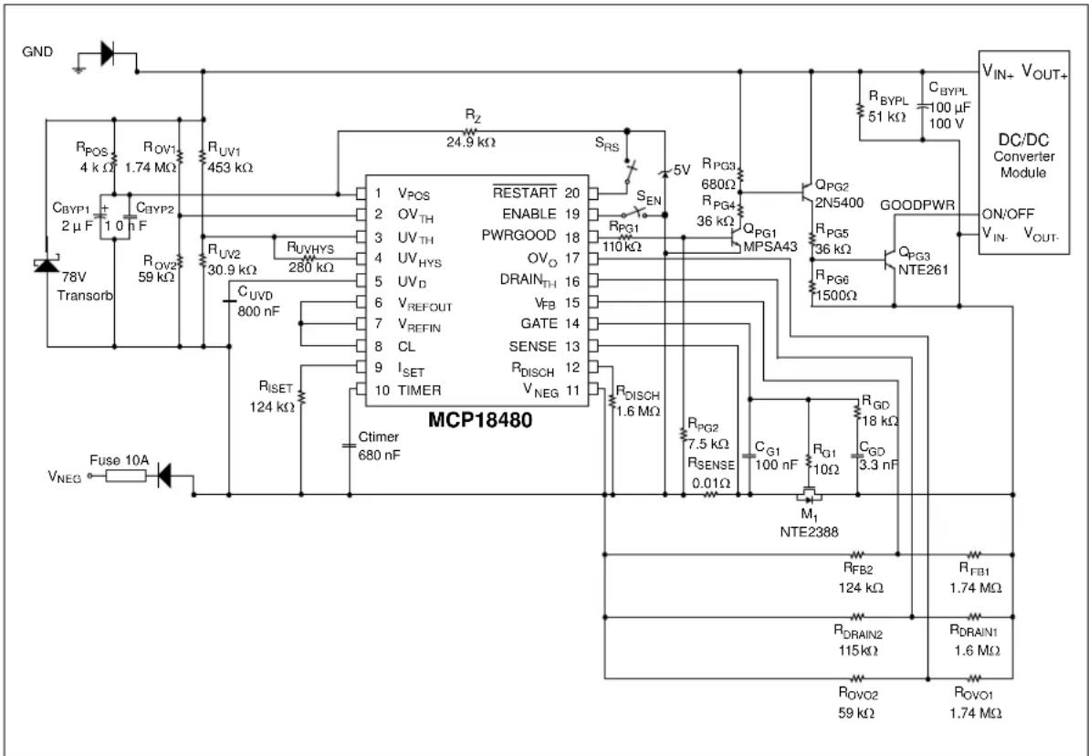
GND RPOS 4 kΩ CByP1 2 μF 78V Transorb ROV1 1.74 MΩ CByP2 1.0 nF RUV1 453 kΩ RUV2 59 kΩ CUVD 800 nF RUVHYS 280 kΩ RSET 124 kΩ Fuse 10A VNEG MCP18480 1 VPOS RESTART 20 2 OVTH ENABLE 19 3 UVTH PWRGOOD 18 4 UVHYS OVO 17 5 UVD DRAINTH 16 6 VREFOUT VFB 15 7 VREFIN GATE 14 8 CL SENSE 13 9 ISET RDISCH 12 10 TIMER VNEG 11 Ctimer 680 nF RPG1 110 kΩ SRS 5V RPG3 680Ω RPG4 36 kΩ QPG1 MPSA43 QPG2 2N5400 GOODPWR RPG5 36 kΩ RPG6 1500Ω QPG3 NTE261 RBPL 51 kΩ CByPL 100 μF 100 V ON/OFF VIN- VOUT- DC/DC Converter Module RFB2 124 kΩ RFB1 1.74 MΩ RSENSE 0.01Ω RPG2 7.5 kΩ RGD 18 kΩ CCL 100 nF RGS 10Ω CGS 3.3 nF M1 NTE2388 RDBAIN2 115kΩ RDRAIN1 1.6 MΩFIGURE 4-1: Typical Operating Circuit for Telecom Applications with Active-High power Module - foldback current limit enabled.
text_image
GND R_POS 4 kΩ C_BYP1 2 μF 78V Transorb R_OV1 1.74 MΩ C_BYP2 n F R_OV2 59 kΩ R_UV1 453 kΩ C_UVD 800 nF R_UV2 30.9 kΩ R_UVHYS 280 kΩ R_SET 124 kΩ V_NEG Fuse 10A MCP18480 Ctimer 680 nF 1 V_POS RESTART 20 2 OV_TH ENABLE 19 3 UV_TH PWRGOOD 18 4 UV_HYS OVO 17 5 UVD DRAIN_TH 16 6 V_REFOUT V_FB 15 7 VREFIN GATE 14 8 CL SENSE 13 9 I_SET R_DISCH 12 10 TIMER V_NEG 11 R_PG1 110 kΩ S_EN R_PG3 680Ω R_PG4 36 kΩ Q_PG1 MPSA43 5V R_PG3 Q_PG2 2N5400 GOODPWR Q_PG3 NTE261 R_PG6 1500Ω R_PG5 36 kΩ R_PG6 C_GI 100 nF R_GD 18 kΩ C_GD 3.3 nF R_DRAIN2 115 kΩ R_FB2 124 kΩ R_FB1 1.74 MΩ R_DRAIN1 1.6 MΩ DC/DC Converter Module ON/OFF V_IN- V_OUT+ R_BYPL 51 kΩ C_BYPL 100 μF 100 VFIGURE 4-2: Typical operating circuit for telecom applications with Active-Low power Module - foldback current limit enabled.
The MCP18480 can typically be implemented in a backplane system in one of two methods. Figure 4-3 shows a system where the backplane integrates the MCP18480 for every slot. Figure 4-4 shows a system where the backplane does not integrate the MCP18480s and each card that will be inserted into any slot is required to integrate the MCP18480.

flowchart
graph TD
    A["Card #1"] --> B["Card #2"]
    B --> C["Card #n"]
    C --> D["MCP18480"]
    B --> E["MCP18480"]
    A --> F["MCP18480"]
FIGURE 4-3: Backplane System Block Diagram #1.
flowchart
graph TD
    A["Card # 1\nMCP18480"] --> B["Card # 2"]
    B --> C["Card # n\nMCP18480"]
    C --> D["..."]
FIGURE 4-4: Backplane System Block Diagram #2.
NOTES:
5.0 POWER-UP
5.1 V POS and v_NEG Connection
For proper system operation, it is required that the system ground and the V_NEG pin have a solid connection before voltages are applied to any logic on the board.
5.2 The Board Circuitry
After the MCP18480 has "good" voltages on the V_POS and V_NEG pins, the board may have voltages applied to any of the other signals (a "good" voltage on V_POS indicates a "good" voltage on the system ground). The MCP18480 will start to source a small current to the external MOSFET to begin powering the board. This will turn on the MOSFET starting to power the external circuitry (load) of the board. The current from the GATE pin (into the external MOSFET) increases as the V_DS of the MOSFET decreases. When the V_DS of the MOSFET is below the voltage determined by the two resistors on the DRAIN TH pin ( RDRAIN1 and R_DRAIN2 ), and the voltage on the GATE pin is greater than 8V, the PWRGOOD pin is active.
6.0 INTERNAL SIGNAL DESCRIPTIONS
The figure on page 2 illustrates a block diagram of the MCP18480. Between the functional blocks, there are some signals that have been named. These signals are briefly explained in Section 6.1 thru Section 6.7.
6.1 Undervoltage Active
A signal that indicates (when low) that System Ground - V_NEG is less then the minimum voltage.
6.2 Overvoltage Active
A signal that indicates (when low) that System Ground -V_NEG is greater than the maximum voltage.
6.3 LATCHOFF
A signal that controls the GATE pin due to a timeout of the current-limiting timer.
6.4 Current Limit TIMER
A signal that controls the reduction of source current on the GATE pin and starts the voltage ramp of the current limit timer.
6.5 Current Limit Feedback
A voltage that is proportional to the V_DS of the external MOSFET to set a trip point for current-limiting.
6.6 TIMEOUT
A signal that indicates the completion of the foldback time and is used to start the latchoff time.
6.7 Circuit Breaker
A signal that immediately causes the GATE pin output to be driven to V_NEG upon the detection of excessive current in the external FET.
6.8 DESCRIPTION OF INTERNAL BLOCKS
The internal blocks shown in the MCP18480 Block Diagram on page 2 are discussed in Section 6.8.1 through Section 6.8.8.
Note: Voltage levels discussed are with respect to external component values selected in Figure 4-1.
6.8.1 UV (UNDERVOLTAGE) BLOCK
The Undervoltage lockout circuit monitors the input voltage by comparing a centertap voltage on an external resistor divider to a 2.5V reference. The centertap voltage is fed into the UV _TH input pin.
If the voltage on the UV_TH pin is below the internal 2.5V reference, the absolute magnitude of the supply voltage is too low for proper system operation, resulting in the external MOSFET being turned off. If the voltage on the UV_TH pin is greater than V_NEG + 2.5V , the supply voltage is above the minimal operating voltage as set by the external resistor divider network.
In telecom network applications, it is common to shut down the DC/DC converter supply when the input voltage falls below -38.5V (tolerance of ±1.0V ) for greater than 100 ms. The system will not restart until the voltage exceeds -43.0V (tolerance of ±0.5V ). This voltage difference is produced by an open-drain NMOS output (the UV_HYS pin) that connects an external resistor in parallel with the lower of the two resistors in the external UV divider network until the supply ramps down to -43V. When the UV_TH pin exceeds V_NEG + 2.5V , the internal NMOS transistor is turned off, disconnecting the external resistor connected to the UV_HYS pin. The voltage at the UV_TH pin increases to 2.79V. The supply voltage would have to decrease to -38.5V in order to assert the internal “Undervoltage Active” signal.
An internal 10 A current source and an external capacitor connected to the UV_D pin adjusts the delay between the input fault and the notification of this fault to the system. This is usually 100 ms for -48V telecom-type equipment. For customized adjustments, the time delay can be expressed as Equation 6-1.
EQUATION 6-1: INPUT FAULT DELAY
$$ T _ {D E L A Y} = \frac {\left(\frac {V _ {R E F I N}}{2}\right) \bullet C _ {U V D}}{1 0 \mu A} $$
C_UV is the capacitor connected between the UV_D pin and the V_NEG pin. A value of 1 F would provide a delay of about 100 ms.
If the supply voltage dips below the programmed threshold, the input comparator trips the other way. The timing capacitor is released to ramp-up at the previously described rate and the Undervoltage block switches when the capacitor voltage reaches 1.25V. When the input comparator goes to a low level, the hysteresis FET is turned on and the trip point for reassertion of good V_NEG reverts to -43V.
While the Undervoltage Active signal is low (includes Undervoltage input filter), the GATE pin driver for the external MOSFET is disabled, the GATE pin is pulled to the voltage of the V_NEG pin with a 60 mA current sink and the PWRGOOD output pin is deasserted to indicate that the input voltage is out of range.
EQUATION 6-2: UNDERVOLTAGE HYSTERESIS
$$ R _ {U V H Y S} = R \frac {R _ {U V I}}{\left(\frac {V _ {U V D}}{V _ {R E F I N}}\right) \frac {R _ {U V I}}{R _ {U V 2}}} l - $$
EQUATION 6-3: UNDERVOLTAGE CONDITION
$$ V _ {R E F I N} \frac {\left| V _ {N E G} \right| \bullet R _ {U V 2}}{R _ {U V 1} + (R _ {U V 2})} > \tag {1} $$
6.8.2 OV (OVERVOLTAGE) BLOCK
The overvoltage block behaves similarly to the under-voltage block in that it monitors an input voltage by comparing a centertap voltage on an external voltage divider (on the OV_TH pin) to the V_REFIN pin voltage.
If the centertap voltage is below the reference, the input voltage is not excessive. If the centertap voltage is greater than the V_NEG + V_REFIN pin voltages, the supply voltage is higher than the programmed acceptable maximum voltage limit. An internal flag is then activated to inform the MCP18480 that the input voltage has exceeded the preset limit.
The "Overvoltage Active" signal deasserts when the input voltage drops back below the threshold determined by the external resistors ( R_OV1 and R_OV2 ).
EQUATION 6-4: OVERVOLTAGE VOLTAGE CONDITION
$$ V _ {R E F I N} \frac {\left| V _ {N E G} \right| \bullet R _ {O V 2}}{R _ {O V 1} + (R _ {O V 2})} < $$
6.8.3 FET-GOOD BLOCK
The FET-good block monitors the voltage between the drain of the external MOSFET and on the V_NEG pin at power-up. It delays assertion of PWRGOOD until the drain-to-source voltage of the external FET is acceptably low and the voltage at the GATE pin is about 8V. The comparator operation is similar to Undervoltage and Overvoltage blocks.
To prevent applying excessive voltages to the gates of the FETs in the Undervoltage circuit, a resistive voltage divider is employed between ground and the V_NEG pin. Similarly, the drain of the external MOSFET can be exposed to voltages at around V_NEG during normal operation and as high as ground (typically 48V above V_NEG ).
The FET good block also monitors the GATE pin. When the GATE pin becomes >V_NEG + 8V and the DRAIN _TH pin is within its programmed range, the output of the FET good block is active.
The internal FET good signal goes high and remains active until a fault condition (Undervoltage, Overvoltage or Current Limit) is detected. Any of these conditions hold the PWRGOOD signal deasserted until the fault condition is removed and the external FET gate and drain voltages are acceptable.
6.8.4 CURRENT LIMIT BLOCK
An excessive current flowing through the external FET is sensed as a voltage across an external resistor connected between the FET's source and V_NEG .
The drain voltage is sensed with a resistor divider network, as shown in Figure 4-1 and Figure 4-2. The voltage tap is applied to a circuit whose output is 50 mV above V_NEG when the drain of the external FET is at V_NEG . The output is 12 mV when the V_FB pin is ≥ V_NEG + 0.5V . This output voltage is the Current Limit Feedback (CLFB) signal to the gate driver block for use in the fold-back current-limiting.
The CLFB voltage serves as the reference for a comparator whose other input monitors the voltage across the current limit sense resistor in series with the source of the external FET. When the SENSE pin exceeds the voltage on CLFB, a comparator output goes high to start the timer (see Section 6.8.5). The V_DS dependent threshold for the current limit helps keep the FET within its safe operating area.
Another comparator in the current-limiting block watches the SENSE pin for potentially catastrophic over-current conditions, which require immediate termination of conduction in the pass MOSFET. The output of this comparator trips a comparator used in the TIMER block to skip the first part of the timeout cycle and go straight to the "off" period. In some cases, the user may want to program the system to shut off immediately if there is a short-circuit condition that exceeds a desired level. To use this feature, connect a divider between the V_REFIN pin and the V_NEG pin, with its centertap at the CL input pin. The circuit breaker current that would trigger this mode is given by Equation 6-5.
EQUATION 6-5: CIRCUIT BREAKER THRESHOLD
$$ I _ {C A T} = \frac {\left(\frac {V _ {R E F I N}}{R _ {C L 1} + R _ {C L 2}}\right) \bullet R _ {C L 2}}{R _ {S E N S E}} $$
If this function is not needed in a particular application, it can be disabled by connecting the CL pin to the V_REFIN pin. Equation 6-6 shows the current of the CL pin during current-limiting.
EQUATION 6-6: CL PIN CURRENT
$$ \begin{array}{l} I _ {C L} = \frac {V _ {S E N S E}}{R _ {S E N S E}} \ \begin{array}{c} V _ {F B} \ \text { >0.5V } \ 0 V \ V _ {S E N S E} \end{array} \ V _ {S E N S E} \quad 0. 7 6 0. (0 5 V - \frac {V _ {D S} \times R _ {F B 2}}{R _ {F B 1} + R _ {F B 2}}) \quad 0. 0 1 2 V + \times = \ f o r V _ {F B} > 0. 5 V, V _ {S E N S E} = 0. 0 1 2 V \ \end{array} $$
6.8.5 TIMER BLOCK
Since the external FET can survive brief over-current episodes, it is unnecessary to turn off the FET instantly when the current rises too high (see external FET data sheet). The timer circuit uses the output of the comparator in the current-limiting block to begin charging an external capacitor with 16 · I_RISET (typically 160 A ) when an over-current condition is detected. When the voltage on the capacitor ramps up to 1.25V, a comparator output goes high. This output goes to another block that tells the gate driver to turn the external FET off and deassert the PWRGOOD pin. The complementary output of the timer changes the state of a hysteresis circuit that drops the reference input of the comparator to V_NEG + 100 mV (± 10 mV) .
When the FET is off, the current through it drops to zero, so that the voltage across the current sense resistor also goes to zero and the current limit signal to the timer block goes away. The timer capacitor starts to discharge at a rate set by the external resistor, P_DISCH .
Equation 6-7 shows the equations used to calculate the current at the TIMER pin. This current is used for other calculations.
EQUATION 6-7: TIMER PIN CURRENT CALCULATIONS
$$ I _ {T I M E R} = 1 6 \bullet I _ {R I S E T} \quad \text { Typical } $$
$$ I _ {T I M E R} = 1 0 \bullet I _ {R I S E T} \quad \text { Minimum } $$
$$ I _ {T I M E R} = 2 0 \bullet I _ {R I S E T} \quad \text { Maximum } $$
Legend: I_RISET is the current through the external R_ISET resistor
The delay between the inception of the over-current condition and the deactivation of the FET is given by Equation 6-8.
EQUATION 6-8: OVER-CURRENT FAULT DELAY
$$ T _ {C L D 1} = \frac {C _ {T I M E R}}{I _ {T I M E R}} \bullet 1. 2 5 $$
The time required to reset the timer and reactivate the gate driver is given by Equation 6-9.
EQUATION 6-9: OVER-CURRENT REACTIVATION DELAY
$$ T _ {C L D 2} = 9. 2 \mathbf {\Phi} _ {T I M E R} \bullet R _ {D I S C H} $$
As described above, the timer circuit operates as a free-running, multi-vibrator, if RESTART is low.
6.8.6 LATCH BLOCK
A current limit latch circuit determines whether, following the timeout period resulting from an over-current condition, the external FET should be latched-off until reactivated by an external signal, or be allowed to restart automatically following the timer cycle.
If the RESTART input is low, the part will restart and the gate drive to the external MOSFET will be restored automatically. If the RESTART pin is high, a current limit event will turn the FET off after the programmed delay and maintain an off condition until the ENABLE pin or RESTART pin is pulled low momentarily.
The GATE drive block sources a current equal to the voltage at CLFB divided by 1 kΩ to the gate of the external MOSFET. So the current sourced from the GATE pin is determined by the V_DS of the external FET. This current, and the external capacitors around the FET, control the slew rate of the drain of the external FET, limiting the current that would otherwise have to be diverted from other boards on the backplane. In the event of a problem (Overvoltage, Undervoltage or current limit), the gate of the external FET is pulled down with 60 mA. During normal operation, the GATE pin ramps up to about 12V, sending the external FET deeply into the triode region. If the drain current becomes excessive while the drain-to-source voltage is high, the inverting input of the op amp is driven to the CLFB voltage by the current-limiting block, causing a reduction in the drive to the external FET to reduce the current through it. This foldback current-limit remains active until the voltage on C_TIMER reaches V_REFIN/2 , after which the GATE output pin is pulled to V_NEG for the duration of the timeout period, or until ENABLE is cycled low momentarily.
For applications in which it is undesirable to have the drain current track the V_DS of the external pass FET in current limit, the user can tie the V_FB pin to the V_REF or V_NEG pin. This will make the MCP18480 try to force the drain current to 12 mV/ R_SENSE or 50 mV/ R_SENSE , respectively, until the TIMER block times out. If fold-back current-limiting is not desired at all, set the divider associated with the CL pin to detect the desired current in order to shut off the GATE immediately.
A voltage on the GATE pin higher than about 8V is one condition for the PWRGOOD pin to be asserted. Any fault condition that causes the GATE pin voltage to be pulled to V_NEG deasserts the PWRGOOD pin. On startup, a NMOS transistor with a resistor pulling its gate up holds the GATE pin down until the MCP18480 is properly biased.
6.8.8 BIAS BLOCK
The internal voltage generation or bias block generates the biasing currents for all internal blocks. It also provides a 2.5V reference voltage that is brought out to the V_REFOUT pin. This output pin is usually fed back into the V_REFIN pin. However, an externally-generated 2.5V reference voltage may be directly connected to the V_REFIN pin, while leaving the V_REFOUT pin unconnected. A V_REFIN/2 voltage is generated within the bias block, which is used as reference in the other blocks.
A internal shunt regulator limits the internal circuitry to 12V. An external current-limiting resistor in series with V_POS absorbs the excess voltage. The resulting regulated 12V source is used in the gate drive block and PWRGOOD output circuit.
The 12V source is also stepped-down to generate a 5V regulated source. Most of the other circuitry and blocks operate with the internally-generated 5V.
EQUATION 6-10: EXTERNAL R CURRENT ISET
$$ I _ {R I S E T} \quad \frac {\left(\frac {V _ {R E F I N}}{2}\right)}{R _ {I S E T}} \pm = $$
Note: The direction of the current is dependent on where the external R_ISET resistor is connected (the I_SET pin to either the V_NEG pin or the V_REFIN pin).
The “power good” block monitors the state of the OV active, the UV active, the current limit circuitry, and output of the FET good block to generate the PWRGOOD output signal.
NOTES:
7.0 PACKAGING INFORMATION
7.1 Package Marking Information
20-Lead SSOP

text_image
XXXXXXXXXX XXXXXXXXXX YYWWNNNExample:
text_image
MCP18480 I/SS 0348058Legend: XX...X Customer specific information*
YY Year code (last 2 digits of calendar year)
WW Week code (week of January 1 is week '01')
NNN Alphanumeric traceability code
Note: In the event the full Microchip part number cannot be marked on one line, it will be carried over to the next line thus limiting the number of available characters for customer specific information.
* Standard marking consists of Microchip part number, year code, week code, and traceability code.
20-Lead Plastic Shrink Small Outline (SS) - 209 mil, 5.30 mm (SSOP)
Note: For the most current package drawings, please see the Microchip Packaging Specification located at http://www.microchip.com/packaging

text_image
E E1 p B n 2 1 D
natural_image
Line drawing of an integrated circuit chip with multiple pins (no text or symbols)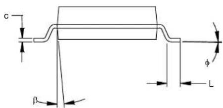
text_image
c β L φ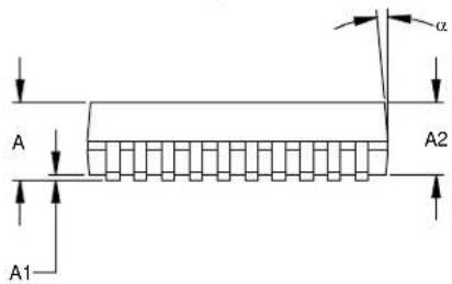
text_image
A A1 A2 α| Units | INCHES* | MILLIMETERS | |||||
| Dimension Limits | MIN | NOM | MAX | MIN | NOM | MAX | |
| Number of Pins | n | 20 | 20 | ||||
| Pitch | p | .026 | 0.65 | ||||
| Overall Height | A | .068 | .073 | .078 | 1.73 | 1.85 | 1.98 |
| Molded Package Thickness | A2 | 1.831.731.63.072.0 | |||||
| Standoff § | A1 | .002 | .006 | .010 | 0.05 | 0.15 | 0.25 |
| Overall Width | E | .299 | .309 | .322 | 7.59 | 7.85 | 8.18 |
| Molded Package Width | E1 | .201 | .207 | .212 | 5.11 | 5.25 | 5.38 |
| Overall Length | D | .278 | .284 | .289 | 7.06 | 7.20 | 7.34 |
| Foot Length | L | .022 | .030 | .037 | 0.56 | 0.75 | 0.94 |
| Lead Thickness | c | 0.250.180.10.010.0 | |||||
| Foot Angle | 203.201.01.600.0084( | ||||||
| Lead Width | B | .010 | .013 | .015 | 0.25 | 0.32 | 0.38 |
| Mold Draft Angle Top | 10501050 | ||||||
| Mold Draft Angle Bottom | 10501050 | ||||||
* Controlling Parameter
§ Significant Characteristic
Notes:
Dimensions D and E1 do not include mold flash or protrusions. Mold flash or protrusions shall not exceed
.010" (0.254mm) per side.
JEDEC Equivalent: MO-150
Drawing No. C04-072
APPENDIX A: REVISION HISTORY
Revision A
This is a new data sheet
Revision B
- Add device characterization information
• Enhanced functional description
Revision C
- Added note to the package outline drawing.
NOTES:
APPENDIX B: MCP18480 SCHEMATICS
This appendix contains the schematics for the MCP18480 Evaluation Board.
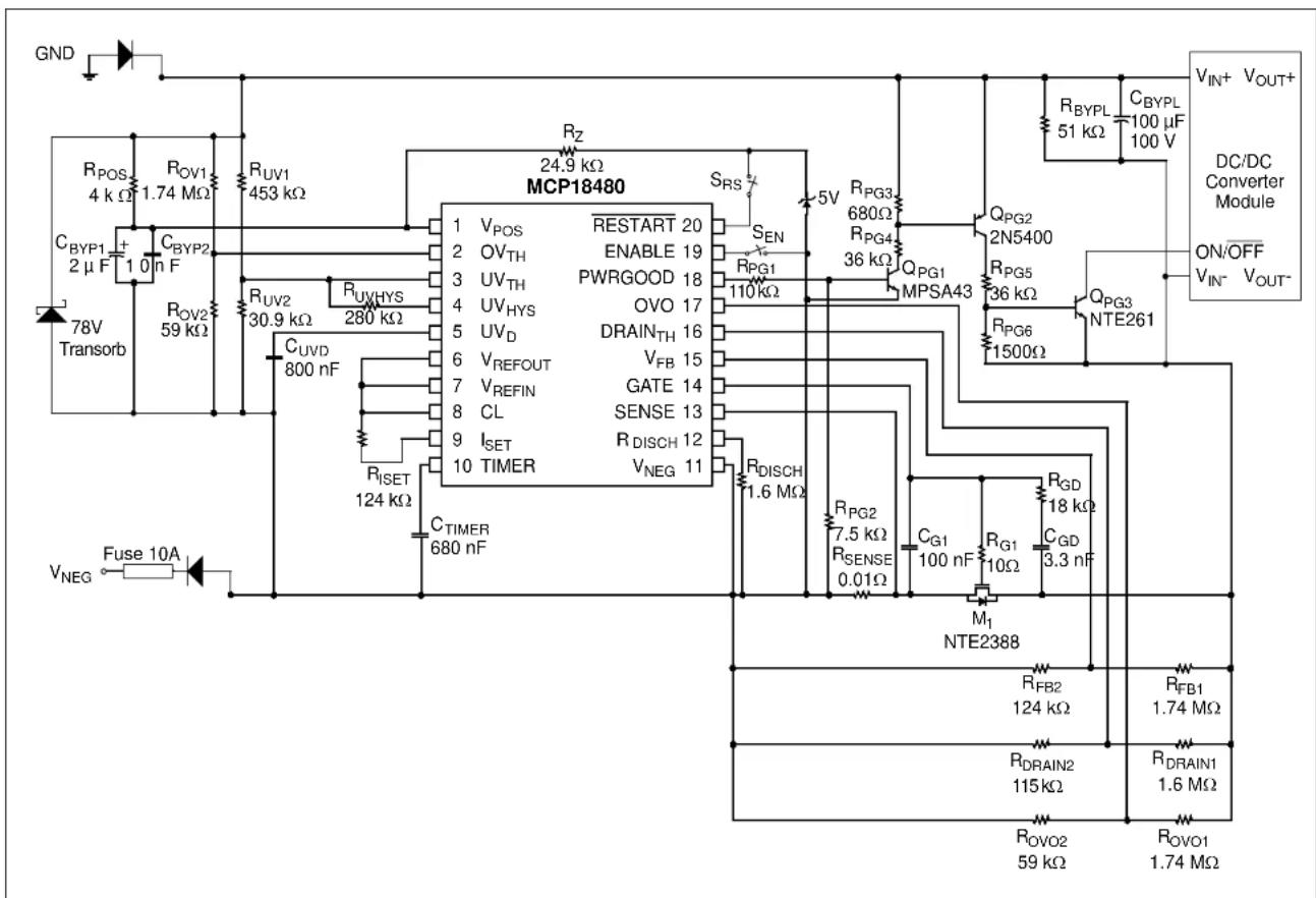
text_image
GND RPOS 4 kΩ C BYP1 2 μF 78V Transorb RUV1 1.74 MΩ C BYP2 n F RUV2 59 kΩ RUVHYS 30.9 kΩ CUVD 800 nF Riset 124 kΩ C_TIMER 680 nF MCP18480 1 V_POS RESTART 20 2 OV_TH ENABLE 19 3 UV_TH PWRGOOD 18 4 UV_HYS OVO 17 5 UV_D DRAIN_TH 16 6 V_REFOUT V_FB 15 7 V_REFIN GATE 14 8 CL SENSE 13 9 I_SET R_DISCH 12 10 TIMER V_NEG 11 SRS 5V RPG3 680Ω RPG4 36 kΩ QPG1 MPSA43 QPG2 2N5400 RPG5 36 kΩ QPG3 NTE261 RPG6 1500Ω C_GI 100 nF R_GD 18 kΩ C_GD 3.3 nF M1 NTE2388 R_FB2 124 kΩ R_FB1 1.74 MΩ R_DRAIN2 115 kΩ R_DRAIN1 1.6 MΩ R_OVO2 59 kΩ R_OVO1 1.74 MΩ V_IN+ V_OUT+ DC/DC Converter Module ON/OFF VIN- V_OUT- R_BYPL 51 kΩ C_BYPL 100 μF 100 VFIGURE B-1: Typical Operating Circuit for Telcom Applications with Active-High Power Module - Foldback Current Limit Enabled.

text_image
GND R_POS 4 kΩ C_BYP1 2 μF 78V Transorb R_OV1 1.74 MΩ C_BYP2 1.0 F R_UV1 453 kΩ R_UV2 30.9 kΩ C_UVD 800 nF R_UVHYS 280 kΩ R_SET 124 kΩ Fuse 10A MCP18480 1 V_POS 2 OV_TH 3 UV_TH 4 UV_HYS 5 UVD 6 V_REFOUT 7 V_REFIN 8 CL 9 I_SET 10 TIMER C_TIMER 680 nF S_RS 24.9 kΩ R_Z 5V R_PG3 680Ω PWRGOOD 18 OVO 17 DRAIN_TH 16 V_FB 15 GATE 14 SENSE 13 R_DISCH 12 V_NEG 11 R_PG4 36 kΩ Q_PG1 MPSA43 Q_PG2 2N5400 Q_PG3 NTE261 R_PG6 1500Ω R_PG5 36 kΩ R_PG1 100 nF R_GD 18 kΩ C_GD 3.3 nF C_TIMER 680 nF R_PG2 7.5 kΩ R_SENSE 0.01Ω R_DISCH 1.6 MΩ M_1 NTE2388 R_FB2 124 kΩ R_DRAIN2 115 kΩ R_OVO2 59 kΩ R_OVO1 1.74 MΩ R_FB1 1.74 MΩ R_DRAIN1 1.6 MΩ R_BYPL 51 kΩ C_BYPL 100 μF 100 V V_IN+ V_OUT+ DC/DC Converter Module ON/OFF V_IN- V_OUT- V_NEGA 1FIGURE B-2: Typical Operating Circuit for Telcom Applications with Active-Low Power Module - Foldback Current Limit Enabled.
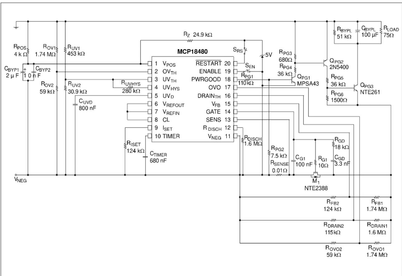
text_image
RPOS 4 kΩ C_BYP1 2 μF + - C_BYP2 10 nF R_UV1 453 kΩ R_UV2 59 kΩ C_UVD 800 nF R_UVHYS 30.9 kΩ R_UV2 30.9 kΩ MCP18480 1 V_POS 2 OV_TH 3 UV_TH 4 UV_HYS 5 UV_D 6 V_REFOUT 7 V_REFIN 8 CL 9 I_SET 10 TIMER C_TIMER 680 nF R_SET 124 kΩ S_RS R_Z 24.9 kΩ MCP18480 1 RESTART 20 2 ENABLE 19 3 PWRGOOD 18 4 OVO 17 5 DRAIN_TH 16 6 V_FB 15 7 GATE 14 8 SENS 13 9 R_DISCH 12 V_NEG 11 S_EN R_PG1 110 kΩ R_PG3 680 Ω R_PG4 36 kΩ Q_PG1 MPSA43 R_PG6 1500 Ω Q_PG2 2N5400 R_PG5 36 kΩ Q_PG3 NTE261 R_PG2 7.5 kΩ R_GD 18 kΩ C_G1 100 nF R_G1 10 Ω C_GD 3.3 nF M_1 NTE2388 R_FB2 124 kΩ R_FB1 1.74 MΩ R_DRAIN2 115 kΩ R_DRAIN1 1.6 MΩ R_OVO2 59 kΩ R_OVO1 1.74 MΩFIGURE B-3: Evaluation Board Schematic (Active-Low Power Module - Foldback Current Limit Enabled).
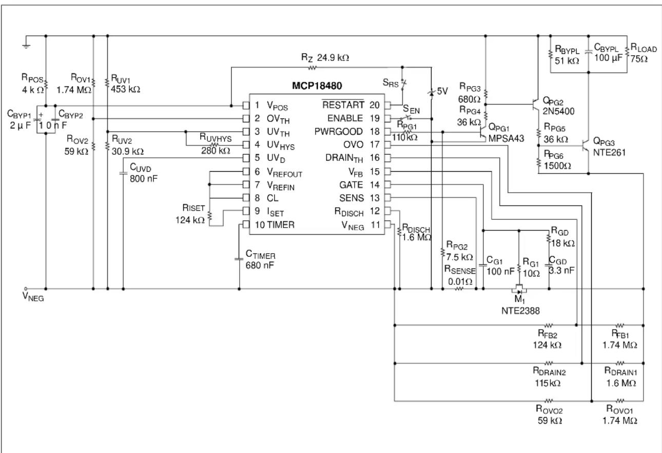
text_image
RPOS 4 kΩ CByP1 2 μF + - CByP2 1.0 nF RUV1 453 kΩ RUV2 59 kΩ CUVD 800 nF RUVHYS 280 kΩ RSET 124 kΩ CTIMER 680 nF MCP18480 1 VPOS 2 OVTH 3 UVTH 4 UVHYS 5 UVD 6 VREFOUT 7 VREFIN 8 CL 9 ISET 10 TIMER RISHT COUNTER 124 kΩ RESTART 20 ENABLE 19 PWRGOOD 18 OVO 17 DRAINTH 16 VFB 15 GATE 14 SENS 13 RDISH 12 VNEG 11 SRS 5V RPG3 680Ω RPG4 36 kΩ QPG1 MPSA43 QPG2 2N5400 RPG5 36 kΩ QPG3 NTE261 RPG6 1500Ω RPG2 7.5 kΩ RSENSE 0.01Ω RGD 18 kΩ CG1 100 nF RG1 10Ω CGD 3.3 nF M1 NTE2388 RFB2 124 kΩ RFB1 1.74 MΩ RDRAIN2 115 kΩ RDRAIN1 1.6 MΩ ROVO2 59 kΩ ROVO1 1.74 MΩFIGURE B-4: Evaluation Board Schematic (Active-High Power Module - Foldback Current Limit Enabled).

text_image
RPOS 4 kΩ CByP1 2 μF + - CByP2 1 0 nF RUV1 453 kΩ RUV2 59 kΩ CUVD 800 nF RCL1 (Note) 210 kΩ RCL2 (Note) 40.2 kΩ VNEG MCP18480 1 VPOS 2 OVTH 3 UVTH 4 UVHYS 5 UVD 6 VREFOUT 7 VREFIN 8 CL 9 ISET 10 TIMER RSET 124 kΩ CTIMER 680 nF RESTART 20 ENABLE 19 PWRGOOD 18 OVO 17 DRAINTH 16 VFB 15 GATE 14 SENS 13 RDISH 12 VNEG 11 SRS 5V RPG3 680Ω RPG4 36 kΩ QPG1 MPSA43 RPG2 7.5 kΩ RSENSE 0.01Ω RDISCH 1.6 MΩ RG1 10Ω CG1 100 nF MGD 18 kΩ CGD 3.3 nF M1 NTE2388 RDRAIN2 115 kΩ ROVO2 59 kΩ RDRAIN1 1.6 MΩ ROVO1 1.74 MΩ RBPL 51 kΩ CBPL 100 μF RLOAD 75ΩFIGURE B-5: Evaluation Board Schematic (Active-Low Power Module - Circuit Breaker Current Limit Enabled).
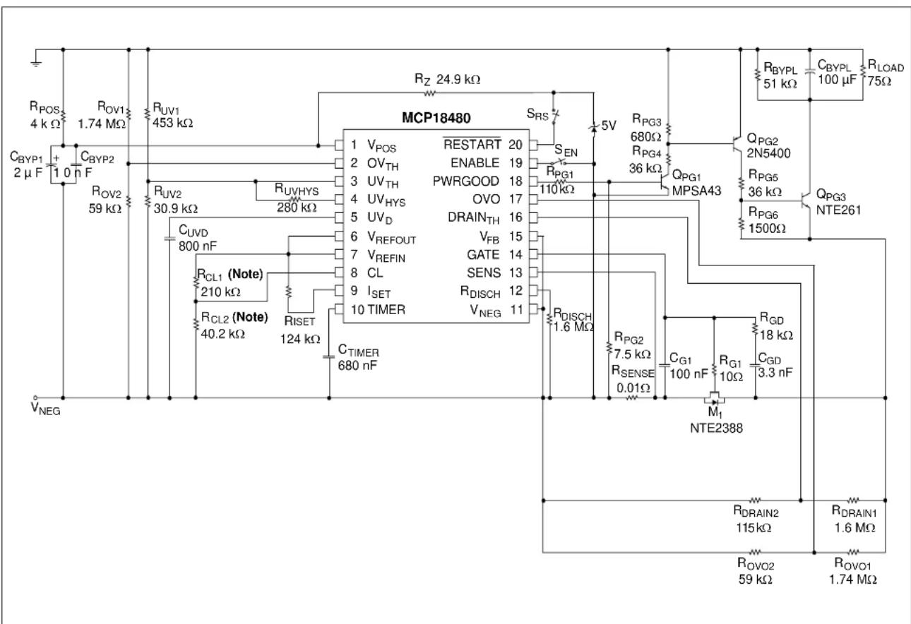
text_image
RPOS 4 kΩ CByP1 2 μF + - CByP2 1.0 nF RUV1 453 kΩ RUV2 59 kΩ CUVD 800 nF RCL1 (Note) 210 kΩ RCL2 (Note) 40.2 kΩ RISET 124 kΩ C_TIMER 680 nF MCP18480 1 V_POS RESTART 20 2 OV_TH ENABLE 19 3 UV_TH PWRGOOD 18 4 UV_HYS OVO 17 5 UV_D DRAIN_TH 16 6 V_REFOUT V_FB 15 7 V_REFIN GATE 14 8 CL SENS 13 9 I_SET R_DISCH 12 10 TIMER V_NEG 11 S_RS 5V RPG3 680Ω RPG4 36 kΩ QPG1 MPSA43 QPG2 2N5400 RPG5 36 kΩ RPG6 1500Ω QPG3 NTE261 RBYPL 51 kΩ CByPL 100 μF RLOAD 75Ω R_PG2 7.5 kΩ R_GD 18 kΩ C_G1 100 nF R_G1 10Ω C_GD 3.3 nF M1 NTE2388 R_DRAIN2 115 kΩ R_DRAIN1 59 kΩ ROVO2 ROVO1 1.6 MΩFIGURE B-6: Evaluation Board Schematic (Active-High Power Module - Circuit Breaker Current Limit Enabled).
NOTES:
PRODUCT IDENTIFICATION SYSTEM
To order or obtain information, e.g., on pricing or delivery, refer to the factory or the listed sales office.

text_image
PART NO. X /XX Device Range PackageTemperatureDevice MCP18480: -48V Hot Swap Controller
MCP18480T: -48V Hot Swap Controller
(Tape and Reel)
Temperature Range I = -40°C to +85°C
Package SS = Plastic SSOP (209 mil, Body), 20-lead
Examples:
a) MCP18480-I/SS = Industrial Temp., SSOP package
b) MCP18480T-I/SS = Tape and Reel, Industrial Temp., SSOP package
Sales and Support
Data Sheets
Products supported by a preliminary Data Sheet may have an errata sheet describing minor operational differences and recommended workarounds. To determine if an errata sheet exists for a particular device, please contact one of the following:
- Your local Microchip sales office
- The Microchip Corporate Literature Center U.S. FAX: (480) 792-7277
- The Microchip Worldwide Site (www.microchip.com)
Please specify which device, revision of silicon and Data Sheet (include Literature #) you are using.
Customer Notification System
Register on our web site (www.microchip.com/cn) to receive the most current information on our products.
NOTES:
Note the following details of the code protection feature on Microchip devices:
• Microchip products meet the specification contained in their particular Microchip Data Sheet.
- Microchip believes that its family of products is one of the most secure families of its kind on the market today, when used in the intended manner and under normal conditions.
- There are dishonest and possibly illegal methods used to breach the code protection feature. All of these methods, to our knowledge, require using the Microchip products in a manner outside the operating specifications contained in Microchip's Data Sheets. Most likely, the person doing so is engaged in theft of intellectual property.
- Microchip is willing to work with the customer who is concerned about the integrity of their code.
- Neither Microchip nor any other semiconductor manufacturer can guarantee the security of their code. Code protection does not mean that we are guaranteeing the product as "unbreakable."
Code protection is constantly evolving. We at Microchip are committed to continuously improving the code protection features of our products. Attempts to break Microchip's code protection feature may be a violation of the Digital Millennium Copyright Act. If such acts allow unauthorized access to your software or other copyrighted work, you may have a right to sue for relief under that Act.
Information contained in this publication regarding device applications and the like is provided only for your convenience and may be superseded by updates. It is your responsibility to ensure that your application meets with your specifications. MICROCHIP MAKES NO REPRESENTATIONS OR WARRANTIES OF ANY KIND WHETHER EXPRESS OR IMPLIED, WRITTEN OR ORAL, STATUTORY OR OTHERWISE, RELATED TO THE INFORMATION, INCLUDING BUT NOT LIMITED TO ITS CONDITION, QUALITY, PERFORMANCE, MERCHANTABILITY OR FITNESS FOR PURPOSE. Microchip disclaims all liability arising from this information and its use. Use of Microchip devices in life support and/or safety applications is entirely at the buyer's risk, and the buyer agrees to defend, indemnify and hold harmless Microchip from any and all damages, claims, suits, or expenses resulting from such use. No licenses are conveyed, implicitly or otherwise, under any Microchip intellectual property rights.
QUALITY MANAGEMENT SYSTEM CERTIFIED BY DNV = ISO/TS 16949=
Trademarks
The Microchip name and logo, the Microchip logo, dsPIC, FlashFlex, KEELOQ, KEELOQ logo, MPLAB, PIC, PICmicro, PICSTART, PIC ^32 logo, rfPIC, SST, SST Logo, SuperFlash and UNI/O are registered trademarks of Microchip Technology Incorporated in the U.S.A. and other countries.
FilterLab, Hampshire, HI-TECH C, Linear Active Thermistor, MTP, SEEVAL and The Embedded Control Solutions Company are registered trademarks of Microchip Technology Incorporated in the U.S.A.
Silicon Storage Technology is a registered trademark of Microchip Technology Inc. in other countries.
Analog-for-the-Digital Age, Application Maestro, BodyCom, chipKIT, chipKIT logo, CodeGuard, dsPICDEM, dsPICDEM.net, dsPICworks, dsSPEAK, ECAN, ECONOMONITOR, FanSense, HI-TIDE, In-Circuit Serial Programming, ICSP, Mindi, MiWi, MPASM, MPF, MPLAB Certified logo, MPLIB, MPLINK, mTouch, Omniscient Code Generation, PICC, PICC-18, PICDEM, PICDEM.net, PICkit, PICtail, REAL ICE, rfLAB, Select Mode, SQL, Serial Quad I/O, Total Endurance, TSHARC, UniWinDriver, WiperLock, ZENA and Z-Scale are trademarks of Microchip Technology Incorporated in the U.S.A. and other countries.
SQTP is a service mark of Microchip Technology Incorporated in the U.S.A.
GestIC and ULPP are registered trademarks of Microchip Technology Germany II GmbH & Co. & KG, a subsidiary of Microchip Technology Inc., in other countries.
All other trademarks mentioned herein are property of their respective companies.
© 2002-2012, Microchip Technology Incorporated, Printed in the U.S.A., All Rights Reserved.
Printed on recycled paper. ISBN: 9781620767283
Microchip received ISO/TS-16949:2009 certification for its worldwide headquarters, design and wafer fabrication facilities in Chandler and Tempe, Arizona; Gresham, Oregon and design centers in California and India. The Company's quality system processes and procedures are for its PIC® MCUs and dsPIC® DSCs, KEELoo® code hopping devices, Serial EEPROMs, microperipherals, nonvolatile memory and analog products. In addition, Microchip's quality system for the design and manufacture of development systems is ISO 9001:2000 certified.
Worldwide Sales and Service
AMERICAS
Corporate Office
2355 West Chandler Blvd.
Chandler, AZ 85224-6199
Tel: 480-792-7200
Fax: 480-792-7277
Technical Support:
http://www.microchip.com/
support
Web Address:
www.microchip.com
Atlanta
Duluth, GA
Tel: 678-957-9614
Fax: 678-957-1455
Boston
Westborough, MA
Tel: 774-760-0087
Fax: 774-760-0088
Chicago
Itasca,
Tel: 630-285-0071
Fax: 630-285-0075
Cleveland
Independence, OH
Tel: 216-447-0464
Fax: 216-447-0643
Dallas
Addison, TX
Tel: 972-818-7423
Fax: 972-818-2924
Detroit
Farmington Hills, MI
Tel: 248-538-2250
Fax: 248-538-2260
Indianapolis
Noblesville, IN
Tel: 317-773-8323
Fax: 317-773-5453
Los Angeles
Mission Viejo, CA
Tel: 949-462-9523
Fax: 949-462-9608
Santa Clara
Santa Clara, CA
Tel: 408-961-6444
Fax: 408-961-6445
Toronto
Mississauga, Ontario,
Canada
Tel: 905-673-0699
Fax: 905-673-6509
ASIA/PACIFIC
Asia Pacific Office
Suites 3707-14, 37th Floor
Tower 6, The Gateway
Harbour City, Kowloon
Hong Kong
Tel: 852-2401-1200
Fax: 852-2401-3431
Australia - Sydney
Tel: 61-2-9868-6733
Fax: 61-2-9868-6755
China - Beijing
Tel: 86-10-8569-7000
Fax: 86-10-8528-2104
China - Chengdu
Tel: 86-28-8665-5511
Fax: 86-28-8665-7889
China - Chongqing
Tel: 86-23-8980-9588
Fax: 86-23-8980-9500
China - Hangzhou
Tel: 86-571-2819-3187
Fax: 86-571-2819-3189
China - Hong Kong SAR
Tel: 852-2401-1200
Fax: 852-2401-3431
China - Nanjing
Tel: 86-25-8473-2460
Fax: 86-25-8473-2470
China - Qingdao
Tel: 86-532-8502-7355
Fax: 86-532-8502-7205
China - Shanghai
Tel: 86-21-5407-5533
Fax: 86-21-5407-5066
China - Shenyang
Tel: 86-24-2334-2829
Fax: 86-24-2334-2393
China - Shenzhen
Tel: 86-755-8203-2660
Fax: 86-755-8203-1760
China - Wuhan
Tel: 86-27-5980-5300
Fax: 86-27-5980-5118
China - Xian
Tel: 86-29-8833-7252
Fax: 86-29-8833-7256
China - Xiamen
Tel: 86-592-2388138
Fax: 86-592-2388130
China - Zhuhai
Tel: 86-756-3210040
Fax: 86-756-3210049
ASIA/PACIFIC
India - Bangalore
Tel: 91-80-3090-4444
Fax: 91-80-3090-4123
India - New Delhi
Tel: 91-11-4160-8631
Fax: 91-11-4160-8632
India - Pune
Tel: 91-20-2566-1512
Fax: 91-20-2566-1513
Japan - Osaka
Tel: 81-66-152-7160
Fax: 81-66-152-9310
Japan - Yokohama
Tel: 81-45-471-6166
Fax: 81-45-471-6122
Korea - Daegu
Tel: 82-53-744-4301
Fax: 82-53-744-4302
Korea - Seoul
Tel: 82-2-554-7200
Fax: 82-2-558-5932 or
82-2-558-5934
Malaysia - Kuala Lumpur
Tel: 60-3-6201-9857
Fax: 60-3-6201-9859
Malaysia - Penang
Tel: 60-4-227-8870
Fax: 60-4-227-4068
Philippines - Manila
Tel: 63-2-634-9065
Fax: 63-2-634-9069
Singapore
Tel: 65-6334-8870
Fax: 65-6334-8850
Taiwan - Hsin Ch
Tel: 886-3-5778-366
Fax: 886-3-5770-955
Taiwan - Kaohsiung
Tel: 886-7-213-7828
Fax: 886-7-330-9305
Taiwan - Taipei
Tel: 886-2-2508-8600
Fax: 886-2-2508-0102
Thailand - Bangkok
Tel: 66-2-694-1351
Fax: 66-2-694-1350
EUROPE
Austria - Wels
Tel: 43-7242-2244-39
Fax: 43-7242-2244-393
Denmark - Copenhagen
Tel: 45-4450-2828
Fax: 45-4485-2829
France - Paris
Tel: 33-1-69-53-63-20
Fax: 33-1-69-30-90-79
Germany - Munich
Tel: 49-89-627-144-0
Fax: 49-89-627-144-44
Italy - Milan
Tel: 39-0331-742611
Fax: 39-0331-466781
Netherlands - Drunen
Tel: 31-416-690399
Fax: 31-416-690340
Spain - Madrid
Tel: 34-91-708-08-90
Fax: 34-91-708-08-91
UK - Wokingham
Tel: 44-118-921-5869
Fax: 44-118-921-5820
10/26/12