MIC2111B - Electronic controller Microchip - Free user manual and instructions
Find the device manual for free MIC2111B Microchip in PDF.

User questions about MIC2111B Microchip
0 question about this device. Answer the ones you know or ask your own.
Ask a new question about this device
Download the instructions for your Electronic controller in PDF format for free! Find your manual MIC2111B - Microchip and take your electronic device back in hand. On this page are published all the documents necessary for the use of your device. MIC2111B by Microchip.
USER MANUAL MIC2111B Microchip
Micrel's MIC2111B is a programmable-frequency, valley-current/voltage-mode PWM controller that provides the control and protection features necessary for power devices and drivers that use current sensing across the inductor. The MIC2111B can provide single tri-state PWM logic signal to work with either power-stage modules or discrete driver and MOSFETs. The device has precision enable and power-good (PG) functions for sequencing of multiple power supplies. In addition, the solution is compatible with intelligent power stages in a high-current, step-down DC/DC converter.
To optimize system size and system efficiency, the MIC2111B frequency can be programmed from 200kHz to 2MHz. The device operates in power-saving mode at light loads by reducing frequency. Optional outside audio range operation is possible when the power-stage is configured in light load mode. The solution uses differential current sensing for better current-limit accuracy and a dedicated differential amplifier for remote output sensing for accurate output voltage control. The MIC2111B has a high-gain transconductance amplifier for loop compensation. External slope compensation can be added through a resistor to avoid sub-harmonic oscillations. Other features include programmable OCP, output OVP, and thermal OTP protections. The MIC2111B offers Micrel's proprietary bi-directional, single wire fault communication for total system protection.
The MIC2111B is available in a 20-pin 3mm × 3mm TQFN package and has a junction temperature range of -40°C to +125°C.
Datasheets and support documentation are available on Micrel's web site at: www.micrel.com.
Features
• Single 3.3V or 5V supply
• Supports load currents up to 40A
- Programmable valley-current/voltage-mode PWM architecture
- 3.3V logic PWM output compatible with power-stage modules and DrMOS modules
- Single tri-state PWM output
- Programmable switching frequency: 200kHz to 2MHz.
- Differential remote sensing for output voltage and inductor current
- 0.6V reference voltage with total ±1% accuracy for output
- Adjustable soft-start/soft-stop and pre-biased safe startup.
• Supports light load and outside audio modes
- Programmable slope compensation and loop compensation
- Enable input, power-good (PG) output for sequencing
- Programmable OCP, output OVP, thermal OTP, and dedicated FAULTb pin for system safe startup/stop
- Internal thermal shutdown and UVLO
- -40^ to +125^ junction temperature range
• Available in 20-pin 3mm × 3mm TQFN package
Applications
- Servers and work stations
- Routers, switches, networking/telecom infrastructure
- Printers, scanners, graphics and video cards
• High current, high-performance POLs
Typical Application
text_image
5V OR 3.3V R1 10kΩ C1 1μF VCC AGND PG EN COMP SS R2* FREQ R3 R4 SEL TJ SLOPE R6 150kΩ 12V_BUS HS LS R7* DrMOS THWN# FAULTb ISEN+ ISEN- RS+ RS- *OPTIONAL COMPONENT VOUT 82pF R5 10kΩ C3 1nF R8* 8kΩ R9 10kΩ R10* 10kΩ R11 10kΩMIC2111B and DrMOS for a 25A Synchronous Buck Converter
Ordering Information
| Part Number | Switching Frequency | Junction Temperature Range | Current-Sense Gain | Power Stage | Package | Lead Finish |
| MIC2111BYMT | 200kHz to 2MHz | -40°C to +125°C | 30V/V DrMOS | 20-Pin 3mm × 3mm TQFN | Pb-Free |
Pin Configuration

text_image
COMP FB VDIFF RS- RS+ 20 19 18 17 16 SLOPE 1 15 FAULTb EN 2 14 ISEN+ SEL 3 13 ISEN- OVP 4 12 AGND FREQ 5 11 VCC TJ PG SS LS HS20-Pin 3mm × 3mm TQFN (MT) (Top View)
Pin Description
| Pin Number | I/O | Pin Name | Pin Name |
| 1 | SLOPE | Valley Current Mode: Slope compensation can be adjusted by adding a resistor from this pin to VIN (input power supply).Voltage Mode: Artificial ramp controlled by SLOPE resistor | ||
| 2 | EN | Enable (Input): A logic signal to enable or disable the controller. The EN pin is CMOS compatible. Logic high = enable, logic low = disable or shutdown. Do not leave floating. | ||
| 3 | SEL | Control-Mode Selection Pin: Connect this pin to AGND for valley current-mode operation.Leave this pin open for voltage mode control operation. | ||
| 4 | OVP | Output OVP programming pin. Connect a resistive divider to set OVP.OVP pin has 0.6V reference (seeFunctional Descriptionfor more details). | ||
| 5 | FREQ | Switching Frequency Adjust (Input): Connect a resistor from this pin to GND to set the switching frequency. | ||
| 6 | TJ | Power Module Temperature Sense Pin. Connect resistor divider to program TJ. TJ comparator has 0.6V reference (seeFunctional Descriptionfor more details). | ||
| 7 | O | PG | Power Good (Output): Open drain output, an external resistor to V_OUT is required for pull-up. |
| 8 | SS | Soft-start pin for limiting inrush current. A resistor from this pin to ground sets the soft-start time. If enabled, soft-stop time is same as soft-start. Contact factory for soft stop. | ||
| 9 I/O LS | Low-Side Logic Output. Connect this pin to module-mode pin for outside audio operation.Leave this pin open if outside audio (>25kHz) operation is not required. Current limit can be adjusted by connecting a resistor from LS to AGND (see Table 1 for details). | ||
| 10 O HS | High-Side Logic of Power Module Top FET. Connect this pin to the PWM pin of power module.This pin has tri-state capability. | ||
| 11 | P | VCC | 5V Supply Input. A 1μF ceramic capacitor from VCC to AGND is required for decoupling. |
| 12 P AGND Analog Ground. | |||
| 13 I | ISEN- | Negative pin of the inductor current-sense input. | |
| 14 | I | ISEN+ | Positive pin of the inductor current-sense input. |
| 15 | I/O | FAULTb | Bi-Directional Pin. This pin goes low if controller or module is not ready. This pin goes low if V_CC is less than UVLO, or if a TJ or OVP fault is triggered. Either VCC cycling or EN cycling is required to clear the fault. This pin has an internal 100kΩ pull-up resistor to VCC |
| 16 | I | RS+ | The non-inverting input of the remote sensing amplifier. Remote sense for output voltage. |
| 17 | I | RS- | The inverting input of the remote sensing amplifier. Remote sense for GND. |
| 18 | O | VDIFF | Output of differential amplifier. Connect a resistor divider from VDIFF to set output voltage |
| 19 | I | FB | The inverting input of the error amplifier. |
| 20 | I/O | COMP | Transconductance Amplifier Output. Connect compensation network from COMP node for frequency response. |
Absolute Maximum Ratings ^(1)
V_CC to AGND -0.3V to +6.0V
V_EN/SS, V_FREQ to AGND....-0.3V to (V_CC + 0.3V)
V_OVP, V_TJ, V_FAULTb to AGND -0.3V to (V_CC + 0.3V)
V_RS±, V_HS/LS, V_ISEN±, V_FB to AGND ..... -0.3V to (V_CC + 0.3V)
V_SLOPE to AGND....-0.3V to 20V
Junction Temperature ....+150°C
Storage Temperature (T _s )......-65°C to +150°C
Lead Temperature (soldering, 10s)....260°C ESD
Human Body Model ^(3) 2kV
Machine Model 200V
Operating Ratings ^(2)
Supply Voltage (Vcc) 3.135V to 5.5V
Enable Input (V EN )...... 0V to V CC
Junction Temperature (T _J )......-40°C to +125°C
Junction Thermal Resistance
20-Pin 3mm × 3mm TQFN ( _JA ) .....60°C/W
20-Pin 3mm × 3mm TQFN ( _JC ) .....10°C/W
Electrical Characteristics ^(4)
V_CC=5V; T_A=25^ , unless noted. Bold values indicate -40^≤ T_J≤+125^ .
| Parameter | Condition | Min. | Typ. | Max. | Units |
| Power Supply Input (VCC) | |||||
| VCC Input Voltage Range | Valley current mode, voltage mode | 3.135 | 5.5 | V | |
| VCC UVLO Threshold | V_CC rising | 2.75 | 2.85 | 2.95 | V |
| VCC UVLO Hysteresis | 100 | mV | |||
| Quiescent Supply Current | No switching, V_FB >0.8V | 2.1 | mA | ||
| Shutdown Supply Current | V_EN = 0V | 10 | μA | ||
| Output Voltage | |||||
| Output Voltage | 0.6 | 3.46 | V | ||
| Minimum V_CC -to-Output Set Point | Minimum V_CC - V_OUT headroom required | 1.3 | V | ||
| Voltage Accuracy | (RS+) - (RS-) | 0.594 | 0.6 | 0.606 | V |
| Remote Sense Amplifier Gain | V_DIFF/[(V_RS+) - (V_RS-)], V_RS- = 0V; V_RS+ = 3.6V | 0.997 | 1.000 | 1.003 | V/V |
| Remote Sense Amplifier Source/Sink Current | 550 | μA | |||
| RS+ Input Impedance | 175 | kΩ | |||
| RS- Input Impedance | 87 | kΩ | |||
| RS+/RS- Common-Mode Voltage | 100 | mV | |||
| FB Bias Current | V_FB = 0.6V | 5 | 100 | nA | |
| Transconductance Error Amplifier | |||||
| Error Amplifier Transconductance | FB-to-COMP g_m | 2 | mS | ||
| Error Amplifier Source/Sink Current | 175 | 220 | μA | ||
Notes:
- Exceeding the absolute maximum rating may damage the device.
- The device is not guaranteed to function outside operating range
- Devices are ESD sensitive. Handling precautions recommended. Human body model is 1.5kΩ in series with 100pF.
- Specification for packaged product only.
Electrical Characteristics ^(4) (Continued)
V_CC=5V; T_A=25^ , unless noted. Bold values indicate -40^≤ T_J≤+125^ .
| Parameter | Condition | Min. | Typ. | Max. | Units |
| Enable/Soft-Start/Soft-Stop | |||||
| EN Threshold Voltage | EN rising, point at which the output is enabled | 1.0 | 1.2 | 1.3 | V |
| EN Hysteresis | 50 | mV | |||
| Soft-Start time R | ss = Floating | 2 | ms | ||
| Soft-Stop Time^(5) | R_SS = Floating | 2 | ms | ||
| Oscillator and PWM | |||||
| Switching Frequency | R_FREQ = 49.9k | 1.6 | 2 | 2.4 | MHz R |
| FREQ = 100k | 0.85 | 1 | 1.15 | ||
| R_FREQ = 499k | 0.16 | 0.2 | 0.24 | ||
| Minimum Duty Cycle V | FB = 0.8V | 0 | % | ||
| Minimum Off-Time CCM | 100 | ns | |||
| Minimum On-Time CCM | 40 | ns | |||
| HS, LS Logic High Voltage | I_LOAD = 50mA | 4 | V | ||
| HS, LS Logic Low Voltage | I_LOAD = 50mA | 0.8 | V | ||
| HS Tri-State Leakage Current | V_HS = 1.5V | -1 | 1 | μA | |
| LS Tri-State Leakage Current | V_LS = 1.5V | -1 | 1 | μA | |
| HS, LS Rise/Fall Time | Q_LOAD = 20pF | 1 | ns | ||
| Outside Audio DCM time | No Load | 32 | μs | ||
| Current-Sense Amplifier | |||||
| Current Amplifier Gain | 30 | V/V | |||
| Current Amplifier Bandwidth | 3dB bandwidth | 10 | MHz | ||
| Current-Limit Threshold | LS = 0.5V | 15 | 18.3 | 22.5 | mV |
| LS = 0.7V | 20 | 23.3 | 27.5 | ||
| ISEN+ISEN Input Bias Current | 0.01 | 0.1 | μA | ||
| Slope Compensation | |||||
| V_SLOPE Common-Mode Range | 0.6 | 3.46 | V | ||
| SLOPE Sink Current | Valley Current Mode | 280 | μA | ||
| Power Good (PG) | |||||
| Power Good Threshold Voltage | FB rising | 90 | 92 | 95 | %VOUT |
| Power Good Hysteresis | 2 | %VOUT | |||
| Power Good Delay | FB rising, delay from FB high to PG high | 200 | μs | ||
| Power Good Low Voltage | V_FB < 90% × V_NOM, I_PG = 1mA | 12 | 200 | mV | |
Note:
5. Soft-stop is disabled by default. Contact factory to enable soft-stop.
Electrical Characteristics ^(4) (Continued)
V_CC=5V; T_A=25^ , unless noted. Bold values indicate -40^≤ T_J≤+125^
| Parameter | Condition | Min. | Typ. | Max. | Units |
| FAULTb | |||||
| FAULTb Threshold Voltage | FAULTb rising | 2 | 3.1 V | ||
| FAULTb Hysteresis 1.1 V | |||||
| FAULTb Low Voltage I | _LOAD = 500μA | 10 | 50 | mV | |
| FAULTb Leakage Current | 1 | μA | |||
| OVP | |||||
| OVP Threshold Voltage | OVP rising | 0.585 | 0.6 | 0.615 | V |
| OVP Hysteresis | 20 | mV | |||
| Thermal Shutdown | |||||
| TJThreshold Voltage TJ | J rising | 0.585 | 0.6 | 0.615 | V |
| TJHysteresis | 50 | mV | |||
| Internal Thermal Shutdown | Temperature rising | 155 | °C | ||
| Internal Thermal Shutdown Hysteresis | 20 | °C | |||
Functional Block Diagram

flowchart
graph TD
    A["VCC 100K"] --> B["地"]
    B --> C["SEL VCC"]
    C --> D["UVLO"]
    D --> E["CONTROL SELECTION"]
    E --> F["CONTROL LOGIC"]
    F --> G["SLOPE"]
    F --> H["ISEN-"]
    F --> I["ISEN+"]
    F --> J["CURRENT LIMIT"]
    J --> K["HS"]
    J --> L["LS"]
    M["EN FAULTb"] --> N["VREF"]
    N --> O["THERMAL SHUTDOWN"]
    P["TJ"] --> Q["VREF"]
    Q --> R["AMP"]
    S["OVP"] --> T["AMP"]
    U["PG"] --> V["AMP"]
    W["VREF 92%"] --> X["VREF FB"]
    Y["Gm 0.6V"] --> Z["SOFT-START"]
    AA["VREF 0.6V"] --> AB["AMP"]
    AC["FREQ"] --> AD["OSC"]
    AE["RS+"] --> AF["AMP"]
    AG["RS-"] --> AH["AMP"]
    AI["VDIFF"] --> AJ["AMP"]
    AK["COMP"] --> AL["AMP"]
    AM["FB"] --> AN["AMP"]
    AO["SS"] --> AP["AMP"]
    AQ["AGND"] --> AR["AMP"]
Typical Characteristics
Refer to Typical Application Schematic.
Efficiency vs. Output Current (V_OUT = 1.2V)

line
| OUTPUT CURRENT (A) | EFFICIENCY (%) | | ------------------ | -------------- | | 0 | 0 | | 5 | 30 | | 10 | 70 | | 15 | 85 | | 20 | 90 | | 25 | 90 | | 30 | 85 | | 35 | 80 | | 40 | 75 | | 45 | 70 | | 50 | 65 | | 55 | 60 | | 60 | 55 | | 65 | 50 | | 70 | 45 | | 75 | 40 | | 80 | 35 | | 85 | 30 | | 90 | 25 | | 95 | 20 | | 100 | 15 |Efficiency vs. Output Current (V_IN = 12V)

line
| OUTPUT CURRENT (A) | EFFICIENCY (%) | | ------------------ | -------------- | | 0 | 0 | | 5 | ~85 | | 10 | ~90 | | 15 | ~90 | | 20 | ~88 | | 25 | ~87 |EN Threshold vs. V_cc Change
line
| V_cc (V) | ENABLE THRESHOLD (V) | | -------- | ------------------- | | 3 | 1.2 | | 4 | 1.2 | | 5 | 1.2 | | 6 | 1.2 |EN Threshold vs. Temperatur
line
| TEMPERATURE (°C) | ENABLE THRESHOLD (V) | | ---------------- | -------------------- | | -50 | 1.2 | | 0 | 1.2 | | 50 | 1.2 | | 100 | 1.2 | | 150 | 1.2 |ISEN Amplifier Gain vs. V_cc (MIC2111B)
line
| V_cc (V) | ISNS AMPLIFIER GAIN (V/V) | | -------- | ------------------------- | | 34.56 | 27 | | 100 | 29 | | 150 | 28.5 | | 200 | 28.5 | | 250 | 28.5 | | 300 | 28.5 |ISEN Amplifier Gain vs. Temperature (MIC2111B)

line
| TEMPERATURE (°C) | ISNS AMPLIFIER GAIN (V/V) | | ---------------- | ------------------------- | | -50 | 28.5 | | 0 | 30.0 | | 50 | 29.0 | | 100 | 29.5 | | 150 | 29.0 | | 200 | 28.0 |Error Amplifier Transconductance vs. V_cc ( T = 25^ )

line
| V_cc (V) | ERROR AMPLIFIER TRANSCONDUCTANCE (mMho) | | -------- | ---------------------------------------- | | 3 | 2.0 | | 4 | 2.0 | | 5 | 2.0 | | 6 | 2.0 |Error Amplifier Transconductance vs. Temperature ( V_cc = 5V )

line
| TEMPERATURE (°C) | ERROR AMPLIFIER TRANSCONDUCTANCE (mMho) | | ---------------- | ---------------------------------------- | | -50 | 2.0 | | 0 | 2.0 | | 50 | 2.0 | | 100 | 2.0 | | 150 | 2.0 |Feedback Voltage vs. V_cc

line
| V_CC (V) | FEEDBACK VOLTAGE (V) | | -------- | --------------------- | | 3.5 | 0.6 | | 4.0 | 0.6 | | 4.5 | 0.6 | | 5.0 | 0.6 | | 5.5 | 0.6 |Typical Characteristics (Continued)

line
| TEMPERATURE(C) | FEEDBACK VOLTAGE(V) | | -------------- | ------------------- | | -50 | 0.600 | | 0 | 0.600 | | 50 | 0.600 | | 100 | 0.600 | | 150 | 0.598 |
line
| SWITCHING FREQUENCY (MHz) | V_CC SUPPLY CURRENT (mA) | | ------------------------- | ------------------------ | | 0.5 | 27 | | 1.5 | 35 | | 2.5 | 45 | | 5.0 | 60 | | 10.0 | 68 |
line
| TEMPERATURE (°C) | Vcc SUPPLY CURRENT (mA) | | ---------------- | ------------------------ | | -50 | 1.68 | | 0 | 1.67 | | 50 | 1.68 | | 100 | 1.69 | | 150 | 1.70 | | 200 | 1.67 | | 250 | 1.69 | | 300 | 1.70 |
line
| TEMPERATURE (°C) | Vcc UVLO (V) | | ---------------- | ------------ | | -50 | 2.87 | | 0 | 2.88 | | 50 | 2.89 | | 100 | 2.90 | | 150 | 2.91 |
line
| V_CC (V) | V_CC SUPPLY CURRENT (mA) | | -------- | ------------------------ | | 3.5 | 1.7 | | 4.0 | 1.8 | | 4.5 | 1.9 | | 5.0 | 2.0 | | 5.5 | 2.1 | | 6.0 | 2.2 |
line
| FREQUENCY (MHz) | Vcc SUPPLY CURRENT (mA) | | --------------- | ------------------------ | | 1.5 | 2.1 | | 2.0 | 2.2 | | 2.5 | 2.3 | | 3.0 | 2.4 |
line
| TEMPERATURE (°C) | SWITCHING FREQUENCY (MHz) | | ---------------- | -------------------------- | | -50 | 2.0 | | 150 | 2.0 | | 150 | 1.0 | | 150 | 0.5 |
line
| TEMPERATURE (°C) | PG THRESHOLD (V) | | ---------------- | ---------------- | | -50 | 0.55 | | 0 | 0.55 | | 50 | 0.55 | | 100 | 0.55 |
line
| Vcc (V) | PG THRESHOLD (V) | | ------- | ---------------- | | 3.0 | 0.55 | | 3.5 | 0.55 | | 4.0 | 0.55 | | 4.5 | 0.55 | | 5.0 | 0.55 | | 5.5 | 0.55 | | 6.0 | 0.55 |Typical Characteristics (Continued)

line
| OUTPUT CURRENT (A) | 8V_IN | 12V_IN | 16V_IN | | ------------------ | ----- | ------ | ------ | | 0 | 0.0 | 0.0 | 0.0 | | 5 | -0.05 | -0.03 | -0.01 | | 10 | -0.1 | -0.07 | -0.02 | | 15 | -0.15 | -0.12 | -0.04 | | 20 | -0.2 | -0.18 | -0.1 | | 25 | -0.2 | -0.2 | -0.15 |
line
| V_CC (V) | LINE REGULATION (%) | | -------- | ------------------- | | 2.5 | 0.00 | | 3.5 | -0.05 | | 4.5 | -0.10 | | 5.5 | -0.15 | | 6.5 | -0.20 |Functional Characteristics
Refer to Typical Application Schematic.

Functional Characteristics (Continued)
Refer to Typical Application Schematic.
Functional Description
The MIC2111B is a pin-programmable control-mode, single-phase PWM buck controller. The control mode can be programmed to either valley current mode or voltage mode through a single pin. The device provides the control and protection features necessary for driving intelligent power stages in high-current, step-down, DC/DC converters. The MIC2111B is also compatible with DrMOS power stages and drivers that use current sensing across the inductor. The MIC2111B provides a single tri-state, PWM logic signal that works with either power-stage modules or discrete-driver MOSFETs. It has precision enable and power good (PG) functions for sequencing of multiple power supplies and its frequency can be programmed from 200kHz to 2MHz thereby optimizing system size and system efficiency.
The device supports power-saving mode at light loads when the MODE pin of the power stage is connected to GND. Optional outside audio range operation is also possible when the power stage is configured in light load mode. The MIC2111B uses differential current sensing for better current-limit accuracy. It also uses a dedicated differential amplifier for remote output sensing to achieve accurate output voltage control. The MIC2111B has a high-gain transconductance amplifier for easier loop compensation. External slope compensation can be added through a resistor to avoid sub-harmonic oscillations. The MIC2111B has programmable OCP, output OVP and thermal OTP protections and offers Micrel's proprietary bi-directional, single-wire fault communication for total system protection.
Control Architecture
The MIC2111B is a pin-programmable multi-mode, single-phase PWM buck controller that can be operated under valley-current-mode and voltage-mode control architectures.
Valley Current Mode
When MIC2111B is programmed to a fixed-frequency, valley current mode control architecture, the inductor current is sensed by the voltage drop measured across the DCR of the inductor (MIC2111B). The current is sensed during the off period of the switching cycle and is conditioned with the internal current sense amplifier. The gain of the current sense amplifier is 30 V/V. The output signal of the current sense amplifier is compared with the current programmed by the error amplifier to determine the correct duty cycle. Slope compensation is added via a resistor between V_IN and the SLOPE pin. The MIC2111B generates a (V_IN-V_OUT) proportional current and passes it through a capacitor to generate the slope compensation ramp.
This slope compensation ramp is then added to comp signal to avoid sub-harmonic oscillations for duty cycles of less than 50%.
Calculation of R_SLOPE can be found in the Application Information section.
Voltage Mode
The MIC2111B can also be configured as voltage-mode control scheme for noise sensitive applications. Control-loop compensation is external for providing maximum flexibility in choosing the operating frequency and output LC filter components. Ramp is generated by connecting a resistor between VIN and SLOPE. An internal transconductance error amplifier produces an integrated error voltage at COMP that helps to provide higher DC accuracy. The voltage at COMP sets the duty cycle using a PWM comparator and a ramp generator. On the rising edge of an internal clock, the PWM turns on. During this ON time, inductor current ramps up. Internal comparator turn OFF PWM once appropriate duty cycle is reached. During this time inductor releases the stored energy as the inductor current ramps down, providing current to the output.
Oscillator Frequency
The MIC2111B has an internal oscillator wherein the frequency can be set through an external resistor at the FREQ pin. The switching frequency can be programmed from 200kHz to 2MHz using Equation 1:
$$ R _ {F R E Q} = 1 0 ^ {1 1} / F _ {S W} [ \Omega ] \tag {Eq.1} $$
Where:
$$ F _ {s w} = \text { Desired switching frequency in Hz }. $$
PWM Modes and Logic Levels
There are multiple versions of power stages currently on the market that support different load currents. These include DrMOS and other intelligent power-stages. All these power stages contain a MOSFET driver, high-side and low-side MOSFETs. These power stages require a single tri-stated PWM control signal for control and protection (Table 1).
Table 1. PWM Truth Table
| LS | HS | High-Side FET | Low-Side FET | Switch Node |
| 0 | 0 OFF ON to | OFF | Diode Emulation | |
| 0 | 1 ON OFF High | |||
| X | Tri-State | OFF | OFF | Tri-State (Pre-Bias/Fault Shutdown) |
| 1 | 0 OFF ON Low | |||
| 1 | 1 ON OFF High |
The MIC2111B will output a PWM signal on the HS pin with levels of 0 (turn on the low-side driver) and 1 (turn on the high-side driver). HS will be turned high-impedance (tri-state) when a fault condition exists which should be interpreted by the power stage to turn-off both the high-side driver and low-side driver. MIC2111B supports 3.3V logic-compatible PWM thresholds on HS. These levels can found in the “Oscillator and PWM” section within the Electrical Characteristics.
Programmable Current-Limit and Hiccup Mode
MIC2111B has a dedicated current-sense amplifier and can support high load currents up to 40A in single-phase configuration. The MIC2111B also features differential current sense input pins (ISEN+ and ISEN−).
With the MIC2111B, it is possible to sense current across inductor DCRs for low-cost applications. As the DCR of the inductor will be less than 1mΩ for a high-current application, the MIC2111B features a current-sense amplifier with a gain of 30V/V. This amplified signal is used for control and cycle-by-cycle current limit. These high-current applications need thermal compensation from the current-sense signal because of DCR variation with temperature. External thermal compensation could be provided using a NTC resistor in series with the RC across the inductor. See Application Information for more details about thermal compensation and filter calculations.
Current limit can be programmed through an external resistor connected at the LS pin. The MIC2111B provides two selectable current-limit thresholds. During start-up, a current source of 8 A is injected into the external resistor connected between the LS pin and GND. The voltage developed across the resistor is measured as part of the power-up sequence and the current threshold determined as illustrated in Table 2.
Once the voltage has been measured, the current source is turned off. If LS is connected to the MODE pin of DrMOS, current-limit setting resistance must be adjusted for the input resistance of the MODE pin.
Many high-current applications require hiccup mode protection for current limit because they can see peak load currents for a very short duration. The MIC2111B uses a proprietary hiccup current-limit algorithm to avoid inductor saturation. An internal counter increments by two in each cycle over current is detected, and decrements by one each cycle when the current is not over the limit. When the counter reaches 16, the part will shut down and wait for 8ms before restarting again (Figure 2 and Figure 3).
| E24 Range Resistance | MIC2111B Current-Limit Threshold |
| 88kΩ | 23.3mV |
| 63kΩ | 18.3mV |
Table 2. Fault Handling
| Parameter Fault Flag | Action While Flagged with Intelligent Power Stage | Release | |
| T_J | When TJ pin goes above 0.6V flag FAULTb immediately. | Turn off high- and low-side FETs, i.e., tri-state. | Release Fault when T_J falls below 0.6V (50mV hysteresis) |
| Internal T_SD | When 155°C is detected, flag FAULTb immediately. | Turn off high- and low-side FETs, i.e., tri-state. | Release FAULTb when temperature falls below 130°C. |
| OVP | When OVP pin goes above 0.6V flag FAULTb immediately. | Turn off high- and low-side FETs, i.e., tri-state. | Enable or Vcc cycling. |
| UVLO | When UVLO, FAULTb is flagged. | Turn off high- and low-side FETs, i.e., tri-state. | Release when not UVLO. |
| Current Limit | FAULTb is not flagged.Enter into hiccup current mode. | 8 consecutive current-limit cycles will enter hiccup mode.Wait for 8ms before retry. | No Flag/No release. |
| Pre-Bias Above Nominal V_OUT | Flag FAULTb immediately | Turn off high- and low-side FETs, i.e., tri-state. | Enable or Vcc cycling. |

text_image
PWM T_RHG T_PFD T_HD P_LTO V_TR V_TR HIGHG T_LHD T_FHG T_HLD T_HD LOWG T_PRD T_FLG T_RLG T_HDFigure 1. PWM Timing Diagram (all delays shown are assumed as a part of power stage operation)
line
| Time Segment | Value | | ------------ | ----- | | Current - PWM | 0 | | Current - INDUCTOR CURRENT | 0 | | Current - INDUCTOR CURRENT | 0 | | Current - INDUCTOR CURRENT | 0 | | Current - INDUCTOR CURRENT | 0 | | Current - INDUCTOR CURRENT | 0 | | Current - INDUCTOR CURRENT | 0 | | Current - INDUCTOR CURRENT | 0 | | Current - INDUCTOR CURRENT | 0 | | Current - INDUCTOR CURRENT | 0 | | Current - INDUCTOR CURRENT (TOP) | 0 | | Current - INDUCTOR CURRENT (TOP) | 0 | | Current - INDUCTOR CURRENT (TOP) | 0 | | Current - INDUCTOR CURRENT (TOP) | 0 | | Current - INDUCTOR CURRENT (TOP) | 0 | | Current - INDUCTOR CURRENT (TOP) | 0 | | Current - INDUCTOR CURRENT (TOP) | 0 | | Current - INDUCTOR CURRENT (TOP) | -5 | | Current - INDUCTOR CURRENT (TOP) | -5 | | Current - INDUCTOR CURRENT (TOP) | -5 | | Current - INDUCTOR CURRENT (TOP) | -5 | | Current - INDUCTOR CURRENT (TOP) | -5 | | Current - INDUCTOR CURRENT (TOP) | -5 | | Current - INDUCTOR CURRENT (TOP) | -5 | | Current - INDUCTOR CURRENT (TOP) | -5 | | | Current - INDUCTOR CURRENT (TOP) | 0 | | Current - INDUCTOR CURRENT (TOP) | 0 | | Current - INDUCTOR CURRENT (TOP) | 0 | | Current - INDUCTOR CURRENT (TOP) | 0 | | Current - INDUCTOR CURRENT (TOP) | 0 | | Current - INDUCTOR CURRENT (TOP) | 0 | | Current - INDUCTOR CURRENT (TOP) | 0 | | Load Current | 0 | | Load Current | 0 | | Load Current | 0 | | Load Current | 0 | | Load Current | 0 | | Load Current | 0 | | Load Current | 0 | | Load Current | 0 | | Load Current | 0 | | Load Current | 0 | | Load Current | 0 | | Load Current | 0 | | Load Current | 0 | | Load Current | 0 | | Load Current | -5 | | Load Current | -5 | | Load Current | -5 | | Load Current | -5 | | Load Current | -5 | | Load Current | -5 | | Load Current | -5 | | Soft-STOP (IF ENABLED) | 0 | | Soft-STOP (IF ENABLED) | 0 | | Soft-STOP (IF ENABLED) | 0 | | Soft-STOP (IF ENABLED) | 0 | | Soft-STOP (IF ENABLED) | 0 | | Soft-STOP (IF ENABLED) | 0 | | Soft-STOP (IF ENABLED) | 0 | | Soft-STOP (IF ENABLED) | 0 | | Soft-STOP (IF ENABLE D) | 0 | | Soft-STOP (IF ENABLE D) | 0 | | Soft-STOP (IF ENABLE D) | 0 | | Soft-STOP (IF ENABLE D) | 0 | | Soft-STOP (IF ENABLE D) | 0 | | Soft-STOP (IF ENABLE D) | 0 | | Soft-STOP (IF ENABLE D) | 0 | | Soft-STOP (IF ENABLE D) | 0 | | Soft-Stop (IF ENABLED) | 0 | | Soft-Stop (IF ENABLED) | 0 | | Soft-Stop (IF ENABLED) | 0 | | Soft-Stop (IF ENABLED) | 0 | | Soft-Stop (IF ENABLED) | 0 | | Soft-Stop (IF ENABLED) | 0 | | Soft-Stop (IF ENABLED) | 0 | | Soft-Stop (IF ENABLED) | 0 | | Soft-Start (IF ENABLED) | 0 | | Soft-Start (IF ENABLED) | 0 | | Soft-Start (IF ENABLED) | 0 | | Soft-Start (IF ENABLED) | 0 | | Soft-Start (IF ENABLED) | 0 | | Soft-Start (IF ENABLED) | 0 | | Soft-Start (IF ENABLED) | 0 | | Soft-Start (IF ENABLED) | 0 |Figure 2. Cycle-by-Cycle Current Limit (MIC2111B)
flowchart
graph TD
    A["COUNTER = 0"] --> B["PWM"]
    B --> C{CURRENT LIMIT HIT}
    C -->|NO| D["DECREMENT COUNTER BY 1"]
    C -->|YES (MIC2111B)| E["INCREMENT COUNTER BY 2"]
    E --> F{COUNTER REACHES 16}
    F -->|NO| G["RESET COUNTER AND SHUTDOWN"]
    F -->|YES| H["HICCUP TIMEOUT 8ms"]
    H --> I["SOFT-START"]
    I --> D
Figure 3. Hiccup Limit Flow Chart
VCC Undervoltage Lockout (UVLO)
The MIC2111B operates from a single 3.3V or 5V supply and has only 2mA of quiescent current. When bias voltage at V_cc is less than the under-voltage lockout (UVLO) level of 2.85V, HS will be high impedance to drive both MOSFETs to tri-state. UVLO has 100mV hysteresis to avoid an undesirable turn-on. If the same supply voltage is used for the power module and the MIC2111B, it is recommended to use a series RC filter (1Ω and 1μF) for MIC2111B bypassing.
Enable/Disable (EN) Control
The precision EN pin is used to enable or disable the MIC2111B. The typical threshold is 1.2V. When the voltage at EN rises above the threshold, the controller is enabled and starts normal operation after initialization of the internal oscillator, references, current-limit settings, and the soft-start period. The MIC2111B has initialization delay of 250 s before the PWM output starts.
When the voltage at EN drops 100mV or more (hysteresis) below the threshold voltage, then the internal controller circuits in the MIC2111B are turned off. It is possible to use the EN pin for sequencing multiple power supplies along with power-good (PG) pin. Do not float the EN pin. An external RC delay may be added to achieve sequencing.
Power Good (PG)
The power-good (PG) pin is an open-drain output. External pull-up resistance is required between PG and an external voltage. When the feedback voltage, V_FB , rises above the PG threshold the PG output is pulled high after a delay of 200 s (contact Micrel for other PG delays).
Bi-Directional Fault Communication (FAULTb)
The MIC2111B adopts Micrel's proprietary fault (FAULTb) communication protocol. There are multiple system faults possible in a high-current environment. The MIC2111B features internal pull-up of 100kΩ between the VCC and FAULTb pin.
The MIC2111B has digital soft-start/soft-stop (SS) to avoid high inrush current in the input supply lines. Soft-start time can be programmed with an external resistor connected from the SS pin to GND. Table 3 illustrates resistor values and soft start time. Soft-stop time is the same as the programmed soft-start time (contact Micrel for instructions on enabling soft-stop).
Table 3. Soft-Start Programming
| E96 Range Resistance | Soft-Start | E96 Range Resistance | Soft-Start |
| 6.19kΩ | 64μs | 105kΩ | 3072μs |
| 19.1kΩ | 128μs | 118kΩ | 4096μs |
| 30.9kΩ | 256μs | 130kΩ | 6144μs |
| 44.2kΩ | 512μs | 143kΩ | 8192μs |
| 56.2kΩ | 768μs | 154kΩ | 16384μs |
| 68.1kΩ | 1024μs | 169kΩ | 24576μs |
| 80.6kΩ | 1536μs | 182kΩ | 32768μs |
| 93.1kΩ | 2048μs | Open | 2048μs |
other
| Signal | Start-UP | Initiation Delay | |--------|----------|------------------| | VIN | High | ~150μs | | VCC | Low | ~150μs | | EN | Low | ~150μs | | FAULTb | Low | ~150μs | | HS | Low | ~150μs | | VOUT | Low | ~150μs | | PG | Low | ~150μs |Figure 4. Typical System Soft-Start
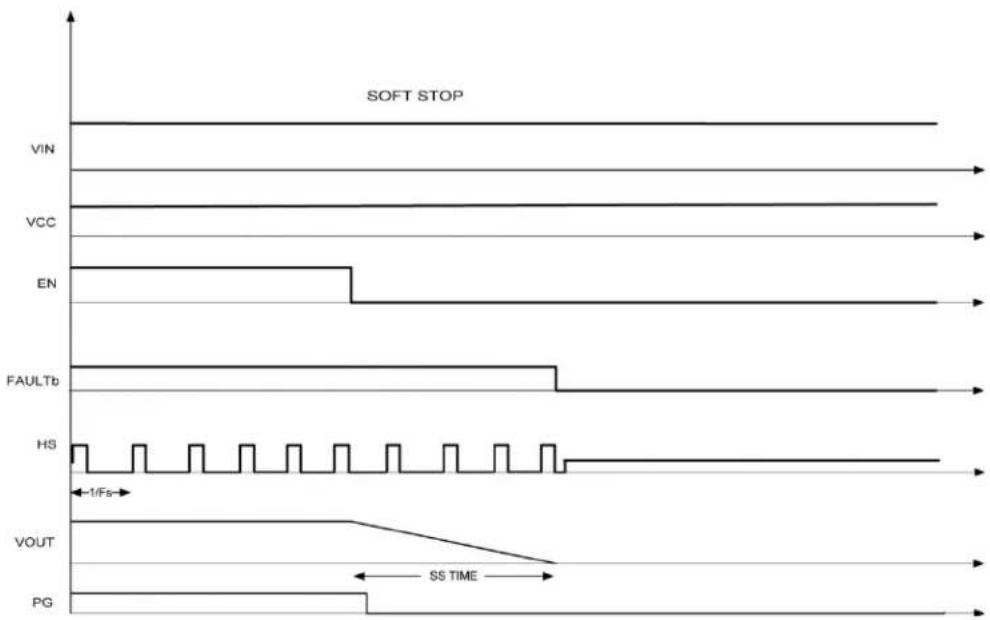
other
| Signal | Time Segment | |--------|--------------| | VIN | 1/Fs | | VCC | 1/Fs | | EN | 1/Fs | | FAULTb | 1/Fs | | HS | 1/Fs | | VOUT | SS TIME | | PG | SS TIME |Figure 5. Typical Soft-Stop
Light Load Operation (DCM)
The MIC2111B supports pulse-skip mode for good light efficiency. Connecting the MODE or SMOD# pin of the power module to GND is required to enable the light-load mode. To avoid discharging the output during light-load mode, the power module zero current detector disables the low-side FET once inductor current reaches zero. The MIC2111B generates the next PWM signal based on COMP voltage. This will cause discontinuous conduction mode at the switch node as shown below.

Figure 6. Light Load Operation (DCM)
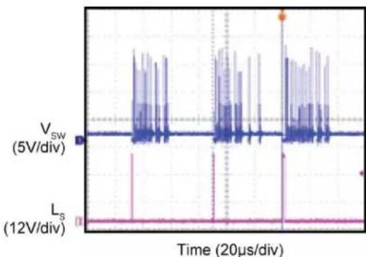
Outside Audio Operation
Some systems require outside audio operation during light-load mode. When the system load reduces during light-load mode, the system will change from CCM to DCM and, as the load reduces further, the switching frequency reduces as well. If the effective switching frequency reduces below a certain threshold, the MIC2111B will enter outside audio mode, attempting to maintain the effective switching frequency above the audio band. For the outside audio mode to function, the LS output of the MIC2111B must be connected to the MODE pin of the DrMOS. While in this mode, if the MIC2111B detects that the period between HS pulses is longer than 32μs it forces LS a logic-1, which turns on the low-side driver. This results in current flowing from the output capacitor through the inductor and low-side MOSFET. This can cause the output voltage to fall and initiate a PWM cycle with HS going high and LS going low.
line
| Time (20μs/div) | V_SW (5V/div) | L_s (12V/div) | | --------------- | ------------- | ------------- | | 0 | 0 | 0 | | 1 | 0 | 0 | | 2 | 0 | 0 | | 3 | 0 | 0 | | 4 | 0 | 0 | | 5 | 0 | 0 | | 6 | 0 | 0 | | 7 | 0 | 0 | | 8 | 0 | 0 | | 9 | 0 | 0 | | 10 | 0 | 0 | | 11 | 0 | 0 | | 12 | 0 | 0 | | 13 | 0 | 0 | | 14 | 0 | 0 | | 15 | 0 | 0 | | 16 | 0 | 0 | | 17 | 0 | 0 | | 18 | 0 | 0 | | 19 | 0 | 0 | | 20 | 0 | 0 |Figure 7. Outside Audio Waveform
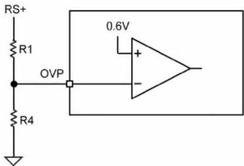
Output Overvoltage Protection (OVP)
The MIC2111B has a dedicated pin for overvoltage protection (OVP). The OVP pin senses the output voltage through a voltage divider. If this voltage is higher than the reference voltage, the overvoltage protection engages and FAULTb is pulled low.
This OVP function typically protects against open feedback loop or V_FB short-to-GND. This will protect the costly load from being damaged by the DC/DC converter.
The OVP level can be programmed through a resistive divider at the OVP pin as follows. Select R4 same as lower feedback resistor. R1 can be calculated based upon required OVP level as illustrated in Equation 1 and Figure 8.
$$ R _ {1} = R _ {4} \times \left[ \frac {\text { OUT } - V \quad V \bar {\theta}}{0 . 6 V} \right]. \tag {Eq.1} $$
text_image
RS+ R1 OVP 0.6V + - R4Figure 8. OVP Programming
After the OVP fault is triggered, the system will be shut down and latched off. It is required to cycle either VCC or EN for enabling the converter.
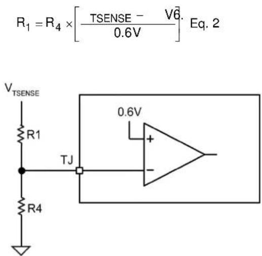
Temperature Sense Input
The MIC2111B has a dedicated input for thermal sense from intelligent power stages. The temperature sense pin (TJ) senses the voltage divided from thermal sense signal and sends it to the comparator. If this voltage is higher than the reference voltage, the thermal shutdown engages and FAULTb is pulled low. Thermal shutdown threshold can be programmed through a resistive divider from TJ.
text_image
R₁ = R₄ × [TSENSE - V6. / 0.6V] Eq. 2 V_TSENSE R1 TJ 0.6V + - R4Figure 9. Thermal-Shutdown Programming
Output will be turned off by pulling FAULTb low after TJ fault is triggered. The fault will be released after hysteresis of 50mV is achieved.
Application Information
Programming Output Voltage with RS Amplifier Diagram
The output voltage is set using a resistive voltage divider from the output of differential amplifier to FB (Figure 10). For R1, use a 1kΩ to 10kΩ resistor. Choose R4 to set the output voltage by using Equation 3.
$$ R _ {4} = R _ {1} \times \left[ \frac {V _ {F B}}{V - V _ {F B Q}} \right] E q. 3 $$
Where V_FB = 0.6V .

text_image
LOAD +SENSE 10Ω RS+ Differential AMPLIFIER A = 1 -SENSE 10Ω RS- VDIFF R1 FB VREF = 0.6V Gm I_RS COMP R4Figure 10. Programming Output Voltage
Current Sensing and Current Limit
MIC2111B has differential current-sense input with a dedicated current-sense amplifier. MIC2111BThe MIC2111B has current-sense amplifier gain of 30V/V and uses lossless inductor current sensing. This offers the advantage of lower power loss and lower cost over using a discrete resistor in series with the inductor.
The inductor sense circuit is shown in Figure 11. It extracts the voltage drop across the inductor's DC winding resistance.

text_image
V_IN OUTPUT INDUCTOR AND WINDING RESISTANCE I_L R_L L R7 C1 30V/V ISEN+ ISEN- C_oFigure 11. MIC2111B Current Sensing
The voltage across capacitor C1 is illustrated in Equation 4:
$$ V _ {S} = I _ {L} \times R _ {L} \left[ \frac {\frac {s L}{R _ {L}} + 1}{\times + 1} \right] E q. 4 $$
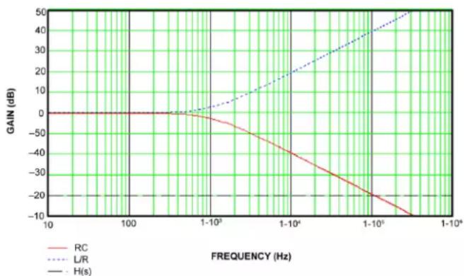
If the R7 x C1 time constant is equal to the L/R L time constant, then the voltage across capacitor C1 equals R L x I L . Figure 12 is a plot of Equation 4. It assumes an inductance of 1.5μH, R L = 0.01Ω (-40dB), C1 = 0.1μF and R7 = 1.5kΩ. The time constants are equal and diverge at the same rate. The overall impedance, H(s), equals R _L for all frequencies.
line
| FREQUENCY (Hz) | RC | L/R | H(s) | | -------------- | ---- | ---- | ---- | | 10 | 0 | 0 | 0 | | 100 | 0 | 0 | 0 | | 1e-3 | -20 | 5 | 0 | | 1e-4 | -40 | 15 | 0 | | 1e-5 | -60 | 30 | 0 | | 1e-6 | -80 | 45 | 0 | | 1e-7 | -100 | 60 | 0 | | 1e-8 | -120 | 75 | 0 | | 1e-9 | -140 | 90 | 0 | | 1e-10 | -160 | 105 | 0 | | 1e-11 | -180 | 120 | 0 | | 1e-12 | -200 | 135 | 0 | | 1e-13 | -220 | 150 | 0 | | 1e-14 | -240 | 165 | 0 | | 1e-15 | -260 | 180 | 0 | | 1e-16 | -280 | 195 | 0 | | 1e-17 | -300 | 210 | 0 | | 1e-18 | -320 | 225 | 0 | | 1e-19 | -340 | 240 | 0 | | 1e-20 | -360 | 255 | 0 | | 1e-21 | -380 | 270 | 0 | | 1e-22 | -400 | 285 | 0 | | 1e-23 | -420 | 300 | 0 | | 1e-24 | -440 | 315 | 0 | | 1e-25 | -460 | 330 | 0 | | 1e-26 | -480 | 345 | 0 | | 1e-27 | -500 | 360 | 0 | | 1e-28 | -520 | 375 | 0 | | 1e-29 | -540 | 390 | 0 | | 1e-30 | -560 | 405 | 0 | | 1e-31 | -580 | 420 | 0 | | 1e-32 | -600 | 435 | 0 | | 1e-33 | -620 | 450 | 0 | | 1e-34 | -640 | 465 | 0 | | 1e-35 | -660 | 480 | 0 | | 1e-36 | -680 | 495 | 0 | | 1e-37 | -700 | 510 | 0 | | 1e-38 | -720 | 525 | 0 | | 1e-39 | -740 | 540 | 0 | | 1e-40 | -760 | 555 | 0 | | 1e-41 | -780 | 570 | 0 | | 1e-42 | -800 | 585 | 0 | | 1e-43 | -820 | 600 | 0 | | 1e-44 | -840 | 615 | 0 | | 1e-45 | -860 | 630 | 0 | | 1e-46 | -880 | 645 | 0 | | 1e-47 | -900 | 660 | 0 | | 1e-48 | -920 | 675 | 0 | | 1e-49 | -940 | 690 | 0 | | 1e-50 | -960 | 705 | 0 | | 1e-51 | -980 | 720 | 0 | | 1e-52 | -1000| | | The data is already in CSV format. It is a simplified representation of the original table. The extracted table contains the frequency values (Hz) and the corresponding gain values (dB) for each table. There are two data series: RC and L/R. The H(s) values are calculated based on the sum of RC and L/R at each frequency point. The data is presented in a tabular format with labels 'RC' and 'L/R'.Figure 12. Current-Sense Gain/Phase Plot
For a system employing the MIC2111B with inductor current sensing, the absolute current-limit threshold is:
$$ I _ {L I M} = \frac {V _ {T H R E S H}}{R _ {D C R}} \tag {Eq.7} $$
Here, R_DCR is the inductor DC resistance. For R_DCR = 1m and a 23.3mV current-limit voltage threshold, the absolute current limit would be:
$$ I _ {L I M} = \frac {V _ {T H R E S H}}{R _ {D C R}} = 0. 0 2 3 3 V / (1 m \Omega) = 2 3. 3 A $$
Eq. 8
For compensating the inductor's DCR variation with temperature, an NTC is placed in parallel with the resistor (R7) in Figure 11.
Slope Compensation
Slope compensation is required in most conditions for current-mode PWM controllers. The MIC2111B applies slope compensation dependent on the system input voltage, output voltage and inductance by a single resistor. The resistor is connected between VIN and the SLOPE pin.
In VCM, 1x slope compensation is implemented by selecting the following resistor value:
$$ R _ {S L O P E} = K _ {S L O P E} \times L / \left[ \left(A _ {I S E N A M P} \times R _ {S E N S E}\right) \right] $$
$$ K _ {S L O P E} = 1. 3 3 \times 1 0 ^ {1 0} \Omega / s $$
$$ L = \text { Inductor value } $$
$$ A _ {I S E N A M P} = \text { Internal current amplifier gain } $$
$$ (3 0 \text { in MIC2111B }) $$
$$ R _ {\text { SENSE }} = \text { External current - sense gain } $$
For low-frequency applications (less than 500kHz) and noisy systems, increasing the slope compensation by a factor of 2 is recommended.
Because slope compensation is not needed in voltage mode, the SLOPE pin is used to generate the sawtooth ramp. A 1V peak-to-peak ramp at the PWM comparator input is implemented by selecting the following resistor value:
$$ R _ {S L O P E} = K \quad S L O P E \times T \times \left(V _ {I N} - V _ {O U T}\right) $$
$$ K _ {\text { S L O P E }} = 1. 3 3 \times 1 0 ^ {1 0} \Omega / \mathrm{s} $$
$$ T = \text { Switching period (1 / switching frequency) } $$
$$ V _ {I N} = \text { System input voltage } $$
$$ V _ {\text { OUT }} = \text { Output voltage } $$
text_image
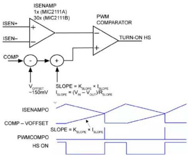
ISENAMP 1x (MIC2111A) 30x (MIC2111B) ISEN+ ISEN- COMP - + PWM COMPARATOR TURN-ON HS V_OFFSET ~150mV SLOPE = K_SLOPE × I_SLOPE I_SLOPE = (V_IN - V_OUT)/R_SLOPE ISENAMPO COMP - VOFFSET SLOPE = K_SLOPE × I_SLOPE PWMCOMPO HS ONFigure 13. Valley Current Mode Compensation
text_image
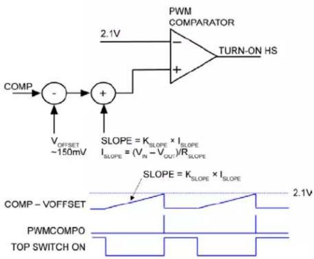
PWM COMPARATOR 2.1V TURN-ON HS COMP - + V_OFFSET ~150mV SLOPE = K_SLOPE × I_SLOPE I_SLOPE = (V_IN - V_OUT)/R_SLOPE COMP - VOFFSET PWMCOMPO TOP SWITCH ON SLOPE = K_SLOPE × I_SLOPE 2.1VFigure 14. Voltage Mode Ramp Generation
Loop Compensation
Current Mode (Type II Method)
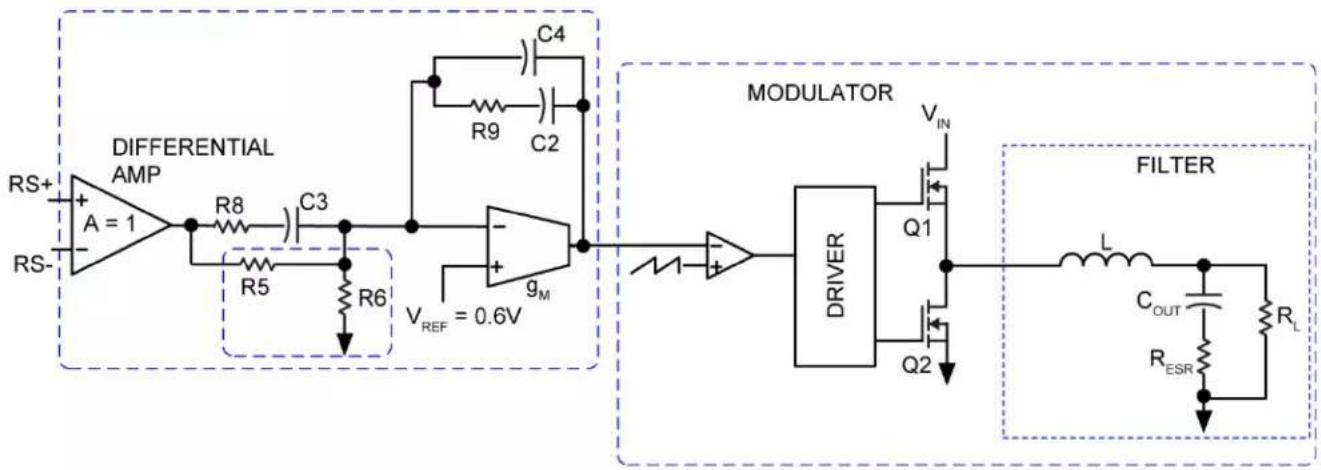
The MIC2111B uses an internal transconductance error amplifier wherein the output compensates the control loop. The external inductor, output capacitor, slope compensation resistor and compensation network all determine the loop stability. The inductor and output capacitors are chosen based on performance, size, and cost. The MIC2111B is configured in a valley current-mode control scheme when the SEL pin is connected to AGND. In this mode, the MIC2111B regulates the output voltage by forcing the required current through the external inductor. Current-mode control eliminates the double pole in the feedback loop which is caused by the inductor and output capacitor. This will result in a smaller phase shift and requires less elaborate error-amplifier compensation than voltage-mode control. A simple series R_c and C_c is all that is needed to have a stable, high-bandwidth loop in applications where ceramic capacitors are used for output filtering. For other types of capacitors, due to the higher capacitance and ESR, the frequency of the zero created by the capacitance and ESR is lower than the desired closed-loop crossover frequency. To stabilize a non-ceramic output-capacitor loop, one would need to add another compensation capacitor from COMP to GND as it cancels this ESR to zero. The basic regulator loop is modeled as a power modulator, an output feedback divider and an error amplifier.
The power modulator has DC gain ( A_MOD(DC) ), is set by R_L , (output load, equivalent resistance) with a pole and zero pair set by R_L , the output capacitor ( C_OUT ) and its equivalent series resistance ( R_ESR ). Equation 9 defines the power modulator (Figure 16)
$$ A _ {\text { MOD(DC) }} = \frac {1}{A _ {\text { CS }}} \frac {R _ {L}}{1 + \frac {R _ {L}}{R _ {\text { SLOPE }}}} \tag {Eq.9} $$
$$ A _ {C S} = A _ {I S E N A M P} \times R _ {S E N S E} $$
As current-mode control separates the complex LC double pole, a pole is formed by load resistance and output capacitance.
$$ \begin{array}{l} f _ {\mathrm{PO}} = \frac {1}{2 \pi \times R _ {\mathrm{L}} \times C _ {\mathrm{OUT}}} \ f _ {Z O} = \frac {1}{2 \pi \times E S R \times C _ {O U T}} \ \end{array} $$
Eq. 10
The feedback voltage-divider has a gain of A_FB = V_FB/V_OUT , where V_FB is equal to 0.6V. The transconductance error amplifier has a DC gain, A_EA(DC) = g_mEA × R_O , where g_mEA is the error-amplifier transconductance, which is equal to 2ms, and R_O is the output resistance of the error amplifier, which is 50MΩ. A dominant pole ( f_pdEA ) is set by the compensation capacitor ( C_C ), the amplifier output resistance ( R_O ), and the compensation resistor ( R_C ); a zero ( f_zEA ) is set by the compensation resistor ( R_C ) and the compensation capacitor ( C_C ). There is an optional pole ( f_pEA ) set by C_Cf and R_C to cancel the output capacitor ESR zero if it occurs near the crossover frequency ( f_C ):
$$ f _ {\mathrm{pdEA}} = \frac {1}{\left(\mathrm{O} \pi \times \mathrm{R} _ {\mathrm{O}} \text {B}\right) \times \mathrm{C} _ {\mathrm{C}}} $$
$$ f _ {z E A} = \frac {1}{2 \pi \times R _ {C} \times C _ {C}} \tag {Eq.11} $$
$$ f _ {\mathrm{pEA}} = \frac {1}{2 \pi \times R _ {\mathrm{C}} \times C _ {\mathrm{C} f}} $$
$$ f _ {\mathrm{pdEA}} = \frac {1}{2 \pi \times (R + R) _ {D} \times C _ {C C}} $$
The crossover frequency, f_O , should be much higher than the power-modulator pole f_PO . Also, f_C should be less than or equal to 1/5 the switching frequency:
$$ _ {\mathrm{PO}} f < _ {\mathrm{O}} f \leq \frac {f _ {\mathrm{SW}}}{5} \tag {Eq.12} $$
Choosing a lower cross-over frequency reduces the effects of noise pickup into the feedback loop, such as jittery duty cycle.
At the crossover frequency, the total loop gain must equal 1, and is expressed as:
$$ \mathrm{A} _ {\text {MOD} (f o)} \times \mathrm{A} _ {\mathrm{EA} (f o)} \times \mathrm{A} _ {\mathrm{FB}} = 1 \tag {Eq.13} $$
Mid-band gain is decided by the g_m and R_C :
$$ \mathsf {A} _ {\mathsf {E A (f o)}} = \mathsf {g} _ {\mathsf {m}} \times \mathsf {R} _ {\mathsf {C}} \tag {Eq.14} $$
Where g_m = 2ms .
$$ \mathsf {A} _ {\mathrm{MOD} (f o)} = \mathsf {A} _ {\mathrm{MOD} (\mathrm{DC})} \times \frac {f _ {\mathrm{PO}}}{f _ {\mathrm{O}}} \tag {Eq.15} $$
Then R_c and C_c can be calculated as:
$$ R _ {C} = \frac {A _ {F B}}{g _ {m} \times A _ {M O D (f _ {O})}} \tag {Eq.16} $$
$$ \mathrm{C} _ {\mathrm{C}} = \frac {1}{2 \pi \times \mathrm{R} _ {\mathrm{C}} \times f _ {\mathrm{PO}}} \tag {Eq.17} $$
For high-current applications, it is recommended to place C_Cf to cancel the effect of ESR zero:
$$ C _ {C f} = \frac {1}{\pi 2 \times C ^ {R \times f _ {P O}}} \tag {Eq.18} $$

flowchart
graph LR
    A["RS+"] --> B["Differential AMP"]
    C["RS-"] --> B
    B --> D["R1"]
    D --> E["R4"]
    E --> F["gM"]
    F --> G["V_REF = 0.6V"]
    G --> H["MODULATOR"]
    H --> I["DRIVER"]
    I --> J["V_IN"]
    I --> K["Q1"]
    I --> L["Q2"]
    I --> M["+"]
    I --> N["+"]
    I --> O["V_IN"]
    I --> P["R_SLOPE"]
    Q["C_CF"] --> R["R_C"]
    R --> S["C_C"]
    T["L"] --> U["R"]
    U --> V["L"]
    W["C_OUT"] --> X["R_L"]
    Y["R_ESR"] --> Z["R_L"]
    style A fill:#f9f,stroke:#333
    style C fill:#f9f,stroke:#333
    style B fill:#ccf,stroke:#333
    style H fill:#cfc,stroke:#333
    style I fill:#fcc,stroke:#333
    style J fill:#cff,stroke:#333
    style K fill:#ffc,stroke:#333
    style L fill:#cfc,stroke:#333
    style M fill:#fcc,stroke:#333
    style N fill:#cfc,stroke:#333
    style O fill:#fcc,stroke:#333
Figure 15. Valley Current Mode Loop Compensation
flowchart
graph TD
    A["RS+"] --> B["Differential AMP"]
    C["RS-"] --> B
    B --> D["R8"]
    D --> E["C3"]
    E --> F["R5"]
    F --> G["R6"]
    G --> H["-"]
    H --> I["9M"]
    I --> J["MODULATOR"]
    J --> K["DRIVER"]
    K --> L["V_IN"]
    L --> M["Q1"]
    M --> N["Q2"]
    N --> O["L"]
    O --> P["C_OUT"]
    P --> Q["R_L"]
    Q --> R["RESR"]
    R --> S["FILTER"]
Figure 16. Voltage Mode Loop Compensation
Equation 22 assumes crossover frequency to be much less than half of the switching frequency. There is a sampling effect at the half switching frequency which introduces the double pole. For high crossover applications, it is recommended to run a bode plot to optimize the transient response.
Voltage Mode (Type III Method)
The MIC2111B provides an internal transconductance amplifier with the inverting input (FB) and the output (COMP) available for external frequency compensation. The flexibility of external compensation allows for a wide selection of output filtering components, especially the output capacitor. The use of high-ESR aluminum electrolytic capacitors is recommended for cost sensitive applications. Use low-ESR POSCAPs or ceramic capacitors at the output for size sensitive applications. The high switching frequency of the MIC2111B allows the use of ceramic capacitors at the output. Choose all passive power components to meet the output ripple, component size, and component cost requirements. Choose the compensation components for the error amplifier to achieve the desired closed-loop bandwidth and phase margin.
To choose the appropriate compensation network type, the power supply poles and zeroes, the zero crossover frequency, and the type of the output capacitor must be determined first.
In a buck converter, the LC filter in the output stage introduces a pair of complex poles at the following frequency:
$$ P D = \frac {1}{\pi \times \sqrt {\times C _ {O U T}} 2} \tag {Eq.19} $$
The output capacitor introduces a zero at:
$$ z f = \frac {1}{\pi 2 R _ {\mathrm{ESR}} \times C _ {\mathrm{OUT}}} \tag {Eq.20} $$
where R_ESR is the equivalent series resistance of the output capacitor.
The loop-gain crossover frequency ( f_O ), where the loop gain equals 1 (0dB) should be set below 1/10^th of the switching frequency as in:
$$ f _ {\mathrm{O}} \leq \frac {f _ {\mathrm{SW}}}{1 0} \tag {Eq.21} $$
Choosing a lower cross-over frequency reduces the effects of noise pick-up into the feedback loop, such as jitter duty cycle.
In order to maintain a stable system, two stability criteria must be met:
-
The phase shift at the cross-over frequency ( f_0 ,) must be less than 180^ . In other words, the phase margin of the loop must be greater than zero.
-
The gain at the frequency where the phase shift is -180^ (gain margin) must be less than 1.
Maintain a phase margin of around 60^ to achieve a robust loop stability and well-behaved transient response.
When using an electrolytic or large-ESR POSCAP output capacitor the capacitor ESR zero (f_ZO) typically occurs between the LC poles and the crossover frequency f_O(f_PO < f_ZO < f_O) . Choose Type II Proportional and Integral (PI) compensation network as previously specified.
When using a ceramic or low-ESR tantalum output capacitor the capacitor ESR zero typically occurs above the desired crossover frequency f_O ( f_PO < f_ZO < f_O ). Choose Type III proportional, integral, and derivative (PID) compensation network.
line
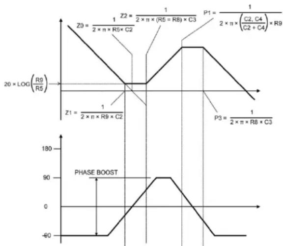
| Phase | Value | |-------|-------| | Z0 | 1/2 × π × R5 × C2 | | Z1 | 1/2 × π × R9 × C2 | | Z2 | 1/2 × π × (R5 = R8) × C3 | | P1 | 1/2 × π × (C2, C4/(C2 + C4)) × R9 | | P3 | 1/2 × π × R8 × C3 |Figure 17. Type III Compensation Pole and Zero Locations
Ensure that R_2 >/g_m and the parallel resistance of R_1 , R_3 , and R_4 is greater than 1/g_M . Otherwise, a 180^ phase shift is introduced to the response making the loop unstable. Use the following compensation procedures:
- With R_9 ≥ 10k , place the first zero ( f_Z1 ) at 0.8 × f_PO :
$$ = f _ {\pi \times} \frac {1}{\times C 2} R 9 ^ {0. 8} 2 ^ {f _ {P O}}; \tag {Eq.22} $$
So,
$$ \mathrm{C} _ {2} = \frac {1}{2 \times R 9 \times 0 . 8 \times f _ {\mathrm{PO}}} \tag {Eq.23} $$
- The gain of the modulator (A _MOD ), comprises the pulse width modulator, LC filter, feedback divider, and associated circuitry at cross-over frequency is:
$$ A _ {\mathrm{MOD}} = \frac {V _ {\mathrm{IN}}}{V _ {\mathrm{RAMP}}} \times \frac {1}{\left(2 \pi \times f _ {\mathrm{O}}\right) ^ {2} \times L _ {\mathrm{OUT}} \times C _ {\mathrm{OUT}}} \quad \text {Eq.24} $$
The gain of the error amplifier ( A_EA ) in mid-band frequencies is:
$$ \mathrm{A} _ {\mathrm{EA}} = 2 \pi \times f _ {\mathrm{O}} \times \mathrm{C3} \times \mathrm{R} _ {9} \tag {Eq.25} $$
The total loop gain as the product of the modulator gain and the error amplifier gain at f_0 is 1:
$$ \mathrm{A} _ {\mathrm{MOD}} \times \mathrm{A} _ {\mathrm{EA}} = 1 \tag {Eq.26} $$
So,
$$ \frac {V _ {\text {IN}}}{V _ {\text {RAMP}}} \times \frac {1}{(2 \pi \times f _ {O}) ^ {2} \times C _ {\text {OUT}} \times L} \times 2 \pi f _ {O} \times C _ {3} \times R 9 = 1 $$
Eq. 27
Solving for C3:
$$ C _ {3} = \frac {V _ {\mathrm{RAMP}} \times (2 \pi \times f _ {\mathrm{O}} \times L \times C _ {\mathrm{OUT}})}{V _ {\mathrm{IN}} \times R _ {9}} \tag {Eq.28} $$
- Use the second pole (f P2 ) to cancel fZO when f_PO < f_O < f_ZO < f_SW/2 . The frequency response of the loop gain does not flatten out soon after the 0dB crossover, and maintains -20dB/decade slope up to 1/2 of the switching frequency. This is likely to occur if the output capacitor is a low-ESR tantalum. Set f_P2 = f_ZO .
When using a ceramic capacitor the capacitor ESR zero f_ZO is likely to be located even above one half of the switching frequency, f_PO < f_O < f_SW/2 < f_ZO . In this case, place the frequency of the second pole ( f_P2 ) high enough in order not to erode significantly the phase margin at the crossover frequency. For example, set f_P2 at 5 × f_O so that the contribution to phase loss at the crossover frequency f_O is only about 11^ :
$$ f _ {\mathrm{P2}} = 5 \times f _ {\mathrm{O}} \tag {Eq.29} $$
Once f_P2 is known, calculate R_1 :
$$ R _ {8} = \frac {1}{2 \pi \times f _ {P 2} \times C _ {3}} \tag {Eq.30} $$
- Place the second zero (f_z2) at 0.2 × f_0 or at f_PO , whichever is lower and calculate R_1 using the following equation:
$$ R _ {5} = \frac {1}{2 \pi \times f _ {Z 2} \times C _ {3}} - R _ {8} \tag {Eq.31} $$
- Place the third pole ( f_P3 ) at 1/2 the switching frequency and calculate C_CF :
$$ \mathrm{C} 4 = \frac {\mathrm{C} _ {2}}{\left(2 \pi \times 0 . 5 \times f _ {\mathrm{SW}} \times \mathrm{R} _ {9} \times \mathrm{C} _ {2}\right) - 1} \tag {Eq.32} $$
- Calculate R_2 as:
$$ R _ {6} = \frac {V _ {F B}}{V _ {O U T} - V _ {F B}} - R _ {5} \tag {Eq.33} $$
Design and Layout Checklist
- Ceramic capacitor placed between the VIN and PGND close to power module input.
- Output ceramic capacitors should be placed next to inductor output node for high-frequency decoupling.
- The signal and power ground planes must be separated to prevent high current and fast switching signals from interfering with the low level, noise sensitive analog signals. These planes should be connected at only 1 point.
- The following signals and their components should be decoupled or referenced to the power ground plane:
- VIN, VCC, PGND
- These analog signals should be referenced or decoupled to the analog ground plane:
– VCC, SS, PG, COMP, FB, VOUT, and AGND
- Place the current-sense lines in differential way. The trace coming from the switch node to this resistor has high dv/dt and should be routed away from other noise sensitive components and traces.
- The remote sense traces must be routed close together or on adjacent layers to minimize noise pickup. The traces should be routed away from the switch node, inductors, and other high dv/dt or di/dt sources.
Typical Application Schematic
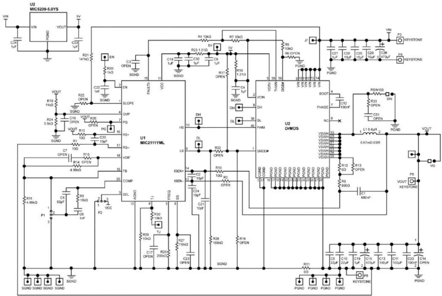
text_image
U2 MIC5209-5.0YS VIN VIN VOUT 5V C34 1μF PGND C33 1μF R21 147kΩ EN R20 1kΩ C22 1nF SGND EN SLOPE OVP PG R19 11kΩ SGND R24 5.5kΩ VOUT R26 OPEN PG R10 10Ω C30 10pF C7 OPEN R15 OPEN 4.99kΩ FB COMP SEL AGND TJ FREQ SS R29 10kΩ C6 1nF P1 3 R11 4.96kΩ C5 82pF R5 10kΩ P2 VCC R30 10kΩ TJ C17 OPEN R25- 200kΩ R27- 118kΩ C23 OPEN R28- 169kΩ SGND R32 OPEN C24 10pF C21 10pF ISEN+ ISEN- LS HS DSL DL ISEN+ ISEN- R4 10kΩ 5V R23 1.21Ω C32 1uF SGND C18 1uF C9 1uF R17 OPEN R18 1.21Ω SGND U1 MIC2111YML FAULTB VCC HCNIN VDRV THWN DISB# VIN VIN VIN VIN VIN VOUT VOUT VOUT VOUT VOUT VOUT VOUT VOUT VOUT VOUT VOUT VOUT VOUT VOUT VOUT VOUT VOUT VOUT VOUT VOUT VOUT VOUT VOUT VOUT VOUT VOUT VOUT VOUT VOUT VOUT VOUT VOUT VOUT VOUT VOUT VOUT VOUT VOUT VOUT VOUT VOUT VOUT VOUT VOUT VOUT VOUT VOUT VOUT VOUT VOUT V OUT V OUT V OUT V OUT V OUT V OUT V OUT V OUT V OUT V OUT V OUT V OUT V OUT V OUT V OUT V OUT V OUT V OUT V OUT V OUT V OUT V OUT V OUT V OUT V OUT V OUT V OUT V OUT V OUT V OUT V OUT V OUT V OUT V OUT V OUT V OUT V OUT V OUT V OUT V OUT V OUT V OUT V OUT V OUT V OUT V OUT V OUT V OUT V OUT V OUT V INN C27 1μF C28 10μF C26 10μF C29 10μF 3 C26 470μF P3 KEYSTONE P4 KEYSTONE P5 RSW Ω SW R33 OPEN C31 OPEN PGND L1 0.4μH 2 0.67mΩ ESR R12 Ω R13 OPEN R8 806Ω C1 680nF C6 22μF C10 22μF C19 1μF C15 470μF C13 100μF C11 100μF C20 100nF C14 OPEN P6 KEYSTONE PGND SGND SGND SGND SGND PGND PGND PGND PGND PGND PGND PGND PGND PGND PGND PGND PGND PGND PGND PGND PGND PGND PGND PGND PGND PGND PGND PGND PGND PGND PGND PGND PGND PGND PGND PGND PGND PGND PGND PGND PGND PGND PGND PGND PGND PGND PGND PGND PGND PGND PGND PGND PGND PGND PGND TG KSTONEBill of Materials
| Item | Part Number | Manufacturer | Description | Qty. |
| C1 | C1608X7R1C684K080AC | TDK^(6) | 0.68μF Ceramic Capacitor, X7R, 0603 Size, 16V | 1 |
| C2, C21, C24, C30 | C1608C0G1H100D | TDK | 10pF Ceramic Capacitor, COG, 0603 Size, 50V | 4 |
| C3, C7, C16, C17, C23, C31, R2, R6, R13, R15, R16, R17, R22, R26 | OPEN | |||
| C4, C9, C18, C19, C27, C32, C33, C34 | C1608X5R1E105K | TDK | 1μF Ceramic Capacitor, X5R, 0603 Size, 25V | 8 |
| C5 | C1608C0G1H820J | TDK | 82pF Ceramic Capacitor, COG, 0603 Size, 50V | 1 |
| C6, C22 | C1608C0G1H102J | TDK | 1nF Ceramic Capacitor, COG, 0603 Size, 50V | 2 |
Note:
6. TDK: www.tdk.com.
Bill of Materials (Continued)
| Item | Part Number | Manufacturer | Description | Qty. |
| C8, C10 | C3225X5R0J226M/1.60 | TDK | 22μF Ceramic Capacitor, X5R,1210 Size,6.3V | 2 |
| C11, C13 | C3225X5R0J107M | TDK | 100μF Ceramic Capacitor, X5R,1210 Size,6.3V | 2 |
| C12, C20 | C1608X7R1E104K | TDK | 100nF Ceramic Capacitor, X7R,0603 Size,25V | 2 |
| C15 | 6SVP470MX | Panasonic^(7) | 470μF OS-CON Capacitor, 6.3V | 1 |
| C25, C28, C29 | C3225X5R1E106M | TDK | 10μF Ceramic Capacitor, X5R,1210 Size, 25V | 2 |
| C26 | EEEFP1E471AP | Panasonic | 470μF Aluminum Capacitor, 25V | 1 |
| L1 | 744325040 | Wurth Electric^(8) | 0.4μH Inductor, 37A Saturation Current | 1 |
| R1, R2, R3, R10 | CRCW060310R0FKEA | Vishay Dale(9) | 10Ω Resistor, 0603 Size, 1% | 4 |
| R4, R5, R7, R9, R29, R30 | CRCW060310K0FKEA | Vishay Dale | 10kΩ Resistor, 0603 Size, 1% | 4 |
| R8 | CRCW0603866RFKEA | Vishay Dale | 866Ω Resistor, 0603 Size, 1% | 1 |
| R11, R14 | CRCW06034K99FKEA | Vishay Dale | 4.99kΩ Resistor, 0603 Size, 1% | 2 |
| R12, R31, RSW | CRCW06030000Z0EA | Vishay Dale | 0Ω Resistor, 0603 Size, 1% | 3 |
| R18, R23 | CRCW06031R21FKEA | Vishay Dale | 1.21Ω Resistor, 0603 Size, 1% | 2 |
| R19 | CRCW060311K0FKEA | Vishay Dale | 11kΩ Resistor, 0603 Size, 1% | 1 |
| R20 | CRCW06031K00FKEA | Vishay Dale | 1kΩ Resistor, 0603 Size, 1% | 1 |
| R21 | CRCW0603147KFKEA | Vishay Dale | 147kΩ Resistor, 0603 Size, 1% | 1 |
| R24 | CRCW06035K49FKEA | Vishay Dale | 5.5kΩ Resistor, 0603 Size, 1% | 1 |
| R25 | CRCW0603200KFKEA | Vishay Dale | 200kΩ Resistor, 0603 Size, 1% | 1 |
| R27 | CRCW0603118KFKEA | Vishay Dale | 118kΩ Resistor, 0603 Size, 1% | 1 |
| R28 | CRCW0603188KFKEA | Vishay Dale | 188kΩ Resistor, 0603 Size, 1% | 1 |
| U1 | MIC2111B | Micrel, Inc.^(10) | High-Performance, Multi-Mode, Step-Down Controller | 1 |
| U2 | SiC769ACD | Vishay Dale | 35A, DrMOS Module | 1 |
| U3 | MIC5209-5.0YS | Micrel Inc. | 500mA, Low-Noise LDO Regulator | 1 |
Notes:
7. Panasonic: www.industrial.panasonic.com.
8. Wurth Electric: www.we-online.com.
9. Vishay Dale: www.vishay.com.
10. Micrel, Inc.: www.micrel.com.
PCB Layout Recommendations
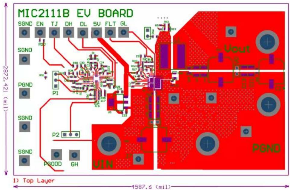
text_image
MIC2111B EV BOARD SGND EN TJ DH DL 5V FLT GL R20 SGND PGND P1 SGND P2 SGND PG00D GH UIN 1) Top Layer 1587.6 (mil) 2872.421 (mil)Top Layer
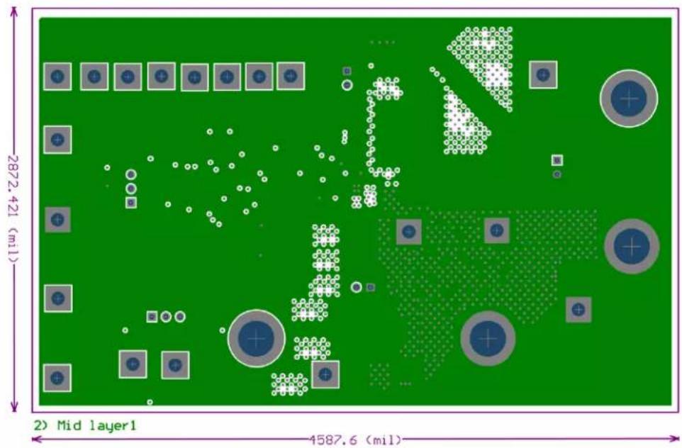
text_image
2872.421 (mil) 2) Mid layer1 4587.6 (mil)Mid Layer 1
PCB Layout Recommendations (Continued)
text_image
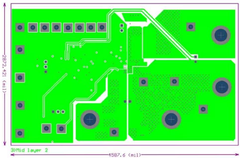
2872.421 (mil) 3)Mid layer 2 4587.6 (mil)Mid Layer 2
text_image
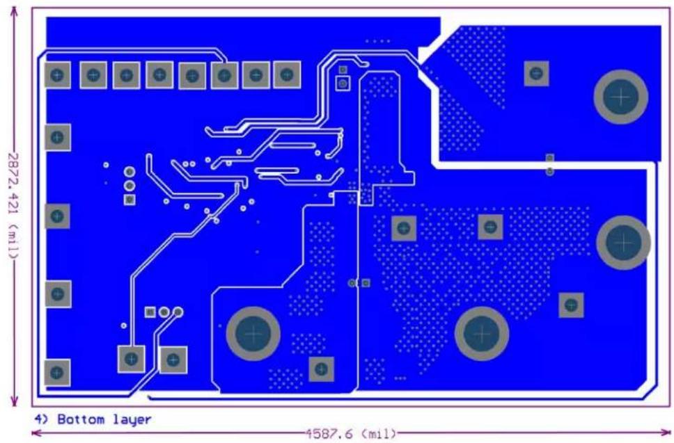
2872.421 (mil) 4) Bottom layer 1587.6 (mil)Bottom Layer 1
Package Information and Recommended Land Pattern ^(11)

text_image
3.0±0.050 3.0±0.050 PIN 1 DOT BY MARKING TOP VIEW NOTE: 1, 2
text_image
0.250±0.050 0.350±0.050 0.500 Bsc 0.800±0.050 0.350±0.050 PIN #1 IDENTIFICATION LL 0.1 BOTTOM VIEW NOTE: 1, 2
text_image
0.550±0.050 0.000-0.050 0.1520 Ref. SIDE VIEW NOTE: 1, 2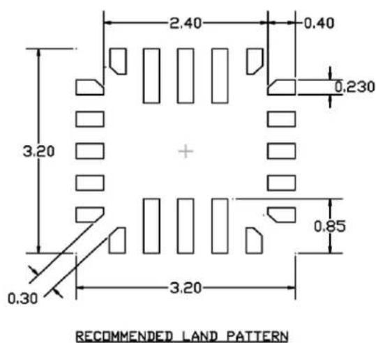
text_image
2.40 0.40 0.230 3.20 + 0.85 3.20 0.30 RECOMMENDED LAND PATTERNNOTE:
1. MAX PACKAGE WARPAGE IS 0.05 MM
2. MAX ALLOWABLE BURR IS 0.076MM IN ALL DIRECTIONS
20-Pin 3mm × 3mm TQFN (MT)
Note:
- Package information is correct as of the publication date. For updates and most current information, go to www.micrel.com.
MICREL, INC. 2180 FORTUNE DRIVE SAN JOSE, CA 95131 USA
TEL +1 (408) 944-0800 FAX +1 (408) 474-1000 WEB http://www.micrel.com
Micrel, Inc. is a leading global manufacturer of IC solutions for the worldwide high-performance linear and power, LAN, and timing & communications markets. The Company's products include advanced mixed-signal, analog & power semiconductors; high-performance communication, clock management, MEMs-based clock oscillators & crystal-less clock generators, Ethernet switches, and physical layer transceiver ICs. Company customers include leading manufacturers of enterprise, consumer, industrial, mobile, telecommunications, automotive, and computer products. Corporation headquarters and state-of-the-art wafer fabrication facilities are located in San Jose, CA, with regional sales and support offices and advanced technology design centers situated throughout the Americas, Europe, and Asia. Additionally, the Company maintains an extensive network of distributors and reps worldwide.
Micrel makes no representations or warranties with respect to the accuracy or completeness of the information furnished in this datasheet. This information is not intended as a warranty and Micrel does not assume responsibility for its use. Micrel reserves the right to change circuitry, specifications and descriptions at any time without notice. No license, whether express, implied, arising by estoppel or otherwise, to any intellectual property rights is granted by this document. Except as provided in Micrel's terms and conditions of sale for such products, Micrel assumes no liability whatsoever, and Micrel disclaims any express or implied warranty relating to the sale and/or use of Micrel products including liability or warranties relating to fitness for a particular purpose, merchantability, or infringement of any patent, copyright, or other intellectual property right.
Micrel Products are not designed or authorized for use as components in life support appliances, devices or systems where malfunction of a product can reasonably be expected to result in personal injury. Life support devices or systems are devices or systems that (a) are intended for surgical implant into the body or (b) support or sustain life, and whose failure to perform can be reasonably expected to result in a significant injury to the user. A Purchaser's use or sale of Micrel Products for use in life support appliances, devices or systems is a Purchaser's own risk and Purchaser agrees to fully indemnify Micrel for any damages resulting from such use or sale.
© 2015 Micrel, Incorporated.