A-188-2 - Synthesizer Doepfer - Free user manual and instructions
Find the device manual for free A-188-2 Doepfer in PDF.

User questions about A-188-2 Doepfer
0 question about this device. Answer the ones you know or ask your own.
Ask a new question about this device
Download the instructions for your Synthesizer in PDF format for free! Find your manual A-188-2 - Doepfer and take your electronic device back in hand. On this page are published all the documents necessary for the use of your device. A-188-2 by Doepfer.
USER MANUAL A-188-2 Doepfer
text_image
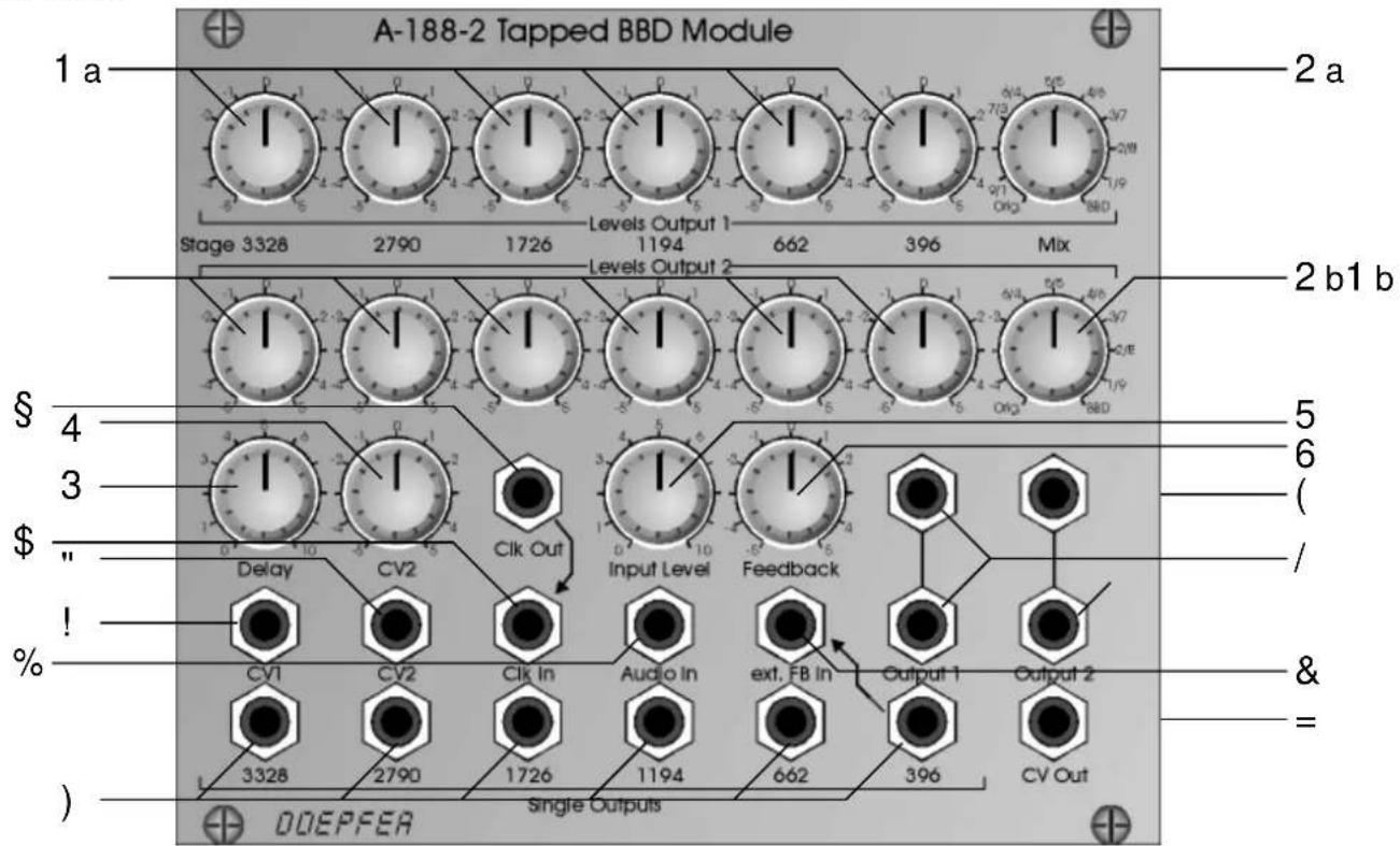
Tapped BBD Module manual CV1 In CV2 In Delay Clock CV Out HSVCO Clock Out Audio In BBD Clock In Feedback In 396 Level 1 662 Level 1 1194 Level 1 1726 Level 1 2790 Level 1 3328 Level 1 Orig./BBD 1 Output 1 396 662 1194 1726 2790 3328 Output 2 Tap OutputsFig. 1: A-188-2 Controls and In/Outputs
1. Introduction
Module A-188-2 based on a so-called Bucket Brigade Device (abbr. BBD). In contrast to the A-188-1 the A-188-2 uses a tapped BBD circuit, i.e. the circuit has available six different outputs at the BBD stages 396, 662, 1194, 1726, 2790 and 3328. Each of the taps is available as a single output but the module features also two mixing sub-units. For both mixers the levels and polarities of each BBD output can be adjusted to obtain two different mixtures. Each mixer has a wet/dry control that allows choosing between the original signal, the BBD mix or anything in between. The outputs can be treated as stereo outputs but that's not . Due to the six taps even six different feedback types are possible. The feedback input socket is normalled to the "396" output. But by patching the feedback socket to any of the single output sockets another BBD tap can be used for positive or negative feedback to obtain different sounds. Even external feedback processing is possible. The A-188-2 uses a high speed VCO to generate the BBD clock. The clock and consequently the delay time can be controlled manually and by the two control voltage inputs CV1 and CV2. CV2 is equipped with a polarizer. The module has a clock output available that is normalled to the clock input socket. These sockets can be used to link different BBD modules and to run them with the same clock. A voltage composed of the manual delay control, CV1 and CV2 is available at the CV out socket, e.g. to control an external clock suppression filter as the A-188-2 is not equipped with such a filter.
2. Basic Principles
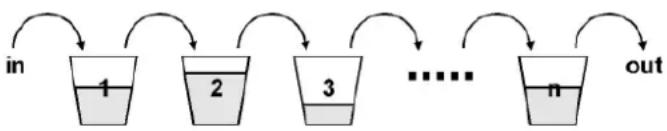
A BBD circuit can be regarded as a chain of Sample & Hold units (S&H) which pass on their voltages to the next S&H in the chain at each clock pulse. From this also the name Bucket Brigade Device is derived as each stage of the BBD can be treated as a bucket. At each clock pulse the content of each bucket is forwarded to the next bucket in the chain and the current bucket is filled with the contents of the preceding bucket.
flowchart
graph LR
    A["in"] --> B["1"]
    B --> C["2"]
    C --> D["3"]
    D --> E["..."]
    E --> F["n"]
    F --> G["out"]
Fig.2: Bucket Brigade
Remark: In reality two "buckets" are required for each stage as the content of a bucket has to be stored temporarily in a "slave bucket" before it can be filled with the contents of the preceding bucket, in contrast to a "real" bucket brigade not the buckets are passed on but only the contents.
In the BBD the water is replaced by analog voltages which again represent audio signals. The first bucket (1) is the audio input, the last bucket (n) is the output of the BBD. As in reality there are losses while the water (resp.
(voltage) is passed on, because some drops of water go wrong and at the end of the chain not the same amount of water (resp. not exactly the same voltage) appears. In a BBD the buckets are replaced by capacitors and analog switches. As the capacitors of a BBD are very small (some pF only) even the time required to pass on the input to the output is crucial as the capacitors loose their charges if it takes too long. This is why a minimum clock frequency is specified for each BBC circuit. Below this frequency the flawless operation of a BBD is not guaranteed. In the A-188-2 intentionally frequencies can be used that go below this value to obtain special "dirty" and "crunchy" effects.
Standard BBD circuits as described above are available (or rather have been available) with different numbers of stages. Usual numbers are 128, 256, 512, 1024, 2048 or 4096 stages. In the A-188-2 a very special BBD circuit with 3328 stages is used (MN3011) that is equipped with additional outputs (taps) at the stages 396, 662, 1194, 1726 and 2790.
The number of stages defines the delay time that corresponds to a certain clock frequency. The higher the number of stages, the longer is the delay. The higher the clock frequency, the shorter is the delay.
Example: At 100kHz clock frequency the delay time is 10.24 ms for a BBD with 1024 stages and 20.48 ms for a BBD with 2048 stages.
The following table shows the relation between clock frequency, used output stage (tap) and delay time for the BBD circuit used in the A-188-2 (MN3011).
Table 1: Relation between clock frequency [kHz], used output (tap) and delay time [ms]
| clock frequency (clock input socket) | BBD clock frequency (= 1/2 clock input) | MN3011 tap/stage output | |||||
| [kHz] | [kHz] | 396 | 662 | 1194 | 1726 | 2790 | 3328 |
| 1 | 0,5 | 396,00 | 662,00 | 1194,00 | 1726,00 | 2790,00 | 3328,00 |
| 2 | 1 | 198,00 | 331,00 | 597,00 | 863,00 | 1395,00 | 1664,00 |
| 5 | 2,5 | 79,20 | 132,40 | 238,80 | 345,20 | 558,00 | 665,60 |
| 10 | 5 | 39,60 | 66,20 | 119,40 | 172,60 | 279,00 | 332,80 |
| 20 | 10 | 19,80 | 33,10 | 59,70 | 86,30 | 139,50 | 166,40 |
| 50 | 25 | 7,92 | 13,24 | 23,88 | 34,52 | 55,80 | 66,56 |
| 100 | 50 | 3,96 | 6,62 | 11,94 | 17,26 | 27,90 | 33,28 |
| 200 | 100 | 1,98 | 3,31 | 5,97 | 8,63 | 13,95 | 16,64 |
| 300 | 150 | 1,32 | 2,21 | 3,98 | 5,75 | 9,30 | 11,09 |
| 400 | 200 | 0,99 | 1,66 | 2,99 | 4,32 | 6,98 | 8,32 |
| 500 | 250 | 0,79 | 1,32 | 2,39 | 3,45 | 5,58 | 6,66 |
Remarks:
The grey italic characters indicate parameters out of the data sheet specifications as the MN3011 circuit is specified only for clock frequencies between 10kHz and 100kHz. But the A-188-2 is able to generate even clock frequencies below 10kHz and above 100kHz. From our experience the MN3011 cannot be damaged if it is operated with frequencies out of spec. This is why we decided to include out-of-spec frequencies to obtain special audio effects – especially for clock frequencies below 10kHz. But the regular circuit behaviour is no longer guaranteed (especially increasing voltage losses at lower frequencies). As the clock frequency falls below \~ 15 kHz the clock signal itself will become audible. This clock noise can be used as unusual audio source or it can be filtered out with an external low pass filter.

flowchart
graph TD
    A["audio level"] --> B["adder"]
    B --> C["Tapped BBD Circuit"]
    C --> D["adder"]
    D --> E["BBD Mix 1"]
    D --> F["Original"]
    F --> G["BBD Mix 2"]
    H["ext. clock in"] --> I["2-phase converter"]
    I --> J["manual + CV1 + CV2"]
    J --> K["high speed VCO"]
    K --> L["CV1"]
    K --> M["CV2"]
    N["single outputs"] --> O["adder"]
    O --> P["BBD Mix 1"]
    O --> Q["Original"]
    R["feedback level/pol."] --> S["adder"]
    S --> T["BBD Mix 1"]
    S --> U["Original"]
    V["Out 1"] --> W["Back to Adder"]
    X["Out 2"] --> Y["Back to Adder"]
Fig. 3: A-188-2 module scheme
Fig. 3 shows the internal circuit details of the module: the upper part is the high speed VCO (HSVCO), the lower part the actual BBD section.
The HSVCO generates the clock signal that is required to drive the BBD. It has available a manual control and two CV inputs. CV1 is without attenuator and follows approximately the 1V/octave standard (for precision 1V/octave applications an external precision HSVCO is required). CV2 is equipped with a polarizer.
Polarizer function: In the center position of the polarizer control the effect of the control voltage applied to the socket CV2 is zero. Turning the knob clockwise from the center position the control voltage effect becomes positive with increasing amount. Turning the knob counterclockwise from the center position the control voltage effect becomes negative with increasing amount.
The HSVCO has a CV output available that corresponds to the sum of all CVs that define the HSVCO's frequency, i.e. the manual control, CV1 and CV2. It's main purpose is to control the CV input of external low pass filter(s) that can be used as anti-aliasing filter and clock filter. If desired a low pass filter can be used behind the audio output(s) to suppress the clock noise when the clock frequency falls below \~15 kHz. Another filter can be used at the audio input to reduce the max. frequency of the incoming audio signal, consequently reducing aliasing artefacts. As the CV output reflects the clock frequency (affected by the manual control, CV1 and CV2) the external filters automatically follow the clock frequency of the BBD module. The higher the slope of the external filter (e.g. 12/24/48 dB/octave) the better is the clock suppression. The HSVCO features also a clock output that can be used e.g. to synchronize two A-188-2 or an A-188-2 and A-188-1 (i.e. both BBD modules use the same clock source) or as high speed clock for other applications (e.g. graphic VCO, switched capacitor filter).
The clock output of the HSVCO is normalled to the clock input of the BBD section. The clock input makes it possible to control the BBD by an external clock source (e.g. another A-188-2 or A-188-1 or any other clock signal in the required frequency range). For all clock signals from and to the A-188-1/2 only short patch cables should be used, as long cables function as low pass filters for signals above 20kHz.
A two-phase converter generates the two opposite clock signals that are required to drive the BBD circuits.
The audio input of the BBD module is equipped with an attenuator that enables to reduce the input level to avoid distortion. The audio input signal behind the attenuator is mixed with the feedback signal (details below) and fed to the audio input of the BBD circuit.
Each tap of the BBD circuit is available as a single output: 396, 662, 1194, 1726, 2790 and 3328. These outputs can be used for example in an additional external (e.g. voltage controlled) mixer or for multi-channel applications (e.g. 5.1).
Each tap is connected to two polarizers (the polarizer function is described on the last page). One of the polarizers is assigned to the sub-mixer 1, the second to sub-mixer 2. The sub-mixers are labelled adder with the sign (sum) in the module scheme. The reason for the polarizers instead of simple attenuators is that the polarity of each tap is crucial for the output mixing (for both tap output + original signal and even for the taps among each other).
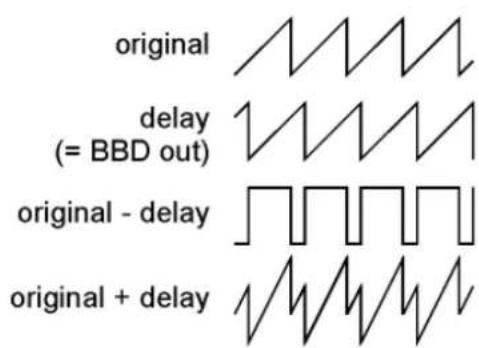
The following sketch shows the difference between adding and subtracting one tap output to/from the original signal by means of a simple sawtooth signal as audio input.
text_image
original delay (= BBD out) original - delay original + delayFig. 4: positive/negative mixing of original and BBD signal
The two sub-mixers are used to mix the outputs of the six BBD taps with adjustable levels and polarities. Each sub-mixer has available wet/dry control to adjust the relation between the original and the effect signal. The effect signal is the sum of the tap outputs.
The A-188-2 features a feedback section that is very similar to the one in the A-188-1. But as now six different BBD outputs are available even six different feedback types are possible. The feedback input socket is normalled to the 396 output. But by patching the feedback socket to any of the other single output sockets another BBD tap can be used for the feedback to a obtain different sound. Even external feedback processing is possible (e.g. a VCA or a VC polarizer for voltage controlled feedback, or other modules like filter, phaser, frequency shifter, waveshaper, wave multiplier, ring modulator or another BBD module for special voltage controlled feedback effects). The feedback control has polarizer function, i.e. the neutral position is at the center. Left from the center the feedback signal is subtracted from the input signal, right from the center it's added (negative/positive feedback). The polarity of the feedback signal leads to clearly audible different sounds as different frequencies are emphasized or attenuated for positive or negative feedback.
The feedback can be increased up to self-oscillation. In contrast to other feedbacks (e.g. filters or phasers) the result in the self-oscillation state depends upon the "audio history" (i.e. the contents of the BBD when the self-oscillation is triggered). The reason is that there is not only one possible stable self-resonant state for the BBD. Any cyclic waveform "stored" in the BBD is able to resonate provided that the feedback maintains the waveform. One can try this out e.g. with different audio signals (e.g. digital noise and VCO sawtooth) as audio input before self-oscillation is triggered.
A special feedback can be obtained if one of the sub-mixer outputs is used for the feedback function. In this case for each tap the positive or negative feedback share can be adjusted. This leads to multiple peaks and/or notches in the frequency response of the module.
- Overview
text_image
A-188-2 Tapped BBD Module Stage 3328 2790 1726 Levels Output 1 1194 662 396 Mix Levels Output 2 2 a 2 b1 b $ 4 3 $ " ! % ) ODEPFEA Single Outputs Delay CV2 Clk Out Input Level Feedback CV1 CV2 Clk In Audio In ext. FB In Output 1 Output 2 3328 2790 1726 1194 662 396 CV OutFig.5: A-188-2 front panel
Note: The labelling of the output sockets is wrong. The left pair of sockets is Output 2, the right pair is Output 1
Controls:
1 a, 1 b : mix levels/polarities of the BBD taps
3328, 2790, 1726, 1194, 662 and 396
(polarizers)
2 a, 2 b Mix: wet/dry controls for outputs 1 and 2
(1 /2 a are assigned to sub-mixer 1)
1 /2 b are assigned to sub-mixer 2)
3 Delay : manual delay/clock control
4 CV2: attenuator for CV2
5 Input Level: audio input attenuator
6 Feedback: feedback level and polarity control (polarizer)
In- / Outputs:
! CV1: CV1 input HSVCO
" CV2: CV2 input HSVCO
§ Clk Out: clock output HSVCO
\$ Clk In: BBD clock input
(normalled to Clock Out § )
% Audio In: audio input
& Ext.FB In: external feedback input
(normalled to BBD Out) 396)
/ Output 1: mixed audio output 1
( Output 2: mixed audio output 2
) Single outputs: single audio outputs of the taps
3328, 2790, 1726, 1194, 662 and 396
= CV Out: CV output HSVCO
Note: The labelling of the output sockets is wrong. The left pair of sockets is Output 2, the right pair is Output 1
4. Controls and In- / Outputs
4.1. High Speed VCO Section
3 Delay : manual delay/clock control
! CV1: CV1 input HSVCO
" CV2: CV2 input HSVCO
4 CV2: attenuator for CV2
§ Clk Out: clock output HSVCO
= CV Out: CV output HSVCO
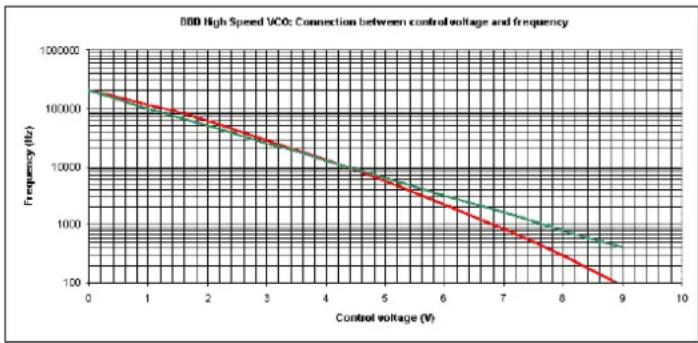
This group of elements is responsible for the clock frequency generated by the high speed VCO (HSVCO). knob 3 Delay Clock is used to adjust the clock manually. Two CV inputs (! CV1, " CV2) are available to control the clock by external control voltages (e.g. LFO, envelope follower, random, ADSR, keyboard CV, sequencer, theremin, ribbon controller, foot controller, Midi-to-CV, shepard generator ...). The sensitivity of CV1 is approximately 1V/octave. The diagram on the right side shows the connection between CV1 and clock frequency. The straight line represents the perfect 1V/oct graph. The slightly bended curve is the real behaviour of the HSVCO. If an absolutely "perfect" 1V/octave control is required an external precision HSVCO or a VCO with PLL has to be used.
The second control voltage input " CV2 is equipped with a polarizer. The function of a polarizer is described on page 5.
line
83D High Speed VCO: Connection between control voltage and frequency | Control voltage (V) | Frequency (Hz) | | :--- | :--- | | 0 | 100000 | | 1 | 50000 | | 2 | 25000 | | 3 | 12500 | | 4 | 6250 | | 5 | 3125 | | 6 | 1562 | | 7 | 781 | | 8 | 390 | | 9 | 195 | | 10 | 97 |Fig 6: relation between CV1 and Clock Frequency
§ Clk Out: clock output HSVCO
This is the clock output of the HSVCO. It is internally connected to the clock input of the BBD section. The waveform is rectangle with about ± 3V level. The rectangle slopes flatten with increasing frequency and the waveform turns more and more into triangle. Even the load on the output has influence to the waveform and level. Consequently for all clock patches from and to the A-188-2 only short patch cables ( 30 cm) should be used because long cables function as low pass filters for signals above 20kHz. The max. frequency at this output is about 250 kHz.
= CV Out: CV output HSVCO
This CV output indicates the clock frequency at output § and is nothing but the sum of all CV inputs (manual, CV1 and CV2). The main purpose of this output is to control the CV input of external low pass filters that can be used as anti-aliasing filter and clock filter. If desired one low pass filter can be used behind the audio output to suppress the clock noise, especially when the clock frequency falls below \~15 khz. Another filter can be used at the audio input to reduce the max. frequency of the incoming audio signal, consequently reducing aliasing artefacts. As the CV output reflects the clock frequency (affected by the manual control, CV1 and CV2) the external filters automatically follow the clock frequency of the BBD module. The higher the slope of the external filter (e.g. 12/24/48 dB/octave) the better is the clock suppression. But the CV output can be used for other applications as well, e.g. controlling parameters of the feedback loop like feedback amount/polarity (CV of a VCA or VC polarizer used in the feedback loop), filter frequency (CV of a VCF used in the feedback loop), phase shift (CV of a VC phaser used in the feedback loop).
4.2. BBD and Sub-Mixer Section
This is the clock input of the BBD section and is internally connected to the clock output § of the HSVCO section (i.e. it is normalled to the Clock Out socket §). If an external clock source is used the clock output of this source is patched to socket \$. In this case the internal connection to the HSVCO is interrupted. The clock frequency table can be found on page 3. The required level for the clock signal is about +3V (levels up to +12V cause no problems). This socket can be used e.g. to synchronize two A-188-2 modules or an A-188-2 and A-188-1 (i.e. using one HSVCO for both modules).
Sockets % is the audio input with the assigned attenuator 5. Feed the audio signal that has to be processed by the A-188-2 into socket %. Adjust the Level control 5 so that the output signal does not distort - unless you want to obtain distortion. For normal A-100 levels (e.g. VCO A-110) distortion appears at about three o'clock position of control 5.
) Single Outputs
The six sockets ) are the "raw" outputs (taps) of the BBD stages 3328, 2790, 1726, 1194, 662 and 396. These outputs can be used e.g. for feedback patching, for external mixing (e.g. with a voltage controlled mixer) or for multi-channel applications (e.g. 5.1 sounds).
1 a, 1 b : mix levels/polarities of the BBD taps
3328, 2790, 1726, 1194, 662 and 396
(polarizers)
2 a, 2 b Mix: wet/dry controls for outputs 1 and 2
(1 /2 a are assigned to sub-mixer 1)
1 /2 b are assigned to sub-mixer 2)
/ Output 1: mixed audio output 1
( Output 2: mixed audio output 2
This group of elements is responsible for the two mixed outputs appearing at the sockets / Output 1 and (Output 2. In the left/ccw position of the knobs 2 a/b Mix the original signal appears at the sockets / /( . In the right/cw position of the knobs 2 a/b Mix the internal pre-mix signal composed from the six BBD taps with the polarizers 1 a/b appears at the sockets / /( . In the intermediate positions of the knobs 2 a/b Mix a mix of these two signals appears at the corresponding output socket.
Note: The labelling of the output sockets is wrong. The left pair of sockets is Output 2, the right pair is Output 1
& Ext.FB In: external feedback input
6 Feedback: feedback level and polarity control (polarizer)
This group of elements is responsible for the feedback functions of the module. Socket & Ext.FB In is the input of the feedback loop and is normalled to socket) BBD Out 396. Patching the feedback socket to any of the other single output sockets another BBD tap can be used for the feedback function to a obtain different sound. If an external module is used to control the feedback loop (e.g. a VCA or VC polarizer) the module has to be inserted between one of the six sockets) BBD Out and socket & Ext.FB In. The feedback control 6 Feedback is a polarizer with the neutral position at the center. Left from the center the feedback signal is subtracted from the input signal, right from the center it's added (negative/positive feedback). The polarity of the feedback signal leads to clearly audible different sounds especially at short delay times as different frequencies are emphasized or attenuated for positive or negative feedback. For longer delay times ("analog delay" application) the sound differences are much smaller
In the fully right/cw or fully left/ccw position of the feedback control 6 the module goes into self-oscillation. As already mentioned in chapter 2 the result in the self-oscillation state depends upon the "audio history" (for details please refer to page 7).
5. User Examples
text_image
A-145 UFO A-188-2 Tapped BBD Module Voltage 300V 1.75V Ground Output 1 Ground Output 2 Output 3 Output 4 Output 5 Output 6 Output 7 Output 8 Output 9 Output 10 Output 11 Output 12 Output 13 Output 14 Output 15 Output 16 Output 17 Output 18 Output 19 Output 20 Output 21 Output 22 Output 23 Output 24 Output 25 Output 26 Output 27 Output 28 Output 29 Output 30 Output 31 Output 32 Output 33 Output 34 Output 35 Output 36 Output 37 Output 38 Output 39 Output 40 Output 41 Output 42 Output 43 Output 44 Output 45 Output 46 Output 47 Output 48 Output 49 Output 50 Output 51 Output 52 Output 53 Output 54 Output 55 Output 56 Output 57 Output 58 Output 59 Output 60 Output 61 Output 62 Output 63 Output 64 Output 65 Output 66 Output 67 Output 68 Output 69 Output 70 Output 71 Output 72 Output 73 Output 74 Output 75 Output 76 Output 77 Output 78 Output 79 Output 80 Output 81 Output 82 Output 83 Output 84 Output 85 Output 86 Output 87 Output 88 Output 89 Output 90 Output 91 Output 92 Output 93 Output 94 Output 95 Output 96 Output 97 Output 98 Output 99 Output 100Standard Modulation Patch
Suitable control voltage sources are LFO (A-145 as shown in the example, A-146, A-147, A-143-3), random voltage (A-118, A-149-1), envelopes (A-140, A-141, A-142, A-143-1, A-143-2), S&H (A-148, A-152), sequencer (A-155), theremin (A-178) or ribbon controller (A-198).
Even for the "enveloped BBD" patch with the envelope follower of the A-119 as control voltage the A-188-2 can be used (described in the user's manual of the A-188-1 on page 13).

text_image
A-133 POL Dual VC Podulator A-188-2 Tapped B8D Module RV CV RV RV RV RV RV RV RV RV RV RV RV RV RV RV RV RV RV RV RV RV RV RV RV RV RV RV RV RV RV RV RV RV RV RV RV RV RV RV RV RV RV RV RV RV RV RV RV RV RV RV DV In DV In DV In DV In DV In DV In DV In DV In DV In DV In DV In DV In DV In DV In DV In DV In DV In DV In DV In DV In DV In DV In DV In DV In DV In DV In DV In DV In DV In DV In DV In DV In DV In DV InVoltage Controlled Feedback
The feedback is processed by an external voltage controlled polarizer (A-133) to obtain voltage controlled feedback. Instead of the polarizer even a VCA can be used. But with a VCA only positive or negative feedback is possible. Any of the single outputs of the A-188-2 can be used for the feedback loop. Even other sound processing modules (e.g. filters, frequency shifter, wave multiplier, spring reverb, phaser) can be used for voltage controlled feedback processing.

text_image
A-188-2 Tapped 8BD Module A-108 VCD Audio Out Output 60 60 40 30 20 10 0 Audio In Audio Level Audio Audio Out Single/Outset 1706 1704 AV2 AV2 AV2 AV2 AV2 AV2 AV2 AV2 AV2 AV2 AV2 AV2 AV2 AV2 AV2 AV2 AV2 AV2 AV2 AV2 AV2 AV2 AV2 AV2 AV2 AV2 AV2 AV2 AV2 AV2 AV2 AV2 AV2 AV2Clock Filter
The BBD audio output is filtered by a low pass (e.g. A-108). The frequency of the low pass filter follows the BBD clock frequency as the CV output of the module A-188-2 is used to control the frequency of the low pass filter. If both outputs have to be filtered another low pass is required for the second output.
An additional filter can be used at the audio input of the A-188-2 to limit the frequency range of the processed audio input signal.

text_image
A-152 Address KeySwitch A-164.0 Capped BCD Module CV In Clock In Audio Out 1 Audio Out 2 Audio InClocked or voltage controlled feedback type
The single outputs of the A-188-2 are patched to the inputs of the addressed switch A-152. The common output of the A-152 is patched to the feedback input of the A-188-2. The CV or the clock input of the A-152 is used to switch between different feedback types. If a sequencer is used for each step of the sequence another feedback type can be chosen. The digital output #7 of the A-152 is connected to the reset input to limit the number of used steps to six.
text_image
A-166-2 Tapped BDO Module A-135-1 VCMX VOLTAGE CONTROL/ALDINASES CV1 In CV2 In CV3 In CV4 In Audio Out Audio In Single Output 00EPPER 00EPPERVoltage controlled output mixing
Four of the single outputs of the A-188-2 are patched to the audio inputs of a voltage controlled mixer A-135-1. The four control voltages of the A-135-1 are used to define the levels of the BBD taps.
Even the Karplus/Strong patches described in the A-188-1 user's manual can be realized with the A-188-2. The mixed outputs of the A-188-2 lead to more complex sounds compared to the A-188-1.
DOEPFER
System A-100
BBD Module A-188-2