
EUR7659T40 - Remote control PANASONIC - Free user manual and instructions
Find the device manual for free EUR7659T40 PANASONIC in PDF.


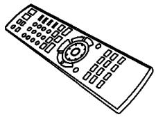
| Product type | Infrared remote control |
| Brand | PANASONIC |
| Model | EUR7659T40 |
| Compatibility | Panasonic DVD recorders DMR-EX75EG/EX75EB/EX75EC/EX85EG/EX85EB |
| Dimensions | Approximately 160 x 50 x 25 mm |
| Weight | Approximately 100 g (without batteries) |
| Power supply | 2 AAA batteries (1.5 V) not included |
| Range | Approximately 7 meters |
| Operating angle | ±30° relative to the receiver axis |
| Main functions | Control of DVD, HDD and SD players; menu navigation; playback, recording, timer settings; TV functions (on/off, volume, channels) |
| Care and cleaning | Clean with a soft, dry cloth. Do not use solvents or abrasive cleaners. |
| Safety | Avoid exposure to humidity, extreme temperatures, and impacts. Do not open or attempt to repair. |
| Spare parts and repairability | Only the batteries are user-replaceable. In case of malfunction, contact an authorized service center. |
| General information | Original Panasonic remote control, designed for use with DMR-EX75/EX85 series DVD recorders. |
Frequently Asked Questions - EUR7659T40 PANASONIC
User questions about EUR7659T40 PANASONIC
0 question about this device. Answer the ones you know or ask your own.
Ask a new question about this device
Download the instructions for your Remote control in PDF format for free! Find your manual EUR7659T40 - PANASONIC and take your electronic device back in hand. On this page are published all the documents necessary for the use of your device. EUR7659T40 by PANASONIC.
USER MANUAL EUR7659T40 PANASONIC
DMR-EX75EG
DMR-EX75EB
DMR-EX75EC
DMR-EX85EG
DMR-EX85EB
EUR7659YM0
EUR7659YG0
EUR7659T40
EUR7659YM0
EUR7659YG0
DMR-EX75EG
DMR-EX75EC
DMR-EX75EB
DMR-EX85EG
DMR-EX85EB
Vol.1
Colour
(S)......Silver Type
NOTES:
This model's RAM / Digital P.C.B.
Module are - RFKNEX75EG
- RFKNEX75EB
- RFKNEX75EC
- RFKNEX85EG
- RFKNEX85EB
CAUTION:
Pairing of RAM Drive and Digital P.C.B. as "RAM / DIGITAL P.C.B. MODULE" have to be replaced together. If the pairing is changed, RAM Drive unit has to be re-aligned. Because the alignment data for RAM Drive Unit is stored in Digital P.C.B.
Manufactured under license from Dolby Laboratories. "Dolby" and double-D symbol are trademarks of Dolby Laboratories.
"DTS" and "DTS 2.0 + Digital Out" are trademarks of Digital Theater Systems, Inc.
• SD logo is a trademark. - Portions of this product are protected under copyright law and are provided under license by ARIS/SOLANA/4C. - miniSD™ is a trademark of SD Card Association.
Apparatus Claims of U.S. Patent Nos. 4,631,603, 4,577,216, and 4,819,098, licensed for limited viewing uses only.
HDAVI Control™ is a trademark of Matsushita Electric Industrial Co., Ltd.
G-CODE is a registered trademark of Gemstar Development Corporation. The G-CODE system is manufactured under license from Gemstar Development Corporation.
When replacing with Main P.C.B. or EEPROM, "UNFORMAT" indication is displayed and HDD must be formatted.
When replacing with HDD it is necessary to update the firmware. Please prepare the update disc. (After that, FORMAT is necessary)
After that, programme in the HDD will be lost. In detail, please refer to each content in this service manual.
HDMI, the HDMI logo and High-Definition Multimedia Interface are trademarks or registered trademarks of HDMI Licensing LLC.
MPEG Layer-3 audio decoding technology licensed from Fraunhofer IIS and Thomson multimedia.
This product incorporates copyright protection technology that is protected by method claims of certain U.S. patents and other intellectual property rights owned by Macrovision Corporation and other rights owners. Use of this copyright protection technology must be authorized by Macrovision Corporation, and is intended for home and other limited viewing uses only unless otherwise authorized by Macrovision Corporation. Reverse engineering or disassembly is prohibited.
Official DivX Certified™ product.
Plays DivX®5, DivX®4, Div®3, and Div® VOD video content (in compliance with DivX Certified™ technical requirements). DivX, DivX Certified, and associated logos are trademarks of DivXNetworks, Inc. and are used under license.

WARNING
This service information is designed for experienced repair technicians only and is not designed for use by the general public. It does not contain warnings or cautions to advise non-technical individuals of potential dangers in attempting to service a product. Products powered by electricity should be serviced or repaired only by experienced professional technicians. Any attempt to service or repair the product or products dealt with in this service information by anyone else could result in serious injury or death.
CONTENTS
Page
1 SAFETY PRECAUTIONS 3
1.1. GENERAL GUIDELINES 3
2 WARNING 4
2.1. PREVENTION OF ELECTROSTATIC DISCHARGE (ESD) TO ELECTROSTATIC SENSITIVE (ES) DEVICES-4
2.2. PRECAUTION OF LASER DIODE 5
2.3. SERVICE CAUTION BASED ON LEGAL RESTRICTIONS 6
3 SERVICE NAVIGATION 7
3.1. SERVICE INFORMATION 7
3.2. CAUTION FOR DivX 7
4 SPECIFICATION 8
5 NEW FEATURE 9
5.1. ABOUT DivX (EXCEPT EB) 9
5.2. HDAVI CONTROL (HDMI LINK) 14
6 LOCATION OF CONTROLS AND COMPONENTS 16
7 OPERATING INSTRUCTIONS 17
7.1. TAKING OUT THE DISC FROM DVD-DRIVE UNIT WHEN THE DISC CANNOT BE EJECTED BY OPEN/CLOSE BUTTON 17
8 SERVICE MODE 18
8.1. SELF-DIAGNOSIS AND SPECIAL MODE SETTING ---- 18
9 SERVICE FIXTURE AND TOOLS 28
10 ASSEMBLING AND DISASSEMBLING 29
10.1. DISASSEMBLY FLOW CHART 29
10.2. P.C.B. POSITIONS 29
10.3. TOP CASE 30
10.4. FRONT PANEL 30
10.5. SD CARD P.C.B. 30
10.6. RAM/DIGITAL P.C.B. MODULE 31
10.7. DV IN P.C.B. 32
10.8. HARD DISC DRIVE 32
10.9. POWER P.C.B. 34
10.10. REAR PANEL 34
10.11. BACK END P.C.B. 35
10.12. MAIN P.C.B. AND FRONT P.C.B. 35
10.13. TUNER P.C.B. AND TUNER 36
10.14. HDMI P.C.B. 36
11 MEASUREMENTS AND ADJUSTMENTS 37
11.1. SERVICE POSITIONS 37
11.2. CAUTION FOR REPLACING PARTS 41
11.3. STANDARD INSPECTION SPECIFICATIONS AFTER MAKING REPAIRS 43
11.4. ABBREVIATIONS 44
12 BLOCK DIAGRAM 47
12.1. POWER BLOCK DIAGRAM 47
12.2. ANALOG VIDEO BLOCK DIAGRAM 49
12.3. ANALOG AUDIO BLOCK DIAGRAM 50
12.4. TIMER BLOCK DIAGRAM 51
12.5. HDMI BLOCK DIAGRAM 52
13 SCHEMATIC DIAGRAM 53
13.1. INTERCONNECTION DIAGRAM 53
13.2. POWER 54
13.3. MAIN NET 55
13.4. MAIN AV IO 56
13.5. MAIN TIMER 57
13.6. MAIN NICAM 58
13.7. TUNER (REPD0032A) 59
13.8. TUNER (REPD0032B) 60
13.9. SD CARD / FRONT / DV IN 61
13.10. HDMI 62
14 PRINTED CIRCUIT BOARD 63
14.1. POWER P.C.B. 63
14.2. MAIN P.C.B. 64
14.3. TUNER P.C.B. (REPD0032B) 66
14.4. TUNER P.C.B. (REPD0032A) / DV IN P.C.B. (VEP73135A) 67
14.5. SD CARD P.C.B. / FRONT P.C.B. 68
14.6. HDMI P.C.B. 69
15 APPENDIX FOR SCHEMATIC DIAGRAM 71
15.1. VOLTAGE AND WAVEFORM CHART 71
16 EXPLODED VIEWS 76
16.1. CASING PARTS AND & MECHANISM SECTION …… 76
16.2. PACKING & ACCESSORIES SECTION 77
17 REPLACEMENT PARTS LIST 78
17.1. CASING PARTS & PRINTED CIRCUIT BOARDS 78
17.2. PACKING & ACCESSORIES PARTS 79
17.3. ELECTRICAL PARTS 79
17.4. SERVICE FIXTURE AND TOOLS 88
1 SAFETY PRECAUTIONS
1.1. GENERAL GUIDELINES
- Be careful when removing metal parts with sharp edges.
- When servicing, observe the original lead dress. If a short circuit is found, replace all parts that have been overheated or damaged by the short circuit.
- After servicing, ensure that all protective devices such as insulation barriers, insulation papers, and shields are properly installed.
- After servicing, perform the following leakage current checks to prevent the customer from being exposed to shock hazards.
1.1.1. LEAKAGE CURRENT COLD CHECK
- Unplug the AC cord and connect a jumper between the two prongs on the plug.
- Measure the resistance value, with an ohmmeter, between the jumpered AC plug and each exposed metallic cabinet part on the equipment such as screw heads, connectors, control shafts, etc. When the exposed metallic part has a return path to the chassis, the reading should be between 1MΩ and 5.2MΩ.
When the exposed metal does not have a return path to the chassis, the reading must be infinity.
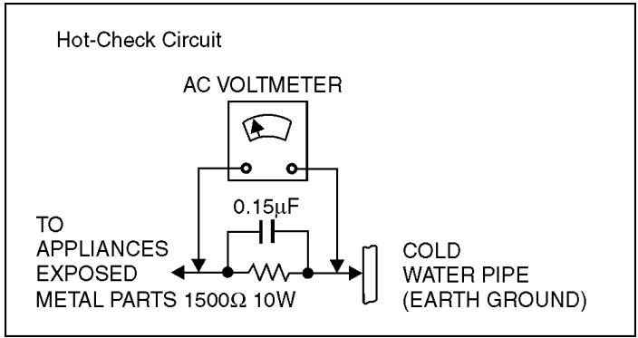
Figure 1
1.1.2. LEAKAGE CURRENT HOT CHECK
- Plug the AC cord directly into the AC outlet. Do not use an isolation transformer for this check.
- Connect a 1.5kΩ, 10 watts resistor, in parallel with a 0.15μF capacitor, between each exposed metallic part on the set and a good earth ground such as a water pipe, as shown in Figure 1.
- Use an AC voltmeter, with 1000 ohms/volt or more sensitivity, to measure the potential across the resistor.
- Check each exposed metallic part, and measure the voltage at each point.
- Reverse the AC plug in the AC outlet and repeat each of the above measurements.
- The potential at any point should not exceed 0.75 volts RMS. A leakage current tester (Simpson Model 229 or equivalent) may be used to make the hot checks, leakage current must not exceed 1/2 milliampere. In case a measurement is outside of the limits specified, there is a possibility of a shock hazard, and the equipment should be repaired and rechecked before it is returned to the customer.
2 WARNING
2.1. PREVENTION OF ELECTROSTATIC DISCHARGE (ESD) TO ELECTROSTATIC SENSITIVE (ES) DEVICES
Some semiconductor (solid state) devices can be damaged easily by static electricity. Such components commonly are called Electrostatic Sensitive (ES) Devices. Examples of typical ES devices are integrated circuits and some field-effect transistor-sand semiconductor "chip" components. The following techniques should be used to help reduce the incidence of component damage caused by electrostatic discharge (ESD).
- Immediately before handling any semiconductor component or semiconductor-equipped assembly, drain off any ESD on your body by touching a known earth ground. Alternatively, obtain and wear a commercially available discharging ESD wrist strap, which should be removed for potential shock reasons prior to applying power to the unit under test.
- After removing an electrical assembly equipped with ES devices, place the assembly on a conductive surface such as aluminum foil, to prevent electrostatic charge buildup or exposure of the assembly.
- Use only a grounded-tip soldering iron to solder or unsolder ES devices.
- Use only an anti-static solder removal device. Some solder removal devices not classified as "anti-static (ESD
protected)" can generate electrical charge sufficient to damage ES devices.
- Do not use freon-propelled chemicals. These can generate electrical charges sufficient to damage ES devices.
- Do not remove a replacement ES device from its protective package until immediately before you are ready to install it. (Most replacement ES devices are packaged with leads electrically shorted together by conductive foam, aluminum foil or comparable conductive material).
- Immediately before removing the protective material from the leads of a replacement ES device, touch the protective material to the chassis or circuit assembly into which the device will be installed.
Caution
Be sure no power is applied to the chassis or circuit, and observe all other safety precautions.
- Minimize bodily motions when handling unpackaged replacement ES devices. (Otherwise harmless motion such as the brushing together of your clothes fabric or the lifting of your foot from a carpeted floor can generate static electricity sufficient to damage an ES device).
IMPORTANT SAFETY NOTICE
There are special components used in this equipment which are important for safety. These parts are marked by ⚠️ in the schematic diagrams, Exploded Views and replacement parts list. It is essential that these critical parts should be replaced with manufacturer's specified parts to prevent shock, fire, or other hazards. Do not modify the original design without permission of manufacturer.
2.2. PRECAUTION OF LASER DIODE
CAUTION:
This product utilizes a laser diode with the unit turned “on”, invisible laser radiation is emitted from the pickup lens.
Wave length: 662 nm (DVDs)/780 nm (CDs)
Maximum output radiation power from pickup: 100μ W/VDE.
Laser radiation from the pickup lens is safety level, but be sure the followings:
- Do not disassemble the optical pickup unit, since radiation from exposed laser diode is dangerous.
- Do not adjust the variable resistor on the pickup unit. It was already adjusted.
- Do not look at the focus lens using optical instruments.
- Recommend not to look at pickup lens for a long time.
ACHTUNG:
THIS PRODUCT UTILIZES A LASER.
USE OF CONTROLS OR ADJUSTMENTS OR PERFORMANCE OF PROCEDURES OTHER THAN THOSE SPECIFIED HEREIN MAY RESULT IN HAZARDOUS RADIATION EXPOSURE.
2.3. SERVICE CAUTION BASED ON LEGAL RESTRICTIONS
General description about Lead Free Solder (PbF)
- The lead free solder has been used in the mounting process of all electrical components on the printed circuit boards used for this equipment in considering the globally environmental conservation.
- The normal solder is the alloy of tin (Sn) and lead (Pb). On the other hand, the lead free solder is the alloy mainly consists of tin (Sn), silver (Ag) and Copper (Cu), and the melting point of the lead free solder is higher approx.30 degrees C (86°F) more than that of the normal solder.
Service caution for repair work using Lead Free Solder (PbF)
- The lead free solder has to be used when repairing the equipment for which the lead free solder is used.
- To put lead free solder, it should be well molten and mixed with the original lead free solder.
- Remove the remaining lead free solder on the PCB cleanly for soldering of the new IC.
- Since the melting point of the lead free solder is higher than that of the normal lead solder, it takes the longer time to melt the lead free solder.
- Use the soldering iron (more than 70W) equipped with the temperature control after setting the temperature at 350 ± 30 degrees C ( 662 ± 86° F ). When soldering or unsoldering, please completely remove all of the solder on the pins or solder area and be sure to heat the soldering points with the Pb free solder until it melts enough.
Definition of PCB Lead Free Solder being used
- The letter of "Pbf is printed either foil side or component side using the lead free solder.
PbF
Recommended Lead Free Solder (Service Parts Route.)
- The following 3 types of lead free solder are available through the service parts route. RFKZ03D01K----(0.3mm 100g Reel) RFKZ06D01K----(0.6mm 100g Reel) RFKZ10D01K----(1.0mm 100g Reel)
Note
- Ingredient: tin (Sn), 96.5%, silver (Ag) 3.0%, Copper (Cu) 0.5%, Cobalt (Co) / Germanium (Ge) 0.1 to 0.3%
3 SERVICE NAVIGATION
3.1. SERVICE INFORMATION
This service manual contains technical information that will allow service personnel to understand and service this model.
Please place orders using the parts list and not the drawing reference numbers.
If the circuit is changed or modified, this information will be followed by a supplement service manual to be filed with the original service manual.
- This service manual does not contain the following information, because of the impossibility of servicing at component level.
- Schematic Diagram, Block Diagram and P.C.B. layout of RAM/Digital P.C.B. Module and Back End P.C.B. Unit.
- Parts List for individual parts of RAM/Digital P.C.B. Module.
- Exploded View and Parts List for individual parts of RAM/Digital P.C.B. Module.
- The following categories are recycle module parts. Please send them to the Central Repair Center.
• RAM/Digital P.C.B. Module: RFKNEX75EG • RAM/Digital P.C.B. Module: RFKNEX75EC • RAM/Digital P.C.B. Module: RFKNEX75EB • RAM/Digital P.C.B. Module: RFKNEX85EG • RAM/Digital P.C.B. Module: RFKNEX85EB - Back End P.C.B. Unit: REPD00311A (EX75EG/EX85EG) - Back End P.C.B. Unit: REPD00311C (EX75EB/EX85EB) - Back End P.C.B. Unit: REPD00311D (EX75EC)
3.2. CAUTION FOR DivX
Please always provide the information “Warning for Customers who use the DivX Video-on-Demand content.” to the customer together with the product, if you have to exchange the EEPROM, the P.C.B. including the EEPROM, or the product itself.
Also attach this information to every service part (EEPROM or P.C.B. including EEPROM).
This complete information is needed for every customer who is using the DivX Video-on-Demand Service.
Appendix:
* Parts that memorize user's information are only on the EEPROM. * The registration of the Registration Code is possible for half a year, up to 6 recorders, and up to 10 recorders a year. Every replacement of the EEPROM or the P.C.B. including the EEPROM spends one of these.
- The Registration Code is memorized in the EEPROM (RFKFxxxxxxx).
- If the Power & Digital I/F P.C.B. or the EEPROM is changed, a new Registration Code different from the previous one will be generated.
- In this case, the customer who is using the DivX Video-on-Demand service can no longer play any content that was or is purchased under that old registration code.
- Therefore, the customer will need to register a new registration code.
*Copy this page and cut on the dotted line and give the lower half to your customer.
Warning for Customers who use the DivX Video-on-Demand content.
- The registration code has been changed for the repair of the product or the product exchange.
- Obtain and register a new registration code, otherwise you will no longer be able to play DivX Video-on-Demand content.
- Follow the procedure on the DivX Video-on-Demand web site to register at http://vod.divx.com/
* If you do not use the DivX Video-on-Demand content, please ignore this warning.
4 SPECIFICATION
| Power supply: | AC220-240 V, 50/60 Hz | SD Card Slot: | JPEG (Still Picture DCF Standard) |
| Power consumption: | 33 W ±1,3 W | TIFF (uncompressed) | |
| Power save mode 2 W ±0,4 W | MPEG2 (rec. by Panasonic cam) | ||
| Dimensions and Mass: | 430 (W) x 329 (D) x 58 (H) mm(excluding protrusions) / 4.3 kg | Campable Cards: | SD Card, Multimedia CardminiSDTM Card (with adapter) |
| Operating temperature range: | +5 to +40 °C | Card format: | FAT12, FAT16 |
| Operating humility range: | 10 to 80 % RH (no condensation) | Card picture pixels: | 34x34 to 6144x4096 |
| Pickup Laser power: | CLASS1 | ||
| Pickup Wave length: | DVD 662 nm / CD 780 nmNo hazardous radiation is emitted with the safety protection | Video input AV1 / AV2: | 21 pin connector (1.0 Vp-p 75 Ω) |
| Video input AV3 / AV4: | pin jack connector (1.0 Vp-p 75 Ω) | ||
| S-Video input AV1 / AV2: | 21 pin connector(Y: 1.0 Vp-p, C: 0.3 Vp-p 75 Ω) | ||
| (NORSK) B∅LGELENGDE: | DVD 662 nm / CD 780 nm | ||
| Laserstyrke | Ingen farling stråling sendes ut | S-Video input AV3 / AV4: | pin jack connector(Y: 1.0 Vp-p, C: 0.3 Vp-p 75 Ω) |
| Recording system: | MPEG2 (Hybrid VBR)Audio: Dolby Digital 2CH | RGB Video input AV3 (PAL):DV input: | 21 pin connector (0.7 Vp-p 75 Ω)IEEE 1394 Standard 4 pin |
| Signal system: | PAL 625/50, NTSC 525/60 | ||
| DVD Region number: | Region No. 2 | Video output AV1 / AV2:FBAS Video output (composit): | 21 pin connector (1.0 Vp-p 75 Ω)pin jack connector (1.0 Vp-p 75 Ω) |
| Internal Hard Disc Drive: | 160 GB (EX75) / 250 GB (EX85) | S-Video output AV1: | 21 pin connector (1.0 Vp-p 75 Ω) |
| DVD Recording / Playable discs: | DVD-RAM (12 cm 4.7 GB)DVD-RAM (12 cm 9.4 GB)DVD-RAM (8 cm 2.8 GB)DVD-R (12 cm 4.7 GB)DVD-R (8 cm 1.4 GB)DVD-RW (12 cm 4.7GB)DVD+R (12 cm 4.7 GB)DVD+RW (12 cm 4.7 GB) | S-Video output (cinch):S-Video output:RGB Video output AV1:Component Video output: | pin jack connector (1.0 Vp-p 75 Ω)S connector (1.0 Vp-p 75 Ω)21 pin connector (0.7 Vp-p 75 Ω)Y pin jack (1.0 Vp-p 75 Ω)PB pin jack (0.7 Vp-p 75 Ω)PR pin jack (0.7 Vp-p 75 Ω)Version 1.2a (EDID Vers. 1.3) |
| DVD approximate Recording time: | XP: 10 MBps (60 min)SP: 5 MBps (120 min)LP: 3 MBps (240 min)EP: 1.7 / 1.2 MBps (360 - 480 min) | HDMI output (19 pin type A): | 21 pin connector (-6 dBV 500 mV)pin jack (-6 dBV 500 mV)pin jack (-6 dBV 500 mV)PCM, Dolby Digital, DTS, MPEG |
| Additional playable discs: | DVD-RAM (VR format)DVD-RW (VR format)DVD-R(MP3, DivX (Except EB), JPG)DVD-R DL, DVD+R DLDVD-Video, DVD-AudioCD-Audio (CD-DA), Video CDSVCD (IEC62107)CD-R, CD-RW(CD-DA, MP3, DivX (Except EB),JPG, VCD) | Audio input AV1 / AV2:Audio input AV3 / AV4:Audio output (cinch):Optical output: | 21 pin connector (-6 dBV 500 mV)pin jack (-6 dBV 500 mV)PCM, Dolby Digital, DTS, MPEG |
| TV tuner system EG/EC-Model | PAL-BGH, SECAM-BG | ||
| TV tuner channel EG/EC-Model: | VHF: E2-E12UHF: CH21-CH69CATV: S01-S05 (S1-S3)CATV: S1-S20 (M1-U10)CATV: S21-S41 | ||
| TV digital tuner (DVB-T) EG/EC | VHF: CH5-CH12UHF: CH21-CH69 | ||
| TV tuner system EB-Model | PAL-I | ||
| TV tuner channel EB-Model: | UHF: CH21-CH68 | ||
| TV digital tuner (DVB-T) EB-Model | UHF: CH21-CH68 | ||
| Active Antenna EG/EC-Model: | 5V switched 50mA max. | ||
| Active Antenna EB-Model: | not provided | ||
| RF Converter Output: | not provided |
5 NEW FEATURE
5.1. ABOUT DivX (EXCEPT EB)
5.1.1. GENERAL
DivX is a new video compressing format that is applied
MPEG-4 technology to improve quality and the compressibility and it is developed by the DivXNetworks, Inc., Video file of high resolution and the high picture quality can be made thought it is a high compressibility.
DivX codec is necessary for converting video to DivX file and playback files made.
5.1.2. OPERATING INSTRUCTIONS ABOUT DivX VIDEO-ON-DEMAND CONTENT
DivX Video-on-Demand (VOD) content is encrypted for copyright protection. In order to play DivX VOD content on this unit, you first need to register the unit.
Follow the online instructions for purchasing DivX VOD content to enter unit's registration code and register unit. Visit www.divx.com/vod for mor information.
Display unit's registration code: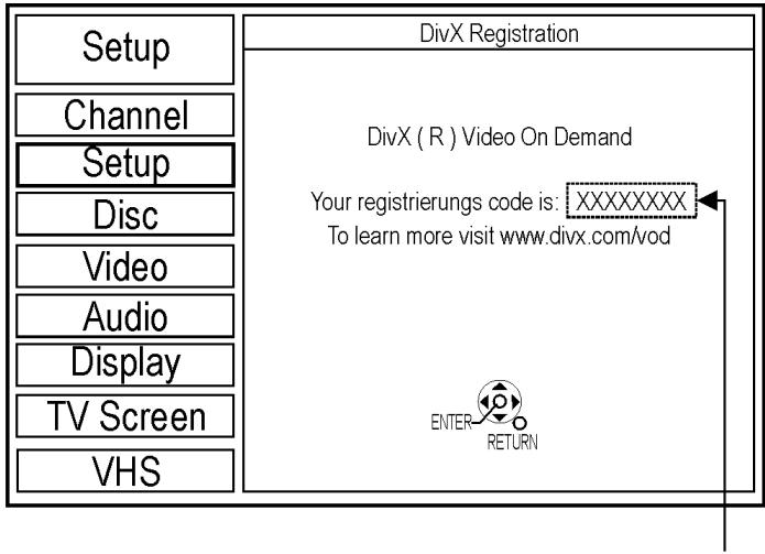
8 alphanumeric characters
- We recommend that you make a note of this code for future reference.
- After playing DivX VOD content for the first time, another registration code is then displayed in "DivX Registration". Do not use this registration code to purchase DivX VOD content. If you use this code to purchase DivX VOD content and play the content on this unit, you will no longer be able to play any content that you purchased using the previous code.
- If you purchase DivX VOD content using a registration code different from this unit's code, you will not be able to play this content. ("Authorization Error" is displayed.)
Some DivX VOD content can only be played a set number of times.
When you play this content, the remaining number of plays is displayed. You cannot play this content when the number of remaining plays is zero. ("Rental Expired" is displayed.)
When playing this content
• The number of remaining plays is reduced by one if you press [POWER], [STOP], [backwards SKIP], [backwards SLOW / SEARCH], or [forwards SLOW / SEARCH], etc., and arrive at another content or the start of the content being played. – Scheduled [DRIVE SELECT] to change drive
* Resume functions do not work.
Typical Playback procedure of DivX VOD (Video On Demand):
| Case 1 | When DivX VOD is used newly. |
| Case 2 | When EEPROM or P.C.B. includin EEPROM was replaced for repairing. |
| Case 3 | When recorder was exchanged to another recorder for repairing. |
| Case 4 | When customer own second recorder. |
| Case 5 | When owner of recorder was changed to another. |
CASE 1 WHEN DivX IS USED NEWLY
Registration Code display (code is an example)
![graph TD A["Server"] --> B["Mr. A"] B --> C["DivX(R) Video On Demand\nYour registration code is : AAAA-AAAA\nTo learn more visit www.divx.com/vod\n[Done"]]](/content/2019/11/105906/images/b1d019171880bd1ca8a8ab2cab095c167a400ea3b35049599acaa6238ee729db.jpg)
Case 1
Activation: File obtaining (code/ID are examples)
![graph TD A["Mr. A"] --> B["File G (Encryption)"] C["Internet"] --> B B --> D["<Input items> RegistratinCode: AAAA-AAAA<br>UserId: user 1"]](/content/2019/11/105906/images/a08150eb0127902e0239135c3e7f0f2c0e187ae11a4828c3601f15aa2396437d.jpg)
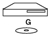
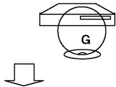
Activation: File Playback
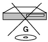
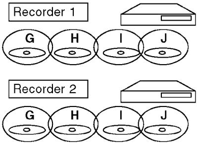
Activation cannot be done for other recorders by file G.
Recorder is set for user 1
→ File G can be played back
Registration Code display (code is an example)
![DivX(R) Video Your registration code is: BBBB-BBBB To learn more visit www.divx.com/vod [Done]](/content/2019/11/105906/images/9088037c9930a43243d09a2b1387e9bb5ea78fd17c72a409a3a52e8fd74f1bbf.jpg)
*The code different from code before Activation is displayed.
(This code is unnecessary for Mr. A)

Obtainment/Playback of additional file after Activation (code/ID is an example)
![graph TD A["Mr. A"] --> B["UserId: user 1"] B --> C["Computer"] D["H"] -->|File Y (Encryption)| C](/content/2019/11/105906/images/8136f49447a6f1aadee5c9131ea2edc334efdcb679bae8aee25aae19ce980280.jpg)
File of user 1 can be played back
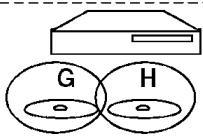
| CASE 2 | WHEN EEPROM OR P.C.B. INCLUDING EEPROM WAS REPLACED FOR REPAIRING |
| CASE 3 | WHEN RECORDER WAS EXCHANGED TO ANOTHER RECORDER FOR REPAIRING |
New Registration Code is displayed (code is an example)
![graph TD A["Mr. A"] --> B["DivX(R) Video On Demand"] B --> C["Your registration code is : CCCC -CCCC"] C --> D["To learn more visit www.divx.com/vod [Done"]] D --> E["Down Arrow"]](/content/2019/11/105906/images/c5157a980e45d0a70471a0e1442569c3c1f6daf5d562a170b77e61c7500373d6.jpg)
Case 2
Activation: File obtaining (code/ID are example)
![graph TD A["Mr. A"] --> B["File I (Encryption)"] B --> C["Internet"] D["<Input items> Registration Code: CCCC-CCCC\nUserId: user 1"] --> B B --> E["Down arrow"]](/content/2019/11/105906/images/fd0695053be226f1c31e183d5ec1aec75ebac0a9400ff863f67f8c174ebda1c8.jpg)
Activation: File Playback
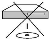
Activation cannot be done for other recorders by file I.
Recorder is set for user 1
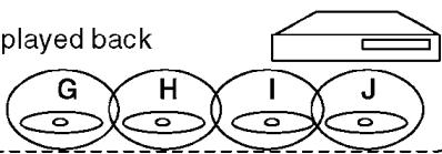
→ File G, H, I can be played back
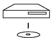

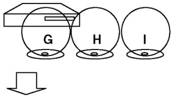
Registration Code display after Activation (example)
![DivX(R) Video On Demand Your registration code is: DDDD-DDDD To learn more visit www.divx.com/vod [Done]](/content/2019/11/105906/images/80f29dbeaa22ae884bab59f973579107ae3311adc4ade61e93505455ffff02a5.jpg)
The code different from code before Activation is displayed.
(This code is unnecessary for Mr. A)

Obtainment/Playback of additional file after Activation (code/ID is an example)
![graph TD A["Mr. A"] --> B["File J (Encryption)"] C["J"] --> B B --> D["UserId: User 1"]](/content/2019/11/105906/images/fffeafd27cd5d30dd431f438828d1208c579530f448d7f2212fda84c6c0d871a.jpg)
Files of user 1 can be played back
Case 3
CASE 4 WHEN CUSTOMER OWNS SECOND RECORDER
Registration Code display of second recorder (code is an example)
![graph TD A["Mr. A"] --> B["DivX(R) Video On Demand"] B --> C["Your registration code is : EEEE-EEEE\nTo learn more visit www.divx.com/vod"]](/content/2019/11/105906/images/cfdb722bf000d51dab74388d7e5c576737664e509b44a2eb33bccbc54931e500.jpg)
Case 4
Activation: File obtaining (code/ID are example)
![graph TD A["Mr. A"] --> B["File I (Encryption)"] B --> C["Internet"] C --> D["<Input items> Registration Code: EEEE-EEEE<br>UserId: user 1"] D --> B](/content/2019/11/105906/images/f240170403b331962aa67b60fcb80b8fd6a1b92f19ed2dc5360ec3838b76a82b.jpg)
Activation: File Playback
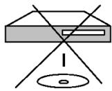
Activation cannot be done for other recorders by file I.
Recorder is set for user 2
→files G, H, I
Recorder 2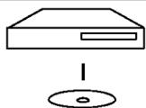


Registration Code display after Activation (example)
Recorder 2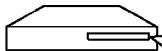
Divx(R) Video On Demand
Your registration code is : FFFF-FFFF
To learn more visit www.divx.com/vod
[Done]

Obtainment/Playback of additional file after Activation (code/ID is an example)
![graph TD A["Mr. A"] --> B["File J (Encryption)"] C["J"] --> B B --> D["UserId :User 1"]](/content/2019/11/105906/images/1df92576e4e16b54ecf89c3b1854d598deac1e99006f154b0831bbb0d060399a.jpg)
Files of user 1 can be played back
CASE 5 WHEN OWNER OF RECORDER WAS CHANGED TO ANOTHER![graph TD A["Friend"] --> B["Server"] B --> C["Mr. A"]](/content/2019/11/105906/images/068b3e13e9d83da441b3b091015a73cfaf7191ef87dababe1aff9d8fa52627bd.jpg)
New user
Mr. B (user 2)
It is necessary to update information on the recorder
Case 5
Activation
Registration Code is displayed![DivX(R) Video On Demand Your registration code is: IJKL-MNOP To learn more visit www.divx.com/vod [Done]](/content/2019/11/105906/images/7bf27c4fc0c2ab52e8cabc3c3a678cf07a2574eb522b02236c2ef0bab5eb07b1.jpg)
Activation: File obtaining (code/ID are example)
![graph TD A["Mr. B"] --> B["File K (Encryption)"] C["K"] --> B B --> D["Internet"] E["<Input items> <br> • RegistratinCode: IJKL-MNOP <br> • UserId: user 2"] --> D](/content/2019/11/105906/images/00aa4ab72f774e82821b6b8759214bb8f7a879d7bc09198f90e35969edca8eed.jpg)
Activation: File Playback
Recorder is set for user 2
→ Only file K can be played back
Only files of user 2 can be played back


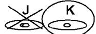
* File G is an Activation file too, but Activation is not done because the code when obtaining it is different.
FILE KIND
(There are two kinds of Activation files as follows too.)
- Rental: There is a playback limitation • Purchase: Unrestricted
Also there is next file as DRM files besides the above-mentioned.
- Base:
It is not necessary to approve though the contents is being encoded.
If it is recorder/player for DRM, any can play back. (It is the same as usual DivX file when seeing from user.)
SCREEN SHIFT (Error display)
Whether approval is OK or not.
Whether the recorder corresponds to the user information on the file or not.
![graph TD A["Purchase file"] --> B{Approval error} B --> C["Authorization Error"] C --> D["View DivX(R) VOD Rental"] D --> E{There are rental remainders.} E --> F["Rental invalidity"] F --> G["Rental Expired"] G --> H["Playback starts"] C --> I["Approval is OK"] D --> J["Approval is OK"] K["Playback…](/content/2019/11/105906/images/b7e69064da8c337320668b1ad229e2fd678977e499cb0cdc10e91ec6ffa5495c.jpg)
5.1.3. ABOUT DivX DRM
DivX files include files to which DRM (Digital Rights Management) is applied and files to which it is not applied. This item is content that relates only to the handling of files to which DRM is applied.
- Registration Code display function
- User's registration and approval function
- Rental management function
5.1.3.1. REGISTRATION CODE DISPLAY FUNCTION
The Registration Code is an alphanumeric character sequence of 8 bytes input as recorder information when a user purchases or rents a DivX DRM file over a network. The registration code is a randomly generated character sequence and differs for each recorder. Moreover, the registration code is updated by new user authentication even on the same recorder.
5.1.3.2. USER'S REGISTRATION AND APPROVAL FUNCTION
- Only one user can register for one recorder. If user registration is not done with the recorder, DivX files cannot be played back.
- User registration is performed only when a DivX DRM file is first chosen by the recorder.
- DivX DRM files that can perform user registration are only files that are registered with a Registration Code and purchased or rented.
- User authentication is performed whenever a DivX DRM file is played back. An error message is displayed when user registration and approval fail.
5.1.3.3. RENTAL MANAGEMENT FUNCTION
There are purchase files without a limit on the number of playbacks and rental files with a limit on the number of playbacks as DivX files. The number of playbacks of a rental file is counted by the recorder. When a rental file is played, the remaining number of times that can be played back will be shown to users, and the recorder requests users to input yes or no. The following specifications have been installed for the rental files in order to clarify the counting condition of the number of times of playback.
- Conditions for counting the number of times a file is played.
- When a file was opened successfully. (At the time of playback start)
- When you have performed a review operation from the start. (Skip to file head)
- At this time, the remaining number of times that can be played back and a confirmation message
[Do you really want to play?] are displayed.
- When the playback point has been skipped to the top of the title, the number of plays is not counted if the top of the title was not recognized.
- Even if a power failure occurs after the start of playback of a rental file, the number of times played counted at the start of playback is retained as is.
(Though playback stops due to power failure,
the number of times played is not counted.)
When it has reached the head of the title, playback ends, and the screen becomes the DivX menu (there is no resume), and then the cursor is located on the title that has been played back. Then, if the same file is continuously played back, it begins playback from the file head.
Note:
The above-mentioned stored user information and number of times played are not erased by firmware updates or by initialization via test mode.
5.2. HDAVI CONTROL (HDMI LINK)
Linked operations by HDAVI Control (HDMI Link)
5.2.1. WHAT IS HDMI
HDMI is an abbreviation for [High-Definition Multimedia Interface], and it is a digital interface standard for next-generation TVs, corresponding to the following features.
- Non-compressing high-quality digital image.
- Digital transmission of multi-channel digital audio.
- Two-way communication of control signals for controlling and coordinating between equipment.
| Cable | Transmission method | Directionality | Transmission signal | Feature |
| HDMI Cable | Digital (~4.455Gbps) | One-way | Digital image (none-compression high-definition television image) | Clock line in one system and data line in three systems can high-speed communicate high reliability because of balance communication that uses three respectively every one system.Moreover, because high-speed data line in three system can be used at same time, it has ten of other digital cables times or more transmission ability.And can transmit high-definition television image of non-compression, 24 bit high sound quality PCM voice of multi-CH of DVD audio (to 6ch) and Bit stream signal of surround to 8ch of DVD video (5.1ch, 6.1ch, and 7.1ch, etc.) as a digital signal of no deterioration.It has power supply line and a interactive control signal line communication independent of AV signal, a Cd can an advanced control between equipments. Therefore it can correspond to making of AV equipment in the future highly a network. |
| One-way | Digital Audio (6ch/24 bit high sound quality PCM of DVD audio/Bit stream of surround to 8ch of DVD video) | |||
| Interactive | Digital control signal (Advanced control between equipments) |
Pin Name
| 1 | TMDS Data2(+) | 11 | TMDS Clock(shield) |
| 2 | TMDS Data2(shield) | 12 | TMDS Clock(-) |
| 3 | TMDS Data1(-) | 13 | CEC (Linked operation control) |
| 4 | TMDS Data1(+) | 14 | NC |
| 5 | TMDS Data1(shield) | 15 | SCL |
| 6 | TMDS Data2(-) | 16 | SDA |
| 7 | TMDS Data0(+) | 17 | Ground |
| 8 | TMDS Data0(shield) | 18 | +5v Power |
| 9 | TMDS Data0(-) | 19 | Hot Plug Detect |
| 10 | TMDS Clock(+) |
Pin layout of the HDMI cable plug, as seen from the outside.
| 1 | 3 | 5 | 7 | 9 | 11 | 13 | 15 | 17 | 19 | ||
| 2 | 4 | 6 | 8 | 10 | 12 | 14 | 16 | 18 | Shell |
5.2.2. LINK FUNCTIONS
| Functions |
| (1) Automatic Input switch |
| (2) Link of Power |
5.2.3. OUTLINE OF EQUIPMENT LINKED FUNCTIONS
1. Automatic Input Switch
When playback or GUI (Graphical User Interface) display is started by DIGA, it turns on the power of VIErA and displays the picture from DIGA on the VIErA screen.
a. Starting of playback:
This includes automatic playback of DVD-Video and so on. It also includes the picture of the screen saver.
b. GUI display:
FUNCTIONS, DIRECT NAVIGATOR, TV PROGRAM, PROG/CHECK, Timer Recording, G-code, Initial setting, Playback setting, Play list, SD/DVD guide, Warning messages that the user can select, and so on.
![graph TD A["Input Selection"] --> B["DIGA Remote Controller"] B --> C["Playback"] C --> D["Playback"] D --> E["Stop"] style A fill:#f9f,stroke:#333 style B fill:#ccf,stroke:#333 style C fill:#cfc,stroke:#333 style D fill:#fcc,stroke:#333 style E fill:#ffc,stroke:#333](/content/2019/11/105906/images/901eba1698ccf302fbadd5288b9d5a3ab9a0667e6cac38af4a6591898f461e51.jpg)
2. Power Link
Power of DIGA is turned off linking to POWER OFF of VIErA.
- Power not turned on linking to POWER ON of VIErA.
- It is limited in following cases that DIGA links to POWER OFF of VIErA.
- During EE display (While Timer recording is being executed/Functions is being displayed are included.)
However except cases below.
- During EE display, but manual recording is being executing/during EXT_Link recording.
- During Tray is being opened.
- Case that DIGA is in status that power cannot turn off (during dubbing, during finalize).
![graph TD A["POWER button"] -->|P-OFF| B["P-ON"] B -->|P-OFF| C["P-ON → P-OFF"] D["VIErA Remote Controller"] -->|P-OFF| E["P-ON"]](/content/2019/11/105906/images/4f98e9d8bfd61a9bfd6e2895becc46f9fda220d6f312752f5bb385b3f18636cc.jpg)
6 LOCATION OF CONTROLS AND COMPONENTS
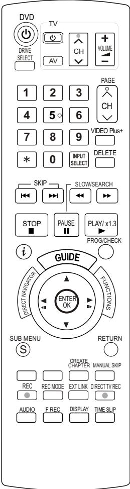
Remote Control
DVD

Stand-by/on switch
Press to switch the unit from on to stand-by mode
or vice versa. In stand-by mode, the unit is still consuming a small amount of power.
Switching this unit into standby mode does not disconnect it from the mains.

Select the HDD, DVD or SD drive.

Direction buttons in the menu guide. Select groups or titles.
ENTER: Select or save a setting.
◀ Still picture or slow motion playback.

Display the programme information from the TV GUIDE or the Banner.

Check / Change a Timer recording.

Launch sub menus.

Return to the previous menu.

VIDEO Plus+ menu (EB-model) or ShowView menu (EG/EC-models) for analogue stations

Search or slow motion playback.

Stops recording, replay or forward / reverse action

Pause a recording or playback.

Start the recording.

Record mode button XP, SP, LP, EP

Record with external recording control.

Direct TV recording.

Selecting audio channel / soundtrack.

Flexible recording.

Show on screen menu.

Turn the television set on and off.

Select the AV input on the television set.

CH: Select the channel on the television set. VOLUME: Volume control of the television set.

CH: Select the channel on the Recorder. PAGE: Scroll in the electronic TV Guide.
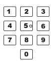
Number buttons - direct input
VCD 5:05 15:15
JPEG MP3 5: 0 0 5° 15: 0 1 5°
JPEG 5: 0 0 0 5° 15: 0 0 1 5°

GUIDE: Launch the TV Guide menu.

DIRECT NAVIGATOR: title view TOP MENU: Main menu of DVD-video.

FUNCTION selection menu.

Cancel a function.

Switch the AV input between AV1, AV2, AV3 (front), AV4, and DV IN.

Delete items.

Start playback.
RAM - You can increase the playback speed by holding PLAY during playback.

Skip chapters, titles, or pictures.

Menu guide (red button): Profile, Guide, Digital Text, Manual Tuning

Menu guide (green button): Profile, Guide, Digital Text

Menu guide (yellow button): Profile, Guide, Digital Text. CREATE CHAPTER: Dividing a recording into chapters.

Menu guide (blue button): Profile, Guide, Digital Text. MANUAL SKIP: Jump forward 30 seconds.

Select the time frame.
7 OPERATING INSTRUCTIONS
7.1. TAKING OUT THE DISC FROM DVD-DRIVE UNIT WHEN THE DISC CANNOT BE EJECTED BY OPEN/CLOSE BUTTON
7.1.1. FORCIBLE DISC EJECT
7.1.1.1. WHEN THE POWER CAN BE TURNED OFF
- Turn off the power and press [STOP] and [CH UP] keys on the front panel simultaneously for 5 seconds.
7.1.1.2. WHEN THE POWER CANNOT BE TURNED OFF
- Press [POWER] key on the front panel for over 10 seconds to turn off the power forcibly, then press [STOP] and [CH UP] keys on the front panel simultaneously for 5 seconds.
7.1.2. WHEN THE FORCIBLE DISC EJECT CANNOT BE DONE
- Turn off the power and pull out the AC cord.
- Remove the Top Case.
- Place the deck so that the bottom can be seen.
- Push the SLIDE CAM with the Eject Pin (JZS0484) or a small flat-head screwdriver in the direction of the arrow to eject the tray slightly.
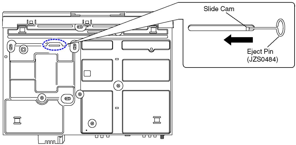
- Place the deck upward and push out the Tray with the Eject Pin (JZS0484) or a small flat-head screwdriver.

8 SERVICE MODE
8.1. SELF-DIAGNOSIS AND SPECIAL MODE SETTING
8.1.1. SELF-DIAGNOSIS FUNCTIONS
The Self-Diagnosis Function provides error information to service personnel via the “Self-Diagnosis Display” when any error has occurred.
U**, H** and F** are stored in memory and held.
You can check the latest error code by transmitting [0] [1] of the Remote Controller in Service Mode.
Automatic Display on FL will be cancelled when the power is turned off or AC input is turned off during self-diagnosis display is ON.
| Error Code | Diagnosis contents | Description | Monitor Display | Automatic FL display |
| IR ERR | IR communication error | [IR ERR] is displayed when communication between Timer microprocessor and IR microprocessor fails. | No display | IR ERR |
| No REC | Recording is impossible | [No REC] is displayed when recording is impossible due to the defect, dirt or wound of media. | No display | NOREC |
| U30 | Remote control code error | Display appears when main unit and remote controller codes are not matched. | No display | DVD * |
| ** is remote controller code of the main unit. Display for 5 seconds. | ||||
| U59 | Abnormal inner temperature detected | Display appears when the drive temperature exceeds 70°C.The power is turned off forcibly.For 30 minutes after this, all key entries are disabled. (Fan motor operates at the highest speed for the first 5 minutes. For the remaining 25 minutes, fan motor is also stopped.) The event is saved in memory as well. | No display | U59 |
| “U59 is displayed for 30 minutes. | ||||
| U61 | The unit is carrying out its recovery process (with no disc in the disc tray). | * The unit detected an error while recording or playing with with no disc in the disc tray.The unit is carrying out its recovery process.This process restores the unit to normal operation. The unit is not broken. Wait until the message disappears. | No display | U61 |
| U80 | ST Microprocessor Communication Error on Timer Bus | Displayed appears when ST Microprocessor Communication Error on Timer Bus occurs. | No display | U80 |
| “U80” is displayed till Power Key is pressed. | ||||
| U81 | ST Microprocessor Communication Error on UART | Displayed appears when ST Microprocessor Communication Error on UART occurs. | No display | U81 |
| “U81” is displayed till Power Key is pressed. | ||||
| U88 | The unit is carrying out its recovery process (with no disc in the disc tray). | * The unit detected an error while recording or playing with with no disc in the disc tray.The unit is carrying out its recovery process.This process restores the unit to normal operation. The unit is not broken. Wait until the message disappears. | No display | U88 |
| U99 | Hang-up | Displayed when communication error has occurred between Main microprocessor and Timer microprocessor. | No display | U99 |
| Displayed is left until the [POWER] key is pressed. | ||||
| H19 | Inoperative fan motor | When inoperative fan motor is detected after powered on, the power is turned off automatically.The event is saved in memory. | No display | No display |
| F00 | No error information | Initial setting for error code in memory(Error code Initialization is possible with error code initialization and main unit initialization.) | No display | No display |
| F58 | Drive hardware error | When drive unit error is detected, the event is saved in memory. | No display | No display |
| F34 | Initialization error when main microprocessor is started up for program recording | When initialization error is detected after starting up main microprocessor for program recording, the power is turned off automatically.The event is saved in memory. | No display | No display |
| UN-SUPPORT | Unsupported disc error | *An unsupported format disc was played, although the drive starts normally.*The data format is not supported, although the media type is supported.*Exceptionally in case of the disc is dirty. | "This disc is incompatible." | UNSUP↓PORTDisplay for 5 seconds. |
| NO READ | Disc read error | *A disc is flawed or dirty.*A poor quality failed to start.*The track information could not be read. | "Cannot read.Please check the disc." | NOREAD |
| HARD ERR | Drive error | The drive detected a hard error. | "DVD drive error." | Display for 5 seconds.HARD↓ERR |
| SELF CHECK | Restoration operation | Since the power cord fell out during a power failure or operation, it is under restoration operation.*It will OK, if a display disappears automatically. If a display does not disappear, there is the possibility that defective Digital P.C.B. / RAM drive. | No display | SELF↓CHECK |
| PLEASE WAIT | Unit is in termination process | Unit is in termination process now.“BYE” is displayed and power will be turned off.In case “Quick Start” of setup menu is ON, it is displayed in restoration operation for AC off. | No display | PLEASE↓WAIT |
| UN-FORMAT | Unformatted disc error | You have inserted an unformatted DVD-RAM or DVD-RW that is unformatted or recorded on other equipment. | Format:This disc is not formatted properly.Format the disc in DISK MANAGEMENT? | UNFOR↓MAT |
DMR-EX75EG / DMR-EX75EC / DMR-EX75EB / DMR-EX85EG / DMR-EX85EB
| Error Code | Diagnosis contents | Description | Monitor Display | Automatic FL display |
| HDD ERR | [HDD ERR] is displayed when start up of HDD was failed.(Except error of setting of Power on Stand-by) | 1. When normal start up was failed2. When start up at HDD boot was failed3. When start up from state of P-OFF was failed4. When start up from state of HDD SLEEP was failed.[HDDERR] is displayed when above each start up of HDD was failed.* In case 1.), tray opens automatically and [HDDERR] is displayed until version up disc is inserted. | No display | HDDERR |
| HDD NG | Power on Stand-by setting error | [HDD NG] is displayed when power on Stand-by setting of HDD is NG or when HDD which power on Stand-by is not set to is used.Please try to replace HDD with junine HDD as service parts. | No display | HDD NG |
8.1.2. SPECIAL MODES SETTING
| Item | FL display | Key operation | |
| Mode name | Description | Front Key | |
| TEST Mode | *All the main unit's parameters (include tuner) are initialized. | TM AV1 | Press [STOP], [CH UP] and [OPEN/CLOSE] keys simultaneously for five seconds when power is off. |
| Rating password | The audiovisual level setting password is initialized to "Level 8". | INIT | Open the tray, and press [REC] and [PLAY] simultaneously for 5 seconds. |
| Service Mode | Setting every kind of modes for servicing.*Details are described in "Service Mode". | SERV | When the power is off, press [CH UP], [OPEN/CLOSE] and [REC] keys simultaneously for 5 seconds. |
| Forced disc eject | Removing a disc that cannot be ejected.The tray will open and unit will shift to P-off mode.*When Timer REC is ON or EXT-LINK is ON, execute " Forced disc eject " after releasing Timer REC or EXT-LINK.*This command is not effective during "Child lock" is ON.While Demonstration Lock is being set, this Forced disc eject function is not accepted.If this command was executed while TIMER REC is being set, TIMER REC setting will be kept. | The display before execution leaves.***** | When the power is off, press [STOP] and [CH UP] keys simultaneously for 5 seconds. |
| Child lock/unlock | Set or release "Child Lock". | X HOLD | Press [ENTER] and [RETURN] by remote controller simultaneously until [X-HOLD] is displayed. |
| NTSC/PAL system select | To switch PAL/NTSC alternately. | The display before execution leaves.***** | While the power is on (E-E mode), press [STOP] and [OPEN/CLOSE] simultaneously for 5 seconds. |
| Forced power-off | When the power button is not effective while power is ON, turn off the power forcibly.*When Timer REC is ON or EXT-LINK is ON, execute "Forced Power-off" after releasing Timer REC or EXT-LINK. | Display in P-off mode. | Press [Power] key over than 10 seconds. |
| Item | FL display | Key operation | |
| Mode name | Description | Front Key | |
| Aging | Perform sequence of modes as * Aging Description shown below continually.Caution:All programs in DVD-RAM disc will be deleted because Formatting is done once in Aging process. | Display following the then mode. | When the power is ON, press [STOP], [POWER] and [OPEN/CLOSE] simultaneously for over 5 seconds and less than 10 seconds.NOTE1:If Unit has not turned into Aging mode by operations shown above, execute TEST MODE once and re-execute operation shown above. (*All the main unit's parameters include tuner are initialized by TEST mode.)NOTE2:If the unit has hung-up because of pressing keys for over 10 seconds, once turn off the power, and re-execute this command.*When releasing Aging mode, press [POWER] key. |
Aging Contents (Example):
![graph TD A["Format (DVD)"] -->|At start, and in the case that the memory remainder of HDD are 0| B["Format (HDD)"] A -->|If the memory remainder of DVD only are 0| C["REC & PLAY (HDD)"] C --> D["REC & PLAY (DVD)"] D --> E["REC (HDD) & PLAY (DVD) *1"] E --> F["REC (DVD) & PLAY (HDD) *2"] F --> G["REC…](/content/2019/11/105906/images/c3b1d54132376c77b05bb349792cdedf932552fc20e41c07696b6018f00c8ad5.jpg)
*1 : REC (HDD) & PLAY (DVD) content of operation
HDD→REC, DVD→PLAY, CUE, REV, PLAY, PAUSE, SLOW, R-SLOW, PLAY, PROGRAM NAVI
*2 : REC (DVD) & PLAY (HDD) content of operation
DVD→REC, HDD→PLAY, CUE, REV, PLAY, PAUSE, SLOW, R-SLOW, PLAY, PROGRAM NAVI, TRAY OPEN/CLOSE
*3 : REC & PLAY (HDD)→REC (HDD) & PLAY (DVD) content of operation
HDD→REC & PLAY, DVD→PLAY, TRAY OPEN/CLOSE
| Demonstration lock/unlock | Ejection of the disc is prohibited.The lock setting is effective until unlocking the tray and not released by “Main unit initialization” of service mode. | *When lock the tray. | When the power is on, press [STOP] and [POWER] keys simultaneously for 5 seconds. |
| LOCK | |||
| “LOCK” is displayed for 3 seconds. | |||
| *When unlock the tray. | When the power is on, press [STOP] and [POWER] keys simultaneously for 5 seconds. | ||
| UNLOCK | |||
| “UNLOCK” is displayed for 3 seconds. | |||
| *When press OPEN/CLOSE key while the tray being locked. | Press [OPEN/CLOSE] key while the tray being locked. | ||
| LOCK | |||
| Display “LOCK” for 3 seconds. | |||
| Item | FL display | Key operation | |
| Mode name | Description | Front Key | |
| ATP re-execution | Re-execute ATP. | Display at ATP executing. | When the power is on (E-E mode), press [CH UP] and [CH DOWN] simultaneously for 5 seconds. |
| Progressive initialization | The progressive setting is initialized to Interlace. | The display before execution leaves. | When the power is on (E-E mode), press [STOP] and [PLAY] simultaneously for 5 seconds. |
8.1.3. SERVICE MODES AT A GLANCE
Service mode setting: While the power is off, press [REC], [CH UP] and [OPEN/CLOSE] simultaneously for five seconds.
| Item | FL display | Key operation | |
| Mode name | Description | (Remote controller key) | |
| Release Items | Item of Service Mode executing is cancelled. | SERV | Press [0] [0] or [Return] in service mode. |
| Error Code Display | Last Error Code of U/H/F held by Timer is displayed on FL.*Details are described in “Self-Diagnosis Functions”. | ♣□□*♣shows U/H/F□□shows numberIf any error history dose not exist, [F00] is displayed. | Press [0] [1] in service mode |
| ROM Version Display | 1. Region code (displayed for 5 sec.)2. Main firm version (displayed for 5 sec.)3. Timer firm version (displayed for 5 sec.)4. Drive firm version (displayed for 5 sec.)5. ROM correction version (left displayed) | 1.NO **2.**********3.**********4.****5.***“” are version displays. | Press [0] [2] in service mode |
| White Picture Output | White picture is output as component Output from AV Decoder.*White picture (Saturation rate : 100%)*It is enable to switch Interlace/Progressive by “I/P switch: [1] [4]” | *Initial mode is “Interlace”.WHIT I | Press [1] [1] in service mode. |
| Switch Interlace/ProgressiveWHIT | Press [1] [4] in White Picture Output mode.*I/P are switched alternately. | ||
| Magenta Picture Output | Magenta picture is output with Component Output from AV Decoder.*Magenta picture(Saturation rate: 100%)*It is enable to switch Interlace/Progressive by “I/P switch: [1] [4]” | *Initial mode is “Interlace”.PAGE I | Press [1] [2] in service mode. |
| Switch Interlace/ProgressivePAGE | Press [1] [4] in Magenta Picture Output mode.*I/P are switched alternately. | ||
| RTSC Return in XP(A & V) | AV1 input signal is encoded (XP), decoded (XP) and output decoded signal to external without DISC recording and DISC playback. | Initial mode: EE2/ Interlace/ XP/Audio 48kHzEE2 | Press [1] [3] in service mode. |
| Switch Interlace/ProgressiveEE2P48 | Press [1] [4] in RTSC Return XP mode.*I/P are switched alternately. | ||
| Audio 44.1 kHz/ 48 kHz SwitchEE2P44 | Press [2] [4] in RTSC Return XP mode.*48 kHz / 44.1 kHz are switched alternately. | ||
| I/P Switch | Switch Interlace and Progressive in EE mode.*Initial setting is “Interlace”.*This command is effective during executing “White Picture Output”, “Magenta Picture Output” and “RTSC Return in XP (A & V)” modes. | Initial mode is InterlaceSERV PSwitch Interlace/ProgressiveSERV I | Press [1] [4] in I/P Switch mode.*I/P are switched alternately. |
| Audio Mute (XTMUTE) | Check whether mute is applied normally by the timer microprocessor. | T MUTE | Press [2] [1] in service mode. |
| Audio Mute (XDMUTE) | Check whether mute is applied normally by the Digital P.C.B.. | D MUTE | Press [2] [2] in service mode. |
| Audio Pattern Output | The audio pattern stored in the internal memory is output(Lch: 1kHz/-18dB)(Rch: 400Hz/-18dB)*Audio sound clock switching operation of DAC can be confirmed by sub command [2] [4]. | Initial mode (Audio 48kHz)AU 48 | Press [2] [3] in service mode. |
| Audio 44.1kHz/48kHz switchingAU 44 | Press [2] [4] in Audio Pattern Output mode.*48 kHz / 44.1 kHz are switched alternately. | ||
| HDD READ inspection | Perform a complete read inspection of the HDD. | When the HDD is OK | Press [3] [1] in the service mode.* When canceling the checking mode while executing, do “forced power-off”.Method: Press the “POWER” button more than 10 seconds. |
| If the HDD is defective | |||
| ☐ : Judge of Forward rate.* When normal (Forward rate is 35 Mbps or more and there is no HDD error): ☐ is Space.* When Abnormal (Forward rate is less than 35 Mbps or HDD error existing): ☐ is X.☐ : Number of what have spent time for seeking is over 100ms.* When normal: ☐ are spaces.* When Abnormal: Display Number of what have spent time fore seeking over 100 ms.However, if the number is more than 100, display [XX].We judge it is normal that the number is less than 4. | |||
| Laser Used Time Indiction | Check laser used time (hours) of drive. | *●(****) is the used time display in hour.●Laser used time of DVD/ CD in Playback/Recording mode is counted. | Press [4] [1] in service mode. |
| Delete the Laser Used Time | Laser used time stored in the memory of the unit is deleted. | CLR | Press [9] [5] in service mode. |
| RAM Drive Last Error | RAM Drive error code display.*For details about the drive error code, refer to the Service Manual for the specific RAM Drive. | 1. Error Number is displayed for 5 seconds.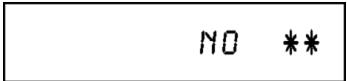 2. Time when the error has occurred is displayed for 5 seconds. 2. Time when the error has occurred is displayed for 5 seconds.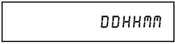 DD: Dayhh: Hourmm: Minute3. Last Drive Error (1/2) is displayed for 5 seconds. DD: Dayhh: Hourmm: Minute3. Last Drive Error (1/2) is displayed for 5 seconds.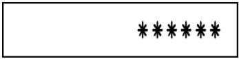 4. Last Drive Error (2/2) is displayed for 5 seconds. 4. Last Drive Error (2/2) is displayed for 5 seconds.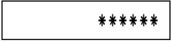 5. Error occurring Disc type is displayed for 5 seconds. 5. Error occurring Disc type is displayed for 5 seconds.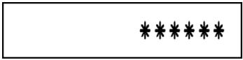 6. Disc Maker ID is displayed for 5 seconds. 6. Disc Maker ID is displayed for 5 seconds.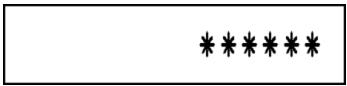 7. Factor of Drive Error occurring is left displayed 7. Factor of Drive Error occurring is left displayed | Press [4] [2] in service mode.When “INFO*****” is being displayed, past 19 error histories can be displayed by pressing [0][1] - [1] [9]In case that the maker cannot be identified, display is black out. |
| Delete the Last Drive Error | Delete the Last Drive Error information stored on the DVD RAM-Drive. |  | Press [9] [6] in service mode. |
| Laser power confirmation | Drive state is judged based on difference between laser power value at shipping and present laser power value. | [CHK * 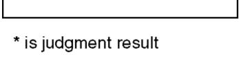 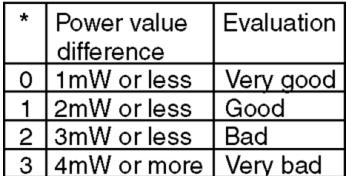 If DVD-RAM disc in not inserted, [NO DISC] is displayed.If power value study was filed, [ERROR] is displayed. If DVD-RAM disc in not inserted, [NO DISC] is displayed.If power value study was filed, [ERROR] is displayed. | 1. Insert DVD-RAM discinto RAM Drive in servicemode. (Other media are assumed to be non-correspondence.)2. Press [4] [4]. |
| Turn on all FL/LEDs | All segments of FL and all LEDs are turned on. |  | Press [5] [1] in service mode. |
| PB HIGH Signal Output | 8 pin of AV 1 Jack (PB HIGH terminal) is High (approx. 11V DC). | Press [5] [2] in service mode. | |
| PB MIDDLE Signal Output | 8 pin of AV 1 Jack (PB HIGH terminal) is Middle (approx. 5.5V DC) | 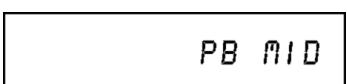 | Press [5] [3] in service mode. |
| Front connection inspection | Press all front keys and check the connection between Main P.C.B. and Front key Switches. | 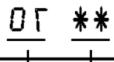 , . , . 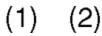 (1) Each time a key is pressed, segment turned on increases one by one.(2) Total umber of keys that have been pressed. (1) Each time a key is pressed, segment turned on increases one by one.(2) Total umber of keys that have been pressed. | Press [5] [4] in service mode. |
| Production Date Display | Display the date when the unit was produced. | 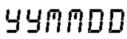 YY: YearMM: MonthDD: Day YY: YearMM: MonthDD: Day | Press [6] [1] in service mode. |
| Display the accumulated working time | Display the accumulated unit's working time. | 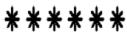 (Indicating unit: Second) (Indicating unit: Second) | Press [6] [4] in service mode. |
| Display the Error History | Display the Error History stored on the unit. | Display reason of error for 5 seconds.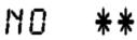 01:Defect of Digital P.C.B.(AV DEC / MAIN CPU)02:Defect of RAM Drive.03:Defect of Disc.04:Defect of Digital P.C.B. or Communication Error.05:Defect of Digital P.C.B.(AV DEC / MAIN CPU)06:Defect of HDD.Display the time when the error has occurred for 5 seconds. 01:Defect of Digital P.C.B.(AV DEC / MAIN CPU)02:Defect of RAM Drive.03:Defect of Disc.04:Defect of Digital P.C.B. or Communication Error.05:Defect of Digital P.C.B.(AV DEC / MAIN CPU)06:Defect of HDD.Display the time when the error has occurred for 5 seconds.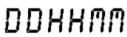 DD: Dayhh: Hourmm: MinuteAccumulated working time till occurring of the error is left displayed. DD: Dayhh: Hourmm: MinuteAccumulated working time till occurring of the error is left displayed. (Indicating unit: Second) (Indicating unit: Second) | Press [6] [5] in service mode. Then press [0] [1] ~ [1] [9], the past 19 error histories are displayed. |
| Delete the Error History | Delete Error History information stored on the unit. |  | Press [9] [7] in service mode. |
| SD card WRITE check | Check SD card WRITE function with SD slot. | When the WRITE check is OK.SD OKWhen the WRITE check is NG.SD NG*Note:The image stored in the SD card will be erased. | Insert a SC card to SD card slot, and press [7] [4] in service mode.* Insert SD card while the power is off.* Check for [CARD SD] display on the FL display and go on the procedure. |
| AV4(V)/AV1(RGB) I/O Setting | Set input to AV4 (V) and set output to AV1 (RGB) for I/O checking | PAL 01 | Press [8] [0] in service mode. |
| AV2(Y/C)/AV1(V) I/O Setting | Set input to AV2 (Y/C) and set output to AV1 (V) for I/O checking | PAL 02 | Press [8] [1] in service mode. |
| AV2(V)/AV1(Y/C) I/O Setting | Set input to AV2 (V) and set output to AV1 (Y/C) for I/O checking | PAL 03 | Press [8] [2] in service mode. |
| AV2(RGB)/AV1(V) I/O Setting | Set input to AV2 (RGB) and set output to AV1 (V) for I/O checking | PAL 04 | Press [8] [3] in service mode. |
| P50(H) Output | Timer Microprocessor IC7501-76 output High signal for AV1-pin 10 passing through inverter (approx. 0V DC at AV1-pin 10). | When OK.PSOHOKWhen NG.PSOHNG | Press [8] [4] in service mode. |
| P50(L) Output | Timer Microprocessor IC7501-76 output Low signal for AV1-pin 10 passing through inverter (approx. 4.4V DC at AV1-pin 10). | When OK.PSOLOKWhen NG.PSOLNG | Press [8] [5] in service mode. |
| Tray OPEN/CLOSE Test | The RAM drive tray is opened and closed repeatedly. | *****"" is number of open/close cycle times. | Press [9] [1] in service mode*When releasing this mode, press the [POWER] button of Remote Controller more than 10 seconds. |
| Error code initialization | Initialization of the last error code held by timer (Write in F00) | CLR | Press [9] [8] in service mode. |
| Initialize Service | Last Drive Error, Error history and Error Codes stored on the unit are initialized to factory setting. | CLR | Press [9] [9] in service mode. |
| Finishing service mode | Release Service Mode. | Display in STOP (E-E) mode.***** | Press power button on the front panel or Remote controller in service mode. |
9 SERVICE FIXTURE AND TOOLS
| Part Number | Description | Compatibility |
| RFKZ0260 | Extension Cable (Main P.C.B. - RAM/Digital P.C.B. / 88 Pin) | Same as EH50 Series |
| RFKZ0216 | Extension Cable (Main P.C.B. - Power P.C.B. / 23 Pin) | Same as E55 Series |
| RFKZ0366 (2x) | Extension FFC (HDMI P.C.B. and HDD - RAM/Digital P.C.B. / 40 Pin / 500 mm) | Same as EH55 / EH56 Series |
| RFKZ0168 | Extension Cable (Power P.C.B. - Fan Motor / 3 Pin) | Same as E50 / E55 Series |
| RFKZ0339 | Extension Cable (Main P.C.B. - HDD / 4 Pin) | Same as EH55 / EH56 Series |
| JZS0484 | Eject Pin | Same as ES15 |
| RFKZ03D01K | Lead Free Solder (0.3 mm / 100 g Reel) | Same as ES15 |
| RFKZ06D01K | Lead Free Solder (0.6 mm / 100 g Reel) | Same as ES15 |
| RFKZ010D01 | Lead Free Solder (1.0 mm / 100 g Reel) | Same as ES15 |
| RFKZ0316 | Solder Remover (Lead free 10 W temperature Solder / 180 g) | Same as ES15 |
| RFKZ0328 | Flux | Same as ES15 |
| RFKZ0329 | Bottle of Flux | Same as ES15 |
10 ASSEMBLING AND DISASSEMBLING
Caution: Original screws should be used.
10.1. DISASSEMBLY FLOW CHART
This chart is the procedure for disassembling the casing and inside parts for internal inspection when carrying out the servicing. To assemble the unit, reverse the steps shown in the chart below.
![graph TD A["10.3 TOP CASE"] --> B["10.8 HARD DISC DRIVE"] A --> C["10.4 FRONT PANEL"] A --> D["10.9 POWER P.C.B."] A --> E["10.10 REAR PANEL AND FAN MOTOR"] A --> F["10.11 BACK END P.C.B."] B --> G["10.5 SD CARD P.C.B."] C --> H["10.6 RAM/DIGITAL P.C.B. MODULE"] D --> I["11.13 TUNER P.C.B. AND TUNER…](/content/2019/11/105906/images/62b0d7cf014e17df94766b5876b6f3b8b881d6d4fb16cdda7f726cf2ef9bc042.jpg)
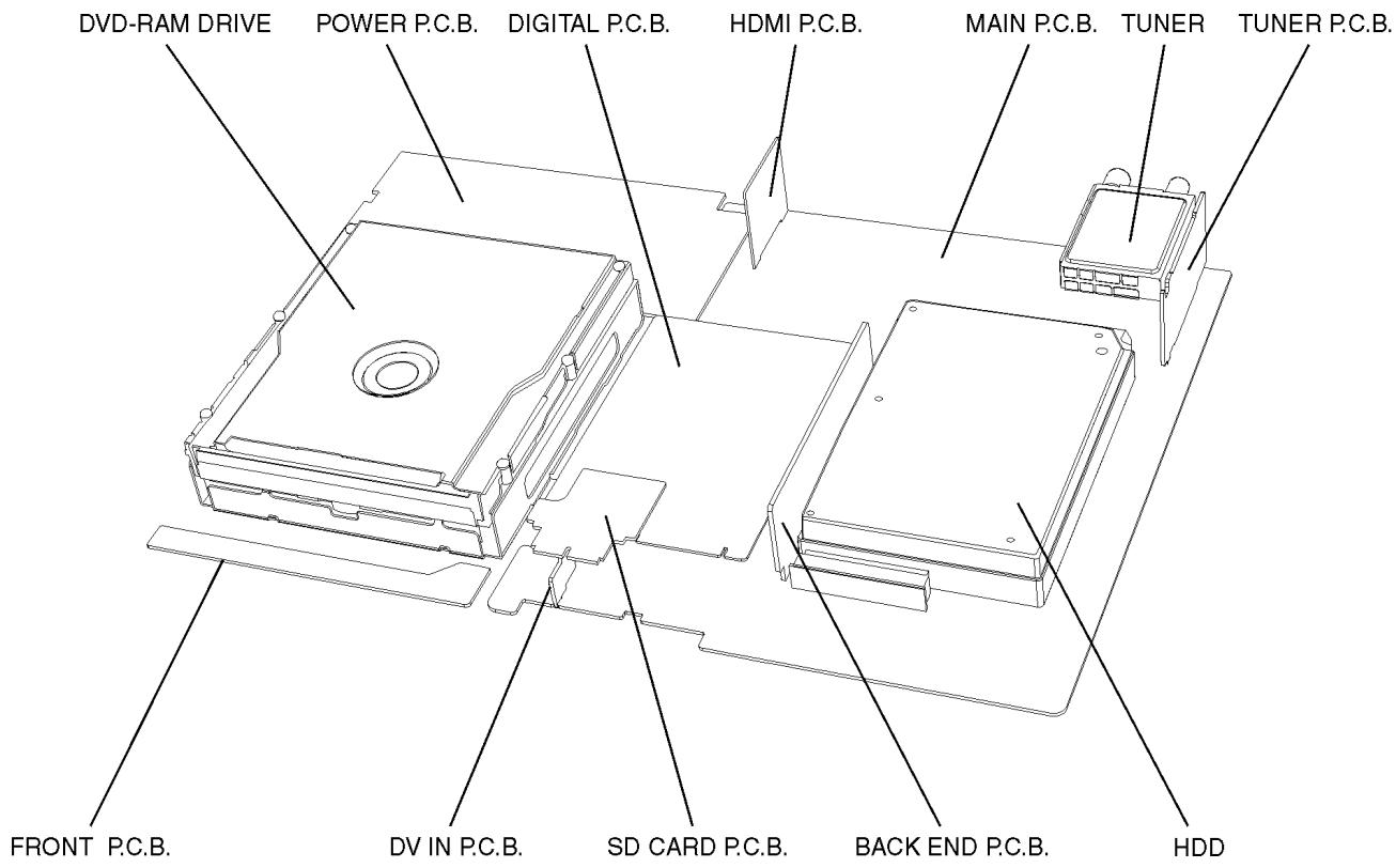
10.2. P.C.B. POSITIONS
10.3. TOP CASE
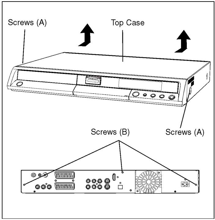
- Remove the 2 screws (A) and 3 screws (B).
- Slide Top Case rearward and open the both ends at rear side of the Top Case a little and lift the Top Case in the direction of the arrows.
10.4. FRONT PANEL
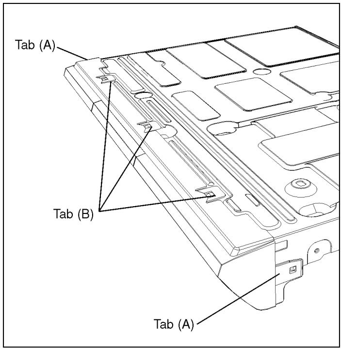
- Unlock 2 tabs (A) and 3 tabs (B) in this order to remove Front Panel.
The tab (A) and (B) should be unlocked at the same time, respectively.
10.5. SD CARD P.C.B.
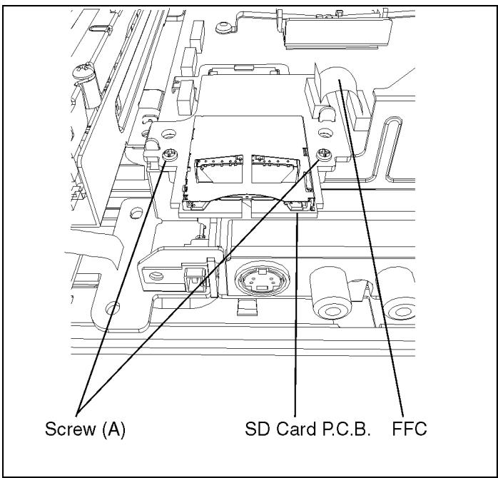
- Release FFC
- Remove 2 Screws (A) to remove SD Card P.C.B. .
Caution:
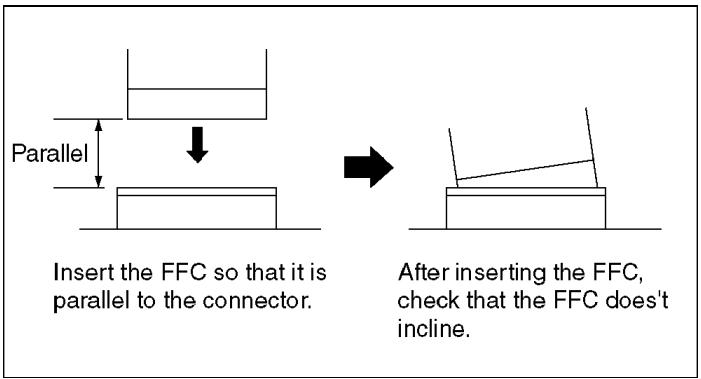
When replacing SD Card P.C.B., pay attention as below.
10.6. RAM/DIGITAL P.C.B. MODULE
Caution:
Pairing of RAM Drive and Digital P.C.B. as “RAM / Digital P.C.B. Module” have to be replaced together. If the pairing is changed, RAM Drive unit has to be re-aligned. Because the alignment data for RAM Drive Unit is stored in Digital P.C.B.
Note:
When replacing the Digital P.C.B., “UNFORMAT” indication is displayed and HDD must be formatted.
After that all programme in the HDD will be lost.
How to format the HDD.
- After “UNFORMAT” is displayed on the FL display, warning message for HDD format is appeared on the TV screen.
- Select "YES" and press "ENTER" button on the remote control; the HDD will be formatted automatically. • After that all programme in the HDD will be lost.
Caution:
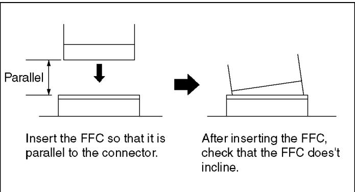
When replacing Digital P.C.B., pay attention as below.
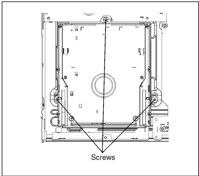
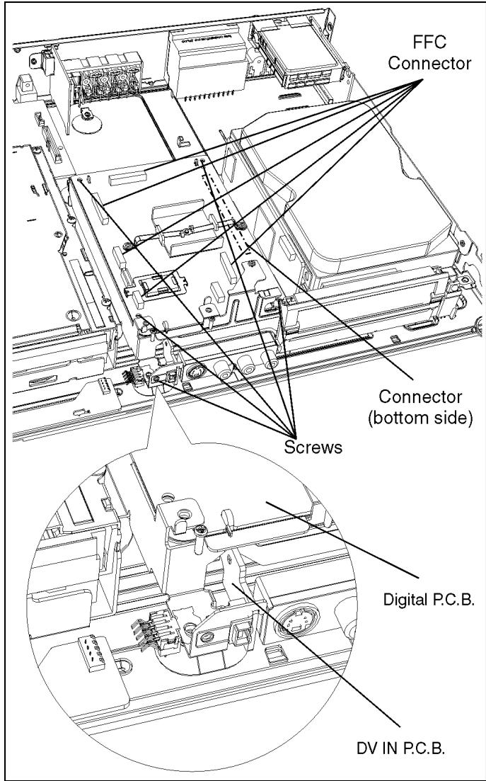
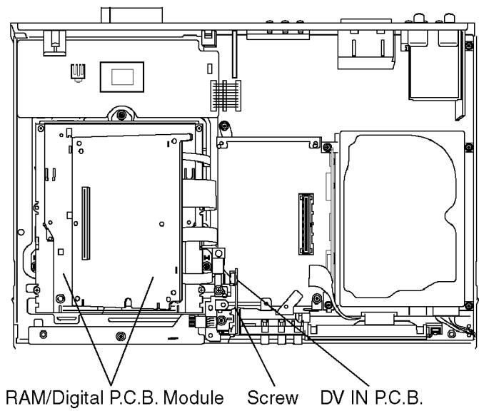
- Remove 3 Screws on DVD-RAM Drive.
- Remove 2 FFCs and 4 Screws.
- Lift up Digital P.C.B. slightly to disconnect Main P.C.B. Connector and DV IN P.C.B. Connector on the bottom side.
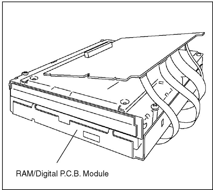
- Put Digital P.C.B. on DVD-RAM Drive and remove RAM/Digital P.C.B. Module.
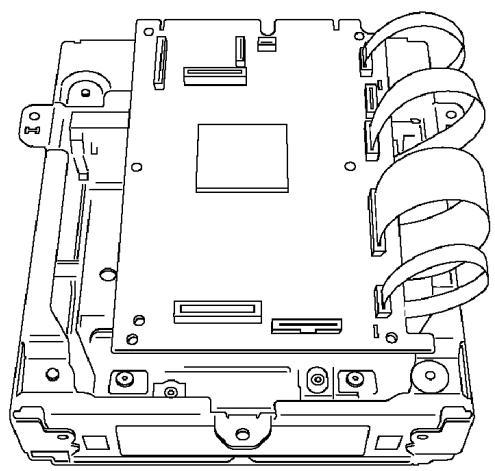
Note:
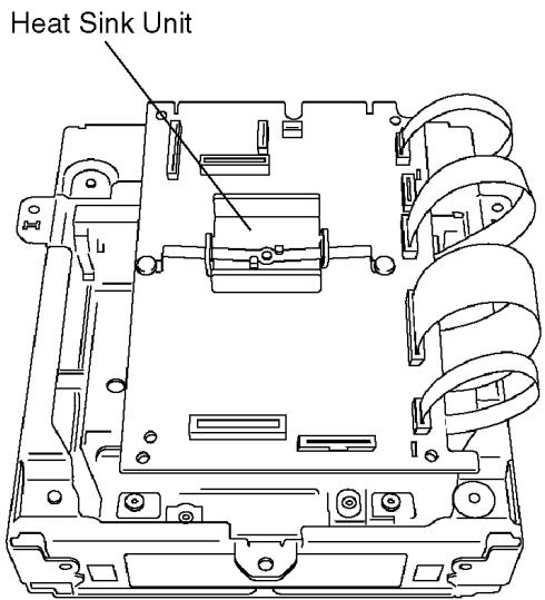
RAM/Digital P.C.B. Module as service part has no heat sink unit. Before returning to customer, heat sink unit should be installed on to Digital P.C.B.

10.7. DV IN P.C.B.
- Remove 1 Screw to remove DV IN P.C.B.
10.8. HARD DISC DRIVE
Caution:
Writing the main firmware to the unit is necessary after replacing the HDD. Prepare the latest firmware updating disc.
* The main firmware is recorded in the HDD, but the replacement HDD has no data (and needs to be formatted).
Writing Procedure of Main Firm:
- Writing of Main Firm needs 3, 4 minutes.
- Never cut the power of DVD Recorder until writing in Firmware ends.
- Initial settings and contents of reservation will not change if writing is normally completed.
- Prepare latest firmware updating disc
- Replace HDD
- Turn on power of DVD Recorder
- After [PLEASE WAIT] is displayed on FL., [HDD ERR] is displayed on FL
- Tray opens automatically
- Insert updating disc for Firmware and press OPEN / CLOSE key (If a wrong disc was inserted, [NG DISK] [NO FVU] is displayed on FL.)
- [LOAD] → [LD FVU] ←→ [M_FIRM] are displayed on FL alternately
- [MAIN] ↔ [UPD OK] blink alternately and Tray opens. Take out disc (Writing was finished)
- Press Power button to turn off power
- Press Power button to turn on power
- [HELLO] → [SELF CHECK] are displayed on FL
- [UNFORMATED] is displayed on FL
- After [UNFORMAT] was displayed, message to request FORMAT is displayed on TV screen
- Select [Yes] and press [ENTER] key to format HDD (After FORMAT, program in HDD will be lost, but Main firm will not be lost "Write of the main farm" is completed above
* Drive firm is not updated by above operation. If you wish update Drive firm, please prepare the disc for latest firmware update, and write again. * If the version of the firm you have prepared was same as or later than has already been written in deck, “UNSUPPORT” is displayed on FL. * In a usual updating of firmware, writing is not performed when the timer reservation standby was not released.
- Remove ATAPI Connector and HDD Power Connector.
- Remove 4 Screws (A) to remove HDD Angle with HDD.
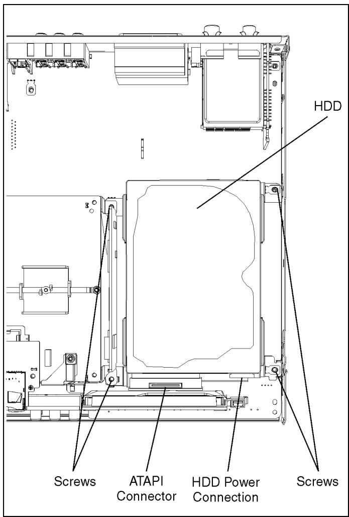
- Put HDD with Angle up side down not to give a shock to HDD.
- Remove 2 screws to remove HDD.
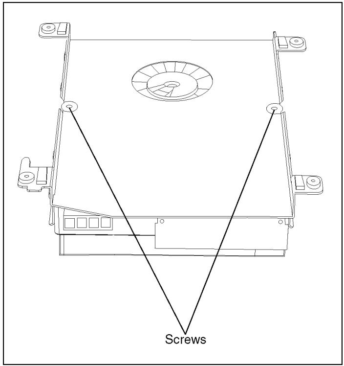
Handling of HDD
The following precautions should be taken when handling HDD.
a. Never give an impact to HDD. (Even a drop from 1 cm height can be a cause of HDD failure). b. When placing HDD on a workbench, provide a mat on a bench for shock absorption and anti-static purposes. c. When installing HDD, release it from your hands only after confirming that it is fully set on the chassis. d. Avoid stacking up HDD. e. HDD is unstable and easy to fall. Do not stand it on its side face. f. When handling HDD, hold its side faces to avoid static hazard. g. Do not place HDD on its wrapping bag after removal. (Prevention of static hazard.) h. Use a screwdriver with low impact and anti-static features.
Note:
When replacing HDD, please make the rear jumper slave or cable select configuration.
10.9. POWER P.C.B.
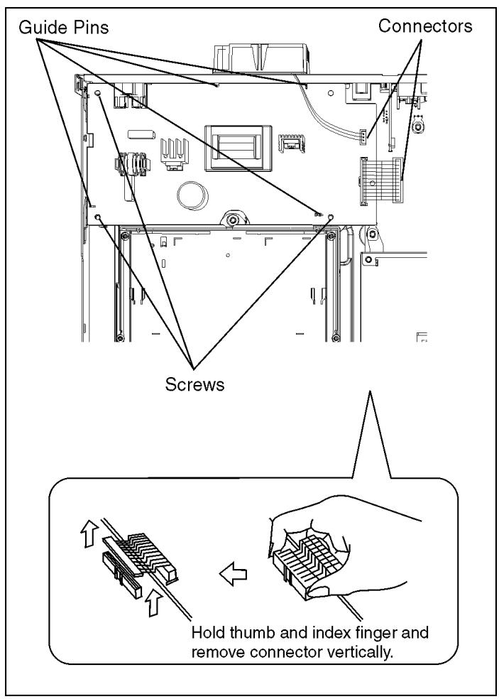
- Remove the Screw (AC Inlet).
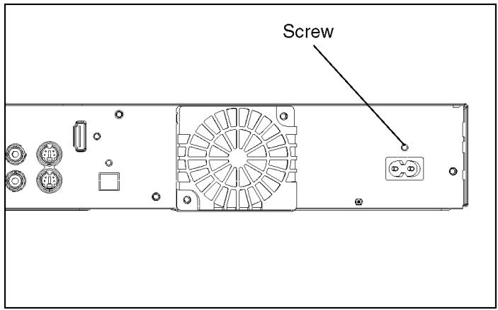
- Remove 3 Screws and disconnect the 2 Connectors.
- Lift up Power P.C.B. a little upwards and remove the P.C.B. sideways out of the Guide Pins.
Note:
When inserting P.C.B. confirm correct positions of Guide Pins.
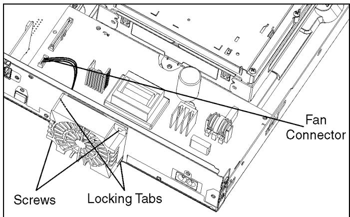
10.10. REAR PANEL
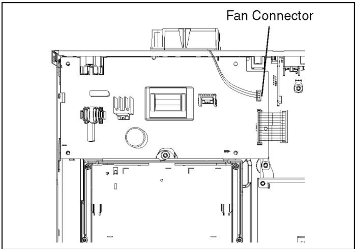
- Disconnect Fan Connector.
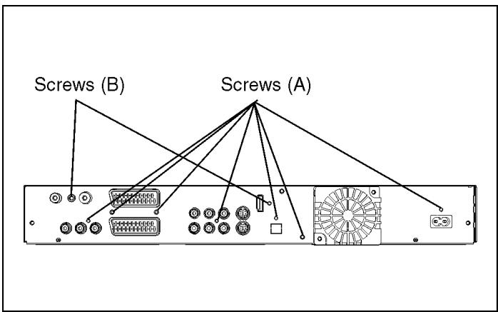
- Remove 7 Screws (A) and 2 Screws (B).
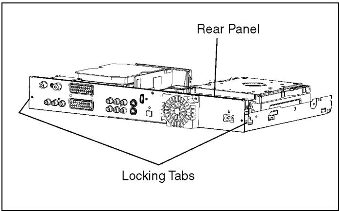
- Unlock 2 Locking Tabs to remove Rear Panel.
10.10.1. FAN MOTOR
- Disconnect Fan Connector.
- Remove the 2 Screws.
- Push and unlock 2 locking Tabs to remove Fan Motor.
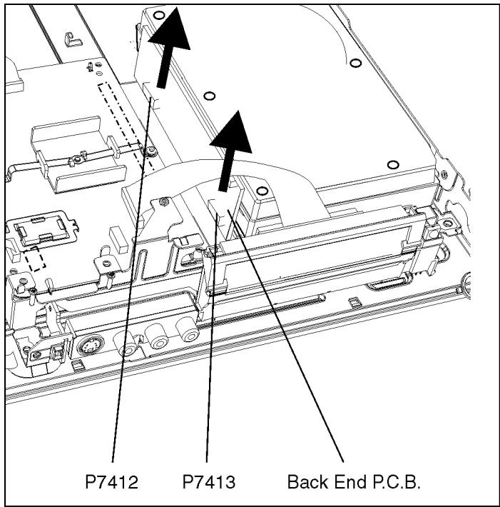
10.11. BACK END P.C.B.
- Pull out the Back End P.C.B. in the direction to the arrow.
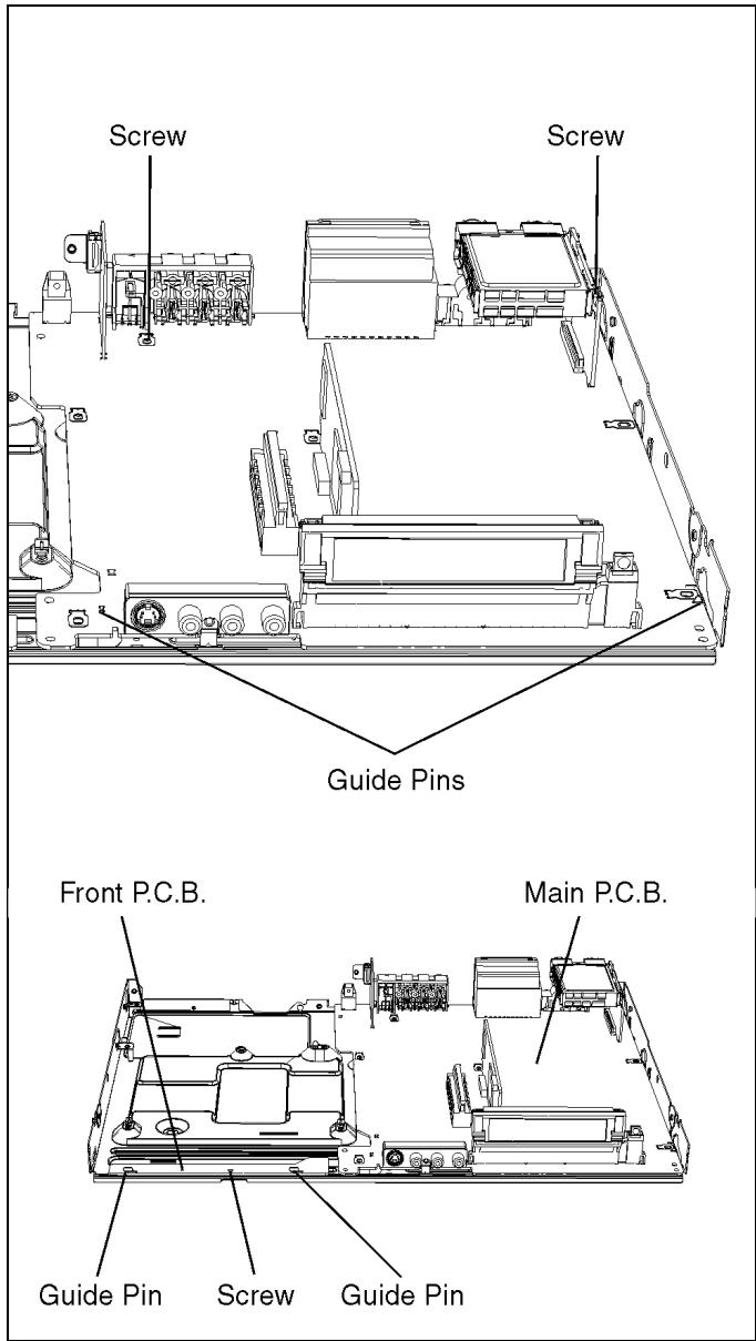
10.12. MAIN P.C.B. AND FRONT P.C.B.
- Remove 2 Screws from Main P.C.B. .
- Remove 1 Screw from Front P.C.B. .
- Pull out Main P.C.B. together with Front P.C.B. .
Note:
When inserting P.C.B., confirm correct positions of Guide Pins.
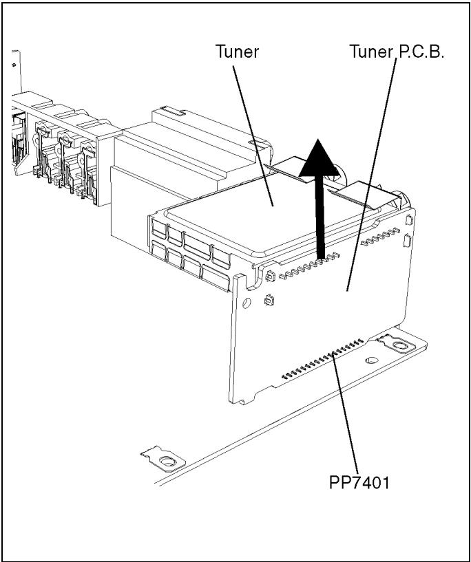
10.13. TUNER P.C.B. AND TUNER
- Pull out the Tuner P.C.B. in the direction of the arrow.
- Remove solder and pull out Tuner from Tuner P.C.B.
10.14. HDMI P.C.B.
- Disconnect FFC connector.
- Pull out the HDMI P.C.B. in the direction of the arrow.
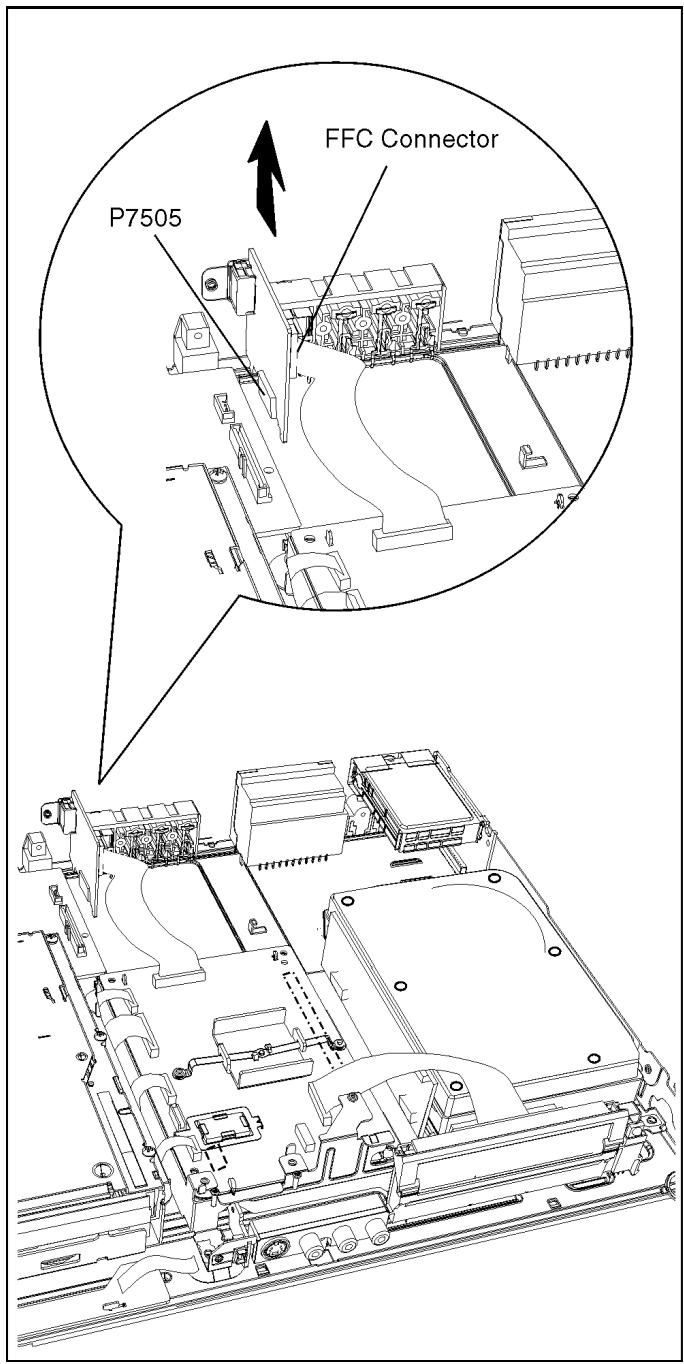
Caution:
When replacing HDMI P.C.B., pay attention as below.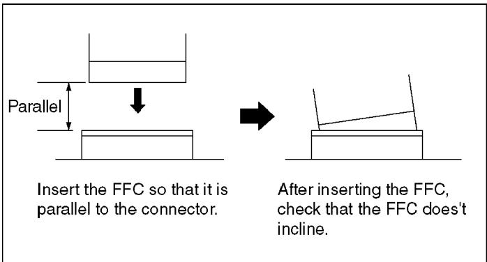
11 MEASUREMENTS AND ADJUSTMENTS
11.1. SERVICE POSITIONS
Note:
For description of the disassembling procedure, see the section ASSEMBLING AND DISASSEMBLING (DISASSEMBLY FLOW CHART).
11.1.1. CHECKING AND REPAIRING OF POWER P.C.B.
1. Top Case
- Remove 2 Screws (A) on side
- Remove 3 rear Screws (B) on rear
- Remove Top Case
2. Power P.C.B.
- Remove 1 Screw for AC Inlet fixing
- Remove 3 Screws fixing Power P.C.B.
- Remove 1 Connector to Main P.C.B.
- Remove 1 Connector to Fan P.C.B.
- Lift up Power P.C.B. sideways out of the Guide Pins.
- Connect Extension Cable: – between Main P.C.B. and Power P.C.B. with RFKZ0216 – between Fan Motor and Power P.C.B. with RFKZ0168
- Put Power P.C.B. on Insulation Board so that it's solder side faces top
Caution 1
Red wire in the extension cable should be connected to pin 1
Caution 2
Original screws should be used
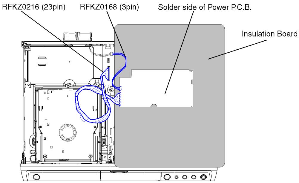
11.1.2. CHECKING AND REPAIRING OF MAIN P.C.B.
1. Top Case
- Remove 2 Screws (A) on side and 3 rear Screws (B)
- Remove Top Case
2. Front Panel
- Unlock 2 Locking Tabs on the side and 3 Locking Tabs on bottom
- Remove Front Panel
3. Rear Panel with Fan Motor
- Remove 7 Screws (A) and 2 Screws (B)
- Unlock 2 Locking Tabs to remove Rear Panel
4. Power P.C.B.
- Remove 3 Screws fixing Power P.C.B.
- Unlock Connector to Main P.C.B.
- Remove Power P.C.B. together with Rear Panel
5. Hard Disc Drive
- Remove 4 Screws fixing Hard Disc Drive Angle
6. Digital P.C.B. with SD Card P.C.B. and DV IN P.C.B.
- Remove 2 Screws fixing Digital P.C.B. Angle
7. Main P.C.B.
- Remove 2 Screws from Main P.C.B.
- Remove Screw from Front P.C.B.
- Unlock Main P.C.B. and Front P.C.B. from Bottom Plate
- Hold Hard Disc Drive and Digital P.C.B. carefully and put it together with Main P.C.B. up side down on the Insulation Board.
- Connect the Extension Cable: – between Main P.C.B. and Power P.C.B. with RFKZ0216
Caution 1
Red wire in the extension cable should be connected to (1) pin.
Caution2
Original screws should be used.
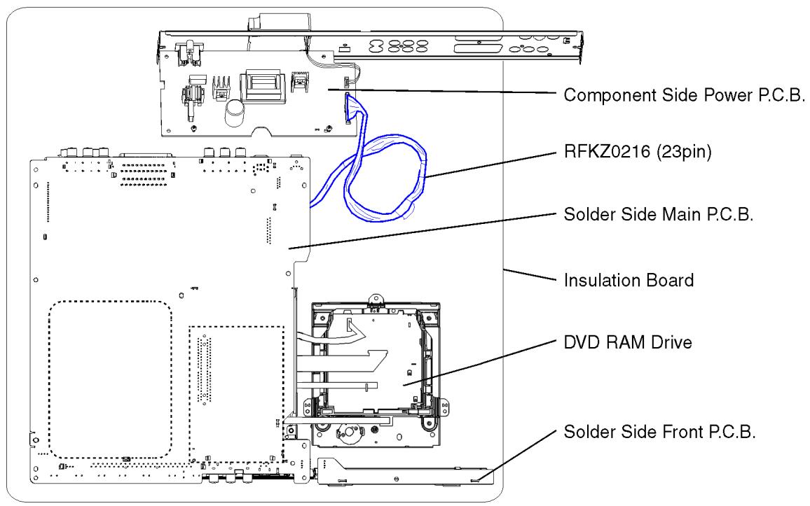
11.1.3. CHECKING AND REPLACING OF DVD-RAM DRIVE
1. Top Case
- Remove 2 Screws (A) on side and 3 rear Screws (B)
- Remove Top Case
2. Front Panel
- Unlock 2 Locking Tabs on side and 3 Locking Tabs on bottom
- Remove Front Panel
3. SD Card P.C.B.
- Remove 2 Screws
- Lift up SD Card P.C.B. and wrap it with insulation sheet.
4. HDD
- Remove 4 Screws fixing HDD Angle to remove it with HDD
- Disconnect FFC from HDD
5. RAM/Digital P.C.B. Module
- Remove 4 Screws fixing DVD-RAM Drive
- Disconnect FFC from HDMI P.C.B.
- Lift up Digital P.C.B. slightly to disconnect Main P.C.B. Connector and DV IN P.C.B. Connector on the bottom side. • Take DV IN P.C.B. out of the Main P.C.B. and attach it to the Digital P.C.B.
- Put RAM/Digital P.C.B. Module on the side.
Connect Extension Cable:
– between Main P.C.B. and DVD-RAM Drive with RFKZ0260 – between Hard Disc Drive and Digital P.C.B. with FFC Extension Cable RFKZ0366 – between HDMI P.C.B. and Digital P.C.B. with FFC Extension Cable RFKZ0366
Caution
Original screws should be used.
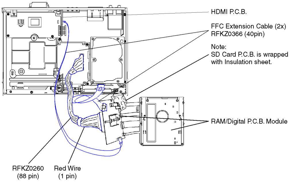
11.1.4. CHECKING AND REPLACING OF HARD DISC DRIVE
1. Top Case
- Remove 2 Screws (A) on side
- Remove 3 rear Screws (B) on rear
- Remove Top Case
2. Hard Disc Drive
- Remove 4 Screws of HDD Angle from Main P.C.B.
- Remove HDD ATAPI Connector
- Remove Power Cable from HDD
- Remove 2 Screws from HDD to disconnect HDD Angle
- Put Replacement HDD on Insulation Board
- Connect Extension Cable:
– between Main P.C.B. and HDD with RFKZ0339 – between Digital P.C.B. and HDD with FFC Extension Cable RFKZ0366
Caution
Original screws should be used.
Caution for Removing Hard Disc Drive
Put HDD with HDD Angel up side down and remove the screws without giving a shock to HDD.
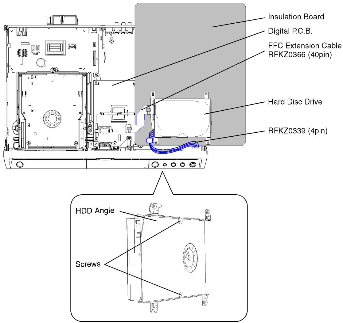
11.2. CAUTION FOR REPLACING PARTS
11.2.1. ITEMS THAT SHOULD BE DONE AFTER REPLACING PARTS
√: Necessary — : Unnecessary
| Items that Should be doneReplacing Parts | Reset IC7501* Note 1 | Obtain and register a new registration code (Except EX75EB/EX85EB)* Note 2 | Main Firm update* Note 3 | HDD Format |
| Main P.C.B. | ✓ | ✓ | - | ✓ |
| IC7501 (Timer IC) | ✓ | - | - | - |
| IC7404 (EEPROM) | - | ✓ | - | ✓ |
| HDD | - | - | ✓ | ✓ |
* Note 1: (Resetting Method)
| Resetting object | Condition of power | Short Terminal |
| IC7501 (Timer IC) | POWER ON | IC7502-4 (Reset_L) and (GND) |
* Note 2:
Please always pass the customer “Warning for Customers Who Use the DivX Video-on-Demand content.” with the product and get it when you unavoidably exchange EEPROM or P.C.B. including EEPROM (When the product is exchanged, it is the same.).
You must use print attached to service part (EEPROM or P.C.B. including EEPROM) or must use copy of print below as "Warning for Customers who use the DivX Video-on-Demand content." Information needed without fail for the customer for whom it is used continuing DivX Video-on-Demand Service to "Manual for the customer" is recorded.
Appendix:* Parts that memorize user's information are only EEPROM.* The registration of Registration Code is possible for half a year up to 6 recorders up to 10 recorders a year. Replacement of EEPROM or P.C.B. including EEPROM spends one of this.
Registration Code is memorized in EEPROM (RFKxxxxxx).
Model without VHS: on Main P.C.B. Model with VHS: on Digital I/F P.C.B. (Power & DVD I/F/P.C.B.) If exchange above P.C.B. or EEPROM, new registration Code differ from previous Registration Code will be generated. In this case if your customer uses DivX Video-on-Demand service, he/she will no longer be able to play any content that he/she purchased under that same registration code. Therefore your customer will need to obtain and register the new registration code.
*Copy this page and cut on the dotted line and give the lower half to your customer.
Warning for Customers who use the DivX Video-on-Demand content.
- The registration code has been changed for the repair of the product or the product exchange.
- Obtain and register a new registration code, otherwise you will no longer be able to play DivX Video-on-Demand content.
- Follow the procedure on the DivX Video-on-Demand web site to register at http://vod.divx.com/ * If you do not use the DivX Video-on-Demand content, please ignore this warning.
* Note 3:
Please prepare latest firmware updating disc.
*Main Firm is being recorded in HDD, but new HDD has no data.
CAUTION:
- Writing of Main Firm needs 3, 4 minutes.
- Never cut the power of DVD Recorder until writing in Firmware ends.
- Initial settings and contents of reservation will not change if writing is normally completed.
Writing Procedure of Main Film:
- Prepare updating disc for firmware.
- Replace HDD.
- Turn on power of DVD Recorder.
- After [PLEASE WAIT] is displayed on FL., [HDD ERR] is displayed on FL.
- Tray opens automatically.
- Insert updating disc for firmware and press OPEN / CLOSE key. (If a wrong disc was inserted, [NG DISK] [NO FVU] is displayed on FL.)
- [LOAD] → [LD FVU] ←→ [M_FIRM] are displayed on FL alternately.
- [MAIN] ↔ [UPD OK] blink alternately and tray opens. Take out disc. (Writing was finished.)
- Press Power button to turn off power.
- Press Power button to turn on power.
- [HELLO] → [SELF CHECK] are displayed on FL.
- [UNFORMATED] is displayed on FL.
- After [UNFORMAT] was displayed, message to request FORMAT is displayed on TV screen.
- Select [Yes] and press [ENTER] key to format HDD.
(After FORMAT, program in HDD will be lost, but Main firmware will not be lost.)
"Write of the main firmware" is completed above
* Drive firmware is not updated by the above operation. If you wish to update the drive firmware, please prepare the disc for the latest firmware update, and write again. * If the version of the firmware you have prepared was the same as or later than what has already been written in the deck, "UNSUPPORT" is displayed on FL. * In a usual firmware update, writing is not performed when the timer reservation standby was not released.
11.2.2. NOTICE AFTER REPLACING RAM/DIGITAL P.C.B. MODULE
After replacing the RAM/Digital P.C.B. Module, "TM AV1" is displayed on FL. Once power off, and start-up again.
11.3. STANDARD INSPECTION SPECIFICATIONS AFTER MAKING REPAIRS
After making repairs, we recommend performing the following inspection to check normal operation.
| No. | Procedure | Item to Check |
| 1 | Turn on the power, and confirm items pointed out. | Items pointed out should reappear. |
| 2 | Insert RAM disc. | The Panasonic RAM disc should be recognized. |
| 3 | Enter the EE (TU IN / AV IN - AV OUT) mode. | No abnormality should be seen in the picture, sound or operation. |
| 4 | Perform auto recording and playback for one minute using the RAM disc. | No abnormality should be seen in the picture, sound or operation.*Panasonic DVD-RAM disc should be used when recording and playback. |
| 5 | If a problem is caused by a VCD, DVD-R, DVD-Video, Audio-CD, or MP3, playback the test disc. | No abnormality should be seen in the picture, sound or operation. |
| 6 | After checking and making repairs, upgrade the firmware to the latest version. | Make sure that [UPD OK] appears in the FL displays. |
| 7 | Transfer [9][9] in the service mode setting, and initialize the service settings (return various settings and error information to their default values. The laser time is not included in this initialization). | Make sure that [CLR] appears in the FL display.After checking it, turn the power off. |
| 8 | After checking and making repairs, upgrade the firmware to the latest version. | Make sure that [UPD OK] appears in the FL displays.*[UNSUPPORT] display means the unit is already updated to newest same version. Then version up is not necessary. |
| 9 | Transfer [9][9] in the service mode setting, and initialize the service settings (return various settings and error information to their default values. The laser time is not included in this initialization). | Make sure that [CLR] appears in the FL display.After checking it, turn the power off. |
| 10 | When replacing of RAM drive, transfer [9] [5] in the service mode setting to delete Laser used time. | Make sure that [CLR] appears in the FL display.After that, turn power off. |
Use the following checklist to establish the judgement criteria for the picture and sound.
| Item | Contents | Check | Item | Contents | Check |
| Picture | Block noise | Sound | Distorted sound | ||
| Crosscut noise | Noise (static, background noise, etc.) | ||||
| Dot noise | The sound level is too low. | ||||
| Picture disruption | The sound level is too high. | ||||
| Not bright enough | The sound level changes. | ||||
| Too bright | |||||
| Flickering color | |||||
| Color fading |
11.4. ABBREVIATIONS
| INITIAL/LOGO | ABBREVIATIONS | |
| A | A0~UP | ADDRESS |
| ACLK | AUDIO CLOCK | |
| AD0~UP | ADDRESS BUS | |
| ADATA | AUDIO PES PACKET DATA | |
| ALE | ADDRESS LATCH ENABLE | |
| AMUTE | AUDIO MUTE | |
| AREQ | AUDIO PES PACKET REQUEST | |
| ARF | AUDIO RF | |
| ASI | SERVO AMP INVERTED INPUT | |
| ASO | SERVO AMP OUTPUT | |
| ASYNC | AUDIO WORD DISTINCTION SYNC | |
| B | BCK | BIT CLOCK (PCM) |
| BCKIN | BIT CLOCK INPUT | |
| BDO | BLACK DROP OUT | |
| BLKCK | SUB CODE BLOCK CLOCK | |
| BOTTOM | CAP. FOR BOTTOM HOLD | |
| BYP | BYPATH | |
| BYTCK | BYTE CLOCK | |
| C | CAV | CONSTANT ANGULAR VELOCITY |
| CBDO | CAP. BLACK DROP OUT | |
| CD | COMPACT DISC | |
| CDSCK | CD SERIAL DATA CLOCK | |
| CDSRDATA | CD SERIAL DATA | |
| CDRF | CD RF (EFM) SIGNAL | |
| CDV | COMPACT DISC-VIDEO | |
| CHNDATA | CHANNEL DATA | |
| CKSL | SYSTEM CLOCK SELECT | |
| CLV | CONSTANT LINEAR VELOCITY | |
| COFTR | CAP. OFF TRACK | |
| CPA | CPU ADDRESS | |
| CPCS | CPU CHIP SELECT | |
| CPDT | CPU DATA | |
| CPUADR | CPU ADDRESS LATCH | |
| CPUADT | CPU ADDRESS DATA BUS | |
| CPUIRQ | CPU INTERRUPT REQUEST | |
| CPRD | CPU READ ENABLE | |
| CPWR | CPU WRITE ENABLE | |
| CS | CHIP SELECT | |
| CSYNCIN | COMPOSITE SYNC IN | |
| CSYNCOUT | COMPOSITE SYNC OUT | |
| D | DACCK | D/A CONVERTER CLOCK |
| DEEMP | DEEMPHASIS BIT ON/OFF | |
| DEMPH | DEEMPHASIS SWITCHING | |
| DIG0~UP | FL DIGIT OUTPUT | |
| DIN | DATA INPUT | |
| DMSRCK | DM SERIAL DATA READ CLOCK | |
| DMUTE | DIGITAL MUTE CONTROL | |
| DO | DROP OUT | |
| DOUT0~UP | DATA OUTPUT | |
| DRF | DATA SLICE RF (BIAS) | |
| DRPOUT | DROP OUT SIGNAL | |
| DREQ | DATA REQUEST | |
| DRESP | DATA RESPONSE | |
| DSC | DIGITAL SERVO CONTROLLER | |
| DSLF | DATA SLICE LOOP FILTER | |
| DVD | DIGITAL VIDEO DISC | |
| E | EC | ERROR TORQUE CONTROL |
| ECR | ERROR TORQUE CONTROL | |
| REFERENCE | ||
| ENCSEL | ENCODER SELECT | |
| ETMCLK | EXTERNAL M CLOCK (81MHz/40.5MHz) | |
| ETSCLK | EXTERNAL S CLOCK (54MHz) | |
| F | FBAL | FOCUS BALANCE |
| FCLK | FRAME CLOCK | |
| FE | FOCUS ERROR | |
| FFI | FOCUS ERROR AMP INVERTED INPUT | |
| FEO | FOCUS ERROR AMP OUTPUT | |
| FG | FREQUENCY GENERATOR | |
| FSC | FREQUENCY SUB CARRIER | |
| FSCK | FS (384 OVER SAMPLING) CLOCK | |
| G | GND | COMMON GROUNDING (EARTH) |
| H | HA0~UP | HOST ADDRESS |
| HD0~UP | HOST DATA | |
| HINT | HOST INTERRUPT | |
| HRXW | HOST READ/WRITE | |
| INITIAL/LOGO | ABBREVIATIONS | |
| I | IECOUTIPFRAGIREFISEL | IEC958 FORMAT DATA OUTPUTINTERPOLATION FLAGI (CURRENT) REFERENCEINTERFACE MODE SELECT |
| L | LDONLPCLRCK | LASER DIODE CONTROLLASER POWER CONTROLL CH/R CH DISTINCTION CLOCK |
| M | MA0~UPMCKMCKIMCLKMDATAMDQ0~UPMDQMMLDMPEG | MEMORY ADDRESSMEMORY CLOCKMEMORY CLOCK INPUTMEMORY SERIAL COMMAND CLOCKMEMORY SERIAL COMMAND DATAMEMORY DATA INPUT/OUTPUTMEMORY DATA I/O MASKMEMORY SERIAL COMMAND LOADMOVING PICTURE EXPERTS GROUP |
| O | ODCOFTROSCIOSCOOSD | OPTICAL DISC CONTROLLEROFF TRACKINGOSCILLATOR INPUTOSCILLATOR OUTPUTON SCREEN DISPLAY |
| P | P1~UPPCDPCKPDVDPEAKPLLCLKPLLOKPWMCTLPWMDAPWMOA, B | PORTCD TRACKING PHASE DIFFERENCEPLL CLOCKDVD TRACKING PHASE DIFFERENCECAP. FOR PEAK HOLDCHANNEL PLL CLOCKPLL LOCKPWM OUTPUT CONTROLPULSE WAVE MOTOR DRIVE APULSE WAVE MOTOR OUT A, B |
| R | RERFENVRFORSRSELRSTRSV | READ ENABLEERF ENVELOPERF PHASE DIFFERENCE OUTPUT(CD-ROM) REGISTER SELECTRF POLARITY SELECTRESETRESERVE |
| S | SBIO, 1SBO0SBTO, 1SCKSCKRSCLSCLKSDASEGO~UPSELCLKSENSIN1, 2SOUT1, 2SPDISPDOSPENSPRCLKSPWCLKSQCKSQCXSRDATASRMADRSRMDT0~7SSSTATSTCLKSTD0~UPSTENABLESTSELSSTVALIDSUBCSBCKSUBQSYSCLK | SERIAL DATA INPUTSERIAL DATA OUTPUTSERIAL CLOCKSERIAL DATA CLOCKAUDIO SERIAL CLOCK RECEIVERSERIAL CLOCKSERIAL CLOCKSERIAL DATAFL SEGMENT OUTPUTSELECT CLOCKSERIAL PORT ENABLESERIAL DATA INSERIAL DATA OUTSERIAL PORT DATA INPUTSERIAL PORT DATA OUTPUTSERIAL PORT R/W ENABLESERIAL PORT READ CLOCKSERIAL PORT WRITE CLOCKSUB CODE Q CLOCKSUB CODE Q DATA READ CLOCKSERIAL DATASRAM ADDRESS BUSSRAM DATA BUS 0~7START/STOPSTATUSSTREAM DATA CLOCKSTREAM DATASTREAM DATA INPUT ENABLESTREAM DATA POLARITY SELECTSTREAM DATA VALIDITYSUB CODE SERIALSUB CODE CLOCKSUB CODE Q DATASYSTEM CLOCK |
| T | TE | TRACKING ERROR |
| TIBAL | BALANCE CONTROL | |
| TID | BALANCE OUTPUT 1 | |
| TIN | BALANCE INPUT | |
| TIP | BALANCE INPUT | |
| TIS | BALANCE OUTPUT 2 | |
| TPSN | OP AMP INPUT | |
| TPSO | OP AMP OUTPUT | |
| TPSP | OP AMP INVERTED INPUT | |
| TRCRS | TRACK CROSS SIGNAL | |
| TRON | TRACKING ON | |
| TRSON | TRAVERSE SERVO ON | |
| V | VBLANK | V BLANKING |
| VCC | COLLECTOR POWER SUPPLY VOLTAGE | |
| VCDCONT | VIDEO CD CONTROL (TRACKING BALANCE) | |
| VDD | DRAIN POWER SUPPLY VOLTAGE | |
| VFB | VIDEO FEED BACK | |
| VREF | VOLTAGE REFERENCE | |
| VSS | SOURCE POWER SUPPLY VOLTAGE | |
| W | WAIT | BUS CYCLE WAIT |
| WDCK | WORD CLOCK | |
| WEH | WRITE ENABLE HIGH | |
| WSR | WORD SELECT RECEIVER | |
| X | X | X' TAL |
| XALE | X ADDRESS LATCH ENABLE | |
| XAREQ | X AUDIO DATA REQUEST | |
| XCDROM | X CD ROM CHIP SELECT | |
| XCS | X CHIP SELECT | |
| XCSYNC | X COMPOSITE SYNC | |
| XDS | X DATA STROBE | |
| XHSYNCO | X HORIZONTAL SYNC OUTPUT | |
| XHINT | XH INTERRUPT REQUEST | |
| XI | X' TAL OSCILLATOR INPUT | |
| XINT | X INTERRUPT | |
| XMW | X MEMORY WRITE ENABLE | |
| XO | X' TAL OSCILLATOR OUTPUT | |
| XRE | X READ ENABLE | |
| XSRMCE | X SRAM CHIP ENABLE | |
| XSRMOE | X SRAM OUTPUT ENABLE | |
| XSRMWE | X SRAM WRITE ENABLE | |
| XVCS | X V-DEC CHIP SELECT | |
| XVDS | X V-DEC CONTROL BUS STROBE | |
| XVSYNCO | X VERTICAL SYNC OUTPUT | |
12 BLOCK DIAGRAM
12.1. POWER BLOCK DIAGRAM
![graph TD A["AC INLET P110"] --> B["250V T2AL F1101"] B --> C["SURGE SUPpressor AND SURGE ABSORBER"] C --> D["D140.C1143"] D --> E["RECTIFIER"] E --> F["T1150 POWER SWITCHING TRANSFORMER"] F --> G["P1"] G --> H["IC1150 (SWITCHING IC)"] H --> I["F/B"] I --> J["Z/C GND VCC"] J --> K["V2"] K --> L["V1"]…](/content/2019/11/105906/images/7130dc4342b6cebb1feef81debfe70e5feea0494536e74b2b3b453a9abb5a3a0.jpg)
![graph TD A["MAIN P.C.B."] --> B["IC1506 (REG.DR+5V)"] A --> C["IC4801 (2)"] A --> D["IC1520 (REG.ANA+5V)"] A --> E["IC4011 (REG.AU+5V)"] A --> F["IC7507 (REG.X 5W+5.2V)"] A --> G["IC7402 (REG.BOOSTER+5V)"] A --> H["IC7403 (REG.PS+5V)"] A --> I["IC7801 (REG.+5V)"] A --> J["IC1508 (REG+1.8V)"] A --> K…](/content/2019/11/105906/images/1650eb8af874f134a251e55c1125ccdd305e72a60628f23a2b404c04ac52e3dc.jpg)
DMR-EX75EG/EC/EB
DMR-EX85EG/EB
ANALOG VIDEO
BLOCK DIAGRAM
12.3. ANALOG AUDIO BLOCK DIAGRAM
![graph TD subgraph MAIN PCB A["FROM TIMER SECTION"] --> B["XTM/TE K7501"] C["FROM DIGITAL PC.B"] --> D["XXM/TE K54402"] end subgraph TUNER PCB E["TUMBER P.C.B."] --> F["FROM DIGITAL PC.B"] G["ICC OUT"] --> H["IC4901 OPTICAL DIGITAL AUDIO OUT"] subgraph IC3001 (AUDIO SIGNAL PROCESSOR) I["IC3001 21 PIN…](/content/2019/11/105906/images/3405f17083eb2fb30cba578701ab187e6de3e31e80a12b46c540b7dc7ede0c86.jpg)
DMR-EX75EG/EC/EB DMR-EX85EG/EB ANALOG AUDIO BLOCK DIAGRAM
12.4. TIMER BLOCK DIAGRAM
![graph TD subgraph MAIN PCB_B A["IC7501"] --> B["IC7502"] B --> C["IC7503"] C --> D["IC7504"] D --> E["TIME"] end subgraph FRONT_LC PCB_B F["IC7505"] --> G["IC7506"] G --> H["IC7507"] H --> I["IC7508"] I --> J["IC7509"] J --> K["IC7510"] K --> L["IC7511"] end subgraph MAIN PCB_C M["POWER SAVE"] --> N…](/content/2019/11/105906/images/d5b2cfedbe44a6fbfcf277b079d024633f8d90cb779a276590199cc035c909da.jpg)
DMR-EX75EG/EC/EB
DMR-EX85EG/EB
TIMER
BLOCK DIAGRAM
12.5. HDMI BLOCK DIAGRAM
![graph TD A["IC56101 IC56102"] --> B["Line Driver"] B --> C["IC56103 HDMI TRANSMITTER"] C --> D["Video I/F"] D --> E["Converter UP"] E --> F["Converter Color Space"] F --> G["AV Controller"] G --> H["HDCP Cipher/Encryptor"] H --> I["TMDS Encoder"] I --> J["TMDS Serializer"] J --> K["L56101"] K --> L[…](/content/2019/11/105906/images/de778546af397d5ea79eaa88eda58ff2c07e9be7e8811761670f2a7f680a3e8a.jpg)
DMR-EX75EG/EC/EB
DMR-EX85EG/EB
HDMI
BLOCK DIAGRAM
13 SCHEMATIC DIAGRAM
13.1. INTERCONNECTION DIAGRAM
![graph TD subgraph Power_P.C.B. P1101["P1101"] --> P1102["P1102"] P1103["P1103"] --> P1501["P1501"] P1501 --> P7505["P7505"] P7505 --> P56101["P56101"] P56101 --> HDMI_P.C.B["HDMI P.C.B."] P56101 --> TUNER["TUNER"] P56101 --> TUNER_P.C.B_TUNER_P.C.B_TUNER_P.C.B_TUNER_P.C.B_TUNER_P.C.B_TUNER_P.C.B_TUN…](/content/2019/11/105906/images/3efb894aecdde02aa4782b226d93f04e1bfd17bf8f2fd10710d27cd6470b45f1.jpg)
![graph LR A["TO PS57001<br>DIGITAL P.C.B.<br>(BE(2/4) SECTION)<br>P37001"] --> B["TPA+ 1"] A --> C["TPA- 2"] A --> D["NC 3"] A --> E["NC 4"] A --> F["TPB+ 5"] A --> G["TPB- 6"] H["TO DV JACK<br>P37002"] --> I["TPA+"] H --> J["TPA-"] H --> K["TPB+"] H --> L["TPB-"]](/content/2019/11/105906/images/0a47679c7583745da3273e19a5aa3204738daf8016cd4b8b0aa92104faa21c73.jpg)
![graph TD A["TO P53501<br>DIGITAL P.C.B.<br>BE(1/4) SECTION"] --> B["PD6802"] B --> C["CD 20"] B --> D["DAT1 19"] B --> E["DAT0 18"] B --> F["GND 17"] B --> G["CLK 16"] B --> H["WP 15"] B --> I["CMD 14"] B --> J["DAT3 13"] B --> K["DAT2 12"] B --> L["D3R3V 11"] B --> M["D3R3V 10"] B --> N["TPA+ 9"] B…](/content/2019/11/105906/images/c38b4ac0fa2eae3fdd71c818b19954dd071d8ac6055914d9a0bc17fbb7c3bb9d.jpg)
13.10. HDMI
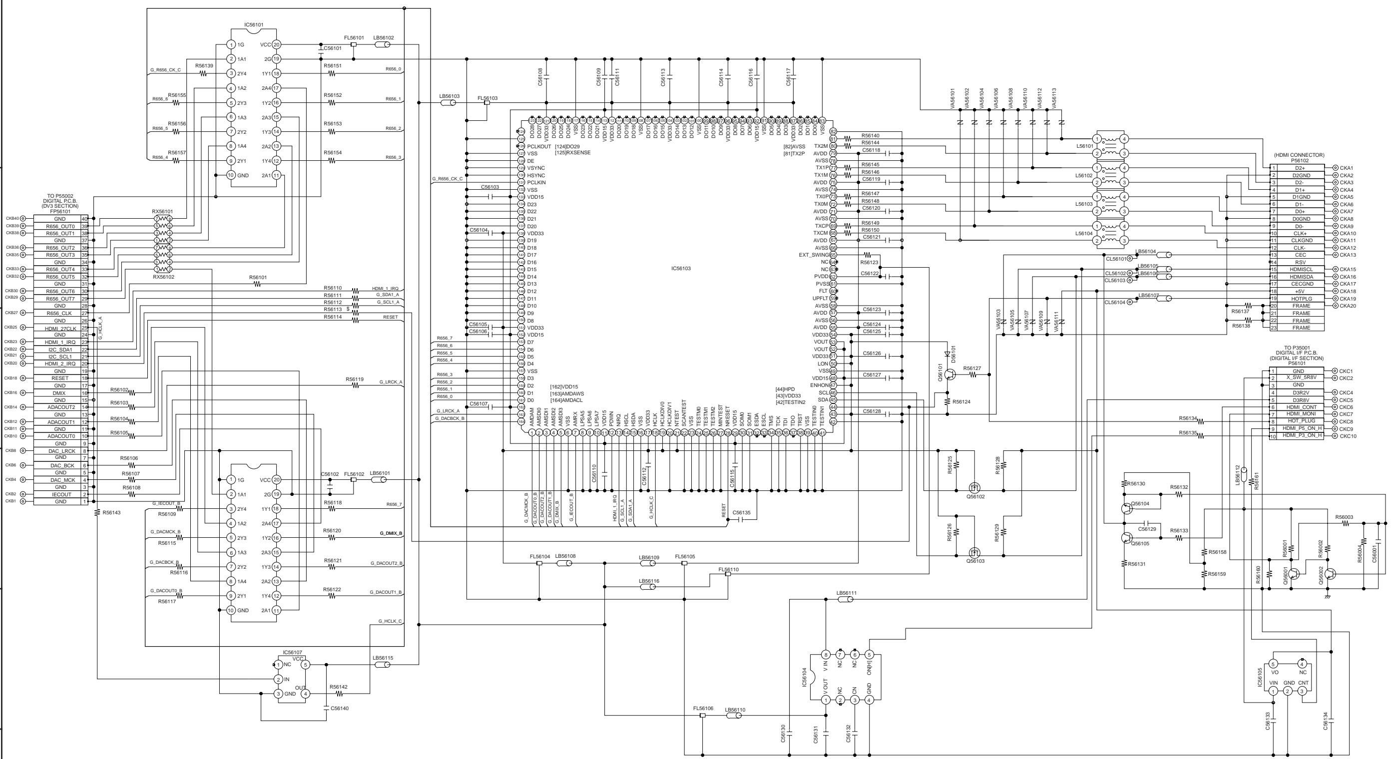
DMR-EX75EG/EC/EB
DMR-EX85EG/EB
HDMI
SCHEMATIC DIAGRAM
14 PRINTED CIRCUIT BOARD
14.1. POWER P.C.B.
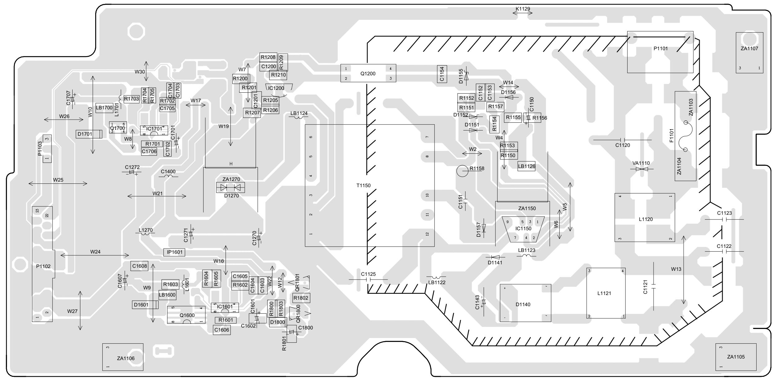
DMR-EX75EG
DMR-EX75EB
DMR-EX75EC
DMR-EX85EG
DMR-EX85EB
POWER
VEP71110A
14.2. MAIN P.C.B.
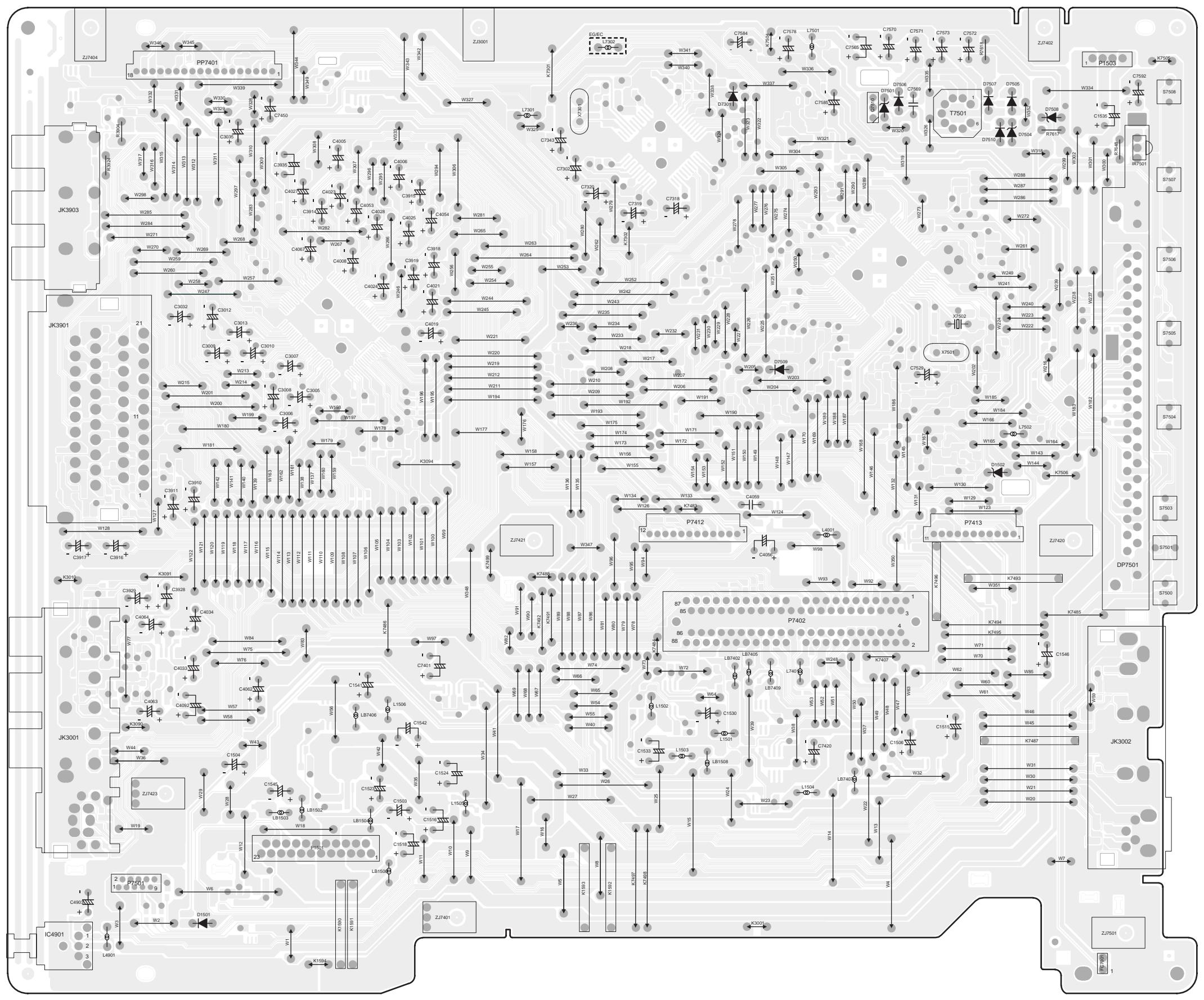
| ADRESS INFORMATION | |||
| DP7501 | D9 | PP7401 | G2 |
| FC7001 | A9 | Q7510 | G7 |
| IC4901 | A1 | T7501 | F7 |
| JK3001 | B1 | X7301 | G5 |
| JK3002 | B9 | X7501 | E7 |
| JK3901 | E1 | X7502 | E8 |
| JK3903 | F1 | ||
| P1501 | B3 | ||
| P1503 | G8 | ||
| P7402 | C6 | ||
| P7412 | D6 | ||
| P7413 | D8 | ||
| P7501 | A2 | ||
DMR-EX75EG/EC/EB
DMR-EX85EG/EB
MAIN PCB
COMPONENT SIDE
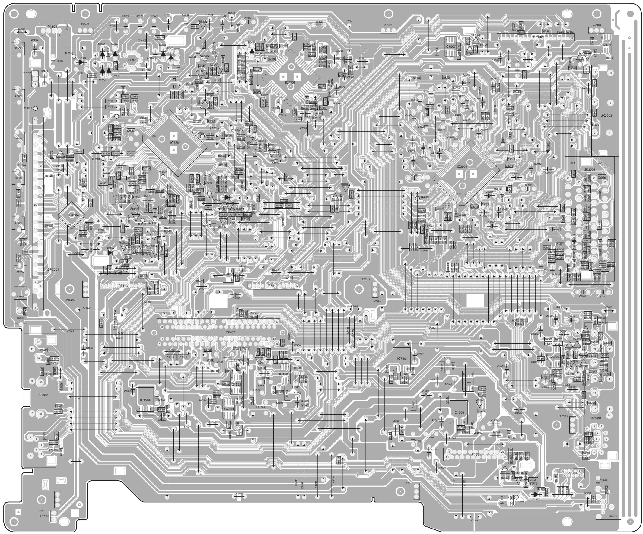
| ADRESS INFORMATION | |||||
| DP7501 | D1 | P1501 | B7 | QR4002 | E5 |
| P1503 | G1 | QR7401 | F3 | ||
| FC7001 | A1 | P7402 | C4 | QR7402 | G7 |
| P7412 | D4 | QR7403 | G7 | ||
| IC1504 | B3 | P7413 | D2 | QR7501 | E3 |
| IC1506 | B7 | P7501 | A8 | QR7502 | E3 |
| IC1508 | C4 | QR7503 | D4 | ||
| IC1520 | B4 | PP7401 | G8 | QR7504 | E4 |
| IC1521 | C4 | QR7506 | F4 | ||
| IC1522 | A7 | Q1501 | D2 | QR7507 | F3 |
| IC3001 | E7 | Q1502 | C7 | QR7508 | G3 |
| IC4009 | C8 | Q4006 | C8 | ||
| IC4011 | D4 | Q4007 | C9 | T7501 | F2 |
| IC4901 | A9 | Q4008 | C8 | ||
| IC7301 | F5 | Q4009 | C8 | TL3001 | E6 |
| IC7401 | C6 | Q4060 | E5 | TL7304 | F4 |
| IC7403 | G9 | Q7501 | D3 | TL7501 | E2 |
| IC7404 | B4 | Q7502 | D3 | TL7502 | F2 |
| IC7405 | D3 | Q7503 | D3 | TL7505 | E3 |
| IC7501 | F3 | Q7504 | D2 | TL7510 | A8 |
| IC7502 | E2 | Q7505 | A8 | TL7512 | F3 |
| IC7504 | E2 | Q7509 | G3 | TL7513 | F1 |
| IC7505 | G4 | Q7510 | F3 | TL7514 | G2 |
| IC7507 | G7 | Q7511 | A7 | TL7515 | E3 |
| Q7514 | E2 | TL7516 | E3 | ||
| IP1501 | B7 | Q7515 | F4 | TL7517 | E4 |
| IP7501 | G3 | Q7516 | F4 | TL7518 | E4 |
| Q7517 | E4 | TL7519 | E3 | ||
| JK3001 | B9 | TL7520 | E2 | ||
| JK3002 | B1 | QR1501 | B7 | ||
| JK3901 | E9 | QR1502 | C4 | X7301 | G5 |
| JK3903 | F9 | QR3901 | G8 | X7501 | E2 |
| QR3902 | G8 | X7502 | E3 | ||
DMR-EX75EG/EC/EB
DMR-EX85EG/EB
MAIN PCB
SOLDER SIDE
14.3. TUNER P.C.B. (REPD0032B)
COMPONENT SIDE
| ADDRESS INFORMATION | |
| CN7800 | G5 |
| TU7800 | E5 |
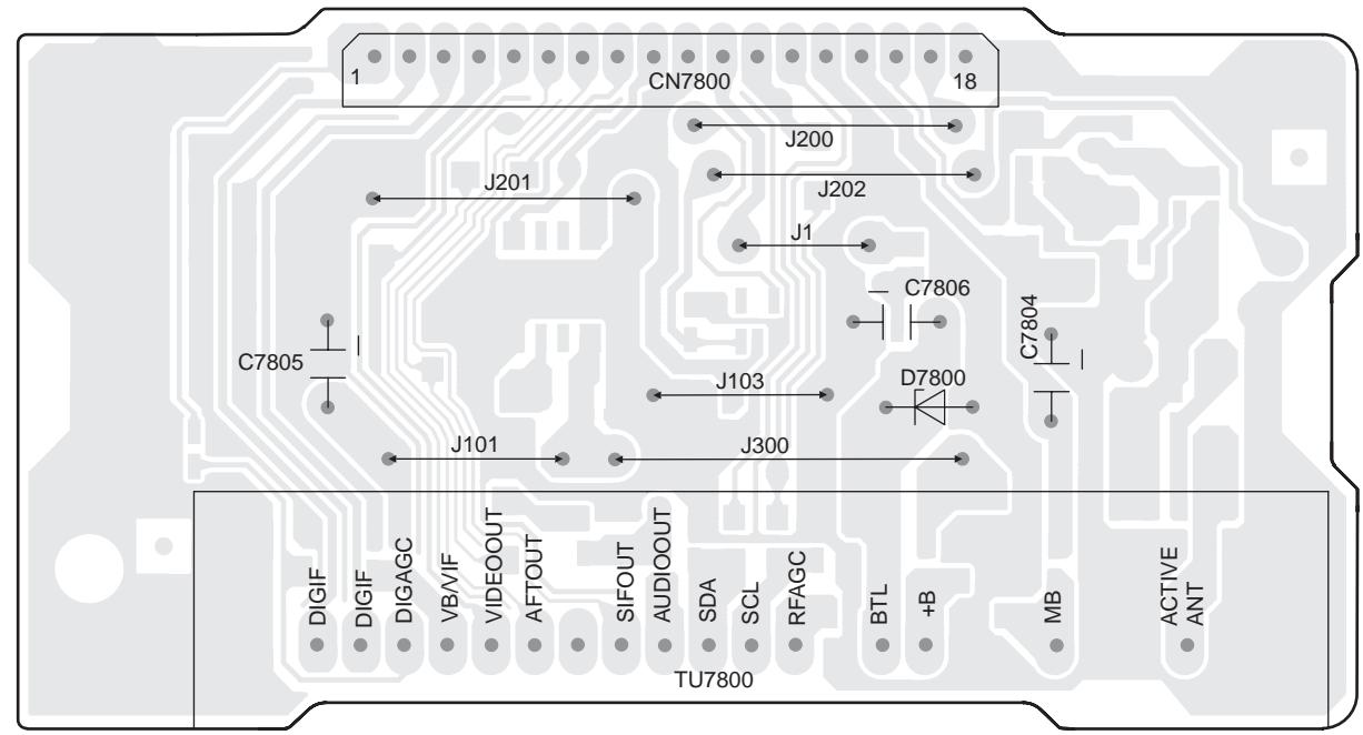
SOLDER SIDE
| ADDRESS INFORMATION | |
| IC7801 | C6 |
| CN7800 | D5 |
| TU7800 | B5 |
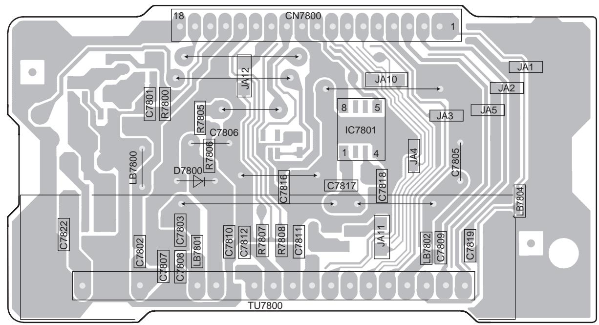
DMR-EX75EB
DMR-EX85EB
TUNER P.C.B.
REPD0032B
Circuit voltage and waveform described, shall be regarded as reference information when probing defect point, because it may differ from an actual measuring value due to difference of Measuring instrument and its measuring condition and product itself.
15.1.1. VOLTAGE CHART
15.1.1.1. POWER P.C.B.
| Ref No.MODE | IC1150 | IC1200 | ||||||||||||||||||
| 1 | 2 | 3 | 4 | 5 | 6 | 7 | 8 | 9 | 1 | 2 | 3 | |||||||||
| REC | 3.0 | 1.5 | 0 | 11.6 | 0 | - | 310 | - | -1523 | 8.3 | 2.5 | 0 | ||||||||
| PLAY | 3.0 | 1.5 | 0 | 11.6 | 0 | - | 310 | - | -1523 | 8.3 | 2.5 | 0 | ||||||||
| STOP | 3.0 | 1.5 | 0 | 11.6 | 0 | - | 310 | - | -1538 | 8.3 | 2.5 | 0 | ||||||||
| Ref No.MODE | IC1601 | IC1701 | ||||||||||||||||||
| 1 | 2 | 3 | 4 | 5 | 6 | 7 | 8 | 1 | 2 | 3 | 4 | 5 | 6 | 7 | 8 | |||||
| REC | 12.3 | 4.5 | 1.2 | 1.3 | 0.8 | 0 | 7.6 | 12.3 | 12.4 | 4.5 | 1.2 | 1.3 | 0 | 0 | 8.5 | 12.4 | ||||
| PLAY | 12.3 | 4.5 | 1.2 | 1.3 | 0.8 | 0 | 7.6 | 12.3 | 12.4 | 4.5 | 1.2 | 1.3 | 0 | 0 | 8.5 | 12.4 | ||||
| STOP | 12.3 | 4.5 | 1.2 | 1.3 | 0.8 | 0 | 7.6 | 12.3 | 12.4 | 4.5 | 1.2 | 1.3 | 1.2 | 0 | 8.5 | 12.4 | ||||
| Ref No.MODE | Q1200 | Q1600 | ||||||||||||||||||
| 1 | 2 | 3 | 4 | 1 | 2 | 3 | 4 | 5 | 6 | 7 | 8 | |||||||||
| REC | 9.3 | 8.3 | 0 | 1.5 | 12.3 | 12.3 | 12.3 | 7.6 | 6.1 | 6.1 | 6.1 | 6.1 | ||||||||
| PLAY | 9.3 | 8.3 | 0 | 1.5 | 12.3 | 12.3 | 12.3 | 7.6 | 6.1 | 6.1 | 6.1 | 6.1 | ||||||||
| STOP | 9.3 | 8.3 | 0 | 1.5 | 12.3 | 12.3 | 12.3 | 7.6 | 6.1 | 6.1 | 6.1 | 6.1 | ||||||||
| Ref No.MODE | QR1800 | QR1801 | ||||||||||||||||||
| E | C | B | E | C | B | |||||||||||||||
| REC | 11.9 | 0 | 12.3 | 0 | 4.5 | 0 | ||||||||||||||
| PLAY | 11.9 | 0 | 12.3 | 0 | 4.5 | 0 | ||||||||||||||
| STOP | 11.9 | 0 | 12.3 | 0 | 4.5 | 0 | ||||||||||||||
15.1.1.2. MAIN P.C.B. - PART 1
| Ref No. MODE | IC1505 | IC1506 | ||||||||||||||||||
| 1 | 2 | 3 | 4 | 5 | 1 | 2 | 3 | 4 | 5 | |||||||||||
| REC | 4.1 | 0 | 4.9 | - | 3.3 | 4.8 | 6.1 | 0 | 5.2 | 5.2 | ||||||||||
| PLAY | 4.1 | 0 | 4.9 | - | 3.3 | 4.8 | 6.1 | 0 | 5.2 | 5.2 | ||||||||||
| STOP | 4.1 | 0 | 4.9 | - | 3.3 | 4.8 | 6.1 | 0 | 5.2 | 5.2 | ||||||||||
| Ref No. MODE | IC1507 | IC1510 | IC1520 | |||||||||||||||||
| 1 | 2 | 3 | 4 | 5 | 6 | 7 | 8 | 1 | 2 | 3 | 4 | 5 | 1 | 2 | 3 | 4 | 5 | |||
| REC | 5.1 | - | 3.4 | 0 | 6.1 | - | - | 6.1 | 6.1 | 4.9 | 5.0 | - | 0 | 6.1 | 0 | 4.8 | - | 5.1 | ||
| PLAY | 5.1 | - | 3.4 | 0 | 6.1 | - | - | 6.1 | 6.1 | 4.9 | 5.0 | - | 0 | 6.1 | 0 | 4.8 | - | 5.1 | ||
| STOP | 5.1 | - | 3.4 | 0 | 6.1 | - | - | 6.1 | 6.1 | 4.9 | 5.0 | - | 0 | 6.1 | 0 | 4.8 | - | 5.1 | ||
| Ref No. MODE | IC1521 | IC1522 | ||||||||||||||||||
| 1 | 2 | 3 | 4 | 5 | 6 | 7 | 8 | 1 | 2 | 3 | 4 | 5 | ||||||||
| REC | 3.3 | - | 2.0 | 0 | 4.8 | - | - | 4.1 | - | 0 | 0 | 5.0 | 5.1 | |||||||
| PLAY | 3.3 | - | 2.0 | 0 | 4.8 | - | - | 4.1 | - | 0 | 0 | 5.0 | 5.1 | |||||||
| STOP | 3.3 | - | 2.0 | 0 | 4.8 | - | - | 4.1 | - | 0 | 0 | 5.0 | 5.1 | |||||||
| Ref No. MODE | IC3001 | |||||||||||||||||||
| 1 | 2 | 3 | 4 | 5 | 6 | 7 | 8 | 9 | 10 | 11 | 12 | 13 | 14 | 15 | 16 | 17 | 18 | 19 | 20 | |
| REC | 2.0 | 2.5 | 1.6 | 0 | 1.6 | 5.0 | 1.6 | 5.0 | 0.4 | 0.3 | 1.6 | 0.4 | - | 1.7 | 1.7 | 1.6 | 0.4 | 0 | 1.7 | 1.7 |
| PLAY | 2.0 | 2.5 | 1.6 | 0 | 1.6 | 5.0 | 1.6 | 5.0 | 0.4 | 0.3 | 1.6 | 0.4 | - | 1.7 | 1.7 | 1.6 | 0.4 | 0 | 1.7 | 1.7 |
| STOP | 2.0 | 2.5 | 1.6 | 0 | 1.6 | 5.0 | 1.6 | 5.0 | 0.4 | 1.6 | 1.6 | 0.4 | - | 1.7 | 1.7 | 1.6 | 0.4 | 0 | 1.7 | 1.7 |
| Ref No. MODE | IC3001 | |||||||||||||||||||
| 21 | 22 | 23 | 24 | 25 | 26 | 27 | 28 | 29 | 30 | 31 | 32 | 33 | 34 | 35 | 36 | 37 | 38 | 39 | 40 | |
| REC | 0 | 1.7 | 1.7 | 1.7 | 5.0 | 1.4 | 0.1 | 1.4 | 0 | 2.1 | 1.6 | 0 | 1.6 | 0 | 2.1 | - | 1.6 | - | 1.6 | 5.0 |
| PLAY | 0 | 1.7 | 1.7 | 1.7 | 5.0 | 1.4 | 0.1 | 1.4 | 0 | 2.1 | 1.6 | 0 | 1.6 | 0 | 2.1 | - | 1.6 | - | 1.6 | 5.0 |
| STOP | 0 | 1.7 | 1.6 | 1.7 | 5.0 | 1.4 | 0.2 | 1.4 | 0 | 2.1 | 1.6 | 0 | 1.6 | 0 | 2.1 | - | 1.6 | - | 1.6 | 5.0 |
| Ref No. MODE | IC3001 | |||||||||||||||||||
| 41 | 42 | 43 | 44 | 45 | 46 | 47 | 48 | 49 | 50 | 51 | 52 | 53 | 54 | 55 | 56 | 57 | 58 | 59 | 60 | |
| REC | 1.6 | 5.1 | 2.0 | 0 | 2.0 | 11.6 | 1.6 | 2.0 | 4.5 | 4.4 | 4.4 | 4.0 | 4.5 | 4.5 | - | 4.5 | 9.1 | 4.4 | 4.4 | 4.5 |
| PLAY | 1.6 | 5.1 | 2.0 | 0 | 2.0 | 11.6 | 1.6 | 2.0 | 4.5 | 4.4 | 4.4 | 4.0 | 4.5 | 4.5 | - | 4.5 | 9.1 | 4.4 | 4.4 | 4.5 |
| STOP | 1.6 | 5.1 | 2.0 | 0 | 2.0 | 11.6 | 1.6 | 2.0 | 4.5 | 4.5 | 4.0 | 4.5 | 4.5 | 4.4 | - | 3.9 | 9.1 | 4.0 | 4.3 | 3.7 |
| Ref No. MODE | IC3001 | |||||||||||||||||||
| 61 | 62 | 63 | 64 | 65 | 66 | 67 | 68 | 69 | 70 | 71 | 72 | 73 | 74 | 75 | 76 | 77 | 78 | 79 | 80 | |
| REC | 4.5 | 4.5 | - | 4.5 | 9.0 | 0 | 0 | 0 | 0 | 0 | 4.5 | 4.5 | 4.5 | 4.5 | 0 | - | 9.5 | 4.5 | 4.5 | 0 |
| PLAY | 4.5 | 4.5 | - | 4.5 | 9.0 | 0 | 0 | 0 | 0 | 0 | 4.5 | 4.5 | 4.5 | 4.5 | 0 | - | 9.5 | 4.5 | 4.5 | 0 |
| STOP | 3.7 | 3.7 | - | 3.8 | 9.0 | 0 | 0 | 0 | 0 | 0 | 4.5 | 4.5 | 4.5 | 4.5 | 0 | - | 0.3 | 4.5 | 4.5 | 0 |
| Ref No. MODE | IC3001 | |||||||||||||||||||
| 81 | 82 | 83 | 84 | 85 | 86 | 87 | 88 | 89 | 90 | 91 | 92 | 93 | 94 | 95 | 96 | 97 | 98 | 99 | 100 | |
| REC | 2.1 | 5.0 | 1.5 | 5.1 | 2.1 | 4.5 | 3.6 | 4.8 | 4.6 | 5.0 | 2.0 | 2.8 | 2.1 | 5.1 | 2.0 | 0 | 2.1 | 0 | 2.0 | 2.5 |
| PLAY | 2.1 | 5.0 | 1.5 | 5.1 | 2.1 | 4.5 | 3.6 | 4.8 | 4.6 | 5.0 | 2.0 | 2.8 | 2.1 | 5.1 | 2.0 | 0 | 2.1 | 0 | 2.0 | 2.5 |
| STOP | 4.7 | 5.0 | 1.5 | 5.1 | 2.1 | 4.5 | 3.6 | 4.8 | 4.6 | 5.1 | 5.0 | 2.8 | 2.1 | 5.1 | 2.0 | 0 | 2.1 | 0 | 2.0 | 2.5 |
15.1.1.3. MAIN P.C.B. - PART 2
| Ref No. | IC4009 | IC4011 | ||||||||||||||||||
| MODE | 1 | 2 | 3 | 4 | 5 | 6 | 7 | 8 | 1 | 2 | 3 | 4 | 5 | |||||||
| REC | 5.8 | 5.8 | 5.8 | 0 | 5.8 | 5.8 | 5.8 | 11.6 | 3.4 | 0 | 4.8 | 6.1 | 5.0 | |||||||
| PLAY | 5.8 | 5.8 | 5.8 | 0 | 5.8 | 5.8 | 5.8 | 11.6 | 3.4 | 0 | 4.8 | 6.1 | 5.0 | |||||||
| STOP | 5.8 | 5.8 | 5.8 | 0 | 5.8 | 5.8 | 5.8 | 11.6 | 3.4 | 0 | 4.8 | 6.1 | 5.0 | |||||||
| Ref No. | IC4012 | IC4901 | ||||||||||||||||||
| MODE | 1 | 2 | 3 | 4 | 5 | 6 | 7 | 8 | 1 | 2 | 3 | |||||||||
| REC | 5.8 | 5.8 | 5.8 | 0 | 5.8 | 5.8 | 5.8 | 11.6 | 1.7 | 5.0 | 0 | |||||||||
| PLAY | 5.8 | 5.8 | 5.8 | 0 | 5.8 | 5.8 | 5.8 | 11.6 | 1.7 | 5.0 | 0 | |||||||||
| STOP | 5.8 | 5.8 | 5.8 | 0 | 5.8 | 5.8 | 5.8 | 11.6 | 1.7 | 5.0 | 0 | |||||||||
| Ref No. | IC7301 | |||||||||||||||||||
| MODE | 1 | 2 | 3 | 4 | 5 | 6 | 7 | 8 | 9 | 10 | 11 | 12 | 13 | 14 | 15 | 16 | 17 | 18 | 19 | 20 |
| REC | 2.4 | 2.4 | 2.4 | 0 | 0 | 2.4 | 0 | 2.4 | 0 | 2.4 | 0 | - | 0 | 2.9 | 2.6 | 0 | 0 | 2.8 | 0 | 0 |
| PLAY | 2.4 | 2.4 | 2.4 | 0 | 0 | 2.4 | 0 | 2.4 | 0 | 2.4 | 0 | - | 0 | 2.9 | 2.6 | 0 | 0 | 2.8 | 0 | 0 |
| STOP | 2.4 | 2.4 | 2.4 | 0 | 0 | 2.4 | 0 | 2.4 | 0 | 2.4 | 0 | - | 0 | 2.9 | 2.6 | 0 | 0 | 2.8 | 0 | 0 |
| Ref No. | IC7301 | |||||||||||||||||||
| MODE | 21 | 22 | 23 | 24 | 25 | 26 | 27 | 28 | 29 | 30 | 31 | 32 | 33 | 34 | 35 | 36 | 37 | 38 | 39 | 40 |
| REC | 2.3 | 0 | - | 1.5 | 2.4 | 1.4 | 0 | 5.0 | 5.0 | 5.0 | 2.9 | 2.4 | 2.4 | 2.5 | 2.5 | 0 | - | 2.4 | - | - |
| PLAY | 2.3 | 0 | - | 1.5 | 2.4 | 1.4 | 0 | 5.0 | 5.0 | 5.0 | 2.9 | 2.4 | 2.4 | 2.5 | 2.5 | 0 | - | 2.4 | - | - |
| STOP | 2.3 | 0 | - | 1.5 | 2.4 | 1.4 | 0 | 5.0 | 5.0 | 5.0 | 2.9 | 2.4 | 2.4 | 2.5 | 2.5 | 0 | - | 2.4 | - | - |
| Ref No. | IC7301 | |||||||||||||||||||
| MODE | 41 | 42 | 43 | 44 | ||||||||||||||||
| REC | 2.4 | - | - | 0 | ||||||||||||||||
| PLAY | 2.4 | - | - | 0 | ||||||||||||||||
| STOP | 2.4 | - | - | 0 | ||||||||||||||||
| Ref No. | IC7302 | IC7401 | IC7402 | |||||||||||||||||
| MODE | 1 | 2 | 3 | 1 | 2 | 3 | 4 | 5 | 1 | 2 | 3 | 4 | 5 | |||||||
| REC | 5.0 | 0 | 4.9 | 12.4 | 4.2 | 11.6 | 2.6 | 0 | 6.1 | 0 | 6.1 | - | 5.1 | |||||||
| PLAY | 5.0 | 0 | 4.9 | 12.4 | 4.2 | 11.6 | 2.6 | 0 | 6.1 | 0 | 6.1 | - | 5.1 | |||||||
| STOP | 5.0 | 0 | 4.9 | 12.4 | 4.2 | 11.6 | 2.6 | 0 | 6.1 | 0 | 6.1 | - | 5.1 | |||||||
| Ref No. | IC7403 | IC7404 | ||||||||||||||||||
| MODE | 1 | 2 | 3 | 4 | 5 | 6 | 7 | 8 | 1 | 2 | 3 | 4 | 5 | 6 | 7 | 8 | ||||
| REC | 5.0 | - | 3.4 | 0 | 4.2 | - | - | 6.1 | 0 | 0 | 0 | 0 | 3.2 | 3.2 | 0 | 3.3 | ||||
| PLAY | 5.0 | - | 3.4 | 0 | 4.2 | - | - | 6.1 | 0 | 0 | 0 | 0 | 3.2 | 3.2 | 0 | 3.3 | ||||
| STOP | 5.0 | - | 3.4 | 0 | 4.2 | - | - | 6.1 | 0 | 0 | 0 | 0 | 3.2 | 3.2 | 0 | 3.3 | ||||
| Ref No. | IC7501 | |||||||||||||||||||
| MODE | 1 | 2 | 3 | 4 | 5 | 6 | 7 | 8 | 9 | 10 | 11 | 12 | 13 | 14 | 15 | 16 | 17 | 18 | 19 | 20 |
| REC | 0.3 | - | 4.9 | 3.8 | 0.8 | 0.8 | 4.4 | 0 | 0 | 2.1 | 1.2 | 4.9 | 1.4 | 0 | 2.1 | 3.3 | 4.9 | 3.3 | 3.2 | - |
| PLAY | 0.3 | - | 4.9 | 3.8 | 0.8 | 0.8 | 4.4 | 0 | 0 | 0.7 | 1.2 | 4.9 | 1.4 | 0 | 2.1 | 3.3 | 4.9 | 3.3 | 3.2 | - |
| STOP | 0.3 | - | 4.9 | 4.5 | 0.9 | 0.9 | 4.4 | 0 | 0 | 0.7 | 1.2 | 4.9 | 1.4 | 0 | 2.1 | 3.3 | 4.9 | 3.3 | 3.2 | - |
| Ref No. | IC7501 | |||||||||||||||||||
| MODE | 21 | 22 | 23 | 24 | 25 | 26 | 27 | 28 | 29 | 30 | 31 | 32 | 33 | 34 | 35 | 36 | 37 | 38 | 39 | 40 |
| REC | 3.1 | - | 3.2 | 0 | - | - | - | - | 4.8 | 4.6 | 3.3 | 3.3 | 0 | - | 3.3 | 3.2 | 3.3 | - | 0 | 4.9 |
| PLAY | 3.1 | - | 3.2 | 0 | - | - | - | - | 4.8 | 4.6 | 3.3 | 3.3 | 0 | - | 3.3 | 3.2 | 3.3 | - | 0 | 4.9 |
| STOP | 3.1 | - | 3.2 | 0 | - | - | - | - | 4.8 | 4.6 | 3.3 | 3.3 | 0 | - | 3.3 | 3.2 | 3.3 | - | 0 | 4.9 |
| Ref No. | IC7501 | |||||||||||||||||||
| MODE | 41 | 42 | 43 | 44 | 45 | 46 | 47 | 48 | 49 | 50 | 51 | 52 | 53 | 54 | 55 | 56 | 57 | 58 | 59 | 60 |
| REC | 0 | 4.9 | 4.9 | 4.8 | 0 | 4.9 | 5.0 | 5.0 | 4.9 | 0 | 4.9 | - | 0 | - | -0.1 | 0 | 0 | 0 | - | 5.0 |
| PLAY | 0 | 4.9 | 4.9 | 4.8 | 0 | 4.9 | 5.0 | 5.0 | 4.9 | 0 | 4.9 | - | 0 | - | -0.1 | 0 | 0 | 0 | - | 5.0 |
| STOP | 4.9 | 4.9 | 4.9 | 4.8 | 0 | 4.9 | 5.0 | 5.0 | 4.9 | 0 | 4.9 | - | 0 | - | -0.1 | 0 | 0 | 0 | - | 5.0 |
| Ref No. | IC7501 | |||||||||||||||||||
| MODE | 61 | 62 | 63 | 64 | 65 | 66 | 67 | 68 | 69 | 70 | 71 | 72 | 73 | 74 | 75 | 76 | 77 | 78 | 79 | 80 |
| REC | 0 | 5.0 | 0 | 0 | 4.9 | - | - | - | - | - | - | - | 4.9 | 0 | 5.0 | 0 | - | - | 0 | - |
| PLAY | 0 | 5.0 | 0 | 0 | 4.9 | - | - | - | - | - | - | - | 4.9 | 0 | 5.0 | 0 | - | - | 0 | - |
| STOP | 0 | 5.0 | 0 | 0 | 4.9 | - | - | - | - | - | - | - | 4.9 | 0 | 5.0 | 0 | - | - | 0 | - |
| Ref No. | IC7501 | |||||||||||||||||||
| MODE | 81 | 82 | 83 | 84 | 85 | 86 | 87 | 88 | 89 | 90 | 91 | 92 | 93 | 94 | 95 | 96 | 97 | 98 | 99 | 100 |
| REC | 3.3 | 0 | 0 | 4.7 | 3.2 | 5.0 | 5.0 | 5.0 | 2.0 | 5.0 | 0 | 0 | 2.5 | 1.2 | 1.6 | 0 | 0 | 2.0 | 5.0 | 0 |
| PLAY | 3.3 | 0 | 0 | 4.7 | 3.2 | 5.0 | 5.0 | 5.0 | 2.0 | 5.0 | 0 | 0 | 2.5 | 1.2 | 1.6 | 0 | 0 | 2.0 | 5.0 | 0 |
| STOP | 3.3 | 0 | 0 | 4.7 | 0 | 5.0 | 5.0 | 5.0 | 2.0 | 5.0 | 0 | 0 | 2.5 | 1.2 | 1.6 | 0 | 0 | 2.0 | 5.0 | 0 |
| Ref No. | IC7502 | |||||||||||||||||||
| MODE | 1 | 2 | 3 | 4 | 5 | |||||||||||||||
| REC | 0 | 0 | - | 4.9 | 5.0 | |||||||||||||||
| PLAY | 0 | 0 | - | 4.9 | 5.0 | |||||||||||||||
| STOP | 0 | 0 | - | 4.9 | 5.0 | |||||||||||||||
| Ref No. | IC7504 | |||||||||||||||||||
| MODE | 1 | 2 | 3 | 4 | 5 | 6 | 7 | 8 | 9 | 10 | 11 | 12 | 13 | 14 | 15 | 16 | 17 | 18 | 19 | 20 |
| REC | - | - | 0 | 0 | 2.2 | 2.2 | 5.0 | 4.9 | 4.4 | 2.5 | -18.1 | -21.1 | -21.1 | - | -21.8 | -21.1 | - | -17.6 | -17.6 | -18.1 |
| PLAY | - | - | 0 | 0 | 2.2 | 2.2 | 5.0 | 4.9 | 4.4 | 2.5 | -18.1 | -17.6 | -17.6 | - | -21.8 | -17.6 | - | -21.1 | -21.1 | -18.1 |
| STOP | - | - | 0 | 0 | 2.2 | 2.2 | 5.0 | 4.9 | 4.4 | 0.8 | -18.1 | -21.1 | -21.1 | - | -21.8 | -21.1 | - | -17.6 | -17.6 | -18.1 |
| Ref No. | IC7504 | |||||||||||||||||||
| MODE | 21 | 22 | 23 | 24 | 25 | 26 | 27 | 28 | 29 | 30 | 31 | 32 | 33 | 34 | 35 | 36 | 37 | 38 | 39 | 40 |
| REC | -17.6 | -14.2 | -18.1 | -14.2 | -21.0 | -17.7 | -21.0 | -10.8 | -17.7 | -17.6 | -17.6 | -17.6 | -17.7 | -17.6 | -17.7 | -17.9 | -17.9 | - | - | - |
| PLAY | -17.6 | -0.6 | -18.1 | -4.0 | -14.3 | -17.7 | -10.8 | -4.0 | -17.7 | -10.8 | -21.1 | -21.1 | -17.7 | -21.4 | -17.7 | -4.4 | -4.4 | - | - | - |
| STOP | -17.6 | -14.2 | -18.1 | -14.2 | -21.0 | -17.7 | -21.0 | -10.8 | -17.7 | -17.6 | -17.6 | -17.6 | -17.7 | -17.6 | -17.7 | -17.9 | -19.9 | - | - | - |
15.1.1.4. MAIN P.C.B. - PART 3
| Ref No. MODE | Q1501 | Q1509 | |||||||||||||||||
| 1 | 2 | 3 | 4 | 5 | 6 | 7 | 8 | 1 | 2 | 3 | 4 | 5 | 6 | 7 | 8 | ||||
| REC | 5.2 | 5.2 | 5.2 | 0.6 | 5.1 | 5.1 | 5.1 | 5.1 | 12.4 | 12.4 | 12.4 | 6.2 | 12.3 | 12.3 | 12.3 | 12.3 | |||
| PLAY | 5.2 | 5.2 | 5.2 | 0.6 | 5.1 | 5.1 | 5.1 | 5.1 | 12.4 | 12.4 | 12.4 | 6.2 | 12.3 | 12.3 | 12.3 | 12.3 | |||
| STOP | 5.2 | 5.2 | 5.2 | 0.6 | 5.1 | 5.1 | 5.1 | 5.1 | 12.4 | 12.4 | 12.4 | 6.2 | 12.3 | 12.3 | 12.3 | 12.3 | |||
| Ref No. MODE | Q4006 | Q4007 | Q4008 | Q4009 | Q7401 | ||||||||||||||
| E | C | B | E | C | B | E | C | B | E | C | B | E | C | B | |||||
| REC | 0 | 0 | -0.1 | 0 | 0 | -0.1 | 0 | 0 | -0.1 | 0 | 0 | -0.1 | 0 | 11.6 | 0 | ||||
| PLAY | 0 | 0 | -0.1 | 0 | 0 | -0.1 | 0 | 0 | -0.1 | 0 | 0 | -0.1 | 0 | 11.6 | 0 | ||||
| STOP | 0 | 0 | -0.1 | 0 | 0 | -0.1 | 0 | 0 | -0.1 | 0 | 0 | -0.1 | 0 | 11.6 | 0 | ||||
| Ref No. MODE | Q7402 | Q7501 | Q7502 | Q7503 | Q7504 | ||||||||||||||
| E | C | B | E | C | B | E | C | B | E | C | B | E | C | B | |||||
| REC | 0 | 0 | 4.9 | 2.7 | 0 | 2.1 | 2.0 | 5.0 | 1.6 | 2.7 | 0 | 2.1 | 2.0 | 5.0 | 1.6 | ||||
| PLAY | 0 | 0 | 4.9 | 2.7 | 0 | 2.1 | 2.0 | 5.0 | 1.6 | 2.7 | 0 | 2.1 | 2.0 | 5.0 | 1.6 | ||||
| STOP | 0 | 0 | 4.9 | 2.7 | 0 | 2.1 | 2.0 | 5.0 | 1.6 | 2.7 | 0 | 2.1 | 2.0 | 5.0 | 1.6 | ||||
| Ref No. MODE | Q7505 | Q7506 | Q7507 | Q7508 | Q7510 | ||||||||||||||
| E | C | B | E | C | B | E | C | B | E | C | B | E | C | B | |||||
| REC | -18.1 | 5.0 | -18.0 | 0 | 5.0 | 0 | 0 | 0 | 4.6 | 0 | 4.6 | 0 | 0 | 9.1 | -0.2 | ||||
| PLAY | -18.1 | 5.0 | -18.0 | 0 | 5.0 | 0 | 0 | 0 | 4.6 | 0 | 4.6 | 0 | 0 | 9.3 | -0.1 | ||||
| STOP | -18.1 | 5.0 | -18.0 | 0 | 5.0 | 0 | 0 | 0 | 5.1 | 0 | 5.1 | 0.1 | 0 | 9.1 | -0.2 | ||||
| Ref No. MODE | Q7511 | ||||||||||||||||||
| E | C | B | |||||||||||||||||
| REC | 5.1 | 12.3 | 5.5 | ||||||||||||||||
| PLAY | 5.1 | 12.3 | 5.5 | ||||||||||||||||
| STOP | 5.1 | 12.3 | 5.5 | ||||||||||||||||
| Ref No. MODE | QR1501 | QR1503 | QR4002 | QR4003 | QR4004 | ||||||||||||||
| E | C | B | E | C | B | E | C | B | E | C | B | E | C | B | |||||
| REC | 0 | 0 | 4.9 | 0 | 0 | 4.9 | 5.1 | -0.1 | 5.1 | 0 | 0 | 2.3 | 0 | 5.1 | 0 | ||||
| PLAY | 0 | 0 | 4.9 | 0 | 0 | 4.9 | 5.1 | -0.1 | 5.1 | 0 | 0 | 2.3 | 0 | 5.1 | 0 | ||||
| STOP | 0 | 0 | 4.9 | 0 | 0 | 4.9 | 5.1 | -0.1 | 5.1 | 0 | 0 | 2.3 | 0 | 5.1 | 0 | ||||
| Ref No. MODE | QR7401 | QR7402 | QR7403 | QR7404 | |||||||||||||||
| E | C | B | E | C | B | E | C | B | E | C | B | ||||||||
| REC | 0 | 4.2 | 0 | 38.1 | 38.0 | 0 | 0 | 0 | 4.9 | 0 | 0 | 0 | |||||||
| PLAY | 0 | 4.2 | 0 | 38.1 | 38.0 | 0 | 0 | 0 | 4.9 | 0 | 0 | 0 | |||||||
| STOP | 0 | 4.2 | 0 | 38.1 | 38.0 | 0 | 0 | 0 | 4.9 | 0 | 0 | 0 | |||||||
| Ref No. MODE | QR7507 | QR7508 | |||||||||||||||||
| E | C | B | E | C | B | ||||||||||||||
| REC | 0 | 0 | 4.9 | 0 | -0.2 | 0 | |||||||||||||
| PLAY | 0 | 0 | 4.9 | 0 | -0.1 | 0 | |||||||||||||
| STOP | 0 | 0 | 4.9 | 0 | -0.2 | 0 | |||||||||||||
15.1.1.5. TUNER P.C.B.
| Ref No.MODE | Q7802 | ||||||||||||||||||
| E | C | B | |||||||||||||||||
| REC | 3.8 | 1.2 | 3.1 | ||||||||||||||||
| PLAY | 3.8 | 1.2 | 3.1 | ||||||||||||||||
| STOP | 3.8 | 1.2 | 3.1 | ||||||||||||||||
15.1.1.6. P59001 CONNECTOR
| Ref No. MODE | P59001 | ||||||||||||||||||||
| 1 | 2 | 3 | 4 | 5 | 6 | 7 | 8 | 9 | 10 | 11 | 12 | 13 | 14 | 15 | 16 | 17 | 18 | 19 | 20 | ||
| REC | 0 | 0 | 0 | 0 | 0 | 0 | 0 | 0 | 0 | 0 | 0 | 0 | 3.3 | 12.3 | 4.9 | 12.3 | 3.3 | 0 | 4.9 | 0 | |
| PLAY | 0 | 0 | 0 | 0 | 0 | 0 | 0 | 0 | 0 | 0 | 0 | 0 | 3.3 | 12.3 | 4.9 | 12.3 | 3.3 | 0 | 4.9 | 0 | |
| STOP | 0 | 0 | 0 | 0 | 0 | 0 | 0 | 0 | 0 | 0 | 0 | 0 | 3.3 | 12.3 | 4.9 | 12.3 | 3.3 | 0 | 4.9 | 0 | |
| Ref No. MODE | P59001 | ||||||||||||||||||||
| 21 | 22 | 23 | 24 | 25 | 26 | 27 | 28 | 29 | 30 | 31 | 32 | 33 | 34 | 35 | 36 | 37 | 38 | 39 | 40 | ||
| REC | 3.3 | 5.1 | 3.3 | 5.1 | 5.0 | 3.3 | 2.3 | 3.1 | 2.5 | 4.9 | 2.5 | 3.3 | 0 | 3.3 | 0 | 3.3 | 0 | 3.3 | 2.5 | - | |
| PLAY | 3.3 | 5.1 | 3.3 | 5.1 | 5.0 | 3.3 | 2.3 | 3.1 | 2.5 | 4.9 | 2.5 | 3.3 | 0 | 3.3 | 0 | 3.3 | 0 | 3.3 | 2.5 | - | |
| STOP | 3.3 | 5.1 | 3.3 | 5.1 | 5.0 | 3.3 | 2.3 | 3.2 | 2.5 | 4.9 | 2.5 | 3.3 | 0 | 3.3 | 0 | 3.3 | 0 | 3.3 | 2.5 | - | |
| Ref No. MODE | P59001 | ||||||||||||||||||||
| 41 | 42 | 43 | 44 | 45 | 46 | 47 | 48 | 49 | 50 | 51 | 52 | 53 | 54 | 55 | 56 | 57 | 58 | 59 | 60 | ||
| REC | 2.5 | 3.2 | 0 | 1.7 | 0 | 0 | 0 | 3.3 | 0 | 3.3 | 1.1 | - | 0 | 0.3 | 1.5 | 3.3 | 0 | - | 1.0 | 4.8 | |
| PLAY | 2.5 | 3.2 | 0 | 1.7 | 0 | 0 | 0 | 3.3 | 0 | 3.3 | 1.1 | - | 0 | 0.3 | 1.5 | 3.3 | 0 | - | 1.0 | 4.8 | |
| STOP | 2.5 | 3.2 | 0 | 1.7 | 0 | 0 | 0 | 3.3 | 0 | 3.3 | 1.1 | - | 0 | 0.3 | 1.5 | 3.3 | 0 | - | 1.0 | 4.8 | |
| Ref No. MODE | P59001 | ||||||||||||||||||||
| 61 | 62 | 63 | 64 | 65 | 66 | 67 | 68 | 69 | 70 | 71 | 72 | 73 | 74 | 75 | 76 | 77 | 78 | 79 | 80 | ||
| REC | 0 | 4.8 | 1.1 | 12.3 | 0 | 12.3 | 1.0 | 12.3 | 0 | 12.3 | 1.3 | 12.3 | 0 | 12.3 | 2.1 | 5.0 | 0 | 0 | - | - | |
| PLAY | 0 | 4.8 | 1.1 | 12.3 | 0 | 12.3 | 1.0 | 12.3 | 0 | 12.3 | 1.3 | 12.3 | 0 | 12.3 | 2.1 | 5.0 | 0 | 0 | - | - | |
| STOP | 0 | 4.8 | 1.1 | 12.3 | 0 | 12.3 | 1.0 | 12.3 | 0 | 12.3 | 1.3 | 12.3 | 0 | 12.3 | 2.1 | 5.0 | 0 | 0 | - | - | |
| Ref No. MODE | P59001 | ||||||||||||||||||||
| 81 | 82 | 83 | 84 | 85 | 86 | 87 | 88 | ||||||||||||||
| REC | 0 | 0 | 0 | .33 | 0 | 0 | 0 | 0 | |||||||||||||
| PLAY | 0 | 0 | 0 | 0.3 | 0 | 0 | 0 | 0 | |||||||||||||
| STOP | 0 | 0 | 0 | 0.3 | 0 | 0 | 0 | 0 | |||||||||||||
15.1.2. WAVEFORM CHART
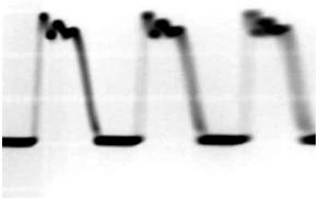 T1150-4,5 STOP30Vp-p (5 μ sec.div) T1150-4,5 STOP30Vp-p (5 μ sec.div) | 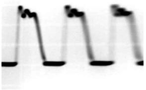 T1150-8 STOP30Vp-p (5 μ sec.div) T1150-8 STOP30Vp-p (5 μ sec.div) | 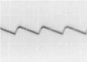 T1150-12 STOP10Vp-p (2m sec.div) T1150-12 STOP10Vp-p (2m sec.div) | 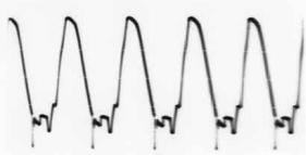 IC1150-1 STOP10.0Vp-p (5 μ sec.div) IC1150-1 STOP10.0Vp-p (5 μ sec.div) |
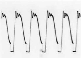 IC1150-9 STOP580Vp-p (5 μ sec.div) IC1150-9 STOP580Vp-p (5 μ sec.div) | 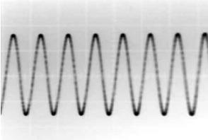 P7402-29,31 REC/PLAY0.8Vp-p (1m sec.div) P7402-29,31 REC/PLAY0.8Vp-p (1m sec.div) | 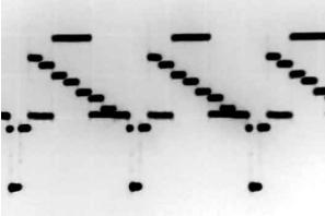 P7402-51 REC/PLAY1.0Vp-p (20 μ sec.div) P7402-51 REC/PLAY1.0Vp-p (20 μ sec.div) | 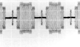 P7402-55 REC/PLAY0.8Vp-p (20 μ sec.div) P7402-55 REC/PLAY0.8Vp-p (20 μ sec.div) |
 P7402-59 REC/PLAY0.6Vp-p (20 μ sec.div) P7402-59 REC/PLAY0.6Vp-p (20 μ sec.div) |  P7402-63 REC/PLAY1.0Vp-p (20 μ sec.div) P7402-63 REC/PLAY1.0Vp-p (20 μ sec.div) |  P7402-67 REC/PLAY0.6Vp-p (20 μ sec.div) P7402-67 REC/PLAY0.6Vp-p (20 μ sec.div) |  P7402-71 REC/PLAY1.0Vp-p (20 μ sec.div) P7402-71 REC/PLAY1.0Vp-p (20 μ sec.div) |
 JK3903-2 REC/PLAY1.0Vp-p (20 μ sec.div) JK3903-2 REC/PLAY1.0Vp-p (20 μ sec.div) | 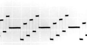 JK3903-4 REC/PLAY1.0Vp-p (20 μ sec.div) JK3903-4 REC/PLAY1.0Vp-p (20 μ sec.div) | 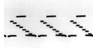 JK3903-6 REC/PLAY2.0Vp-p (20 μ sec.div) JK3903-6 REC/PLAY2.0Vp-p (20 μ sec.div) |
16 EXPLODED VIEWS
16.1. CASING PARTS AND MECHANISM SECTION
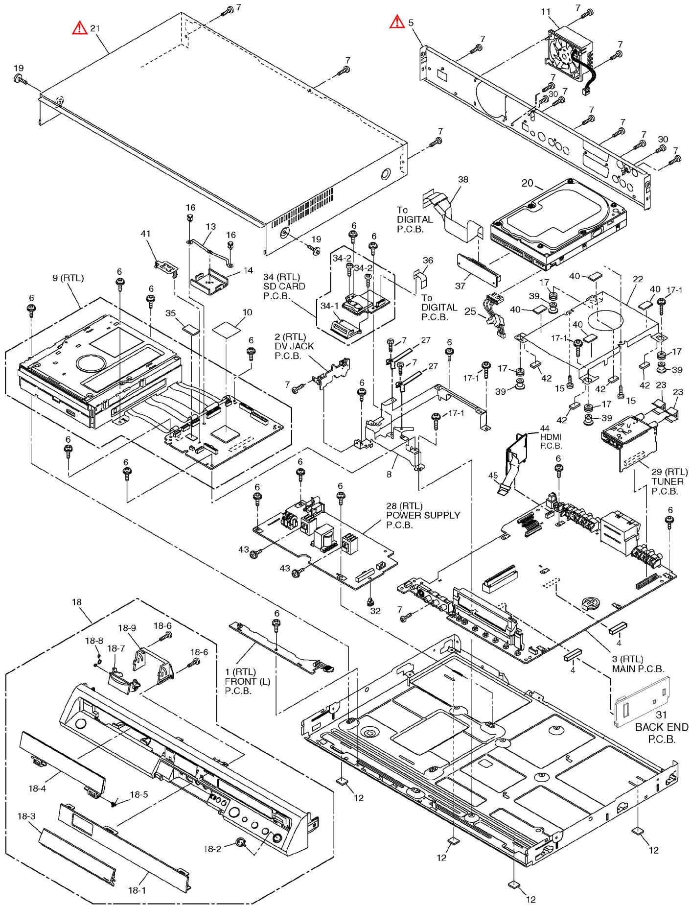
16.2. PACKING & ACCESSORIES SECTION
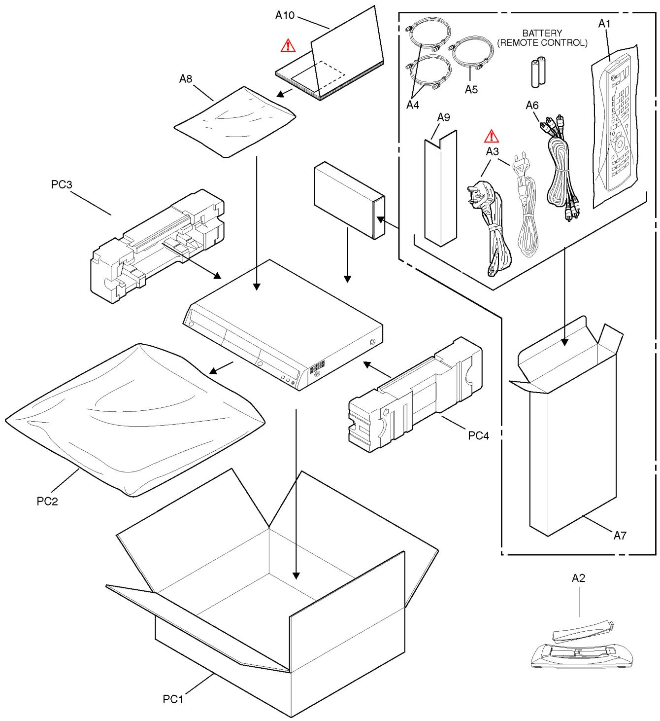
17 REPLACEMENT PARTS LIST
Notes:
*Important safety notice:
Components identified by ⚠️ mark have special characteristics important for safety.
Furthermore, special parts which have purposes of fire-retardant (resistors), high-quality sound (capacitors), low-noise (resistors), etc. are used.
When replacing any of components, be sure to use only manufactures specified parts shown in the parts list.
*Warning: This product uses a laser diode. Refer to caution statements.
*Capacity values are in microfarads (μF) unless specified otherwise, P=Pico-farads (pF), F=Farads (F).
*Resistance values are in ohms, unless specified otherwise, 1K=1,000 (OHM), 1M=1,000k (OHM).
*The marking (RTL) indicates the retention time is limited for this item. After the discontinuation of this assembly in production, it will no longer be available.
*All parts except parts mentioned [SPC] in the Remarks column are supplied from PAVCG.
*Parts mentioned [SPC] are supplied from PAVC
*The 1, 2, 3, 4, 5 in the Remarks column shows the models as follows:
1 = DMR - EX75EC - S
2 = DMR - EX75EG - S
3 = DMR-EX75EB-S
4 = DMR-EX85EB-S
5 = DMR - EX85EG - S
No indication = all models
17.1. CASING PARTS & PRINTED CIRCUIT BOARDS
| Ref. No. | Part No. | Part Name & Description | PCS | Remarks |
| █ 1 | REPD0030A | FRONT L PCB U | 1 | RTL1,2,3,4,5 |
| █ 2 | VEP73135A | DV JACK PCB UNIT | 1 | RTL1,2,3,4,5 |
| █ 3 | REPD0029D | MAIN PCB UNIT | 1 | RTL3,4 |
| ■ 3 | REPD0029FT | MAIN PCB UNIT | 1 | RTL1, |
| ■ 3 | REPD0029CT | MAIN PCB UNIT | 1 | RTL2,5 |
| 4 | RMX0364 | SPACER | 2 | 1,2,3,4,5 |
| 5 | RGR0365C-H1 | REAR PANEL | 1 | ;1,2 |
| 5 | RGR0365C-J1 | REAR PANEL | 1 | 3 |
| 5 | RGR0365C-L1 | REAR PANEL | 1 | 4 |
| 5 | RGR0365C-K1 | REAR PANEL | 1 | 5 |
| 6 | RHD30111-3 | SCREW | 16 | 1,2,3,4,5 |
| 7 | RHD30119-L | SCREW | 16 | 1,2,3,4,5 |
| 8 | RMA1979A | DIGITAL ANGLE A | 1 | 1,2,3,4,5 |
| █ 9 | RFKNEX75EC | RAM DIGITAL PCB MODULE | 1 | RTL1 |
| ■ 9 | RFKNEX75EG | RAM DIGITAL PCB MODULE | 1 | RTL2 |
| ■ 9 | RFKNEX75EB | RAM DIGITAL PCB MODULE | 1 | RTL3 |
| Ref. No. | Part No. | Part Name & Description | PCS | Remarks |
| ■ 9 | RFKNEX85EG | RAM DIGITAL PCB MODULE | 1 | RTL5 |
| ■ 9 | RFKNEX85EB | RAM DIGITAL PCB MODULE | 1 | RTL4 |
| 10 | RMQ1513 | HEAT TRANSFER SHEET | 1 | 1,2,3,4,5 |
| 11 | L6FAJDAE0001 | FAN MOTOR | 1 | 1,2,3,4,5 |
| 12 | RKA0144-K | FOOT RUBBER | 4 | 1,2,3,4,5 |
| 13 | RMC0672 | PLATE SPRING | 1 | 1,2,3,4,5 |
| 14 | RMY0357 | HEAT SINK | 1 | 1,2,3,4,5 |
| 15 | RHD32001 | SCREW WITH WASHER | 2 | 1,2,3,4,5 |
| 16 | VKC0295 | MINI CARD SPACER | 2 | 1,2,3,4,5 |
| 17 | RMG0704-W | DAMPER | 4 | 1,2,3,4,5 |
| 17-1 | RHD30149 | SCREW | 4 | 1,2,3,4,5 |
| 18 | RYP1326-S | FRONT PANEL U | 1 | 5 |
| 18 | RYP1326A-S | FRONT PANEL U | 1 | 4 |
| 18 | RYP1325A-S | FRONT PANEL U | 1 | 3 |
| 18 | RYP1325-S | FRONT PANEL U | 1 | 1,2 |
| 18-1 | RGK1969-S | FL ORNAMENT | 1 | 4,5 |
| 18-1 | RGK1968A-Q | FL ORNAMENT | 1 | 1,2,3, |
| 18-2 | RGK1971-S | REC BUTTON RING | 1 | 1,2,3,4,5 |
| 18-3 | RKF0753J-S | PANEL DOOR | 1 | 4,5 |
| 18-3 | RKF0753H-S | PANEL DOOR | 1 | 1,2,3 |
| 18-4 | RYF0785-K | TRAY DOOR UNIT | 1 | 4,5 |
| 18-4 | RYF0782C-K | TRAY DOOR UNIT | 1 | 1,2,3 |
| 18-5 | VMB3410 | BLINDER SPRING | 1 | 1,2,3,4,5 |
| 18-6 | RHD26045 | SCREW (PANEL) | 2 | 1,2,3,4,5 |
| 18-7 | RKF0754-K | SD BLINDER | 1 | 1,2,3,4,5 |
| 18-8 | RMB0841-1 | SD LID SPRING | 1 | 1,2,3,4,5 |
| 18-9 | RMR1767-K | SD CHASSIS | 1 | 1,2,3,4,5 |
| 19 | RHD30113 | SCREW TOP CASE SIDE | 2 | 1,2,3,4,5 |
| 20 | RFKV0069HDK | HDD ASSEMBLY | 1 | 1,2,3 |
| 20 | RFKV0071HDK | HDD ASSEMBLY | 1 | 4,5 |
| 21 | RKM0552A-S | TOP PANEL | 1 | 1,2,3,4,5 |
| 22 | RMN0857 | HDD BRACKET | 1 | 1,2,3,4,5 |
| 23 | RMC0625 | TUNER GND | 2 | 1,2,3,4,5 |
| 25 | VEE0Z41 | MAIN-HDD CABLE U | 1 | 1,2,3,4,5 |
| 27 | VMC1534 | EARTH SPRING (T) | 2 | 1,2,3,4,5 |
| █ 28 | VEP71110B | POWER PCB UNIT | 1 | RTL1,2,3,4,5 |
| █ 29 | REPD0032A | TUNER PCB UNIT | 1 | RTL2,5 |
| ■ 29 | REPD0032B | TUNER PCB UNIT | 1 | RTL3,4 |
| ■ 29 | REPD0032C | TUNER PCB UNIT | 1 | RTL1 |
| 30 | XSN3+4FJ | SCREW (TUNER) | 2 | 1,2,3,4,5 |
| █ 31 | REPD0031A | BACKEND PCB UNIT | 1 | RTL2,5 |
| ■ 31 | REPD0031C | BACKEND PCB UNIT | 1 | RTL3,4, |
| ■ 31 | REPD0031D | BACKEND PCB UNIT | 1 | RTL1, |
| 32 | VMX1336 | MINI CARD SPACER | 1 | 1,2,3,4,5 |
| █ 34 | VEP73136A | SD CARD PCB UNIT | 1 | 1,2,3,4,5 |
| 34-1 | RMR1766-K | SD CARD HOLDER | 1 | 1,2,3,4,5 |
| 34-2 | XTN2+8GFJ | SCREW | 2 | 1,2,3,4,5 |
| 35 | RMQ1514 | HEAT TRANSF. SHEET D | 1 | 1,2,3,4,5 |
| 36 | VWJ1877 | DIGITAL-SD FFC | 1 | 1,2,3,4,5 |
| 37 | N5EZZ0000003 | ATAPI CONNECTOR UNIT | 1 | 1,2,3,4,5 |
| 38 | REZD0026 | DIGITAL-HDD FFC | 1 | 1,2,3,4,5 |
| 39 | RMX0358 | SLEEVE | 4 | 1,2,3,4,5 |
| 40 | RMX0359 | HDD CUSHION SPACER | 4 | 1,2,3,4,5 |
| 41 | RMV0312 | SHEET COVER | 1 | 1,2,3,4,5 |
| 42 | RMX0362 | GEL SPACER | 4 | 1,2,3,4,5 |
| 43 | XYN3+J8FJ | SCREW | 2 | 1,2,3,4,5 |
| █ 44 | VEP73137AB | HDMI PCB U | 1 | RTL1,2,3,4,5 |
| 45 | VWJ1878 | DIGITAL-HDMI FFC | 1 | 1,2,3,4,5 |
17.2. PACKING & ACCESSORIES PARTS
| Ref. No. | Part No. | Part Name & Description | PCS | Remarks |
| A1 | EUR7659YM0 | REMOTE CONTROL | 1 | 2,5 |
| A1 | EUR7659YG0 | REMOTE CONTROL | 1 | 3,4 |
| A1 | EUR7659T40 | REMOTE CONTROL | 1 | 1 |
| A2 | UR76EC5903 | BATTERY COVER | 1 | 1,2,3,4,5 |
| A3 | RJA0043-1C | POWERCORD | 1 | 1,2,5 |
| A3 | K2CT3CA00004 | POWERCORD UK | 1 | 3,4 |
| A4 | K1TWACC00001 | RF CABLE | 2 | 1,2,3,4,5 |
| A5 | K1TWACA00001 | RF CABLE | 1 | 3,4 |
| A6 | K2KA6BA00003 | AV CORD | 1 | 1,2,3,4,5 |
| A7 | RPQFD0001 | ACCESSORY BOX | 1 | 1,2,3,4,5 |
| A8 | RPFD0007 | PE-BAG,24cmx37cmx40 | 1 | 3,4 |
| A8 | RPFD0005 | PE-BAG,28cmx41cmx40 | 1 | 1,2,5 |
| A9 | RPQD0003 | PAD (C) | 1 | 1,2,3,4,5 |
| A10 | RQTD0211-A | O/I BOOK ENG CONT | 1 | 2,5 |
| A10 | RQTD0216-A | O/I BOOK ENG CONT | 1 | 1 |
| A10 | RQTD0214-1B | O/I BOOK ENG UK | 1 | 3,4 |
| A10 | RQTD0212-C | O/I BOOK FRE | 1 | 1 |
| A10 | RQTD0210-D | O/I BOOK GER | 1 | 2,5 |
| A10 | RQTD0215-V | O/I BOOK ITA | 1 | 1 |
| A10 | RQTD0213-M | O/I BOOK SPA | 1 | 1 |
| A10 | RQCC2704 | DVD-MEDIA LEAFLET | 1 | 1,2,3,4,5 |
| A10 | RQCAD0032 | QUICK START GUIDE | 1 | 3,4 |
| A10 | RQCAD0034 | REFERENCE GUIDE | 1 | 3,4 |
| A10 | RQCB1293 | REGISTRATION LEAFLET | 1 | 1,2,5 |
| PC1 | RPG7861-1 | CARTON BOX | 1 | 3 |
| PC1 | RPG7860-2 | CARTON BOX | 1 | 1 |
| PC1 | RPG7859-1 | CARTON BOX | 1 | 2 |
| PC1 | RPG8020-2 | CARTON BOX | 1 | 4 |
| PC1 | RPG8019-2 | CARTON BOX | 1 | 5 |
| PC2 | RPFD0004 | MIRAMAT BAG | 1 | 1,2,3,4,5 |
| PC3 | RPN1859A-2 | CUSHION(LEFT) | 1 | 1,2,3,4,5 |
| PC4 | RPN1859B-2 | CUSHION(RIGHT) | 1 | 1,2,3,4,5 |
17.3. ELECTRICAL PARTS
| Ref. No. | Part No. | Part Name & Description | PCS | Remarks |
| C1120 | ECQU2A683MLC | X2 CAPACITOR | 1 | 1,2,3,4,5 |
| C1121 | ECQU2A223MLC | EMI CAPACITOR | 1 | 1,2,3,4,5 |
| C1122 | ECKWNA102MEV | CERAMIC CAPACITOR | 1 | 1,2,3,4,5 |
| C1123 | ECKWNA102MEV | CERAMIC CAPACITOR | 1 | 1,2,3,4,5 |
| C1125 | ECKWNA102MEV | CERAMIC CAPACITOR | 1 | 1,2,3,4,5 |
| C1143 | F2B2W4700003 | ALU ELEC CAPACITOR | 1 | 1,2,3,4,5 |
| C1150 | F2A1V6800002 | ALU ELEC CAPACITOR | 1 | 1,2,3,4,5 |
| C1151 | F1B3D102A011 | CERAMIC CAPACITOR | 1 | 1,2,3,4,5 |
| C1152 | ECJ2VC1H331J | CHIP CAPACITOR | 1 | 1,2,3,4,5 |
| C1153 | ECJGVB1H222K | CHIP CAPACITOR | 1 | 1,2,3,4,5 |
| C1154 | ECJGVB1H102K | CHIP CAPACITOR | 1 | 1,2,3,4,5 |
| C1200 | F1J1E104A081 | CHIP CAPACITOR | 1 | 1,2,3,4,5 |
| C1201 | ECJ2VB1E473K | CHIP CAPACITOR | 1 | 1,2,3,4,5 |
| C1270 | F2A1C1820005 | ALU ELEC CAPACITOR | 1 | 1,2,3,4,5 |
| C1271 | F2A1C1820005 | ALU ELEC CAPACITOR | 1 | 1,2,3,4,5 |
| C1272 | F2A1C8210008 | ALU ELEC CAPACITOR | 1 | 1,2,3,4,5 |
| C1503 | F2A1A2210063 | ALU ELEC CAPACITOR | 1 | 1,2,3,4,5 |
| C1504 | F2A1E1010067 | ALU ELEC CAPACITOR | 1 | 1,2,3,4,5 |
| C1506 | F2A1A470A388 | ALU ELEC CAPACITOR | 1 | 1,2,3,4,5 |
| C1508 | ECJ1VB1A105K | CHIP CAPACITOR | 1 | 1,2,3,4,5 |
| C1509 | F1H1H1030007 | CHIP CAPACITOR | 1 | 1,2,3,4,5 |
| C1510 | ECJ1VB1A105K | CHIP CAPACITOR | 1 | 1,2,3,4,5 |
| C1511 | ECJ1VB1A105K | CHIP CAPACITOR | 1 | 1,2,3,4,5 |
| C1512 | ECJ1VB1A105K | CHIP CAPACITOR | 1 | 1,2,3,4,5 |
| C1515 | F2A1A470A388 | ALU ELEC CAPACITOR | 1 | 1,2,3,4,5 |
| C1516 | F2A1A4710038 | ALU ELEC CAPACITOR | 1 | 1,2,3,4,5 |
| Ref. No. | Part No. | Part Name & Description | PCS | Remarks |
| C1518 | F2A0J681A550 | ALU ELEC CAPACITOR | 1 | 1,2,3,4,5 |
| C1519 | ECJ1VB1A105K | CHIP CAPACITOR | 1 | 1,2,3,4,5 |
| C1520 | ECJ3FB1C105K | CHIP CAPACITOR | 1 | 1,2,3,4,5 |
| C1522 | F1H1H1030007 | CHIP CAPACITOR | 1 | 1,2,3,4,5 |
| C1523 | F2A1A470A388 | ALU ELEC CAPACITOR | 1 | 1,2,3,4,5 |
| C1524 | F2A1A101A389 | ALU ELEC CAPACITOR | 1 | 1,2,3,4,5 |
| C1526 | ECJ2FB1A225K | CHIP CAPACITOR | 1 | 1,2,3,4,5 |
| C1527 | F1H1H1020005 | CHIP CAPACITOR | 1 | 1,2,3,4,5 |
| C1528 | F1H1E104A030 | CHIP CAPACITOR | 1 | 1,2,3,4,5 |
| C1529 | F1H1H1030007 | CHIP CAPACITOR | 1 | 1,2,3,4,5 |
| C1530 | F2A1E1010103 | ALU ELEC CAPACITOR | 1 | 1,2,3,4,5 |
| C1531 | ECJ1VB1A334K | CHIP CAPACITOR | 1 | 1,2,3,4,5 |
| C1532 | ECJ1VB1H331K | CHIP CAPACITOR | 1 | 1,2,3,4,5 |
| C1533 | F2A0J681A550 | ALU ELEC CAPACITOR | 1 | 1,2,3,4,5 |
| C1534 | F1H1E104A030 | CHIP CAPACITOR | 1 | 1,2,3,4,5 |
| C1535 | F2A1E3310051 | ALU ELEC CAPACITOR | 1 | 1,2,3,4,5 |
| C1538 | ECJ1VB1A105K | CHIP CAPACITOR | 1 | 1,2,3,4,5 |
| C1539 | ECJ1VB1A105K | CHIP CAPACITOR | 1 | 1,2,3,4,5 |
| C1540 | F1H1H1030007 | CHIP CAPACITOR | 1 | 1,2,3,4,5 |
| C1541 | F2A1E1010067 | ALU ELEC CAPACITOR | 1 | 1,2,3,4,5 |
| C1601 | F2A1E2210050 | ALU ELEC CAPACITOR | 1 | 1,2,3,4,5 |
| C1602 | F1J1E104A081 | CHIP CAPACITOR | 1 | 1,2,3,4,5 |
| C1603 | F1J1E104A081 | CHIP CAPACITOR | 1 | 1,2,3,4,5 |
| C1604 | ECJ2YB1C474K | CHIP CAPACITOR | 1 | 1,2,3,4,5 |
| C1605 | ECJ2VC1H181J | CHIP CAPACITOR | 1 | 1,2,3,4,5 |
| C1606 | ECJGVB1H103K | CHIP CAPACITOR | 1 | 1,2,3,4,5 |
| C1607 | F2A1A6810022 | ALU ELEC CAPACITOR | 1 | 1,2,3,4,5 |
| C1608 | F1J1E104A081 | CHIP CAPACITOR | 1 | 1,2,3,4,5 |
| C1701 | F2A1E2210050 | ALU ELEC CAPACITOR | 1 | 1,2,3,4,5 |
| C1702 | F1H1C104A042 | CHIP CAPACITOR | 1 | 1,2,3,4,5 |
| C1703 | F1H1C104A042 | CHIP CAPACITOR | 1 | 1,2,3,4,5 |
| C1704 | F1H1C104A042 | CHIP CAPACITOR | 1 | 1,2,3,4,5 |
| C1705 | ECJ1VC1H181J | CHIP CAPACITOR | 1 | 1,2,3,4,5 |
| C1706 | F1H1H1030006 | CHIP CAPACITOR | 1 | 1,2,3,4,5 |
| C1707 | F2A0J6810007 | ALU ELEC CAPACITOR | 1 | 1,2,3,4,5 |
| C1800 | F2A1E4700048 | ALU ELEC CAPACITOR | 1 | 1,2,3,4,5 |
| C3001 | F1H1E104A030 | CHIP CAPACITOR | 1 | 1,2,3,4,5 |
| C3002 | F1H1H1030007 | CHIP CAPACITOR | 1 | 1,2,3,4,5 |
| C3003 | F1H1E104A030 | CHIP CAPACITOR | 1 | 1,2,3,4,5 |
| C3004 | F1H1E104A030 | CHIP CAPACITOR | 1 | 1,2,3,4,5 |
| C3005 | F2A0J471A016 | ALU ELEC CAPACITOR | 1 | 1,2,3,4,5 |
| C3006 | F2A0J471A016 | ALU ELEC CAPACITOR | 1 | 1,2,3,4,5 |
| C3007 | F2A0J471A016 | ALU ELEC CAPACITOR | 1 | 1,2,3,4,5 |
| C3008 | F2A1A1010072 | ALU ELEC CAPACITOR | 1 | 1,2,3,4,5 |
| C3009 | F2A0J471A016 | ALU ELEC CAPACITOR | 1 | 1,2,3,4,5 |
| C3010 | F2A1A1010072 | ALU ELEC CAPACITOR | 1 | 1,2,3,4,5 |
| C3011 | F1H1E104A030 | CHIP CAPACITOR | 1 | 1,2,3,4,5 |
| C3012 | F2A0J471A016 | ALU ELEC CAPACITOR | 1 | 1,2,3,4,5 |
| C3013 | F2A1E4700048 | ALU ELEC CAPACITOR | 1 | 1,2,3,4,5 |
| C3014 | F1H1E104A030 | CHIP CAPACITOR | 1 | 1,2,3,4,5 |
| C3015 | F1H1E104A030 | CHIP CAPACITOR | 1 | 1,2,3,4,5 |
| C3016 | F1H1E104A030 | CHIP CAPACITOR | 1 | 1,2,3,4,5 |
| C3017 | F1H1E104A030 | CHIP CAPACITOR | 1 | 1,2,3,4,5 |
| C3018 | F1H1E104A030 | CHIP CAPACITOR | 1 | 1,2,3,4,5 |
| C3019 | F1H1E104A030 | CHIP CAPACITOR | 1 | 1,2,3,4,5 |
| C3020 | F1H1E104A030 | CHIP CAPACITOR | 1 | 1,2,3,4,5 |
| C3021 | F1H1E104A030 | CHIP CAPACITOR | 1 | 1,2,3,4,5 |
| C3022 | F1H1E104A030 | CHIP CAPACITOR | 1 | 1,2,3,4,5 |
| C3023 | F1H1H330A736 | CHIP CAPACITOR | 1 | 1,2,3,4,5 |
| C3025 | F1H1E104A030 | CHIP CAPACITOR | 1 | 1,2,3,4,5 |
| C3026 | ECJ1VF1C105Z | CHIP CAPACITOR | 1 | 1,2,3,4,5 |
| C3027 | F1H1E104A030 | CHIP CAPACITOR | 1 | 1,2,3,4,5 |
| C3028 | ECJ1VB1A105K | CHIP CAPACITOR | 1 | 1,2,3,4,5 |
| C3029 | F1H1E104A030 | CHIP CAPACITOR | 1 | 1,2,3,4,5 |
| C3030 | ECJ1VB1A105K | CHIP CAPACITOR | 1 | 1,2,3,4,5 |
| C3031 | ECJ1VF1C105Z | CHIP CAPACITOR | 1 | 1,2,3,4,5 |
| C3032 | ECEA0JKA101B | ALU ELEC CAPACITOR | 1 | 1,2,3,4,5 |
| C3033 | ECJ1VF1C105Z | CHIP CAPACITOR | 1 | 1,2,3,4,5 |
| C3034 | F1H1H1030007 | CHIP CAPACITOR | 1 | 1,2,3,4,5 |
| C3035 | ECEA0JKA101B | ALU ELEC CAPACITOR | 1 | 1,2,3,4,5 |
| C3036 | F1H1E104A030 | CHIP CAPACITOR | 1 | 1,2,3,4,5 |
| C3037 | F1H1E104A030 | CHIP CAPACITOR | 1 | 1,2,3,4,5 |
| C3038 | ECJ1VC1H100D | CHIP CAPACITOR | 1 | 1,2,3,4,5 |
DMR-EX75EG / DMR-EX75EC / DMR-EX75EB / DMR-EX85EG / DMR-EX85EB
| Ref. No. | Part No. | Part Name & Description | PCS | Remarks |
| C3039 | ECJ1VC1H100D | CHIP CAPACITOR | 1 | 1,2,3,4,5 |
| C3040 | ECJ1VC1H100D | CHIP CAPACITOR | 1 | 1,2,3,4,5 |
| C3041 | ECJ1VC1H100D | CHIP CAPACITOR | 1 | 1,2,3,4,5 |
| C3042 | ECJ1VC1H100D | CHIP CAPACITOR | 1 | 1,2,3,4,5 |
| C3043 | ECJ1VC1H100D | CHIP CAPACITOR | 1 | 1,2,3,4,5 |
| C3044 | ECJ1VC1H100D | CHIP CAPACITOR | 1 | 1,2,3,4,5 |
| C3057 | ECJ1VB1H471K | CHIP CAPACITOR | 1 | 1,2,3,4,5 |
| C3058 | ECJ1VB1H471K | CHIP CAPACITOR | 1 | 1,2,3,4,5 |
| C3059 | ECJ1VB1H471K | CHIP CAPACITOR | 1 | 1,2,3,4,5 |
| C3060 | ECJ1VB1H471K | CHIP CAPACITOR | 1 | 1,2,3,4,5 |
| C3064 | F1H1E104A030 | CHIP CAPACITOR | 1 | 1,2,3,4,5 |
| C3065 | ECJ1VF1C105Z | CHIP CAPACITOR | 1 | 1,2,3,4,5 |
| C3070 | ECJ1VB1H471K | CHIP CAPACITOR | 1 | 1,2,3,4,5 |
| C3071 | ECJ1VB1H471K | CHIP CAPACITOR | 1 | 1,2,3,4,5 |
| C3072 | F1H1E104A030 | CHIP CAPACITOR | 1 | 1,2,3,4,5 |
| C3910 | F2A1V100A534 | ALU ELEC CAPACITOR | 1 | 1,2,3,4,5 |
| C3911 | F2A1V100A534 | ALU ELEC CAPACITOR | 1 | 1,2,3,4,5 |
| C3914 | F2A1H100A236 | ALU ELEC CAPACITOR | 1 | 1,2,3,4,5 |
| C3915 | F2A1H100A236 | ALU ELEC CAPACITOR | 1 | 1,2,3,4,5 |
| C3916 | F2A1H1R0A236 | ALU ELEC CAPACITOR | 1 | 1,2,3,4,5 |
| C3917 | F2A1H1R0A236 | ALU ELEC CAPACITOR | 1 | 1,2,3,4,5 |
| C3918 | F2A1H100A236 | ALU ELEC CAPACITOR | 1 | 1,2,3,4,5 |
| C3919 | F2A1H100A236 | ALU ELEC CAPACITOR | 1 | 1,2,3,4,5 |
| C3928 | F2A1V100A534 | ALU ELEC CAPACITOR | 1 | 1,2,3,4,5 |
| C3929 | F2A1V100A534 | ALU ELEC CAPACITOR | 1 | 1,2,3,4,5 |
| C3935 | F2A1E2210050 | ALU ELEC CAPACITOR | 1 | 1,2,3,4,5 |
| C3951 | F1H1H4700004 | CHIP CAPACITOR | 1 | 1,2,3,4,5 |
| C3952 | F1H1H4700004 | CHIP CAPACITOR | 1 | 1,2,3,4,5 |
| C3953 | ECJ1VB1H471K | CHIP CAPACITOR | 1 | 1,2,3,4,5 |
| C3954 | ECJ1VB1H471K | CHIP CAPACITOR | 1 | 1,2,3,4,5 |
| C3955 | F1H1H1010005 | CHIP CAPACITOR | 1 | 1,2,3,4,5 |
| C3956 | F1H1H1010005 | CHIP CAPACITOR | 1 | 1,2,3,4,5 |
| C3957 | ECJ1VB1H471K | CHIP CAPACITOR | 1 | 1,2,3,4,5 |
| C3958 | ECJ1VB1H471K | CHIP CAPACITOR | 1 | 1,2,3,4,5 |
| C3959 | F1H1H4700004 | CHIP CAPACITOR | 1 | 1,2,3,4,5 |
| C3960 | F1H1H4700004 | CHIP CAPACITOR | 1 | 1,2,3,4,5 |
| C3961 | F1H1H1010005 | CHIP CAPACITOR | 1 | 1,2,3,4,5 |
| C3962 | F1H1H1010005 | CHIP CAPACITOR | 1 | 1,2,3,4,5 |
| C4005 | F2A1H100A638 | ALU ELEC CAPACITOR | 1 | 1,2,3,4,5 |
| C4006 | F2A1H100A638 | ALU ELEC CAPACITOR | 1 | 1,2,3,4,5 |
| C4008 | F2A1E1010067 | ALU ELEC CAPACITOR | 1 | 1,2,3,4,5 |
| C4019 | F2A1C220A637 | ALU ELEC CAPACITOR | 1 | 1,2,3,4,5 |
| C4021 | F2A1C220A637 | ALU ELEC CAPACITOR | 1 | 1,2,3,4,5 |
| C4023 | F2A1H1R0A236 | ALU ELEC CAPACITOR | 1 | 1,2,3,4,5 |
| C4024 | F2A1E1010067 | ALU ELEC CAPACITOR | 1 | 1,2,3,4,5 |
| C4025 | F2A1H1R0A236 | ALU ELEC CAPACITOR | 1 | 1,2,3,4,5 |
| C4027 | F2A1H100A638 | ALU ELEC CAPACITOR | 1 | 1,2,3,4,5 |
| C4028 | F2A1H100A638 | ALU ELEC CAPACITOR | 1 | 1,2,3,4,5 |
| C4030 | F1H1H472A219 | CHIP CAPACITOR | 1 | 1,2,3,4,5 |
| C4031 | F1H1H472A219 | CHIP CAPACITOR | 1 | 1,2,3,4,5 |
| C4033 | F2A1C220B173 | ALU ELEC CAPACITOR | 1 | 1,2,3,4,5 |
| C4034 | F2A1C220B173 | ALU ELEC CAPACITOR | 1 | 1,2,3,4,5 |
| C4052 | F1H1E104A030 | CHIP CAPACITOR | 1 | 1,2,3,4,5 |
| C4053 | F2A1H100A638 | ALU ELEC CAPACITOR | 1 | 1,2,3,4,5 |
| C4054 | F2A1H100A638 | ALU ELEC CAPACITOR | 1 | 1,2,3,4,5 |
| C4055 | F1H1E104A030 | CHIP CAPACITOR | 1 | 1,2,3,4,5 |
| C4056 | F2A1C471A628 | ALU ELEC CAPACITOR | 1 | 1,2,3,4,5 |
| C4057 | ECJ2VC1H330J | CHIP CAPACITOR | 1 | 1,2,3,4,5 |
| C4059 | ECQV1H104JL2 | PLAST FILM CAPACITOR | 1 | 1,2,3,4,5 |
| C4060 | ECJ2VC1H330J | CHIP CAPACITOR | 1 | 1,2,3,4,5 |
| C4061 | F1H1E104A030 | CHIP CAPACITOR | 1 | 1,2,3,4,5 |
| C4062 | F2A1A221A206 | ALU ELEC CAPACITOR | 1 | 1,2,3,4,5 |
| C4063 | F2A1C220B173 | ALU ELEC CAPACITOR | 1 | 1,2,3,4,5 |
| C4064 | F2A1C220B173 | ALU ELEC CAPACITOR | 1 | 1,2,3,4,5 |
| C4065 | F1H1H1010005 | CHIP CAPACITOR | 1 | 1,2,3,4,5 |
| C4066 | F1H1H1010005 | CHIP CAPACITOR | 1 | 1,2,3,4,5 |
| C4067 | F2A1E4700048 | ALU ELEC CAPACITOR | 1 | 1,2,3,4,5 |
| C4082 | ECJ2VC1H561J | CHIP CAPACITOR | 1 | 1,2,3,4,5 |
| C4083 | ECJ2VC1H561J | CHIP CAPACITOR | 1 | 1,2,3,4,5 |
| C4092 | F2A1E2210050 | ALU ELEC CAPACITOR | 1 | 1,2,3,4,5 |
| C4903 | F2A1E4700048 | ALU ELEC CAPACITOR | 1 | 1,2,3,4,5 |
| C4904 | F1H1E104A030 | CHIP CAPACITOR | 1 | 1,2,3,4,5 |
| C56001 | ECJ0EC1H221J | CHIP CAPACITOR | 1 | 1,2,3,4,5 |
| Ref. No. | Part No. | Part Name & Description | PCS | Remarks |
| C56101 | ECJ0EB1A104K | CHIP CAPACITOR | 1 | 1,2,3,4,5 |
| C56102 | ECJ0EB1A104K | CHIP CAPACITOR | 1 | 1,2,3,4,5 |
| C56103 | ECJ0EB1A104K | CHIP CAPACITOR | 1 | 1,2,3,4,5 |
| C56104 | ECJ0EB1A104K | CHIP CAPACITOR | 1 | 1,2,3,4,5 |
| C56105 | ECJ0EB1A104K | CHIP CAPACITOR | 1 | 1,2,3,4,5 |
| C56106 | ECJ0EB1A104K | CHIP CAPACITOR | 1 | 1,2,3,4,5 |
| C56107 | ECJ0EB1A104K | CHIP CAPACITOR | 1 | 1,2,3,4,5 |
| C56108 | ECJ0EB1A104K | CHIP CAPACITOR | 1 | 1,2,3,4,5 |
| C56109 | ECJ0EB1A104K | CHIP CAPACITOR | 1 | 1,2,3,4,5 |
| C56110 | ECJ0EB1A104K | CHIP CAPACITOR | 1 | 1,2,3,4,5 |
| C56111 | ECJ0EB1A104K | CHIP CAPACITOR | 1 | 1,2,3,4,5 |
| C56112 | ECJ0EB1A104K | CHIP CAPACITOR | 1 | 1,2,3,4,5 |
| C56113 | ECJ0EB1A104K | CHIP CAPACITOR | 1 | 1,2,3,4,5 |
| C56114 | ECJ0EB1A104K | CHIP CAPACITOR | 1 | 1,2,3,4,5 |
| C56115 | ECJ0EB1A104K | CHIP CAPACITOR | 1 | 1,2,3,4,5 |
| C56116 | ECJ0EB1A104K | CHIP CAPACITOR | 1 | 1,2,3,4,5 |
| C56117 | ECJ0EB1A104K | CHIP CAPACITOR | 1 | 1,2,3,4,5 |
| C56118 | ECJ0EB1A104K | CHIP CAPACITOR | 1 | 1,2,3,4,5 |
| C56119 | ECJ0EB1A104K | CHIP CAPACITOR | 1 | 1,2,3,4,5 |
| C56120 | ECJ0EB1A104K | CHIP CAPACITOR | 1 | 1,2,3,4,5 |
| C56121 | ECJ0EB1A104K | CHIP CAPACITOR | 1 | 1,2,3,4,5 |
| C56122 | ECJ0EB1A104K | CHIP CAPACITOR | 1 | 1,2,3,4,5 |
| C56123 | ECJ0EB1A104K | CHIP CAPACITOR | 1 | 1,2,3,4,5 |
| C56124 | ECJ0EB1A104K | CHIP CAPACITOR | 1 | 1,2,3,4,5 |
| C56125 | ECJ0EB1A104K | CHIP CAPACITOR | 1 | 1,2,3,4,5 |
| C56126 | ECJ0EB1A104K | CHIP CAPACITOR | 1 | 1,2,3,4,5 |
| C56127 | ECJ0EB1A104K | CHIP CAPACITOR | 1 | 1,2,3,4,5 |
| C56128 | ECJ0EB1A104K | CHIP CAPACITOR | 1 | 1,2,3,4,5 |
| C56129 | ECJ0EC1H221J | CHIP CAPACITOR | 1 | 1,2,3,4,5 |
| C56130 | F1H0J1050012 | CHIP CAPACITOR | 1 | 1,2,3,4,5 |
| C56131 | F1J0J106A014 | CHIP CAPACITOR | 1 | 1,2,3,4,5 |
| C56132 | ECJ0EB1C103K | CHIP CAPACITOR | 1 | 1,2,3,4,5 |
| C56133 | ECJ1VB1A105K | CHIP CAPACITOR | 1 | 1,2,3,4,5 |
| C56134 | ECJ1VB1A105K | CHIP CAPACITOR | 1 | 1,2,3,4,5 |
| C56135 | ECJ0EB1A104K | CHIP CAPACITOR | 1 | 1,2,3,4,5 |
| C56140 | ECJ0EB1A104K | CHIP CAPACITOR | 1 | 1,2,3,4,5 |
| C6801 | F1H1H1030006 | CHIP CAPACITOR | 1 | 1,2,3,4,5 |
| C6802 | F1H1A225A051 | CHIP CAPACITOR | 1 | 1,2,3,4,5 |
| C7301 | F1H1H1030007 | CHIP CAPACITOR | 1 | 1,2,3,4,5 |
| C7302 | ECEA0JKA101B | ALU ELEC CAPACITOR | 1 | 1,2,3,4,5 |
| C7303 | F1H1H1030007 | CHIP CAPACITOR | 1 | 1,2,3,4,5 |
| C7304 | F1H1E104A030 | CHIP CAPACITOR | 1 | 1,2,3,4,5 |
| C7305 | F1H1H330A736 | CHIP CAPACITOR | 1 | 1,2,3,4,5 |
| C7306 | F1H1H330A736 | CHIP CAPACITOR | 1 | 1,2,3,4,5 |
| C7307 | F1H1H332A219 | CHIP CAPACITOR | 1 | 2,5 |
| C7308 | ECJ1VC1H681J | CHIP CAPACITOR | 1 | 2,5 |
| C7308 | D0GB822JA057 | CHIP RESISTOR | 1 | 1,2,3,4,5 |
| C7309 | F1H1H332A219 | CHIP CAPACITOR | 1 | 2,5 |
| C7310 | ECJ1VC1H681J | CHIP CAPACITOR | 1 | 2,5 |
| C7311 | F1H1H1030007 | CHIP CAPACITOR | 1 | 1,2,3,4,5 |
| C7312 | F1H1C104A042 | CHIP CAPACITOR | 1 | 1,2,3,4,5 |
| C7313 | ECJ1VF1C474Z | CHIP CAPACITOR | 1 | 2,5 |
| C7314 | F1H1H1030006 | CHIP CAPACITOR | 1 | 1,2,3,4,5 |
| C7314 | F1H1C104A042 | CHIP CAPACITOR | 1 | 1,2,3,4,5 |
| C7315 | F1H1H9R0A735 | CHIP CAPACITOR | 1 | 2,5 |
| C7316 | F1H1E104A030 | CHIP CAPACITOR | 1 | 1,2,3,4,5 |
| C7317 | ECJ1VB1H152K | CHIP CAPACITOR | 1 | 1,2,3,4,5 |
| C7318 | ECEA0JKA470B | ALU ELEC CAPACITOR | 1 | 1,2,3,4,5 |
| C7319 | ECEA1CKA100B | ALU ELEC CAPACITOR | 1 | 1,2,3,4,5 |
| C7320 | ECEA1CKA100B | ALU ELEC CAPACITOR | 1 | 1,2,3,4,5 |
| C7321 | F1H1H472A219 | CHIP CAPACITOR | 1 | 1,2,3,4,5 |
| C7322 | ECJ1VF1C474Z | CHIP CAPACITOR | 1 | 2,5 |
| C7323 | F1H1E104A030 | CHIP CAPACITOR | 1 | 1,2,3,4,5 |
| C7325 | F1H1H1030006 | CHIP CAPACITOR | 1 | 1,2,3,4,5 |
| C7327 | ECJ1VB1H152K | CHIP CAPACITOR | 1 | 1,2,3,4,5 |
| C7328 | ECJ1VF1C474Z | CHIP CAPACITOR | 1 | 2,5 |
| C7328 | F1H1E104A030 | CHIP CAPACITOR | 1 | 1,2,3,4,5 |
| C7329 | ECJ1VF1C474Z | CHIP CAPACITOR | 1 | 2,5 |
| C7330 | F1H1C104A042 | CHIP CAPACITOR | 1 | 1,2,3,4,5 |
| C7331 | F1J1C4740012 | CHIP CAPACITOR | 1 | 2,5 |
| C7331 | F1J1A105A003 | CHIP CAPACITOR | 1 | 1,3,4 |
| C7343 | ECEA0JKA101B | ALU ELEC CAPACITOR | 1 | 1,2,3,4,5 |
| C7402 | F1H1H1030007 | CHIP CAPACITOR | 1 | 1,2,3,4,5 |
| C7404 | ECJ1VB1A105K | CHIP CAPACITOR | 1 | 1,2,3,4,5 |
| C7406 | ECJ1VB1A105K | CHIP CAPACITOR | 1 | 1,2,3,4,5 |
| C7412 | F1H1H1030007 | CHIP CAPACITOR | 1 | 1,2,3,4,5 |
| C7413 | F1H1H1030007 | CHIP CAPACITOR | 1 | 1,2,3,4,5 |
| C7417 | F1H1E104A030 | CHIP CAPACITOR | 1 | 1,2,3,4,5 |
| C7418 | ECJ1VB1A105K | CHIP CAPACITOR | 1 | 1,2,3,4,5 |
| C7419 | ECJ1VB1A105K | CHIP CAPACITOR | 1 | 1,2,3,4,5 |
| C7420 | F2A1A2210063 | ALU ELEC CAPACITOR | 1 | 1,2,3,4,5 |
| C7439 | F1H1E104A030 | CHIP CAPACITOR | 1 | 1,2,3,4,5 |
| C7440 | F1H1E104A030 | CHIP CAPACITOR | 1 | 1,2,3,4,5 |
| C7501 | ECJ1VB1A105K | CHIP CAPACITOR | 1 | 1,2,3,4,5 |
| C7502 | F1H1H1010005 | CHIP CAPACITOR | 1 | 1,2,3,4,5 |
| C7503 | ECJ1VB1A105K | CHIP CAPACITOR | 1 | 1,2,3,4,5 |
| C7504 | F1H1E104A030 | CHIP CAPACITOR | 1 | 1,2,3,4,5 |
| C7505 | F1H1E104A030 | CHIP CAPACITOR | 1 | 1,2,3,4,5 |
| C7506 | ECJ1VB1H221K | CHIP CAPACITOR | 1 | 1,2,3,4,5 |
| C7507 | F1H1E104A030 | CHIP CAPACITOR | 1 | 1,2,3,4,5 |
| C7508 | ECJ1VB1H221K | CHIP CAPACITOR | 1 | 1,2,3,4,5 |
| C7509 | F1H1E104A030 | CHIP CAPACITOR | 1 | 1,2,3,4,5 |
| C7510 | F1H1E104A030 | CHIP CAPACITOR | 1 | 1,2,3,4,5 |
| C7511 | F1H1H1010005 | CHIP CAPACITOR | 1 | 1,2,3,4,5 |
| C7512 | F1H1E104A030 | CHIP CAPACITOR | 1 | 1,2,3,4,5 |
| C7513 | ECJ1VC1H100D | CHIP CAPACITOR | 1 | 1,2,3,4,5 |
| C7515 | ECJ1VC1H100D | CHIP CAPACITOR | 1 | 1,2,3,4,5 |
| C7516 | ECJ1VC1H180J | CHIP CAPACITOR | 1 | 1,2,3,4,5 |
| C7517 | ECJ1VC1H180J | CHIP CAPACITOR | 1 | 1,2,3,4,5 |
| C7518 | ECJ1VC1H220J | CHIP CAPACITOR | 1 | 1,2,3,4,5 |
| C7519 | ECJ1VC1H180J | CHIP CAPACITOR | 1 | 1,2,3,4,5 |
| C7520 | F1H1H1030007 | CHIP CAPACITOR | 1 | 1,2,3,4,5 |
| C7522 | F1H1H1010005 | CHIP CAPACITOR | 1 | 1,2,3,4,5 |
| C7523 | F1H1H1030007 | CHIP CAPACITOR | 1 | 1,2,3,4,5 |
| C7524 | F1H1E104A030 | CHIP CAPACITOR | 1 | 1,2,3,4,5 |
| C7528 | F1H1E104A030 | CHIP CAPACITOR | 1 | 1,2,3,4,5 |
| C7531 | ECJ1VC1H100D | CHIP CAPACITOR | 1 | 1,2,3,4,5 |
| C7532 | ECJ1VC1H100D | CHIP CAPACITOR | 1 | 1,2,3,4,5 |
| C7534 | ECJ1VB1A105K | CHIP CAPACITOR | 1 | 1,2,3,4,5 |
| C7541 | F1H1H4700004 | CHIP CAPACITOR | 1 | 1,2,3,4,5 |
| C7542 | F1H1E104A030 | CHIP CAPACITOR | 1 | 1,2,3,4,5 |
| C7543 | F1H1H4700004 | CHIP CAPACITOR | 1 | 1,2,3,4,5 |
| C7544 | F1H1E104A030 | CHIP CAPACITOR | 1 | 1,2,3,4,5 |
| C7546 | ECJ1VF1C105Z | CHIP CAPACITOR | 1 | 1,2,3,4,5 |
| C7547 | ECJ1VF1C105Z | CHIP CAPACITOR | 1 | 1,2,3,4,5 |
| C7551 | F1H1E104A030 | CHIP CAPACITOR | 1 | 1,2,3,4,5 |
| C7554 | F1H1H1030007 | CHIP CAPACITOR | 1 | 1,2,3,4,5 |
| C7555 | D0YBR0000020 | CHIP RESISTOR | 1 | 1,2,3,4,5 |
| C7556 | ECJ1VC1H102J | CHIP CAPACITOR | 1 | 1,2,3,4,5 |
| C7557 | ECJ1VC1H102J | CHIP CAPACITOR | 1 | 1,2,3,4,5 |
| C7558 | ECJ1VC1H102J | CHIP CAPACITOR | 1 | 1,2,3,4,5 |
| C7565 | F2A1E2210050 | ALU ELEC CAPACITOR | 1 | 1,2,3,4,5 |
| C7569 | ECQB1H392KF3 | PLAST FILM CAPACITOR | 1 | 1,2,3,4,5 |
| C7570 | F2A1V470A006 | ALU ELEC CAPACITOR | 1 | 1,2,3,4,5 |
| C7571 | F2A1H100A003 | ALU ELEC CAPACITOR | 1 | 1,2,3,4,5 |
| C7572 | F2A1A2210005 | ALU ELEC CAPACITOR | 1 | 1,2,3,4,5 |
| C7573 | F2A1H100A003 | ALU ELEC CAPACITOR | 1 | 1,2,3,4,5 |
| C7577 | F1H1E104A030 | CHIP CAPACITOR | 1 | 1,2,3,4,5 |
| C7578 | ECEA0JKA221B | ALU ELEC CAPACITOR | 1 | 1,2,3,4,5 |
| C7584 | F4D55473A013 | ALU ELEC CAPACITOR | 1 | 1,2,3,4,5 |
| C7585 | F2A0J101A012 | ALU ELEC CAPACITOR | 1 | 1,2,3,4,5 |
| C7587 | ECJ1VB1A105K | CHIP CAPACITOR | 1 | 1,2,3,4,5 |
| C7592 | ECEA0JKA470B | ALU ELEC CAPACITOR | 1 | 1,2,3,4,5 |
| C7800 | F1H1E104A030 | CHIP CAPACITOR | 1 | 1,2,3,4,5 |
| C7801 | F1H1E104A030 | CHIP CAPACITOR | 1 | 1,2,3,4,5 |
| C7802 | F1H1E104A030 | CHIP CAPACITOR | 1 | 1,2,3,4,5 |
| C7803 | F1H1E104A030 | CHIP CAPACITOR | 1 | 1,2,3,4,5 |
| C7804 | ECEA0JKA470B | ALU ELEC CAPACITOR | 1 | 1,2,3,4,5 |
| C7805 | ECEA0JKA470B | ALU ELEC CAPACITOR | 1 | 1,2,3,4,5 |
| C7806 | ECEA1HKA010B | ALU ELEC CAPACITOR | 1 | 1,2,3,4,5 |
| C7807 | F1H1H1030007 | CHIP CAPACITOR | 1 | 1,2,3,4,5 |
| C7808 | F1H1H1030007 | CHIP CAPACITOR | 1 | 1,2,3,4,5 |
| C7809 | F1H1H1030007 | CHIP CAPACITOR | 1 | 1,2,3,4,5 |
| C7810 | F1H1H1030007 | CHIP CAPACITOR | 1 | 1,2,3,4,5 |
| C7811 | F1H1H330A736 | CHIP CAPACITOR | 1 | 1,2,3,4,5 |
| C7812 | F1H1H330A736 | CHIP CAPACITOR | 1 | 1,2,3,4,5 |
| Ref. No. | Part No. | Part Name & Description | PCS | Remarks |
| C7813 | ECEA1CKA220B | ALU ELEC CAPACITOR | 1 | 1,2,5 |
| C7814 | F1H1C104A042 | CHIP CAPACITOR | 1 | 1,2,3,4,5 |
| C7815 | ECJ1VB1A105K | CHIP CAPACITOR | 1 | 1,2,3,4,5 |
| C7816 | ECJ1VB1A105K | CHIP CAPACITOR | 1 | 1,2,3,4,5 |
| C7817 | ECJ1VB1A105K | CHIP CAPACITOR | 1 | 1,2,3,4,5 |
| C7818 | F1H1H1030007 | CHIP CAPACITOR | 1 | 1,2,3,4,5 |
| C7819 | F1H1H1030007 | CHIP CAPACITOR | 1 | 1,2,3,4,5 |
| C7820 | F1H1E104A030 | CHIP CAPACITOR | 1 | 1,2,3,4,5 |
| C7821 | F1H1H1030007 | CHIP CAPACITOR | 1 | 1,2,3,4,5 |
| C7822 | F1H1H1030007 | CHIP CAPACITOR | 1 | 1,2,3,4,5 |
| C7822 | F1H1H2700003 | CHIP CAPACITOR | 1 | 3,4 |
| C9001 | F1H1H1030006 | CHIP CAPACITOR | 1 | 1,2,3,4,5 |
| C9002 | F1H1H1030006 | CHIP CAPACITOR | 1 | 1,2,3,4,5 |
| C9003 | F1H1C104A042 | CHIP CAPACITOR | 1 | 1,2,3,4,5 |
| C9004 | F1H1H1030006 | CHIP CAPACITOR | 1 | 1,2,3,4,5 |
| C9005 | F1H1H1030006 | CHIP CAPACITOR | 1 | 1,2,3,4,5 |
| C9006 | ECJ1VC1H020C | CHIP CAPACITOR | 1 | 1,2,3,4,5 |
| C9007 | ECJ2FB1A225K | CHIP CAPACITOR | 1 | 1,2,3,4,5 |
| C9008 | F1H1C104A042 | CHIP CAPACITOR | 1 | 1,2,3,4,5 |
| C9009 | F1H1H1030006 | CHIP CAPACITOR | 1 | 1,2,3,4,5 |
| C9010 | F1H1H1030006 | CHIP CAPACITOR | 1 | 1,2,3,4,5 |
| C9011 | F1H1C104A042 | CHIP CAPACITOR | 1 | 1,2,3,4,5 |
| C9012 | ECJ1VC1H100C | CHIP CAPACITOR | 1 | 1,2,3,4,5 |
| C9012 | F1H1H1200004 | CHIP CAPACITOR | 1 | 1 |
| C9013 | ECJ1VC1H100C | CHIP CAPACITOR | 1 | 1,2,3,4,5 |
| C9013 | F1H1H1200004 | CHIP CAPACITOR | 1 | 1 |
| C9014 | F1H1C104A042 | CHIP CAPACITOR | 1 | 1,2,3,4,5 |
| C9038 | F1H1C104A042 | CHIP CAPACITOR | 1 | 1,2,3,4,5 |
| C9039 | ECJ1VB1H221K | CHIP CAPACITOR | 1 | 1,2,3,4,5 |
| C9040 | ECJ1VB1H221K | CHIP CAPACITOR | 1 | 1,2,3,4,5 |
| C9042 | F1H1C104A008 | CHIP CAPACITOR | 1 | 1,2,3,4,5 |
| C9201 | ECJ1VF1C105Z | CHIP CAPACITOR | 1 | 1,2,3,4,5 |
| C9202 | ECJ1VC1H102J | CHIP CAPACITOR | 1 | 1,2,3,4,5 |
| C9203 | F1H1C104A042 | CHIP CAPACITOR | 1 | 1,2,3,4,5 |
| C9204 | ECJ1VF1C334Z | CHIP CAPACITOR | 1 | 1,2,3,4,5 |
| C9205 | F1H1H1500009 | CHIP CAPACITOR | 1 | 1,2,3,4,5 |
| C9206 | F1H1H1030007 | CHIP CAPACITOR | 1 | 1,2,3,4,5 |
| C9207 | ECJ1VF1C105Z | CHIP CAPACITOR | 1 | 1,2,3,4,5 |
| C9208 | F1H1H1500009 | CHIP CAPACITOR | 1 | 1,2,3,4,5 |
| C9211 | ECJ1VB1H152K | CHIP CAPACITOR | 1 | 1,2,3,4,5 |
| C9212 | ECJ1VC1H100C | CHIP CAPACITOR | 1 | 1,2,3,4,5 |
| C9303 | F1H1H1030006 | CHIP CAPACITOR | 1 | 1,2,3,4,5 |
| C9305 | F1H1H1030006 | CHIP CAPACITOR | 1 | 1,2,3,4,5 |
| C9306 | F1H1H1030006 | CHIP CAPACITOR | 1 | 1,2,3,4,5 |
| C9307 | ECJ1VF1C105Z | CHIP CAPACITOR | 1 | 1,2,3,4,5 |
| C9308 | F1H1C104A008 | CHIP CAPACITOR | 1 | 1,2,3,4,5 |
| C9309 | ECJ1VF1C105Z | CHIP CAPACITOR | 1 | 1,2,3,4,5 |
| C9310 | ECJ1VF1C105Z | CHIP CAPACITOR | 1 | 1,2,3,4,5 |
| C9311 | ECJ1VF1C105Z | CHIP CAPACITOR | 1 | 1,2,3,4,5 |
| C9312 | F1H1C104A008 | CHIP CAPACITOR | 1 | 1,2,3,4,5 |
| C9313 | ECJ1VF1C105Z | CHIP CAPACITOR | 1 | 1,2,3,4,5 |
| C9501 | ECJ1VF1C105Z | CHIP CAPACITOR | 1 | 1,2,3,4,5 |
| C9502 | ECJ1VF1C105Z | CHIP CAPACITOR | 1 | 1,2,3,4,5 |
| C9503 | F1H1H1030006 | CHIP CAPACITOR | 1 | 1,2,3,4,5 |
| C9504 | F1H1H1030006 | CHIP CAPACITOR | 1 | 1,2,3,4,5 |
| C9505 | F1H1C104A042 | CHIP CAPACITOR | 1 | 1,2,3,4,5 |
| C9506 | F1H1C104A042 | CHIP CAPACITOR | 1 | 1,2,3,4,5 |
| C9507 | F1H1H1030006 | CHIP CAPACITOR | 1 | 1,2,3,4,5 |
| C9508 | F1H1C104A042 | CHIP CAPACITOR | 1 | 1,2,3,4,5 |
| C9509 | ECJ1VF1C105Z | CHIP CAPACITOR | 1 | 1,2,3,4,5 |
| C9510 | ECJ1VF1C105Z | CHIP CAPACITOR | 1 | 1,2,3,4,5 |
| C9511 | F1H1H4700004 | CHIP CAPACITOR | 1 | 1,2,3,4,5 |
| C9512 | F1H1H4700004 | CHIP CAPACITOR | 1 | 1,2,3,4,5 |
| C9513 | F1H1H4700004 | CHIP CAPACITOR | 1 | 1,2,3,4,5 |
| C9514 | F1H1H4700004 | CHIP CAPACITOR | 1 | 1,2,3,4,5 |
| C9801 | EEEHA0J101P | CHIP CAPACITOR | 1 | 1,2,3,4,5 |
| C9802 | EEEHA0J101P | CHIP CAPACITOR | 1 | 1,2,3,4,5 |
| C9803 | F1H1H1030006 | CHIP CAPACITOR | 1 | 1,2,3,4,5 |
| C9804 | ECJ1VB1C105K | CHIP CAPACITOR | 1 | 1,2,3,4,5 |
| C9805 | ECJ1VB1C105K | CHIP CAPACITOR | 1 | 1,2,3,4,5 |
| C9806 | ECJ1VB1C105K | CHIP CAPACITOR | 1 | 1,2,3,4,5 |
| C9807 | F1H1C104A042 | CHIP CAPACITOR | 1 | 1,2,3,4,5 |
| C9808 | ECJ1VB1C105K | CHIP CAPACITOR | 1 | 1,2,3,4,5 |
| C9809 | ECJ1VB1C105K | CHIP CAPACITOR | 1 | 1,2,3,4,5 |
| C9810 | ECJ1VB1C105K | CHIP CAPACITOR | 1 | 1,2,3,4,5 |
| C9811 | F1H1C104A042 | CHIP CAPACITOR | 1 | 1,2,3,4,5 |
| C9812 | ECJ1VB1C105K | CHIP CAPACITOR | 1 | 1,2,3,4,5 |
| C9813 | ECJ1VB1C105K | CHIP CAPACITOR | 1 | 1,2,3,4,5 |
| C9814 | ECJ1VB1C105K | CHIP CAPACITOR | 1 | 1,2,3,4,5 |
| C9815 | ECJ1VB1C105K | CHIP CAPACITOR | 1 | 1,2,3,4,5 |
| C9816 | ECJ1VB1C105K | CHIP CAPACITOR | 1 | 1,2,3,4,5 |
| C9817 | F1H1H1030006 | CHIP CAPACITOR | 1 | 1,2,3,4,5 |
| C9818 | F1H1H1030007 | CHIP CAPACITOR | 1 | 1,2,3,4,5 |
| C9819 | F1H1C104A042 | CHIP CAPACITOR | 1 | 1,2,3,4,5 |
| C9820 | F1H1H1030006 | CHIP CAPACITOR | 1 | 1,2,3,4,5 |
| C9821 | F1H1H1030007 | CHIP CAPACITOR | 1 | 1,2,3,4,5 |
| C9822 | ECJ1VB1C105K | CHIP CAPACITOR | 1 | 1,2,3,4,5 |
| C9823 | ECJ1VB1C105K | CHIP CAPACITOR | 1 | 1,2,3,4,5 |
| C9824 | ECJ1VB1C105K | CHIP CAPACITOR | 1 | 1,2,3,4,5 |
| C9825 | ECJ1VB1C105K | CHIP CAPACITOR | 1 | 1,2,3,4,5 |
| C9826 | F1H1H1030006 | CHIP CAPACITOR | 1 | 1,2,3,4,5 |
| C9827 | ECJ1VB1C105K | CHIP CAPACITOR | 1 | 1,2,3,4,5 |
| C9828 | ECJ1VB1C105K | CHIP CAPACITOR | 1 | 1,2,3,4,5 |
| C9829 | ECJ1VB1C105K | CHIP CAPACITOR | 1 | 1,2,3,4,5 |
| C9830 | F1H1C104A042 | CHIP CAPACITOR | 1 | 1,2,3,4,5 |
| C9831 | ECJ1VB1C105K | CHIP CAPACITOR | 1 | 1,2,3,4,5 |
| C9832 | ECJ1VB1C105K | CHIP CAPACITOR | 1 | 1,2,3,4,5 |
| C9833 | ECJ1VB1C105K | CHIP CAPACITOR | 1 | 1,2,3,4,5 |
| C9834 | F1H1C104A042 | CHIP CAPACITOR | 1 | 1,2,3,4,5 |
| C9835 | ECJ1VB1C105K | CHIP CAPACITOR | 1 | 1,2,3,4,5 |
| C9836 | F1H1H1030006 | CHIP CAPACITOR | 1 | 1,2,3,4,5 |
| C9839 | ECJ1VC1H102J | CHIP CAPACITOR | 1 | 1,2,3,4,5 |
| C9903 | F2H1C100A013 | CAPACITOR | 1 | 1,2,3,4,5 |
| C9904 | F2H1H1R0A006 | CAPACITOR | 1 | 1,2,3,4,5 |
| C9905 | F2H1H1R0A006 | CAPACITOR | 1 | 1,2,3,4,5 |
| C9906 | F2H1C100A013 | CAPACITOR | 1 | 1,2,3,4,5 |
| C9909 | ECJ1VC1H070D | CHIP CAPACITOR | 1 | 1,2,3,4,5 |
| C9910 | ECJ1VC1H070D | CHIP CAPACITOR | 1 | 1,2,3,4,5 |
| C9911 | ECJ1VC1H070D | CHIP CAPACITOR | 1 | 1,2,3,4,5 |
| C9912 | ECJ1VC1H070D | CHIP CAPACITOR | 1 | 1,2,3,4,5 |
| C9913 | ECJ1VF1C105Z | CHIP CAPACITOR | 1 | 1,2,3,4,5 |
| C9914 | ECJ1VF1C105Z | CHIP CAPACITOR | 1 | 1,2,3,4,5 |
| C9915 | ECJ1VF1C105Z | CHIP CAPACITOR | 1 | 1,2,3,4,5 |
| C9916 | ECJ1VF1C105Z | CHIP CAPACITOR | 1 | 1,2,3,4,5 |
| C9917 | F1H1H1510001 | CHIP CAPACITOR | 1 | 1,2,3,4,5 |
| C9918 | F1H1H1510001 | CHIP CAPACITOR | 1 | 1,2,3,4,5 |
| CN7800 | K1KB18B00012 | CONNECTOR | 1 | 1,2,3,4,5 |
| CN9001 | K1KB11B00013 | CONNECTOR | 1 | 1,2,3,4,5 |
| CN9003 | K1KB12B00030 | CONNECTOR | 1 | 1,2,3,4,5 |
| D1140 | B0EDKT000009 | DIODE | 1 | 1,2,3,4,5 |
| D1151 | B0HAGM000006 | DIODE | 1 | 1,2,3,4,5 |
| D1152 | MAZ4100NMF | DIODE | 1 | 1,2,3,4,5 |
| D1155 | MAZ73000BC | DIODE | 1 | 1,2,3,4,5 |
| D1156 | MA2C165001VT | DIODE | 1 | 1,2,3,4,5 |
| D1157 | B0HADV000001 | DIODE | 1 | 1,2,3,4,5 |
| D1270 | B0JBSG000010 | DIODE | 1 | 1,2,3,4,5 |
| D1502 | MAZ40390HF | DIODE | 1 | 1,2,3,4,5 |
| D1504 | B0JCPE000015 | DIODE | 1 | 1,2,3,4,5 |
| D1601 | B0JCPD000021 | DIODE | 1 | 1,2,3,4,5 |
| D1701 | B0JCPD000021 | DIODE | 1 | 1,2,3,4,5 |
| D1800 | MA2J11100L | CHIP DIODE | 1 | 1,2,3,4,5 |
| D3901 | B0JDCE000002 | DIODE | 1 | 1,2,3,4,5 |
| D4005 | MA3Z142D0LG | DIODE | 1 | 1,2,3,4,5 |
| D4006 | MA3Z142D0LG | DIODE | 1 | 1,2,3,4,5 |
| D56101 | MA2J72800L | DIODE | 1 | 1,2,3,4,5 |
| D7301 | MA2C165001VT | DIODE | 1 | 1,2,3,4,5 |
| D7501 | B0BA03600021 | DIODE | 1 | 1,2,3,4,5 |
| D7504 | MAZ4220NLF | DIODE | 1 | 1,2,3,4,5 |
| D7505 | B0AADM000003 | DIODE | 1 | 1,2,3,4,5 |
| D7506 | B0AADM000003 | DIODE | 1 | 1,2,3,4,5 |
| D7507 | B0JAMD000026 | DIODE | 1 | 1,2,3,4,5 |
| D7508 | MAZ4180NHF | DIODE | 1 | 1,2,3,4,5 |
| D7509 | MA2C723001VT | DIODE | 1 | 1,2,3,4,5 |
| D7510 | MA2C165001VT | DIODE | 1 | 1,2,3,4,5 |
| D7511 | B0ACCK000005 | DIODE | 1 | 1,2,3,4,5 |
| D7512 | B0ACCK000005 | DIODE | 1 | 1,2,3,4,5 |
| Ref.No. | Part No. | Part Name & Description | PCS | Remarks |
| D7800 | MAZ4300NMF | DIODE | 1 | 1,2,3,4,5 |
| D7801 | MA2C723001VT | DIODE | 1 | 1,2,3,4,5 |
| D7802 | MAZ409100F | DIODE | 1 | 1,2,5 |
| D9201 | B0CCAB000039 | DIODE | 1 | 1,2,3,4,5 |
| DP7501 | A2BD00000145 | FL DISPLAY | 1 | 1,2,3,4,5 |
| F1101 | K5D202BK0005 | FUSE | 1 | 1,2,3,4,5 |
| FL6101 | F1H0J1050025 | CERAMIC CAPACITOR | 1 | 1,2,3,4,5 |
| FL6102 | F1H0J1050025 | CERAMIC CAPACITOR | 1 | 1,2,3,4,5 |
| FL6103 | F1H0J1050025 | CERAMIC CAPACITOR | 1 | 1,2,3,4,5 |
| FL6104 | F1H0J1050025 | CERAMIC CAPACITOR | 1 | 1,2,3,4,5 |
| FL6105 | F1H0J1050025 | CERAMIC CAPACITOR | 1 | 1,2,3,4,5 |
| FL6106 | F1H0J1050025 | CERAMIC CAPACITOR | 1 | 1,2,3,4,5 |
| FL6110 | F1H0J1050025 | CERAMIC CAPACITOR | 1 | 1,2,3,4,5 |
| FP6101 | K1MN40AA0082 | CONNECTOR | 1 | 1,2,3,4,5 |
| IC1150 | C0DACZH00017 | POWER SUPPLY IC | 1 | 1,2,3,4,5 |
| IC1200 | C0DAEMB00003 | POWER SUPPLY IC | 1 | 1,2,3,4,5 |
| IC1504 | C0CBCYG00004 | POWER SUPPLY IC | 1 | 1,2,3,4,5 |
| IC1506 | C0CBCYG00004 | POWER SUPPLY IC | 1 | 1,2,3,4,5 |
| IC1508 | C0DBAJG00011 | POWER SUPPLY IC | 1 | 1,2,3,4,5 |
| IC1520 | C0CBCDC00052 | POWER SUPPLY IC | 1 | 1,2,3,4,5 |
| IC1521 | C0CBCBD00048 | POWER SUPPLY IC | 1 | 1,2,3,4,5 |
| IC1522 | C0EBJ0000143 | RESET IC | 1 | 1,2,3,4,5 |
| IC1601 | C0DBAZZ00132 | POWER SUPPLY IC | 1 | 1,2,3,4,5 |
| IC1701 | C0DBAZZ00132 | POWER SUPPLY IC | 1 | 1,2,3,4,5 |
| IC3001 | C1AB00002379 | INTEGRATED CIRCUIT | 1 | 1,2,3,4,5 |
| IC4009 | C0ABBB000216 | AMPLIFIERS | 1 | 1,2,3,4,5 |
| IC4011 | C0DBAHD00013 | VOLTAGE REGULATOR | 1 | 1,2,3,4,5 |
| IC4901 | B3ZAZ0000017 | OPTICAL LINK | 1 | 1,2,3,4,5 |
| IC6101 | C0JBAZ002116 | INTEGRATED CIRCUIT | 1 | 1,2,3,4,5 |
| IC6102 | C0JBAZ002116 | INTEGRATED CIRCUIT | 1 | 1,2,3,4,5 |
| IC6103 | MN8647011 | HDMI LSI IC | 1 | 1,2,3,4,5 |
| IC6104 | C0CBCBD00048 | POWER SUPPLY IC | 1 | 1,2,3,4,5 |
| IC6105 | C0CBCDC00052 | POWER SUPPLY IC | 1 | 1,2,3,4,5 |
| IC6107 | C0JBAB000604 | INTEGRATED CIRCUIT | 1 | 1,2,3,4,5 |
| IC7301 | C0ZBZ0001081 | INTEGRATED CIRCUIT | 1 | 2,5 |
| IC7301 | C1AB00002225 | INTEGRATED CIRCUIT | 1 | 1,3,4 |
| IC7401 | C0CBCYG00004 | POWER SUPPLY IC | 1 | 1,2,3,4,5 |
| IC7403 | C0CBCDD00025 | POWER SUPPLY IC | 1 | 1,2,3,4,5 |
| IC7404 | RFKFM6016KT | EEPROM | 1 | 1,2,5SPC |
| IC7404 | RFKFM6016K | EEPROM | 1 | 3,4SPC |
| IC7405 | C0CBCBC00174 | POWER SUPPLY IC | 1 | 1,2,3,4,5 |
| IC7501 | C2CBJG000726 | INTEGRATED CIRCUIT | 1 | 2,3,4,5 |
| IC7501 | C2CBYY000298 | INTEGRATED CIRCUIT | 1 | 1 |
| IC7502 | C0EBE0000504 | INTEGRATED CIRCUIT | 1 | 1,2,3,4,5 |
| IC7504 | C0HBB0000044 | DISPLAY DRIVER IC | 1 | 1,2,3,4,5 |
| IC7505 | C0EBJ0000153 | RESET IC | 1 | 1,2,3,4,5 |
| IC7507 | C0CBCDD00025 | POWER SUPPLY IC | 1 | 1,2,3,4,5 |
| IC7800 | C0DBGYY00033 | POWER SUPPLY IC | 1 | 1,2,5 |
| IC7801 | C0CBCDD00025 | POWER SUPPLY IC | 1 | 1,2,3,4,5 |
| IC9001 | C1AB00002208 | INTEGRATED CIRCUIT | 1 | 1,2,3,4,5 |
| IC9201 | C0JBAB000706 | INTEGRATED CIRCUIT | 1 | 1,2,3,4,5 |
| IC9301 | C3ABQG000083 | SDRAM | 1 | 1,2,3,4,5 |
| IC9302 | C3FBMD000166 | 16 MBIT LOW VOLTAGE | 1 | 1,2,3,4,5 |
| IC9303 | C0EBE0000504 | INTEGRATED CIRCUIT | 1 | 1,2,3,4,5 |
| IC9901 | C0ABBB000216 | AMPLIFIERS | 1 | 1,2,3,4,5 |
| IP1501 | K5H302100004 | CHIP FUSE | 1 | 1,2,3,4,5 |
| IP1601 | K5H3022A0013 | FUSE | 1 | 1,2,3,4,5 |
| IP7501 | K5H7512A0010 | FUSE | 1 | 1,2,3,4,5 |
| IR7501 | PNA4618M09VT | IR RECEIVER | 1 | 1,2,3,4,5 |
| JA1 | ERJ6GEY0R00Z | CHIP RESISTOR | 1 | 1,2,3,4,5 |
| JA10 | ERJ8GEY0R00V | CHIP RESISTOR | 1 | 1,2,3,4,5 |
| JA11 | ERJ8GEY0R00V | CHIP RESISTOR | 1 | 1,2,3,4,5 |
| JA12 | ERJ8GEY0R00V | CHIP RESISTOR | 1 | 1,2,3,4,5 |
| JA2 | ERJ6GEY0R00Z | CHIP RESISTOR | 1 | 1,2,3,4,5 |
| JA3 | ERJ6GEY0R00Z | CHIP RESISTOR | 1 | 1,2,3,4,5 |
| JA4 | ERJ6GEY0R00Z | CHIP RESISTOR | 1 | 1,2,3,4,5 |
| JA5 | ERJ6GEY0R00Z | CHIP RESISTOR | 1 | 1,2,3,4,5 |
| JK3001 | K1U822B00003 | CONNECTOR | 1 | 1,2,3,4,5 |
| JK3002 | K2HE1YYB0002 | JACKS | 1 | 1,2,3,4,5 |
| JK3901 | K1FB242B0005 | 21 PIN SCART | 1 | 1,2,3,4,5 |
| JK3903 | K2HA306B0085 | JACKS | 1 | 1,2,3,4,5 |
| K3092 | D0YBR0000020 | CHIP RESISTOR | 1 | 1,2,3,4,5 |
| K3093 | D0YBR0000020 | CHIP RESISTOR | 1 | 1,2,3,4,5 |
| K7306 | D0YBR0000020 | CHIP RESISTOR | 1 | 1,2,3,4,5 |
| K7307 | D0YBR0000020 | CHIP RESISTOR | 1 | 1,2,3,4,5 |
| K7404 | D0YBR0000020 | CHIP RESISTOR | 1 | 1,2,3,4,5 |
| K7489 | D0YBR0000020 | CHIP RESISTOR | 1 | 1,2,3,4,5 |
| K7490 | D0YBR0000020 | CHIP RESISTOR | 1 | 1,2,3,4,5 |
| K7510 | D0YBR0000020 | CHIP RESISTOR | 1 | 1,2,3,4,5 |
| L1120 | G0B233D00001 | LINE FILTER | 1 | 1,2,3,4,5 |
| L1270 | G0A100H00025 | CHOKE COIL | 1 | 1,2,3,4,5 |
| L1400 | G0A100HA0023 | CHOKE COIL | 1 | 1,2,3,4,5 |
| L1501 | G0C2R2JA0019 | CHOKE COIL AXIAL | 1 | 1,2,3,4,5 |
| L1502 | G0A330ZA0042 | CHOKE COIL | 1 | 1,2,3,4,5 |
| L1504 | G0A220GA0026 | CHOKE COIL RADIAL | 1 | 1,2,3,4,5 |
| L1505 | G0A100HA0023 | CHOKE COIL | 1 | 1,2,3,4,5 |
| L1601 | G0A150ZA0041 | CHOKE COIL | 1 | 1,2,3,4,5 |
| L1701 | G0A220ZA0041 | CHOKE COIL | 1 | 1,2,3,4,5 |
| L4001 | G0C270JA0019 | CHOKE COIL AXIAL | 1 | 1,2,3,4,5 |
| L4901 | G0C220JA0019 | CHOKE COIL AXIAL | 1 | 1,2,3,4,5 |
| L56101 | J0MAB0000170 | BEAD CORE | 1 | 1,2,3,4,5 |
| L56102 | J0MAB0000170 | BEAD CORE | 1 | 1,2,3,4,5 |
| L56103 | J0MAB0000170 | BEAD CORE | 1 | 1,2,3,4,5 |
| L56104 | J0MAB0000170 | BEAD CORE | 1 | 1,2,3,4,5 |
| L7301 | G0C1R0JA0019 | CHOKE COIL AXIAL | 1 | 1,2,3,4,5 |
| L7302 | G0C470JA0019 | CHOKE COIL AXIAL | 1 | 2,5 |
| L7302 | G0C2R2JA0019 | CHOKE COIL AXIAL | 1 | 1,2,3,4,5 |
| L7401 | G0A220GA0026 | CHOKE COIL RADIAL | 1 | 1,2,3,4,5 |
| L7501 | G0C390JA0055 | PEAKING COIL RADIAL | 1 | 1,2,3,4,5 |
| L7502 | G0C220JA0019 | CHOKE COIL AXIAL | 1 | 1,2,3,4,5 |
| L7800 | G0C220JA0019 | CHOKE COIL AXIAL | 1 | 1,2,3,4,5 |
| L9005 | J0JJC0000015 | BEAD CORE | 1 | 1,2,3,4,5 |
| L9007 | J0JJC0000015 | BEAD CORE | 1 | 1,2,3,4,5 |
| L9008 | G1CR15M00002 | CHIP INDUCTOR | 1 | 1,2,3,4,5 |
| L9201 | ELJNA2R7JFB | CHIP INDUCTOR | 1 | 1,2,3,4,5 |
| L9501 | ELJFA1R0MFB | CHIP INDUCTOR | 1 | 1,2,3,4,5 |
| L9502 | J0JJC0000015 | BEAD CORE | 1 | 1,2,3,4,5 |
| L9503 | ELJFA150KFB | CHIP INDUCTOR | 1 | 1,2,3,4,5 |
| L9504 | ELJFA100JFB | CHIP INDUCTOR | 1 | 1,2,3,4,5 |
| L9505 | ELJFA100JFB | CHIP INDUCTOR | 1 | 1,2,3,4,5 |
| L9801 | D0YBR0000020 | CHIP RESISTOR | 1 | 1,2,3,4,5 |
| L9802 | J0JDC0000002 | BEAD CORE | 1 | 1,2,3,4,5 |
| L9803 | J0JHC0000075 | BEAD CORE | 1 | 1,2,3,4,5 |
| L9804 | ELJPA270KFB | CHIP INDUCTOR | 1 | 1,2,3,4,5 |
| L9903 | ELJFA330KFB | CHIP INDUCTOR | 1 | 1,2,3,4,5 |
| LB1126 | ERJ6GEY0R00Z | CHIP RESISTOR | 1 | 1,2,3,4,5 |
| LB1502 | J0JKB0000003 | BEAD CORE | 1 | 1,2,3,4,5 |
| LB1503 | J0JKB0000003 | BEAD CORE | 1 | 1,2,3,4,5 |
| LB1504 | J0JKB0000003 | BEAD CORE | 1 | 1,2,3,4,5 |
| LB1506 | J0JKB0000003 | BEAD CORE | 1 | 1,2,3,4,5 |
| LB1508 | J0JKB0000003 | BEAD CORE | 1 | 1,2,3,4,5 |
| LB1509 | J0JCC0000060 | BEAD CORE | 1 | 1,2,3,4,5 |
| LB1600 | J0JHC0000048 | BEAD CORE | 1 | 1,2,3,4,5 |
| LB1700 | J0JHC0000048 | BEAD CORE | 1 | 1,2,3,4,5 |
| LB3001 | J0JGC0000020 | BEAD CORE | 1 | 1,2,3,4,5 |
| LB3002 | J0JGC0000020 | BEAD CORE | 1 | 1,2,3,4,5 |
| LB3003 | J0JGC0000020 | BEAD CORE | 1 | 1,2,3,4,5 |
| LB3005 | J0JBC0000011 | BEAD CORE | 1 | 1,2,3,4,5 |
| LB3006 | J0JGC0000020 | BEAD CORE | 1 | 1,2,3,4,5 |
| LB3007 | J0JBC0000011 | BEAD CORE | 1 | 1,2,3,4,5 |
| LB3008 | J0JGC0000020 | BEAD CORE | 1 | 1,2,3,4,5 |
| LB3009 | D0YBR0000020 | CHIP RESISTOR | 1 | 1,2,3,4,5 |
| LB3010 | D0YBR0000020 | CHIP RESISTOR | 1 | 1,2,3,4,5 |
| LB3011 | D0YBR0000020 | CHIP RESISTOR | 1 | 1,2,3,4,5 |
| LB3012 | J0JBC0000011 | BEAD CORE | 1 | 1,2,3,4,5 |
| LB3013 | J0JBC0000011 | BEAD CORE | 1 | 1,2,3,4,5 |
| LB3901 | J0JCC0000103 | BEAD CORE | 1 | 1,2,3,4,5 |
| LB3902 | J0JCC0000103 | BEAD CORE | 1 | 1,2,3,4,5 |
| LB3903 | J0JCC0000103 | BEAD CORE | 1 | 1,2,3,4,5 |
| LB3907 | J0JBC0000011 | BEAD CORE | 1 | 1,2,3,4,5 |
| LB3908 | J0JBC0000011 | BEAD CORE | 1 | 1,2,3,4,5 |
| Ref.No. | Part No. | Part Name & Description | PCS | Remarks |
| LB3911 | J0JGC0000020 | BEAD CORE | 1 | 1,2,3,4,5 |
| LB3912 | J0JBC0000011 | BEAD CORE | 1 | 1,2,3,4,5 |
| LB3913 | J0JBC0000011 | BEAD CORE | 1 | 1,2,3,4,5 |
| LB6101 | J0JHC0000032 | BEAD CORE | 1 | 1,2,3,4,5 |
| LB6102 | J0JHC0000032 | BEAD CORE | 1 | 1,2,3,4,5 |
| LB6103 | J0JHC0000032 | BEAD CORE | 1 | 1,2,3,4,5 |
| LB6104 | J0JCC0000119 | FERRITE CORE | 1 | 1,2,3,4,5 |
| LB6105 | J0JCC0000119 | FERRITE CORE | 1 | 1,2,3,4,5 |
| LB6106 | J0JCC0000119 | FERRITE CORE | 1 | 1,2,3,4,5 |
| LB6107 | J0JCC0000119 | FERRITE CORE | 1 | 1,2,3,4,5 |
| LB6108 | J0JHC0000032 | BEAD CORE | 1 | 1,2,3,4,5 |
| LB6109 | J0JHC0000032 | BEAD CORE | 1 | 1,2,3,4,5 |
| LB6110 | J0JHC0000032 | BEAD CORE | 1 | 1,2,3,4,5 |
| LB6111 | J0JHC0000032 | BEAD CORE | 1 | 1,2,3,4,5 |
| LB6112 | J0JHC0000032 | BEAD CORE | 1 | 1,2,3,4,5 |
| LB6115 | J0JHC0000032 | BEAD CORE | 1 | 1,2,3,4,5 |
| LB6116 | J0JHC0000032 | BEAD CORE | 1 | 1,2,3,4,5 |
| LB6801 | J0JHC0000032 | BEAD CORE | 1 | 1,2,3,4,5 |
| LB6802 | J0JHC0000045 | BEAD CORE | 1 | 1,2,3,4,5 |
| LB7301 | ERJ6GEY0R00Z | CHIP RESISTOR | 1 | 1,2,3,4,5 |
| LB7302 | J0JBC0000011 | BEAD CORE | 1 | 1,2,3,4,5 |
| LB7303 | ERJ6GEY0R00Z | CHIP RESISTOR | 1 | 1,2,3,4,5 |
| LB7402 | J0JKB0000012 | BEAD CORE | 1 | 1,2,3,4,5 |
| LB7403 | J0JHC0000032 | BEAD CORE | 1 | 1,2,3,4,5 |
| LB7405 | J0JKB0000012 | BEAD CORE | 1 | 1,2,3,4,5 |
| LB7407 | J0JKB0000003 | BEAD CORE | 1 | 1,2,3,4,5 |
| LB7409 | J0JKB0000003 | BEAD CORE | 1 | 1,2,3,4,5 |
| LB7410 | J0JGC0000020 | BEAD CORE | 1 | 1,2,3,4,5 |
| LB7412 | J0JGC0000020 | BEAD CORE | 1 | 1,2,3,4,5 |
| LB7413 | J0JBC0000011 | BEAD CORE | 1 | 1,2,3,4,5 |
| LB7414 | J0JCC0000060 | BEAD CORE | 1 | 1,2,3,4,5 |
| LB7501 | D0YBR0000020 | CHIP RESISTOR | 1 | 1,2,3,4,5 |
| LB7502 | D0YBR0000020 | CHIP RESISTOR | 1 | 1,2,3,4,5 |
| LB7507 | D0YBR0000020 | CHIP RESISTOR | 1 | 1,2,3,4,5 |
| LB7508 | D0YBR0000020 | CHIP RESISTOR | 1 | 1,2,3,4,5 |
| LB7509 | J0JCC0000060 | BEAD CORE | 1 | 1,2,3,4,5 |
| LB7510 | D0YBR0000020 | CHIP RESISTOR | 1 | 1,2,3,4,5 |
| LB7515 | D0YBR0000020 | CHIP RESISTOR | 1 | 1,2,3,4,5 |
| LB7516 | D0YBR0000020 | CHIP RESISTOR | 1 | 1,2,3,4,5 |
| LB7517 | D0YBR0000020 | CHIP RESISTOR | 1 | 1,2,3,4,5 |
| LB7518 | D0YBR0000020 | CHIP RESISTOR | 1 | 1,2,3,4,5 |
| LB7519 | D0YBR0000020 | CHIP RESISTOR | 1 | 1,2,3,4,5 |
| LB7800 | J0JHC0000032 | BEAD CORE | 1 | 1,2,3,4,5 |
| LB7801 | J0JHC0000032 | BEAD CORE | 1 | 1,2,3,4,5 |
| LB7802 | J0JHC0000032 | BEAD CORE | 1 | 1,2,3,4,5 |
| LB7803 | J0JHC0000032 | BEAD CORE | 1 | 1,2,3,4,5 |
| LB7804 | J0JHC0000032 | BEAD CORE | 1 | 1,2,3,4,5 |
| P1101 | K2AA2H000007 | AC INLET | 1 | 1,2,3,4,5 |
| P1102 | K1KB23A00004 | CONNECTOR | 1 | 1,2,3,4,5 |
| P1103 | K1KA03AA0192 | CONNECTOR | 1 | 1,2,3,4,5 |
| P1501 | K1KA23A00003 | CONNECTOR | 1 | 1,2,3,4,5 |
| P1503 | K1KA04AA0180 | CONNECTOR | 1 | 1,2,3,4,5 |
| P37001 | K1KA06B00181 | CONNECTOR | 1 | 1,2,3,4,5 |
| P37002 | K2HZ104B0012 | CONNECTOR | 1 | 1,2,3,4,5 |
| P56101 | K1KY10BA0033 | CONNECTOR | 1 | 1,2,3,4,5 |
| P56102 | K1FA119E0002 | CONNECTOR | 1 | 1,2,3,4,5 |
| P6801 | K1NA09E00075 | CONNECTOR | 1 | 1,2,3,4,5 |
| P6802 | K1MY20AA0021 | CONNECTOR | 1 | 1,2,3,4,5 |
| P7402 | K1KA88A00002 | CONNECTOR | 1 | 1,2,3,4,5 |
| P7412 | K1KA12AA0288 | CONNECTOR | 1 | 1,2,3,4,5 |
| P7413 | K1KA11AA0288 | CONNECTOR | 1 | 1,2,3,4,5 |
| P7501 | K1KY10AA0107 | CONNECTOR | 1 | 1,2,3,4,5 |
| PP7401 | K1KA18AA0288 | CONNECTOR | 1 | 1,2,3,4,5 |
| Q1200 | B3PBA0000402 | PHOTO COUPLER | 1 | 1,2,3,4,5 |
| Q1501 | 2SD1819A0L | TRANSISTOR | 1 | 1,2,3,4,5 |
| Q1502 | B1DHED000008 | TRANSISTOR | 1 | 1,2,3,4,5 |
| Q1600 | B1DHED000008 | TRANSISTOR | 1 | 1,2,3,4,5 |
| Q1700 | B1DHDD000022 | TRANSISTOR | 1 | 1,2,3,4,5 |
| Q4006 | 2SD132800L | CHIP TRANSISTOR | 1 | 1,2,3,4,5 |
| Q4007 | 2SD132800L | CHIP TRANSISTOR | 1 | 1,2,3,4,5 |
| Q4008 | 2SD1819A0L | TRANSISTOR | 1 | 1,2,3,4,5 |
| Q4009 | 2SD1819A0L | TRANSISTOR | 1 | 1,2,3,4,5 |
| Q4060 | 2SD1819A0L | TRANSISTOR | 1 | 1,2,3,4,5 |
| Q56001 | 2SD1819A0L | TRANSISTOR | 1 | 1,2,3,4,5 |
| Q56002 | 2SD1819A0L | TRANSISTOR | 1 | 1,2,3,4,5 |
| Q56101 | 2SD1819A0L | TRANSISTOR | 1 | 1,2,3,4,5 |
| Q56102 | B1CFHA000002 | TRANSISTOR | 1 | 1,2,3,4,5 |
| Q56103 | B1CFHA000002 | TRANSISTOR | 1 | 1,2,3,4,5 |
| Q56104 | 2SD1819A0L | TRANSISTOR | 1 | 1,2,3,4,5 |
| Q56105 | 2SD1819A0L | TRANSISTOR | 1 | 1,2,3,4,5 |
| Q7501 | 2SB1218A0L | SS-TRANSISTOR | 1 | 1,2,3,4,5 |
| Q7502 | 2SD1819A0L | TRANSISTOR | 1 | 1,2,3,4,5 |
| Q7503 | 2SB1218A0L | SS-TRANSISTOR | 1 | 1,2,3,4,5 |
| Q7504 | 2SD1819A0L | TRANSISTOR | 1 | 1,2,3,4,5 |
| Q7505 | 2SD1819A0L | TRANSISTOR | 1 | 1,2,3,4,5 |
| Q7509 | 2SD0602ARL | TRANSISTOR | 1 | 1,2,3,4,5 |
| Q7510 | B1BABK000001 | POWER TRANSISTOR | 1 | 1,2,3,4,5 |
| Q7511 | 2SB0709A0L | PNP TRANSISTOR | 1 | 1,2,3,4,5 |
| Q7514 | 2SD0601A0L | TRANSISTOR | 1 | 1,2,3,4,5 |
| Q7515 | 2SD1819A0L | TRANSISTOR | 1 | 1,2,3,4,5 |
| Q7516 | 2SD1819A0L | TRANSISTOR | 1 | 1,2,3,4,5 |
| Q7517 | 2SD1819A0L | TRANSISTOR | 1 | 1,2,3,4,5 |
| Q7800 | 2SD1819A0L | TRANSISTOR | 1 | 1,2,3,4,5 |
| Q7801 | 2SD1819A0L | TRANSISTOR | 1 | 1,2,3,4,5 |
| Q9201 | 2SB0709A0L | PNP TRANSISTOR | 1 | 1,2,3,4,5 |
| QR1501 | B1GBCFNN0009 | TRANSISTOR | 1 | 1,2,3,4,5 |
| QR1502 | B1GBCFNN0009 | TRANSISTOR | 1 | 1,2,3,4,5 |
| QR1800 | B1GDCFNN0002 | TRANSISTOR | 1 | 1,2,3,4,5 |
| QR1801 | B1GBCFNN0004 | TRANSISTOR | 1 | 1,2,3,4,5 |
| QR3901 | B1GDCFJJ0008 | DIGITAL TRANSISTOR | 1 | 1,2,3,4,5 |
| QR3902 | B1GBCFNN0009 | TRANSISTOR | 1 | 1,2,3,4,5 |
| QR4002 | B1GDCFJJ0008 | DIGITAL TRANSISTOR | 1 | 1,2,3,4,5 |
| QR7401 | B1GBCFNN0009 | TRANSISTOR | 1 | 1,2,3,4,5 |
| QR7503 | B1GBCFNN0009 | TRANSISTOR | 1 | 1,2,3,4,5 |
| QR7504 | B1GBCFNN0009 | TRANSISTOR | 1 | 1,2,3,4,5 |
| QR7507 | B1GBCFNN0009 | TRANSISTOR | 1 | 1,2,3,4,5 |
| QR7508 | B1GBCFJN0009 | TRANSISTOR | 1 | 1,2,3,4,5 |
| R1150 | ERJ6GEYJ180V | CHIP RESISTOR | 1 | 1,2,3,4,5 |
| R1151 | ERJ6GEYJ682V | CHIP RESISTOR | 1 | 1,2,3,4,5 |
| R1152 | ERJ6GEYJ103V | CHIP RESISTOR | 1 | 1,2,3,4,5 |
| R1153 | ERJ6GEYJ180V | CHIP RESISTOR | 1 | 1,2,3,4,5 |
| R1154 | ERJ6GEYG912V | CHIP RESISTOR | 1 | 1,2,3,4,5 |
| R1155 | ERJ6GEYG752V | CHIP RESISTOR | 1 | 1,2,3,4,5 |
| R1156 | ERJ6GEYG163V | CHIP RESISTOR | 1 | 1,2,3,4,5 |
| R1157 | ERJ6GEYG511V | CHIP RESISTOR | 1 | 1,2,3,4,5 |
| R1158 | ERX2SJR22E | METAL FILM RESISTOR | 1 | 1,2,3,4,5 |
| R1200 | ERJ6GEYG122V | CHIP RESISTOR | 1 | 1,2,3,4,5 |
| R1201 | ERJ6GEYG822V | CHIP RESISTOR | 1 | 1,2,3,4,5 |
| R1205 | ERJ6GEYJ224V | CHIP RESISTOR | 1 | 1,2,3,4,5 |
| R1206 | ERJ6GEYG242V | CHIP RESISTOR | 1 | 1,2,3,4,5 |
| R1207 | ERJ6GEYJ103V | CHIP RESISTOR | 1 | 1,2,3,4,5 |
| R1208 | ERJ6GEYJ222V | CHIP RESISTOR | 1 | 1,2,3,4,5 |
| R1209 | ERJ6GEYJ102V | CHIP RESISTOR | 1 | 1,2,3,4,5 |
| R1210 | ERJ6GEYJ102V | CHIP RESISTOR | 1 | 1,2,3,4,5 |
| R1501 | D0GB331JA057 | CHIP RESISTOR | 1 | 1,2,3,4,5 |
| R1503 | D0YBR0000020 | CHIP RESISTOR | 1 | 1,2,3,4,5 |
| R1505 | D0GB104JA057 | CHIP RESISTOR | 1 | 1,2,3,4,5 |
| R1506 | ERJ3RBD202V | CHIP RESISTOR | 1 | 1,2,3,4,5 |
| R1507 | ERJ3RBD182V | CHIP RESISTOR | 1 | 1,2,3,4,5 |
| R1508 | D0YBR0000020 | CHIP RESISTOR | 1 | 1,2,3,4,5 |
| R1509 | D0YBR0000020 | CHIP RESISTOR | 1 | 1,2,3,4,5 |
| R1510 | ERJ3RBD202V | CHIP RESISTOR | 1 | 1,2,3,4,5 |
| R1511 | ERJ3RBD182V | CHIP RESISTOR | 1 | 1,2,3,4,5 |
| R1513 | D0GB273JA057 | CHIP RESISTOR | 1 | 1,2,3,4,5 |
| R1515 | D1BB1201A010 | CHIP RESISTOR | 1 | 1,2,3,4,5 |
| R1516 | D1BB1001A010 | CHIP RESISTOR | 1 | 1,2,3,4,5 |
| R1517 | D0GB470JA057 | CHIP RESISTOR | 1 | 1,2,3,4,5 |
| R1518 | D0GB223JA057 | CHIP RESISTOR | 1 | 1,2,3,4,5 |
| R1519 | D0GB223JA057 | CHIP RESISTOR | 1 | 1,2,3,4,5 |
| R1601 | D1BFR0240001 | RESISTOR ARRAY | 1 | 1,2,3,4,5 |
| R1602 | ERJ6GEYJ513V | CHIP RESISTOR | 1 | 1,2,3,4,5 |
| R1603 | ERJ6RBD202V | CHIP RESISTOR | 1 | 1,2,3,4,5 |
| R1604 | ERJ6RBD822V | CHIP RESISTOR | 1 | 1,2,3,4,5 |
| R1605 | ERJ6RBD272V | CHIP RESISTOR | 1 | 1,2,3,4,5 |
| Ref. No. | Part No. | Part Name & Description | PCS | Remarks |
| R1701 | D1BFR0240001 | RESISTOR ARRAY | 1 | 1,2,3,4,5 |
| R1702 | D0GB513JA057 | CHIP RESISTOR | 1 | 1,2,3,4,5 |
| R1703 | D0YBR0000020 | CHIP RESISTOR | 1 | 1,2,3,4,5 |
| R1704 | ERJ3RBD123V | CHIP RESISTOR | 1 | 1,2,3,4,5 |
| R1705 | ERJ3RBD562V | CHIP RESISTOR | 1 | 1,2,3,4,5 |
| R1800 | ERJ6GEYJ471V | CHIP RESISTOR | 1 | 1,2,3,4,5 |
| R1801 | ERJ6GEYJ104V | CHIP RESISTOR | 1 | 1,2,3,4,5 |
| R1802 | ERJ6GEYJ472V | CHIP RESISTOR | 1 | 1,2,3,4,5 |
| R1803 | ERJ6GEYJ103V | CHIP RESISTOR | 1 | 1,2,3,4,5 |
| R3001 | J0JCC0000103 | BEAD CORE | 1 | 1,2,3,4,5 |
| R3002 | D0GB471JA057 | CHIP RESISTOR | 1 | 1,2,3,4,5 |
| R3003 | J0JCC0000103 | BEAD CORE | 1 | 1,2,3,4,5 |
| R3004 | D0YBR0000020 | CHIP RESISTOR | 1 | 1,2,3,4,5 |
| R3005 | D0GB471JA057 | CHIP RESISTOR | 1 | 1,2,3,4,5 |
| R3007 | D0GB330JA057 | CHIP RESISTOR | 1 | 1,2,3,4,5 |
| R3008 | D0GB471JA057 | CHIP RESISTOR | 1 | 1,2,3,4,5 |
| R3009 | D0GB471JA057 | CHIP RESISTOR | 1 | 1,2,3,4,5 |
| R3037 | D0GB104JA057 | CHIP RESISTOR | 1 | 1,2,3,4,5 |
| R3038 | J0JCC0000103 | BEAD CORE | 1 | 1,2,3,4,5 |
| R3039 | J0JCC0000103 | BEAD CORE | 1 | 1,2,3,4,5 |
| R3040 | J0JCC0000103 | BEAD CORE | 1 | 1,2,3,4,5 |
| R3041 | J0JCC0000103 | BEAD CORE | 1 | 1,2,3,4,5 |
| R3042 | J0JCC0000103 | BEAD CORE | 1 | 1,2,3,4,5 |
| R3048 | D0GB102JA057 | CHIP RESISTOR | 1 | 1,2,3,4,5 |
| R3054 | D0GB750JA057 | CHIP RESISTOR | 1 | 1,2,3,4,5 |
| R3055 | D0GB750JA057 | CHIP RESISTOR | 1 | 1,2,3,4,5 |
| R3056 | D0GB750JA057 | CHIP RESISTOR | 1 | 1,2,3,4,5 |
| R3057 | D0GB750JA057 | CHIP RESISTOR | 1 | 1,2,3,4,5 |
| R3058 | D0GB750JA057 | CHIP RESISTOR | 1 | 1,2,3,4,5 |
| R3059 | D0GB750JA057 | CHIP RESISTOR | 1 | 1,2,3,4,5 |
| R3060 | D0GB750JA057 | CHIP RESISTOR | 1 | 1,2,3,4,5 |
| R3061 | D0GB750JA057 | CHIP RESISTOR | 1 | 1,2,3,4,5 |
| R3062 | D0GB750JA057 | CHIP RESISTOR | 1 | 1,2,3,4,5 |
| R3901 | D1BB75R0A010 | CHIP RESISTOR | 1 | 1,2,3,4,5 |
| R3902 | D1BB75R0A010 | CHIP RESISTOR | 1 | 1,2,3,4,5 |
| R3903 | D1BB75R0A010 | CHIP RESISTOR | 1 | 1,2,3,4,5 |
| R3904 | ERDS2TJ471T | CARBON RESISTOR | 1 | 1,2,3,4,5 |
| R3905 | D0GB153JA057 | CHIP RESISTOR | 1 | 1,2,3,4,5 |
| R3906 | D0GB223JA057 | CHIP RESISTOR | 1 | 1,2,3,4,5 |
| R3912 | D0GB103JA057 | CHIP RESISTOR | 1 | 1,2,3,4,5 |
| R3913 | D0GB103JA057 | CHIP RESISTOR | 1 | 1,2,3,4,5 |
| R3914 | D0GB471JA057 | CHIP RESISTOR | 1 | 1,2,3,4,5 |
| R3918 | D0GB471JA057 | CHIP RESISTOR | 1 | 1,2,3,4,5 |
| R3919 | D1BB75R0A010 | CHIP RESISTOR | 1 | 1,2,3,4,5 |
| R3920 | D1BB75R0A010 | CHIP RESISTOR | 1 | 1,2,3,4,5 |
| R3921 | D1BB75R0A010 | CHIP RESISTOR | 1 | 1,2,3,4,5 |
| R3922 | D0GB471JA057 | CHIP RESISTOR | 1 | 1,2,3,4,5 |
| R3923 | D0GB471JA057 | CHIP RESISTOR | 1 | 1,2,3,4,5 |
| R3924 | ERDS2TJ471T | CARBON RESISTOR | 1 | 1,2,3,4,5 |
| R3925 | D1BB75R0A010 | CHIP RESISTOR | 1 | 1,2,3,4,5 |
| R3926 | D1BB75R0A010 | CHIP RESISTOR | 1 | 1,2,3,4,5 |
| R3927 | D1BB75R0A010 | CHIP RESISTOR | 1 | 1,2,3,4,5 |
| R3928 | D1BB75R0A010 | CHIP RESISTOR | 1 | 1,2,3,4,5 |
| R3929 | D0GB750JA057 | CHIP RESISTOR | 1 | 1,2,3,4,5 |
| R3930 | D0GB750JA057 | CHIP RESISTOR | 1 | 1,2,3,4,5 |
| R3932 | D0GB750JA057 | CHIP RESISTOR | 1 | 1,2,3,4,5 |
| R3934 | D1BB75R0A010 | CHIP RESISTOR | 1 | 1,2,3,4,5 |
| R3935 | D0GB750JA057 | CHIP RESISTOR | 1 | 1,2,3,4,5 |
| R3975 | D0GB101JA057 | CHIP RESISTOR | 1 | 1,2,3,4,5 |
| R3976 | D0GB101JA057 | CHIP RESISTOR | 1 | 1,2,3,4,5 |
| R3983 | D0GB103JA057 | CHIP RESISTOR | 1 | 1,2,3,4,5 |
| R3984 | D0GB103JA057 | CHIP RESISTOR | 1 | 1,2,3,4,5 |
| R3987 | D0GB473JA057 | CHIP RESISTOR | 1 | 1,2,3,4,5 |
| R3988 | D0GB102JA057 | CHIP RESISTOR | 1 | 1,2,3,4,5 |
| R3989 | D0GB102JA057 | CHIP RESISTOR | 1 | 1,2,3,4,5 |
| R3990 | D0GB473JA057 | CHIP RESISTOR | 1 | 1,2,3,4,5 |
| R3991 | D0GB473JA057 | CHIP RESISTOR | 1 | 1,2,3,4,5 |
| R3992 | D0GB102JA057 | CHIP RESISTOR | 1 | 1,2,3,4,5 |
| R3993 | D0GB102JA057 | CHIP RESISTOR | 1 | 1,2,3,4,5 |
| R3994 | D0GB473JA057 | CHIP RESISTOR | 1 | 1,2,3,4,5 |
| R4006 | D0GB823JA057 | CHIP RESISTOR | 1 | 1,2,3,4,5 |
| R4007 | D0GB823JA057 | CHIP RESISTOR | 1 | 1,2,3,4,5 |
| R4008 | D0GB823JA057 | CHIP RESISTOR | 1 | 1,2,3,4,5 |
| R4013 | D0GB823JA057 | CHIP RESISTOR | 1 | 1,2,3,4,5 |
| R4046 | D0HB912ZA002 | CHIP RESISTOR | 1 | 1,2,3,4,5 |
| R4047 | D0HB912ZA002 | CHIP RESISTOR | 1 | 1,2,3,4,5 |
| R4055 | D0HB153ZA002 | CHIP RESISTOR | 1 | 1,2,3,4,5 |
| R4057 | D0HB153ZA002 | CHIP RESISTOR | 1 | 1,2,3,4,5 |
| R4066 | D0HB123ZA002 | METAL FILM RESISTOR | 1 | 1,2,3,4,5 |
| R4067 | D0HB123ZA002 | METAL FILM RESISTOR | 1 | 1,2,3,4,5 |
| R4071 | D0GB473JA057 | CHIP RESISTOR | 1 | 1,2,3,4,5 |
| R4074 | D0GB473JA057 | CHIP RESISTOR | 1 | 1,2,3,4,5 |
| R4076 | D0GB821JA057 | CHIP RESISTOR | 1 | 1,2,3,4,5 |
| R4077 | D0GB101JA057 | CHIP RESISTOR | 1 | 1,2,3,4,5 |
| R4078 | D0GB272JA057 | CHIP RESISTOR | 1 | 1,2,3,4,5 |
| R4079 | D0GB272JA057 | CHIP RESISTOR | 1 | 1,2,3,4,5 |
| R4080 | D0GB101JA057 | CHIP RESISTOR | 1 | 1,2,3,4,5 |
| R4081 | D0GB821JA057 | CHIP RESISTOR | 1 | 1,2,3,4,5 |
| R4088 | D0GB272JA057 | CHIP RESISTOR | 1 | 1,2,3,4,5 |
| R4089 | D0GB272JA057 | CHIP RESISTOR | 1 | 1,2,3,4,5 |
| R4090 | D0GB121JA057 | CHIP RESISTOR | 1 | 1,2,3,4,5 |
| R4093 | D0GB121JA057 | CHIP RESISTOR | 1 | 1,2,3,4,5 |
| R4094 | D0GB223JA057 | CHIP RESISTOR | 1 | 1,2,3,4,5 |
| R4102 | D0GB103JA057 | CHIP RESISTOR | 1 | 1,2,3,4,5 |
| R4104 | D0GB223JA057 | CHIP RESISTOR | 1 | 1,2,3,4,5 |
| R4105 | D0GB473JA057 | CHIP RESISTOR | 1 | 1,2,3,4,5 |
| R56001 | ERJ2GEJ472X | RESISTOR | 1 | 1,2,3,4,5 |
| R56002 | ERJ2GEJ473X | RESISTOR | 1 | 1,2,3,4,5 |
| R56003 | ERJ2GEJ225X | RESISTOR | 1 | 1,2,3,4,5 |
| R56004 | ERJ2GEJ104X | RESISTOR | 1 | 1,2,3,4,5 |
| R56101 | ERJ2GEJ220X | RESISTOR | 1 | 1,2,3,4,5 |
| R56102 | ERJ2GEJ330X | RESISTOR | 1 | 1,2,3,4,5 |
| R56103 | ERJ2GEJ330X | RESISTOR | 1 | 1,2,3,4,5 |
| R56104 | ERJ2GEJ330X | RESISTOR | 1 | 1,2,3,4,5 |
| R56105 | ERJ2GEJ330X | RESISTOR | 1 | 1,2,3,4,5 |
| R56106 | ERJ2GEJ820X | RESISTOR | 1 | 1,2,3,4,5 |
| R56107 | ERJ2GEJ330X | RESISTOR | 1 | 1,2,3,4,5 |
| R56108 | ERJ2GEJ330X | RESISTOR | 1 | 1,2,3,4,5 |
| R56109 | ERJ2GEJ121X | RESISTOR | 1 | 1,2,3,4,5 |
| R56110 | ERJ2GEJ330X | RESISTOR | 1 | 1,2,3,4,5 |
| R56111 | ERJ2GEJ330X | RESISTOR | 1 | 1,2,3,4,5 |
| R56112 | ERJ2GEJ330X | RESISTOR | 1 | 1,2,3,4,5 |
| R56114 | ERJ2GEJ330X | RESISTOR | 1 | 1,2,3,4,5 |
| R56115 | ERJ2GEJ820X | RESISTOR | 1 | 1,2,3,4,5 |
| R56116 | ERJ2GEJ101X | RESISTOR | 1 | 1,2,3,4,5 |
| R56117 | ERJ2GEJ151X | RESISTOR | 1 | 1,2,3,4,5 |
| R56118 | ERJ2GEJ820X | RESISTOR | 1 | 1,2,3,4,5 |
| R56119 | ERJ2GEJ330X | RESISTOR | 1 | 1,2,3,4,5 |
| R56120 | ERJ2GEJ151X | RESISTOR | 1 | 1,2,3,4,5 |
| R56121 | ERJ2GEJ151X | RESISTOR | 1 | 1,2,3,4,5 |
| R56122 | ERJ2GEJ151X | RESISTOR | 1 | 1,2,3,4,5 |
| R56123 | ERJ2GEJ511X | RESISTOR | 1 | 1,2,3,4,5 |
| R56124 | ERJ2GEJ103X | RESISTOR | 1 | 1,2,3,4,5 |
| R56125 | ERJ2GEJ202X | RESISTOR | 1 | 1,2,3,4,5 |
| R56126 | ERJ2GEJ202X | RESISTOR | 1 | 1,2,3,4,5 |
| R56127 | ERJ2GEJ103X | RESISTOR | 1 | 1,2,3,4,5 |
| R56128 | ERJ2GEJ202X | RESISTOR | 1 | 1,2,3,4,5 |
| R56129 | ERJ2GEJ202X | RESISTOR | 1 | 1,2,3,4,5 |
| R56130 | ERJ2GEJ273X | RESISTOR | 1 | 1,2,3,4,5 |
| R56131 | ERJ2GEJ221X | RESISTOR | 1 | 1,2,3,4,5 |
| R56132 | ERJ2GEJ224X | RESISTOR | 1 | 1,2,3,4,5 |
| R56133 | ERJ2GEJ104X | RESISTOR | 1 | 1,2,3,4,5 |
| R56134 | ERJ2GEJ470X | RESISTOR | 1 | 1,2,3,4,5 |
| R56135 | ERJ2GEJ470X | RESISTOR | 1 | 1,2,3,4,5 |
| R56137 | ERJ2GE0R00X | RESISTOR | 1 | 1,2,3,4,5 |
| R56138 | ERJ2GE0R00X | RESISTOR | 1 | 1,2,3,4,5 |
| R56139 | ERJ2GEJ820X | RESISTOR | 1 | 1,2,3,4,5 |
| R56140 | ERJ2GEJ8R2X | RESISTOR | 1 | 1,2,3,4,5 |
| R56142 | ERJ2GEJ330X | RESISTOR | 1 | 1,2,3,4,5 |
| R56143 | ERJ2GEJ330X | RESISTOR | 1 | 1,2,3,4,5 |
| R56144 | ERJ2GEJ8R2X | RESISTOR | 1 | 1,2,3,4,5 |
| R56145 | ERJ2GEJ8R2X | RESISTOR | 1 | 1,2,3,4,5 |
| R56146 | ERJ2GEJ8R2X | RESISTOR | 1 | 1,2,3,4,5 |
| R56147 | ERJ2GEJ8R2X | RESISTOR | 1 | 1,2,3,4,5 |
| R56148 | ERJ2GEJ8R2X | RESISTOR | 1 | 1,2,3,4,5 |
| R56149 | ERJ2GEJ8R2X | RESISTOR | 1 | 1,2,3,4,5 |
| Ref. No. | Part No. | Part Name & Description | PCS | Remarks |
| R56150 | ERJ2GEJ8R2X | RESISTOR | 1 | 1,2,3,4,5 |
| R56151 | ERJ2GEJ820X | RESISTOR | 1 | 1,2,3,4,5 |
| R56152 | ERJ2GEJ820X | RESISTOR | 1 | 1,2,3,4,5 |
| R56153 | ERJ2GEJ820X | RESISTOR | 1 | 1,2,3,4,5 |
| R56154 | ERJ2GEJ820X | RESISTOR | 1 | 1,2,3,4,5 |
| R56155 | ERJ2GEJ820X | RESISTOR | 1 | 1,2,3,4,5 |
| R56156 | ERJ2GEJ820X | RESISTOR | 1 | 1,2,3,4,5 |
| R56157 | ERJ2GEJ820X | RESISTOR | 1 | 1,2,3,4,5 |
| R56158 | ERJ2GEJ152X | RESISTOR | 1 | 1,2,3,4,5 |
| R56159 | ERJ2GEJ332X | RESISTOR | 1 | 1,2,3,4,5 |
| R56160 | ERJ2GEJ223X | RESISTOR | 1 | 1,2,3,4,5 |
| R56161 | ERJ2GEJ470X | RESISTOR | 1 | 1,2,3,4,5 |
| R6801 | D0GB101JA057 | CHIP RESISTOR | 1 | 1,2,3,4,5 |
| R6802 | D0GB220JA057 | CHIP RESISTOR | 1 | 1,2,3,4,5 |
| R6803 | D0GB220JA057 | CHIP RESISTOR | 1 | 1,2,3,4,5 |
| R6804 | D0GB223JA057 | CHIP RESISTOR | 1 | 1,2,3,4,5 |
| R6805 | D0GB123JA057 | CHIP RESISTOR | 1 | 1,2,3,4,5 |
| R6807 | D0GB223JA057 | CHIP RESISTOR | 1 | 1,2,3,4,5 |
| R7301 | D0GB912JA057 | CHIP RESISTOR | 1 | 2,5 |
| R7302 | D0GB122JA057 | CHIP RESISTOR | 1 | 2,5 |
| R7302 | D0YBR0000020 | CHIP RESISTOR | 1 | 1,2,3,4,5 |
| R7303 | D0YBR0000020 | CHIP RESISTOR | 1 | 1,2,3,4,5 |
| R7304 | D0YBR0000020 | CHIP RESISTOR | 1 | 1,2,3,4,5 |
| R7305 | D0GB101JA057 | CHIP RESISTOR | 1 | 1,2,3,4,5 |
| R7306 | D0GB101JA057 | CHIP RESISTOR | 1 | 1,2,3,4,5 |
| R7307 | D0GB562JA057 | CHIP RESISTOR | 1 | 1,2,3,4,5 |
| R7309 | D0GB273JA057 | CHIP RESISTOR | 1 | 1,2,3,4,5 |
| R7310 | D0GB472JA057 | CHIP RESISTOR | 1 | 1,2,3,4,5 |
| R7310 | D0YBR0000020 | CHIP RESISTOR | 1 | 1,2,3,4,5 |
| R7311 | D0GB752JA057 | CHIP RESISTOR | 1 | 2,5 |
| R7312 | D0GB472JA057 | CHIP RESISTOR | 1 | 1,2,3,4,5 |
| R7312 | D0YBR0000020 | CHIP RESISTOR | 1 | 1,2,3,4,5 |
| R7313 | D0GB332JA057 | CHIP RESISTOR | 1 | 1,2,3,4,5 |
| R7313 | D0GB103JA057 | CHIP RESISTOR | 1 | 1,2,3,4,5 |
| R7314 | D0GB332JA057 | CHIP RESISTOR | 1 | 1,2,3,4,5 |
| R7314 | D0GB103JA057 | CHIP RESISTOR | 1 | 1,2,3,4,5 |
| R7315 | D0YBR0000020 | CHIP RESISTOR | 1 | 1,2,3,4,5 |
| R7315 | D0GB221JA057 | CHIP RESISTOR | 1 | 1,2,3,4,5 |
| R7316 | D0YBR0000020 | CHIP RESISTOR | 1 | 1,2,3,4,5 |
| R7316 | D0GB221JA057 | CHIP RESISTOR | 1 | 1,2,3,4,5 |
| R7328 | D0GB682JA057 | CHIP RESISTOR | 1 | 2,5 |
| R7328 | D0GB221JA057 | CHIP RESISTOR | 1 | 1,2,3,4,5 |
| R7329 | D0GB682JA057 | CHIP RESISTOR | 1 | 2,5 |
| R7329 | D0GB221JA057 | CHIP RESISTOR | 1 | 1,2,3,4,5 |
| R7402 | D0GB153JA057 | CHIP RESISTOR | 1 | 1,2,3,4,5 |
| R7406 | D0GB101JA057 | CHIP RESISTOR | 1 | 1,2,3,4,5 |
| R7410 | D0GB821JA057 | CHIP RESISTOR | 1 | 1,2,3,4,5 |
| R7411 | D0GB472JA057 | CHIP RESISTOR | 1 | 1,2,3,4,5 |
| R7412 | D0GB472JA057 | CHIP RESISTOR | 1 | 1,2,3,4,5 |
| R7421 | D0GB101JA057 | CHIP RESISTOR | 1 | 1,2,3,4,5 |
| R7422 | D0GB101JA057 | CHIP RESISTOR | 1 | 1,2,3,4,5 |
| R7444 | ERJ3GEYJ300V | CHIP RESISTOR | 1 | 1,2,3,4,5 |
| R7445 | ERJ3RBD682V | CHIP RESISTOR | 1 | 1,2,3,4,5 |
| R7446 | ERJ3RBD202V | CHIP RESISTOR | 1 | 1,2,3,4,5 |
| R7501 | D0GB472JA057 | CHIP RESISTOR | 1 | 1,2,3,4,5 |
| R7502 | D0GB392JA057 | CHIP RESISTOR | 1 | 1,2,3,4,5 |
| R7503 | D0GB104JA057 | CHIP RESISTOR | 1 | 1,2,3,4,5 |
| R7504 | D0GB472JA057 | CHIP RESISTOR | 1 | 1,2,3,4,5 |
| R7505 | D1BB10020004 | CHIP RESISTOR | 1 | 1,2,3,4,5 |
| R7506 | D0GB104JA057 | CHIP RESISTOR | 1 | 1,2,3,4,5 |
| R7507 | ERJ3GEYF472V | CHIP RESISTOR | 1 | 1,2,3,4,5 |
| R7509 | D0GB331JA057 | CHIP RESISTOR | 1 | 1,2,3,4,5 |
| R7510 | D0GB331JA057 | CHIP RESISTOR | 1 | 1,2,3,4,5 |
| R7512 | D0GB101JA057 | CHIP RESISTOR | 1 | 1,2,3,4,5 |
| R7513 | D0GB101JA057 | CHIP RESISTOR | 1 | 1,2,3,4,5 |
| R7514 | D0GB101JA057 | CHIP RESISTOR | 1 | 1,2,3,4,5 |
| R7516 | D0GB220JA057 | CHIP RESISTOR | 1 | 1,2,3,4,5 |
| R7517 | D0GB472JA057 | CHIP RESISTOR | 1 | 1,2,3,4,5 |
| R7518 | D0GB273JA057 | CHIP RESISTOR | 1 | 1,2,3,4,5 |
| R7519 | D0GB472JA057 | CHIP RESISTOR | 1 | 1,2,3,4,5 |
| R7520 | D0GB103JA057 | CHIP RESISTOR | 1 | 1,2,3,4,5 |
| R7521 | D0GB473JA057 | CHIP RESISTOR | 1 | 1,2,3,4,5 |
| R7522 | D0GB101JA057 | CHIP RESISTOR | 1 | 1,2,3,4,5 |
| R7523 | D0GB473JA057 | CHIP RESISTOR | 1 | 1,2,3,4,5 |
| R7524 | D0GB101JA057 | CHIP RESISTOR | 1 | 1,2,3,4,5 |
| R7525 | D0GB474JA057 | CHIP RESISTOR | 1 | 1,2,3,4,5 |
| R7526 | D0GB101JA057 | CHIP RESISTOR | 1 | 1,2,3,4,5 |
| R7527 | D0GB153JA057 | CHIP RESISTOR | 1 | 1,2,3,4,5 |
| R7528 | D0GB101JA057 | CHIP RESISTOR | 1 | 1,2,3,4,5 |
| R7529 | D0GB101JA057 | CHIP RESISTOR | 1 | 1,2,3,4,5 |
| R7530 | D0GB471JA057 | CHIP RESISTOR | 1 | 1,2,3,4,5 |
| R7531 | D0GB104JA057 | CHIP RESISTOR | 1 | 1,2,3,4,5 |
| R7532 | D0GB332JA057 | CHIP RESISTOR | 1 | 1,2,3,4,5 |
| R7533 | D0YBR0000020 | CHIP RESISTOR | 1 | 1,2,3,4,5 |
| R7534 | D0GB103JA057 | CHIP RESISTOR | 1 | 1,2,3,4,5 |
| R7535 | D0GB101JA057 | CHIP RESISTOR | 1 | 1,2,3,4,5 |
| R7536 | D0GB101JA057 | CHIP RESISTOR | 1 | 1,2,3,4,5 |
| R7537 | D0GB101JA057 | CHIP RESISTOR | 1 | 1,2,3,4,5 |
| R7538 | D0GB102JA057 | CHIP RESISTOR | 1 | 1,2,3,4,5 |
| R7539 | D0GB472JA057 | CHIP RESISTOR | 1 | 1,2,3,4,5 |
| R7540 | D0GB101JA057 | CHIP RESISTOR | 1 | 1,2,3,4,5 |
| R7541 | D0GB103JA057 | CHIP RESISTOR | 1 | 1,2,3,4,5 |
| R7542 | D0YBR0000020 | CHIP RESISTOR | 1 | 1,2,3,4,5 |
| R7543 | D0GB103JA057 | CHIP RESISTOR | 1 | 1,2,3,4,5 |
| R7544 | D0GB473JA057 | CHIP RESISTOR | 1 | 1,2,3,4,5 |
| R7548 | D0GB103JA057 | CHIP RESISTOR | 1 | 1,2,3,4,5 |
| R7549 | D0GB472JA057 | CHIP RESISTOR | 1 | 1,2,3,4,5 |
| R7550 | D0GB472JA057 | CHIP RESISTOR | 1 | 1,2,3,4,5 |
| R7552 | D0GB104JA057 | CHIP RESISTOR | 1 | 1,2,3,4,5 |
| R7553 | D0GB221JA057 | CHIP RESISTOR | 1 | 1,2,3,4,5 |
| R7557 | D0GB101JA057 | CHIP RESISTOR | 1 | 1,2,3,4,5 |
| R7558 | D0GB202JA057 | CHIP RESISTOR | 1 | 1,2,3,4,5 |
| R7559 | D0GB202JA057 | CHIP RESISTOR | 1 | 1,2,3,4,5 |
| R7560 | D0GB102JA057 | CHIP RESISTOR | 1 | 1,2,3,4,5 |
| R7561 | D0GB101JA057 | CHIP RESISTOR | 1 | 1,2,3,4,5 |
| R7562 | D0GB101JA057 | CHIP RESISTOR | 1 | 1,2,3,4,5 |
| R7563 | D0GB472JA057 | CHIP RESISTOR | 1 | 1,2,3,4,5 |
| R7564 | D0GB101JA057 | CHIP RESISTOR | 1 | 1,2,3,4,5 |
| R7565 | D0GB101JA057 | CHIP RESISTOR | 1 | 1,2,3,4,5 |
| R7566 | D0GB101JA057 | CHIP RESISTOR | 1 | 1,2,3,4,5 |
| R7567 | D0GB101JA057 | CHIP RESISTOR | 1 | 1,2,3,4,5 |
| R7568 | D0GB473JA057 | CHIP RESISTOR | 1 | 1,2,3,4,5 |
| R7569 | D0GB103JA057 | CHIP RESISTOR | 1 | 1,2,3,4,5 |
| R7571 | D0GB101JA057 | CHIP RESISTOR | 1 | 1,2,3,4,5 |
| R7572 | D0GB101JA057 | CHIP RESISTOR | 1 | 1,2,3,4,5 |
| R7573 | D0GB273JA057 | CHIP RESISTOR | 1 | 1,2,3,4,5 |
| R7574 | D0GB223JA057 | CHIP RESISTOR | 1 | 1,2,3,4,5 |
| R7575 | D0GB101JA057 | CHIP RESISTOR | 1 | 1,2,3,4,5 |
| R7576 | D0GB102JA057 | CHIP RESISTOR | 1 | 1,2,3,4,5 |
| R7577 | D0GB103JA057 | CHIP RESISTOR | 1 | 1,2,3,4,5 |
| R7578 | D0GB224JA057 | CHIP RESISTOR | 1 | 1,2,3,4,5 |
| R7580 | D0GB225JA057 | CHIP RESISTOR | 1 | 1,2,3,4,5 |
| R7581 | D0GB104JA057 | CHIP RESISTOR | 1 | 1,2,3,4,5 |
| R7582 | D0GB104JA057 | CHIP RESISTOR | 1 | 1,2,3,4,5 |
| R7583 | D0GB101JA057 | CHIP RESISTOR | 1 | 1,2,3,4,5 |
| R7584 | D0GB101JA057 | CHIP RESISTOR | 1 | 1,2,3,4,5 |
| R7585 | D0GB101JA057 | CHIP RESISTOR | 1 | 1,2,3,4,5 |
| R7586 | D0GB823JA057 | CHIP RESISTOR | 1 | 1,2,3,4,5 |
| R7587 | D0GB103JA057 | CHIP RESISTOR | 1 | 1,2,3,4,5 |
| R7597 | D0GB822JA057 | CHIP RESISTOR | 1 | 1,2,3,4,5 |
| R7598 | D0GB822JA057 | CHIP RESISTOR | 1 | 1,2,3,4,5 |
| R7599 | D0GB822JA057 | CHIP RESISTOR | 1 | 1,2,3,4,5 |
| R7600 | D0GB103JA057 | CHIP RESISTOR | 1 | 1,2,3,4,5 |
| R7601 | D0GB102JA057 | CHIP RESISTOR | 1 | 1,2,3,4,5 |
| R7606 | ERJ3GEYF393V | CHIP RESISTOR | 1 | 1,2,3,4,5 |
| R7607 | D0GB331JA057 | CHIP RESISTOR | 1 | 1,2,3,4,5 |
| R7608 | ERJ3GEYF433V | CHIP RESISTOR | 1 | 1,2,3,4,5 |
| R7612 | D0GB562JA057 | CHIP RESISTOR | 1 | 1,2,3,4,5 |
| R7614 | D0GB470JA057 | CHIP RESISTOR | 1 | 1,2,3,4,5 |
| R7617 | ERDS2TJ271T | CARBON RESISTOR | 1 | 1,2,3,4,5 |
| R7621 | D0GB104JA057 | CHIP RESISTOR | 1 | 1,2,3,4,5 |
| R7623 | D0GB181JA057 | CHIP RESISTOR | 1 | 1,2,3,4,5 |
| R7639 | D0GB272JA057 | CHIP RESISTOR | 1 | 1,2,3,4,5 |
| R7640 | D0GB272JA057 | CHIP RESISTOR | 1 | 1,2,3,4,5 |
| R7641 | D0GB272JA057 | CHIP RESISTOR | 1 | 1,2,3,4,5 |
| R7642 | D0GB562JA057 | CHIP RESISTOR | 1 | 1,2,3,4,5 |
| Ref. No. | Part No. | Part Name & Description | PCS | Remarks |
| R7643 | ERJ3GEYJ163V | CHIP RESISTOR | 1 | 1,2,3,4,5 |
| R7644 | D0GB562JA057 | CHIP RESISTOR | 1 | 1,2,3,4,5 |
| R7648 | ERDS2TJ470T | CARBON RESISTOR | 1 | 1,2,3,4,5 |
| R7660 | D0GB103JA057 | CHIP RESISTOR | 1 | 1,2,3,4,5 |
| R7668 | D0GB101JA057 | CHIP RESISTOR | 1 | 1,2,3,4,5 |
| R7669 | D0GB472JA057 | CHIP RESISTOR | 1 | 1,2,3,4,5 |
| R7800 | D0GB472JA057 | CHIP RESISTOR | 1 | 1,2,3,4,5 |
| R7801 | ERJ3GEYJ155V | CHIP RESISTOR | 1 | 1,2,5 |
| R7802 | ERJ6GEYJ473V | CHIP RESISTOR | 1 | 1,2,5 |
| R7803 | D0GB334JA057 | CHIP RESISTOR | 1 | 1,2,5 |
| R7804 | D0GB563JA057 | CHIP RESISTOR | 1 | 1,2,5 |
| R7805 | D0GB471JA057 | CHIP RESISTOR | 1 | 1,2,3,4,5 |
| R7806 | D0GB471JA057 | CHIP RESISTOR | 1 | 1,2,3,4,5 |
| R7807 | ERJ6GEYJ101V | CHIP RESISTOR | 1 | 1,2,3,4,5 |
| R7808 | ERJ6GEYJ101V | CHIP RESISTOR | 1 | 1,2,3,4,5 |
| R7809 | D0GB103JA057 | CHIP RESISTOR | 1 | 1,2,3,4,5 |
| R7810 | D0GB103JA057 | CHIP RESISTOR | 1 | 1,2,3,4,5 |
| R7811 | ERJ6GEYJ473V | CHIP RESISTOR | 1 | 1,2,5 |
| R9008 | D0GB181JA057 | CHIP RESISTOR | 1 | 1,2,3,4,5 |
| R9009 | D0GB103JA057 | CHIP RESISTOR | 1 | 1,2,3,4,5 |
| R9010 | D0GB152JA057 | CHIP RESISTOR | 1 | 1,2,3,4,5 |
| R9011 | D0GB152JA057 | CHIP RESISTOR | 1 | 1,2,3,4,5 |
| R9012 | D0GB100JA057 | CHIP RESISTOR | 1 | 1,2,3,4,5 |
| R9013 | D0GB330JA057 | CHIP RESISTOR | 1 | 1,2,3,4,5 |
| R9014 | D0GB330JA057 | CHIP RESISTOR | 1 | 1,2,3,4,5 |
| R9015 | D0YBR0000020 | CHIP RESISTOR | 1 | 1,2,3,4,5 |
| R9016 | D0YBR0000020 | CHIP RESISTOR | 1 | 1,2,3,4,5 |
| R9017 | D1BB10020004 | CHIP RESISTOR | 1 | 1,2,3,4,5 |
| R9028 | D0YBR0000020 | CHIP RESISTOR | 1 | 1,2,3,4,5 |
| R9029 | D0GB103JA057 | CHIP RESISTOR | 1 | 1,2,3,4,5 |
| R9030 | D0GB474JA057 | CHIP RESISTOR | 1 | 1,2,3,4,5 |
| R9031 | D0GB103JA057 | CHIP RESISTOR | 1 | 1,2,3,4,5 |
| R9032 | D0GB103JA057 | CHIP RESISTOR | 1 | 1,2,3,4,5 |
| R9033 | D0GB103JA057 | CHIP RESISTOR | 1 | 1,2,3,4,5 |
| R9037 | D0YBR0000020 | CHIP RESISTOR | 1 | 1,2,3,4,5 |
| R9038 | D0YBR0000020 | CHIP RESISTOR | 1 | 1,2,3,4,5 |
| R9200 | D0GB101JA057 | CHIP RESISTOR | 1 | 1,2,3,4,5 |
| R9201 | D0GB104JA057 | CHIP RESISTOR | 1 | 1,2,3,4,5 |
| R9202 | D0GB104JA057 | CHIP RESISTOR | 1 | 1,2,3,4,5 |
| R9203 | D0YBR0000020 | CHIP RESISTOR | 1 | 1,2,3,4,5 |
| R9204 | D0GB332JA057 | CHIP RESISTOR | 1 | 1,2,3,4,5 |
| R9205 | D0GB104JA057 | CHIP RESISTOR | 1 | 1,2,3,4,5 |
| R9206 | D0GB105JA057 | CHIP RESISTOR | 1 | 1,2,3,4,5 |
| R9207 | D0GB101JA057 | CHIP RESISTOR | 1 | 1,2,3,4,5 |
| R9208 | D0GB101JA057 | CHIP RESISTOR | 1 | 1,2,3,4,5 |
| R9209 | D0GB101JA057 | CHIP RESISTOR | 1 | 1,2,3,4,5 |
| R9210 | D0GB181JA057 | CHIP RESISTOR | 1 | 1,2,3,4,5 |
| R9211 | D0GB101JA057 | CHIP RESISTOR | 1 | 1,2,3,4,5 |
| R9212 | D0GB103JA057 | CHIP RESISTOR | 1 | 1,2,3,4,5 |
| R9213 | D0GB750JA057 | CHIP RESISTOR | 1 | 1,2,3,4,5 |
| R9214 | D0GB103JA057 | CHIP RESISTOR | 1 | 1,2,3,4,5 |
| R9215 | D0GB103JA057 | CHIP RESISTOR | 1 | 1,2,3,4,5 |
| R9216 | D0GB103JA057 | CHIP RESISTOR | 1 | 1,2,3,4,5 |
| R9218 | D0GB472JA057 | CHIP RESISTOR | 1 | 1,2,3,4,5 |
| R9220 | D0GB103JA057 | CHIP RESISTOR | 1 | 1,2,3,4,5 |
| R9221 | D0GB750JA057 | CHIP RESISTOR | 1 | 1,2,3,4,5 |
| R9223 | D0GB103JA057 | CHIP RESISTOR | 1 | 1,2,3,4,5 |
| R9224 | D0GB103JA057 | CHIP RESISTOR | 1 | 1,2,3,4,5 |
| R9226 | D0GB393JA057 | CHIP RESISTOR | 1 | 1,2,3,4,5 |
| R9227 | D1HG5608A002 | RESISTOR ARRAY | 1 | 1,2,3,4,5 |
| R9228 | D1HG5608A002 | RESISTOR ARRAY | 1 | 1,2,3,4,5 |
| R9229 | D1HG5608A002 | RESISTOR ARRAY | 1 | 1,2,3,4,5 |
| R9230 | D1HG5608A002 | RESISTOR ARRAY | 1 | 1,2,3,4,5 |
| R9231 | D1HG5608A002 | RESISTOR ARRAY | 1 | 1,2,3,4,5 |
| R9232 | D1HG5608A002 | RESISTOR ARRAY | 1 | 1,2,3,4,5 |
| R9233 | D1HG5608A002 | RESISTOR ARRAY | 1 | 1,2,3,4,5 |
| R9234 | D1HG5608A002 | RESISTOR ARRAY | 1 | 1,2,3,4,5 |
| R9235 | D1HG5608A002 | RESISTOR ARRAY | 1 | 1,2,3,4,5 |
| R9236 | D0GB103JA057 | CHIP RESISTOR | 1 | 1,2,3,4,5 |
| R9237 | D0GB820JA057 | CHIP RESISTOR | 1 | 1,2,3,4,5 |
| R9239 | D0GB820JA057 | CHIP RESISTOR | 1 | 1,2,3,4,5 |
| R9240 | D0GB820JA057 | CHIP RESISTOR | 1 | 1,2,3,4,5 |
| R9241 | D0GB560JA057 | CHIP RESISTOR | 1 | 1,2,3,4,5 |
| R9242 | D0GB560JA057 | CHIP RESISTOR | 1 | 1,2,3,4,5 |
| R9243 | D0GB560JA057 | CHIP RESISTOR | 1 | 1,2,3,4,5 |
| R9244 | D0GB560JA057 | CHIP RESISTOR | 1 | 1,2,3,4,5 |
| R9245 | D0GB560JA057 | CHIP RESISTOR | 1 | 1,2,3,4,5 |
| R9246 | D0GB560JA057 | CHIP RESISTOR | 1 | 1,2,3,4,5 |
| R9247 | J0JDC0000026 | BEAD CORE | 1 | 1,2,3,4,5 |
| R9249 | D0GB103JA057 | CHIP RESISTOR | 1 | 1,2,3,4,5 |
| R9250 | D0GB103JA057 | CHIP RESISTOR | 1 | 1,2,3,4,5 |
| R9254 | D0GB103JA057 | CHIP RESISTOR | 1 | 1,2,3,4,5 |
| R9271 | D0GB103JA057 | CHIP RESISTOR | 1 | 1,2,3,4,5 |
| R9272 | D0GB103JA057 | CHIP RESISTOR | 1 | 1,2,3,4,5 |
| R9301 | D0GB330JA057 | CHIP RESISTOR | 1 | 1,2,3,4,5 |
| R9302 | D0GB103JA057 | CHIP RESISTOR | 1 | 1,2,3,4,5 |
| R9303 | D0GB103JA057 | CHIP RESISTOR | 1 | 1,2,3,4,5 |
| R9305 | D0GB103JA057 | CHIP RESISTOR | 1 | 1,2,3,4,5 |
| R9306 | D0GB472JA057 | CHIP RESISTOR | 1 | 1,2,3,4,5 |
| R9307 | D0GB103JA057 | CHIP RESISTOR | 1 | 1,2,3,4,5 |
| R9308 | D0GB103JA057 | CHIP RESISTOR | 1 | 1,2,3,4,5 |
| R9310 | D0GB103JA057 | CHIP RESISTOR | 1 | 1,2,3,4,5 |
| R9311 | D0GB103JA057 | CHIP RESISTOR | 1 | 1,2,3,4,5 |
| R9312 | D0GB103JA057 | CHIP RESISTOR | 1 | 1,2,3,4,5 |
| R9313 | D0GB103JA057 | CHIP RESISTOR | 1 | 1,2,3,4,5 |
| R9314 | D0GB103JA057 | CHIP RESISTOR | 1 | 1,2,3,4,5 |
| R9315 | D0GB103JA057 | CHIP RESISTOR | 1 | 1,2,3,4,5 |
| R9316 | D0GB820JA057 | CHIP RESISTOR | 1 | 1,2,3,4,5 |
| R9317 | D0GB103JA057 | CHIP RESISTOR | 1 | 1,2,3,4,5 |
| R9318 | D0GB103JA057 | CHIP RESISTOR | 1 | 1,2,3,4,5 |
| R9319 | D0GB103JA057 | CHIP RESISTOR | 1 | 1,2,3,4,5 |
| R9320 | D0YBR0000020 | CHIP RESISTOR | 1 | 1,2,3,4,5 |
| R9322 | D0GB102JA057 | CHIP RESISTOR | 1 | 1,2,3,4,5 |
| R9323 | D0GB102JA057 | CHIP RESISTOR | 1 | 1,2,3,4,5 |
| R9501 | D1BB10020004 | CHIP RESISTOR | 1 | 1,2,3,4,5 |
| R9502 | D0YBR0000020 | CHIP RESISTOR | 1 | 1,2,3,4,5 |
| R9503 | D0GB103JA057 | CHIP RESISTOR | 1 | 1,2,3,4,5 |
| R9504 | D0YBR0000020 | CHIP RESISTOR | 1 | 1,2,3,4,5 |
| R9505 | D1BB2000A010 | CHIP RESISTOR | 1 | 1,2,3,4,5 |
| R9506 | D1BB33000002 | CHIP RESISTOR | 1 | 1,2,3,4,5 |
| R9507 | D1BB33000002 | CHIP RESISTOR | 1 | 1,2,3,4,5 |
| R9508 | D1BB33000002 | CHIP RESISTOR | 1 | 1,2,3,4,5 |
| R9509 | D1BB33000002 | CHIP RESISTOR | 1 | 1,2,3,4,5 |
| R9801 | D0GB101JA057 | CHIP RESISTOR | 1 | 1,2,3,4,5 |
| R9802 | D0GB101JA057 | CHIP RESISTOR | 1 | 1,2,3,4,5 |
| R9803 | D0GB101JA057 | CHIP RESISTOR | 1 | 1,2,3,4,5 |
| R9804 | D0GB101JA057 | CHIP RESISTOR | 1 | 1,2,3,4,5 |
| R9805 | D0GB101JA057 | CHIP RESISTOR | 1 | 1,2,3,4,5 |
| R9806 | D0GB101JA057 | CHIP RESISTOR | 1 | 1,2,3,4,5 |
| R9903 | D0GB240JA057 | CHIP RESISTOR | 1 | 1,2,3,4,5 |
| R9904 | D0GB240JA057 | CHIP RESISTOR | 1 | 1,2,3,4,5 |
| R9905 | D0GB240JA057 | CHIP RESISTOR | 1 | 1,2,3,4,5 |
| R9906 | D0GB240JA057 | CHIP RESISTOR | 1 | 1,2,3,4,5 |
| R9907 | ERJ3RBD103V | CHIP RESISTOR | 1 | 1,2,3,4,5 |
| R9908 | ERJ3RBD103V | CHIP RESISTOR | 1 | 1,2,3,4,5 |
| R9909 | ERJ3RBD103V | CHIP RESISTOR | 1 | 1,2,3,4,5 |
| R9910 | ERJ3RBD103V | CHIP RESISTOR | 1 | 1,2,3,4,5 |
| R9911 | ERJ3RED204V | RESISTOR | 1 | 1,2,3,4,5 |
| R9912 | ERJ3RED204V | RESISTOR | 1 | 1,2,3,4,5 |
| R9915 | ERJ3RED204V | RESISTOR | 1 | 1,2,3,4,5 |
| R9916 | ERJ3RED204V | RESISTOR | 1 | 1,2,3,4,5 |
| R9917 | D0GB103JA057 | CHIP RESISTOR | 1 | 1,2,3,4,5 |
| R9918 | D0GB103JA057 | CHIP RESISTOR | 1 | 1,2,3,4,5 |
| R9919 | D0GB471JA057 | CHIP RESISTOR | 1 | 1,2,3,4,5 |
| R9920 | D0GB471JA057 | CHIP RESISTOR | 1 | 1,2,3,4,5 |
| RX6101 | D1H83304A024 | RESISTOR ARRAY | 1 | 1,2,3,4,5 |
| RX6102 | D1H83304A024 | RESISTOR ARRAY | 1 | 1,2,3,4,5 |
| RX6801 | EXB38V220JV | RESISTOR ARRAY | 1 | 1,2,3,4,5 |
| RX6802 | EXB38V123JV | RESISTOR ARRAY | 1 | 1,2,3,4,5 |
| S7002 | EVQ11A04M | TOUCH SWITCH | 1 | 1,2,3,4,5 |
| S7500 | EVQ11A04M | TOUCH SWITCH | 1 | 1,2,3,4,5 |
| S7501 | EVQ11A04M | TOUCH SWITCH | 1 | 1,2,3,4,5 |
| S7503 | EVQ11A04M | TOUCH SWITCH | 1 | 1,2,3,4,5 |
| S7504 | EVQ11A04M | TOUCH SWITCH | 1 | 1,2,3,4,5 |
| S7505 | EVQ11A04M | TOUCH SWITCH | 1 | 1,2,3,4,5 |
| S7506 | EVQ11A04M | TOUCH SWITCH | 1 | 1,2,3,4,5 |
| Ref. No. | Part No. | Part Name & Description | PCS | Remarks |
| S7507 | EVQ11A04M | TOUCH SWITCH | 1 | 1,2,3,4,5 |
| S7508 | EVQ11A04M | TOUCH SWITCH | 1 | 1,2,3,4,5 |
| SW1 | K0L1BA000123 | SWITCH | 1 | 1,2,3,4,5 |
| SW4 | K0L1BA000078 | SWITCH | 1 | 1,2,3,4,5 |
| T1150 | ETS28BF1W6AD | TRANSFORMER | 1 | 1,2,3,4,5 |
| T7501 | G4D1A0000117 | SWITCH. TRANSFORMER | 1 | 1,2,3,4,5 |
| TU7800 | ENGF7506GF | TUNER | 1 | 2,5 |
| TU7800 | ENGF7507GF | TUNER | 1 | 3,4 |
| TU7800 | ENGF7508GF | TUNER | 1 | 1 |
| VA1110 | ERZVA5V471 | SURGE ABSORBER | 1 | 1,2,3,4,5 |
| VA6101 | D4ED13900002 | SURGE ABSORBER | 1 | 1,2,3,4,5 |
| VA6102 | D4ED13900002 | SURGE ABSORBER | 1 | 1,2,3,4,5 |
| VA6103 | EZJZ0V800AA | SURGE ABSORBER | 1 | 1,2,3,4,5 |
| VA6104 | D4ED13900002 | SURGE ABSORBER | 1 | 1,2,3,4,5 |
| VA6105 | EZJZ0V800AA | SURGE ABSORBER | 1 | 1,2,3,4,5 |
| VA6106 | D4ED13900002 | SURGE ABSORBER | 1 | 1,2,3,4,5 |
| VA6107 | EZJZ0V800AA | SURGE ABSORBER | 1 | 1,2,3,4,5 |
| VA6108 | D4ED13900002 | SURGE ABSORBER | 1 | 1,2,3,4,5 |
| VA6109 | EZJZ0V800AA | SURGE ABSORBER | 1 | 1,2,3,4,5 |
| VA6110 | D4ED13900002 | SURGE ABSORBER | 1 | 1,2,3,4,5 |
| VA6111 | EZJZ0V800AA | SURGE ABSORBER | 1 | 1,2,3,4,5 |
| VA6112 | D4ED13900002 | SURGE ABSORBER | 1 | 1,2,3,4,5 |
| VA6113 | D4ED13900002 | SURGE ABSORBER | 1 | 1,2,3,4,5 |
| W501 | ERJ6GEY0R00Z | CHIP RESISTOR | 1 | 1,2,3,4,5 |
| W502 | D0YBR0000020 | CHIP RESISTOR | 1 | 1,2,3,4,5 |
| W503 | D0YBR0000020 | CHIP RESISTOR | 1 | 1,2,3,4,5 |
| W504 | D0YBR0000020 | CHIP RESISTOR | 1 | 1,2,3,4,5 |
| W505 | D0YBR0000020 | CHIP RESISTOR | 1 | 1,2,3,4,5 |
| W506 | D0YBR0000020 | CHIP RESISTOR | 1 | 1,2,3,4,5 |
| W507 | ERJ6GEY0R00Z | CHIP RESISTOR | 1 | 1,2,3,4,5 |
| W508 | D0YBR0000020 | CHIP RESISTOR | 1 | 1,2,3,4,5 |
| W509 | D0YBR0000020 | CHIP RESISTOR | 1 | 1,2,3,4,5 |
| W510 | D0YBR0000020 | CHIP RESISTOR | 1 | 1,2,3,4,5 |
| W511 | D0YBR0000020 | CHIP RESISTOR | 1 | 1,2,3,4,5 |
| W512 | D0YBR0000020 | CHIP RESISTOR | 1 | 1,2,3,4,5 |
| W513 | ERJ6GEY0R00Z | CHIP RESISTOR | 1 | 1,2,3,4,5 |
| W514 | D0YBR0000020 | CHIP RESISTOR | 1 | 1,2,3,4,5 |
| W515 | D0YBR0000020 | CHIP RESISTOR | 1 | 1,2,3,4,5 |
| W516 | D0YBR0000020 | CHIP RESISTOR | 1 | 1,2,3,4,5 |
| W517 | D0YBR0000020 | CHIP RESISTOR | 1 | 1,2,3,4,5 |
| W518 | D0YBR0000020 | CHIP RESISTOR | 1 | 1,2,3,4,5 |
| W519 | D0YBR0000020 | CHIP RESISTOR | 1 | 1,2,3,4,5 |
| W520 | D0YBR0000020 | CHIP RESISTOR | 1 | 1,2,3,4,5 |
| W521 | D0YBR0000020 | CHIP RESISTOR | 1 | 1,2,3,4,5 |
| W522 | D0YBR0000020 | CHIP RESISTOR | 1 | 1,2,3,4,5 |
| W523 | D0YBR0000020 | CHIP RESISTOR | 1 | 1,2,3,4,5 |
| W524 | ERJ6GEY0R00Z | CHIP RESISTOR | 1 | 1,2,3,4,5 |
| W525 | ERJ6GEY0R00Z | CHIP RESISTOR | 1 | 1,2,3,4,5 |
| W526 | ERJ6GEY0R00Z | CHIP RESISTOR | 1 | 1,2,3,4,5 |
| W527 | D0YBR0000020 | CHIP RESISTOR | 1 | 1,2,3,4,5 |
| W528 | D0YBR0000020 | CHIP RESISTOR | 1 | 1,2,3,4,5 |
| W529 | D0YBR0000020 | CHIP RESISTOR | 1 | 1,2,3,4,5 |
| W530 | D0YBR0000020 | CHIP RESISTOR | 1 | 1,2,3,4,5 |
| W531 | ERJ6GEY0R00Z | CHIP RESISTOR | 1 | 1,2,3,4,5 |
| W532 | ERJ6GEY0R00Z | CHIP RESISTOR | 1 | 1,2,3,4,5 |
| W533 | D0YBR0000020 | CHIP RESISTOR | 1 | 1,2,3,4,5 |
| W534 | D0YBR0000020 | CHIP RESISTOR | 1 | 1,2,3,4,5 |
| W535 | ERJ6GEY0R00Z | CHIP RESISTOR | 1 | 1,2,3,4,5 |
| W536 | D0YBR0000020 | CHIP RESISTOR | 1 | 1,2,3,4,5 |
| W537 | D0YBR0000020 | CHIP RESISTOR | 1 | 1,2,3,4,5 |
| W538 | D0YBR0000020 | CHIP RESISTOR | 1 | 1,2,3,4,5 |
| W539 | D0YBR0000020 | CHIP RESISTOR | 1 | 1,2,3,4,5 |
| W540 | D0YBR0000020 | CHIP RESISTOR | 1 | 1,2,3,4,5 |
| W541 | ERJ6GEY0R00Z | CHIP RESISTOR | 1 | 1,2,3,4,5 |
| W542 | ERJ6GEY0R00Z | CHIP RESISTOR | 1 | 1,2,3,4,5 |
| W543 | D0YBR0000020 | CHIP RESISTOR | 1 | 1,2,3,4,5 |
| W545 | D0YBR0000020 | CHIP RESISTOR | 1 | 1,2,3,4,5 |
| W546 | D0YBR0000020 | CHIP RESISTOR | 1 | 1,2,3,4,5 |
| W548 | D0YBR0000020 | CHIP RESISTOR | 1 | 1,2,3,4,5 |
| W549 | D0YBR0000020 | CHIP RESISTOR | 1 | 1,2,3,4,5 |
| W550 | D0YBR0000020 | CHIP RESISTOR | 1 | 1,2,3,4,5 |
| X7301 | H0H400400006 | CRYSTAL OSCILLATOR | 1 | 2,5 |
| X7301 | H0D245500016 | CRYSTAL OSCILLATOR | 1 | 1,3,4 |
| X7501 | H0D100500018 | OSCILLATOR | 1 | 1,2,3,4,5 |
| X7502 | H0A327200108 | CRYSTAL OCSILLATOR | 1 | 1,2,3,4,5 |
| X9002 | H0J270500100 | CRYSTAL OSCILLATOR | 1 | 1,2,3,4,5 |
| X9201 | H0J270500098 | CRYSTAL OSCILLATOR | 1 | 1,2,3,4,5 |
| ZA1103 | EYF52BCY | FUSE HOLDER | 1 | 1,2,3,4,5 |
| ZA1104 | EYF52BCY | FUSE HOLDER | 1 | 1,2,3,4,5 |
| ZA1105 | K9ZZ00001279 | EARTH FITTING | 1 | 1,2,3,4,5 |
| ZA1106 | K9ZZ00001279 | EARTH FITTING | 1 | 1,2,3,4,5 |
| ZA1107 | K9ZZ00001279 | EARTH FITTING | 1 | 1,2,3,4,5 |
| ZA1150 | VSC5603 | HEAT SINK | 1 | 1,2,3,4,5 |
| ZA1270 | VSC5614 | HEAT SINK | 1 | 1,2,3,4,5 |
| ZB7501 | RMN0836A-1 | FL HOLDER | 1 | 1,2,3,4,5 |
| ZJ3001 | K9ZZ00001279 | EARTH FITTING | 1 | 1,2,3,4,5 |
| ZJ7401 | K9ZZ00001279 | EARTH FITTING | 1 | 1,2,3,4,5 |
| ZJ7402 | K9ZZ00001279 | EARTH FITTING | 1 | 1,2,3,4,5 |
| ZJ7404 | K9ZZ00001279 | EARTH FITTING | 1 | 1,2,3,4,5 |
| ZJ7420 | K9ZZ00001279 | EARTH FITTING | 1 | 1,2,3,4,5 |
| ZJ7421 | K9ZZ00001279 | EARTH FITTING | 1 | 1,2,3,4,5 |
| ZJ7423 | K9ZZ00001279 | EARTH FITTING | 1 | 1,2,3,4,5 |
| ZJ7501 | K9ZZ00001279 | EARTH FITTING | 1 | 1,2,3,4,5 |
17.4. SERVICE FIXTURE AND TOOLS
| Ref. No. | Part No. | Part Name & Description | Pcs | Remarks |
| RFKZ0260 | Extension CableMain PCB - RAM/DigitalPCB88 Pin | 1 | Same as EH50 series (SPC) | |
| RFKZ0216 | Extension CableMain PCB - Power PCB23 Pin | 1 | Same as EH55/EH56 series (SPC) | |
| RFKZ0366 | Extension FFCHDMI PCB and HDD - RAM/Digital PCB40 Pin / 500mm | 2 | Same as E55/E65 series (SPC) | |
| RFKZ0168 | Extension CablePower PCB - Fan Motor3 Pin | 1 | Same as E50/E55 series (SPC) | |
| RFKZ0339 | Extension CableMain PCB - HDD4 Pin | 1 | Same as E55/E65 series (SPC) | |
| JZS0484 | Eject Pin | 1 | Same as ES15 (SPC) | |
| RFKZ03D01K | Lead Free Solder0.3 mm / 100 g Reel | 1 | Same as ES15 (SPC) | |
| RFKZ06D01K | Lead Free Solder0.6 mm / 100 g Reel | 1 | Same as ES15 (SPC) | |
| RFKZ010D01 | Lead Free Solder1.0 mm / 100 g Reel | 1 | Same as ES15 (SPC) | |
| RFKZ0316 | Solder RemoverLead free 10 W temperature Solder / 180 g | 1 | Same as ES15 (SPC) | |
| RFKZ0328 | Flux | 1 | Same as ES15 (SPC) | |
| RFKZ0329 | Bottle of Flux | 1 | Same as ES15 (SPC) |

- NOTES
- CAUTION
- WARNING
- CONTENTS
- PAGE
- SAFETY PRECAUTIONS
- SERVICE NAVIGATION
- SPECIFICATION
- NEW FEATURE
- LOCATION OF CONTROLS AND COMPONENTS
- OPERATING INSTRUCTIONS
- SERVICE MODE
- SERVICE FIXTURE AND TOOLS
- ASSEMBLING AND DISASSEMBLING
- MEASUREMENTS AND ADJUSTMENTS
- BLOCK DIAGRAM
- SCHEMATIC DIAGRAM
- PRINTED CIRCUIT BOARD
- APPENDIX FOR SCHEMATIC DIAGRAM
- EXPLODED VIEWS
- REPLACEMENT PARTS LIST
- GENERAL GUIDELINES
- LEAKAGE CURRENT COLD CHECK
- LEAKAGE CURRENT HOT CHECK
- PREVENTION OF ELECTROSTATIC DISCHARGE (ESD) TO ELECTROSTATIC SENSITIVE (ES) DEVICES
- IMPORTANT SAFETY NOTICE
- PRECAUTION OF LASER DIODE
- ACHTUNG
- SERVICE CAUTION BASED ON LEGAL RESTRICTIONS
- GENERAL DESCRIPTION ABOUT LEAD FREE SOLDER (PBF)
- SERVICE CAUTION FOR REPAIR WORK USING LEAD FREE SOLDER (PBF)
- DEFINITION OF PCB LEAD FREE SOLDER BEING USED
- RECOMMENDED LEAD FREE SOLDER (SERVICE PARTS ROUTE.)
- NOTE
- SERVICE INFORMATION
- CAUTION FOR DIVX
- APPENDIX
- WARNING FOR CUSTOMERS WHO USE THE DIVX VIDEO-ON-DEMAND CONTENT
- ABOUT DIVX (EXCEPT EB)
- GENERAL
- OPERATING INSTRUCTIONS ABOUT DIVX VIDEO-ON-DEMAND CONTENT
- CASE 1 WHEN DIVX IS USED NEWLY
- CASE 4 WHEN CUSTOMER OWNS SECOND RECORDER
- FILE KIND
- SCREEN SHIFT (ERROR DISPLAY)
- ABOUT DIVX DRM
- REGISTRATION CODE DISPLAY FUNCTION
- USER'S REGISTRATION AND APPROVAL FUNCTION
- RENTAL MANAGEMENT FUNCTION
- HDAVI CONTROL (HDMI LINK)
- WHAT IS HDMI
- LINK FUNCTIONS
- OUTLINE OF EQUIPMENT LINKED FUNCTIONS
- AUTOMATIC INPUT SWITCH
- POWER LINK
- REMOTE CONTROL
- TAKING OUT THE DISC FROM DVD-DRIVE UNIT WHEN THE DISC CANNOT BE EJECTED BY OPEN/CLOSE BUTTON
- FORCIBLE DISC EJECT
- WHEN THE POWER CAN BE TURNED OFF
- WHEN THE POWER CANNOT BE TURNED OFF
- WHEN THE FORCIBLE DISC EJECT CANNOT BE DONE
- SELF-DIAGNOSIS AND SPECIAL MODE SETTING
- SELF-DIAGNOSIS FUNCTIONS
- SERVICE MODES AT A GLANCE
- DISASSEMBLY FLOW CHART
- P.C.B. POSITIONS
- TOP CASE
- FRONT PANEL
- SD CARD P.C.B
- RAM/DIGITAL P.C.B. MODULE
- DV IN P.C.B
- HARD DISC DRIVE
- WRITING PROCEDURE OF MAIN FIRM
- HANDLING OF HDD
- POWER P.C.B
- REAR PANEL
- FAN MOTOR
- BACK END P.C.B
- MAIN P.C.B. AND FRONT P.C.B
- TUNER P.C.B. AND TUNER
- HDMI P.C.B
- SERVICE POSITIONS
- CHECKING AND REPAIRING OF POWER P.C.B
- CHECKING AND REPAIRING OF MAIN P.C.B
- REAR PANEL WITH FAN MOTOR
- DIGITAL P.C.B. WITH SD CARD P.C.B. AND DV IN P.C.B
- MAIN P.C.B
- CHECKING AND REPLACING OF DVD-RAM DRIVE
- HDD
- CHECKING AND REPLACING OF HARD DISC DRIVE
- CAUTION FOR REMOVING HARD DISC DRIVE
- CAUTION FOR REPLACING PARTS
- ITEMS THAT SHOULD BE DONE AFTER REPLACING PARTS
- NOTICE AFTER REPLACING RAM/DIGITAL P.C.B. MODULE
- STANDARD INSPECTION SPECIFICATIONS AFTER MAKING REPAIRS
- POWER BLOCK DIAGRAM
- ANALOG AUDIO BLOCK DIAGRAM
- TIMER BLOCK DIAGRAM
- HDMI BLOCK DIAGRAM
- INTERCONNECTION DIAGRAM
- HDMI
- TUNER P.C.B. (REPD0032B)
- VOLTAGE CHART
- MAIN P.C.B. - PART
- CASING PARTS AND MECHANISM SECTION
- PACKING & ACCESSORIES SECTION
- CASING PARTS & PRINTED CIRCUIT BOARDS
Brand : PANASONIC
Model : EUR7659T40
Category : Remote control