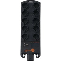
CR2050 - Schnittstelle IFM - Kostenlose Bedienungsanleitung
Finden Sie kostenlos die Bedienungsanleitung des Geräts CR2050 IFM als PDF.


Benutzerfragen zu CR2050 IFM
0 Frage zu diesem Gerät. Beantworten Sie die, die Sie kennen, oder stellen Sie Ihre eigene.
Eine neue Frage zu diesem Gerät stellen
Laden Sie die Anleitung für Ihr Schnittstelle kostenlos im PDF-Format! Finden Sie Ihr Handbuch CR2050 - IFM und nehmen Sie Ihr elektronisches Gerät wieder in die Hand. Auf dieser Seite sind alle Dokumente veröffentlicht, die für die Verwendung Ihres Geräts notwendig sind. CR2050 von der Marke IFM.
BEDIENUNGSANLEITUNG CR2050 IFM
CE
Betriebsanleitung
ioControl
CR2050
CR2051
CR2052

Inhalt
1 Vorbemerkung 4
1.1 Zeichenerklärung 4
2 Sicherheitshinweise 5
3 Bestimmungsgemäße Verwendung 6
4 Funktion 7
5 Montage 7
5.1 Montageort 7
5.2 Montagefläche 7
5.3 Wärmeabführung 8
5.4 Befestigung 8
5.5 Kabeldichtung....9
6 Elektrischer Anschluss 9
6.1 Anschlussbelegung 9
6.2 Generelle Anschlusshinweise.... 10
6.3 Anschlusstechnik 10
6.4 Anschlusszubehör 11
6.5 Frequenzeingänge 11
6.6 Verpolungsschutz....11
6.7 Versorgung der Signalgeber an den Eingängen .....11
6.8 Sicherungen 12
6.9 Beispiele für Anschlussarten 13
6.9.1 CR2050 13
6.9.2 CR2051 14
6.9.3 CR2052 15
7 Bedien- und Anzeigeelemente 16
7.1 Menüstruktur 17
7.2 Statusanzeige der Eingänge/Ausgänge (I/O-LEDs, gelb) 18
8 Inbetriebnahme.... 19
8.1 E/A-Modul.... 19
8.1.1 Anzeigemodus 19
8.1.2 Parametrierung 20
8.1.3 Parameterliste 21
8.2 Controller 21
8.2.1 Programmierung 21
8.3 Benötigte Dokumentationen.... 21
8.4 Benötigte Hardware 22
9 Technische Daten 23
9.1 CR2050 23
9.2 CR2051 30
9.3 CR2052 37
10 Wartung, Instandsetzung und Entsorgung 45
11 Zulassungen/Normen 45
12 Appendix.... 46
12.1 EMCY Object 46
12.2 Object directory CR205x 47
12.2.1 Device-specific CR2050.... 50
12.2.2 Device-specific CR2051....71
12.2.3 Device-specific CR2052....95
12.3 SDOs error messages 127
12.3.1 CR2050 127
12.3.2 CR2051 129
12.3.3 CR2052 131
1 Vorbemerkung
Technische Daten, Zulassungen, Zubehör und weitere Informationen unter www.ifm.com.
1.1 Zeichenerklärung
▶ Handlungsanweisung
▷ Reaktion, Ergebnis
[...] Bezeichnung von Tasten, Schaltflächen oder Anzeigen
→ Querverweis
Wichtiger Hinweis
Fehlfunktionen oder Störungen sind bei Nichtbeachtung möglich.
Information
Ergänzender Hinweis

WARNUNG!
Warnung vor schweren Personenschäden.
Tod oder schwere irreversible Verletzungen sind möglich.

VORSICHT!
Warnung vor Personenschäden.
Leichte reversible Verletzungen sind möglich.
ACHTUNG!
Warnung vor Sachschäden.
2 Sicherheitshinweise
- Das beschriebene Gerät wird als Teilkomponente in einem System verbaut. Die Sicherheit dieses Systems liegt in der Verantwortung des Erstellers. Der Systemersteller ist verpflichtet, eine Risikobeurteilung durchzuführen und daraus eine Dokumentation nach den gesetzlichen und normativen Anforderungen für den Betreiber und den Benutzer des Systems zu erstellen und beizulegen. Diese muss alle erforderlichen Informationen und Sicherheitshinweise für den Betreiber, Benutzer und ggf. vom Systemersteller autorisiertes Servicepersonal beinhalten.
- Dieses Dokument vor Inbetriebnahme des Produktes lesen und während der Einsatzdauer aufbewahren.
- Das Produkt muss sich uneingeschränkt für die betreffenden Applikationen und Umgebungsbedingungen eignen.
- Das Produkt nur bestimmungsgemäß verwenden ( → 3 Bestimmungsgemäße Verwendung).
- Die Missachtung von Anwendungshinweisen oder technischen Angaben kann zu Sach- und / oder Personenschäden führen.
- Bei Fehlfunktionen des Geräts mit dem Hersteller in Verbindung setzen. Eingriffe in das Gerät sind nicht zulässig.
- Montage, elektrischer Anschluss, Inbetriebnahme, Programmierung, Konfiguration, Bedienung und Wartung des Produktes darf nur für die jeweilige Tätigkeit ausgebildetes, autorisiertes Fachpersonal durchführen.
- Geräte, Stecker und Kabel wirksam vor Beschädigung schützen.
- Beschädigte Geräte austauschen, da anderenfalls die technischen Daten und die Sicherheit beeinträchtigt werden.
ACHTUNG!
Überstrom, Schweißperlen und Verschmutzung durch Schweißarbeiten
▷ Beschädigung des Geräts, Beeinträchtigung der elektrischen Sicherheit
▶ Schweißarbeiten am Fahrgestellrahmen nur durch Fachpersonal vornehmen.
▶ Plus- und Minusklemmen der Batterien abnehmen und abdecken.
▶ Gerät vor dem Schweißen am Fahrzeug bzw. an der Anlage mit allen Kontakten vom Bordnetz trennen.
▶ Masseklemme des Schweißgerätes direkt mit dem zu schweißenden Teil verbinden.
▶ Gerät und elektrische Leitungen nicht mit der Schweißelektrode oder der Masseklemme des Schweißgerätes berühren.
▶ Gerät inkl. aller Anschlussstecker und alle Verbindungsleitungen gegen Schweißperlen und andere Verschmutzungen schützen.
3 Bestimmungsgemäße Verwendung
Die frei programmierbaren Steuerungen der Baureihe "ioControl" sind für den Einsatz unter erschwerten Bedingungen ausgelegt: Dazu gehören erweiterter Temperaturbereich, starke Vibrationen, intensive EMV-Belastung, nasse Umgebung.
Die Ein- und Ausgänge werden vom Anwender durch die Applikationssoftware auf die jeweiligen Einsatzfälle angepasst. Die Steuerungen können als CANopen-Device, Master oder intelligentes E/A-Modul eingesetzt werden ( → 9 Technische Daten).
In Verbindung mit zusätzlichen Produkten der modularen ioControl- und Basic-Baureihe sind applikationsspezifische Erweiterungen und Anpassungen möglich.

WARNUNG!
Beeinträchtigung der Sicherheitsfunktion
▷ Gefährdung von Anlagen und Personen möglich
Das Gerät ist nicht für sicherheitsrelevante Aufgaben im Sinne des Personenschutzes zugelassen.
▶ Das Gerät nur innerhalb der Grenzen der technischen Daten einsetzen ( → 9 Technische Daten).
4 Funktion
- Die Applikationssoftware kann vom Anwender mit dem IEC 61131-3 konformen Programmiersystem CODESYS 2.3 erstellt werden. Im Lieferungszustand sind die Geräte als CANopen-Device vorkonfiguriert.
• 2 CAN Schnittstellen - Konfigurierbare Ein-/Ausgänge
- Status-LEDs, I/O-LEDs und 4-stellige 10-Segment-Anzeige
- Bedientasten
Weitere Informationen und Zubehör unter www.ifm.com.
5 Montage
5.1 Montageort
Folgende Montageorte sind zulässig:
• Kabineninnenbereich
- Karosserie
- Fahrzeugrahmen
Die Montage am Motor ist nicht zulässig.
Für den nicht mobilen Einsatz sind die gültigen Vorschriften unter Berücksichtigung der spezifizierten Umgebungsbedingungen einzuhalten.
5.2 Montagefläche

Auf das Gehäuse dürfen keine Verwindungskräfte oder mechanischen Belastungen wirken.
▶ Das Gerät auf einer ebenen Fläche montieren. Geeignete Ausgleichelemente verwenden.

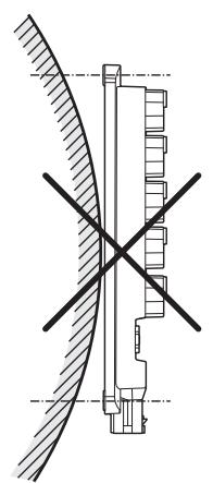
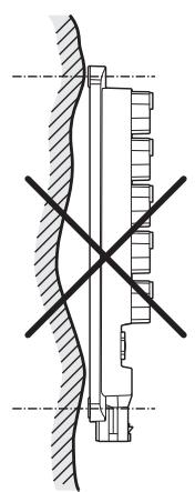

Montagefläche
5.3 Wärmeabführung

VORSICHT!
Das Gehäuse kann sich stark erwärmen.
▷ Verbrennungsgefahr.
▶ Bei Montage für ausreichende Wärmeabführung sorgen.
▶ Maximale Geräteerwärmung im Einsatzbereich messen. Die im Datenblatt angegebene Gehäusetemperatur darf nicht überschritten werden.
Bei Erreichen personengefährdender Gehäusetemperaturen:
▶ Gehäuse gegen unbeabsichtigtes Berühren schützen.
▶ Warnhinweis für heiße Oberflächen am Gerät sichtbar aufbringen.
5.4 Befestigung
▶ Die beiliegenden Rohrnieten von der Geräterückseite in die 3 Befestigungslöcher setzen.
▶ Das Gerät mit 3 Unterlegscheiben und M5 Schrauben befestigen. Die Schrauben dabei wechselweise anziehen.
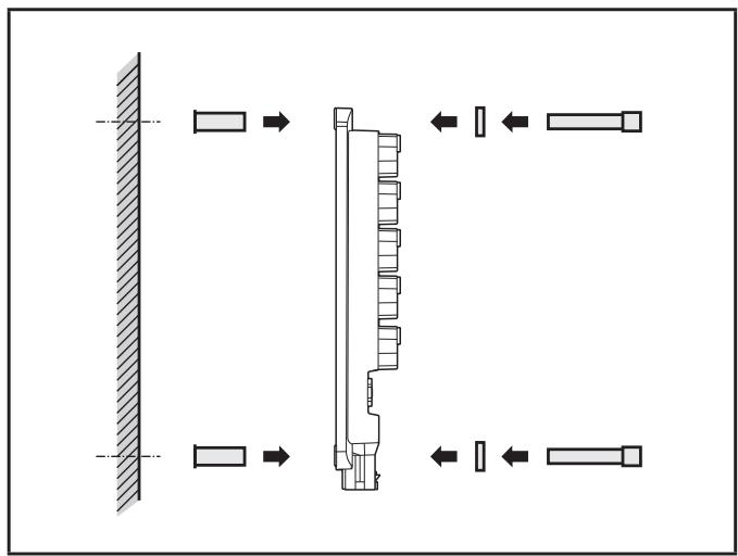

Einsetzen der Rohrnieten
Anzugdrehmoment: 2,0 Nm Bohrmaße ( → 9 Technische Daten)
| Verwendbare Schrauben (Beispiele): | Norm |
| Zylinderschrauben mit Innensechskant (M5 x L) | DIN EN ISO 4762 |
| Zylinderschrauben mit Innensechskant und niedrigem Kopf (M5 x L) | DIN 7984 |
5.5 Kabeldichtung

Vor und während der Montage Verschmutzungsgrad einhalten ( → 9 Technische Daten), bis Schutzart durch Stecker / Blindstopfen sicher-gestellt ist. Schutzart IP 65 / IP 67 ist nur gewährleistet, wenn alle Steckplätze durch Stecker oder durch Blindstecker abgedichtet werden.
▶ Bei starker Feuchtigkeit Gerät nur an senkrechter Fläche montieren.

Bei erhöhten Umweltanforderungen an die Module wird die Verwendung von Steckern mit der Dichtgeometrie der „enhanced seal retention“-Serie der Firma Deutsch oder Amphenol empfohlen.

Am Boden des Gerätes können unterschiedlich breite Spaltmaße vorhanden sein. Diese beeinflussen die Funktionen des Geräts nicht.
6 Elektrischer Anschluss

▶ Vor Anschluss des Geräts die Anlage spannungsfrei schalten, ggf. auch unabhängig versorgte Ein-/Ausgangslastkreise.
▶ Nationale und internationale Vorschriften zur Errichtung elektrotechnischer Anlagen befolgen.
▶ Anforderungen der Norm IEC 60204 berücksichtigen.
Berührbare Oberflächen des Geräts sind zu den Stromkreisen isoliert mit Basisisolierung nach IEC 61010-1 (Sekundärstromkreis mit max. 32 V DC, abgeleitet von Netzstromkreis bis 300 V der Überspannungskategorie II).
Die externe Verdrahtung muss die jeweils erforderliche Trennung zu anderen Stromkreisen sicherstellen.
6.1 Anschlussbelegung
Anschlussbelegung ( → 9 Technische Daten)

An den Anschlussklemmen dürfen nur die in den technischen Daten / auf dem Geräteaufdruck angegebenen Signale eingespeist bzw. die zugelassenen Zubehörkomponenten der ifm electronic gmbh angeschlossen werden.

Das Gerät ist für die Versorgung durch ein mobiles Bordnetz (12/24 V DC Nennspannung) oder SELV/PELV gemäß der technischen Daten und nationalen Vorschriften ausgelegt. Die Versorgung wird direkt ohne galvanische Trennung an die angeschlossenen Sensoren/Aktuatoren weitergeleitet.
6.2 Generelle Anschlusshinweise
Die Anschlüsse der Versorgungsleitungen und der CAN2-Schnittstelle erfolgen über den Stecker X1 an der Geräteunterseite. Die Anschlüsse der Ein-/Ausgänge, der CAN1-Schnittstelle und der CAN-Versorgung erfolgen über die Deutsch-Stecker auf der Gehäusefrontseite.
Anschlussbelegung ( → 9 Technische Daten)
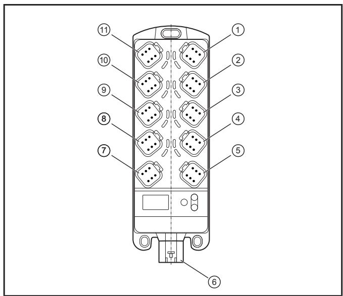
Steckerfeld
1: Anschluss 8
2: Anschluss 6
3: Anschluss 4
4: Anschluss 2
5: CAN1 OUT
6: X1 - Anschluss Leistungsstecker
7: CAN1 IN
8: Anschluss 1
9: Anschluss 3
10: Anschluss 5
11: Anschluss 7
| Anschluss | CR2050 | CR2051 | CR2052 | Polzahl |
| 1 | IN00 / IN08 | OUT00 / OUT08 | IN00 / IN04 | 6 |
| 2 | IN01 / IN09 | OUT01 / OUT09 | OUT00 / OUT04 | 6 |
| 3 | IN02 / IN10 | OUT02 / OUT10 | IN01 / IN05 | 6 |
| 4 | IN03 / IN11 | OUT03 / OUT11 | OUT01 / OUT05 | 6 |
| 5 | IN04 / IN12 | OUT04 / OUT12 | IN02 / IN06 | 6 |
| 6 | IN05 / IN13 | OUT05 / OUT13 | OUT02 / OUT06 | 6 |
| 7 | IN06 / IN14 | OUT06 / OUT14 | IN03 / IN07 | 6 |
| 8 | IN07 / IN15 | OUT07 / OUT15 | OUT03 / OUT07 | 6 |
| CAN1 IN | CAN1-Schnittstelle | 6 | ||
| CAN1 OUT | CAN1-Schnittstelle (z. B. zum Durchschleifen) | 6 | ||
| X1 | Versorgungsspannung und CAN2-Schnittstelle | 6 | ||

Falscher Anschluss kann zur Beschädigung des Gerätes führen.
▶ Sicherheitshinweise beachten ( → 2).
6.3 Anschlusstechnik
▶ Grundsätzlich alle ▶ Versorgungs- und Signalleitungen getrennt führen.
▶ Versorgungs- und Signalleitungen auf kürzestem Weg vom Gerät wegführen.
▶ Geräteaufdruck beachten.
▶ Für den CAN-Anschluss paarig verdrillte Leitungen verwenden.
▶ Alle abgehenden Kabel nach 400 mm mit einer geeigneten Zugentlastung versehen.
▶ Nicht belegte Buchsen mit Blindsteckern versehen.
6.4 Anschlusszubehör
Informationen zum verfügbaren Zubehör unter www.ifm.com
6.5 Frequenzeingänge
CR2050 / CR2052:
▶ Frequenzeingänge mit geschirmten Leitungen betreiben, damit Nutzsignale nicht durch Fremdstörungen beeinflusst werden.
6.6 Verpolungsschutz
ACHTUNG!
Fehlender Verpolungsschutz
Verpolungsschutz besteht nur bei Versorgung durch Bordnetz (mit Batterie), wenn diese Versorgung gesamthaft verpolt wird (Batterie falsch angeschlossen). Der Verpolungsschutz beruht darauf, dass im Fall der Verpolung die vorgeschalteten Sicherungen durch Überstrom schnell abschalten. Bei Versorgung durch SELV/PELV ist der Verpolungsschutz nicht gewährleistet.
▷ Beschädigung des Geräts Brandgefahr möglich
▶ Korrekten Anschluss der Kabelenden am Stecker vor deren Montage am Gerät sicherstellen, auch bei Bordnetzbetrieb.
CR2051: Ein Schutz gegen Verpolung der CAN-Versorgungsspannung ist nicht gegeben, da diese Spannung innerhalb des Gerätes nicht verwendet wird.
6.7 Versorgung der Signalgeber an den Eingängen
CR2050 / CR2052:
▶ Als Versorgungsspannung für die Signalgeber an den Eingängen (z. B. Schalter oder Sensoren) die Sensorspannung VBBs des entsprechenden Anschlusssteckers verwenden.
▶ Wenn der Eingang (Schalter oder Sensor) über eine externe Spannung versorgt wird, diese mit max. 3 A absichern.
6.8 Sicherungen
▶ Zum Schutz des gesamten Systems die einzelnen ▶ Stromkreise absichern.
| Bezeichnung | Potential | Stecker: Pin | Sicherung | |
| VBBS | Versorgung Sensorik/Modul | 8...32 V DC | AMP-Anschlussstecker: Pin 4 | CR2050: 3 ACR2052: 3 Aeforderliche Auslösecharakteristik:Tfuse ≤ 120 s bei max. 6,25 A |
| VBB1 | Versorgung AusgängeCR2050: nicht vorhandenCR2051: OUT00, 02, 04, 06, 08, 10, 12, 14CR2052: nicht vorhanden | 8...32 V DC | AMP-Anschlussstecker: Pin 4 | CR2050: -CR2051: ≤ 25 ACR2052: - |
| VBB2 | Versorgung AusgängeCR2050: nicht vorhandenCR2051: OUT01, 03, 05, 07, 09, 11, 13, 15CR2052: OUT00...07 | 8...32 V DC | AMP-Anschlussstecker: Pin 6 | CR2050: -CR2051: ≤ 25 ACR2052: ≤ 25 A |
| VCAN | Optionale Versorgung CAN1-SchnittstelleCR2050: verbunden mit VBBS CR2051: keine Verbindungmit VBBS CR2052: verbunden mit VBBS | 8...32 V DC | CAN IN: Pin3 + 4 | CR2050: -CR2051: 3 ACR2052: -erforderliche Auslösecharakteristik:Tfuse ≤ 120 s bei max. 6,25 A |
▶ Die zu den Versorgungsspannungen gehörenden Masse-Pins (GND 1 , GND 2 , ggf. GND CAN ) mit der gemeinsamen Masse verbinden.

Die angegebene Auslösecharakteristik ist einzuhalten. Anderenfalls kann der Brandschutz beeinträchtigt sein.

VORSICHT!
Eingangsstrom ist nicht begrenzt.
▷ Kein Brandschutz
▶ Stromkreise absichern.
6.9 Beispiele für Anschlussarten
6.9.1 CR2050

6.9.2 CR2051
Ein Schutz gegen Überspannung aus dem KFZ-Bordnetz ist nur gegeben, wenn der Anschluss VBBs/VBB1 mit mindestens 15 A abgesichert wird (Beispiel 3) oder wenn alle Spannungen über eine gemeinsame Sicherung abgesichert werden (Beispiele 1 und 2).
6.9.3 CR2052
Ein Schutz gegen Überspannung aus dem KFZ-Bordnetz ist nur gegeben, wenn der Anschluss VBB 2 mit mindestens 15 A abgesichert wird (Beispiel 3) oder wenn alle Spannungen über eine gemeinsame Sicherung abgesichert werden (Beispiele 1 und 2).
7 Bedien- und Anzeigeelemente
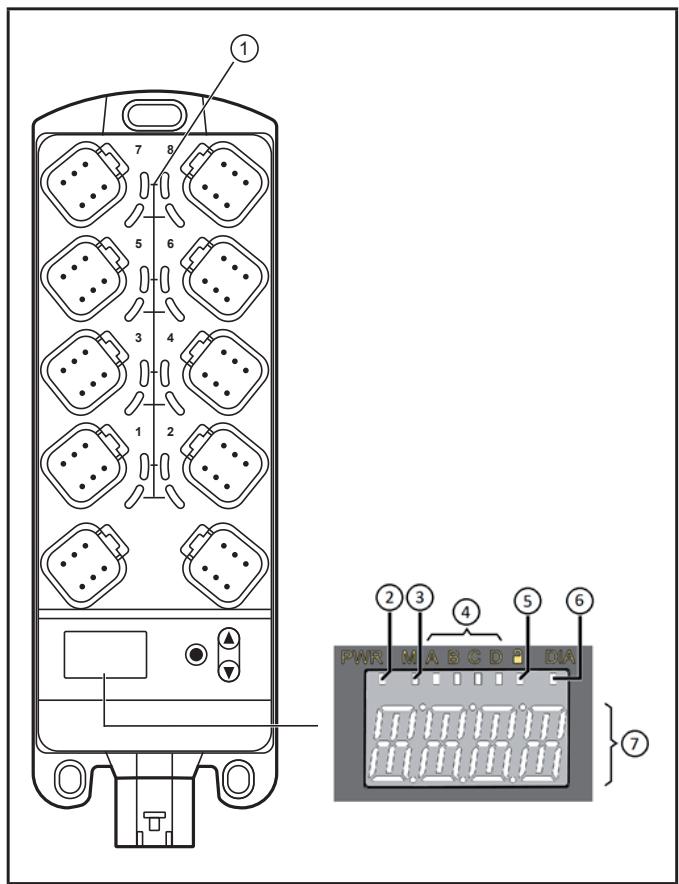
Anzeigeelemente
1: I/O-LEDs (gelb)
2: Power-LED (grün)
3: Mode-LED (grün)
4: Applikations-LEDs LED A... LED D (grün)
5: Lock-LED (grün)
6: Diagnose-LED (rot)
7: 4-stellige 10-Segment-Anzeige
10 -Segment-Anzeige ( → 9 Technische Daten)

Bedienelemente
1: Taste UP
2: Taste DOWN
3: Taste ENTER
Tastenfunktionen ( → 8.1 E/A-Modul).

Bedienelemente für Handbedienung!
Bedienung insbesondere mit spitzen Werkzeugen ist nicht zulässig. Die Tasten können dadurch beschädigt werden, wodurch die Schutzart nicht mehr eingehalten wird.

An der Anzeige können Helligkeitsunterschiede vorkommen.
7.1 Menüstruktur

Die folgende Beschreibung der Menüstruktur bezieht sich auf den Auslieferzustand des Geräts als E/A-Modul. Wenn das Gerät als Controller eingerichtet wird, muss eine entsprechende Menüstruktur definiert werden (siehe Systemhandbuch ioControl).
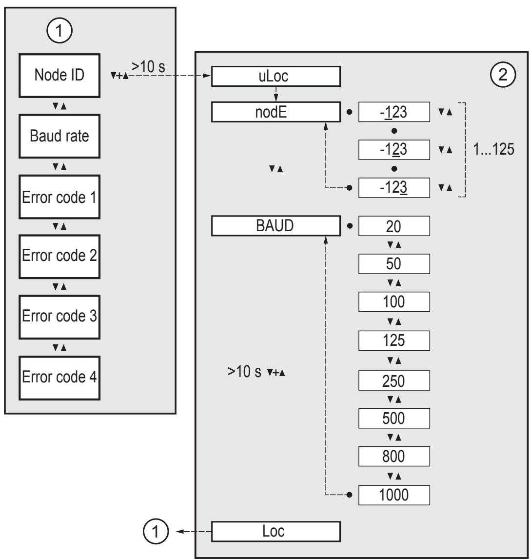
1: Anzeigemodus ( → 8.1.1)
2: Editiermodus ( → 8.1.2)
Parameterliste: (→ 8.1.3)
7.2 Statusanzeige der Eingänge/Ausgänge (I/O-LEDs, gelb)
| I/O-Konfiguration(siehe Objektverzeichnis im Anhang) | LED-Zustand | Beschreibung |
| 0 (nicht benutzt) | Aus | |
| 1 (Digitaleingang BL ) | Aus | Eingangssignal FALSE |
| Ein | Eingangssignal TRUE | |
| 2 (Digitalausgang BH ) | Aus | Ausgangssignal FALSE |
| Ein | Ausgangssignal TRUE | |
| 3 (Spannungseingang 10 V) | Aus | |
| 4 (PWM-Ausgang) | Aus | PWM-Wert = 0 ‰ |
| Ein | PWM-Wert > 0 ‰ | |
| 5 (Stromgeregelter Ausgang) | Aus | Stromwert ≤ 70 mA |
| Ein | Stromwert > 70 mA | |
| 6 (Spannungseingang 32 V, ratiometrisch) | Aus | |
| 7 (Stromeingang 20 mA) | Aus | |
| 2 Hz | Fehler am Eingang | |
| 9 (Spannungseingang 32 V) | Aus | |
| 10 (Digitaleingang BL ) | Aus | Eingangssignal FALSE |
| Ein | Eingangssignal TRUE | |
| 11 (Digitaleingang BL , mit Diagnose) | Aus | Eingangssignal FALSE |
| Ein | Eingangssignal TRUE | |
| 2 Hz | Fehler am Eingang | |
| 12 (Digitaleingang BH ) | Aus | Eingangssignal FALSE |
| Ein | Eingangssignal TRUE | |
| 14 (Frequenzeingang) | Aus | |
| 2 Hz | Fehler am Eingang | |
| 15 (Digitalausgang BH , mit Diagnose) | Aus | Ausgangssignal FALSE |
| Ein | Ausgangssignal TRUE | |
| 2 Hz | Fehler am Ausgang | |
| 16 (Digitalausgang BH , mit Diagnose,kurzschluss- und überlastfest) | Aus | Ausgangssignal FALSE |
| Ein | Ausgangssignal TRUE | |
| 2 Hz | Fehler am Ausgang | |
| 18 (Widerstandseingang) | Aus | |
| 2 Hz | Fehler am Eingang | |
| 20 (Periodendauermessung) | Aus | |
| 2 Hz | Fehler am Eingang |
8 Inbetriebnahme
8.1 E/A-Modul
Im Auslieferzustand ist das Gerät als E/A-Modul konfiguriert.
Nach dem Einschalten zeigt die 10-Segment-Anzeige die Artikelnummer des Geräts und danach die eingestellte Node-ID an.
8.1.1 Anzeigemodus
Leuchtet die grüne Lock-LED, befindet sich das Gerät im Anzeigemodus. Das Gerät kann nur die eingestellte Node-ID und Baudrate sowie ggf. vorliegende Fehlermeldungen anzeigen; ▷ Parameter können nicht editiert werden.
▶ Taste DOWN drücken.
▷ Gerät zeigt eingestellte Baudrate an.
▶ Taste DOWN drücken.
▷ Gerät zeigt Fehlercode 1 an, sofern vorhanden.
▶ Taste DOWN erneut drücken.
▶ Mit Taste UP zurück.▷ Gerät zeigt bei jedem Tastendruck DOWN einen weiteren Fehlercode an, sofern vorhanden.
Maximal 4 verschiedene Fehlercodes können vorliegen und angezeigt werden:
| Fehlercode | Beschreibung |
| UBB2 | keine Versorgungsspannung |
| SH | Kurzschluss gegen GND |
| OP | Leiterbruch |
| LF | Frequenzeingang, Frequenz zu niedrig |
| oC | Stromeingang, Strom zu hoch |
| oL | Überstrom |
| IP | falsche Parametrierung |
| Comm | Kommunikationsfehler |
| HrTB | Heart Beat Error |
| mEmr | Speicherfehler |
| SYnC | Synchronisationsfehler |
Nach 10 s ohne Tastenbedienung zeigt das Gerät die eingestellte Node-ID an.
8.1.2 Parametrierung
▶ Tasten UP und DOWN gleichzeitig min. 10 s drücken, um in den Editiermodus zu wechseln.
▷ Grüne Lock-LED erlischt.
▷ Parameter können editiert werden.
▷ Anzeige "uLoc" für 5 s
▷ Anzeige "nodE"
▶ Taste ENTER drücken.
▷ Gerät zeigt eingestellte Node-ID an.
▷ Die 1. editierbare Ziffer blinkt.
▶ Mit den Tasten UP und DOWN den gewünschten Wert einstellen.
▶ Mit der Taste ENTER zur nächsten Ziffer springen.
▷ Die 2. editierbare Ziffer blinkt.
▶ Mit den Tasten UP und DOWN den gewünschten Wert einstellen.
▶ Mit der Taste ENTER zur nächsten Ziffer springen.
▷ Die 3. editierbare Ziffer blinkt.
▶ Mit den Tasten UP und DOWN den gewünschten Wert einstellen.
▶ Taste ENTER drücken.
▷ Eingestellte Node-ID wird übernommen.
▷ Anzeige "nodE"
▶ Taste DOWN drücken.
▷ Anzeige "BAUD"
▶ Taste ENTER drücken.
▷ Gerät zeigt eingestellte Baudrate an.
▶ Mit den Tasten UP und DOWN den gewünschten Wert einstellen.
▶ Taste ENTER drücken.
▷ Eingestellte Baudrate wird übernommen.

Änderungen der Parameter werden erst nach einem Reset des Geräts wirksam.
Editiermodus beenden:
▶ Tasten UP und DOWN gleichzeitig min. 10 s drücken.
▷ Grüne Lock-LED an.
Parameter können nicht editiert werden.▷ Anzeige "Loc" für 5 s, danach Anzeige der eingestellten Node-ID

Nach 30 s ohne Tastaturbedienung beendet das Gerät den Editiermodus automatisch.
8.1.3 Parameterliste
| Parameter | Funktion | Wertebereich | Defaultwert |
| nodE | Node-ID des Geräts | 1...125 | 125 |
| BAUD | Baudrate | 20, 50, 100, 125, 250, 500, 800, 1000 kBit/s | 250 kBit/s |
8.2 Controller
Das Gerät kann als Controller konfiguriert werden. Dadurch verliert es die bisherige Menüstruktur sowie die Eigenschaften als E/A-Modul.
8.2.1 Programmierung
Die Applikationssoftware kann vom Anwender mit dem IEC 61131-3 konformen Programmiersystem CODESYS 2.3 erstellt werden.

Für die sichere Funktion der vom Anwender erstellten Applikationsprogramme ist dieser selbst verantwortlich. Bei Bedarf muss er entsprechend der nationalen Vorschriften zusätzlich eine Abnahme durch entsprechende Prüf- und Überwachungsorganisationen durchführen lassen.

Hinweise zur Einstellung der CAN-ID und der Baudrate bei Verwendung als CANopen-Device finden Sie im Systemhandbuch.
8.3 Benötigte Dokumentationen
Neben dem Programmiersystem CODESYS V2.3 werden zur Inbetriebnahme und Programmierung des Gerätes folgende Dokumente benötigt:
- Programmierhandbuch CODESYS V2.3
• Systemhandbuch ioControl
Als Download-File stehen die Handbücher im Internet zur Verfügung: www.ifm.com
8.4 Benötigte Hardware
Bei Verwendung als Mobilsteuerung ist zum Laden des Applikationsprogramms in das Gerät ein CAN-Interface für den Anschluss an einen PC oder ein Notebook erforderlich.
Beispiel:
• CAN/RS232-USB Interface CANfox (EC2112)
- Adapterkabel für CANfox (EC2113)
Informationen zum verfügbaren Zubehör unter:
www.ifm.com
9 Technische Daten
9.1 CR2050
CR2050
E/A-Modul
digital und analog
für System R360
CANopen Device
Mobilsteuerung
Programmierung
nach IEC 61131-3
16 Eingänge
2 CAN-Schnittstellen
8...32 V DC
CE


1: Taste ENTER
2: Tasten UP/DOWN
3: 10-Segment-Anzeige
4: DEUTSCH-Stecker
5: AMP-Anschlussstecker
Technische Daten
Mechanische Daten
Gehäuse
Abmessungen (H x B x T)
Montage
Anschluss
Eingänge
CAN1-Schnittstelle
Betriebsspannung, CAN2
Schutzart
Betriebs-/Lagertemperatur
Max. zulässige relative Luftfeuchtigkeit
Max. Höhe über NN
Verschmutzungsgrad
Gewicht
Elektrische Daten
Betriebsspannung
Stromaufnahme
Überspannung
Unterspannungserkennung
Unterspannungsabschaltung
Prozessor
Speicher (gesamt)
Speicheraufteilung
Modulares Steuerungssystem Einsetzbar als CANopen-Device oder intelligentes E/A-Modul
| Gehäuse: PA6/6.6 Anzeigefenster: PATasten: Silikon |
| 234 x 76 x 40,5 mm (ohne Rohrniete) |
| Befestigung mit 3 Schrauben M5 nach DIN EN ISO 4762 oder DIN 7984, 3 Rohrnieten nach DIN 7340 und 3 Unterlegscheiben nach DIN EN ISO 7092 (Rohrniete und Unterlegscheiben liegen bei) |
| Versorgung: MCP2.8 6 polig für Stecker TE-AMP 1745078-1 Ein-/Ausgänge: Deutsch DT04-6S 6 polig Kontakte: AMP: CuFe verzinnt; Deutsch: CuZn vergoldet |
8 x 6-polig
2 x 6-polig
1 x 6-polig
IP 65 und IP 67 (alle Stecker gesteckt)
-40...85°C / -40...85°C
90 %, nicht kondensierend
2000 m
2
450 g
8...32 V DC
100 mA (bei 24 V DC) / 185 mA (bei 12 V DC) / max. 300 mA
36 V für t ≤ 10 s
bei UB ≤ 7,8 V
bei UB ≤ 7,0 V
Freescale PowerPC, 50 MHz
592 kByte RAM / 1536 kByte Flash / 1 kByte FRAM
siehe Programmierhandbuch ioControl und www.ifm.com
CR2050
Geräteüberwachung
CAN Schnittstellen 1 und 2
Baudrate
Kommunikationsprofil
Software/Programmierung
Programmiersystem
Eingänge
Konfigurationen
Anzeigeelemente
I/O-LEDs
Power-LED (PWR)
Mode-LED (M)
Applications-LEDs (A... D)
Lock-LED (Schloss-Symbol)
Diagnose-LED (DIA)
Anzeige
Betriebszustände bei Verwendung als Mobilsteuerung
Technische Daten
Unterspannungsüberwachung
Watchdogfunktion
Checksummenprüfung für Programm und System
Übertemperaturüberwachung
CAN Interface 2.0 A/B, ISO 11898
20 kBit/s...1 MBit/s (Default CAN1: 250 kBit/s, CAN2: 250 kBit/s)
CANopen, CiA DS 301 Version 4, CiA DS 401 Version 1.4
oder SAE J 1939 oder freies Protokoll
CODESYS Version 2.3 (IEC 61131-3)
16 (konfigurierbar)
| Anzahl | Ausführung | |
| 8 | digital für positive/negative Gebersignale analog (0...10/32 V DC, 0...20 mA, ratiometrisch) | BL/BH A |
| 4 | digital für positive Gebersignale Widerstandsmessung (0,016...30 kΩ) | BL R |
| 4 | digital für positive Gebersignale digital für negative Gebersignale* Frequenz (≤ 30 kHz) | BL BH FRQ |
* nicht im E/A-Modul (CANopen Device) verfügbar
16 x LED orange
(Voreinstellung: Statusanzeige des jeweiligen Eingangs)
LED grün
(Voreinstellung: Signalisieren des System-Status)
LED grün
(Voreinstellung: Signalisiert eine Anzeige der Node-ID)
4 x LED grün
1 x LED grün
(Voreinstellung: Verriegelung der eingestellten Parameter)
1 x LED rot
(Voreinstellung: Anzeigen eines Fehlers)
4-stellige 10-Segment-Anzeige (zweifarbig: rot / grün)
(Voreinstellung: Anzeige der Baudrate oder Node-ID)
| LED | Zustand | Beschreibung |
| - | konstant aus | keine Betriebsspannung |
| PWR + DIA | 1 x ein | Initialisierung oder Reset Checks |
| PWR | 5 Hz | kein Betriebssystem geladen |
| 2 Hz | Applikation läuft (RUN) | |
| konstant ein | Applikation angehalten (STOP) | |
| DIA | 10 Hz | Applikation angehalten (STOP mit Fehler) |
| 5 Hz | Applikation angehalten wegen Unterspannung | |
| konstant ein | System-Fehler (Fatal Error) |
CR2050
Bedienelemente
Tasten
Tasten (Voreinstellung)
Kennwerte der Eingänge
Analogeingänge (B L , B H , A)
IN00 - Anschluss 1, Pin 5
IN01 - Anschluss 2, Pin 5
IN02 - Anschluss 3, Pin 5
IN03 - Anschluss 4, Pin 5
IN04 - Anschluss 5, Pin 5
IN05 - Anschluss 6, Pin 5
IN06 - Anschluss 7, Pin 5
IN07 - Anschluss 8, Pin 5
konfigurierbar als...
Digitaleingänge (B L , R)
IN08 - Anschluss 1, Pin 2
IN10 - Anschluss 3, Pin 2
IN12 - Anschluss 5, Pin 2
IN14 - Anschluss 7, Pin 2
konfigurierbar als...
Technische Daten
ENTER, UP, DOWN
Einstellen der CAN-ID / Baudrate
| Spannungseingänge | |
| Eingangsspannung | 0...10 V oder 0...32 V |
| Auflösung | 12 Bit |
| Genauigkeit | ± 1% FS |
| Eingangswiderstand | 65,6 kΩ (0...10 V), 50,7 kΩ (0...32 V) |
| Eingangsfrequenz | ≤ 500 Hz |
| Stromeingänge, diagnosefähig | |
| Eingangsstrom | 0...20 mA |
| Auflösung | 12 Bit |
| Genauigkeit | ± 1% FS |
| Eingangswiderstand | 400 Ω |
| Eingangsfrequenz | ≤ 500 Hz |
| Bei Strömen > 23 mA wird der Eingang auf Spannungseingang umgeschaltet! | |
| Spannungseingänge, 0...32 V, ratiometrisch | |
| Funktion | (UIN ÷ UB) × 1000 ‰ |
| Wertebereich | 0...1000 ‰ |
| Eingangswiderstand | 50,7 kΩ |
| Binäre Spannungseingänge für positive Gebersignale | |
| Einschaltpegel | > 0,7 UB |
| Ausschaltpegel | < 0,3 UB |
| Eingangswiderstand | 3,2 kΩ |
| Eingangsfrequenz | 50 Hz |
| Diagnose Leiterbruch | > 0,95 UB |
| Diagnose Kurzschluss | < 1 V |
| Binäre Spannungseingänge für negative Gebersignale | |
| Einschaltpegel | > 0,7 UB |
| Ausschaltpegel | < 0,3 UB |
| Eingangswiderstand | 3,2 kΩ |
| Eingangsfrequenz | 50 Hz |
| ● Binäre Spannungseingänge für positive Gebersignale | |
| Einschaltpegel | >0,7 UB |
| Ausschaltpegel | <0,3 UB |
| Eingangswiderstand | 3,2 kΩ |
| Eingangsfrequenz | 50 Hz |
| Diagnose Leiterbruch | >0,95 UB |
| Diagnose Kurzschluss | <1 V |
| ● Widerstandseingang | |
| Messbereich | 0,016...30 kΩ |
| Genauigkeit | ± 2 % FS: 16 Ω...3 kΩ ± 5 % FS: 3...15 kΩ ± 10 % FS: 15...30 kΩ |
CR2050
Frequenzeingänge ( BL , BH , FRQ)
IN09 - Anschluss 2, Pin 2
IN11 - Anschluss 4, Pin 2
IN13 - Anschluss 6, Pin 2
IN15 - Anschluss 8, Pin 2
konfigurierbar als...
Max. Summenstrom der CAN-Versorgung + Sensorversorgungen VCAN + VBBS
Technische Daten
| • Frequenzeingänge | |
| Eingangswiderstand | 3,2 kΩ |
| Eingangsfrequenz | ≤ 30 kHz |
| Einschaltpegel | >0,7 UB |
| Ausschaltpegel | < 0,3 UB |
| • Binäre Spannungseingänge für positive Gebersignale | |
| Einschaltpegel | >0,7 UB |
| Ausschaltpegel | < 0,3 UB |
| Eingangswiderstand | 3,2 kΩ |
| Eingangsfrequenz | 50 Hz |
| Diagnose Leiterbruch* | >0,95 UB |
| Diagnose Kurzschluss* | < 1 V |
| • Binäre Spannungseingänge für negative Gebersignale* | |
| Einschaltpegel | >0,7 UB |
| Ausschaltpegel | < 0,3 UB |
| Eingangswiderstand | 3,2 kΩ |
| Eingangsfrequenz | 50 Hz |
* nicht im E/A-Modul (CANopen Device) verfügbar
1,5 A
| CR2050 | Technische Daten | |
| Prüfnormen und Bestimmungen | ||
| CE-Zeichen | EN 61000-6-2 | Elektromagnetische Verträglichkeit (EMV)Störfestigkeit |
| EN 61000-6-4 | Elektromagnetische Verträglichkeit (EMV)Störaussendung | |
| E1-Zeichen | UN/ECE-R10 | Störaussendung Störfestigkeit mit 100 V/m |
| ISO 7637-2 | Impuls 1, Schärfegrad: IV; Funktionszustand CImpuls 2a, Schärfegrad: IV; Funktionszustand AImpuls 2b, Schärfegrad: IV; Funktionszustand CImpuls 3a, Schärfegrad: IV; Funktionszustand AImpuls 3b, Schärfegrad: IV; Funktionszustand AImpuls 4, Schärfegrad: IV; Funktionszustand BImpuls 5, Schärfegrad: III; Funktionszustand C(Angaben gelten für 24 V System)Impuls 4, Schärfegrad: III; Funktionszustand C(Angabe gilt für 12 V System) | |
| Klimatische Prüfungen | EN 60068-2-30 | Feuchte Wärme zyklischobere Temperatur 55°C, Anzahl Zyklen: 6 |
| EN 60068-2-78 | Feuchte Wärme konstant Prüftemperatur 40°C / 93% RH,Prüfdauer: 21 Tage | |
| Mechanische Prüfungen | ISO 16750-3 | Test VII; Vibration, random Anbauort Karosserie |
| EN 60068-2-6 | Vibration, Sinus10...500 Hz; 0,72 mm/10 g; 10 Zyklen/Achse | |
| ISO 16750-3 | Dauerschocken30 g/6 ms; 24.000 Schocks | |
| Chemische Beständigkeit | ISO 16750-5:2010 | AA, BA, BD, CC, DB, DC, DDimmer nur eine Chemikalie gleichzeitig zulässig |
| Hinweis | EG-Konformitätserklärung und Zulassungen sind abrufbar unter:www.ifm.com | |
ifm electronic gmbh • Friedrichstraße 1 • 45128 Essen
Technische Änderungen behalten wir uns ohne Ankündigung vor!
CR2050 / Seite 5 04.12.2019
CR2050
Anschlussbelegung
Technische Daten
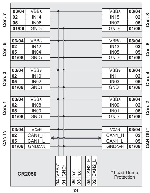
LED-Zuordnung
| Deutsch-Stecker | AMP-Stecker |
 | 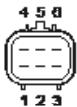 |
1: LED IN15
2: LED IN07
3: LED IN13
4: LED IN05
5: LED IN11
6: LED IN03
7: LED IN09
8: LED IN01
9: LED IN08
10: LED IN00
11: LED IN10
12: LED IN02
13: LED IN12
14: LED IN04
15: LED IN14
16: LED IN06
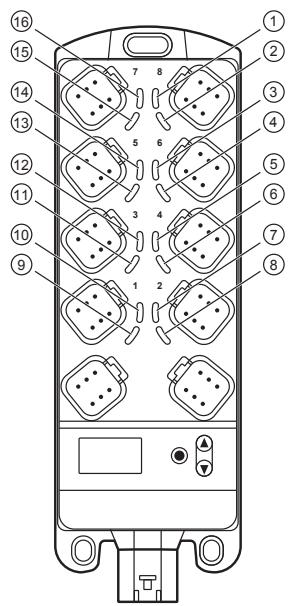
CR2050
Abkürzungen
Technische Daten
A Analog
BH Binär High-Side
BL Binär Low-Side
FRQ Frequenz-/Impulseingang
R Widerstandseingang
VBBs Versorgung Sensorik/Modul
VCAN Versorgung CAN-Stecker
9.2 CR2051
CR2051
E/A-Modul
digital und analog
für System R360
CANopen Device
Mobilsteuerung
Programmierung
nach IEC 61131-3
16 Ausgänge
2 CAN-Schnittstellen
8...32 V DC
CE

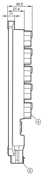

1: Taste ENTER
2: Tasten UP/DOWN
3: 10-Segment-Anzeige
4: DEUTSCH-Stecker
5: AMP-Anschlussstecker
Technische Daten
Mechanische Daten
Gehäuse
Abmessungen (H x B x T)
Montage
Anschluss
Ausgänge
CAN1-Schnittstelle
Betriebsspannung, CAN2
Schutzart
Betriebs-/Lagertemperatur
Max. zulässige relative Luftfeuchtigkeit
Max. Höhe über NN
Verschmutzungsgrad
Gewicht
Elektrische Daten
Betriebsspannung
Stromaufnahme
Überspannung
Unterspannungserkennung
Unterspannungsabschaltung
Prozessor
Speicher (gesamt)
Speicheraufteilung
Modulares Steuerungssystem
Einsetzbar als CANopen-Device oder intelligentes E/A-Modul
| Gehäuse: PA6/6.6 Anzeigefenster: PATasten: Silikon |
| 234 x 76 x 40,5 mm (ohne Rohrniete) |
| Befestigung mit 3 Schrauben M5 nach DIN EN ISO 4762 oder DIN 7984, 3 Rohrnieten nach DIN 7340 und 3 Unterlegscheiben nach DIN EN ISO 7092 (Rohrniete und Unterlegscheiben liegen bei) |
| Versorgung: MCP2.8 6 polig für Stecker TE-AMP 1745078-1 Ein-/Ausgänge: Deutsch DT04-6S 6 polig Kontakte: AMP: CuFe verzinnt; Deutsch: CuZn vergoldet |
8 x 6-polig
2 x 6-polig
1 x 6-polig
IP 65 und IP 67 (alle Stecker gesteckt)
-40...85°C / -40...85°C
90 %, nicht kondensierend
2000 m
2
450 g
8...32 V DC
104 mA (bei 24 V DC) / 185 mA (bei 12 V DC) / max. 300 mA
36 V für t ≤ 10 s
bei UB ≤ 7,8 V
bei UB ≤ 7,0 V
Freescale PowerPC, 50 MHz
592 kByte RAM / 1536 kByte Flash / 1 kByte FRAM
siehe Programmierhandbuch ioControl und
www.ifm.com
CR2051
Geräteüberwachung
CAN Schnittstellen 1 und 2
Baudrate
Kommunikationsprofil
Software/Programmierung
Programmiersystem
Ausgänge
Konfigurationen
Anzeigeelemente
I/O-LEDs
Power-LED (PWR)
Mode-LED (M)
Applications-LEDs (A... D)
Lock-LED (Schloss-Symbol)
Diagnose-LED (DIA)
Anzeige
Betriebszustände bei Verwendung als Mobilsteuerung
Technische Daten
Unterspannungsüberwachung
Watchdogfunktion
Checksummenprüfung für Programm und System
Übertemperaturüberwachung
CAN Interface 2.0 A/B, ISO 11898
20 kBit/s...1 MBit/s (Default CAN1: 250 kBit/s, CAN2: 250 kBit/s)
CANopen, CiA DS 301 Version 4, CiA DS 401 Version 1.4
oder SAE J 1939 oder freies Protokoll
CODESYS Version 2.3 (IEC 61131-3)
16 (konfigurierbar)
| Anzahl | Ausführung | |
| 4 | plusschaltend (High-Side), 4 A, Diagnose PWM-Ausgang (20...250 Hz), 4 A, Diagnose stromgeregelt 0,02...4 A | BH PWM PWMI |
| 4 | plusschaltend (High-Side), 2,5 A, Diagnose PWM-Ausgang (20...250 Hz), 2,5 A, Diagnose stromgeregelt 0,02...2,5 A | BH PWM PWMI |
| 4 | plusschaltend (High-Side), 4 A, Diagnose PWM-Ausgang (20...250 Hz), 4 A | BH PWM |
| 4 | plusschaltend (High-Side), 2,5 A, Diagnose PWM-Ausgang (20...250 Hz), 2,5 A | BH PWM |
16 x LED orange
(Voreinstellung: Statusanzeige des jeweiligen Ausgangs)
LED grün
(Voreinstellung: Signalisieren des System-Status)
LED grün
(Voreinstellung: Signalisiert eine Anzeige der Node-ID)
4 x LED grün
1 x LED grün
(Voreinstellung: Verriegelung der eingestellten Parameter)
1 x LED rot
(Voreinstellung: Anzeigen eines Fehlers)
4-stellige 10-Segment-Anzeige (zweifarbig: rot / grün)
(Voreinstellung: Anzeige der Baudrate oder Node-ID)
| LED | Zustand | Beschreibung |
| - | konstant aus | keine Betriebsspannung |
| PWR + DIA | 1 x ein | Initialisierung oder Reset Checks |
| PWR | 5 Hz | kein Betriebssystem geladen |
| 2 Hz | Applikation läuft (RUN) | |
| konstant ein | Applikation angehalten (STOP) | |
| DIA | 10 Hz | Applikation angehalten (STOP mit Fehler) |
| 5 Hz | Applikation angehalten wegen Unterspannung | |
| konstant ein | System-Fehler (Fatal Error) |
CR2051
Bedienelemente
Tasten
Tasten (Voreinstellung)
Kennwerte der Ausgänge
Digitalausgänge (B H , PWM, PWM I )
OUT00 - Anschluss 1, Pin 5
OUT01 - Anschluss 2, Pin 5
OUT02 - Anschluss 3, Pin 5
OUT03 - Anschluss 4, Pin 5
konfigurierbar als...
Digitalausgänge (B H , PWM, PWM I )
OUT04 - Anschluss 5, Pin 5
OUT05 - Anschluss 6, Pin 5
OUT06 - Anschluss 7, Pin 5
OUT07 - Anschluss 8, Pin 5
konfigurierbar als...
| Technische Daten |
| ENTER, UP, DOWN |
| Einstellen der CAN-ID / Baudrate |
| Halbleiterausgänge, plusschaltend (High-Side), kurzschluss- und überlastfest. Diagnose über Stromrücklesung (Leiterbruch / Überlast)Diagnose über Spannungsrücklesung, Pullup-Widerstand abschaltbar (Leiterbruch/Kurzschluss) | |
| Schaltspannung | 8...32 V |
| Schaltstrom | 0,02...4 A |
| Lastwiderstand | ≥ 3 Ω (bei 12 V DC) ≥ 6 Ω (bei 24 V DC) |
| Strommessbereich | 0,02...6 A |
| Genauigkeit Stromrücklesung | 1 % FS |
| PWM-Ausgänge | |
| Ausgangsfrequenz | 20...250 Hz |
| Tastverhältnis | 1...1000 ‰ |
| Schaltstrom | 0,02...4 A |
| Strommessbereich | 0,02...6 A |
| Genauigkeit Stromrücklesung | 3 % FS |
| Stromgeregelter Ausgang | |
| Ausgangsfrequenz | 20...250 Hz |
| Regelbereich | 0,02...4 A |
| Einstellauflösung | 1 mA |
| Max. Einschaltstrom | ≤ 24 A |
| Genauigkeit Stromrücklesung | 3 % FS |
| Halbleiterausgänge, plusschaltend (High-Side), kurzschluss- und überlastfest. Diagnose über Stromrücklesung (Leiterbruch / Überlast)Diagnose über Spannungsrücklesung, Pullup-Widerstand abschaltbar (Leiterbruch/Kurzschluss) | |
| Schaltspannung | 8...32 V |
| Schaltstrom | 0,02...2,5 A |
| Lastwiderstand | ≥ 4,8 Ω (bei 12 V DC) ≥ 9,6 Ω (bei 24 V DC) |
| Strommessbereich | 0,02...4 A |
| Genauigkeit Stromrücklesung | 1 % FS |
| PWM-Ausgänge | |
| Ausgangsfrequenz | 20...250 Hz |
| Tastverhältnis | 1...1000 ‰ |
| Schaltstrom | 0,02...2,5 A |
| Strommessbereich | 0,02...4 A |
| Genauigkeit Stromrücklesung | 3 % FS |
| Stromgeregelter Ausgang | |
| Ausgangsfrequenz | 20...250 Hz |
| Regelbereich | 0,02...2,5 A |
| Einstellauflösung | 1 mA |
| Max. Einschaltstrom | ≤ 24 A |
| Genauigkeit Stromrücklesung | 3 % FS |
CR2051
Digitalausgänge (B H , PWM)
OUT08 - Anschluss 1, Pin 2
OUT09 - Anschluss 2, Pin 2
OUT10 - Anschluss 3, Pin 2
OUT11 - Anschluss 4, Pin 2
konfigurierbar als...
Digitalausgänge (B H , PWM)
OUT12 - Anschluss 5, Pin 2
OUT13 - Anschluss 6, Pin 2
OUT14 - Anschluss 7, Pin 2
OUT15 - Anschluss 8, Pin 2
konfigurierbar als...
Freilaufdioden
Überlastfestigkeit
(Gültig für alle Ausgänge)
Kurzschlussfestigkeit
(gültig für alle Ein- und Ausgänge)
Max. Summenstrom der CAN-Versorgung VCAN
Max. Summenstrom der
Ausgangsversorgungen VBB 1 / VBB 2
(Dauerstrombelastung)
Technische Daten
- Halbleiterausgänge, plusschaltend (High-Side), kurzschluss- und überlastfest.
Diagnose über Spannungsrücklesung, Pullup-Widerstand abschaltbar (Leiterbruch/Kurzschluss)
| Schaltspannung | 8...32 V |
| Schaltstrom | 0,02...2,5 A |
| • PWM-Ausgänge | |
| Ausgangsfrequenz | 20...250 Hz |
| Tastverhältnis | 1...1000 ‰ |
| Schaltstrom | 0,02...2,5 A |
| Max. Einschaltstrom | ≤ 24 A |
- Halbleiterausgänge, plusschaltend (High-Side), kurzschluss- und überlastfest.
Diagnose über Spannungsrücklesung, Pullup-Widerstand abschaltbar (Leiterbruch/Kurzschluss)
| Schaltspannung | 8...32 V |
| Schaltstrom | 0,02...4 A |
| • PWM-Ausgänge | |
| Ausgangsfrequenz | 20...250 Hz |
| Tastverhältnis | 1...1000 ‰ |
| Schaltstrom | 0,02...4 A |
| Max. Einschaltstrom | ≤ 24 A |
Freilaufdioden zur Abschaltung induktiver Lasten sind integriert
≤ 5 Minuten (bei 100% Überlast)
≤ 5 Minuten
1,5 A

1: Montage Fahrzeug im Außenbereich (externe Konvektion)
2: Montage im Schaltschrank auf Metallplatte
3: Montage auf schlecht wärmeleitfähigem Untergrund (z. B. Kuststoff oder Holz)
| CR2051 | Technische Daten | |
| Prüfnormen und Bestimmungen | ||
| CE-Zeichen | EN 61000-6-2 | Elektromagnetische Verträglichkeit (EMV)Störfestigkeit |
| EN 61000-6-4 | Elektromagnetische Verträglichkeit (EMV)Störaussendung | |
| E1-Zeichen | UN/ECE-R10 | Störaussendung Störfestigkeit mit 100 V/m |
| ISO 7637-2 | Impuls 1, Schärfegrad: IV; Funktionszustand CImpuls 2a, Schärfegrad: IV; Funktionszustand AImpuls 2b, Schärfegrad: IV; Funktionszustand CImpuls 3a, Schärfegrad: IV; Funktionszustand AImpuls 3b, Schärfegrad: IV; Funktionszustand AImpuls 4, Schärfegrad: IV; Funktionszustand BImpuls 5, Schärfegrad: III; Funktionszustand C(Angaben gelten für 24 V System)Impuls 4, Schärfegrad: III; Funktionszustand C(Angabe gilt für 12 V System) | |
| Klimatische Prüfungen | EN 60068-2-30 | Feuchte Wärme zyklischobere Temperatur 55°C, Anzahl Zyklen: 6 |
| EN 60068-2-78 | Feuchte Wärme konstant Prüftemperatur 40°C / 93% RH,Prüfdauer: 21 Tage | |
| Mechanische Prüfungen | ISO 16750-3 | Test VII; Vibration, random Anbauort Karosserie |
| EN 60068-2-6 | Vibration, Sinus10...500 Hz; 0,72 mm/10 g; 10 Zyklen/Achse | |
| ISO 16750-3 | Dauerschocken30 g/6 ms; 24.000 Schocks | |
| Chemische Beständigkeit | ISO 16750-5:2010 | AA, BA, BD, CC, DB, DC, DDimmer nur eine Chemikalie gleichzeitig zulässig |
| Hinweis | EG-Konformitätserklärung und Zulassungen sind abrufbar unter:www.ifm.com | |
CR2051
Anschlussbelegung
Technische Daten

LED-Zuordnung
| Deutsch-Stecker | AMP-Stecker |
 | 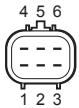 |
1: LED OUT15
2: LED OUT07
3: LED OUT13
4: LED OUT05
5: LED OUT11
6: LED OUT03
7: LED OUT09
8: LED OUT01
9: LED OUT08
10: LED OUT00
11: LED OUT10
12: LED OUT02
13: LED OUT12
14: LED OUT04
15: LED OUT14
16: LED OUT06

CR2051
Abkürzungen
Technische Daten
BH Binär High-Side
BL Binär Low-Side
PWM Pulsweitenmodulation
PWM 1 Pulsweitenmodulation, stromgeregelt
VBBs Versorgung Sensorik/Modul
VBB 1 Versorgung OUT00, OUT02, OUT04, OUT06, OUT08, OUT10, OUT12, OUT14
VBB 2 Versorgung OUT01, OUT03, OUT05, OUT07, OUT09, OUT11, OUT13, OUT15
VCAN Versorgung CAN-Stecker
9.3 CR2052
CR2052
E/A-Modul
digital und analog
für System R360
CANopen Device
Mobilsteuerung
Programmierung
nach IEC 61131-3
8 Eingänge
8 Ausgänge
2 CAN-Schnittstellen
8...32 V DC
CE
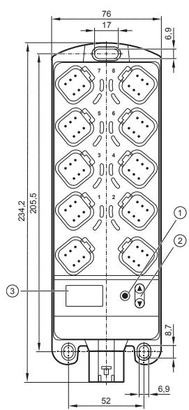


1: Taste ENTER
2: Tasten UP/DOWN
3: 10-Segment-Anzeige
4: DEUTSCH-Stecker
5: AMP-Anschlussstecker
Technische Daten
Mechanische Daten
| Gehäuse |
| Abmessungen (H x B x T) |
| Montage |
| Anschluss |
Eingänge
Ausgänge
CAN1-Schnittstelle
Betriebsspannung, CAN2
Schutzart
Betriebs-/Lagertemperatur
Max. zulässige relative Luftfeuchtigkeit
Max. Höhe über NN
Verschmutzungsgrad
Gewicht
Elektrische Daten
Betriebsspannung
| Stromaufnahme |
Überspannung
Unterspannungserkennung
Unterspannungsabschaltung
Prozessor
Speicher (gesamt)
Speicheraufteilung
Modulares Steuerungssystem
Einsetzbar als CANopen-Device oder intelligentes E/A-Modul
| Gehäuse: PA6/6.6 Anzeigefenster: PATasten: Silikon |
| 234 x 76 x 40,5 mm (ohne Rohrniete) |
| Befestigung mit 3 Schrauben M5 nach DIN EN ISO 4762 oder DIN 7984, 3 Rohrnieten nach DIN 7340 und 3 Unterlegscheiben nach DIN EN ISO 7092 (Rohrniete und Unterlegscheiben liegen bei) |
| Versorgung: MCP2.8 6 polig für Stecker TE-AMP 1745078-1 Ein-/Ausgänge: Deutsch DT04-6S 6 polig Kontakte: AMP: CuFe verzinnt; Deutsch: CuZn vergoldet |
| 4 x 6-polig4 x 6-polig2 x 6-polig1 x 6-polig |
| IP 65 und IP 67 (alle Stecker gesteckt) |
| -40...85°C / -40...85°C |
| 90 %, nicht kondensierend |
| 2000 m |
| 2 |
| 450 g |
| 8...32 V DC |
| 105 mA (bei 24 V DC) / 188 mA (bei 12 V DC) / max. 300 mA |
| 36 V für t ≤ 10 sbei UB ≤ 7,8 Vbei UB ≤ 7,0 V |
| Freescale PowerPC, 50 MHz |
| 592 kByte RAM / 1536 kByte Flash / 1 kByte FRAM |
| siehe Programmierhandbuch ioControl undwww.ifm.com |
CR2052
Geräteüberwachung
CAN Schnittstellen 1 und 2
Baudrate
Kommunikationsprofil
Software/Programmierung
Programmiersystem
Eingänge
Konfigurationen
Ausgänge
Konfigurationen
Anzeigeelemente
I/O-LEDs
Power-LED (PWR)
Mode-LED (M)
Applications-LEDs (A... D)
Lock-LED (Schloss-Symbol)
Diagnose-LED (DIA)
Anzeige
Technische Daten
Unterspannungsüberwachung
Watchdogfunktion
Checksummenprüfung für Programm und System
Übertemperaturüberwachung
CAN Interface 2.0 A/B, ISO 11898
20 kBit/s...1 MBit/s (Default CAN1: 250 kBit/s, CAN2: 250 kBit/s)
CANopen, CiA DS 301 Version 4, CiA DS 401 Version 1.4
oder SAE J 1939 oder freies Protokoll
CODESYS Version 2.3 (IEC 61131-3)
8 (konfigurierbar)
| Anzahl | Ausführung | |
| 4 | digital für positive/negative Gebersignale analog (0...10/32 V DC, 0...20 mA, ratiometrisch) Frequenz (≤ 30 kHz) | BL/BH AFRQ |
| 4 | digital für positive Gebersignale Widerstandsmessung (0,016...30 kΩ) | BL R |
8 (konfigurierbar)
| Anzahl | Ausführung | |
| 4 | plusschaltend (High-Side), 4 A, DiagnosePWM-Ausgang (20...250 Hz), 4 A, Diagnosestromgeregelt 0,02...4 A | BH PWM PWMI |
| 4 | plusschaltend (High-Side), 2,5 A, DiagnosePWM-Ausgang (20...250 Hz), 2,5 A, Diagnosestromgeregelt 0,02...2,5 A | BH PWM PWMI |
16 x LED orange
(Voreinstellung: Statusanzeige des jeweiligen Ein-/Ausgangs)
LED grün
(Voreinstellung: Signalisieren des System-Status)
LED grün
(Voreinstellung: Signalisiert eine Anzeige der Node-ID)
4 x LED grün
1 x LED grün
(Voreinstellung: Verriegelung der eingestellten Parameter)
1 x LED rot
(Voreinstellung: Anzeigen eines Fehlers)
4-stellige 10-Segment-Anzeige (zweifarbig: rot / grün)
(Voreinstellung: Anzeige der Baudrate oder Node-ID)
CR2052
Betriebszustände bei Verwendung als Mobilsteuerung
Bedienelemente
Tasten
Tasten (Voreinstellung)
Kennwerte der Eingänge
Analogeingänge ( BL , BH , A, FRQ)
IN00 - Anschluss 1, Pin 5
IN01 - Anschluss 3, Pin 5
IN04 - Anschluss 1, Pin 2
IN05 - Anschluss 3, Pin 2
konfigurierbar als...
Technische Daten
| LED | Zustand | Beschreibung |
| - | konstant aus | keine Betriebsspannung |
| PWR + DIA | 1 x ein | Initialisierung oder Reset Checks |
| PWR | 5 Hz | kein Betriebssystem geladen |
| 2 Hz | Applikation läuft (RUN) | |
| konstant ein | Applikation angehalten (STOP) | |
| DIA | 10 Hz | Applikation angehalten (STOP mit Fehler) |
| 5 Hz | Applikation angehalten wegen Unterspannung | |
| konstant ein | System-Fehler (Fatal Error) |
ENTER, UP, DOWN
Einstellen der CAN-ID / Baudrate
| Spannungseingänge | |
| Eingangsspannung | 0...10 V oder 0...32 V |
| Auflösung | 12 Bit |
| Genauigkeit | ± 1% FS |
| Eingangswiderstand | 65,6 kΩ (0...10 V), 50,7 kΩ (0...32 V) |
| Eingangsfrequenz | ≤ 500 Hz |
| Stromeingänge, diagnosefähig | |
| Eingangsstrom | 0...20 mA |
| Auflösung | 12 Bit |
| Genauigkeit | ± 1% FS |
| Eingangswiderstand | 400 Ω |
| Eingangsfrequenz | ≤ 500 Hz |
| Bei Strömen > 23 mA wird der Eingang auf Spannungseingang umgeschaltet! | |
| Spannungseingänge, 0...32 V, ratiometrisch | |
| Funktion | (UIN ÷ UB) × 1000 ‰ |
| Wertebereich | 0...1000 ‰ |
| Eingangswiderstand | 50,7 kΩ |
| Binäre Spannungseingänge für positive Gebersignale | |
| Einschaltpegel | > 0,7 UB |
| Ausschaltpegel | < 0,3 UB |
| Eingangswiderstand | 3,2 kΩ |
| Eingangsfrequenz | 50 Hz |
| Diagnose Leiterbruch | > 0,95 UB |
| Diagnose Kurzschluss | < 1 V |
| Binäre Spannungseingänge für negative Gebersignale | |
| Einschaltpegel | > 0,7 UB |
| Ausschaltpegel | < 0,3 UB |
| Eingangswiderstand | 3,2 kΩ |
| Eingangsfrequenz | 50 Hz |
| Frequenzeingänge | |
| Eingangswiderstand | 3,2 kΩ |
| Eingangsfrequenz | ≤ 30 kHz |
| Einschaltpegel | > 0,7 UB |
| Ausschaltpegel | < 0,3 UB |
CR2052
Digitaleingänge (B L , R)
IN02 - Anschluss 5, Pin 5
IN03 - Anschluss 7, Pin 5
IN06 - Anschluss 5, Pin 2
IN07 - Anschluss 7, Pin 2
konfigurierbar als...
Kennwerte der Ausgänge
Digitalausgänge (B H , PWM, PWM I )
OUT00 - Anschluss 2, Pin 5
OUT01 - Anschluss 4, Pin 5
OUT02 - Anschluss 6, Pin 5
OUT03 - Anschluss 8, Pin 5
konfigurierbar als...
Technische Daten
| ● Binäre Spannungseingänge für positive Gebersignale | |
| Einschaltpegel | >0,7 UB |
| Ausschaltpegel | <0,3 UB |
| Eingangswiderstand | 3,2 kΩ |
| Eingangsfrequenz | 50 Hz |
| Diagnose Leiterbruch | >0,95 UB |
| Diagnose Kurzschluss | <1 V |
| ● Widerstandseingang | |
| Messbereich | 0,016...30 kΩ |
| Genauigkeit | ± 2 % FS: 16 Ω...3 kΩ ± 5 % FS: 3...15 kΩ ± 10 % FS: 15...30 kΩ |
| Halbleiterausgänge, plusschaltend (High-Side), kurzschluss- und überlastfest. Diagnose über Stromrücklesung (Leiterbruch / Überlast)Diagnose über Spannungsrücklesung, Pullup-Widerstand abschaltbar (Leiterbruch/Kurzschluss) | |
| Schaltspannung | 8...32 V |
| Schaltstrom | 0,02...4 A |
| Lastwiderstand | ≥ 3 Ω (bei 12 V DC) ≥ 6 Ω (bei 24 V DC) |
| Strommessbereich | 0,02...6 A |
| Genauigkeit Stromrücklesung | 1 % FS |
| PWM-Ausgänge | |
| Ausgangsfrequenz | 20...250 Hz |
| Tastverhältnis | 1...1000 ‰ |
| Schaltstrom | 0,02...4 A |
| Strommessbereich | 0,02...6 A |
| Genauigkeit Stromrücklesung | 3 % FS |
| Stromgeregelter Ausgang | |
| Ausgangsfrequenz | 20...250 Hz |
| Regelbereich | 0,02...4 A |
| Einstellauflösung | 1 mA |
| Max. Einschaltstrom | ≤ 24 A |
| Genauigkeit Stromrücklesung | 3 % FS |
CR2052
Digitalausgänge (B H , PWM, PWM I )
OUT04 - Anschluss 2, Pin 2
OUT05 - Anschluss 4, Pin 2
OUT06 - Anschluss 6, Pin 2
OUT07 - Anschluss 8, Pin 2
konfigurierbar als...
Freilaufdioden
Überlastfestigkeit
(Gültig für alle Ausgänge)
Kurzschlussfestigkeit
(gültig für alle Ein- und Ausgänge)
Max. Summenstrom der CAN-
Versorgung + Sensorversorgungen VCAN + VBBS
Max. Summenstrom der
Ausgangsversorgungen VBB 2
(Dauerstrombelastung)
Technische Daten
| Halbleiterausgänge, plusschaltend (High-Side), kurzschluss- und überlastfest. Diagnose über Stromrücklesung (Leiterbruch / Überlast)Diagnose über Spannungsrücklesung, Pullup-Widerstand abschaltbar (Leiterbruch/Kurzschluss) | |
| Schaltspannung | 8...32 V |
| Schaltstrom | 0,02...2,5 A |
| Lastwiderstand | ≥ 4,8 Ω (bei 12 V DC) ≥ 9,6 Ω (bei 24 V DC) |
| Strommessbereich | 0,02...4 A |
| Genauigkeit Stromrücklesung | 1 % FS |
| PWM-Ausgänge | |
| Ausgangsfrequenz | 20...250 Hz |
| Tastverhältnis | 1...1000 ‰ |
| Schaltstrom | 0,02...2,5 A |
| Strommessbereich | 0,02...4 A |
| Genauigkeit Stromrücklesung | 3 % FS |
| Stromgeregelter Ausgang | |
| Ausgangsfrequenz | 20...250 Hz |
| Regelbereich | 0,02...2,5 A |
| Einstellauflösung | 1 mA |
| Max. Einschaltstrom | ≤ 24 A |
| Genauigkeit Stromrücklesung | 3 % FS |
Freilaufdioden zur Abschaltung induktiver Lasten sind integriert
≤ 5 Minuten (bei 100% Überlast)
≤ 5 Minuten
1,5 A

1: Montage Fahrzeug im Außenbereich (externe Konvektion)
2: Montage im Schaltschrank auf Metallplatte oder Montage auf schlecht wärmeleitfähigem Untergrund (z. B. Kuststoff oder Holz)
| CR2052 | Technische Daten | |
| Prüfnormen und Bestimmungen | ||
| CE-Zeichen | EN 61000-6-2 | Elektromagnetische Verträglichkeit (EMV)Störfestigkeit |
| EN 61000-6-4 | Elektromagnetische Verträglichkeit (EMV)Störaussendung | |
| E1-Zeichen | UN/ECE-R10 | Störaussendung Störfestigkeit mit 100 V/m |
| ISO 7637-2 | Impuls 1, Schärfegrad: IV; Funktionszustand CImpuls 2a, Schärfegrad: IV; Funktionszustand AImpuls 2b, Schärfegrad: IV; Funktionszustand CImpuls 3a, Schärfegrad: IV; Funktionszustand AImpuls 3b, Schärfegrad: IV; Funktionszustand AImpuls 4, Schärfegrad: IV; Funktionszustand BImpuls 5, Schärfegrad: III; Funktionszustand C(Angaben gelten für 24 V System)Impuls 4, Schärfegrad: III; Funktionszustand C(Angabe gilt für 12 V System) | |
| Klimatische Prüfungen | EN 60068-2-30 | Feuchte Wärme zyklischobere Temperatur 55°C, Anzahl Zyklen: 6 |
| EN 60068-2-78 | Feuchte Wärme konstant Prüftemperatur 40°C / 93% RH,Prüfdauer: 21 Tage | |
| Mechanische Prüfungen | ISO 16750-3 | Test VII; Vibration, random Anbauort Karosserie |
| EN 60068-2-6 | Vibration, Sinus10...500 Hz; 0,72 mm/10 g; 10 Zyklen/Achse | |
| ISO 16750-3 | Dauerschocken30 g/6 ms; 24.000 Schocks | |
| Chemische Beständigkeit | ISO 16750-5:2010 | AA, BA, BD, CC, DB, DC, DDimmer nur eine Chemikalie gleichzeitig zulässig |
| Hinweis | EG-Konformitätserklärung und Zulassungen sind abrufbar unter:www.ifm.com | |
ifm electronic gmbh • Friedrichstraße 1 • 45128 Essen
Technische Änderungen behalten wir uns ohne Ankündigung vor!
CR2052 / Seite 6 02.09.2024
CR2052
Anschlussbelegung
Technische Daten
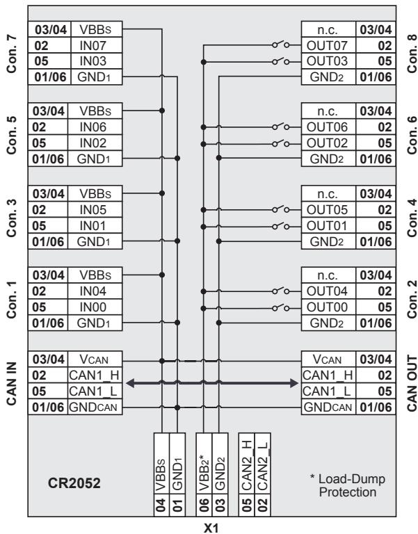
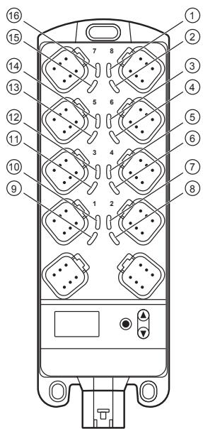
LED-Zuordnung
| Deutsch-Stecker | AMP-Stecker |
 | 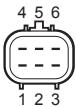 |
1: LED OUT07
2: LED OUT03
3: LED OUT06
4: LED OUT02
5: LED OUT05
6: LED OUT01
7: LED OUT04
8: LED OUT00
9: LED IN04
10: LED IN00
11: LED IN05
12: LED IN01
13: LED IN06
14: LED IN02
15: LED IN07
16: LED IN03
| CR2052 | Technische Daten |
| Abkürzungen | A AnalogR WiderstandseingangFRQ Frequenz-/ImpulseingangBH Binär High-SideBL Binär Low-SidePWM PulsweitenmodulationPWM1 Pulsweitenmodulation, stromgeregeltVBB5 Versorgung Sensorik/ModulVBB2 Versorgung OUT01... OUT07VCAN Versorgung CAN-Stecker |
ifm electronic gmbh • Friedrichstraße 1 • 45128 Essen
Technische Änderungen behalten wir uns ohne Ankündigung vor!
CR2052 / Seite 8 02.09.2024
10 Wartung, Instandsetzung und Entsorgung
Das Gerät ist wartungsfrei.
▶ Da innerhalb des Gerätes keine vom Anwender zu wartenden Bauteile enthalten sind, das Gehäuse nicht öffnen. Die Instandsetzung des Gerätes darf nur durch den Hersteller erfolgen.

Bei Gerätetausch Verschmutzungsgrad einhalten ( → 9 Technische Daten), bis Schutzart durch Stecker / Blindstopfen sichergestellt ist. Gerät / Stecker vor Tausch reinigen, falls erforderlich. Dichtungen der Stecker auf Wiederverwendbarkeit prüfen. Schutzart ist nur bei intakten Dichtungen gewährleistet.
▶ Reinigung des Geräts mit einem trockenen Tuch.

Folgende Mittel sind zur Gerätereinigung ungeeignet: Kunststofflösende Chemikalien, wie z. B. Isopropanol, Brennspiritus, Benzin, Verdünner, Alkohol, Azeton oder Ammoniak.
▶ Das Gerät gemäß den nationalen Umweltvorschriften entsorgen.
11 Zulassungen/Normen
Prüfnormen und Bestimmungen ( → 9 Technische Daten)
Die EU-Konformitätserklärung und Zulassungen sind abrufbar unter: www.ifm.com
12 Appendix
12.1 EMCY Object
The following error codes according to DSP-401 or DSP-301 are supported:
| EMCY code | Error reg | Additional code | Description |
| 0x6100 | 0x11 | 0x00 | "Internal Software Overflow of an Rx queue e.g. frequency of the RxP-DOs is too high. Reset only externally via entry in the index 0x1003 Subldx 00." |
| 0x6101 | 0x11 | 0x00 | "Internal Software Overflow of an Tx queue e.g. device does not communicate with the bus. Reset only externally via entry in the index 0x1003 Subldx 00." |
| 0x8000 | 0x11 | 0x00 | "Monitoring Sync Error For communication cycle no sync object is received. Only in Operational. Reset with the next sync OBJ or PREOP" |
| 0x8100 | 0x11 | 0x00 | Communication Err |
| 0x8131 | 0x11 | 0x00 | "Monitoring Heart Beat ErrorNo guard object is received. Reset with the next Heart beat or PREOP" |
| 0x63xx | 0x01 | 0x00 | "Invalid parameter of an input or output.""xx"" means number of the IO-channel (00 ... 15)" |
| 0x5000 | 0x01 | 0x00 | Memory Error |
| 0x3308 | 0x05 | 0x00 | VBB2 error (only CR2051, CR2052) |
| 0x90xx | 0x01 | 0x00 | "Frequency input, Frequency too low""xx"" means number of the IO-channel (00 ... 15)" |
| 0x21xx | 0x03 | 0x00 | "Inputs, Openline""xx"" means number of the IO-channel (00 ... 15)" |
| 0x21xx | 0x03 | 0x00 | "Inputs, Short circuit""xx"" means number of the IO-channelCR2050 (00 ... 15) + 16; CR2052 (00 ... 07) + 8" |
| 0x21xx | 0x03 | 0x00 | "Inputs, Overcurrent""xx"" means number of the IO-channelCR2050 (00 ... 15) + 32; CR2052 (00 ... 07) + 16" |
| 0x23xx | 0x03 | 0x00 | "outputs, Openline""xx"" means number of the IO-channelCR2051 (00 ... 15); CR2052 (00 ... 07)" |
| 0x23xx | 0x03 | 0x00 | "outputs, Short circuit""xx"" means number of the IO-channelCR2051 (00 ... 15) + 16; CR2052 (00 ... 07) + 8" |
| 0x23xx | 0x03 | 0x00 | "outputs, Overload""xx"" means number of the IO-channelCR2051 (00 ... 15) + 32; CR2052 (00 ... 07) + 16" |
CANopen does not provide for two identical EMCY objects to be sent consecutively.
12.2 Object directory CR205x
Obligatory objects (index 0x1000...0x1FFF):
| Index | S-idx | Designation | Data type | Default | Details (CR205x) | |
| 0x1000 | Device type | ro | UDINT | 0x000F0191 | Device type | |
| 0x1001 | Error register | ro | USINT | 0 | Error register bitcoded to profile 301 Permissible values:0b0000 0000 = no error0b0000 0001 = generic error0b0001 0000 = communication error0b1000 0000 = manufacturer specific | |
| 0x1018 | 0x00 | Device identification Number of entries | ro | USINT | 0x04 | Device identification |
| 0x01 | Vendor-ID | ro | UDINT | 0x0069666D | Vendor ID of the device according to CiA specification | |
| 0x02 | Product code | ro | STRING | 0 | Product code of the device | |
| 0x03 | Revision number | ro | UDINT | 0 | Revision number of the device | |
| 0x04 | Serial number | ro | UDINT | 0 | Serial number of the device | |
| 0x1003 | 0x00 | Predefined error field Number of entries | rw | UDINT | 0 | An error list with 4 entries is supported |
| 0x01 | Error history | ro | UDINT | 0 | Error occurred, coded according to EMCY list The last error is indicated in the sub-index 1 | |
| 0x02 | Error history | ro | UDINT | 0 | Error occurred, coded according to EMCY list | |
| 0x03 | Error history | ro | UDINT | 0 | Error occurred, coded according to EMCY list | |
| 0x04 | Error history | ro | UDINT | 0 | Error occurred, coded according to EMCY list | |
| 0x05 | Error history | ro | UDINT | 0 | Error occurred, coded according to EMCY list | |
| 0x1005 | COB-ID synch message | rw | UDINT | 0x0000 0080 | Identifier of the synch message Bit 30 = 0 → device generates no synch message Bit 30 = 1 → device generates a synch message Bit 29 = 0 → 11 bit IDBit 29 = 1 → ID = 0x80 + node ID | |
| 0x1006 | Communi-cation cycle period | rw | UDINT | 0 | Max. time between 2 synch objects in [μs] Control resolution = 1 ms | |
| 0x1008 | Manufacturer device name | ro | STRING | CR205x | Device designation (CR2050 or CR2051 or CR2052) | |
| 0x1009 | Manufacturer hardware version | ro | STRING | V00.00.00 | Hardware version | |
| 0x100A | Manufacturer software version | ro | STRING | V00.00.00 | Software version | |
| 0x1010 | 0x00 | Store para-meters Largest sub-index supported | ro | USINT | 0x01 | Number of "save options" |
| 0x01 | Save all parameters | rw | UDINT | 2 | Automatic saving of all parameters changed0 = AutoSave OFF2 = AutoSave ON | |
| 0x1011 | 0x00 | Restore default parameters Largest sub-index supported | ro | USINT | 0x01 | Number of "restore options" |
| 0x01 | Restore all default parameters | rw | UDINT | 0x01 | If the String "load" is entered here, the default parameters set at the factory are restored and become valid after the next reset. | |
| 0x1014 | COBId Emergency | rw | UDINT | 0x80 + node ID | Bit 31 = 0 → EMCY is valid Bit 31 = 1 → EMCY is not valid Bit 29 = 0 → 11-bit IDBit 29 = 1 → ID = 0x80 + node IDCAN identifier can be changed by the user. | |
| 0x1016 | 0x00 | Consumer heartbeat times Nums consumer heartbeat time | ro | USINT | 0x01 | Heartbeat monitoring time for the node Number of devices monitored = 1 |
| 0x01 | Consumer heartbeat time | rw | UDINT | 0 | Heartbeat monitoring time for the node Format: 0x0nntttttttt = monitoring time [ms]nn = node numberif nn=0 or tttt=0 → no monitoring | |
| 0x1017 | Producer heartbeat time | rw | UINT | 0 | Time intervall [ms] during which the device generates a producer heartbeat | |
12.2.1 Device-specific CR2050
Transmit PDO communication parameters (index 0x1800...0x18FF):
| Index | S-idx | Designation | Data type | Default | Details (CR2050) | |
| 0x1800 | 0x00 | Transmit PDO Communication Parameter Number of entries | ro | USINT | 0x05 | Configuration transmit PDO 1 number of entries = 5 |
| 0x01 | COBID used by PDO | rw | UDINT | 0x180 + Node ID | CAN ID of the transmit PDO 1 Bit 31 = 0 → PDO is valid Bit 31 = 1 → PDO is not valid | |
| 0x02 | transmission type | rw | USINT | 0xFF | 0x00 = synch acyclic 0x01...0xF0 = synch cyclic; values are only transmitted after „n" synch objects n = 1...240 = 0x01...0xF0 0xFC/0xFD not implemented 0xFE = asynch man. spec. event; values are immediately transferred 0xFF = asynch device profile event; values are immediately transferred | |
| 0x03 | inhibit time | rw | UINT | 0 | delay time in the transmission type "asynch" before the PDO is transmitted again at the earliest. (0...65535 • 100 μs) | |
| 0x04 | reserved | rw | USINT | 0 | reserve | |
| 0x05 | event time | rw | UINT | 0 | max. transfer break in the transmission type „asynch" (0...65535 ms) When this time has elapsed, the PDO is transferred even if the appl. event has not accrued. | |
| 0x1801 | 0x00 | Transmit PDO Communication Parameter Number of entries | ro | USINT | 0x05 | Configuration transmit PDO 2 number of entries = 5 |
| 0x01 | COBID used by PDO | rw | UDINT | 0x280 + Node ID | CAN ID of the transmit PDO 2 Bit 31 = 0 → PDO is valid Bit 31 = 1 → PDO is not valid | |
| 0x02 | transmission type | rw | USINT | 0x01 | 0x00 = synch acyclic 0x01...0xF0 = synch cyclic; values are only transmitted after „n" synch objects n = 1...240 = 0x01...0xF0 0xFC/0xFD not implemented 0xFE = asynch man. spec. event; values are immediately transferred 0xFF = asynch device profile event; values are immediately transferred | |
| 0x03 | inhibit time | rw | UINT | 0 | delay time in the transmission type "asynch" before the PDO is transmitted again at the earliest. (0...65535 • 100 μs) | |
| 0x04 | reserved | rw | USINT | 0 | reserve | |
| 0x05 | event time | rw | UINT | 0 | max. transfer break in the transmission type „asynch" (0...65535 ms) When this time has elapsed, the PDO is transferred even if the appl. event has not accrued. | |
| 0x1802 | 0x00 | Transmit PDO Communication Parameter Number of entries | ro | USINT | 0x05 | Configuration transmit PDO 3 number of entries = 5 |
| 0x01 | COBID used by PDO | rw | UDINT | 0x380 + Node ID | CAN ID of the transmit PDO 3 Bit 31 = 0 → PDO is valid Bit 31 = 1 → PDO is not valid | |
| 0x02 | transmission type | rw | USINT | 0x01 | 0x00 = synch acyclic 0x01...0xF0 = synch cyclic; values are only transmitted after „n" synch objects n = 1...240 = 0x01...0xF0 0xFC/0xFD not implemented 0xFE = asynch man. spec. event; values are immediately transferred 0xFF = asynch device profile event; values are immediately transferred | |
| 0x03 | inhibit time | rw | UINT | 0 | delay time in the transmission type "asynch" before the PDO is transmitted again at the earliest. (0...65535 • 100 μs) | |
| 0x04 | reserved | rw | USINT | 0 | reserve | |
| 0x05 | event time | rw | UINT | 0 | max. transfer break in the transmission type „asynch" (0...65535 ms) When this time has elapsed, the PDO is transferred even if the appl. event has not accrued. | |
| 0x1803 | 0x00 | Transmit PDO Communication Parameter Number of entries | ro | USINT | 0x05 | Configuration transmit PDO 4 number of entries = 5 |
| 0x01 | COBID used by PDO | rw | UDINT | 0x480 + Node ID | CAN ID of the transmit PDO 4 Bit 31 = 0 → PDO is valid Bit 31 = 1 → PDO is not valid | |
| 0x02 | transmission type | rw | USINT | 0x01 | 0x00 = synch acyclic 0x01...0xF0 = synch cyclic; values are only transmitted after „n" synch objects n = 1...240 = 0x01...0xF0 0xFC/0xFD not implemented 0xFE = asynch man. spec. event; values are immediately transferred 0xFF = asynch device profile event; values are immediately transferred | |
| 0x03 | inhibit time | rw | UINT | 0 | delay time in the transmission type "asynch" before the PDO is transmitted again at the earliest. (0...65535 • 100 μs) | |
| 0x04 | reserved | rw | USINT | 0 | reserve | |
| 0x05 | event time | rw | UINT | 0 | max. transfer break in the transmission type „asynch" (0...65535 ms) When this time has elapsed, the PDO is transferred even if the appl. event has not accrued. | |
| 0x1804 | 0x00 | Transmit PDO Communication Parameter Number of entries | ro | USINT | 0x05 | Configuration transmit PDO 5 number of entries = 5 |
| 0x01 | COBID used by PDO | rw | UDINT | 0x181 + Node ID | CAN ID of the transmit PDO 5 Bit 31 = 0 → PDO is valid Bit 31 = 1 → PDO is not valid | |
| 0x02 | transmission type | rw | USINT | 0x01 | 0x00 = synch acyclic 0x01...0xF0 = synch cyclic; values are only transmitted after „n" synch objects n = 1...240 = 0x01...0xF0 0xFC/0xFD not implemented 0xFE = asynch man. spec. event; values are immediately transferred 0xFF = asynch device profile event; values are immediately transferred | |
| 0x03 | inhibit time | rw | UINT | 0 | delay time in the transmission type "asynch" before the PDO is transmitted again at the earliest. (0...65535 • 100 μs) | |
| 0x04 | reserved | rw | USINT | 0 | reserve | |
| 0x05 | event time | rw | UINT | 0 | max. transfer break in the transmission type „asynch" (0...65535 ms) When this time has elapsed, the PDO is transferred even if the appl. event has not accrued. | |
| 0x1805 | 0x00 | Transmit PDO Communication Parameter Number of entries | ro | USINT | 0x05 | Configuration transmit PDO 6 number of entries = 5 |
| 0x01 | COBID used by PDO | rw | UDINT | 0x281 + Node ID | CAN ID of the transmit PDO 6 Bit 31 = 0 → PDO is valid Bit 31 = 1 → PDO is not valid | |
| 0x02 | transmission type | rw | USINT | 0x01 | 0x00 = synch acyclic 0x01...0xF0 = synch cyclic; values are only transmitted after „n" synch objects n = 1...240 = 0x01...0xF0 0xFC/0xFD not implemented 0xFE = asynch man. spec. event; values are immediately transferred 0xFF = asynch device profile event; values are immediately transferred | |
| 0x03 | inhibit time | rw | UINT | 0 | delay time in the transmission type "asynch" before the PDO is transmitted again at the earliest. (0...65535 • 100 μs) | |
| 0x04 | reserved | rw | USINT | 0 | reserve | |
| 0x05 | event time | rw | UINT | 0 | max. transfer break in the transmission type „asynch" (0...65535 ms) When this time has elapsed, the PDO is transferred even if the appl. event has not accrued. | |
| 0x1806 | 0x00 | Transmit PDO Communication Parameter Number of entries | ro | USINT | 0x05 | Configuration transmit PDO 7 number of entries = 5 |
| 0x01 | COBID used by PDO | rw | UDINT | 0x381 + Node ID | CAN ID of the transmit PDO 7 Bit 31 = 0 → PDO is valid Bit 31 = 1 → PDO is not valid | |
| 0x02 | transmission type | rw | USINT | 0x01 | 0x00 = synch acyclic 0x01...0xF0 = synch cyclic; values are only transmitted after „n" synch objects n = 1...240 = 0x01...0xF0 0xFC/0xFD not implemented 0xFE = asynch man. spec. event; values are immediately transferred 0xFF = asynch device profile event; values are immediately transferred | |
| 0x03 | inhibit time | rw | UINT | 0 | delay time in the transmission type "asynch" before the PDO is transmitted again at the earliest. (0...65535 • 100 μs) | |
| 0x04 | reserved | rw | USINT | 0 | reserve | |
| 0x05 | event time | rw | UINT | 0 | max. transfer break in the transmission type „asynch" (0...65535 ms) When this time has elapsed, the PDO is transferred even if the appl. event has not accrued. | |
| 0x1807 | 0x00 | Transmit PDO Communication Parameter Number of entries | ro | USINT | 0x05 | Configuration transmit PDO 8 number of entries = 5 |
| 0x01 | COBID used by PDO | rw | UDINT | 0x481 + Node ID | CAN ID of the transmit PDO 8 Bit 31 = 0 → PDO is valid Bit 31 = 1 → PDO is not valid | |
| 0x02 | transmission type | rw | USINT | 0x01 | 0x00 = synch acyclic 0x01...0xF0 = synch cyclic; values are only transmitted after „n" synch objects n = 1...240 = 0x01...0xF0 0xFC/0xFD not implemented 0xFE = asynch man. spec. event; values are immediately transferred 0xFF = asynch device profile event; values are immediately transferred | |
| 0x03 | inhibit time | rw | UINT | 0 | delay time in the transmission type "asynch" before the PDO is transmitted again at the earliest. (0...65535 • 100 μs) | |
| 0x04 | reserved | rw | USINT | 0 | reserve | |
| 0x05 | event time | rw | UINT | 0 | max. transfer break in the transmission type „asynch" (0...65535 ms) When this time has elapsed, the PDO is transferred even if the appl. event has not accrued. | |
| 0x1808 | 0x00 | Transmit PDO Communication Parameter Number of entries | ro | USINT | 0x05 | Configuration transmit PDO 9 number of entries = 5 |
| 0x01 | COBID used by PDO | rw | UDINT | 0x182 + Node ID | CAN ID of the transmit PDO 9 Bit 31 = 0 → PDO is valid Bit 31 = 1 → PDO is not valid | |
| 0x02 | transmission type | rw | USINT | 0x01 | 0x00 = synch acyclic 0x01...0xF0 = synch cyclic; values are only transmitted after „n" synch objects n = 1...240 = 0x01...0xF0 0xFC/0xFD not implemented 0xFE = asynch man. spec. event; values are immediately transferred 0xFF = asynch device profile event; values are immediately transferred | |
| 0x03 | inhibit time | rw | UINT | 0 | delay time in the transmission type "asynch" before the PDO is transmitted again at the earliest. (0...65535 • 100 μs) | |
| 0x04 | reserved | rw | USINT | 0 | reserve | |
| 0x05 | event time | rw | UINT | 0 | max. transfer break in the transmission type „asynch" (0...65535 ms) When this time has elapsed, the PDO is transferred even if the appl. event has not accrued. | |
| 0x1809 | 0x00 | Transmit PDO Communication Parameter Number of entries | ro | USINT | 0x05 | Configuration transmit PDO 10 number of entries = 5 |
| 0x01 | COBID used by PDO | rw | UDINT | 0x282 + Node ID | CAN ID of the transmit PDO 10 Bit 31 = 0 → PDO is valid Bit 31 = 1 → PDO is not valid | |
| 0x02 | transmission type | rw | USINT | 0x01 | 0x00 = synch acyclic 0x01...0xF0 = synch cyclic; values are only transmitted after „n" synch objects n = 1...240 = 0x01...0xF0 0xFC/0xFD not implemented 0xFE = asynch man. spec. event; values are immediately transferred 0xFF = asynch device profile event; values are immediately transferred | |
| 0x03 | inhibit time | rw | UINT | 0 | delay time in the transmission type "asynch" before the PDO is transmitted again at the earliest. (0...65535 • 100 μs) | |
| 0x04 | reserved | rw | USINT | 0 | reserve | |
| 0x05 | event time | rw | UINT | 0 | max. transfer break in the transmission type „asynch" (0...65535 ms) When this time has elapsed, the PDO is transferred even if the appl. event has not accrued. | |
Transmit PDO mapping (index 0x1A00...0x1AFF):
| Index | S-idx | Designation | Data type | Default | Details (CR2050) | |
| 0x1A00 | 0x00 | Transmit PDO mapping Number of mapped objects in PDO | rw | USINT | 0x07 | mapping transmit PDO 1 number of integrated application objects = 7 |
| 0x01 | PDO mapping | rw | UDINT | 0x6000 0108 | Index 0x6000, SubIndex 0x01 binary inputs 00...07: actual values (bit coded) | |
| 0x02 | PDO mapping | rw | UDINT | 0x6000 0208 | Index 0x6000, SubIndex 0x02 binary inputs 08...15: actual values (bit coded) | |
| 0x03 | PDO mapping | rw | UDINT | 0x2020 0108 | Index 0x2020, SubIndex 0x01 binary inputs 00...07: flag "short circuit" (bit coded) | |
| 0x04 | PDO mapping | rw | UDINT | 0x2020 0208 | Index 0x2020, SubIndex 0x02 binary inputs 08...15: flag "short circuit" (bit coded) | |
| 0x05 | PDO mapping | rw | UDINT | 0x2021 0108 | Index 0x2021, SubIndex 0x01 outputs 00...07: flag " wire break " (bit coded) | |
| 0x06 | PDO mapping | rw | UDINT | 0x2021 0208 | Index 0x2021, SubIndex 0x02 outputs 08...15: flag " wire break " (bit coded) | |
| 0x07 | PDO mapping | rw | UDINT | 0x2025 0108 | Index 0x2025, SubIndex 0x01 inputs 00...03: flag " overload " (bit coded) | |
| 0x1A01 | 0x00 | Transmit PDO mapping Number of mapped objects in PDO | rw | USINT | 0x04 | mapping transmit PDO 2 (analogue inputs)number of integrated application objects = 4 |
| 0x01 | PDO mapping | rw | UDINT | 0x6404 0110 | Index 0x6404, SubIndex 0x01 analogue input 00: actual value (depending on the configuration 0x2000) | |
| 0x02 | PDO mapping | rw | UDINT | 0x6404 0210 | Index 0x6404, SubIndex 0x02 analogue input 01: actual value (depending on the configuration 0x2000)) | |
| 0x03 | PDO mapping | rw | UDINT | 0x6404 0310 | Index 0x6404, SubIndex 0x03 analogue input 02: actual value (depending on the configuration 0x2000) | |
| 0x04 | PDO mapping | rw | UDINT | 0x6404 0410 | Index 0x6404, SubIndex 0x04 analogue input 03: actual value (depending on the configuration 0x2000) | |
| 0x1A02 | 0x00 | Transmit PDO mapping Number of mapped objects in PDO | rw | USINT | 0x04 | mapping transmit PDO 3 (analogue inputs)number of integrated application objects = 4 |
| 0x01 | PDO mapping | rw | UDINT | 0x6404 0510 | Index 0x6404, SubIndex 0x05 analogue input 04: actual value (depending on the configuration 0x2000) | |
| 0x02 | PDO mapping | rw | UDINT | 0x6404 0610 | Index 0x6404, SubIndex 0x06 analogue input 05: actual value (depending on the configuration 0x2000)) | |
| 0x03 | PDO mapping | rw | UDINT | 0x6404 0710 | Index 0x6404, SubIndex 0x07 analogue input 06: actual value (depending on the configuration 0x2000) | |
| 0x04 | PDO mapping | rw | UDINT | 0x6404 0810 | Index 0x6404, SubIndex 0x08 analogue input 07: actual value (depending on the configuration 0x2000) | |
| 0x1A03 | 0x00 | Transmit PDO mapping Number of mapped objects in PDO | rw | USINT | 0x04 | mapping transmit PDO 4 number of integrated application objects = 4 |
| 0x01 | PDO mapping | rw | UDINT | 0x2030 0110 | Index 0x2030, SubIndex 0x01 input 08: actual resistor value | |
| 0x02 | PDO mapping | rw | UDINT | 0x2030 0210 | Index 0x2030, SubIndex 0x02 input 10: actual resistor value | |
| 0x03 | PDO mapping | rw | UDINT | 0x2030 0310 | Index 0x2030, SubIndex 0x03 input 12: actual resistor value | |
| 0x04 | PDO mapping | rw | UDINT | 0x2030 0410 | Index 0x2030, SubIndex 0x04 input 14: actual resistor value | |
| 0x1A04 | 0x00 | Transmit PDO mapping Number of mapped objects in PDO | rw | USINT | 0x02 | mapping transmit PDO 5 (periode time IN09, IN11) number of integrated application objects = 2 |
| 0x01 | PDO mapping | rw | UDINT | 0x2012 0120 | Index 0x2012, SubIndex 0x01 frequency input IN09: periode time of the signal | |
| 0x02 | PDO mapping | rw | UDINT | 0x2012 0220 | Index 0x2012, SubIndex 0x02 frequency input IN11: periode time of the signal | |
| 0x1A05 | 0x00 | Transmit PDO mapping Number of mapped objects in PDO | rw | USINT | 0x02 | mapping transmit PDO 6 (periode time IN13, IN15) number of integrated application objects = 2 |
| 0x01 | PDO mapping | rw | UDINT | 0x2012 0320 | Index 0x2012, SubIndex 0x03 frequency input IN13: periode time of the signal | |
| 0x02 | PDO mapping | rw | UDINT | 0x2012 0420 | Index 0x2012, SubIndex 0x04 frequency input IN15: periode time of the signal | |
| 0x1A06 | 0x00 | Transmit PDO mapping Number of mapped objects in PDO | rw | USINT | 0x04 | mapping transmit PDO 7 (duty cycle of the signal on the frequency input IN09, IN11, IN13, IN15) number of integrated application objects = 4 |
| 0x01 | PDO mapping | rw | UDINT | 0x2014 0110 | Index 0x2014, SubIndex 0x01 frequency input IN09: duty cycle of the signal in ‰ | |
| 0x02 | PDO mapping | rw | UDINT | 0x2014 0210 | Index 0x2014, SubIndex 0x02 frequency input IN11: duty cycle of the signal in ‰ | |
| 0x03 | PDO mapping | rw | UDINT | 0x2014 0310 | Index 0x2014, SubIndex 0x03 frequency input IN13: duty cycle of the signal in ‰ | |
| 0x04 | PDO mapping | rw | UDINT | 0x2014 0410 | Index 0x2014, SubIndex 0x04 frequency input IN15: duty cycle of the signal in ‰ | |
| 0x1A07 | 0x00 | Transmit PDO mapping Number of mapped objects in PDO | rw | USINT | 0x02 | mapping transmit PDO 8 (frequency on IN09, IN11) number of integrated application objects = 2 |
| 0x01 | PDO mapping | rw | UDINT | 0x2015 0120 | Index 0x2015, SubIndex 0x01 frequency input IN09: frequency value of the signal in Hz | |
| 0x02 | PDO mapping | rw | UDINT | 0x2015 0220 | Index 0x2015, SubIndex 0x02 frequency input IN11: frequency value of the signal in Hz | |
| 0x1A08 | 0x00 | Transmit PDO mapping Number of mapped objects in PDO | rw | USINT | 0x02 | mapping transmit PDO 9 (frequency on IN13, IN15) number of integrated application objects = 2 |
| 0x01 | PDO mapping | rw | UDINT | 0x2015 0320 | Index 0x2015, SubIndex 0x03 frequency input IN13: frequency value of the signal in Hz | |
| 0x02 | PDO mapping | rw | UDINT | 0x2015 0420 | Index 0x2015, SubIndex 0x04 frequency input IN15: frequency value of the signal in Hz | |
| 0x1A09 | 0x00 | Transmit PDO mapping Number of mapped objects in PDO | rw | USINT | 0x02 | mapping transmit PDO 10 (system flag) number of integrated application objects = 2 |
| 0x01 | PDO mapping | rw | UDINT | 0x2040 0110 | Index 0x2040, SubIndex 0x01 supply voltage of the system VBBS | |
| 0x02 | PDO mapping | rw | UDINT | 0x2050 0010 | Index 0x2050, SubIndex 0x00 system temperature in °C | |
Manufacturer-specific objekts (index 0x2000...0x6FFF):
| Index | S-idx | Designation | Data type | Default | Details (CR2050) | ||
| 0x2000 | 0x00 | IO configuration Largest sub-index supported | ro | USINT | 16 | Configuration inputs/outputs largest supported Sub-index = 32 | |
| 0x01 | Configuration IN00 | rw | USINT | 10 | 0 = 0x003 = 0x036 = 0x067 = 0x079 = 0x0910 = 0x0A11 = 0x0B12 = 0x0C | off Input IN000...10 000 mV ratiometric 0...1000 %o0...20 000 μA0...32 000 mV binary plus switched binary plus switched with diagnosis binary minus switched | |
| 0x02 | Configuration IN01 | rw | USINT | 10 | 0 = 0x003 = 0x036 = 0x067 = 0x079 = 0x0910 = 0x0A11 = 0x0B12 = 0x0C | off Input IN010...10 000 mV ratiometric 0...1000 %o0...20 000 μA0...32 000 mV binary plus switched binary plus switched with diagnosis binary minus switched | |
| 0x03 | Configuration IN02 | rw | USINT | 10 | 0 = 0x003 = 0x036 = 0x067 = 0x079 = 0x0910 = 0x0A11 = 0x0B12 = 0x0C | off Input IN020...10 000 mV ratiometric 0...1000 %o0...20 000 μA0...32 000 mV binary plus switched binary plus switched with diagnosis binary minus switched | |
| 0x2000 | 0x04 | Configuration IN03 | rw | USINT | 10 | 0 = 0x003 = 0x036 = 0x067 = 0x079 = 0x0910 = 0x0A11 = 0x0B12 = 0x0C | off Input IN030...10 000 mV ratiometric 0...1000 %o0...20 000 μA0...32 000 mV binary plus switched binary plus switched with diagnosis binary minus switched |
| 0x05 | Configuration IN04 | rw | USINT | 10 | 0 = 0x003 = 0x036 = 0x067 = 0x079 = 0x0910 = 0x0A11 = 0x0B12 = 0x0C | off Input IN040...10 000 mV ratiometric 0...1000 %o0...20 000 μA0...32 000 mV binary plus switched binary plus switched with diagnosis binary minus switched | |
| 0x06 | Configuration IN05 | rw | USINT | 10 | 0 = 0x003 = 0x036 = 0x067 = 0x079 = 0x0910 = 0x0A11 = 0x0B12 = 0x0C | off Input IN050...10 000 mV ratiometric 0...1000 %o0...20 000 μA0...32 000 mV binary plus switched binary plus switched with diagnosis binary minus switched | |
| 0x07 | Configuration IN06 | rw | USINT | 10 | 0 = 0x003 = 0x036 = 0x067 = 0x079 = 0x0910 = 0x0A11 = 0x0B12 = 0x0C | off Input IN060...10 000 mV ratiometric 0...1000 %o0...20 000 μA0...32 000 mV binary plus switched binary plus switched with diagnosis binary minus switched | |
| 0x08 | Configuration IN07 | rw | USINT | 10 | 0 = 0x003 = 0x036 = 0x067 = 0x079 = 0x0910 = 0x0A11 = 0x0B12 = 0x0C | off Input IN070...10 000 mV ratiometric 0...1000 %o0...20 000 μA0...32 000 mV binary plus switched binary plus switched with diagnosis binary minus switched | |
| 0x09 | Configuration IN08 | rw | USINT | 10 | 0 = 0x0010 = 0x0A11 = 0x0B18 = 0x12 | off Input IN08 binary plus switched binary plus switched with diagnosis 16...30 000 Ohm | |
| 0x2000 | 0x0A | Configuration IN09 | rw | USINT | 01 | 0 = 0x0001 = 0x0114 = 0x0E20 = 0x14 | off Input IN09binary plus switched frequency0...30 000 Hzperiod duration |
| 0x0B | Configuration IN10 | rw | USINT | 10 | 0 = 0x0010 = 0x0A11 = 0x0B18 = 0x12 | off Input IN10binary plus switched binary plus switched with diagnosis16...30 000 Ohm | |
| 0x0C | Configuration IN11 | rw | USINT | 01 | 0 = 0x0001 = 0x0114 = 0x0E20 = 0x14 | off Input IN11binary plus switched frequency0...30 000 Hzperiod duration | |
| 0x0D | Configuration IN12 | rw | USINT | 10 | 0 = 0x0010 = 0x0A11 = 0x0B18 = 0x12 | off Input IN12binary plus switched binary plus switched with diagnosis16...30 000 Ohm | |
| 0x0E | Configuration IN13 | rw | USINT | 01 | 0 = 0x0001 = 0x0114 = 0x0E20 = 0x14 | off Input IN12binary plus switched frequency0...30 000 Hzperiod duration | |
| 0x0F | Configuration IN14 | rw | USINT | 10 | 0 = 0x0010 = 0x0A11 = 0x0B18 = 0x12 | off Input IN14binary plus switched binary plus switched with diagnosis16...30 000 Ohm | |
| 0x10 | Configuration IN15 | rw | USINT | 01 | 0 = 0x0001 = 0x0114 = 0x0E20 = 0x14 | off Input IN15binary plus switched frequency0...30 000 Hzperiod duration | |
| 0x2012 | 0x00 | Period input | ro | USINT | 4 | Largest sub-index supported | |
| 0x01 | Period duration IN09 | ro | UDINT | 0 | IN09 period duration [μs] | ||
| 0x02 | Period duration IN11 | ro | UDINT | 0 | IN11 period duration [μs] | ||
| 0x03 | Period duration IN13 | ro | UDINT | 0 | IN13 period duration [μs] | ||
| 0x04 | Period duration IN15 | ro | UDINT | 0 | IN15 period duration [μs] | ||
| 0x2013 | 0x00 | Period input number of periods for average | ro | USINT | 4 | Largest sub-index supported | |
| 0x01 | Number of periods IN09 | rw | USINT | 4 | 1...255 | IN09 number of periods | |
| 0x02 | Number of periods IN11 | rw | USINT | 4 | 1...255 | IN11 number of periods | |
| 0x03 | Number of periods IN13 | rw | USINT | 4 | 1...255 | IN13 number of periods | |
| 0x04 | Number of periods IN15 | rw | USINT | 4 | 1...255 | IN15 number of periods | |
| 0x2014 | 0x00 | Period input – ratio value | ro | USINT | 4 | Largest sub-index supported | |
| 0x01 | Period ratio value IN09 | ro | UINT | 0 | 0...1 000 | IN09 marc-to-space ratio [%] | |
| 0x02 | Period ratio value IN11 | ro | UINT | 0 | 0...1 000 | IN11 marc-to-space ratio [%] | |
| 0x03 | Period ratio value IN13 | ro | UINT | 0 | 0...1 000 | IN13 marc-to-space ratio [%] | |
| 0x04 | Period ratio value IN15 | ro | UINT | 0 | 0...1 000 | IN15 marc-to-space ratio [%] | |
| 0x2015 | 0x00 | Frequency input | ro | USINT | 4 | Largest sub-index supported | |
| 0x01 | Frequency IN09 | ro | REAL | 1 | 0...30 000 | IN09 frequency [Hz] | |
| 0x02 | Frequency IN11 | ro | REAL | 1 | 0...30 000 | IN11 frequency [Hz] | |
| 0x03 | Frequency IN13 | ro | REAL | 1 | 0...30 000 | IN13 frequency [Hz] | |
| 0x04 | Frequency IN15 | ro | REAL | 1 | 0...30 000 | IN15 frequency [Hz] | |
| 0x2016 | 0x00 | Timebase | ro | USINT | 4 | Largest sub-index supported | |
| 0x01 | Timebase IN09 | rw | UINT | 50 | 0...2 000 | IN09 timebase [ms] | |
| 0x02 | Timebase IN11 | rw | UINT | 50 | 0...2 000 | IN11 timebase [ms] | |
| 0x03 | Timebase IN13 | rw | UINT | 50 | 0...2 000 | IN13 timebase [ms] | |
| 0x04 | Timebase IN15 | rw | UINT | 50 | 0...2 000 | IN15 timebase [ms] | |
| 0x2020 | 0x00 | Input – short to supply voltage | ro | USINT | 2 | Largest sub-index supported | |
| 0x01 | Short to supply voltage IN00... IN07 | ro | USINT | 0 | 0 = normal1 = short circuit | channels (bit coded)0b---- ---X = IN000b---- --X- = IN010b---- -X-- = IN020b---- X--- = IN030b----X ---- = IN040b--X- ---- = IN050b-X-- ---- = IN060bX--- ---- = IN07 | |
| 0x02 | Short to supply voltage IN08, IN10, IN12, IN14 | ro | USINT | 0 | 0 = normal1 = short circuit | channels (bit coded)0b---- ---X = IN080b---- --X- = IN100b---- -X-- = IN120b---- X--- = IN14 | |
| 0x2021 | 0x00 | Input – wire break | ro | USINT | 2 | Largest sub-index supported | |
| 0x01 | Wire break IN00... IN07 | ro | USINT | 0 | 0 = normal1 = wire break | channels (bit coded)0b---- ---X = IN000b---- --X- = IN010b---- -X-- = IN020b---- X--- = IN030b----X ---- = IN040b--X- ---- = IN050b-X-- ---- = IN060bX--- ---- = IN07 | |
| 0x02 | Wire break IN08, IN10, IN12, IN14 | ro | USINT | 0 | 0 = normal1 = wire break | channels (bit coded)0b---- ---X = IN080b---- --X- = IN100b---- -X-- = IN120b---- X--- = IN14 | |
| 0x2025 | 0x00 | Input analog – overcurrent | ro | USINT | 1 | Largest sub-index supported | |
| 0x01 | Overcurrent IN00... IN07 | ro | USINT | 0 | 0 = normal1 = overcurrent | channels (bit coded)0b---- ---X = IN000b---- --X- = IN010b---- -X-- = IN020b---- X--- = IN030b----X ---- = IN040b--X- ---- = IN050b-X-- ---- = IN060bX--- ---- = IN07 | |
| 0x2030 | 0x00 | Input resistor | ro | USINT | 4 | Largest sub-index supported | |
| 0x01 | Resistance IN08 | ro | UINT | 0 | 0...30 000 | IN08 resistance [Ohms] | |
| 0x02 | Resistance IN10 | ro | UINT | 0 | 0...30 000 | IN10 resistance [Ohms] | |
| 0x03 | Resistance IN12 | ro | UINT | 0 | 0...30 000 | IN12 resistance [Ohms] | |
| 0x04 | Resistance IN14 | ro | UINT | 0 | 0...30 000 | IN14 resistance [Ohms] | |
| 0x2040 | 0x00 | System supp-ly voltage VBBS | ro | USINT | 1 | Largest sub-index supported | |
| 0x01 | VBBS | ro | USINT | 0 | VBBS voltage [mV] | ||
| 0x2050 | Device tem-perature | ro | UINT | 0 | temperature [°C] | ||
| 0x20F0 | Node ID | rw | USINT | 125 | 1...125 | node ID [!] value(0x20F0) != value(20F1) | |
| 0x20F1 | Node ID | rw | USINT | 125 | 1...125 | node ID [!] value(0x20F0) != value(20F1) | |
| 0x20F2 | Baud rate | rw | USINT | 3 | baud rate [!] value(0x20F2) != value(20F3) | ||
| 0 | 1000 kBit/s | ||||||
| 1 | 800 kBit/s | ||||||
| 2 | 500 kBit/s | ||||||
| 3 | 250 kBit/s | ||||||
| 4 | 125 kBit/s | ||||||
| 5 | 100 kBit/s | ||||||
| 6 | 50 kBit/s | ||||||
| 7 | 20 kBit/s | ||||||
| 0x20F3 | Baud rate | rw | USINT | 3 | baud rate [!] value(0x20F2) != value(20F3) | ||
| 0x20F4 | Autostart | rw | UINT | 0 | not used | ||
| 0x20F5 | Lock edit mode | rw | USINT | 0 | 0 = edit mode unlocked1 = edit mode locked | ||
| 0x20F6 | CAN inter-face | rw | USINT | 1 | 1...2 | CAN interface [!] value(0x20F6) != value(20F7) | |
| 0x20F7 | CAN inter-face | rw | USINT | 1 | 1...2 | CAN interface [!] value(0x20F6) != value(20F7) | |
| Index | S-idx | Designation | Data type | Default | Details (CR2050) | |
| 0x6000 | 0x00 | Binary input Largest sub-index supported | ro | USINT | 0x02 | Binary inputs Largest supported sub-index = 2 |
| 0x01 | Binary inputs IN00 - IN07 | ro | USINT | 0 | Binary inputs IN00... IN070b---- ---X = IN000b---- --X- = IN010b---- -X-- = IN020b---- X--- = IN030b---X ---- = IN040b--X- ---- = IN050b-X-- ---- = IN060bX--- ---- = IN07 | |
| 0x02 | Binary inputs IN08 - IN15 | ro | USINT | 0 | Binary inputs IN08... IN150b---- ---X = IN080b---- --X- = IN090b---- -X-- = IN100b---- X--- = IN110b---X ---- = IN120b--X- ---- = IN130b-X-- ---- = IN140bX--- ---- = IN15 | |
| 0x6404 | 0x00 | Analogue input Largest sub-index supported | ro | USINT | 0x08 | Analogue inputs Largest supported sub-index = 4 |
| 0x01 | Analogue input IN00 | ro | UINT | -- | Analogue value of input IN00 | |
| 0x02 | Analogue input IN01 | ro | UINT | -- | Analogue value of input IN01 | |
| 0x03 | Analogue input IN02 | ro | UINT | -- | Analogue value of input IN02 | |
| 0x04 | Analogue input IN03 | ro | UINT | -- | Analogue value of input IN03 | |
| 0x05 | Analogue input IN04 | ro | UINT | -- | Analogue value of input IN04 | |
| 0x06 | Analogue input IN05 | ro | UINT | -- | Analogue value of input IN05 | |
| 0x07 | Analogue input IN06 | ro | UINT | -- | Analogue value of input IN06 | |
| 0x08 | Analogue input IN07 | ro | UINT | -- | Analogue value of input IN07 | |
12.2.2 Device-specific CR2051
Receive PDO communication parameters (index 0x1400...0x14FF):
| Index | S-idx | Designation | Data type | Default | Details (CR2051) | |
| 0x1400 | 0x00 | Receive PDO Communication Parameter Number of entries | ro | USINT | 0x02 | Receive PDO 1: binary outputs 0 - 15 number of entries = 2 |
| 0x01 | COBID used by PDO | rw | UDINT | 0x200 + node ID | CAN ID of the first read PDOBit 31 = 0 → PDO is valid Bit 31 = 1 → PDO is not valid | |
| 0x02 | transmission type | rw | USINT | 0x01 | 0x00 = synch acyclic0x01...0xF0 = synch cyclic; outputs are only updated after „n" synch objectsn = 1...240 = 0x01...0xF00xFC/0xFD not implemented0xFE = asynch man. spec. event; outputs are updated immediately0xFF = asynch device profile event; outputs are updated immediately | |
| 0x1401 | 0x00 | Receive PDO Communication Parameter Number of entries | ro | USINT | 0x02 | Receive PDO 2: PWM outputs 0 - 3 number of entries = 2 |
| 0x01 | COBID used by PDO | rw | UDINT | 0x300 + node ID | CAN ID of the second read PDOBit 31 = 0 → PDO is valid Bit 31 = 1 → PDO is not valid | |
| 0x02 | transmission type | rw | USINT | 0x01 | 0x00 = synch acyclic0x01...0xF0 = synch cyclic; outputs are only updated after „n" synch objectsn = 1...240 = 0x01...0xF00xFC/0xFD not implemented0xFE = asynch man. spec. event; outputs are updated immediately0xFF = asynch device profile event; outputs are updated immediately | |
| 0x1402 | 0x00 | Receive PDO Communication Parameter Number of entries | ro | USINT | 0x02 | Receive PDO 3: PWM outputs 4 - 7 number of entries = 2 |
| 0x01 | COBID used by PDO | rw | UDINT | 0x400 + node ID | CAN-ID of the 3. read PDOBit 31 = 0 → PDO is valid Bit 31 = 1 → PDO is not valid | |
| 0x02 | transmission type | rw | USINT | 0x01 | 0x00 = synch acyclic0x01...0xF0 = synch cyclic; outputs are only updated after „n" synch objectsn = 1...240 = 0x01...0xF00xFC/0xFD not implemented0xFE = asynch man. spec. event; outputs are updated immediately0xFF = asynch device profile event; outputs are updated immediately | |
| 0x1403 | 0x00 | Receive PDO Communication Parameter Number of entries | ro | USINT | 0x02 | Receive PDO 4: PWM outputs 8 - 11 number of entries = 2 |
| 0x01 | COBID used by PDO | rw | UDINT | 0x500 + node ID | CAN-ID of the 3. read PDOBit 31 = 0 → PDO is valid Bit 31 = 1 → PDO is not valid | |
| 0x02 | transmission type | rw | USINT | 0x01 | 0x00 = synch acyclic0x01...0xF0 = synch cyclic; outputs are only updated after „n" synch objectsn = 1...240 = 0x01...0xF00xFC/0xFD not implemented0xFE = asynch man. spec. event; outputs are updated immediately0xFF = asynch device profile event; outputs are updated immediately | |
| 0x1404 | 0x00 | Receive PDO Communication Parameter Number of entries | ro | USINT | 0x02 | Receive PDO 5: PWM outputs 12 - 15number of entries = 2 |
| 0x01 | COBID used by PDO | rw | UDINT | 0x201 + node ID | CAN-ID of the 3. read PDOBit 31 = 0 → PDO is valid Bit 31 = 1 → PDO is not valid | |
| 0x02 | transmission type | rw | USINT | 0x01 | 0x00 = synch acyclic0x01...0xF0 = synch cyclic; outputs are only updated after „n" synch objectsn = 1...240 = 0x01...0xF00xFC/0xFD not implemented0xFE = asynch man. spec. event; outputs are updated immediately0xFF = asynch device profile event; outputs are updated immediately | |
Receive PDO mapping (index 0x1600...0x16FF):
| Index | S-idx | Designation | Data type | Default | Details (CR2051) | |
| 0x1600 | 0x00 | Receive PDO mapping Number of mapped objects in PDO | rw | USINT | 0x02 | Mapping read PDO 1: binary outputs number of integrated application objects = 2 |
| 0x01 | PDO mapping | ro | UDINT | 0x6200 0108 | 1 byte in index 0x6200, SubIndex 01 Binary outputs OUT00... OUT070b---- ---X = OUT000b---- --X- = OUT010b---- -X-- = OUT020b---- X--- = OUT030b----X ---- = OUT040b--X- ---- = OUT050b-X-- ---- = OUT060bX--- ---- = OUT07 | |
| 0x02 | PDO mapping | ro | UDINT | 0x6200 0208 | 1 byte in index 0x6200, SubIndex 02 Binary outputs OUT08... OUT150b---- ---X = OUT080b---- --X- = OUT090b---- -X-- = OUT100b---- X--- = OUT110b----X ---- = OUT120b--X- ---- = OUT130b-X-- ---- = OUT140bX--- ---- = OUT15 | |
| 0x1601 | 0x00 | Receive PDO mapping Number of mapped objects in PDO | rw | USINT | 0x04 | Mapping read PDO 2: PWM outputs OUT00... OUT03 number of integrated application objects = 4 |
| 0x01 | PDO map-ping | rw | UDINT | 0x6414 0110 | PWM/current output OUT00 Index 0x6414, SubIndex 0x01 contains the preset value of the PWM output OUT00, the value is interpreted as duty cycle in ‰ or as target current value (depending on the configuration index 0x2000) | |
| 0x02 | PDO map-ping | rw | UDINT | 0x6414 0210 | PWM/ current output OUT01 Index 0x6414, SubIndex 0x02 contains the preset value of the PWM output OUT01, the value is interpreted as duty cycle in ‰ or as target current value (depending on the configuration index 0x2000) | |
| 0x03 | PDO map-ping | rw | UDINT | 0x6414 0310 | PWM/ current output OUT02 Index 0x6414, SubIndex 0x03 contains the preset value of the PWM output OUT02, the value is interpreted as duty cycle in ‰ or as target current value (depending on the configuration index 0x2000) | |
| 0x04 | PDO map-ping | rw | UDINT | 0x6414 0410 | PWM/ current output OUT03 Index 0x6414, SubIndex 0x04 contains the preset value of the PWM output OUT03, the value is interpreted as duty cycle in ‰ or as target current value (depending on the configuration index 0x2000) | |
| 0x1602 | 0x00 | "Receive PDO mapping Number of mapped objects in PDO" | rw | USINT | 0x04 | Mapping read PDO 3: PWM outputs OUT04... OUT07 number of integrated application objects = 4 |
| 0x01 | PDO mapping | rw | UDINT | 0x6414 0510 | PWM/ current output OUT04 Index 0x6414, SubIndex 0x05 contains the preset value of the PWM output OUT04, the value is interpreted as duty cycle in ‰ or as target current value (depending on the configuration index 0x2000) | |
| 0x02 | PDO mapping | rw | UDINT | 0x6414 0610 | PWM/ current output OUT05 Index 0x6414, SubIndex 0x06 contains the preset value of the PWM output OUT05, the value is interpreted as duty cycle in ‰ or as target current value (depending on the configuration index 0x2000) | |
| 0x03 | PDO mapping | rw | UDINT | 0x6414 0710 | PWM/ current output OUT06 Index 0x6414, SubIndex 0x07 contains the preset value of the PWM output OUT06, the value is interpreted as duty cycle in ‰ or as target current value (depending on the configuration index 0x2000) | |
| 0x04 | PDO mapping | rw | UDINT | 0x6414 0810 | PWM/ current output OUT07 Index 0x6414, SubIndex 0x08 contains the preset value of the PWM output OUT07, the value is interpreted as duty cycle in ‰ or as target current value (depending on the configuration index 0x2000) | |
| 0x1603 | 0x00 | Receive PDO mapping Number of mapped objects in PDO | rw | USINT | 0x04 | Mapping read PDO 4: PWM outputs OUT08... OUT11 number of integrated application objects = 4 |
| 0x01 | PDO map-ping | rw | UDINT | 0x6414 0910 | PWM/ current output OUT08 Index 0x6414, SubIndex 0x09 contains the preset value of the PWM output OUT08, the value is interpreted as duty cycle in ‰ or as target current value (depending on the configuration index 0x2000) | |
| 0x02 | PDO map-ping | rw | UDINT | 0x6414 0A10 | PWM/ current output OUT09 Index 0x6414, SubIndex 0x0A contains the preset value of the PWM output OUT09, the value is interpreted as duty cycle in ‰ or as target current value (depending on the configuration index 0x2000) | |
| 0x03 | PDO map-ping | rw | UDINT | 0x6414 0B10 | PWM/ current output OUT10 Index 0x6414, SubIndex 0x0B contains the preset value of the PWM output OUT10, the value is interpreted as duty cycle in ‰ or as target current value (depending on the configuration index 0x2000) | |
| 0x04 | PDO map-ping | rw | UDINT | 0x6414 0C10 | PWM/ current output OUT11 Index 0x6414, SubIndex 0x0C contains the preset value of the PWM output OUT11, the value is interpreted as duty cycle in ‰ or as target current value (depending on the configuration index 0x2000) | |
| 0x1604 | 0x00 | Receive PDO mapping Number of mapped objects in PDO | rw | USINT | 0x04 | Mapping read PDO 5: PWM outputs OUT12... OUT15 number of integrated application objects = 4 |
| 0x01 | PDO map-ping | rw | UDINT | 0x6414 0D10 | PWM/ current output OUT12 Index 0x6414, SubIndex 0x0D contains the preset value of the PWM output OUT12, the value is interpreted as duty cycle in ‰ or as target current value (depending on the configuration index 0x2000) | |
| 0x02 | PDO map-ping | rw | UDINT | 0x6414 0E10 | PWM/ current output OUT13 Index 0x6414, SubIndex 0x0E contains the preset value of the PWM output OUT13, the value is interpreted as duty cycle in ‰ or as target current value (depending on the configuration index 0x2000) | |
| 0x03 | PDO map-ping | rw | UDINT | 0x6414 0F10 | PWM/ current output OUT14 Index 0x6414, SubIndex 0x0F contains the preset value of the PWM output OUT14, the value is interpreted as duty cycle in ‰ or as target current value (depending on the configuration index 0x2000) | |
| 0x04 | PDO map-ping | rw | UDINT | 0x6414 1010 | PWM/ current output OUT15 Index 0x6414, SubIndex 0x10 contains the preset value of the PWM output OUT15, the value is interpreted as duty cycle in ‰ or as target current value (depending on the configuration index 0x2000) | |
Transmit PDO communication parameters (index 0x1800...0x18FF):
| Index | S-idx | Designation | Data type | Default | Details (CR2051) | |
| 0x1800 | 0x00 | Transmit PDO Communication Parameter Number of entries | ro | USINT | 0x05 | Configuration transmit PDO 1 number of entries = 5 |
| 0x01 | COBID used by PDO | rw | UDINT | 0x180 + Node ID | CAN ID of the transmit PDO 1 Bit 31 = 0 → PDO is valid Bit 31 = 1 → PDO is not valid | |
| 0x02 | transmission type | rw | USINT | 0x01 | 0x00 = synch acyclic 0x01...0xF0 = synch cyclic; values are only transmitted after „n" synch objects n = 1...240 = 0x01...0xF0 0xFC/0xFD not implemented 0xFE = asynch man. spec. event; values are immediately transferred 0xFF = asynch device profile event; values are immediately transferred | |
| 0x03 | inhibit time | rw | UINT | 0 | delay time in the transmission type "asynch" before the PDO is transmitted again at the earliest. (0...65535 • 100 μs) | |
| 0x04 | reserved | rw | USINT | 0 | reserve | |
| 0x05 | event time | rw | UINT | 0 | max. transfer break in the transmission type „asynch" (0...65535 ms) When this time has elapsed, the PDO is transferred even if the appl. event has not accrued. | |
| 0x1801 | 0x00 | Transmit PDO Communication Parameter Number of entries | ro | USINT | 0x05 | Configuration transmit PDO 2 number of entries = 5 |
| 0x01 | COBID used by PDO | rw | UDINT | 0x280 + Node ID | CAN ID of the transmit PDO 2 Bit 31 = 0 → PDO is valid Bit 31 = 1 → PDO is not valid | |
| 0x02 | transmission type | rw | USINT | 0x01 | 0x00 = synch acyclic 0x01...0xF0 = synch cyclic; values are only transmitted after „n" synch objects n = 1...240 = 0x01...0xF0 0xFC/0xFD not implemented 0xFE = asynch man. spec. event; values are immediately transferred 0xFF = asynch device profile event; values are immediately transferred | |
| 0x03 | inhibit time | rw | UINT | 0 | delay time in the transmission type "asynch" before the PDO is transmitted again at the earliest. (0...65535 • 100 μs) | |
| 0x04 | reserved | rw | USINT | 0 | reserve | |
| 0x05 | event time | rw | UINT | 0 | max. transfer break in the transmission type „asynch" (0...65535 ms) When this time has elapsed, the PDO is transferred even if the appl. event has not accrued. | |
| 0x1802 | 0x00 | Transmit PDO Communication Parameter Number of entries | ro | USINT | 0x05 | Configuration transmit PDO 3 number of entries = 5 |
| 0x01 | COBID used by PDO | rw | UDINT | 0x380 + Node ID | CAN ID of the transmit PDO 3 Bit 31 = 0 → PDO is valid Bit 31 = 1 → PDO is not valid | |
| 0x02 | transmission type | rw | USINT | 0x01 | 0x00 = synch acyclic 0x01...0xF0 = synch cyclic; values are only transmitted after „n" synch objects n = 1...240 = 0x01...0xF0 0xFC/0xFD not implemented 0xFE = asynch man. spec. event; values are immediately transferred 0xFF = asynch device profile event; values are immediately transferred | |
| 0x03 | inhibit time | rw | UINT | 0 | delay time in the transmission type "asynch" before the PDO is transmitted again at the earliest. (0...65535 • 100 μs) | |
| 0x04 | reserved | rw | USINT | 0 | reserve | |
| 0x05 | event time | rw | UINT | 0 | max. transfer break in the transmission type „asynch" (0...65535 ms) When this time has elapsed, the PDO is transferred even if the appl. event has not accrued. | |
| 0x1803 | 0x00 | Transmit PDO Communication Parameter Number of entries | ro | USINT | 0x05 | Configuration transmit PDO 4 number of entries = 5 |
| 0x01 | COBID used by PDO | rw | UDINT | 0x480 + Node ID | CAN ID of the transmit PDO 4 Bit 31 = 0 → PDO is valid Bit 31 = 1 → PDO is not valid | |
| 0x02 | transmission type | rw | USINT | 0x01 | 0x00 = synch acyclic 0x01...0xF0 = synch cyclic; values are only transmitted after „n" synch objects n = 1...240 = 0x01...0xF0 0xFC/0xFD not implemented 0xFE = asynch man. spec. event; values are immediately transferred 0xFF = asynch device profile event; values are immediately transferred | |
| 0x03 | inhibit time | rw | UINT | 0 | delay time in the transmission type "asynch" before the PDO is transmitted again at the earliest. (0...65535 • 100 μs) | |
| 0x04 | reserved | rw | USINT | 0 | reserve | |
| 0x05 | event time | rw | UINT | 0 | max. transfer break in the transmission type „asynch" (0...65535 ms) When this time has elapsed, the PDO is transferred even if the appl. event has not accrued. | |
Transmit PDO mapping (index 0x1A00...0x1AFF):
| Index | S-idx | Designation | Data type | Default | Details (CR2051) | |
| 0x1A00 | 0x00 | Transmit PDO mapping Number of mapped objects in PDO | rw | USINT | 0x04 | mapping transmit PDO 01 (output current OUT00... OUT03) number of integrated application objects = 4 |
| 0x01 | PDO mapping | rw | UDINT | 0x2002 0110 | Index 0x2002, SubIndex 0x01 current on output OUT00 | |
| 0x02 | PDO mapping | rw | UDINT | 0x2002 0210 | Index 0x2002, SubIndex 0x02 current on output OUT01 | |
| 0x03 | PDO mapping | rw | UDINT | 0x2002 0310 | Index 0x2002, SubIndex 0x03 current on output OUT02 | |
| 0x04 | PDO mapping | rw | UDINT | 0x2002 0410 | Index 0x2002, SubIndex 0x04 current on output OUT03 | |
| 0x1A01 | 0x00 | Transmit PDO mapping Number of mapped objects in PDO | rw | USINT | 0x04 | mapping transmit PDO 02 (output current OUT04... OUT07) number of integrated application objects = 4 |
| 0x01 | PDO mapping | rw | UDINT | 0x2002 0510 | Index 0x2002, SubIndex 0x05 current on output OUT04 | |
| 0x02 | PDO mapping | rw | UDINT | 0x2002 0610 | Index 0x2002, SubIndex 0x06 current on output OUT05 | |
| 0x03 | PDO mapping | rw | UDINT | 0x2002 0710 | Index 0x2002, SubIndex 0x07 current on output OUT06 | |
| 0x04 | PDO mapping | rw | UDINT | 0x2002 0810 | Index 0x2002, SubIndex 0x08 current on output OUT07 | |
| 0x1A02 | 0x00 | Transmit PDO mapping Number of mapped objects in PDO | rw | USINT | 0x05 | mapping transmit PDO 3 number of integrated application objects = 5 |
| 0x01 | PDO mapping | rw | UDINT | 0x2022 0108 | Index 0x2022, SubIndex 0x01 outputs 00...07: flag " short circuit " (bit coded) | |
| 0x02 | PDO mapping | rw | UDINT | 0x2022 0208 | Index 0x2022, SubIndex 0x02 outputs 08...15: flag " short circuit " (bit coded) | |
| 0x03 | PDO mapping | rw | UDINT | 0x2023 0108 | Index 0x2023, SubIndex 0x01 outputs 00...07: flag " wire break " (bit coded) | |
| 0x04 | PDO mapping | rw | UDINT | 0x2023 0208 | Index 0x2023, SubIndex 0x02 outputs 08...015: flag " wire break " (bit coded) | |
| 0x05 | PDO mapping | rw | UDINT | 0x2024 0108 | Index 0x2024, SubIndex 0x01 outputs 00...07: flag " overload " (bit coded) | |
| 0x1A03 | 0x00 | Transmit PDO mapping Number of mapped objects in PDO | rw | USINT | 0x04 | mapping transmit PDO 4 (system flag) number of integrated application objects = 4 |
| 0x01 | PDO mapping | rw | UDINT | 0x2040 0110 | Index 0x2040, SubIndex 0x01 supply voltage of the system VBBS | |
| 0x02 | PDO mapping | rw | UDINT | 0x2041 0110 | Index 0x2041, SubIndex 0x01 output supply voltage VBB1 | |
| 0x03 | PDO mapping | rw | UDINT | 0x2041 0210 | Index 0x2041, SubIndex 0x02 output supply voltage VBB2 | |
| 0x04 | PDO mapping | rw | UDINT | 0x2050 0010 | Index 0x2050, SubIndex 0x00 system temperature in °C | |
Manufacturer-specific objekts (index 0x2000...0x6FFF):
| Index | S-idx | Designation | Data type | Default | Details (CR2051) | ||
| 0x2000 | 0x00 | IO configuration Largest sub-index supported | ro | USINT | 16 | Configuration inputs/outputs largest supported Sub-index = 32 | |
| 0x01 | Configuration OUT00 | rw | USINT | 2 | 0 = 0x002 = 0x024 = 0x045 = 0x0515 = 0x0F16 = 0x10 | off Input OUT00 binary plus switched PWM output current control binary plus switched with diagnosis binary plus switched with diagnosis + protection | |
| 0x02 | Configuration OUT01 | rw | USINT | 2 | 0 = 0x002 = 0x024 = 0x045 = 0x0515 = 0x0F16 = 0x10 | off Input OUT01 binary plus switched PWM output current control binary plus switched with diagnosis binary plus switched with diagnosis + protection | |
| 0x03 | Configuration OUT02 | rw | USINT | 2 | 0 = 0x002 = 0x024 = 0x045 = 0x0515 = 0x0F16 = 0x10 | off Input OUT02 binary plus switched PWM output current control binary plus switched with diagnosis binary plus switched with diagnosis + protection | |
| 0x04 | Configuration OUT03 | rw | USINT | 2 | 0 = 0x002 = 0x024 = 0x045 = 0x0515 = 0x0F16 = 0x10 | off Input OUT03 binary plus switched PWM output current control binary plus switched with diagnosis binary plus switched with diagnosis + protection | |
| 0x05 | Configuration OUT04 | rw | USINT | 2 | 0 = 0x002 = 0x024 = 0x045 = 0x0515 = 0x0F16 = 0x10 | off Input OUT04 binary plus switched PWM output current control binary plus switched with diagnosis binary plus switched with diagnosis + protection | |
| 0x2000 | 0x06 | Configuration OUT05 | rw | USINT | 2 | 0 = 0x002 = 0x024 = 0x045 = 0x0515 = 0x0F16 = 0x10 | off Input OUT05binary plus switchedPWM outputcurrent controlbinary plus switched with diagnosisbinary plus switched with diagnosis + protection |
| 0x07 | Configuration OUT06 | rw | USINT | 2 | 0 = 0x002 = 0x024 = 0x045 = 0x0515 = 0x0F16 = 0x10 | off Input OUT06binary plus switchedPWM outputcurrent controlbinary plus switched with diagnosisbinary plus switched with diagnosis + protection | |
| 0x08 | Configuration OUT07 | rw | USINT | 2 | 0 = 0x002 = 0x024 = 0x045 = 0x0515 = 0x0F16 = 0x10 | off Input OUT07binary plus switchedPWM outputcurrent controlbinary plus switched with diagnosisbinary plus switched with diagnosis + protection | |
| 0x09 | Configuration OUT08 | rw | USINT | 2 | 0 = 0x002 = 0x024 = 0x0415 = 0x0F | off Input OUT08binary plus switchedPWM outputbinary plus switched with diagnosis | |
| 0x0A | Configuration OUT09 | rw | USINT | 2 | 0 = 0x002 = 0x024 = 0x0415 = 0x0F | off Input OUT09binary plus switchedPWM outputbinary plus switched with diagnosis | |
| 0x0B | Configuration OUT10 | rw | USINT | 2 | 0 = 0x002 = 0x024 = 0x0415 = 0x0F | off Input OUT10binary plus switchedPWM outputbinary plus switched with diagnosis | |
| 0x0C | Configuration OUT11 | rw | USINT | 2 | 0 = 0x002 = 0x024 = 0x0415 = 0x0F | off Input OUT11binary plus switchedPWM outputbinary plus switched with diagnosis | |
| 0x2000 | 0x0D | Configuration OUT12 | rw | USINT | 2 | 0 = 0x002 = 0x024 = 0x0415 = 0x0F | off Input OUT12 binary plus switched PWM output binary plus switched with diagnosis |
| 0x0E | Configuration OUT13 | rw | USINT | 2 | 0 = 0x002 = 0x024 = 0x0415 = 0x0F | off Input OUT13 binary plus switched PWM output binary plus switched with diagnosis | |
| 0x0F | Configuration OUT14 | rw | USINT | 2 | 0 = 0x002 = 0x024 = 0x0415 = 0x0F | off Input OUT14 binary plus switched PWM output binary plus switched with diagnosis | |
| 0x10 | Configuration OUT15 | rw | USINT | 2 | 0 = 0x002 = 0x024 = 0x0415 = 0x0F | off Input OUT15 binary plus switched PWM output binary plus switched with diagnosis | |
| 0x2001 | 0x00 | PWM frequency | ro | USINT | 16 | Largest sub-index supported | |
| 0x01 | PWM frequency OUT00 | rw | UINT | 100 | 20...250 | OUT00 PWM frequency [Hz] | |
| 0x02 | PWM frequency OUT01 | rw | UINT | 100 | 20...250 | OUT01 PWM frequency [Hz] | |
| 0x03 | PWM frequency OUT02 | rw | UINT | 100 | 20...250 | OUT02 PWM frequency [Hz] | |
| 0x04 | PWM frequency OUT03 | rw | UINT | 100 | 20...250 | OUT03 PWM frequency [Hz] | |
| 0x05 | PWM frequency OUT04 | rw | UINT | 100 | 20...250 | OUT04 PWM frequency [Hz] | |
| 0x06 | PWM frequency OUT05 | rw | UINT | 100 | 20...250 | OUT05 PWM frequency [Hz] | |
| 0x07 | PWM frequency OUT06 | rw | UINT | 100 | 20...250 | OUT06 PWM frequency [Hz] | |
| 0x08 | PWM frequency OUT07 | rw | UINT | 100 | 20...250 | OUT07 PWM frequency [Hz] | |
| 0x2001 | 0x09 | PWM frequency OUT08 | rw | UINT | 100 | 20...250 | OUT08 PWM frequen-cy [Hz] |
| 0x0A | PWM frequency OUT09 | rw | UINT | 100 | 20...250 | OUT09 PWM frequen-cy [Hz] | |
| 0x0B | PWM frequency OUT10 | rw | UINT | 100 | 20...250 | OUT10 PWM frequen-cy [Hz] | |
| 0x0C | PWM frequency OUT11 | rw | UINT | 100 | 20...250 | OUT11 PWM frequen-cy [Hz] | |
| 0x0D | PWM frequency OUT12 | rw | UINT | 100 | 20...250 | OUT12 PWM frequen-cy [Hz] | |
| 0x0E | PWM frequency OUT13 | rw | UINT | 100 | 20...250 | OUT13 PWM frequen-cy [Hz] | |
| 0x0F | PWM frequency OUT14 | rw | UINT | 100 | 20...250 | OUT14 PWM frequen-cy [Hz] | |
| 0x10 | PWM frequency OUT15 | rw | UINT | 100 | 20...250 | OUT15 PWM frequen-cy [Hz] | |
| 0x2002 | 0x00 | Current value | ro | USINT | 8 | Largest sub-index supported | |
| 0x01 | Current value OUT00 | ro | UINT | 0 | 20...4000 | OUT00 output current [mA] | |
| 0x02 | Current value OUT01 | ro | UINT | 0 | 20...4000 | OUT01 output current [mA] | |
| 0x03 | Current value OUT02 | ro | UINT | 0 | 20...4000 | OUT02 output current [mA] | |
| 0x04 | Current value OUT03 | ro | UINT | 0 | 20...4000 | OUT03 output current [mA] | |
| 0x05 | Current value OUT04 | ro | UINT | 0 | 20...2500 | OUT04 output current [mA] | |
| 0x06 | Current value OUT05 | ro | UINT | 0 | 20...2500 | OUT05 output current [mA] | |
| 0x07 | Current value OUT06 | ro | UINT | 0 | 20...2500 | OUT06 output current [mA] | |
| 0x08 | Current value OUT07 | ro | UINT | 0 | 20...2500 | OUT07 output current [mA] | |
| 0x2004 | 0x00 | P-value | ro | USINT | 8 | Largest sub-index supported | |
| 0x01 | P-value OUT00 | rw | USINT | 30 | 0...255 | OUT00 P-value for current control | |
| 0x02 | P-value OUT01 | rw | USINT | 30 | 0...255 | OUT01 P-value for current control | |
| 0x03 | P-value OUT02 | rw | USINT | 30 | 0...255 | OUT02 P-value for current control | |
| 0x04 | P-value OUT03 | rw | USINT | 30 | 0...255 | OUT03 P-value for current control | |
| 0x05 | P-value OUT04 | rw | USINT | 30 | 0...255 | OUT04 P-value for current control | |
| 0x06 | P-value OUT05 | rw | USINT | 30 | 0...255 | OUT05 P-value for current control | |
| 0x07 | P-value OUT06 | rw | USINT | 30 | 0...255 | OUT06 P-value for current control | |
| 0x08 | P-value OUT07 | rw | USINT | 30 | 0...255 | OUT07 P-value for current control | |
| 0x2005 | 0x00 | I-value | ro | USINT | 8 | Largest sub-index supported | |
| 0x01 | I-value OUT00 | rw | USINT | 20 | 0...255 | OUT00 I-value for current control | |
| 0x02 | I-value OUT01 | rw | USINT | 20 | 0...255 | OUT01 I-value for current control | |
| 0x03 | I-value OUT02 | rw | USINT | 20 | 0...255 | OUT02 I-value for current control | |
| 0x04 | I-value OUT03 | rw | USINT | 20 | 0...255 | OUT03 I-value for current control | |
| 0x05 | I-value OUT04 | rw | USINT | 20 | 0...255 | OUT04 I-value for current control | |
| 0x06 | I-value OUT05 | rw | USINT | 20 | 0...255 | OUT05 I-value for current control | |
| 0x07 | I-value OUT06 | rw | USINT | 20 | 0...255 | OUT06 I-value for current control | |
| 0x08 | I-value OUT07 | rw | USINT | 20 | 0...255 | OUT07 I-value for current control | |
| 0x2006 | 0x00 | PWM dither frequency | ro | USINT | 16 | Largest sub-index supported | |
| 0x01 | PWM dither frequency OUT00 | rw | UINT | 0 | 0... PWM-freq / 2 | OUT00 PWM dither frequency [Hz] | |
| 0x02 | PWM dither frequency OUT01 | rw | UINT | 0 | 0... PWM-freq / 2 | OUT01 PWM dither frequency [Hz] | |
| 0x2006 | 0x03 | PWM dither frequency OUT02 | rw | UINT | 0 | 0... PWM-freq / 2 | OUT02 PWM dither frequency [Hz] |
| 0x04 | PWM dither frequency OUT03 | rw | UINT | 0 | 0... PWM-freq / 2 | OUT03 PWM dither frequency [Hz] | |
| 0x05 | PWM dither frequency OUT04 | rw | UINT | 0 | 0... PWM-freq / 2 | OUT04 PWM dither frequency [Hz] | |
| 0x06 | PWM dither frequency OUT05 | rw | UINT | 0 | 0... PWM-freq / 2 | OUT05 PWM dither frequency [Hz] | |
| 0x07 | PWM dither frequency OUT06 | rw | UINT | 0 | 0... PWM-freq / 2 | OUT06 PWM dither frequency [Hz] | |
| 0x08 | PWM dither frequency OUT07 | rw | UINT | 0 | 0... PWM-freq / 2 | OUT07 PWM dither frequency [Hz] | |
| 0x09 | PWM dither frequency OUT08 | rw | UINT | 0 | 0... PWM-freq / 2 | OUT08 PWM dither frequency [Hz] | |
| 0x0A | PWM dither frequency OUT09 | rw | UINT | 0 | 0... PWM-freq / 2 | OUT09 PWM dither frequency [Hz] | |
| 0x0B | PWM dither frequency OUT10 | rw | UINT | 0 | 0... PWM-freq / 2 | OUT10 PWM dither frequency [Hz] | |
| 0x0C | PWM dither frequency OUT11 | rw | UINT | 0 | 0... PWM-freq / 2 | OUT11 PWM dither frequency [Hz] | |
| 0x0D | PWM dither frequency OUT12 | rw | UINT | 0 | 0... PWM-freq / 2 | OUT12 PWM dither frequency [Hz] | |
| 0x0E | PWM dither frequency OUT13 | rw | UINT | 0 | 0... PWM-freq / 2 | OUT13 PWM dither frequency [Hz] | |
| 0x0F | PWM dither frequency OUT14 | rw | UINT | 0 | 0... PWM-freq / 2 | OUT14 PWM dither frequency [Hz] | |
| 0x10 | PWM dither frequency OUT15 | rw | UINT | 0 | 0... PWM-freq / 2 | OUT15 PWM dither frequency [Hz] | |
| 0x2007 | 0x00 | PWM dither value | ro | USINT | 16 | Largest sub-index supported | |
| 0x01 | PWM dither value OUT00 | rw | UINT | 0 | 0...1 000 | OUT00 PWM dither value [%] | |
| 0x02 | PWM dither value OUT01 | rw | UINT | 0 | 0...1 000 | OUT01 PWM dither value [%] | |
| 0x03 | PWM dither value OUT02 | rw | UINT | 0 | 0...1 000 | OUT02 PWM dither value [%] | |
| 0x04 | PWM dither value OUT03 | rw | UINT | 0 | 0...1 000 | OUT03 PWM dither value [%] | |
| 0x05 | PWM dither value OUT04 | rw | UINT | 0 | 0...1 000 | OUT04 PWM dither value [%] | |
| 0x06 | PWM dither value OUT05 | rw | UINT | 0 | 0...1 000 | OUT05 PWM dither value [%] | |
| 0x07 | PWM dither value OUT06 | rw | UINT | 0 | 0...1 000 | OUT06 PWM dither value [%] | |
| 0x08 | PWM dither value OUT07 | rw | UINT | 0 | 0...1 000 | OUT07 PWM dither value [%] | |
| 0x09 | PWM dither value OUT08 | rw | UINT | 0 | 0...1 000 | OUT08 PWM dither value [%] | |
| 0x0A | PWM dither value OUT09 | rw | UINT | 0 | 0...1 000 | OUT09 PWM dither value [%] | |
| 0x0B | PWM dither value OUT10 | rw | UINT | 0 | 0...1 000 | OUT10 PWM dither value [%] | |
| 0x0C | PWM dither value OUT11 | rw | UINT | 0 | 0...1 000 | OUT11 PWM dither value [%] | |
| 0x0D | PWM dither value OUT12 | rw | UINT | 0 | 0...1 000 | OUT12 PWM dither value [%] | |
| 0x0E | PWM dither value OUT13 | rw | UINT | 0 | 0...1 000 | OUT13 PWM dither value [%] | |
| 0x0F | PWM dither value OUT14 | rw | UINT | 0 | 0...1 000 | OUT14 PWM dither value [%] | |
| 0x10 | PWM dither value OUT15 | rw | UINT | 0 | 0...1 000 | OUT15 PWM dither value [%] | |
| 0x2022 | 0x00 | Output – short circuit | ro | USINT | 2 | Largest sub-index supported | |
| 0x01 | Short circuit OUT00... OUT07 | ro | USINT | 0 | 0 = normal1 = short circuit | channels (bit coded)0b---- ---X = OUT000b---- --X- = OUT010b---- -X-- = OUT020b---- X---- = OUT030b---X---- = OUT040b--X- ---- = OUT050b-X-- ---- = OUT060bX--- ---- = OUT07 | |
| 0x02 | Short circuit OUT08... OUT15 | ro | USINT | 0 | 0 = normal1 = short circuit | channels (bit coded)0b---- ---X = OUT080b---- --X- = OUT090b---- -X-- = OUT100b---- X---- = OUT110b---X---- = OUT120b--X- ---- = OUT130b-X-- ---- = OUT140bX--- ---- = OUT15 | |
| 0x2023 | 0x00 | Output – open circuit | ro | USINT | 2 | Largest sub-index supported | |
| 0x01 | Open circuit OUT00... OUT07 | ro | USINT | 0 | 0 = normal1 = open circuit | channels (bit coded)0b---- ---X = OUT000b---- --X- = OUT010b---- -X-- = OUT020b---- X---- = OUT030b---X---- = OUT040b--X- ---- = OUT050b-X-- ---- = OUT060bX--- ---- = OUT07 | |
| 0x02 | Open circuit OUT08... OUT15 | ro | USINT | 0 | 0 = normal1 = open circuit | channels (bit coded)0b---- ---X = OUT080b---- --X- = OUT090b---- -X-- = OUT100b---- X---- = OUT110b---X---- = OUT120b--X- ---- = OUT130b-X-- ---- = OUT140bX--- ---- = OUT15 | |
| 0x2024 | 0x00 | Output – overload | ro | USINT | 1 | Largest sub-index supported | |
| 0x01 | Overload OUT00... OUT07 | ro | USINT | 0 | 0 = normal1 = overload | channels (bit coded)0b---- ---X = OUT000b---- --X- = OUT010b---- -X-- = OUT020b---- X---- = OUT030b---X---- = OUT040b--X- ---- = OUT050b-X-- ---- = OUT060bX--- ---- = OUT07 | |
| 0x2040 | 0x00 | System supp-ly voltage VBBS | ro | USINT | 1 | Largest sub-index supported | |
| 0x01 | VBBS | ro | USINT | 0 | VBBS voltage [mV] | ||
| 0x2041 | 0x00 | Output supp-ly voltage | ro | USINT | 2 | Largest sub-index supported | |
| 0x01 | VBB1 | ro | UINT | 0 | VBB1 voltage [mV] | ||
| 0x02 | VBB2 | ro | UINT | 0 | VBB2 voltage [mV] | ||
| 0x2050 | Device tem-perature | ro | UINT | 0 | temperature [°C] | ||
| 0x20F0 | Node ID | rw | USINT | 125 | 1...125 | node ID[!] value(0x20F0) !=value(20F1) | |
| 0x20F1 | Node ID | rw | USINT | 125 | 1...125 | node ID[!] value(0x20F0) !=value(20F1) | |
| 0x20F2 | Baud rate | rw | USINT | 3 | baud rate[!] value(0x20F2) != value(20F3) | ||
| 0 | 1000 kBit/s | ||||||
| 1 | 800 kBit/s | ||||||
| 2 | 500 kBit/s | ||||||
| 3 | 250 kBit/s | ||||||
| 4 | 125 kBit/s | ||||||
| 5 | 100 kBit/s | ||||||
| 6 | 50 kBit/s | ||||||
| 7 | 20 kBit/s | ||||||
| 0x20F3 | Baud rate | rw | USINT | 3 | baud rate[!] value(0x20F2) != value(20F3) | ||
| 0x20F4 | Autostart | rw | UINT | 0 | not used | ||
| 0x20F5 | Lock edit mode | rw | USINT | 0 | 0 = edit mode unlocked1 = edit mode locked | ||
| 0x20F6 | CAN inter-face | rw | USINT | 1 | 1...2 | CAN interface[!] value(0x20F6) !=value(20F7) | |
| 0x20F7 | CAN inter-face | rw | USINT | 1 | 1...2 | CAN interface[!] value(0x20F6) !=value(20F7) | |
| Index | S-idx | Designation | Data type | Default | Details (CR2051) | |
| 0x6200 | 0x00 | Binary output Largest sub-index supported | ro | USINT | 2 | Binary outputs Largest supported sub-index = 2 |
| 0x01 | Binary outputs OUT00 - OUT07 | wo | USINT | 0 | Binary outputs OUT00... OUT070b---- ---X = OUT000b---- --X- = OUT010b---- -X-- = OUT020b---- X--- = OUT030b----X ---- = OUT040b--X- ---- = OUT050b-X-- ---- = OUT060bX--- ---- = OUT07 | |
| 0x02 | Binary outputs OUT08 - OUT15 | wo | USINT | 0 | Binary outputs OUT08... OUT150b---- ---X = OUT080b---- --X- = OUT090b---- -X-- = OUT100b---- X--- = OUT110b----X ---- = OUT120b--X- ---- = OUT130b-X-- ---- = OUT140bX--- ---- = OUT15 | |
| 0x6414 | 0x00 | PWM output Largest sub-index supported | ro | USINT | 16 | PWM outputs Largest supported sub-index = 16 |
| 0x01 | PWM output OUT00 | wo | UINT | -- | Value for PWM output OUT00 | |
| 0x02 | PWM output OUT01 | wo | UINT | -- | Value for PWM output OUT01 | |
| 0x03 | PWM output OUT02 | wo | UINT | -- | Value for PWM output OUT02 | |
| 0x04 | PWM output OUT03 | wo | UINT | -- | Value for PWM output OUT03 | |
| 0x05 | PWM output OUT04 | wo | UINT | -- | Value for PWM output OUT04 | |
| 0x06 | PWM output OUT05 | wo | UINT | -- | Value for PWM output OUT05 | |
| 0x07 | PWM output OUT06 | wo | UINT | -- | Value for PWM output OUT06 | |
| 0x08 | PWM output OUT07 | wo | UINT | -- | Value for PWM output OUT07 | |
| 0x09 | PWM output OUT08 | wo | UINT | -- | Value for PWM output OUT08 | |
| 0x0A | PWM output OUT09 | wo | UINT | -- | Value for PWM output OUT09 | |
| 0x0B | PWM output OUT10 | wo | UINT | -- | Value for PWM output OUT10 | |
| 0x0C | PWM output OUT11 | wo | UINT | -- | Value for PWM output OUT11 | |
| 0x0D | PWM output OUT12 | wo | UINT | -- | Value for PWM output OUT12 | |
| 0x0E | PWM output OUT13 | wo | UINT | -- | Value for PWM output OUT13 | |
| 0x0F | PWM output OUT14 | wo | UINT | -- | Value for PWM output OUT14 | |
| 0x10 | PWM output OUT15 | wo | UINT | -- | Value for PWM output OUT15 | |
12.2.3 Device-specific CR2052
Receive PDO communication parameters (index 0x1400...0x14FF):
| Index | S-idx | Designation | Data type | Default | Details (CR2052) | |
| 0x1400 | 0x00 | Receive PDO Communication Parameter Number of entries | ro | USINT | 0x02 | Receive PDO 1: binary outputs 0 - 7 number of entries = 2 |
| 0x01 | COBID used by PDO | rw | UDINT | 0x200 + node ID | CAN ID of the first read PDOBit 31 = 0 → PDO is valid Bit 31 = 1 → PDO is not valid | |
| 0x02 | transmission type | rw | USINT | 0x01 | 0x00 = synch acyclic0x01...0xF0 = synch cyclic; outputs are only updated after „n" synch objectsn = 1...240 = 0x01...0xF00xFC/0xFD not implemented0xFE = asynch man. spec. event; outputs are updated immediately0xFF = asynch device profile event; outputs are updated immediately | |
| 0x1401 | 0x00 | Receive PDO Communication Parameter Number of entries | ro | USINT | 0x02 | Receive PDO 2: PWM outputs 0 - 3 number of entries = 2 |
| 0x01 | COBID used by PDO | rw | UDINT | 0x300 + node ID | CAN ID of the second read PDOBit 31 = 0 → PDO is valid Bit 31 = 1 → PDO is not valid | |
| 0x02 | transmission type | rw | USINT | 0x01 | 0x00 = synch acyclic0x01...0xF0 = synch cyclic; outputs are only updated after „n" synch objectsn = 1...240 = 0x01...0xF00xFC/0xFD not implemented0xFE = asynch man. spec. event; outputs are updated immediately0xFF = asynch device profile event; outputs are updated immediately | |
| 0x1402 | 0x00 | Receive PDO Communication Parameter Number of entries | ro | USINT | 0x02 | Receive PDO 3: PWM outputs 4 - 7 number of entries = 2 |
| 0x01 | COBID used by PDO | rw | UDINT | 0x400 + node ID | CAN-ID of the 3. read PDOBit 31 = 0 → PDO is valid Bit 31 = 1 → PDO is not valid | |
| 0x02 | transmission type | rw | USINT | 0x01 | 0x00 = synch acyclic0x01...0xF0 = synch cyclic; outputs are only updated after „n" synch objectsn = 1...240 = 0x01...0xF00xFC/0xFD not implemented0xFE = asynch man. spec. event; outputs are updated immediately0xFF = asynch device profile event; outputs are updated immediately | |
Receive PDO mapping (index 0x1600...0x16FF):
| Index | S-idx | Designation | Data type | Default | Details (CR2052) | |
| 0x1600 | 0x00 | Receive PDO mapping Number of mapped objects in PDO | rw | USINT | 0x01 | Mapping read PDO 1: binary outputs |
| 0x01 | PDO map-ping | ro | UDINT | 0x6200 0108 | 1 byte in index 0x6200, SubIndex 01 Binary outputs OUT00... OUT070b---- ---X = OUT000b---- --X- = OUT010b---- -X-- = OUT020b---- X--- = OUT030b---X ---- = OUT040b--X- ---- = OUT050b-X-- ---- = OUT060bX--- ---- = OUT07 | |
| 0x1601 | 0x00 | Receive PDO mapping Number of mapped objects in PDO | rw | USINT | 0x04 | Mapping read PDO 2: PWM outputs OUT00... OUT03 number of integrated application objects = 4 |
| 0x01 | PDO map-ping | rw | UDINT | 0x6414 0110 | PWM/current output OUT00 Index 0x6414, SubIndex 0x01 contains the preset value of the PWM output OUT00, the value is interpreted as duty cycle in ‰ or as target current value (depending on the configuration index 0x2000) | |
| 0x02 | PDO map-ping | rw | UDINT | 0x6414 0210 | PWM/ current output OUT01 Index 0x6414, SubIndex 0x02 contains the preset value of the PWM output OUT01, the value is interpreted as duty cycle in ‰ or as target current value (depending on the configuration index 0x2000) | |
| 0x03 | PDO map-ping | rw | UDINT | 0x6414 0310 | PWM/ current output OUT02 Index 0x6414, SubIndex 0x03 contains the preset value of the PWM output OUT02, the value is interpreted as duty cycle in ‰ or as target current value (depending on the configuration index 0x2000) | |
| 0x04 | PDO map-ping | rw | UDINT | 0x6414 0410 | PWM/ current output OUT03 Index 0x6414, SubIndex 0x04 contains the preset value of the PWM output OUT03, the value is interpreted as duty cycle in ‰ or as target current value (depending on the configuration index 0x2000) | |
| 0x1602 | 0x00 | Receive PDO mapping Number of mapped objects in PDO | rw | USINT | 0x04 | Mapping read PDO 3: PWM outputs OUT04... OUT07 number of integrated application objects = 4 |
| 0x01 | PDO map-ping | rw | UDINT | 0x6414 0510 | PWM/ current output OUT04 Index 0x6414, SubIndex 0x05 contains the preset value of the PWM output OUT04, the value is interpreted as duty cycle in ‰ or as target current value (depending on the configuration index 0x2000) | |
| 0x02 | PDO map-ping | rw | UDINT | 0x6414 0610 | PWM/ current output OUT05 Index 0x6414, SubIndex 0x06 contains the preset value of the PWM output OUT05, the value is interpreted as duty cycle in ‰ or as target current value (depending on the configuration index 0x2000) | |
| 0x03 | PDO map-ping | rw | UDINT | 0x6414 0710 | PWM/ current output OUT06 Index 0x6414, SubIndex 0x07 contains the preset value of the PWM output OUT06, the value is interpreted as duty cycle in ‰ or as target current value (depending on the configuration index 0x2000) | |
| 0x04 | PDO map-ping | rw | UDINT | 0x6414 0810 | PWM/ current output OUT07 Index 0x6414, SubIndex 0x08 contains the preset value of the PWM output OUT07, the value is interpreted as duty cycle in ‰ or as target current value (depending on the configuration index 0x2000) | |
Transmit PDO communication parameters (index 0x1800...0x18FF):
| Index | S-idx | Designation | Data type | Default | Details (CR2052) | |
| 0x1800 | 0x00 | Transmit PDO Communication Parameter Number of entries | ro | USINT | 0x05 | Configuration transmit PDO 1 number of entries = 5 |
| 0x01 | COBID used by PDO | rw | UDINT | 0x180 + Node ID | CAN ID of the transmit PDO 1 Bit 31 = 0 → PDO is valid Bit 31 = 1 → PDO is not valid | |
| 0x02 | transmission type | rw | USINT | 0x01 | 0x00 = synch acyclic 0x01...0xF0 = synch cyclic; values are only transmitted after „n" synch objects n = 1...240 = 0x01...0xF0 0xFC/0xFD not implemented 0xFE = asynch man. spec. event; values are immediately transferred 0xFF = asynch device profile event; values are immediately transferred | |
| 0x03 | inhibit time | rw | UINT | 0 | delay time in the transmission type "asynch" before the PDO is transmitted again at the earliest. (0...65535 • 100 μs) | |
| 0x04 | reserved | rw | USINT | 0 | reserve | |
| 0x05 | event time | rw | UINT | 0 | max. transfer break in the transmission type „asynch" (0...65535 ms) When this time has elapsed, the PDO is transferred even if the appl. event has not accrued. | |
| 0x1801 | 0x00 | Transmit PDO Communication Parameter Number of entries | ro | USINT | 0x05 | Configuration transmit PDO 2 number of entries = 5 |
| 0x01 | COBID used by PDO | rw | UDINT | 0x280 + Node ID | CAN ID of the transmit PDO 2 Bit 31 = 0 → PDO is valid Bit 31 = 1 → PDO is not valid | |
| 0x02 | transmission type | rw | USINT | 0x01 | 0x00 = synch acyclic 0x01...0xF0 = synch cyclic; values are only transmitted after „n" synch objects n = 1...240 = 0x01...0xF0 0xFC/0xFD not implemented 0xFE = asynch man. spec. event; values are immediately transferred 0xFF = asynch device profile event; values are immediately transferred | |
| 0x03 | inhibit time | rw | UINT | 0 | delay time in the transmission type "asynch" before the PDO is transmitted again at the earliest. (0...65535 • 100 μs) | |
| 0x04 | reserved | rw | USINT | 0 | reserve | |
| 0x05 | event time | rw | UINT | 0 | max. transfer break in the transmission type „asynch" (0...65535 ms) When this time has elapsed, the PDO is transferred even if the appl. event has not accrued. | |
| 0x1802 | 0x00 | Transmit PDO Communication Parameter Number of entries | ro | USINT | 0x05 | Configuration transmit PDO 3 number of entries = 5 |
| 0x01 | COBID used by PDO | rw | UDINT | 0x380 + Node ID | CAN ID of the transmit PDO 3 Bit 31 = 0 → PDO is valid Bit 31 = 1 → PDO is not valid | |
| 0x02 | transmission type | rw | USINT | 0x01 | 0x00 = synch acyclic 0x01...0xF0 = synch cyclic; values are only transmitted after „n" synch objects n = 1...240 = 0x01...0xF0 0xFC/0xFD not implemented 0xFE = asynch man. spec. event; values are immediately transferred 0xFF = asynch device profile event; values are immediately transferred | |
| 0x03 | inhibit time | rw | UINT | 0 | delay time in the transmission type "asynch" before the PDO is transmitted again at the earliest. (0...65535 • 100 μs) | |
| 0x04 | reserved | rw | USINT | 0 | reserve | |
| 0x05 | event time | rw | UINT | 0 | max. transfer break in the transmission type „asynch" (0...65535 ms) When this time has elapsed, the PDO is transferred even if the appl. event has not accrued. | |
| 0x1803 | 0x00 | Transmit PDO Communication Parameter Number of entries | ro | USINT | 0x05 | Configuration transmit PDO 4 number of entries = 5 |
| 0x01 | COBID used by PDO | rw | UDINT | 0x480 + Node ID | CAN ID of the transmit PDO 4 Bit 31 = 0 → PDO is valid Bit 31 = 1 → PDO is not valid | |
| 0x02 | transmission type | rw | USINT | 0x01 | 0x00 = synch acyclic 0x01...0xF0 = synch cyclic; values are only transmitted after „n" synch objects n = 1...240 = 0x01...0xF0 0xFC/0xFD not implemented 0xFE = asynch man. spec. event; values are immediately transferred 0xFF = asynch device profile event; values are immediately transferred | |
| 0x03 | inhibit time | rw | UINT | 0 | delay time in the transmission type "asynch" before the PDO is transmitted again at the earliest. (0...65535 • 100 μs) | |
| 0x04 | reserved | rw | USINT | 0 | reserve | |
| 0x05 | event time | rw | UINT | 0 | max. transfer break in the transmission type „asynch" (0...65535 ms) When this time has elapsed, the PDO is transferred even if the appl. event has not accrued. | |
| 0x1804 | 0x00 | Transmit PDO Communication Parameter Number of entries | ro | USINT | 0x05 | Configuration transmit PDO 5 number of entries = 5 |
| 0x01 | COBID used by PDO | rw | UDINT | 0x181 + Node ID | CAN ID of the transmit PDO 5 Bit 31 = 0 → PDO is valid Bit 31 = 1 → PDO is not valid | |
| 0x02 | transmission type | rw | USINT | 0x01 | 0x00 = synch acyclic 0x01...0xF0 = synch cyclic; values are only transmitted after „n" synch objects n = 1...240 = 0x01...0xF0 0xFC/0xFD not implemented 0xFE = asynch man. spec. event; values are immediately transferred 0xFF = asynch device profile event; values are immediately transferred | |
| 0x03 | inhibit time | rw | UINT | 0 | delay time in the transmission type "asynch" before the PDO is transmitted again at the earliest. (0...65535 • 100 μs) | |
| 0x04 | reserved | rw | USINT | 0 | reserve | |
| 0x05 | event time | rw | UINT | 0 | max. transfer break in the transmission type „asynch" (0...65535 ms) When this time has elapsed, the PDO is transferred even if the appl. event has not accrued. | |
| 0x1805 | 0x00 | Transmit PDO Communication Parameter Number of entries | ro | USINT | 0x05 | Configuration transmit PDO 6 number of entries = 5 |
| 0x01 | COBID used by PDO | rw | UDINT | 0x281 + Node ID | CAN ID of the transmit PDO 6 Bit 31 = 0 → PDO is valid Bit 31 = 1 → PDO is not valid | |
| 0x02 | transmission type | rw | USINT | 0x01 | 0x00 = synch acyclic 0x01...0xF0 = synch cyclic; values are only transmitted after „n" synch objects n = 1...240 = 0x01...0xF0 0xFC/0xFD not implemented 0xFE = asynch man. spec. event; values are immediately transferred 0xFF = asynch device profile event; values are immediately transferred | |
| 0x03 | inhibit time | rw | UINT | 0 | delay time in the transmission type "asynch" before the PDO is transmitted again at the earliest. (0...65535 • 100 μs) | |
| 0x04 | reserved | rw | USINT | 0 | reserve | |
| 0x05 | event time | rw | UINT | 0 | max. transfer break in the transmission type „asynch" (0...65535 ms) When this time has elapsed, the PDO is transferred even if the appl. event has not accrued. | |
| 0x1806 | 0x00 | Transmit PDO Communication Parameter Number of entries | ro | USINT | 0x05 | Configuration transmit PDO 7 number of entries = 5 |
| 0x01 | COBID used by PDO | rw | UDINT | 0x381 + Node ID | CAN ID of the transmit PDO 7 Bit 31 = 0 → PDO is valid Bit 31 = 1 → PDO is not valid | |
| 0x02 | transmission type | rw | USINT | 0x01 | 0x00 = synch acyclic 0x01...0xF0 = synch cyclic; values are only transmitted after „n" synch objects n = 1...240 = 0x01...0xF0 0xFC/0xFD not implemented 0xFE = asynch man. spec. event; values are immediately transferred 0xFF = asynch device profile event; values are immediately transferred | |
| 0x03 | inhibit time | rw | UINT | 0 | delay time in the transmission type "asynch" before the PDO is transmitted again at the earliest. (0...65535 • 100 μs) | |
| 0x04 | reserved | rw | USINT | 0 | reserve | |
| 0x05 | event time | rw | UINT | 0 | max. transfer break in the transmission type „asynch" (0...65535 ms) When this time has elapsed, the PDO is transferred even if the appl. event has not accrued. | |
| 0x1807 | 0x00 | Transmit PDO Communication Parameter Number of entries | ro | USINT | 0x05 | Configuration transmit PDO 8 number of entries = 5 |
| 0x01 | COBID used by PDO | rw | UDINT | 0x481 + Node ID | CAN ID of the transmit PDO 8 Bit 31 = 0 → PDO is valid Bit 31 = 1 → PDO is not valid | |
| 0x02 | transmission type | rw | USINT | 0x01 | 0x00 = synch acyclic 0x01...0xF0 = synch cyclic; values are only transmitted after „n" synch objects n = 1...240 = 0x01...0xF0 0xFC/0xFD not implemented 0xFE = asynch man. spec. event; values are immediately transferred 0xFF = asynch device profile event; values are immediately transferred | |
| 0x03 | inhibit time | rw | UINT | 0 | delay time in the transmission type "asynch" before the PDO is transmitted again at the earliest. (0...65535 • 100 μs) | |
| 0x04 | reserved | rw | USINT | 0 | reserve | |
| 0x05 | event time | rw | UINT | 0 | max. transfer break in the transmission type „asynch" (0...65535 ms) When this time has elapsed, the PDO is transferred even if the appl. event has not accrued. | |
| 0x1808 | 0x00 | Transmit PDO Communication Parameter Number of entries | ro | USINT | 0x05 | Configuration transmit PDO 9 number of entries = 5 |
| 0x01 | COBID used by PDO | rw | UDINT | 0x182 + Node ID | CAN ID of the transmit PDO 9 Bit 31 = 0 → PDO is valid Bit 31 = 1 → PDO is not valid | |
| 0x02 | transmission type | rw | USINT | 0x01 | 0x00 = synch acyclic 0x01...0xF0 = synch cyclic; values are only transmitted after „n" synch objects n = 1...240 = 0x01...0xF0 0xFC/0xFD not implemented 0xFE = asynch man. spec. event; values are immediately transferred 0xFF = asynch device profile event; values are immediately transferred | |
| 0x03 | inhibit time | rw | UINT | 0 | delay time in the transmission type "asynch" before the PDO is transmitted again at the earliest. (0...65535 • 100 μs) | |
| 0x04 | reserved | rw | USINT | 0 | reserve | |
| 0x05 | event time | rw | UINT | 0 | max. transfer break in the transmission type „asynch" (0...65535 ms) When this time has elapsed, the PDO is transferred even if the appl. event has not accrued. | |
| 0x1809 | 0x00 | Transmit PDO Communication Parameter Number of entries | ro | USINT | 0x05 | Configuration transmit PDO 10 number of entries = 5 |
| 0x01 | COBID used by PDO | rw | UDINT | 0x282 + Node ID | CAN ID of the transmit PDO 10 Bit 31 = 0 → PDO is valid Bit 31 = 1 → PDO is not valid | |
| 0x02 | transmission type | rw | USINT | 0x01 | 0x00 = synch acyclic 0x01...0xF0 = synch cyclic; values are only transmitted after „n" synch objects n = 1...240 = 0x01...0xF0 0xFC/0xFD not implemented 0xFE = asynch man. spec. event; values are immediately transferred 0xFF = asynch device profile event; values are immediately transferred | |
| 0x03 | inhibit time | rw | UINT | 0 | delay time in the transmission type "asynch" before the PDO is transmitted again at the earliest. (0...65535 • 100 μs) | |
| 0x04 | reserved | rw | USINT | 0 | reserve | |
| 0x05 | event time | rw | UINT | 0 | max. transfer break in the transmission type „asynch" (0...65535 ms) When this time has elapsed, the PDO is transferred even if the appl. event has not accrued. | |
| 0x180A | 0x00 | Transmit PDO Communication Parameter Number of entries | ro | USINT | 0x05 | Configuration transmit PDO 11 number of entries = 5 |
| 0x01 | COBID used by PDO | rw | UDINT | 0x382 + Node ID | CAN ID of the transmit PDO 11 Bit 31 = 0 → PDO is valid Bit 31 = 1 → PDO is not valid | |
| 0x02 | transmission type | rw | USINT | 0x01 | 0x00 = synch acyclic 0x01...0xF0 = synch cyclic; values are only transmitted after „n" synch objects n = 1...240 = 0x01...0xF0 0xFC/0xFD not implemented 0xFE = asynch man. spec. event; values are immediately transferred 0xFF = asynch device profile event; values are immediately transferred | |
| 0x03 | inhibit time | rw | UINT | 0 | delay time in the transmission type "asynch" before the PDO is transmitted again at the earliest. (0...65535 • 100 μs) | |
| 0x04 | reserved | rw | USINT | 0 | reserve | |
| 0x05 | event time | rw | UINT | 0 | max. transfer break in the transmission type „asynch" (0...65535 ms) When this time has elapsed, the PDO is transferred even if the appl. event has not accrued. | |
Transmit PDO mapping (index 0x1A00...0x1AFF):
| Index | S-idx | Designation | Data type | Default | Details (CR2052) | |
| 0x1A00 | 0x00 | Transmit PDO mapping Number of mapped objects in PDO | rw | USINT | 0x07 | mapping transmit PDO 1 number of integrated application objects = 7 |
| 0x01 | PDO mapping | rw | UDINT | 0x6000 0108 | Index 0x6000, SubIndex 0x01 binary inputs 00...07: actual values (bit coded) | |
| 0x02 | PDO mapping | rw | UDINT | 0x2020 0108 | Index 0x2020, SubIndex 0x01 binary inputs 00...07: flag "short circuit" (bit coded) | |
| 0x03 | PDO mapping | rw | UDINT | 0x2021 0108 | Index 0x2021, SubIndex 0x01 binary inputs 00...07: flag "wire break" (bit coded) | |
| 0x04 | PDO mapping | rw | UDINT | 0x2025 0108 | Index 0x2025, SubIndex 0x01 inputs 00, 01, 04 und 05: flag "over-load" (bit coded) | |
| 0x05 | PDO mapping | rw | UDINT | 0x2022 0108 | Index 0x2022, SubIndex 0x01 outputs 00...07: flag " short circuit " (bit coded) | |
| 0x06 | PDO mapping | rw | UDINT | 0x2023 0108 | Index 0x2023, SubIndex 0x01 outputs 00...07: flag " wire break " (bit coded) | |
| 0x07 | PDO mapping | rw | UDINT | 0x2024 0108 | Index 0x2024, SubIndex 0x01 outputs 00...07: flag " overload " (bit coded) | |
| 0x1A01 | 0x00 | Transmit PDO mapping Number of mapped objects in PDO | rw | USINT | 0x04 | mapping transmit PDO 2 (analogue inputs) number of integrated application objects = 4 |
| 0x01 | PDO mapping | rw | UDINT | 0x6404 0110 | Index 0x6404, SubIndex 0x01 analogue input 00: actual value (depending on the configuration 0x2000) | |
| 0x02 | PDO mapping | rw | UDINT | 0x6404 0210 | Index 0x6404, SubIndex 0x02 analogue input 01: actual value (depending on the configuration 0x2000)) | |
| 0x03 | PDO mapping | rw | UDINT | 0x6404 0310 | Index 0x6404, SubIndex 0x03 analogue input 04: actual value (depending on the configuration 0x2000) | |
| 0x04 | PDO mapping | rw | UDINT | 0x6404 0410 | Index 0x6404, SubIndex 0x04 analogue input 05: actual value (depending on the configuration 0x2000) | |
| 0x1A02 | 0x00 | Transmit PDO mapping Number of mapped objects in PDO | rw | USINT | 0x04 | mapping transmit PDO 3 number of integrated application objects = 4 |
| 0x01 | PDO mapping | rw | UDINT | 0x2030 0110 | Index 0x2030, SubIndex 0x01 input 02: actual resistor value | |
| 0x02 | PDO mapping | rw | UDINT | 0x2030 0210 | Index 0x2030, SubIndex 0x02 input 03: actual resistor value | |
| 0x03 | PDO mapping | rw | UDINT | 0x2030 0310 | Index 0x2030, SubIndex 0x03 input 06: actual resistor value | |
| 0x04 | PDO mapping | rw | UDINT | 0x2030 0410 | Index 0x2030, SubIndex 0x04 input 07: actual resistor value | |
| 0x1A03 | 0x00 | Transmit PDO mapping Number of mapped objects in PDO | rw | USINT | 0x02 | mapping transmit PDO 4 (periode time IN00... IN01)number of integrated application objects = 2 |
| 0x01 | PDO mapping | rw | UDINT | 0x2012 0120 | Index 0x2012, SubIndex 0x01 frequency input IN00: periode time of the signal | |
| 0x02 | PDO mapping | rw | UDINT | 0x2012 0220 | Index 0x2012, SubIndex 0x02 frequency input IN01: periode time of the signal | |
| 0x1A04 | 0x00 | Transmit PDO mapping Number of mapped objects in PDO | rw | USINT | 0x02 | mapping transmit PDO 5 (periode time IN04... IN05)number of integrated application objects = 2 |
| 0x01 | PDO mapping | rw | UDINT | 0x2012 0320 | Index 0x2012, SubIndex 0x03 frequency input IN04: periode time of the signal | |
| 0x02 | PDO mapping | rw | UDINT | 0x2012 0420 | Index 0x2012, SubIndex 0x04 frequency input IN05: periode time of the signal | |
| 0x1A05 | 0x00 | Transmit PDO mapping Number of mapped objects in PDO | rw | USINT | 0x04 | mapping transmit PDO 6 (duty cycle of the signal on the frequency input IN00, IN01, IN04, IN05)number of integrated application objects = 4 |
| 0x01 | PDO mapping | rw | UDINT | 0x2014 0110 | Index 0x2014, SubIndex 0x01 frequency input IN00: duty cycle of the signal in %o | |
| 0x02 | PDO mapping | rw | UDINT | 0x2014 0210 | Index 0x2014, SubIndex 0x02 frequency input IN01: duty cycle of the signal in %o | |
| 0x03 | PDO mapping | rw | UDINT | 0x2014 0310 | Index 0x2014, SubIndex 0x03 frequency input IN04: duty cycle of the signal in %o | |
| 0x04 | PDO mapping | rw | UDINT | 0x2014 0410 | Index 0x2014, SubIndex 0x04 frequency input IN05: duty cycle of the signal in %o | |
| 0x1A06 | 0x00 | Transmit PDO mapping Number of mapped objects in PDO | rw | USINT | 0x02 | mapping transmit PDO 7 (frequency on IN00... IN01) number of integrated application objects = 2 |
| 0x01 | PDO mapping | rw | UDINT | 0x2015 0120 | Index 0x2015, SubIndex 0x01 frequency input IN00: frequency value of the signal in Hz | |
| 0x02 | PDO mapping | rw | UDINT | 0x2015 0220 | Index 0x2015, SubIndex 0x02 frequency input IN01: frequency value of the signal in Hz | |
| 0x1A07 | 0x00 | Transmit PDO mapping Number of mapped objects in PDO | rw | USINT | 0x02 | mapping transmit PDO 8 (frequency on IN04... IN05) number of integrated application objects = 2 |
| 0x01 | PDO mapping | rw | UDINT | 0x2015 0320 | Index 0x2015, SubIndex 0x03 frequency input IN04: frequency value of the signal in Hz | |
| 0x02 | PDO mapping | rw | UDINT | 0x2015 0420 | Index 0x2015, SubIndex 0x04 frequency input IN05: frequency value of the signal in Hz | |
| 0x1A08 | 0x00 | Transmit PDO mapping Number of mapped objects in PDO | rw | USINT | 0x04 | mapping transmit PDO 9 (output current OUT00... OUT03) number of integrated application objects = 4 |
| 0x01 | PDO mapping | rw | UDINT | 0x2002 0110 | Index 0x2002, SubIndex 0x01 current on output OUT00 | |
| 0x02 | PDO mapping | rw | UDINT | 0x2002 0210 | Index 0x2002, SubIndex 0x02 current on output OUT01 | |
| 0x03 | PDO mapping | rw | UDINT | 0x2002 0310 | Index 0x2002, SubIndex 0x03 current on output OUT02 | |
| 0x04 | PDO mapping | rw | UDINT | 0x2002 0410 | Index 0x2002, SubIndex 0x04 current on output OUT03 | |
| 0x1A09 | 0x00 | Transmit PDO mapping Number of mapped objects in PDO | rw | USINT | 0x04 | mapping transmit PDO 10 (output current OUT04... OUT07)number of integrated application objects = 4 |
| 0x01 | PDO mapping | rw | UDINT | 0x2002 0510 | Index 0x2002, SubIndex 0x05 current on output OUT04 | |
| 0x02 | PDO mapping | rw | UDINT | 0x2002 0610 | Index 0x2002, SubIndex 0x06 current on output OUT05 | |
| 0x03 | PDO mapping | rw | UDINT | 0x2002 0710 | Index 0x2002, SubIndex 0x07 current on output OUT06 | |
| 0x04 | PDO mapping | rw | UDINT | 0x2002 0810 | Index 0x2002, SubIndex 0x08 current on output OUT07 | |
| 0x1A0A | 0x00 | Transmit PDO mapping Number of mapped objects in PDO | rw | USINT | 0x03 | mapping transmit PDO 11 (system flag)number of integrated application objects = 4 |
| 0x01 | PDO mapping | rw | UDINT | 0x2040 0110 | Index 0x2040, SubIndex 0x01 supply voltage of the system VBBS | |
| 0x02 | PDO mapping | rw | UDINT | 0x2041 0110 | Index 0x2041, SubIndex 0x01 output supply voltage VBB2 | |
| 0x03 | PDO mapping | rw | UDINT | 0x2050 0010 | Index 0x2050, SubIndex 0x00 system temperature in °C | |
Manufacturer-specific objekts (index 0x2000...0x6FFF):
| Index | S-idx | Designation | Data type | Default | Details (CR2052) | ||
| 0x2000 | 0x00 | IO configuration Largest sub-index supported | ro | USINT | 16 | Configuration inputs/outputs largest supported Sub-index = 32 | |
| 0x01 | Configuration IN00 | rw | USINT | 10 | 0 = 0x003 = 0x036 = 0x067 = 0x079 = 0x0910 = 0x0A11 = 0x0B12 = 0x0C14 = 0x0E20 = 0x14 | off Input IN000...10 000 mV ratiometric 0...1000 %o0...20 000 μA0...32 000 mV binary plus switched binary plus switched with diagnosis binary minus switched frequency0...30 000 Hz period duration as ratio 0...1 000 %o | |
| 0x02 | Configuration IN01 | rw | USINT | 10 | 0 = 0x003 = 0x036 = 0x067 = 0x079 = 0x0910 = 0x0A11 = 0x0B12 = 0x0C14 = 0x0E20 = 0x14 | off Input IN010...10 000 mV ratiometric 0...1000 %o0...20 000 μA0...32 000 mV binary plus switched binary plus switched with diagnosis binary minus switched frequency0...30 000 Hz period duration as ratio 0...1 000 %o | |
| 0x03 | Configuration IN02 | rw | USINT | 10 | 0 = 0x0010 = 0x0A11 = 0x0B18 = 0x12 | off Input IN02 binary plus switched binary plus switched with diagnosis16...30 000 Ohm | |
| 0x04 | Configuration IN03 | rw | USINT | 10 | 0 = 0x0010 = 0x0A11 = 0x0B18 = 0x12 | off Input IN03 binary plus switched binary plus switched with diagnosis16...30 000 Ohm | |
| 0x2000 | 0x05 | Configuration IN04 | rw | USINT | 10 | 0 = 0x003 = 0x036 = 0x067 = 0x079 = 0x0910 = 0x0A11 = 0x0B12 = 0x0C14 = 0x0E20 = 0x14 | off Input IN040...10 000 mV ratiometric 0...1000 %o0...20 000 μA0...32 000 mV binary plus switched binary plus switched with diagnosis binary minus switched frequency0...30 000 Hz period duration as ratio 0...1 000 %o |
| 0x06 | Configuration IN05 | rw | USINT | 10 | 0 = 0x003 = 0x036 = 0x067 = 0x079 = 0x0910 = 0x0A11 = 0x0B12 = 0x0C14 = 0x0E20 = 0x14 | off Input IN050...10 000 mV ratiometric 0...1000 %o0...20 000 μA0...32 000 mV binary plus switched binary plus switched with diagnosis binary minus switched frequency0...30 000 Hz period duration as ratio 0...1 000 %o | |
| 0x07 | Configuration IN06 | rw | USINT | 10 | 0 = 0x0010 = 0x0A11 = 0x0B18 = 0x12 | off Input IN06 binary plus switched binary plus switched with diagnosis16...30 000 Ohm | |
| 0x08 | Configuration IN07 | rw | USINT | 10 | 0 = 0x0010 = 0x0A11 = 0x0B18 = 0x12 | off Input IN07 binary plus switched binary plus switched with diagnosis16...30 000 Ohm | |
| 0x09 | Configuration OUT00 | rw | USINT | 2 | 0 = 0x002 = 0x024 = 0x045 = 0x0515 = 0x0F16 = 0x10 | off Output OUT00 binary plus switched PWM output current control binary plus switched with diagnosis binary plus switched with diagnosis + protection | |
| 0x2000 | 0x0A | Configuration OUT01 | rw | USINT | 2 | 0 = 0x002 = 0x024 = 0x045 = 0x0515 = 0x0F16 = 0x10 | off Output OUT01 binary plus switched PWM output current control binary plus switched with diagnosis binary plus switched with diagnosis + protection |
| 0x0B | Configuration OUT02 | rw | USINT | 2 | 0 = 0x002 = 0x024 = 0x045 = 0x0515 = 0x0F16 = 0x10 | off Output OUT02 binary plus switched PWM output current control binary plus switched with diagnosis binary plus switched with diagnosis + protection | |
| 0x0C | Configuration OUT03 | rw | USINT | 2 | 0 = 0x002 = 0x024 = 0x045 = 0x0515 = 0x0F16 = 0x10 | off Output OUT03 binary plus switched PWM output current control binary plus switched with diagnosis binary plus switched with diagnosis + protection | |
| 0x0D | Configuration OUT04 | rw | USINT | 2 | 0 = 0x002 = 0x024 = 0x045 = 0x0515 = 0x0F16 = 0x10 | off Output OUT04 binary plus switched PWM output current control binary plus switched with diagnosis binary plus switched with diagnosis + protection | |
| 0x0E | Configuration OUT05 | rw | USINT | 2 | 0 = 0x002 = 0x024 = 0x045 = 0x0515 = 0x0F16 = 0x10 | off Output OUT05 binary plus switched PWM output current control binary plus switched with diagnosis binary plus switched with diagnosis + protection | |
| 0x2000 | 0x0F | Configuration OUT06 | rw | USINT | 2 | 0 = 0x002 = 0x024 = 0x045 = 0x0515 = 0x0F16 = 0x10 | off Output OUT06 binary plus switched PWM output current control binary plus switched with diagnosis binary plus switched with diagnosis + protection |
| 0x10 | Configuration OUT07 | rw | USINT | 2 | 0 = 0x002 = 0x024 = 0x045 = 0x0515 = 0x0F16 = 0x10 | off Output OUT07 binary plus switched PWM output current control binary plus switched with diagnosis binary plus switched with diagnosis + protection | |
| 0x2001 | 0x00 | PWM frequency | ro | USINT | 8 | Largest sub-index supported | |
| 0x01 | PWM frequency OUT00 | rw | UINT | 100 | 20...250 | OUT00 PWM frequency [Hz] | |
| 0x02 | PWM frequency OUT01 | rw | UINT | 100 | 20...250 | OUT01 PWM frequency [Hz] | |
| 0x03 | PWM frequency OUT02 | rw | UINT | 100 | 20...250 | OUT02 PWM frequency [Hz] | |
| 0x04 | PWM frequency OUT03 | rw | UINT | 100 | 20...250 | OUT03 PWM frequency [Hz] | |
| 0x5 | PWM frequency OUT04 | rw | UINT | 100 | 20...250 | OUT04 PWM frequency [Hz] | |
| 0x6 | PWM frequency OUT05 | rw | UINT | 100 | 20...250 | OUT05 PWM frequency [Hz] | |
| 0x7 | PWM frequency OUT06 | rw | UINT | 100 | 20...250 | OUT06 PWM frequency [Hz] | |
| 0x8 | PWM frequency OUT07 | rw | UINT | 100 | 20...250 | OUT07 PWM frequency [Hz] | |
| 0x2002 | 0x00 | Current value | ro | USINT | 8 | Largest sub-index supported | |
| 0x01 | Current value OUT00 | ro | UINT | 0 | 20...4000 | OUT00 output current [mA] | |
| 0x02 | Current value OUT01 | ro | UINT | 0 | 20...4000 | OUT01 output current [mA] | |
| 0x03 | Current value OUT02 | ro | UINT | 0 | 20...4000 | OUT02 output current [mA] | |
| 0x04 | Current value OUT03 | ro | UINT | 0 | 20...4000 | OUT03 output current [mA] | |
| 0x05 | Current value OUT04 | ro | UINT | 0 | 20...2500 | OUT04 output current [mA] | |
| 0x06 | Current value OUT05 | ro | UINT | 0 | 20...2500 | OUT05 output current [mA] | |
| 0x07 | Current value OUT06 | ro | UINT | 0 | 20...2500 | OUT06 output current [mA] | |
| 0x08 | Current value OUT07 | ro | UINT | 0 | 20...2500 | OUT07 output current [mA] | |
| 0x2004 | 0x00 | P-value | ro | USINT | 8 | Largest sub-index supported | |
| 0x01 | P-value OUT00 | rw | USINT | 30 | 0...255 | OUT00 P-value for current control | |
| 0x02 | P-value OUT01 | rw | USINT | 30 | 0...255 | OUT01 P-value for current control | |
| 0x03 | P-value OUT02 | rw | USINT | 30 | 0...255 | OUT02 P-value for current control | |
| 0x04 | P-value OUT03 | rw | USINT | 30 | 0...255 | OUT03 P-value for current control | |
| 0x05 | P-value OUT04 | rw | USINT | 30 | 0...255 | OUT04 P-value for current control | |
| 0x06 | P-value OUT05 | rw | USINT | 30 | 0...255 | OUT05 P-value for current control | |
| 0x07 | P-value OUT06 | rw | USINT | 30 | 0...255 | OUT06 P-value for current control | |
| 0x08 | P-value OUT07 | rw | USINT | 30 | 0...255 | OUT07 P-value for current control | |
| 0x2005 | 0x00 | I-value | ro | USINT | 8 | Largest sub-index supported | |
| 0x01 | I-value OUT00 | rw | USINT | 20 | 0...255 | OUT00 I-value for current control | |
| 0x02 | I-value OUT01 | rw | USINT | 20 | 0...255 | OUT01 I-value for current control | |
| 0x03 | I-value OUT02 | rw | USINT | 20 | 0...255 | OUT02 I-value for current control | |
| 0x04 | I-value OUT03 | rw | USINT | 20 | 0...255 | OUT03 I-value for current control | |
| 0x05 | I-value OUT04 | rw | USINT | 20 | 0...255 | OUT04 I-value for current control | |
| 0x06 | I-value OUT05 | rw | USINT | 20 | 0...255 | OUT05 I-value for current control | |
| 0x07 | I-value OUT06 | rw | USINT | 20 | 0...255 | OUT06 I-value for current control | |
| 0x08 | I-value OUT07 | rw | USINT | 20 | 0...255 | OUT07 I-value for current control | |
| 0x2006 | 0x00 | PWM dither frequency | ro | USINT | 8 | Largest sub-index supported | |
| 0x01 | PWM dither frequency OUT00 | rw | UINT | 0 | 0... PWM-freq / 2 | OUT00 PWM dither frequency [Hz] | |
| 0x02 | PWM dither frequency OUT01 | rw | UINT | 0 | 0... PWM-freq / 2 | OUT01 PWM dither frequency [Hz] | |
| 0x03 | PWM dither frequency OUT02 | rw | UINT | 0 | 0... PWM-freq / 2 | OUT02 PWM dither frequency [Hz] | |
| 0x04 | PWM dither frequency OUT03 | rw | UINT | 0 | 0... PWM-freq / 2 | OUT03 PWM dither frequency [Hz] | |
| 0x05 | PWM dither frequency OUT04 | rw | UINT | 0 | 0... PWM-freq / 2 | OUT04 PWM dither frequency [Hz] | |
| 0x06 | PWM dither frequency OUT05 | rw | UINT | 0 | 0... PWM-freq / 2 | OUT05 PWM dither frequency [Hz] | |
| 0x07 | PWM dither frequency OUT06 | rw | UINT | 0 | 0... PWM-freq / 2 | OUT06 PWM dither frequency [Hz] | |
| 0x08 | PWM dither frequency OUT07 | rw | UINT | 0 | 0... PWM-freq / 2 | OUT07 PWM dither frequency [Hz] | |
| 0x2007 | 0x00 | PWM dither value | ro | USINT | 8 | Largest sub-index supported | |
| 0x01 | PWM dither value OUT00 | rw | UINT | 0 | 0...1 000 | OUT00 PWM dither value [%] | |
| 0x02 | PWM dither value OUT01 | rw | UINT | 0 | 0...1 000 | OUT01 PWM dither value [%] | |
| 0x03 | PWM dither value OUT02 | rw | UINT | 0 | 0...1 000 | OUT02 PWM dither value [%] | |
| 0x04 | PWM dither value OUT03 | rw | UINT | 0 | 0...1 000 | OUT03 PWM dither value [%] | |
| 0x05 | PWM dither value OUT04 | rw | UINT | 0 | 0...1 000 | OUT04 PWM dither value [%] | |
| 0x06 | PWM dither value OUT05 | rw | UINT | 0 | 0...1 000 | OUT05 PWM dither value [%] | |
| 0x07 | PWM dither value OUT06 | rw | UINT | 0 | 0...1 000 | OUT06 PWM dither value [%] | |
| 0x08 | PWM dither value OUT07 | rw | UINT | 0 | 0...1 000 | OUT07 PWM dither value [%] | |
| 0x2012 | 0x00 | Period input | ro | USINT | 4 | Largest sub-index supported | |
| 0x01 | Period duration IN00 | ro | UDINT | 0 | IN00 period duration [μs] | ||
| 0x02 | Period duration IN01 | ro | UDINT | 0 | IN01 period duration [μs] | ||
| 0x03 | Period duration IN04 | ro | UDINT | 0 | IN04 period duration [μs] | ||
| 0x04 | Period duration IN05 | ro | UDINT | 0 | IN05 period duration [μs] | ||
| 0x2013 | 0x00 | Period input number of periods for average | ro | USINT | 4 | Largest sub-index supported | |
| 0x01 | Number of periods IN00 | rw | USINT | 4 | 1...255 | IN00 number of periods | |
| 0x02 | Number of periods IN01 | rw | USINT | 4 | 1...255 | IN01 number of periods | |
| 0x03 | Number of periods IN04 | rw | USINT | 4 | 1...255 | IN04 number of periods | |
| 0x04 | Number of periods IN05 | rw | USINT | 4 | 1...255 | IN05 number of periods | |
| 0x2014 | 0x00 | Period input – ratio value | ro | USINT | 4 | Largest sub-index supported | |
| 0x01 | Period ratio value IN00 | ro | UINT | 0 | 0...1 000 | IN00 marc-to-space ratio [%] | |
| 0x02 | Period ratio value IN01 | ro | UINT | 0 | 0...1 000 | IN01 marc-to-space ratio [%] | |
| 0x03 | Period ratio value IN04 | ro | UINT | 0 | 0...1 000 | IN04 marc-to-space ratio [%] | |
| 0x04 | Period ratio value IN05 | ro | UINT | 0 | 0...1 000 | IN05 marc-to-space ratio [%] | |
| 0x2015 | 0x00 | Frequency input | ro | USINT | 4 | Largest sub-index supported | |
| 0x01 | Frequency IN00 | ro | REAL | 1 | 0...30 000 | IN00 frequency [Hz] | |
| 0x02 | Frequency IN01 | ro | REAL | 1 | 0...30 000 | IN01 frequency [Hz] | |
| 0x03 | Frequency IN04 | ro | REAL | 1 | 0...30 000 | IN04 frequency [Hz] | |
| 0x04 | Frequency IN05 | ro | REAL | 1 | 0...30 000 | IN05 frequency [Hz] | |
| 0x2016 | 0x00 | Timebase | ro | USINT | 4 | Largest sub-index supported | |
| 0x01 | Timebase IN00 | rw | UINT | 50 | 0...2 000 | IN00 timebase [ms] | |
| 0x02 | Timebase IN01 | rw | UINT | 50 | 0...2 000 | IN01 timebase [ms] | |
| 0x03 | Timebase IN04 | rw | UINT | 50 | 0...2 000 | IN04 timebase [ms] | |
| 0x04 | Timebase IN05 | rw | UINT | 50 | 0...2 000 | IN05 timebase [ms] | |
| 0x2020 | 0x00 | Input – short to supply voltage | ro | USINT | 1 | Largest sub-index supported | |
| 0x01 | Short to supply voltage IN00... IN07 | ro | USINT | 0 | 0 = normal1 = short circuit | channels (bit coded)0b---- ---X = IN000b---- --X- = IN010b---- -X-- = IN020b---- X--- = IN030b----X ---- = IN040b--X- ---- = IN050b-X-- ---- = IN060bX---- ---- = IN07 | |
| 0x2021 | 0x00 | Input – wire break | ro | USINT | 1 | Largest sub-index supported | |
| 0x01 | Wire break IN00... IN07 | ro | USINT | 0 | 0 = normal1 = wire break | channels (bit coded)0b---- ---X = IN000b---- --X- = IN010b---- -X-- = IN020b---- X---- = IN030b----X ---- = IN040b--X- ---- = IN050b-X-- ---- = IN060bX--- ---- = IN07 | |
| 0x2022 | 0x00 | Output – short circuit | ro | USINT | 1 | Largest sub-index supported | |
| 0x01 | Short circuit OUT00... OUT07 | ro | USINT | 0 | 0 = normal1 = short circuit | channels (bit coded)0b---- ---X = OUT000b---- --X- = OUT010b---- -X-- = OUT020b---- X---- = OUT030b----X ---- = OUT040b--X- ---- = OUT050b-X-- ---- = OUT060bX--- ---- = OUT07 | |
| 0x2023 | 0x00 | Output – open circuit | ro | USINT | 1 | Largest sub-index supported | |
| 0x01 | Open circuit OUT00... OUT07 | ro | USINT | 0 | 0 = normal1 = open circuit | channels (bit coded)0b---- ---X = OUT000b---- --X- = OUT010b---- -X-- = OUT020b---- X---- = OUT030b----X ---- = OUT040b--X- ---- = OUT050b-X-- ---- = OUT060bX--- ---- = OUT07 | |
| 0x2024 | 0x00 | Output – overload | ro | USINT | 1 | Largest sub-index supported | |
| 0x01 | Overload OUT00... OUT07 | ro | USINT | 0 | 0 = normal1 = overload | channels (bit coded)0b---- ---X = OUT000b---- --X- = OUT010b---- -X-- = OUT020b---- X---- = OUT030b----X ---- = OUT040b--X- ---- = OUT050b-X-- ---- = OUT060bX--- ---- = OUT07 | |
| 0x2025 | 0x00 | Input analog – overcurrent | ro | USINT | 1 | Largest sub-index supported | |
| 0x01 | Overcur-rent IN00, IN01,N04 und IN05 | ro | USINT | 0 | 0 = normal1 = overcur-rent | channels (bit coded)0b---- ---X = IN000b---- --X- = IN010b---- -X-- = IN040b---- X--- = IN05 | |
| 0x2030 | 0x00 | Input resistor | ro | USINT | 4 | Largest sub-index supported | |
| 0x01 | Resistance IN02 | ro | UINT | 0 | 0...30 000 | IN02 resistance [Ohms] | |
| 0x02 | Resistance IN03 | ro | UINT | 0 | 0...30 000 | IN03 resistance [Ohms] | |
| 0x03 | Resistance IN06 | ro | UINT | 0 | 0...30 000 | IN06 resistance [Ohms] | |
| 0x04 | Resistance IN07 | ro | UINT | 0 | 0...30 000 | IN07 resistance [Ohms] | |
| 0x2040 | 0x00 | System supp-ly voltage VBBS | ro | USINT | 1 | Largest sub-index supported | |
| 0x01 | VBBS | ro | USINT | 0 | VBBS voltage [mV] | ||
| 0x2041 | 0x00 | Output supp-ly voltage | ro | USINT | 1 | Largest sub-index supported | |
| 0x01 | VBB2 | ro | UINT | 0 | VBB2 voltage [mV] | ||
| 0x2050 | Device tem-perature | ro | UINT | 0 | temperature [°C] | ||
| 0x20F0 | Node ID | rw | USINT | 125 | 1...125 | node ID[!] value(0x20F0) !=value(20F1) | |
| 0x20F1 | Node ID | rw | USINT | 125 | 1...125 | node ID[!] value(0x20F0) !=value(20F1) | |
| 0x20F2 | Baud rate | rw | USINT | 3 | baud rate[!] value(0x20F2) != value(20F3) | ||
| 0 | 1000 kBit/s | ||||||
| 1 | 800 kBit/s | ||||||
| 2 | 500 kBit/s | ||||||
| 3 | 250 kBit/s | ||||||
| 4 | 125 kBit/s | ||||||
| 5 | 100 kBit/s | ||||||
| 6 | 50 kBit/s | ||||||
| 7 | 20 kBit/s | ||||||
| 0x20F3 | Baud rate | rw | USINT | 3 | baud rate[!] value(0x20F2) != value(20F3) | ||
| 0x20F4 | Autostart | rw | UINT | 0 | not used | ||
| 0x20F5 | Lock edit mode | rw | USINT | 0 | 0 = edit mode unlocked1 = edit mode locked | ||
| 0x20F6 | CAN inter-face | rw | USINT | 1 | 1...2 | CAN interface[!] value(0x20F6) != value(20F7) | |
| 0x20F7 | CAN inter-face | rw | USINT | 1 | 1...2 | CAN interface[!] value(0x20F6) != value(20F7) | |
| 0x6000 | 0x00 | Binary input Largest sub-index supported | ro | USINT | 0x02 | Binary inputs Largest supported sub-index = 2 | |
| 0x01 | Binary inputs IN00 - IN07 | ro | USINT | 0 | Binary inputs IN00... IN070b---- ---X = IN000b---- --X- = IN010b---- -X-- = IN020b---- X--- = IN030b----X ---- = IN040b--X- ---- = IN050b-X-- ---- = IN060bX--- ---- = IN07 | ||
| 0x6200 | 0x00 | Binary output Largest sub-index supported | ro | USINT | 0x02 | Binary outputs Largest supported sub-index = 2 | |
| 0x01 | Binary outputs OUT00 - OUT07 | wo | USINT | 0 | Binary outputs OUT00... OUT070b---- ---X = OUT000b---- --X- = OUT010b---- -X-- = OUT020b---- X--- = OUT030b--X ---- = OUT040b--X- ---- = OUT050b-X-- ---- = OUT060bX--- ---- = OUT07 | ||
| 0x6404 | 0x00 | Analogue input Largest sub-index supported | ro | USINT | 0x04 | Analogue inputs Largest supported sub-index = 4 | |
| 0x01 | Analogue input IN00 | ro | UINT | -- | Analogue value of input IN00 | ||
| 0x02 | Analogue input IN01 | ro | UINT | -- | Analogue value of input IN01 | ||
| 0x03 | Analogue input IN04 | ro | UINT | -- | Analogue value of input IN04 | ||
| 0x04 | Analogue input IN05 | ro | UINT | -- | Analogue value of input IN05 | ||
| 0x6414 | 0x00 | PWM output Largest sub-index supported | ro | USINT | 0x08 | PWM outputs Largest supported sub-index = 12 | |
| 0x01 | PWM output OUT00 | wo | UINT | -- | Value for PWM output OUT00 | ||
| 0x02 | PWM output OUT01 | wo | UINT | -- | Value for PWM output OUT01 | ||
| 0x03 | PWM output OUT02 | wo | UINT | -- | Value for PWM output OUT02 | ||
| 0x04 | PWM output OUT03 | wo | UINT | -- | Value for PWM output OUT03 | ||
| 0x05 | PWM output OUT04 | wo | UINT | -- | Value for PWM output OUT04 | ||
| 0x06 | PWM output OUT05 | wo | UINT | -- | Value for PWM output OUT05 | ||
| 0x07 | PWM output OUT06 | wo | UINT | -- | Value for PWM output OUT06 | ||
| 0x08 | PWM output OUT07 | wo | UINT | -- | Value for PWM output OUT07 | ||
12.3 SDOs error messages
12.3.1 CR2050
The following messages are created in case of an error:
| Index | S-idx | Designation | Data type | Default | Details (CR2050) | ||
| 0x1001 | Error register | ro | USINT | 0 | Error register bit coded to profil 301 permissible values:0b0000 0000 = no error0b0000 0001 = generic error0b0001 0000 = communication error0b1000 0000 = manufacturer specific | ||
| 0x1003 | 0x00 | Predefined error field Number of entries | rw | UDINT | 0 | An error list with 4 entries is supported. | |
| 0x01 | Error history | ro | UDINT | 0 | Error occurred; coded according to EMCY list The last error is indicated in the sub-index 1 | ||
| 0x02 | Error history | ro | UDINT | 0 | Error occurred; coded according to EMCY list | ||
| 0x03 | Error history | ro | UDINT | 0 | Error occurred; coded according to EMCY list | ||
| 0x04 | Error history | ro | UDINT | 0 | Error occurred; coded according to EMCY list | ||
| 0x05 | Error history | ro | UDINT | 0 | Error occurred; coded according to EMCY list | ||
| 0x2020 | 0x00 | Input – short to supply voltage | ro | USINT | 2 | Largest sub-index supported | |
| 0x01 | Short to supply voltage IN00... IN07 | ro | USINT | 0 | 0 = normal1 = short circuit | channels (bit coded)0b---- ---X = IN000b---- --X- = IN010b---- -X-- = IN020b---- X--- = IN030b----X ---- = IN040b--X- ---- = IN050b-X-- ---- = IN060bX--- ---- = IN07 | |
| 0x02 | Short to supply voltage IN08,IN10, IN12, IN14 | ro | USINT | 0 | 0 = normal1 = short circuit | channels (bit coded)0b---- ---X = IN080b---- --X- = IN100b---- -X-- = IN120b---- X--- = IN14 | |
| 0x2021 | 0x00 | Input – wire break | ro | USINT | 2 | Largest sub-index supported | |
| 0x01 | Wire break IN00... IN07 | ro | USINT | 0 | 0 = normal1 = wire break | channels (bit coded)0b---- ---X = IN000b---- --X- = IN010b---- -X-- = IN020b---- X---- = IN030b----X ---- = IN040b--X- ---- = IN050b-X-- ---- = IN060bX---- ---- = IN07 | |
| 0x02 | Wire break IN08, IN10, IN12, IN14 | ro | USINT | 0 | 0 = normal1 = wire break | channels (bit coded)0b---- ---X = IN080b---- --X- = IN100b---- -X-- = IN120b---- X---- = IN14 | |
| 0x2025 | 0x00 | Input analog – overcurrent | ro | USINT | 1 | Largest sub-index supported | |
| 0x01 | Overcurrent IN00... IN07 | ro | USINT | 0 | 0 = normal1 = overcurrent | channels (bit coded)0b---- ---X = IN000b---- --X- = IN010b---- -X-- = IN020b---- X---- = IN030b----X ---- = IN040b--X- ---- = IN050b-X-- ---- = IN060bX---- ---- = IN07 | |
12.3.2 CR2051
The following messages are created in case of an error:
| Index | S-idx | Designation | Data type | Default | Details (CR2051) | ||
| 0x1001 | Error register | ro | USINT | 0 | Error register bit coded to profil 301 permissible values:0b0000 0000 = no error0b0000 0001 = generic error0b0001 0000 = communication error0b1000 0000 = manufacturer specific | ||
| 0x1003 | 0x00 | Predefined error field Number of entries | rw | UDINT | 0 | An error list with 4 entries is supported. | |
| 0x01 | Error history | ro | UDINT | 0 | Error occurred; coded according to EMCY list The last error is indicated in the sub-index 1 | ||
| 0x02 | Error history | ro | UDINT | 0 | Error occurred; coded according to EMCY list | ||
| 0x03 | Error history | ro | UDINT | 0 | Error occurred; coded according to EMCY list | ||
| 0x04 | Error history | ro | UDINT | 0 | Error occurred; coded according to EMCY list | ||
| 0x05 | Error history | ro | UDINT | 0 | Error occurred; coded according to EMCY list | ||
| 0x2022 | 0x00 | Output – short circuit | ro | USINT | 2 | Largest sub-index supported | |
| 0x01 | Short circuitOUT00... OUT07 | ro | USINT | 0 | 0 = normal1 = short circuit | channels (bit coded)0b---- ---X = OUT000b---- --X- = OUT010b---- -X-- = OUT020b---- X--- = OUT030b---X ---- = OUT040b--X- ---- = OUT050b-X-- ---- = OUT060bX--- ---- = OUT07 | |
| 0x02 | Short circuitOUT08... OUT15 | ro | USINT | 0 | 0 = normal1 = short circuit | channels (bit coded)0b---- ---X = OUT080b---- --X- = OUT090b---- -X-- = OUT100b---- X--- = OUT110b---X ---- = OUT120b--X- ---- = OUT130b-X-- ---- = OUT140bX--- ---- = OUT15 | |
| 0x2023 | 0x00 | Output – open circuit | ro | USINT | 2 | Largest sub-index supported | |
| 0x01 | Open circuit OUT00... OUT07 | ro | USINT | 0 | 0 = normal1 = open circuit | channels (bit coded)0b---- ---X = OUT000b---- --X- = OUT010b---- -X-- = OUT020b---- X--- = OUT030b---X ---- = OUT040b--X- ---- = OUT050b-X-- ---- = OUT060bX--- ---- = OUT07 | |
| 0x02 | Open circuit OUT08... OUT15 | ro | USINT | 0 | 0 = normal1 = open circuit | channels (bit coded)0b---- ---X = OUT080b---- --X- = OUT090b---- -X-- = OUT100b---- X--- = OUT110b---X ---- = OUT120b--X- ---- = OUT130b-X-- ---- = OUT140bX--- ---- = OUT15 | |
| 0x2024 | 0x00 | Output – overload | ro | USINT | 1 | Largest sub-index supported | |
| 0x01 | Overload OUT00... OUT07 | ro | USINT | 0 | 0 = normal1 = overload | channels (bit coded)0b---- ---X = OUT000b---- --X- = OUT010b---- -X-- = OUT020b---- X--- = OUT030b---X ---- = OUT040b--X- ---- = OUT050b-X-- ---- = OUT060bX--- ---- = OUT07 | |
12.3.3 CR2052
The following messages are created in case of an error:
| Index | S-idx | Designation | Data type | Default | Details (CR2052) | ||
| 0x1001 | Error register | ro | USINT | 0 | Error register bit coded to profil 301 permissible values:0b0000 0000 = no error0b0000 0001 = generic error0b0001 0000 = communication error0b1000 0000 = manufacturer specific | ||
| 0x1003 | 0x00 | Predefined error field Number of entries | rw | UDINT | 0 | An error list with 4 entries is supported. | |
| 0x01 | Error history | ro | UDINT | 0 | Error occurred; coded according to EMCY list The last error is indicated in the sub-index 1 | ||
| 0x02 | Error history | ro | UDINT | 0 | Error occurred; coded according to EMCY list | ||
| 0x03 | Error history | ro | UDINT | 0 | Error occurred; coded according to EMCY list | ||
| 0x04 | Error history | ro | UDINT | 0 | Error occurred; coded according to EMCY list | ||
| 0x05 | Error history | ro | UDINT | 0 | Error occurred; coded according to EMCY list | ||
| 0x2020 | 0x00 | Input – short to supply voltage | ro | USINT | 1 | Largest sub-index supported | |
| 0x01 | Short to supply voltageIN00... IN07 | ro | USINT | 0 | 0 = normal1 = short circuit | channels (bit coded)0b---- ---X = IN000b---- --X- = IN010b---- -X-- = IN020b---- X--- = IN030b---X ---- = IN040b--X- ---- = IN050b-X-- ---- = IN060bX--- ---- = IN07 | |
| 0x2021 | 0x00 | Input – wire break | ro | USINT | 1 | Largest sub-index supported | |
| 0x01 | Wire break IN00... IN07 | ro | USINT | 0 | 0 = normal1 = wire break | channels (bit coded)0b---- ---X = IN000b---- --X- = IN010b---- -X-- = IN020b---- X--- = IN030b---X ---- = IN040b--X- ---- = IN050b-X-- ---- = IN060bX--- ---- = IN07 | |
| 0x2022 | 0x00 | Output – short circuit | ro | USINT | 1 | Largest sub-index supported | |
| 0x01 | Short circuit OUT00... OUT07 | ro | USINT | 0 | 0 = normal1 = short circuit | channels (bit coded)0b---- ---X = OUT000b---- --X- = OUT010b---- -X-- = OUT020b---- X--- = OUT030b---X ---- = OUT040b--X- ---- = OUT050b-X-- ---- = OUT060bX--- ---- = OUT07 | |
| 0x2023 | 0x00 | Output – open circuit | ro | USINT | 1 | Largest sub-index supported | |
| 0x01 | Open circuit OUT00... OUT07 | ro | USINT | 0 | 0 = normal1 = open circuit | channels (bit coded)0b---- ---X = OUT000b---- --X- = OUT010b---- -X-- = OUT020b---- X--- = OUT030b---X ---- = OUT040b--X- ---- = OUT050b-X-- ---- = OUT060bX--- ---- = OUT07 | |
| 0x2024 | 0x00 | Output – overload | ro | USINT | 1 | Largest sub-index supported | |
| 0x01 | Overload OUT00... OUT07 | ro | USINT | 0 | 0 = normal1 = overload | channels (bit coded)0b---- ---X = OUT000b---- --X- = OUT010b---- -X-- = OUT020b---- X--- = OUT030b---X ---- = OUT040b--X- ---- = OUT050b-X-- ---- = OUT060bX--- ---- = OUT07 | |
| 0x2025 | 0x00 | Input analog – overcurrent | ro | USINT | 1 | Largest sub-index supported | |
| 0x01 | Overcurrent IN00, IN01, IN04 und IN05 | ro | USINT | 0 | 0 = normal1 = overcurrent | channels (bit coded)0b---- ---X = IN000b---- --X- = IN010b---- -X-- = IN040b---- X--- = IN05 | |
- 1 VORBEMERKUNG
- 1.1 ZEICHENERKLÄRUNG
- 2 SICHERHEITSHINWEISE
- 3 BESTIMMUNGSGEMÄSSE VERWENDUNG
- 4 FUNKTION
- 5 MONTAGE
- 5.1 MONTAGEORT
- 5.2 MONTAGEFLÄCHE
- 5.3 WÄRMEABFÜHRUNG
- 5.4 BEFESTIGUNG
- 5.5 KABELDICHTUNG
- 6 ELEKTRISCHER ANSCHLUSS
- 6.1 ANSCHLUSSBELEGUNG
- 6.2 GENERELLE ANSCHLUSSHINWEISE
- 6.3 ANSCHLUSSTECHNIK
- 6.4 ANSCHLUSSZUBEHÖR
- 6.5 FREQUENZEINGÄNGE
- 6.6 VERPOLUNGSSCHUTZ
- 6.7 VERSORGUNG DER SIGNALGEBER AN DEN EINGÄNGEN
- 6.8 SICHERUNGEN
- 6.9 BEISPIELE FÜR ANSCHLUSSARTEN
- 6.9.1 CR2050
- 6.9.2 CR2051
- 6.9.3 CR2052
- 7 BEDIEN- UND ANZEIGEELEMENTE
- 10 -SEGMENT-ANZEIGE ( → 9 TECHNISCHE DATEN)
- 7.1 MENÜSTRUKTUR
- 7.2 STATUSANZEIGE DER EINGÄNGE/AUSGÄNGE (I/O-LEDS, GELB)
- 8 INBETRIEBNAHME
- 8.1 E/A-MODUL
- 8.1.1 ANZEIGEMODUS
- 8.1.2 PARAMETRIERUNG
- 8.1.3 PARAMETERLISTE
- 8.2 CONTROLLER
- 8.2.1 PROGRAMMIERUNG
- 8.3 BENÖTIGTE DOKUMENTATIONEN
- 8.4 BENÖTIGTE HARDWARE
- 9 TECHNISCHE DATEN
- 9.1 CR2050
- 9.2 CR2051
- 9.3 CR2052
- 11 ZULASSUNGEN/NORMEN
- 12 APPENDIX
- 12.1 EMCY OBJECT
- 12.2 OBJECT DIRECTORY CR205X
- 12.2.1 DEVICE-SPECIFIC CR2050
- 12.2.2 DEVICE-SPECIFIC CR2051
- 12.2.3 DEVICE-SPECIFIC CR2052
- 12.3 SDOS ERROR MESSAGES
- 12.3.1 CR2050
- 12.3.2 CR2051
- 12.3.3 CR2052
Marke : IFM
Modell : CR2050
Kategorie : Schnittstelle