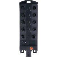
CR2041 - 工业自动化 IFM - 免费用户手册
免费查找设备手册 CR2041 IFM PDF格式.


用户关于以下问题的提问 CR2041 IFM
0 问题 关于此设备。回答您知道的问题或提出自己的问题。
提出关于此设备的新问题
下载您的设备说明 工业自动化 免费PDF格式!查找您的手册 CR2041 - IFM 并重新掌握您的电子设备。本页发布了使用您的设备所需的所有文档。 CR2041 品牌 IFM.
用户手册 CR2041 IFM
CE
操作说明
IO控制模块
CR2040
CR2041
CR2042

目录
1 初步说明 4
1.1 符号说明 4
2 安全说明 …… 5
3 功能和特性 5
4 功能....6
5 安装....6
5.1 安装位置....6
5.2 安装表面....6
5.3 固定 7
5.4 电缆密封件 ..... 7
6 电气连接....8
6.1 配线 8
6.2 一般配线信息 ..... 8
6.3 连接技术....9
6.4 连接附件.... 10
6.5 频率输入..... 10
6.6 反极性保护 ..... 10
6.7 输入端信号发生器的供电 10
6.8 执行器与输出端的连接 ..... 10
6.9 保险丝....10
6.10 连接类型示例 ..... 12
6.10.1 CR2040 12
6.10.2 CR2041 13
6.10.3 CR2042 14
7 操作和显示元件.... 15
7.1 菜单结构.... 16
7.2 输入/输出的状态表示(I/O LED,黄色).... 17
8 设定..... 18
8.1 I/O 模块 18
8.1.1 显示模式..... 18
8.1.2 参数设定..... 18
8.1.3 参数列表..... 20
8.2 控制器..... 20
8.2.1 编程 20
8.3 所需文档.... 20
8.4 所需硬件 20
9 技术资料.... 21
9.1 CR2040 21
9.2 CR2041 28
9.3 CR2042 35
10 维护、修理及处理.... 43
11 认证/标准 43
12 Appendix.... 44
12.1 EMCY Object 44
12.2 Object directory CR204x 45
12.2.1 Device-specific CR2040.... 48
12.2.2 Device-specific CR2041....69
12.2.3 Device-specific CR2042....93
12.3 SDOs error messages 125
12.3.1 CR2040 125
12.3.2 CR2041 127
12.3.3 CR2042 129
1 初步说明
如需技术资料、认证、附件和详细信息,请访问www.ifm.com。
1.1 符号说明
▷ 说明
反应,结果
[...] 按键、按钮或指示标记
→ 交叉引用

重要说明
如不遵守,可能导致故障或干扰。

信息
补充说明

警告!
严重人身伤害警告。可能导致死亡或严重的永久性伤残。

小心!
人身伤害警告可能导致轻微的可逆伤害。
注意!
财产损失警告.
2 安全说明
- 所述设备为集成至系统的子组件。制造商需为系统的安全负责。系统制造商根据运营商和系统用户提供的法规和规范要求来实施风险评估和存档。该存档必须包含针对运营商和用户(如适用,还要包含系统制造商授权的维修人员)的所有必要信息和安全说明。
- 设定产品前请阅读本文档,并在产品整个使用周期内妥善保管本文档。
- 产品必须适合相应的应用和环境条件,且不受任何限制。
- 仅将产品用于指定用途 (→ 3 功能和特性)。
- 如果未遵照操作说明或技术资料,则可能导致人身伤害和/或财产损失。
- 若装置发生故障,请联系制造商。请勿擅自改装本装置。
- 必须由获得相关活动授权的合格人员执行产品的安装、电气连接、设置、编程、配置、操作及维护工作。
- 防止产品、连接器和电缆损坏。
- 损坏设备请予以更换,否则技术资料与安全将无法确保。
注意!
由于焊接造成的过电流、焊渣与脏污
▷ 对装置造成损害,降低电气安全性
▶ 对底盘架构的焊接工作仅可由合格人员执行。
▶ 卸下并覆盖电池的正负端子.
▶ 在车辆或装置上焊接前,将装置的所有触点与车载系统断开连接。
▶ 将焊接装置的接地端子直接连接至要焊接的部件。
▶ 请勿用焊接装置的焊接电极或接地端子触摸装置或电缆。
▶ 保护装置(包括所有连接器与连接电缆)不受焊渣和脏污影响。
3 功能和特性
“ioControl”系列可自由编程的控制器符合艰难条件下使用的规格:如此包含更大的温度范围、可承受更强振动、更大 EMC 干扰和潮湿环境。
使用应用程序软件,用户可配置输入和输出以满足应用需求。控制器可用作CANopen装置、主站或智能I/O模块(→9技术资料)。
与模块化 ioControl 和 Basic 设计的产品结合使用,可实现特定应用的扩展和调整。

警告!
安全功能劣化
▷ 可能存在人员或安装的潜在危险
该装置不允许用于操作员保护领域中与安全相关的任务。
▶ 仅可在技术资料限制范围内使用装置( → 9 技术资料)。
4 功能
- 用户可通过符合 IEC 61131-3 的编程系统 CODESYS 2.3 来轻松创建应用程序软件。装置交付时预先配置为 CANopen 装置。
- 2个CAN接口
- 可配置输入/输出
- 状态 LEDs、I/O LED 和 4 位 10 段显示屏
- 操作键
如需详细信息与配件,请访问 www.ifm.com。
5 安装
5.1 安装位置
容许的安装位置如下:
- 厢体内侧
- 主体
- 车辆车架
不允许安装于发动机上。
对于非移动应用,适用的指令必须遵循,还需考虑指定的环境条件。
5.2 安装表面

外壳不得承受任何扭转力或机械应力。
▶ 将装置安装于平坦表面上。使用合适的补偿元件。
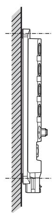


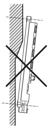
安装表面
5.3 固定
▶ 将随附的空心铆钉从装置后侧插入 3 个固定孔中。
- ▶ 使用 3 个垫圈和 M5 螺丝固定装置。轮流拧紧螺丝。
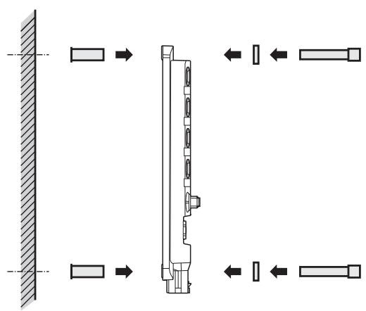

空心铆钉的使用
拧紧扭矩为:2.0 Nm 孔眼尺寸( → 9 技术资料)
| 要使用的螺丝(示例): | 标准 |
| 带六角形凹头的圆柱螺丝(M5 x L) | DIN EN ISO 4762 |
| 带内六角和矮头的圆柱螺丝(M5 x L) | DIN 7984 |
5.4 电缆密封件

在安装之前和安装过程中,请注意污染程度(→9 技术资料),直到通过连接器/堵头确保防护等级为止。防护等级 IP 65 / IP 67 仅可在所有端口均使用连接器或堵头方式密封情况下方可保证。

设备的间隙尺寸可能会有所不同。
6 电气连接

▶ 在安装前,请将设备从主电源上断开;如有必要,也请断开独立供电的输出负载电路。
▶ 遵守有关电气设备安装的国内和国际法规。
▶ 请注意 IEC EN 60204 相关要求。
装置可触及的表面采取符合 IEC 61010-1 的基本绝缘与电路隔绝(二次回路的电压最高为 32 V DC,主电路供电电源能耐 300 V 的过电压,类别 II 电压)。
外部配线必须以确保与其他电路所需隔绝的方式进行。
6.1 配线
接线 ( → 9 技术资料)

连接终端的信号必须符合技术手册规定和/或设备标签指定,符合 ifm electronic 认证的附件也可以连接。

该装置的供电采用通过移动车载系统设计(12/24 V DC 标称电压)或根据技术资料和国家规定采用 SELV/PELV。供电直接传送至连接的传感器/执行器,没有电气隔离。
6.2 一般配线信息
供电电缆和 CAN2 接口通过装置底侧的 X1 连接器来连接。输入/输出、CAN1 接口和 CAN 供电通过外壳前方的 M12 连接器连接。
接线 ( → 9 技术资料)

1: 连接 8
2:连接6
3:连接4
4:连接2
5: CAN1 OUT
6:X1-电源连接器连接
7 : CAN1 IN
8:连接1
9:连接3
10:连接5
11:连接7
连接器区域
| 连接 | CR2040 | CR2041 | CR2042 | 针数 |
| 1 | IN00 / IN08 | OUT00 / OUT08 | IN00 / IN04 | 5 |
| 2 | IN01 / IN09 | OUT01 / OUT09 | OUT00 / OUT04 | 5 |
| 3 | IN02 / IN10 | OUT02 / OUT10 | IN01 / IN05 | 5 |
| 4 | IN03 / IN11 | OUT03 / OUT11 | OUT01 / OUT05 | 5 |
| 5 | IN04 / IN12 | OUT04 / OUT12 | IN02 / IN06 | 5 |
| 6 | IN05 / IN13 | OUT05 / OUT13 | OUT02 / OUT06 | 5 |
| 7 | IN06 / IN14 | OUT06 / OUT14 | IN03 / IN07 | 5 |
| 8 | IN07 / IN15 | OUT07 / OUT15 | OUT03 / OUT07 | 5 |
| CAN1 IN | CAN1 接口 | 5 | ||
| CAN1 OUT | CAN1 接口(如用于回路) | 5 | ||
| X1 | 供电与 CAN2 接口 | 6 | ||

错误的连接方式可能会导致损坏装置。
▶ 遵守安全说明 ( → 2)。
6.3 连接技术
▶ 一般而言,所有电源和信号电缆必须单独敷设。
▶ 使用可能的最短路线,将电源和信号电缆敷设于远离装置处。
▶ 注意装置标签。
▶ 使用带镀金触点的 M12 连接器。
- ▶ 装置中的 M12 连接部件符合 EN 61076-2-101 标准。为确保符合 EN 60529 的防护等级和侵入防护,必须使用通过 EN 61076-2-101 标准的电缆。系统制造商承诺确保由他们切割成一定长度的电缆的侵入防护。
▶ 根据电缆制造商的指示进行固定。最大可允许 3 Nm。
▶ 在安装过程中,请将 M12 连接器垂直放置,令连接螺母不致损伤螺纹。
▶ M12 连接器最大弯矩:4 Nm.
▶ 用保护盖覆盖未使用的插座。拧紧扭矩: 0.8 ± 0.1 Nm
▶ CAN 连接采用双绞线电缆。
▶ 在电缆接口后方出线留400mm,为引出电缆释放应力。
6.4 连接附件
有关可用附件的信息,请访问 www.ifm.com。
6.5 频率输入
CR2040 / CR2042:
▶ 通过屏蔽电缆操作频率输入,以便让有用的信号不会受到外部干扰的影响。
6.6 反极性保护
注意!
缺乏反极性保护
反极性保护仅可在通过车载系统(通过电池)供电时确保,仅限供电机型整体反转(电池连接错误)。反极性造成过电流时,上游保险丝快速关闭即反极性保护的基本原理。若通过 SELV/PELV 供电,反极性保护将无法确保。
▷ 对装置的损坏
▶ 在将连接器连接至装置前,确保电缆末端均适当连接至连接器,同时注意车载系统供电。
6.7 输入端信号发生器的供电
CR2040 / CR2042:
- 使用对应连接器的传感器电压 VBB s 作为输入端信号发生器(如开关或传感器)的供电。
▶ 如输入(开关或传感器)通过外部电压供电,则请保护供电电流不得超过 3 A。
6.8 执行器与输出端的连接
CR2041 / CR2042:
通过 M12 连接器 GND 连接(插脚 3)的总电流不得超过 4 A。如有必要,连接器两个输出(插脚 2 和插脚 4)的负载分配必须进行对应调整。
6.9 保险丝
▶ 必须保护各条独立电路,以便保护整个系统。
| 标记 | 电位 | 连接器:插脚 | 保险丝 | |
| VBBS | 电源传感器/模块 | 8...32 V DC | AMP 连接器:插脚 4 | CR2040: 3 ACR2042: 3 A |
| VBB1 | 电源输出CR2040: 不可用CR2041: OUT00, 02, 04, 06, 08, 10, 12, 14CR2042: 不可用 | 8...32 V DC | AMP 连接器:插脚 4 | CR2040: -CR2041: ≤ 25 ACR2042: - |
| VBB2 | 电源输出CR2040: 不可用CR2041: OUT01, 03, 05, 07, 09, 11, 13, 15CR2042: OUT00...07 | 8...32 V DC | AMP 连接器:插脚 6 | CR2040: -CR2041: ≤ 25 ACR2042: ≤ 25 A |
| VCAN | 可选供电 CAN1 接口CR2040: 已连接至 VBBSCR2041: 未连接至 VBBSCR2042: 已连接至 VBBS | 8...32 V DC | CAN IN: 插脚 2+3 | CR2040: -CR2041: 3 ACR2042: - |
请将属于供电的接地针脚( GND1 、 GND2 ,如适用 GNDCAN )连接至公用接地。
CN
6.10 连接类型示例
6.10.1 CR2040
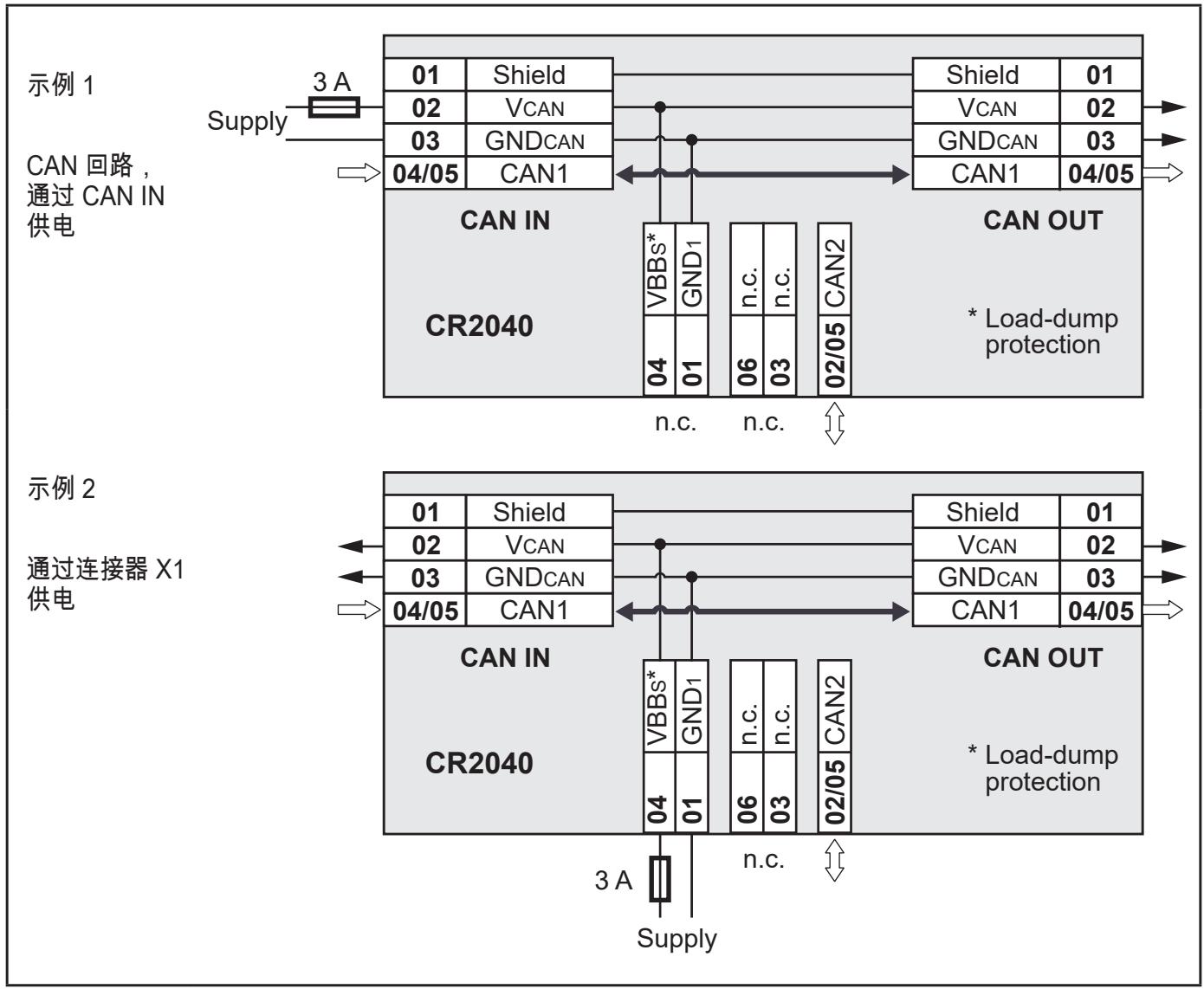
6.10.2 CR2041
针对车载系统过电压的防护仅可在连接 VBBs/VBB1 受到至少 15 A(示例 3)防护或所有供电电压均通过普通保险丝(示例 1 和 2)进行防护的情况下,方可确保。
6.10.3 CR2042
针对车载系统过电压的防护仅可在连接 VBB2 受到至少 15 A(示例 3)防护或所有供电电压均通过普通保险丝(示例 1 和 2)进行防护的情况下,方可确保。
7 操作和显示元件

指示器
1: I/O LED (黄色)
2:电源 LED(绿色)
3:模式 LED(绿色)
4:应用 LED A... LEDD(绿色)
5:锁定 LED(绿色)
6:诊断 LED(红色)
7:4位10段显示屏
10 段显示屏( → 9 技术资料)

操作元件
1: UP 按钮
2:DOWN 按钮
3:ENTER 按钮
按钮功能( → 8.1 I/O 模块)。

手动操作用操作元件
不允许使用带尖头的工具进行操作。按钮可能受损,从而影响防护等级。

灌注混合物可能会对 10 段显示器的视野产生不利影响。

显示屏显示亮度可能有所差异。
7.1 菜单结构

以下对菜单结构的描述遵照 I/O 模块的出厂设定。若装置配置为控制器,则必须定义对应的菜单结构(请参见编程手册 ioControl)。
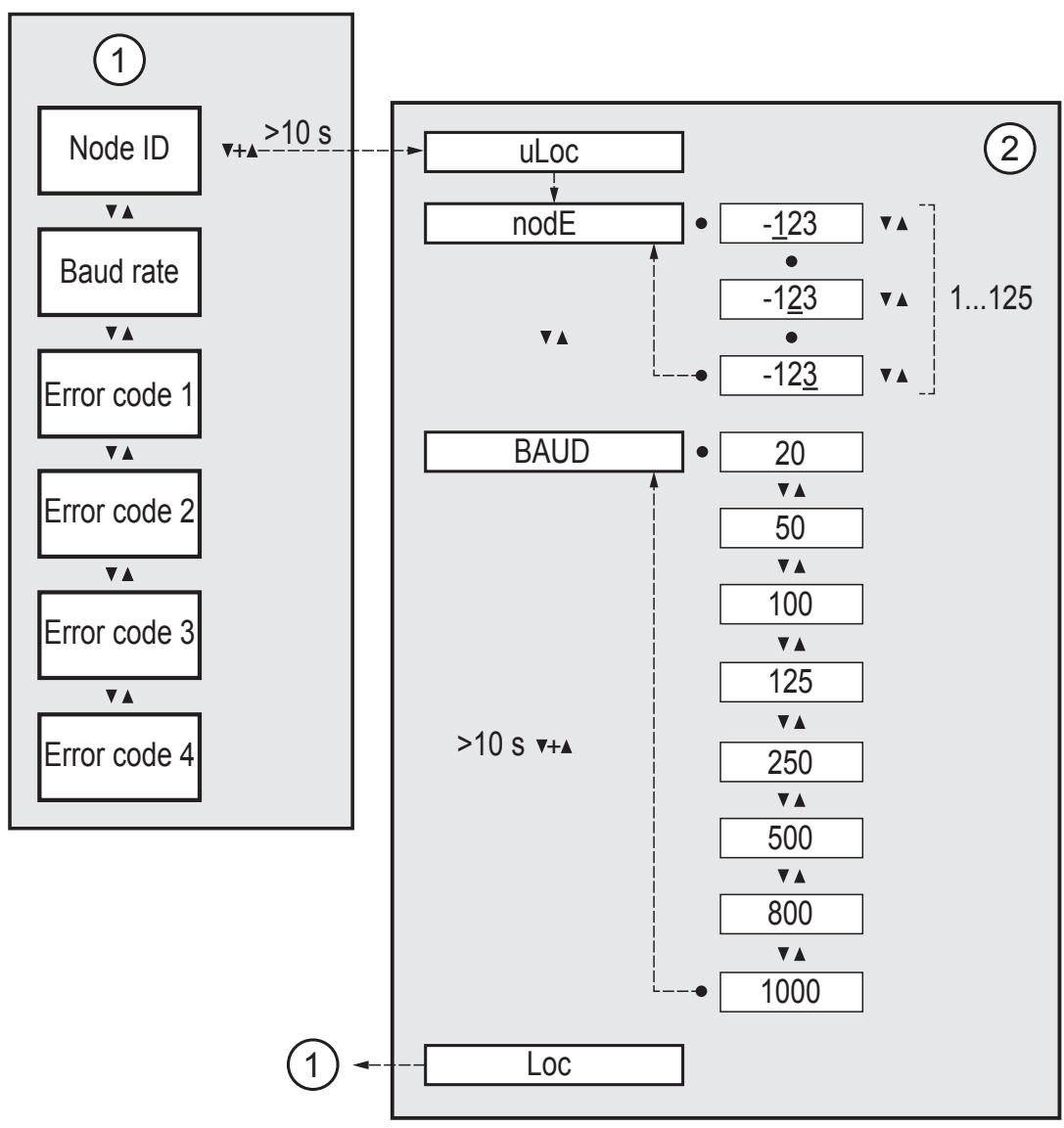
1: 显示模式( → 8.1.1)
2: 编辑模式( → 8.1.2)
参数列表: (→ 8.1.3)
7.2 输入/输出的状态表示(I/O LED,黄色)
| I/O 配置(请参见随附的对象目录) | 状态 LED | µÄ ÷ |
| 0(未使用) | 熄灭 | |
| 1(数字输入 BL) | 熄灭 | 输入信号 FALSE |
| 亮起 | 输入信号 TRUE | |
| 2(数字输出 BH) | 熄灭 | 输出信号 FALSE |
| 亮起 | 输出信号 TRUE | |
| 3(电压输入 10 V) | 熄灭 | |
| 4(PWM 输出) | 熄灭 | PWM 值 = 0‰ |
| 亮起 | PWM 值 = 0‰ | |
| 5(电流控制输出) | 熄灭 | 电流值 ≤ 70 mA |
| 亮起 | 电流值 > 70 mA | |
| 6(电压输入 32 V,比率计) | 熄灭 | |
| 7(电流输入 20 mA) | 熄灭 | |
| 2 Hz | 输入端故障 | |
| 9(电压输入 32 V) | 熄灭 | |
| 10(数字输入 BL) | 熄灭 | 输入信号 FALSE |
| 亮起 | 输入信号 TRUE | |
| 11(数字输入 BL,带有诊断) | 熄灭 | 输入信号 FALSE |
| 亮起 | 输入信号 TRUE | |
| 2 Hz | 输入端故障 | |
| 12(数字输入 BH) | 熄灭 | 输入信号 FALSE |
| 亮起 | 输入信号 TRUE | |
| 14(频率输入) | 熄灭 | |
| 2 Hz | 输入端故障 | |
| 15(数字输出 BH,带有诊断) | 熄灭 | 输出信号 FALSE |
| 亮起 | 输出信号 TRUE | |
| 2 Hz | 输出端故障 | |
| 16(数字输出 BH,带有诊断,短路及过载保护) | 熄灭 | 输出信号 FALSE |
| 亮起 | 输出信号 TRUE | |
| 2 Hz | 输出端故障 | |
| 18(电阻器输入) | 熄灭 | |
| 2 Hz | 输入端故障 | |
| 20(间隔测量) | 熄灭 | |
| 2 Hz | 输入端故障 |
8 设定
8.1 I/O 模块
交付时,装置配置为 I/O 模块。
开启电源后,10 段显示屏会显示装置的产品编号,随后显示节点 ID。
8.1.1 显示模式
如果绿色锁定 LED 亮起,装置处于显示模式。装置仅可指示设定节点 ID、波特率,并在适用时错误信息;▷ 显示无法编辑的参数。
▶ 按 DOWN 按钮。
▷ 装置显示设定波特率。
▶ 按 DOWN 按钮。
▷ 如有适用,装置将显示故障代码 1。
▶ 再按一次 DOWN 按钮。
▶ 使用 UP 按钮返回。▷ 每次按下 DOWN 按钮,如适用,装置会显示另一故障代码。
最多可发生并显示 4 种不同故障代码:
| 错误代码 | 描述 |
| UBB2 | 无电源电压 |
| SH | 对 GND 短路 |
| OP | 断路 |
| LF | 频率输入,频率太低 |
| oC | 输入电流,电流太高 |
| oL | 过电流 |
| IP | 参数设定不正确 |
| Comm | 通信错误 |
| HrTB | Heart beat 错误 |
| mEmr | 内存错误 |
| SYnC | 同步错误 |
如果 10 秒内没有使用按钮,装置会显示设定节点 ID。
8.1.2 参数设定
▶ 同时按下 UP 和 DOWN 按钮至少 10 秒,可更改为编辑模式。
▷ 绿色锁定 LED 熄灭。
▷ 参数可以编辑。
▷ "uLoc" 显示 5 秒▷ 显示 "nodE"
▶ 按 ENTER 按钮。
▷ 装置显示设定节点 ID。
▷ 待编辑的首位闪烁。
▶ 使用 UP 和 DOWN 按钮设定所需的数值。
▶ 使用 ENTER 按钮前进到下一位。
▷ 待编辑的第 2 位闪烁。
▶ 使用 UP 和 DOWN 按钮设定所需的数值。
▶ 使用 ENTER 按钮前进到下一位。
▷ 待编辑的第 3 位闪烁。
▶ 使用 UP 和 DOWN 按钮设定所需的数值。
▶ 按 ENTER 按钮。
▷ 设定节点 ID 已确认。
▷ 显示 "nodE"
▶ 按 DOWN 按钮。
▷ 显示 "BAUD"。
▶ 按 ENTER 按钮。
▷ 装置显示设定波特率。
▶ 使用 UP 和 DOWN 按钮设定所需的数值。
▶ 按 ENTER 按钮。
▷ 设定波特率已确认。

参数更改须在装置重启后方会应用。
退出编辑模式:
▶ 同时按住 UP 和 DOWN 至少 10 秒。
绿色锁定 LED 亮起。
显示无法编辑的参数。
▷ "Loc" 显示 5 秒,随后显示设定节点 ID

如果 30 秒内没有使用按钮,装置会自动结束编辑模式。
8.1.3 参数列表
| 参数 | 功能 | 值范围 | 默认值 |
| nodE | 装置节点 ID | 1...125 | 125 |
| BAUD | 波特率 | 20, 50, 100, 125, 250, 500, 800, 1000 kbit/s | 250 kbit/s |
8.2 控制器
装置可配置为控制器。现有菜单结构和I/O模块属性将丢失。
8.2.1 编程
用户可通过符合 IEC 61131-3 的编程系统 CODESYS 2.3 来轻松创建应用程序软件。

用户应对其自行创建的应用程序的安全功能负责。如有必要,必须请相应的监管和测试机构,按照国家法规额外执行批准程序。

如果需要用作 CANopen 装置时设定 CAN ID 与波特率的说明,请参阅系统手册。
8.3 所需文档
除 CODESYS V2.3 编程系统外,需要以下文档来执行装置的编程和设定:
- 编程手册 CODESYS V2.3
- 系统手册 ioControl
手册可从互联网下载。www.ifm.com
8.4 所需硬件
如果用作移动控制器,需要用于连接至电脑或笔记本的 CAN 接口,以将应用程序加载至装置。
示例:
• CAN/RS232 USB 接口 CANfox (EC2112)
- 适用于 CANfox 的适配器电缆 (EC1213)
您可在以下位置找到有关可用附件的更多信息:www.ifm.com
9 技术资料
9.1 CR2040
CR2040
I/O 模块
数字和模拟
适用于R360系统
CANopen设备
移动控制器
编程标准:IEC 61131-3
16路输入,2路CAN总线接口
8...32 V DC
CE


1: 确认按钮
2:上/下按钮
3:10 段显示屏
4:AMP 连接器
输入电阻
机械数据
外壳
尺寸(高×宽×深)
安装
连接
输入
CAN1 接口
工作电压,CAN2
防护等级
工作/贮藏温度
最大允许相对湿度
最高海拔
污染等级
重量
电气参数
工作电压
耗电量
过电压、电压过低检测
电压过低关闭
处理器
内存(总计)
内存分配
模块控制系统\可用作 CANopen 设备或智能I/O模块
| 外壳:PA6/6.6显示:PA按钮:硅 |
| 234 x 76 x 37 mm(不含空心铆钉) |
| 通过符合 DIN EN ISO 4762 或 DIN 7984 标准的 3 个 M5 螺丝、符合 DIN 7340 的 3 个空芯铆钉以及符合 DIN 7092 标准的 3 个垫圈来固定(已随附空心铆钉和垫圈) |
| 电源供应器:MCP2.8 6 针,用于 TE-AMP 1745078-1 连接器输入/输出:M12,5针触点:AMP: CuFe 镀锡;M12: CuZn (镀金) |
| 8 x 5 针2 x 5 针1 x 6 针 |
IP 65 和 IP 67(所有连接器都安装)
-40...85°C / -40...85°C
90%,无冷凝
2000 m
2
450 g
8...32 V DC
105 mA ( 于 24 V DC ) / 188 mA ( 于 12 V DC ) / 最大 300 mA
36V, t ≤ 10 s
UB ≤ 7.8 V时
UB < 7V 时
飞思卡尔 PowerPC, 50 MHz
592 kbytes RAM / 1536 kbytes 闪存 / 1 kbyte FRAM
编程手册 ioControl 和
www.ifm.com
CR2040
设备监控
CAN 接口 1 和 2
波特率
通信协议
软件/编程
编程系统
输入
配置
指示灯
I/O LED
电源 LED (PWR)
模式 LED (M)
应用 LED (A... D)
锁定 LED(锁形符号)
诊断 LED (DIA)
显示
作为移动控制器使用时的工作状态
技术资料
电压过低监控
电子狗功能
程序和系统的校验和测试
过温监控
CAN 接口 2.0 A/B, ISO 11898
20 Kbit/s...1 Mbit/s ( 默认 CAN1 : 250 kBit/s , CAN2 : 250 kBit/s )
CANopen , CiA DS 301 V4 , CiA DS 401 V1.4
或 SAE J 1939 或自由协议
CODESYS V2.3(IEC 61131-3)
16(可配置)
| 数目 | 设计 | |
| 8 | 开关量,适用于正/负极性传感器信号模拟量(0...10/32 V DC,0...20 mA,比率计) | BL/BHA |
| 4 | 开关量,适用于正极性传感器信号电阻测量(0.016...30 kΩ) | BLR |
| 4 | 开关量,适用于正极性传感器信号开关量,适用于负极性传感器信号*,频率信号(≤30kHz) | BLBHFRQ |
*是指作为I/O模块(CANopen设备)使用时不可用
16 x 橙色 LED
(默认设定:相应输入的状态指示
LED 绿色
(默认设定: 指示系统状态)
LED 绿色
(默认设定: 表示节点 ID 已显示)
4 x 绿色 LED
1 x 绿色 LED
(默认设定: 设定参数的锁定)
1 x 红色 LED
(默认设定: 错误指示)
4 位 10 段显示屏(双色:红色/绿色)
(默认设定: 指示波特率或节点 ID)
| LED | 状态 | 说明 |
| - | 常暗 | 无工作电压 |
| PWR + DIA | 1 x on | 初始化或复位检查 |
| PWR | 5 Hz | 未加载操作系统 |
| 2 Hz | 应用程序运行中 (RUN) | |
| 永久亮起 | 应用程序已停止(停止) | |
| DIA | 10 Hz | 应用程序已停止(停止,有错误) |
| 5 Hz | 因电压过低,应用程序已停止 | |
| 常亮 | 系统错误(严重错误) |
CR2040
操作元件
按钮
按钮(默认设置)
输入特性
模拟量输入 (BL, BH, A)
IN00 - 连接 1, 针脚 2
IN01 - 连接 2, 针脚 2
IN02 - 连接 3, 针脚 2
IN03 - 连接 4, 针脚 2
IN04 - 连接 5, 针脚 2
IN05 - 连接 6, 针脚 2
IN06 - 连接 7, 针脚 2
IN07 - 连接 8, 针脚 2
可被配置为...
开关量输入 (BL, R)
IN08 - 连接 1,针脚 4
IN10 - 连接 3,针脚 4
IN12 - 连接 5,针脚 4
IN14 - 连接 7,针脚 4
可被配置为...
| 技术资料 | |
| ENTER, UP, DOWN | |
| CAN ID / 波特率设定 | |
| ●电压输入 | |
| 输入电压 | 0...10 V或0...32 V |
| 分辨率 | 12位 |
| 精度 | ±1% FS |
| 输入电阻 | 65.6 kΩ (0...10 V), 50.7 kΩ (0...32 V) |
| 输入频率 | ≤500 Hz |
| ●电流输入,带诊断功能 | |
| 输入电流 | 0...20 mA |
| 分辨率 | 12位 |
| 精度 | ±1% FS |
| 输入电阻 | 400 Ω |
| 输入频率 | ≤500 Hz |
| 电流>23 mA时,输入功能将切换至电压输入! | |
| ●电压输入,0...32 V,比率计 | |
| 功能 | (UIN÷UB)×1000‰ |
| 值范围 | 0...1000‰ |
| 输入电阻 | 50.7 kΩ |
| ●正极性传感器信号的开关量电压输入 | |
| 开启电平 | >0.7 UB |
| 关闭电平 | <0.3 UB |
| 输入电阻 | 3.2 kΩ |
| 输入频率 | 50 Hz |
| 诊断断路 | >0.95 UB |
| 诊断短路 | <1 V |
| ●负极性传感器信号的开关量电压输入 | |
| 开启电平 | >0.7 UB |
| 关闭电平 | <0.3 UB |
| 输入电阻 | 3.2 kΩ |
| 输入频率 | 50 Hz |
| 诊断断路 | >0.95 UB |
| 诊断短路 | <1 V |
| ●电阻输入 | |
| 测量范围 | 0.016...30 kΩ |
| 精度 | ±2% FS: 16 Ω...3 kΩ±5% FS: 3...15 kΩ±10% FS: 15...30 kΩ |
CR2040
频率输入 (BL, BH, FRQ)
IN09 - 连接 2 , 针脚 4
IN11 - 连接 4,针脚 4
IN13 - 连接 6 ,针脚 4
IN15 - 连接 8,针脚 4
可被配置为...
CAN 供电 + 传感器电源 VCAN + VBBS 最大总电流
技术资料
| ●频率输入 | |
| 输入电阻 | 3.2 kΩ |
| 输入频率 | ≤ 30 kHz |
| 开启电平 | >0.7 UB |
| 关闭电平 | < 0.3 UB |
| ●正极性传感器信号的开关量电压输入 | |
| 开启电平 | >0.7 UB |
| 关闭电平 | < 0.3 UB |
| 输入电阻 | 3.2 kΩ |
| 输入频率 | 50 Hz |
| 诊断断路* | >0.95 UB |
| 诊断短路* | < 1 V |
| ●负极性传感器信号的开关量电压输入* | |
| 开启电平 | >0.7 UB |
| 关闭电平 | < 0.3 UB |
| 输入电阻 | 3.2 kΩ |
| 输入频率 | 50 Hz |
*表示作为I/O模块使用(Canopen从站)时不可用
1.5 A
| CR2040 | 技术资料 | |
| 测试标准和法规 | ||
| CE 标志 | EN 61000-6-2 | 电磁兼容性 (EMC)抗噪性 |
| EN 61000-6-4 | 电磁兼容性 (EMC)辐射干扰 | |
| E1 标记 | UN/ECE-R10 | 辐射干扰100 V/m 抗扰 |
| ISO 7637-2 | 脉冲 1 ,严重级别:IV ;功能状态 C脉冲 2a ,严重级别:IV ;功能状态 A脉冲 2b ,严重级别:IV ;功能状态 C脉冲 3a ,严重级别:IV ;功能状态 A脉冲 3b ,严重级别:IV ;功能状态 A脉冲 4 ,严重级别:IV ;功能状态 B脉冲 5 ,严重级别:III ;功能状态 C(对于 24V 系统,数据有效)脉冲 4 ,严重级别:III ;功能状态 C(对于 12V 系统,数据有效) | |
| 气候试验 | EN 60068-2-30 | 湿热,循环上限温度 55°C,循环数:6 |
| EN 60068-2-78 | 湿热,稳态测试温度 40°C/93% 相对湿度,测试时长:21 天 | |
| 机械测试 | ISO 16750-3 | 测试 VII ;振动,随机安装位置:车身 |
| EN 60068-2-6 | 振动,正弦10...500 Hz; 0.72 mm/10 g; 10 个循环/轴 | |
| ISO 16750-3 | 撞击30 g/6 ms; 24,000 次冲击 | |
| 耐化学性 | ISO 16750-5 | AA, BA, BD, CC, DB, DC, DD,一次仅允许一种化学品 |
| 备注 | 欧盟合规性声明和认证可在以下位置找到:www.ifm.com | |
CR2040
技术资料
配线
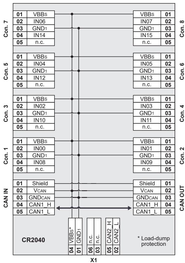
M12插座,5个插针,A-译码
(Con. 1...8, CAN OUT)

M12接插件,5个插针,A-译码
(CAN IN)

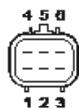
AMP插头
(X1)
| CR2040 | 技术资料 |
| LED分配 | 1: LED IN072: LED IN153: LED IN054: LED IN135: LED IN036: LED IN117: LED IN018: LED IN099: LED IN0810: LED IN0011: LED IN1012: LED IN0213: LED IN1214: LED IN0415: LED IN1416: LED IN06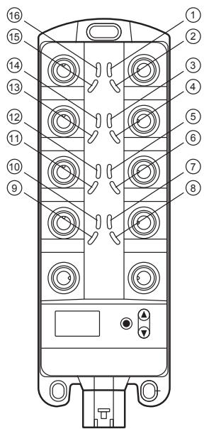 |
| 缩写 | A 模拟BH 二进制高侧BL 二进制低侧FRQ 频率/脉冲输入R 电阻输入VBBS 传感器/模块电源VCAN CAN连接器电源 |
9.2 CR2041
CR2041
I/O模块
数字和模拟
适用于R360系统
CANopen设备
移动控制器
编程标准IEC 61131-3
16路输入,2路CAN总线接口
8...32 V DC
CE
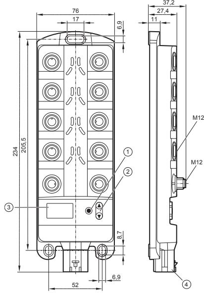
E1
1: 确认按钮
2:上/下按钮
3:10 段显示屏
4:AMP 连接器
技术资料
机械数据
外壳
尺寸(高 x 宽 x 深)
安装
连接
输出
CAN1 接口
工作电压,CAN2
防护等级
工作/贮藏温度
最大允许相对湿度
最高海拔
污染等级
重量
电气参数
工作电压
耗电量
过电压、电压过低检测
电压过低关闭
处理器
内存(总计)
内存分配
模块控制系统\可用作 CANopen 设备或智能I/O模块
| 外壳:PA6/6.6显示:PA按钮:硅 |
| 234 x 76 x 37 mm(不含空心铆钉) |
通过符合 DIN EN ISO 4762 或 DIN 7984 标准的 3 个 M5 螺丝、符合 DIN 7340 的 3 个空芯铆钉以及符合 DIN 7092 标准的 3 个垫圈来固定(已随附空心铆钉和垫圈)
电源供应器: MCP2.8 6 针,用于 TE-AMP 1745078-1 连接器
输入/输出:M12,5针
触点:AMP: CuFe 镀锡;M12: CuZn (镀金)
8×5针
2×5针
1×6针
IP 65 和 IP 67(所有连接器都安装)
-40...85°C / -40...85°C
90%,无冷凝
2000 m
2
450 g
8...32 V DC
105 mA (于 24 V DC) / 188 mA (于 12 V DC) / 最大 300 mA
36V, t ≤ 10 s
UB ≤ 7.8 V时
UB < 7V 时
飞思卡尔 PowerPC,50 MHz
592 kbytes RAM / 1536 kbytes 闪存 / 1 kbyte FRAM
编程手册 ioControl 和
www.ifm.com
CR2041
设备监控
CAN 接口 1 和 2
波特率
通信协议
软件/编程
编程系统
输出
配置
指示灯
I/O LED
电源 LED (PWR)
模式 LED (M)
应用 LED (A... D)
锁定 LED(锁形符号)
诊断 LED (DIA)
显示
作为移动控制器使用时的工作状态
技术资料
电压过低监控
电子狗功能
程序和系统的校验和测试
过温监控
CAN 接口 2.0 A/B,ISO 11898
20 Kbit/s...1 Mbit/s ( 默认 CAN1 : 250 kbit/s, CAN2: 250 kbit/s)
CANopen, CiA DS 301 V4, CiA DS 401 V1.4
或 SAE J 1939 或自由协议
CODESYS V2.3(IEC 61131-3)
16(可配置)
| 数目 | 设计 | |
| 4 | 正极性开关(高电平),4A,诊断PWM输出(20...250 Hz),4A,诊断电流控制0.02...4A | BHPWMWPMI |
| 4 | 正极性开关(高电平),2.5A,诊断PWM输出(20...250 Hz),2.5A,诊断电流控制0.02A | BHPWMWPMI |
| 4 | 正极性开关(高电平),4A,诊断PWM输出(20...250 Hz),4A | BHPWM |
| 4 | 正极性开关(高电平),2.5A,诊断PWM输出(20...250 Hz),2.5A | BHPWM |
16 x 橙色 LED
(默认设定: 相应输出的状态指示
LED 绿色
(默认设定: 指示系统状态)
LED 绿色
(默认设定: 表示节点 ID 已显示)
4 x 绿色 LED
1 x 绿色 LED
(默认设定: 设定参数的锁定)
1 x 红色 LED
(默认设定: 错误指示)
4 位 10 段显示屏(双色:红色/绿色)
(默认设定: 指示波特率或节点 ID)
| LED | 状态 | 说明 |
| - | 常暗 | 无工作电压 |
| PWR + DIA | 1 x on | 初始化或复位检查 |
| PWR | 5 Hz | 未加载任何操作系统 |
| 2 Hz | 应用程序运行中 (RUN) | |
| 常亮 | 应用程序已停止(停止) | |
| DIA | 10 Hz | 应用程序已停止(停止,有错误) |
| 5 Hz | 因电压过低,应用程序已停止 | |
| 永久亮起 | 系统错误(严重错误) |
CR2041
操作元件
按钮
按钮(默认设置)
输出特性
开关量输出 (BH, PWM, PWMI)
OUT00 - 连接 1,插脚 4
OUT01 - 连接 2,插脚 4
OUT02 - 连接 3,插脚 4
OUT03 - 连接 4,插脚 4
可被配置为...
开关量输出(BH,PWM,PWMI)
OUT04-连接5,针脚4
OUT05-连接6,针脚4
OUT06-连接7,针脚4
OUT07-连接8,针脚4
可配置为:
技术资料
ENTER, UP, DOWN
CAN ID / 波特率设定
| 半导体输出,正极性输出(高电平侧),防短路和过载保护.通过电流反馈诊断(断线/过载).通过电压反馈诊断,可以解除上拉电阻(断线/短路)。 | |
| 开关电压 | 8...32 V |
| 开关电流 | 0.02...4 A |
| 负载电阻 | ≥ 3Ω (12 V DC时) ≥ 6Ω (24 V DC时) |
| 当前测量范围 | 0.02...6 A |
| 反馈电流的精度 | 1% FS |
| PWM输出 | |
| 输出频率 | 20...250 Hz |
| 脉冲/占空比 | 1...1000‰ |
| 开关电流 | 0.02...4 A |
| 当前测量范围 | 0.02...6 A |
| 反馈电流的精度 | 3% FS |
| 电流控制输出 | |
| 输出频率 | 20...250 Hz |
| 控制范围 | 0.02...4 A |
| 设定分辨率 | 1 mA |
| 最大浪涌电流 | ≤ 24 A |
| 反馈电流的精度 | 3% FS |
| 半导体输出,正极性输出(高电平侧),防短路和过载保护.通过电流反馈诊断(断线/过载).通过电压反馈诊断,可以解除上拉电阻(断线/短路)。 | |
| 开关电压 | 8...32 V |
| 开关电流 | 0.02...2.5 A |
| 负载电阻器 | ≥ 4.8 Ω (12 V DC) ≥ 9.6 Ω (24 V DC) |
| 当前测量范围 | 0.02...4 A |
| 反馈电流的精度 | 1 % FS |
| PWM 输出 | |
| 输出频率 | 20...250 Hz |
| 脉冲/占空比 | 1...1000 ‰ |
| 开关电流 | 0.02...2.5 A |
| 当前测量范围 | 0.02...4 A |
| 反馈电流的精度 | 3 % FS |
| 电流控制输出 | |
| 输出频率 | 20...250 Hz |
| 控制范围 | 0.02...2.5 A |
| 设定分辨率 | 1 mA |
| 最大浪涌电流 | ≤ 24 A |
| 反馈电流的精度 | 3 % FS |
CR2041
开关量输出(BH,PWM)
OUT08-连接1,针脚2
OUT09-连接2,针脚2
OUT10-连接3,针脚2
OUT11-连接4,针脚2
可配置为:
开关量输出(BH,PWM)
OUT12-连接5,针脚2
OUT13-连接6,针脚2
OUT14-连接7,针脚2
OUT15-连接8,针脚2
可配置为:
续流二极管
过载保护
(对于所有输出功能有效)
短路保护
(对于所有输入和输出功能有效)
VCAN的最大总电流
输出连接器每个 GND 、(pin 3)最大总电流
输出电源 VBB1 / VBB2 的最大总电流
技术资料
| ●半导体输出,正极性输出(高电平侧),防短路和过载保护.通过电压反馈诊断,可以解除上拉电阻(断路/短路)。 | |
| 开关电压 | 8...32 V |
| 开关电流 | 0.02...2.5 A |
| ● PWM 输出 | |
| 输出频率 | 20...250 Hz |
| 脉冲/占空比 | 1...1000 % |
| 开关电流 | 0.02...2.5 A |
| 最大浪涌电流 | ≤ 24 A |
| ●半导体输出,正极性输出(高电平侧),防短路和过载保护.通过电压反馈诊断,可以解除上拉电阻(断线/短路)。 | |
| 开关电压 | 8...32 V |
| 开关电流 | 0.02...4 A |
| ● PWM 输出 | |
| 输出频率 | 20...250 Hz |
| 脉冲/占空比 | 1...1000 % |
| 开关电流 | 0.02...4 A |
| 最大浪涌电流 | ≤ 24 A |
集成有抑制感性负载的续流二极管
≤ 5 分钟(100% 过载时)
≤ 5 分钟
1.5 A
4.0 A

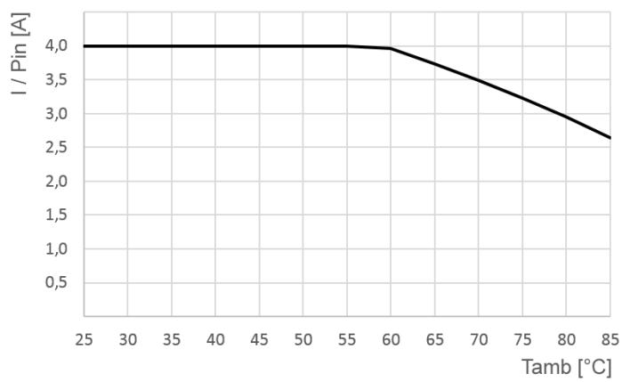
1: 安装在车辆外部(有外部对流)
2: 安装在控制柜内的金属板上
3: 安装在导热系数低的表面上(如塑料或木材)
CR2041
M12 连接器每个插脚的最大电流负载(连续电流负载)
技术资料
测试标准和法规
CE 标志
E1 标记
气候试验
机械测试
耐化学性
备注
EN 61000-6-2 电磁兼容性 (EMC) 抗噪性
EN 61000-6-4 电磁兼容性 (EMC) 辐射干扰
UN/ECE-R10 辐射干扰 100 V/m 抗扰
ISO 7637-2 脉冲 1,严重级别:IV;功能状态 C 脉冲 2a,严重级别:IV;功能状态 A 脉冲 2b,严重级别:IV;功能状态 C 脉冲 3a,严重级别:IV;功能状态 A 脉冲 3b,严重级别:IV;功能状态 A 脉冲 4,严重级别:IV;功能状态 B 脉冲 5,严重级别:III;功能状态 C (对于 24V 系统,数据有效) 脉冲 4,严重级别:III;功能状态 C (对于 12V 系统,数据有效)
EN 60068-2-30 湿热,循环 上限温度 55° C,循环数:6
EN 60068-2-78 湿热,稳态 测试温度 40° C/93% 相对湿度, 测试时长:21 天
ISO 16750-3 测试 VII;振动,随机安装位置:车身
EN 60068-2-6 振动,正弦 10...500 Hz; 0.72 mm/10 g; 10 个循环/轴
ISO 16750-3 撞击 30 g/6 ms; 24,000 次冲击
ISO 16750-5 AA, BA, BD, CC, DB, DC, DD, 一次仅允许一种化学品
欧盟合规性声明和认证可在以下位置找到:www.ifm.com
CR2041
技术资料
配线

M12插座,5个插针,A-译码(Con. 1...8, CAN OUT)

M12接插件,5个插针,A-译码(CAN IN)

AMP插头 (X1)
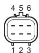
| CR2041 | 技术资料 |
| LED分配 | 1: LED OUT152: LED OUT073: LED OUT134: LED OUT055: LED OUT116: LED OUT037: LED OUT098: LED OUT019: LED OUT0010: LED OUT0811: LED OUT0212: LED OUT1013: LED OUT0414: LED OUT1215: LED OUT0616: LED OUT14 |
| 缩写 | BH 二进制高侧BL 开关量低电平侧PWM 脉冲宽度调制PWMI 脉冲宽度调制,电流控制VBBS 电源传感器/模块VBB1 OUT00, OUT02, OUT04, OUT06, OUT08, OUT10, OUT12, OUT14 电源VBB2 OUT01, OUT03, OUT05, OUT07, OUT09, OUT11, OUT13, OUT15 电源VCAN CAN 连接器电源 |
ifm electronic gmbh • Friedrichstraße 1 • 45128 Essen
我们保留事先不予通知,即执行技术改造的权利!
CR2041 / 页码 7 02/09/2024
9.3 CR2042
CR2042
输入/输出模块
数字和模拟
适用于R360系统
CANopen设备
移动控制器
IEC 61131-3
编程
8 个输入
8 个输出
2 个 CAN 接口
8...32 V DC
CE


1: ENTER 按钮
2:UP/DOWN 按钮
3:10 段显示屏
4:AMP 连接器
技术资料
机械数据
外壳
尺寸(高 x 宽 x 深)
安装
连接
输入
输出
CAN1 接口
工作电压,CAN2
防护等级
工作/贮藏温度
最大允许相对湿度
最高海拔
污染程度
重量
电气数据
工作电压
耗电量
过电压、电压过低检测
电压过低关闭
处理器
内存(总计)
内存分配
模块控制系统\可用作 CANopen 装置或智能输入/输出模块
| 外壳:PA6/6.6显示:PA按钮:硅 |
| 234 x 76 x 37 mm(不含空心铆钉) |
| 通过符合DIN EN ISO 4762或DIN 7984标准的3个M5螺丝、符合DIN 7340的3个空芯铆钉以及符合DIN 7092标准的3个垫圈来固定(已随附空心铆钉和垫圈) |
| 电源供应器:MCP2.8 6针,用于TE-AMP 1745078-1连接器输入/输出:M12,5针触点:AMP:CuFe镀锡;M12:CuZn(镀金) |
| 4 x 5针4 x 5针2 x 5针1 x 6针 |
| IP 65和IP 67(所有连接器都安装) |
| -40...85°C/-40...85°C |
| 90%,无冷凝 |
| 2000 m |
| 2 |
| 450 g |
| 8...32 V DC |
| 105 mA(于24 V DC)/188 mA(于12 V DC)/最大300 mA |
| 36V,t≤10 sUB≤7.8 V时UB<7V时 |
| 飞思卡尔 PowerPC,50 MHz |
| 592 kbytes RAM/1536 kbytes闪存/1 kbyte FRAM |
| 编程手册 ioControl 和www.ifm.com |
CR2042
装置监控
CAN 接口 1 和 2
波特率
通信协议
软件/编程
编程系统
输入
配置
输出
配置
指示灯
I/O LED
电源 LED (PWR)
模式 LED (M)
应用 LED (A... D)
锁定 LED(锁形符号)
诊断 LED (DIA)
显示
技术资料
电压过低监控
电子狗功能
程序和系统的校验和测试
过温监控
CAN 接口 2.0 A/B, ISO 11898
20 Kbit/s...1 Mbit/s ( 默认 CAN1 : 250 kbit/s, CAN2: 250 kbit/s)
CANopen,CiA DS 301 版本 4,CiA DS 401 版本 1.4
或 SAE J 1939 或自由协议
CODESYS 2.3 版本 (IEC 61131-3)
8(可配置)
| 数目 | 设计 | |
| 4 | 数字,适用于正/负极性传感器信号模拟(0...10/32 V DC,0..20 mA,比率计)频率(≤30 kHz) | BL/BHAFRQ |
| 4 | 数字,适用于正极性传感器信号电阻测量(0.016...30 kΩ) | BLR |
8(可配置)
| 数目 | 设计 | |
| 4 | 正极性开关(高电平),4A,诊断PWM输出(20...250 Hz),4A,诊断电流控制0.02...4A | BHPWMWPMI |
| 4 | 正极性开关(高电平),2.5A,诊断PWM输出(20...250 Hz),2.5A,诊断电流控制0.02A | BHPWMWPMI |
16 x 橙色 LED
(默认设定:对应输入/输出的状态指示)
LED 绿色
(默认设定: 指示系统状态)
LED 绿色
(默认设定: 表示节点 ID 已显示)
4 x 绿色 LED
1 x 绿色 LED
(默认设定: 设定参数的锁定)
1 x 红色 LED
(默认设定: 错误诊断)
4 位 10 段显示屏 ( 双色 : 红色/绿色 )
(默认设定: 指示波特率或节点 ID )
CR2042
作为移动控制器使用时为工作状态
操作元件
按钮
按钮(默认设置)
输入特性
模拟量输入 (BL, BH, A, FRQ)
IN00 - 连接 1,插脚 2
IN01 - 连接 3,插脚 2
IN02 - 连接 5,插脚 2
IN03 - 连接 7,插脚 2
可被配置为...
技术资料
| LED | 状态 | ˵à ÷ |
| - | 永久关闭 | 无工作电压 |
| PWR + DIA | 1 x 开启 | 初始化或复位检查 |
| PWR | 5 Hz | 未加载任何操作系统 |
| 2 Hz | 应用程序运行中 (RUN) | |
| 永久亮起 | 应用程序已停止(停止) | |
| DIA | 10 Hz | 应用程序已停止(停止,但有错误) |
| 5 Hz | 因电压过低,应用程序已停止 | |
| 永久亮起 | 系统错误(严重错误) |
ENTER, UP, DOWN
CAN ID / 波特率设定
| ●电压输入 | |
| 输入电压 | 0...10V或0...32V |
| 分辨率 | 12位 |
| 精度 | ±1%FS |
| 输入电阻 | 65.6kΩ(0...10V),50.7kΩ(0...32V) |
| 输入频率 | ≤500Hz |
| ●电流输入,带有诊断功能 | |
| 输入电流 | 0...20mA |
| 分辨率 | 12位 |
| 精度 | ±1%FS |
| 输入电阻 | 400Ω |
| 输入频率 | ≤500Hz |
| 电流>23mA时,输入功能将切换至电压输入! | |
| ●电压输入,0...32V,比率计 | |
| 功能 | (UIN÷UB)x1000‰ |
| 值范围 | 0...1000‰ |
| 输入电阻 | 50.7kΩ |
| ●正极性传感器信号的开关量电压输入 | |
| 开启电平 | >0.7UB |
| 关闭电平 | <0.3UB |
| 输入电阻 | 3.2kΩ |
| 输入频率 | 50Hz |
| 诊断断路 | >0.95UB |
| 诊断短路 | <1V |
| ●负极性传感器信号的开关量电压输入 | |
| 开启电平 | >0.7UB |
| 关闭电平 | <0.3UB |
| 输入电阻 | 3.2kΩ |
| 输入频率 | 50Hz |
| ●频率输入 | |
| 输入电阻 | 3.2kΩ |
| 输入频率 | ≤30kHz |
| 开启电平 | >0.7UB |
| 关闭电平 | <0.3UB |
CR2042
开关量输入 (BL, R)
IN04 - 连接 1,插脚 4
IN05 - 连接 3,插脚 4
IN06 - 连接 5,插脚 4
IN07 - 连接 7,插脚 4
可被配置为...
输出特性
开关量输出 (BH, PWM, PWMI)
OUT00 - 连接 2,插脚 4
OUT01 - 连接 4,插脚 4
OUT02 - 连接 6,插脚 4
OUT03 - 连接 8,插脚 4
可被配置为...
技术资料
| ●正极性传感器信号的开关量电压输入 | |
| 开启电平 | >0.7 UB |
| 关闭电平 | <0.3 UB |
| 输入电阻 | 3.2 kΩ |
| 输入频率 | 50 Hz |
| 诊断断路 | >0.95 UB |
| 诊断短路 | <1 V |
| ●电阻输入 | |
| 测量范围 | 0.016...30 kΩ |
| 精度 | ±2% FS: 16 Ω...3 kΩ±5 % FS: 3...15 kΩ±10 % FS: 15...30 kΩ |
| 半导体输出,正极性输出(高电平侧),防短路和过载保护。通过电流反馈诊断(断线/过载)。通过电压反馈诊断,可以解除上拉电阻(断线/短路)。 | |
| 开关电压 | 8...32 V |
| 开关电流 | 0.02...4 A |
| 负载电阻器 | ≥ 3Ω (12 V DC时) ≥ 6Ω (24 V DC时) |
| 当前测量范围 | 0.02...6 A |
| 反馈电流的精度 | 1% FS |
| PWM 输出 | |
| 输出频率 | 20...250 Hz |
| 脉冲/占空比 | 1...1000‰ |
| 开关电流 | 0.02...4 A |
| 当前测量范围 | 0.02...6 A |
| 反馈电流的精度 | 3% FS |
| 电流控制输出 | |
| 输出频率 | 20...250 Hz |
| 控制范围 | 0.02...4 A |
| 设定分辨率 | 1 mA |
| 最大浪涌电流 | ≤ 24 A |
| 反馈电流的精度 | 3% FS |
CR2042
模拟输入 (BH, PWM, PWMI)
OUT04 - 连接 2,插脚 2
OUT05 - 连接 4,插脚 2
OUT06 - 连接 6,插脚 2
OUT07 - 连接 8,插脚 2
可被配置为...
反向保护继流二极管
过载保护
(对于所有输出功能有效)
短路保护
(对于所有输入和输出功能有效)
CAN 供电 + 传感器电源 VCAN + VBBS 最大总电流
输出连接器每个 GND 、(pin 3)最大总电流
输出电源 VBB2 的最大总电流
技术资料
| ●半导体输出,正极性输出(高电平侧),防短路和过载保护.通过电流反馈诊断(断线/过载).通过电压反馈诊断,可以解除上拉电阻(断线/短路)。 | |
| 开关电压 | 8...32 V |
| 开关电流 | 0.02...2.5 A |
| 负载电阻器 | ≥ 4.8 Ω (12 V DC) ≥ 9.6 Ω (24 V DC) |
| 当前测量范围 | 0.02...4 A |
| 反馈电流的精度 | 1 % FS |
| ●PWM 输出 | |
| 输出频率 | 20...250 Hz |
| 脉冲/占空比 | 1...1000 ‰ |
| 开关电流 | 0.02...2.5 A |
| 当前测量范围 | 0.02...4 A |
| 反馈电流的精度 | 3 % FS |
| ●电流控制输出 | |
| 输出频率 | 20...250 Hz |
| 控制范围 | 0.02...2.5 A |
| 设定分辨率 | 1 mA |
| 最大浪涌电流 | ≤ 24 A |
| 反馈电流的精度 | 3 % FS |
集成有钝化感性负载的续流二极管
≤ 5 分钟(100% 过载时)
≤ 5 分钟
1.5 A
4.0 A

1: 安装在车辆外部(有外部对流)
2: 安装于控制柜内金属板上或导热系数低的表面(如塑料或木材)上
CR2042
M12 连接器每个插脚的最大电流负载(连续电流负载)
技术资料
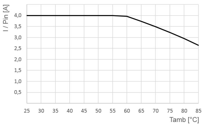
测试标准和法规
CE 标志
E1 标记
气候试验
机械测试
耐化学性
备注
EN 61000-6-2 电磁兼容性 (EMC) 抗噪性
EN 61000-6-4 电磁兼容性 (EMC) 辐射干扰
UN/ECE-R10 辐射干扰 100 V/m 抗扰
ISO 7637-2 脉冲 1,严重级别:IV;功能状态 C 脉冲 2a,严重级别:IV;功能状态 A 脉冲 2b,严重级别:IV;功能状态 C 脉冲 3a,严重级别:IV;功能状态 A 脉冲 3b,严重级别:IV;功能状态 A 脉冲 4,严重级别:IV;功能状态 B 脉冲 5,严重级别:III;功能状态 C (对于 24V 系统,数据有效) 脉冲 4,严重级别:III;功能状态 C (对于 12V 系统,数据有效)
EN 60068-2-30 湿热,循环 上限温度 55° C,循环数:6
EN 60068-2-78 湿热,稳态 测试温度 40° C/93% 相对湿度, 测试时长:21 天
ISO 16750-3 测试 VII;振动,随机安装位置:车身
EN 60068-2-6 振动,正弦 10...500 Hz; 0.72 mm/10 g; 10个循环/轴 ISO 16750-3 撞击 30 g/6 ms; 24,000次冲击 ISO 16750-5 AA, BA, BD, CC, DB, DC, DD, 一次仅允许一种化学品
欧盟合规性声明和认证可在以下位置找到:www.ifm.com
CR2042
配线
技术资料

M12插座,5个插针,A-译码(Con. 1...8, CAN OUT)

M12接插件,5个插针,A-译码(CAN IN)

AMP插头(X1)

| CR2042 | 技术资料 |
| LED分配 | 1: LED OUT072: LED OUT033: LED OUT064: LED OUT025: LED OUT056: LED OUT017: LED OUT048: LED OUT009: LED IN0410: LED IN0011: LED IN0512: LED IN0113: LED IN0614: LED IN0215: LED IN0716: LED IN03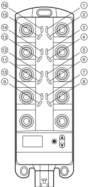 |
| 缩写 | A 模拟量R 电阻输入FRQ 频率/脉冲输入BH 开关量高电平侧BL 开关量低电平侧PWM 脉冲宽度调制PWMI 脉冲宽度调制,电流控制VBBS 电源传感器/模块VBB2 供电OUT01... OUT07VCAN 供应CAN连接器 |
10 维护、修理及处理
装置无需维护.
▶ 请勿打开外壳,因为装置不含可由用户维护的任何组件。仅可由制造商修理装置。

更换装置时,请注意污染程度(→9 技术资料),直到通过连接器/堵头确保防护等级为止。如有必要,请在更换前对装置 / 连接器进行清洁。请检查连接器密封可重用性。防护等级仅在密封完整时可以确保。
▶ 请使用干布清洁装置。

以下化学剂不适用清洁装置:溶解塑料的化学品,诸如异丙醇、甲基化酒精、汽油、稀释剂、乙醇、丙酮或氨水。
▶ 按照国家环保法规处理产品。
11 认证/标准
测试标准和法规( → 9 技术资料)
欧盟合规性声明和认证可在以下位置找到:www.ifm.com
12 Appendix
12.1 EMCY Object
The following error codes according to DSP-401 or DSP-301 are supported:
| EMCY code | Error reg | Additional code | Description |
| 0x6100 | 0x11 | 0x00 | "Internal Software Overflow of an Rx queue e.g. frequency of the RxP-DOs is too high. Reset only externally via entry in the index 0x1003 Subldx 00." |
| 0x6101 | 0x11 | 0x00 | "Internal Software Overflow of an Tx queue e.g. device does not communicate with the bus. Reset only externally via entry in the index 0x1003 Subldx 00." |
| 0x8000 | 0x11 | 0x00 | "Monitoring Sync Error For communication cycle no sync object is received. Only in Operational. Reset with the next sync OBJ or PREOP" |
| 0x8100 | 0x11 | 0x00 | Communication Err |
| 0x8131 | 0x11 | 0x00 | "Monitoring Heart Beat ErrorNo guard object is received. Reset with the next Heart beat or PREOP" |
| 0x63xx | 0x01 | 0x00 | "Invalid parameter of an input or output.""xx"" means number of the IO-channel (00 ... 15)" |
| 0x5000 | 0x01 | 0x00 | Memory Error |
| 0x3308 | 0x05 | 0x00 | VBB2 error (only CR2041, CR2042) |
| 0x90xx | 0x01 | 0x00 | "Frequency input, Frequency too low""xx"" means number of the IO-channel (00 ... 15)" |
| 0x21xx | 0x03 | 0x00 | "Inputs, Openline""xx"" means number of the IO-channel (00 ... 15)" |
| 0x21xx | 0x03 | 0x00 | "Inputs, Short circuit""xx"" means number of the IO-channelCR2040 (00 ... 15) + 16; CR2042 (00 ... 07) + 8" |
| 0x21xx | 0x03 | 0x00 | "Inputs, Overcurrent""xx"" means number of the IO-channelCR2040 (00 ... 15) + 32; CR2042 (00 ... 07) + 16" |
| 0x23xx | 0x03 | 0x00 | "outputs, Openline""xx"" means number of the IO-channelCR2041 (00 ... 15); CR2042 (00 ... 07)" |
| 0x23xx | 0x03 | 0x00 | "outputs, Short circuit""xx"" means number of the IO-channelCR2041 (00 ... 15) + 16; CR2042 (00 ... 07) + 8" |
| 0x23xx | 0x03 | 0x00 | "outputs, Overload""xx"" means number of the IO-channelCR2041 (00 ... 15) + 32; CR2042 (00 ... 07) + 16" |
CANopen does not provide for two identical EMCY objects to be sent consecutively.
12.2 Object directory CR204x
Obligatory objects (index 0x1000...0x1FFF):
| Index | S-idx | Designation | Data type | Default | Details | |
| 0x1000 | Device type | ro | UDINT | 0x000F0191 | Device type | |
| 0x1001 | Error register | ro | USINT | 0 | Error register bitcoded to profile 301 Permissible values:0b0000 0000 = no error0b0000 0001 = generic error0b0001 0000 = communication error0b1000 0000 = manufacturer specific | |
| 0x1018 | 0x00 | Device identification Number of entries | ro | USINT | 0x04 | Device identification |
| 0x01 | Vendor-ID | ro | UDINT | 0x0069666D | Vendor ID oft he device according to CiA specification | |
| 0x02 | Product code | ro | STRING | 0 | Product code of the device | |
| 0x03 | Revision number | ro | UDINT | 0 | Revision number of the device | |
| 0x04 | Serial number | ro | UDINT | 0 | Serial number of the device | |
| 0x1003 | 0x00 | Predefined error field Number of entries | rw | UDINT | 0 | An error list with 4 entries is supported |
| 0x01 | Error history | ro | UDINT | 0 | Error occurred, coded according to EMCY list The last error is indicated in the sub-index 1 | |
| 0x02 | Error history | ro | UDINT | 0 | Error occurred, coded according to EMCY list | |
| 0x03 | Error history | ro | UDINT | 0 | Error occurred, coded according to EMCY list | |
| 0x04 | Error history | ro | UDINT | 0 | Error occurred, coded according to EMCY list | |
| 0x05 | Error history | ro | UDINT | 0 | Error occurred, coded according to EMCY list | |
| 0x1005 | COB-ID synch message | rw | UDINT | 0x0000 0080 | Identifier of the synch message Bit 30 = 0 → device generates no synch message Bit 30 = 1 → device generates a synch message Bit 29 = 0 → 11 bit IDBit 29 = 1 → ID = 0x80 + node ID | |
| 0x1006 | Communi-cation cycle period | rw | UDINT | 0 | Max. time between 2 synch objects in [μs] Control resolution = 1 ms | |
| 0x1008 | Manufacturer device name | ro | STRING | CR204x | Device designation (CR2040 or CR2041 or CR2042) | |
| 0x1009 | Manufacturer hardware version | ro | STRING | V00.00.00 | Hardware version | |
| 0x100A | Manufacturer software version | ro | STRING | V00.00.00 | Software version | |
| 0x1010 | 0x00 | Store para-meters Largest sub-index supported | ro | USINT | 0x01 | Number of "save options" |
| 0x01 | Save all parameters | rw | UDINT | 2 | Automatic saving of all parameters changed0 = AutoSave OFF2 = AutoSave ON | |
| 0x1011 | 0x00 | Restore default parameters Largest sub-index supported | ro | USINT | 0x01 | Number of "restore options" |
| 0x01 | Restore all default parameters | rw | UDINT | 0x01 | If the String "load" is entered here, the default parameters set at the factory are restored and become valid after the next reset. | |
| 0x1014 | COBId Emergency | rw | UDINT | 0x80 + node ID | Bit 31 = 0 → EMCY is valid Bit 31 = 1 → EMCY is not valid Bit 29 = 0 → 11-bit IDBit 29 = 1 → ID = 0x80 + node IDCAN identifier can be changed by the user. | |
| 0x1016 | 0x00 | Consumer heartbeat times Nums consumer heartbeat time | ro | USINT | 0x01 | Heartbeat monitoring time for the node Number of devices monitored = 1 |
| 0x01 | Consumer heartbeat time | rw | UDINT | 0 | Heartbeat monitoring time for the node Format: 0x0nntttttttt = monitoring time [ms]nn = node numberif nn=0 or tttt=0 → no monitoring | |
| 0x1017 | Producer heartbeat time | rw | UINT | 0 | Time intervall [ms] during which the device generates a producer heartbeat | |
12.2.1 Device-specific CR2040
Transmit PDO communication parameters (index 0x1800...0x18FF):
| Index | S-idx | Designation | Data type | Default | Details | |
| 0x1800 | 0x00 | Transmit PDO Communication Parameter Number of entries | ro | USINT | 0x05 | Configuration transmit PDO 1 number of entries = 5 |
| 0x01 | COBID used by PDO | rw | UDINT | 0x180 + Node ID | CAN ID of the transmit PDO 1 Bit 31 = 0 → PDO is valid Bit 31 = 1 → PDO is not valid | |
| 0x02 | transmission type | rw | USINT | 0xFF | 0x00 = synch acyclic 0x01...0xF0 = synch cyclic; values are only transmitted after „n" synch objects n = 1...240 = 0x01...0xF0 0xFC/0xFD not implemented 0xFE = asynch man. spec. event; values are immediately transferred 0xFF = asynch device profile event; values are immediately transferred | |
| 0x03 | inhibit time | rw | UINT | 0 | delay time in the transmission type "asynch" before the PDO is transmitted again at the earliest. (0...65535 • 100 μs) | |
| 0x04 | reserved | rw | USINT | 0 | reserve | |
| 0x05 | event time | rw | UINT | 0 | max. transfer break in the transmission type „asynch" (0...65535 ms) When this time has elapsed, the PDO is transferred even if the appl. event has not accrued. | |
| 0x1801 | 0x00 | Transmit PDO Communication Parameter Number of entries | ro | USINT | 0x05 | Configuration transmit PDO 2 number of entries = 5 |
| 0x01 | COBID used by PDO | rw | UDINT | 0x280 + Node ID | CAN ID of the transmit PDO 2 Bit 31 = 0 → PDO is valid Bit 31 = 1 → PDO is not valid | |
| 0x02 | transmission type | rw | USINT | 0x01 | 0x00 = synch acyclic 0x01...0xF0 = synch cyclic; values are only transmitted after „n" synch objects n = 1...240 = 0x01...0xF0 0xFC/0xFD not implemented 0xFE = asynch man. spec. event; values are immediately transferred 0xFF = asynch device profile event; values are immediately transferred | |
| 0x03 | inhibit time | rw | UINT | 0 | delay time in the transmission type "asynch" before the PDO is transmitted again at the earliest. (0...65535 • 100 μs) | |
| 0x04 | reserved | rw | USINT | 0 | reserve | |
| 0x05 | event time | rw | UINT | 0 | max. transfer break in the transmission type „asynch" (0...65535 ms) When this time has elapsed, the PDO is transferred even if the appl. event has not accrued. | |
| 0x1802 | 0x00 | Transmit PDO Communication Parameter Number of entries | ro | USINT | 0x05 | Configuration transmit PDO 3 number of entries = 5 |
| 0x01 | COBID used by PDO | rw | UDINT | 0x380 + Node ID | CAN ID of the transmit PDO 3 Bit 31 = 0 → PDO is valid Bit 31 = 1 → PDO is not valid | |
| 0x02 | transmission type | rw | USINT | 0x01 | 0x00 = synch acyclic 0x01...0xF0 = synch cyclic; values are only transmitted after „n" synch objects n = 1...240 = 0x01...0xF0 0xFC/0xFD not implemented 0xFE = asynch man. spec. event; values are immediately transferred 0xFF = asynch device profile event; values are immediately transferred | |
| 0x03 | inhibit time | rw | UINT | 0 | delay time in the transmission type "asynch" before the PDO is transmitted again at the earliest. (0...65535 • 100 μs) | |
| 0x04 | reserved | rw | USINT | 0 | reserve | |
| 0x05 | event time | rw | UINT | 0 | max. transfer break in the transmission type „asynch" (0...65535 ms) When this time has elapsed, the PDO is transferred even if the appl. event has not accrued. | |
| 0x1803 | 0x00 | Transmit PDO Communication Parameter Number of entries | ro | USINT | 0x05 | Configuration transmit PDO 4 number of entries = 5 |
| 0x01 | COBID used by PDO | rw | UDINT | 0x480 + Node ID | CAN ID of the transmit PDO 4 Bit 31 = 0 → PDO is valid Bit 31 = 1 → PDO is not valid | |
| 0x02 | transmission type | rw | USINT | 0x01 | 0x00 = synch acyclic 0x01...0xF0 = synch cyclic; values are only transmitted after „n" synch objects n = 1...240 = 0x01...0xF0 0xFC/0xFD not implemented 0xFE = asynch man. spec. event; values are immediately transferred 0xFF = asynch device profile event; values are immediately transferred | |
| 0x03 | inhibit time | rw | UINT | 0 | delay time in the transmission type "asynch" before the PDO is transmitted again at the earliest. (0...65535 • 100 μs) | |
| 0x04 | reserved | rw | USINT | 0 | reserve | |
| 0x05 | event time | rw | UINT | 0 | max. transfer break in the transmission type „asynch" (0...65535 ms) When this time has elapsed, the PDO is transferred even if the appl. event has not accrued. | |
| 0x1804 | 0x00 | Transmit PDO Communication Parameter Number of entries | ro | USINT | 0x05 | Configuration transmit PDO 5 number of entries = 5 |
| 0x01 | COBID used by PDO | rw | UDINT | 0x181 + Node ID | CAN ID of the transmit PDO 5 Bit 31 = 0 → PDO is valid Bit 31 = 1 → PDO is not valid | |
| 0x02 | transmission type | rw | USINT | 0x01 | 0x00 = synch acyclic 0x01...0xF0 = synch cyclic; values are only transmitted after „n" synch objects n = 1...240 = 0x01...0xF0 0xFC/0xFD not implemented 0xFE = asynch man. spec. event; values are immediately transferred 0xFF = asynch device profile event; values are immediately transferred | |
| 0x03 | inhibit time | rw | UINT | 0 | delay time in the transmission type "asynch" before the PDO is transmitted again at the earliest. (0...65535 • 100 μs) | |
| 0x04 | reserved | rw | USINT | 0 | reserve | |
| 0x05 | event time | rw | UINT | 0 | max. transfer break in the transmission type „asynch" (0...65535 ms) When this time has elapsed, the PDO is transferred even if the appl. event has not accrued. | |
| 0x1805 | 0x00 | Transmit PDO Communication Parameter Number of entries | ro | USINT | 0x05 | Configuration transmit PDO 6 number of entries = 5 |
| 0x01 | COBID used by PDO | rw | UDINT | 0x281 + Node ID | CAN ID of the transmit PDO 6 Bit 31 = 0 → PDO is valid Bit 31 = 1 → PDO is not valid | |
| 0x02 | transmission type | rw | USINT | 0x01 | 0x00 = synch acyclic 0x01...0xF0 = synch cyclic; values are only transmitted after „n" synch objects n = 1...240 = 0x01...0xF0 0xFC/0xFD not implemented 0xFE = asynch man. spec. event; values are immediately transferred 0xFF = asynch device profile event; values are immediately transferred | |
| 0x03 | inhibit time | rw | UINT | 0 | delay time in the transmission type "asynch" before the PDO is transmitted again at the earliest. (0...65535 • 100 μs) | |
| 0x04 | reserved | rw | USINT | 0 | reserve | |
| 0x05 | event time | rw | UINT | 0 | max. transfer break in the transmission type „asynch" (0...65535 ms) When this time has elapsed, the PDO is transferred even if the appl. event has not accrued. | |
| 0x1806 | 0x00 | Transmit PDO Communication Parameter Number of entries | ro | USINT | 0x05 | Configuration transmit PDO 7 number of entries = 5 |
| 0x01 | COBID used by PDO | rw | UDINT | 0x381 + Node ID | CAN ID of the transmit PDO 7 Bit 31 = 0 → PDO is valid Bit 31 = 1 → PDO is not valid | |
| 0x02 | transmission type | rw | USINT | 0x01 | 0x00 = synch acyclic 0x01...0xF0 = synch cyclic; values are only transmitted after „n" synch objects n = 1...240 = 0x01...0xF0 0xFC/0xFD not implemented 0xFE = asynch man. spec. event; values are immediately transferred 0xFF = asynch device profile event; values are immediately transferred | |
| 0x03 | inhibit time | rw | UINT | 0 | delay time in the transmission type "asynch" before the PDO is transmitted again at the earliest. (0...65535 • 100 μs) | |
| 0x04 | reserved | rw | USINT | 0 | reserve | |
| 0x05 | event time | rw | UINT | 0 | max. transfer break in the transmission type „asynch" (0...65535 ms) When this time has elapsed, the PDO is transferred even if the appl. event has not accrued. | |
| 0x1807 | 0x00 | Transmit PDO Communication Parameter Number of entries | ro | USINT | 0x05 | Configuration transmit PDO 8 number of entries = 5 |
| 0x01 | COBID used by PDO | rw | UDINT | 0x481 + Node ID | CAN ID of the transmit PDO 8 Bit 31 = 0 → PDO is valid Bit 31 = 1 → PDO is not valid | |
| 0x02 | transmission type | rw | USINT | 0x01 | 0x00 = synch acyclic 0x01...0xF0 = synch cyclic; values are only transmitted after „n" synch objects n = 1...240 = 0x01...0xF0 0xFC/0xFD not implemented 0xFE = asynch man. spec. event; values are immediately transferred 0xFF = asynch device profile event; values are immediately transferred | |
| 0x03 | inhibit time | rw | UINT | 0 | delay time in the transmission type "asynch" before the PDO is transmitted again at the earliest. (0...65535 • 100 μs) | |
| 0x04 | reserved | rw | USINT | 0 | reserve | |
| 0x05 | event time | rw | UINT | 0 | max. transfer break in the transmission type „asynch" (0...65535 ms) When this time has elapsed, the PDO is transferred even if the appl. event has not accrued. | |
| 0x1808 | 0x00 | Transmit PDO Communication Parameter Number of entries | ro | USINT | 0x05 | Configuration transmit PDO 9 number of entries = 5 |
| 0x01 | COBID used by PDO | rw | UDINT | 0x182 + Node ID | CAN ID of the transmit PDO 9 Bit 31 = 0 → PDO is valid Bit 31 = 1 → PDO is not valid | |
| 0x02 | transmission type | rw | USINT | 0x01 | 0x00 = synch acyclic 0x01...0xF0 = synch cyclic; values are only transmitted after „n" synch objects n = 1...240 = 0x01...0xF0 0xFC/0xFD not implemented 0xFE = asynch man. spec. event; values are immediately transferred 0xFF = asynch device profile event; values are immediately transferred | |
| 0x03 | inhibit time | rw | UINT | 0 | delay time in the transmission type "asynch" before the PDO is transmitted again at the earliest. (0...65535 • 100 μs) | |
| 0x04 | reserved | rw | USINT | 0 | reserve | |
| 0x05 | event time | rw | UINT | 0 | max. transfer break in the transmission type „asynch" (0...65535 ms) When this time has elapsed, the PDO is transferred even if the appl. event has not accrued. | |
| 0x1809 | 0x00 | Transmit PDO Communication Parameter Number of entries | ro | USINT | 0x05 | Configuration transmit PDO 10 number of entries = 5 |
| 0x01 | COBID used by PDO | rw | UDINT | 0x282 + Node ID | CAN ID of the transmit PDO 10 Bit 31 = 0 → PDO is valid Bit 31 = 1 → PDO is not valid | |
| 0x02 | transmission type | rw | USINT | 0x01 | 0x00 = synch acyclic 0x01...0xF0 = synch cyclic; values are only transmitted after „n" synch objects n = 1...240 = 0x01...0xF0 0xFC/0xFD not implemented 0xFE = asynch man. spec. event; values are immediately transferred 0xFF = asynch device profile event; values are immediately transferred | |
| 0x03 | inhibit time | rw | UINT | 0 | delay time in the transmission type "asynch" before the PDO is transmitted again at the earliest. (0...65535 • 100 μs) | |
| 0x04 | reserved | rw | USINT | 0 | reserve | |
| 0x05 | event time | rw | UINT | 0 | max. transfer break in the transmission type „asynch" (0...65535 ms) When this time has elapsed, the PDO is transferred even if the appl. event has not accrued. | |
Transmit PDO mapping (index 0x1A00...0x1AFF):
| Index | S-idx | Designation | Data type | Default | Details | |
| 0x1A00 | 0x00 | Transmit PDO mapping Number of mapped objects in PDO | rw | USINT | 0x07 | mapping transmit PDO 1 number of integrated application objects = 7 |
| 0x01 | PDO mapping | rw | UDINT | 0x6000 0108 | Index 0x6000, SubIndex 0x01 binary inputs 00...07: actual values (bit coded) | |
| 0x02 | PDO mapping | rw | UDINT | 0x6000 0208 | Index 0x6000, SubIndex 0x02 binary inputs 08...15: actual values (bit coded) | |
| 0x03 | PDO mapping | rw | UDINT | 0x2020 0108 | Index 0x2020, SubIndex 0x01 binary inputs 00...07: flag "short circuit" (bit coded) | |
| 0x04 | PDO mapping | rw | UDINT | 0x2020 0208 | Index 0x2020, SubIndex 0x02 binary inputs 08...15: flag "short circuit" (bit coded) | |
| 0x05 | PDO mapping | rw | UDINT | 0x2021 0108 | Index 0x2021, SubIndex 0x01 outputs 00...07: flag " wire break " (bit coded) | |
| 0x06 | PDO mapping | rw | UDINT | 0x2021 0208 | Index 0x2021, SubIndex 0x02 outputs 08...15: flag " wire break " (bit coded) | |
| 0x07 | PDO mapping | rw | UDINT | 0x2025 0108 | Index 0x2025, SubIndex 0x01 inputs 00...03: flag " overload " (bit coded) | |
| 0x1A01 | 0x00 | Transmit PDO mapping Number of mapped objects in PDO | rw | USINT | 0x04 | mapping transmit PDO 2 (analogue inputs)number of integrated application objects = 4 |
| 0x01 | PDO mapping | rw | UDINT | 0x6404 0110 | Index 0x6404, SubIndex 0x01 analogue input 00: actual value (depending on the configuration 0x2000) | |
| 0x02 | PDO mapping | rw | UDINT | 0x6404 0210 | Index 0x6404, SubIndex 0x02 analogue input 01: actual value (depending on the configuration 0x2000)) | |
| 0x03 | PDO mapping | rw | UDINT | 0x6404 0310 | Index 0x6404, SubIndex 0x03 analogue input 02: actual value (depending on the configuration 0x2000) | |
| 0x04 | PDO mapping | rw | UDINT | 0x6404 0410 | Index 0x6404, SubIndex 0x04 analogue input 03: actual value (depending on the configuration 0x2000) | |
| 0x1A02 | 0x00 | Transmit PDO mapping Number of mapped objects in PDO | rw | USINT | 0x04 | mapping transmit PDO 3 (analogue inputs)number of integrated application objects = 4 |
| 0x01 | PDO mapping | rw | UDINT | 0x6404 0510 | Index 0x6404, SubIndex 0x05 analogue input 04: actual value (depending on the configuration 0x2000) | |
| 0x02 | PDO mapping | rw | UDINT | 0x6404 0610 | Index 0x6404, SubIndex 0x06 analogue input 05: actual value (depending on the configuration 0x2000)) | |
| 0x03 | PDO mapping | rw | UDINT | 0x6404 0710 | Index 0x6404, SubIndex 0x07 analogue input 06: actual value (depending on the configuration 0x2000) | |
| 0x04 | PDO mapping | rw | UDINT | 0x6404 0810 | Index 0x6404, SubIndex 0x08 analogue input 07: actual value (depending on the configuration 0x2000) | |
| 0x1A03 | 0x00 | Transmit PDO mapping Number of mapped objects in PDO | rw | USINT | 0x04 | mapping transmit PDO 4 number of integrated application objects = 4 |
| 0x01 | PDO mapping | rw | UDINT | 0x2030 0110 | Index 0x2030, SubIndex 0x01 input 08: actual resistor value | |
| 0x02 | PDO mapping | rw | UDINT | 0x2030 0210 | Index 0x2030, SubIndex 0x02 input 10: actual resistor value | |
| 0x03 | PDO mapping | rw | UDINT | 0x2030 0310 | Index 0x2030, SubIndex 0x03 input 12: actual resistor value | |
| 0x04 | PDO mapping | rw | UDINT | 0x2030 0410 | Index 0x2030, SubIndex 0x04 input 14: actual resistor value | |
| 0x1A04 | 0x00 | Transmit PDO mapping Number of mapped objects in PDO | rw | USINT | 0x02 | mapping transmit PDO 5 (periode time IN09, IN11) number of integrated application objects = 2 |
| 0x01 | PDO mapping | rw | UDINT | 0x2012 0120 | Index 0x2012, SubIndex 0x01 frequency input IN09: periode time of the signal | |
| 0x02 | PDO mapping | rw | UDINT | 0x2012 0220 | Index 0x2012, SubIndex 0x02 frequency input IN11: periode time of the signal | |
| 0x1A05 | 0x00 | Transmit PDO mapping Number of mapped objects in PDO | rw | USINT | 0x02 | mapping transmit PDO 6 (periode time IN13, IN15) number of integrated application objects = 2 |
| 0x01 | PDO mapping | rw | UDINT | 0x2012 0320 | Index 0x2012, SubIndex 0x03 frequency input IN13: periode time of the signal | |
| 0x02 | PDO mapping | rw | UDINT | 0x2012 0420 | Index 0x2012, SubIndex 0x04 frequency input IN15: periode time of the signal | |
| 0x1A06 | 0x00 | Transmit PDO mapping Number of mapped objects in PDO | rw | USINT | 0x04 | mapping transmit PDO 7 (duty cycle of the signal on the frequency input IN09, IN11, IN13, IN15) number of integrated application objects = 4 |
| 0x01 | PDO mapping | rw | UDINT | 0x2014 0110 | Index 0x2014, SubIndex 0x01 frequency input IN09: duty cycle of the signal in ‰ | |
| 0x02 | PDO mapping | rw | UDINT | 0x2014 0210 | Index 0x2014, SubIndex 0x02 frequency input IN11: duty cycle of the signal in ‰ | |
| 0x03 | PDO mapping | rw | UDINT | 0x2014 0310 | Index 0x2014, SubIndex 0x03 frequency input IN13: duty cycle of the signal in ‰ | |
| 0x04 | PDO mapping | rw | UDINT | 0x2014 0410 | Index 0x2014, SubIndex 0x04 frequency input IN15: duty cycle of the signal in ‰ | |
| 0x1A07 | 0x00 | Transmit PDO mapping Number of mapped objects in PDO | rw | USINT | 0x02 | mapping transmit PDO 8 (frequency on IN09, IN11) number of integrated application objects = 2 |
| 0x01 | PDO mapping | rw | UDINT | 0x2015 0120 | Index 0x2015, SubIndex 0x01 frequency input IN09: frequency value of the signal in Hz | |
| 0x02 | PDO mapping | rw | UDINT | 0x2015 0220 | Index 0x2015, SubIndex 0x02 frequency input IN11: frequency value of the signal in Hz | |
| 0x1A08 | 0x00 | Transmit PDO mapping Number of mapped objects in PDO | rw | USINT | 0x02 | mapping transmit PDO 9 (frequency on IN13, IN15) number of integrated application objects = 2 |
| 0x01 | PDO mapping | rw | UDINT | 0x2015 0320 | Index 0x2015, SubIndex 0x03 frequency input IN13: frequency value of the signal in Hz | |
| 0x02 | PDO mapping | rw | UDINT | 0x2015 0420 | Index 0x2015, SubIndex 0x04 frequency input IN15: frequency value of the signal in Hz | |
| 0x1A09 | 0x00 | Transmit PDO mapping Number of mapped objects in PDO | rw | USINT | 0x02 | mapping transmit PDO 10 (system flag) number of integrated application objects = 2 |
| 0x01 | PDO mapping | rw | UDINT | 0x2040 0110 | Index 0x2040, SubIndex 0x01 supply voltage of the system VBBS | |
| 0x02 | PDO mapping | rw | UDINT | 0x2050 0010 | Index 0x2050, SubIndex 0x00 system temperature in °C | |
Manufacturer-specific objekts (index 0x2000...0x6FFF):
| Index | S-idx | Designation | Data type | Default | Details | ||
| 0x2000 | 0x00 | IO configuration Largest sub-index supported | ro | USINT | 16 | Configuration inputs/outputs largest supported Sub-index = 32 | |
| 0x01 | Configuration IN00 | rw | USINT | 10 | 0 = 0x003 = 0x036 = 0x067 = 0x079 = 0x0910 = 0x0A11 = 0x0B12 = 0x0C | off Input IN000...10 000 mV ratiometric 0...1000 %o0...20 000 μA0...32 000 mV binary plus switched binary plus switched with diagnosis binary minus switched | |
| 0x02 | Configuration IN01 | rw | USINT | 10 | 0 = 0x003 = 0x036 = 0x067 = 0x079 = 0x0910 = 0x0A11 = 0x0B12 = 0x0C | off Input IN010...10 000 mV ratiometric 0...1000 %o0...20 000 μA0...32 000 mV binary plus switched binary plus switched with diagnosis binary minus switched | |
| 0x03 | Configuration IN02 | rw | USINT | 10 | 0 = 0x003 = 0x036 = 0x067 = 0x079 = 0x0910 = 0x0A11 = 0x0B12 = 0x0C | off Input IN020...10 000 mV ratiometric 0...1000 %o0...20 000 μA0...32 000 mV binary plus switched binary plus switched with diagnosis binary minus switched | |
| 0x2000 | 0x04 | Configuration IN03 | rw | USINT | 10 | 0 = 0x003 = 0x036 = 0x067 = 0x079 = 0x0910 = 0x0A11 = 0x0B12 = 0x0C | off Input IN030...10 000 mV ratiometric 0...1000 %o0...20 000 μA0...32 000 mV binary plus switched binary plus switched with diagnosis binary minus switched |
| 0x05 | Configuration IN04 | rw | USINT | 10 | 0 = 0x003 = 0x036 = 0x067 = 0x079 = 0x0910 = 0x0A11 = 0x0B12 = 0x0C | off Input IN040...10 000 mV ratiometric 0...1000 %o0...20 000 μA0...32 000 mV binary plus switched binary plus switched with diagnosis binary minus switched | |
| 0x06 | Configuration IN05 | rw | USINT | 10 | 0 = 0x003 = 0x036 = 0x067 = 0x079 = 0x0910 = 0x0A11 = 0x0B12 = 0x0C | off Input IN050...10 000 mV ratiometric 0...1000 %o0...20 000 μA0...32 000 mV binary plus switched binary plus switched with diagnosis binary minus switched | |
| 0x07 | Configuration IN06 | rw | USINT | 10 | 0 = 0x003 = 0x036 = 0x067 = 0x079 = 0x0910 = 0x0A11 = 0x0B12 = 0x0C | off Input IN060...10 000 mV ratiometric 0...1000 %o0...20 000 μA0...32 000 mV binary plus switched binary plus switched with diagnosis binary minus switched | |
| 0x08 | Configuration IN07 | rw | USINT | 10 | 0 = 0x003 = 0x036 = 0x067 = 0x079 = 0x0910 = 0x0A11 = 0x0B12 = 0x0C | off Input IN070...10 000 mV ratiometric 0...1000 %o0...20 000 μA0...32 000 mV binary plus switched binary plus switched with diagnosis binary minus switched | |
| 0x09 | Configuration IN08 | rw | USINT | 10 | 0 = 0x0010 = 0x0A11 = 0x0B18 = 0x12 | off Input IN08 binary plus switched binary plus switched with diagnosis 16...30 000 Ohm | |
| 0x2000 | 0x0A | Configuration IN09 | rw | USINT | 01 | 0 = 0x0001 = 0x0114 = 0x0E20 = 0x14 | off Input IN09binary plus switched frequency0...30 000 Hzperiod duration |
| 0x0B | Configuration IN10 | rw | USINT | 10 | 0 = 0x0010 = 0x0A11 = 0x0B18 = 0x12 | off Input IN10binary plus switched binary plus switched with diagnosis16...30 000 Ohm | |
| 0x0C | Configuration IN11 | rw | USINT | 01 | 0 = 0x0001 = 0x0114 = 0x0E20 = 0x14 | off Input IN11binary plus switched frequency0...30 000 Hzperiod duration | |
| 0x0D | Configuration IN12 | rw | USINT | 10 | 0 = 0x0010 = 0x0A11 = 0x0B18 = 0x12 | off Input IN12binary plus switched binary plus switched with diagnosis16...30 000 Ohm | |
| 0x0E | Configuration IN13 | rw | USINT | 01 | 0 = 0x0001 = 0x0114 = 0x0E20 = 0x14 | off Input IN12binary plus switched frequency0...30 000 Hzperiod duration | |
| 0x0F | Configuration IN14 | rw | USINT | 10 | 0 = 0x0010 = 0x0A11 = 0x0B18 = 0x12 | off Input IN14binary plus switched binary plus switched with diagnosis16...30 000 Ohm | |
| 0x10 | Configuration IN15 | rw | USINT | 01 | 0 = 0x0001 = 0x0114 = 0x0E20 = 0x14 | off Input IN15binary plus switched frequency0...30 000 Hzperiod duration | |
| 0x2012 | 0x00 | Period input | ro | USINT | 4 | Largest sub-index supported | |
| 0x01 | Period duration IN09 | ro | UDINT | 0 | IN09 period duration [μs] | ||
| 0x02 | Period duration IN11 | ro | UDINT | 0 | IN11 period duration [μs] | ||
| 0x03 | Period duration IN13 | ro | UDINT | 0 | IN13 period duration [μs] | ||
| 0x04 | Period duration IN15 | ro | UDINT | 0 | IN15 period duration [μs] | ||
| 0x2013 | 0x00 | Period input number of periods for average | ro | USINT | 4 | Largest sub-index supported | |
| 0x01 | Number of periods IN09 | rw | USINT | 4 | 1...255 | IN09 number of periods | |
| 0x02 | Number of periods IN11 | rw | USINT | 4 | 1...255 | IN11 number of periods | |
| 0x03 | Number of periods IN13 | rw | USINT | 4 | 1...255 | IN13 number of periods | |
| 0x04 | Number of periods IN15 | rw | USINT | 4 | 1...255 | IN15 number of periods | |
| 0x2014 | 0x00 | Period input - ratio value | ro | USINT | 4 | Largest sub-index supported | |
| 0x01 | Period ratio value IN09 | ro | UINT | 0 | 0...1 000 | IN09 marc-to-space ratio [%] | |
| 0x02 | Period ratio value IN11 | ro | UINT | 0 | 0...1 000 | IN11 marc-to-space ratio [%] | |
| 0x03 | Period ratio value IN13 | ro | UINT | 0 | 0...1 000 | IN13 marc-to-space ratio [%] | |
| 0x04 | Period ratio value IN15 | ro | UINT | 0 | 0...1 000 | IN15 marc-to-space ratio [%] | |
| 0x2015 | 0x00 | Frequency input | ro | USINT | 4 | Largest sub-index supported | |
| 0x01 | Frequency IN09 | ro | REAL | 1 | 0...30 000 | IN09 frequency [Hz] | |
| 0x02 | Frequency IN11 | ro | REAL | 1 | 0...30 000 | IN11 frequency [Hz] | |
| 0x03 | Frequency IN13 | ro | REAL | 1 | 0...30 000 | IN13 frequency [Hz] | |
| 0x04 | Frequency IN15 | ro | REAL | 1 | 0...30 000 | IN15 frequency [Hz] | |
| 0x2016 | 0x00 | Timebase | ro | USINT | 4 | Largest sub-index supported | |
| 0x01 | Timebase IN09 | rw | UINT | 50 | 0...2 000 | IN09 timebase [ms] | |
| 0x02 | Timebase IN11 | rw | UINT | 50 | 0...2 000 | IN11 timebase [ms] | |
| 0x03 | Timebase IN13 | rw | UINT | 50 | 0...2 000 | IN13 timebase [ms] | |
| 0x04 | Timebase IN15 | rw | UINT | 50 | 0...2 000 | IN15 timebase [ms] | |
| 0x2020 | 0x00 | Input – short to supply voltage | ro | USINT | 2 | Largest sub-index supported | |
| 0x01 | Short to supply voltage IN00... IN07 | ro | USINT | 0 | 0 = normal1 = short circuit | channels (bit coded)0b---- ---X = IN000b---- --X- = IN010b---- -X-- = IN020b---- X--- = IN030b---X ---- = IN040b--X- ---- = IN050b-X-- ---- = IN060bX--- ---- = IN07 | |
| 0x02 | Short to supply voltage IN08, IN10, IN12, IN14 | ro | USINT | 0 | 0 = normal1 = short circuit | channels (bit coded)0b---- ---X = IN080b---- --X- = IN100b---- -X-- = IN120b---- X--- = IN14 | |
| 0x2021 | 0x00 | Input – wire break | ro | USINT | 2 | Largest sub-index supported | |
| 0x01 | Wire break IN00... IN07 | ro | USINT | 0 | 0 = normal1 = wire break | channels (bit coded)0b---- ---X = IN000b---- --X- = IN010b---- -X-- = IN020b---- X--- = IN030b---X ---- = IN040b--X- ---- = IN050b-X-- ---- = IN060bX--- ---- = IN07 | |
| 0x02 | Wire break IN08, IN10, IN12, IN14 | ro | USINT | 0 | 0 = normal1 = wire break | channels (bit coded)0b---- ---X = IN080b---- --X- = IN100b---- -X-- = IN120b---- X--- = IN14 | |
| 0x2025 | 0x00 | Input analog – overcurrent | ro | USINT | 1 | Largest sub-index supported | |
| 0x01 | Overcurrent IN00... IN07 | ro | USINT | 0 | 0 = normal1 = overcurrent | channels (bit coded)0b---- ---X = IN000b---- --X- = IN010b---- -X-- = IN020b---- X--- = IN030b---X ---- = IN040b--X- ---- = IN050b-X-- ---- = IN060bX--- ---- = IN07 | |
| 0x2030 | 0x00 | Input resistor | ro | USINT | 4 | Largest sub-index supported | |
| 0x01 | Resistance IN08 | ro | UINT | 0 | 0...30 000 | IN08 resistance [Ohms] | |
| 0x02 | Resistance IN10 | ro | UINT | 0 | 0...30 000 | IN10 resistance [Ohms] | |
| 0x03 | Resistance IN12 | ro | UINT | 0 | 0...30 000 | IN12 resistance [Ohms] | |
| 0x04 | Resistance IN14 | ro | UINT | 0 | 0...30 000 | IN14 resistance [Ohms] | |
| 0x2040 | 0x00 | System supply voltage VBBS | ro | USINT | 1 | Largest sub-index supported | |
| 0x01 | VBBS | ro | USINT | 0 | VBBS voltage [mV] | ||
| 0x2050 | Device temperature | ro | UINT | 0 | temperature [°C] | ||
| 0x20F0 | Node ID | rw | USINT | 125 | 1...125 | node ID [!] value(0x20F0) != value(20F1) | |
| 0x20F1 | Node ID | rw | USINT | 125 | 1...125 | node ID [!] value(0x20F0) != value(20F1) | |
| 0x20F2 | Baud rate | rw | USINT | 3 | baud rate [!] value(0x20F2) != value(20F3) | ||
| 0 | 1000 kBit/s | ||||||
| 1 | 800 kBit/s | ||||||
| 2 | 500 kBit/s | ||||||
| 3 | 250 kBit/s | ||||||
| 4 | 125 kBit/s | ||||||
| 5 | 100 kBit/s | ||||||
| 6 | 50 kBit/s | ||||||
| 7 | 20 kBit/s | ||||||
| 0x20F3 | Baud rate | rw | USINT | 3 | baud rate [!] value(0x20F2) != value(20F3) | ||
| 0x20F4 | Autostart | rw | UINT | 0 | not used | ||
| 0x20F5 | Lock edit mode | rw | USINT | 0 | 0 = edit mode unlocked1 = edit mode locked | ||
| 0x20F6 | CAN interface | rw | USINT | 1 | 1...2 | CAN interface [!] value(0x20F6) != value(20F7) | |
| 0x20F7 | CAN interface | rw | USINT | 1 | 1...2 | CAN interface [!] value(0x20F6) != value(20F7) | |
| Index | S-idx | Designation | Data type | Default | Details | |
| 0x6000 | 0x00 | Binary input Largest sub-index supported | ro | USINT | 0x02 | Binary inputs Largest supported sub-index = 2 |
| 0x01 | Binary inputs IN00 - IN07 | ro | USINT | 0 | Binary inputs IN00... IN070b---- ---X = IN000b---- --X- = IN010b---- -X-- = IN020b---- X--- = IN030b---X ---- = IN040b--X- ---- = IN050b-X-- ---- = IN060bX--- ---- = IN07 | |
| 0x02 | Binary inputs IN08 - IN15 | ro | USINT | 0 | Binary inputs IN08... IN150b---- ---X = IN080b---- --X- = IN090b---- -X-- = IN100b---- X--- = IN110b---X ---- = IN120b--X- ---- = IN130b-X-- ---- = IN140bX--- ---- = IN15 | |
| 0x6404 | 0x00 | Analogue input Largest sub-index supported | ro | USINT | 0x08 | Analogue inputs Largest supported sub-index = 4 |
| 0x01 | Analogue input IN00 | ro | UINT | -- | Analogue value of input IN00 | |
| 0x02 | Analogue input IN01 | ro | UINT | -- | Analogue value of input IN01 | |
| 0x03 | Analogue input IN02 | ro | UINT | -- | Analogue value of input IN02 | |
| 0x04 | Analogue input IN03 | ro | UINT | -- | Analogue value of input IN03 | |
| 0x05 | Analogue input IN04 | ro | UINT | -- | Analogue value of input IN04 | |
| 0x06 | Analogue input IN05 | ro | UINT | -- | Analogue value of input IN05 | |
| 0x07 | Analogue input IN06 | ro | UINT | -- | Analogue value of input IN06 | |
| 0x08 | Analogue input IN07 | ro | UINT | -- | Analogue value of input IN07 | |
12.2.2 Device-specific CR2041
Receive PDO communication parameters (index 0x1400...0x14FF):
| Index | S-idx | Designation | Data type | Default | Details | |
| 0x1400 | 0x00 | Receive PDO Communication Parameter Number of entries | ro | USINT | 0x02 | Receive PDO 1: binary outputs 0 - 15 number of entries = 2 |
| 0x01 | COBID used by PDO | rw | UDINT | 0x200 + node ID | CAN ID of the first read PDOBit 31 = 0 → PDO is valid Bit 31 = 1 → PDO is not valid | |
| 0x02 | transmission type | rw | USINT | 0x01 | 0x00 = synch acyclic0x01...0xF0 = synch cyclic; outputs are only updated after „n" synch objectsn = 1...240 = 0x01...0xF00xFC/0xFD not implemented0xFE = asynch man. spec. event; outputs are updated immediately0xFF = asynch device profile event; outputs are updated immediately | |
| 0x1401 | 0x00 | Receive PDO Communication Parameter Number of entries | ro | USINT | 0x02 | Receive PDO 2: PWM outputs 0 - 3 number of entries = 2 |
| 0x01 | COBID used by PDO | rw | UDINT | 0x300 + node ID | CAN ID of the second read PDOBit 31 = 0 → PDO is valid Bit 31 = 1 → PDO is not valid | |
| 0x02 | transmission type | rw | USINT | 0x01 | 0x00 = synch acyclic0x01...0xF0 = synch cyclic; outputs are only updated after „n" synch objectsn = 1...240 = 0x01...0xF0 0xFC/0xFD not implemented0xFE = asynch man. spec. event; outputs are updated immediately0xFF = asynch device profile event; outputs are updated immediately | |
| 0x1402 | 0x00 | Receive PDO Communication Parameter Number of entries | ro | USINT | 0x02 | Receive PDO 3: PWM outputs 4 - 7 number of entries = 2 |
| 0x01 | COBID used by PDO | rw | UDINT | 0x400 + node ID | CAN-ID of the 3. read PDOBit 31 = 0 → PDO is valid Bit 31 = 1 → PDO is not valid | |
| 0x02 | transmission type | rw | USINT | 0x01 | 0x00 = synch acyclic0x01...0xF0 = synch cyclic; outputs are only updated after „n" synch objectsn = 1...240 = 0x01...0xF00xFC/0xFD not implemented0xFE = asynch man. spec. event; outputs are updated immediately0xFF = asynch device profile event; outputs are updated immediately | |
| 0x1403 | 0x00 | Receive PDO Communication Parameter Number of entries | ro | USINT | 0x02 | Receive PDO 4: PWM outputs 8 - 11 number of entries = 2 |
| 0x01 | COBID used by PDO | rw | UDINT | 0x500 + node ID | CAN-ID of the 3. read PDOBit 31 = 0 → PDO is valid Bit 31 = 1 → PDO is not valid | |
| 0x02 | transmission type | rw | USINT | 0x01 | 0x00 = synch acyclic0x01...0xF0 = synch cyclic; outputs are only updated after „n" synch objectsn = 1...240 = 0x01...0xF00xFC/0xFD not implemented0xFE = asynch man. spec. event; outputs are updated immediately0xFF = asynch device profile event; outputs are updated immediately | |
| 0x1404 | 0x00 | Receive PDO Communication Parameter Number of entries | ro | USINT | 0x02 | Receive PDO 5: PWM outputs 12 - 15number of entries = 2 |
| 0x01 | COBID used by PDO | rw | UDINT | 0x201 + node ID | CAN-ID of the 3. read PDOBit 31 = 0 → PDO is valid Bit 31 = 1 → PDO is not valid | |
| 0x02 | transmission type | rw | USINT | 0x01 | 0x00 = synch acyclic0x01...0xF0 = synch cyclic; outputs are only updated after „n" synch objectsn = 1...240 = 0x01...0xF00xFC/0xFD not implemented0xFE = asynch man. spec. event; outputs are updated immediately0xFF = asynch device profile event; outputs are updated immediately | |
Receive PDO mapping (index 0x1600...0x16FF):
| Index | S-idx | Designation | Data type | Default | Details | |
| 0x1600 | 0x00 | Receive PDO mapping Number of mapped objects in PDO | rw | USINT | 0x02 | Mapping read PDO 1: binary outputs number of integrated application objects = 2 |
| 0x01 | PDO map-ping | ro | UDINT | 0x6200 0108 | 1 byte in index 0x6200, SubIndex 01 Binary outputs OUT00... OUT070b---- ---X = OUT000b---- --X- = OUT010b---- -X-- = OUT020b---- X--- = OUT030b----X ---- = OUT040b--X- ---- = OUT050b-X-- ---- = OUT060bX---- ---- = OUT07 | |
| 0x02 | PDO map-ping | ro | UDINT | 0x6200 0208 | 1 byte in index 0x6200, SubIndex 02 Binary outputs OUT08... OUT150b---- ---X = OUT080b---- --X- = OUT090b---- -X-- = OUT100b---- X--- = OUT110b----X ---- = OUT120b--X- ---- = OUT130b-X-- ---- = OUT140bX---- ---- = OUT15 | |
| 0x1601 | 0x00 | Receive PDO mapping Number of mapped objects in PDO | rw | USINT | 0x04 | Mapping read PDO 2: PWM outputs OUT00... OUT03 number of integrated application objects = 4 |
| 0x01 | PDO map-ping | rw | UDINT | 0x6414 0110 | PWM/current output OUT00 Index 0x6414, SubIndex 0x01 contains the preset value of the PWM output OUT00, the value is interpreted as duty cycle in ‰ or as target current value (depending on the configuration index 0x2000) | |
| 0x02 | PDO map-ping | rw | UDINT | 0x6414 0210 | PWM/ current output OUT01 Index 0x6414, SubIndex 0x02 contains the preset value of the PWM output OUT01, the value is interpreted as duty cycle in ‰ or as target current value (depending on the configuration index 0x2000) | |
| 0x03 | PDO map-ping | rw | UDINT | 0x6414 0310 | PWM/ current output OUT02 Index 0x6414, SubIndex 0x03 contains the preset value of the PWM output OUT02, the value is interpreted as duty cycle in ‰ or as target current value (depending on the configuration index 0x2000) | |
| 0x04 | PDO map-ping | rw | UDINT | 0x6414 0410 | PWM/ current output OUT03 Index 0x6414, SubIndex 0x04 contains the preset value of the PWM output OUT03, the value is interpreted as duty cycle in ‰ or as target current value (depending on the configuration index 0x2000) | |
| 0x1602 | 0x00 | "Receive PDO mapping Number of mapped objects in PDO" | rw | USINT | 0x04 | Mapping read PDO 3: PWM outputs OUT04... OUT07 number of integrated application objects = 4 |
| 0x01 | PDO mapping | rw | UDINT | 0x6414 0510 | PWM/ current output OUT04 Index 0x6414, SubIndex 0x05 contains the preset value of the PWM output OUT04, the value is interpreted as duty cycle in ‰ or as target current value (depending on the configuration index 0x2000) | |
| 0x02 | PDO mapping | rw | UDINT | 0x6414 0610 | PWM/ current output OUT05 Index 0x6414, SubIndex 0x06 contains the preset value of the PWM output OUT05, the value is interpreted as duty cycle in ‰ or as target current value (depending on the configuration index 0x2000) | |
| 0x03 | PDO mapping | rw | UDINT | 0x6414 0710 | PWM/ current output OUT06 Index 0x6414, SubIndex 0x07 contains the preset value of the PWM output OUT06, the value is interpreted as duty cycle in ‰ or as target current value (depending on the configuration index 0x2000) | |
| 0x04 | PDO mapping | rw | UDINT | 0x6414 0810 | PWM/ current output OUT07 Index 0x6414, SubIndex 0x08 contains the preset value of the PWM output OUT07, the value is interpreted as duty cycle in ‰ or as target current value (depending on the configuration index 0x2000) | |
| 0x1603 | 0x00 | Receive PDO mapping Number of mapped objects in PDO | rw | USINT | 0x04 | Mapping read PDO 4: PWM outputs OUT08... OUT11 number of integrated application objects = 4 |
| 0x01 | PDO map-ping | rw | UDINT | 0x6414 0910 | PWM/ current output OUT08 Index 0x6414, SubIndex 0x09 contains the preset value of the PWM output OUT08, the value is interpreted as duty cycle in ‰ or as target current value (depending on the configuration index 0x2000) | |
| 0x02 | PDO map-ping | rw | UDINT | 0x6414 0A10 | PWM/ current output OUT09 Index 0x6414, SubIndex 0x0A contains the preset value of the PWM output OUT09, the value is interpreted as duty cycle in ‰ or as target current value (depending on the configuration index 0x2000) | |
| 0x03 | PDO map-ping | rw | UDINT | 0x6414 0B10 | PWM/ current output OUT10 Index 0x6414, SubIndex 0x0B contains the preset value of the PWM output OUT10, the value is interpreted as duty cycle in ‰ or as target current value (depending on the configuration index 0x2000) | |
| 0x04 | PDO map-ping | rw | UDINT | 0x6414 0C10 | PWM/ current output OUT11 Index 0x6414, SubIndex 0x0C contains the preset value of the PWM output OUT11, the value is interpreted as duty cycle in ‰ or as target current value (depending on the configuration index 0x2000) | |
| 0x1604 | 0x00 | Receive PDO mapping Number of mapped objects in PDO | rw | USINT | 0x04 | Mapping read PDO 5: PWM outputs OUT12... OUT15 number of integrated application objects = 4 |
| 0x01 | PDO map-ping | rw | UDINT | 0x6414 0D10 | PWM/ current output OUT12 Index 0x6414, SubIndex 0x0D contains the preset value of the PWM output OUT12, the value is interpreted as duty cycle in ‰ or as target current value (depending on the configuration index 0x2000) | |
| 0x02 | PDO map-ping | rw | UDINT | 0x6414 0E10 | PWM/ current output OUT13 Index 0x6414, SubIndex 0x0E contains the preset value of the PWM output OUT13, the value is interpreted as duty cycle in ‰ or as target current value (depending on the configuration index 0x2000) | |
| 0x03 | PDO map-ping | rw | UDINT | 0x6414 0F10 | PWM/ current output OUT14 Index 0x6414, SubIndex 0x0F contains the preset value of the PWM output OUT14, the value is interpreted as duty cycle in ‰ or as target current value (depending on the configuration index 0x2000) | |
| 0x04 | PDO map-ping | rw | UDINT | 0x6414 1010 | PWM/ current output OUT15 Index 0x6414, SubIndex 0x10 contains the preset value of the PWM output OUT15, the value is interpreted as duty cycle in ‰ or as target current value (depending on the configuration index 0x2000) | |
Transmit PDO communication parameters (index 0x1800...0x18FF):
| Index | S-idx | Designation | Data type | Default | Details | |
| 0x1800 | 0x00 | Transmit PDO Communication Parameter Number of entries | ro | USINT | 0x05 | Configuration transmit PDO 1 number of entries = 5 |
| 0x01 | COBID used by PDO | rw | UDINT | 0x180 + Node ID | CAN ID of the transmit PDO 1 Bit 31 = 0 → PDO is valid Bit 31 = 1 → PDO is not valid | |
| 0x02 | transmission type | rw | USINT | 0x01 | 0x00 = synch acyclic 0x01...0xF0 = synch cyclic; values are only transmitted after „n" synch objects n = 1...240 = 0x01...0xF0 0xFC/0xFD not implemented 0xFE = asynch man. spec. event; values are immediately transferred 0xFF = asynch device profile event; values are immediately transferred | |
| 0x03 | inhibit time | rw | UINT | 0 | delay time in the transmission type "asynch" before the PDO is transmitted again at the earliest. (0...65535 • 100 μs) | |
| 0x04 | reserved | rw | USINT | 0 | reserve | |
| 0x05 | event time | rw | UINT | 0 | max. transfer break in the transmission type „asynch" (0...65535 ms) When this time has elapsed, the PDO is transferred even if the appl. event has not accrued. | |
| 0x1801 | 0x00 | Transmit PDO Communication Parameter Number of entries | ro | USINT | 0x05 | Configuration transmit PDO 2 number of entries = 5 |
| 0x01 | COBID used by PDO | rw | UDINT | 0x280 + Node ID | CAN ID of the transmit PDO 2 Bit 31 = 0 → PDO is valid Bit 31 = 1 → PDO is not valid | |
| 0x02 | transmission type | rw | USINT | 0x01 | 0x00 = synch acyclic 0x01...0xF0 = synch cyclic; values are only transmitted after „n" synch objects n = 1...240 = 0x01...0xF0 0xFC/0xFD not implemented 0xFE = asynch man. spec. event; values are immediately transferred 0xFF = asynch device profile event; values are immediately transferred | |
| 0x03 | inhibit time | rw | UINT | 0 | delay time in the transmission type "asynch" before the PDO is transmitted again at the earliest. (0...65535 • 100 μs) | |
| 0x04 | reserved | rw | USINT | 0 | reserve | |
| 0x05 | event time | rw | UINT | 0 | max. transfer break in the transmission type „asynch" (0...65535 ms) When this time has elapsed, the PDO is transferred even if the appl. event has not accrued. | |
| 0x1802 | 0x00 | Transmit PDO Communication Parameter Number of entries | ro | USINT | 0x05 | Configuration transmit PDO 3 number of entries = 5 |
| 0x01 | COBID used by PDO | rw | UDINT | 0x380 + Node ID | CAN ID of the transmit PDO 3 Bit 31 = 0 → PDO is valid Bit 31 = 1 → PDO is not valid | |
| 0x02 | transmission type | rw | USINT | 0x01 | 0x00 = synch acyclic 0x01...0xF0 = synch cyclic; values are only transmitted after „n" synch objects n = 1...240 = 0x01...0xF0 0xFC/0xFD not implemented 0xFE = asynch man. spec. event; values are immediately transferred 0xFF = asynch device profile event; values are immediately transferred | |
| 0x03 | inhibit time | rw | UINT | 0 | delay time in the transmission type "asynch" before the PDO is transmitted again at the earliest. (0...65535 • 100 μs) | |
| 0x04 | reserved | rw | USINT | 0 | reserve | |
| 0x05 | event time | rw | UINT | 0 | max. transfer break in the transmission type „asynch" (0...65535 ms) When this time has elapsed, the PDO is transferred even if the appl. event has not accrued. | |
| 0x1803 | 0x00 | Transmit PDO Communication Parameter Number of entries | ro | USINT | 0x05 | Configuration transmit PDO 4 number of entries = 5 |
| 0x01 | COBID used by PDO | rw | UDINT | 0x480 + Node ID | CAN ID of the transmit PDO 4 Bit 31 = 0 → PDO is valid Bit 31 = 1 → PDO is not valid | |
| 0x02 | transmission type | rw | USINT | 0x01 | 0x00 = synch acyclic 0x01...0xF0 = synch cyclic; values are only transmitted after „n" synch objects n = 1...240 = 0x01...0xF0 0xFC/0xFD not implemented 0xFE = asynch man. spec. event; values are immediately transferred 0xFF = asynch device profile event; values are immediately transferred | |
| 0x03 | inhibit time | rw | UINT | 0 | delay time in the transmission type "asynch" before the PDO is transmitted again at the earliest. (0...65535 • 100 μs) | |
| 0x04 | reserved | rw | USINT | 0 | reserve | |
| 0x05 | event time | rw | UINT | 0 | max. transfer break in the transmission type „asynch" (0...65535 ms) When this time has elapsed, the PDO is transferred even if the appl. event has not accrued. | |
Transmit PDO mapping (index 0x1A00...0x1AFF):
| Index | S-idx | Designation | Data type | Default | Details | |
| 0x1A00 | 0x00 | Transmit PDO mapping Number of mapped objects in PDO | rw | USINT | 0x04 | mapping transmit PDO 01 (output current OUT00... OUT03) number of integrated application objects = 4 |
| 0x01 | PDO mapping | rw | UDINT | 0x2002 0110 | Index 0x2002, SubIndex 0x01 current on output OUT00 | |
| 0x02 | PDO mapping | rw | UDINT | 0x2002 0210 | Index 0x2002, SubIndex 0x02 current on output OUT01 | |
| 0x03 | PDO mapping | rw | UDINT | 0x2002 0310 | Index 0x2002, SubIndex 0x03 current on output OUT02 | |
| 0x04 | PDO mapping | rw | UDINT | 0x2002 0410 | Index 0x2002, SubIndex 0x04 current on output OUT03 | |
| 0x1A01 | 0x00 | Transmit PDO mapping Number of mapped objects in PDO | rw | USINT | 0x04 | mapping transmit PDO 02 (output current OUT04... OUT07) number of integrated application objects = 4 |
| 0x01 | PDO mapping | rw | UDINT | 0x2002 0510 | Index 0x2002, SubIndex 0x05 current on output OUT04 | |
| 0x02 | PDO mapping | rw | UDINT | 0x2002 0610 | Index 0x2002, SubIndex 0x06 current on output OUT05 | |
| 0x03 | PDO mapping | rw | UDINT | 0x2002 0710 | Index 0x2002, SubIndex 0x07 current on output OUT06 | |
| 0x04 | PDO mapping | rw | UDINT | 0x2002 0810 | Index 0x2002, SubIndex 0x08 current on output OUT07 | |
| 0x1A02 | 0x00 | Transmit PDO mapping Number of mapped objects in PDO | rw | USINT | 0x05 | mapping transmit PDO 3 number of integrated application objects = 5 |
| 0x01 | PDO mapping | rw | UDINT | 0x2022 0108 | Index 0x2022, SubIndex 0x01 outputs 00...07: flag " short circuit " (bit coded) | |
| 0x02 | PDO mapping | rw | UDINT | 0x2022 0208 | Index 0x2022, SubIndex 0x02 outputs 08...15: flag " short circuit " (bit coded) | |
| 0x03 | PDO mapping | rw | UDINT | 0x2023 0108 | Index 0x2023, SubIndex 0x01 outputs 00...07: flag " wire break " (bit coded) | |
| 0x04 | PDO mapping | rw | UDINT | 0x2023 0208 | Index 0x2023, SubIndex 0x02 outputs 08...015: flag " wire break " (bit coded) | |
| 0x05 | PDO mapping | rw | UDINT | 0x2024 0108 | Index 0x2024, SubIndex 0x01 outputs 00...07: flag " overload " (bit coded) | |
| 0x1A03 | 0x00 | Transmit PDO mapping Number of mapped objects in PDO | rw | USINT | 0x04 | mapping transmit PDO 4 (system flag) number of integrated application objects = 4 |
| 0x01 | PDO mapping | rw | UDINT | 0x2040 0110 | Index 0x2040, SubIndex 0x01 supply voltage of the system VBBS | |
| 0x02 | PDO mapping | rw | UDINT | 0x2041 0110 | Index 0x2041, SubIndex 0x01 output supply voltage VBB1 | |
| 0x03 | PDO mapping | rw | UDINT | 0x2041 0210 | Index 0x2041, SubIndex 0x02 output supply voltage VBB2 | |
| 0x04 | PDO mapping | rw | UDINT | 0x2050 0010 | Index 0x2050, SubIndex 0x00 system temperature in °C | |
Manufacturer-specific objekts (index 0x2000...0x6FFF):
| Index | S-idx | Designation | Data type | Default | Details | ||
| 0x2000 | 0x00 | IO configuration Largest sub-index supported | ro | USINT | 16 | Configuration inputs/outputs largest supported Sub-index = 32 | |
| 0x01 | Configuration OUT00 | rw | USINT | 2 | 0 = 0x002 = 0x024 = 0x045 = 0x0515 = 0x0F16 = 0x10 | off Output OUT00 binary plus switched PWM output current control binary plus switched with diagnosis binary plus switched with diagnosis + protection | |
| 0x02 | Configuration OUT01 | rw | USINT | 2 | 0 = 0x002 = 0x024 = 0x045 = 0x0515 = 0x0F16 = 0x10 | off Output OUT01 binary plus switched PWM output current control binary plus switched with diagnosis binary plus switched with diagnosis + protection | |
| 0x03 | Configuration OUT02 | rw | USINT | 2 | 0 = 0x002 = 0x024 = 0x045 = 0x0515 = 0x0F16 = 0x10 | off Output OUT02 binary plus switched PWM output current control binary plus switched with diagnosis binary plus switched with diagnosis + protection | |
| 0x04 | Configuration OUT03 | rw | USINT | 2 | 0 = 0x002 = 0x024 = 0x045 = 0x0515 = 0x0F16 = 0x10 | off Output OUT03 binary plus switched PWM output current control binary plus switched with diagnosis binary plus switched with diagnosis + protection | |
| 0x05 | Configuration OUT04 | rw | USINT | 2 | 0 = 0x002 = 0x024 = 0x045 = 0x0515 = 0x0F16 = 0x10 | off Output OUT04 binary plus switched PWM output current control binary plus switched with diagnosis binary plus switched with diagnosis + protection | |
| 0x2000 | 0x06 | Configuration OUT05 | rw | USINT | 2 | 0 = 0x002 = 0x024 = 0x045 = 0x0515 = 0x0F16 = 0x10 | off Output OUT05 binary plus switched PWM output current control binary plus switched with diagnosis binary plus switched with diagnosis + protection |
| 0x07 | Configuration OUT06 | rw | USINT | 2 | 0 = 0x002 = 0x024 = 0x045 = 0x0515 = 0x0F16 = 0x10 | off Output OUT06 binary plus switched PWM output current control binary plus switched with diagnosis binary plus switched with diagnosis + protection | |
| 0x08 | Configuration OUT07 | rw | USINT | 2 | 0 = 0x002 = 0x024 = 0x045 = 0x0515 = 0x0F16 = 0x10 | off Output OUT06 binary plus switched PWM output current control binary plus switched with diagnosis binary plus switched with diagnosis + protection | |
| 0x09 | Configuration OUT08 | rw | USINT | 2 | 0 = 0x002 = 0x024 = 0x0415 = 0x0F | off Output OUT08 binary plus switched PWM output binary plus switched with diagnosis | |
| 0x0A | Configuration OUT09 | rw | USINT | 2 | 0 = 0x002 = 0x024 = 0x0415 = 0x0F | off Output OUT09 binary plus switched PWM output binary plus switched with diagnosis | |
| 0x0B | Configuration OUT10 | rw | USINT | 2 | 0 = 0x002 = 0x024 = 0x0415 = 0x0F | off Output OUT10 binary plus switched PWM output binary plus switched with diagnosis | |
| 0x0C | Configuration OUT11 | rw | USINT | 2 | 0 = 0x002 = 0x024 = 0x0415 = 0x0F | off Output OUT11 binary plus switched PWM output binary plus switched with diagnosis | |
| 0x2000 | 0x0D | Configuration OUT12 | rw | USINT | 2 | 0 = 0x002 = 0x024 = 0x0415 = 0x0F | off Output OUT12 binary plus switched PWM output binary plus switched with diagnosis |
| 0x0E | Configuration OUT13 | rw | USINT | 2 | 0 = 0x002 = 0x024 = 0x0415 = 0x0F | off Output OUT13 binary plus switched PWM output binary plus switched with diagnosis | |
| 0x0F | Configuration OUT14 | rw | USINT | 2 | 0 = 0x002 = 0x024 = 0x0415 = 0x0F | off Output OUT14 binary plus switched PWM output binary plus switched with diagnosis | |
| 0x10 | Configuration OUT15 | rw | USINT | 2 | 0 = 0x002 = 0x024 = 0x0415 = 0x0F | off Output OUT15 binary plus switched PWM output binary plus switched with diagnosis | |
| 0x2001 | 0x00 | PWM frequency | ro | USINT | 16 | Largest sub-index supported | |
| 0x01 | PWM frequency OUT00 | rw | UINT | 100 | 20...250 | OUT00 PWM frequency [Hz] | |
| 0x02 | PWM frequency OUT01 | rw | UINT | 100 | 20...250 | OUT01 PWM frequency [Hz] | |
| 0x03 | PWM frequency OUT02 | rw | UINT | 100 | 20...250 | OUT02 PWM frequency [Hz] | |
| 0x04 | PWM frequency OUT03 | rw | UINT | 100 | 20...250 | OUT03 PWM frequency [Hz] | |
| 0x05 | PWM frequency OUT04 | rw | UINT | 100 | 20...250 | OUT04 PWM frequency [Hz] | |
| 0x06 | PWM frequency OUT05 | rw | UINT | 100 | 20...250 | OUT05 PWM frequency [Hz] | |
| 0x07 | PWM frequency OUT06 | rw | UINT | 100 | 20...250 | OUT06 PWM frequency [Hz] | |
| 0x08 | PWM frequency OUT07 | rw | UINT | 100 | 20...250 | OUT07 PWM frequency [Hz] | |
| 0x2001 | 0x09 | PWM frequency OUT08 | rw | UINT | 100 | 20...250 | OUT08 PWM frequen-cy [Hz] |
| 0x0A | PWM frequency OUT09 | rw | UINT | 100 | 20...250 | OUT09 PWM frequen-cy [Hz] | |
| 0x0B | PWM frequency OUT10 | rw | UINT | 100 | 20...250 | OUT10 PWM frequen-cy [Hz] | |
| 0x0C | PWM frequency OUT11 | rw | UINT | 100 | 20...250 | OUT11 PWM frequen-cy [Hz] | |
| 0x0D | PWM frequency OUT12 | rw | UINT | 100 | 20...250 | OUT12 PWM frequen-cy [Hz] | |
| 0x0E | PWM frequency OUT13 | rw | UINT | 100 | 20...250 | OUT13 PWM frequen-cy [Hz] | |
| 0x0F | PWM frequency OUT14 | rw | UINT | 100 | 20...250 | OUT14 PWM frequen-cy [Hz] | |
| 0x10 | PWM frequency OUT15 | rw | UINT | 100 | 20...250 | OUT15 PWM frequen-cy [Hz] | |
| 0x2002 | 0x00 | Current value | ro | USINT | 8 | Largest sub-index supported | |
| 0x01 | Current value OUT00 | ro | UINT | 0 | 20...4000 | OUT00 output current [mA] | |
| 0x02 | Current value OUT01 | ro | UINT | 0 | 20...4000 | OUT01 output current [mA] | |
| 0x03 | Current value OUT02 | ro | UINT | 0 | 20...4000 | OUT02 output current [mA] | |
| 0x04 | Current value OUT03 | ro | UINT | 0 | 20...4000 | OUT03 output current [mA] | |
| 0x05 | Current value OUT04 | ro | UINT | 0 | 20...2500 | OUT04 output current [mA] | |
| 0x06 | Current value OUT05 | ro | UINT | 0 | 20...2500 | OUT05 output current [mA] | |
| 0x07 | Current value OUT06 | ro | UINT | 0 | 20...2500 | OUT06 output current [mA] | |
| 0x08 | Current value OUT07 | ro | UINT | 0 | 20...2500 | OUT07 output current [mA] | |
| 0x2004 | 0x00 | P-value | ro | USINT | 8 | Largest sub-index supported | |
| 0x01 | P-value OUT00 | rw | USINT | 30 | 0...255 | OUT00 P-value for current control | |
| 0x02 | P-value OUT01 | rw | USINT | 30 | 0...255 | OUT01 P-value for current control | |
| 0x03 | P-value OUT02 | rw | USINT | 30 | 0...255 | OUT02 P-value for current control | |
| 0x04 | P-value OUT03 | rw | USINT | 30 | 0...255 | OUT03 P-value for current control | |
| 0x05 | P-value OUT04 | rw | USINT | 30 | 0...255 | OUT04 P-value for current control | |
| 0x06 | P-value OUT05 | rw | USINT | 30 | 0...255 | OUT05 P-value for current control | |
| 0x07 | P-value OUT06 | rw | USINT | 30 | 0...255 | OUT06 P-value for current control | |
| 0x08 | P-value OUT07 | rw | USINT | 30 | 0...255 | OUT07 P-value for current control | |
| 0x2005 | 0x00 | I-value | ro | USINT | 8 | Largest sub-index supported | |
| 0x01 | I-value OUT00 | rw | USINT | 20 | 0...255 | OUT00 I-value for current control | |
| 0x02 | I-value OUT01 | rw | USINT | 20 | 0...255 | OUT01 I-value for current control | |
| 0x03 | I-value OUT02 | rw | USINT | 20 | 0...255 | OUT02 I-value for current control | |
| 0x04 | I-value OUT03 | rw | USINT | 20 | 0...255 | OUT03 I-value for current control | |
| 0x05 | I-value OUT04 | rw | USINT | 20 | 0...255 | OUT04 I-value for current control | |
| 0x06 | I-value OUT05 | rw | USINT | 20 | 0...255 | OUT05 I-value for current control | |
| 0x07 | I-value OUT06 | rw | USINT | 20 | 0...255 | OUT06 I-value for current control | |
| 0x08 | I-value OUT07 | rw | USINT | 20 | 0...255 | OUT07 I-value for current control | |
| 0x2006 | 0x00 | PWM dither frequency | ro | USINT | 16 | Largest sub-index supported | |
| 0x01 | PWM dither frequency OUT00 | rw | UINT | 0 | 0... PWM-freq / 2 | OUT00 PWM dither frequency [Hz] | |
| 0x02 | PWM dither frequency OUT01 | rw | UINT | 0 | 0... PWM-freq / 2 | OUT01 PWM dither frequency [Hz] | |
| 0x2006 | 0x03 | PWM dither frequency OUT02 | rw | UINT | 0 | 0... PWM-freq / 2 | OUT02 PWM dither frequency [Hz] |
| 0x04 | PWM dither frequency OUT03 | rw | UINT | 0 | 0... PWM-freq / 2 | OUT03 PWM dither frequency [Hz] | |
| 0x05 | PWM dither frequency OUT04 | rw | UINT | 0 | 0... PWM-freq / 2 | OUT04 PWM dither frequency [Hz] | |
| 0x06 | PWM dither frequency OUT05 | rw | UINT | 0 | 0... PWM-freq / 2 | OUT05 PWM dither frequency [Hz] | |
| 0x07 | PWM dither frequency OUT06 | rw | UINT | 0 | 0... PWM-freq / 2 | OUT06 PWM dither frequency [Hz] | |
| 0x08 | PWM dither frequency OUT07 | rw | UINT | 0 | 0... PWM-freq / 2 | OUT07 PWM dither frequency [Hz] | |
| 0x09 | PWM dither frequency OUT08 | rw | UINT | 0 | 0... PWM-freq / 2 | OUT08 PWM dither frequency [Hz] | |
| 0x0A | PWM dither frequency OUT09 | rw | UINT | 0 | 0... PWM-freq / 2 | OUT09 PWM dither frequency [Hz] | |
| 0x0B | PWM dither frequency OUT10 | rw | UINT | 0 | 0... PWM-freq / 2 | OUT10 PWM dither frequency [Hz] | |
| 0x0C | PWM dither frequency OUT11 | rw | UINT | 0 | 0... PWM-freq / 2 | OUT11 PWM dither frequency [Hz] | |
| 0x0D | PWM dither frequency OUT12 | rw | UINT | 0 | 0... PWM-freq / 2 | OUT12 PWM dither frequency [Hz] | |
| 0x0E | PWM dither frequency OUT13 | rw | UINT | 0 | 0... PWM-freq / 2 | OUT13 PWM dither frequency [Hz] | |
| 0x0F | PWM dither frequency OUT14 | rw | UINT | 0 | 0... PWM-freq / 2 | OUT14 PWM dither frequency [Hz] | |
| 0x10 | PWM dither frequency OUT15 | rw | UINT | 0 | 0... PWM-freq / 2 | OUT15 PWM dither frequency [Hz] | |
| 0x2007 | 0x00 | PWM dither value | ro | USINT | 16 | Largest sub-index supported | |
| 0x01 | PWM dither value OUT00 | rw | UINT | 0 | 0...1 000 | OUT00 PWM dither value [%] | |
| 0x02 | PWM dither value OUT01 | rw | UINT | 0 | 0...1 000 | OUT01 PWM dither value [%] | |
| 0x03 | PWM dither value OUT02 | rw | UINT | 0 | 0...1 000 | OUT02 PWM dither value [%] | |
| 0x04 | PWM dither value OUT03 | rw | UINT | 0 | 0...1 000 | OUT03 PWM dither value [%] | |
| 0x05 | PWM dither value OUT04 | rw | UINT | 0 | 0...1 000 | OUT04 PWM dither value [%] | |
| 0x06 | PWM dither value OUT05 | rw | UINT | 0 | 0...1 000 | OUT05 PWM dither value [%] | |
| 0x07 | PWM dither value OUT06 | rw | UINT | 0 | 0...1 000 | OUT06 PWM dither value [%] | |
| 0x08 | PWM dither value OUT07 | rw | UINT | 0 | 0...1 000 | OUT07 PWM dither value [%] | |
| 0x09 | PWM dither value OUT08 | rw | UINT | 0 | 0...1 000 | OUT08 PWM dither value [%] | |
| 0x0A | PWM dither value OUT09 | rw | UINT | 0 | 0...1 000 | OUT09 PWM dither value [%] | |
| 0x0B | PWM dither value OUT10 | rw | UINT | 0 | 0...1 000 | OUT10 PWM dither value [%] | |
| 0x0C | PWM dither value OUT11 | rw | UINT | 0 | 0...1 000 | OUT11 PWM dither value [%] | |
| 0x0D | PWM dither value OUT12 | rw | UINT | 0 | 0...1 000 | OUT12 PWM dither value [%] | |
| 0x0E | PWM dither value OUT13 | rw | UINT | 0 | 0...1 000 | OUT13 PWM dither value [%] | |
| 0x0F | PWM dither value OUT14 | rw | UINT | 0 | 0...1 000 | OUT14 PWM dither value [%] | |
| 0x10 | PWM dither value OUT15 | rw | UINT | 0 | 0...1 000 | OUT15 PWM dither value [%] | |
| 0x2022 | 0x00 | Output – short circuit | ro | USINT | 2 | Largest sub-index supported | |
| 0x01 | Short circuit OUT00... OUT07 | ro | USINT | 0 | 0 = normal1 = short circuit | channels (bit coded)0b---- ---X = OUT000b---- --X- = OUT010b---- -X-- = OUT020b---- X---- = OUT030b---X- ---- = OUT040b--X- ---- = OUT050b-X-- ---- = OUT060bX--- ---- = OUT07 | |
| 0x02 | Short circuit OUT08... OUT15 | ro | USINT | 0 | 0 = normal1 = short circuit | channels (bit coded)0b---- ---X = OUT080b---- --X- = OUT090b---- -X-- = OUT100b---- X---- = OUT110b---X- ---- = OUT120b--X- ---- = OUT130b-X-- ---- = OUT140bX--- ---- = OUT15 | |
| 0x2023 | 0x00 | Output – open circuit | ro | USINT | 2 | Largest sub-index supported | |
| 0x01 | Open circuit OUT00... OUT07 | ro | USINT | 0 | 0 = normal1 = open circuit | channels (bit coded)0b---- ---X = OUT000b---- --X- = OUT010b---- -X-- = OUT020b---- X---- = OUT030b---X- ---- = OUT040b--X- ---- = OUT050b-X-- ---- = OUT060bX--- ---- = OUT07 | |
| 0x02 | Open circuit OUT08... OUT15 | ro | USINT | 0 | 0 = normal1 = open circuit | channels (bit coded)0b---- ---X = OUT080b---- --X- = OUT090b---- -X-- = OUT100b---- X---- = OUT110b---X- ---- = OUT120b--X- ---- = OUT130b-X-- ---- = OUT140bX--- ---- = OUT15 | |
| 0x2024 | 0x00 | Output – overload | ro | USINT | 1 | Largest sub-index supported | |
| 0x01 | Overload OUT00... OUT07 | ro | USINT | 0 | 0 = normal1 = overload | channels (bit coded)0b---- ---X = OUT000b---- --X- = OUT010b---- -X-- = OUT020b---- X---- = OUT030b---X- ---- = OUT040b--X- ---- = OUT050b-X-- ---- = OUT060bX--- ---- = OUT07 | |
| 0x2040 | 0x00 | System supp-ly voltage VBBS | ro | USINT | 1 | Largest sub-index supported | |
| 0x01 | VBBS | ro | USINT | 0 | VBBS voltage [mV] | ||
| 0x2041 | 0x00 | Output supp-ly voltage | ro | USINT | 2 | Largest sub-index supported | |
| 0x01 | VBB1 | ro | UINT | 0 | VBB1 voltage [mV] | ||
| 0x02 | VBB2 | ro | UINT | 0 | VBB2 voltage [mV] | ||
| 0x2050 | Device tem-perature | ro | UINT | 0 | temperature [°C] | ||
| 0x20F0 | Node ID | rw | USINT | 125 | 1...125 | node ID[!] value(0x20F0) !=value(20F1) | |
| 0x20F1 | Node ID | rw | USINT | 125 | 1...125 | node ID[!] value(0x20F0) !=value(20F1) | |
| 0x20F2 | Baud rate | rw | USINT | 3 | baud rate[!] value(0x20F2) != value(20F3) | ||
| 0 | 1000 kBit/s | ||||||
| 1 | 800 kBit/s | ||||||
| 2 | 500 kBit/s | ||||||
| 3 | 250 kBit/s | ||||||
| 4 | 125 kBit/s | ||||||
| 5 | 100 kBit/s | ||||||
| 6 | 50 kBit/s | ||||||
| 7 | 20 kBit/s | ||||||
| 0x20F3 | Baud rate | rw | USINT | 3 | baud rate[!] value(0x20F2) != value(20F3) | ||
| 0x20F4 | Autostart | rw | UINT | 0 | not used | ||
| 0x20F5 | Lock edit mode | rw | USINT | 0 | 0 = edit mode unlocked1 = edit mode locked | ||
| 0x20F6 | CAN inter-face | rw | USINT | 1 | 1...2 | CAN interface[!] value(0x20F6) !=value(20F7) | |
| 0x20F7 | CAN inter-face | rw | USINT | 1 | 1...2 | CAN interface[!] value(0x20F6) !=value(20F7) | |
| Index | S-idx | Designation | Data type | Default | Details | |
| 0x6200 | 0x00 | Binary output Largest sub-index supported | ro | USINT | 2 | Binary outputs Largest supported sub-index = 2 |
| 0x01 | Binary outputs OUT00 - OUT07 | wo | USINT | 0 | Binary outputs OUT00... OUT070b---- ---X = OUT000b---- --X- = OUT010b---- -X-- = OUT020b---- X--- = OUT030b----X ---- = OUT040b--X- ---- = OUT050b-X-- ---- = OUT060bX--- ---- = OUT07 | |
| 0x02 | Binary outputs OUT08 - OUT15 | wo | USINT | 0 | Binary outputs OUT08... OUT150b---- ---X = OUT080b---- --X- = OUT090b---- -X-- = OUT100b---- X--- = OUT110b----X ---- = OUT120b--X- ---- = OUT130b-X-- ---- = OUT140bX--- ---- = OUT15 | |
| 0x6414 | 0x00 | PWM output Largest sub-index supported | ro | USINT | 16 | PWM outputs Largest supported sub-index = 16 |
| 0x01 | PWM output OUT00 | wo | UINT | -- | Value for PWM output OUT00 | |
| 0x02 | PWM output OUT01 | wo | UINT | -- | Value for PWM output OUT01 | |
| 0x03 | PWM output OUT02 | wo | UINT | -- | Value for PWM output OUT02 | |
| 0x04 | PWM output OUT03 | wo | UINT | -- | Value for PWM output OUT03 | |
| 0x05 | PWM output OUT04 | wo | UINT | -- | Value for PWM output OUT04 | |
| 0x06 | PWM output OUT05 | wo | UINT | -- | Value for PWM output OUT05 | |
| 0x07 | PWM output OUT06 | wo | UINT | -- | Value for PWM output OUT06 | |
| 0x08 | PWM output OUT07 | wo | UINT | -- | Value for PWM output OUT07 | |
| 0x09 | PWM output OUT08 | wo | UINT | -- | Value for PWM output OUT08 | |
| 0x0A | PWM output OUT09 | wo | UINT | -- | Value for PWM output OUT09 | |
| 0x0B | PWM output OUT10 | wo | UINT | -- | Value for PWM output OUT10 | |
| 0x0C | PWM output OUT11 | wo | UINT | -- | Value for PWM output OUT11 | |
| 0x0D | PWM output OUT12 | wo | UINT | -- | Value for PWM output OUT12 | |
| 0x0E | PWM output OUT13 | wo | UINT | -- | Value for PWM output OUT13 | |
| 0x0F | PWM output OUT14 | wo | UINT | -- | Value for PWM output OUT14 | |
| 0x10 | PWM output OUT15 | wo | UINT | -- | Value for PWM output OUT15 | |
12.2.3 Device-specific CR2042
Receive PDO communication parameters (index 0x1400...0x14FF):
| Index | S-idx | Designation | Data type | Default | Details | |
| 0x1400 | 0x00 | Receive PDO Communication Parameter Number of entries | ro | USINT | 0x02 | Receive PDO 1: binary outputs 0 - 7 number of entries = 2 |
| 0x01 | COBID used by PDO | rw | UDINT | 0x200 + node ID | CAN ID of the first read PDOBit 31 = 0 → PDO is valid Bit 31 = 1 → PDO is not valid | |
| 0x02 | transmission type | rw | USINT | 0x01 | 0x00 = synch acyclic0x01...0xF0 = synch cyclic; outputs are only updated after „n" synch objectsn = 1...240 = 0x01...0xF00xFC/0xFD not implemented0xFE = asynch man. spec. event; outputs are updated immediately0xFF = asynch device profile event; outputs are updated immediately | |
| 0x1401 | 0x00 | Receive PDO Communication Parameter Number of entries | ro | USINT | 0x02 | Receive PDO 2: PWM outputs 0 - 3 number of entries = 2 |
| 0x01 | COBID used by PDO | rw | UDINT | 0x300 + node ID | CAN ID of the second read PDOBit 31 = 0 → PDO is valid Bit 31 = 1 → PDO is not valid | |
| 0x02 | transmission type | rw | USINT | 0x01 | 0x00 = synch acyclic0x01...0xF0 = synch cyclic; outputs are only updated after „n" synch objectsn = 1...240 = 0x01...0xF0 0xFC/0xFD not implemented0xFE = asynch man. spec. event; outputs are updated immediately0xFF = asynch device profile event; outputs are updated immediately | |
| 0x1402 | 0x00 | Receive PDO Communication Parameter Number of entries | ro | USINT | 0x02 | Receive PDO 3: PWM outputs 4 - 7 number of entries = 2 |
| 0x01 | COBID used by PDO | rw | UDINT | 0x400 + node ID | CAN-ID of the 3. read PDOBit 31 = 0 → PDO is valid Bit 31 = 1 → PDO is not valid | |
| 0x02 | transmission type | rw | USINT | 0x01 | 0x00 = synch acyclic0x01...0xF0 = synch cyclic; outputs are only updated after „n" synch objectsn = 1...240 = 0x01...0xF00xFC/0xFD not implemented0xFE = asynch man. spec. event; outputs are updated immediately0xFF = asynch device profile event; outputs are updated immediately | |
Receive PDO mapping (index 0x1600...0x16FF):
| Index | S-idx | Designation | Data type | Default | Details | |
| 0x1600 | 0x00 | Receive PDO mapping Number of mapped objects in PDO | rw | USINT | 0x01 | Mapping read PDO 1: binary outputs |
| 0x01 | PDO mapping | ro | UDINT | 0x6200 0108 | 1 byte in index 0x6200, SubIndex 01 Binary outputs OUT00... OUT070b---- ---X = OUT000b---- --X- = OUT010b---- -X-- = OUT020b---- X--- = OUT030b---X ---- = OUT040b--X- ---- = OUT050b-X-- ---- = OUT060bX--- ---- = OUT07 | |
| 0x1601 | 0x00 | Receive PDO mapping Number of mapped objects in PDO | rw | USINT | 0x04 | Mapping read PDO 2: PWM outputs OUT00... OUT03 number of integrated application objects = 4 |
| 0x01 | PDO map-ping | rw | UDINT | 0x6414 0110 | PWM/current output OUT00 Index 0x6414, SubIndex 0x01 contains the preset value of the PWM output OUT00, the value is interpreted as duty cycle in ‰ or as target current value (depending on the configuration index 0x2000) | |
| 0x02 | PDO map-ping | rw | UDINT | 0x6414 0210 | PWM/ current output OUT01 Index 0x6414, SubIndex 0x02 contains the preset value of the PWM output OUT01, the value is interpreted as duty cycle in ‰ or as target current value (depending on the configuration index 0x2000) | |
| 0x03 | PDO map-ping | rw | UDINT | 0x6414 0310 | PWM/ current output OUT02 Index 0x6414, SubIndex 0x03 contains the preset value of the PWM output OUT02, the value is interpreted as duty cycle in ‰ or as target current value (depending on the configuration index 0x2000) | |
| 0x04 | PDO map-ping | rw | UDINT | 0x6414 0410 | PWM/ current output OUT03 Index 0x6414, SubIndex 0x04 contains the preset value of the PWM output OUT03, the value is interpreted as duty cycle in ‰ or as target current value (depending on the configuration index 0x2000) | |
| 0x1602 | 0x00 | Receive PDO mapping Number of mapped objects in PDO | rw | USINT | 0x04 | Mapping read PDO 3: PWM outputs OUT04... OUT07 number of integrated application objects = 4 |
| 0x01 | PDO map-ping | rw | UDINT | 0x6414 0510 | PWM/ current output OUT04 Index 0x6414, SubIndex 0x05 contains the preset value of the PWM output OUT04, the value is interpreted as duty cycle in ‰ or as target current value (depending on the configuration index 0x2000) | |
| 0x02 | PDO map-ping | rw | UDINT | 0x6414 0610 | PWM/ current output OUT05 Index 0x6414, SubIndex 0x06 contains the preset value of the PWM output OUT05, the value is interpreted as duty cycle in ‰ or as target current value (depending on the configuration index 0x2000) | |
| 0x03 | PDO map-ping | rw | UDINT | 0x6414 0710 | PWM/ current output OUT06 Index 0x6414, SubIndex 0x07 contains the preset value of the PWM output OUT06, the value is interpreted as duty cycle in ‰ or as target current value (depending on the configuration index 0x2000) | |
| 0x04 | PDO map-ping | rw | UDINT | 0x6414 0810 | PWM/ current output OUT07 Index 0x6414, SubIndex 0x08 contains the preset value of the PWM output OUT07, the value is interpreted as duty cycle in ‰ or as target current value (depending on the configuration index 0x2000) | |
Transmit PDO communication parameters (index 0x1800...0x18FF):
| Index | S-idx | Designation | Data type | Default | Details | |
| 0x1800 | 0x00 | Transmit PDO Communication Parameter Number of entries | ro | USINT | 0x05 | Configuration transmit PDO 1 number of entries = 5 |
| 0x01 | COBID used by PDO | rw | UDINT | 0x180 + Node ID | CAN ID of the transmit PDO 1 Bit 31 = 0 → PDO is valid Bit 31 = 1 → PDO is not valid | |
| 0x02 | transmission type | rw | USINT | 0x01 | 0x00 = synch acyclic 0x01...0xF0 = synch cyclic; values are only transmitted after „n" synch objects n = 1...240 = 0x01...0xF0 0xFC/0xFD not implemented 0xFE = asynch man. spec. event; values are immediately transferred 0xFF = asynch device profile event; values are immediately transferred | |
| 0x03 | inhibit time | rw | UINT | 0 | delay time in the transmission type "asynch" before the PDO is transmitted again at the earliest. (0...65535 • 100 μs) | |
| 0x04 | reserved | rw | USINT | 0 | reserve | |
| 0x05 | event time | rw | UINT | 0 | max. transfer break in the transmission type „asynch" (0...65535 ms) When this time has elapsed, the PDO is transferred even if the appl. event has not accrued. | |
| 0x1801 | 0x00 | Transmit PDO Communication Parameter Number of entries | ro | USINT | 0x05 | Configuration transmit PDO 2 number of entries = 5 |
| 0x01 | COBID used by PDO | rw | UDINT | 0x280 + Node ID | CAN ID of the transmit PDO 2 Bit 31 = 0 → PDO is valid Bit 31 = 1 → PDO is not valid | |
| 0x02 | transmission type | rw | USINT | 0x01 | 0x00 = synch acyclic 0x01...0xF0 = synch cyclic; values are only transmitted after „n" synch objects n = 1...240 = 0x01...0xF0 0xFC/0xFD not implemented 0xFE = asynch man. spec. event; values are immediately transferred 0xFF = asynch device profile event; values are immediately transferred | |
| 0x03 | inhibit time | rw | UINT | 0 | delay time in the transmission type "asynch" before the PDO is transmitted again at the earliest. (0...65535 • 100 μs) | |
| 0x04 | reserved | rw | USINT | 0 | reserve | |
| 0x05 | event time | rw | UINT | 0 | max. transfer break in the transmission type „asynch" (0...65535 ms) When this time has elapsed, the PDO is transferred even if the appl. event has not accrued. | |
| 0x1802 | 0x00 | Transmit PDO Communication Parameter Number of entries | ro | USINT | 0x05 | Configuration transmit PDO 3 number of entries = 5 |
| 0x01 | COBID used by PDO | rw | UDINT | 0x380 + Node ID | CAN ID of the transmit PDO 3 Bit 31 = 0 → PDO is valid Bit 31 = 1 → PDO is not valid | |
| 0x02 | transmission type | rw | USINT | 0x01 | 0x00 = synch acyclic 0x01...0xF0 = synch cyclic; values are only transmitted after „n" synch objects n = 1...240 = 0x01...0xF0 0xFC/0xFD not implemented 0xFE = asynch man. spec. event; values are immediately transferred 0xFF = asynch device profile event; values are immediately transferred | |
| 0x03 | inhibit time | rw | UINT | 0 | delay time in the transmission type "asynch" before the PDO is transmitted again at the earliest. (0...65535 • 100 μs) | |
| 0x04 | reserved | rw | USINT | 0 | reserve | |
| 0x05 | event time | rw | UINT | 0 | max. transfer break in the transmission type „asynch" (0...65535 ms) When this time has elapsed, the PDO is transferred even if the appl. event has not accrued. | |
| 0x1803 | 0x00 | Transmit PDO Communication Parameter Number of entries | ro | USINT | 0x05 | Configuration transmit PDO 4 number of entries = 5 |
| 0x01 | COBID used by PDO | rw | UDINT | 0x480 + Node ID | CAN ID of the transmit PDO 4 Bit 31 = 0 → PDO is valid Bit 31 = 1 → PDO is not valid | |
| 0x02 | transmission type | rw | USINT | 0x01 | 0x00 = synch acyclic 0x01...0xF0 = synch cyclic; values are only transmitted after „n" synch objects n = 1...240 = 0x01...0xF0 0xFC/0xFD not implemented 0xFE = asynch man. spec. event; values are immediately transferred 0xFF = asynch device profile event; values are immediately transferred | |
| 0x03 | inhibit time | rw | UINT | 0 | delay time in the transmission type "asynch" before the PDO is transmitted again at the earliest. (0...65535 • 100 μs) | |
| 0x04 | reserved | rw | USINT | 0 | reserve | |
| 0x05 | event time | rw | UINT | 0 | max. transfer break in the transmission type „asynch" (0...65535 ms) When this time has elapsed, the PDO is transferred even if the appl. event has not accrued. | |
| 0x1804 | 0x00 | Transmit PDO Communication Parameter Number of entries | ro | USINT | 0x05 | Configuration transmit PDO 5 number of entries = 5 |
| 0x01 | COBID used by PDO | rw | UDINT | 0x181 + Node ID | CAN ID of the transmit PDO 5 Bit 31 = 0 → PDO is valid Bit 31 = 1 → PDO is not valid | |
| 0x02 | transmission type | rw | USINT | 0x01 | 0x00 = synch acyclic 0x01...0xF0 = synch cyclic; values are only transmitted after „n" synch objects n = 1...240 = 0x01...0xF0 0xFC/0xFD not implemented 0xFE = asynch man. spec. event; values are immediately transferred 0xFF = asynch device profile event; values are immediately transferred | |
| 0x03 | inhibit time | rw | UINT | 0 | delay time in the transmission type "asynch" before the PDO is transmitted again at the earliest. (0...65535 • 100 μs) | |
| 0x04 | reserved | rw | USINT | 0 | reserve | |
| 0x05 | event time | rw | UINT | 0 | max. transfer break in the transmission type „asynch" (0...65535 ms) When this time has elapsed, the PDO is transferred even if the appl. event has not accrued. | |
| 0x1805 | 0x00 | Transmit PDO Communication Parameter Number of entries | ro | USINT | 0x05 | Configuration transmit PDO 6 number of entries = 5 |
| 0x01 | COBID used by PDO | rw | UDINT | 0x281 + Node ID | CAN ID of the transmit PDO 6 Bit 31 = 0 → PDO is valid Bit 31 = 1 → PDO is not valid | |
| 0x02 | transmission type | rw | USINT | 0x01 | 0x00 = synch acyclic 0x01...0xF0 = synch cyclic; values are only transmitted after „n" synch objects n = 1...240 = 0x01...0xF0 0xFC/0xFD not implemented 0xFE = asynch man. spec. event; values are immediately transferred 0xFF = asynch device profile event; values are immediately transferred | |
| 0x03 | inhibit time | rw | UINT | 0 | delay time in the transmission type "asynch" before the PDO is transmitted again at the earliest. (0...65535 • 100 μs) | |
| 0x04 | reserved | rw | USINT | 0 | reserve | |
| 0x05 | event time | rw | UINT | 0 | max. transfer break in the transmission type „asynch" (0...65535 ms) When this time has elapsed, the PDO is transferred even if the appl. event has not accrued. | |
| 0x1806 | 0x00 | Transmit PDO Communication Parameter Number of entries | ro | USINT | 0x05 | Configuration transmit PDO 7 number of entries = 5 |
| 0x01 | COBID used by PDO | rw | UDINT | 0x381 + Node ID | CAN ID of the transmit PDO 7 Bit 31 = 0 → PDO is valid Bit 31 = 1 → PDO is not valid | |
| 0x02 | transmission type | rw | USINT | 0x01 | 0x00 = synch acyclic 0x01...0xF0 = synch cyclic; values are only transmitted after „n" synch objects n = 1...240 = 0x01...0xF0 0xFC/0xFD not implemented 0xFE = asynch man. spec. event; values are immediately transferred 0xFF = asynch device profile event; values are immediately transferred | |
| 0x03 | inhibit time | rw | UINT | 0 | delay time in the transmission type "asynch" before the PDO is transmitted again at the earliest. (0...65535 • 100 μs) | |
| 0x04 | reserved | rw | USINT | 0 | reserve | |
| 0x05 | event time | rw | UINT | 0 | max. transfer break in the transmission type „asynch" (0...65535 ms) When this time has elapsed, the PDO is transferred even if the appl. event has not accrued. | |
| 0x1807 | 0x00 | Transmit PDO Communication Parameter Number of entries | ro | USINT | 0x05 | Configuration transmit PDO 8 number of entries = 5 |
| 0x01 | COBID used by PDO | rw | UDINT | 0x481 + Node ID | CAN ID of the transmit PDO 8 Bit 31 = 0 → PDO is valid Bit 31 = 1 → PDO is not valid | |
| 0x02 | transmission type | rw | USINT | 0x01 | 0x00 = synch acyclic 0x01...0xF0 = synch cyclic; values are only transmitted after „n" synch objects n = 1...240 = 0x01...0xF0 0xFC/0xFD not implemented 0xFE = asynch man. spec. event; values are immediately transferred 0xFF = asynch device profile event; values are immediately transferred | |
| 0x03 | inhibit time | rw | UINT | 0 | delay time in the transmission type "asynch" before the PDO is transmitted again at the earliest. (0...65535 • 100 μs) | |
| 0x04 | reserved | rw | USINT | 0 | reserve | |
| 0x05 | event time | rw | UINT | 0 | max. transfer break in the transmission type „asynch" (0...65535 ms) When this time has elapsed, the PDO is transferred even if the appl. event has not accrued. | |
| 0x1808 | 0x00 | Transmit PDO Communication Parameter Number of entries | ro | USINT | 0x05 | Configuration transmit PDO 9 number of entries = 5 |
| 0x01 | COBID used by PDO | rw | UDINT | 0x182 + Node ID | CAN ID of the transmit PDO 9 Bit 31 = 0 → PDO is valid Bit 31 = 1 → PDO is not valid | |
| 0x02 | transmission type | rw | USINT | 0x01 | 0x00 = synch acyclic 0x01...0xF0 = synch cyclic; values are only transmitted after „n" synch objects n = 1...240 = 0x01...0xF0 0xFC/0xFD not implemented 0xFE = asynch man. spec. event; values are immediately transferred 0xFF = asynch device profile event; values are immediately transferred | |
| 0x03 | inhibit time | rw | UINT | 0 | delay time in the transmission type "asynch" before the PDO is transmitted again at the earliest. (0...65535 • 100 μs) | |
| 0x04 | reserved | rw | USINT | 0 | reserve | |
| 0x05 | event time | rw | UINT | 0 | max. transfer break in the transmission type „asynch" (0...65535 ms) When this time has elapsed, the PDO is transferred even if the appl. event has not accrued. | |
| 0x1809 | 0x00 | Transmit PDO Communication Parameter Number of entries | ro | USINT | 0x05 | Configuration transmit PDO 10 number of entries = 5 |
| 0x01 | COBID used by PDO | rw | UDINT | 0x282 + Node ID | CAN ID of the transmit PDO 10 Bit 31 = 0 → PDO is valid Bit 31 = 1 → PDO is not valid | |
| 0x02 | transmission type | rw | USINT | 0x01 | 0x00 = synch acyclic 0x01...0xF0 = synch cyclic; values are only transmitted after „n" synch objects n = 1...240 = 0x01...0xF0 0xFC/0xFD not implemented 0xFE = asynch man. spec. event; values are immediately transferred 0xFF = asynch device profile event; values are immediately transferred | |
| 0x03 | inhibit time | rw | UINT | 0 | delay time in the transmission type "asynch" before the PDO is transmitted again at the earliest. (0...65535 • 100 μs) | |
| 0x04 | reserved | rw | USINT | 0 | reserve | |
| 0x05 | event time | rw | UINT | 0 | max. transfer break in the transmission type „asynch" (0...65535 ms) When this time has elapsed, the PDO is transferred even if the appl. event has not accrued. | |
| 0x180A | 0x00 | Transmit PDO Communication Parameter Number of entries | ro | USINT | 0x05 | Configuration transmit PDO 11 number of entries = 5 |
| 0x01 | COBID used by PDO | rw | UDINT | 0x382 + Node ID | CAN ID of the transmit PDO 11 Bit 31 = 0 → PDO is valid Bit 31 = 1 → PDO is not valid | |
| 0x02 | transmission type | rw | USINT | 0x01 | 0x00 = synch acyclic 0x01...0xF0 = synch cyclic; values are only transmitted after „n" synch objects n = 1...240 = 0x01...0xF0 0xFC/0xFD not implemented 0xFE = asynch man. spec. event; values are immediately transferred 0xFF = asynch device profile event; values are immediately transferred | |
| 0x03 | inhibit time | rw | UINT | 0 | delay time in the transmission type "asynch" before the PDO is transmitted again at the earliest. (0...65535 • 100 μs) | |
| 0x04 | reserved | rw | USINT | 0 | reserve | |
| 0x05 | event time | rw | UINT | 0 | max. transfer break in the transmission type „asynch" (0...65535 ms) When this time has elapsed, the PDO is transferred even if the appl. event has not accrued. | |
Transmit PDO mapping (index 0x1A00...0x1AFF):
| Index | S-idx | Designation | Data type | Default | Details | |
| 0x1A00 | 0x00 | Transmit PDO mapping Number of mapped objects in PDO | rw | USINT | 0x07 | mapping transmit PDO 1 number of integrated application objects = 7 |
| 0x01 | PDO mapping | rw | UDINT | 0x6000 0108 | Index 0x6000, SubIndex 0x01 binary inputs 00...07: actual values (bit coded) | |
| 0x02 | PDO mapping | rw | UDINT | 0x2020 0108 | Index 0x2020, SubIndex 0x01 binary inputs 00...07: flag "short circuit" (bit coded) | |
| 0x03 | PDO mapping | rw | UDINT | 0x2021 0108 | Index 0x2021, SubIndex 0x01 binary inputs 00...07: flag "wire break" (bit coded) | |
| 0x04 | PDO mapping | rw | UDINT | 0x2025 0108 | Index 0x2025, SubIndex 0x01 inputs 00, 01, 02 und 03: flag "over-load" (bit coded) | |
| 0x05 | PDO mapping | rw | UDINT | 0x2022 0108 | Index 0x2022, SubIndex 0x01 outputs 00...07: flag " short circuit " (bit coded) | |
| 0x06 | PDO mapping | rw | UDINT | 0x2023 0108 | Index 0x2023, SubIndex 0x01 outputs 00...07: flag " wire break " (bit coded) | |
| 0x07 | PDO mapping | rw | UDINT | 0x2024 0108 | Index 0x2024, SubIndex 0x01 outputs 00...07: flag " overload " (bit coded) | |
| 0x1A01 | 0x00 | Transmit PDO mapping Number of mapped objects in PDO | rw | USINT | 0x04 | mapping transmit PDO 2 (analogue inputs) number of integrated application objects = 4 |
| 0x01 | PDO mapping | rw | UDINT | 0x6404 0110 | Index 0x6404, SubIndex 0x01 analogue input 00: actual value (depending on the configuration 0x2000) | |
| 0x02 | PDO mapping | rw | UDINT | 0x6404 0210 | Index 0x6404, SubIndex 0x02 analogue input 01: actual value (depending on the configuration 0x2000)) | |
| 0x03 | PDO mapping | rw | UDINT | 0x6404 0310 | Index 0x6404, SubIndex 0x03 analogue input 02: actual value (depending on the configuration 0x2000) | |
| 0x04 | PDO mapping | rw | UDINT | 0x6404 0410 | Index 0x6404, SubIndex 0x04 analogue input 03: actual value (depending on the configuration 0x2000) | |
| 0x1A02 | 0x00 | Transmit PDO mapping Number of mapped objects in PDO | rw | USINT | 0x04 | mapping transmit PDO 3 number of integrated application objects = 4 |
| 0x01 | PDO mapping | rw | UDINT | 0x2030 0110 | Index 0x2030, SubIndex 0x01 input 04: actual resistor value | |
| 0x02 | PDO mapping | rw | UDINT | 0x2030 0210 | Index 0x2030, SubIndex 0x02 input 05: actual resistor value | |
| 0x03 | PDO mapping | rw | UDINT | 0x2030 0310 | Index 0x2030, SubIndex 0x03 input 06: actual resistor value | |
| 0x04 | PDO mapping | rw | UDINT | 0x2030 0410 | Index 0x2030, SubIndex 0x04 input 07: actual resistor value | |
| 0x1A03 | 0x00 | Transmit PDO mapping Number of mapped objects in PDO | rw | USINT | 0x02 | mapping transmit PDO 4 (periode time IN00... IN01)number of integrated application objects = 2 |
| 0x01 | PDO mapping | rw | UDINT | 0x2012 0120 | Index 0x2012, SubIndex 0x01 frequency input IN00: periode time of the signal | |
| 0x02 | PDO mapping | rw | UDINT | 0x2012 0220 | Index 0x2012, SubIndex 0x02 frequency input IN01: periode time of the signal | |
| 0x1A04 | 0x00 | Transmit PDO mapping Number of mapped objects in PDO | rw | USINT | 0x02 | mapping transmit PDO 5 (periode time IN02... IN03)number of integrated application objects = 2 |
| 0x01 | PDO mapping | rw | UDINT | 0x2012 0320 | Index 0x2012, SubIndex 0x03 frequency input IN02: periode time of the signal | |
| 0x02 | PDO mapping | rw | UDINT | 0x2012 0420 | Index 0x2012, SubIndex 0x04 frequency input IN03: periode time of the signal | |
| 0x1A05 | 0x00 | Transmit PDO mapping Number of mapped objects in PDO | rw | USINT | 0x04 | mapping transmit PDO 6 (duty cycle of the signal on the frequency input IN00, IN01, IN02, IN03)number of integrated application objects = 4 |
| 0x01 | PDO mapping | rw | UDINT | 0x2014 0110 | Index 0x2014, SubIndex 0x01 frequency input IN00: duty cycle of the signal in %o | |
| 0x02 | PDO mapping | rw | UDINT | 0x2014 0210 | Index 0x2014, SubIndex 0x02 frequency input IN01: duty cycle of the signal in %o | |
| 0x03 | PDO mapping | rw | UDINT | 0x2014 0310 | Index 0x2014, SubIndex 0x03 frequency input IN02: duty cycle of the signal in %o | |
| 0x04 | PDO mapping | rw | UDINT | 0x2014 0410 | Index 0x2014, SubIndex 0x04 frequency input IN03: duty cycle of the signal in %o | |
| 0x1A06 | 0x00 | Transmit PDO mapping Number of mapped objects in PDO | rw | USINT | 0x02 | mapping transmit PDO 7 (frequency on IN00... IN01) number of integrated application objects = 2 |
| 0x01 | PDO mapping | rw | UDINT | 0x2015 0120 | Index 0x2015, SubIndex 0x01 frequency input IN00: frequency value of the signal in Hz | |
| 0x02 | PDO mapping | rw | UDINT | 0x2015 0220 | Index 0x2015, SubIndex 0x02 frequency input IN01: frequency value of the signal in Hz | |
| 0x1A07 | 0x00 | Transmit PDO mapping Number of mapped objects in PDO | rw | USINT | 0x02 | mapping transmit PDO 8 (frequency on IN02... IN03) number of integrated application objects = 2 |
| 0x01 | PDO mapping | rw | UDINT | 0x2015 0320 | Index 0x2015, SubIndex 0x03 frequency input IN02: frequency value of the signal in Hz | |
| 0x02 | PDO mapping | rw | UDINT | 0x2015 0420 | Index 0x2015, SubIndex 0x04 frequency input IN03: frequency value of the signal in Hz | |
| 0x1A08 | 0x00 | Transmit PDO mapping Number of mapped objects in PDO | rw | USINT | 0x04 | mapping transmit PDO 9 (output current OUT00... OUT03) number of integrated application objects = 4 |
| 0x01 | PDO mapping | rw | UDINT | 0x2002 0110 | Index 0x2002, SubIndex 0x01 current on output OUT00 | |
| 0x02 | PDO mapping | rw | UDINT | 0x2002 0210 | Index 0x2002, SubIndex 0x02 current on output OUT01 | |
| 0x03 | PDO mapping | rw | UDINT | 0x2002 0310 | Index 0x2002, SubIndex 0x03 current on output OUT02 | |
| 0x04 | PDO mapping | rw | UDINT | 0x2002 0410 | Index 0x2002, SubIndex 0x04 current on output OUT03 | |
| 0x1A09 | 0x00 | Transmit PDO mapping Number of mapped objects in PDO | rw | USINT | 0x04 | mapping transmit PDO 10 (output current OUT04... OUT07)number of integrated application objects = 4 |
| 0x01 | PDO mapping | rw | UDINT | 0x2002 0510 | Index 0x2002, SubIndex 0x05 current on output OUT04 | |
| 0x02 | PDO mapping | rw | UDINT | 0x2002 0610 | Index 0x2002, SubIndex 0x06 current on output OUT05 | |
| 0x03 | PDO mapping | rw | UDINT | 0x2002 0710 | Index 0x2002, SubIndex 0x07 current on output OUT06 | |
| 0x04 | PDO mapping | rw | UDINT | 0x2002 0810 | Index 0x2002, SubIndex 0x08 current on output OUT07 | |
| 0x1A0A | 0x00 | Transmit PDO mapping Number of mapped objects in PDO | rw | USINT | 0x03 | mapping transmit PDO 11 (system flag)number of integrated application objects = 4 |
| 0x01 | PDO mapping | rw | UDINT | 0x2040 0110 | Index 0x2040, SubIndex 0x01 supply voltage of the system VBBS | |
| 0x02 | PDO mapping | rw | UDINT | 0x2041 0110 | Index 0x2041, SubIndex 0x01 output supply voltage VBB2 | |
| 0x03 | PDO mapping | rw | UDINT | 0x2050 0010 | Index 0x2050, SubIndex 0x00 system temperature in °C | |
Manufacturer-specific objekts (index 0x2000...0x6FFF):
| Index | S-idx | Designation | Data type | Default | Details | ||
| 0x2000 | 0x00 | IO configuration Largest sub-index supported | ro | USINT | 16 | Configuration inputs/outputs largest supported Sub-index = 32 | |
| 0x01 | Configuration IN00 | rw | USINT | 10 | 0 = 0x003 = 0x036 = 0x067 = 0x079 = 0x0910 = 0x0A11 = 0x0B12 = 0x0C14 = 0x0E20 = 0x14 | off Input IN000...10 000 mV ratiometric 0...1000 %00...20 000 μA0...32 000 mV binary plus switched binary plus switched with diagnosis binary minus switched frequency0...30 000 Hz period duration as ratio 0...1 000 % | |
| 0x02 | Configuration IN01 | rw | USINT | 10 | 0 = 0x003 = 0x036 = 0x067 = 0x079 = 0x0910 = 0x0A11 = 0x0B12 = 0x0C14 = 0x0E20 = 0x14 | off Input IN010...10 000 mV ratiometric 0...1000 %00...20 000 μA0...32 000 mV binary plus switched binary plus switched with diagnosis binary minus switched frequency0...30 000 Hz period duration as ratio 0...1 000 % | |
| 0x03 | Configuration IN02 | rw | USINT | 10 | 0 = 0x003 = 0x036 = 0x067 = 0x079 = 0x0910 = 0x0A11 = 0x0B12 = 0x0C14 = 0x0E20 = 0x14 | off Input IN020...10 000 mV ratiometric 0...1000 %00...20 000 μA0...32 000 mV binary plus switched binary plus switched with diagnosis binary minus switched frequency0...30 000 Hz period duration as ratio 0...1 000 % | |
| 0x2000 | 0x04 | Configuration IN03 | rw | USINT | 10 | 0 = 0x003 = 0x036 = 0x067 = 0x079 = 0x0910 = 0x0A11 = 0x0B12 = 0x0C14 = 0x0E20 = 0x14 | off Input IN030...10 000 mV ratiometric 0...1000 %o0...20 000 μA0...32 000 mV binary plus switched binary plus switched with diagnosis binary minus switched frequency0...30 000 Hz period duration as ratio 0...1 000 %o |
| 0x05 | Configuration IN04 | rw | USINT | 10 | 0 = 0x0010 = 0x0A11 = 0x0B18 = 0x12 | off Input IN04 binary plus switched binary plus switched with diagnosis16...30 000 Ohm | |
| 0x06 | Configuration IN05 | rw | USINT | 10 | 0 = 0x0010 = 0x0A11 = 0x0B18 = 0x12 | off Input IN05 binary plus switched binary plus switched with diagnosis16...30 000 Ohm | |
| 0x07 | Configuration IN06 | rw | USINT | 10 | 0 = 0x0010 = 0x0A11 = 0x0B18 = 0x12 | off Input IN06 binary plus switched binary plus switched with diagnosis16...30 000 Ohm | |
| 0x08 | Configuration IN07 | rw | USINT | 10 | 0 = 0x0010 = 0x0A11 = 0x0B18 = 0x12 | off Input IN07 binary plus switched binary plus switched with diagnosis16...30 000 Ohm | |
| 0x09 | Configuration OUT00 | rw | USINT | 2 | 0 = 0x002 = 0x024 = 0x045 = 0x0515 = 0x0F16 = 0x10 | off Output OUT00 binary plus switched PWM output current control binary plus switched with diagnosis binary plus switched with diagnosis + protection | |
| 0x2000 | 0x0A | Configuration OUT01 | rw | USINT | 2 | 0 = 0x002 = 0x024 = 0x045 = 0x0515 = 0x0F16 = 0x10 | off Output OUT01 binary plus switched PWM output current control binary plus switched with diagnosis binary plus switched with diagnosis + protection |
| 0x0B | Configuration OUT02 | rw | USINT | 2 | 0 = 0x002 = 0x024 = 0x045 = 0x0515 = 0x0F16 = 0x10 | off Output OUT02 binary plus switched PWM output current control binary plus switched with diagnosis binary plus switched with diagnosis + protection | |
| 0x0C | Configuration OUT03 | rw | USINT | 2 | 0 = 0x002 = 0x024 = 0x045 = 0x0515 = 0x0F16 = 0x10 | off Output OUT03 binary plus switched PWM output current control binary plus switched with diagnosis binary plus switched with diagnosis + protection | |
| 0x0D | Configuration OUT04 | rw | USINT | 2 | 0 = 0x002 = 0x024 = 0x045 = 0x0515 = 0x0F16 = 0x10 | off Output OUT04 binary plus switched PWM output current control binary plus switched with diagnosis binary plus switched with diagnosis + protection | |
| 0x0E | Configuration OUT05 | rw | USINT | 2 | 0 = 0x002 = 0x024 = 0x045 = 0x0515 = 0x0F16 = 0x10 | off Output OUT05 binary plus switched PWM output current control binary plus switched with diagnosis binary plus switched with diagnosis + protection | |
| 0x2000 | 0x0F | Configuration OUT06 | rw | USINT | 2 | 0 = 0x002 = 0x024 = 0x045 = 0x0515 = 0x0F16 = 0x10 | off Output OUT06 binary plus switched PWM output current control binary plus switched with diagnosis binary plus switched with diagnosis + protection |
| 0x10 | Configuration OUT07 | rw | USINT | 2 | 0 = 0x002 = 0x024 = 0x045 = 0x0515 = 0x0F16 = 0x10 | off Output OUT07 binary plus switched PWM output current control binary plus switched with diagnosis binary plus switched with diagnosis + protection | |
| 0x2001 | 0x00 | PWM frequency | ro | USINT | 8 | Largest sub-index supported | |
| 0x01 | PWM frequency OUT00 | rw | UINT | 100 | 20...250 | OUT00 PWM frequency [Hz] | |
| 0x02 | PWM frequency OUT01 | rw | UINT | 100 | 20...250 | OUT01 PWM frequency [Hz] | |
| 0x03 | PWM frequency OUT02 | rw | UINT | 100 | 20...250 | OUT02 PWM frequency [Hz] | |
| 0x04 | PWM frequency OUT03 | rw | UINT | 100 | 20...250 | OUT03 PWM frequency [Hz] | |
| 0x5 | PWM frequency OUT04 | rw | UINT | 100 | 20...250 | OUT04 PWM frequency [Hz] | |
| 0x6 | PWM frequency OUT05 | rw | UINT | 100 | 20...250 | OUT05 PWM frequency [Hz] | |
| 0x7 | PWM frequency OUT06 | rw | UINT | 100 | 20...250 | OUT06 PWM frequency [Hz] | |
| 0x8 | PWM frequency OUT07 | rw | UINT | 100 | 20...250 | OUT07 PWM frequency [Hz] | |
| 0x2002 | 0x00 | Current value | ro | USINT | 8 | Largest sub-index supported | |
| 0x01 | Current value OUT00 | ro | UINT | 0 | 20...4000 | OUT00 output current [mA] | |
| 0x02 | Current value OUT01 | ro | UINT | 0 | 20...4000 | OUT01 output current [mA] | |
| 0x03 | Current value OUT02 | ro | UINT | 0 | 20...4000 | OUT02 output current [mA] | |
| 0x04 | Current value OUT03 | ro | UINT | 0 | 20...4000 | OUT03 output current [mA] | |
| 0x05 | Current value OUT04 | ro | UINT | 0 | 20...2500 | OUT04 output current [mA] | |
| 0x06 | Current value OUT05 | ro | UINT | 0 | 20...2500 | OUT05 output current [mA] | |
| 0x07 | Current value OUT06 | ro | UINT | 0 | 20...2500 | OUT06 output current [mA] | |
| 0x08 | Current value OUT07 | ro | UINT | 0 | 20...2500 | OUT07 output current [mA] | |
| 0x2004 | 0x00 | P-value | ro | USINT | 8 | Largest sub-index supported | |
| 0x01 | P-value OUT00 | rw | USINT | 30 | 0...255 | OUT00 P-value for current control | |
| 0x02 | P-value OUT01 | rw | USINT | 30 | 0...255 | OUT01 P-value for current control | |
| 0x03 | P-value OUT02 | rw | USINT | 30 | 0...255 | OUT02 P-value for current control | |
| 0x04 | P-value OUT03 | rw | USINT | 30 | 0...255 | OUT03 P-value for current control | |
| 0x05 | P-value OUT04 | rw | USINT | 30 | 0...255 | OUT04 P-value for current control | |
| 0x06 | P-value OUT05 | rw | USINT | 30 | 0...255 | OUT05 P-value for current control | |
| 0x07 | P-value OUT06 | rw | USINT | 30 | 0...255 | OUT06 P-value for current control | |
| 0x08 | P-value OUT07 | rw | USINT | 30 | 0...255 | OUT07 P-value for current control | |
| 0x2005 | 0x00 | I-value | ro | USINT | 8 | Largest sub-index supported | |
| 0x01 | I-value OUT00 | rw | USINT | 20 | 0...255 | OUT00 I-value for current control | |
| 0x02 | I-value OUT01 | rw | USINT | 20 | 0...255 | OUT01 I-value for current control | |
| 0x03 | I-value OUT02 | rw | USINT | 20 | 0...255 | OUT02 I-value for current control | |
| 0x04 | I-value OUT03 | rw | USINT | 20 | 0...255 | OUT03 I-value for current control | |
| 0x05 | I-value OUT04 | rw | USINT | 20 | 0...255 | OUT04 I-value for current control | |
| 0x06 | I-value OUT05 | rw | USINT | 20 | 0...255 | OUT05 I-value for current control | |
| 0x07 | I-value OUT06 | rw | USINT | 20 | 0...255 | OUT06 I-value for current control | |
| 0x08 | I-value OUT07 | rw | USINT | 20 | 0...255 | OUT07 I-value for current control | |
| 0x2006 | 0x00 | PWM dither frequency | ro | USINT | 8 | Largest sub-index supported | |
| 0x01 | PWM dither frequency OUT00 | rw | UINT | 0 | 0... PWM-freq / 2 | OUT00 PWM dither frequency [Hz] | |
| 0x02 | PWM dither frequency OUT01 | rw | UINT | 0 | 0... PWM-freq / 2 | OUT01 PWM dither frequency [Hz] | |
| 0x03 | PWM dither frequency OUT02 | rw | UINT | 0 | 0... PWM-freq / 2 | OUT02 PWM dither frequency [Hz] | |
| 0x04 | PWM dither frequency OUT03 | rw | UINT | 0 | 0... PWM-freq / 2 | OUT03 PWM dither frequency [Hz] | |
| 0x05 | PWM dither frequency OUT04 | rw | UINT | 0 | 0... PWM-freq / 2 | OUT04 PWM dither frequency [Hz] | |
| 0x06 | PWM dither frequency OUT05 | rw | UINT | 0 | 0... PWM-freq / 2 | OUT05 PWM dither frequency [Hz] | |
| 0x07 | PWM dither frequency OUT06 | rw | UINT | 0 | 0... PWM-freq / 2 | OUT06 PWM dither frequency [Hz] | |
| 0x08 | PWM dither frequency OUT07 | rw | UINT | 0 | 0... PWM-freq / 2 | OUT07 PWM dither frequency [Hz] | |
| 0x2007 | 0x00 | PWM dither value | ro | USINT | 8 | Largest sub-index supported | |
| 0x01 | PWM dither value OUT00 | rw | UINT | 0 | 0...1 000 | OUT00 PWM dither value [%] | |
| 0x02 | PWM dither value OUT01 | rw | UINT | 0 | 0...1 000 | OUT01 PWM dither value [%] | |
| 0x03 | PWM dither value OUT02 | rw | UINT | 0 | 0...1 000 | OUT02 PWM dither value [%] | |
| 0x04 | PWM dither value OUT03 | rw | UINT | 0 | 0...1 000 | OUT03 PWM dither value [%] | |
| 0x05 | PWM dither value OUT04 | rw | UINT | 0 | 0...1 000 | OUT04 PWM dither value [%] | |
| 0x06 | PWM dither value OUT05 | rw | UINT | 0 | 0...1 000 | OUT05 PWM dither value [%] | |
| 0x07 | PWM dither value OUT06 | rw | UINT | 0 | 0...1 000 | OUT06 PWM dither value [%] | |
| 0x08 | PWM dither value OUT07 | rw | UINT | 0 | 0...1 000 | OUT07 PWM dither value [%] | |
| 0x2012 | 0x00 | Period input | ro | USINT | 4 | Largest sub-index supported | |
| 0x01 | Period duration IN00 | ro | UDINT | 0 | IN00 period duration [μs] | ||
| 0x02 | Period duration IN01 | ro | UDINT | 0 | IN01 period duration [μs] | ||
| 0x03 | Period duration IN04 | ro | UDINT | 0 | IN04 period duration [μs] | ||
| 0x04 | Period duration IN05 | ro | UDINT | 0 | IN05 period duration [μs] | ||
| 0x2013 | 0x00 | Period input number of periods for average | ro | USINT | 4 | Largest sub-index supported | |
| 0x01 | Number of periods IN00 | rw | USINT | 4 | 1...255 | IN00 number of periods | |
| 0x02 | Number of periods IN01 | rw | USINT | 4 | 1...255 | IN01 number of periods | |
| 0x03 | Number of periods IN02 | rw | USINT | 4 | 1...255 | IN02 number of periods | |
| 0x04 | Number of periods IN03 | rw | USINT | 4 | 1...255 | IN03 number of periods | |
| 0x2014 | 0x00 | Period input – ratio value | ro | USINT | 4 | Largest sub-index supported | |
| 0x01 | Period ratio value IN00 | ro | UINT | 0 | 0...1 000 | IN00 marc-to-space ratio [%] | |
| 0x02 | Period ratio value IN01 | ro | UINT | 0 | 0...1 000 | IN01 marc-to-space ratio [%] | |
| 0x03 | Period ratio value IN02 | ro | UINT | 0 | 0...1 000 | IN02 marc-to-space ratio [%] | |
| 0x04 | Period ratio value IN03 | ro | UINT | 0 | 0...1 000 | IN03 marc-to-space ratio [%] | |
| 0x2015 | 0x00 | Frequency input | ro | USINT | 4 | Largest sub-index supported | |
| 0x01 | Frequency IN00 | ro | REAL | 1 | 0...30 000 | IN00 frequency [Hz] | |
| 0x02 | Frequency IN01 | ro | REAL | 1 | 0...30 000 | IN01 frequency [Hz] | |
| 0x03 | Frequency IN02 | ro | REAL | 1 | 0...30 000 | IN02 frequency [Hz] | |
| 0x04 | Frequency IN03 | ro | REAL | 1 | 0...30 000 | IN03 frequency [Hz] | |
| 0x2016 | 0x00 | Timebase | ro | USINT | 4 | Largest sub-index supported | |
| 0x01 | Timebase IN00 | rw | UINT | 50 | 0...2 000 | IN00 timebase [ms] | |
| 0x02 | Timebase IN01 | rw | UINT | 50 | 0...2 000 | IN01 timebase [ms] | |
| 0x03 | Timebase IN02 | rw | UINT | 50 | 0...2 000 | IN02 timebase [ms] | |
| 0x04 | Timebase IN03 | rw | UINT | 50 | 0...2 000 | IN03 timebase [ms] | |
| 0x2020 | 0x00 | Input – short to supply voltage | ro | USINT | 1 | Largest sub-index supported | |
| 0x01 | Short to supply voltage IN00... IN07 | ro | USINT | 0 | 0 = normal1 = short circuit | channels (bit coded)0b---- ---X = IN000b---- --X- = IN010b---- -X-- = IN020b---- X--- = IN030b---X ---- = IN040b--X- ---- = IN050b-X-- ---- = IN060bX--- ---- = IN07 | |
| 0x2021 | 0x00 | Input – wire break | ro | USINT | 1 | Largest sub-index supported | |
| 0x01 | Wire break IN00... IN07 | ro | USINT | 0 | 0 = normal1 = wire break | channels (bit coded)0b---- ---X = IN000b---- --X- = IN010b---- -X-- = IN020b---- X---- = IN030b----X ---- = IN040b--X- ---- = IN050b-X-- ---- = IN060bX--- ---- = IN07 | |
| 0x2022 | 0x00 | Output – short circuit | ro | USINT | 1 | Largest sub-index supported | |
| 0x01 | Short circuit OUT00... OUT07 | ro | USINT | 0 | 0 = normal1 = short circuit | channels (bit coded)0b---- ---X = OUT000b---- --X- = OUT010b---- -X-- = OUT020b---- X---- = OUT030b----X ---- = OUT040b--X- ---- = OUT050b-X-- ---- = OUT060bX--- ---- = OUT07 | |
| 0x2023 | 0x00 | Output – open circuit | ro | USINT | 1 | Largest sub-index supported | |
| 0x01 | Open circuit OUT00... OUT07 | ro | USINT | 0 | 0 = normal1 = open circuit | channels (bit coded)0b---- ---X = OUT000b---- --X- = OUT010b---- -X-- = OUT020b---- X---- = OUT030b----X ---- = OUT040b--X- ---- = OUT050b-X-- ---- = OUT060bX--- ---- = OUT07 | |
| 0x2024 | 0x00 | Output – overload | ro | USINT | 1 | Largest sub-index supported | |
| 0x01 | Overload OUT00... OUT07 | ro | USINT | 0 | 0 = normal1 = overload | channels (bit coded)0b---- ---X = OUT000b---- --X- = OUT010b---- -X-- = OUT020b---- X---- = OUT030b----X ---- = OUT040b--X- ---- = OUT050b-X-- ---- = OUT060bX--- ---- = OUT07 | |
| 0x2025 | 0x00 | Input analog - overcurrent | ro | USINT | 1 | Largest sub-index supported | |
| 0x01 | Overcur-rent IN00, IN01,IN02 und IN03 | ro | USINT | 0 | 0 = normal1 = overcur-rent | channels (bit coded)0b---- ---X = IN000b---- --X- = IN010b---- -X-- = IN020b---- X--- = IN03 | |
| 0x2030 | 0x00 | Input resistor | ro | USINT | 4 | Largest sub-index supported | |
| 0x01 | Resistance IN04 | ro | UINT | 0 | 0...30 000 | IN04 resistance [Ohms] | |
| 0x02 | Resistance IN05 | ro | UINT | 0 | 0...30 000 | IN05 resistance [Ohms] | |
| 0x03 | Resistance IN06 | ro | UINT | 0 | 0...30 000 | IN06 resistance [Ohms] | |
| 0x04 | Resistance IN07 | ro | UINT | 0 | 0...30 000 | IN07 resistance [Ohms] | |
| 0x2040 | 0x00 | System supp-ly voltage VBBS | ro | USINT | 1 | Largest sub-index supported | |
| 0x01 | VBBS | ro | USINT | 0 | VBBS voltage [mV] | ||
| 0x2041 | 0x00 | Output supp-ly voltage | ro | USINT | 1 | Largest sub-index supported | |
| 0x01 | VBB2 | ro | UINT | 0 | VBB2 voltage [mV] | ||
| 0x2050 | Device tem-perature | ro | UINT | 0 | temperature [°C] | ||
| 0x20F0 | Node ID | rw | USINT | 125 | 1...125 | node ID[!] value(0x20F0) !=value(20F1) | |
| 0x20F1 | Node ID | rw | USINT | 125 | 1...125 | node ID[!] value(0x20F0) !=value(20F1) | |
| 0x20F2 | Baud rate | rw | USINT | 3 | baud rate[!] value(0x20F2) != value(20F3) | ||
| 0 | 1000 kBit/s | ||||||
| 1 | 800 kBit/s | ||||||
| 2 | 500 kBit/s | ||||||
| 3 | 250 kBit/s | ||||||
| 4 | 125 kBit/s | ||||||
| 5 | 100 kBit/s | ||||||
| 6 | 50 kBit/s | ||||||
| 7 | 20 kBit/s | ||||||
| 0x20F3 | Baud rate | rw | USINT | 3 | baud rate[!] value(0x20F2) != value(20F3) | ||
| 0x20F4 | Autostart | rw | UINT | 0 | not used | ||
| 0x20F5 | Lock edit mode | rw | USINT | 0 | 0 = edit mode unlocked1 = edit mode locked | ||
| 0x20F6 | CAN inter-face | rw | USINT | 1 | 1...2 | CAN interface[!] value(0x20F6) != value(20F7) | |
| 0x20F7 | CAN inter-face | rw | USINT | 1 | 1...2 | CAN interface[!] value(0x20F6) != value(20F7) | |
| 0x6000 | 0x00 | Binary input Largest sub-index supported | ro | USINT | 0x02 | Binary inputs Largest supported sub-index = 2 | |
| 0x01 | Binary inputs IN00 - IN07 | ro | USINT | 0 | Binary inputs IN00... IN070b---- ---X = IN000b---- --X- = IN010b---- -X-- = IN020b---- X--- = IN030b----X ---- = IN040b--X- ---- = IN050b-X-- ---- = IN060bX--- ---- = IN07 | ||
| 0x6200 | 0x00 | Binary output Largest sub-index supported | ro | USINT | 0x02 | Binary outputs Largest supported sub-index = 2 | |
| 0x01 | Binary outputs OUT00 - OUT07 | wo | USINT | 0 | Binary outputs OUT00... OUT070b---- ---X = OUT000b---- --X- = OUT010b---- -X-- = OUT020b---- X--- = OUT030b--X ---- = OUT040b--X- ---- = OUT050b-X-- ---- = OUT060bX--- ---- = OUT07 | ||
| 0x6404 | 0x00 | Analogue input Largest sub-index supported | ro | USINT | 0x04 | Analogue inputs Largest supported sub-index = 4 | |
| 0x01 | Analogue input IN00 | ro | UINT | -- | Analogue value of input IN00 | ||
| 0x02 | Analogue input IN01 | ro | UINT | -- | Analogue value of input IN01 | ||
| 0x03 | Analogue input IN02 | ro | UINT | -- | Analogue value of input IN02 | ||
| 0x04 | Analogue input IN03 | ro | UINT | -- | Analogue value of input IN03 | ||
| 0x6414 | 0x00 | PWM output Largest sub-index supported | ro | USINT | 0x08 | PWM outputs Largest supported sub-index = 12 | |
| 0x01 | PWM output OUT00 | wo | UINT | -- | Value for PWM output OUT00 | ||
| 0x02 | PWM output OUT01 | wo | UINT | -- | Value for PWM output OUT01 | ||
| 0x03 | PWM output OUT02 | wo | UINT | -- | Value for PWM output OUT02 | ||
| 0x04 | PWM output OUT03 | wo | UINT | -- | Value for PWM output OUT03 | ||
| 0x05 | PWM output OUT04 | wo | UINT | -- | Value for PWM output OUT04 | ||
| 0x06 | PWM output OUT05 | wo | UINT | -- | Value for PWM output OUT05 | ||
| 0x07 | PWM output OUT06 | wo | UINT | -- | Value for PWM output OUT06 | ||
| 0x08 | PWM output OUT07 | wo | UINT | -- | Value for PWM output OUT07 | ||
12.3 SDOs error messages
12.3.1 CR2040
The following messages are created in case of an error:
| Index | S-idx | Designation | Data type | Default | Details | ||
| 0x1001 | Error register | ro | USINT | 0 | Error register bit coded to profil 301 permissible values:0b0000 0000 = no error0b0000 0001 = generic error0b0001 0000 = communication error0b1000 0000 = manufacturer specific | ||
| 0x1003 | 0x00 | Predefined error field Number of entries | rw | UDINT | 0 | An error list with 4 entries is supported. | |
| 0x01 | Error history | ro | UDINT | 0 | Error occurred; coded according to EMCY list The last error is indicated in the sub-index 1 | ||
| 0x02 | Error history | ro | UDINT | 0 | Error occurred; coded according to EMCY list | ||
| 0x03 | Error history | ro | UDINT | 0 | Error occurred; coded according to EMCY list | ||
| 0x04 | Error history | ro | UDINT | 0 | Error occurred; coded according to EMCY list | ||
| 0x05 | Error history | ro | UDINT | 0 | Error occurred; coded according to EMCY list | ||
| 0x2020 | 0x00 | Input – short to supply voltage | ro | USINT | 2 | Largest sub-index supported | |
| 0x01 | Short to supply voltage IN00... IN07 | ro | USINT | 0 | 0 = normal1 = short circuit | channels (bit coded)0b---- ---X = IN000b---- --X- = IN010b---- -X-- = IN020b---- X---- = IN030b----X ---- = IN040b--X- ---- = IN050b-X-- ---- = IN060bX---- ---- = IN07 | |
| 0x02 | Short to supply voltage IN08,IN10, IN12, IN14 | ro | USINT | 0 | 0 = normal1 = short circuit | channels (bit coded)0b---- ---X = IN080b---- --X- = IN100b---- -X-- = IN120b---- X---- = IN14 | |
| 0x2021 | 0x00 | Input – wire break | ro | USINT | 2 | Largest sub-index supported | |
| 0x01 | Wire break IN00... IN07 | ro | USINT | 0 | 0 = normal1 = wire break | channels (bit coded)0b---- ---X = IN000b---- --X- = IN010b---- -X-- = IN020b---- X---- = IN030b----X ---- = IN040b--X- ---- = IN050b-X-- ---- = IN060bX---- ---- = IN07 | |
| 0x02 | Wire break IN08, IN10, IN12, IN14 | ro | USINT | 0 | 0 = normal1 = wire break | channels (bit coded)0b---- ---X = IN080b---- --X- = IN100b---- -X-- = IN120b---- X---- = IN14 | |
| 0x2025 | 0x00 | Input analog – overcurrent | ro | USINT | 1 | Largest sub-index supported | |
| 0x01 | Overcurrent IN00... IN07 | ro | USINT | 0 | 0 = normal1 = overcurrent | channels (bit coded)0b---- ---X = IN000b---- --X- = IN010b---- -X-- = IN020b---- X---- = IN030b----X ---- = IN040b--X- ---- = IN050b-X-- ---- = IN060bX---- ---- = IN07 | |
12.3.2 CR2041
The following messages are created in case of an error:
| Index | S-idx | Designation | Data type | Default | Details | ||
| 0x1001 | Error register | ro | USINT | 0 | Error register bit coded to profil 301 permissible values:0b0000 0000 = no error0b0000 0001 = generic error0b0001 0000 = communication error0b1000 0000 = manufacturer specific | ||
| 0x1003 | 0x00 | Predefined error field Number of entries | rw | UDINT | 0 | An error list with 4 entries is supported. | |
| 0x01 | Error history | ro | UDINT | 0 | Error occurred; coded according to EMCY list The last error is indicated in the sub-index 1 | ||
| 0x02 | Error history | ro | UDINT | 0 | Error occurred; coded according to EMCY list | ||
| 0x03 | Error history | ro | UDINT | 0 | Error occurred; coded according to EMCY list | ||
| 0x04 | Error history | ro | UDINT | 0 | Error occurred; coded according to EMCY list | ||
| 0x05 | Error history | ro | UDINT | 0 | Error occurred; coded according to EMCY list | ||
| 0x2022 | 0x00 | Output – short circuit | ro | USINT | 2 | Largest sub-index supported | |
| 0x01 | Short circuitOUT00... OUT07 | ro | USINT | 0 | 0 = normal1 = short circuit | channels (bit coded)0b---- ---X = OUT000b---- --X- = OUT010b---- -X-- = OUT020b---- X--- = OUT030b---X ---- = OUT040b--X- ---- = OUT050b-X-- ---- = OUT060bX--- ---- = OUT07 | |
| 0x02 | Short circuitOUT08... OUT15 | ro | USINT | 0 | 0 = normal1 = short circuit | channels (bit coded)0b---- ---X = OUT080b---- --X- = OUT090b---- -X-- = OUT100b---- X--- = OUT110b---X ---- = OUT120b--X- ---- = OUT130b-X-- ---- = OUT140bX--- ---- = OUT15 | |
| 0x2023 | 0x00 | Output – open circuit | ro | USINT | 2 | Largest sub-index supported | |
| 0x01 | Open circuit OUT00... OUT07 | ro | USINT | 0 | 0 = normal1 = open circuit | channels (bit coded)0b---- ---X = OUT000b---- --X- = OUT010b---- -X-- = OUT020b---- X--- = OUT030b---X ---- = OUT040b--X- ---- = OUT050b-X-- ---- = OUT060bX--- ---- = OUT07 | |
| 0x02 | Open circuit OUT08... OUT15 | ro | USINT | 0 | 0 = normal1 = open circuit | channels (bit coded)0b---- ---X = OUT080b---- --X- = OUT090b---- -X-- = OUT100b---- X--- = OUT110b---X ---- = OUT120b--X- ---- = OUT130b-X-- ---- = OUT140bX--- ---- = OUT15 | |
| 0x2024 | 0x00 | Output – overload | ro | USINT | 1 | Largest sub-index supported | |
| 0x01 | Overload OUT00... OUT07 | ro | USINT | 0 | 0 = normal1 = overload | channels (bit coded)0b---- ---X = OUT000b---- --X- = OUT010b---- -X-- = OUT020b---- X--- = OUT030b---X ---- = OUT040b--X- ---- = OUT050b-X-- ---- = OUT060bX--- ---- = OUT07 | |
12.3.3 CR2042
The following messages are created in case of an error:
| Index | S-idx | Designation | Data type | Default | Details | ||
| 0x1001 | Error register | ro | USINT | 0 | Error register bit coded to profil 301 permissible values:0b0000 0000 = no error0b0000 0001 = generic error0b0001 0000 = communication error0b1000 0000 = manufacturer specific | ||
| 0x1003 | 0x00 | Predefined error field Number of entries | rw | UDINT | 0 | An error list with 4 entries is supported. | |
| 0x01 | Error history | ro | UDINT | 0 | Error occurred; coded according to EMCY list The last error is indicated in the sub-index 1 | ||
| 0x02 | Error history | ro | UDINT | 0 | Error occurred; coded according to EMCY list | ||
| 0x03 | Error history | ro | UDINT | 0 | Error occurred; coded according to EMCY list | ||
| 0x04 | Error history | ro | UDINT | 0 | Error occurred; coded according to EMCY list | ||
| 0x05 | Error history | ro | UDINT | 0 | Error occurred; coded according to EMCY list | ||
| 0x2020 | 0x00 | Input – short to supply voltage | ro | USINT | 1 | Largest sub-index supported | |
| 0x01 | Short to supply voltageIN00... IN07 | ro | USINT | 0 | 0 = normal1 = short circuit | channels (bit coded)0b---- ---X = IN000b---- --X- = IN010b---- -X-- = IN020b---- X---- = IN030b----X ---- = IN040b--X- ---- = IN050b-X-- ---- = IN060bX--- ---- = IN07 | |
| 0x2021 | 0x00 | Input – wire break | ro | USINT | 1 | Largest sub-index supported | |
| 0x01 | Wire break IN00... IN07 | ro | USINT | 0 | 0 = normal1 = wire break | channels (bit coded)0b---- ---X = IN000b---- --X- = IN010b---- -X-- = IN020b---- X---- = IN030b----X ---- = IN040b--X- ---- = IN050b-X-- ---- = IN060bX--- ---- = IN07 | |
| 0x2022 | 0x00 | Output – short circuit | ro | USINT | 1 | Largest sub-index supported | |
| 0x01 | Short circuit OUT00... OUT07 | ro | USINT | 0 | 0 = normal1 = short circuit | channels (bit coded)0b---- ---X = OUT000b---- --X- = OUT010b---- -X-- = OUT020b---- X--- = OUT030b---X ---- = OUT040b--X- ---- = OUT050b-X-- ---- = OUT060bX--- ---- = OUT07 | |
| 0x2023 | 0x00 | Output – open circuit | ro | USINT | 1 | Largest sub-index supported | |
| 0x01 | Open circuit OUT00... OUT07 | ro | USINT | 0 | 0 = normal1 = open circuit | channels (bit coded)0b---- ---X = OUT000b---- --X- = OUT010b---- -X-- = OUT020b---- X--- = OUT030b---X ---- = OUT040b--X- ---- = OUT050b-X-- ---- = OUT060bX--- ---- = OUT07 | |
| 0x2024 | 0x00 | Output – overload | ro | USINT | 1 | Largest sub-index supported | |
| 0x01 | Overload OUT00... OUT07 | ro | USINT | 0 | 0 = normal1 = overload | channels (bit coded)0b---- ---X = OUT000b---- --X- = OUT010b---- -X-- = OUT020b---- X--- = OUT030b---X ---- = OUT040b--X- ---- = OUT050b-X-- ---- = OUT060bX--- ---- = OUT07 | |
| 0x2025 | 0x00 | Input analog – overcurrent | ro | USINT | 1 | Largest sub-index supported | |
| 0x01 | Overcurrent IN00, IN01, IN02 und IN03 | ro | USINT | 0 | 0 = normal1 = overcurrent | channels (bit coded)0b---- ---X = IN000b---- --X- = IN010b---- -X-- = IN020b---- X--- = IN03 | |
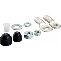
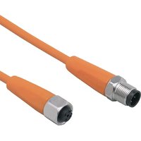
- 1 初步说明
- 1.1 符号说明
- 2 安全说明
- 3 功能和特性
- 4 功能
- 5 安装
- 5.1 安装位置
- 5.2 安装表面
- 5.3 固定
- 5.4 电缆密封件
- 6 电气连接
- 6.1 配线
- 6.2 一般配线信息
- 6.3 连接技术
- 6.4 连接附件
- 6.5 频率输入
- 6.6 反极性保护
- 6.7 输入端信号发生器的供电
- 6.8 执行器与输出端的连接
- 6.9 保险丝
- 6.10 连接类型示例
- 6.10.1 CR2040
- 6.10.2 CR2041
- 6.10.3 CR2042
- 7 操作和显示元件
- 10 段显示屏( → 9 技术资料)
- 7.1 菜单结构
- 7.2 输入/输出的状态表示(I/O LED,黄色)
- 8 设定
- 8.1 I/O 模块
- 8.1.1 显示模式
- 8.1.2 参数设定
- 8.1.3 参数列表
- 8.2 控制器
- 8.2.1 编程
- 8.3 所需文档
- 8.4 所需硬件
- 9 技术资料
- 9.1 CR2040
- 9.2 CR2041
- 9.3 CR2042
- 11 认证/标准
- 12 APPENDIX
- 12.1 EMCY OBJECT
- 12.2 OBJECT DIRECTORY CR204X
- 12.2.1 DEVICE-SPECIFIC CR2040
- 12.2.2 DEVICE-SPECIFIC CR2041
- 12.2.3 DEVICE-SPECIFIC CR2042
- 12.3 SDOS ERROR MESSAGES
- 12.3.1 CR2040
- 12.3.2 CR2041
- 12.3.3 CR2042
品牌 : IFM
型号 : CR2041
类别 : 工业自动化