
ST 450 L - Récepteur audio-vidéo MARANTZ - Notice d'utilisation et mode d'emploi gratuit
Retrouvez gratuitement la notice de l'appareil ST 450 L MARANTZ au format PDF.


| Type de produit | Récepteur audio-vidéo (tuner stéréo LW/MW/FM) |
| Marque | Marantz |
| Modèle | ST 450 L |
| Gammes de fréquences FM | 67,5 - 108 MHz |
| Gammes de fréquences MW | 531 - 1602 kHz |
| Gamme de fréquences LW | 150 - 370 kHz |
| Sensibilité FM (mono) | 0,9 µV (26 dB S/N) |
| Sensibilité FM (stéréo) | 20 µV (46 dB S/N) |
| Sélectivité canaux adjacents FM | 70 dB |
| Distorsion harmonique FM | 0,17 % (mono), 0,1 % (stéréo) |
| Rapport signal/bruit FM | 73 dB (mono), 63 dB (stéréo) |
| Séparation stéréo | 45 dB |
| Tension de sortie (1 kHz) | 700 mV |
| Impédance de sortie | 1,5 kΩ |
| Bornes d'antenne FM | 300 Ω (symétrique) / 75 Ω (dissymétrique) |
| Alimentation | 220 V AC, 50 Hz, 14 W |
| Dimensions (L x H x P) | 416 x 73 x 194 mm |
| Poids | 3,2 kg |
| Affichage | Numérique avec LED de niveau de signal |
| Fonctions spéciales | Circuit de coupure (muting), sélecteur de bande, indicateur LED |
| Entretien et nettoyage | Nettoyer avec un chiffon sec et doux. Ne pas utiliser de solvants. |
| Sécurité | Débrancher avant toute intervention. Pièces marquées Δ sont critiques pour la sécurité. |
| Pièces détachées | Disponibles via le service pièces Marantz. Utiliser uniquement des pièces d'origine. |
| Réparabilité | Manuel de service disponible avec schémas et liste de pièces. |
| Garantie | Faire appel à un centre agréé pour toute réparation sous garantie. |
FOIRE AUX QUESTIONS - ST 450 L MARANTZ
Questions des utilisateurs sur ST 450 L MARANTZ
0 question sur cet appareil. Repondez a celles que vous connaissez ou posez la votre.
Poser une nouvelle question sur cet appareil
Téléchargez la notice de votre Récepteur audio-vidéo au format PDF gratuitement ! Retrouvez votre notice ST 450 L - MARANTZ et reprennez votre appareil électronique en main. Sur cette page sont publiés tous les documents nécessaires à l'utilisation de votre appareil ST 450 L de la marque MARANTZ.
MODE D'EMPLOI ST 450 L MARANTZ
SERVICE MANUAL

MARANTZ DESIGN AND SERVICE
Using superior design and selected high grade components, MARANTZ Company has created the ultimate in stereo sound. Only original MARANTZ parts can insure that your MARANTZ product will continue to perform to the specifications for which it is famous.
Parts for your MARANTZ stereo are generally available within 72 hours throughout the nation via a toll-free line to our National Parts Depot in California. The sales professionals who take your call immediately refer to their own desk top computer terminal and can quickly determine the availability and price information you require. If for some reason, your order should exceed our available stock, we usually can instantly provide an alternate replacement part or current delivery information. When the order is placed and confirmed, the computer simultaneously generates "hard copy" orders at the distribution center. As hard copies come directly from the computer to the national parts depot, your requested stock is assembled and prepared for shipment and placed on the first available carrier for delivery to you.
ORDERING PARTS
Phone orders will eliminate mail delays, and we encourage the use of this method. If you order by mail, use MARANTZ parts order forms which are available from our National Parts Depot located at the following address:
SUPERSCOPE NATIONAL PARTS DEPARTMENT
20525 Nordhoff Street
Chatsworth, California 91311
Phone: 1-800-423-5108
1-213-998-9333
The following information must be supplied to eliminate delays in processing your order:
- Complete address.
- Complete part numbers.
- Complete description of parts.
- Model number for which part is required (indicate MARANT 27).
- Account number (for account customers only).
Direct consumers will be provided with the current retail privilege quotation on available parts in order to advise them of the cost of the parts and shipping.
OVERSEAS PARTS ORDERING
Parts may also be ordered from the following overseas addresses:
CANADA
Superscope Canada, Ltd.
3710 Nashua Drive
Mississauga
Ontario, Canada L4V1M
AUSTRALIA
Superscope (Australasia) Pty., Ltd.
32 Cross Street (P.O.Box 604)
Brookvale 2100 N.S.W.
Australia
JAPAN
Marantz Japan, Inc.
3622 Kamitsuruma
Sagamihara Shi
Kanagawa, Japan
EUROPE
Superscope Europe, S.A.
Avenue Leopold III, 2
7120 Peronnes-Lez-Binche
Belgium
Marantz France
Rue Louis Armand 9
92600 Asnieres
Hauts-de-Seine
France
Marantz Audio U.K. Ltd. London Road, 203 Staines Middlesex England
Superscope GmbH
Max-Planck-Strass 22
D-6072 Dreieich
West Germany
All of the above locations are fully equipped to take care of your total service needs. Because various countries have differing configuration requirements, it is necessary that you contact the service facility in your particular country. In the event that there is no service location listed for your country, please contact the nearest facility for the necessary assistance.
TABLE OF CONTENTS
SECTION
PAGE
- INTRODUCTION 1
2.P.W. BOARDS 1 - TEST EQUIPMENT REQUIRED FOR SERVICING 2
- BLOCK DIAGRAM 2
- ALIGNMENT PROCECURES 3
5.1 FM Alignment Procedures (Function switch in the "FM" position) 3
5.2 Muting Circuit Alignment 3
5.3 Multiplex Alignment Procedures (Function switch in the "FM" position). 3
5.4 AM Alignment Procedures (Function switch in the "AM" position) 3
5.5 Frequency Display Alignment Procedures 5
- VOLTAGE CONVERSION 5
- DIAGRAM AND COMPONENT LOCATIONS 6
7.1 Tuner Assembly (P100) Schematic Diagram and Component Locations 6
7.2 Frequency Indicator Assembly (PQ00), Sub Assembly (PC00) Schematic Diagram and Component Locations 8
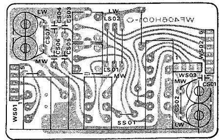
7.3 Switch Assembly (PS00) Schematic Diagram and Component Locations 9
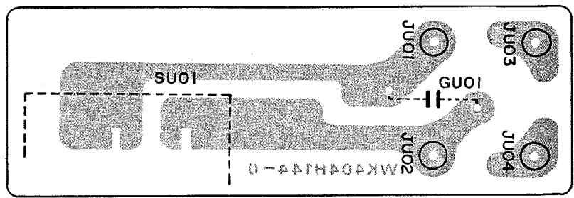
7.4 Power Switch Assembly (PU00) Schematic Diagram and Component Locations 9
7.5 LED Indicator Assembly (PX00) Schematic Diagram and Component Locations 9
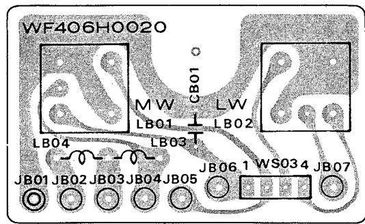
7.6 Ant. Coil Assembly (PB00) Schematic Diagram and Component Locations 9
- EXPLODED VIEW AND PARTS LIST 10
- ELECTRICAL PARTS LIST 16
- TECHNICAL SPECIFICATIONS 21
- SCHEMATIC DIAGRAMS 22

MODEL ST450L LW/MW/FM STEREOPHONIC TUNER

1. INTRODUCTION
This service manual was prepared for use by Authorized Warranty Stations and contains service information for Marantz Model ST-450L LW/MW/FM Stereophonic Tuner.
Servicing information and voltage data included in this manual are intended for use by the knowledgeable and experienced technician only. All instructions should be read carefully. No attempt should be made to proceed without a good understanding of the operations in the Tuner.
The parts list furnishes information by which replacement parts may be ordered from the Marantz Company. A simple description is included for parts which can usually be obtained through local suppliers.
2. P.W. BOARDS
As can be seen from the circuit diagram, the chassis of Model ST450L consists of the following units. Each unit mounted on a printed circuit board is described within the square enclosed by a bold dotted line on the circuit diagram.
- Tuner . . . . . . . . . . . . . . . . . . . . . . . . . . . . . . . . . . . . . . . . . . . . . . . . . . . . . . . . . . . . . . . . . . . . . . . . . . . . . . . . . . . . . . . . . . . .
- P.W. Board P100
- Frequency Indicator . . . mounted on P.W. Board P000
- Switch.... . mounted on P.W. Board PS00
- Power Switch . . . . . . . mounted on P.W. Board PU00
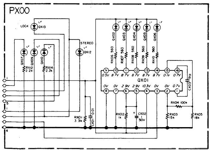
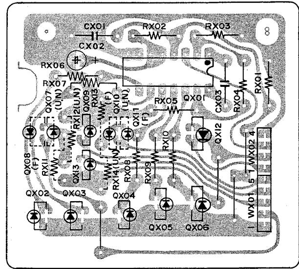
- LED Indicator . . . . . . mounted on P.W. Board PX00
- ANT Coil . . . . . . . . . . . . . . . . . . . . . . . . . . . . . . . . . . . . . . . . . . . . . . . . . . . . . . . . . . . . . . . . . . . . . . . . . . . . . . . . . . . . . . . . . . . . . . . . P.W. Board PBO0
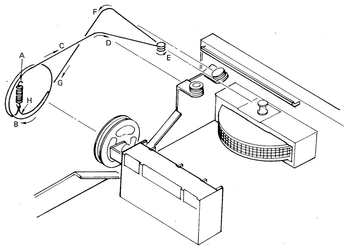
Figure 1. Dial Stringing
3. TEST EQUIPMENT REQUIRED FOR SERVICING
This table lists the test equipment required for servicing the Model ST450L Tuner.
| Item | Manufacturer and Model No. | Use |
| AM Signal Generator | Signal source for AM Alignment | |
| Test Loop | Use with AM Signal Generator | |
| FM Signal Generator MPX Signal Generator | Sound Technology Model 1000A | Signal source for FM alignment Stereo separation alignment and trouble shooting |
| Distortion Analyzer Audio Oscillator AC VTVM | Sound Technology Model 1700A | Distortion measurements Sinewave and squarewave signal source Voltage measurements (AC) |
| Oscilloscope | Tektronix Model T932 Philips Model 3232 | Waveform analysis and trouble shooting |
| Frequency Counter | MPX Oscillator adjustment (VCO) Frequency display alignment | |
| Circuit Tester | Trouble shooting | |
| DC VTVM | Fluke Model 8000 “Digital” Simpson Model 313, Triplet Model 801 | Voltage measurements (DC) |
| AC Wattmeter | Simpson Model 1379 | Monitors primary power to tuner |
| Line Voltmeter | Simpson Model 1359 | Monitors potential of primary power to tuner |
| Variable Autotransformer | Superior Electronic Co., Powerstat Model 116B-10A | Adjusts level of primary power to tuner |
4. BLOCK DIAGRAM
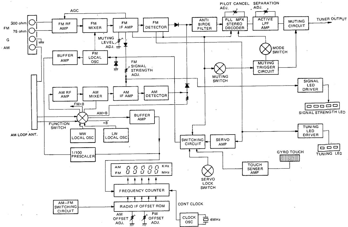
5. ALIGNMENT PROCEDURES
A dummy resistor of 47 k-ohms must be connected across the tuner output terminals before alignment.
5.1 FM Alignment Procedures (Function switch in the "FM" position)
FM RF Alignment
| Step | Signal Source Connection | Signal Frequency | Indicator Connection | Set the Digital Readout Frequency | Adjust: |
| 1 | RF generator to FM antenna terminals through matching network (300 ohms, balanced) (Maintain RF level below limit.) | 87.4 MHz | VTVM to L or R channel output (W002) | Tuning capacitor minimum closed. | L107 for maximum output. |
| 2 | 108.2 MHz | Tuning capacitor maximum open. | C116 for maximum output. | ||
| 3 | 90 MHz | 90 MHz | L101, L103, L104 for maximum output. | ||
| 4 | 106 MHz | 106 MHz | ANT, RF, TRIM, CAP, for maximum output. | ||
| 5 | Repeat steps 1 to 4. | ||||
| 6 | Check overall response curve and repeat above steps as necessary to obtain maximum sensitivity. | ||||
| 7 | No connection | No signal | “0” center meter or DC current meter in 100μA range between J201 and J202 | L201 primary core so that the meter indicates its center or may read “0”. | |
| 8 | RF generator 1mV (or 300μV, only Step 10) output to FM antenna terminals through matching network. (300 ohms, balanced) | 98 MHz | Distortion meter to L or R channel output (W002) | 98 MHz | L201 Secondary core (BLK) for minimum distortion. |
| 9 | |||||
| 10 | 98 MHz | 98 MHz | R224 so that signal strength Led may light 5 points. | ||
5.2 Muting Circuit Alignment
| Step | Signal Source Connection | Signal Frequency | Indicator Connection | Set the Digital Readout Frequency | Adjust: |
| 1 | RF generator 12.5μV output to FM antenna terminals through matching network (300 ohms, balanced) | 98 MHz | VTVM to R or L channel output (W002) | 98 MHz | R220 for 12.5μV threshold level. (During this adjustment turn the mating pushswitch “ON”). |
5.3 Multiplex Alignment Procedures (Function switch in the "FM" position)
| Step | Signal Source Connection | Signal Frequency | Indicator Connection | Set the Digital Readout Frequency | Adjust: |
| 1 | RF generator to FM antenna terminals through matching network (300 ohms, balanced), with 1mV FM stereo simulator RF level and 100% modulation (pilot 9%) | No Modulation | Frequency counter to J301 | 98 MHz | R303 so that Frequency counter may precisely read 76 kHz |
| 2 | Stereo, left (1,000 Hz) | VTVM to right channel output (W002, red) | R319 for maximum output and same separation in both channels. | ||
| 3 | Stereo, right (1,000 Hz) | VTVM to left channel output (W002, white) | |||
| 4 | Repeat steps 2 and 3. | ||||
5.4 AM Alignment Procedures
- MW IF Alignment (Function switch in the "MW" position)
| Step | Signal Source Connection | Signal Frequency | Indicator Connection | Set Dial Pointer to: | Adjust: |
| 1 | Sweep generator to OSC Variable Cap. | 455 kHz marker | Oscilloscope to JA06 | Quiet point on band | LA02 & LA03 for maximu m and symmetric response. |

- MW RF Alignment (Function switch in the "MW" position)
| Step | Signal Source | Signal Frequency | Indicator Connection | Set the Digital Readout Frequency | Adjust: |
| 1 | Apply the signal to the AM Loop antenna from the RF generator, using the test loop, as per the Figure 2. | 525 kHz | VTVM to L or R channel output (W002) | Tuning capacitor minimum closed. | LS01 for maximum output. |
| 2 | 1,630 kHz | Tuning capacitor maximum open. | CS07-1 for maximum output. | ||
| 3 | 600 kHz | 600 kHz | LB01 for maximum output. | ||
| 4 | 1,400 kHz | 1,400 kHz | CS02-1 for maximum maximum output. | ||
| 5 | Repeat steps 1 to 4 as necessary to obtain maximum sensitivity. | ||||
- LW RF Alignment (Function switch in the "LW" position)
| Step | Signal Source | Signal Frequency | Indicator Connection | Set the Digital Readout Frequency | Adjust: |
| 1 | Apply the signal to the AM Loop antenna from the RF generator, using the test loop, as per the Figure 2. | 145 kHz | VTVM to L or R channel output (W002) | Tuning capacitor minimum closed. | LS02 for maximum output. |
| 2 | 380 kHz | Tuning capacitor maximum open. | CS07--1 for maximum maximum output. | ||
| 3 | 170 kHz | 170 kHz | LB02 for maximum output. | ||
| 4 | 350 kHz | 350 kHz | CS02-2 for maximum maximum output. | ||
| 5 | Repeat steps 1 to 4 as necessary to obtain maximum sensitivity. | ||||
- IF TRAP Alignment (Function switch in the "LW" position)
| Step | Signal Source Connection | Signal Frequency | Indicator Connection | Set Tuning | Adjust: |
| 1 | Apply the signal to the AM Loop antenna from the RF generator, using the test loop, as per the Figure 2. | 455 kHz | VTVM to L or R channel output (W002) | 350 kHz | LA04 for minimum output. |
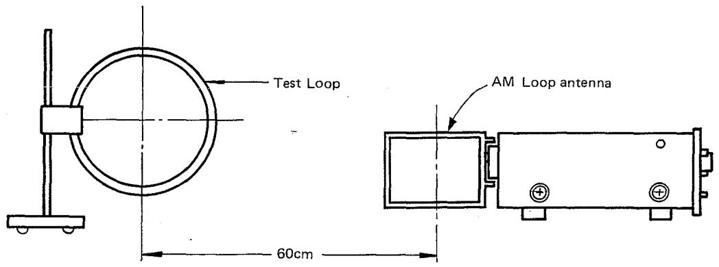
Figure 2. Application of AM Signal
5.5 Frequency Display Alignment Procedures
1. FM Alignment
| Step | Signal Source Connection | Signal Frequency | Indicator Connection | Set Tuning | Adjust: | |
| 1 | RF generator 1mV output to FM antenna terminals through matching network. (300 ohm, balanced) | 98.025 MHz | “O” center meter or DC current meter in 100μA range between J201 and J202 | 98.025 MHz | Meter indicates its center or may read “O” | R002 so that the flicker of 98.00/98.05 MHz can be occurred on the Digital Readout Freq. display. |
2. MW Alignment
| 1 | Apply the signal to the AM Loop Antenna from the RF generator using the test loop. As per the Figure 2.(with 5mV/m) (modulation 5kHz 30%) | 600.5 kHz | VTVM to R or L channel output (W002) | 600.5 kHz Tune precisely to dip point of 5 kHz output | RQ01 so that the flicker of 600/601 kHz can be occurred on the Digital Readout Freq. display. |
6. VOLTAGE CONVERSION
EUROPEAN MODEL ONLY
To convert the unit to a different power source voltage, change the position as illustrated in the drawing below.
CAUTION
DISCONNECT POWER SUPPLY CORD FROM AC OUTLET BEFORE CONVERTING VOLTAGE. DO NOT DISASSEMBLE THE VOLTAGE SELECTOR ABSOLUTELY.
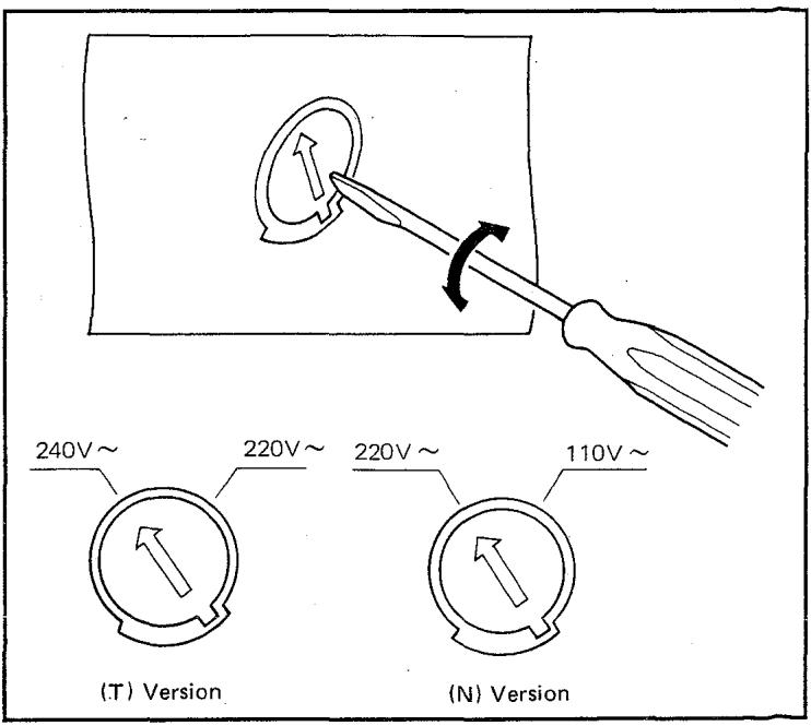
Voltage Conversion Chart
NOTE ON SAFETY:
THE PARTS MARKED WITH ARE IMPORTANT PARTS ON THE SAFETY.
PLEASE USE THE PARTS HAVING THE DESIGNATED PARTS NUMBERS WITHOUT FAIL.
FTZ REGULATION
Instruction for the use in the range other than specified in FTZ codes.
Achtung für die Leute, die in dem Gebiet wohnen, wo die FTZ-Bestimmungen vorherrschend sind.
Sollte des Gerät auch für Frenzen auszerhalb des in den FTZ-Bestimmungen angegebenen Bereiches empfangebereit sein, bitten wir, den Bereich durch Nachstellen des Kernes in der Oszillatorspule (in der Abbildung mit "FTZ" gekennzeichnet) so zu korrigieren, dass er den Bestimmungen entspricht.

7. DIAGRAM AND COMPONENT LOCATIONS
7.1 Tuner Assembly (P100) Schematic Diagram and Component Locations
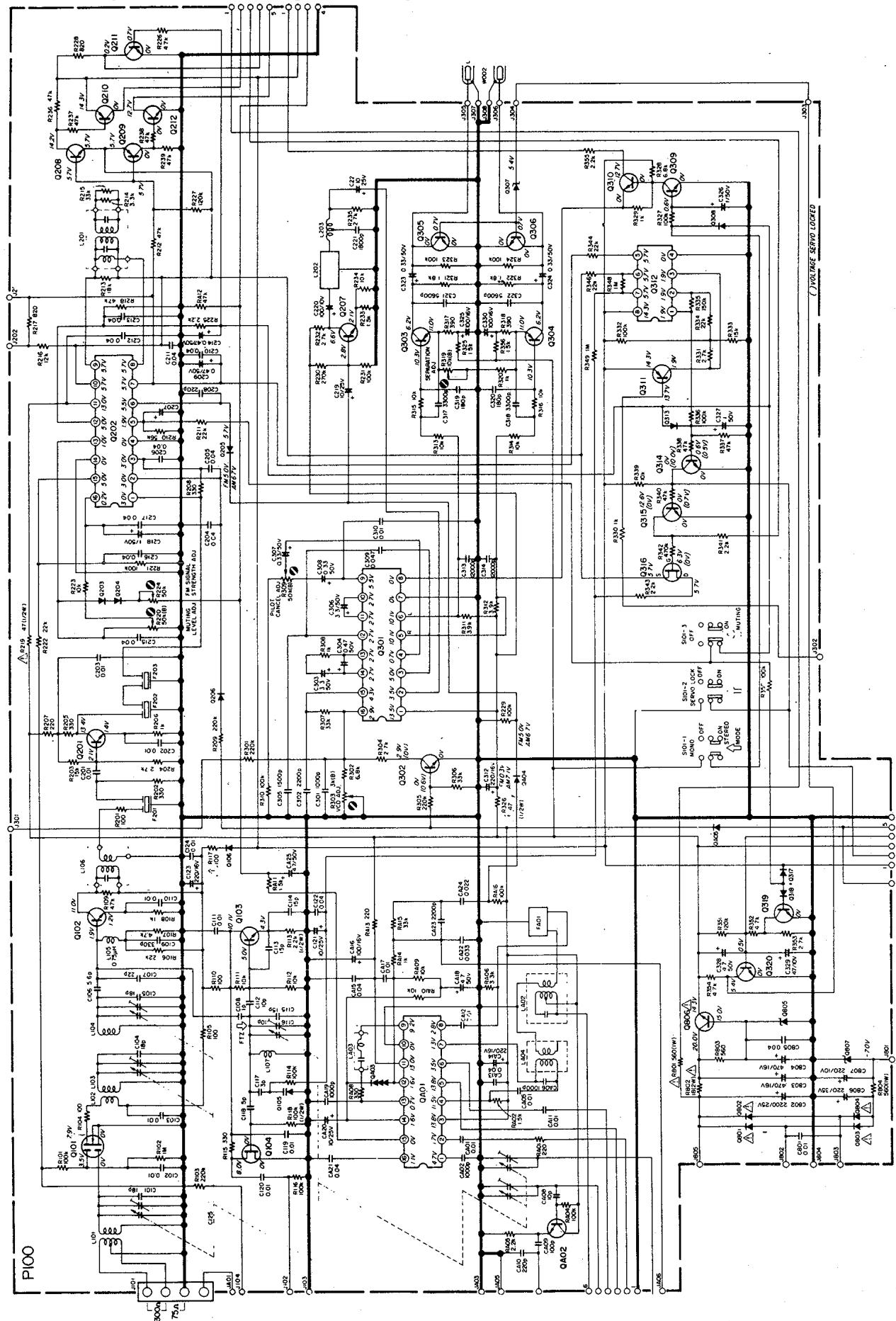
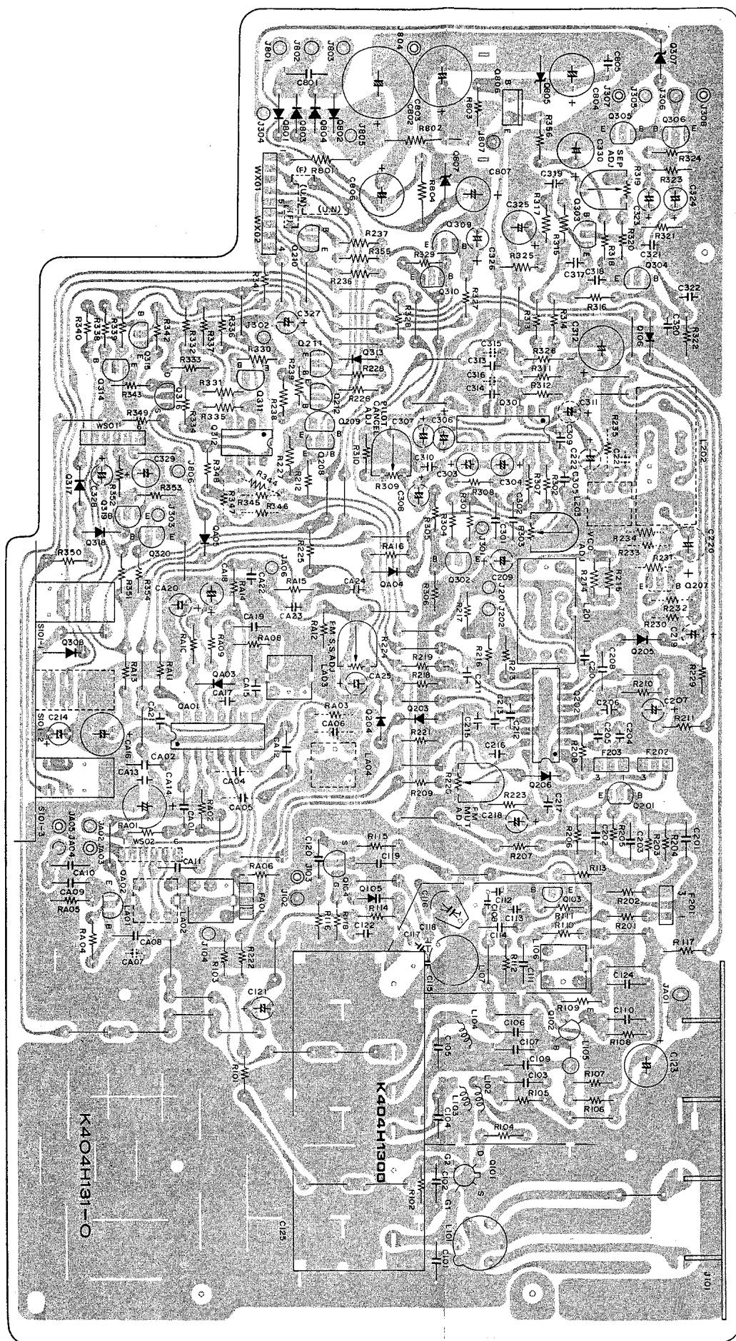

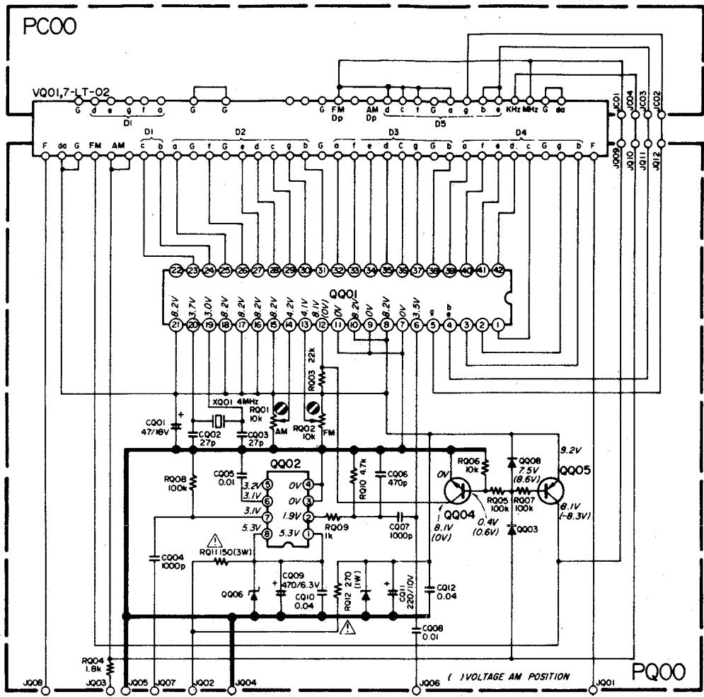
7.2 Frequency Indicator Assembly (PQ00), Sub Assembly (PC00) Schematic Diagram and Component Locations
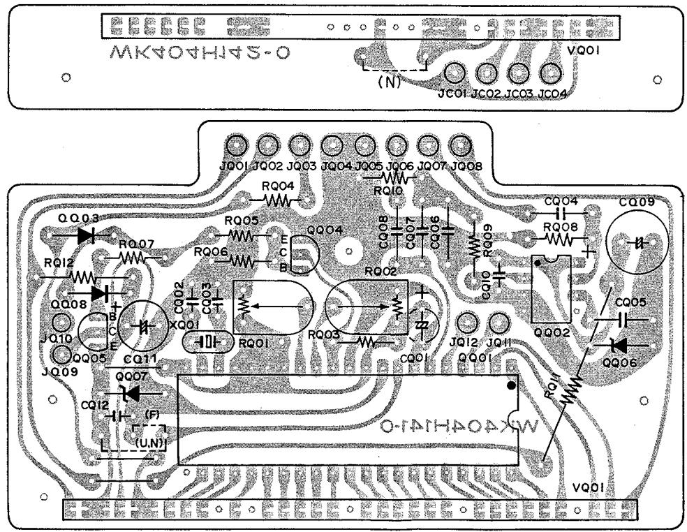

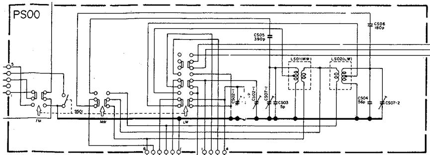
7.3 Switch Assembly (PS00) Schematic Diagram and Component Locations
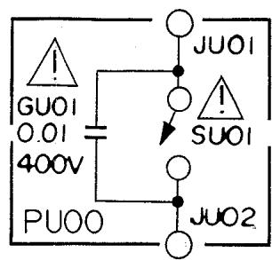
7.4 Power Switch Assembly (PU00) Schematic Diagram and Component Locations
7.5 LED Indicator Assembly (PX00) Schematic Diagram and Component Locations
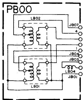
7.6 Ant. Coil Assembly (PB00) Schematic Diagram and Component Locations
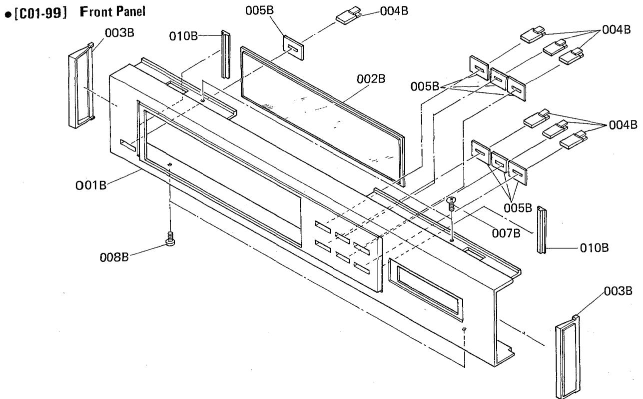
8. EXPLODED VIEW AND PARTS LIST
| REF. DESIG. | Q'TY | PART NO. | DESCRIPTION |
| N | |||
| A | 1 | 406H063400 | Front Panel Assembly |
| 001B | 1 | 406H063010 | Escutcheon |
| 002B | 1 | 404H158010 | Window |
| 003B | 2 | 403H067010 | Cap |
| 004B | 7 | 208H154020 | Knob |
| 005B | 7 | 208H259010 | Bushing |
| 010B | 2 | 403H063020 | Escutcheon |
| REF. DESIGN. | Q'TY N | PART NO. | DESCRIPTION |
| 007B | 2 | 51280308B0 | B.H.Tapped Screw B3x8 |
| 008B | 2 | 51280308B0 | B.H.Tapped Screw B3x8 |
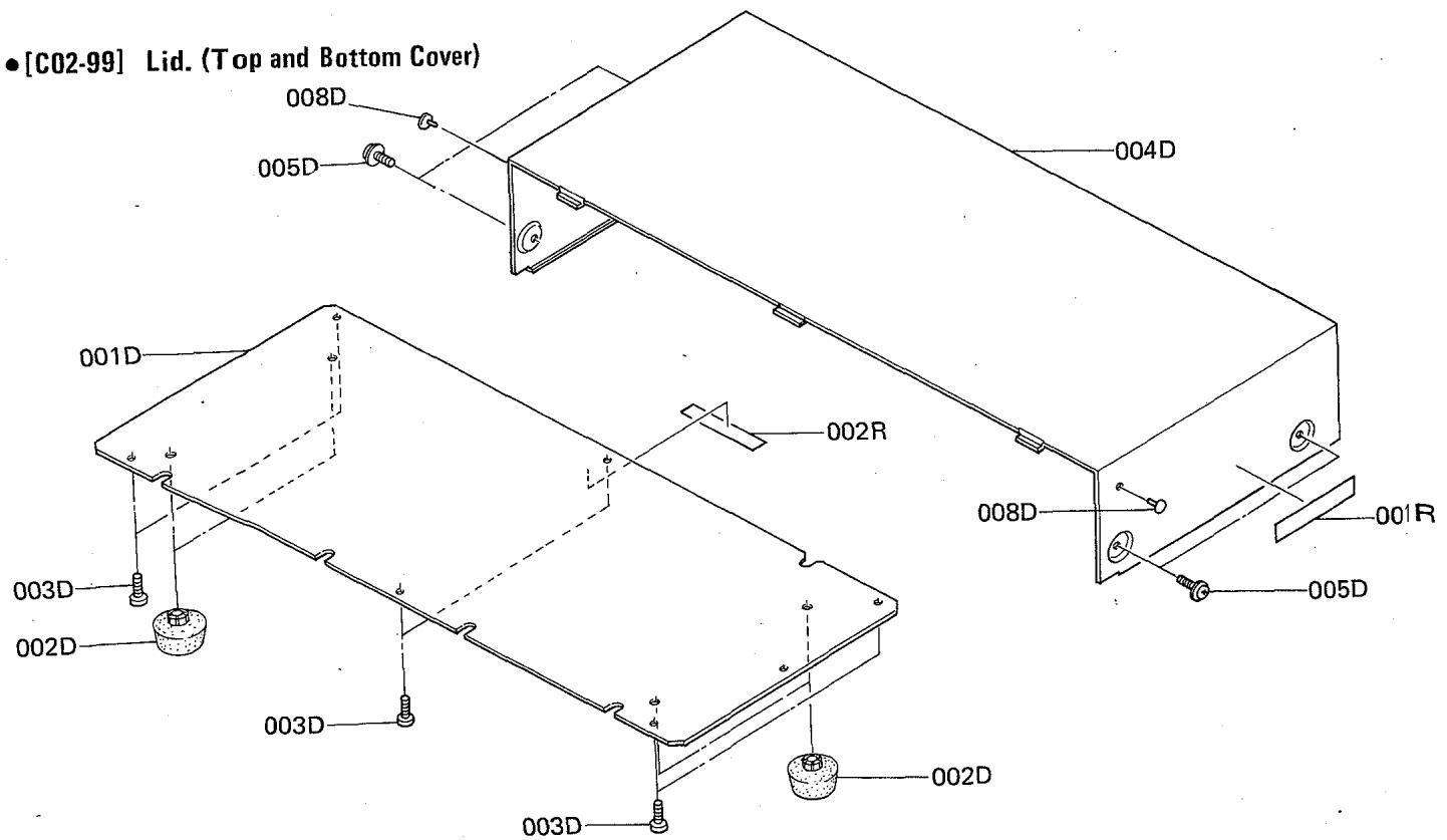
| REF. DESIGN. | Q'TY | PART NO. | DESCRIPTION |
| N | |||
| 001D | 1 | 403H257020 | Lid. Bottom Cover |
| 002D | 4 | 403H057010 | Leg |
| 003D | 6 | 51280308B0 | B.H.Tapped Screw B3x8 |
| 004D | 1 | 403H257010 | Lid. Top Cover |
| 005D | 4 | 51260408Z0 | B.T. Screw B4x8 |
| 008D | 2 | 2991259010 | Bushing |
| REF. DESIGN. | Q'TY N | PART NO. | DESCRIPTION |
| 001R 002R | 1 1 | 29328610102578861010 | Label Label |
[C03-99] Rear Panel
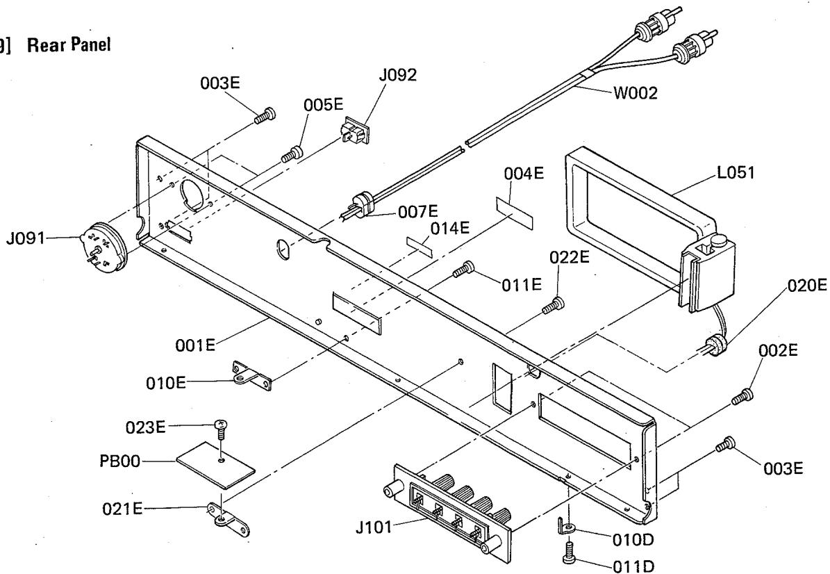
| REF. DESIG. | Q'TY | PART NO. | DESCRIPTION |
| N | |||
| 010D | 1 | 404H123010 | Contactor |
| 011D | 1 | 51280308B0 | B.H.Tapped Screw B3x8 |
| 001E | 1 | 406H160210 | Bracket, Rear Panel |
| 002E | 2 | 51280308U0 | B.H.Tapped Screw B3x8 |
| 003E | 4 | 51280308U0 | B.H.Tapped Screw B3x8 |
| 004E | 1 | 2112265010 | Indicator |
| 005E | 2 | 51280310U0 | B.H.Tapped Screw B3x10 |
| 007E | 1 | 1455259090 | Bushing |
| 010E | 1 | 404H160030 | Bracket |
| 011E | 1 | 51280308U0 | B.H.Tapped Screw B3x8 |
| 014E | 1 | 4581861010 | Label |
| 020E | 1 | 1455259010 | AM Loop ANT Read |
| 021E | 1 | 404H160030 | Bracket |
| 022E | 1 | 51280308U0 | B.H.Tapped Screw B3x8 |
| 023E | 1 | 51280308U0 | B.H.Tapped Screw B3x8 |
| REF. DESIG. | Q'TY | PART NO. | DESCRIPTION |
| N | |||
| △ J091 | 1 | BY05060040 | Voltage Selector |
| △ J092 | -1 | YP04000580 | Plug, AC Inlet |
| J101 | 1 | YT01040220 | Ant. Terminal |
| L051 | 1 | LA00015010 | AM Loop Ant. |
| W002 | 1 | YB01000300 | Connective Cord |
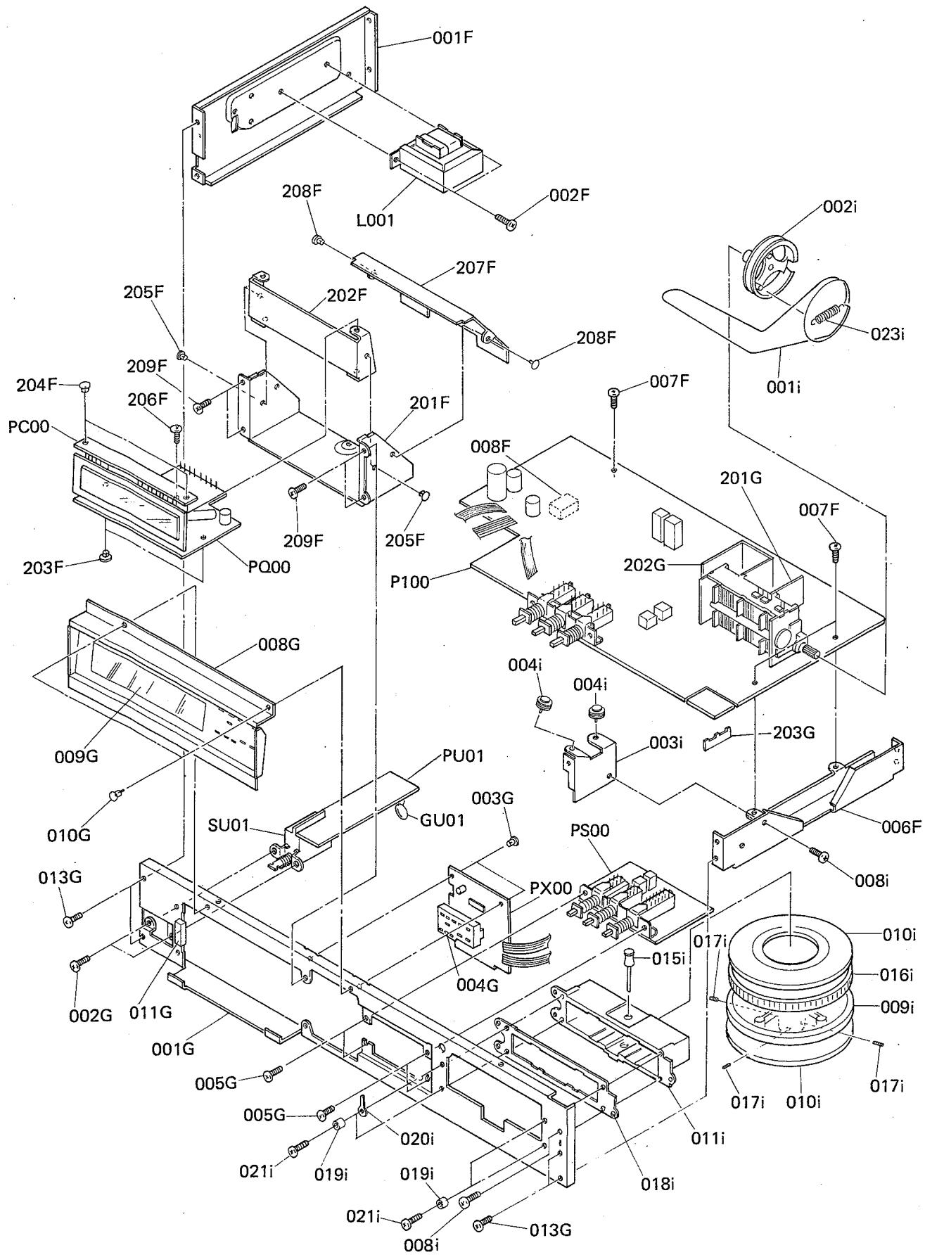
| REF. DESIG. | Q'TY | PART NO. | DESCRIPTION |
| N | |||
| 001F | 1 | 404H126010 | Stay |
| 002F | 2 | 61280406B0 | B.H.Tapped Screw B4x6 |
| 006F | 1 | 404H126020 | Stay |
| 007F | 3 | 51260308B0 | B.T. Screw B3x8 |
| 008F | 1 | 404H056010 | Buffer |
| 201F | 1 | 404H109010 | Shield |
| 202F | 1 | 404H109030 | Shield |
| 203F | 2 | 2912259020 | Bushing |
| 204F | 2 | 2912259020 | Bushing |
| 205F | 2 | 2912259020 | Bushing |
| 206F | 1 | 51280308B0 | B.H.Tapped Screw B3x8 |
| 207F | 1 | 404H109020 | Shield |
| 208F | 2 | 2912259020 | Bushing |
| 209F | 4 | 51280308B0 | B.H.Tapped Screw B3x8 |
| 001G | 1 | 404H160010 | Bracket, Front Chassis |
| 002G | 2 | 51100306A9 | B.H.M. Screw B3x6 |
| 003G | 2 | 2276005060 | Clamper |
| 004G | 1 | 404H259010 | Bushing |
| 005G | 4 | 51100306A9 | B.H.M. Screw B3x6 |
| 008G | 1 | 404H302010 | Dial |
| 009G | 1 | 2137158020 | Window |
| 011G | 1 | 3940118010 | Bushing |
| 010G | 2 | 2912259020 | Bushing |
| 013G | 4 | 51280308B0 | B.H.Tapped Screw B3x8 |
| 201G | 1 | 2259109040 | Shield |
| 202G | 1 | 2259109050 | Shield |
| 203G | 1 | 2259109060 | Shield |
| REF. DESIG. | Q'TY | PART NO. | DESCRIPTION |
| N | |||
| 001j | 60 | 72040805A0 | String |
| 002i | 1 | 2116159010 | Drum |
| 003i | 1 | 404H160020 | Bracket |
| 004j | 2 | 2276262500 | Pulley |
| 008i | 2 | 51280308B0 | B.H.Tapped Screw B3x8 |
| 009i | 1 | 2219273010 | Flywheel |
| 010i | 2 | 2219063230 | Escutcheon |
| 011i | 1 | 2112104500 | Retainer |
| 015i | 1 | 2219112010 | Shaft |
| 016i | 1 | 2286353010 | Ring |
| 017i | 3 | 51690306Q9 | Socket Screw |
| 018i | 1 | 2286120010 | Insulator |
| 019i | 4 | 2219259030 | Bushing |
| 020i | 1 | 62030049W0 | Lug |
| 021i | 4 | 51280310B0 | B.H.Tapped Screw B3x10 |
| 023i | 1 | 2112115020 | Spring |
| △L001 | 1 | TS14808330 | Power Transformer |
| △GU01 | 1 | DK18103840 | Ceramic 0.01μF |
| △SU01 | 1 | SP01010390 | Push Switch |
| REF. DESIG. | Q'TY | PART NO. | DESCRIPTION |
| N | |||
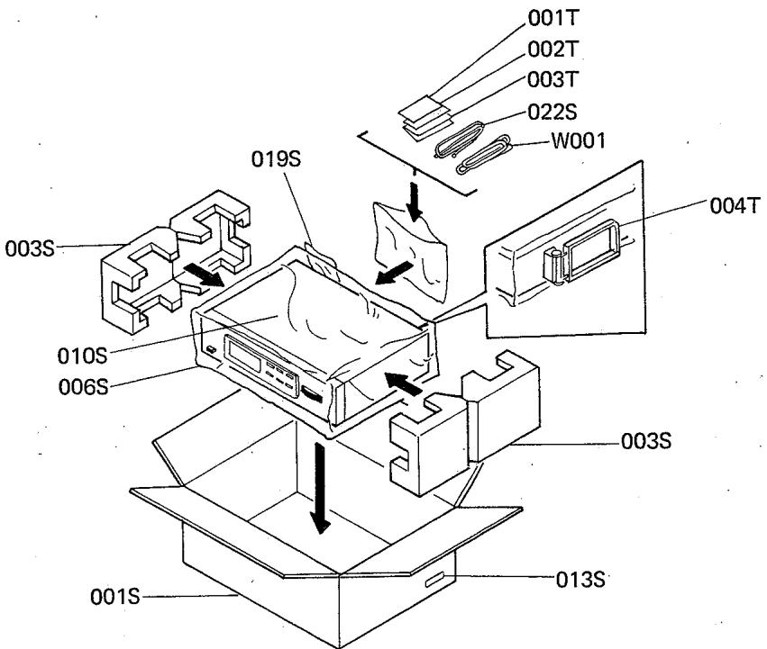
| 001S | 1 | 406H801010 | Packing Case |
| 003S | 2 | 001H809010 | Cushion |
| 006S | 1 | 9090909040 | Polyethylene Sheet |
| 010S | 1 | 2918107360 | Sheet |
| 013S | 2 | 9526019060 | Serial No. Card |
| 015S | 1 | 2819056020 | Buffer |
| 019S | 1 | 2731821010 | Silicagel |
| 022S | 1 | ZA02000070 | Ext. Antenna |
| REF. DESIG. | Q'TY | PART NO. | DESCRIPTION |
| N | |||
| 001T | 1 | 403H851310 | Instructions |
| 002T | 1 | 406H851320 | Instructions |
| 003T | 1 | 406H856010 | Circuit Diagram |
| 004T | 1 | 2864804010 | Sleeve |
| △W001 | 1 | ZC01805010 | A.C. Power Cord |
- ELECTRICAL PARTS LIST
| REF. DESIG. | Q'TY | PART NO. | DESCRIPTION |
| N | |||
| P100 | 1 | WK404H1310 | P100-TUNER CIRCUIT BOARD |
| 1 | ZZ404H7310 | P.W. Board, Tuner | |
| P.W. Board Assembly | |||
| C101 | 1 | DA15180010 | P100-CAPACITORS |
| C102 | 1 | DA17103010 | Ceramic 18pF ±5% |
| C103 | 1 | DA17103010 | Ceramic 0.01μF ±20% |
| C104 | 1 | DA15180010 | Ceramic 0.01μF ±20% |
| C105 | 1 | DA15180010 | Ceramic 18pF ±5% |
| C106 | 1 | DA16056010 | Ceramic 5.6pF ±10% |
| C107 | 1 | DA15220010 | Ceramic 22pF ±5% |
| C108 | 1 | DD10010300 | Ceramic 1pF ±0.25pF |
| C109 | 1 | DA16331010 | Ceramic 330pF ±10% |
| C110 | 1 | DA17103010 | Ceramic 0.01μF ±20% |
| C111 | 1 | DA17103010 | Ceramic 0.01μF ±20% |
| C112 | 1 | DD11100300 | Ceramic 10pF ±0.5pF |
| C113 | 1 | DD15150300 | Ceramic 15pF ±5% |
| C114 | 1 | DA15150020 | Ceramic 15pF ±5% |
| C115 | 1 | DD15150340 | Ceramic 15pF ±5% |
| C116 | 1 | CT11000010 | Trimming 10pF |
| C117 | 1 | DD10030300 | Ceramic 3pF ±0.25pF |
| C118 | 1 | DD10050300 | Ceramic 5pF ±0.25pF |
| C119 | 1 | DA17103010 | Ceramic 0.01μF ±20% |
| C120 | 1 | DA17103010 | Ceramic 0.01μF ±20% |
| C121 | 1 | EA10602530 | Elect 10μF 25V |
| C122 | 1 | DK18403320 | Ceramic 0.04μF |
| C123 | 1 | EA22701630 | Elect 220μF 16V |
| C124 | 1 | DA17103010 | Ceramic 0.01μF ±20% |
| C125 | 1 | CA42300010 | Variable |
| C201 | 1 | DA17103010 | Ceramic 0.01μF ±20% |
| C202 | 1 | DA17103010 | Ceramic 0.01μF ±20% |
| C203 | 1 | DA17103010 | Ceramic 0.01μF ±20% |
| C204 | 1 | DK18403320 | Ceramic 0.04μF |
| C205 | 1 | DK18403320 | Ceramic 0.04μF |
| C206 | 1 | DK18403320 | Ceramic 0.04μF |
| C207 | 1 | EA47505030 | Elect 4.7μF 50V |
| C208 | 1 | DA16221010 | Ceramic 220pF ±10% |
| C209 | 1 | EA47405030 | Elect 0.47μF 50V |
| C210 | 1 | DK18403320 | Ceramic 0.04μF |
| C211 | 1 | DK18403320 | Ceramic 0.04μF |
| C212 | 1 | DK18403320 | Ceramic 0.04μF |
| C213 | 1 | DK18403320 | Ceramic 0.04μF |
| C214 | 1 | EA47405030 | Elect 0.47μF 50V |
| C215 | 1 | DK18403320 | Ceramic 0.04μF |
| C216 | 1 | DK18403320 | Ceramic 0.04μF |
| C217 | 1 | DK18403320 | Ceramic 0.04μF |
| C218 | 1 | EA10505030 | Elect 1μF 50V |
| C219 | 1 | EA10602530 | Elect 10μF 25V |
| C220 | 1 | EA10701030 | Elect 100μF 10V |
| C221 | 1 | DF15182300 | Film 1800pF ±5% |
| C222 | 1 | EA10602530 | Elect 10μF 25V |
| C301 | 1 | DF55102090 | Film 1000pF ±5% |
| C302 | 1 | DF15222300 | Film 2200pF ±5% |
| C303 | 1 | EA33505030 | Elect 3.3μF 50V |
| REF. DESIG. | Q'TY | PART NO. | DESCRIPTION | ||
| N | |||||
| C304 | 1 | EA47405030 | Elect | 0.47μF | 50V |
| C305 | 1 | DF15152300 | Film | 1500pF ±5% | |
| C306 | 1 | EA33505030 | Elect | 0.33μF | 50V |
| C307 | 1 | EA33405030 | Elect | 0.33μF | 50V |
| C308 | 1 | EA33405030 | Elect | 0.33μF | 50V |
| C309 | 1 | DF15473300 | Film | 0.047μF ±5% | |
| C310 | 1 | DF15103300 | Film | 0.01μF ±5% | |
| C312 | 1 | EA22701630 | Elect | 220μF | 16V |
| C313 | 1 | DF15123300 | Film | 0.023μF ±5% | |
| C314 | 1 | DF15123300 | Film | 0.023μF ±5% | |
| C317 | 1 | DF15332300 | Film | 3300pF ±5% | |
| C318 | 1 | DF15332300 | Film | 3300pF ±5% | |
| C319 | 1 | DD15181370 | Ceramic | 180pF ±5% | |
| C320 | 1 | DD15181370 | Ceramic | 180pF ±5% | |
| C321 | 1 | DF15562300 | Film | 5600pF ±5% | |
| C322 | 1 | DF15562300 | Film | 5600pF ±5% | |
| C323 | 1 | EA33405030 | Elect | 0.33μF | 50V |
| C324 | 1 | EA33405030 | Elect | 0.33μF | 50V |
| C325 | 1 | EA10701630 | Elect | 100μF | 16V |
| C326 | 1 | EA10505030 | Elect | 1μF | 50V |
| C327 | 1 | EA10505030 | Elect | 1μF | 50V |
| C328 | 1 | EA47505030 | Elect | 4.7μF | 50V |
| C329 | 1 | EA47601030 | Elect | 47μF | 10V |
| C330 | 1 | EA10701630 | Elect | 100μF | 16V |
| C801 | 1 | DK18103560 | Ceramic | 0.01μF | |
| C802 | 1 | EA22802530 | Elect | 2200μF | 25V |
| C803 | 1 | EA47702530 | Elect | 470μF | 25V |
| C804 | 1 | EA47701630 | Elect | 470μF | 16V |
| C805 | 1 | DK18403320 | Ceramic | 0.04μF | |
| C806 | 1 | EA22703530 | Elect | 220μF | 35V |
| C807 | 1 | EA22701030 | Elect | 220μF | 10V |
| CA01 | 1 | DA17103010 | Ceramic | 0.01μF ±20% | |
| CA02 | 1 | DA17102010 | Ceramic | 1000pF ±20% | |
| CA05 | 1 | DA17103010 | Ceramic | 0.01μF ±20% | |
| CA06 | 1 | DA17102010 | Ceramic | 1000pF ±20% | |
| CA08 | 1 | DA15100020 | Ceramic | 10pF ±5% | |
| CA09 | 1 | DA15101010 | Ceramic | 100pF ±5% | |
| CA10 | 1 | DA16221010 | Ceramic | 220pF ±10% | |
| CA11 | 1 | DA17103010 | Ceramic | 0.01μF ±20% | |
| CA12 | 1 | DA17103010 | Ceramic | 0.01μF ±20% | |
| CA13 | 1 | DK18403320 | Ceramic | 0.04μF | |
| CA14 | 1 | EA22701630 | Elect | 220μF | 16V |
| CA15 | 1 | DK18403320 | Ceramic | 0.04μF | |
| CA16 | 1 | EA10701630 | Elect | 100μF | 16V |
| CA17 | 1 | DK18103320 | Ceramic | 0.01μF | |
| CA18 | 1 | EA47505030 | Elect | 4.7μF | 50V |
| CA19 | 1 | DA17102010 | Ceramic | 1000pF ±20% | |
| CA20 | 1 | EA10602530 | Elect | 10μF | 25V |
| CA21 | 1 | DK18403320 | Ceramic | 0.04μF | |
| CA22 | 1 | DK18333310 | Ceramic | 0.033μF | |
| CA23 | 1 | DF15222300 | Ceramic | 2200pF ±5% | |
| CA24 | 1 | DF15223300 | Ceramic | 0.022μF ±5% | |
| CA25 | 1 | EA47505030 | Elect | 4.7μF | 50V |
| REF. DESIG. | Q'TY | PART NO. | DESCRIPTION |
| P100-RESISTORS(All Resistors are ±5% and 1/4W) | |||
| R101 | 1 | GD05104140 | 100kΩ |
| R102 | 1 | GD05105140 | 1MΩ |
| R103 | 1 | GD05224140 | 220kΩ |
| R104 | 1 | GD05101140 | 100Ω |
| R105 | 1 | GD05101140 | 100Ω |
| R106 | 1 | GD05223140 | 22kΩ |
| R107 | 1 | GD05472140 | 4.7kΩ |
| R108 | 1 | GD05102140 | 1kΩ |
| R109 | 1 | GD05473140 | 47kΩ |
| R110 | 1 | GD05101140 | 100kΩ |
| R111 | 1 | GD05103140 | 10kΩ |
| R112 | 1 | GD05103140 | 10kΩ |
| R113 | 1 | GD05222140 | 2.2kΩ |
| R114 | 1 | GD05104140 | 100kΩ |
| R115 | 1 | GD05331140 | 330Ω |
| R116 | 1 | GD05104140 | 100kΩ |
| R117 | 1 | GG05101140 | 100Ω |
| R118 | 1 | GD05104140 | 100kΩ |
| R201 | 1 | GD05101140 | 100Ω |
| R202 | 1 | GD05331140 | 330Ω |
| R203 | 1 | GD05153140 | 1.5kΩ |
| R204 | 1 | GD05272140 | 2.7kΩ |
| R205 | 1 | GD05331140 | 330Ω |
| R206 | 1 | GD05102140 | 1kΩ |
| R207 | 1 | GD05221140 | 220Ω |
| R208 | 1 | GD05331140 | 330Ω |
| R209 | 1 | GD05224140 | 220kΩ |
| R210 | 1 | GD05563140 | 56kΩ |
| R211 | 1 | GD05223140 | 22kΩ |
| R212 | 1 | GD05473140 | 47kΩ |
| R213 | 1 | GD05183140 | 18kΩ |
| R214 | 1 | GD05332140 | 3.3kΩ |
| R215 | 1 | GD05333140 | 33kΩ |
| R216 | 1 | GD05123140 | 12kΩ |
| R217 | 1 | GD05821140 | 820Ω |
| R218 | 1 | GD05473140 | 47kΩ |
| R219 | 1 | GG05470120 | 47Ω 1/2W |
| R220 | 1 | RA05030090 | Trimming 50kΩ |
| R221 | 1 | GD05104140 | 100kΩ |
| R222 | 1 | GD05223140 | 22kΩ |
| R223 | 1 | GD05103140 | 10kΩ |
| R224 | 1 | RA05030090 | Trimming 50kΩ |
| R225 | 1 | GD05222140 | 2.2kΩ |
| R226 | 1 | GD05472140 | 4.7kΩ |
| R227 | 1 | GD05124140 | 120kΩ |
| R228 | 1 | GD05821140 | 820Ω |
| R229 | 1 | GD05104140 | 100kΩ |
| R230 | 1 | GD05274140 | 270kΩ |
| R231 | 1 | GD05104140 | 100kΩ |
| R232 | 1 | GD05272140 | 2.7kΩ |
| REF. DESIG. | Q'TY N | PART NO. | DESCRIPTION |
| R233 | 1 | GD05152140 | 1.5kΩ |
| R234 | 1 | GD05103140 | 10kΩ |
| R235 | 1 | GD05272140 | 2.7kΩ |
| R236 | 1 | GD05473140 | 47kΩ |
| R237 | 1 | GD05473140 | 47kΩ |
| R238 | 1 | GD05473140 | 47kΩ |
| R239 | 1 | GD05473140 | 47kΩ |
| R301 | 1 | GD05224140 | 220kΩ |
| R302 | 1 | GD05682140 | 6.8kΩ |
| R303 | 1 | RA03020030 | Trimming 3kΩ |
| R304 | 1 | GD05272140 | 2.7kΩ |
| R305 | 1 | GD05224140 | 220kΩ |
| R306 | 1 | GD05333140 | 33kΩ |
| R307 | 1 | GD05333140 | 33kΩ |
| R308 | 1 | GD05102140 | 1kΩ |
| R309 | 1 | RA05030090 | Trimming 50kΩ |
| R310 | 1 | GD05104140 | 100kΩ |
| R311 | 1 | GD05392140 | 3.9kΩ |
| R312 | 1 | GD05892140 | 3.9kΩ |
| R313 | 1 | GD05103140 | 10kΩ |
| R314 | 1 | GD05103140 | 10kΩ |
| R315 | 1 | GD05103140 | 10kΩ |
| R316 | 1 | GD05103140 | 10kΩ |
| R317 | 1 | GD05391140 | 390Ω |
| R318 | 1 | GD05391140 | 390Ω |
| R319 | 1 | RA01030260 | Trimming 10kΩ |
| R320 | 1 | GD05102140 | 1kΩ |
| R321 | 1 | GD05182140 | 1.8kΩ |
| R322 | 1 | GD05182140 | 1.8kΩ |
| R323 | 1 | GD05104140 | 100kΩ |
| R324 | 1 | GD05104140 | 100kΩ |
| R325 | 1 | GD05152140 | 1.5kΩ |
| R326 | 1 | GG05470120 | 47Ω 1/2W |
| R327 | 1 | GD05104140 | 100kΩ |
| R328 | 1 | GD05682140 | 6.8kΩ |
| R329 | 1 | GD05102140 | 1kΩ |
| R330 | 1 | GD05102140 | 1kΩ |
| R331 | 1 | GD05272140 | 2.7kΩ |
| R332 | 1 | GD05104140 | 100kΩ |
| R333 | 1 | GD05153140 | 15kΩ |
| R334 | 1 | GD05223140 | 22kΩ |
| R335 | 1 | GD05154140 | 150kΩ |
| R336 | 1 | GD05104140 | 100kΩ |
| R337 | 1 | GD05473140 | 47kΩ |
| R338 | 1 | GD05473140 | 47kΩ |
| R339 | 1 | GD05103140 | 10kΩ |
| R340 | 1 | GD05473140 | 47kΩ |
| R341 | 1 | GD05222140 | 2.2kΩ |
| R342 | 1 | GD05474140 | 470kΩ |
| R343 | 1 | GD05222140 | 2.2kΩ |
| R344 | 1 | GD05223140 | 22kΩ |
| R346 | 1 | GD05223140 | 22kΩ |
| R348 | 1 | GD05105140 | 1MΩ |
| R349 | 1 | GD05105140 | 1MΩ |
| R350 | 1 | GD05104140 | 100kΩ |
| R351 | 1 | GD05124140 | 120kΩ |
| R352 | 1 | GD05472140 | 4.7kΩ |
| R353 | 1 | GD05272140 | 2.7kΩ |
| R354 | 1 | GD05472140 | 4.7kΩ |
| R355 | 1 | GD05222140 | 2.2kΩ |
| REF. DESIG. | Q'TY | PART NO. | DESCRIPTION |
| N | |||
| R356 | 1 | GD05152140 | 1.5kΩ |
| ΔR801 | 1 | GA05561010 | 560Ω 1W |
| ΔR802 | 1 | GJ05180020 | 18Ω 2W |
| R803 | 1 | GG05561140 | 560Ω |
| R804 | 1 | GA05561010 | 560Ω 1W |
| RA01 | 1 | GD05221140 | 220Ω |
| RA02 | 1 | GD05152140 | 1.5kΩ |
| RA04 | 1 | GD05104140 | 100kΩ |
| RA05 | 1 | GD05222140 | 2.2kΩ |
| RA06 | 1 | GD05332140 | 3.3kΩ |
| RA08 | 1 | GD05331140 | 330Ω |
| RA09 | 1 | GD05103140 | 10kΩ |
| RA10 | 1 | GD05103140 | 10kΩ |
| RA11 | 1 | GD05152140 | 1.5kΩ |
| RA12 | 1 | GD05473140 | 47kΩ |
| RA13 | 1 | GD05221140 | 220Ω |
| RA14 | 1 | GD05102140 | 1kΩ |
| RA15 | 1 | GD05333140 | 33kΩ |
| RA16 | 1 | GD05104140 | 100kΩ |
| P100-SEMICONDUCTORS | |||
| Q101 | 1 | HF400451B0 | F.E.T. 3SK45(B) |
| Q102 | 1 | HT310471C0 | Transistor 2SC1047(C) |
| Q103 | 1 | HT308291C0 | Transistor 2SC829(C) |
| Q104 | 1 | HF200551D0 | F.E.T. 2SK55(D) |
| Q105 | 1 | HD40012090 | Varicap 1S2687 |
| Q106 | 1 | HD20001210 | Diode 1S2473C |
| Q201 | 1 | HT310471C0 | Transistor 2SC1047(C) |
| Q202 | 1 | HC10028030 | IC LA1231N |
| Q203 | 1 | HD20001210 | Diode 1S2473C |
| Q204 | 1 | HD20001210 | Diode 1S2473C |
| Q205 | 1 | HD20001210 | Diode 1S2473C |
| Q206 | 1 | HD20001210 | Diode 1S2473C |
| Q207 | 1 | HT309452B0 | Transistor 2SC945(P,Q) |
| Q208 | 1 | HT309452B0 | Transistor 2SC945(P,Q) |
| Q209 | 1 | HT107332A0 | Transistor 2SA733(P,Q) |
| Q210 | 1 | HT107332A0 | Transistor 2SA733(P,Q) |
| Q211 | 1 | HT309452B0 | Transistor 2SC945(P,Q) |
| Q212 | 1 | HT309452B0 | Transistor 2SC945(P,Q) |
| Q301 | 1 | HC10029010 | IC HA11223W |
| Q302 | 1 | HT309452B0 | Transistor 2SC945(P,Q) |
| Q303 | 1 | HT107502A0 | Transistor 2SA750(E,F) |
| Q304 | 1 | HT107502A0 | Transistor 2SA750(E,F) |
| Q305 | 1 | HT309452B0 | Transistor 2SC945(P,Q) |
| Q306 | 1 | HT309452B0 | Transistor 2SC945(P,Q) |
| Q307 | 1 | HD30033090 | Zener WZ052 |
| Q308 | 1 | HD20001210 | Diode 1S2473C |
| Q309 | 1 | HT309452B0 | Transistor 2SC945(P,Q) |
| Q310 | 1 | HT309452B0 | Transistor 2SC945(P,Q) |
| Q311 | 1 | HT107332A0 | Transistor 2SA733(P,Q) |
| Q312 | 1 | HC10019020 | IC AN6552 |
| Q313 | 1 | HD20001210 | Diode 1S2473C |
| Q314 | 1 | HT309452B0 | Transistor 2SC945(P,Q) |
| Q315 | 1 | HT304452B0 | Transistor 2SC945(P,Q) |
| Q316 | 1 | HF200301C0 | F.E.T. 2SK30A(Y) |
| Q317 | 1 | HD20001210 | Diode 1S2473C |
| Q318 | 1 | HD20001210 | Diode 1S2473C |
| Q319 | 1 | HT309452B0 | Transistor 2SC945(P,Q) |
| Q320 | 1 | HT309452B0 | Transistor 2SC945(P,Q) |
| ΔQ801 | 1 | HD20015030 | Diode DS135(D) |
| ΔQ802 | 1 | HD20015030 | Diode DS135(D) |
| REF. DESIG. | Q'TY N | PART NO. | DESCRIPTION |
| △Q803 | 1 | HD20015030 | Diode DS135(D) |
| △Q804 | 1 | HD20015030 | Diode DS135(D) |
| Q805 | 1 | HD30025090 | Zener WZ150 |
| △Q806 | 1 | HT403131D0 | Transistor 2SD313(D) |
| Q807 | 1 | HT30023090 | Zener WZ071 |
| QA01 | 1 | HC10041030 | IC LA1240 |
| QA02 | 1 | HT308291C0 | Transistor 2SC829(C) |
| QA03 | 1 | HV00006120 | Varistor MV-203 |
| QA04 | 1 | HD20001210 | Diode 1S2473C |
| QA05 | 1 | HD20015030 | Diode DS135D |
| P100-Filters | |||
| F201 | 1 | FF11070050 | Ceramic FM C.F SFE 10.7MD1 |
| F202 | 1 | FF11070130 | Ceramic FM C.F. SFE 10.7MS3G |
| F203 | 1 | FF11070130 | Ceramic FM C.F SFE 10.7MS3G |
| FA01 | 1 | FF10045190 | Ceramic AM C.F CFM 2455BL |
| P100-COILS | |||
| L101 | 1 | LA12026170 | Ant. Coil FM |
| L102 | 1 | LL24800030 | RF Coil FM |
| L103 | 1 | LK11801030 | RF Coil FM |
| L104 | 1 | LK11801030 | RF Coil FM |
| L105 | 1 | LC17510010 | Choke Coil 0.75μH |
| L106 | 1 | LI10016010 | I.F.T. FM |
| L107 | 1 | LO12036010 | OSC Coil FM |
| L201 | 1 | LI14030020 | I.F.T FM |
| L202 | 1 | LS35040010 | M.P.X. Coil |
| L203 | 1 | LS10290190 | M.P.X. Coil |
| LA02 | 1 | LI10010720 | I.F.T AM |
| LA03 | 1 | LI10015060 | I.F.T AM |
| LA04 | 1 | LO10010480 | IF TRAP |
| P100-SWITCH | |||
| S101 | 1 | SP02030140 | Push Switch, Mode |
| P100-MISCELLANEOUS | |||
| P111 | 2 | 75061001P0 | Jumper 10mm |
| P809 | 2 | 2933118010 | Spacer |
| PB00-ANT. COIL CIRCUIT BOARD | |||
| PB00 | 1 | WF406H0020 | P.W. Board, Ant. Coil |
| ZZ406H0020 | P.W. Board Assembly | ||
| PB00-COILS | |||
| LB01 | 1 | LA10295010 | Ant. Coil MW |
| LB02 | 1 | LA10295020 | Ant. Coil LW |
| LB04 | 1 | LC11540040 | Coil 150μH |
| PC00-FREQUENCY INDICATOR SUB CIRCUIT BOARD | |||
| PC00 | 1 | WK404H1420 | P.W. Board, Frequency Indicator Sub |
| PQ00-FREQUENCY INDICATOR CIRCUIT BOARD | |||
| PQ00 | 1 | WK404H1410 | P.W. Board, Frequency Indicator |
| ZZ404H1410 | P.W. Board Assembly |
10. TECHNICAL SPECIFICATIONS
FM TUNER SECTION
Frequency Range 67.5 108 m/s
Usable Sensitivity 40 kHz Deviation, 98 MHz
Mono S/N 26 dB . 0.9 p
Stereo S/N 46 dB . 20 p
Alternate Channel Selectivity 98 MHz 70 dB
Image Response Rejection, 98 MHz 70 dB
IF Rejection, 98 MHz 68 dB
Spurious Response Rejection, 98 MHz 58 dB
AM Suppression, 98 MHz . 63
Signal-to-Noise Ratio at 98 MHz 73dB
Un-weighted Mono 75 dB
Stereo 6348
Weighted Mono 70.18
Stereo 7608
Pilot Signal & Subcarrier Rejection 65dB
19 kHz 68dB
38 kHz 68dB
Total Harmonic Distortion at 98 MHz 0.17%
Mono 0.1%
Stereo 83
Frequency Response 10/14P
30Hz 15kHz
Separation 45dB
Stereo 0.2dB
Channel Balance 700 mV
Output Voltage, 1 kHz 1.9k ohm
Output Impedance, 1 kHz 1.5k ohms
Acceptable Load Impedance, 1 kHz . . . . . . . . . . . . . . . . . . . . . . . . . . . . . . . . . . . . . . .
Antenna Terminals 300 ohms
Balanced 75 ohms
Unbalanced 70
MW TUNER SECTION 531\~1602 kHz
Frequency Range 10
Use Sensitivity (20 dB S/N 30% Mod., 1 MHz) 10
Selectivity 1 MHz 55 dB
Image Rejection, 1 MHz 45-48
IF Rejection, 1 MHz 45 dB
Signal-to-Noise Ratio, 1 MHz 53.4%
Total Harmonic Distortion, 1 MHz . 0.3%
LW TUNER SECTION 150~370 kH
Frequency Range 133
Use Sensitivity (20 dB S/N, 30% Mod., 250 kHz) 35.4
Image Rejection, 250 kHz 65 dB
IF Rejection, 250 kHz . 50 dF
Signal-to-Noise Ratio, 250 kHz
GENERAL 220V AC 50Hz
Power Requirements . . . . . . . . . . . . . . . . . . . . . . . . . . . . . . . . . . . . . . . . . . . . . . . . . . . . . . . . . . .
(E and N versions are featuring an external voltage selector for use on 110V.
Other versions can be converted by a qualified technician to operate on 240V.)
14W
Power Consumption 1
7
1 Integrated Circuits 25
Transistors 24
1 Diodes 3
- Field Effect Transistors
Dimensions 416 mm
Panel Width 73mm
Panel Height 194 mm
Depth
Weight 3.2 kg
Unit Alone 3
| REF. DESIG. | Q'TY N | PART NO. | DESCRIPTION |
| PQ00-CAPACITORS | |||
| CQ01 | 1 | EA47601030 | Elect 47μF 10V |
| CQ02 | 1 | DD15270300 | Ceramic 27pF ±5% |
| CQ03 | 1 | DD15270300 | Ceramic 27pF ±5% |
| CQ04 | 1 | DA17102010 | Ceramic 1000pF ±20% |
| CQ05 | 1 | DA17103010 | Ceramic 0.01μF ±20% |
| CQ06 | 1 | DA16471010 | Ceramic 470pF ±10% |
| CQ07 | 1 | DA17102010 | Ceramic 1000pF ±20% |
| CQ08 | 1 | DA17103010 | Ceramic 0.01μF ±20% |
| CQ09 | 1 | EA47700630 | Elect 470μF 6.3V |
| CQ10 | 1 | DK18403320 | Ceramic 0.047μF |
| CQ11 | 1 | EA22701030 | Elect 220μF 10V |
| CQ12 | 1 | DK18403320 | Ceramic 0.04μF |
| PQ00-RESISTORS (All Resistors are ±5% and 1/4W) | |||
| RQ01 | 1 | RA01030260 | Trimming 10kΩ |
| RQ02 | 1 | RA01030260 | Trimming 10kΩ |
| RQ03 | 1 | GD05223140 | 22kΩ |
| RQ04 | 1 | GD05182140 | 1.8kΩ |
| RQ05 | 1 | GD05104140 | 100kΩ |
| RQ06 | 1 | GD05103140 | 10kΩ |
| RQ07 | 1 | GD05104140 | 100kΩ |
| RQ08 | 1 | GD05104140 | 100kΩ |
| RQ09 | 1 | GD05102140 | 1kΩ |
| RQ10 | 1 | GD05472140 | 4.7kΩ |
| ΔRQ11 | 1 | GA05151030 | 150Ω 3W |
| ΔRQ12 | 1 | GA05271010 | 270Ω 1W |
| PQ00-SEMICONDUCTORS | |||
| QQ01 | 1 | HC10043030 | IC LC7258 |
| QQ02 | 1 | HC10004360 | IC DS8629 |
| QQ03 | 1 | HD20001210 | Diode 1S2473C |
| QQ04 | 1 | HT30945280 | Transistor 2SC945(P,Q) |
| QQ05 | 1 | HT107332A0 | Transistor 2SA733(P,Q) |
| QQ06 | 1 | HD30033090 | Zener WZ052 |
| QQ07 | 1. | HD30031090 | Zener WZ081 |
| QQ08 | 1 | HD20001210 | Diode 1S2473C |
| VQ01 | 1 | HQ30502410 | Display Unit 7-LT-02 |
| PQ00-CRYSTAL | |||
| XQ01 | 1 | XB107001L0 | Crystal 4MHz |
| PQ00-JUMPERS | |||
| PC11 | 1 | 75061001P0 | Jumper 10mm |
| PQ11 | 1 | 75061001P0 | Jumper 10mm |
| PS00-SWITCH CIRCUIT BOARD | |||
| PS00 | 1 | WF406H0010 | P.W. Board, Switch |
| ZZ406H0010 | P.W. Board Assembly | ||
| PS00-CAPACITORS | |||
| CS01 | 1 | DD15220370 | Ceramic 22pF ±5% |
| CS02 | 1 | CT21600010 | Trimming Ant. Trimmer |
| CS03 | 1 | DD11050400 | Ceramic 5pF ±0.5pF |
| CS04 | 1 | DD15560360 | Ceramic 56pF ±5% |
| CS05 | 1 | DF55391090 | Film 390pF ±5% |
| CS06 | 1 | DF55181090 | Film 180pF ±5% |
| CS07 | 1 | CT21600010 | Trimming OSC Trimmer |
| REF. DESIG. | Q'TY N | PART NO. | DESCRIPTION |
| LS01 | 1 | LO10010480 | PS00-COILS OSC Coil MW OSC Coil LW |
| LS02 | 1 | LO10010570 | |
| SS01 | 1 | SP06030190 | PS00-SWITCH Push Switch, Function |
| WS01 | 1 | YU05060260 | PS00-JUMPERS Jumper Lead, 160mm |
| WS02 | 1 | YU06060260 | Jumper Lead, 60mm |
| WS03 | 1 | YU04140260 | Jumper Laed, 160mm |
| △GU01 | 1 | DK18103840 | PU00-Power SWITCH CIRCUIT BOARD P.W. Board, Power Switch P.W. Board Assembly |
| △SU01 | 1 | SP01010390 | Ceramic 0.01μF Push Switch, Power |
| PX00 | 1 | WK404H1440 ZZ404H8440 | PX00-LED INDICATOR CIRCUIT BOARD P.W. Board, Led Indicator P.W. Board Assembly |
| CX01 | 1 | DA17103010 | Ceramic 0.01μF ±20% Elect 1μF 50V |
| CX02 | 1 | EJ10505010 | Ceramic 51pF ±5% |
| CX03 | 1 | DA15510010 | PX00-CAPACITORS (All Resistors are ±5% and 1/4W) |
| RX01 | 1 | GD05332140 | 3.3kΩ |
| RX02 | 1 | GD05102140 | 1kΩ |
| RX03 | 1 | GD05153140 | 15kΩ |
| RX04 | 1 | GD05104140 | 100kΩ |
| RX05 | 1 | GD05183140 | 18kΩ |
| RX06 | 1 | GD05561140 | 560Ω |
| RX07 | 1 | GD05561140 | 560Ω |
| RX08 | 1 | GD05561140 | 560Ω |
| RX09 | 1 | GD05561140 | 560Ω |
| RX10 | 1 | GD05561140 | 560Ω |
| RX12 | 1 | GD05222140 | 2.2kΩ |
| RX14 | 1 | GD05222140 | 2.2kΩ |
| QX01 | 1 | HC10042030 | PX00-SEMICONDUCTORS IC LB1415 |
| QX02 | 1 | HI10007320 | L.E.D GL-9PR9 |
| QX03 | 1 | HI10007320 | L.E.D GL-9PR9 |
| QX04 | 1 | HI10007320 | L.E.D GL-9PR9 |
| QX05 | 1 | HI10007320 | L.E.D GL-9PR9 |
| QX06 | 1 | HI10007320 | L.E.D GL-9PR9 |
| QX07 | 1 | HI10007320 | L.E.D GL-9PR9 |
| QX09 | 1 | HI10006320 | L.E.D GL-9NG9 |
| QX10 | 1 | HI10007320 | L.E.D GL-9PR9 |
| QX12 | 1 | HI10007320 | L.E.D GL-9PR9 |
| QX13 | 1 | HI10007320 | L.E.D GL-9PR9 |
| WX01 WX02 | 1 1 | YU05160260 YU04160260 | PX00-JUMPERS Jumper Lead 160mm Jumper Lead 160mm |
| W01-99 T01-99 X01-00 | Assembly and Wring Adjustment Correction | ||

- SCHEMATIC DIAGRAMS
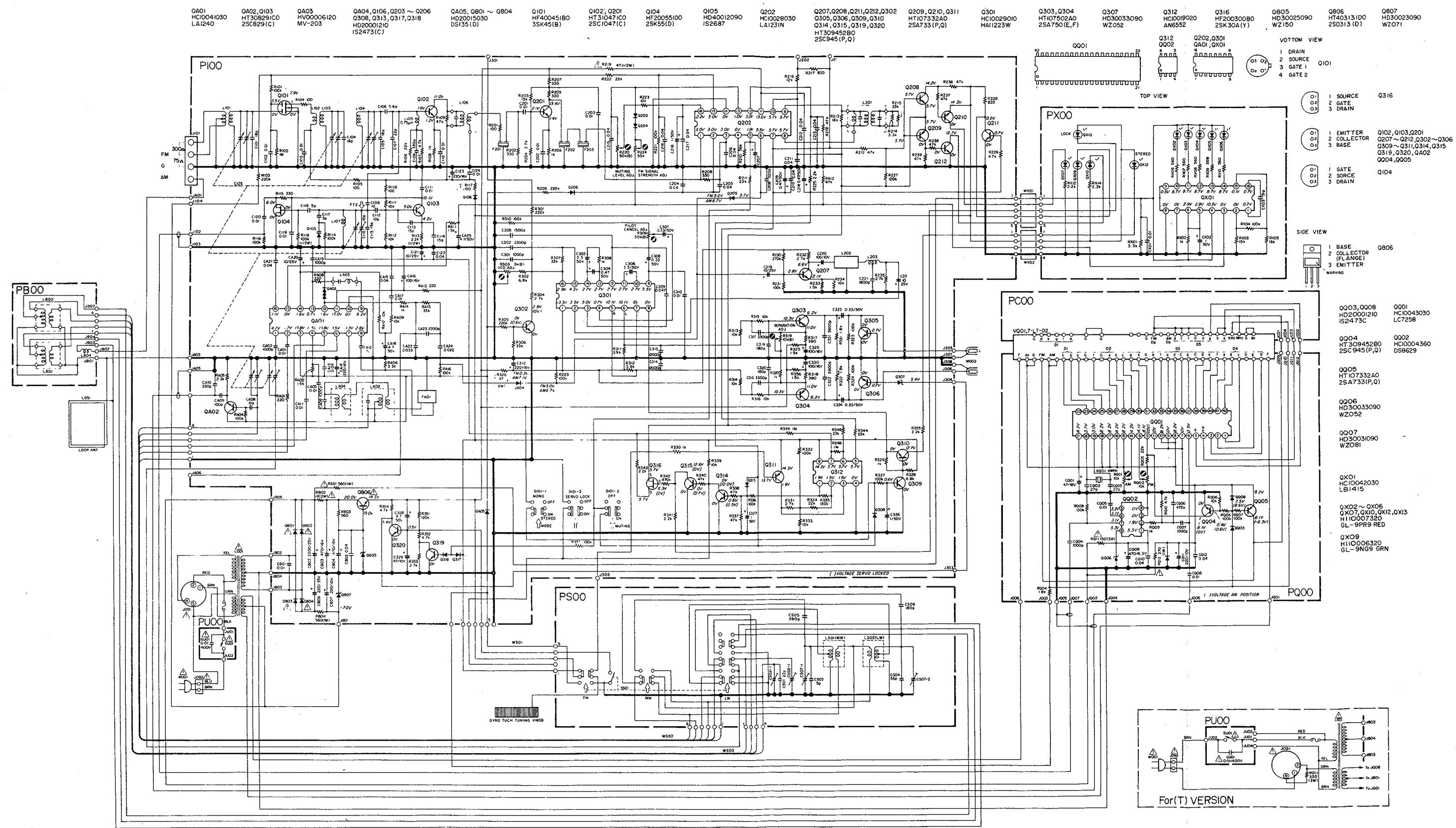
Components and wiring are subject to change for modification without notice.
NOTE ON SAFETY:
The parts marked with are important parts on the safety. Please use the parts having the designated parts numbers without fail.

- SERVICE MANUAL
- MARANTZ DESIGN AND SERVICE
- ORDERING PARTS
- OVERSEAS PARTS ORDERING
- CANADA
- AUSTRALIA
- JAPAN
- EUROPE
- TABLE OF CONTENTS
- SECTION
- MODEL ST450L LW/MW/FM STEREOPHONIC TUNER
- INTRODUCTION
- P.W. BOARDS
- TEST EQUIPMENT REQUIRED FOR SERVICING
- BLOCK DIAGRAM
- ALIGNMENT PROCEDURES
- FM Alignment Procedures (Function switch in the "FM" position)
- Muting Circuit Alignment
- Multiplex Alignment Procedures (Function switch in the "FM" position)
- AM Alignment Procedures
- Frequency Display Alignment Procedures
- FM Alignment
- MW Alignment
- VOLTAGE CONVERSION
- EUROPEAN MODEL ONLY
- CAUTION
- NOTE ON SAFETY:
- FTZ REGULATION
- DIAGRAM AND COMPONENT LOCATIONS
- TECHNICAL SPECIFICATIONS
- FM TUNER SECTION
Marque : MARANTZ
Modèle : ST 450 L
Catégorie : Récepteur audio-vidéo