DSP-223 - Radio Telex - Free user manual and instructions
Find the device manual for free DSP-223 Telex in PDF.


| Product Type | Tone-Remote Adapter for two-way radio base stations |
| Brand/Model | Telex DSP-223 |
| Dimensions | 8 1/2" W x 7 1/8" D x 1 5/8" H |
| Power Supply | 12 to 16 Vdc, 500 mA |
| Operating Temperature | 0 to 70°C |
| Key Functions | PTT relay, Monitor relay, F1 and F2 relays, 6 digital outputs, CTCSS generation (64 frequencies), Morse code encoder, DTMF responder, AGC, pre-emphasis, 3.5 kHz low-pass filter |
| Line Interface | 600-ohm balanced, 2-wire or 4-wire |
| Radio Interface | ±45 Vdc withstand rating, 6-pin connector and DB25 |
| Remote Console Compatibility | Vega tone remote consoles and others using sequential tone-keying |
| Function Tone Mode | Single (16 tones) or dual (100 tones) |
| CDCSS / CTCSS Frequencies | 64 selectable frequencies |
| Audio Frequency Response | ±1.5 dB, 300 to 3000 Hz |
| Notch Filter | 45 dB minimum rejection at 2175 Hz |
| Relay Contact Ratings | 1A at 125 Vac |
| Non-Relay Outputs | Open collector, active low, 200 mA max, 40 V |
| Warranty | 3 years limited |
| Repairability | Factory service center; schematics and parts lists provided in manual |
| Maintenance | Adjust level potentiometers, clean with dry cloth, no liquids |
| Safety Notes | Transient protected audio lines; do not apply DC to line transformers |
| Programming | Via RS-232 front panel port with Windows application |
Frequently Asked Questions - DSP-223 Telex
User questions about DSP-223 Telex
0 question about this device. Answer the ones you know or ask your own.
Ask a new question about this device
Download the instructions for your Radio in PDF format for free! Find your manual DSP-223 - Telex and take your electronic device back in hand. On this page are published all the documents necessary for the use of your device. DSP-223 by Telex.
USER MANUAL DSP-223 Telex
Operating Software 2.6
Technical Manual

natural_image
Black VEGA DSP-223 electronic device with coiled cable, showing ports and a handheld device (no readable text or symbols beyond branding)Table of Contents
1 General.... 1
1.1 DSP-223 Accessories....1
2 Installation 2
2.1 DSP-223 Power Supply 2
2.2 DSP-223 to Console Line Connection 2
2.3 DSP-223 to Radio Connection....2
2.3.1 TX Audio Connection.... 2
2.3.2 RX Audio Connection .... 3
2.3.3 PTT Connection....3
2.3.4 Monitor Connection .... 3
2.3.5 Radio Frequency Control....4
2.3.6 CTCSS Connection 4
2.4 Handset Connection....4
2.5 Digital Expansion Port 4
3 Level Settings....5
3.1 Line Receive Level Adjust Procedure 5
3.1.1 Revision G PCB's with J17 5
3.2 Radio TX Level Adjust Procedure....6
3.3 Radio RX Level Adjust Procedure 6
3.4 Line TX Level Adjust Procedure 6
3.5 CTCSS Level (Continuous Tone coded Squelch)....6
3.6 DSP -223 Detection Frequencies 6
4 Programming and Operation 7
4.1 Software Installation 7
4.2 Windows® Application Software Operation 7
4.2.1 Select a Serial Port....7
4.2.2 DSP-223 Configuration....8
4.2.2.1 Function Tone Mode....8
4.2.2.2 CTCSS Tone 8
4.2.2.3 PTT Options 8
4.2.2.4 Monitor Relay Options 9
4.2.2.5 EE/Error Beeps (Rev 2.0 or higher)....9
4.2.2.6 Line DTMF Decoder 9
4.2.2.7 Audio Loop Back 9
4.2.2.8 Individual Function Tone Setup 10
4.2.2.8.1 Tone Active 10
4.2.2.8.2 Relay....10
4.2.2.8.3 Relay Group....10
4.2.2.8.4 Relay Duration 10
4.2.2.8.5 Digital Output 11
4.2.2.8.6 CTCSS Frequency and Default....11
4.2.2.8 DIG4 Setup Button 12
4.2.2.9 DIG5 Setup Button 13
4.2.2.9.1 Voter/Ring Down Tone Generation 13
4.2.2.10 Set Gains Button 13
4.2.2.11 Morse Code Station Identifier Setup.... 14
4.2.2.12 Save and Load Buttons 14
4.2.2.13 Send and Receive Configuration from DSP-223 14
4.2.2.14 Radio TX Audio Filters 15
4.2.2.15 DSP-223 Audio Block Diagram.... 16
4.2.2.16 DSP-223 Frequency Response 16
4.3 DTMF Responder Functions.... 18
5 Theory of Operation....19
5.1 DSP-223 Audio Input Paths.... 19
5.2 DSP-223 Audio Output Paths....19
5.3 Troubleshooting Aid....19
6 Loading the DSP-223 Operational Software 20
7 Specific Radio Control.... 20
8 Pin out and Jumper Settings Quick Reference Table...... 21
9 Schematics and Parts Lists 22
9.1 PCB P/N 750561 Revisions A to E 22
9.2 PCB P/N 750561 Revision F 23
9.3 PCB P/N 750561 Revision G 24
9.4 PCB P/N 750561 Revision H 25
10 Warranty, Service, Repair, and Comments.... 26
11 DSP-223 Specifications 27
Table of Figures
Figure 1 DB25 Rear Connector Pin-out....2
Figure 2 Line Connector Pin-out .... 2
Figure 3 6 Pin Radio Connector Pin-out....3
Figure 4 Windows Programming Main Screen 7
Figure 5 Serial Communications Port Screen 7
Figure 6 Digital Output Chart....11
Figure 7 CTCSS Selection Chart ...... 12
Figure 8 Digital 4 Setup Screen 12
Figure 9 Digital 5 Setup Screen 13
Figure 10 Gain Settings.... 13
Figure 11 Morse Code Encoder Setup Screen....14
Figure 12 TX Audio Parameters Screen.... 15
Figure 13 Software Audio Path Block Diagram 16
Figure 14 Tx Frequency Response With No Additional Filtering....16
Figure 15 Tx Frequency Response With 3.5KHz Low Pass Filter....17
Figure 16 Tx Frequency Response With 3.5KHz Filter and Pre-Emphasis....17
1 General
Unless noted, this manual refers to DSP-223 operating software 2.6.
The VegaDSP-223 tone-remote adapter provides remote control of two-way-radio base stations using any Vega tone remote consoles. The DSP-223 is also compatible with other consoles using the industry-standard sequential tone-keying format.
The DSP-223 connects to the tone remote control console(s) using any voice-grade transmission medium such as a microwave link, a leased telephone line, or a twisted-pair 600-ohm line.
All DSP-223s are capable of decoding the PTT (push-to-talk/transmitter-on) tone sequence and the voice-plus-tone signals during transmission. Control tones in the voice-plus-tone signal are filtered from the transmitted voice. All models are prepared for jumper-plug conversion from two-wire-line operation to four-wire-line operation. In the four-wire mode, the panels are full duplex capable.
The DSP-223 provides the following features:
PTT Relay
Monitor Relay
99-digit display
PTT, Monitor, and Power LED indications
F1 and F2 Relays (programmable to any function tone or Revert to F1)
6 digital outputs for channel selection, completely programmable per function tone
CTCSS generation (64 frequencies)
Hardware and software gain control
Local handset port for monitoring activity and transmission back to base or to radio
Front panel test points and level set potentiometers
RS-232C port on front panel for configuration via Windows application
Two PTT modes and three monitor modes
Eight selectable PTT frequencies
Ability to pass-through to a second tone adapter with 400ms built in delay line
Relays can be placed in any of four groups for separation of function
Single Function tone recognition (16 function tones)
Dual function tone recognition (100 function tones)
Morse Code Encoder for Automatic station identification
Automatic Gain Control
Function Tone lock-out
RX Audio Squelch
Voter Status Tone
Alarm Beeps
Pre-Emphasis
3.5kHz Low Pass Filter
All audio inputs and outputs are transient protected.
The DSP-223 line transformers are not designed to operate on lines carrying direct current. If a DC voltage is on the line, isolate with external capacitors. If the line termination must conduct direct current, install a 600:600-ohm transformer designed for the current involved.
1.1 DSP-223 Accessories
Several optional accessories are available for the DSP-223.
DSP223PRG – Programming Kit, includes cable and diskette with software
DSP223RACK - 1 unit high rack shelf to hold up to two DSP-223 units
0101239 - DSP-223/Relm Serial Interface Kit
650373 - DSP-223 DB25 Relm Radio Cable
301896000 - DSP-223/Kenwood x150/x180 Serial Interface Kit
2490248 - Black Handset
2 Installation
2.1 DSP-223 Power Supply
The DSP-223 requires a 12 to 16 volt DC, 500 mA, of clean power. Two connectors are provided to connect the unit to power. The first is a 2.5mm plug receptacle on the rear left of the unit. The positive terminal is the center conductor. The second power connection option is the DB25 connector. Figure 1 shows the pin out of this connector. Connect an external 12 to 16 volt DC supply with the positive connected to Pin 20 and the Ground connected to Pin 7.

Figure 1 DB25 Rear Connector Pin-out
2.2 DSP-223 to Console Line Connection
The line connector is the right most connector on the rear of the DSP-223. Connect the two-wire leased
line to pins 4 and 5 of the RJ-45 modular connector, making sure that J20 and J21 are set to position A. Four-wire operation requires J20 and J21 be set to position B and connect the outgoing line to pins 4 and 5, and the receive pins to 3 and 6.
Note: Pins 4&5 of the Line connector are the RX audio from the radio. They are transmitted back down the line to the console. Pins 3&6 of the Line connector are inputs from the console and the audio present on this pair will be sent to the radio.

Figure 2 Line Connector Pin-out
There are several jumper selections that must be made for the line connection. Set the jumpers according to your connection requirements.
2 Wire / 4 Wire Selection: J20 J21 RX Termination: J19
| 2 Wire | A | A | 600 Ohms | A |
| 4 Wire | B | B | 10k Ohms | B |
The RX termination should be placed in position "A" on J19 for a single unit at the end of a line. If multiple units are connected in parallel, only one unit should have the RX Termination jumper in the "A" position. Set J19 to "B" position for 2-wire operation.
2.3 DSP-223 to Radio Connection
2.3.1 TX Audio Connection
The DSP-223 has a number of options when connecting it to the radio. Set the jumpers according to the method outlined in your radio's owner manual.
Connection Type: J14 J15 J22 J23
Single Ended Low-Impedance: A A A A
If the microphone input of the radio is high-impedance, shielded cable is recommended. If the radio has a high-level microphone input, move J26 to the B position, otherwise J26 should stay in the A position.
The balanced 600-Ohm option is only available on the DB25 connector on the rear panel; see Figure 1 for the pin-out. If the TX Audio is set to single ended mode, it can be used from the TX+ pin on the DB25 or can be accessed on the smaller 6-pin rear connector. The 6 Pin connector pin-out appears in Figure 3.

Figure 3 6 Pin Radio Connector Pin-out
2.3.2 RX Audio Connection
Set the following jumpers for the type of receive audio required:
Output Type: J24 J25 J27
Receive Input Impedance: J12 J13
8 Ohms A B (for a speaker output)
600-Ohm B A
10k Ohm B B
Connect the radio receiver audio output if balanced to pins 12 and 24 of the rear panel DB25. If the receive audio is single ended pin 24 of the rear DB25 or pin 4 of the rear 6 pin connector can be used. The audio source must be after the squelch circuit, to prevent sending continuous noise to the remote console. If a high-impedance point in the receiver is used, shielded cable is recommended.
Note: When the speaker output is used, the radio volume control will affect the audio levels of the DSP-223.
2.3.3 PTT Connection
Connect the radio PTT circuit to the PTT relay contact terminals. Connections on the DB25 or the 6 pin connectors may be used. Usually the common of the relay contact switch is grounded and the normally open contact connects to the PTT input. It is also possible to ground the common of the relay internal to the unit by bridging the pads of JP2 with wire and soldered closed.
2.3.4 Monitor Connection
Connect the radio MON circuit to the MON relay contact terminals of the DB25 connector. Usually the common of each relay contact switch is grounded and the normally open contact connects to the MON input. It is also possible to ground the common of the relay internal to the unit by bridging the pads of JP3 with wire and soldered closed.
2.3.5 Radio Frequency Control
The DSP-223 provides two relays that may be used for radio channel control. F1 and F2 contacts may be connected through the rear DB25 connector. Usually the common of each relay contact switch is grounded and the normally open contact connects to the radio frequency-control terminals.
In addition to the two standard relay closures, six lines of digital I/O are available. These lines are open-collector transistor outputs. They can be programmed on a per line basis to generate any of 64 combinations. A programmed option is also available that does not change the digital I/O.
Each line is active low and may be jumper selected to pull up to either +5v or the power supply voltage (minimum +12v). Jumper J16 is used to select the pull up voltage. The A position pulls to the power supply value and B pulls up to +5v.
Refer to Section 4.2.2.9.5 Digital Output for programming the digital outputs.
2.3.6 CTCSS Connection
The DSP-223 is designed to generate a full range of CTCSS frequencies. Each function tone can be assigned its own CTCSS frequency for PTT operation or a number of CTCSS tones can be set using different function tones. A single ended, capacitor coupled, low impedance output is available on pin 11 of the rear panel DB25 connector.
2.4 Handset Connection
The Telex Handset (P/N 249248) may be connected to the DSP-223 to monitor receive and transmit audio. When the handset PTT switch is pressed, the DSP-223 will be key up the radio on the existing frequency and the handset microphone audio will be transmitted.
Pressing the PTT-IC button on the front panel provides an intercom connection between the DSP-223 and the tone remote console.
2.5 Digital Expansion Port
The Digital Expansion Port on the rear panel of the DSP-223 provides a second serial communications connection for use in controlling various base station radios. A plug-in serial add-on PCB must be installed to enable this connector. This port is configured as a function of the specific application and the data is restricted to the control of specific radios. It is not intended as a general communications port to a PC.
3 Level Settings
Once the unit is connected into the system, the level potentiometers can be set as shown in Table 1.
3.1 Line Receive Level Adjust Procedure
The line RX level is the first level that must be set because all of the tone decoding is based on this level. Connect an Oscilloscope, RMS voltmeter, or dBm meter to Ground (TP-12) and Line RX audio (TP-2) test
points on DSP-223.
Inject the known highest signal level into the line receive circuitry. An external generator or a console can generate this with a test tone capability. Using Table 1, find the value of the injected signal level in the left most column (Actual RX Input (dBm)).
In the case of the DSP-223 being connected as a standard tone remote, the MAX input +10dBm column shows the level to adjust the RX Line Potentiometer to. This assumes that the standard +10dBm Guard Tone will be used.
The DSP-223 must be tuned to allow this +10dBm signal to be decoded without overdriving the inputs (max 3.5Vp-p) of the Analog to Digital Converter (ADC). On the row of the injected signal level, find the column that matches the measurement units of the device attached to the Line RX level test points on the front panel. Adjust the Line RX Potentiometer (R68) until it is close to the value listed in the table. This will allow the unit to work over its entire range without saturating the ADC. Note that this measurement is a signal level measurement of the voltage that is supplied to the ADC used by the DSP to decode the various required tones.
| RX POT Setup for Vega DSP Based Products | ||||||||||
| Actual RX Input (dBm) | Max Input +10dBm Set RX To: | Max Input 0dBm Set RX To: | Direct Crossover dBm to Volts Table | |||||||
| Vrms Vpp | dBm Vrms | Vpp dBm | dBm Vpp | Vrms | ||||||
| 10 1.13 | 3.20 3 10 | 6.90 | 2.44 | |||||||
| 9 | 1.02 | 2.88 | 2 | 9 | 6.25 | |||||
| 8 | 0.92 | 2.60 | 1 | 8 | 5.60 | |||||
| 7 | 0.79 | 2.24 | 0 | 7 | 5.00 | |||||
| 6 | 0.74 | 2.08 | -1 | 6 | 4.50 | |||||
| 5 | 0.68 | 1.92 | -2 | 5 | 4.00 | |||||
| 4 | 0.62 | 1.76 | -3 | 4 | 3.60 | |||||
| 3 | 0.55 | 1.56 | -4 | 3 | 3.20 | |||||
| 2 | 0.51 | 1.44 | -5 | 2 | 2.88 | |||||
| 1 | 0.40 | 1.14 | -6 | 1 | 2.60 | |||||
| 0 | 0.36 | 1.02 | -7 | 1.13 | 3.20 | 3 | 0 | 2.24 | ||
| -1 | 0.33 | 0.92 | -8 | 1.02 | 2.88 | 2 | -1 | 2.08 | ||
| -2 | 0.29 | 0.81 | -9 | 0.92 | 2.60 | 1 | -2 | 1.92 | ||
| -3 | 0.26 | 0.74 | -10 | 0.79 | 2.24 | 0 | -3 | 1.76 | ||
| -4 | 0.22 | 0.63 | -11 | 0.74 | 2.08 | -1 | -4 | 1.56 | ||
| -5 | 0.20 | 0.56 | -12 | 0.68 | 1.92 | -2 | -5 | 1.44 | ||
| -6 | 0.18 | 0.52 | -13 | 0.62 | 1.76 | -3 | -6 | 1.14 | ||
| -7 | 0.16 | 0.46 | -14 | 0.55 | 1.56 | -4 | -7 | 1.02 | ||
| -8 | 0.14 | 0.41 | -15 | 0.51 | 1.44 | -5 | -8 | 0.92 | ||
| -9 | 0.13 | 0.37 | -16 | 0.40 | 1.14 | -6 | -9 | 0.81 | ||
| -10 | 0.12 | 0.34 | -17 | 0.36 | 1.02 | -7 | -10 | 0.74 | ||
| -11 | 0.11 | 0.30 | -18 | 0.33 | 0.92 | -8 | -11 | 0.63 | ||
| -12 | 0.10 | 0.28 | -19 | 0.29 | 0.81 | -9 | -12 | 0.56 | ||
| -13 | 0.09 | 0.25 | -20 | 0.26 | 0.74 | -10 | -13 | 0.52 | ||
| -14 | 0.22 | 0.63 | -11 | -14 | 0.46 | |||||
| -15 | 0.20 | 0.56 | -12 | -15 | 0.41 | |||||
| -16 | 0.18 | 0.52 | -13 | -16 | 0.37 | |||||
| -17 | 0.16 | 0.46 | -14 | -17 | 0.34 | |||||
| -18 | 0.14 | 0.41 | -15 | -18 | 0.30 | |||||
| -19 | 0.13 | 0.37 | -16 | -19 | 0.28 | |||||
| -20 | 0.12 | 0.34 | -17 | -20 | 0.25 | |||||
| Table Usage:1) Place a known signal level into the RX terminals of the Vega device being setup.2) Determine the maximum signal level that the device will see. This table supports +10 and 0 dBm3) Using the values from #1 and #2, Lookup #1 in the left column and move to the grouping for #24) Set the RX pot for the value in the table | ||||||||||
Table 1
3.1.1 Revision G PCB's with J17
Starting with PCB Revision G, jumper J17 has been added to provide a wider decode range. With J17 in the "A" position the DSP223 will perform like previous versions. When J17 is in the "B" position, a 6dbm gain is added to the input of the ADC after PTT is engaged.
Setup is different with J17 in "B". When the DSP223 is in PTT, adjust the Line RX Potentiometer (R68) for -15dbm at Line RX audio (TP-2) test point.
3.2 Radio TX Level Adjust Procedure
Due to the large range of input requirements for the radios that can be connected to the DSP-223, there is not a prescribed way of setting the Radio TX levels. Radio TX test points (TP-5 & TP-6) on the front panel of the DSP-223 provide a location to measure the actual value being placed onto the radio TX inputs. The Radio TX gain potentiometer (R7) can be used to adjust these levels. Note if the unit is placed into single ended mode with jumpers J14, 15, 22, and 23 the Radio TX+ should be measured with respect to ground. The user also has the option of placing J26 into the "A" position to decrease the output of the TX line by a factor of 10. The final adjustment should allow for undistorted audio to be transmitted for the full range of transmission levels at the desired deviation. Soldering JP6 together will increase the radio TX output adjustment range.
3.3 Radio RX Level Adjust Procedure
The Radio RX level input to the DSP-223's ADC can be measured by connecting an Oscilloscope or Meter to the ground and Radio RX test jack (TP-3) on the front of the unit. The maximum expected receive level should be set so that the measurement at the test points is approximately 3.4 volts peak-to-peak or 1.2 volts RMS. This insures that the receive audio from the radio will not overdrive the input circuitry of the DSP-223. The usage of Table 1 can help facilitate this by following the directions for setting the Line RX levels. If the radio will not be generating a level above 0dBm, the 5-7 columns of the table can be used with a known input value to set the maximum level seen by the ADC. If the radio max level output will be below 0 dBm the Radio RX (R98) gain can be set higher to accommodate this.
3.4 Line TX Level Adjust Procedure
The Line TX level is the last item that should be adjusted. With the unit connected to the 600 Ohm line, connect an oscilloscope, meter reading true RMS, or a meter with an output in dBm to the Line TX test points (TP-7 & TP-8) on the front of the DSP-223. There are three ways to generate the required test tone for setting the levels. The easiest is to "double click" the IC PTT button on the front panel. A 1-minute 0dBm test tone will be sent on the Line and Radio TX lines. Pressing the IC PTT button again during the tone output will turn off the output. The second option, with the receive levels already set and a console capable of generating DTMF tones onto the Line RX pair, press "*0#8". A 15 second, 1kHz, 0dBm tone will be placed on the TX line pair. The third method to generate the tone is to move the test jumper, J11 to the "B" position. As long as the test jumper is in the "B" position, a 0dBm 1kHz tone will be placed on the TX line pair. This does require opening the case. Adjust the Line TX Potentiometer (R12) until the measured voltage is 2.2 Volts peak-to-peak, 0.77 volts RMS, or 0dBm. Soldering JP7 together will increase the Line TX output adjustment range.
3.5 CTCSS Level (Continuous Tone coded Squelch)
The CTCSS Level can be measured by connecting an oscilloscope or RMS meter to the ground and CTCSS test point (TP-13) on the front of the DSP-223. With the radio connected to the CTCSS output, have the remote console key up so that CTCSS is present. Adjust the CTCSS Potentiometer (R149) until the level is as desired.
3.6 DSP-223 Detection Frequencies
The DSP-223 has been factory-tuned to the following frequencies. The user of the DSP-223 has no ability to change the detection frequencies as they are coded into the software. However any actual function or output can be made to work with any existing programmed frequency. Please consult the factory for special requirements for frequency selections.
Guard tone/PTT Tone: 2175 Hz
MON Function Tone: 2050 Hz
Frequency Select Function Tones (where used)
| F1: 1950 Hz | F5: 1550 Hz | F9: 1150 Hz | F13: 750 Hz |
| F2: 1850 Hz | F6: 1450 Hz | F10: 1050 Hz | F14: 650 Hz |
| F3: 1750 Hz | F7: 1350 Hz | F11: 950 Hz | F15: 550 Hz |
| F4: 1650 Hz | F8: 1250 Hz | F12: 850 Hz | F16: 450 Hz |
4 Programming and Operation
All programming for the DSP-223 is through an RS-232C serial port located on the front panel of the unit. Programming kit (P/N DSP223PRG) may be purchased separately from the DSP-223 and installed on a Windows 95 or newer computer. The latest DSP-223 operating software and Windows® application may also be down loaded from www.vega-signaling.com/dspsoftware.htm
4.1 Software Installation
The Windows® application file is included on the VEGA Product Information CD provided with the DSP-223. Launch the CD and click on Firmware – then click on DSP-223. Follow the instructions for saving the file to the PC. When the application starts, an opening screen as shown in Figure 4 should appear.
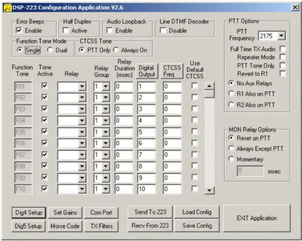
Figure 4 Windows Programming Main Screen
4.2 Windows® Application Software Operation
4.2.1 Select a Serial Port
Clicking Com Port on the main menu screen opens the dialog box shown in Figure 5. Select either Com1 or Com2 and then click OK to close the dialog box. The Windows® application will set the serial port configuration. A 9 pin serial cable is provided to connect the DSP-223 and the PC.
NOTE: The selected port is not saved and will default to Com1 each time the software is run.

Figure 5 Serial Communications Port Screen
4.2.2 DSP-223 Configuration
Each button and programming field is described in the sections that follow.
4.2.2.1 Function Tone Mode
In the upper left corner is a selection for single or dual function tone mode. Single function tone mode requires that the controlling console generate its Guard tone and then a single 40ms function tone. Dual function tone mode requires that the controlling console generate the Guard tone and then two consecutive function tones, which are then combined to form a 00-99 function tone. The standard function tones and their frequencies are shown in the following table.
| Function Tone Number | Frequency (Hz) | Function Tone Number | Frequency (Hz) |
| F1 | 1950 | F9 | |
| F2 | 1850 | F10 | |
| F3 | 1750 | F11 | |
| F4 | 1650 | F12 | |
| F5 | 1550 | F13 | |
| F6 | 1450 | F14 | |
| F7 | 1350 | F15 | |
| F8 | 1250 | F16 |
Dual function tones use tones F1-F10 and construct the final function tone value by combining the first received tone as the tens digit and the second received tone as the ones digit. F10 is used as a zero. For example: Function tone 9 would be transmitted as F10-F9, Function tone 43 would be F4-F3, and so forth.
It is very important that DSP-223 be programmed for the type of signaling that is being sent from the controlling consoles. It is possible to put the unit into the dual tone mode and send single tones and have it recognize them correctly. This mode is more prone to errors however. The best way to make this work is to make certain that no tones are sent for 40ms after the first function tone is sent so that a no tone can be decoded. If the 2175 hold tone, or other audio is present, the DSP-223 will attempt to decode this as the second half of the dual function tone.
The DSP-223 will also error beep back to the console if it was unable to decode a function sequence from the console. This consists of a short sequence of 3-4 beeps.
Selecting single or dual function tone mode will set the number of function tones that can be programmed by scrolling in the data entry table between 16 and 100 respectively.
4.2.2.2 CTCSS Tone
Two options are provided to set the CTCSS operation. PTT Only sets the CTCSS generator active during PTT detection only. Always On sets the CTCSS tone generator active at all times regardless of the PTT status.
4.2.2.3 PTT Options
The PTT Options Section configures the DSP-223 while PTT is active. These options control the PTT relay, R1 and R2 relays with respect to PTT, the received console PTT frequency as well as the PTT mode.
PTT Frequency selects the Hold tone frequency received from the console. The selectable frequencies are:
| 2100 Hz | 2325 Hz |
| 2155 Hz | 2600 Hz |
| 2175 Hz | 2800 Hz |
| 2300 Hz | 2970 Hz |
The Repeater Mode introduces a 400ms audio delay in the transmit path and removes the Hold tone notch filter. If the unit detects a valid Guard-Function sequence, it will key up the DSP-223 immediately. With the 400ms delay, the Guard Function is repeated out the radio interface. If the DSP-223 detects the Hold tone, it will remain keyed up allowing one radio to serve as the link to another DSP-223.
PTT Tone Only causes the DSP-223 to not respond to a function tone and key up on detection of a valid Hold tone. This will eliminate all options that are function tone based, but allows the DSP-223 to be used in a most basic manner. This mode is useful for alignment when only a single tone generator is available and not a tone remote console
Revert to R1 energizes relay R1 at the end of a PTT sequence. It will either latch it on or energize it for the time programmed for R1 in the function tone table. For example, if F1 uses R1 and has a timer setting of zero, the Revert to R1 option will latch the R1 relay at the end of the PTT sequence. If F1 has R1 selected and has a timer value set for R1, then at the end of the PTT, R1 will latch on for the timer value and then turn off. Note that all function tones that utilize R1 must have the same timer value setting. The setup software enforces this by changing all values for R1 when one is changed.
The operation of auxiliary relays R1 and R2 as a function of PTT is selectable. When selected, R1 or R2 will close at the same time as the PTT relay. Connection to the relay contacts may be made through the DB25 connector on the rear panel. No auxiliary relay operation may also be selected.
4.2.2.4 Monitor Relay Options
The MONITOR function provided in the DSP-223 decodes the valid tone sequence and provides a relay-contact closure to turn off the sub-audible-tone-decoder circuit in the radio receiver, allowing the console operator to monitor the channel for other users before transmitting (required by FCC regulations on stations equipped with continuous-tone-coded-squelch signaling). Connection to the monitor relay contacts is provided through the DB25 connector on the rear panel. On single-user stations not equipped with sub-audible signaling, or where the CTCSS decoders are disabled, the monitor function relay output may be used for any purpose such as interrogation of a status-reporting system at the station site. The monitor function may be programmed to operate in one of three modes.
The DSP-223 provides three options for the MONITOR relay action. Reset on PTT resets the monitor relay when PTT goes active. Always Except PTT latches the MON relay at all times except when PTT is active, whether the monitor function tone is received or not. Momentary sets the monitor relay for a programmed period of time.
4.2.2.5 EE/Error Beeps (Rev 2.0 or higher)
The DSP223 will display "EE" on the front panel LED display and transmit error beeps to the dispatch console when an un-decodable signal is received on the line RX. To defeat the error beep feature uncheck the checkbox.
4.2.2.6 Line DTMF Decoder
When checked, the DSP-223 will not respond to DTMF tones sent by the console.
4.2.2.7 Audio Loop Back
When checked, the DSP-223 will route all audio received at the Line RX terminals back to the Line TX terminals. In addition all functions continue to work within the DSP-223. This allows for a number of consoles to be bridged together and still monitor traffic of consoles on separate bridge segments. This function is typically used in 4-wire systems only.
4.2.2.8 Individual Function Tone Setup
The middle grid area of the main screen menu is used to set the actions of the DSP-223 when a particular function tone is received. The left most column is the function tone number. If the Function Tone Mode is set to single function tone, tones F1-F16 may be programmed. If the Function Tone Mode is for dual function tone, tones F00-F99 may be programmed.
4.2.2.8.1 Tone Active
The Tone Active column allows the user to lockout a function tone in the DSP223. When a box is checked, the DSP-223 will respond to the selected function tones and operate as programmed.
4.2.2.8.2 Relay
The Relay column allows the user to select a relay closure to be associated with a particular function tone. Selectable options are R01, R02, or no relay. Clicking the drop down list and selecting the desired relay will program the relay be closed immediately upon receipt of the function tone.
NOTE: R01 = F1 and R02 = F2 with reference to the schematic.
4.2.2.8.3 Relay Group
The Relay Group allows the relays to be grouped into separate functions. This sets more than one relay to be energized at any particular time by assigning separate groups. For example, if F1 has R1 selected as its relay, and F2 has R2 selected as its relay, setting the two Relay Group numbers to the same value will result in: when F1 is received R1 turns on and R2 turns off. In this scenario, F1 and F2's relays are interlocked. If F1 and F2 have different assigned relay groups, receiving F1 does not turn off R2. Further, if a function tone has no relay selected, but has a relay group assigned that is used by another relay group, when that function is received, all relays in that group will be turned off. This allows R1 and R2 to be assigned to different groups and use other function tones with the same relay group to turn them off.
4.2.2.8.4 Relay Duration
The Relay Duration sets the relay closure time. When a function tone is received, the relay closes. After the time expires, the relay will open. The timer entry is in milli seconds (i.e. 1000 mSec = 1 second). Setting the relay duration to 0 latches the relay on when the function tone is received.
CAUTION: two function tones with the same relay assigned cannot have the relay close for different durations. Therefore, if the user selects R1 for F1 and F6 and set the duration for F1 to 2000ms, the F6 relay duration entry will automatically be set to 2000ms by the application software.
4.2.2.8.5 Digital Output
Each function tone may be assigned a digital output. Valid entries are 0 - 64 that control the outputs labeled DIG0-DIG5. This is a binary output corresponding to the value entered. The table below shows the values and the resulting DIG0-DIG5 outputs.
An entry of 64 will cause the digital outputs to REMAIN SET at the current value and not change.
| VALUE | D5 | D4 | D3 | D2 | D1 | D0 | VALUE | D5 | D4 | D3 | D2 | D1 | D0 |
| 0 | L | L | L | L | L | L | 32 | H | L | L | L | L | L |
| 1 | L | L | L | L | L | H | 33 | H | L | L | L | L | H |
| 2 | L | L | L | L | H 34 | H | L | L | L | H | L | ||
| 3 | L | L | L | L | H 35 | H | L | L | L | H | H | ||
| 4 | L | L | L | H | L | L 36 | H | L | L | H | L | L | |
| 5 | L | L | L | H | L | H | 37 | H | L | L | H | L | H |
| 6 | L | L | L | H | H | 38 L | H | L | L | H | H | L | |
| 7 | L | L | L | H | H | ||||||||
| 8 | L | L | |||||||||||
| 9 | L | ||||||||||||
| 10 | L | ||||||||||||
| 11 | L | ||||||||||||
| 12 | L | ||||||||||||
| 13 | L | ||||||||||||
| 14 | L | ||||||||||||
| 15 | L | ||||||||||||
| 16 | L | ||||||||||||
| 17 | L | ||||||||||||
| 18 | L | ||||||||||||
| 19 | L | ||||||||||||
| 20 | L H L H H H H H H H H H H H H H H H H H H H H H H H H H H H H H H H H H H H H H H H H H H H H H H H H H H H H H H H H H H H H H H H H H H H H H H H H H H H H H H H H H H H H H H H H H H H H H H H H H H H H I I I I I I I I I I I I I I I I I I I I I I I I I I I I I I I I I I I I I I I I I I I I I I I I I I I I I I I I I I I I I I I I I I I I I I I I I I I I I I I II II II II II II II II II II II II II II II II II II II II II II II II II II II II II II II II II II II II II II II II II II II II II II II II II II II II II II II II II II II II II II II II II II II IIIIIIIIIIIIIIIIIIIIIIIIIIIIIIIIIIIIIIIIIIIIIIIIIIIIIIIIIIIIIIIIIIIIIIIIIIIIIIIIIIIIIIIIIIIIIIIIIIIIIIIIIIIIIIIIIIIIIIIIIIIIIIIIIIIIIIIIIIIIIIIIIIIIIIIIIIIIIIIIIIIIIIIIIIIIIIIIIIIIIIIIIIIIIIIIIIIIIIIIIIIII III III III III III III III III III III III III III III III III III III III III III III III III III III III III III III III III III III III III III III III III III III III III III III III III III III III III III III III III III III III III III III III III III III III III III III III III III III III III III III III III III III III III III III III III III III III III III III III III IIIIIIIIIIIIIIIIIIIIIIIIIIIIIIIIIIIIIIIIIIIIIIIIIIIIIIIIIIIIIIIIIIIIIIIIIIIIIIIIIIIIIIIIIIIIIIIIIIIIIIIIIIIIIIIIIIIIIIIIIIIIIIIIIIIIIIIIIIIIIIIIIIIIIIIIIIIIIIIIIIIIIIIIIIIIIIIIIIIIIIIIIIIIIIIIIIIIIIIIIIIIIIIIIIIIIIIIIIIIIIIIIIIIIIIIIIIIIIIIIIIIIIIIIIIIIIIIIIIIIIIIIIIIIIIIIIIIIIIIIIIIIIIIIIIIIIII II II II II II II II II II II II II II II II II II II II II II II II II II II II II II II II II II II II II II II II II II II II II II II II II II II II II II II II II II II-II |
Figure 6 Digital Output Chart
NOTE: Digital output bits D4 or D5 are not active if DIG4 or DIG5 are enabled
4.2.2.8.6 CTCSS Frequency and Default
This value allows the user to set the CTCSS frequency for a given function tone. When the function tone is received, the CTCSS tone generator frequency is set to the value corresponding to the number entered. An entry of 0 corresponds to no tone. If the Use Default CTCSS checkbox to the right of the CTCSS Frequency box is checked (see Figure 4), the value in the CTCSS tone box is ignored and the last selected value is generated during PTT. For example, F1 is used for all transmissions and the default CTCSS box is checked for F1. F2-F8 has different CTCSS values programmed for them without
the CTCSS default box checked. Selecting F2 and then keying up on F1 will set the CTCSS tone to the value in the F2 row. Selecting F4 would set the CTCSS tone in the F4 row. When PTT is pressed, F1 is the default frequency and the F4 CTCSS tone is sent. Some consoles, such as the Vega C-1610 and 6124 have a paired mode that makes this operation very simple. The CTCSS tone lookup table appears below.
| Tone # Freq. (Hz) | Tone # Freq. (Hz) | Tone # Freq. (Hz) | Tone # Freq. (Hz) | Tone # Freq. (Hz) | |||
| 1 | 33.0 | 17 | 71.9 | 33 | 123.0 | 49 | 183.5 |
| 2 | 35.4 | 18 | 74.4 | 34 | 127.3 | 50 | 186.2 |
| 3 | 36.6 | 19 | 77.0 | 35 | 131.8 | 51 | 189.9 |
| 4 | 37.9 | 20 | 79.7 | 36 | 136.5 | 52 | 192.8 |
| 5 | 39.6 | 21 | 82.5 | 37 | 141.3 | 53 | 196.6 |
| 6 | 44.4 | 22 | 85.4 | 38 | 146.2 | 54 | 199.5 |
| 7 | 47.5 | 23 | 88.5 | 39 | 151.4 | 55 | 203.5 |
| 8 | 49.2 | 24 | 91.5 | 40 | 156.7 | 56 | 206.5 |
| 9 | 51.2 | 25 | 94.8 | 41 | 159.8 | 57 | 210.7 |
| 10 | 53.0 | 26 | 97.4 | 42 | 162.2 | 58 | 218.1 |
| 11 | 54.9 | 27 | 100.0 | 43 | 165.5 | 59 | 225.7 |
| 12 | 56.8 | 28 | 103.5 | 44 | 167.9 | 60 | 229.1 |
| 13 | 58.8 | 29 | 107.2 | 45 | 171.3 | 61 | 233.6 |
| 14 | 63.0 | 30 | 110.9 | 46 | 173.8 | 62 | 241.8 |
| 15 | 67.0 | 31 | 114.8 | 47 | 177.3 | 63 | 250.3 |
| 16 | 69.4 | 32 | 118.8 | 48 | 179.9 | 64 | 254.1 |
Figure 7 CTCSS Selection Chart
4.2.2.8 DIG4 Setup Button
This grouping allows the DSP-223 to mute the radio RX input in the event of an active logic signal on Pin 10 (DIG4) of the DB25 radio interface connector. Enable Dig4 as COR Input must be checked to enable the feature. Active High sets the polarity of the active logic signal. If checked, the radio RX will be muted when an active high is present and not muted when low.
The subset feature to polarity is the R1 and R2 check boxes. When one of these boxes is checked, that relay will close with the active state setting. The relay will also close from other programmed features. If RX Mute is in an active state when changing the programming to OFF, power to the DSP223 will have to be cycled to reset the RX audio path.
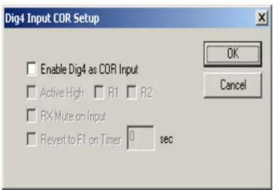
Figure 8 Digital 4
The fourth checkbox will force the DSP223 to revert to F1 programming after the entered time expires if no PTT or a COR logic changes occur.
NOTE: Digital output bits D4 or D5 are not active if DIG4 or DIG5 are enabled
4.2.2.9 DIG5 Setup Button
4.2.2.9.1 Voter/Ring Down Tone Generation
This grouping allows the DSP-223 to generate a user-defined tone on the Line TX pair in the event of an active logic signal on Pin 2 of the line connector or Pin-23 (DIG5) of the DB25 connector. Enable Tone on Dig5 Input must be checked to enable the feature. Active High sets the polarity of the active logic signal. If checked, the programmed tone will be generated when an active high is present and no tone will be generated when low.
The subset feature to polarity is the R1 and R2 check boxes. When one of these boxes is checked that relay will close with the active state setting. The relay will also close from other programmed features.
The Tone Frequency and Level boxes specify the frequency and the amplitude of the tone to be summed with receive audio. Entries of 300-3000Hz are valid. Typically a -20dBm signal is used. Some experimentation with this value may be required to get the proper performance.
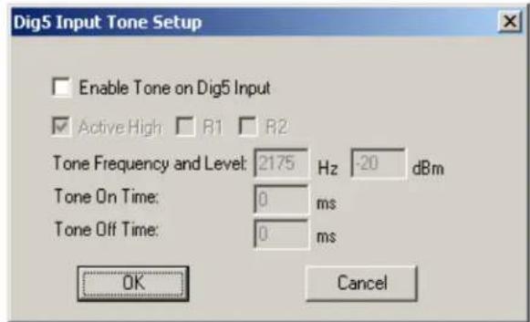
Figure 9 Digital 5
Tone On/OFF Time sets the duty cycle of the tone to create "alarm beeps" generated when DIG5 is active. Entries of 0 to 65000ms (65000ms = 65 seconds) are the allowed programmable times. An entry of zero (0) into the field generates a continuous tone.
NOTE: Digital output bits D4 or D5 are not active if DIG4 or DIG5 are enabled
4.2.2.10 Set Gains Button
Figure 10 at the right shows the Gain Set dialog box. A number of gains can be controlled with this setup application. This is not a replacement to tuning the unit correctly with the potentiometers, but a supplement to allow fine-tuning of the DSP-223 operation.
The Handset Sidetone Gain allows the volume of the handset speaker to be adjusted by +/- 10 dB. The Radio TX Gain allows adjustment of the amplitude of the audio sent to the radio by +/- 10dB. The Line TX Gain is used to adjust the Line TX by +/- 10dB. The CTCSS Gain allows adjustment of the CTCSS tone level by +/- 10dB.
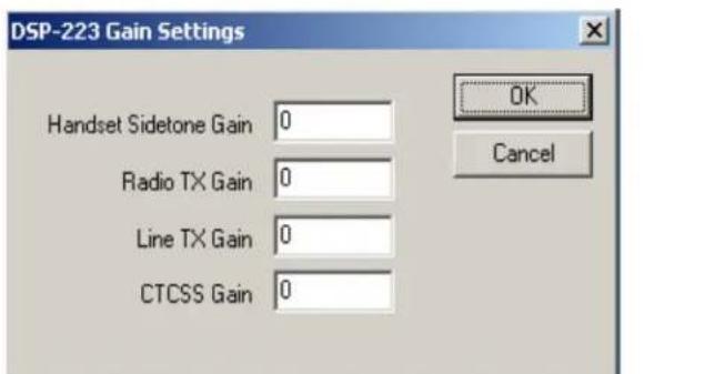
Figure 10 Gain Settings
4.2.2.11 Morse Code Station Identifier Setup
The Morse Code configures the DSP-223 to automatically send a Morse code signal at specified times or actions. The Auto Transmit Options section of the dialog box sets the automatic transmit operation.
The End of Each PTT will send the programmed Morse code string at the end of each PTT sequence. The DSP-223 waits for the end of the hold tone and then extends the PTT time to send the Morse code sequence. The Timer Interval option sets the DSP-223 to transmit the Morse code at specified time intervals. The timer begins running upon setup of this parameter either at power up or after programming. If the radio is keyed up when the timer expires, The DSP-223 will wait for the loss of hold tone and then add the Morse code sequence to the end of the transmission. Depending on the customers system, FCC requires that station identification be transmitted every 15 or 30 minutes of use. If the unit is not transmitting when the timer times out, no sequence will be sent. NOTE: The DSP-223 will not key up the radio to send the Morse code sequence.
The Morse Code Frequency sets the frequency of the Morse code tone. The FCC typically requires 1200Hz unless it would cause interference. Valid entries are from 400Hz to 2000Hz.

Figure 11 Morse Code Encoder Setup Screen
The Morse Code Gain sets the transmit level. Valid
values are from -40 to 0 dB. Use this value to set the deviation to the FCC required 40% level, based on your previous hardware gain settings.
Morse Code String specifies the string of up to 50 alphanumeric characters to be transmitted. Standard punctuation characters may also be entered.
NOTE: Programming the DSP-223 with a blank string disables the Morse code feature.
4.2.2.12 Save and Load Buttons
The user configuration data stored in a PC may be saved and reloaded into the Windows® application with the Save Config and Load Config buttons. This allows the configuration to be stored on a local hard disk or removable floppy disk.
NOTE: Configuration data MUST be compatible with the current Windows® application version
4.2.2.13 Send and Receive Configuration from DSP-223
The Send to 223 and Recv from 223 buttons are used to transfer configuration data between the DSP-223 and the PC. The serial port of the DSP-223 and the PC must be connected using the provided serial cable.
When all of the configuration information has been entered into the Windows® application, the data may be sent to the DSP-223 by pressing the Send to 223 button. The Recv from 223 button will retrieve the configuration data from the DSP-223 and display the information in the Windows® application. The user may then wish to save the data to a PC (refer to section 4.2.2.12).
If the data is transferred correctly the left decimal point will light for a few seconds and then turn off. If an error occurs, "EE" will appear in the display. The previously saved operation parameters will be restored.
4.2.2.14 Radio TX Audio Filters
The TX Filters button sets the options for controlling the radio TX audio.
4.2.2.14.1 AGC
The AGC checkbox adds an Automatic Gain Control or audio compression to the radio TX audio. AGC will help to increase the level of low audio, and decrease the level of loud audio, resulting in a more consistent level being transmitted.
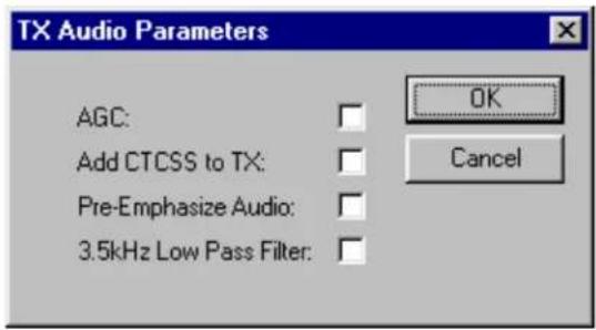
Figure 12 TX Audio Parameters Screen
4.2.2.14.2 Add CTCSS to TX
When checked, Add CTCSS to TX will add the selected
CTCSS tone to the TX audio stream. The CTCSS output (pin 11 of the DB25 connector) continues to be active. This allows CTCSS to be sent on radios that don't have separate input pin for its injection into the audio stream. The user will need to make certain that no high pass filter is in place in the radio to cut off the CTCSS audio.
4.2.2.14.3 Pre-Emphasize Audio
The Pre-Emphasis Audio option will add a pre-emphasis zero and pole into the radio TX audio stream. The frequency response can be seen in Figure 16
4.2.2.14.4 3.5kHz Low Pass Filter
The 3.5kHz Low Pass Filter attenuates frequencies above the cutoff frequency in the transmit audio stream. The frequency response can be seen in Figure 15
4.2.2.15 DSP-223 Audio Block Diagram
See the previous programming sections on inserting/removing the Pre-Emphasis, AGC, 3.5kHz Low Pass Filter, and the 400ms Delay options.

flowchart
graph TD
    A["Line RX Audio"] --> B["Notch Filter"]
    B --> C["Pre-Emphasis"]
    C --> D["AGC"]
    D --> E["+"]
    E --> F["3.5kHz Low Pass"]
    F --> G["Radio TX Audio"]
    H["Line TX Audio"] --> I["Notch Filter"]
    I --> J["Pre-Emphasis"]
    J --> K["AGC"]
    K --> L["+"]
    L --> M["3.5kHz Low Pass"]
    M --> N["Radio TX Audio"]
    O["CTCSS Generator"] --> P["CTCSS Audio"]
    Q["400ms Delay"] --> R["Tone Detectors"]
    S["Handset Speaker"] --> T["CTCSS Audio"]
    U["Radio RX Audio"] --> V["CTCSS Audio"]
Figure 13 Software Audio Path Block Diagram
4.2.2.16 DSP-223 Frequency Response

line
| Hz | dBm | | ---- | ---- | | 100 | -4.0 | | 200 | -2.0 | | 300 | -1.0 | | 400 | -0.5 | | 500 | -0.2 | | 700 | -0.1 | | 1k | -0.1 | | 2k | -38.0| | 3k | -1.0 | | 4k | -3.0 |Figure 14 Tx Frequency Response With No Additional Filtering

line
| Hz | d B m | | ---- | ----- | | 100 | -4.0 | | 200 | -2.0 | | 300 | -1.0 | | 400 | -0.5 | | 500 | -0.2 | | 700 | -0.1 | | 1k | -0.1 | | 2k | -38.0 | | 3k | -10.0 | | 4k | -40.0 |Figure 15 Tx Frequency Response With 3.5KHz Low Pass Filter

line
| Hz | dBm | | ---- | ---- | | 100 | -20 | | 200 | -15 | | 300 | -10 | | 400 | -5 | | 500 | 0 | | 700 | 5 | | 1k | 10 | | 2k | 5 | | 3k | 5 | | 4k | -40 |Figure 16 Tx Frequency Response With 3.5KHz Filter and Pre-Emphasis
4.3 DTMF Responder Functions
A number of DTMF sequences may be sent to the DSP-223 from the console that may be used to affect the performance of the unit or initiate a test function.
The standard activation sequence that precedes each command is DTMF *0#. A 2 second timer is started upon entry of the first character of the string. If the entire control string is not entered within that timeout period, the digits are discarded and the user must re-enter the string. For routines that adjust gains, the value is adjusted and saved to the non-volatile memory.
\*0#1 : Increase Radio TX Gain
Sending this command will increase the Radio TX gain by 1dB. Multiple repetitions of this sequence will increase the Radio TX Gain up to +10dB.
\*0#2 : Decrease Radio TX Gain
Sending this command will decrease the Radio TX gain by 1dB. Multiple repetitions of this sequence will decrease the Radio TX Gain down to -10dB.
\*0#3 : Increase Line TX Gain
Sending this command will increase the Line TX gain by 1dB. Multiple repetitions of this sequence will increase the Line TX Gain up to +10dB.
\*0#4 : Decrease Line TX Gain
Sending this command will decrease the Line TX gain by 1dB. Multiple repetitions of this sequence will decrease the Line TX Gain down to -10dB.
\*0#5 : Increase CTCSS Gain
Sending this command will increase the CTCSS gain by 1dB. Multiple repetitions of this sequence will increase the CTCSS Gain up to +10dB.
\*0#6 : Decrease CTCSS Gain
Sending this command will decrease the CTCSS gain by 1dB. Multiple repetitions of this sequence will decrease the CTCSS Gain down to -10dB.
\*0#7 : Loopback Line RX to Line TX
This command will place the DSP-223 into the Loopback Mode. Audio received at the RX terminals of the Line interface on the DSP-223 will be echoed back onto the TX terminals. This mode lasts for approximately 15 seconds and then the DSP-223 reverts back to its normal operation.
\*0#8 : Send 1kHz Tone to both Radio and Line Interfaces
This command will generate a 1kHz, 10dBm, tone on both the Radio and Line TX terminals. This can be used to set the DSP-223 TX level. The tone will last for approximately 15 seconds. There are no relay closures associated with this mode.
The following DTMF sequences are enabled for control of the Kenwood x150/x180 radio Refer to Section 7 – Specific Radio Control for Adaptor Kit Information
\*0#9 : Toggle SCAN Mode of the Kenwood x150/x180 Radio
This command will toggle the SCAN mode of the Kenwood x150/x180 Series radio on and off.
\*0#10 : Send the last Kenwood FleetSync® ANI data
This command causes the DSP-223 to generate a DTMF string to the Line TX corresponding to the last seven digit Kenwood FleetSync® ANI data received by the radio.
5 Theory of Operation
The DSP-223 is a Digital Signal Processor (DSP) based product. Many of the signals that once could be probed on older products, are handled within the DSP itself. This includes DTMF decoders, notch filters, tone decoders, and all of the audio summing. Most of the gain controls are also included within the software of the DSP. Because of this, hardware is simplified at the expense of software creation time and user serviceability. The next sections discuss the portions of the DSP-223 that can be tested using a common oscilloscope and voltage meter by a qualified service technician.
5.1 DSP-223 Audio Input Paths
The DSP-223 has only a single stereo Analog to Digital Converter (ADC) U25. The left channel converts the Line receive audio and the right channel converts the Radio receive audio. A CMOS switch, U2, is used to break those paths and insert handset audio for transmission down the line or to the radio. Up to the point of entry into the ADC, the audio is analog and handled by standard op-amps. These paths can be followed on the schematic and probed with any high-impedance measurement device.
5.2 DSP-223 Audio Output Paths
The DSP-223 has two stereo Digital to Analog Converters (DACs), U3 and U4. U4's left channel drives the sidetone for the handset. U4's right channel is used for the CTCSS tone generation. U3's left channel is the line transmit audio source and the right channel of U3 is the radios transmit audio source. Once the analog signal has been reconstructed on U3 and U4, they can be measured by conventional techniques.
5.3 Troubleshooting Aid
| Problem | Possible Solution | |
| What is position “A” on a jumper plug | On early PCB’s the “A” position of the jumper is the double line side of the silkscreen around the jumper plug. | |
| The DSP223 will not decode Is the Is J11 in the “A” position?If in 4-wire, make sure the consoleCheck telephone line continuity from dispatch console | the power LED on the front panel ON? | |
| TX is connected to the DSP223 line RX. | ||
| Ensure alignment procedure Section 3.1 of the manual is correct. | ||
| from dispatch console | ||
| Verify that proper PTT frequency is selected Section 4.2.2.5 of the manual (Rev 2.0 operating software or higher) | ||
| The DSP223 will not PTT radio Does PTT LED on front panel turn ON?Check for proper PTT relay configuration/clock to see if JP2 is soldered | guration/wiringclosed (if common is grounded) | |
| Verify that proper PTT frequency is selected Section 4.2.2.5 of the manual (Rev 2.0 operating software or higher) | ||
| Verify that function tone is not locked out Section 4.2.2.9.1 of the manual (Rev 2.0 operating software or higher) | ||
| Radio TX audio is low or distortedSet J26 to opposite position, rech | Check setup procedure Section 2.3.1 of the manual. | |
| Check alignment procedure Section 3.3 of the manual. | ||
| check. | ||
| EE and error beeps occur Overdriving of the Line RX ADC is occurring, adjust R68 down | ||
| Turn error beeps OFF, Section 4.2.2.11 of the manual (Rev 2.0 operating software or higher) | ||
| Radio RX audio is low or distorted | Check setup procedure Section 2.3.2 of the manual. | |
| Check alignment procedure Section 3.4 of the manual. | ||
| Check telephone line continuity to the dispatch console | ||
| Unable to decode DTMF | Check setup procedure Section 4.2.2.4 of the manual. | |
| The DSP223 will not Monitor function radioCheck for proper Monitor relay c | Does Monitor LED on front panel turn ON? | |
| configuration/wiring | ||
| Check to see if JP3 is soldered c | closed (if common is grounded) | |
| Unable to program DSP223 Verify | operating and programming software is the same revision. | |
| Download required files from web site www.vega-signaling.com and follow Section 6 of the manual to update DSP223 software. | ||
Check our web site for updated Troubleshooting aids.
6 Loading the DSP-223 Operational Software
1) The latest DSP-223 operating software and Windows® application software (and all previous versions) may be downloaded from www.vega-signaling.com/dspsoftware.htm
2) Copy all included files into a directory on your PC, if they are zipped, extract them into this directory
3) From the Start->Run, or Windows Explorer, menu run the file "winmon.exe". This file needs to be run only one time on a particular PC. It registers the drivers to communicate with the Vega products
4) Either on the desktop or from the taskbar editor, add a shortcut to the program "Flashmon.exe". Alternately it can be run from the Start->Run menu as well. The dialog box contains a few options that can be used.
5) The first step is to put the DSP-223 into programming mode. This is done by first removing power from the unit.
6) The upper left corner of the Flashmon dialog box has a pull down menu for setting the baud rate. The DSP-223 requires this value to be set to 19200. Change the baud rate to 19200.
7) With a straight through cable connected from the PCs Com1 port, (Com1 is the only option as of now) click the "Power On" button in the dialog box and then apply power to the DSP-223.
8) After a couple seconds, the message "Power is On" will appear in the message window of the dialog box. This indicates that communications has been established with the DSP-223 and that it is now ready to accept a software download.
9) Click on the "Program..." button. Find the file for the version of software to be flashed into the DSP-223. It will always have an extension of .BNM. Usually it will be of the form DSPVXX.BNM.
10) Double click or select the file and open it to begin the download process.
11) The verify button can be used the same way as the "Program..." button but it does not write to the flash, only verifies it.
7 Specific Radio Control
Operating software Version 2.6 enables the DSP-223 to control the Relm BK Series and Kenwood x150/x180 Series radios with serial commands from the Digital Expansion Port. If one of these radios is connected to the DSP-223 when power is applied, the DSP-223 will detect the presence of the radio and set the operating configuration. Standard radio control operations are PTT, monitor, and channel change (i.e. F1=channel 1, F2=channel 2, etc.). Power to the DSP-223 is provided by the radios.
Additional control functions for the Kenwood x150/x180 are scan on/off, FleetSync® ANI detection and EMERGENCY message receipt. The DSP-223 will generate a DTMF string corresponding to the seven digit FleetSync® ANI format on the Line TX output. A stand-alone DTMF ANI decoder (i.e. Communications Specialists Model ST-888) must be used to display the ANI information.
Adaptor kits for the specific radios are available that contain all the hardware and cables required for control of the radio. Complete instructions are also included for installation and operation of the DSP-223. The adaptor kits are:
- DSP-223/Relm Serial Interface Kit - P/N 0101239
- DSP-223/Kenwood x150/x180 Serial Interface Kit – P/N 301896000
8 Pin out and Jumper Settings Quick Reference Table
| DB25 Pin | Signal | Color | PIN ON RADIO CONNECTOR | |
| 1 | = | PTT N.C. | Brown | |
| 2 | = | PTT COM Red | ||
| 3 | = | MON N.O. | Orange | |
| 4 | = | F1 N.C. | Pink | |
| 5 | = | F1 COM | Yellow | |
| 6 | = | F2 N.O. | Green | |
| 7 | = | GROUND | Lt. Green | |
| 8 | = | DIG 0 | Blue | |
| 9 | = | DIG 2 | Violet | |
| 10 | = | DIG 4 | Gray | |
| 11 | = | CTCSS | White | |
| 12 | = | RX- | Black | |
| 13 | = | TX- | Brown/WHT | |
| 14 | = | PTT N.O. | Red/WHT | |
| 15 | = | MON N.C. | Red/BLK | |
| 16 | = | MON.COM | Orange/WHT | |
| 17 | = | F1 N.O. | Orange/BLK | |
| 18 | = | F2 N.C. | Pink/BLK | |
| 19 | = | F2 COM | Yellow/BLK | |
| 20 | = | +V | Green/WHT | |
| 21 | = | DIG 1 | Green/BLK | |
| 22 | = | DIG 3 | Blue/WHT | |
| 23 | = | DIG 5 | Violet/WHT | |
| 24 | = | RX+ | Gray/BLK | |
| 25 | = | TX+ | Black/WHT | |
| Shell | = | Shield |
| Bold Face type below denotes factory setting | ||
| J11- Factory Test Jumper | A | B |
| J12- Radio RX Input Impedance See Page 6 of manual | A | B |
| J13- Radio RX Input Impedance See Page 6 of manual | A | B |
| J14- TX Audio "A" Single Ended Low Impedance / "B" Balanced 600 Ohm | A | B |
| J15- TX Audio "A" Single Ended Low Impedance / "B" Balanced 600 Ohm | A | B |
| J16- Digital I/O Pull-up Voltage "A" +V / "B" +5VDC | A | B |
| J19- RX Line Termination "A" 600 Ohms / "B" 10K Ohms | A | B |
| J20- 2/4 Wire "A" 2-Wire / "B" 4-Wire | A | B |
| J21- 2/4 Wire "A" 2-Wire / "B" 4-Wire | A | B |
| J22- TX Audio "A" Single Ended Low Impedance / "B" Balanced 600 Ohm | A | B |
| J23- TX Audio "A" Single Ended Low Impedance / "B" Balanced 600 Ohm | A | B |
| J24- RX Audio "A" Single Ended / "B" Balanced 600 Ohm | A | B |
| J25- RX Audio "A" Single Ended / "B" Balanced 600 Ohm | A | B |
| J26- Radio TX Level "A" Low / "B" High | A | B |
| J27- RX Audio "A" Single Ended / "B" Balanced 600 Ohm | A | B |
| JP1/R95- +12V Supply to Line Connector when closed | Open | Closed |
| JP2- PTT Common Grounded when closed | Open | Closed |
| JP3- Monitor Common Grounded when closed | Open | Closed |
| JP4- F1 Common Grounded when closed | Open | Closed |
| JP5- F2 Common Grounded when closed | Open | Closed |
9 Schematics and Parts Lists
9.1 PCB P/N 750561 Revisions A to E
| This drawing, written description or specification is a proprietary product of TELEX, Lincoln, NE, and shall not be released, disclosed, nor duplicated without the written permission of TELEX. | Telex Communications INC. | PART NO:879457 | ||||||
| Lincoln, Nebraska USA | ||||||||
| APPROVALS: DR BY: SBC | CHKD BY:SBC | APPD BY:DEE | PROD:_ | REV LEVEL: | C | |||
| DATE:01/17/2001 | DATE:01/18/01 | DATE:01/18/01 | DATE:_ | |||||
| TITLE: | PCB ASSY, DSP223 MAIN BOARD - BE | |||||||
| REVISIONS | ||||
| REV | DESCRIPTION | ECO NO | DATE | APPD |
| A | RELEASED FOR PILOT BUILD | 01-93-01 | 01/17/01 | SBC |
| B | U18 TO 760319 (ADSP-2185M) | 02-47-01 | 02/20/01 | SBC |
| C | DELETED 7602533PS AND ADDED TO LINCOLN BILL DSP223 | 03-39-01 | 03/14/01 | SBC |
| This drawing, written description or specification is a proprietary product of TELEX, Lincoln, NE, and shall not be released, disclosed, nor duplicated without the written permission of TELEX. | Telex Communications INC. | PART NO:879457 | ||||||
| Lincoln, Nebraska USA | ||||||||
| APPROVALS: | DR BY: SBC | CHKD BY:SBC | APPD BY:DEE | PROD:_ | REV LEVEL: | C | ||
| DATE: 01/17/2001 | DATE:01/18/01 | DATE:01/18/01 | DATE:_ | |||||
| TITLE: | PCB ASSY, DSP223 MAIN BOARD - BE | |||||||
| ITEM | NEW | QTY | TYPE DES | CRIPTION PART NO. DESIGNATOR | ||||
| 1 | 51 | CAPACITOR | 0.1UF 0805 | 102881186T | C1,C2,C3,C4,C5,C6,C7,C8,C9,C10,C11, | |||
| C13,C14,C15,C16,C18,C23,C25,C28, | ||||||||
| C32,C35,C37,C41,C44,C60,C61,C62,C66, | ||||||||
| C67,C68,C69,C70,C71,C72,C76,C78,C81, | ||||||||
| C85,C86,C90,C94,C95,C107,C108,C109, | ||||||||
| C112,C113,C114,C115,C116,C117 | ||||||||
| 2 | 4 | CAPACITOR | 1UF 0805 | 102881875T | C19,C20,C26,C36 | |||
| 3 | 6 | CAPACITOR | 0.01UF 0805 | 102881123T | C21,C24,C77,C82,C87,C91 | |||
| 4 | 2 | CAPACITOR | 0.47UF 1210 | 102881445T | C22,C27 | |||
| 5 | 2 | CAPACITOR | 1800PF 0805 | 72341140T | C29,C33 | |||
| 6 | 4 | CAPACITOR | 0.018UF 0805 | 102881126T | C30,C31,C39,C40 | |||
| 7 | 1 | CAPACITOR | 0.047UF 0805 | 102881185T | C34 | |||
| 8 | 8 | CAPACITOR | 0.001UF 0805 | 102881111T | C42,C51,C55,C59,C74,C84,C89,C93 | |||
| 9 | 8 | CAPACITOR | 120PF 0805 | 102881100T | C43,C50,C54,C58,C75,C83,C88,C92 | |||
| 10 | 8 | CAPACITOR | 220PF 0805 | 102881103T | C46,C47,C63,C64,C65,C73,C79,C80 | |||
| 11 | ||||||||
| 12 | 4 | CAPACITOR | 3.3UF TANT. B SIZE | 102877021T | C96,C97,C98,C99 | |||
| 13 | 5 | CAPACITOR | 10UF TANT. B SIZE | 102877065T | C103,C104,C106,C110,C111 | |||
| 14 | 1 | LED | GREEN RT ANGLE | 1610628 | D1 | |||
| 15 | 1 | SOCKET | 18 PIN RT ANGLE | 640137 | FOR D2 | |||
| 16 | 1 | LED | DUAL 7 SEGMENT GRN | 760309 | D2 | |||
| 17 | 1 | LED | RED LED | 7602702 | D3 | |||
| 18 | 1 | LED | RED RT ANGLE | 1610630 | D4 | |||
| 19 | 8 | DIODE | MMBD914 SOT-23 | 58711000T | D5,D6,D7,D13,D14,D15,D16,D17 | |||
| 20 | 1 | LED | YELLOW RT ANGLE | 1610631 | D8 | |||
| 21 | 1 | DIODE | MMBZ5V6ALT1 SOT-23 | 508046000T | D9 | |||
| 22 | 3 | DIODE | SMD4004 | 16016481SMT | D10,D11,D12 | |||
| 23 | 4 | THYRISTOR | TVB230-050 | 710106 | E1,E2,E3,E4 | |||
| 24 | 1 | FUSE | 1.5A SMT FUSE | 7101051 | F1 | |||
| 25 | 4 | POLYSWITCH | miniSMDC050-2 | 7101045T | F6,F7,F8,F9 | |||
| 26 | 13 | FERRITE | FERRITE BEAD | 723511T | FB1,FB2,FB3,FB4,FB5,FB6,FB7,FB8,FB9,FB10,FB11,FB12,FB19 | |||
| 27 | 1 | CONN | DC PWR JACK 2.5MM | 59697000 | J1 | |||
| 28 | 1 | CONN | 25 PIN DB25 FEMALE | 640136 | J2 | |||
| 29 | 2 | HEADER | 20 PIN SMT | 640126 | J3,J4 | |||
| 30 | 1 | HEADER | 6 PIN RT ANG LEADED | 2862056 | J5 | |||
| 31 | 1 | CONN | RJ-4 PIN CONN LEADED | 640123 | J6 | |||
| 32 | 1 | CONN | 9 PIN DB9 FEMALE | 59926016 | J7 | |||
| 33 | 2 | CONN | 8 PIN MODULAR JACK | 2862013 | J9,J10 | |||
| 34 | 15 | HEADER | 3 PIN SMT | 640124 | J11,J12,J13,J14,J15,J16,J19,J20,J21,J22,J23,J24,J25,J26,J27 | |||
| 35 | 4 | RELAY | SPDT SMT | 730142 | K1,K2,K3,K4 | |||
| 36 | 4 | INDUCTOR | 820UH | 723510 | L5,L6,L7,L8 | |||
| 37 | 33 | TRANSISTOR | 2N3904 SOT-23 | 54671200T | Q1,Q2,Q3,Q4,Q5,Q6,Q7,Q8,Q9,Q10,Q11,Q12,Q13,Q14,Q15,Q16,Q17,Q18,Q19,Q20,Q21,Q22,Q23,Q24,Q25,Q26,Q27,Q28,Q29,Q30,Q31,Q32,Q33 | |||
| 38 | 13 | RESISTOR | 0 OHM 0805 | 102506000T | R1,R2,R3,R20,R95,R105,R139,FB13,FB14,FB15, | |||
| This drawing, written description or specification is a proprietary product of TELEX, Lincoln, NE, and shall not be released, disclosed, nor duplicated without the written permission of TELEX. | Telex Communications INC. | PART NO:879457 | |||||||
| Lincoln, Nebraska USA | |||||||||
| APPROVALS: DR BY: SBC | CHKD BY:SBC | APPD BY:DEE | PROD:_ | REV LEVEL: | C | ||||
| DATE:01/17/2001 | DATE:01/18/01 | DATE:_ | |||||||
| TITLE: | PCB ASSY, DSP223 MAIN BOARD - BE | ||||||||
| ITEM | NEW | QTY | TYPE DES | CRIPTION PART NO. DESIGNATOR | |||||
| FB16, FB17, FB18 | |||||||||
| 39 | 65 | RESISTOR | 10K 0805 | 102515300T | R4,R6,R8,R9,R10,R11,R13,R14,R15,R16,R17,R18,R21,R22,R23,R33,R34,R41,R42,R43,R48,R49,R50,R51,R53,R54,R55,R56,R65,R67,R69,R72,R75,R76,R77,R79,R81,R84,R87,R88,R89,R90,R91,R92,R93,R94,R99,R103,R108,R110,R112,R115,R118,R119,R121,R122,R124,R126,R129,R132,R133,R135,R138,R140,R142 | ||||
| 40 | 1 | RESISTOR | 10 OHMS 2010 | 102405100T | R5 | ||||
| 41 | 5 | RES VAR | 100K | 723097-3 | R7,R12,R68,R98,R149 | ||||
| 42 | 1 | RESISTOR | 30K 0805 | 102515346T | R24 | ||||
| 43 | 7 | RESISTOR | 47 OHMS 0805 | 102515065T | R25,R38,R62,R70,R144,R145,R146 | ||||
| 44 | 4 | RESISTOR | 20K 0805 | 102515329T | R26,R36,R39,R52 | ||||
| 45 | 3 | RESISTOR | 150 OHMS 0805 | 102515117T | R27,R32,R61 | ||||
| 46 | 4 | RESISTOR | 562 OHMS 0805 | 102515172T | R28,R31,R44,R47 | ||||
| 47 | 4 | RESISTOR | 267K 0805 | 102515441T | R29,R30,R45,R46 | ||||
| 48 | 1 | RESISTOR | 15 OHMS 0805 | 102515017T | R35 | ||||
| 49 | 6 | RESISTOR | 33K 0805 | 102515350T | R37,R59,R60,R63,R101,R104 | ||||
| 50 | 1 | RESISTOR | 332 OHMS 0805 | 102515150T | R40 | ||||
| 51 | 4 | RESISTOR | 100K 0805 | 102515400T | R57,R58,R97,R100 | ||||
| 52 | 2 | RESISTOR | 604 OHMS 0805 | 102515175T | R64,R134 | ||||
| 53 | 1 | RESISTOR | 681 OHMS 0805 | 102515180T | R66 | ||||
| 54 | 26 | RESISTOR | 1K 0805 | 102515200 | R19,R71,R73,R74,R78,R80,R82,R83,R85,R86,R102,R109,R111,R113,R114,R116,R117,R120,R123,R125,R127,R128,R130,R131,R141,R143 | ||||
| 55 | |||||||||
| 56 | 1 | RESISTOR | 301 OHMS 0805 | 102515146T | R107 | ||||
| 57 | 1 | SWITCH | PUSH BUTTON SPST | 57502000 | SW1 | ||||
| 58 | 2 | TRANSFERM | 10K-10K THRU-HOLE | 3180246 | T1,T2 | ||||
| 59 | 2 | TRANSFERM | 600-600 THRU-HOLE | 3180259 | T3,T4 | ||||
| 60 | 8 | TEST JACK | ORANGE | 2861965 | TP2,TP3,TP5,TP6,TP7,TP8,TP12,TP13 | ||||
| 61 | 1 | IC | TL16C550CFN | 760262 | U1 | ||||
| 62 | 1 | IC | 4053 SO16 | 53266123 | U2 | ||||
| 63 | 2 | IC | CS4335 SO8 | 760263 | U3,U4 | ||||
| 64 | 1 | SOCKET PLCC | 32 PIN PLCC SOCKET | 539030032T | U6 SOCKET | ||||
| 65 | |||||||||
| 66 | 2 | IC | NE5532 SO8 | 760268 | U7,U8 | ||||
| 67 | 4 | IC | 74LCX574 SO20 | 760257 | U9,U10,U11,U12 | ||||
| 68 | 1 | IC | UA7810CKTE SMT | 760275 | U13 | ||||
| 69 | 2 | IC | 74LCX541 SO20 | 760256 | U16,U17 | ||||
| 70 | 1 | IC | ADSP-2186M TQFP100 | 760319 | U18 | ||||
| 71 | 1 | IC | AT24C16N SO8 | 511336000T | U19 | ||||
| 72 | 1 | IC | LT1181ACSW | 760261 | U20 | ||||
| 73 | 1 | IC | UA7805CKTE SMT | 760260T | U21 | ||||
| 74 | 3 | IC | TL084 SO14 | 4300047 | U22,U23,U24 | ||||
| 75 | 1 | IC | CS5330A SO8WB | 760264 | U25 | ||||
| This drawing, written description or specification is a proprietary product of TELEX, Lincoln, NE, and shall not be released, disclosed, nor duplicated without the written permission of TELEX. | Telex Communications INC. | PART NO:879457 | |||||||
| Lincoln, Nebraska USA | |||||||||
| APPROVALS: DR BY: SBC | CHKD BY:SBC | APPD BY:DEE | PROD:_ | REV LEVEL: | C | ||||
| DATE:01/17/2001 | DATE:01/18/01 | DATE:_ | |||||||
| TITLE: | PCB ASSY, DSP223 MAIN BOARD - BE | ||||||||
| ITEM | NEW | QTY | TYPE DES | CRIPTION PART NO. DESIGNATOR | |||||
| 76 | 1 | IC TPS70158 760306 | U26 | ||||||
| 77 | 1 | SOCKET PLCC | 44 PIN PLCC SOCKET | 539030044 | U27 SOCKET | ||||
| 78 | 1 | IC | EPM7032AE PLCC44 | 760267-3PS | U27 (PROGRAMMED) | ||||
| 79 | 1 | 32.768MHZ 780186 Y1 | |||||||
| 80 | 15 | JUMPER | JUMPER | 2515001001 | FOR | ||||
| 81 | 1 | PCB | PRINTED CIRCUIT BOARD | 750561 | |||||
| 82 | A/R | SOLDER PASTE | BE738 | ||||||
| This drawing, written description or specification is a proprietary product of Telex, Lincoln, NE and shall not be released, disclosed, nor duplicated without the written permission of TELEX | Telex Communications Inc. | PART NO:879457 | ||||
| Lincoln, Nebraska USA | ||||||
| APPROVALS | DR BY: SBC | CHKD BY: SBC | APPD BY: DEE | PROD: | REV LEVEL: | C |
| DATE: 01/17/2001 | DATE: 01/17/2001 | DATE: 01/17/01 | DATE: | |||
| TITLE | PCB ASSY, DSP223 MAIN BOARD - BE | |||||
750561 REV B SORSOEM TOP

BE MOUNTED FLUSH WITH
TOP OF BOARD.
REFERENCE SCHEMATIC : 770660
TOP ASSEMBLY
BE, LN


9.2 PCB P/N 750561 Revision F
| This drawing, written description or specification is a proprietary product of TELEX, Lincoln, NE, and shall not be released, disclosed, nor duplicated without the written permission of TELEX. | Telex Communications INC. | PART NO:879457 | ||||
| Lincoln, Nebraska USA | ||||||
| APPROVALS: DR BY: SBCDATE:01/17/2001 | SBC | PROD:CHKD BY APPD BY: | REV LEVEL: | N | ||
| TITLE: | PCB ASSY, DSP223 MAIN BOARD - BE | |||||
| REVISIONS | ||||
| REV | DESCRIPTION ECO NO DATE | APPD | ||
| A | RELEASED FOR PILOT BUILD | 01-93-01 | 01/17/01 | SBC |
| B U18 TO 760319 (ADSP-2185M ) | 02-47-01 | 02/20/01 | SBC | |
| C DELETED 7602533PS AND ADDED TO LINCOLN BILL DSP22 3 | 03-39-01 | 03/14/01 | SBC | |
| D R95 NOT TO BE INSTALLED | 04-01-01 | 04/02/01 | sbc | |
| E CHANGE J7 FROM 59926016 TO 64014 9 | 04-47-01 | 04/12/01 | SBC | |
| F ITEM 17 TELEXPN 7602702 CHAGED TO TELEXPN 5868000 C | 04-83-01 | 04/18/01 | SBC | |
| G | ADDED C45,C48,C49, FB20, FB21-FB31 (PCB TO REV D) | 09-23-01 | 09/11/01 | SBC |
| H ITEM 1 - DELETED C28, C32 | 11-93-01 | 11/27/01 | ||
| ITEM 2 - ADDED C28 | ||||
| ITEM 10 - ADED C12,C17 | ||||
| ITEM 38 - DELETED R20 ADDED R63,R95,R96 | ||||
| ITEM 39 - ADDED R106,R136,R137,R147,R148,R150 | ||||
| ITEM 49 - DELETED R37,R63 | ||||
| ITEM 66 - ADDED U5 | ||||
| ITEM 74 - DELETED U24 | ||||
| ADDED ITEM 85 - R20, R37 | ||||
| ADDED ITEM 86 - SCHEMATIC REFERENCE | ||||
| PRINTED CIRCUIT BOARD TO REV E. | ||||
| J | ADDED D18,D19,D20 TO ITEM 19. R95,R96 CHANGED TO 10K | 02-60-02 | 02/12/02 | |
| AND ADDED TO ITEM 39. R151 ADDED TO ITEM 39 | ||||
| R63 TO 267K. C37 TO 1UF AND ADDED TO ITEM 2. | ||||
| ADDED C32,C41,C52 TO ITEM 2. ITEM 1 TO QTY OF 49 | ||||
| ITEM 38 TO QTY OF 11. PCB TO REV F. | ||||
| ON NEXT REV CHANGE THE FOLLOWING | ||||
| item 3 use 102881150 t | ||||
| Item 8 use 102881138 t | ||||
| K R188 FROM 10K TO 1K. ITEM 3 TO 102881150T, ITEM 8 TO 102881138T | 03-50-02 | 03/19/02 | ||
| L ITEM 78 - DELETE 7602673PS - ADD 760519-3P S | 04-20-02 | 04/10/02 | ||
| M REVERSE CHANGE 04-20-0 2 | 05-12-02 | 05/03/02 | ||
| N ITEM 41 CHANGED PART NUMBE R | 11-56-02 | 11/25/02 | PBH | |
| This drawing, written description or specification is a proprietary product of TELEX, Lincoln, NE, and shall not be released, disclosed, nor duplicated without the written permission of TELEX. | Telex Communications INC. | PART NO:879457 | ||||||||||
| Lincoln, Nebraska USA | ||||||||||||
| APPROVALS: DR BY: SBCDATE: 01/17/2001 | CHKD BY: | APPD BY: | PROD: | REV LEVEL: | N | |||||||
| TITLE:PCB ASSY, DSP223 MAIN BOARD - BE | ||||||||||||
| ITEM | NEW | QTY | TYPE DES | CRIPTION PART NO. DESIGN | GNATOR | |||||||
| 1 | 49 | CAPACITOR 0.1UF | 0805 102881186T C1,C2,C3 | C4,C5,C6,C7,C8,C9,C10,C11, | ||||||||
| C13,C14,C15,C16,C18,C23,C25, | ||||||||||||
| C35,C44,C60,C61,C62,C66, | ||||||||||||
| C67,C68,C69,C70,C71,C72,C76,C78,C81, | ||||||||||||
| C85,C86,C90,C94,C95,C107,C108,C109, | ||||||||||||
| C112,C113,C114,C115,C116,C117,C45,C48 | ||||||||||||
| 2 | 9 | CAPACITOR 1UF 0805 102881875T C19,C20,C26,C36, C28, C32, C37, C41, C52 | ||||||||||
| 3 | 6 | CAPACITOR 0.01UF | 0805 102881150T C21,C24,C77,C82,C87,C91 | |||||||||
| 4 | 2 | CAPACITOR 0.47UF | 1210 102881445T C22,C27 | |||||||||
| 5 | 2 | CAPACITOR 1800PF | 0805 72341140T C29,C33 | |||||||||
| 6 | 4 | CAPACITOR 0.018UF | 0805 102881126T C30,C31,C39,C40 | |||||||||
| 7 | 1 | CAPACITOR 0.047UF | 0805 102881185T C34 | |||||||||
| 8 | 8 | CAPACITOR 0.001UF | 0805 102881138T C42,C51,C55,C59,C74,C84,C89,C93 | |||||||||
| 9 | 8 | CAPACITOR 120PF | 0805 102881100T C43,C50,C54,C58,C75,C83,C88,C92 | |||||||||
| 10 | 10 | CAPACITOR 220PF | 0805 102881103T C46,C47,C63,C64,C65,C73,C79,C80, C12, C17 | |||||||||
| 11 | ||||||||||||
| 12 | 4 | CAPACITOR 3.3UF TANT. B SIZE | 102877 | 021T C96,C97,C98,C99 | ||||||||
| 13 | 5 | CAPACITOR 10UF TANT. B SIZE | 102877 | 065T | C103,C104,C106,C110,C111 | |||||||
| 14 | 1 | LED | GREEN RT ANGLE | 1610 | 628 D1 | |||||||
| 15 | 1 SOCKET | 18 PIN RT ANGLE | 640137 | FOR D2 | ||||||||
| 16 | 1 | LED | DUAL 7 SEGMENT GRN | 7603 | 09 D2 | |||||||
| 17 | 1 | LED | RED LED | 5868 | 0000 D3 | |||||||
| 18 | 1 | LED | RED RT ANGLE | 1610 | 630 D4 | |||||||
| 19 | 11 DIODE | MMBD914 SOT-23 | 58711000T | D5,D6,D7,D13,D14,D15,D16,D17,D18,D19,D20 | ||||||||
| 20 | 1 | LED | YELLOW RT ANGLE | 1610 | 631 D8 | |||||||
| 21 | 1 | DIODE | MMBZ5V6ALT1 SOT-23 | 5080 | 46000T D9 | |||||||
| 22 | 3 DIODE | SMD4004 | 16016481SMT | D10,D11,D12 | ||||||||
| 23 | 4 THYRISTOR | TVB230-050 | 710106 | E1,E2,E3,E4 | ||||||||
| 24 | 1 | FUSE | 1.5A SMT FUSE | 7101 | 051 F1 | |||||||
| 25 | 4 POLYSWITCH | miniSMDC050-2 | 7101045T | F6,F7,F8,F9 | ||||||||
| 26 | 24 FERRITE | FERRITE BEAD | 723511T | FB1,FB2,FB3,FB4,FB5,FB6,FB7,FB8,FB9,FB10,FB11,FB12,FB19, FB21,FB22,FB23,FB24,FB25,FB26,FB27,FB28,FB29,FB30,FB31 | ||||||||
| 27 | 1 | CONN DC PWR JACK 2.5MM 59697000 J1 | ||||||||||
| 28 | 1 | CONN 25 PIN DB25 FEMALE 640136 J2 | ||||||||||
| 29 | 2 | HEADER 20 PIN SMT 640126 J3,J4 | ||||||||||
| 30 | 1 | HEADER 6 PIN RT ANG LEADED 2862056 J5 | ||||||||||
| 31 | 1 CONN RJ-4 PIN CONN LEADED 640123 J6 | |||||||||||
| 32 | 1 | CONN 9 PIN DB9 FEMALE 640149 J7 | ||||||||||
| 33 | 2 | CONN 8 PIN MODULAR JACK 2862013 J9,J10 | ||||||||||
| 34 | 15 HEADER 3 PIN SMT 640124 J11,J12,J13,J14,J15,J16,J19,J20,J21,J22,J23,J24,J25,J26,J27 | |||||||||||
| 35 | 4 | RELAY SPDT SMT 730142 K1,K2,K3,K4 | ||||||||||
| 36 | 4 | INDUCTOR 820UH | 723510 L5,L6,L7 L8 | |||||||||
| 37 | 33 TRANSISTOR | 2N3904 SOT-23 54671200T Q1,Q2,Q3,Q4,Q5,Q6,Q7,Q8,Q9,Q10,Q11,Q12,Q13,Q14,Q15,Q16,Q17,Q18,Q19,Q20,Q21,Q22,Q23,Q24,Q25,Q26,Q27,Q28,Q29,Q30,Q31,Q32,Q33 | ||||||||||
| APPROVALS: DR BY: SBCDATE: 01/17/2001 | PROD:CHKD BY: APPD BY: | REV LEVEL: | N | |||||||||
| TITLE:PCB ASSY, DSP223 MAIN BOARD - BE | ||||||||||||
| ITEM | NEW | QTY | TYPE DES | CRIPTION PART NO. DESIGNATOR | ||||||||
| 38 | 11 | RESISTOR 0 OHM | 0805 102506000T R1,R2,R3 | R105,R139,FB | 13,FB14,FB15, | |||||||
| FB16,FB17,FB18 | ||||||||||||
| 39 | 73 | RESISTOR 10K 0805 | 102515300T R4,R6,R8,R9 | R10,R11,R13, | R14,R15,R16,R17,R18 | |||||||
| R21,R22,R23,R33,R34,R41,R42,R43,R48,R49,R50 | ||||||||||||
| R51,R53,R54,R55,R56,R65,R67,R69,R72,R75, | ||||||||||||
| R76,R77,R79,R81,R84,R87,R88,R89,R90 | ||||||||||||
| R91,R92,R93,R94,R99,R103,R108,R110,R112, | ||||||||||||
| R115,R118,R119,R121,R122,R124,R126 | ||||||||||||
| R129,R132,R133,R135,R140,R142, | ||||||||||||
| R106,R136,R137,R147,R148,R150,R95,R96,R151 | ||||||||||||
| 40 | 1 | RESISTOR 10 OHMS | 2010 102405100T R5 | |||||||||
| 41 | X 5 | RES VAR 100K LINEAR H/ADJ 724097 | R7,R12,R68,R98,R149 | |||||||||
| 42 | 1 | RESISTOR 30K 0805 | 102515346T R24 | |||||||||
| 43 | 7 | RESISTOR 47 OHMS | 0805 102515065T R25,R38 | R62,R70,R144 | R145,R146 | |||||||
| 44 | 4 | RESISTOR 20K 0805 | 102515329T R26,R36,R39,R52 | |||||||||
| 45 | 3 | RESISTOR 150 OHMS | 0805 102515117T R27,R32,R61 | |||||||||
| 46 | 4 | RESISTOR 562 OHMS | 0805 102515172T R28,R31,R44,R47 | |||||||||
| 47 | 5 | RESISTOR 267K 0805 | 102515441T R29,R30,R45,R46,R63 | |||||||||
| 48 | 1 | RESISTOR 15 OHMS | 0805 102515017T R35 | |||||||||
| 49 | 4 | RESISTOR 33K 0805 | 102515350T R59,R60,R101,R104 | |||||||||
| 50 | 1 | RESISTOR 332 OHMS | 0805 102515150T R40 | |||||||||
| 51 | 4 | RESISTOR 100K 0805 | 102515400T R57,R58,R97,R100 | |||||||||
| 52 | 2 | RESISTOR 604 OHMS | 0805 102515175T R64,R134 | |||||||||
| 53 | 1 | RESISTOR 681 OHMS | 0805 102515180T R66 | |||||||||
| 54 | 27 | RESISTOR | 1K 0805 | 102515200 | R19,R71,R73,R74,R78,R80,R82,R83,R85,R86, | |||||||
| R102,R109,R111,R113,R114,R116,R117, | ||||||||||||
| R120,R123,R125,R127,R128,R130,R131, | ||||||||||||
| R141,R143, R138 | ||||||||||||
| 55 | ||||||||||||
| 56 | 1 | RESISTOR 301 OHMS | 0805 102515146T R107 | |||||||||
| 57 | 1 SWITCH | PUSH BUTTON SPST | 57502000 | SW1 | ||||||||
| 58 | 2 | TRANSFERM 10K-10K THRU-HOLE | 3180246 T1,T2 | |||||||||
| 59 | 2 | TRANSFERM 600-600 THRU-HOLE | 3180259 T3,T4 | |||||||||
| 60 | 8 | TEST JACK ORANGE | 2861965 TP2,TP3,TP5,TP6,TP7,TP8,TP12,TP13 | |||||||||
| 61 | 1 | IC TL16C550CFN | 760262 U1 | |||||||||
| 62 | 1 | IC 4053 SO16 | 53266123 U2 | |||||||||
| 63 | 2 | IC CS4335 SO8 | 760263 U3,U4 | |||||||||
| 64 | 1 | SOCKET PLCC 32 PIN PLCC SOCKET | 539030032T U6 SOCKET | |||||||||
| 65 | ||||||||||||
| 66 | 3 | IC NE5532 SO8 | 760268 U7,U8 ,U5 | |||||||||
| 67 | 4 IC 74LCX574 SO20 | 760257 U9,U10,U11,U12 | ||||||||||
| 68 | 1 | IC UA7810CKTE SMT | 760275 U13 | |||||||||
| 69 | 2 | IC 74LCX541 SO20 | 760256 U16 U17 | |||||||||
| 70 | 1 | IC ADSP-2186M TQFP100 | 760319 U18 | |||||||||
| 71 | 1 | IC AT24C16N SO8 | 511336000T U19 | |||||||||
| 72 | 1 | IC LT1181ACSW | 760261 U20 | |||||||||
| 73 | 1 | IC UA7805CKTE SMT | 760260T U21 | |||||||||
| 74 | 2 | IC TL084 SO14 4300047 U22,U23 | ||||||||||
| This drawing, written description or specification is a proprietary product of TELEX, Lincoln, NE, and shall not be released, disclosed, nor duplicated without the written permission of TELEX. | Telex Communications INC. | PART NO:879457 | ||||||||
| Lincoln, Nebraska USA | ||||||||||
| APPROVALS: DR BY: SBCDATE: 01/17/2001 | PROD:CHKD BY: APPD BY: | REV LEVEL: | N | |||||||
| TITLE: | PCB ASSY, DSP223 MAIN BOARD - BE | |||||||||
| ITEM | NEW | QTY | TYPE DES | CRIPTION PART NO. DESIGNATOR | ||||||
| 75 | 1 | IC CS5330A SO8WB | 760264 U25 | |||||||
| 76 | 1 | IC TPS70158 760306 | U26 | |||||||
| 77 | 1 | SOCKET PLCC 44 P | N PLCC SOCKET 53903004 | 44 U27 SOCKET | ||||||
| 78 | 1 | IC EPM7032AE PLCC | C44 760267-3PS U27 (PROGRAMMED) | |||||||
| 79 | 1 | 32.7 | 68MHZ 7801 | 86 Y1 | ||||||
| 80 | 15 | JUMPER JUMPER | 251 | 5001001 FOR | ||||||
| 81 | 1 | PCB PRINTED CIRCUIT BOAR D | 750561 | |||||||
| 82 | A/R | SOLDER PASTE | BE738 | |||||||
| 83 | 1 | CAP | 1000UF ELECT H SIZE | 51821526 | C49 | |||||
| 84 | 1 | FERRITE | COMMON MODE | 724039 | FB20 | |||||
| 85 | 2 | RES | 8.06K 0805 | 102515287 | R20, R37 | |||||
| 86 | 0 | REFERENCE | SCHEMATIC | 770660 | ||||||
| This drawing, written description or specification is a proprietary product of Telex, Lincoln, NE and shall not be released, disclosed, nor duplicated without the written permission of TELEX | Telex Communications Inc. | PART NO:879457 | ||||
| Lincoln, Nebraska USA | ||||||
| APPROVALS | DR BY: SBCDATE: 01/17/2001 | CHK: | APPD: | PROD: | REV LEVEL: | N |
| TITLE | PCB ASSY, DSP223 MAIN BOARD - BE | |||||
750561 REV G SORSOENEEN TOP

BE MOUNTED FLUSH WITH
TOP OF BOARD.
REFERENCE SCHEMATIC : 770660
TOP ASSEMBLY
BE, LN


9.3 PCB P/N 750561 Revision G
| This drawing, written description or specification is a proprietary product of TELEX, Lincoln, NE, and shall not be released, disclosed, nor duplicated without the written permission of TELEX. | Telex Communications INC. | PART NO:879457 | |||||
| Lincoln, Nebraska USA | |||||||
| APPROVALS: DR BY: SBCDATE:01/17/2001 | PROD:CHK: APPD: | REV LEVEL: | P | ||||
| TITLE: | PCB ASSY, DSP223 MAIN BOARD - BE | ||||||
| REVISIONS | ||||
| REV | DESCRIPTION ECO NO DATE | APPD | ||
| A | RELEASED FOR PILOT BUILD | 01-93-01 | 01/17/01 | SBC |
| B U18 TO 760319 (ADSP-2185M ) | 02-47-01 | 02/20/01 | SBC | |
| C DELETED 7602533PS AND ADDED TO LINCOLN BILL DSP22 3 | 03-39-01 | 03/14/01 | SBC | |
| D R95 NOT TO BE INSTALLED | 04-01-01 | 04/02/01 | sbc | |
| E CHANGE J7 FROM 59926016 TO 64014 9 | 04-47-01 | 04/12/01 | SBC | |
| F ITEM 17 TELEXPN 7602702 CHAGED TO TELEXPN 5868000 C | 04-83-01 | 04/18/01 | SBC | |
| G | ADDED C45,C48,C49, FB20, FB21-FB31 (PCB TO REV D) | 09-23-01 | 09/11/01 | SBC |
| H ITEM 1 - DELETED C28, C32 | 11-93-01 | 11/27/01 | ||
| ITEM 2 - ADDED C28 | ||||
| ITEM 10 - ADED C12,C17 | ||||
| ITEM 38 - DELETED R20 ADDED R63,R95,R96 | ||||
| ITEM 39 - ADDED R106,R136,R137,R147,R148,R150 | ||||
| ITEM 49 - DELETED R37,R63 | ||||
| ITEM 66 - ADDED U5 | ||||
| ITEM 74 - DELETED U24 | ||||
| ADDED ITEM 85 - R20, R37 | ||||
| ADDED ITEM 86 - SCHEMATIC REFERENCE | ||||
| PRINTED CIRCUIT BOARD TO REV E. | ||||
| J | ADDED D18,D19,D20 TO ITEM 19. R95,R96 CHANGED TO 10K | 02-60-02 | 02/12/02 | |
| AND ADDED TO ITEM 39. R151 ADDED TO ITEM 39 | ||||
| R63 TO 267K. C37 TO 1UF AND ADDED TO ITEM 2. | ||||
| ADDED C32,C41,C52 TO ITEM 2. ITEM 1 TO QTY OF 49 | ||||
| ITEM 38 TO QTY OF 11. PCB TO REV F. | ||||
| ON NEXT REV CHANGE THE FOLLOWING | ||||
| item 3 use 102881150 t | ||||
| Item 8 use 102881138 t | ||||
| K R188 FROM 10K TO 1K. ITEM 3 TO 102881150T, ITEM 8 TO 102881138T | 03-50-02 | 03/19/02 | ||
| L ITEM 78 - DELETE 7602673PS - ADD 760519-3P S | 04-20-02 | 04/10/02 | ||
| M REVERSE CHANGE 04-20-0 2 | 05-12-02 | 05/03/02 | ||
| N | ITEM 41 CHANGED TO NEW PART # 724097 | 11-56-02 | 11/25/02 | |
| P | ITEM2 TO QTY OF 10, ITEM 5 TO QTY OF 0, ITEM 10 TO QTY OF 13 | 11-37-02 | 11/25/02 | |
| ITEM 25 CHANGED PART # TO 710109, ITEM 37 QTY TO 34 | ||||
| ITEM 39 QTY TO 79 | ||||
| ITEM 54 TO QTY OF 28, ITEM 68 CHG PART # TO 760250T | ||||
| ADDED ITEM 87 | ||||
| ITEM 38 CHANGED QTY TO 12 | ||||
| ITEM 49 CHANGED QTY TO 5 | ||||
| This drawing, written description or specification is a proprietary product of TELEX, Lincoln, NE, and shall not be released, disclosed, nor duplicated without the written permission of TELEX. | Telex Communications INC. | PART NO:879457 | ||||||
| Lincoln, Nebraska USA | ||||||||
| APPROVALS: | DR BY: SBCDATE: 01/17/2001 | CHKD BY: | APPD BY: | PROD: | REV LEVEL: | IN | ||
| TITLE: | PCB ASSY, DSP223 MAIN BOARD - BE | |||||||
| ITEM | NEW | QTY | TYPE DES | CRIPTION PART NO. DESIGNATOR | ||||
| 1 | 49 | CAPACITOR 0.1UF | 0805 102881186T C1,C2,C3 | C4,C5,C6,C7 | C8,C9,C10,C11, | |||
| C13,C14,C15,C16,C18,C23,C25, | ||||||||
| C35,C44,C60,C61,C62,C66, | ||||||||
| C67,C68,C69,C70,C71,C72,C76,C78,C81, | ||||||||
| C85,C86,C90,C94,C95,C107,C108,C109, | ||||||||
| C112,C113,C114,C115,C116,C117,C45,C48 | ||||||||
| 2 | 10 | CAPACITOR 1UF | 0805 102881875T C19,C20,C26,C36, C28, C32, C37, C41, C52, C53 | |||||
| 3 | 6 | CAPACITOR 0.01UF | 0805 102881150T C21,C24,C77,C82,C87,C91 | |||||
| 4 | 2 | CAPACITOR 0.47UF | 1210 102881445T C22,C27 | |||||
| 5 | CAPACITOR 1800PF | 0805 | ||||||
| 6 | 4 | CAPACITOR 0.018UF | 0805 102881126T C30,C31,C39,C40 | |||||
| 7 | 1 | CAPACITOR 0.047UF | 0805 102881185T C34 | |||||
| 8 | 8 | CAPACITOR 0.001UF | 0805 102881138T C42,C51,C55,C59,C74,C84,C89,C93 | |||||
| 9 | 8 | CAPACITOR 120PF | 0805 102881100T C43,C50 | C54,C58,C75,C83,C88,C92 | ||||
| 10 | 13 | CAPACITOR 220PF | 0805 102881103T | C46,C47,C63,C64,C65,C73,C79,C80,C12,C17,C29C33,C56 | ||||
| 11 | ||||||||
| 12 | 4 | CAPACITOR 3.3UF | TANT. B SIZE 102877021T C96,C97,C98,C99 | |||||
| 13 | 5 | CAPACITOR 10UF | TANT. B SIZE 102877065T | C103,C104,C106,C110,C111 | ||||
| 14 | 1 | LED GREEN RT ANGLE 1610628 D1 | ||||||
| 15 | 1 SOCKET | 18 PIN RT ANGLE 640137 | FOR D2 | |||||
| 16 | 1 | LED DUAL 7 SEGMENT GRN 760309 D2 | ||||||
| 17 | 1 | LED RED LED 58680000 D3 | ||||||
| 18 | 1 | LED RED RT ANGLE 1610630 D4 | ||||||
| 19 | 11 DIODE | MMBD914 SOT-23 58711000T | D5,D6,D7,D13,D14,D15,D16,D17,D18,D19,D20 | |||||
| 20 | 1 | LED YELLOW RT ANGLE 1610631 D8 | ||||||
| 21 | 1 | DIODE MMBZ5V6ALT1 SOT-23 508046000T D9 | ||||||
| 22 | 3 DIODE | SMD4004 16016481SMT | D10,D11,D12 | |||||
| 23 | 4 THYRISTOR | TVB230-050 710106 | E1,E2,E3,E4 | |||||
| 24 | 1 | FUSE 1.5A SMT FUSE 7101051 F1 | ||||||
| 25 | 4 POLYSWITCH | TECCOR F1250T 710109T | F6,F7,F8,F9 | |||||
| 26 | 24 FERRITE | FERRITE BEAD 723511T | FB1,FB2,FB3,FB4,FB5,FB6,FB7,FB8,FB9,FB10,FB11,FB12,FB19, FB21,FB22,FB23,FB24,FB25,FB26,FB27,FB28,FB29,FB30,FB31 | |||||
| 27 | 1 | CONN DC | PWR JACK 2.5MM 59697000 J1 | |||||
| 28 | 1 | CONN 25 PIN DB25 FEMALE 640136 J2 | ||||||
| 29 | 2 | HEADER 20 PIN SMT 640126 J3,J4 | ||||||
| 30 | 1 | HEADER 6 PIN RT ANG LEADED 2862056 J5 | ||||||
| 31 | 1 CONN RJ-4 PIN CONN LEADED 640123 J6 | |||||||
| 32 | 1 | CONN 9 PIN DB9 FEMALE 640149 J7 | ||||||
| 33 | 2 | CONN 8 PIN MODULAR JACK 2862013 J9,J10 | ||||||
| 34 | 15 HEADER 3 PIN SMT 640124 J11,J12,J13,J14,J15,J16,J19,J20,J21,J22,J23,J24,J25,J26,J27 | |||||||
| 35 | 4 | RELAY SPDT SMT 730142 K1,K2,K3,K4 | ||||||
| 36 | 4 | INDUCTOR 820UH 723510 L5,L6,L7,L8 | ||||||
| 37 | 34 TRANSISTOR 2N3904 SOT-23 54671200T Q1,Q2,Q3,Q4,Q5,Q6,Q7,Q8,Q9,Q10,Q11,Q12,Q13,Q14,Q15,Q16,Q17,Q18,Q19,Q20,Q21,Q22,Q23,Q24,Q25,Q26,Q27,Q28,Q29,Q30, | |||||||
| APPROVALS: DR BY: SBCDATE: 01/17/2001 | PROD:CHKD BY: APPD BY: | REV LEVEL: | R/N | |||||
| TITLE:PCB ASSY, DSP223 MAIN BOARD - BE | ||||||||
| ITEM | NEW | QTY | TYPE DES | CRIPTION PART NO. DESIGNATOR | ||||
| Q31,Q32,Q33,Q34 | ||||||||
| 38 | 12 | RESISTOR 0 OHM | 0805 102506000T R1,R2,R3,R105,R139,FB13,FB14,FB15,FB16,FB17 | |||||
| ,FB18,R154 | ||||||||
| 39 | 79 | RESISTOR 10K 0805 | 102515300T R4,R6,R8,R9,R10,R11,R13 | R14,R15,R16,R17,R18 | ||||
| R21,R22,R23,R33,R34,R41,R42,R43,R48,R49,R50 | ||||||||
| R51,R53,R54,R55,R56,R65,R67,R69,R72,R75, | ||||||||
| R76,R77,R79,R81,R84,R87,R88,R89,R90 | ||||||||
| R91,R92,R93,R94,R99,R103,R108,R110,R112, | ||||||||
| R115,R118,R119,R121,R122,R124,R126 | ||||||||
| R129,R132,R133,R135,R140,R142, | ||||||||
| R106,R136,R137,R147,R148,R150,R95,R96,R151 | ||||||||
| R152,R153,R156,R157,R159,R160 | ||||||||
| 40 | 1 | RESISTOR 10 OHMS | 2010 102405100T R5 | |||||
| 41 | 5 | RES VAR 100K LINEAR H.ADJUST 724097 | R7,R12,R68,R98,R149 | |||||
| 42 | 1 | RESISTOR 30K 0805 | 102515346T R24 | |||||
| 43 | 7 | RESISTOR 47 OHMS | 0805 102515065T R25,R38,R62,R70,R144,R145,R146 | |||||
| 44 | 4 | RESISTOR 20K 0805 | 102515329T R26,R36,R39,R52 | |||||
| 45 | 3 | RESISTOR 150 OHMS | 0805 1025151 | 17T R27,R32,R61 | ||||
| 46 | 4 | RESISTOR 562 OHMS | 0805 1025151 | 72T R28,R31,R44,R47 | ||||
| 47 | 5 | RESISTOR 267K 0805 | 1025154 | 41T R29,R30,R45,R46,R63 | ||||
| 48 | 1 | RESISTOR 15 OHMS | 0805 102515017T R35 | |||||
| 49 | 5 | RESISTOR 33K 0805 | 102515350T R59,R60,R101,R104,R155 | |||||
| 50 | 1 | RESISTOR 332 OHMS | 0805 1025151 | 50T R40 | ||||
| 51 | 4 | RESISTOR 100K 0805 | 1025154 | 00T R57,R58,R97,R100 | ||||
| 52 | 2 | RESISTOR 604 OHMS | 0805 1025151 | 75T R64,R134 | ||||
| 53 | 1 | RESISTOR 681 OHMS | 0805 1025151 | 80T R66 | ||||
| 54 | 28 RESISTOR | 1K 0805 | 102515200 | R19,R71,R73,R74,R78,R80,R82,R83,R85,R86, | ||||
| R102,R109,R111,R113,R114,R116,R117, | ||||||||
| R120,R123,R125,R127,R128,R130,R131, | ||||||||
| R141,R143, R138, R162 | ||||||||
| 55 | ||||||||
| 56 | 1 | RESISTOR 301 OHMS | 0805 1025151 | 46T R107 | ||||
| 57 | 1 SWITCH | PUSH BUTTON SPST | 57502000 | SW1 | ||||
| 58 | 2 | TRANSFERM 10K-10K THRU-HOLE 3180246 T1,T2 | ||||||
| 59 | 2 | TRANSFERM 600-600 THRU-HOLE 3180259 T3,T4 | ||||||
| 60 | 8 | TEST JACK ORANGE 2861965 TP2,TP3,TP5,TP6,TP7,TP8,TP12,TP13 | ||||||
| 61 | 1 | IC TL16C550CFN 760262 U1 | ||||||
| 62 | 1 | IC 4053 SO16 53266123 U2 | ||||||
| 63 | 2 | IC CS4335 SO8 760263 U3,U4 | ||||||
| 64 | 1 | SOCKET PLCC 32 PIN PLCC SOCKET 539030032T U6 SOCKET | ||||||
| 65 | ||||||||
| 66 | 3 | IC NE5532 SO8 760268 U7,U8,U5 | ||||||
| 67 | 4 IC 74LCX574 SO20 760257 U9,U10,U11,U12 | |||||||
| 68 | 1 | IC LM317M 760250T U13 | ||||||
| 69 | 2 | IC 74LCX541 SO20 760256 U16,U17 | ||||||
| 70 | 1 | IC ADSP-2186M TQFP100 760319 U18 | ||||||
| 71 | 1 | IC AT24C16N SO8 511336000T U19 | ||||||
| 72 | 1 | IC LT1181ACSW 760261 U20 | ||||||
| This drawing, written description or specification is a proprietary product of TELEX, Lincoln, NE, and shall not be released, disclosed, nor duplicated without the written permission of TELEX. | Telex Communications INC. | PART NO:879457 | ||||||||
| Lincoln, Nebraska USA | ||||||||||
| APPROVALS: DR BY: SBCDATE: 01/17/2001 | PROD:CHKD BY: APPD BY: | REV LEVEL: | IN | |||||||
| TITLE: | PCB ASSY, DSP223 MAIN BOARD - BE | |||||||||
| ITEM | NEW | QTY | TYPE DES | CRIPTION PART NO. DESIGNATOR | ||||||
| 73 | 1 | IC | UA7805CKTE SMT | 760260T U21 | ||||||
| 74 | 2 | IC | TL084 SO14 4300047 U22,U23 | |||||||
| 75 | 1 | IC | CS5330A SO8WB | 760264 U25 | ||||||
| 76 | 1 | IC | TPS70158 760306 U26 | |||||||
| 77 | 1 | SOCKET PLCC 44 PIN PLCC SOCKET | 539030044 U27 SOCKET | |||||||
| 78 | 1 | IC | EPM7032AE PLC | C44 760267-3PS U27 (PROGRAMMED) | ||||||
| 79 | 1 | 32.768MHZ 780 | 186 Y1 | |||||||
| 80 | 15 | JUMPER | JUMPER | 2515001001 FOR | ||||||
| 81 | 1 | PCB PRINTED CIRCUIT BOAR D | 750561 | |||||||
| 82 | A/R | SOLDER PASTE | BE738 | |||||||
| 83 | 1 | CAP | 1000UF ELECT H SIZE | 51821526 | C49 | |||||
| 84 | 1 | FERRITE | COMMON MODE | 724039 | FB20 | |||||
| 85 | 2 | RES | 8.06K 0805 | 102515287 | R20, R37 | |||||
| 86 | 0 | REFERENCE | SCHEMATIC | 770660 | ||||||
| 87 | 1 | RES | 6.98K 0805 | 102515281T | R161 | |||||
| This drawing, written description or specification is a proprietary product of Telex, Lincoln, NE and shall not be released, disclosed, nor duplicated without the written permission of TELEX | Telex Communications Inc. | PART NO:879457 | ||||
| Lincoln, Nebraska USA | ||||||
| APPROVALS | DR BY: SBCDATE: 01/17/2001 | CHK: | APPD: | PROD: | REV LEVEL: | P |
| TITLE | PCB ASSY, DSP223 MAIN BOARD - BE | |||||
750561 REV G SORSOREEN TOP
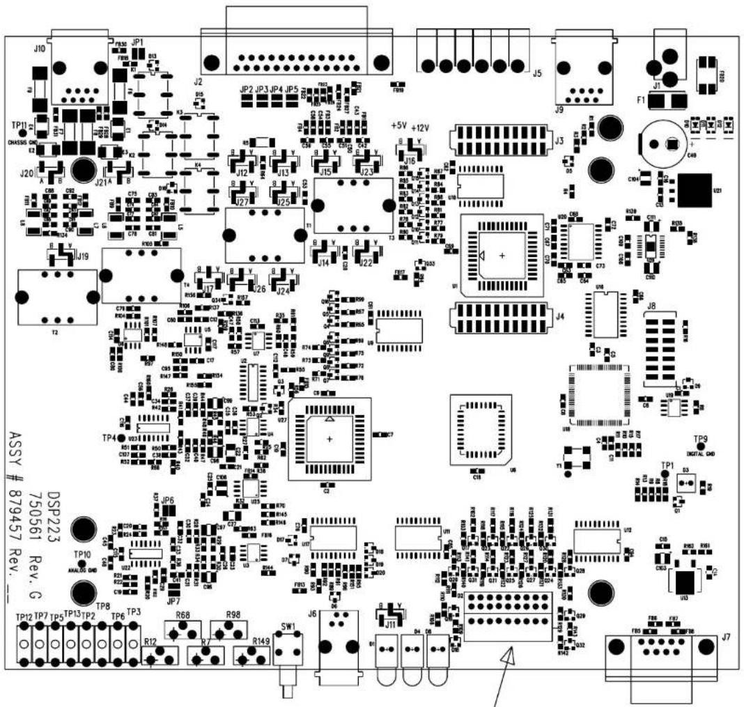

DUAL SEVEN SEGMENT
DISPLAY TO BE INSERTED
INTO SOCKET BEFORE
SOLDERING TO BOARD
BOTTOM OF DISPLAY TO
BE MOUNTED FLUSH WITH
TOP OF BOARD.
REFERENCE SCHEMATIC : 770660
TOP ASSEMBLY
BE, LN


9.4 PCB P/N 750561 Revision H
| This drawing, written description or specification is a proprietary product of TELEX, Lincoln, NE, and shall not be released, disclosed, nor duplicated without the written permission of TELEX. | Telex Communications INC. | PART NO:879457 | |||||
| Lincoln, Nebraska USA | |||||||
| APPROVALS: DR BY: SBCDATE:01/17/2001 | PROD:CHK: APPD: | REV LEVEL: | PQ | ||||
| TITLE: | PCB ASSY, DSP223 MAIN BOARD - BE | ||||||
| REVISIONS | ||||
| REV | DESCRIPTION ECO NO DATE | APPD | ||
| A | RELEASED FOR PILOT BUILD | 01-93-01 | 01/17/01 | SBC |
| B U18 TO 760319 (ADSP-2185M ) | 02-47-01 | 02/20/01 | SBC | |
| C DELETED 7602533PS AND ADDED TO LINCOLN BILL DSP22 3 | 03-39-01 | 03/14/01 | SBC | |
| D R95 NOT TO BE INSTALLED | 04-01-01 | 04/02/01 | sbc | |
| E CHANGE J7 FROM 59926016 TO 64014 9 | 04-47-01 | 04/12/01 | SBC | |
| F ITEM 17 TELEXPN 7602702 CHAGED TO TELEXPN 5868000 C | 04-83-01 | 04/18/01 | SBC | |
| G | ADDED C45,C48,C49, FB20, FB21-FB31 (PCB TO REV D) | 09-23-01 | 09/11/01 | SBC |
| H ITEM 1 - DELETED C28, C32 | 11-93-01 | 11/27/01 | ||
| ITEM 2 - ADDED C28 | ||||
| ITEM 10 - ADED C12,C17 | ||||
| ITEM 38 - DELETED R20 ADDED R63,R95,R96 | ||||
| ITEM 39 - ADDED R106,R136,R137,R147,R148,R150 | ||||
| ITEM 49 - DELETED R37,R63 | ||||
| ITEM 66 - ADDED U5 | ||||
| ITEM 74 - DELETED U24 | ||||
| ADDED ITEM 85 - R20, R37 | ||||
| ADDED ITEM 86 - SCHEMATIC REFERENCE | ||||
| PRINTED CIRCUIT BOARD TO REV E. | ||||
| J | ADDED D18,D19,D20 TO ITEM 19. R95,R96 CHANGED TO 10K | 02-60-02 | 02/12/02 | |
| AND ADDED TO ITEM 39. R151 ADDED TO ITEM 39 | ||||
| R63 TO 267K. C37 TO 1UF AND ADDED TO ITEM 2. | ||||
| ADDED C32,C41,C52 TO ITEM 2. ITEM 1 TO QTY OF 49 | ||||
| ITEM 38 TO QTY OF 11. PCB TO REV F. | ||||
| ON NEXT REV CHANGE THE FOLLOWING | ||||
| item 3 use 102881150 t | ||||
| Item 8 use 102881138 t | ||||
| K R188 FROM 10K TO 1K. ITEM 3 TO 102881150T, ITEM 8 TO 102881138T | 03-50-02 | 03/19/02 | ||
| L ITEM 78 - DELETE 7602673PS - ADD 760519-3P S | 04-20-02 | 04/10/02 | ||
| M REVERSE CHANGE 04-20-0 2 | 05-12-02 | 05/03/02 | ||
| N | ITEM 41 CHANGED TO NEW PART # 724097 | 11-56-02 | 11/25/02 | |
| P | ITEM2 TO QTY OF 10, ITEM 5 TO QTY OF 0, ITEM 10 TO QTY OF 13 | 11-37-02 | 11/25/02 | |
| ITEM 25 CHANGED PART # TO 710109, ITEM 37 QTY TO 34 | ||||
| ITEM 39 QTY TO 79 | ||||
| ITEM 54 TO QTY OF 28, ITEM 68 CHG PART # TO 760250T | ||||
| ADDED ITEM 87 | ||||
| ITEM 38 CHANGED QTY TO 12 | ||||
| ITEM 49 CHANGED QTY TO 5 | ||||
| R | ADDED J17 TO ITEM 34 AND ITEM 80 01-63-0 | 01-62-03 | 1/21/2003 | |
| This drawing, written description or specification is a proprietary product of TELEX, Lincoln, NE, and shall not be released, disclosed, nor duplicated without the written permission of TELEX. | Telex Communications INC. | PART NO:879457 | ||||||
| Lincoln, Nebraska USA | ||||||||
| APPROVALS: | DR BY: SBCDATE: 01/17/2001 | CHKD BY: | APPD BY: | PROD: | REV LEVEL: | Q | ||
| TITLE: | PCB ASSY, DSP223 MAIN BOARD - BE | |||||||
| ITEM | NEW | QTY | TYPE DES | CRIPTION PART NO. DESIGNATOR | ||||
| 1 | 49 | CAPACITOR 0.1UF | 0805 102881186T C1,C2,C3 | C4,C5,C6,C7 | C8,C9,C10,C11, | |||
| C13,C14,C15,C16,C18,C23,C25, | ||||||||
| C35,C44,C60,C61,C62,C66, | ||||||||
| C67,C68,C69,C70,C71,C72,C76,C78,C81, | ||||||||
| C85,C86,C90,C94,C95,C107,C108,C109, | ||||||||
| C112,C113,C114,C115,C116,C117,C45,C48 | ||||||||
| 2 | 10 | CAPACITOR 1UF | 0805 102881875T C19,C20,C26,C36, C28, C32, C37, C41, C52, C53 | |||||
| 3 | 6 | CAPACITOR 0.01UF | 0805 102881150T C21,C24,C77,C82,C87,C91 | |||||
| 4 | 2 | CAPACITOR 0.47UF | 1210 102881445T C22,C27 | |||||
| 5 | CAPACITOR 1800PF | 0805 | ||||||
| 6 | 4 | CAPACITOR 0.018UF | 0805 102881126T C30,C31,C39,C40 | |||||
| 7 | 1 | CAPACITOR 0.047UF | 0805 102881185T C34 | |||||
| 8 | 8 | CAPACITOR 0.001UF | 0805 102881138T C42,C51,C55,C59,C74,C84,C89,C93 | |||||
| 9 | 8 | CAPACITOR 120PF | 0805 102881100T C43,C50 | C54,C58,C75,C83,C88,C92 | ||||
| 10 | 13 | CAPACITOR 220PF | 0805 102881103T | C46,C47,C63,C64,C65,C73,C79,C80,C12,C17,C29C33,C56 | ||||
| 11 | ||||||||
| 12 | 4 | CAPACITOR 3.3UF | TANT. B SIZE 102877021T C96,C97,C98,C99 | |||||
| 13 | 5 | CAPACITOR 10UF | TANT. B SIZE 102877065T | C103,C104,C106,C110,C111 | ||||
| 14 | 1 | LED GREEN RT ANGLE 1610628 D1 | ||||||
| 15 | 1 SOCKET | 18 PIN RT ANGLE 640137 | FOR D2 | |||||
| 16 | 1 | LED DUAL 7 SEGMENT GRN 760309 D2 | ||||||
| 17 | 1 | LED RED LED 58680000 D3 | ||||||
| 18 | 1 | LED RED RT ANGLE 1610630 D4 | ||||||
| 19 | 11 DIODE | MMBD914 SOT-23 58711000T | D5,D6,D7,D13,D14,D15,D16,D17,D18,D19,D20 | |||||
| 20 | 1 | LED YELLOW RT ANGLE 1610631 D8 | ||||||
| 21 | 1 | DIODE MMBZ5V6ALT1 SOT-23 508046000T D9 | ||||||
| 22 | 3 DIODE | SMD4004 16016481SMT | D10,D11,D12 | |||||
| 23 | 4 THYRISTOR | TVB230-050 710106 | E1,E2,E3,E4 | |||||
| 24 | 1 | FUSE 1.5A SMT FUSE 7101051 F1 | ||||||
| 25 | 4 POLYSWITCH | TECCOR F1250T 710109T | F6,F7,F8,F9 | |||||
| 26 | 24 FERRITE | FERRITE BEAD 723511T | FB1,FB2,FB3,FB4,FB5,FB6,FB7,FB8,FB9,FB10,FB11,FB12,FB19, FB21,FB22,FB23,FB24,FB25,FB26,FB27,FB28,FB29,FB30,FB31 | |||||
| 27 | 1 | CONN DC | PWR JACK 2.5MM 59697000 J1 | |||||
| 28 | 1 | CONN 25 PIN DB25 FEMALE 640136 J2 | ||||||
| 29 | 2 | HEADER 20 PIN SMT 640126 J3,J4 | ||||||
| 30 | 1 | HEADER 6 PIN RT ANG LEADED 2862056 J5 | ||||||
| 31 | 1 CONN | RJ-4 PIN CONN LEADED 640123 | J6 | |||||
| 32 | 1 | CONN 9 PIN DB9 FEMALE 640149 J7 | ||||||
| 33 | 2 | CONN 8 PIN MODULAR JACK 2862013 J9,J10 | ||||||
| 34 | 16 HEADER | 3 PIN SMT 640124 | J11,J12,J13,J14,J15,J16,J19,J20,J21,J22,J23,J24,J25,J26,J27,J17 | |||||
| 35 | 4 | RELAY SPDT SMT 730142 K1,K2,K3,K4 | ||||||
| 36 | 4 | INDUCTOR 820UH | 723510 L5,L6,L7,L8 | |||||
| 37 | 34 TRANSISTOR | 2N3904 SOT-23 54671200T Q1,Q2,Q3,Q4,Q5,Q6,Q7,Q8,Q9,Q10,Q11,Q12,Q13,Q14,Q15,Q16,Q17,Q18,Q19,Q20,Q21,Q22,Q23,Q24,Q25,Q26,Q27,Q28,Q29,Q30, | ||||||
| This drawing, written description or specification is a proprietary product of TELEX, Lincoln, NE, and shall not be released, disclosed, nor duplicated without the written permission of TELEX. | Telex Communications INC. | PART NO:879457 | |||||||
| Lincoln, Nebraska USA | |||||||||
| APPROVALS: DR BY: SBCDATE: 01/17/2001 | PROD:CHKD BY: APPD BY: | REV LEVEL: | Q | ||||||
| TITLE:PCB ASSY, DSP223 MAIN BOARD - BE | |||||||||
| ITEM | NEW | QTY | TYPE DES | CRIPTION PART NO. DESIGNATOR | |||||
| Q31,Q32,Q33,Q34 | |||||||||
| 38 | 12 | RESISTOR 0 OHM | 0805 102506000T R1,R2,R3,R105,R139,FB13,FB14,FB15,FB16,FB17 | ||||||
| ,FB18,R154 | |||||||||
| 39 | 79 | RESISTOR 10K 0805 | 102515300T R4,R6,R8,R9,R10,R11,R13 | R14,R15,R16,R17,R18 | |||||
| R21,R22,R23,R33,R34,R41,R42,R43,R48,R49,R50 | |||||||||
| R51,R53,R54,R55,R56,R65,R67,R69,R72,R75, | |||||||||
| R76,R77,R79,R81,R84,R87,R88,R89,R90 | |||||||||
| R91,R92,R93,R94,R99,R103,R108,R110,R112, | |||||||||
| R115,R118,R119,R121,R122,R124,R126 | |||||||||
| R129,R132,R133,R135,R140,R142, | |||||||||
| R106,R136,R137,R147,R148,R150,R95,R96,R151 | |||||||||
| R152,R153,R156,R157,R159,R160 | |||||||||
| 40 | 1 | RESISTOR 10 OHMS | 2010 102405100T R5 | ||||||
| 41 | 5 | RES VAR 100K LINEAR H.ADJUST 724097 | R7,R12,R68,R98,R149 | ||||||
| 42 | 1 | RESISTOR 30K 0805 | 102515346T R24 | ||||||
| 43 | 7 | RESISTOR 47 OHMS | 0805 102515065T R25,R38,R62,R70,R144,R145,R146 | ||||||
| 44 | 4 | RESISTOR 20K 0805 | 102515329T R26,R36,R39,R52 | ||||||
| 45 | 3 | RESISTOR 150 OHMS | 0805 1025151 | 17T R27,R32,R61 | |||||
| 46 | 4 | RESISTOR 562 OHMS | 0805 1025151 | 72T R28,R31,R44,R47 | |||||
| 47 | 5 | RESISTOR 267K 0805 | 1025154 | 41T R29,R30,R45,R46,R63 | |||||
| 48 | 1 | RESISTOR 15 OHMS | 0805 102515017T R35 | ||||||
| 49 | 5 | RESISTOR 33K 0805 | 102515350T R59,R60,R101,R104,R155 | ||||||
| 50 | 1 | RESISTOR 332 OHMS | 0805 1025151 | 50T R40 | |||||
| 51 | 4 | RESISTOR 100K 0805 | 1025154 | 00T R57,R58,R97,R100 | |||||
| 52 | 2 | RESISTOR 604 OHMS | 0805 1025151 | 75T R64,R134 | |||||
| 53 | 1 | RESISTOR 681 OHMS | 0805 1025151 | 80T R66 | |||||
| 54 | 28 | RESISTOR 1K 0805 | 102515200 | R19,R71,R73,R74,R78,R80,R82,R83,R85,R86, | |||||
| R102,R109,R111,R113,R114,R116,R117, | |||||||||
| R120,R123,R125,R127,R128,R130,R131, | |||||||||
| R141,R143, R138, R162 | |||||||||
| 55 | |||||||||
| 56 | 1 | RESISTOR 301 OHMS | 0805 1025151 | 46T R107 | |||||
| 57 | 1 SWITCH | PUSH BUTTON SPST | 57502000 | SW1 | |||||
| 58 | 2 | TRANSFER 10K-10K THRU-HOLE 3180246 T1,T2 | |||||||
| 59 | 2 | TRANSFER 600-600 THRU-HOLE 3180259 T3,T4 | |||||||
| 60 | 8 | TEST JACK ORANGE 2861965 TP2,TP3,TP5,TP6,TP7,TP8,TP12,TP13 | |||||||
| 61 | 1 | IC TL16C550CFN 760262 U1 | |||||||
| 62 | 1 | IC 4053 SO16 53266123 U2 | |||||||
| 63 | 2 | IC CS4335 SO8 760263 U3,U4 | |||||||
| 64 | 1 | SOCKET PLCC 32 PIN PLCC SOCKET 539030032T U6 SOCKET | |||||||
| 65 | |||||||||
| 66 | 3 | IC NE5532 SO8 760268 U7,U8,U5 | |||||||
| 67 | 4 IC 74LCX574 SO20 760257 U9,U10,U11,U12 | ||||||||
| 68 | 1 | IC LM317M 760250T U13 | |||||||
| 69 | 2 | IC 74LCX541 SO20 760256 U16,U17 | |||||||
| 70 | 1 | IC AD$P-2186M TQFP100 760319 U18 | |||||||
| 71 | 1 | IC AT24C16N SO8 511336000T U19 | |||||||
| 72 | 1 | IC LT1181ACSW 760261 U20 | |||||||
| This drawing, written description or specification is a proprietary product of TELEX, Lincoln, NE, and shall not be released, disclosed, nor duplicated without the written permission of TELEX. | Telex Communications INC. | PART NO:879457 | ||||||||
| Lincoln, Nebraska USA | ||||||||||
| APPROVALS: DR BY: SBCDATE: 01/17/2001 | PROD:CHKD BY: APPD BY: | REV LEVEL: | Q | |||||||
| TITLE: | PCB ASSY, DSP223 MAIN BOARD - BE | |||||||||
| ITEM | NEW | QTY | TYPE DES | CRIPTION PART NO. DESIGNATOR | ||||||
| 73 | 1 | IC | UA7805CKTE SM | T 760260T U21 | ||||||
| 74 | 2 | IC | TL084 SO14 4300 | 0047 U22,U23 | ||||||
| 75 | 1 | IC | CS5330A SO8WB | 760264 U25 | ||||||
| 76 | 1 | IC | TPS70158 76030 | 6 U26 | ||||||
| 77 | 1 | SO | CKET PLCC 44 PIN PLCC SOCKET | 5390 | 30044 U27 | SOCKET | ||||
| 78 | 1 | IC | EPM7032AE PLC | C44 760267-3PS U27 (PROGRAMMED) | ||||||
| 79 | 1 | 32.768MHZ | 780 | 186 Y1 | ||||||
| 80 | 16 | JUMPER | JUMPER | 2515001001 | FOR J11,J12,J13,J14,J15,J16,J19,J20,J21,J22,J23,J24,J25,J26,J27,J17 | |||||
| 81 | 1 | PCB | PRINTED CIRCUIT BOAR D | 750561 | ||||||
| 82 | A/R | SOLDER PASTE | BE738 | |||||||
| 83 | 1 | CAP | 1000UF ELECT H SIZE | 51821526 | C49 | |||||
| 84 | 1 | FERRITE | COMMON MODE | 724039 | FB20 | |||||
| 85 | 2 | RES | 8.06K 0805 | 102515287 | R20, R37 | |||||
| 86 | 0 | REFERENCE | SCHEMATIC | 770660 | ||||||
| 87 | 1 | RES | 6.98K 0805 | 102515281T | R161 | |||||
| This drawing, written description or specification is a proprietary product of Telex, Lincoln, NE and shall not be released, disclosed, nor duplicated without the written permission of TELEX | Telex Communications Inc. | PART NO:879457 | ||||
| Lincoln, Nebraska USA | ||||||
| APPROVALS | DR BY: SBCDATE: 01/17/2001 | CHK: | APPD: | PROD: | REV LEVEL: | RQ |
| TITLE | PCB ASSY, DSP223 MAIN BOARD - BE | |||||
750561 REV H
SORSOREEN TOP


DUAL SEVEN SEGMENT
DISPLAY TO BE INSERTED
INTO SOCKET BEFORE
SOLDERING TO BOARD
BOTTOM OF DISPLAY TO
BE MOUNTED FLUSH WITH
TOP OF BOARD.
REFERENCE SCHEMATIC : 770660
TOP ASSEMBLY
BE, LN
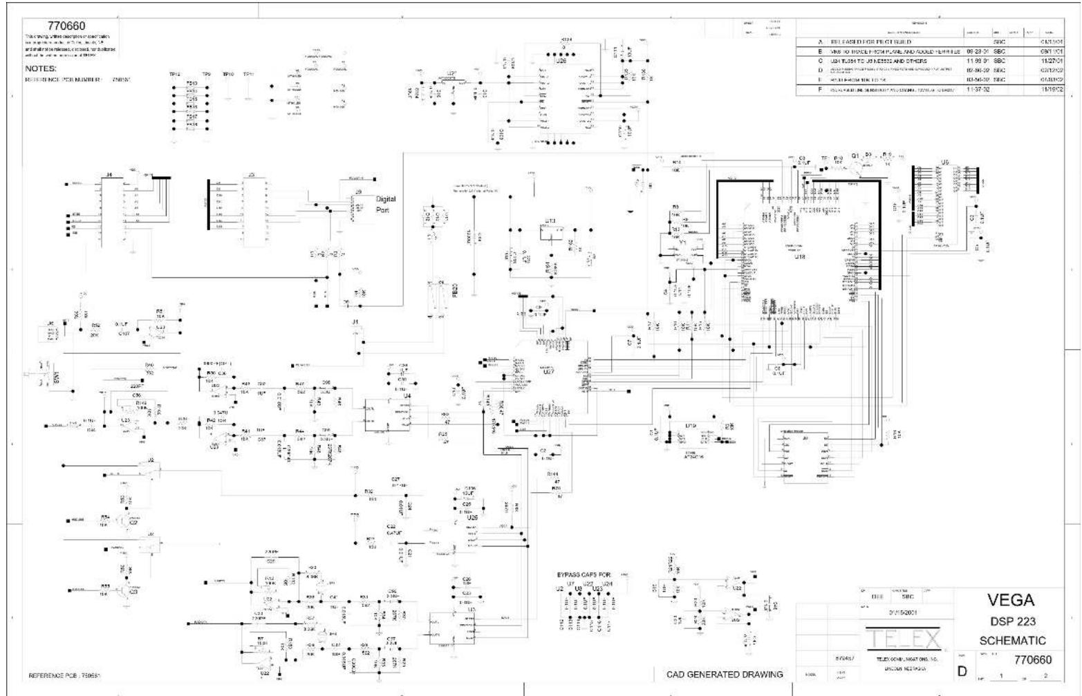

10 Warranty, Service, Repair, and Comments
Important! Be sure the exact return address and a description of the problem or work to be done are enclosed with your equipment.
Warranty (Limited)
All Telex Communications, Inc. manufactured Vega Signaling products are guaranteed against malfunction due to defects in materials and workmanship for three years, beginning at the date of original purchase. If such a malfunction occurs, the product will be repaired or replaced (at our option) without charge during the three-year period, if delivered to the Telex factory. Warranty does not extend to damage due to improper repairs, finish or appearance items, or malfunction due to abuse or operation under other than the specified conditions, nor does it extend to incidental or consequential damages. Some states do not allow the exclusion or limitation of incidental or consequential damages, so the above limitation may not apply to you. This warranty gives the customer specific legal rights, and there may be other rights which vary from state to state.
Factory Service Center
TELEX Communications, Inc.
Vega Signaling Products
8601 East Cornhusker Highway, Lincoln, Nebraska, 68507
Phone: (402) 465-7026 / (800) 752-7560 Fax: (402) 467-3279
E-mail: vega@telex.com Web: www.vega-signaling.com
Claims
No liability will be accepted for damages directly or indirectly arising from the use of our materials or from any other causes. Our liability shall be expressly limited to replacement or repair of defective materials.
Suggestions or Comments
We'd appreciate your input. Please send us your suggestions or comments concerning this manual, by fax (402-467-3279) or e-mail them to: vega@telex.com
Visit our web site at www.vega-signaling.com
11 DSP-223 Specifications
Operating Temperature Range: 0 to 70°C for full specifications
Power Requirements: +12 to +16 Vdc, semi-regulated, 500ma.
Relay Contact Ratings: 1A at 125Vac
Radio Interface: ±45 Vdc withstand rating
Line to TX Output Gain: -10dB to +25dB, user settable
Radio Output Level: 10mVp-p to 9Vp-p for microphone level or -40 to +10dBm into 600Ω load, adjustable
Radio Output Impedance: 600Ω for balanced mode, 200Ω for single ended mode
Radio Input Level: 100mVrms to 16Vrms, adjustable
Audio Distortion: 2% THD maximum
Frequency Response: ±1.5 dB, 300 to 3000 Hz, except at 2175 Hz notch frequency
Line Output Level: -40 to +10dBm, adjustable
Line Input/Output Impedance: 600Ω nominal, or 10kΩ receive
Sensitivity: Ultimate sensitivity, -25dBm PTT tone
Frequency-Select Function Tone Decoder Tuning Range: Not tunable by field personnel, only by software change
Function-Tone Detection Bandwidth: ±20 Hz around center of frequency
DTMF Detection Bandwidth: ± 25 Hz around center of frequency
MON timer: 10ms to 65seconds, adjustable
PTT Detect Frequencies: Programmable 2100, 2155, 2175, 2300, 2325, 2600, 2800 and 2970Hz
PTT Tone Detect Bandwidth: ± 20 Hz
Tone-Detect Stability: 100 ppm
Notch Frequency Bandwidth: 50 Hz at -3dB points. ±1Hz at -40dB.
Notch Frequency Rejection: 45 dB minimum
Morse Code Transmitter: 20 wpm, 400-2000Hz carrier selectable, 50 chars max, -40 to 0 dB or range relative to max radio level output.
Voter Status: Programmable active Hi/Low, 0 to -20dbm, 300 to 3000Hz
Radio Interface: ± 45 Vdc withstand rating
Non-Relay Outputs: Open collector, active low, 200mA maximum, 40V collector to emitter voltage
Dimensions: 8 ½" Wide, 7 1/8" Deep, by 1 5/8" High
Specifications are subject to change without notice
TELEX Communications, Inc.
Vega Signaling Products
8601 East Cornhusker Highway, Lincoln, Nebraska, 68507
Phone: (402) 465-7026 / (800) 752-7560 Fax: (402) 467-3279
E-mail: vega@telex.com, Web: www.vega-signaling.com
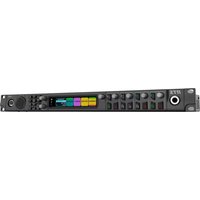

- Technical Manual
- Table of Contents
- General.... 1
- Installation 2
- Level Settings....5
- Programming and Operation 7
- Theory of Operation....19
- Loading the DSP-223 Operational Software 20
- Specific Radio Control.... 20
- Pin out and Jumper Settings Quick Reference Table...... 21
- Schematics and Parts Lists 22
- Warranty, Service, Repair, and Comments.... 26
- DSP-223 Specifications 27
- Table of Figures
- General
- Unless noted, this manual refers to DSP-223 operating software 2.6.
- The DSP-223 provides the following features:
- DSP-223 Accessories
- Installation
- DSP-223 Power Supply
- DSP-223 to Console Line Connection
- DSP-223 to Radio Connection
- TX Audio Connection
- RX Audio Connection
- PTT Connection
- Monitor Connection
- Radio Frequency Control
- CTCSS Connection
- Handset Connection
- Digital Expansion Port
- Level Settings
- Line Receive Level Adjust Procedure
- Revision G PCB's with J17
- Radio TX Level Adjust Procedure
- Radio RX Level Adjust Procedure
- Line TX Level Adjust Procedure
- CTCSS Level (Continuous Tone coded Squelch)
- DSP-223 Detection Frequencies
- Programming and Operation
- Software Installation
- Windows® Application Software Operation
- Select a Serial Port
- DSP-223 Configuration
- Function Tone Mode
- CTCSS Tone
- PTT Options
- Monitor Relay Options
- EE/Error Beeps (Rev 2.0 or higher)
- Line DTMF Decoder
- Audio Loop Back
- Individual Function Tone Setup
- Tone Active
- Relay
- Relay Group
- Relay Duration
- Digital Output
- CTCSS Frequency and Default
- DIG4 Setup Button
- DIG5 Setup Button
- Voter/Ring Down Tone Generation
- Set Gains Button
- Morse Code Station Identifier Setup
- Save and Load Buttons
- Send and Receive Configuration from DSP-223
- Radio TX Audio Filters
- AGC
- Add CTCSS to TX
- Pre-Emphasize Audio
- 3.5kHz Low Pass Filter
- DSP-223 Audio Block Diagram
- DSP-223 Frequency Response
- DTMF Responder Functions
- \*0#1 : Increase Radio TX Gain
- \*0#2 : Decrease Radio TX Gain
- \*0#3 : Increase Line TX Gain
- \*0#4 : Decrease Line TX Gain
- \*0#5 : Increase CTCSS Gain
- \*0#6 : Decrease CTCSS Gain
- \*0#7 : Loopback Line RX to Line TX
- \*0#8 : Send 1kHz Tone to both Radio and Line Interfaces
- \*0#9 : Toggle SCAN Mode of the Kenwood x150/x180 Radio
- \*0#10 : Send the last Kenwood FleetSync® ANI data
- Theory of Operation
- DSP-223 Audio Input Paths
- DSP-223 Audio Output Paths
- Troubleshooting Aid
- Loading the DSP-223 Operational Software
- Specific Radio Control
- PCB P/N 750561 Revision G
- PCB P/N 750561 Revision H
- Warranty, Service, Repair, and Comments
- Warranty (Limited)
- Factory Service Center
- TELEX Communications, Inc.
- Claims
- Suggestions or Comments
- DSP-223 Specifications
Brand : Telex
Model : DSP-223
Category : Radio