
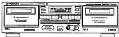
CT-05D - Cassette player PIONEER - Free user manual and instructions
Find the device manual for free CT-05D PIONEER in PDF.

User questions about CT-05D PIONEER
0 question about this device. Answer the ones you know or ask your own.
Ask a new question about this device
Download the instructions for your Cassette player in PDF format for free! Find your manual CT-05D - PIONEER and take your electronic device back in hand. On this page are published all the documents necessary for the use of your device. CT-05D by PIONEER.
USER MANUAL CT-05D PIONEER
PIONEER®
The Art of Entertainment
• The above illustration shows CT-W706DR.
ORDER NO. RRV1784
STEREO DOUBLE CASSETTE DECK
CT-W706DR
CT-W606DR
CT-05D
THIS MANUAL IS APPLICABLE TO THE FOLLOWING MODEL(S) AND TYPE(S).
| Type | Model | Power requirement | Remarks | ||
| CT-W706DR | CT-W606DR | CT-05D | |||
| HYXJ | ○ | ○ | — | AC 220-230V | —— |
| HVXJ | — | ○ | — | AC 230-240V | —— |
| HPWXJ | — | ○ | — | AC 230-240V | —— |
| SDXJ | ○ | ○ | — | AC 110/120-127/220/230-240V | With the voltage selector |
| SLXJ | — | ○ | — | AC 110/120-127/220/230-240V | With the voltage selector |
| KUXJ/CA | — | — | ○ | AC 120V | —— |
CONTENTS
- SAFETY INFORMATION ...... 2
- EXPLODED VIEWS AND PARTS LIST .... 3
- SCHEMATIC DIAGRAM 12
- PCB CONNECTION DIAGRAM 22
- PCB PARTS LIST 28
-
ADJUSTMENT 31
-
GENERAL INFORMATION 35
7.1 PARTS 35
7.1.1 IC 35
7.1.2 DISPLAY 39
7.2 TEST MODE 40
7.3 BLOCK DIAGRAM 43
- PANEL FACILITIES AND SPECIFICATIONS ... 44
1. SAFETY INFORMATION
This service manual is intended for qualified service technicians; it is not meant for the casual do-it-yourselfer. Qualified technicians have the necessary test equipment and tools, and have been trained to properly and safety repair complex products such as those covered by this manual.
Improperly performed repairs can adversely affect the safety and reliability of the product and may void the warranty. If you are not qualified to perform the repair of this product properly and safety, you should not risk trying to do so and refer the repair to a qualified service technician.
WARNING
Lead in solder used in this product is listed by the California Health and Welfare agency as a known reproductive toxicant which may cause birth defects or other reproductive harm (California Health & Safety Code, Section 25249.5).
When servicing or handling circuit boards and other components which contain lead in solder, avoid unprotected skin contact with the solder. Also, when soldering do not inhale any smoke or fumes produced.
NOTICE
(FOR CANADIAN MODEL ONLY)
Fuse symbols - (fast operating fuse) and/or - (slow operating fuse) on PCB indicate that replacement parts must be of identical designation.
REMARQUE
(POUR MODÈLE CANADIEN SEULEMENT)
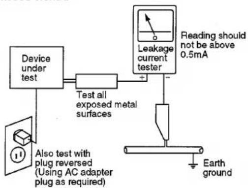
The following check should be performed for the continued protection of the customer and service technician.
LEAKAGE CURRENT CHECK
Measure leakage current to a known earth ground (water pipe, conduit, etc.) by connecting a leakage current tester such as Simpson Model 229-2 or equivalent between the earth ground and all exposed metal parts of the appliance (input/output terminals, screwheads, metal overlays, control shaft, etc.). Plug the AC line cord of the appliance directly into a 120V AC 60Hz outlet and turn the AC power switch on. Any current measured must not exceed 0.5mA.
flowchart
graph TD
    A["Device under test"] --> B["Test all exposed metal surfaces"]
    B --> C["Leakage current tester"]
    C --> D["Reading should not be above 0.5mA"]
    E["Also test with plug reversed (Using AC adapter plug as required)"] --> B
    F["Earth ground"] --> C
AC Leakage Test
ANY MEASUREMENTS NOT WITHIN THE LIMITS OUTLINED ABOVE ARE INDICATIVE OF A POTENTIAL SHOCK HAZARD AND MUST BE CORRECTED BEFORE RETURNING THE APPLIANCE TO THE CUSTOMER.
2. PRODUCT SAFETY NOTICE
Many electrical and mechanical parts in the appliance have special safety related characteristics. These are often not evident from visual inspection nor the protection afforded by them necessarily can be obtained by using replacement components rated for voltage, wattage, etc. Replacement parts which have these special safety characteristics are identified in this Service Manual.
Electrical components having such features are identified by marking with a △ on the schematics and on the parts list in this Service Manual.
The use of a substitute replacement component which dose not have the same safety characteristics as the PIONEER recommended replacement one, shown in the parts list in this Service Manual, may create shock, fire, or other hazards.
Product Safety is continuously under review and new instructions are issued from time to time. For the latest information, always consult the current PIONEER Service Manual. A subscription to, or additional copies of, PIONEER Service Manual may be obtained at a nominal charge from PIONEER.
2. EXPLODED VIEWS AND PARTS LIST
NOTES: • Parts marked by "NSP" are generally unavailable because they are not in our Master Spare Parts List.
- The mark found on some component parts indicates the importance of the safety factor of the part.
Therefore, when replacing, be sure to use parts of identical designation.
- Screws adjacent to ▼ mark on the product are used for disassembly.
2.1 PACKING
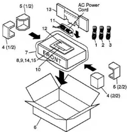
(1) PARTS LIST
| Mark | No. | Description | Part No. |
| 1 | Connection Cord with Pin Plug (L=0.9 m) | RDE1036 | |
| 2 | Remote Control Cord (L=1.0 m) | PDE1267 | |
| 3 | CD•Deck Synchro Control Cord (L=0.9 m) | RDE1044 | |
| 4 | Pad F | RHA1219 | |
| 5 | Pad R | RHA1236 | |
| 6 | Packing Case | See Contrast table (2) | |
| 7 | Seat (750×600×0.5) | Z23-007 | |
| 8 | Operating Instructions (German/Italian/Dutch/Swedish/Spanish/Portuguese) | See Contrast table (2) | |
| 9 | Operating Instructions (English/French) | See Contrast table (2) | |
| NSP | 10 | Warranty Card | See Contrast table (2) |
| 11 | Vinyl Bag | See Contrast table (2) | |
| 12 | Caution 220V Label | See Contrast table (2) | |
| 13 | Spacer | See Contrast table (2) | |
| 14 | Operating Instructions (English/Spanish/Chinese) | See Contrast table (2) | |
| 15 | Operating Instructions (English) | See Contrast table (2) |
(2) CONTRAST TABLE
● For CT-W706DR and CT-05D
CT-W706DR/HYXJ,SDXJ and CT-05D/KUXJ/CA have the same construction except for the following :
| Mark | No. | Symbol and Description | Part No. | Remarks | ||
| CT-W706DR | CT-05D | |||||
| HYXJ | SDXJ | KUXJ/CA | ||||
| NSP | 6 | Packing Case | RHG1807 | RHG1825 | RHG1808 | |
| 8 | Operating Instructions(German/Italian/Dutch/Swedish/Spanish/Portuguese) | RRD1190 | Not used | Not used | ||
| 9 | Operating Instructions (English/French) | RRE1148 | Not used | RRE1150 | ||
| 10 | Warranty Card | ARY7009 | Not used | ARY7007 | ||
| 11 | Vinyl Bag | Not used | Not used | Not used | ||
| 12 | Caution 220V Label | Not used | ARR1003 | Not used | ||
| 13 | Spacer | Not used | Not used | Not used | ||
| 14 | Operating Instructions (English/Spanish/Chinese) | Not used | RRE1153 | Not used | ||
| 15 | Operating Instructions (English) | Not used | Not used | Not used | ||
● For CT-W606DR
CT-W606DR/HYXJ,HVXJ,HPWXJ,SDXJ and SLXJ have the same construction except for the following :
| Mark | No. | Symbol and Description | Part No. | Remarks | |||
| CT-W606DR | |||||||
| HYXJ | HVXJ | HPWXJ | SDXJ, SLXJ | ||||
| NSP | 6 | Packing Case | RHG1803 | RHG1826 | RHG1802 | RHG1801 | |
| 8 | Operating Instructions (German/Italian/Dutch/Swedish/Spanish/Portuguese) | RRD1190 | Not used | Not used | Not used | ||
| 9 | Operating Instructions (English/French) | RRE1148 | Not used | Not used | Not used | ||
| 10 | Warranty Card | ARY7009 | ARY7009 | PRY1003 | Not used | ||
| 11 | Vinyl Bag | Not used | Z21-013 | Not used | Not used | ||
| 12 | Caution 220V Label | Not used | Not used | Not used | ARR1003 | ||
| 13 | Spacer | Not used | RHC1071 | RHC1071 | Not used | ||
| 14 | Operating Instructions (English/Spanish/Chinese) | Not used | Not used | Not used | RRE1153 | ||
| 15 | Operating Instructions (English) | Not used | RRB1176 | RRB1176 | Not used | ||
CT-W706DR, CT-W606DR, CT-05D
2.2 EXTERIOR
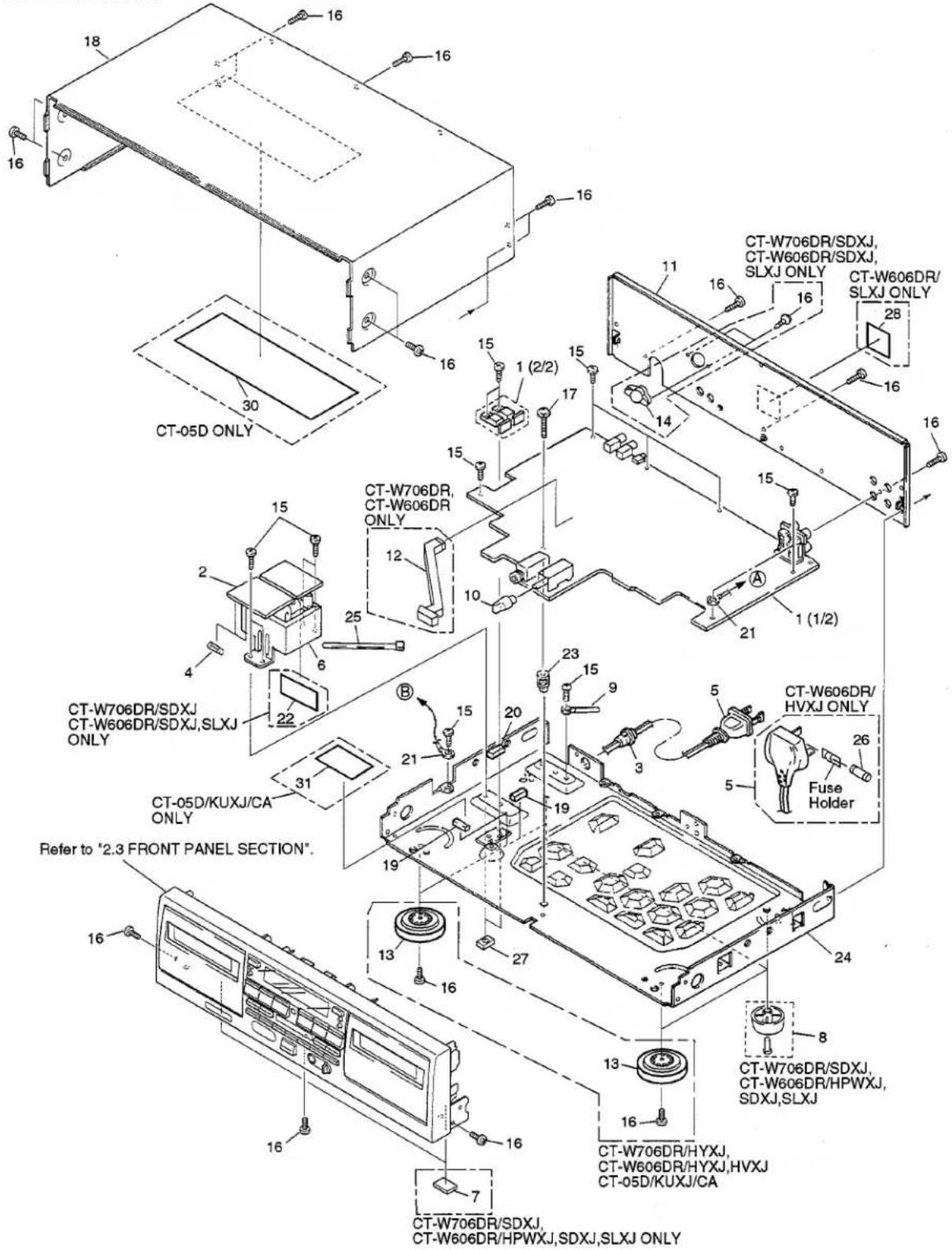
(1) PARTS LIST
| Mark | No. | Description | Part No. |
| 1 | MAIN Unit | See Contrast table (2) | |
| NSP | 2 | TRANS Unit | See Contrast table (2) |
| 3 | Strain Relief | See Contrast table (2) | |
| 4 | Fuse (FU1001, FU1002) | See Contrast table (2) | |
| 5 | AC Power Cord | See Contrast table (2) | |
| 6 | Power Transformer | See Contrast table (2) | |
| 7 | Sheet Rubber | See Contrast table (2) | |
| 8 | Foot Assy | See Contrast table (2) | |
| 9 | Cord Holder | RNH-184 | |
| 10 | Rotary Knob | See Contrast table (2) | |
| 11 | Rear Panel | See Contrast table (2) | |
| 12 | Power Button P | See Contrast table (2) | |
| 13 | Insulator | See Contrast table (2) | |
| 14 | Voltage Selector | See Contrast table (2) | |
| 15 | Screw | BBZ30P060FMC |
| Mark | No. | Description | Part No. |
| NSP | 16 | Screw | BBZ30P080FZK |
| 17 | Screw | IBZ30P150FCC | |
| 18 | Bonnet | REA1254 | |
| 19 | Spacer (CR) | REB1267 | |
| 20 | Spacer | REB1171 | |
| NSP | 21 | Earth Lead Wire | DE010VFO |
| NSP | 22 | Plate | See Contrast table (2) |
| NSP | 23 | PCB Spacer | PNY-404 |
| NSP | 24 | Main Chassis | RNB1091 |
| NSP | 25 | Binder | ZCA-T18S |
| 26 | Fuse (T5A)(For AC Power Cord) | See Contrast table (2) | |
| NSP | 27 | Disc Guard | REC1305 |
| 28 | SISIR Registration | See Contrast table (2) | |
| 29 | ······ | ||
| NSP | 30 | 65 Label | See Contrast table (2) |
| 31 | Fuse Caution Label | See Contrast table (2) |
(2) CONTRAST TABLE
● For CT-W706DR and CT-05D
CT-W706DR/HYXJ,SDXJ and CT-05D/KUXJ/CA have the same construction except for the following :
| Mark | No. | Symbol and Description | Part No. | Remarks | ||
| CT-W706DR | CT-05D | |||||
| HYXJ | SDXJ | KUXJ/CA | ||||
| 1 | MAIN Unit | RWZ4108 | RWZ4111 | RWZ4125 | ||
| NSP | 2 | TRANS Unit | RWZ4105 | RWZ4112 | RWZ4115 | |
| 3 | Strain Relief | CM-22B | CM-22B | CM-22C | ||
| 4 | Fuse (T1.6AL250V, FU1001,FU1002) | REK1024 | REK1024 | Not used | ||
| 4 | Fuse (1.5A/250V, FU1001,FU1002) | Not used | Not used | REK1059 | ||
| 5 | AC Power Cord | PDG1058 | ADG1157 | PDG1015 | ||
| 6 | Power Transformer | RTT1334 | RTT1335 | RTT1333 | ||
| 7 | Sheet Rubber | Not used | AEB1111 | Not used | ||
| 8 | Foot Assy | Not used | AEC1531 | Not used | ||
| 10 | Rotary Knob | RAC1903 | RAC1903 | Not used | ||
| 10 | Headphone Knob | Not used | Not used | VNK1262 | ||
| 11 | Rear Panel | RNA2152 | RNA2166 | RNA2153 | ||
| 12 | Power Button P | RAC2156 | RAC2156 | Not used | ||
| 13 | Insulator | PNW1912 | Not used | PNW1912 | ||
| 14 | Voltage Selector (AC110V/120-127V/220V/230-240V) | Not used | RSB1022 | Not used | ||
| NSP | 22 | Plate | Not used | DEC1158 | Not used | |
| 30 | 65 Label | Not used | Not used | ORW1069 | ||
| NSP | 31 | Fuse Caution Label | Not used | Not used | RRW-111 | |
● For CT-W606DR
CT-W606DR/HYXJ,HVXJ,HPWXJ,SDXJ and SLXJ have the same construction except for the following :
| Mark | No. | Symbol and Description | Part No. | Remarks | ||||
| CT-W606DR | ||||||||
| HYXJ | HVXJ | HPWXJ | SDXJ | SLXJ | ||||
| 1 | MAIN Unit | RWZ4113 | RWZ4113 | RWZ4113 | RWZ4117 | RWZ4117 | ||
| NSP | 2 | TRANS Unit | RWZ4105 | RWZ4105 | RWZ4105 | RWZ4112 | RWZ4112 | |
| 3 | Strain Relief | CM-22B | CM-22B | CM-22B | CM-22B | CM-22B | ||
| 4 | Fuse (T1.6AL250V, FU1001, FU1002) | REK1024 | REK1024 | REK1024 | REK1024 | REK1024 | ||
| 4 | Fuse (1.5A/250V, FU1001, FU1002) | Not used | Not used | Not used | Not used | Not used | ||
| 5 | AC Power Cord | PDG1058 | PDG1055 | ADG1159 | ADG1157 | PDG1058 | ||
| 6 | Power Transformer | RTT1334 | RTT1334 | RTT1334 | RTT1335 | RTT1335 | ||
| 7 | Sheet Rubber | Not used | Not used | AEB1111 | AEB1111 | AEB1111 | ||
| 8 | Foot Assy | Not used | Not used | AEC1531 | AEC1531 | AEC1531 | ||
| 10 | Rotary Knob | RAC1903 | RAC1903 | RAC1903 | RAC1903 | RAC1903 | ||
| 10 | Headphone Knob | Not used | Not used | Not used | Not used | Not used | ||
| 11 | Rear Panel | RNA2148 | RNA2167 | RNA2147 | RNA2145 | RNA2146 | ||
| 12 | Power Button P | RAC2156 | RAC2156 | RAC2156 | RAC2156 | RAC2156 | ||
| 13 | Insulator | PNW1912 | PNW1912 | Not used | Not used | Not used | ||
| 14 | Voltage Selector (AC110V/120-127V/220V/230-240V) | Not used | Not used | Not used | RSB1022 | RSB1022 | ||
| NSP | 22 | Plate | Not used | Not used | Not used | DEC1158 | DEC1158 | |
| 26 | Fuse (T5A) (For AC Power Cord) | Not used | PEK1003 | Not used | Not used | Not used | ||
| NSP | 28 | SISIR Registration | Not used | Not used | Not used | Not used | RRW1283 | |
| 30 | 65 Label | Not used | Not used | Not used | Not used | Not used | ||
2.3 FRONT PANEL SECTION
(1) PARTS LIST for CT-W706DR
| Mark | No. | Description | Part No. | Mark | No. | Description | Part No. |
| 1 | SUBB Unit | RWZ4109 | 29 | ······ | |||
| 2 | Joint Arm | RNK2243 | 30 | Indicator Lens | RAC2157 | ||
| 3 | Lead Card 33P | RDD1372 | 31 | Screw | BBZ30P080FZK | ||
| 4 | 1 Mechanism Unit (P) | RYM1261 | 32 | Function Button C | RAC2154 | ||
| 5 | 2 Mechanism Unit (R/P) | RYM1262 | 33 | ······ | |||
| 6 | ······ | 34 | ······ | ||||
| 7 | ······ | 35 | Eject Button | REA1267 | |||
| 8 | ······ | NSP | 36 | Earth Lead Wire | DE010VFO | ||
| 9 | Half Pressure Spring | RBK1004 | 37 | Connector Assy 3P | RKP1678 | ||
| 10 | ······ | 38 | Connector Assy 5P | RKP1677 | |||
| 11 | ······ | 39 | ······ | ||||
| 12 | ······ | 40 | ······ | ||||
| 13 | ······ | 41 | Loading Base Assy 1 | RXA1741 | |||
| 14 | ······ | 42 | Loading Base Assy 2 | RXA1750 | |||
| 15 | ······ | 43 | Screw | BBZ30P100FMC | |||
| 16 | ······ | NSP | 44 | EJECT 1 Unit | RWZ4123 | ||
| 17 | ······ | NSP | 45 | EJECT 2 Unit | RWZ4124 | ||
| 18 | ······ | 46 | DC Motor / 0.75W | PXM1010 | |||
| 19 | Function Button A | RAC2172 | 47 | Rubber Belt | PEB1127 | ||
| 20 | Function Button B | RAC2173 | 48 | Motor Pulley | PNW1634 | ||
| 21 | FL Lens | See Contrast table (2) | 49 | Pulley Gear | RNK1517 | ||
| 22 | Front Panel | See Contrast table (2) | 50 | Arm Gear | RNK2242 | ||
| 23 | Door Pocket L | RAH2792 | NSP | 51 | MOTOR 1 Unit | RWZ4191 | |
| 24 | Door Pocket R | RAH2793 | NSP | 52 | MOTOR 2 Unit | RWZ4192 | |
| 25 | Door Lens | RAH2782 | 53 | ······ | |||
| 26 | Name Plate | PAM1608 | 54 | Screw | IPZ20P080FMC | ||
| 27 | Remain Display Paper | REE-113 | 55 | Screw | BMZ26P040FMC | ||
| 28 | ······ | 56 | Screw | BBZ26P060FMC |
(2) CONTRAST TABLE for CT-W706DR
CT-W706DR/HYXJ and SDXJ have the same construction except for the following :
| Mark | No. | Symbol and Description | Part No. | Remarks | |
| CT-W706DR | |||||
| HYXJ | SDXJ | ||||
| 21 | FL Lens | RAH2810 | RAH2809 | ||
| 22 | Front Panel | RAH2800 | RAH2828 | ||
CT-W706DR, CT-W606DR, CT-05D
(3) PARTS LIST for CT-W606DR and CT-05D
| Mark | No. | Description | Part No. | Mark | No. | Description | Part No. |
| 1 | SUBB Unit | See Contrast table (4) | 29 | Eject Lever R | RNK2247 | ||
| 2 | ••••• | 30 | Indicator Lens | RAC2157 | |||
| 3 | Lead Card 33P | RDD1372 | 31 | Screw | BBZ30P080FZK | ||
| 4 | 1 Mechanism Unit (P) | RYM1261 | 32 | Function Button C | RAC2154 | ||
| 5 | 2 Mechanism Unit (R/P) | RYM1262 | 33 | Cushion | See Contrast table (4) | ||
| 6 | Door Spring L | RBH1304 | 34 | Sealing Panel | See Contrast table (4) | ||
| 7 | Door Spring R | RBH1305 | 35 | Eject Button | RAC2158 | ||
| 8 | Eject Spring L | RBH1441 | NSP | 36 | Earth Lead Wire | DE010VFO | |
| 9 | Half Pressure Spring | RBK1004 | 37 | Connector Assy 3P | RKP1678 | ||
| 10 | Eject Spring R | RBH1442 | 38 | Connector Assy 5P | RKP1677 | ||
| 11 | ••••• | 39 | Cushion | See Contrast table (4) | |||
| 12 | Damper Assy | REC1267 | 40 | Sealing Spring | See Contrast table (4) | ||
| 13 | Eject Collar | RLA1283 | 41 | ••••• | |||
| 14 | Arm Collar | RLA1290 | 42 | ••••• | |||
| 15 | Eject Arm | RNE1909 | 43 | ••••• | |||
| 16 | Screw | BCZ26P050FMC | 44 | ••••• | |||
| 17 | Screw | BSZ26P120FMC | 45 | ••••• | |||
| 18 | Power Button | See Contrast table (4) | 46 | ••••• | |||
| 19 | Function Button A | RAC2172 | 47 | ••••• | |||
| 20 | Function Button B | RAC2173 | 48 | ••••• | |||
| 21 | FL Lens | See Contrast table (4) | 49 | ••••• | |||
| 22 | Front Panel | See Contrast table (4) | 50 | ••••• | |||
| 23 | Door Pocket L | See Contrast table (4) | 51 | ••••• | |||
| 24 | Door Pocket R | See Contrast table (4) | 52 | ••••• | |||
| 25 | Door Lens | RAH2782 | 53 | ••••• | |||
| 26 | Name Plate | PAM1608 | 54 | ••••• | |||
| 27 | Remain Display Paper | REE-113 | 55 | ••••• | |||
| 28 | Eject Lever L | RNK2246 | 56 | ••••• |
(4) CONTRAST TABLE for CT-W606DR and CT-05D
CT-W606DR/HYXJ, HVXJ, HPWXJ, SDXJ, SLXJ and CT-05D/KUXJ/CA have the same construction except for the following :
| Mark | No. | Symbol and Description | Part No. | Remarks | ||
| CT-W606DR | CT-05D | |||||
| HYXJ, HVXJ | HPWXJ, SDXJ, SLXJ | KUXJ/CA | ||||
| 1 | SUBB Unit | RWZ4114 | RWZ4114 | RWZ4107 | ||
| 18 | Power Button | Not used | Not used | RAC2179 | ||
| 21 | FL Lens | RAH2811 | RAH2808 | RAH2808 | ||
| 22 | Front Panel | RAH2803 | RAH2826 | RAH2819 | ||
| 23 | Door Pocket L | RAH2792 | RAH2792 | RAH2797 | ||
| 24 | Door Pocket R | RAH2793 | RAH2793 | RAH2798 | ||
| 33 | Cushion | Not used | Not used | PDE-049 | ||
| 34 | Sealing Panel | Not used | Not used | RAH2799 | ||
| 39 | Cushion | Not used | Not used | RED1040 | ||
| 40 | Sealing Spring | Not used | Not used | RBH1439 | ||
2.4 1 MECHANISM AND 2 MECHANISM UNITS
For 1 Mechanism Unit
CT-W706DR, CT-W606DR, CT-05D
Parts List
| Mark | No. | Description | Part No. |
| 1 | Plunger | RLA1288 | |
| 2 | PCB Control Block(For 2 Mechanism Unit) | RXA1733 | |
| 3 | Push Switch | RSG1018 | |
| 4 | SPLF | RSN1023 | |
| 5 | Photo-Transistor | SPI33534FG | |
| 6 | MTR Main Block | RXM1075 | |
| 7 | Solenoid Block | RXP1021 | |
| 8 | Spring Interlock R | RBH1386 | |
| 9 | Arm Interlock R | RNE1751 | |
| 10 | Chassis Base Block | RXA1626 | |
| 11 | Spring Brake | RBH1387 | |
| 12 | Main Belt | REB1157 | |
| 13 | F/R Belt | REB1254 | |
| 14 | Lever Brake | RNK2071 | |
| 15 | F/W Assy | RXA1295 | |
| 16 | Pinch Roller Block R | RXA1628 | |
| 17 | Pinch Roller Block L | RXA1629 | |
| 18 | Clutch Block Assy | RXA1631 | |
| 19 | Screw | RBA1120 | |
| 20 | Washer | W41D065D025 | |
| 21 | Spring Reel (L) | RBH1388 | |
| 22 | Spring Reel (R) | RBH1389 | |
| 23 | Cam Spring | RBH1393 | |
| 24 | ······ | ||
| 25 | Lever F/R | RNE1782 | |
| 26 | Reel Feather | RNK2072 | |
| 27 | Reel Base | RNK2073 | |
| 28 | Play Gear (A) | RNK2074 | |
| 29 | FF Gear (A) | RNK2075 | |
| 30 | F/R Pulley | RNK2076 | |
| 31 | Clutch Block Assy | RXA1632 | |
| 32 | Washer | WA17D040D025 | |
| 33 | Arm Interlock L | RNE1780 | |
| 34 | Screw | PCZ20P040FMC | |
| 35 | Screw | PMZ20P060FMC | |
| 36 | Spring HB | RBH1390 | |
| 37 | Head Base | RNE1783 | |
| 38 | Plate HD Block(For 2 Mechanism Unit) | RXA1683 | |
| 39 | Spring Interlock L | RBH1385 | |
| 40 | Screw | RBA1121 |
| Mark | No. | Description | Part No. |
| 41 | Stop Ring | YE15FUC | |
| 42 | Spring Arm Play | RBH1392 | |
| 43 | ••••• | ||
| 44 | Plate Slide | RNE1785 | |
| 45 | Cam Gear | RNK2078 | |
| 46 | Arm Play | RNK2079 | |
| 47 | Spring Cassette | RNE1786 | |
| 48 | Screw | BMZ26P040FZK | |
| 49 | Washer | WA26D045D025 | |
| 50 | Washer | WA26D047D050 | |
| 51 | PCB Control Block(For 1 Mechanism Unit) | RXA1623 | |
| 52 | Plate HD Block(For 1 Mechanism Unit) | RXA1682 |
3. SCHEMATIC DIAGRAM
3.1 OVERALL WIRING DIAGRAM
Note : When ordering service parts, be sure to refer to "EXPLODED VIEWS AND PARTS LIST" or "PCB PARTS LIST"
flowchart
graph TD
    A["LINE INPUT"] --> B["L ch 1 AK87014 JA701 (3/4)"]
    A --> C["R ch 1 AK87014 JA701 (4/4)"]
    B --> D["MOTOR1 UNIT (RWZ4191) J802 D20PWY0210E"]
    C --> E["EJECT1 UNIT (RWZ4123) J1803 D20PWY0310E"]
    D --> F["MOTOR2 UNIT (RWZ4192) J852 D20PWY0210E"]
    E --> G["EJECT2 UNIT (RWZ4124) D20PWY0310E J1853"]
    F --> H["CT-W706DR ONLY"]
    G --> H
    I["MECHA UNIT1 (RYM1261)"] --> J["CN101 B3B-PH-K-S"]
    I --> K["PB HEAD"]
    I --> L["J801 D20PWY1020E"]
    M["MECHA UNIT2 (RYM1262)"] --> N["CN1S1 B3B-PH-K-S"]
    M --> O["REC/PB HEAD"]
    M --> P["ERASE HEAD"]
    Q["SUBB UNIT"] --> R["C RWZ4109: CT-W706DR/HYXJ, SDXJ"]
    Q --> S["C RWZ4114: CT-W606DR/HYXJ, HVXJ, HPWXJ, SDXJ, SLXJ"]
    Q --> T["CN1S01 S2045-3345"]
    U["NEA"] --> V["CN802 S2147-0210"]
    U --> W["CN803 S2147-0310"]
    U --> X["CN852 S2147-0210"]
    U --> Y["CN853 S2147-0310"]
    Z["A (A 1/4 ~ A 4/4)"] --> AA["MAIN UNIT (RWZ4108: CT-W706DR/HYXJ)"]
    AA --> AB["(RWZ4111: CT-W706DR/SDXJ)"]
    AB --> AC["(RWZ4113: CT-W606DR/HYXJ, HVXJ, HPWXJ)"]
    AC --> AD["(RWZ4117: CT-W606DR/SDXJ, SLXJ)"]
    AD --> AE["(RWZ4125: CT-05D/KUXJ/CA)"]
    AF["NEA"] --> AG["J851 D20PWY1320E"]
    AG --> AH["CN1S01 S2045-3345"]
    AG --> AI["CN1S02 S2044 3345"]
    AJ["SUBB UNIT"] --> AK["C RWZ4109: CT-W706DR/HYXJ, SDXJ"]
    AK --> AL["(RWZ4114: CT-W606DR/HYXJ, HVXJ, HPWXJ, SDXJ, SLXJ)"]
    AJ --> AM["CN1S02 S2044 3345"]
CT-W706DR, CT-W606DR, CT-05D
3.2 MAIN UNIT (1/4)
CT-W706DR, CT-W606DR, CT-05D
3.3 MAIN UNIT (2/4)
CT-W706DR, CT-W606DR, CT-05D
3.4 MAIN UNIT (3/4), MOTOR 1, MOTOR 2, EJECT 1 AND EJECT 2 UNITS
CT-W706DR, CT-W606DR, CT-05D
3.5 MAIN UNIT (4/4), SUBB AND TRANS UNITS
●NOTE FOR FUSE REPLACEMENT
CAUTION-FOR CONTINUED PROTECTION AGAINST RISK OF FIRE, REPLACE ONLY WITH SAME TYPE AND RATINGS ONLY.
CT-W706DR, CT-W606DR, CT-05D
4. PCB CONNECTION DIAGRAM
4.1 MAIN, MOTOR 1, MOTOR 2, EJECT 1 AND EJECT 2 UNITS


CT-W706DR, CT-W606DR, CT-05D
4.2 TRANS UNIT
4.3 SUBB UNIT
5. PCB PARTS LIST
NOTES: • Parts marked by "NSP" are generally unavailable because they are not in our Master Spare Parts List.
- The mark found on some component parts indicates the importance of the safety factor of the part. Therefore, when replacing, be sure to use parts of identical designation.
- When ordering resistors, first convert resistance values into code form as shown in the following examples.
Ex.1 When there are 2 effective digits (any digit apart from 0), such as 560 ohm and 47k ohm (tolerance is shown by J=5%, and K=10%).
| 560 Ω | → | 56 × 10^1 | → | 561 | ......RD1/4PU [5] [6] [1] J |
| 47k Ω | → | 47 × 10^3 | → | 473 | ......RD1/4PU [4] [7] [3] J |
| 0.5 Ω | → | R50 | ...... | RN2H [R] [5] [0] K | |
| 1 Ω | → | 1R0 | ...... | RS1P [1] [R] [0] K | |
Ex.2 When there are 3 effective digits (such as in high precision metal film resistors).
5.62kΩ → 562×10 ^1 → 5621....RN1/4PC5621F
5.1 LIST OF WHOLE PCB ASSEMBLIES
| Mark | Symbol and Description | Part No. | Remarks | ||||
| CT-W706DR | CT-W606DR | CT-05D | |||||
| HYXJ | SDXJ | HYXJ, HVXJ, HPWXJ | SDXJ, SLXJ | KUXJ/CA | |||
| NSP | MOTHER UNIT | RWM1990 | RWM1991 | RWM1992 | RWM1993 | RWM1996 | * |
| MAIN UNIT | RWZ4108 | RWZ4111 | RWZ4113 | RWZ4117 | RWZ4125 | ||
| NSP | TRANS UNIT | RWZ4105 | RWZ4112 | RWZ4105 | RWZ4112 | RWZ4115 | |
| SUBB UNIT | RWZ4109 | RWZ4109 | RWZ4114 | RWZ4114 | RWZ4107 | ||
| NSP | MOTOR 1 UNIT | RWZ4191 | RWZ4191 | Not used | Not used | Not used | |
| NSP | EJECT 1 UNIT | RWZ4123 | RWZ4123 | Not used | Not used | Not used | |
| NSP | MOTOR 2 UNIT | RWZ4192 | RWZ4192 | Not used | Not used | Not used | |
| NSP | EJECT 2 UNIT | RWZ4124 | RWZ4124 | Not used | Not used | Not used | |
Note * : Although TRANS UNIT (RWZ4105), (RWZ4112) and (RWZ4115) are different in part number, they have the same service parts.
5.2 CONTRAST OF PCB ASSEMBLIES
MAIN UNIT
RWZ4108, RWZ4111, RWZ4113, RWZ4117 and RWZ4125 have the same construction except for the following :
| Mark | Symbol and Description | Part No. | Remarks | ||||
| RWZ4108 | RWZ4111 | RWZ4113 | RWZ4117 | RWZ4125 | |||
| IC801,IC851 | LB1641 | LB1641 | Not used | Not used | Not used | ||
| S1001 Power Switch | RSA1002 | RSA1002 | RSA1002 | RSA1002 | Not used | ||
| F131-F134 Chip Bead | DTF1067 | Not used | DTF1067 | Not used | Not used | ||
| C203,C204 | CCCSL470J50 | Not used | CCCSL470J50 | Not used | Not used | ||
| C802,C852 | CCSQCH470J50 | Not used | CCSQCH470J50 | Not used | Not used | ||
| C803,C853 | CKSQYF473Z50 | CKSQYF473Z50 | Not used | Not used | Not used | ||
| C804,C854 | CKCYF473Z50 | CKCYF473Z50 | Not used | Not used | Not used | ||
| C805,C806,C855,C856 | CKSQYB102K50 | CKSQYB102K50 | Not used | Not used | Not used | ||
| C1001-C1004 | CKCYF473Z50 | CKCYF473Z50 | CKCYF473Z50 | CKCYF473Z50 | Not used | ||
| R131-R134 | Not used | RS1/10S0R0J | Not used | RS1/10S0R0J | Not used | ||
| R501 | RA4T223J | RA4T223J | Not used | Not used | Not used | ||
| R507 | Not used | Not used | Not used | Not used | RD1/4PU223J | ||
| R509 | RD1/4PU223J | RD1/4PU223J | Not used | Not used | RD1/4PU223J | ||
| R510,R826,R876 | RD1/4PU363J | RD1/4PU363J | Not used | Not used | Not used | ||
| R812,R861 | RD1/4PU223J | RD1/4PU513J | RD1/4PU223J | RD1/4PU513J | RD1/4PU513J | ||
| R820,R821,R824 | RD1/4PU102J | RD1/4PU102J | Not used | Not used | Not used | ||
| R870,R871,R874 | RD1/4PU102J | RD1/4PU102J | Not used | Not used | Not used | ||
| R822,R872 | RFA1/4PL100J | RFA1/4PL100J | Not used | Not used | Not used | ||
| R823,R873 | RD1/4PU272J | RD1/4PU272J | Not used | Not used | Not used | ||
| R825 | RD1/4PU223J | RD1/4PU223J | Not used | Not used | Not used | ||
| VR701 (5kΩ) | RCV1089 | RCV1089 | RCV1089 | RCV1089 | RCV1115 | ||
| CN802,CN852 | 52147-0210 | 52147-0210 | Not used | Not used | Not used | ||
| 2P Jumper Connector | |||||||
| CN803,CN853 | 52147-0310 | 52147-0310 | Not used | Not used | Not used | ||
| 3P Jumper Connector | |||||||
SUBB UNIT
RWZ4109, RWZ4114 and RWZ4107 have the same construction except for the following :
| Mark | Symbol and Description | Part No. | Remarks | ||
| RWZ4109 | RWZ4114 | RWZ4107 | |||
| S1517,S1521 | VSG1010 | Not used | Not used | ||
| S1525 | Not used | Not used | VSG1010 | ||
5.3 PARTS LIST FOR CT-W706DR/HYXJ
| Mark | No. | Description | Part No. | Mark | No. | Description | Part No. |
| A MAIN UNITSEMICONDUCTORS | L301,L302F201,F202 | RTF1102RTF1217 | |||||
| SWITCH | |||||||
| IC2511 | AK7712-VQ | S1001 | RSA1002 | ||||
| IC591 | AK93C45 | CAPACITORS | |||||
| IC301, IC601, IC701, IC751 | BA15218N | C453,C454 | CCCSL271K2H | ||||
| IC202, IC203 | BU4066BC | C203,C204 | CCCSL470J50 | ||||
| IC101 | CXA1115BP | C161,C162 | CCSQCH100D50 | ||||
| IC201 | CXA1562S | C109-C112,C455,C701,C702 | CCSQCH101J50 | ||||
| IC801, IC851 | LB1641 | C785,C786 | CCSQCH121J50 | ||||
| IC551 | M62354GP | ||||||
| Δ | IC1001, IC1002 | NJM7812FA | C2531,C2532 | CCSQCH180J50 | |||
| Δ | IC1003, IC1004 | NJM78M05FA | C467,C468 | CCSQCH221J50 | |||
| C802,C852 | CCSQCH470J50 | ||||||
| C107,C108 | CEANL101M10 | ||||||
| IC501 | PD5391B | C1013,C115,C116,C211,C212 | CEAS100M50 | ||||
| IC2531 | TC7WU04F | ||||||
| IC451 | UPC1297CA | ||||||
| Q1001,Q801,Q851 | 2SA1309A | C217,C218,C2514,C2516,C2519 | CEAS100M50 | ||||
| Q805,Q855 | 2SB1238X | C2521,C307,C308,C465 | CEAS100M50 | ||||
| C607,C608,C783,C784 | CEAS100M50 | ||||||
| Q803,Q853 | 2SB1425 | C605,C606 | CEAS101M16 | ||||
| Q1003,Q571,Q572,Q807,Q857 | 2SC1740S | C201,C202,C205,C206 | CEAS1R0M50 | ||||
| Q401,Q402 | 2SC1815 | ||||||
| Q301,Q302,Q403,Q751,Q752 | 2SD2144S | C2201,C2202,C241,C242 | CEAS1R0M50 | ||||
| Q161,Q162 | 2SK373 | C309,C310,C707,C708 | CEAS1R0M50 | ||||
| C757,C758 | CEAS1R0M50 | ||||||
| Q1004,Q165,Q451 | KRA102M | C1014 | CEAS220M16 | ||||
| Q771,Q772 | KRA111M | C781,C782 | CEAS220M50 | ||||
| Q1002,Q201-Q204,Q207,Q210 | KRC103M | ||||||
| Q452,Q804,Q806,Q854,Q856 | KRC103M | C1015 | CEAS221M35 | ||||
| Q902 | KRC103M | C406,C407,C705,C706 | CEAS330M16 | ||||
| C1011,C1012,C1019,C1028 | CEAS331M16 | ||||||
| Q101-Q108,Q163,Q164,Q166 | KRC111M | C1017,C119,C121,C219,C220 | CEAS470M16 | ||||
| Q802,Q852 | KRC111M | C2225,C2226,C305,C408,C501 | CEAS470M16 | ||||
| Δ | D1005,D1007 | 1SR35-100AVL | |||||
| Δ | D1002,D1003 | 1SS254 | C552,C602,C704,C759 | CEAS470M16 | |||
| D1004,D161,D162,D2201-D2204 | 1SS254 | C303,C304,C469,C470 | CEAS4R7M50 | ||||
| C456 | CEASR22M50 | ||||||
| D301-D304,D901-D903 | 1SS254 | C221,C222 | CFTXA103J50 | ||||
| D908-D910 | 1SS254 | C207,C208 | CFTXA104J50 | ||||
| D771 | MTZJ3.9B | ||||||
| Δ | D1006,D1008 | MTZJ5.6B | C209,C210 | CFTXA683J50 | |||
| Δ | D1001 | S2VB20 | C601,C771,C901,C902 | CKCYF103Z50 | |||
| D801,D851 | S5688G | C1001-C1006,C1008,C1020-C1024 | CKCYF473Z50 | ||||
| C1027,C1029,C711,C804,C854 | CKCYF473Z50 | ||||||
| C903 | CKCYF473Z50 | ||||||
| COILS AND FILTERS | |||||||
| Δ | F131-F134 CHIP BEAD | DTF1067 | |||||
| L402 | LFA121K | C751,C752,C801,C805,C806 | CKSQYB102K50 | ||||
| X501 CERAMIC RESONATOR (8.389MHz) | RSS1042 | C851,C855,C856 | CKSQYB102K50 | ||||
| C463,C464,C505 | CKSQYB103K50 | ||||||
| X2531 CRYSTAL RESONATOR (18.432MHz) | RSS1052 | C101,C102,C301,C302 | CKSQYB221K50 | ||||
| C459,C460 | CKSQYB223K50 | ||||||
| L401 | RTD1052 | C2205,C2206,C403-C405 | CKSQYB332K50 | ||||
| L451,L452 | RTD1053 | C125,C126 | CKSQYB391K50 | ||||
| L101,L102 | RTF1099 | C103,C104 | CKSQYB471K50 | ||||
| C457,C458 | CKSQYB473K50 | ||||||
CT-W706DR, CT-W606DR, CT-05D
| Mark | No. | Description | Part No. |
| C123, C124 | CKSQYB561K50 | ||
| C105, C106 | CKSQYB681K50 | ||
| C461, C462 | CKSQYB821K50 | ||
| C120, C128, C502-C504, C551 | CKSQYF103Z50 | ||
| C591 | CKSQYF103Z50 | ||
| C2511, C2513, C2515, C2517 | CKSQYF104Z25 | ||
| C2522-C2525, C2527, C2528 | CKSQYF104Z25 | ||
| C2533, C803, C853 | CKSQYF473Z50 | ||
| C402 | COMA223J50 | ||
| C113, C114 | COMA822J50 | ||
| C401 | COPA682J2A | ||
| C1010 | DCH1063 | ||
| C451, C452 (430pF, 500V) | RCG1005 | ||
| C1018 | RCH1148 | ||
| RESISTORS | |||
| R501 | RA4T223J | ||
| R504 | RA8T223J | ||
| R221, R222 (560Ω) | RCN1024 | ||
| R401 | RD1/2LMF1R0J | ||
| R405 | RD1/2LMF330J | ||
| R404 | RD1/2LMF5R6J | ||
| Δ | R822, R872 | RFA1/4PL100J | |
| Δ | R1011 | RFA1/4PL470J | |
| R211, R212 | RS1/10S0R0J | ||
| R2519 | RS1/10S101J | ||
| R303, R304, R406 | RS1/10S102J | ||
| R210, R309, R310, R765, R766 | RS1/10S103J | ||
| R311, R312, R315, R316, R518 | RS1/10S104J | ||
| R703, R704, R779-R782 | RS1/10S104J | ||
| R161-R164, R2531 | RS1/10S105J | ||
| R231, R232 | RS1/10S112J | ||
| R402, R403, R763, R764 | RS1/10S123J | ||
| R107, R108 | RS1/10S151J | ||
| R515, R516 | RS1/10S152J | ||
| R723, R724 | RS1/10S153J | ||
| R111, R112, R571, R572 | RS1/10S163J | ||
| R705-R708 | RS1/10S184J | ||
| R305, R306 | RS1/10S202J | ||
| R209 | RS1/10S203J | ||
| R120, R2533, R408, R717, R718 | RS1/10S222J | ||
| R453, R454, R591, R701, R702 | RS1/10S223J | ||
| R903 | RS1/10S223J | ||
| R451, R452 | RS1/10S224J | ||
| R109, R110 | RS1/10S273J | ||
| R2217-R2220 | RS1/10S301J | ||
| R233, R234 | RS1/10S302J | ||
| R307, R308 | RS1/10S303J | ||
| R115, R573, R574 | RS1/10S333J | ||
| R101, R102, R105, R106 | RS1/10S334J | ||
| R2532, R751, R752 | RS1/10S471J | ||
| R165, R2229, R2230, R407 | RS1/10S473J | ||
| R103, R104 | RS1/10S514J | ||
| R575, R576 | RS1/10S683J | ||
| R235, R236, R301, R302 | RS1/10S822J | ||
| R609-R612 | RS1/10S823J | ||
| R1014 | RS1LMF102J | ||
| R607 | RS1LMF221J | ||
| VR851 (2.2kΩ) | RCP1019 | ||
| VR801, VR852 (1kΩ) | RCP1044 | ||
| VR101-VR104 (10kΩ) | RCP1045 | ||
| VR701 (5kΩ) | RCV1089 | ||
| Other Resistors | RD1/4PU□□□J | ||
| Mark No. | Description | Part No. |
| OTHERS | ||
| CN1501 33P FFC CONNECTOR | 52045-3345 | |
| CN802, CN852 2P JUMPER CONNECTOR | 52147-0210 | |
| CN803, CN853 3P JUMPER CONNECTOR | 52147-0310 | |
| JA701 PIN JACK 4P | AKB7014 | |
| CN401 KR CONNECTOR 2P | B2B-PH-K-S | |
| CN101, CN151 KR CONNECTOR 3P | B3B-PH-K-S | |
| JA901 MINI JACK | PKN1005 | |
| JA601 HEADPHONE JACK | RKN1002 | |
| JA911, JA912 JACK | RKN1004 | |
| PCB BINDER | VEF1008 | |
| GROUND PLATE | VNF-091 | |
B TRANS UNIT
OTHERS
H1-H4 FUSE CLIP AKR1004
C SUBB UNIT
SEMICONDUCTORS
Q1501 KRC111M D1505-D1513 1SS254 D1515 MBG5074X
SWITCHES
S1501-S1505, S1509-S1519 VSG1010 S1521-S1523, S1526, S1528-S1531 VSG1010 S1533, S1535 VSG1010
CAPACITOR
C1501 CKSQYB221K50
RESISTORS
All Resistors RD1/4PU□□□J
OTHERS
CN1502 33P FFC CONNECTOR 52044-3345 V1501 FL TUBE RAW1157
D MOTOR 1 UNIT
This unit has no service parts.
EJECT 1 UNIT
SWITCH
S1801 LEAF SWITCH VSK1011
F MOTOR 2 UNIT
This unit has no service parts.
G EJECT 2 UNIT
SWITCH
S1851 LEAF SWITCH VSK1011
6. ADJUSTMENT
- Adjustment points and Measurement points are shown in Fig. 6-6.
6.1 MECHANICAL ADJUSTMENT
6.1.1 Door Damping Check and Adjustment (except CT-W706DR)
Set the door spring of the DECK I side to position (A) as shown in Fig. 6-1. Then, erect the front panel assembly vertically.
Open the doors of DECK I and DECK II at the same time. At this point, confirm that the difference between the door completely opened and the other door is within 15 mm. If this standard is not satisfied install the door spring of DECK I at another position and adjust as follows:
- When the door of DECK I opens later than that of DECK II: Change the door spring of DECK II from (A) to (B).
- When the door of DECK I opens faster than that of DECK II: Change the door spring of DECK I from (A) to (B).
Fig. 6-1
6.1.2 Tape Speed Adjustment
● Perform this adjustment in the test mode.
● Test Mode Setting
(1) Press the TIME/COUNT and RESET keys of DECK I together with the PAUSE key of DECK II.
(2) The speed becomes normal when the PLAY key is pressed, and double when the FF key is pressed.
(3) To cancel the TEST mode, press the RESET key of DECK I or turn off the power.
| No. | DECK | Mode | Test Tape | Adjusting Point | Specifications / Ratings (Playback Frequency) | Remarks |
| 1 | I | Double Speed PLAY | STD-301(3 kHz)orNCT-111 | Check | 5100Hz ± 510Hz | |
| 2 | II | VR851 | Within ±10Hz against the measurement value of the step 1 (DECK I). | |||
| 3 | I | Normal Speed PLAY | VR801 | 2980Hz ± 5Hz | ||
| 4 | II | VR852 | Within ± 5Hz against the measurement value of the step 3 (DECK I). |
6.2 ELECTRICAL ADJUSTMENT
Adjustment Conditions
(1) The mechanical adjustments must be completed first.
(2) The head must be cleaned and demagnetized.
(3) Turn the power on allow the deck to warm up for at least a few minutes before commencing any electrical adjustments.
(4) The reference signal is 0 dBV = 1 Vrms.
(5) Connect a 10 kΩ load resistance to the OUTPUT terminals.
(6) Unless otherwise specified, the switches listed below are left in the positions indicated.
DOLBY NR : OFF
TAPE SELECTOR : NORM
Test Tape
STD-331E : Playback adjustment (See Fig. 6-2)
STD-632 : NORMAL blank tape
STD-622 : CrO2 blank tape
STD-611 : METAL blank tape
* As the reference recording level is 250 nwb/m for STD - 331E, the recording level will be higher by 4 dB for STD - 331B (160nwb/m). When adjusting, pay careful attention to the type of tape used.
List of Adjustments
■ Playback Section
(1) Head Azimuth Adjustment
(2) Playback Level Adjustment
■ Recording Section
(1) Bias Oscillator Adjustment
(2) Recording Bias and Recording Level Automatic Adjustment
(3) Level Meter Check
NOTE : This unit has an automatic tape selection feature.
Dolby noise reduction and HX Pro headroom extension manufactured under license from Dolby Laboratories Licensing Corporation. HX Pro originated by Bang & Olufsen.
"DOLBY", the double-D symbol and "HX PRO" are trademarks of Dolby Laboratories Licensing Corporation.
CT-W706DR, CT-W606DR, CT-05D

Fig. 6-2 Constants of the Test Tape STD-331E
Fig. 6-3 Head Azimuth Adjustment
Fig. 6-4 Frequency Response Zone
6.2.1 Playback Section
(1) Head Azimuth Adjustment
● Turn VR101, VR102 (DECK I) or VR103, VR104 (DECK II) to mechanical center positions.
| No. | Mode | Input Signal and Test Tape | Adjustment Location | Measurement Location | Adjustment Value | Remarks |
| 1 | PLAY | Play the 10kHz / - 20dB section of STD-331E test tape. | Head azimuth adjustment screw (See Fig. 6-3) | LINE OUT | Maximum playback signal level | |
| 2 | STOP | Lock the screw with silicon bond after completing adjustment. | ||||
(2) Playback Level Adjustment
● This adjustment determines the DOLBY NR level, and must be performed with great care.
| No. | Mode | Input Signal and Test Tape | Adjustment Location | Measurement Location | Adjustment Value | Remarks | |
| 1 | PLAY | Play the 315Hz / 0dB section of the STD-331E test tape. | DECK I | VR101 (L ch)VR102 (R ch) | TP 1 (L ch)TP 2 (R ch) | -6.7dBV | DigitalNR : OFF |
| DECK II | VR103 (L ch)VR104 (R ch) | ||||||
6.2.2 Recording Section
(1) Bias Oscillator Adjustment
| No. | Mode | Input Signal and Test Tape | Adjustment Location | Measurement Location | Adjustment Value | Remarks | |
| 1 | REC | Load the STD- 611 test tape with no input signal. | DECK II | L401 | TP 11 | 107kHz ± 0.3kHz | If the adjustment value on the left cannot be obtained values within 107kHz _-0.3^+2.3 kHz are also satisfactory. |
(2) Recording Bias and Recording Level Automatic Adjustment REC Adjustment Check
- Test tape DECK II STD-632 set in.
- Test mode setting.
① Press the test mode, set both TIME/COUNT and RESET keys of DECK I together with the PAUSE key of DECK II all together.
② Set COPY START key is press push.
③ When the REC key (DECK II) is pressed, "B" flashes on the counter, and adjustment of bias and recording level is started automatically.
- When correct adjustment has been completed, the mechanism stops for about 50 seconds, and "PBR" lights on the DECK II side counter to indicate that all adjustments have been completed.
- At this time, flashing of "B" indicates a bias adjustment error, while flashing of "R" indicates a recording level error.
④ With correct adjustment, “PBR” lights on the DECK II side of the counter. When the DECK II side counter does not light, no adjustment value is written into the memory.
⑤ When the STOP key is pressed, the automatic adjustment mode is cancelled. At this time, the counter display becomes "10" on the DECK I side and "TUNE" on the DECK II side. (See Fig. 6-5)
Fig. 6-5 FL Display Example
⑥ Press the RESET Key at the DECK I, canceling the test mode.
Adjustment NG : The following are possible reasons.
● No recording
● No adjustment tape. Near the tape end.
● Tape is extremely damaged.
● Circuit trouble (defective contact etc.)
Note: For repeat adjustment, press the STOP key (DECK Ⅱ) to leave automatic adjustment mode, and then start again.
(3) Level Meter Check
| No. | Mode | Input Signal and Test Tape | Adjustment Location | Measurement Location | Adjustment Value | Remarks |
| 1 | REC PAUSE | Apply a 315Hz / - 6dBV (500 mV) signal to the LINE INPUT terminals. | REC level control volume | TP 1 (L ch)TP 2 (R ch) | Check that the level meters *0 dB* light up within - 7.2dBV ± 2dB of the signal output level. |
MAIN Unit
Fig. 6-6 Adjustment Points and Measurement Points
7. GENERAL INFORMATION
7.1 PARTS
7.1.1 IC
■ PD5391B (MAIN UNIT : IC501)
● System Control Microcomputer
- Pin Function
| No. | Name | I/O | Description |
| 1 | SW1 | I | The terminals 1 and 2 use the internal ADC to convert the analog input from the SW input terminals to digital data. |
| 2 | SW0 | I | |
| 3 | 1CLOSE | O | Cassette door control terminalDuring Door open: OPEN = "H",CLOSE = "L"During Door close: OPEN = "H",CLOSE = "L" |
| 4 | 1OPEN | O | |
| 5 | 2CLOSE | O | |
| 6 | 2OPEN | O | |
| 7 | 2×1 | O | Speed control terminal for the mechanism on side 2. Normally, "H" is put out, and "L" is put out at the time of high-speed copying. |
| 8 | SCLK | O | DSP (IC2511) communication "SCLK" terminal |
| 9 | SO | O | DSP (IC2511) communication "SO" terminal |
| 10 | SI | I | DSP (IC2511) communication "SI" terminal |
| 11 | RDY | I | DSP (IC2511) communication "RDY" terminal(Not used) |
| 12 | DRDY | I | DSP (IC2511) communication "DRDY" terminal(Not used) |
| 13 | RQB | O | DSP (IC2511) communication "RQB" terminal |
| 14 | CS | O | DSP (IC2511) communication "CS" terminal |
| 15 | RST | O | DSP (IC2511) communication "RST" terminal |
| 16 | PDB | O | DSP (IC2511) communication "PDB" terminal |
| 17 | CDIN | I | CD synchro, Control signal input from CD. |
| 18 | CDJC | I | CD synchro, Code detection signal input |
| 19 | DOL0 | O | DOLBY position control terminals |
| OFF L H | |||
| B H L | |||
| C L L | |||
| 20 | DOLB | O | |
| 21 | 2SOL | O | Mechanism 2 solenoid terminal. "H" output at the time of mechanical assistance. |
| 22 | 2CPM | O | Mechanism 2 capstan motor terminal."H" output during operation of the mechanism. |
- The information shown in the list is basic information and may not correspond exactly to that shown in the schematic diagrams.
| No. | Name | I/O | Description |
| 23 | METR | O | Bias control terminal. "OPEN" status at the time of TYPE IV tape recording. |
| 24 | LMUT | O | Line output mute terminal. MUTE with "L" output |
| 25 | BIAS | O | Bias control terminal. "H" output at the time of recording. |
| 26 | 2PB | O | Switching playback terminal. "H" output at the time of 2 side playback. |
| 27 | XL22 | O | XD control terminalAt the time of XD OFF recording, all ports are open, and at the time of XD ON recording, they are open or "L" output is executed according to the input signal. |
| 28 | XL21 | O | |
| 29 | XL20 | O | |
| 30 | XR22 | O | |
| 31 | XR21 | O | |
| 32 | XR20 | O | |
| 33 | REMT | I | SR input terminal. "H" when there is no input. |
| 34 | POFF | I | Power OFF detection signal input terminal. Power OFF processing is executed with "H" input. |
| 35 | REST | I | Reset signal input terminal. Reset status is reached with "L" input, and each output port becomes open. |
| 36 | XCIN | I | Sub clock input terminal (Not used) |
| 37 | XCOUT | I | |
| 38 | XIN | I | Clock input terminal |
| 39 | XOUT | I | |
| 40 | Vss | I | Connected to GND. |
| 41 | NORR | O | Bias control terminal. "L" output at the time of TYPE I tape recording. |
| 42 | RMUT | O | REC output mute terminal.Muting with "L" output. |
| 43 | DEC | O | DOLBY IC (IC201) encode/decodeswitching terminal. "H" output at the time of decoding. |
| 44 | PBNR | O | "H" output at the time of TYPE I tape playback. |
| 45148 | KEY31KEY0 | I | Key scan input terminal |
| 49 | DIM | I | Memory (IC591) communication data input terminal |
| 50 | DATD | O | Memory (IC591) communication data output and bias control DAC (IC551) communication data output terminal. |
| 51 | CLKD | O | Memory (IC591) communication data output and bias control DAC (IC551) communication CLK output terminal |
| 52 | CSM | O | Memory (IC591) communication CS output terminal |
| 53 | OUTD | O | DAC (IC551) for bias control communi-cation, enable output terminal. |
| 54 | 1×1 | O | Speed control terminal for the mechanism on side I. Normally, “H” is put out, and “L” is put out at the time of high-speed copying. |
| 55 | METL | O | Bias control terminal. “OPEN” status at the time of TYPE IV tape recording. |
| 56 | NORL | O | Bias control terminal. “L” output at the time of TYPE I tape recording. |
| 57166 | G101G1 | O | FL display segment output and key scan output |
| 67180 | P141P1 | O | FL display segment output and key scan output |
| 81 | NC | O | OPEN |
| 82 | LDS0 | O | DIGITAL IND (LED) control terminal. ON with “H”. |
| 83 | LSTB | O | Connected to GND through a resistor. |
| 84 | TOCD | O | CD synchro. Output terminal for the control signal to the CD. |
| 85 | 1SOL | O | Mechanism 1 solenoid terminal. “H” output at the time of mechanical assistance. |
| 86 | 1CPM | O | Mechanism 1 capstan motor terminal. “H” output during operation of the mechanism. |
| No. | Name | I/O | Description | ||
| 87 | ASE2 | O | Line Input/ Output selection terminal | ||
| 88 | ASE3 | O | ASE2 | ASE3 | |
| Playback | H | L | |||
| Recording, Copy | L | H | |||
| 89 | VEE | I | Power supply for the built-in resistance drive of the FL drive terminals (terminals 57 to 80). Connect to -21 V. | ||
| 90 | 2SEN | I | 2 mechanism unit reel sensor input terminal | ||
| 91 | Vcc | I | Connected to +5V. | ||
| 92 | 1SEN | I | 1 mechanism unit reel sensor input terminal | ||
| 93 | AVss | I | Built-in ADC power supply terminal Connected to GND. | ||
| 94 | VREF | I | Built-in ADC power supply terminal Connected to +5V. | ||
| 95 | 100 | SW7 | SW2 | I | Each SW input terminal Conversion of analog input to digital data by the built-in ADC. | ||
AK7712-VQ (MAIN UNIT : IC2511)
● DSP
● Pin Function
| No. | Name | I/O | Description |
| 113 | |||
| 4 | OPCL | I | Built-in ADC, DAC connection selection terminal. Connection with “L”. |
| 5 | PDADB | I | Built-in ADC reset input terminal. “L” input. |
| 6 | PDDAB | I | Built-in DAC reset input terminal. “L” input. |
| 7 | PDB | I | Power-down terminal.“L” input only at the time of power ON. |
| 8 | RST | I | Reset terminal. “L” input other than at the time of PLAY and REC. |
| 911 | |||
| 12 | DVB | I | Connected to +5V (digital). |
| 13120 | |||
| 21 | SMODE | I | Master/slave mode switching. “H” input. |
| 22124 | |||
| 25 | DVDD | I | Connected to +5V (digital). |
| 26 | DVSS | I | Connected to GND (digital). |
| 27 | |||
| 28 | XTI | I | Connected to Crystal resonator(18.432MHz). |
| 29 | XTO | O | |
| 30 | |||
| 31 | CS | I | Microcomputer (PD5391B) communication“CS” terminal |
| 32 | RQB | I | Microcomputer (PD5391B) communication“RQB” terminal |
| 33 | DVSS | I | Connected to GND (digital). |
| 34 | DVDD | I | Connected to +5V (digital). |
| 35 | SCLK | I | Microcomputer (PD5391B) communication“SCLK” terminal. |
| No. | Name | I/O | Description |
| 36 | SI | I | Microcomputer (PD5391B) communication "SO" terminal. Connected to "SI" of the microcomputer. |
| 37 | DRDY | O | Microcomputer (PD5391B) communication "DRDY" terminal. (Not used) |
| 38 | WRDY | O | Microcomputer (PD5391B) communication "WRDY" terminal. (Not used) |
| 39 | SO | I | Microcomputer (PD5391B) communication "S0" terminal. Connected to "S1" of the microcomputer. |
| 40|50 | |||
| 51 | DVSS | I | Connected to GND (digital). |
| 52 | DVDD | I | Connected to +5V (digital). |
| 53|70 | |||
| 71 | DVSS | I | Connected to GND (digital). |
| 72 | DVDD | I | Connected to +5V (digital). |
| 73 | |||
| 74 | DVSS | I | Connected to GND (digital). |
| 75 | DVDD | I | Connected to +5V (digital). |
| 76 | DVB | I | Connected to +5V (digital). |
| 77 | |||
| 78|80 | |||
| 81 | AVDD | I | Connected to +5V (analog). |
| 82 | AOUTR2 | O | Analog 2 "R ch" output (LINE output) |
| 83 | AOUTL2 | O | Analog 2 "L ch" output (LINE output) |
| 84 | AOUTR1 | O | Analog 1 "R ch" output (REC AMP output) |
| 85 | AOUTL1 | O | Analog 1 "L ch" output (REC AMP output) |
| 86 | VRDAL | I | DAC power supply. Connected to GND (analog). |
| 87 | AVSS | I | Connected to GND (analog). |
| 88 | AVB | I | Connected to +5V (analog). |
| 89 | VRDAH | I | DAC power supply. Connected to +5V (analog). |
| 90 | |||
| 91 | AIR - | I | Analog “R ch” input. (Reversed input) |
| 92 | AIR + | I | Analog “R ch” input. (Not reversed input) |
| 93 | AIL - | I | Analog “L ch” input. (Reversed input) |
| 94 | AIL + | I | Analog “L ch” input. (Not reversed input) |
| 95 | VCOM | I | Common ground pin. Insert a 0.1 μ and 10 μ capacitor between this pin and analog ground. |
| 96 | VRADL | I | ADC power supply. Connected to GND (analog). |
| 97 | AVSS | I | Connected to GND (analog). |
| 98 | AVDD | I | Connected to +5V (analog). |
| 99 | VRADH | I | ADC power supply. Connected to +5V (analog). |
| 100 | AVB | I | Connected to +5V (analog). |
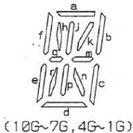
7.1.2 DISPLAY
■ RAW1157 (SUBB UNIT : V1501)
FL Tube
● Pin Assignment
| NOTE 1) F1,F2 - Filament |
| 2) NP ---- No Pin |
| 3) NC ---- No connection |
| 4) DL ---- Datum Line |
| 5) IG~10G-- Grid |
● Pin Connection
| PIN NO. | 1 | 2 | 3 | 4 | 5 | 6 | 7 | 8 | 9 | 10 | 11 | 12 | 13 | 14 | 15 | 16 | 17 | 18 | 19 | 20 | 21 | 22 | 23 | 24 | 25 | 26 | 27 | 28 | 29 | 30 | 31 | 32 | 33 | 34 | 35 |
| CONNECTION | F | F | N | N | P | P | P | P | P | P | P | N | P | P | P | P | P | P | P | P | P | P | P | P | P | P | P | P | P | P | P | P | P | P | P |
● Grid Assignment
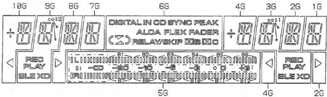
● Anode Connection
| 10G | 9G | 8G | 7G | 6G | 5G | 4G | 3G | 2G | 1G | |
| P1 | a | a | a | a | DIGITAL | B1 | a | a | a | a |
| P2 | b | b | b | b | IN | B2 | b | b | b | b |
| P3 | f | f | f | f | CD | B3 | f | f | f | f |
| P4 | g | g, m | g | g | SYNC | B4 | g | g, m | g | g |
| P5 | c | c | c | c | PEAK | B5 | c | c | c | c |
| P6 | e | e | e | e | FADER | B6 | e | e | e | e |
| P7 | d | d | d | d | FLEX | S1 | d | d | d | d |
| P8 | j, p | j, p | j, p | j, p | ALGA | - | j, p | j, p | j, p | j, p |
| P9 | m | col2 | m | m | DOB | B7 | m | col1 | m | m |
| P12 | h | n, n | h | h | DOC | B8 | h | h, n | h | h |
| P11 | k | REC | k | - | B9 | k | REC | k | - | |
| P12 | PLAY | n | n | B10 | PLAY | n | n | |||
| P13 | BLE | r | - | B11 | BLE | r | - | |||
| P14 | XD | - | RELAY/SKOF | B12 | XD | - |
CT-W706DR, CT-W606DR, CT-05D
7.2 TEST MODE
7.2.1 Entering the Test Mode
While both mechanisms are stop, press the TIME/COUNT, RESET keys of DECK I and PAUSE key of DECK II together to enter the test mode. (Refer to Fig. 1)
7.2.2 Exiting the Test Mode
● Press the RESET key of DECK I.
● Press the STANDBY key.
● Turn off the power.
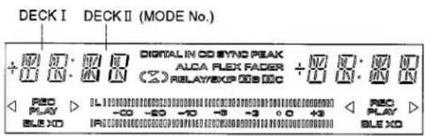
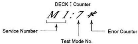
Fig. 1 FL Display Example
7.2.3 Shifting to Test Mode State
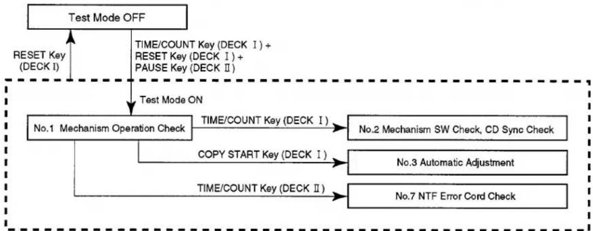
flowchart
graph TD
    A["Test Mode OFF"] --> B["No.1 Mechanism Operation Check"]
    B --> C["TIME/COUNT Key (DECK I) + RESET Key (DECK I) + PAUSE Key (DECK II)"]
    B --> D["TIME/COUNT Key (DECK I)"]
    B --> E["COPY START Key (DECK I)"]
    B --> F["TIME/COUNT Key (DECK II)"]
    C --> G["No.2 Mechanism SW Check, CD Sync Check"]
    E --> H["No.3 Automatic Adjustment"]
    F --> I["No.7 NTF Error Cord Check"]
    J["RESET Key (DECK I)"] --> B
* During the test mode, pressing the STOP key (DECK I or DECK II) will set test mode No. 1.
7.2.4 Main Test Mode Items
Test mode No.1 Mechanism Operation Check
Test mode No.2.... Mechanism SW Check, CD Sync Check
Test mode No.3 ...... Automatic Adjustment
Test mode No.7 ..... NTF Error Code Check
7.2.5 Test Mode No. 1 (Mechanism Operation Check)
■ Operations specifications
| DECK I Display | DECK II Display | Input Key | Adjustment and Check |
| 10 | (TUNE) | STOPFWDREVFFREWRECPAUSEMUTECOPY MODECOPY START | ◇ The mechanism operates without the half in this mode.◇ Test speed adjustmentDuring PLAY (except in assisting), when FF or REW key is pressed, ×2 speed PLAY is set.During ×2 speed PLAY , when FWD or REV key is pressed, constant speed PLAY is set.◇ Auto stop checkSets RELAY ON forcibly.However no relay during REC.Even at tape end directly after PLAY, the auto stop time is 1 second. (Normally 4 seconds)Reverse operations are normally performed. |
When automatic adjustment has been completed, "TUNE" lights on the DECK II counter.
7.2.6 Test Mode No. 2 (Mechanism SW Check, CD Sync Check)
■ Entering the Mechanism SW check mode
Press the TIME/COUNT key.
■ Exiting the Mechanism SW check mode
When the STOP key (DECK I or DECK II) is pressed, test mode No. 1 is set.
■ Operations specifications
| DECK I Display | DECK II Display | Input Key | Line Mute | REC Mute | Bias | Adjustment and Check |
| 20 | ON | ON | OFF | ◇ SW checkWhen there is a half, each counter shows “H” at the second digit from the left.Accidental erasure detection checkFWD recordable: "►" lights up (DECK II)REV recordable: "◄" lights up (DECK II)Tape type checkWhen there is a tape, display is made at the first digit from the left on the counter.NORMAL TAPE : "n"CrO2 TAPE : "C"METAL TAPE : "M"◇ Door open / close check (CT-W706DR only)When the side 1 door is open /close, display is made at the 3rd digit from the left on the side 2 counter.When the side 2 door is open /close, display is made at the 4th digit from the left on the side 2 counter.OPEN : "O"CLOSE : "C" | ||
| CD SYNC | ◇ CD sync checkWhen the cord whose input and output are short-circuited is connected, and the CD SYNCHRO key is pressed, "CD SYNC" display lights up. |
7.2.7 Test Mode No. 3 (Automatic Adjustment)
For details, refer to "6. ADJUSTMENT".
| DECK I Display | DECK II Display | Input Key | Adjustment and Check |
| PBR | PBR | STOPFWDREVREC | 1Press the COPY START key to enter the test mode.2When the REC key (DECK II) is pressed.4Execute adjustment of recording bias and recording level.5When all adjustments have been completed. “PBR” lights on the DECK II side counter.6When the STOP key (DECK I or DECK II) is pressed, test mode No. 1 is set. |
CT-W706DR, CT-W606DR, CT-05D
7.2.8 Test Mode No. 7 (NTF Error Code Check Mode)
■ Entering the NTF error code check mode
Press the TIME/COUNT key of DECK II.
When pressed again, the counter changes as follows.
$$ 1 \Rightarrow 2 \Rightarrow 3 \Rightarrow 1 $$
■ Exiting the NTF error code check mode
- When the STOP key (DECK I) is pressed, test mode No. 1 is set.
- When repair has been completed, reset the recorded error. (Press the STOP key, and press the TIME/COUNT key (DECK I) and the MUTE key (DECK II) immediately after entry into test mode.)
■ NTF error code check mode display
■ Operations specifications
| Error Location | Service No. | State of Unit | Cause |
| BLE | B1 (DECK II)B3 (DECK I) | BLE Adjustment Error | The take-up side reel table stops during BLE operations.The sensor at the reel table is faulty.Tape end is set. |
| B2 (DECK II)B4 (DECK I) | BLE Adjustment Error | The signals were not recorded during BLE operations. | |
| Mechanism | M3 | DECK I is locked | The mechanism and the half are engaged in DECK I . |
| M4 | DECK II is locked | The mechanism and the half are engaged in DECK II . | |
| Cassette door | L1 | Door loading of side 1 | It put top and bottom of Tape adversely and was going to close a door.A door hits an obstacle, and a door doesn't finish opening . |
| L2 | Door loading of side 2 |
* B3 and B4 on the DECK I side and B1 and B2 on the DECK II side light for the error No. of BLE errors.
■ Resetting the error code
To reset, press the TIME/COUNT key of DECK I and MUTE key of DECK II together.
7.3 BLOCK DIAGRAM
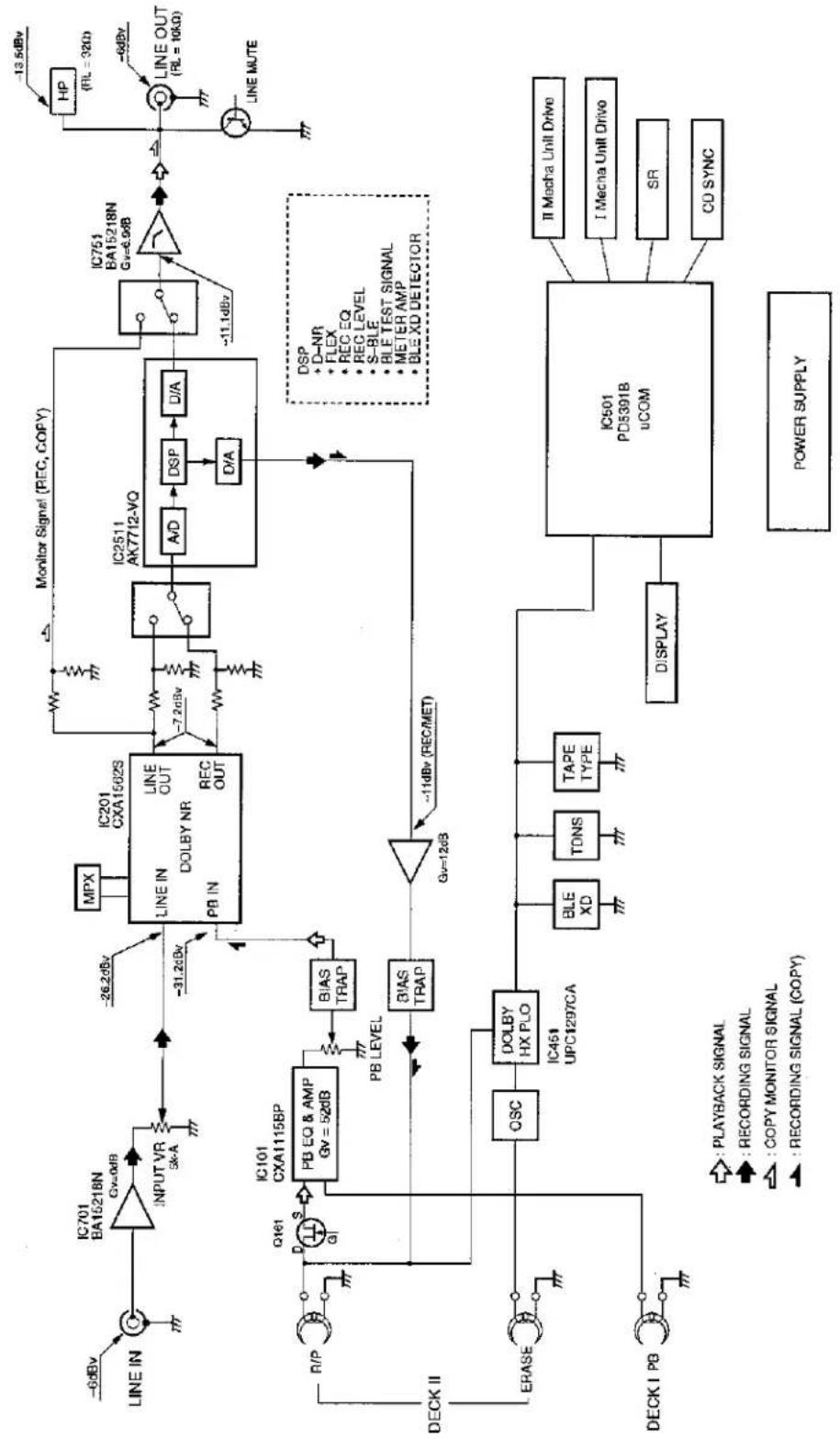
flowchart
graph TD
    A["LINE IN"] --> B["IC701 BA1521BN Gv=0dB"]
    B --> C["INPUT VR 5kA"]
    C --> D["LINE IN"]
    D --> E["IC201 CXA1562S"]
    E --> F["DOLBY NR"]
    F --> G["PB IN"]
    G --> H["BIAS TRAP"]
    H --> I["CB"]
    I --> J["DOLBY HX PLO"]
    J --> K["IC451 UPC1297CA"]
    K --> L["BLE XD"]
    K --> M["TDNS"]
    K --> N["TAPE TYPE"]
    N --> O["IC501 PD5391B uCOM"]
    O --> P["POWER SUPPLY"]

    subgraph Power Supply
        Q["POWER SUPPLY"] --> R["Display"]
        S["Power Supply"] --> T["IC501 PD5391B uCOM"]
        U["Power Supply"] --> V["IC751 BA15218N Gv=6.9dB"]
        W["Power Supply"] --> X["IC751 BA15218N Gv=6.9dB"]
        Y["Power Supply"] --> Z["IC751 BA15218N Gv=6.9dB"]
        AA["Power Supply"] --> AB["IC751 BA15218N Gv=6.9dB"]
        AC["Power Supply"] --> AD["IC751 BA15218N Gv=6.9dB"]
        AE["Power Supply"] --> AF["IC751 BA15218N Gv=6.9dB"]
        AG["Power Supply"] --> AH["IC751 BA15218N Gv=6.9dB"]
        AI["Power Supply"] --> AJ["IC751 BA15218N Gv=6.9dB"]
        AK["Power Supply"] --> AL["IC751 BA15218N Gv=6.9dB"]
        AM["Power Supply"] --> AN["IC751 BA15218N Gv=6.9dB"]
        AO["Power Supply"] --> AP["IC751 BA15218N Gv=6.9dB"]
        AQ["Power Supply"] --> AR["IC751 BA15218N Gv=6.9dB"]
        AS["Power Supply"] --> AT["IC751 BA15218N Gv=6.9dB"]
        AU["Power Supply"] --> AV["IC751 BA15218N Gv=6.9dB"]
        AW["Power Supply"] --> AX["IC751 BA15218N Gv=6.9dB"]
        AY["Power Supply"] --> AZ["IC751 BA15218N Gv=6.9dB"]
        BA["Power Supply"] --> BB["IC751 BA15218N Gv=6.9dB"]
        BC["Power Supply"] --> BD["IC751 BA15218N Gv=6.9dB"]
        BE["Power Supply"] --> BF["IC751 BA15218N Gv=6.9dB"]
        BG["Power Supply"] --> BH["IC751 BA15218N Gv=6.9dB"]
        BI["Power Supply"] --> BJ["IC751 BA15218N Gv=6.9dB"]
        BK["Power Supply"] --> BL["IC751 BA15218N Gv=6.9dB"]
        BM["Power Supply"] --> BN["IC751 BA15218N Gv=6.9dB"]
        BO["Power Supply"] --> BP["IC751 BA15218N Gv=6.9dB"]
        BQ["Power Supply"] --> BR["IC751 BA15218N Gv=6.9dB"]
        BS["Power Supply"] --> BT["IC751 BA15218N Gv=6.9dB"]
        BU["Power Supply"] --> BV["IC751 BA15218N Gv=6.9dB"]
        BW["Power Supply"] --> BX["IC751 BA15218N Gv=6.9dB"]
        BYD["Power Supply"] --> BZ["IC751 BA15218N Gv=6.9dB"]
        BZL["Power Supply"] --> BW
    end

    subgraph Power Supply
        BQL["R/P"] --> CC["GqI"]
        CC --> DD["I/O"]
        DD --> DP["PB EQ & AMP Gv = 52dB"]
        DP --> DD
        DD --> EE["PB LEVEL"]
        EE --> FF["BIAS TRAP"]
        FF --> GG["Bias Trap"]
        GG --> HH["Gv=12dB"]
        HH --> ID["-11dB (REC/MET)"]
    end

    subgraph Power Supply
        BB["R/CEK II"] --> BC
        BC --> DD
        DD --> DD
        DD --> EE
        EE --> F
        FF --> GG
        GG --> H
    end

    subgraph Power Supply
        BI["R/CEK II"] --> BJ["CSC"]
        BJ --> BK["DOLBY HX PLO"]
        BK --> BL["IC451 UPC1297CA"]
        BL --> BM["BLE XD"]
        BM --> BN["TDNS"]
        BN --> BO["TAPE TYPE"]
    end

    subgraph Power Supply
        BI["R/CEK II"] --> BJ
        BJ --> BK
    end

    subgraph Power Supply
        BI["R/CEK II"] --> BJ
        BJ --> BK
    end

    subgraph Power Supply
        BI["R/CEK II"] --> BJ
        BJ --> BK
    end

    subgraph Power Supply
        BI["R/CEK II"] --> BJ
        BJ --> BK
    end

    subgraph Power Supply
        BI["R/CEK II"] --> BJ
        BJ --> BK
8. PANEL FACILITIES AND SPECIFICATIONS
PANEL FACILITIES
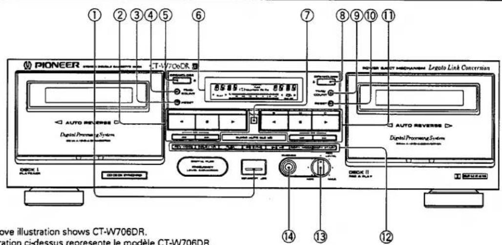
① STANDBY/ON switch
The STANDBY/ON switch activates the secondary transformer only. Even when the switch is in the STANDBY position, there will be a power flow to the deck's circuits as long as the power cord is connected to a power outlet.
When the STANDBY/ON switch is left ON, standby mode is controlled by the connected amplifier's System Remote Control spI function. Press the POWER button on the remote control unit to select the standby mode. This mode is displayed as "ST-BY" on the DECK II counter.(except for Canadian model)
② Deck I operation buttons
: Reverse playback
: Stop
: Forward playback
←/MS : Fast reverse/music search
▶/MS : Fast forward/music search
③ DECK I counter reset button (RESET)
④ DECK I counter mode button (TIME/COUNT)
⑤ DECK I OPEN/CLOSE button (CT-W706DR)
DECK I EJECT button (CT-W606DR, CT-W616DR) (▲)
- If the tape is moving (playback, tape winding, etc.), press the stop (■) button before pressing this button.
NOTE:
If the power is turned off while the tape is moving, the cassette door may remain locked. In this case, turn the power on before pressing the eject (▲) button.
⑥ Function display
⑦ Digital indicator
Turns off while the Digital-NR is OFF.
⑧ DECK II OPEN/CLOSE button (CT-W706DR)
DECK II EJECT button (CT-W606DR, CT-W616DR) (▲)
- If the tape is moving (recording, playback, tape winding, etc.), press the stop (■) button before pressing this button.
NOTE:
If the power is turned off while the tape is moving, the cassette door may remain locked. In this case, turn the power on before pressing the eject (▲) button.
⑨ DECK II counter mode button (TIME/COUNT)
⑩ DECK II counter reset button (RESET)
⑪ DECK II operation buttons
: Reverse playback
: Stop
: Forward playback
◄◄/MS : Fast reverse/music search
▶/MS : Fast forward/music search
0 : Recording mute
|| : Pause
: Recording
⑫ REV MODE button
DOLBY\* NR button (OFF/B/C)
• Dolby noise reduction and HX Pro headroom extension manufactured under license from Dolby Laboratories Licensing Corporation. HX Pro originated by Bang & Olufsen.
- "DOLBY", the double-D symbol and "HX PRO" are trademarks of Dolby Laboratories Licensing Corporation.
FLEX button
CD-DECK SYNCHRO recording button (CD SYNC).
BLE XD button
COPY MODE button
TDNS : TDNS copy (Normal speed copy).
NOR : Normal speed copy.
HI : High speed copy.
COPY START button
⑬ Recording level control (REC LEVEL)
⑭ Headphones jack (PHONES)
SPECIFICATIONS
System 4-track, 2-channel stereo
Heads .... "Hard Permalloy" recording/playback head x 1
"Hard Permalloy" playback head x 1
"Ferrite" erasing head x 1
Motor DC servo motor x 2
Loading motor x 2 (CT-W706DR)
Wow and Flutter 0.09% (WRMS)
±0.19% (DIN)
Fast Winding Time..... Approximately 100 seconds (C-60 tape)
Frequency Response
-20 dB recording
TYPE IV (Metal) tape 20 to 20.000 Hz
TYPE II (High/CrO2) tape 20 to 19.000 Hz
TYPE I (Normal) tape 20 to 18.000 Hz
Signal-to-Noise Ratio
Dolby NR OFF More than 57 dB
Signal-to-Noise Ratio (when Digital NR ON)
Dolby NR B or C-type ON 90 dB
Dolby NR OFF 82 dB
(TYPE I tape, 3rd distortion 3%, IEC. DIN AUDIO)
Harmonic Distortion No more than 0.8%
(at -4 dB: 160 nwb/m)
Input (Sensitivity)
LINE (INPUT) 100 mV (Input impedance 53 kΩ)
Output (Reference level)
LINE (OUTPUT) 0.5 V (Output impedance 1.9 kΩ)
Headphones 1.33 mW (Load impedance 32 Ω)
Miscellaneous
Power Requirements
Canadian model AC 120 V, 60 Hz
European models AC 220-230 V, 50/60 Hz
Multi-voltage models....AC 110/120-127/220/230-240V
(switchable), 50/60 Hz
Power Consumption
Canadian model 17 W
European models 19 W
Multi-voltage models....19 W
Dimensions 420(W) × 125(H) × 250(D) mm
16-1/2 (W) x 4-15/16 (H) x 9-13/16 (D) in
Weight (without package)
Canadian models 4.4kg (9 lb 11 oz)
European model 4.4kg (9 lb 11 oz)
Multi-voltage models.... 4.4kg (9 lb 11 oz)
Subfunctions
• Automatic reverse
● Music search up to ±15 selections
- Synchronized copy start
- High-speed and normal-speed copy (DECK I → DECK II)
- Relay playback/blank skip
- CD-DECK SYNCHRO recording capability
● Peak level meter with peak-hold function
● Automatic space recording mute
● Automatic tape selector
• System remote control available
● 2-mode electronic 4-digit twin tape counter
- Headphone jack
● DIGITAL FLEX system (Frequency Level Expander)
• DIGITAL TDNS system (Tape Duplication Noise Suppressor)
• DIGITAL SUPER AUTO BLE XD system
LAST MEMORY
• DIGITAL NR
● Legato Link Conversion (CT-W706DR, CT-05D)
● Power Loading/Eject (CT-W706DR)
● MPX filter (Interlocks with DOLBY NR)
Accessories
Operating instructions ....1
Connection cord with pin plugs 2
SR Remote control cord 1
CD-DECK SYNCHRO control cord 1
NOTE:
Specifications and design subject to possible modifications without notice, due to improvements.
- STEREO DOUBLE CASSETTE DECK
- CT-W706DR
- CT-W606DR
- CT-05D
- CONTENTS
- SAFETY INFORMATION
- WARNING
- NOTICE
- REMARQUE
- LEAKAGE CURRENT CHECK
- PRODUCT SAFETY NOTICE
- EXPLODED VIEWS AND PARTS LIST
- CONTRAST TABLE
- ● For CT-W706DR and CT-05D
- ● For CT-W606DR
- CT-W706DR, CT-W606DR, CT-05D
- CONTRAST TABLE for CT-W706DR
- CONTRAST TABLE for CT-W606DR and CT-05D
- 1 MECHANISM AND 2 MECHANISM UNITS
- SCHEMATIC DIAGRAM
- OVERALL WIRING DIAGRAM
- MAIN UNIT (3/4), MOTOR 1, MOTOR 2, EJECT 1 AND EJECT 2 UNITS
- PCB CONNECTION DIAGRAM
- PCB PARTS LIST
- LIST OF WHOLE PCB ASSEMBLIES
- CONTRAST OF PCB ASSEMBLIES
- MAIN UNIT
- B TRANS UNIT
- OTHERS
- C SUBB UNIT
- SEMICONDUCTORS
- SWITCHES
- CAPACITOR
- RESISTORS
- D MOTOR 1 UNIT
- EJECT 1 UNIT
- SWITCH
- F MOTOR 2 UNIT
- G EJECT 2 UNIT
- ADJUSTMENT
- MECHANICAL ADJUSTMENT
- Door Damping Check and Adjustment (except CT-W706DR)
- Tape Speed Adjustment
- ELECTRICAL ADJUSTMENT
- Adjustment Conditions
- List of Adjustments
- Playback Section
- Head Azimuth Adjustment
- Playback Level Adjustment
- Recording Section
- GENERAL INFORMATION
- PARTS
- AK7712-VQ (MAIN UNIT : IC2511)
- ● DSP
- DISPLAY
- ■ RAW1157 (SUBB UNIT : V1501)
- FL Tube
- ● Pin Assignment
- ● Pin Connection
- ● Grid Assignment
- ● Anode Connection
- TEST MODE
- Entering the Test Mode
- Exiting the Test Mode
- Shifting to Test Mode State
- Main Test Mode Items
- Test Mode No. 1 (Mechanism Operation Check)
- ■ Operations specifications
- Test Mode No. 2 (Mechanism SW Check, CD Sync Check)
- ■ Entering the Mechanism SW check mode
- ■ Exiting the Mechanism SW check mode
- Test Mode No. 3 (Automatic Adjustment)
- Test Mode No. 7 (NTF Error Code Check Mode)
- ■ Entering the NTF error code check mode
- ■ Exiting the NTF error code check mode
- ■ NTF error code check mode display
- ■ Resetting the error code
- PANEL FACILITIES AND SPECIFICATIONS
- PANEL FACILITIES
- ① STANDBY/ON switch
- ② Deck I operation buttons
- NOTE:
- ⑪ DECK II operation buttons
- ⑫ REV MODE button
- DOLBY\* NR button (OFF/B/C)
- FLEX button
- CD-DECK SYNCHRO recording button (CD SYNC).
- BLE XD button
- SPECIFICATIONS
- Miscellaneous
- Subfunctions
- Accessories
Brand : PIONEER
Model : CT-05D
Category : Cassette player