
TM-D710E - Ham Radio KENWOOD - Free user manual and instructions
Find the device manual for free TM-D710E KENWOOD in PDF.
| Product type | Single-unit mobile amateur radio transceiver |
| Brand | Kenwood |
| Model | TM-D710E |
| Frequency bands | VHF (144-146 MHz), UHF (430-440 MHz) |
| Output power | 50 W (VHF), 35 W (UHF) |
| Power supply | 13.8 V DC ±15%, negative ground |
| Power consumption | Transmit: max. 11 A; receive: max. 1.5 A |
| Dimensions (W × H × D) | 140 × 40 × 185 mm (without projections) |
| Weight | Approx. 1.2 kg |
| Display | Dot matrix LCD, backlit |
| Modulation modes | F3E (FM), F2D (AFSK), G3E (FM with subaudible) |
| Number of memories | 200 channels + 10 search channels |
| APRS functions | Built-in TNC modem, GPS positioning, messaging |
| PC interface | Serial port (RS-232C) via 6-pin jack connector |
| Antenna | SO-239 connector (50 Ω) |
| Maintenance and cleaning | Wipe with a dry soft cloth; do not use solvents |
| Safety | Use a 15 A fuse; disconnect power before any maintenance |
| Spare parts and repairability | Part numbers available in the manual's schematic; use genuine Kenwood parts |
| Included accessories | Microphone (KMC-30), mounting bracket, wiring kit, screws |
Frequently Asked Questions - TM-D710E KENWOOD
User questions about TM-D710E KENWOOD
0 question about this device. Answer the ones you know or ask your own.
Ask a new question about this device
Download the instructions for your Ham Radio in PDF format for free! Find your manual TM-D710E - KENWOOD and take your electronic device back in hand. On this page are published all the documents necessary for the use of your device. TM-D710E by KENWOOD.
USER MANUAL TM-D710E KENWOOD
This service manual details the panel section. Refer to the TM-V71A/V71E service manual (B51-8791-00) for any information which has not been covered in this TM-D710A/D710E service manual.
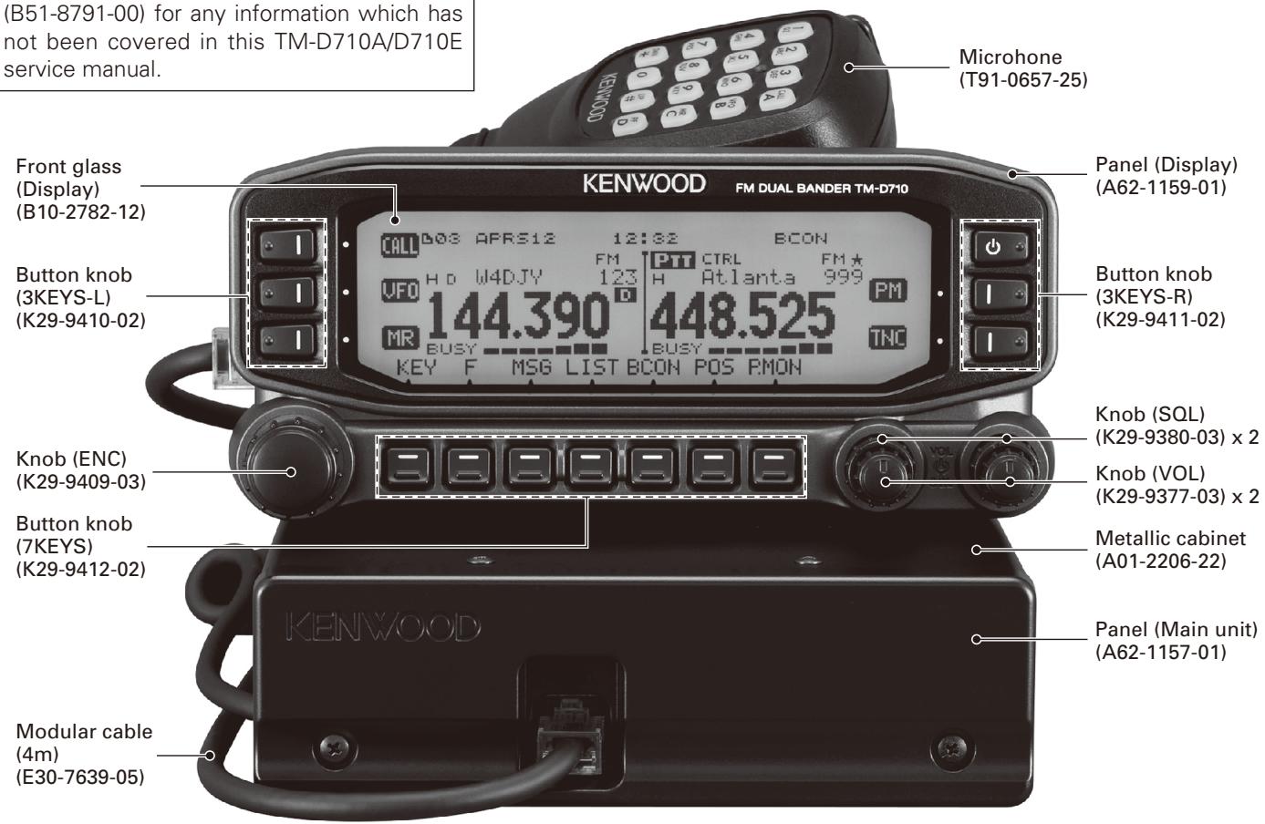
Photo is TM-D710A.
CONTENTS
CIRCUIT DESCRIPTION ...... 2
SEMICONDUCTOR DATA......6
COMPONENTS DESCRIPTION......9
TERMINAL FUNCTION 10
PARTS LIST 12
EXPLODED VIEW 29
PACKING....30
ADJUSTMENT 31
PC BOARD
DISPLAY UNIT (X54-3620-00) 52
TX-RX UNIT (X57-731X-XX) 56
INTERCONNECTION DIAGRAM 64
SCHEMATIC DIAGRAM 66
BLOCK DIAGRAM 80
LEVEL DIAGRAM 82
OPTIONAL ACCESSORIES 84
SPECIFICATIONS 85
Document Copyrights
Copyright 2007 by Kenwood Corporation. All rights reserved.
No part of this manual may be reproduced, translated, distributed, or transmitted in any form or by any means, electronic, mechanical, photocopying, recording, or otherwise, for any purpose without the prior written permission of Kenwood.
Disclaimer
While every precaution has been taken in the preparation of this manual, Kenwood assumes no responsibility for errors or omissions. Neither is any liability assumed for damages resulting from the use of the information contained herein. Kenwood reserves the right to make changes to any products herein at any time for improvement purposes.
CIRCUIT DESCRIPTION
1. Outline
TM-D710A/D710E and TM-V71A/V71E have a common main unit. Thus, the main unit firmware is also common to both.
The command formats of the panel connected to the main unit are different for TM-V71A/V71E and TM-D710A/D710E. So, the main unit section MPU (IC918) judges the type of the panel connected, when power is turned on and communication starts.
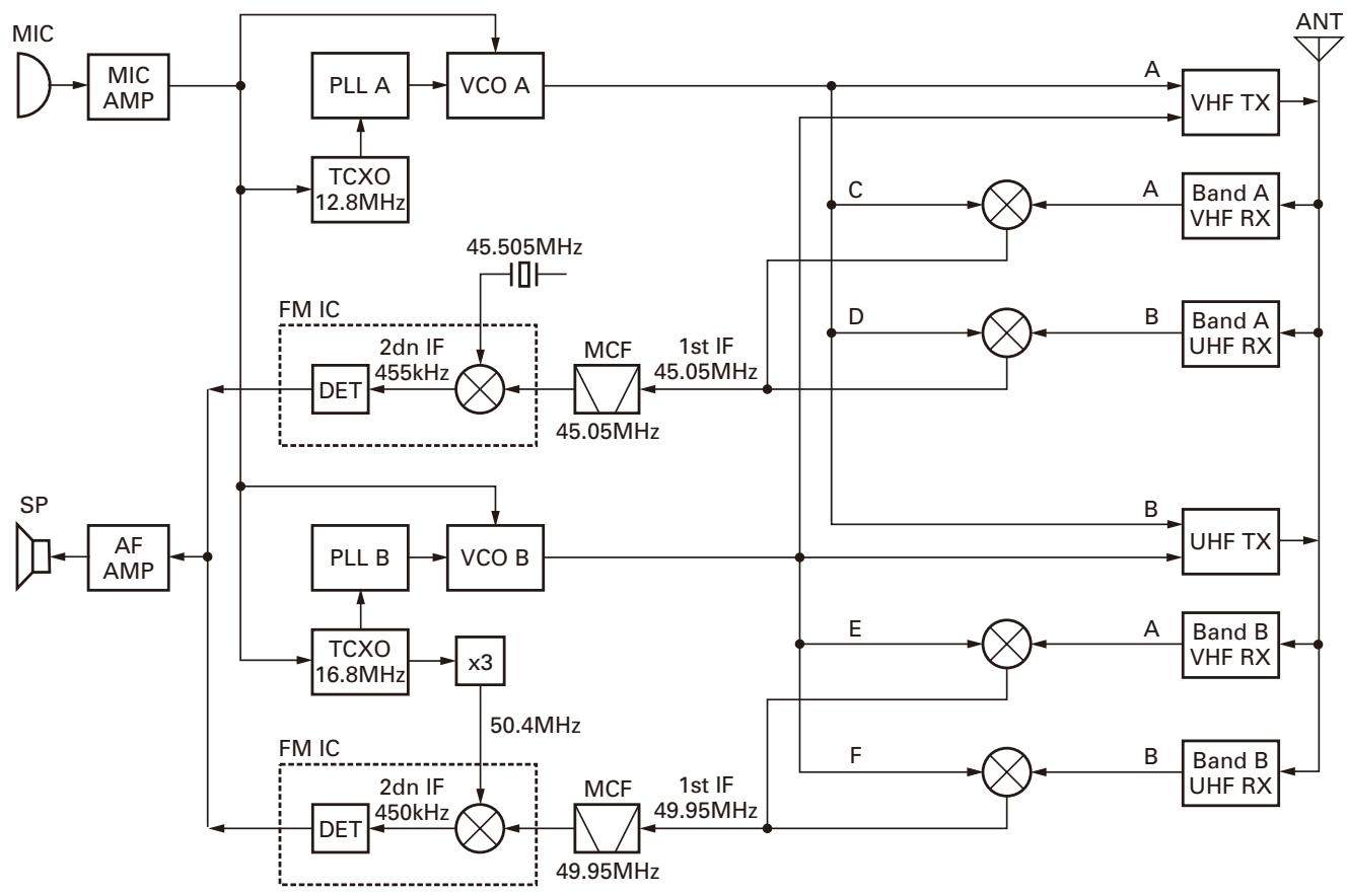
2. Frequency Configuration
The TM-D710A/D710E has an individual VCO and PLL unit for both band A and band B. Using these separate VCO and PLL circuits, it can receive 2 separate bands at the same time. You can also perform full-duplex operation.
The band A VCO is used for the following functions:
(i) VHF/UHF transmission
(ii) The first local oscillator for the band A (VHF) reception.
(iii) The first local oscillator for the band A (UHF) reception.
The band B VCO is used for the following functions:
(i) VHF/UHF transmission
(ii) The first local oscillator for the band B (VHF) reception.
(iii) The first local oscillator for the band B (UHF) reception.
The PLL reference frequency is generated by a 12.8MHz (band A) and a 16.8MHz (band B) crystal oscillator connected to the band A and band B PLL ICs. This reference frequency is used for both PLL circuits. The 45.505MHz second local oscillator for band A is generated by the FM IC crystal oscillator circuit. The second local oscillator for the band B uses the tripled 16.8MHz reference oscillator frequency.
Note:
The PCB layout and the mounting parts are the same for the band A VCO (X57-731 B/6) and band B VCO (X57-731 C/6), although the PCB silk print is different.
CIRCUIT DESCRIPTION
flowchart
graph TD
    A["SP"] --> B["AF AMP"]
    B --> C["PLL B"]
    C --> D["TCXO 16.8MHz"]
    D --> E["x3"]
    E --> F["FM IC"]
    F --> G["DET"]
    G --> H["2dn IF 450kHz"]
    H --> I["×"]
    I --> J["45.05MHz"]
    J --> K["MCF"]
    K --> L["1st IF 45.05MHz"]
    L --> M["ET"]
    M --> N["PLL A"]
    N --> O["VCO A"]
    O --> P["A"]
    P --> Q["VHF TX"]
    Q --> R["ANT"]
    S["FM IC"] --> T["DET"]
    U["FM IC"] --> V["×"]
    W["FM IC"] --> X["×"]
    Y["FM IC"] --> Z["×"]
    AA["FM IC"] --> AB["×"]
    AC["FM IC"] --> AD["×"]
    AE["FM IC"] --> AF["×"]
    AG["A"] --> AH["B"]
    AI["A"] --> AJ["B"]
    AK["A"] --> AL["B"]
    AM["A"] --> AN["B"]
    AO["A"] --> AP["B"]
    AQ["A"] --> AR["B"]
    AS["A"] --> AT["B"]
    AU["A"] --> AV["B"]
    AW["A"] --> AX["B"]
    AY["A"] --> AZ["B"]
    BA["B"] --> BB["B"]
    BC["B"] --> BD["B"]
    BE["B"] --> BF["B"]
    BG["A"] --> BH["B"]
    BI["A"] --> BJ["B"]
    BK["A"] --> BL["B"]
    BM["A"] --> BN["B"]
    BO["A"] --> BP["B"]
    BQ["A"] --> BR["B"]
    BS["A"] --> BT["B"]
    BU["A"] --> BV["B"]
    BW["A"] --> BX["B"]
    BY["A"] --> BZ["B"]
    CA["A"] --> CB["B"]
    CC["A"] --> CD["B"]
    CE["A"] --> CF["B"]
    CG["A"] --> CH["B"]
    CI["A"] --> CJ["B"]
    CK["A"] --> CL["B"]
    CM["A"] --> CN["B"]
    CO["A"] --> CP["B"]
    CS["A"] --> CY["B"]
    CZ["A"] --> CE
| K type | E type | M4 type | |
| A | 144.000 ~147.995MHz | 144.000~145.995MHz | 144.000~145.995MHz |
| B | 438.000~449.995MHz | 430.000~439.995MHz | 430.000~439.995MHz |
| C | 189.050~193.045MHz | 189.050~191.045MHz | 189.050~191.045MHz |
| D | 392.950~404.945MHz | 384.950~394.945MHz | 384.950~394.945MHz |
| E | 193.950~197.945MHz | 193.950~195.945MHz | 193.950~195.945MHz |
| F | 388.050~400.045MHz | 380.050~390.045MHz | 380.050~390.045MHz |
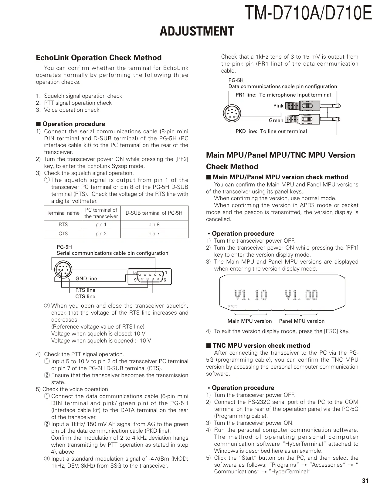
Fig. 1 Frequency configuration
Band A 1st IF: 45.05MHz, 2nd IF: 455kHz (Upper)
| RX frequency range [MHz] | VCO oscillation frequency range [MHz] | Multiply | VCO V/U IC576 pin 7 | VCO shift IC576 pin 12 | 1st Mix. | Local frequency range [MHz] | |||
| 118.000 | 129.995 | 163.050 | 175.045 | 1 | H | L | Upper | 163.050 | 175.045 |
| 130.000 | 185.995 | 175.050 | 231.045 | 1 | H | H | Upper | 175.050 | 231.045 |
| 186.000 | 224.995 | 140.950 | 179.945 | 1 | H | L | Lower | 140.950 | 179.945 |
| 225.000 | 279.995 | 179.950 | 234.945 | 1 | H | H | Lower | 179.950 | 234.945 |
| 280.000 | 359.995 | 325.050 | 405.045 | 1 | L | L | Upper | 325.050 | 405.045 |
| 360.000 | 399.995 | 405.050 | 445.045 | 1 | L | H | Upper | 405.050 | 445.045 |
| 400.000 | 429.995 | 354.950 | 384.945 | 1 | L | L | Lower | 354.950 | 384.945 |
| 430.000 | 523.995 | 384.950 | 478.945 | 1 | L | H | Lower | 384.950 | 478.945 |
TM-D710A/D710E
CIRCUIT DESCRIPTION
Band B 1st IF: 49.95MHz, 2nd IF: 450kHz (Upper)
| RX frequency range [MHz] | VCO oscillation frequency range [MHz] | Multiply | VCO V/U IC577 pin 7 | VCO shift IC577 pin 12 | 1st Mix. | Local frequency range [MHz] | |||
| 136.000 | 185.995 | 185.950 | 235.945 | 1 | H | H | Upper | 185.950 | 235.945 |
| 186.000 | 224.995 | 136.050 | 175.045 | 1 | H | L | Lower | 136.050 | 175.045 |
| 225.000 | 279.995 | 175.050 | 230.045 | 1 | H | H | Lower | 175.050 | 230.045 |
| 280.000 | 359.995 | 329.950 | 409.945 | 1 | L | L | Upper | 329.950 | 409.945 |
| 360.000 | 399.995 | 409.950 | 449.945 | 1 | L | H | Upper | 409.950 | 449.945 |
| 400.000 | 429.995 | 350.050 | 380.045 | 1 | L | L | Lower | 350.050 | 380.045 |
| 430.000 | 523.995 | 380.050 | 474.045 | 1 | L | H | Lower | 380.050 | 474.045 |
| 800.000 | 823.990 | 375.0250 | 387.0200 | 2 | L | L | Lower | 750.050 | 774.040 |
| 824.000 | 909.990 | 436.9750 | 479.9700 | 2 | L | H | Upper | 873.950 | 959.940 |
| 910.000 | 1109.990 | 319.9833 | 386.6467 | 3 | L | L | Upper | 959.950 | 1159.940 |
| 1100.000 | 1209.990 | 350.0167 | 386.6800 | 3 | L | L | Lower | 1050.050 | 1160.040 |
| 1210.000 | 1299.990 | 314.9875 | 337.4850 | 4 | L | L | Upper | 1259.950 | 1349.940 |
RX BPF switching frequency
| VHF BPF | UHF BPF | |
| Band A | 118~279.995MHz (5RVA : ON) | 280~523.995MHz (5RUA : ON) |
| Band B | 136~279.995MHz (5RVB : ON) | 280~523.995MHz (5RUB : ON) |
VHF BPF shift frequency
| BPF shift switch | RX frequency | |
| ~199.995MHz | 200MHz~ | |
| IC576 pin 16 | L | H |
| IC577 pin 17 | L | H |
3. Panel Section
The panel section consists of the control section, the TNC section and the full-dot LCD (235×65 dots) display section.
The flash-type panel MPU (IC1) is used in the panel section and the firmware can be rewritten. Also, the panel MPU has no program for controlling frequency, so it is common for all types.
3-1. Power Supply Circuit
10V is always supplied to the panel section even if the power of the main unit is turned off, as long as the main unit is connected to a power supply such as battery. Power is applied to the panel MPU through the 5V AVR (IC6) and the panel section is operating in standby mode.
When in standby state, the LCD power, the RS-232C circuit power and the TNC power are turned off with switches Q1, Q2, and Q3 respectively, in order to reduce power consumption.
The reset signal of the panel MPU (IC1) detects the rising edge of the voltage of the 5V line with the voltage detection
IC (IC3). The voltage detection IC (IC24) detects the reduced voltage of the 10V power line and backs up the state immediately before the voltage becomes approximately 8V or less, to the EEPROM (IC2).
The voltage detection IC (IC14) monitors the TNC-5V line and the reset signal of the TNC MPU (IC11) performs reset operations.
The backup battery circuit divides the 5V voltage always applied with R115 and R116 and floating-charges the internal rechargeable lithium battery through the reverse current prevention diode (D3). The voltage of the battery is approximately 3.1V when fully charged.
The internal rechargeable lithium battery backs up the data of the S-RAM (IC13), RTC (IC25) and logic IC (IC15). The backup current of approximately 5 A is consumed. So, the data can be saved for approximately four weeks on a full charge.
The S-RAM is used for maintaining the status of the packet mode.
The call sign of the APRS and reception list are stored in the EEPROM.
CIRCUIT DESCRIPTION
3-2. Key, Encoder, Volume Input Circuit
The panel section key corresponds to the panel MPU port, one-to-one. The POWER key is pulled up and connected to the interrupt port of the panel MPU.
Other keys are also pulled up outside because the panel MPU is an 8 bit data bus mode. The scanning process reads out the status of the keys. So, if a key is in the "L" level, no other keys are accepted.
The encoder is connected to the panel MPU and the port is pulled up.
The volume (VOL/SQL) divides the 5V voltage, reads with the A/D port of the panel MPU and transfers the data to the main unit section MPU (IC918).
3-3. Display Circuit
The LCD is a COF (Chip On Flexible printed circuit board) type with the driver IC mounted on the FPC and controlled by the 8 bit data bus mode. The voltage "V3" is approximately 12V for the LCD, but due to the voltage booster function of this driver IC, it can operate with a single power of 5V.
The contrast can change this "V3" voltage by 16 steps, using the internal memory of the driver IC.
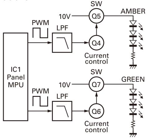
3-4. Brightness Circuit
The illumination color can be set to either amber or green.
The PWM signal output from the panel MPU passes through the LPF, is converted into DC voltage, and controls the current that flows to the LED with the transistor. The duty of the PWM changes the LED brightness to one of eight levels or OFF.
flowchart
graph TD
    A["IC1 Panel MPU"] --> B["PWM"]
    A --> C["LPF"]
    C --> D["SW Q5"]
    D --> E["AMBER"]
    C --> F["Q4"]
    F --> G["Current control"]
    H["PWM"] --> I["LPF"]
    I --> J["SW Q7"]
    J --> K["GREEN"]
    I --> L["Q6"]
    L --> M["Current control"]
Fig. 2 Brightness circuit
3-5. TNC Section
The reception data signal from the main unit is input to the panel section through the PRI terminal (pin 8 of the modular jack of the panel section). This signal is the same as the PR9 signal of the DATA terminal. So, the data signal enters the panel section through the same route for both 1200bps and 9600bps.
The reception data signal from the PRI terminal passes the LPF (gain: 0, cutoff frequency: 4.8kHz) of IC22, adjusts the output with the electric volume (IC20) and the data signal enters the operational amplifier (IC10). The output adjustment value of the electric volume is fixed. The data signal of 1200bps and 9600bps is divided with the op-amp (IC10). Each data signal passes the buffer amp and is converted to a logic signal by the comparator (IC17).
The logic signal converted with the comparator enters to the TNC ASIC (IC12). The signal is demodulated with the TNC ASIC and is then processed with the TNC MPU (IC11).
For packet mode, signals processed with the TNC MPU enter to the panel MPU. The digital signals are not changed in the panel MPU. The level of the signal is changed with the RS-232C driver IC (IC7) and the signals are then output from the COM terminal (J2).
In APRS mode, the signal entering the panel MPU is processed and the status is displayed on the LCD.
The TNC section uses the same 3-chip TNC as the TM-D700. The flash-type TNC MPU is used and the firmware can be rewritten. The MPU clock operates at double frequency. TNC ASIC is an existing product. So, the frequency of the clock signal is divided by half with the flip-flop (IC16).
The S-RAM (IC13) has a capacity of 4M bits in order to operate smoothly in the KISS mode of packet communication.
SEMICONDUCTOR DATA
Panel MPU: 30626FHPGKBXC (Display unit IC1)
| Pin No. | Port Name | I/O | Function |
| 1 | 2099EN | O | Chip enable output for serial-parallel conversion IC (BU2099FV) |
| 2 | RTC_SCL | O | RTC (RV5C386A) serial clock output (I2C bus) |
| 3 | LCD_RES | O | LCD driver reset terminal |
| 4 | CLOCK | O | Common serial clock output (EEPROM, DAC, serial-parallel) |
| 5 | DATA | O | Common serial data output (EEPROM, DAC, serial-parallel) |
| 6 | BYTE | I | Not used (5V) |
| 7 | NC | - | Not used (GND) |
| 8 | ENC_1 | I | Encoder, B |
| 9 | SQCIN | I | Squelch state input from transceiver main unit |
| 10 | RESET | I | System reset |
| 11 | XOUT | O | System clock output (11.0592MHz) |
| 12 | VSS | I | GND |
| 13 | XIN | I | System clock input (11.0592MHz) |
| 14 | VCC | I | 5V power supply |
| 15 | NMI | I | Not used (5V) |
| 16 | ENC_2 | I | Encoder, A (INT) |
| 17 | RXD_INT | I | RXD detection interrupt from main unit UART terminal |
| 18 | INT | I | Power supply voltage fall detection interrupt |
| 19 | PKSOUT | O | PKS request output to transceiver main unit |
| 20 | AMBER | O | Brightness output PWM (Amber) |
| 21 | EEPCS | O | EEPROM (AT25256A) chip select output |
| 22 | EEPSI | I | EEPROM (AT25256A) serial data input |
| 23 | DA_EN | O | DAC (M62364) chip select output |
| 24 | BEEP | O | BEEP sound output |
| 25 | INTRA | I | RTC fixed-cycle interrupt terminal |
| 26 | GREEN | O | Brightness output PWM (Green) |
| 27 | RXD(TNC) | I | UART input from internal TNC terminal |
| 28 | TXD(TNC) | O | UART output to internal TNC terminal |
| 29 | TXD | O | UART output to main unit MPU |
| 30 | RXD | I | UART input from main unit MPU |
| 31 | CLKFLS | I | Not used (GND) |
| 32 | FLS_SW | I | Not used (5V) |
| 33 | TXD(PC) | O | UART data output to PC terminal |
| 34 | RXD(PC) | I | UART data input from PC terminal |
| Pin No. | Port Name | I/O | Function |
| 35 | S9600 | I | Baud rate state input of TNC |
| 36 | PKSIN | I | Packet standby (PKS) state input of TNC |
| 37 | RDY | I | Not used (5V) |
| 38 | ALE | - | Not used |
| 39 | HOLD/EPM | I | Not used (5V) |
| 40 | HLDA | - | Not used |
| 41 | BCLK | - | Not used |
| 42 | RD | O | LCD driver RD terminal |
| 43 | BHE | - | Not used |
| 44 | WR | O | LCD driver WR terminal |
| 45 | MALED | I | Message state input to my station |
| 46 | TNCCTS | O | UART inhibiting signal output to TNC |
| 47 | TNCRTS | I | UART inhibiting signal input from TNC |
| 48 | LCD_CS0 | O | LCD driver chip select |
| 49 | KEY_4 | I | [MHz] key input |
| 50 | KEY_3 | I | [MR] key input |
| 51 | KEY_2 | I | [VFO] key input |
| 52 | KEY_1 | I | [CALL] key input |
| 53 | KEY_8 | I | [REV] key input |
| 54 | KEY_7 | I | [TONE] key input |
| 55 | KEY_6 | I | [F] key input |
| 56 | KEY_5 | I | [KEY] key input |
| 57~59 | NC | - | Not used |
| 60 | VCC | I | 5V power supply |
| 61 | NC | - | Not used |
| 62 | VSS | I | GND |
| 63~69 | NC | - | Not used |
| 70 | LCD_A0 | O | LCD driver (Address bus) |
| 71 | PSW | I | Power switch detection interrupt |
| 72 | KEY_15 | I | [PM] key input |
| 73 | KEY_14 | I | [TNC] key input |
| 74 | KEY_13 | I | [BAND SEL B] key input |
| 75 | KEY_12 | I | [BAND SEL A] key input |
| 76 | KEY_11 | I | [PF2] key input |
| 77 | KEY_10 | I | [PF1] key input |
| 78 | KEY_9 | I | [LOW] key input |
| 79~86 | LCD_D7~LCD_D0 | O | LCD driver (Data bus) |
| 87 | CONLED | I | Connection state input |
| 88 | STALED | I | The transmission remaining packet state input |
| 89 | GPSLED | I | GPS measurement state input |
SEMICONDUCTOR DATA
| Pin No. | Port Name | I/O | Function |
| 90 | RTC_SDA | I/O | RTC (RV5C386A) serial data I/O (I2C bus) |
| 91 | VOL_B | I | AF VOL (Band B) A/D input |
| 92 | VOL_A | I | AF VOL (Band A) A/D input |
| 93 | SQL_B | I | SQL (Band B) A/D input |
| 94 | AVSS | I | GND |
| 95 | SQL_A | I | SQL (Band A) A/D input |
| 96 | VREF | I | Reference voltage |
| 97 | AVCC | I | Analog power supply |
| 98 | PCCTS | I | UART inhibiting signal input from PC |
| 99 | PCRTS | O | UART inhibiting signal output to PC |
| 100 | MBLED | I | Message board connection state input |
TNC MPU: 3048BTE25KBYB (Display unit IC11)
| Pin No. | Port Name | I/O | Function |
| 1 | VCC | - | 5V power supply |
| 2 | HOSTCTS | I | CTS signal of asynchronous serial communication with host |
| 3 | SQ | I | Squelch input. H: With receive signal, L: No receive signal |
| 4 | PTT(PKSIN) | O | PTT output. H: Transmit, L: Receive |
| 5 | NC | - | Not used |
| 6 | NC | - | Not used |
| 7 | CONLED | O | CON LED Drive. H: Light off, L: Light on, During connection Light on |
| 8 | STALED | O | STALED Drive. H: Light off, L: Light on, Light on when transmit data exist. |
| 9 | NC | - | Not used |
| 10 | FWE(RESOUT) | I | Flash rewrite control |
| 11 | VSS | - | GND |
| 12 | GPSTX | O | 3 chip TNC → Serial communication host data line |
| 13 | HOSTTX | O | 3 chip TNC → Serial communication GPS data line |
| 14 | GPSRX | I | Host → Serial communication data line of 3 chip TNC |
| 15 | HOSTRX | I | GPS → Serial communication data line of 3 chip TNC |
| 16 | NC | - | L: Packet mode |
| 17 | GPSLED | O | Outputs 1-sec interval pulse when position determination data from GPS are received. |
| 18 | ABAUD1 | I | Determine the communication speed with host by combination among ABAUD1~3. Set L for 9600bps. |
| Pin No. | Port Name | I/O | Function |
| 19 | ABAUD2 | I | Determine the communication speed with host by combination among ABAUD1~3. Set L for 9600bps. |
| 20 | ABAUD3 | I | Determine the communication speed with host by combination among ABAUD1~3. Set H for 9600bps. |
| 21 | CARRIER (D3(NC)) | I | Carrier sense.L: With carrier, H: No carrier |
| 22 | VSS | - | GND |
| 23 | NC | - | Not used |
| 24 | NC | - | Not used |
| 25 | B_SEL | O | Clock divider circuit control. L: 1/2, H: 1/1 |
| 26 | NC | - | Not used |
| 27~34 | D8~D15 | I/O | Data bus of S-RAM D0~D7 |
| 35 | VCC | - | 5V power supply |
| 36~43 | A0~A7 | O | Address bus of S-RAM A0~A7 |
| 44 | VSS | - | GND |
| 45~53 | A8~A16 | O | Address bus of S-RAM A8~A16 |
| 54 | A17(NC) | O | (Address bus of S-RAM A17) |
| 55 | A18(NC) | O | (Address bus of S-RAM A18) |
| 56 | A19 | O | (Inverted to CS of S-RAM) |
| 57 | VSS | - | GND |
| 58 | WAIT | I | WAIT. H: Fixed |
| 59 | MBODLED | O | MBOD LED control.H: Light off, L: Light on |
| 60 | MAILLED | O | MAIL LED control.H: Light off, L: Light on |
| 61 | CLKOUT(NC) (CARRIER) | O | Clock output (7.9872MHz). H:Sleep |
| 62 | STBY | I | Hardware standby terminal.L: Hardware standby status (Sleep action) |
| 63 | RESET | I | Reset terminal. L: Reset status |
| 64 | SLEEP | I | Sleep terminal. H: Fixed |
| 65 | VSS | - | GND |
| 66 | X2 | I | System clock input (15.9744MHz) |
| 67 | X1 | O | System clock output (15.9744MHz) |
| 68 | VCC | - | 5V power supply |
| 69 | NC | - | Not used |
| 70 | RD(OE) | - | Connected to RD terminal of S-RAM |
| 71 | HWR | - | Connected to WR terminal of S-RAM |
| 72 | NC | - | Not used |
| 73 | MD0 | I | MPU mode setting. Normally, H |
| 74 | MD1 | I | MPU mode setting. Normally, L |
| 75 | MD2 | I | MPU mode setting. Normally, H |
TM-D710A/D710E
SEMICONDUCTOR DATA
| Pin No. | Port Name | I/O | Function |
| 76 | VCC | - | 5V power supply |
| 77 | VREF | - | 5V power supply |
| 78 | TNC_SEL(VSS) | I | LOW |
| 79 | SPEC(VSS) | I | L: Fixed |
| 80 | GPS_SEL(VSS) | I | Selects GPS default.H: SONY(9600bps), L: NMEA(4800bps) |
| 81 | PLLOCK | I | Input from gate array |
| 82 | CLKEN(VSS) | I | MPU clock output selection.H: Output, L: No output |
| 83 | FLAG | I | Input from gate array |
| 84 | SIN | I | Inputs receive serial data from gate array |
| 85 | IODATA | I | Not used (GND) |
| 86 | VSS | - | Analog circuit GND |
| 87 | SCLKR | I | Clock input of receive data from gate array |
| 88 | SCLKT | I | Clock output of transmit data to gate array |
| 89 | IOCLK | I | Not used (GND) |
| 90 | IOEN | I | Extended output port data fixed control |
| 91 | NC | - | Not used |
| 92 | VSS | - | GND |
| 93 | SOUT | O | Serial data output to gate array |
| 94 | TXX | O | Transmit/receive switch output to gate array. H: Transmit, L: Receive |
| 95 | S9600 | O | Output of gate array.H: 9600bps, L: 1200bps switch |
| 96 | WAY2 | O | Output to gate array (Not used) |
| 97 | NC | - | Not used |
| 98 | LOOP | O | Output to gate array.(H: Loop back test in gate array) |
| 99 | PLLCNT | O | Output to gate array (PLL lock follow-up) |
| 100 | HOSTRTS | O | RTS signal of asynchronous serial communication with host |
| Pin No. | Port Name | Signal name | Function | Active level |
| 6 | Q0 | TNCWR | TNC flash rewrite switching terminal | L: Rewrite |
| 7 | Q1 | PKTSW | 1200bps/ 9600bps switching | L: ON |
| 8 | Q2 | TNC_SEL | Switching between packet and APRS mode | L: Packet H: APRS |
| 9 | Q3 | TNC_CAR | Carrier sense output to TNC(carrier information of transmit band) | L: With carrier H: No carrier |
| 10 | Q4 | SQCOUT | Squelch status output to TNC | L: Receive H: Transmit |
| 11 | Q5 | 32K_SW | Control of adjustment mode of RTC crystal | L |
| 12 | Q6 | S5M_C | RS-232C driver power supply control | L |
| 13 | Q7 | TNC_PSW | TNC power supply control output | L |
| 14 | Q8 | - | Not used | |
| 15 | Q9 | LCD_SW | LCD drive power supply switch (V3) | |
| 16 | Q10 | - | Not used | |
| 17 | Q11 | - | Not used |
COMPONENTS DESCRIPTION
DISPLAY UNIT (X54-3620-00)
| Ref. No. | Use / Function | Operation / Condition / Compatibility |
| IC1 | Panel MPU | |
| IC2 | EEPROM | |
| IC3 | Voltage detection | Reset voltage for panel MPU |
| IC4 | Buffer | RXD to TX-RX unit |
| IC5 | Buffer | TXD to TX-RX unit |
| IC6 | 5V AVR | 5V |
| IC7 | RS-232C driver | for COM Port |
| IC8 | Output expander | 12bit serial input/ Parallel output |
| IC10 | OP amplifier | RX data buffer |
| IC11 | TNC MPU | |
| IC12 | TNC ASIC | |
| IC13 | S-RAM | |
| IC14 | Voltage detection | Reset voltage for TNC MPU |
| IC15 | Input NAND gate | TNC MPU reset control |
| IC16 | Flip flop | 1/2 Dividing frequency |
| IC17 | Comparator | RX data |
| IC18 | Comparator | RX 1200bps |
| IC19 | Switching | TX1200bps/ TX9600bps |
| IC20 | D/A converter | Port 1:TX data, Port 2:RX data |
| IC21 | Buffer | SQC IN to TX-RX unit |
| IC22 | OP amplifier | RX data LPF |
| IC23 | RS-232C driver | for GPS port |
| IC24 | Voltage detection | INT voltage for panel MPU |
| IC25 | RTC | Timer |
| Q1 | Switching | SW5V for LCD and Variable resistor volume |
| Q2 | Switching | SW5V for RS-232C driver IC |
| Q3 | Switching | SW5V for TNC ASIC and TNC MPU |
| Q4 | Switching | Amber LED 10V control |
| Q5 | Switching | 10V for Amber LED |
| Q6 | Switching | Green LED 10V control |
| Q7 | Switching | 10V for Green LED |
| Q9 | Switching | SW5V for RTC IC |
| Q10 | Switching | PKSOUT control |
| Q11 | Switching | TNC MPU flash rewrite |
| Q12 | Filter | RX 1200bps data |
| Q13 | Filter | RX 9600bps data |
| Q14 | Filter | RX 1200bps data |
| Q15 | Filter | RX 1200bps data |
| Q16 | Switching | PKTSW control |
| D1 | Reverse current prevention | 10V AVR input |
| Ref. No. | Use / Function | Operation / Condition / Compatibility |
| D2 | Reverse current prevention | for backup power supply control |
| D3 | Reverse current prevention | for backup charge control |
| D4 | Reverse current prevention | for backup battery |
| D8~29 | Over voltage prevention | Prevent surge voltage |
| D30~32 | LED | Amber |
| D33~35 | LED | Green |
| D36,38 | LED | Amber |
| D39,41, D44,45 | LED | Green |
| D46~48 | LED | Amber |
| D49~51 | LED | Green |
| D52~54 | LED | Amber |
| D55~57 | LED | Green |
| D58~60 | LED | Amber |
| D61~63 | LED | Green |
| D64~66 | LED | Amber |
| D67~69 | LED | Green |
| D70~72 | LED | Amber |
| D73~75 | LED | Green |
| D76~78 | LED | Amber |
| D79~81 | LED | Green |
| D82~84 | LED | Amber |
| D85~87 | LED | Green |
| D88~90 | LED | Amber |
| D91~93 | LED | Green |
| D94~96 | LED | Amber |
| D97~99 | LED | Green |
| D100~102 | LED | Amber |
| D103~105 | LED | Green |
| D106~108 | LED | Amber |
| D109~111 | LED | Green |
| D112~114 | LED | Amber |
| D115~117 | LED | Green |
| D118~120 | LED | Amber |
| D121~123 | LED | Green |
| D124~126 | LED | Amber |
| D127~129 | LED | Green |
| D130~132 | LED | Amber |
| D133~135 | LED | Green |
| D136~138 | LED | Amber |
| D139~141 | LED | Green |
TM-D710A/D710E
TERMINAL FUNCTION
DISPLAY UNIT (X54-3620-00)
| Pin No. | Name | I/O | Function |
| CN1 (for LCD) | |||
| 1 | NC | - | No connection |
| 2 | VDI | VDD bypass | |
| 3 | VDD | Switched 5V | |
| 4 | VDIS | LCD multi-level power supply control | |
| 5 | CS | I | Chip select |
| 6 | RES | I | Reset |
| 7 | A0 | I | Address |
| 8 | WR | I | Write/ Read select |
| 9 | RD | I | Data bus select |
| 10 | D0 | I/O | 8bit MPU data bus |
| 11 | D1 | I/O | 8bit MPU data bus |
| 12 | D2 | I/O | 8bit MPU data bus |
| 13 | D3 | I/O | 8bit MPU data bus |
| 14 | D4 | I/O | 8bit MPU data bus |
| 15 | D5 | I/O | 8bit MPU data bus |
| 16 | D6 | I/O | 8bit MPU data bus |
| 17 | D7 | I/O | 8bit MPU data bus |
| 18 | VDI | VDD bypass | |
| 19 | VDD | Switched 5V | |
| 20 | NC | - | No connection |
| 21 | VSS | GND | |
| 22 | NC | - | No connection |
| 23 | VDD | Switched 5V | |
| 24 | NC | - | No connection |
| 25 | VDD2 | Switched 5V | |
| 26 | NC | - | No connection |
| 27 | VOUT | O | Output pin for step-up |
| 28 | NC | - | No connection |
| 29 | CAP1+ | O | For step-up capacitor |
| 30 | CAP1- | O | For step-up capacitor |
| 31 | CAP2- | O | For step-up capacitor |
| 32 | CAP2+ | O | For step-up capacitor |
| 33 | V3 | LCD multi-level power supply | |
| 34 | V2 | LCD multi-level power supply | |
| 35 | V1 | LCD multi-level power supply | |
| Pin No. | Name | I/O | Function |
| 36 | VC | LCD multi-level power supply | |
| 37 | MV1 | LCD multi-level power supply | |
| 38 | MV2 | LCD multi-level power supply | |
| 39 | VSS | - | GND |
| 40 | SVD2 | O | NC (Thermal sensor) |
| CN2 | |||
| 1 | GND | - | GND |
| 2 | SW5V | O | Switched 5V |
| 3 | KEY12 | I | Volume key signal (Band A) |
| 4 | VOL_A | I | AF volume voltage (Band A) |
| 5 | SQL_A | I | SQL volume voltage (Band A) |
| CN3 | |||
| 1 | GND | - | GND |
| 2 | SW5V | O | Switched 5V |
| 3 | KEY13 | I | Volume key signal (Band B) |
| 4 | VOL_B | I | AF volume voltage (Band B) |
| 5 | SQL_B | I | SQL volume voltage (Band B) |
| CN4 | |||
| 1 | PRI | I | TNC data input |
| 2 | 10V | I | +10V |
| 3 | GND | - | GND |
| 4 | TXD | I | Serial data input |
| 5 | PKS | O | Data standby control signal output |
| 6 | PKD | O | TNC data output |
| 7 | RXD | O | Serial data output |
| 8 | SQC | I | Squelch control signal input |
| CN5 (for backup battery) | |||
| 1 | + | Battery + | |
| 2 | GND | - | GND |
| CN11 | |||
| 1 | GND | - | GND |
| 2 | SW5V | I | Switched 5V |
| 3 | KEY12 | O | Volume key signal (Band A) |
| 4 | VOL_A | O | AF volume voltage (Band A) |
| 5 | SQL_A | O | SQL volume voltage (Band A) |
| CN12 | |||
| 1 | GND | - | GND |
TERMINAL FUNCTION
| Pin No. | Name | I/O | Function |
| 2 | SW5V | I | Switched 5V |
| 3 | KEY13 | O | Volume key signal (Band B) |
| 4 | VOL_B | O | AF volume voltage (Band B) |
| 5 | SQL_B | O | SQL volume voltage (Band B) |
| CN13 | |||
| 1 | PRI | O | TNC data output |
| 2 | 10V | O | +10V |
| 3 | GND | - | GND |
| 4 | TXD | O | Serial data output |
| 5 | PKS | I | Data standby control signal input |
| 6 | PKD | I | TNC data input |
| 7 | RXD | I | Serial data input |
| 8 | SQC | O | Squelch control signal output |
| J1 (to TX-RX (CONTROL) unit D/6) | |||
| 1 | SQC | I | Squelch control signal input |
| 2 | RXD | O | Serial data output |
| 3 | PKD | O | TNC data output |
| 4 | PKS | O | Data standby control signal output |
| Pin No. | Name | I/O | Function |
| 5 | TXD | I | Serial data input |
| 6 | GND | - | GND |
| 7 | 10V | I | +10V |
| 8 | PRI | I | TNC data input |
| J2 (COM terminal) | |||
| 1 | RTS | O | Request to send |
| 2 | CTS | I | Clear to send |
| 3 | TXD | O | Transmit data |
| 4 | GND | - | GND |
| 5 | RXD | I | Receive data |
| 6 | NC | - | No connection |
| 7 | NC | - | No connection |
| 8 | NC | - | No connection |
| J3 (GPS jack) | |||
| 1 | GND | - | GND |
| 2 | TXD | O | GPS receiver command output |
| 3 | RXD | I | GPS measurement data input |
PARTS LIST
* New Parts. ⚠indicates safety critical components.
Parts without Parts No. are not supplied.
Y : PX (Far East, Hawaii)
Y : AAFES (Europe)
K : USA
T : England
X : Australia
P : Canada
E : Europe
M : Other Areas
TM-D710A/D710E (Y51-513X-XX)
DISPLAY UNIT (X54-3620-00)
| Ref. No. | Address | New parts | Parts No. | Description | Destination |
| TM-D710A/D710E | |||||
| 1 | 1B | * | A01-2206-22 | METALLIC CABINET | |
| 2 | 3B | * | A62-1157-01 | PANEL (MAIN UNIT) | |
| 3 | 3A | * | A62-1159-01 | PANEL (DISPLAY) | |
| 4 | 1A | * | A82-0072-11 | REAR PANEL (DISPLAY) | |
| 6 | 3A | * | B10-2782-12 | FRONT GLASS (DISPLAY) | |
| 7 | 3A | * | B11-1856-03 | ILLUMINATION GUIDE (ENC) | |
| 8 | 2A | * | B11-1858-03 | ILLUMINATION GUIDE (LCD) | |
| 9 | 2A | * | B38-0926-05 | LCD (DISPLAY) | |
| 10 | 3A | * | B43-1611-04 | BADGE (DISPLAY) | |
| 11 | 1C | * | B62-1986-00 | INSTRUCTION MANUAL (ENG) | |
| 12 | 1C | * | B62-1987-00 | INSTRUCTION MANUAL (SPA/FRA) | K,E |
| 13 | 1C | * | B62-1989-00 | INSTRUCTION MANUAL (ITA/GER/DUT) | E |
| 14 | 1C | * | B62-1992-00 | INSTRUCTION MANUAL (CHINESE) | M4 |
| 16 | 3B | E04-0167-15 | RF COAXIAL RECEPTACL E (M) | K,M4 | |
| 17 | 3B | E04-0170-15 | RF COAXIAL RECEPTACL E (N) | E | |
| 18 | 3C | E30-3400-05 | CORD WITH PLUG (GPS) ACCESSORY | ||
| 19 | 2C | E30-3452-05 | DC CORD ACCESSORY | E | |
| 20 | 2B | E30-3453-05 | DC CORD (MAIN UNIT) | E | |
| 21 | 2C | E30-7628-05 | DC CORD ACCESSORY | K,M4 | |
| 22 | 1A,2C | * | E30-7639-05 | MODULAR CABLE (4m) ACCESSORY | |
| 23 | 2B | E30-7642-05 | DC CORD (MAIN UNIT) | K,M4 | |
| 24 | 1B | E37-1291-05 | LEAD WIRE WITH CONNECTOR (SP) | ||
| 27 | 3B | F07-1916-05 | COVER (FANMOTOR) | ||
| 28 | 3B | F09-0489-05 | FANMOTOR | ||
| 29 | 2B | F10-3072-03 | SHIELDING COVER (POWER MODULE) | ||
| 30 | 2A | F20-1186-14 | INSULATING SHEET (DISPLAY) | ||
| 31 | 2C | F51-0079-05 | FUSE (6X30,15A) ACCESSORY | K,M4 | |
| 32 | 2C | F52-0024-05 | FUSE (BLADE,15A) ACCESSORY | E | |
| 34 | 3A | G09-0405-05 | KNOB SPRING (ENC) | ||
| 35 | 2A | * | G10-1374-04 | FIBROUS SHEET (MODULAR JACK) | |
| 36 | 2C | G11-4228-04 | SHEET (BRACKET) ACCESSORY | ||
| 37 | 3A | * | G11-4430-03 | SHEET (FRONT GLASS) | |
| 38 | 2A | * | G11-4431-04 | SHEET (DISPLAY) | |
| 39 | 3C | * | G11-4438-04 | SHEET (STAND) ACCESSORY | K,E |
| 40 | 2A | * | G11-4445-04 | SHEET (DISPLAY) | |
| 41 | 1B | G13-2153-04 | CONDUCTIVE CUSHION (SP COVER) | ||
| 42 | 3A | * | G13-2221-04 | CUSHION (DISPLAY) | |
| 43 | 2A | * | G13-2222-04 | CUSHION (3KEY) | |
| 44 | 2A | * | G13-2229-04 | CUSHION (7KEY) | |
| 45 | 2A | * | G13-2230-04 | CUSHION (MODULAR JACK) | |
| 46 | 3C | * | G13-2233-04 | CUSHION (BRACKET) ACCESSORY | |
| 47 | 3B | * | G13-2239-04 | CUSHION (MAIN UNIT MIC MODULAR) | |
| 48 | 3C | J09-0409-03 | STAND ACCESSORY | K,E | |
| 49 | 2C | J19-1584-15 | HOLDER (MICROPHONE) ACCESSORY | ||
| 50 | 1B | J19-5500-04 | HOLDER (SP) | ||
| 51 | 2A | * | J21-8580-03 | MOUNTING HARDWARE (LCD) | |
| 52 | 1D | J29-0628-33 | BRACKET (MAIN UNIT) ACCESSORY | ||
| 53 | 3C | J29-0663-13 | BRACKET (DISPLAY) ACCESSORY | ||
| 54 | 2C | J29-0707-03 | BRACKET (DISPLAY) ACCESSORY | ||
| 55 | 2B | J82-0113-05 | FPC (TXRX-CONT) | ||
| 57 | 3A | K29-9377-03 | KNOB (VOL) | ||
| 58 | 3A | K29-9380-03 | KNOB (SQL) | ||
| Ref. No. | Address | New parts | Parts No. | Description | Destination |
| 59 | 3A | * | K29-9409-03 | KNOB (ENC) | |
| 60 | 2A | * | K29-9410-02 | BUTTON KNOB (3KEY-L) | |
| 61 | 3B | * | K29-9411-02 | BUTTON KNOB (3KEY-R) | |
| 62 | 3A | * | K29-9412-02 | BUTTON KNOB (7KEY) | |
| 64 | 2C | L79-1417-05 | LINE FILTER ACCESSORY | ||
| A | 3B | N09-6548-05 | SEMS SCREW (FANMOTOR) | ||
| B | 1A,1B | * | N09-6555-05 | TAPTITE SCREW (REAR PANEL) | |
| C | 3A | N14-0830-14 | CIRCULAR NUT (VOL) | ||
| D | 3A | * | N14-0845-04 | CIRCULAR NUT (ENC) | |
| E | 1B | N33-2606-43 | OVAL HEAD MACHINE SCREW (CASE) | ||
| F | 2B | N67-3008-48 | PAN HEAD SEMS SCREW (PM,AMP,AVR) | ||
| G | 2A | N80-2008-48 | PAN HEAD TAPTITE SCREW (DISPLAY PCB) | ||
| H | 2B,3B | N87-2606-48 | BRAZIER HEAD TAPTITE SCREW (PCB,ANT) | ||
| J | 3A,3B | N89-2606-43 | BINDING HEAD TAPTITE SCREW (SUB PANEL) | ||
| 66 | 2C | N99-2055-05 | SCREW SET ACCESSORY | ||
| 68 | 1B | T07-0368-15 | SPEAKER | ||
| 69 | 2C | * | T91-0657-25 | MICROPHONE ACCESSORY | |
| 70 | 1C | * | T93-0131-05 | CD-ROM (I/M) ACCESSORY | |
| 72 | 2A | W09-0971-05 | LITHIUM CELL (DISPLAY) | ||
| DISPLAY UNIT (X54-3620-00) | |||||
| D30-32 | B30-2290-05 | LED (G/Y) | |||
| D33-35 | B30-2293-05 | LED (YG) | |||
| D36 | B30-2281-05 | LED (Y) | |||
| D38 | B30-2281-05 | LED (Y) | |||
| D39 | B30-2293-05 | LED (YG) | |||
| D41 | B30-2293-05 | LED (YG) | |||
| D42,43 | B30-2290-05 | LED (G/Y) | |||
| D44,45 | B30-2293-05 | LED (YG) | |||
| D46-48 | B30-2290-05 | LED (G/Y) | |||
| D49-51 | B30-2293-05 | LED (YG) | |||
| D52-54 | B30-2290-05 | LED (G/Y) | |||
| D55-57 | B30-2293-05 | LED (YG) | |||
| D58-60 | B30-2290-05 | LED (G/Y) | |||
| D61-63 | B30-2293-05 | LED (YG) | |||
| D64-66 | B30-2290-05 | LED (G/Y) | |||
| D67-69 | B30-2293-05 | LED (YG) | |||
| D70-72 | B30-2290-05 | LED (G/Y) | |||
| D73-75 | B30-2293-05 | LED (YG) | |||
| D76-78 | B30-2290-05 | LED (G/Y) | |||
| D79-81 | B30-2293-05 | LED (YG) | |||
| D82-84 | B30-2290-05 | LED (G/Y) | |||
| D85-87 | B30-2293-05 | LED (YG) | |||
| D88-90 | B30-2290-05 | LED (G/Y) | |||
| D91-93 | B30-2293-05 | LED (YG) | |||
| D94-96 | B30-2290-05 | LED (G/Y) | |||
| D97-99 | B30-2293-05 | LED (YG) | |||
| D100-102 | B30-2290-05 | LED (G/Y) | |||
| D103-105 | B30-2293-05 | LED (YG) | |||
| D106-108 | B30-2290-05 | LED (G/Y) | |||
| D109-111 | B30-2293-05 | LED (YG) | |||
| D112-114 | B30-2290-05 | LED (G/Y) | |||
PARTS LIST
DISPLAY UNIT (X54-3620-00)
| Ref. No. | Address | New parts | Parts No. | Description | Destination | ||
| D115-117 | B30-2293-05 | LED (YG) | |||||
| D118-120 | B30-2290-05 | LED (G/Y) | |||||
| D121-123 | B30-2293-05 | LED (YG) | |||||
| D124-126 | B30-2290-05 | LED (G/Y) | |||||
| D127-129 | B30-2293-05 | LED (YG) | |||||
| D130-132 | B30-2290-05 | LED (G/Y) | |||||
| D133-135 | B30-2293-05 | LED (YG) | |||||
| D136-138 | B30-2290-05 | LED (G/Y) | |||||
| D139-141 | B30-2293-05 | LED (YG) | |||||
| C1 | CE32CL1HR47M | CHIP EL | 0.47UF | 50WV | |||
| C2 | CE32BF1E101M | CHIP EL | 100UF | 25WV | |||
| C3-5 | CE32CL1C100M | CHIP EL | 10UF | 16WV | |||
| C6 | CE32BM1C101M | CHIP EL | 100UF | 16WV | |||
| C7 | CE32CL1C100M | CHIP EL | 10UF | 16WV | |||
| C8 | CK73GB1H122K | CHIP C | 1200PF | K | |||
| C11 | CK73GB1H471K | CHIP C | 470PF | K | |||
| C12,13 | CK73GB1E104K | CHIP C | 0.10UF | K | |||
| C14 | CK73GB1E105K | CHIP C | 1.0UF | K | |||
| C15 | CK73HB1A104K | CHIP C | 0.10UF | K | |||
| C16 | CC73GCH1H101J | CHIP C | 100PF | J | |||
| C17,18 | CK73HB1A104K | CHIP C | 0.10UF | K | |||
| C19 | CK73GB1H471K | CHIP C | 470PF | K | |||
| C20-22 | CC73GCH1H101J | CHIP C | 100PF | J | |||
| C23 | CK73HB1H102K | CHIP C | 1000PF | K | |||
| C24,25 | CK73HB1A104K | CHIP C | 0.10UF | K | |||
| C26 | CK73HB1H102K | CHIP C | 1000PF | K | |||
| C27,28 | CC73GCH1H220J | CHIP C | 22PF | J | |||
| C29 | CK73HB1H471K | CHIP C | 470PF | K | |||
| C30-32 | CK73HB1A104K | CHIP C | 0.10UF | K | |||
| C33 | CK73HB1H102K | CHIP C | 1000PF | K | |||
| C34 | CK73HB1A104K | CHIP C | 0.10UF | K | |||
| C35 | CK73HB1H471K | CHIP C | 470PF | K | |||
| C36 | CK73HB1A104K | CHIP C | 0.10UF | K | |||
| C37 | CK73GB1A105K | CHIP C | 1.0UF | K | |||
| C38 | CK73HB1A104K | CHIP C | 0.10UF | K | |||
| C39,40 | CC73GCH1H101J | CHIP C | 100PF | J | |||
| C41-43 | CK73HB1A104K | CHIP C | 0.10UF | K | |||
| C44 | CK73HB1H471K | CHIP C | 470PF | K | |||
| C45 | CK73GB1A105K | CHIP C | 1.0UF | K | |||
| C46-49 | CK73GB1C104K | CHIP C | 0.10UF | K | |||
| C50-53 | CC73GCH1H101J | CHIP C | 100PF | J | |||
| C54 | CK73HB1A104K | CHIP C | 0.10UF | K | |||
| C55 | CC73GCH1H820J | CHIP C | 82PF | J | |||
| C56 | CK73HB1A104K | CHIP C | 0.10UF | K | |||
| C57 | CK73FB1A475K | CHIP C | 4.7UF | K | |||
| C58 | CK73GB1C104K | CHIP C | 0.10UF | K | |||
| C59-61 | CK73HB1A104K | CHIP C | 0.10UF | K | |||
| C62 | CK73GB1H104K | CHIP C | 0.10UF | K | |||
| C63 | CK73GB1E105K | CHIP C | 1.0UF | K | |||
| C64 | CK73GB1H104K | CHIP C | 0.10UF | K | |||
| C65 | CK73GB1E105K | CHIP C | 1.0UF | K | |||
| C66 | CK73GB1H104K | CHIP C | 0.10UF | K | |||
| C67-79 | CK73GB1E105K | CHIP C | 1.0UF | K | |||
| C80 | CK73HB1A104K | CHIP C | 0.10UF | K | |||
| C81 | CK73HB1H471K | CHIP C | 470PF | K | |||
| C82 | CK73HB1E472K | CHIP C | 4700PF | K | |||
| C83 | CK73HB1H471K | CHIP C | 470PF | K | |||
| C84 | CK73HB1E472K | CHIP C | 4700PF | K | |||
| C85-98 | CK73HB1H471K | CHIP C | 470PF | K | |||
| Ref. No. | Address | New parts | Parts No. | Description | Destination | ||
| C99 | CK73GB1E105K | CHIP C | 1.0UF | K | |||
| C100 | CC73HCH1H101J | CHIP C | 100PF | J | |||
| C101 | CK73HB1A104K | CHIP C | 0.10UF | K | |||
| C102 | CK73HB1H102K | CHIP C | 1000PF | K | |||
| C103,104 | CK73HB1A104K | CHIP C | 0.10UF | K | |||
| C105 | CK73HB1H102K | CHIP C | 1000PF | K | |||
| C106 | CK73HB1A104K | CHIP C | 0.10UF | K | |||
| C107,108 | CC73GCH1H090B | CHIP C | 9.0PF | B | |||
| C109 | CK73HB1H102K | CHIP C | 1000PF | K | |||
| C110 | CK73HB1A104K | CHIP C | 0.10UF | K | |||
| C112-114 | CK73HB1A104K | CHIP C | 0.10UF | K | |||
| C115 | CK73HB1H102K | CHIP C | 1000PF | K | |||
| C116,117 | CK73HB1A104K | CHIP C | 0.10UF | K | |||
| C118 | CK73HB1H102K | CHIP C | 1000PF | K | |||
| C119,120 | CK73HB1A104K | CHIP C | 0.10UF | K | |||
| C121 | CK73GB1C683K | CHIP C | 0.068UF | K | |||
| C122,123 | CK73GB1H152K | CHIP C | 1500PF | K | |||
| C124,125 | CK73HB1A104K | CHIP C | 0.10UF | K | |||
| C126,127 | CC73GCH1H040C | CHIP C | 4.0PF | C | |||
| C128 | CK73HB1A104K | CHIP C | 0.10UF | K | |||
| C129,130 | CK73GB1E105K | CHIP C | 1.0UF | K | |||
| C131 | CC73HCH1H101J | CHIP C | 100PF | J | |||
| C132 | CK73HB1E472K | CHIP C | 4700PF | K | |||
| C133 | CK73HB1H471K | CHIP C | 470PF | K | |||
| C134 | CK73HB1H102K | CHIP C | 1000PF | K | |||
| C135 | CK73GB1H682K | CHIP C | 6800PF | K | |||
| C136 | CK73GB1H103K | CHIP C | 0.010UF | K | |||
| C137 | CK73GB1H222K | CHIP C | 2200PF | K | |||
| C138 | CK73GB1H102K | CHIP C | 1000PF | K | |||
| C139 | CK73GB1H221K | CHIP C | 220PF | K | |||
| C140 | CK73HB1A104K | CHIP C | 0.10UF | K | |||
| C141 | CK73HB1E103K | CHIP C | 0.010UF | K | |||
| C142 | CK73HB1H102K | CHIP C | 1000PF | K | |||
| C143 | CK73GB1E105K | CHIP C | 1.0UF | K | |||
| C144,145 | CK73GB1C223K | CHIP C | 0.022UF | K | |||
| C146 | CK73GB1H682K | CHIP C | 6800PF | K | |||
| C147 | CK73GB1C223K | CHIP C | 0.022UF | K | |||
| C148 | CK73GB1H682K | CHIP C | 6800PF | K | |||
| C149 | CK73GB1E103K | CHIP C | 0.010UF | K | |||
| C150 | CK73HB1H471K | CHIP C | 470PF | K | |||
| C151 | CK73HB1A104K | CHIP C | 0.10UF | K | |||
| CN1 | * | E40-6759-05 | FLAT CABLE CONNECTOR | ||||
| CN2,3 | E40-6708-05 | PIN ASSY | |||||
| CN4 | * | E40-6765-05 | PIN ASSY | ||||
| CN11,12 | E40-6710-05 | PIN ASSY | |||||
| CN13 | * | E40-6766-05 | PIN ASSY | ||||
| J1 | E58-0522-05 | MODULAR JACK | |||||
| J2 | * | E56-0419-05 | DIN SOCKET | ||||
| J3 | E11-0709-05 | 2.5D PHONE JACK | |||||
| CN5 | J19-5386-05 | HOLDER (LITHIUM CELL) | |||||
| L1-3 | L92-0138-05 | CHIP FERRITE | |||||
| L4 | L33-1990-05 | CHOKE COIL | |||||
| L11 | L41-4795-33 | SMALL FIXED INDUCTOR (4.7UH) | |||||
| L12-18 | L92-0140-05 | CHIP FERRITE | |||||
| X1 | L77-1950-05 | CRYSTAL RESONATOR (11.0592MHZ) | |||||
| X2 | L77-1802-05 | CRYSTAL RESONATOR (32768HZ) | |||||
| X3 | * | L77-3031-05 | CRYSTAL RESONATOR (15.9744MHZ) | ||||
PARTS LIST
DISPLAY UNIT (X54-3620-00)
| Ref. No. | Address | New parts | Parts No. | Description | Destination | |||
| CP1 | RK74HB1J102J | CHIP-COM | 1.0K | J | 1/16W | |||
| CP2 | RK74HB1J473J | CHIP-COM | 47K | J | 1/16W | |||
| CP3 | RK75HA1J473J | CHIP-COM | 47K | J | 1/16W | |||
| CP4 | RK75HA1J103J | CHIP-COM | 10K | J | 1/16W | |||
| CP5,6 | RK74HB1J102J | CHIP-COM | 1.0K | J | 1/16W | |||
| CP7 | RK74HB1J473J | CHIP-COM | 47K | J | 1/16W | |||
| CP10-13 | RK74HB1J473J | CHIP-COM | 47K | J | 1/16W | |||
| R1,2 | RK73HB1J333J | CHIP R | 33K | J | 1/16W | |||
| R3,4 | RK73HB1J473J | CHIP R | 47K | J | 1/16W | |||
| R5 | RK73HB1J334J | CHIP R | 330K | J | 1/16W | |||
| R6,7 | RK73GH2A393D | CHIP R | 39K | D | 1/10W | |||
| R8 | RK73HB1J394J | CHIP R | 390K | J | 1/16W | |||
| R9 | RK73HB1J102J | CHIP R | 1.0K | J | 1/16W | |||
| R10 | RK73HB1J000J | CHIP R | 0.0 | J | 1/16W | |||
| R11 | RK73HB1J103J | CHIP R | 10K | J | 1/16W | |||
| R12 | RK73HB1J333J | CHIP R | 33K | J | 1/16W | |||
| R14-16 | RK73HB1J103J | CHIP R | 10K | J | 1/16W | |||
| R17 | RK73HB1J101J | CHIP R | 100 | J | 1/16W | |||
| R18,19 | RK73HB1J102J | CHIP R | 1.0K | J | 1/16W | |||
| R20 | RK73HB1J101J | CHIP R | 100 | J | 1/16W | |||
| R21-26 | RK73HB1J102J | CHIP R | 1.0K | J | 1/16W | |||
| R27,28 | RK73HB1J103J | CHIP R | 10K | J | 1/16W | |||
| R29 | RK73HB1J473J | CHIP R | 47K | J | 1/16W | |||
| R30 | RK73HB1J102J | CHIP R | 1.0K | J | 1/16W | |||
| R31-34 | RK73GB2A101J | CHIP R | 100 | J | 1/10W | |||
| R35 | RK73GB2A000J | CHIP R | 0.0 | J | 1/10W | |||
| R36-39 | RK73HB1J102J | CHIP R | 1.0K | J | 1/16W | |||
| R40,41 | RK73HB1J473J | CHIP R | 47K | J | 1/16W | |||
| R42 | RK73HB1J102J | CHIP R | 1.0K | J | 1/16W | |||
| R43 | RK73HB1J473J | CHIP R | 47K | J | 1/16W | |||
| R44 | RK73HB1J102J | CHIP R | 1.0K | J | 1/16W | |||
| R45 | RK73HB1J473J | CHIP R | 47K | J | 1/16W | |||
| R46,47 | RK73HB1J102J | CHIP R | 1.0K | J | 1/16W | |||
| R48,49 | RK73GB2A101J | CHIP R | 100 | J | 1/10W | |||
| R50,51 | RK73HB1J102J | CHIP R | 1.0K | J | 1/16W | |||
| R52 | RK73HB1J222J | CHIP R | 2.2K | J | 1/16W | |||
| R53 | RK73HB1J102J | CHIP R | 1.0K | J | 1/16W | |||
| R54 | RK73HB1J473J | CHIP R | 47K | J | 1/16W | |||
| R55 | RK73HB1J122J | CHIP R | 1.2K | J | 1/16W | |||
| R56 | RK73HB1J821J | CHIP R | 820 | J | 1/16W | |||
| R57 | RK73HB1J000J | CHIP R | 0.0 | J | 1/16W | |||
| R58,59 | RK73EB2E102J | CHIP R | 1.0K | J | 1/4W | |||
| R60 | RK73FB2B102J | CHIP R | 1.0K | J | 1/8W | |||
| R61 | RK73HB1J000J | CHIP R | 0.0 | J | 1/16W | |||
| R62,63 | RK73EB2E102J | CHIP R | 1.0K | J | 1/4W | |||
| R64 | RK73FB2B102J | CHIP R | 1.0K | J | 1/8W | |||
| R65,66 | RK73GB2A271J | CHIP R | 270 | J | 1/10W | |||
| R69,70 | RK73FB2B121J | CHIP R | 120 | J | 1/8W | |||
| R71,72 | RK73FB2B471J | CHIP R | 470 | J | 1/8W | |||
| R74 | RK73FB2B121J | CHIP R | 120 | J | 1/8W | |||
| R75,76 | RK73FB2B471J | CHIP R | 470 | J | 1/8W | |||
| R77-100 | RK73GB2A271J | CHIP R | 270 | J | 1/10W | |||
| R101 | RK73HB1J103J | CHIP R | 10K | J | 1/16W | |||
| R102,103 | RK73HB1J000J | CHIP R | 0.0 | J | 1/16W | |||
| R104-107 | RK73HB1J103J | CHIP R | 10K | J | 1/16W | |||
| R108,109 | RK73HB1J000J | CHIP R | 0.0 | J | 1/16W | |||
| R111 | RK73HB1J101J | CHIP R | 100 | J | 1/16W | |||
| R112 | RK73HB1J103J | CHIP R | 10K | J | 1/16W | |||
| R113 | RK73HB1J102J | CHIP R | 1.0K | J | 1/16W | |||
| R114 | RK73HB1J334J | CHIP R | 330K | J | 1/16W | |||
| Ref. No. | Address | New parts | Parts No. | Description | Destination | |||
| R115 | RK73GH2A392D | CHIP R | 3.9K | D | 1/10W | |||
| R116 | RK73GB2A562J | CHIP R | 5.6K | J | 1/10W | |||
| R117,118 | RK73HB1J154J | CHIP R | 150K | J | 1/16W | |||
| R119 | RK73HB1J473J | CHIP R | 47K | J | 1/16W | |||
| R120 | RK73HB1J154J | CHIP R | 150K | J | 1/16W | |||
| R121 | RK73HB1J473J | CHIP R | 47K | J | 1/16W | |||
| R122 | RK73HB1J563J | CHIP R | 56K | J | 1/16W | |||
| R123 | RK73HB1J104J | CHIP R | 100K | J | 1/16W | |||
| R124 | RK73HB1J154J | CHIP R | 150K | J | 1/16W | |||
| R125-127 | RK73HB1J103J | CHIP R | 10K | J | 1/16W | |||
| R128 | RK73HB1J332J | CHIP R | 3.3K | J | 1/16W | |||
| R129 | RK73HB1J823J | CHIP R | 82K | J | 1/16W | |||
| R130 | RK73HB1J393J | CHIP R | 39K | J | 1/16W | |||
| R131 | RK73HB1J332J | CHIP R | 3.3K | J | 1/16W | |||
| R132 | RK73HB1J103J | CHIP R | 10K | J | 1/16W | |||
| R133 | RK73HB1J472J | CHIP R | 4.7K | J | 1/16W | |||
| R134 | RK73HB1J104J | CHIP R | 100K | J | 1/16W | |||
| R135-138 | RK73HB1J103J | CHIP R | 10K | J | 1/16W | |||
| R139-141 | RK73HB1J123J | CHIP R | 12K | J | 1/16W | |||
| R142 | RK73HB1J222J | CHIP R | 2.2K | J | 1/16W | |||
| R143,144 | RK73HB1J123J | CHIP R | 12K | J | 1/16W | |||
| R145 | RK73HB1J332J | CHIP R | 3.3K | J | 1/16W | |||
| R146 | RK73HB1J103J | CHIP R | 10K | J | 1/16W | |||
| R147,148 | RK73HB1J223J | CHIP R | 22K | J | 1/16W | |||
| R149 | RK73HB1J103J | CHIP R | 10K | J | 1/16W | |||
| R150 | RK73HB1J272J | CHIP R | 2.7K | J | 1/16W | |||
| R151 | RK73HB1J273J | CHIP R | 27K | J | 1/16W | |||
| R152 | RK73HB1J272J | CHIP R | 2.7K | J | 1/16W | |||
| R153 | RK73HB1J273J | CHIP R | 27K | J | 1/16W | |||
| R154 | RK73HB1J223J | CHIP R | 22K | J | 1/16W | |||
| R155 | RK73HB1J273J | CHIP R | 27K | J | 1/16W | |||
| R160,161 | RK73HB1J102J | CHIP R | 1.0K | J | 1/16W | |||
| R162 | RK73HB1J273J | CHIP R | 27K | J | 1/16W | |||
| R163 | RK73HB1J104J | CHIP R | 100K | J | 1/16W | |||
| R164 | RK73HB1J103J | CHIP R | 10K | J | 1/16W | |||
| R165 | RK73HB1J473J | CHIP R | 47K | J | 1/16W | |||
| R166-173 | RK73GB2A271J | CHIP R | 270 | J | 1/10W | |||
| R175,176 | RK73HB1J473J | CHIP R | 47K | J | 1/16W | |||
| R179 | RK73HB1J473J | CHIP R | 47K | J | 1/16W | |||
| R180 | RK73HB1J472J | CHIP R | 4.7K | J | 1/16W | |||
| R273 | RK73FB2B121J | CHIP R | 120 | J | 1/8W | |||
| R275 | RK73HB1J154J | CHIP R | 150K | J | 1/16W | |||
| VR1,2 | R31-0629-15 | VARIABLE RESISTOR | ||||||
| S11-23 | S70-0439-15 | TACT SWITCH | ||||||
| D1 | 1SR154-400 | DIODE | ||||||
| D2,3 | 1SS388F | DIODE | ||||||
| D4 | 1SS400 | DIODE | ||||||
| D8-29 | DA221 | DIODE | ||||||
| IC1 | * | 30626FHPGKBXC | MICROPROCESSOR IC | |||||
| IC2 | AT25256A10TU27 | ROM IC | ||||||
| IC3 | BD4840FVE | MOS-IC | ||||||
| IC4,5 | TC4S81F-F | MOS-IC | ||||||
| IC6 | TA4805BF | MOS-IC | ||||||
| IC7 | ADM202EARUZ | MOS-IC | ||||||
| IC8 | BU2099FV | MOS-IC | ||||||
| IC10 | TA75W01FUF | MOS-IC | ||||||
| IC11 | * | 3048BTE25KBYB | MICROPROCESSOR IC | |||||
| IC12 | TGT0210Q | MOS-IC | ||||||
| IC13 | * | R1LP0408CSB5S | SRAM IC | |||||
PARTS LIST
DISPLAY UNIT (X54-3620-00)
TX-RX UNIT (X57-731X-XX)
| Ref. No. | Address | New parts | Parts No. | Description | Destination |
| IC14 | BD4840FVE | MOS-IC | |||
| IC15 | TC7S00FU-F | MOS-IC | |||
| IC16 | TC7W74FU-F | MOS-IC | |||
| IC17 | TA75W393FU-F | MOS-IC | |||
| IC18 | TA75S393F-F | MOS-IC | |||
| IC19 | TC7W66FK-F | MOS-IC | |||
| IC20 | M62364FP-F | MOS-IC | |||
| IC21 | TC4S81F-F | MOS-IC | |||
| IC22 | TC75S51F-F | MOS-IC | |||
| IC23 | * | ADM101EARMZ | MOS-IC | ||
| IC24 | BD4840FVE | MOS-IC | |||
| IC25 | RV5C386A | MOS-IC | |||
| Q1,2 | DTA123JUA | DIGITAL TRANSISTOR | |||
| Q3 | 2SA1162-F(Y) | TRANSISTOR | |||
| Q4 | DTC144EUA | DIGITAL TRANSISTOR | |||
| Q5 | CPH6122 | TRANSISTOR | |||
| Q6 | DTC144EUA | DIGITAL TRANSISTOR | |||
| Q7 | CPH6122 | TRANSISTOR | |||
| Q9 | DTA123JUA | DIGITAL TRANSISTOR | |||
| Q10 | DTC143EKA | DIGITAL TRANSISTOR | |||
| Q11 | DTC144EUA | DIGITAL TRANSISTOR | |||
| Q12,13 | 2SC4617(R) | TRANSISTOR | |||
| Q14 | 2SA1774(R) | TRANSISTOR | |||
| Q15 | 2SC4617(R) | TRANSISTOR | |||
| Q16 | 2SK1824-A | FET | |||
| S1 | W02-1978-05 | ENCODER |
TX-RX UNIT (X57-731X-XX) 0-11: K 0-21: M4 2-71: E
| C1 | CK73HB1H471K | CHIP C | 470PF | K | |||
| C2 | CK73HB1H102K | CHIP C | 1000PF | K | |||
| C3 | CK73HB1E103K | CHIP C | 0.010UF | K | |||
| C4,5 | CK73GB1H104K | CHIP C | 0.10UF | K | |||
| C6 | CC73HCH1H470J | CHIP C | 47PF | J | |||
| C7 | CK73HB1H471K | CHIP C | 470PF | K | |||
| C9 | CK73HB1H471K | CHIP C | 470PF | K | |||
| C10 | CK73GB1H104K | CHIP C | 0.10UF | K | |||
| C11 | CK73HB1H102K | CHIP C | 1000PF | K | |||
| C12 | CS77CB21A220M | CHIP TNTL | 22UF | 10WV | |||
| C13 | CK73HB1E103K | CHIP C | 0.010UF | K | |||
| C14 | CK73HB1H102K | CHIP C | 1000PF | K | |||
| C15,16 | CK73HB1E103K | CHIP C | 0.010UF | K | |||
| C17 | CK73GB1C473K | CHIP C | 0.047UF | K | |||
| C18 | CS77AA1VR47M | CHIP TNTL | 0.47UF | 35WV | |||
| C19 | CK73HB1H102K | CHIP C | 1000PF | K | |||
| C20 | CS77AA1A100M | CHIP TNTL | 10UF | 10WV | |||
| C21,22 | CK73HB1H102K | CHIP C | 1000PF | K | |||
| C23 | CS77CA1VR22M | CHIP TNTL | 0.22UF | 35WV | |||
| C24 | CS77CB21A220M | CHIP TNTL | 22UF | 10WV | |||
| C25 | CK73HB1H102K | CHIP C | 1000PF | K | |||
| C26 | CK73HB1H471K | CHIP C | 470PF | K | |||
| C27 | CC73HCH1H100B | CHIP C | 10PF | B | |||
| C28 | CK73HB1E103K | CHIP C | 0.010UF | K | |||
| C29 | CK73GB1A105K | CHIP C | 1.0UF | K | |||
| C30 | CC73HCH1H040B | CHIP C | 4.0PF | B | |||
| C31 | CC73HCH1H270G | CHIP C | 27PF | G | |||
| C32 | CK73HB1E103K | CHIP C | 0.010UF | K | |||
| C33 | CC73HCH1H101J | CHIP C | 100PF | J | |||
| C34 | CC73HCH1H120G | CHIP C | 12PF | G |
| Ref. No. | Address | New parts | Parts No. | Description | Destination | ||
| C35 | CC73HCH1H150G | CHIP C | 15PF | G | |||
| C36-39 | CK73HB1H471K | CHIP C | 470PF | K | |||
| C40 | CC73HCH1H040B | CHIP C | 4.0PF | B | |||
| C41 | CC73HCH1H1R5B | CHIP C | 1.5PF | B | |||
| C42-44 | CK73HB1H471K | CHIP C | 470PF | K | |||
| C45 | CC73HCH1H150G | CHIP C | 15PF | G | |||
| C46 | CC73HCH1H010B | CHIP C | 1.0PF | B | |||
| C47 | CC73HCH1H150G | CHIP C | 15PF | G | |||
| C49,50 | CK73HB1H471K | CHIP C | 470PF | K | |||
| C51 | CC73HCH1H030B | CHIP C | 3.0PF | B | |||
| C52 | CC73HCH1H150G | CHIP C | 15PF | G | |||
| C53 | CK73HB1H471K | CHIP C | 470PF | K | |||
| C54 | CC73HCH1H270G | CHIP C | 27PF | G | |||
| C55 | CC73HCH1H030B | CHIP C | 3.0PF | B | |||
| C56,57 | CK73HB1H102K | CHIP C | 1000PF | K | |||
| C58 | CC73HCH1H070B | CHIP C | 7.0PF | B | |||
| C59 | CC73HCH1H020B | CHIP C | 2.0PF | B | |||
| C60 | CK73HB1H102K | CHIP C | 1000PF | K | |||
| C61,62 | CK73HB1H471K | CHIP C | 470PF | K | |||
| C63 | CC73HCH1H040B | CHIP C | 4.0PF | B | |||
| C64,65 | CC73HCH1H100B | CHIP C | 10PF | B | |||
| C66 | CK73HB1H471K | CHIP C | 470PF | K | |||
| C67 | CK73HB1H102K | CHIP C | 1000PF | K | |||
| C68 | CK73HB1E103K | CHIP C | 0.010UF | K | |||
| C69,70 | CK73GB1H104K | CHIP C | 0.10UF | K | |||
| C71 | CC73HCH1H470J | CHIP C | 47PF | J | |||
| C72 | CK73HB1H471K | CHIP C | 470PF | K | |||
| C74 | CK73HB1H471K | CHIP C | 470PF | K | |||
| C75 | CK73GB1H104K | CHIP C | 0.10UF | K | |||
| C76,77 | CK73HB1H102K | CHIP C | 1000PF | K | |||
| C78 | CS77CB21A220M | CHIP TNTL | 22UF | 10WV | |||
| C79 | CK73HB1E103K | CHIP C | 0.010UF | K | |||
| C80 | CK73HB1H102K | CHIP C | 1000PF | K | |||
| C81,82 | CK73HB1E103K | CHIP C | 0.010UF | K | |||
| C83 | CK73GB1C473K | CHIP C | 0.047UF | K | |||
| C84 | CK73HB1H102K | CHIP C | 1000PF | K | |||
| C85 | CS77AA1VR47M | CHIP TNTL | 0.47UF | 35WV | |||
| C86 | CS77AA1A100M | CHIP TNTL | 10UF | 10WV | |||
| C87,88 | CK73HB1H102K | CHIP C | 1000PF | K | |||
| C89 | CS77CA1VR22M | CHIP TNTL | 0.22UF | 35WV | |||
| C90 | CS77CB21A220M | CHIP TNTL | 22UF | 10WV | |||
| C91 | CC73HCH1H040B | CHIP C | 4.0PF | B | |||
| C92 | CK73HB1H471K | CHIP C | 470PF | K | |||
| C93 | CC73HCH1H100B | CHIP C | 10PF | B | |||
| C94 | CK73HB1E103K | CHIP C | 0.010UF | K | |||
| C95 | CK73GB1A105K | CHIP C | 1.0UF | K | |||
| C96 | CC73HCH1H040B | CHIP C | 4.0PF | B | |||
| C97 | CC73HCH1H270G | CHIP C | 27PF | G | |||
| C98 | CK73HB1E103K | CHIP C | 0.010UF | K | |||
| C99 | CC73HCH1H101J | CHIP C | 100PF | J | |||
| C100 | CC73HCH1H120G | CHIP C | 12PF | G | |||
| C101 | CC73HCH1H150G | CHIP C | 15PF | G | |||
| C102-105 | CK73HB1H471K | CHIP C | 470PF | K | |||
| C106 | CC73HCH1H040B | CHIP C | 4.0PF | B | |||
| C107 | CC73HCH1H1R5B | CHIP C | 1.5PF | B | |||
| C108-110 | CK73HB1H471K | CHIP C | 470PF | K | |||
| C111 | CC73HCH1H150G | CHIP C | 15PF | G | |||
| C112 | CC73HCH1H010B | CHIP C | 1.0PF | B | |||
| C113-117 | CK73HB1H471K | CHIP C | 470PF | K | |||
| C119,120 | CK73HB1H471K | CHIP C | 470PF | K | |||
PARTS LIST
TX-RX UNIT (X57-731X-XX)
| Ref. No. | Address | New parts | Parts No. | Description | Destination | ||
| C121,122 | CK73HB1H102K | CHIP C | 1000PF | K | |||
| C123 | CC73HCH1H070B | CHIP C | 7.0PF | B | |||
| C124 | CC73HCH1H020B | CHIP C | 2.0PF | B | |||
| C125 | CK73HB1H102K | CHIP C | 1000PF | K | |||
| C126 | CK73GB1E105K | CHIP C | 1.0UF | K | |||
| C127,128 | CK73HB1H471K | CHIP C | 470PF | K | |||
| C129,130 | CC73HCH1H100B | CHIP C | 10PF | B | |||
| C131-133 | CK73HB1H102K | CHIP C | 1000PF | K | |||
| C134 | CK73GB1H102K | CHIP C | 1000PF | K | |||
| C135 | CK73HB1H471K | CHIP C | 470PF | K | |||
| C136 | CK73FB1A475K | CHIP C | 4.7UF | K | |||
| C137-139 | CK73GB1H471K | CHIP C | 470PF | K | |||
| C141 | CK73GB1H471K | CHIP C | 470PF | K | |||
| C142 | CK73GB1H104K | CHIP C | 0.10UF | K | |||
| C143 | CK73GB1H471K | CHIP C | 470PF | K | |||
| C144 | C93-0562-05 | CHIP C | 15PF | J | |||
| C145 | CK73GB1H103K | CHIP C | 0.010UF | K | |||
| C146 | CK73EB1E225K | CHIP C | 2.2UF | K | |||
| C149 | C93-0554-05 | CHIP C | 4.0PF | C | |||
| C150 | CK73GB1H102K | CHIP C | 1000PF | K | |||
| C151 | C93-0562-05 | CHIP C | 15PF | J | |||
| C152 | CK73GB1H103K | CHIP C | 0.010UF | K | |||
| C153 | CK73HB1H102K | CHIP C | 1000PF | K | |||
| C154,155 | CK73HB1H471K | CHIP C | 470PF | K | |||
| C156 | CC73HCH1H150G | CHIP C | 15PF | G | |||
| C157-160 | CC73HCH1H050B | CHIP C | 5.0PF | B | |||
| C161,162 | CK73HB1H471K | CHIP C | 470PF | K | |||
| C163 | CK73HB1H102K | CHIP C | 1000PF | K | |||
| C164 | CK73HB1H471K | CHIP C | 470PF | K | |||
| C165 | CC73HCH1H150G | CHIP C | 15PF | G | |||
| C166 | CK73HB1H471K | CHIP C | 470PF | K | |||
| C167 | CK73GB1H471K | CHIP C | 470PF | K | |||
| C168 | CK73HB1H471K | CHIP C | 470PF | K | |||
| C169 | CK73FB1A475K | CHIP C | 4.7UF | K | |||
| C170 | CK73GB1H471K | CHIP C | 470PF | K | |||
| C171 | CC73GCH1H100D | CHIP C | 10PF | D | |||
| C172 | CK73GB1H471K | CHIP C | 470PF | K | |||
| C173 | C93-0553-05 | CHIP C | 3.0PF | C | |||
| C174 | CK73GB1H471K | CHIP C | 470PF | K | |||
| C175 | CK73GB1H104K | CHIP C | 0.10UF | K | |||
| C176 | CK73GB1H471K | CHIP C | 470PF | K | |||
| C177 | CK73GB1H103K | CHIP C | 0.010UF | K | |||
| C178 | C93-0553-05 | CHIP C | 3.0PF | C | |||
| C179 | CK73HB1H102K | CHIP C | 1000PF | K | |||
| C180 | CK73HB1H471K | CHIP C | 470PF | K | |||
| C181 | CK73GB1H103K | CHIP C | 0.010UF | K | |||
| C182 | CK73HB1H102K | CHIP C | 1000PF | K | |||
| C183,184 | CK73HB1H471K | CHIP C | 470PF | K | |||
| C185 | C93-0551-05 | CHIP C | 1.5PF | C | |||
| C186 | C93-0552-05 | CHIP C | 2.0PF | C | |||
| C188 | CC73FCH1H220J | CHIP C | 22PF | J | |||
| C189 | CC73FCH1H070B | CHIP C | 7.0PF | B | |||
| C190 | C93-0554-05 | CHIP C | 4.0PF | C | K,M4 | ||
| C190 | C93-0555-05 | CHIP C | 5.0PF | C | E | ||
| C191 | C93-0603-05 | CHIP C | 1000PF | K | |||
| C192 | C93-0556-05 | CHIP C | 6.0PF | D | |||
| C193 | C93-0562-05 | CHIP C | 15PF | J | |||
| C194 | C93-0553-05 | CHIP C | 3.0PF | C | |||
| C195 | C93-0554-05 | CHIP C | 4.0PF | C | |||
| C196 | CC73FCH1HR75B | CHIP C | 0.75PF | B | |||
| Ref. No. | Address | New parts | Parts No. | Description | Destination | ||
| C197 | C93-0562-05 | CHIP C | 15PF | J | |||
| C198 | C93-0553-05 | CHIP C | 3.0PF | C | |||
| C199 | C93-0552-05 | CHIP C | 2.0PF | C | |||
| C200 | CC73GCH1HR75B | CHIP C | 0.75PF | B | |||
| C201 | C93-0553-05 | CHIP C | 3.0PF | C | |||
| C202-207 | CK73GB1H102K | CHIP C | 1000PF | K | |||
| C208 | CK73HB1E103K | CHIP C | 0.010UF | K | |||
| C209 | CK73HB1H102K | CHIP C | 1000PF | K | |||
| C210 | CK73HB1C223K | CHIP C | 0.022UF | K | |||
| C211 | CK73HB1E103K | CHIP C | 0.010UF | K | |||
| C212 | CK73HB1C223K | CHIP C | 0.022UF | K | |||
| C213-215 | CK73HB1H102K | CHIP C | 1000PF | K | |||
| C216 | CK73GB1H471K | CHIP C | 470PF | K | |||
| C217 | CK73GB1H104K | CHIP C | 0.10UF | K | |||
| C218,219 | CK73HB1H102K | CHIP C | 1000PF | K | |||
| C220-222 | CK73GB1H471K | CHIP C | 470PF | K | |||
| C223 | CK73HB1H471K | CHIP C | 470PF | K | |||
| C224 | CK73HB1A104K | CHIP C | 0.10UF | K | |||
| C225 | C93-0555-05 | CHIP C | 5.0PF | C | |||
| C226 | C93-0553-05 | CHIP C | 3.0PF | C | |||
| C227 | CC73GCH1H3R5B | CHIP C | 3.5PF | B | |||
| C228 | CC73HCH1H030B | CHIP C | 3.0PF | B | |||
| C229 | CC73HCH1H070B | CHIP C | 7.0PF | B | |||
| C230 | CK73HB1H102K | CHIP C | 1000PF | K | |||
| C231,232 | CC73HCH1H040B | CHIP C | 4.0PF | B | |||
| C233 | CK73HB1H102K | CHIP C | 1000PF | K | |||
| C234 | CC73HCH1H110G | CHIP C | 11PF | G | |||
| C235 | CK73HB1A104K | CHIP C | 0.10UF | K | |||
| C236 | CK73HB1H102K | CHIP C | 1000PF | K | |||
| C237 | CK73HB1A104K | CHIP C | 0.10UF | K | |||
| C239-245 | CK73HB1H102K | CHIP C | 1000PF | K | |||
| C246 | CC73HCH1H020B | CHIP C | 2.0PF | B | |||
| C247-252 | CK73HB1H102K | CHIP C | 1000PF | K | |||
| C253,254 | CK73HB1H471K | CHIP C | 470PF | K | |||
| C255-257 | CK73HB1H102K | CHIP C | 1000PF | K | |||
| C259-261 | CK73HB1H102K | CHIP C | 1000PF | K | |||
| C262 | CC73HCH1H020B | CHIP C | 2.0PF | B | |||
| C263-269 | CK73HB1H102K | CHIP C | 1000PF | K | |||
| C270 | CC73HCH1H101J | CHIP C | 100PF | J | |||
| C271-274 | CK73HB1H102K | CHIP C | 1000PF | K | |||
| C275 | CC73HCH1H270G | CHIP C | 27PF | G | |||
| C276 | CC73HCH1H150G | CHIP C | 15PF | G | |||
| C279-281 | CK73HB1H102K | CHIP C | 1000PF | K | |||
| C283-288 | CK73HB1H102K | CHIP C | 1000PF | K | |||
| C292 | CK73HB1A104K | CHIP C | 0.10UF | K | |||
| C293 | CC73HCH1H030B | CHIP C | 3.0PF | B | |||
| C294 | CC73HCH1H070B | CHIP C | 7.0PF | B | |||
| C295 | CK73HB1H102K | CHIP C | 1000PF | K | |||
| C296,297 | CC73HCH1H040B | CHIP C | 4.0PF | B | |||
| C298 | CK73HB1H102K | CHIP C | 1000PF | K | |||
| C299 | CC73HCH1H110G | CHIP C | 11PF | G | |||
| C300 | CK73HB1A104K | CHIP C | 0.10UF | K | |||
| C301 | CK73HB1H102K | CHIP C | 1000PF | K | |||
| C302 | CK73HB1A104K | CHIP C | 0.10UF | K | |||
| C303 | CK73HB1H102K | CHIP C | 1000PF | K | |||
| C305-310 | CK73HB1H102K | CHIP C | 1000PF | K | |||
| C311 | CC73HCH1H020B | CHIP C | 2.0PF | B | |||
| C312-316 | CK73HB1H102K | CHIP C | 1000PF | K | |||
| C317 | CC73HCH1H020B | CHIP C | 2.0PF | B | |||
| C321,322 | CK73HB1H102K | CHIP C | 1000PF | K | |||
PARTS LIST
TX-RX UNIT (X57-731X-XX)
| Ref. No. | Address | New parts | Parts No. | Description | Destination | ||
| C324-327 | CK73HB1H102K | CHIP C | 1000PF | K | |||
| C329-335 | CK73HB1H102K | CHIP C | 1000PF | K | |||
| C337-340 | CK73HB1H102K | CHIP C | 1000PF | K | |||
| C343,344 | CC73HCH1H0R5B | CHIP C | 0.5PF | B | |||
| C345 | CC73HCH1H040B | CHIP C | 4.0PF | B | |||
| C346,347 | CK73HB1H102K | CHIP C | 1000PF | K | |||
| C349-354 | CK73HB1H102K | CHIP C | 1000PF | K | |||
| C355 | CC73HCH1H070B | CHIP C | 7.0PF | B | |||
| C356 | CC73HCH1H820J | CHIP C | 82PF | J | |||
| C357 | CC73HCH1H150G | CHIP C | 15PF | G | |||
| C358 | CC73HCH1H181J | CHIP C | 180PF | J | |||
| C359 | CK73HB1H102K | CHIP C | 1000PF | K | |||
| C360 | CC73HCH1H100B | CHIP C | 10PF | B | |||
| C361 | CK73HB1A104K | CHIP C | 0.10UF | K | |||
| C363 | CC73HCH1H020B | CHIP C | 2.0PF | B | |||
| C364 | CC73HCH1H100B | CHIP C | 10PF | B | |||
| C365 | CK73HB1H471K | CHIP C | 470PF | K | |||
| C366 | CC73HCH1H030B | CHIP C | 3.0PF | B | |||
| C367 | CC73HCH1H470J | CHIP C | 47PF | J | |||
| C368 | CK73HB1H471K | CHIP C | 470PF | K | |||
| C369 | CC73HCH1H180G | CHIP C | 18PF | G | |||
| C370 | CK73HB1A104K | CHIP C | 0.10UF | K | |||
| C371,372 | CK73HB1H102K | CHIP C | 1000PF | K | |||
| C373 | CK73HB1H471K | CHIP C | 470PF | K | |||
| C375 | CC73HCH1H120G | CHIP C | 12PF | G | |||
| C376 | CK73HB1H471K | CHIP C | 470PF | K | |||
| C378 | CK73HB1H471K | CHIP C | 470PF | K | |||
| C379 | CC73HCH1H470J | CHIP C | 47PF | J | |||
| C380-382 | CK73HB1H471K | CHIP C | 470PF | K | |||
| C383 | CC73HCH1H1R5B | CHIP C | 1.5PF | B | |||
| C384-388 | CK73HB1H471K | CHIP C | 470PF | K | |||
| C389 | CC73HCH1H060B | CHIP C | 6.0PF | B | |||
| C390 | CK73HB1H471K | CHIP C | 470PF | K | |||
| C391,392 | CC73HCH1H470J | CHIP C | 47PF | J | |||
| C393 | CK73GB1H471K | CHIP C | 470PF | K | |||
| C394 | CK73HB1H471K | CHIP C | 470PF | K | |||
| C395 | CC73HCH1H050B | CHIP C | 5.0PF | B | |||
| C396-398 | CK73HB1H471K | CHIP C | 470PF | K | |||
| C399 | CC73HCH1H040B | CHIP C | 4.0PF | B | |||
| C400-405 | CK73HB1H471K | CHIP C | 470PF | K | |||
| C406 | CC73HCH1H020B | CHIP C | 2.0PF | B | |||
| C407 | CC73HCH1H070B | CHIP C | 7.0PF | B | |||
| C408 | CC73HCH1H020B | CHIP C | 2.0PF | B | |||
| C409 | CC73HCH1H100B | CHIP C | 10PF | B | |||
| C410 | CK73HB1H471K | CHIP C | 470PF | K | |||
| C411 | CC73HCH1H030B | CHIP C | 3.0PF | B | |||
| C413 | CK73HB1H471K | CHIP C | 470PF | K | |||
| C414 | CC73HCH1H150G | CHIP C | 15PF | G | |||
| C415 | CK73HB1A104K | CHIP C | 0.10UF | K | |||
| C416,417 | CK73HB1H102K | CHIP C | 1000PF | K | |||
| C418 | CK73HB1H471K | CHIP C | 470PF | K | |||
| C419 | CK73HB1A104K | CHIP C | 0.10UF | K | |||
| C420 | CC73HCH1H120G | CHIP C | 12PF | G | |||
| C421 | CK73HB1H471K | CHIP C | 470PF | K | |||
| C422 | CC73HCH1H1R5B | CHIP C | 1.5PF | B | |||
| C423 | CK73HB1H471K | CHIP C | 470PF | K | |||
| C425-427 | CK73HB1H471K | CHIP C | 470PF | K | |||
| C428 | CC73HCH1H1R5B | CHIP C | 1.5PF | B | |||
| C429-433 | CK73HB1H471K | CHIP C | 470PF | K | |||
| C434 | CC73HCH1H040B | CHIP C | 4.0PF | B | |||
| Ref. No. | Address | New parts | Parts No. | Description | Destination | ||
| C435 | CK73GB1H471K | CHIP C | 470PF | K | |||
| C436-438 | CK73HB1H471K | CHIP C | 470PF | K | |||
| C439 | CC73HCH1H050B | CHIP C | 5.0PF | B | |||
| C440-442 | CK73HB1H471K | CHIP C | 470PF | K | |||
| C443 | CC73HCH1H060B | CHIP C | 6.0PF | B | |||
| C444-448 | CK73HB1H471K | CHIP C | 470PF | K | |||
| C449 | CC73HCH1H020B | CHIP C | 2.0PF | B | |||
| C450 | CK73HB1E103K | CHIP C | 0.010UF | K | |||
| C452 | CK73HB1H471K | CHIP C | 470PF | K | |||
| C455 | CC73HCH1H020B | CHIP C | 2.0PF | B | |||
| C457 | CC73HCH1H020B | CHIP C | 2.0PF | B | |||
| C458 | CC73HCH1H101J | CHIP C | 100PF | J | |||
| C459 | CC73HCH1H020B | CHIP C | 2.0PF | B | |||
| C460,461 | CC73HCH1H101J | CHIP C | 100PF | J | |||
| C462 | CC73HCH1H020B | CHIP C | 2.0PF | B | |||
| C463 | CK73HB1H102K | CHIP C | 1000PF | K | |||
| C464 | CC73HCH1H101J | CHIP C | 100PF | J | |||
| C465 | CK73HB1H222K | CHIP C | 2200PF | K | |||
| C466-469 | CC73HCH1H101J | CHIP C | 100PF | J | |||
| C470 | CK73HB1E103K | CHIP C | 0.010UF | K | |||
| C471 | CK73HB1H102K | CHIP C | 1000PF | K | |||
| C472 | CC73HCH1H030B | CHIP C | 3.0PF | B | |||
| C473 | CC73HCH1H101J | CHIP C | 100PF | J | |||
| C474 | CC73HCH1H030B | CHIP C | 3.0PF | B | |||
| C475 | CK73HB1H471K | CHIP C | 470PF | K | |||
| C476 | CC73HCH1H820J | CHIP C | 82PF | J | |||
| C477 | CC73HCH1H101J | CHIP C | 100PF | J | |||
| C478 | CC73HCH1H100B | CHIP C | 10PF | B | |||
| C480 | CC73HCH1H050B | CHIP C | 5.0PF | B | |||
| C486 | CK73HB1A104K | CHIP C | 0.10UF | K | |||
| C487 | CK73HB1H391K | CHIP C | 390PF | K | |||
| C488 | CK73HB1H392K | CHIP C | 3900PF | K | |||
| C489 | CC73HCH1H101J | CHIP C | 100PF | J | |||
| C491 | CC73HCH1H180G | CHIP C | 18PF | G | |||
| C493 | CS77AA1A100M | CHIP TNTL | 10UF | 10WV | |||
| C494 | CK73HB1A104K | CHIP C | 0.10UF | K | |||
| C495 | CK73HB1H102K | CHIP C | 1000PF | K | |||
| C496 | CK73HB0J105K | CHIP C | 1.0UF | K | |||
| C497 | CK73HB1A104K | CHIP C | 0.10UF | K | |||
| C498 | CC73HCH1H820J | CHIP C | 82PF | J | |||
| C499-501 | CK73HB1A104K | CHIP C | 0.10UF | K | |||
| C502 | CK73HB0J105K | CHIP C | 1.0UF | K | |||
| C503,504 | CK73HB1A104K | CHIP C | 0.10UF | K | |||
| C505 | CK73GB1A105K | CHIP C | 1.0UF | K | |||
| C507 | CK73HB1A104K | CHIP C | 0.10UF | K | |||
| C509 | CC73HCH1H560J | CHIP C | 56PF | J | |||
| C511 | CK73HB1E103K | CHIP C | 0.010UF | K | |||
| C512,513 | CK73HB1H102K | CHIP C | 1000PF | K | |||
| C514 | CK73HB1A104K | CHIP C | 0.10UF | K | |||
| C515,516 | CK73HB1H102K | CHIP C | 1000PF | K | |||
| C518 | CK73HB1A104K | CHIP C | 0.10UF | K | |||
| C519 | CC73HCH1H110G | CHIP C | 11PF | G | |||
| C521-525 | CK73HB1A104K | CHIP C | 0.10UF | K | |||
| C527,528 | CK73HB1A104K | CHIP C | 0.10UF | K | |||
| C531-534 | CK73GB0J475K | CHIP C | 4.7UF | K | |||
| C538 | CC73HCH1H050B | CHIP C | 5.0PF | B | |||
| C539 | CC73HCH1H220G | CHIP C | 22PF | G | |||
| C540 | C93-0570-05 | CHIP C | 68PF | J | |||
| C541 | CC73HCH1H070B | CHIP C | 7.0PF | B | |||
| C542 | CC73HCH1H090B | CHIP C | 9.0PF | B | |||
PARTS LIST
TX-RX UNIT (X57-731X-XX)
| Ref. No. | Address | New parts | Parts No. | Description | Destination | ||
| C544 | CK73HB1H102K | CHIP C | 1000PF | K | |||
| C545 | CK73HB1C223K | CHIP C | 0.022UF | K | |||
| C546 | CK73HB1E103K | CHIP C | 0.010UF | K | |||
| C548 | CC73HCH1H220G | CHIP C | 22PF | G | |||
| C549 | CK73HB1A104K | CHIP C | 0.10UF | K | |||
| C551 | CC73HCH1H090B | CHIP C | 9.0PF | B | |||
| C552 | CK73HB1H391K | CHIP C | 390PF | K | |||
| C553 | CK73HB1H392K | CHIP C | 3900PF | K | |||
| C554 | CC73HCH1H101J | CHIP C | 100PF | J | |||
| C555 | C93-0555-05 | CHIP C | 5.0PF | C | |||
| C556 | CK73HB1H102K | CHIP C | 1000PF | K | |||
| C557 | CC73HCH1H910J | CHIP C | 91PF | J | |||
| C558,559 | CK73HB1A104K | CHIP C | 0.10UF | K | |||
| C560 | CK73GB1A105K | CHIP C | 1.0UF | K | |||
| C561 | CK73HB1A104K | CHIP C | 0.10UF | K | |||
| C562 | CS77AA1A100M | CHIP TNTL | 10UF | 10WV | |||
| C563 | CK73HB1A104K | CHIP C | 0.10UF | K | |||
| C565 | CC73HCH1H120G | CHIP C | 12PF | G | |||
| C567-574 | CK73HB1A104K | CHIP C | 0.10UF | K | |||
| C576,577 | CK73HB1A104K | CHIP C | 0.10UF | K | |||
| C579-581 | CK73GB1E105K | CHIP C | 1.0UF | K | |||
| C583-592 | CK73GB1E105K | CHIP C | 1.0UF | K | |||
| C593 | C93-0555-05 | CHIP C | 5.0PF | C | |||
| C594,595 | CE32CL1C470M | CHIP EL | 47UF | 16WV | |||
| C596 | CK73HB1H102K | CHIP C | 1000PF | K | |||
| C597 | CK73GB1E105K | CHIP C | 1.0UF | K | |||
| C598,599 | CK73GB1H104K | CHIP C | 0.10UF | K | |||
| C600 | CK73GB1E105K | CHIP C | 1.0UF | K | |||
| C601 | CK73GB1A105K | CHIP C | 1.0UF | K | |||
| C602,603 | CK73GB1H104K | CHIP C | 0.10UF | K | |||
| C604 | CK73HB1H471K | CHIP C | 470PF | K | |||
| C605 | CC73HCH1H470J | CHIP C | 47PF | J | |||
| C606 | CK73GB0J475K | CHIP C | 4.7UF | K | |||
| C607 | CK73HB1A104K | CHIP C | 0.10UF | K | |||
| C608 | CK73GB1H104K | CHIP C | 0.10UF | K | |||
| C609 | CK73GB1A105K | CHIP C | 1.0UF | K | |||
| C610 | CC73HCH1H121J | CHIP C | 120PF | J | |||
| C611,612 | CK73GB1H104K | CHIP C | 0.10UF | K | |||
| C613 | CS77AA1A100M | CHIP TNTL | 10UF | 10WV | |||
| C614 | CK73HB1A473K | CHIP C | 0.047UF | K | |||
| C615,616 | CK73GB1H104K | CHIP C | 0.10UF | K | |||
| C617 | CK73GB1H102K | CHIP C | 1000PF | K | |||
| C618 | CK73HB0J105K | CHIP C | 1.0UF | K | |||
| C619 | CC73HCH1H101J | CHIP C | 100PF | J | |||
| C620 | CD04AZ1E471M | ELECTRO | 470UF | 25WV | |||
| C621-624 | CC73HCH1H101J | CHIP C | 100PF | J | |||
| C625,626 | CD04AZ1E471M | ELECTRO | 470UF | 25WV | |||
| C627-634 | CC73HCH1H101J | CHIP C | 100PF | J | |||
| C642 | CS77AA1A100M | CHIP TNTL | 10UF | 10WV | |||
| C643,644 | CK73HB1H102K | CHIP C | 1000PF | K | |||
| C645,646 | CC73HCH1H470J | CHIP C | 47PF | J | |||
| C647 | CK73GB1H471K | CHIP C | 470PF | K | |||
| C649,650 | CC73HCH1H470J | CHIP C | 47PF | J | |||
| C651 | CE32CL1C470M | CHIP EL | 47UF | 16WV | |||
| C652 | CC73HCH1H470J | CHIP C | 47PF | J | |||
| C653 | CK73GB1H102K | CHIP C | 1000PF | K | |||
| C655 | CK73HB1E103K | CHIP C | 0.010UF | K | |||
| C656 | CC73HCH1H470J | CHIP C | 47PF | J | |||
| C659 | CC73HCH1H470J | CHIP C | 47PF | J | |||
| C660 | CK73GB1A105K | CHIP C | 1.0UF | K | |||
| Ref. No. | Address | New parts | Parts No. | Description | Destination | ||
| C661 | CC73HCH1H470J | CHIP C | 47PF | J | |||
| C662 | CK73GB1H103K | CHIP C | 0.010UF | K | |||
| C664 | CK73HB1H102K | CHIP C | 1000PF | K | |||
| C665 | CK73GB1A105K | CHIP C | 1.0UF | K | |||
| C666,667 | CK73HB1A104K | CHIP C | 0.10UF | K | |||
| C668 | CK73HB1H102K | CHIP C | 1000PF | K | |||
| C669 | CS77AA1A100M | CHIP TNTL | 10UF | 10WV | |||
| C670 | CC73HCH1H470J | CHIP C | 47PF | J | |||
| C671 | CK73GB1A105K | CHIP C | 1.0UF | K | |||
| C672 | CC73HCH1H101J | CHIP C | 100PF | J | |||
| C673 | CC73HCH1H270G | CHIP C | 27PF | G | |||
| C674 | CC73HCH1H470J | CHIP C | 47PF | J | |||
| C675,676 | CC73HCH1H101J | CHIP C | 100PF | J | |||
| C677-686 | CK73HB1A104K | CHIP C | 0.10UF | K | |||
| C687 | CK73HB0J105K | CHIP C | 1.0UF | K | |||
| C689 | CC73HCH1H1R5B | CHIP C | 1.5PF | B | |||
| C690 | CC73HCH1H030B | CHIP C | 3.0PF | B | |||
| C693 | CC73HCH1H1R5B | CHIP C | 1.5PF | B | |||
| C694 | CC73HCH1H030B | CHIP C | 3.0PF | B | |||
| C697 | CC73HCH1H070B | CHIP C | 7.0PF | B | |||
| C698 | CC73HCH1H270G | CHIP C | 27PF | G | |||
| C699 | CC73HCH1H070B | CHIP C | 7.0PF | B | |||
| C701,702 | CK73HB1H102K | CHIP C | 1000PF | K | |||
| C704 | CK73HB1H471K | CHIP C | 470PF | K | |||
| C708 | CK73HB1H471K | CHIP C | 470PF | K | |||
| C710,711 | CK73HB1H102K | CHIP C | 1000PF | K | |||
| C712 | CK73HB1H471K | CHIP C | 470PF | K | |||
| C713,714 | CK73HB1H102K | CHIP C | 1000PF | K | |||
| C715 | CK73HB1H471K | CHIP C | 470PF | K | |||
| C716 | CK73HB1E103K | CHIP C | 0.010UF | K | |||
| C717 | CC73HCH1H390J | CHIP C | 39PF | J | |||
| C718 | CK73HB1E103K | CHIP C | 0.010UF | K | |||
| C719 | CC73HCH1H050B | CHIP C | 5.0PF | B | |||
| C720,721 | CC73HCH1H050B | CHIP C | 0.5PF | B | |||
| C722 | CC73HCH1H030B | CHIP C | 3.0PF | B | |||
| C723 | CC73HCH1H060B | CHIP C | 6.0PF | B | |||
| C724 | CC73HCH1H120G | CHIP C | 12PF | G | |||
| C725 | CC73HCH1H040B | CHIP C | 4.0PF | B | |||
| C727 | CC73HCH1H050B | CHIP C | 5.0PF | B | |||
| C728 | CK73HB1H102K | CHIP C | 1000PF | K | |||
| C729,730 | CC73HCH1H0R5B | CHIP C | 0.5PF | B | |||
| C731,732 | CK73HB1H471K | CHIP C | 470PF | K | |||
| C733 | CC73HCH1H220G | CHIP C | 22PF | G | |||
| C734 | CK73HB1H471K | CHIP C | 470PF | K | |||
| C735 | CK73GB1H104K | CHIP C | 0.10UF | K | |||
| C736 | CC73HCH1H0R5B | CHIP C | 0.5PF | B | |||
| C751,752 | CK73HB1H102K | CHIP C | 1000PF | K | |||
| C754 | CK73HB1H471K | CHIP C | 470PF | K | |||
| C758 | CK73HB1H471K | CHIP C | 470PF | K | |||
| C760,761 | CK73HB1H102K | CHIP C | 1000PF | K | |||
| C762 | CK73HB1H471K | CHIP C | 470PF | K | |||
| C763,764 | CK73HB1H102K | CHIP C | 1000PF | K | |||
| C765 | CK73HB1H471K | CHIP C | 470PF | K | |||
| C766 | CK73HB1E103K | CHIP C | 0.010UF | K | |||
| C767 | CC73HCH1H390J | CHIP C | 39PF | J | |||
| C768 | CK73HB1E103K | CHIP C | 0.010UF | K | |||
| C769 | CC73HCH1H050B | CHIP C | 5.0PF | B | |||
| C770,771 | CC73HCH1H0R5B | CHIP C | 0.5PF | B | |||
| C772 | CC73HCH1H030B | CHIP C | 3.0PF | B | |||
| C773 | CC73HCH1H060B | CHIP C | 6.0PF | B | |||
PARTS LIST
TX-RX UNIT (X57-731X-XX)
| Ref. No. | Address | New parts | Parts No. | Description | Destination | ||
| C774 | CC73HCH1H120G | CHIP C | 12PF | G | |||
| C775 | CC73HCH1H040B | CHIP C | 4.0PF | B | |||
| C777 | CC73HCH1H050B | CHIP C | 5.0PF | B | |||
| C778 | CK73HB1H102K | CHIP C | 1000PF | K | |||
| C779,780 | CC73HCH1H0R5B | CHIP C | 0.5PF | B | |||
| C781,782 | CK73HB1H471K | CHIP C | 470PF | K | |||
| C783 | CC73HCH1H220G | CHIP C | 22PF | G | |||
| C784 | CK73HB1H471K | CHIP C | 470PF | K | |||
| C785 | CK73GB1H104K | CHIP C | 0.10UF | K | |||
| C786 | CC73HCH1H0R5B | CHIP C | 0.5PF | B | |||
| C803,804 | CE32BF1E331M | CHIP EL | 330UF | 25WV | |||
| C805 | CK73GB1H104K | CHIP C | 0.10UF | K | |||
| C806,807 | CE32BF1E331M | CHIP EL | 330UF | 25WV | |||
| C808 | CK73GB0J475K | CHIP C | 4.7UF | K | |||
| C809 | CK73HB1H102K | CHIP C | 1000PF | K | |||
| C810 | CE32CL1C470M | CHIP EL | 47UF | 16WV | |||
| C811 | CS77CA1A4R7M | CHIP TNTL | 4.7UF | 10WV | |||
| C812 | CK73HB1A473K | CHIP C | 0.047UF | K | |||
| C813 | C92-0661-05 | CHIP TNTL | 2.2UF | 10WV | |||
| C814 | CK73HB1H561K | CHIP C | 560PF | K | |||
| C815 | CK73HB1A393K | CHIP C | 0.039UF | K | |||
| C816 | CK73HB1A104K | CHIP C | 0.10UF | K | |||
| C817 | CK73HB1H102K | CHIP C | 1000PF | K | |||
| C818 | CK73HB1A104K | CHIP C | 0.10UF | K | |||
| C819 | CK73HB1H102K | CHIP C | 1000PF | K | |||
| C820 | CK73HB1A104K | CHIP C | 0.10UF | K | |||
| C821,822 | CK73GB1C474K | CHIP C | 0.47UF | K | |||
| C823,824 | CK73HB1H102K | CHIP C | 1000PF | K | |||
| C825 | CC73HCH1H121J | CHIP C | 120PF | J | |||
| C826 | CK73HB1A104K | CHIP C | 0.10UF | K | |||
| C827 | CK73HB1H272K | CHIP C | 2700PF | K | |||
| C828,829 | CK73GB1A105K | CHIP C | 1.0UF | K | |||
| C830 | CK73HB1A104K | CHIP C | 0.10UF | K | |||
| C831 | CK73HB1H332K | CHIP C | 3300PF | K | |||
| C832 | CK73HB1H561K | CHIP C | 560PF | K | |||
| C833 | CK73HB1H102K | CHIP C | 1000PF | K | |||
| C834-837 | CK73HB1E103K | CHIP C | 0.010UF | K | |||
| C838 | CK73HB1C822K | CHIP C | 8200PF | K | |||
| C839 | CK73HB1A104K | CHIP C | 0.10UF | K | |||
| C840,841 | CS77CA1A4R7M | CHIP TNTL | 4.7UF | 10WV | |||
| C842 | CK73HB1H332K | CHIP C | 3300PF | K | |||
| C843 | CC73HCH1H221J | CHIP C | 220PF | J | |||
| C844 | CK73HB1H561K | CHIP C | 560PF | K | |||
| C845,846 | CK73HB1H472K | CHIP C | 4700PF | K | |||
| C847 | CK73HB1H102K | CHIP C | 1000PF | K | |||
| C848 | CK73HB0J105K | CHIP C | 1.0UF | K | |||
| C849,850 | CK73HB1H472K | CHIP C | 4700PF | K | |||
| C851 | CK73HB1H102K | CHIP C | 1000PF | K | |||
| C852 | CK73HB1A473K | CHIP C | 0.047UF | K | |||
| C853 | CK73HB1H102K | CHIP C | 1000PF | K | |||
| C854 | CK73HB1A473K | CHIP C | 0.047UF | K | |||
| C855 | CK73HB1A104K | CHIP C | 0.10UF | K | |||
| C856 | CK73HB1H102K | CHIP C | 1000PF | K | |||
| C857 | CK73HB1A104K | CHIP C | 0.10UF | K | |||
| C858 | CK73HB1H102K | CHIP C | 1000PF | K | |||
| C859 | CK73HB1H122K | CHIP C | 1200PF | K | |||
| C860 | CK73HB1H102K | CHIP C | 1000PF | K | |||
| C861 | CK73HB0J105K | CHIP C | 1.0UF | K | |||
| C862 | CK73HB1H122K | CHIP C | 1200PF | K | |||
| C863,864 | CK73HB1E103K | CHIP C | 0.010UF | K | |||
| Ref. No. | Address | New parts | Parts No. | Description | Destination | ||
| C865 | CS77CA1A4R7M | CHIP TNTL | 4.7UF | 10WV | |||
| C866,867 | CK73HB1E562K | CHIP C | 5600PF | K | |||
| C868 | CC73HCH1H221J | CHIP C | 220PF | J | |||
| C869 | CK73HB0J105K | CHIP C | 1.0UF | K | |||
| C870 | CK73HB1H102K | CHIP C | 1000PF | K | |||
| C872 | CS77AA1A100M | CHIP TNTL | 10UF | 10WV | |||
| C873 | CK73HB0J105K | CHIP C | 1.0UF | K | |||
| C874 | CK73HB1A104K | CHIP C | 0.10UF | K | |||
| C875,876 | CK73HB1H102K | CHIP C | 1000PF | K | |||
| C877 | CK73HB1H561K | CHIP C | 560PF | K | |||
| C878 | CC73HCH1H470J | CHIP C | 47PF | J | |||
| C879,880 | CK73HB1A104K | CHIP C | 0.10UF | K | |||
| C881 | CK73HB1H102K | CHIP C | 1000PF | K | |||
| C882 | CC73HCH1H470J | CHIP C | 47PF | J | |||
| C883 | CC73HCH1H220G | CHIP C | 22PF | G | |||
| C884 | CK73HB1H472K | CHIP C | 4700PF | K | |||
| C885 | CK73HB1H561K | CHIP C | 560PF | K | |||
| C887 | CK73HB0J105K | CHIP C | 1.0UF | K | |||
| C889 | CK73HB1H681K | CHIP C | 680PF | K | |||
| C891 | CK73HB0J105K | CHIP C | 1.0UF | K | |||
| C892 | CK73HB1H102K | CHIP C | 1000PF | K | |||
| C893 | CK73HB1A104K | CHIP C | 0.10UF | K | |||
| C894 | CS77AA1A100M | CHIP TNTL | 10UF | 10WV | |||
| C895-906 | CK73HB0J105K | CHIP C | 1.0UF | K | |||
| C907,908 | CK73HB1H102K | CHIP C | 1000PF | K | |||
| C909 | CS77AA1A100M | CHIP TNTL | 10UF | 10WV | |||
| C910 | CK73HB1H102K | CHIP C | 1000PF | K | |||
| C914 | CK73HB1E682K | CHIP C | 6800PF | K | |||
| C915 | CK73HB1C822K | CHIP C | 8200PF | K | |||
| C916 | CK73HB1A104K | CHIP C | 0.10UF | K | |||
| C917,918 | CK73HB1H102K | CHIP C | 1000PF | K | |||
| C919-922 | CC73HCH1H220G | CHIP C | 22PF | G | |||
| C923 | CK73HB1H102K | CHIP C | 1000PF | K | |||
| C924 | CC73HCH1H101J | CHIP C | 100PF | J | |||
| C926 | CK73HB1H681K | CHIP C | 680PF | K | |||
| C928 | CK73GB1H102K | CHIP C | 1000PF | K | |||
| C929 | CK73HB1A104K | CHIP C | 0.10UF | K | |||
| C930,931 | CK73HB1H102K | CHIP C | 1000PF | K | |||
| C932 | CK73HB0J105K | CHIP C | 1.0UF | K | |||
| C933 | CK73HB1H102K | CHIP C | 1000PF | K | |||
| C934 | CK73HB0J105K | CHIP C | 1.0UF | K | |||
| C935-937 | CK73HB1H102K | CHIP C | 1000PF | K | |||
| C938,939 | CK73HB1A104K | CHIP C | 0.10UF | K | |||
| C941 | CK73HB1H472K | CHIP C | 4700PF | K | |||
| C943 | CK73HB1H102K | CHIP C | 1000PF | K | |||
| C944 | CK73HB0J105K | CHIP C | 1.0UF | K | |||
| C945 | CK73HB1A104K | CHIP C | 0.10UF | K | |||
| C946 | CK73HB1H102K | CHIP C | 1000PF | K | |||
| C947 | CK73GB1A105K | CHIP C | 1.0UF | K | |||
| C948 | CK73HB1H102K | CHIP C | 1000PF | K | |||
| C949 | CK73GB1H104K | CHIP C | 0.10UF | K | |||
| C950 | CK73GB1C473K | CHIP C | 0.047UF | K | |||
| C951 | CK73HB1H102K | CHIP C | 1000PF | K | |||
| C952 | CK73GB1A105K | CHIP C | 1.0UF | K | |||
| C953 | CK73GB0J475K | CHIP C | 4.7UF | K | |||
| C954 | CK73GB1H102K | CHIP C | 1000PF | K | |||
| C955 | CK73HB1H102K | CHIP C | 1000PF | K | |||
| C957 | CK73HB1H102K | CHIP C | 1000PF | K | |||
| C958 | CK73HB1A104K | CHIP C | 0.10UF | K | |||
| C960 | CK73HB1H102K | CHIP C | 1000PF | K | |||
PARTS LIST
TX-RX UNIT (X57-731X-XX)
| Ref. No. | Address | New parts | Parts No. | Description | Destination | ||
| C962 | CK73HB1H102K | CHIP C | 1000PF | K | |||
| C963 | CE32CL1C470M | CHIP EL | 47UF | 16WV | |||
| C964 | CK73HB1H102K | CHIP C | 1000PF | K | |||
| C966 | CK73HB1H102K | CHIP C | 1000PF | K | |||
| C967-969 | CK73HB1E103K | CHIP C | 0.010UF | K | |||
| C970 | CE32BF1E331M | CHIP EL | 330UF | 25WV | |||
| C971 | CK73GB1E105K | CHIP C | 1.0UF | K | |||
| C972 | CK73GB1H104K | CHIP C | 0.10UF | K | |||
| C973 | CE32BC1D220M | CHIP EL | 22UF | 20WV | |||
| C974 | CK73HB1H102K | CHIP C | 1000PF | K | |||
| C975 | CK73GB1H104K | CHIP C | 0.10UF | K | |||
| C976 | CK73HB1H102K | CHIP C | 1000PF | K | |||
| C977 | CK73HB1A104K | CHIP C | 0.10UF | K | |||
| C978 | CK73HB1H102K | CHIP C | 1000PF | K | |||
| C979 | CK73HB1A104K | CHIP C | 0.10UF | K | |||
| C980 | CK73GB1E105K | CHIP C | 1.0UF | K | |||
| C981 | CK73GB1C474K | CHIP C | 0.47UF | K | |||
| C982 | CK73HB1H102K | CHIP C | 1000PF | K | |||
| C983 | CK73GB1H102K | CHIP C | 1000PF | K | |||
| C984,985 | CK73HB1H102K | CHIP C | 1000PF | K | |||
| C986 | CK73HB1E103K | CHIP C | 0.010UF | K | |||
| C988 | CK73HB1A104K | CHIP C | 0.10UF | K | |||
| C991 | CC73HCH1H470J | CHIP C | 47PF | J | |||
| CN641 | E40-6525-05 | PIN ASSY | |||||
| CN642 | E40-6389-05 | PIN ASSY | |||||
| CN676 | E40-6525-05 | PIN ASSY | |||||
| CN677 | E40-6745-05 | FLAT CABLE CONNECTOR | |||||
| CN701 | E40-6771-05 | PIN ASSY | |||||
| CN702 | E40-6770-05 | PIN ASSY | |||||
| CN751 | E40-6771-05 | PIN ASSY | |||||
| CN752 | E40-6770-05 | PIN ASSY | |||||
| CN960 | E40-6745-05 | FLAT CABLE CONNECTOR | |||||
| CN961 | E40-6527-05 | PIN ASSY | |||||
| J606 | E56-0411-05 | DIN SOCKET | |||||
| J607 | E56-0405-05 | DIN SOCKET | |||||
| J801,802 | E11-0425-05 | 3.5D PHONE JACK (3P) | |||||
| J951 | E58-0523-05 | MODULAR JACK | |||||
| J952 | E58-0527-05 | MODULAR JACK | |||||
| W601 | E37-1403-05 | PROCESSED LEAD WIRE | K,M4 | ||||
| 101 | 2B | F10-3082-04 | SHIELDING CASE | ||||
| F576,577 | F53-0392-05 | FUSE (3A) | |||||
| F641 | F53-0128-05 | FUSE (0.5A) | |||||
| F951 | F53-0323-05 | FUSE (2A) | |||||
| CD486 | L79-1701-05 | TUNING COIL | |||||
| CD546 | L79-1582-05 | TUNING COIL | |||||
| CF486 | L72-1035-05 | CERAMIC FILTER | |||||
| CF487 | L72-1036-05 | CERAMIC FILTER | |||||
| CF546 | L72-1034-05 | CERAMIC FILTER | |||||
| CF547 | L72-0999-05 | CERAMIC FILTER | |||||
| L2 | L40-4775-92 | SMALL FIXED INDUCTOR (47NH) | |||||
| L10 | L40-1875-92 | SMALL FIXED INDUCTOR (18NH) | |||||
| L11 | L40-2275-92 | SMALL FIXED INDUCTOR (22NH) | |||||
| L12 | L40-8265-92 | SMALL FIXED INDUCTOR (8.2NH) | |||||
| L13 | L40-1875-92 | SMALL FIXED INDUCTOR (18NH) | |||||
| L14 | L40-2275-92 | SMALL FIXED INDUCTOR (22NH) | |||||
| L15 | L40-8265-92 | SMALL FIXED INDUCTOR (8.2NH) | |||||
| L16,17 | L40-3975-92 | SMALL FIXED INDUCTOR (39NH) | |||||
| L19-22 | L40-3975-92 | SMALL FIXED INDUCTOR (39NH) | |||||
| Ref. No. | Address | New parts | Parts No. | Description | Destination |
| L67 | L40-4775-92 | SMALL FIXED INDUCTOR (47NH) | |||
| L131 | L40-5675-92 | SMALL FIXED INDUCTOR (56NH) | |||
| L132 | L92-0443-05 | CHIP FERRITE | |||
| L133 | L34-0742-05 | AIR-CORE COIL | |||
| L135 | L34-0742-05 | AIR-CORE COIL | |||
| L136 | L34-4865-05 | AIR-CORE COIL | |||
| L161,162 | L40-2275-92 | SMALL FIXED INDUCTOR (22NH) | |||
| L163 | L92-0443-05 | CHIP FERRITE | |||
| L164 | L34-0742-05 | AIR-CORE COIL | |||
| L165 | L34-4811-05 | AIR-CORE COIL | |||
| L166 | L34-1239-05 | AIR-CORE COIL | |||
| L186 | L34-0894-05 | AIR-CORE COIL | |||
| L187 | L34-1185-05 | AIR-CORE COIL | |||
| L188 | L34-4811-05 | AIR-CORE COIL | |||
| L189 | L34-1228-05 | AIR-CORE COIL | |||
| L190 | L41-3378-03 | SMALL FIXED INDUCTOR (33NH) | |||
| L191 | L41-1278-03 | SMALL FIXED INDUCTOR (12NH) | |||
| L192 | L34-4810-05 | AIR-CORE COIL | |||
| L193 | L34-4811-05 | AIR-CORE COIL | |||
| L194 | L34-1052-05 | AIR-CORE COIL | |||
| L195 | L34-4864-05 | AIR-CORE COIL | |||
| L196 | L34-4811-05 | AIR-CORE COIL | |||
| L197 | L40-1875-92 | SMALL FIXED INDUCTOR (18NH) | |||
| L198 | L34-4874-05 | AIR-CORE COIL | |||
| L227,228 | L40-4775-92 | SMALL FIXED INDUCTOR (47NH) | |||
| L229,230 | L41-5685-14 | SMALL FIXED INDUCTOR (560NH) | |||
| L231 | L40-2785-92 | SMALL FIXED INDUCTOR (270NH) | |||
| L232 | L41-1188-03 | SMALL FIXED INDUCTOR (110NH) | |||
| L233 | L41-5678-03 | SMALL FIXED INDUCTOR (56NH) | |||
| L234 | L41-3385-14 | SMALL FIXED INDUCTOR (330NH) | |||
| L236,237 | L41-5678-03 | SMALL FIXED INDUCTOR (56NH) | |||
| L242 | L40-2785-92 | SMALL FIXED INDUCTOR (270NH) | |||
| L244 | L41-1088-03 | SMALL FIXED INDUCTOR (100NH) | |||
| L245 | L41-5678-03 | SMALL FIXED INDUCTOR (56NH) | |||
| L246 | L41-3988-14 | SMALL FIXED INDUCTOR (390NH) | |||
| L248,249 | L41-6878-03 | SMALL FIXED INDUCTOR (68NH) | |||
| L254 | L40-2785-92 | SMALL FIXED INDUCTOR (270NH) | |||
| L255 | L41-5685-14 | SMALL FIXED INDUCTOR (560NH) | |||
| L256 | L41-3388-03 | SMALL FIXED INDUCTOR (330NH) | |||
| L257 | L41-1278-03 | SMALL FIXED INDUCTOR (12NH) | |||
| L258 | L41-1578-03 | SMALL FIXED INDUCTOR (15NH) | |||
| L259,260 | L41-1278-03 | SMALL FIXED INDUCTOR (12NH) | |||
| L292,293 | L40-4775-92 | SMALL FIXED INDUCTOR (47NH) | |||
| L294,295 | L41-4785-14 | SMALL FIXED INDUCTOR (470NH) | |||
| L296 | L40-2785-92 | SMALL FIXED INDUCTOR (270NH) | |||
| L297 | L41-1188-03 | SMALL FIXED INDUCTOR (110NH) | |||
| L298 | L41-5678-03 | SMALL FIXED INDUCTOR (56NH) | |||
| L299 | L41-3385-14 | SMALL FIXED INDUCTOR (330NH) | |||
| L301,302 | L41-5678-03 | SMALL FIXED INDUCTOR (56NH) | |||
| L307 | L40-2785-92 | SMALL FIXED INDUCTOR (270NH) | |||
| L308 | L41-5685-14 | SMALL FIXED INDUCTOR (560NH) | |||
| L309 | L41-1088-03 | SMALL FIXED INDUCTOR (100NH) | |||
| L310 | L41-5678-03 | SMALL FIXED INDUCTOR (56NH) | |||
| L311 | L41-3988-14 | SMALL FIXED INDUCTOR (390NH) | |||
| L312 | L41-1578-03 | SMALL FIXED INDUCTOR (15NH) | |||
| L313,314 | L41-6878-03 | SMALL FIXED INDUCTOR (68NH) | |||
| L319 | L40-2785-92 | SMALL FIXED INDUCTOR (270NH) | |||
| L320 | L41-5685-14 | SMALL FIXED INDUCTOR (560NH) | |||
| L321 | L41-3388-03 | SMALL FIXED INDUCTOR (330NH) | |||
| L322-324 | L41-1278-03 | SMALL FIXED INDUCTOR (12NH) |
PARTS LIST
TX-RX UNIT (X57-731X-XX)
| Ref. No. | Address | New parts | Parts No. | Description | Destination |
| L356 | L41-5678-03 | SMALL FIXED INDUCTOR (56NH) | |||
| L357 | L41-3988-14 | SMALL FIXED INDUCTOR (390NH) | |||
| L358 | L41-5678-03 | SMALL FIXED INDUCTOR (56NH) | |||
| L359 | L41-3385-14 | SMALL FIXED INDUCTOR (330NH) | |||
| L361 | L40-1275-92 | SMALL FIXED INDUCTOR (12NH) | |||
| L362 | L40-1875-92 | SMALL FIXED INDUCTOR (18NH) | |||
| L363 | L41-1585-14 | SMALL FIXED INDUCTOR (150NH) | |||
| L364 | L41-4785-14 | SMALL FIXED INDUCTOR (470NH) | |||
| L365 | L40-2785-92 | SMALL FIXED INDUCTOR (270NH) | |||
| L366 | L41-1578-03 | SMALL FIXED INDUCTOR (15NH) | |||
| L368 | L41-1578-03 | SMALL FIXED INDUCTOR (15NH) | |||
| L370 | L41-1578-03 | SMALL FIXED INDUCTOR (15NH) | |||
| L371 | L40-1091-86 | SMALL FIXED INDUCTOR (1.0UH) | |||
| L372 | L41-2288-03 | SMALL FIXED INDUCTOR (220NH) | |||
| L375 | L41-1278-03 | SMALL FIXED INDUCTOR (12NH) | |||
| L376 | L41-2288-03 | SMALL FIXED INDUCTOR (220NH) | |||
| L377 | L41-1578-03 | SMALL FIXED INDUCTOR (15NH) | |||
| L378 | L40-1091-86 | SMALL FIXED INDUCTOR (1.0UH) | |||
| L379 | L41-2288-03 | SMALL FIXED INDUCTOR (220NH) | |||
| L380 | L41-4378-03 | SMALL FIXED INDUCTOR (43NH) | |||
| L406 | L40-1275-92 | SMALL FIXED INDUCTOR (12NH) | |||
| L407 | L40-1875-92 | SMALL FIXED INDUCTOR (18NH) | |||
| L408 | L41-1585-14 | SMALL FIXED INDUCTOR (150NH) | |||
| L409 | L41-4785-14 | SMALL FIXED INDUCTOR (470NH) | |||
| L410 | L40-2785-92 | SMALL FIXED INDUCTOR (270NH) | |||
| L411 | L41-1578-03 | SMALL FIXED INDUCTOR (15NH) | |||
| L413 | L41-1578-03 | SMALL FIXED INDUCTOR (15NH) | |||
| L415 | L41-1578-03 | SMALL FIXED INDUCTOR (15NH) | |||
| L416 | L40-1091-86 | SMALL FIXED INDUCTOR (1.0UH) | |||
| L417 | L41-2288-03 | SMALL FIXED INDUCTOR (220NH) | |||
| L419 | L41-2288-03 | SMALL FIXED INDUCTOR (220NH) | |||
| L420 | L41-1278-03 | SMALL FIXED INDUCTOR (12NH) | |||
| L421 | L40-1075-92 | SMALL FIXED INDUCTOR (10NH) | |||
| L422 | L41-1578-03 | SMALL FIXED INDUCTOR (15NH) | |||
| L423 | L40-1091-86 | SMALL FIXED INDUCTOR (1.0UH) | |||
| L424 | L41-2288-03 | SMALL FIXED INDUCTOR (220NH) | |||
| L425 | L41-4378-03 | SMALL FIXED INDUCTOR (43NH) | |||
| L451 | L41-1278-03 | SMALL FIXED INDUCTOR (12NH) | |||
| L452 | L41-1578-03 | SMALL FIXED INDUCTOR (15NH) | |||
| L454 | L41-1578-03 | SMALL FIXED INDUCTOR (15NH) | |||
| L457,458 | L40-6865-92 | SMALL FIXED INDUCTOR (6.8NH) | |||
| L460,461 | L41-8285-14 | SMALL FIXED INDUCTOR (820NH) | |||
| L462 | L40-4781-86 | SMALL FIXED INDUCTOR (0.47UH) | |||
| L465 | L40-2263-92 | SMALL FIXED INDUCTOR (2.2NH) | |||
| L468 | L40-1075-92 | SMALL FIXED INDUCTOR (10NH) | |||
| L500 | L40-4781-86 | SMALL FIXED INDUCTOR (0.47UH) | |||
| L501 | L40-3981-86 | SMALL FIXED INDUCTOR (0.39UH) | |||
| L546,547 | L41-3385-14 | SMALL FIXED INDUCTOR (330NH) | |||
| L606 | L40-3381-86 | SMALL FIXED INDUCTOR (0.33UH) | |||
| L607,608 | L41-3988-14 | SMALL FIXED INDUCTOR (390NH) | |||
| L613,614 | L41-2785-14 | SMALL FIXED INDUCTOR (270NH) | |||
| L617,618 | L41-2785-14 | SMALL FIXED INDUCTOR (270NH) | |||
| L621 | L41-5685-14 | SMALL FIXED INDUCTOR (560NH) | |||
| L622 | L40-8265-57 | SMALL FIXED INDUCTOR (8.2NH) | |||
| L623 | L40-5675-92 | SMALL FIXED INDUCTOR (56NH) | |||
| L624,625 | L40-1085-57 | SMALL FIXED INDUCTOR (100NH) | |||
| L626 | L40-5663-57 | SMALL FIXED INDUCTOR (5.6NH) | |||
| L641,642 | L92-0443-05 | CHIP FERRITE | |||
| L701,702 | L41-1098-08 | SMALL FIXED INDUCTOR (1.0UH) | |||
| L703 | L41-1278-08 | SMALL FIXED INDUCTOR (12NH) |
| Ref. No. | Address | New parts | Parts No. | Description | Destination | ||
| L704,705 | L41-1098-08 | SMALL FIXED INDUCTOR (1.0UH) | |||||
| L706 | L41-3378-08 | SMALL FIXED INDUCTOR (33NH) | |||||
| L707 | L41-2278-08 | SMALL FIXED INDUCTOR (22NH) | |||||
| L708 | L41-1878-08 | SMALL FIXED INDUCTOR (18NH) | |||||
| L709 | L41-1098-08 | SMALL FIXED INDUCTOR (1.0UH) | |||||
| L710,711 | L41-1095-14 | SMALL FIXED INDUCTOR (1.0UF) | |||||
| L712 | L40-1585-92 | SMALL FIXED INDUCTOR (150NH) | |||||
| L751,752 | L41-1098-08 | SMALL FIXED INDUCTOR (1.0UH) | |||||
| L753 | L41-1278-08 | SMALL FIXED INDUCTOR (12NH) | |||||
| L754,755 | L41-1098-08 | SMALL FIXED INDUCTOR (1.0UH) | |||||
| L756 | L41-3378-08 | SMALL FIXED INDUCTOR (33NH) | |||||
| L757 | L41-2278-08 | SMALL FIXED INDUCTOR (22NH) | |||||
| L758 | L41-1878-08 | SMALL FIXED INDUCTOR (18NH) | |||||
| L759 | L41-1098-08 | SMALL FIXED INDUCTOR (1.0UH) | |||||
| L760,761 | L41-1095-14 | SMALL FIXED INDUCTOR (1.0UF) | |||||
| L762 | L40-1585-92 | SMALL FIXED INDUCTOR (150NH) | |||||
| L916,917 | L92-0443-05 | CHIP FERRITE | |||||
| L921,922 | L41-3385-14 | SMALL FIXED INDUCTOR (330NH) | |||||
| L951,952 | L92-0443-05 | CHIP FERRITE | |||||
| X1 | L77-3018-05 | TCXO (12.8MHZ) | |||||
| X66 | L77-3017-05 | TCXO (16.8MHZ) | |||||
| X486 | L77-3021-05 | CRYSTAL RESONATOR (45.505MHZ) | |||||
| X916 | L77-3022-05 | CRYSTAL RESONATOR (11.0592MHZ) | |||||
| X917 | L78-0459-05 | RESONATOR (4.19MHZ) | |||||
| XF486 | L71-0642-05 | MCF (45.05MHZ) | |||||
| XF546 | L71-0641-05 | MCF (49.95MHZ) | |||||
| CP1 | RK75HA1J103J | CHIP-COM 10K J 1/16W | |||||
| CP66 | RK75HA1J103J | CHIP-COM 10K J 1/16W | |||||
| CP576 | RK74HB1J102J | CHIP-COM 1.0K J 1/16W | |||||
| CP577-579 | RK74HB1J472J | CHIP-COM 4.7K J 1/16W | |||||
| CP606 | RK74HB1J102J | CHIP-COM 1.0K J 1/16W | |||||
| CP666 | RK75HA1J472J | CHIP-COM 4.7K J 1/16W | |||||
| CP667 | RK74HB1J102J | CHIP-COM 1.0K J 1/16W | |||||
| CP801 | RK74HB1J102J | CHIP-COM 1.0K J 1/16W | |||||
| CP802 | RK74HB1J473J | CHIP-COM 47K J 1/16W | |||||
| CP803 | RK74HB1J102J | CHIP-COM 1.0K J 1/16W | |||||
| CP916 | RK74HB1J102J | CHIP-COM 1.0K J 1/16W | |||||
| CP917,918 | RK75HA1J102J | CHIP-COM 1.0K J 1/16W | |||||
| CP919 | RK74HB1J102J | CHIP-COM 1.0K J 1/16W | |||||
| CP920,921 | RK74HB1J473J | CHIP-COM 47K J 1/16W | |||||
| CP922 | RK74HB1J102J | CHIP-COM 1.0K J 1/16W | |||||
| CP923 | RK75HA1J102J | CHIP-COM 1.0K J 1/16W | |||||
| CP924 | RK74HB1J102J | CHIP-COM 1.0K J 1/16W | |||||
| CP925 | RK75HA1J102J | CHIP-COM 1.0K J 1/16W | |||||
| CP926 | RK74HB1J102J | CHIP-COM 1.0K J 1/16W | |||||
| CP951 | RK75HA1J473J | CHIP-COM 47K J 1/16W | |||||
| CP952 | RK74HB1J473J | CHIP-COM 47K J 1/16W | |||||
| R1,2 | RK73HB1J104J | CHIP R 100K J 1/16W | |||||
| R3 | RK73HH1J333D | CHIP R 33K D 1/16W | |||||
| R4 | RK73HB1J103J | CHIP R 10K J 1/16W | |||||
| R7 | RK73HB1J102J | CHIP R 1.0K J 1/16W | |||||
| R8 | RK73HB1J220J | CHIP R 22 J 1/16W | |||||
| R9 | RK73HB1J154J | CHIP R 150K J 1/16W | |||||
| R11 | RK73HB1J220J | CHIP R 22 J 1/16W | |||||
| R12 | RK73HB1J103J | CHIP R 10K J 1/16W | |||||
| R13 | RK73HB1J332J | CHIP R 3.3K J 1/16W | |||||
| R14 | RK73HB1J103J | CHIP R 10K J 1/16W | |||||
| R15 | RK73HB1J472J | CHIP R 4.7K J 1/16W | |||||
| R16 | RK73HB1J332J | CHIP R 3.3K J 1/16W | |||||
PARTS LIST
TX-RX UNIT (X57-731X-XX)
| Ref. No. | Address | New parts | Parts No. | Description | Destination | |||
| R17 | RK73HB1J682J | CHIP R | 6.8K | J | 1/16W | |||
| R18 | RK73HB1J101J | CHIP R | 100 | J | 1/16W | |||
| R19 | RK73HB1J182J | CHIP R | 1.8K | J | 1/16W | |||
| R20 | RK73HB1J152J | CHIP R | 1.5K | J | 1/16W | |||
| R21 | RK73HB1J391J | CHIP R | 390 | J | 1/16W | |||
| R22 | RK73HB1J102J | CHIP R | 1.0K | J | 1/16W | |||
| R23,24 | RK73HB1J332J | CHIP R | 3.3K | J | 1/16W | |||
| R25 | RK73HB1J103J | CHIP R | 10K | J | 1/16W | |||
| R26 | RK73HB1J102J | CHIP R | 1.0K | J | 1/16W | |||
| R27 | RK73HB1J123J | CHIP R | 12K | J | 1/16W | |||
| R28 | RK73HB1J222J | CHIP R | 2.2K | J | 1/16W | |||
| R29 | RK73HB1J474J | CHIP R | 470K | J | 1/16W | |||
| R30 | RK73HB1J153J | CHIP R | 15K | J | 1/16W | |||
| R31 | RK73HB1J222J | CHIP R | 2.2K | J | 1/16W | |||
| R32 | RK73HB1J101J | CHIP R | 100 | J | 1/16W | |||
| R33 | RK73HB1J823J | CHIP R | 82K | J | 1/16W | |||
| R35 | RK73HB1J470J | CHIP R | 47 | J | 1/16W | |||
| R36 | RK73HB1J472J | CHIP R | 4.7K | J | 1/16W | |||
| R37 | RK73HB1J101J | CHIP R | 100 | J | 1/16W | |||
| R38 | RK73HB1J683J | CHIP R | 68K | J | 1/16W | |||
| R39 | RK73HB1J331J | CHIP R | 330 | J | 1/16W | |||
| R40 | RK73HB1J102J | CHIP R | 1.0K | J | 1/16W | |||
| R41 | RK73HB1J180J | CHIP R | 18 | J | 1/16W | |||
| R42 | RK73HB1J222J | CHIP R | 2.2K | J | 1/16W | |||
| R43 | RK73HB1J331J | CHIP R | 330 | J | 1/16W | |||
| R46 | RK73HB1J222J | CHIP R | 2.2K | J | 1/16W | |||
| R48 | RK73HB1J473J | CHIP R | 47K | J | 1/16W | |||
| R50 | RK73HB1J222J | CHIP R | 2.2K | J | 1/16W | |||
| R53 | RK73HB1J560J | CHIP R | 56 | J | 1/16W | |||
| R54,55 | RK73HB1J222J | CHIP R | 2.2K | J | 1/16W | |||
| R56,57 | RK73HB1J102J | CHIP R | 1.0K | J | 1/16W | |||
| R58 | RK73HB1J560J | CHIP R | 56 | J | 1/16W | |||
| R59 | RK73HB1J4R7J | CHIP R | 4.7 | J | 1/16W | |||
| R60,61 | RK73HB1J330J | CHIP R | 33 | J | 1/16W | |||
| R64,65 | RK73HB1J222J | CHIP R | 2.2K | J | 1/16W | |||
| R66,67 | RK73HB1J104J | CHIP R | 100K | J | 1/16W | |||
| R68 | RK73HH1J333D | CHIP R | 33K | D | 1/16W | |||
| R69 | RK73HB1J103J | CHIP R | 10K | J | 1/16W | |||
| R72 | RK73HB1J102J | CHIP R | 1.0K | J | 1/16W | |||
| R73 | RK73HB1J220J | CHIP R | 22 | J | 1/16W | |||
| R74 | RK73HB1J154J | CHIP R | 150K | J | 1/16W | |||
| R76 | RK73HB1J220J | CHIP R | 22 | J | 1/16W | |||
| R77 | RK73HB1J103J | CHIP R | 10K | J | 1/16W | |||
| R78 | RK73HB1J332J | CHIP R | 3.3K | J | 1/16W | |||
| R79 | RK73HB1J103J | CHIP R | 10K | J | 1/16W | |||
| R80 | RK73HB1J472J | CHIP R | 4.7K | J | 1/16W | |||
| R81 | RK73HB1J332J | CHIP R | 3.3K | J | 1/16W | |||
| R82 | RK73HB1J682J | CHIP R | 6.8K | J | 1/16W | |||
| R83 | RK73HB1J101J | CHIP R | 100 | J | 1/16W | |||
| R84 | RK73HB1J182J | CHIP R | 1.8K | J | 1/16W | |||
| R85 | RK73HB1J152J | CHIP R | 1.5K | J | 1/16W | |||
| R86 | RK73HB1J391J | CHIP R | 390 | J | 1/16W | |||
| R87 | RK73HB1J102J | CHIP R | 1.0K | J | 1/16W | |||
| R88,89 | RK73HB1J332J | CHIP R | 3.3K | J | 1/16W | |||
| R90 | RK73HB1J103J | CHIP R | 10K | J | 1/16W | |||
| R91 | RK73HB1J102J | CHIP R | 1.0K | J | 1/16W | |||
| R92 | RK73HB1J123J | CHIP R | 12K | J | 1/16W | |||
| R93 | RK73HB1J222J | CHIP R | 2.2K | J | 1/16W | |||
| R94 | RK73HB1J474J | CHIP R | 470K | J | 1/16W | |||
| R95 | RK73HB1J153J | CHIP R | 15K | J | 1/16W | |||
| Ref. No. | Address | New parts | Parts No. | Description | Destination | |||
| R96 | RK73HB1J222J | CHIP R | 2.2K | J | 1/16W | |||
| R97 | RK73HB1J101J | CHIP R | 100 | J | 1/16W | |||
| R98 | RK73HB1J823J | CHIP R | 82K | J | 1/16W | |||
| R100 | RK73HB1J470J | CHIP R | 47 | J | 1/16W | |||
| R101 | RK73HB1J472J | CHIP R | 4.7K | J | 1/16W | |||
| R102 | RK73HB1J101J | CHIP R | 100 | J | 1/16W | |||
| R103 | RK73HB1J683J | CHIP R | 68K | J | 1/16W | |||
| R104 | RK73HB1J180J | CHIP R | 18 | J | 1/16W | |||
| R105 | RK73HB1J102J | CHIP R | 1.0K | J | 1/16W | |||
| R106 | RK73HB1J331J | CHIP R | 330 | J | 1/16W | |||
| R107-113 | RK73HB1J222J | CHIP R | 2.2K | J | 1/16W | |||
| R114 | RK73HB1J331J | CHIP R | 330 | J | 1/16W | |||
| R115 | RK73HB1J473J | CHIP R | 47K | J | 1/16W | |||
| R116,117 | RK73HB1J222J | CHIP R | 2.2K | J | 1/16W | |||
| R118,119 | RK73HB1J102J | CHIP R | 1.0K | J | 1/16W | |||
| R120 | RK73HB1J4R7J | CHIP R | 4.7 | J | 1/16W | |||
| R121,122 | RK73HB1J103J | CHIP R | 10K | J | 1/16W | |||
| R123-125 | RK73FB2B000J | CHIP R | 0.0 | J | 1/8W | |||
| R129-132 | RK73HB1J222J | CHIP R | 2.2K | J | 1/16W | |||
| R133 | RK73HB1J822J | CHIP R | 8.2K | J | 1/16W | |||
| R134,135 | RK73GB2A100J | CHIP R | 10 | J | 1/10W | |||
| R136 | RK73GB2A222J | CHIP R | 2.2K | J | 1/10W | |||
| R137 | RK73GB2A470J | CHIP R | 47 | J | 1/10W | |||
| R138 | RK73GB2A271J | CHIP R | 270 | J | 1/10W | |||
| R139 | RK73GB2A180J | CHIP R | 18 | J | 1/10W | |||
| R140 | RK73GB2A271J | CHIP R | 270 | J | 1/10W | |||
| R141 | RN73GH1J103D | CHIP R | 10K | D | 1/16W | |||
| R142 | RK73PB2H101J | CHIP R | 100 | J | 1/2W | |||
| R147 | RK73EB2E000J | CHIP R | 0.0 | J | 1/4W | |||
| R161 | RK73HB1J222J | CHIP R | 2.2K | J | 1/16W | |||
| R162 | RK73HB1J122J | CHIP R | 1.2K | J | 1/16W | |||
| R163 | RK73HB1J682J | CHIP R | 6.8K | J | 1/16W | |||
| R164 | RK73HB1J470J | CHIP R | 47 | J | 1/16W | |||
| R165 | RK73HB1J101J | CHIP R | 100 | J | 1/16W | |||
| R166 | RK73HB1J222J | CHIP R | 2.2K | J | 1/16W | |||
| R167 | RK73HB1J822J | CHIP R | 8.2K | J | 1/16W | |||
| R168,169 | RK73GB2A100J | CHIP R | 10 | J | 1/10W | |||
| R170 | RK73GB2A222J | CHIP R | 2.2K | J | 1/10W | |||
| R171 | RK73GB2A470J | CHIP R | 47 | J | 1/10W | |||
| R172 | RK73GB2A271J | CHIP R | 270 | J | 1/10W | |||
| R173 | RK73GB2A180J | CHIP R | 18 | J | 1/10W | |||
| R174 | RK73GB2A271J | CHIP R | 270 | J | 1/10W | |||
| R175 | RN73GH1J103D | CHIP R | 10K | D | 1/16W | |||
| R176 | RK73PB2H101J | CHIP R | 100 | J | 1/2W | |||
| R186 | RK73GB2A470J | CHIP R | 47 | J | 1/10W | |||
| R187 | RK73HB1J392J | CHIP R | 3.9K | J | 1/16W | |||
| R188 | RK73HB1J682J | CHIP R | 6.8K | J | 1/16W | |||
| R189 | RK73HB1J273J | CHIP R | 27K | J | 1/16W | |||
| R190 | RK73HB1J394J | CHIP R | 390K | J | 1/16W | |||
| R191 | RK73HB1J224J | CHIP R | 220K | J | 1/16W | |||
| R192 | RK73HB1J333J | CHIP R | 33K | J | 1/16W | |||
| R194 | RK73HB1J822J | CHIP R | 8.2K | J | 1/16W | |||
| R195,196 | RK73HB1J273J | CHIP R | 27K | J | 1/16W | |||
| R197 | RK73GB2A820J | CHIP R | 82 | J | 1/10W | |||
| R198,199 | RK73GB2A101J | CHIP R | 100 | J | 1/10W | |||
| R200 | RK73HB1J103J | CHIP R | 10K | J | 1/16W | |||
| R201 | RK73HB1J822J | CHIP R | 8.2K | J | 1/16W | |||
| R202 | RK73HB1J154J | CHIP R | 150K | J | 1/16W | |||
| R203 | RK73HB1J104J | CHIP R | 100K | J | 1/16W | |||
| R204 | RK73GB2A820J | CHIP R | 82 | J | 1/10W | |||
PARTS LIST
TX-RX UNIT (X57-731X-XX)
| Ref. No. | Address | New parts | Parts No. | Description | Destination | |||
| R208 | RK73HB1J474J | CHIP R | 470K | J | 1/16W | |||
| R209 | RK73HB1J154J | CHIP R | 150K | J | 1/16W | |||
| R211 | R92-3616-05 | CARBON RESISTOR (0 OHM) | ||||||
| R212 | RK73HB1J000J | CHIP R | 0.0 | J | 1/16W | |||
| R213 | RK73GB2A562J | CHIP R | 5.6K | J | 1/10W | |||
| R226 | RK73HB1J000J | CHIP R | 0.0 | J | 1/16W | |||
| R227 | RK73HB1J332J | CHIP R | 3.3K | J | 1/16W | |||
| R228 | RK73HB1J270J | CHIP R | 27 | J | 1/16W | |||
| R229 | RK73HB1J103J | CHIP R | 10K | J | 1/16W | |||
| R230 | RK73HB1J330J | CHIP R | 33 | J | 1/16W | |||
| R231-234 | RK73HB1J223J | CHIP R | 22K | J | 1/16W | |||
| R235 | RK73HB1J000J | CHIP R | 0.0 | J | 1/16W | |||
| R236,237 | RK73HB1J332J | CHIP R | 3.3K | J | 1/16W | |||
| R238 | RK73HB1J000J | CHIP R | 0.0 | J | 1/16W | |||
| R239 | RK73HB1J104J | CHIP R | 100K | J | 1/16W | |||
| R240,241 | RK73HB1J332J | CHIP R | 3.3K | J | 1/16W | |||
| R242 | RK73HB1J000J | CHIP R | 0.0 | J | 1/16W | |||
| R243 | RK73HB1J104J | CHIP R | 100K | J | 1/16W | |||
| R244 | RK73HB1J102J | CHIP R | 1.0K | J | 1/16W | |||
| R251 | RK73HB1J151J | CHIP R | 150 | J | 1/16W | |||
| R252 | RK73HB1J120J | CHIP R | 12 | J | 1/16W | |||
| R253 | RK73HB1J104J | CHIP R | 100K | J | 1/16W | |||
| R255 | RK73HB1J333J | CHIP R | 33K | J | 1/16W | |||
| R256 | RK73HB1J223J | CHIP R | 22K | J | 1/16W | |||
| R257 | RK73HB1J000J | CHIP R | 0.0 | J | 1/16W | |||
| R258,259 | RK73HB1J332J | CHIP R | 3.3K | J | 1/16W | |||
| R260 | RK73HB1J000J | CHIP R | 0.0 | J | 1/16W | |||
| R261 | RK73HB1J104J | CHIP R | 100K | J | 1/16W | |||
| R262,263 | RK73HB1J332J | CHIP R | 3.3K | J | 1/16W | |||
| R264 | RK73HB1J000J | CHIP R | 0.0 | J | 1/16W | |||
| R265 | RK73HB1J104J | CHIP R | 100K | J | 1/16W | |||
| R266 | RK73HB1J222J | CHIP R | 2.2K | J | 1/16W | |||
| R273 | RK73HB1J271J | CHIP R | 270 | J | 1/16W | |||
| R274 | RK73HB1J390J | CHIP R | 39 | J | 1/16W | |||
| R275,276 | RK73HB1J104J | CHIP R | 100K | J | 1/16W | |||
| R277 | RK73HB1J333J | CHIP R | 33K | J | 1/16W | |||
| R278 | RK73HB1J223J | CHIP R | 22K | J | 1/16W | |||
| R291 | RK73HB1J000J | CHIP R | 0.0 | J | 1/16W | |||
| R292 | RK73HB1J332J | CHIP R | 3.3K | J | 1/16W | |||
| R293 | RK73HB1J103J | CHIP R | 10K | J | 1/16W | |||
| R294 | RK73HB1J102J | CHIP R | 1.0K | J | 1/16W | |||
| R295 | RK73HB1J330J | CHIP R | 33 | J | 1/16W | |||
| R296-299 | RK73HB1J223J | CHIP R | 22K | J | 1/16W | |||
| R300 | RK73HB1J000J | CHIP R | 0.0 | J | 1/16W | |||
| R301,302 | RK73HB1J332J | CHIP R | 3.3K | J | 1/16W | |||
| R303 | RK73HB1J000J | CHIP R | 0.0 | J | 1/16W | |||
| R304 | RK73HB1J104J | CHIP R | 100K | J | 1/16W | |||
| R305,306 | RK73HB1J332J | CHIP R | 3.3K | J | 1/16W | |||
| R307 | RK73HB1J000J | CHIP R | 0.0 | J | 1/16W | |||
| R308 | RK73HB1J104J | CHIP R | 100K | J | 1/16W | |||
| R316 | RK73HB1J151J | CHIP R | 150 | J | 1/16W | |||
| R317 | RK73HB1J120J | CHIP R | 12 | J | 1/16W | |||
| R318 | RK73HB1J104J | CHIP R | 100K | J | 1/16W | |||
| R319 | RK73HB1J564J | CHIP R | 560K | J | 1/16W | |||
| R320 | RK73HB1J333J | CHIP R | 33K | J | 1/16W | |||
| R321 | RK73HB1J223J | CHIP R | 22K | J | 1/16W | |||
| R322 | RK73HB1J000J | CHIP R | 0.0 | J | 1/16W | |||
| R323,324 | RK73HB1J332J | CHIP R | 3.3K | J | 1/16W | |||
| R325 | RK73HB1J000J | CHIP R | 0.0 | J | 1/16W | |||
| R326 | RK73HB1J104J | CHIP R | 100K | J | 1/16W | |||
| Ref. No. | Address | New parts | Parts No. | Description | Destination | |||
| R327,328 | RK73HB1J332J | CHIP R | 3.3K | J | 1/16W | |||
| R329 | RK73HB1J000J | CHIP R | 0.0 | J | 1/16W | |||
| R330 | RK73HB1J104J | CHIP R | 100K | J | 1/16W | |||
| R331,332 | RK73HB1J823J | CHIP R | 82K | J | 1/16W | |||
| R333 | RK73HB1J222J | CHIP R | 2.2K | J | 1/16W | |||
| R338 | RK73HB1J271J | CHIP R | 270 | J | 1/16W | |||
| R339 | RK73HB1J390J | CHIP R | 39 | J | 1/16W | |||
| R340 | RK73HB1J104J | CHIP R | 100K | J | 1/16W | |||
| R341 | RK73HB1J823J | CHIP R | 82K | J | 1/16W | |||
| R342 | RK73HB1J333J | CHIP R | 33K | J | 1/16W | |||
| R343 | RK73HB1J223J | CHIP R | 22K | J | 1/16W | |||
| R344 | RK73HB1J270J | CHIP R | 27 | J | 1/16W | |||
| R345 | RK73HB1J564J | CHIP R | 560K | J | 1/16W | |||
| R360 | RK73HB1J103J | CHIP R | 10K | J | 1/16W | |||
| R361 | RK73HB1J000J | CHIP R | 0.0 | J | 1/16W | |||
| R362 | RK73HB1J332J | CHIP R | 3.3K | J | 1/16W | |||
| R363 | RK73HB1J103J | CHIP R | 10K | J | 1/16W | |||
| R365 | RK73HB1J101J | CHIP R | 100 | J | 1/16W | |||
| R366 | RK73HB1J333J | CHIP R | 33K | J | 1/16W | |||
| R367 | RK73HB1J223J | CHIP R | 22K | J | 1/16W | |||
| R368 | RK73HB1J473J | CHIP R | 47K | J | 1/16W | |||
| R369 | RK73HB1J223J | CHIP R | 22K | J | 1/16W | |||
| R370,371 | RK73HB1J000J | CHIP R | 0.0 | J | 1/16W | |||
| R372 | RK73HB1J104J | CHIP R | 100K | J | 1/16W | |||
| R374 | RK73HB1J000J | CHIP R | 0.0 | J | 1/16W | |||
| R375 | RK73HB1J104J | CHIP R | 100K | J | 1/16W | |||
| R376 | RK73HB1J152J | CHIP R | 1.5K | J | 1/16W | |||
| R377 | RK73HB1J000J | CHIP R | 0.0 | J | 1/16W | |||
| R378 | RK73HB1J104J | CHIP R | 100K | J | 1/16W | |||
| R380 | RK73HB1J391J | CHIP R | 390 | J | 1/16W | |||
| R381 | RK73HB1J330J | CHIP R | 33 | J | 1/16W | |||
| R382 | RK73HB1J104J | CHIP R | 100K | J | 1/16W | |||
| R384 | RK73HB1J153J | CHIP R | 15K | J | 1/16W | |||
| R385 | RK73HB1J103J | CHIP R | 10K | J | 1/16W | |||
| R386 | RK73HB1J100J | CHIP R | 10 | J | 1/16W | |||
| R389 | RK73HB1J100J | CHIP R | 10 | J | 1/16W | |||
| R390 | RK73HB1J000J | CHIP R | 0.0 | J | 1/16W | |||
| R391,392 | RK73HB1J104J | CHIP R | 100K | J | 1/16W | |||
| R393 | RK73HB1J561J | CHIP R | 560 | J | 1/16W | |||
| R394 | RK73HB1J104J | CHIP R | 100K | J | 1/16W | |||
| R396 | RK73HB1J471J | CHIP R | 470 | J | 1/16W | |||
| R397 | RK73HB1J330J | CHIP R | 33 | J | 1/16W | |||
| R398,399 | RK73HB1J104J | CHIP R | 100K | J | 1/16W | |||
| R400 | RK73HB1J333J | CHIP R | 33K | J | 1/16W | |||
| R401 | RK73HB1J223J | CHIP R | 22K | J | 1/16W | |||
| R405 | RK73HB1J103J | CHIP R | 10K | J | 1/16W | |||
| R406 | RK73HB1J000J | CHIP R | 0.0 | J | 1/16W | |||
| R407 | RK73HB1J332J | CHIP R | 3.3K | J | 1/16W | |||
| R408 | RK73HB1J103J | CHIP R | 10K | J | 1/16W | |||
| R410 | RK73HB1J101J | CHIP R | 100 | J | 1/16W | |||
| R411 | RK73HB1J333J | CHIP R | 33K | J | 1/16W | |||
| R412 | RK73HB1J223J | CHIP R | 22K | J | 1/16W | |||
| R413 | RK73HB1J473J | CHIP R | 47K | J | 1/16W | |||
| R414 | RK73HB1J223J | CHIP R | 22K | J | 1/16W | |||
| R415,416 | RK73HB1J000J | CHIP R | 0.0 | J | 1/16W | |||
| R417 | RK73HB1J104J | CHIP R | 100K | J | 1/16W | |||
| R418 | RK73HB1J152J | CHIP R | 1.5K | J | 1/16W | |||
| R419 | RK73HB1J000J | CHIP R | 0.0 | J | 1/16W | |||
| R420 | RK73HB1J104J | CHIP R | 100K | J | 1/16W | |||
| R422 | RK73HB1J000J | CHIP R | 0.0 | J | 1/16W | |||
PARTS LIST
TX-RX UNIT (X57-731X-XX)
| Ref. No. | Address | New parts | Parts No. | Description | Destination | |||
| R423 | RK73HB1J104J | CHIP R | 100K | J | 1/16W | |||
| R425 | RK73HB1J391J | CHIP R | 390 | J | 1/16W | |||
| R426 | RK73HB1J330J | CHIP R | 33 | J | 1/16W | |||
| R427 | RK73HB1J104J | CHIP R | 100K | J | 1/16W | |||
| R428 | RK73HB1J564J | CHIP R | 560K | J | 1/16W | |||
| R429 | RK73HB1J153J | CHIP R | 15K | J | 1/16W | |||
| R430 | RK73HB1J103J | CHIP R | 10K | J | 1/16W | |||
| R431,432 | RK73HB1J100J | CHIP R | 10 | J | 1/16W | |||
| R435 | RK73HB1J000J | CHIP R | 0.0 | J | 1/16W | |||
| R436,437 | RK73HB1J104J | CHIP R | 100K | J | 1/16W | |||
| R438 | RK73HB1J561J | CHIP R | 560 | J | 1/16W | |||
| R439 | RK73HB1J104J | CHIP R | 100K | J | 1/16W | |||
| R441 | RK73HB1J471J | CHIP R | 470 | J | 1/16W | |||
| R442 | RK73HB1J330J | CHIP R | 33 | J | 1/16W | |||
| R443 | RK73HB1J104J | CHIP R | 100K | J | 1/16W | |||
| R444 | RK73HB1J564J | CHIP R | 560K | J | 1/16W | |||
| R445 | RK73HB1J333J | CHIP R | 33K | J | 1/16W | |||
| R446 | RK73HB1J223J | CHIP R | 22K | J | 1/16W | |||
| R447 | RK73HB1J823J | CHIP R | 82K | J | 1/16W | |||
| R457 | RK73HB1J332J | CHIP R | 3.3K | J | 1/16W | |||
| R459 | RK73HB1J102J | CHIP R | 1.0K | J | 1/16W | |||
| R460 | RK73HB1J154J | CHIP R | 150K | J | 1/16W | |||
| R461 | RK73HB1J101J | CHIP R | 100 | J | 1/16W | |||
| R462 | RK73HB1J221J | CHIP R | 220 | J | 1/16W | |||
| R464 | RK73HB1J330J | CHIP R | 33 | J | 1/16W | |||
| R465 | RK73HB1J103J | CHIP R | 10K | J | 1/16W | |||
| R466 | RK73HB1J333J | CHIP R | 33K | J | 1/16W | |||
| R467 | RK73HB1J153J | CHIP R | 15K | J | 1/16W | |||
| R468 | RK73HB1J393J | CHIP R | 39K | J | 1/16W | |||
| R470 | RK73HB1J333J | CHIP R | 33K | J | 1/16W | |||
| R474 | RK73HB1J222J | CHIP R | 2.2K | J | 1/16W | |||
| R475 | RK73HB1J100J | CHIP R | 10 | J | 1/16W | |||
| R477 | RK73HB1J220J | CHIP R | 22 | J | 1/16W | |||
| R478 | RK73HB1J102J | CHIP R | 1.0K | J | 1/16W | |||
| R479 | RK73HB1J101J | CHIP R | 100 | J | 1/16W | |||
| R480 | RK73HB1J104J | CHIP R | 100K | J | 1/16W | |||
| R481,482 | RK73HB1J470J | CHIP R | 47 | J | 1/16W | |||
| R483,484 | RK73HB1J151J | CHIP R | 150 | J | 1/16W | |||
| R486-490 | RK73HB1J103J | CHIP R | 10K | J | 1/16W | |||
| R491,492 | RK73HB1J102J | CHIP R | 1.0K | J | 1/16W | |||
| R494 | RK73HB1J220J | CHIP R | 22 | J | 1/16W | |||
| R495 | RK73HB1J820J | CHIP R | 82 | J | 1/16W | |||
| R496 | RK73HB1J472J | CHIP R | 4.7K | J | 1/16W | |||
| R497 | RK73HB1J562J | CHIP R | 5.6K | J | 1/16W | |||
| R498 | RK73HB1J124J | CHIP R | 120K | J | 1/16W | |||
| R499 | RK73HB1J562J | CHIP R | 5.6K | J | 1/16W | |||
| R500 | RK73HB1J124J | CHIP R | 120K | J | 1/16W | |||
| R501 | RK73HB1J332J | CHIP R | 3.3K | J | 1/16W | |||
| R502 | RK73HB1J103J | CHIP R | 10K | J | 1/16W | |||
| R504 | RK73HB1J000J | CHIP R | 0.0 | J | 1/16W | |||
| R505 | RK73HB1J334J | CHIP R | 330K | J | 1/16W | |||
| R506 | RK73HB1J101J | CHIP R | 100 | J | 1/16W | |||
| R507 | RK73HB1J102J | CHIP R | 1.0K | J | 1/16W | |||
| R508 | RK73HB1J561J | CHIP R | 560 | J | 1/16W | |||
| R510 | RK73HB1J334J | CHIP R | 330K | J | 1/16W | |||
| R511 | RK73HB1J103J | CHIP R | 10K | J | 1/16W | |||
| R512 | RK73HB1J182J | CHIP R | 1.8K | J | 1/16W | |||
| R513 | RK73HB1J101J | CHIP R | 100 | J | 1/16W | |||
| R514 | RK73HB1J102J | CHIP R | 1.0K | J | 1/16W | |||
| R515 | RK73HB1J561J | CHIP R | 560 | J | 1/16W | |||
| Ref. No. | Address | New parts | Parts No. | Description | Destination | |||
| R516 | RK73HB1J272J | CHIP R | 2.7K | J | 1/16W | |||
| R518,519 | RK73HB1J103J | CHIP R | 10K | J | 1/16W | |||
| R521 | RK73HB1J103J | CHIP R | 10K | J | 1/16W | |||
| R522 | RK73HB1J221J | CHIP R | 220 | J | 1/16W | |||
| R523 | RK73HB1J330J | CHIP R | 33 | J | 1/16W | |||
| R524 | RK73HB1J102J | CHIP R | 1.0K | J | 1/16W | |||
| R525 | RK73HB1J101J | CHIP R | 100 | J | 1/16W | |||
| R526,527 | RK73HB1J104J | CHIP R | 100K | J | 1/16W | |||
| R529 | RK73HB1J473J | CHIP R | 47K | J | 1/16W | |||
| R531,532 | RK73HB1J104J | CHIP R | 100K | J | 1/16W | |||
| R533 | RK73HB1J391J | CHIP R | 390 | J | 1/16W | |||
| R534 | RK73HB1J102J | CHIP R | 1.0K | J | 1/16W | |||
| R536 | RK73HB1J821J | CHIP R | 820 | J | 1/16W | |||
| R537 | RK73HB1J104J | CHIP R | 100K | J | 1/16W | |||
| R538 | RK73HB1J153J | CHIP R | 15K | J | 1/16W | |||
| R539 | RK73HB1J104J | CHIP R | 100K | J | 1/16W | |||
| R540 | RK73HB1J183J | CHIP R | 18K | J | 1/16W | |||
| R541 | RK73HB1J103J | CHIP R | 10K | J | 1/16W | |||
| R543 | RK73HB1J102J | CHIP R | 1.0K | J | 1/16W | |||
| R544,545 | RK73HB1J470J | CHIP R | 47 | J | 1/16W | |||
| R546 | RK73HB1J152J | CHIP R | 1.5K | J | 1/16W | |||
| R547 | RK73HB1J103J | CHIP R | 10K | J | 1/16W | |||
| R548 | RK73HB1J474J | CHIP R | 470K | J | 1/16W | |||
| R549 | RK73HB1J101J | CHIP R | 100 | J | 1/16W | |||
| R550-553 | RK73HB1J103J | CHIP R | 10K | J | 1/16W | |||
| R554,555 | RK73HB1J102J | CHIP R | 1.0K | J | 1/16W | |||
| R556 | RK73HB1J103J | CHIP R | 10K | J | 1/16W | |||
| R557 | RK73HB1J820J | CHIP R | 82 | J | 1/16W | |||
| R558 | RK73HB1J220J | CHIP R | 22 | J | 1/16W | |||
| R559,560 | RK73HB1J124J | CHIP R | 120K | J | 1/16W | |||
| R561 | RK73HB1J332J | CHIP R | 3.3K | J | 1/16W | |||
| R562 | RK73HB1J102J | CHIP R | 1.0K | J | 1/16W | |||
| R564 | RK73HB1J000J | CHIP R | 0.0 | J | 1/16W | |||
| R565 | RK73HB1J182J | CHIP R | 1.8K | J | 1/16W | |||
| R566 | RK73HB1J222J | CHIP R | 2.2K | J | 1/16W | |||
| R567 | RK73HB1J103J | CHIP R | 10K | J | 1/16W | |||
| R568 | RK73HB1J102J | CHIP R | 1.0K | J | 1/16W | |||
| R569 | RK73HB1J101J | CHIP R | 100 | J | 1/16W | |||
| R570 | RK73HB1J104J | CHIP R | 100K | J | 1/16W | |||
| R572 | RK73HB1J391J | CHIP R | 390 | J | 1/16W | |||
| R573 | RK73HB1J821J | CHIP R | 820 | J | 1/16W | |||
| R574 | RK73HB1J103J | CHIP R | 10K | J | 1/16W | |||
| R575 | RK73HB1J472J | CHIP R | 4.7K | J | 1/16W | |||
| R576,577 | RK73HB1J103J | CHIP R | 10K | J | 1/16W | |||
| R578,579 | RK73HB1J182J | CHIP R | 1.8K | J | 1/16W | |||
| R580 | RK73EB2E102J | CHIP R | 1.0K | J | 1/4W | |||
| R581 | RK73HB1J103J | CHIP R | 10K | J | 1/16W | |||
| R582 | RK73EB2E102J | CHIP R | 1.0K | J | 1/4W | |||
| R583,584 | RK73HB1J223J | CHIP R | 22K | J | 1/16W | |||
| R587 | RK73HB1J000J | CHIP R | 0.0 | J | 1/16W | |||
| R588-591 | RK73HB1J103J | CHIP R | 10K | J | 1/16W | |||
| R606 | RK73HB1J562J | CHIP R | 5.6K | J | 1/16W | |||
| R608 | RK73HB1J153J | CHIP R | 15K | J | 1/16W | |||
| R611,612 | RK73HB1J224J | CHIP R | 220K | J | 1/16W | |||
| R615 | RK73HB1J102J | CHIP R | 1.0K | J | 1/16W | |||
| R616 | RK73HB1J472J | CHIP R | 4.7K | J | 1/16W | |||
| R617,618 | RK73HB1J102J | CHIP R | 1.0K | J | 1/16W | |||
| R619 | RK73HB1J103J | CHIP R | 10K | J | 1/16W | |||
| R620 | RK73GB2A100J | CHIP R | 10 | J | 1/10W | |||
| R621-623 | RK73HB1J102J | CHIP R | 1.0K | J | 1/16W | |||
PARTS LIST
TX-RX UNIT (X57-731X-XX)
| Ref. No. | Address | New parts | Parts No. | Description | Destination | |||
| R624 | RK73HB1J104J | CHIP R | 100K | J | 1/16W | |||
| R625 | RK73HB1J103J | CHIP R | 10K | J | 1/16W | |||
| R626,627 | RK73HB1J104J | CHIP R | 100K | J | 1/16W | |||
| R635,636 | RK73HB1J101J | CHIP R | 100 | J | 1/16W | |||
| R641 | RK73EB2E105J | CHIP R | 1.0M | J | 1/4W | |||
| R644 | RK73EB2E104J | CHIP R | 100K | J | 1/4W | |||
| R646 | RK73RB2H220J | CHIP R | 22 | J | 1/2W | |||
| R647 | RK73HB1J103J | CHIP R | 10K | J | 1/16W | |||
| R648 | RK73HB1J102J | CHIP R | 1.0K | J | 1/16W | |||
| R649 | RK73HB1J154J | CHIP R | 150K | J | 1/16W | |||
| R650,651 | RK73HB1J223J | CHIP R | 22K | J | 1/16W | |||
| R652 | RK73HB1J222J | CHIP R | 2.2K | J | 1/16W | |||
| R654 | RK73GB2A000J | CHIP R | 0.0 | J | 1/10W | K | ||
| R656 | RK73GB2A000J | CHIP R | 0.0 | J | 1/10W | K,M4 | ||
| R657 | RK73HB1J473J | CHIP R | 47K | J | 1/16W | |||
| R658 | RK73GB2A000J | CHIP R | 0.0 | J | 1/10W | E | ||
| R659 | RK73HB1J473J | CHIP R | 47K | J | 1/16W | |||
| R663,664 | RK73GB2A000J | CHIP R | 0.0 | J | 1/10W | |||
| R665 | RK73HB1J473J | CHIP R | 47K | J | 1/16W | |||
| R672 | RK73HB1J473J | CHIP R | 47K | J | 1/16W | |||
| R684 | RK73HB1J332J | CHIP R | 3.3K | J | 1/16W | |||
| R685 | RK73HB1J221J | CHIP R | 220 | J | 1/16W | |||
| R689 | RK73HB1J000J | CHIP R | 0.0 | J | 1/16W | |||
| R690 | RK73HB1J682J | CHIP R | 6.8K | J | 1/16W | |||
| R691 | RK73HB1J122J | CHIP R | 1.2K | J | 1/16W | |||
| R692 | RK73HB1J470J | CHIP R | 47 | J | 1/16W | |||
| R693 | RK73HB1J101J | CHIP R | 100 | J | 1/16W | |||
| R695 | RK73HB1J332J | CHIP R | 3.3K | J | 1/16W | |||
| R696 | RK73HB1J000J | CHIP R | 0.0 | J | 1/16W | |||
| R697 | RK73GB2A000J | CHIP R | 0.0 | J | 1/10W | |||
| R701,702 | RK73HB1J000J | CHIP R | 0.0 | J | 1/16W | |||
| R703 | RK73HB1J102J | CHIP R | 1.0K | J | 1/16W | |||
| R704 | RK73GB2A000J | CHIP R | 0.0 | J | 1/10W | |||
| R705 | RK73HB1J474J | CHIP R | 470K | J | 1/16W | |||
| R706,707 | RK73HB1J473J | CHIP R | 47K | J | 1/16W | |||
| R708,709 | RK73HB1J153J | CHIP R | 15K | J | 1/16W | |||
| R710 | RK73HB1J474J | CHIP R | 470K | J | 1/16W | |||
| R711 | RK73FB2B000J | CHIP R | 0.0 | J | 1/8W | |||
| R713 | RK73HB1J104J | CHIP R | 100K | J | 1/16W | |||
| R714 | RK73HB1J473J | CHIP R | 47K | J | 1/16W | |||
| R715,716 | RK73HB1J222J | CHIP R | 2.2K | J | 1/16W | |||
| R717 | RK73HB1J473J | CHIP R | 47K | J | 1/16W | |||
| R720 | RK73GB2A000J | CHIP R | 0.0 | J | 1/10W | |||
| R721,722 | RK73HB1J681J | CHIP R | 680 | J | 1/16W | |||
| R723 | RK73HB1J331J | CHIP R | 330 | J | 1/16W | |||
| R724 | RK73HB1J151J | CHIP R | 150 | J | 1/16W | |||
| R725 | RK73HB1J470J | CHIP R | 47 | J | 1/16W | |||
| R726 | RK73HB1J103J | CHIP R | 10K | J | 1/16W | |||
| R727 | RK73HB1J392J | CHIP R | 3.9K | J | 1/16W | |||
| R728 | RK73HB1J101J | CHIP R | 100 | J | 1/16W | |||
| R730 | RK73HB1J330J | CHIP R | 33 | J | 1/16W | |||
| R751,752 | RK73HB1J000J | CHIP R | 0.0 | J | 1/16W | |||
| R753 | RK73HB1J102J | CHIP R | 1.0K | J | 1/16W | |||
| R754 | RK73GB2A000J | CHIP R | 0.0 | J | 1/10W | |||
| R755 | RK73HB1J474J | CHIP R | 470K | J | 1/16W | |||
| R756,757 | RK73HB1J473J | CHIP R | 47K | J | 1/16W | |||
| R758,759 | RK73HB1J153J | CHIP R | 15K | J | 1/16W | |||
| R760 | RK73HB1J474J | CHIP R | 470K | J | 1/16W | |||
| R761 | RK73FB2B000J | CHIP R | 0.0 | J | 1/8W | |||
| R763 | RK73HB1J104J | CHIP R | 100K | J | 1/16W | |||
| Ref. No. | Address | New parts | Parts No. | Description | Destination | |||
| R764 | RK73HB1J473J | CHIP R | 47K | J | 1/16W | |||
| R765,766 | RK73HB1J222J | CHIP R | 2.2K | J | 1/16W | |||
| R767 | RK73HB1J473J | CHIP R | 47K | J | 1/16W | |||
| R770 | RK73GB2A000J | CHIP R | 0.0 | J | 1/10W | |||
| R771,772 | RK73HB1J681J | CHIP R | 680 | J | 1/16W | |||
| R773 | RK73HB1J331J | CHIP R | 330 | J | 1/16W | |||
| R774 | RK73HB1J151J | CHIP R | 150 | J | 1/16W | |||
| R775 | RK73HB1J470J | CHIP R | 47 | J | 1/16W | |||
| R776 | RK73HB1J103J | CHIP R | 10K | J | 1/16W | |||
| R777 | RK73HB1J392J | CHIP R | 3.9K | J | 1/16W | |||
| R778 | RK73HB1J101J | CHIP R | 100 | J | 1/16W | |||
| R780 | RK73HB1J330J | CHIP R | 33 | J | 1/16W | |||
| R803 | RK73GB2A104J | CHIP R | 100K | J | 1/10W | |||
| R804 | RK73GB2A222J | CHIP R | 2.2K | J | 1/10W | |||
| R805 | RK73HB1J563J | CHIP R | 56K | J | 1/16W | |||
| R806 | RK73HB1J821J | CHIP R | 820 | J | 1/16W | |||
| R809 | RK73HB1J101J | CHIP R | 100 | J | 1/16W | |||
| R810 | RK73HB1J103J | CHIP R | 10K | J | 1/16W | |||
| R811 | RK73HB1J105J | CHIP R | 1.0M | J | 1/16W | |||
| R812 | RK73GB2A391J | CHIP R | 390 | J | 1/10W | |||
| R813 | RK73HB1J472J | CHIP R | 4.7K | J | 1/16W | |||
| R814,815 | RK73HB1J333J | CHIP R | 33K | J | 1/16W | |||
| R816 | RK73HB1J562J | CHIP R | 5.6K | J | 1/16W | |||
| R817,818 | RK73HB1J333J | CHIP R | 33K | J | 1/16W | |||
| R819 | RK73HB1J473J | CHIP R | 47K | J | 1/16W | |||
| R820,821 | RK73HB1J103J | CHIP R | 10K | J | 1/16W | |||
| R822 | RK73HB1J473J | CHIP R | 47K | J | 1/16W | |||
| R823 | RK73HB1J152J | CHIP R | 1.5K | J | 1/16W | |||
| R825 | RK73HB1J822J | CHIP R | 8.2K | J | 1/16W | |||
| R826 | RK73HB1J473J | CHIP R | 47K | J | 1/16W | |||
| R827 | RK73HB1J472J | CHIP R | 4.7K | J | 1/16W | |||
| R828 | RK73HB1J473J | CHIP R | 47K | J | 1/16W | |||
| R829 | RK73GB2A185J | CHIP R | 1.8M | J | 1/10W | |||
| R830 | RK73HB1J330J | CHIP R | 33 | J | 1/16W | |||
| R831 | RK73HB1J103J | CHIP R | 10K | J | 1/16W | |||
| R832,833 | RK73HB1J683J | CHIP R | 68K | J | 1/16W | |||
| R836,837 | RK73HB1J472J | CHIP R | 4.7K | J | 1/16W | |||
| R838 | RK73HB1J392J | CHIP R | 3.9K | J | 1/16W | |||
| R839,840 | RK73HB1J473J | CHIP R | 47K | J | 1/16W | |||
| R841 | RK73HB1J471J | CHIP R | 470 | J | 1/16W | |||
| R842 | RK73HB1J472J | CHIP R | 4.7K | J | 1/16W | |||
| R843 | RK73HB1J471J | CHIP R | 470 | J | 1/16W | |||
| R844 | RK73HB1J472J | CHIP R | 4.7K | J | 1/16W | |||
| R845,846 | RK73HB1J684J | CHIP R | 680K | J | 1/16W | |||
| R847 | RK73HB1J104J | CHIP R | 100K | J | 1/16W | |||
| R848 | RK73GB2A185J | CHIP R | 1.8M | J | 1/10W | |||
| R849,850 | RK73HB1J273J | CHIP R | 27K | J | 1/16W | |||
| R851 | RK73HB1J103J | CHIP R | 10K | J | 1/16W | |||
| R852 | RK73HB1J330J | CHIP R | 33 | J | 1/16W | |||
| R853 | RK73GB2A185J | CHIP R | 1.8M | J | 1/10W | |||
| R854,855 | RK73HB1J330J | CHIP R | 33 | J | 1/16W | |||
| R856 | RK73HB1J473J | CHIP R | 47K | J | 1/16W | |||
| R857 | RK73HB1J103J | CHIP R | 10K | J | 1/16W | |||
| R858 | RK73HB1J102J | CHIP R | 1.0K | J | 1/16W | |||
| R859 | RK73HB1J103J | CHIP R | 10K | J | 1/16W | |||
| R860 | RK73HB1J102J | CHIP R | 1.0K | J | 1/16W | |||
| R861,862 | RK73HB1J824J | CHIP R | 820K | J | 1/16W | |||
| R863 | RK73HB1J473J | CHIP R | 47K | J | 1/16W | |||
| R866-868 | RK73HB1J104J | CHIP R | 100K | J | 1/16W | |||
| R869 | RK73HB1J563J | CHIP R | 56K | J | 1/16W | |||
PARTS LIST
TX-RX UNIT (X57-731X-XX)
| Ref. No. | Address | New parts | Parts No. | Description | Destination | |||
| R870 | RK73HB1J473J | CHIP R | 47K | J | 1/16W | |||
| R871 | RK73GB2A185J | CHIP R | 1.8M | J | 1/10W | |||
| R872 | RK73HB1J102J | CHIP R | 1.0K | J | 1/16W | |||
| R874 | RK73HB1J103J | CHIP R | 10K | J | 1/16W | |||
| R875,876 | RK73HB1J124J | CHIP R | 120K | J | 1/16W | |||
| R877 | RK73HB1J334J | CHIP R | 330K | J | 1/16W | |||
| R878,879 | RK73HB1J103J | CHIP R | 10K | J | 1/16W | |||
| R880 | RK73HB1J224J | CHIP R | 220K | J | 1/16W | |||
| R882 | RK73HB1J564J | CHIP R | 560K | J | 1/16W | |||
| R883 | RK73HB1J101J | CHIP R | 100 | J | 1/16W | |||
| R884 | RK73HB1J124J | CHIP R | 120K | J | 1/16W | |||
| R885 | RK73HB1J394J | CHIP R | 390K | J | 1/16W | |||
| R886,887 | RK73HB1J103J | CHIP R | 10K | J | 1/16W | |||
| R888 | RK73HB1J124J | CHIP R | 120K | J | 1/16W | |||
| R889,890 | RK73HB1J103J | CHIP R | 10K | J | 1/16W | |||
| R891 | RK73HB1J223J | CHIP R | 22K | J | 1/16W | |||
| R892 | RK73HB1J563J | CHIP R | 56K | J | 1/16W | |||
| R906 | RK73HB1J332J | CHIP R | 3.3K | J | 1/16W | |||
| R908-910 | RK73HB1J103J | CHIP R | 10K | J | 1/16W | |||
| R911 | RK73HB1J224J | CHIP R | 220K | J | 1/16W | |||
| R912,913 | RK73HB1J562J | CHIP R | 5.6K | J | 1/16W | |||
| R916 | RK73HB1J473J | CHIP R | 47K | J | 1/16W | |||
| R917,918 | RK73HB1J000J | CHIP R | 0.0 | J | 1/16W | |||
| R919 | RK73HB1J473J | CHIP R | 47K | J | 1/16W | |||
| R920 | RK73HB1J000J | CHIP R | 0.0 | J | 1/16W | |||
| R921-923 | RK73HB1J473J | CHIP R | 47K | J | 1/16W | |||
| R924 | RK73HB1J104J | CHIP R | 100K | J | 1/16W | |||
| R925 | RK73HB1J223J | CHIP R | 22K | J | 1/16W | |||
| R927 | RK73HB1J473J | CHIP R | 47K | J | 1/16W | |||
| R928 | RK73HB1J823J | CHIP R | 82K | J | 1/16W | |||
| R930 | RK73HB1J473J | CHIP R | 47K | J | 1/16W | |||
| R931 | RK73HB1J000J | CHIP R | 0.0 | J | 1/16W | |||
| R932 | RK73HB1J473J | CHIP R | 47K | J | 1/16W | |||
| R934-939 | RK73HB1J473J | CHIP R | 47K | J | 1/16W | |||
| R940 | RK73GB2A821J | CHIP R | 820 | J | 1/10W | |||
| R942,943 | RK73HB1J334J | CHIP R | 330K | J | 1/16W | |||
| R944 | RK73HB1J183J | CHIP R | 18K | J | 1/16W | |||
| R945 | RK73HB1J153J | CHIP R | 15K | J | 1/16W | |||
| R946 | RK73HB1J473J | CHIP R | 47K | J | 1/16W | |||
| R950 | RK73HB1J102J | CHIP R | 1.0K | J | 1/16W | |||
| R951,952 | RK73HB1J000J | CHIP R | 0.0 | J | 1/16W | |||
| R953 | RK73HB1J102J | CHIP R | 1.0K | J | 1/16W | |||
| R954,955 | RK73HB1J000J | CHIP R | 0.0 | J | 1/16W | |||
| R956 | RK73HB1J102J | CHIP R | 1.0K | J | 1/16W | |||
| R957-963 | RK73HB1J000J | CHIP R | 0.0 | J | 1/16W | |||
| R965 | RK73FB2B122J | CHIP R | 1.2K | J | 1/8W | |||
| R967 | RK73GB2A000J | CHIP R | 0.0 | J | 1/10W | M4 | ||
| R968 | RK73FB2B122J | CHIP R | 1.2K | J | 1/8W | |||
| R969 | RK73EB2E000J | CHIP R | 0.0 | J | 1/4W | |||
| R971 | RK73GB2A000J | CHIP R | 0.0 | J | 1/10W | E | ||
| R979 | RK73HB1J682J | CHIP R | 6.8K | J | 1/16W | |||
| R980 | RK73HB1J000J | CHIP R | 0.0 | J | 1/16W | |||
| R981 | RK73FB2B330J | CHIP R | 33 | J | 1/8W | |||
| R982 | RK73HB1J102J | CHIP R | 1.0K | J | 1/16W | |||
| R983 | RK73HB1J101J | CHIP R | 100 | J | 1/16W | |||
| R984 | RK73HB1J102J | CHIP R | 1.0K | J | 1/16W | |||
| R985,986 | RK73HB1J000J | CHIP R | 0.0 | J | 1/16W | |||
| R987 | RK73EB2E000J | CHIP R | 0.0 | J | 1/4W | |||
| R990 | RK73EB2E102J | CHIP R | 1.0K | J | 1/4W | |||
| R991 | RK73HB1J104J | CHIP R | 100K | J | 1/16W | |||
| Ref. No. | Address | New parts | Parts No. | Description | Destination | |||
| R992 | RK73HB1J274J | CHIP R | 270K | J | 1/16W | |||
| R993 | RK73HB1J103J | CHIP R | 10K | J | 1/16W | |||
| R994 | RK73EB2E102J | CHIP R | 1.0K | J | 1/4W | |||
| R995 | RK73HB1J332J | CHIP R | 3.3K | J | 1/16W | |||
| R996 | RK73HB1J223J | CHIP R | 22K | J | 1/16W | |||
| R997 | RK73HB1J183J | CHIP R | 18K | J | 1/16W | |||
| R998,999 | RK73HB1J000J | CHIP R | 0.0 | J | 1/16W | |||
| D1 | 1SS400 | DIODE | ||||||
| D2 | DA221 | DIODE | ||||||
| D3,4 | 1SS400 | DIODE | ||||||
| D5,6 | MA2S077-F | DIODE | ||||||
| D10-13 | HSC277 | DIODE | ||||||
| D14-19 | HVC131 | DIODE | ||||||
| D20,21 | HSC277 | DIODE | ||||||
| D22-29 | HVC131 | DIODE | ||||||
| D30-35 | HSC277 | DIODE | ||||||
| D66 | 1SS400 | DIODE | ||||||
| D67 | DA221 | DIODE | ||||||
| D68,69 | 1SS400 | DIODE | ||||||
| D70,71 | MA2S077-F | DIODE | ||||||
| D130,131 | HVC131 | DIODE | ||||||
| D132 | 1SS355 | DIODE | ||||||
| D133 | EDZ5.1B | ZENER DIODE | ||||||
| D134,135 | L407CDB | DIODE (50V/1W) | ||||||
| D136 | 1SS355 | DIODE | ||||||
| D160,161 | HVC131 | DIODE | ||||||
| D162 | 1SS355 | DIODE | ||||||
| D163 | EDZ5.1B | ZENER DIODE | ||||||
| D164,165 | L407CDB | DIODE (50V/1W) | ||||||
| D166 | 1SS355 | DIODE | ||||||
| D186,187 | MA4PH633 | DIODE | ||||||
| D188,189 | HVU131-E | DIODE | ||||||
| D190 | 1SS400 | DIODE | ||||||
| D191,192 | MA3J742 | DIODE | ||||||
| D193 | EDZ5.1B | ZENER DIODE | ||||||
| D226,227 | HSC277 | DIODE | ||||||
| D229 | HSC277 | DIODE | ||||||
| D230,231 | 1SV325F | VARIABLE CAPACITANCE DIODE | ||||||
| D232 | HSC277 | DIODE | ||||||
| D233,234 | 1SV325F | VARIABLE CAPACITANCE DIODE | ||||||
| D238 | HSC277 | DIODE | ||||||
| D239,240 | 1SV325F | VARIABLE CAPACITANCE DIODE | ||||||
| D241 | HSC277 | DIODE | ||||||
| D242,243 | 1SV325F | VARIABLE CAPACITANCE DIODE | ||||||
| D291,292 | HSC277 | DIODE | ||||||
| D294 | HSC277 | DIODE | ||||||
| D295,296 | 1SV325F | VARIABLE CAPACITANCE DIODE | ||||||
| D297 | HSC277 | DIODE | ||||||
| D298,299 | 1SV325F | VARIABLE CAPACITANCE DIODE | ||||||
| D303 | HSC277 | DIODE | ||||||
| D304,305 | 1SV325F | VARIABLE CAPACITANCE DIODE | ||||||
| D306 | HSC277 | DIODE | ||||||
| D307,308 | 1SV325F | VARIABLE CAPACITANCE DIODE | ||||||
| D356 | HVC131 | DIODE | ||||||
| D361-363 | HSC277 | DIODE | ||||||
| D364,365 | BBY65-02V | VARIABLE CAPACITANCE DIODE | ||||||
| D367,368 | BBY65-02V | VARIABLE CAPACITANCE DIODE | ||||||
| D370,371 | BBY65-02V | VARIABLE CAPACITANCE DIODE | ||||||
| D375,376 | BBY65-02V | VARIABLE CAPACITANCE DIODE | ||||||
PARTS LIST
TX-RX UNIT (X57-731X-XX)
| Ref. No. | Address | New parts | Parts No. | Description | Destination |
| D377 | BBY53-05W | VARIABLE CAPACITANCE DIODE | |||
| D378,379 | BBY65-02V | VARIABLE CAPACITANCE DIODE | |||
| D406-408 | HSC277 | DIODE | |||
| D409,410 | BBY65-02V | VARIABLE CAPACITANCE DIODE | |||
| D412,413 | BBY65-02V | VARIABLE CAPACITANCE DIODE | |||
| D415,416 | BBY65-02V | VARIABLE CAPACITANCE DIODE | |||
| D419 | BBY53-05W | VARIABLE CAPACITANCE DIODE | |||
| D420,421 | BBY65-02V | VARIABLE CAPACITANCE DIODE | |||
| D423,424 | BBY65-02V | VARIABLE CAPACITANCE DIODE | |||
| D451 | HVC131 | DIODE | |||
| D456 | HSC277 | DIODE | |||
| D457 | HVC131 | DIODE | |||
| D486,487 | DAN235E | DIODE | |||
| D488 | RB706F-40 | DIODE | |||
| D489 | HSC277 | DIODE | |||
| D546,547 | DAN235E | DIODE | |||
| D576 | DAN222 | DIODE | |||
| D578 | 1SS400 | DIODE | |||
| D580 | DAN222 | DIODE | |||
| D582,583 | DAN222 | DIODE | |||
| D584 | DAP202K | DIODE | |||
| D606 | 1SS400 | DIODE | |||
| D607 | DA221 | DIODE | |||
| D608 | 1SS400 | DIODE | |||
| D609 | DA221 | DIODE | |||
| D610,611 | DSM3MA1-RPB | DIODE | |||
| D612 | 22ZR-10D | SURGE ABSORBER | |||
| D701 | HSC277 | DIODE | |||
| D703-705 | 1SV325F | VARIABLE CAPACITANCE DIODE | |||
| D707 | 1SV325F | VARIABLE CAPACITANCE DIODE | |||
| D708 | HSC277 | DIODE | |||
| D709 | 1SV323F | VARIABLE CAPACITANCE DIODE | |||
| D710 | 1SV278F | VARIABLE CAPACITANCE DIODE | |||
| D751 | HSC277 | DIODE | |||
| D753-755 | 1SV325F | VARIABLE CAPACITANCE DIODE | |||
| D757 | 1SV325F | VARIABLE CAPACITANCE DIODE | |||
| D758 | HSC277 | DIODE | |||
| D759 | 1SV323F | VARIABLE CAPACITANCE DIODE | |||
| D760 | 1SV278F | VARIABLE CAPACITANCE DIODE | |||
| D801 | DAN222 | DIODE | |||
| D802 | 1SS372F | DIODE | |||
| D916 | 02DZ18F-X,Y | ZENER DIODE | |||
| D951-953 | DA221 | DIODE | |||
| D954 | 1SS355 | DIODE | |||
| D955 | EDZ5.1B | ZENER DIODE | |||
| D956 | MINISMDC110F16 | VARISTOR | |||
| D957 | 1SR154-400 | DIODE | |||
| IC1 | MB15A02PFV2E1 | MOS-IC | |||
| IC66 | MB15A02PFV2E1 | MOS-IC | |||
| IC131 | 2B | RA60H13171123 | MOS-IC | ||
| IC161 | 2B | RA60H40471101 | MOS-IC | ||
| IC186 | TC7W66FK-F | MOS-IC | |||
| IC187 | NJM2904V-ZB | MOS-IC | |||
| IC486 | TA31136FNG | MOS-IC | |||
| IC487 | TC75W51FUF | MOS-IC | |||
| IC546 | TA31136FNG | MOS-IC | |||
| IC576,577 | BU2099FV | MOS-IC | |||
| IC578 | 2B | KIA7808API | MOS-IC | ||
| IC579 | TA7805FQ | MOS-IC | |||
| IC606 | ADM202EARUZ | MOS-IC |
| Ref. No. | Address | New parts | Parts No. | Description | Destination |
| IC666 | BU4053BCFV | MOS-IC | |||
| IC667 | BH2228FV | MOS-IC | |||
| IC668 | TA4002F-F | BI-POLAR IC | |||
| IC801 | 2B | LA4629 | MOS-IC | ||
| IC802,803 | NJM2100V-ZB | MOS-IC | |||
| IC804 | M62364FP-F | MOS-IC | |||
| IC805 | NJM2112V-ZB | MOS-IC | |||
| IC806 | BU8241FS | MOS-IC | |||
| IC807 | TC7W66FK-F | MOS-IC | |||
| IC916 | AT25256A10TU27 | ROM IC | |||
| IC917 | TC4W53FU-F | MOS-IC | |||
| IC918 | * | 3062LFGPUKBVE | MICROPROCESSOR IC | K | |
| IC918 | * | 3062LFGPUKBWE | MICROPROCESSOR IC | E,M4 | |
| IC919,920 | BD4840FVE | MOS-IC | |||
| IC921 | LC73881M-E | MOS-IC | |||
| IC951 | TC74HC4050AFT | MOS-IC | |||
| IC952 | 3B | BAJ0CCOT | BI-POLAR IC | ||
| IC953 | TA7805FQ | MOS-IC | |||
| Q1 | 2SC4617(R) | TRANSISTOR | |||
| Q2 | 2SA1774(R) | TRANSISTOR | |||
| Q3,4 | 2SC4617(R) | TRANSISTOR | |||
| Q5 | 2SC5636 | TRANSISTOR | |||
| Q6 | DTC144EE | DIGITAL TRANSISTOR | |||
| Q7 | 2SC5636 | TRANSISTOR | |||
| Q8,9 | DTC144EE | DIGITAL TRANSISTOR | |||
| Q66 | 2SC4617(R) | TRANSISTOR | |||
| Q67 | 2SA1774(R) | TRANSISTOR | |||
| Q68,69 | 2SC4617(R) | TRANSISTOR | |||
| Q70 | 2SC5636 | TRANSISTOR | |||
| Q71 | DTC144EE | DIGITAL TRANSISTOR | |||
| Q72 | 2SC5636 | TRANSISTOR | |||
| Q73,74 | DTC144EE | DIGITAL TRANSISTOR | |||
| Q131 | 2SC3357-A(RF) | TRANSISTOR | |||
| Q132 | 2SK1830F | FET | |||
| Q161 | 2SC3356-A(R24) | TRANSISTOR | |||
| Q162 | 2SC3357-A(RF) | TRANSISTOR | |||
| Q163 | 2SK1830F | FET | |||
| Q186 | DTC144EE | DIGITAL TRANSISTOR | |||
| Q226,227 | 3SK294-FP | FET | |||
| Q228 | 3SK318 | FET | |||
| Q229 | DTC144EE | DIGITAL TRANSISTOR | |||
| Q291,292 | 3SK294-FP | FET | |||
| Q293 | 3SK318 | FET | |||
| Q294 | DTC144EE | DIGITAL TRANSISTOR | |||
| Q361 | 3SK294-FP | FET | |||
| Q362,363 | 3SK318 | FET | |||
| Q400 | DTC144EE | DIGITAL TRANSISTO | |||
| Q406 | 3SK294-FP | FET | |||
| Q407,408 | 3SK318 | FET | |||
| Q450 | DTC144EE | DIGITAL TRANSISTOR | |||
| Q456 | 2SC5636 | TRANSISTOR | |||
| Q457 | 3SK318 | FET | |||
| Q459 | 2SC5066-F(O) | TRANSISTOR | |||
| Q486-488 | 2SK1830F | FET | |||
| Q489 | 2SC4617(R) | TRANSISTOR | |||
| Q490 | 2SK1830F | FET | |||
| Q491 | 2SC4617(R) | TRANSISTOR | |||
| Q492 | 2SK1830F | FET | |||
| Q493 | DTA114EUA | DIGITAL TRANSISTOR | |||
| Q494 | 2SC4617(R) | TRANSISTOR |
PARTS LIST
TX-RX UNIT (X57-731X-XX)
| Ref. No. | Address | New parts | Parts No. | Description | Destination |
| Q495 | 2SC5636 | TRANSISTOR | |||
| Q496 | 2SK1830F | FET | |||
| Q546 | 2SK1830F | FET | |||
| Q547 | 2SC4649(N,P) | TRANSISTOR | |||
| Q548,549 | 2SK1830F | FET | |||
| Q550 | DTA114EUA | DIGITAL TRANSISTOR | |||
| Q551 | 2SC5636 | TRANSISTOR | |||
| Q572 | DTA114EE | DIGITAL TRANSISTOR | |||
| Q573 | 2SK1830F | FET | |||
| Q574 | DTA114EE | DIGITAL TRANSISTOR | |||
| Q575 | 2SK1830F | FET | |||
| Q576 | DTA123JUA | DIGITAL TRANSISTOR | |||
| Q578-580 | DTA123JUA | DIGITAL TRANSISTOR | |||
| Q582-584 | DTA123JUA | DIGITAL TRANSISTOR | |||
| Q585,586 | 12A02CH | TRANSISTOR | |||
| Q587-590 | DTA123JUA | DIGITAL TRANSISTOR | |||
| Q591 | DTC144EE | DIGITAL TRANSISTOR | |||
| Q592 | CPH6122 | TRANSISTOR | |||
| Q606,607 | 2SC4617(R) | TRANSISTOR | |||
| Q641 | 2SC4617(R) | TRANSISTOR | |||
| Q642 | DTC144EE | DIGITAL TRANSISTOR | |||
| Q644 | 2SC3356-A(R24) | TRANSISTOR | |||
| Q701,702 | DTC114YE | DIGITAL TRANSISTOR | |||
| Q703 | SSM6L05FU-F | FET | |||
| Q704 | 2SJ347F | FET | |||
| Q705,706 | 2SK508NV(K52) | FET | |||
| Q707 | 2SC5108(Y)F | TRANSISTOR | |||
| Q751,752 | DTC114YE | DIGITAL TRANSISTOR | |||
| Q753 | SSM6L05FU-F | FET | |||
| Q754 | 2SJ347F | FET | |||
| Q755,756 | 2SK508NV(K52) | FET | |||
| Q757 | 2SC5108(Y)F | TRANSISTOR | |||
| Q801 | 2SC4919 | TRANSISTOR | |||
| Q802 | KRC102S-P | DIGITAL TRANSISTOR | |||
| Q803,804 | DTC363EU | DIGITAL TRANSISTOR | |||
| Q805 | 2SC4617(S) | TRANSISTOR | |||
| Q806,807 | 2SC4617(R) | TRANSISTOR | |||
| Q808 | 2SC4617(S) | TRANSISTOR | |||
| Q809 | 2SK1830F | FET | |||
| Q810,811 | 2SC4617(R) | TRANSISTOR | |||
| Q812 | 2SK1830F | FET | |||
| Q816 | DTC363EU | DIGITAL TRANSISTOR | |||
| Q817 | 2SK1824-A | FET | |||
| Q916-918 | DTC144EE | DIGITAL TRANSISTOR | |||
| Q951,952 | DTC144EE | DIGITAL TRANSISTOR | |||
| Q953 | CPH6122 | TRANSISTOR | |||
| Q954 | DTA123JUA | DIGITAL TRANSISTOR | |||
| Q955 | 2SC4617(R) | TRANSISTOR | |||
| TH102,103 | NCP18XH103JOS | THERMISTOR | |||
| TH131 | NCP18XH103FOS | THERMISTOR | |||
| TH161 | NCP18XH103FOS | THERMISTOR | |||
| TH485,486 | NCP18XQ102JOS | THERMISTOR | |||
| TH545,546 | NCP18XQ102JOS | THERMISTOR | |||
| - | X57-7310-61 | VCO PCB (SERVICE) |
| Ref. No. | Address | New parts | Parts No. | Description | Destination |
EXPLODED VIEW
A
J 2.6 x 6 (Bi-Tap) : N89-2606-43
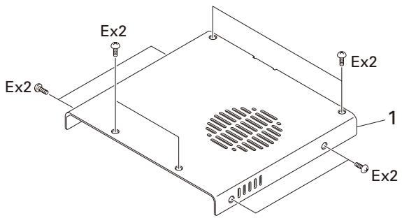
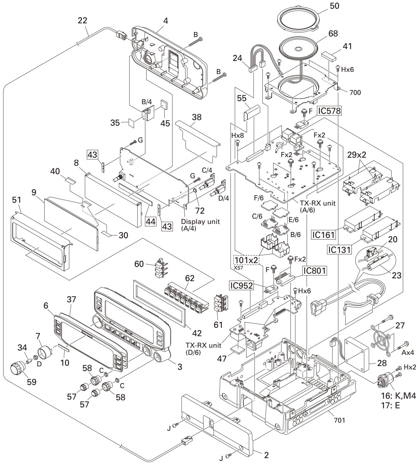
PACKING
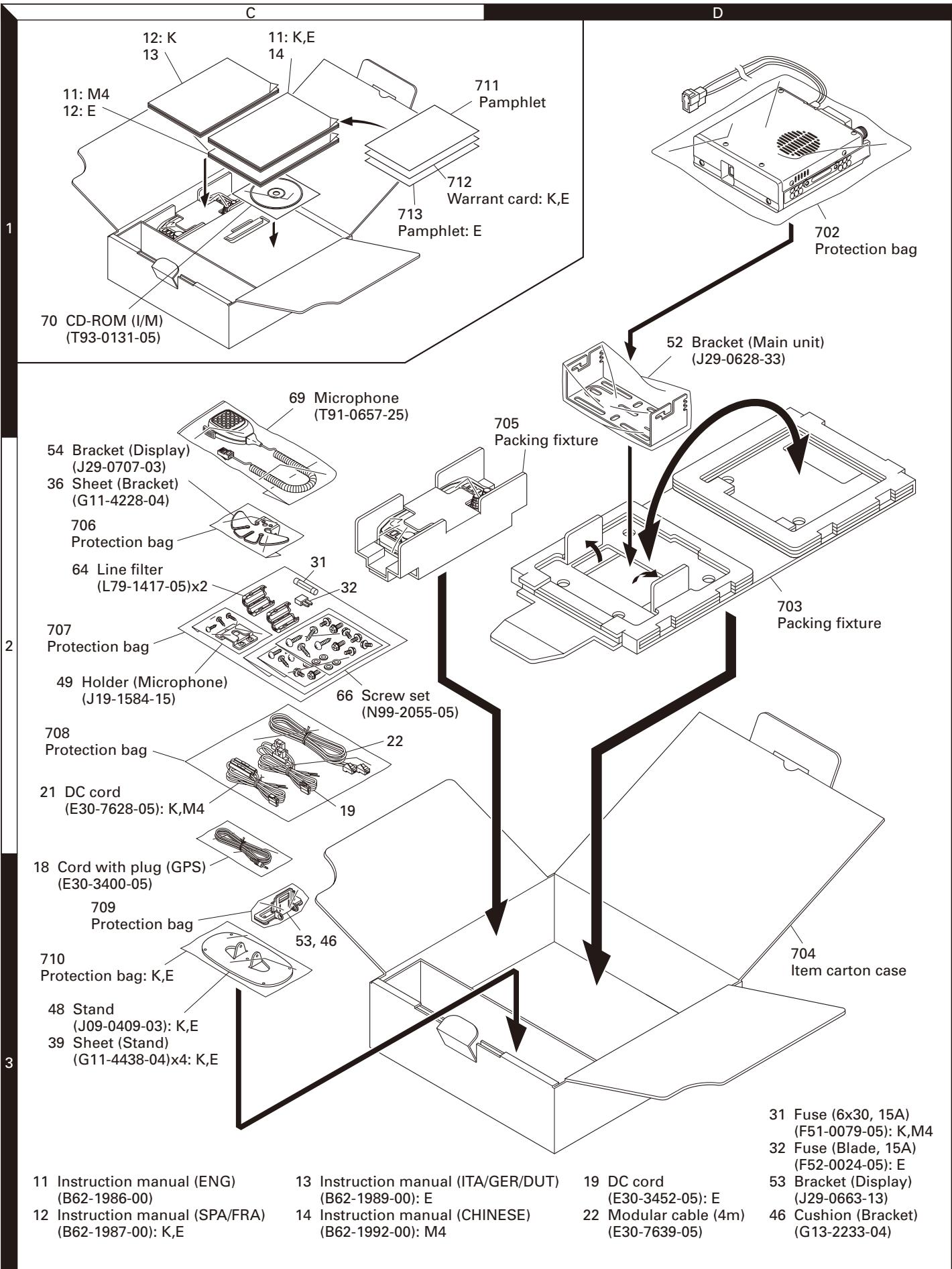
ADJUSTMENT
EchoLink Operation Check Method
You can confirm whether the terminal for EchoLink operates normally by performing the following three operation checks.
- Squelch signal operation check
- PTT signal operation check
- Voice operation check
■ Operation procedure
1) Connect the serial communications cable (8-pin mini DIN terminal and D-SUB terminal) of the PG-5H (PC interface cable kit) to the PC terminal on the rear of the transceiver.
2) Turn the transceiver power ON while pressing the [PF2] key, to enter the EchoLink Sysop mode.
3) Check the squelch signal operation.
① The squelch signal is output from pin 1 of the transceiver PC terminal or pin 8 of the PG-5H D-SUB terminal (RTS). Check the voltage of the RTS line with a digital voltmeter.
| Terminal name | PC terminal of the transceiver | D-SUB terminal of PG-5H |
| RTS | pin 1 | pin 8 |
| CTS | pin 2 | pin 7 |
PG-5H
Serial communications cable pin configuration
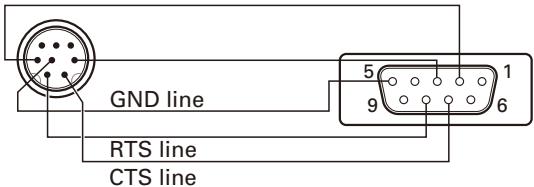
② When you open and close the transceiver squelch, check that the voltage of the RTS line increases and decreases.
(Reference voltage value of RTS line)
Voltage when squelch is closed: 10 V
Voltage when squelch is opened : -10 V
4) Check the PTT signal operation.
① Input 5 to 10 V to pin 2 of the transceiver PC terminal or pin 7 of the PG-5H D-SUB terminal (CTS).
② Ensure that the transceiver becomes the transmission state.
5) Check the voice operation.
① Connect the data communications cable (6-pin mini DIN terminal and pink/ green pin) of the PG-5H (Interface cable kit) to the DATA terminal on the rear of the transceiver.
② Input a 1kHz/ 150 mV AF signal from AG to the green pin of the data communication cable (PKD line).
Confirm the modulation of 2 to 4 kHz deviation hangs when transmitting by PTT operation as stated in step 4), above.
③ Input a standard modulation signal of -47dBm (MOD: 1kHz, DEV: 3kHz) from SSG to the transceiver.
Check that a 1kHz tone of 3 to 15 mV is output from the pink pin (PR1 line) of the data communication cable.
PG-5H
Data communications cable pin configuration
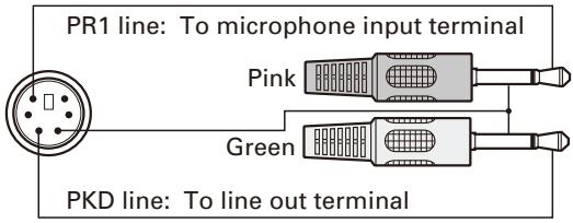
Main MPU/Panel MPU/TNC MPU Version Check Method
■ Main MPU/Panel MPU version check method
You can confirm the Main MPU and Panel MPU versions of the transceiver using its panel keys.
When confirming the version, use normal mode.
When confirming the version in APRS mode or packet mode and the beacon is transmitted, the version display is cancelled.
• Operation procedure
1) Turn the transceiver power OFF.
2) Turn the transceiver power ON while pressing the [PF1] key to enter the version display mode.
3) The Main MPU and Panel MPU versions are displayed when entering the version display mode.
4) To exit the version display mode, press the [ESC] key.
■ TNC MPU version check method
After connecting the transceiver to the PC via the PG-5G (programming cable), you can confirm the TNC MPU version by accessing the personal computer communication software.
• Operation procedure
1) Turn the transceiver power OFF.
2) Connect the RS-232C serial port of the PC to the COM terminal on the rear of the operation panel via the PG-5G (Programming cable).
3) Turn the transceiver power ON.
4) Run the personal computer communication software. The method of operating personal computer communication software "HyperTerminal" attached to Windows is described here as an example.
5) Click the "Start" button on the PC, and then select the software as follows: "Programs" → "Accessories" → "Communications" → "HyperTerminal"
TM-D710A/D710E
ADJUSTMENT
6) The HyperTerminal starts, and the "Connection Description" window is displayed.
7) Input the name that you want to use, in the "Name" column, then click "OK".
8) Change the COM Port of the "Connect using" setting if necessary. (For example, select COM1.)
9) After selecting "OK" on the "Connect To" window, the "COM1 Properties" window is displayed.
10) Confirm the PC terminal baud rate speed set to the transceiver by following these steps:
(1) Press the [F] key, then press the Tuning control.
(2) Select "AUX" by turning the Tuning control.
(3) Press the Tuning control to display the AUX menu.
(4) Turn the Tuning control to select menu number 519 (PC PORT BAUDRATE). The baud rate is displayed.
(5) Press the [ESC] key to exit menu mode.
11) Select the confirmed baud rate (from step 10, above) from the "Bits per second" pull-down menu on the "COM1 Properties" window.
12) Click "OK" on the "COM1 Properties" window. The "HyperTerminal" window is displayed.
13) Press the [TNC] key on the operation panel. "APRS 12 OPENING TNC" will appear on the display for approximately 1 second, followed by "APRS12".
Press the [TNC] key again to enter the packet mode. The TNC MPU version is displayed on the HyperTerminal window.
Kenwood Radio Modem TNC MPU version
AX.25 Level 2 Version 2.0
Release 23/Jun/07 3Chip ver1.00
cmd:DA 070702113600
cmd:
14) To exit the packet mode, press the [TNC] key.
Measuring Equipment for Alignment
- Digital voltmeter (D.V.M)
Input impedance: High -
RF valve voltmeter (RF V.M)
Input impedance: 1MΩ or more, 2pF or less
Voltage range: Full scale=10mV to 300V
Measureable frequency range: Up to 450MHz -
Frequency counter (f.counter)
Input sensitivity: About 50mV
Measureable frequency: 450MHz or more
- DC power supply
Voltage: Variable in the range 10 to 17V
Current: 13A or more
- Power meter
Measurement power: 60W, 30W, 10W
Impedance: 50Ω
Measurable frequency: 450MHz
- AF valve voltmeter (AF V.M)
Input impedance: 1MΩ or more
Voltage range: Full scale=1mV to 30V
Measurable frequency range: 50Hz to 10kHz
- AF generator (AG)
Output frequency: 100Hz to 10kHz
Output voltage: 0.5mV to 1V
- Linear detector
Measurable frequency: 450MHz
- Spectrum analyzer
Measurable frequency: 450MHz
-
Directional coupler
-
Oscilloscope
High sensitivity with horizontal input terminal
- Standard signal generator (SSG)
The standard signal generator must be able to generate the 1.3GHz band frequencies and bary the amplitude and frequency.
Output: -133dBm to greater than -13dBm
- Dummy load (for AF)
8Ω, about 5W
- Noise generator
The noise generator must be able to generate noise similar to ignition noise containing high-frequency components of 450MHz or more.
- Sweep generator
The sweep generator must be able to sweep the 144 and 430MHz bands.
- Tracking generator
ADJUSTMENT
Preparation
- To protect the signal generator, never connect the microphone to the microphone jack when the receiver section is adjusted.
- Without specification of SSG, standard modulation is applied (MOD: 1kHz, DEV: ±3kHz)
■ Operation panel (Front)
① CALL ⑩ PF1
② VFO ⑪ PF2
③ MR
⑫ SQL (Band A)
④ Tuning control ⑬ BAND SEL/ VOL (Band A)
⑤ KEY ⑭ SQL (Band B)
⑥ F
⑮ BAND SEL/ VOL (Band B)
⑦ TONE ⑯ TNC
⑧ REV ⑰ PM
⑨ LOW ⑱ Power switch
■ TX/RX unit (Rear)
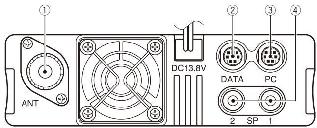
① ANT ③ PC
② DATA
④ SP (SP1/SP2)
■ Microphone jack
(as viewed from the front of the transceiver)
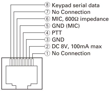
Service Jig
■ Extension flat cable (50-pin) (E37-1407-05), about 10cm to TX-RX unit (X57-731 A
to TX-RX unit (X57-731 A/6) connector (CN677)
natural_image
Simple line drawing of a curved rectangular shape with horizontal stripes (no text or symbols)to TX-RX (control section) unit (X57-731 D/6) connector (CN960)
While servicing the unit, if you are checking the foil side of the TX-RX unit (X57-731 A/6), replace the original flat cable with extension cable (E37-1407-05).
■ Data terminal short plug (W05-0611-00)
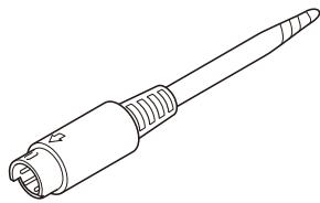
natural_image
Line drawing of a mechanical connector or connector with threaded ends and a central port (no text or symbols)Insert the adjustment jig (W05-0611-00) into the DATA connector located on the rear panel of the transceiver.

• DATA connector pin assignment
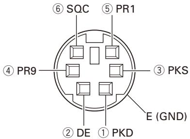
Terminals ③ and ⑥ are short circuited.
③ PKS (SEND switch for DATA terminal)
Connect PTT output. If PKS is set to "GND", data are sent and the microphone will be mute.
⑥ SQC (Squelch control output)
This outputs squelch control output.
ADJUSTMENT
Adjustment Mode
The transceiver can be adjusted using its panel keys.
■ Adjustment Items
- Frequency (Band A)
- Frequency (Band B)
- High power (144MHz band, 430MHz band)
- Mid power (144MHz band, 430MHz band)
- Low power (144MHz band, 430MHz band)
- SWR protection (144MHz band, 430MHz band)
- DCS balance (Band A) (144MHz band, 430MHz band)
- DCS balance (Band B) (144MHz band, 430MHz band)
- MAX deviation (Band A) (144MHz band, 430MHz band)
-
MAX deviation (Band B) (144MHz band, 430MHz band)
-
CTCSS deviation (Band A) (144MHz band, 430MHz band)
-
CTCSS deviation (Band B) (144MHz band, 430MHz band)
-
DCS deviation (Band A) (144MHz band, 430MHz band)
-
DCS deviation (Band B) (144MHz band, 430MHz band)
-
BPF RSSI (Band A) (144MHz band, 200MHz band, 430MHz band)*1
-
BPF RSSI (Band B) (144MHz band, 200MHz band, 430MHz band)*1
-
Squelch threshold (Band A) (144MHz band, 200MHz band, 300MHz band, 430MHz band)
-
Squelch threshold (Band B) (144MHz band, 200MHz band, 300MHz band, 430MHz band, 1.2GHz band)
-
Squelch tight (Band A) (144MHz band, 200MHz band, 300MHz band, 430MHz band)
-
Squelch tight (Band B) (144MHz band, 200MHz band, 300MHz band, 430MHz band, 1.2GHz band)
-
S-meter S1 (Band A) (144MHz band, 200MHz band, 300MHz band, 430MHz band)
-
S-meter S1 (Band B) (144MHz band, 200MHz band, 300MHz band, 430MHz band, 1.2GHz band)
-
S-meter full scale (Band A) (144MHz band, 200MHz band, 300MHz band, 430MHz band)
-
S-meter full scale (Band B) (144MHz band, 200MHz band, 300MHz band, 430MHz band, 1.2GHz band)
*1: Adjust 3 points (Low, Center, High) for the 144MHz band and the 200MHz band.
Adjust 5 points (Low, Low', Center, High', High) for the 430MHz band.
■ How to enter the adjustment mode
- Turn the transceiver power OFF and insert the data terminal short plug (W05-0611-00) into the DATA terminal located on the rear panel of the transceiver.
-
Turn the transceiver power ON while pressing the [KEY] and [F] keys to enter adjustment mode.
-
The adjustment item "FRQ A" of the Band A frequency is displayed when entering the adjustment mode.
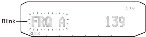
- Remove the data terminal short plug from the DATA terminal of the transceiver.
Note:
- To exit the Adjustment Mode, turn the transceiver power OFF.
- When the adjustment mode is activated, the transceiver automatically sets the frequency as shown in "The frequency that is set to the transceiver" table, on pages 36 to 38.
■ LCD display in the adjustment mode
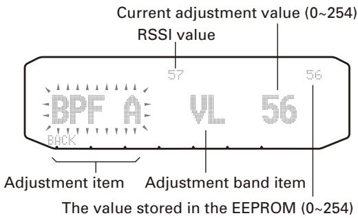
■ Panel key operation in the adjustment mode
| Key name | Function | |
| Tuning control | (Turn) | Changes the adjustment item or adjustment band item.Increase or decrease the adjustment values (0~254). |
| (Press) | Movement from the adjustment item display to the adjustment band item display or movement from the adjustment band item display to the adjustment value dispaly. (Forward)Write adjustment values. | |
| [CALL], [BACK] | Movement from the adjustment value display to the adjustment band item display or movement from the adjustment band item display to the adjustment item display. (Back) | |
| [VFO],[MR],[F],[TONE],[REV],[LOW],[PF1],[PF2],[TNC],[PM] | Unused | |
| Microphone key | ||
| [PTT] | Transmit. (Only the adjustment item of the transmitter section can be used.) | |
ADJUSTMENT
■ Example of the adjustment mode operation procedure
The operating procedure when the BPF RSSI of band A (430MHz band, low frequency) is adjusted is described as follows.
The adjustment item "FRQ A" of the band A frequency is displayed when entering the adjustment mode according to the operating procedure of "How to enter the adjustment mode" described on page 34.
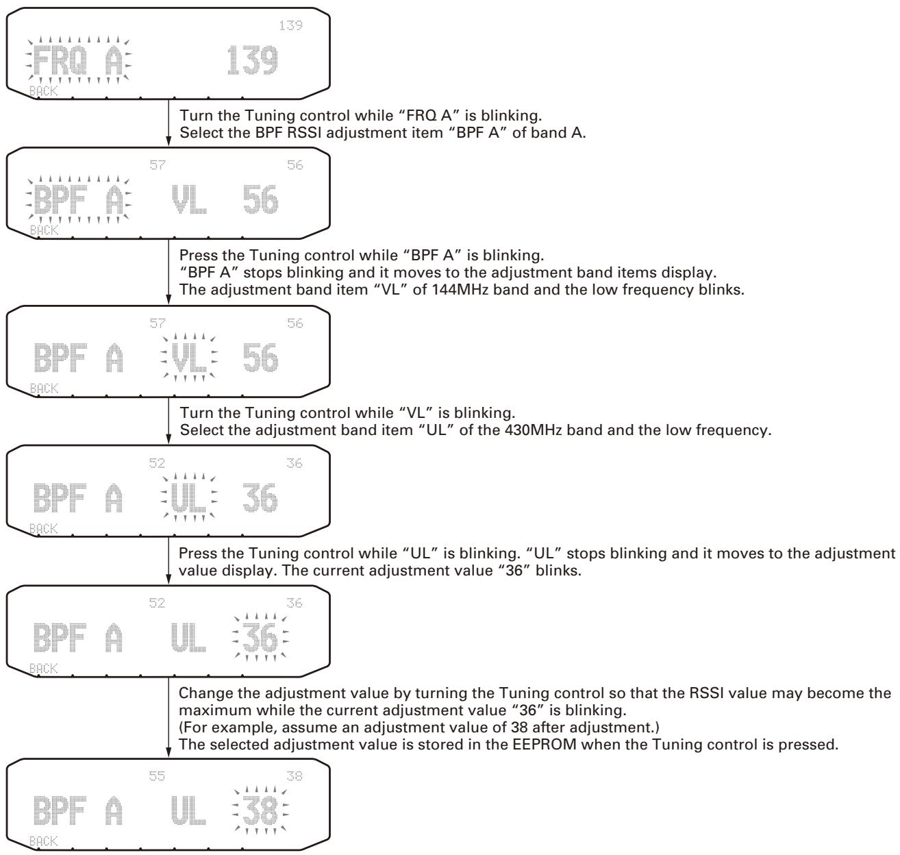
flowchart
graph TD
    A["FRQ A 139"] -->|Turn the Tuning control while "FRQ A" is blinking. Select the BPF RSSI adjustment item "BPF A" of band A.| B["BPF A 57 VL 56"]
    B -->|Press the Tuning control while "BPF A" is blinking. "BPF A" stops blinking and it moves to the adjustment band items display. The adjustment band item "VL" of 144MHz band and the low frequency blinks.| C["BPF A 57 VL 56"]
    C -->|Turn the Tuning control while "VL" is blinking. Select the adjustment band item "UL" of the 430MHz band and the low frequency.| D["BPF A 52 UL 36"]
    D -->|Press the Tuning control while "UL" is blinking. "UL" stops blinking and it moves to the adjustment value display. The current adjustment value "36" blinks.| E["BPF A 52 UL 36"]
    E -->|Change the adjustment value by turning the Tuning control so that the RSSI value may become the maximum while the current adjustment value "36" is blinking. (For example, assume an adjustment value of 38 after adjustment.) | F["BPF A 55 UL 38"]
    F -->|The selected adjustment value is stored in the EEPROM when the Tuning control is pressed.| G["Back"]
ADJUSTMENT
■ Adjustment item, adjustment band item, display and the frequency that is set to the transceiver
| No. | Adjustment item | Adjustment band item | Display | The frequency that is set to the transceiver | Signaling | ||
| Adjustment item | Adjustment band item | K type | E, M4 types | ||||
| 1 | Frequency (Band A) | - | FRQ A | - | 444.100MHz | 435.100MHz | |
| 2 | Frequency (Band B) | - | FRQ B | - | 444.100MHz | 435.100MHz | |
| 3 | High power | 144MHz band | HPWR | V | 146.100MHz | 145.100MHz | |
| 430MHz band | HPWR | U | 444.100MHz | 435.100MHz | |||
| 4 | Mid power | 144MHz band | MPWR | V | 146.100MHz | 145.100MHz | |
| 430MHz band | MPWR | U | 444.100MHz | 435.100MHz | |||
| 5 | Low power | 144MHz band | LPWR | V | 146.100MHz | 145.100MHz | |
| 430MHz band | LPWR | U | 444.100MHz | 435.100MHz | |||
| 6 | SWR protection | 144MHz band | SWR | V | 146.100MHz | 145.100MHz | |
| 430MHz band | SWR | U | 444.100MHz | 435.100MHz | |||
| 7 | DCS balance *1(Band A) | 144MHz band, Low frequency | BAL A | VL | 136.100MHz | 136.100MHz | |
| 144MHz band, Center frequency | BAL A | VC | 146.100MHz | 145.100MHz | |||
| 144MHz band, High frequency | BAL A | VH | 173.900MHz | 173.900MHz | |||
| 430MHz band, Low frequency | BAL A | UL | 400.100MHz | 400.100MHz | |||
| 430MHz band, Center frequency | BAL A | UC | 444.100MHz | 435.100MHz | |||
| 430MHz band, High frequency | BAL A | UH | 469.900MHz | 469.900MHz | |||
| 8 | DCS balance *1(Band B) | 144MHz band, Low frequency | BAL B | VL | 136.100MHz | 136.100MHz | |
| 144MHz band, Center frequency | BAL B | VC | 146.100MHz | 145.100MHz | |||
| 144MHz band, High frequency | BAL B | VH | 173.900MHz | 173.900MHz | |||
| 430MHz band, Low frequency | BAL B | UL | 400.100MHz | 400.100MHz | |||
| 430MHz band, Center frequency | BAL B | UC | 444.100MHz | 435.100MHz | |||
| 430MHz band, High frequency | BAL B | UH | 469.900MHz | 469.900MHz | |||
| 9 | MAX deviation(Band A) | 144MHz band | DEV A | V | 146.100MHz | 145.100MHz | |
| 430MHz band | DEV A | U | 444.100MHz | 435.100MHz | |||
| 10 | MAX deviation(Band B) | 144MHz band | DEV B | V | 146.100MHz | 145.100MHz | |
| 430MHz band | DEV B | U | 444.100MHz | 435.100MHz | |||
| 11 | CTCSS deviation(Band A) | 144MHz band | CT A | V | 146.100MHz | 145.100MHz | CTCSS: 91.5Hz |
| 430MHz band | CT A | U | 444.100MHz | 435.100MHz | |||
| 12 | CTCSS deviation(Band B) | 144MHz band | CT B | V | 146.100MHz | 145.100MHz | CTCSS: 91.5Hz |
| 430MHz band | CT B | U | 444.100MHz | 435.100MHz | |||
| 13 | DCS deviation(Band A) | 144MHz band | DCS A | V | 146.100MHz | 145.100MHz | DCS: 023 |
| 430MHz band | DCS A | U | 444.100MHz | 435.100MHz | |||
| 14 | DCS deviation(Band B) | 144MHz band | DCS B | V | 146.100MHz | 145.100MHz | DCS: 023 |
| 430MHz band | DCS B | U | 444.100MHz | 435.100MHz | |||
*1: The DCS balance adjustment can adjust only the center frequency.
ADJUSTMENT
| No. | Adjustment item | Adjustment band item | Display | The frequency that is set to the transceiver | Signaling | ||
| Adjustment item | Adjustment band item | K type | E, M4 types | ||||
| 15 | BPF RSSI (Band A) | 144MHz band, Low frequency | BPF A | VL | 118.050MHz | 118.050MHz | |
| 144MHz band, Center frequency | BPF A | VC | 145.050MHz | 145.050MHz | |||
| 144MHz band, High frequency | BPF A | VH | 199.950MHz | 199.950MHz | |||
| 200MHz band, Low frequency | BPF A | 2L | 220.050MHz | 220.050MHz | |||
| 200MHz band, Center frequency | BPF A | 2C | 250.050MHz | 250.050MHz | |||
| 200MHz band, High frequency | BPF A | 2H | 279.950MHz | 279.950MHz | |||
| 430MHz band, Low frequency | BPF A | UL | 300.050MHz | 300.050MHz | |||
| 430MHz band, Low' frequency | BPF A | ULD | 350.050MHz | 350.050MHz | |||
| 430MHz band, Center frequency | BPF A | UC | 400.050MHz | 400.050MHz | |||
| 430MHz band, High' frequency | BPF A | UHD | 440.050MHz | 440.050MHz | |||
| 430MHz band, High frequency | BPF A | UH | 500.050MHz | 500.050MHz | |||
| 16 | BPF RSSI (Band B) | 144MHz band, Low frequency | BPF B | VL | 118.050MHz | 118.050MHz | |
| 144MHz band, Center frequency | BPF B | VC | 145.050MHz | 145.050MHz | |||
| 144MHz band, High frequency | BPF B | VH | 199.950MHz | 199.950MHz | |||
| 200MHz band, Low frequency | BPF B | 2L | 220.050MHz | 220.050MHz | |||
| 200MHz band, Center frequency | BPF B | 2C | 250.050MHz | 250.050MHz | |||
| 200MHz band, High frequency | BPF B | 2H | 279.950MHz | 279.950MHz | |||
| 430MHz band, Low frequency | BPF B | UL | 300.050MHz | 300.050MHz | |||
| 430MHz band, Low' frequency | BPF B | ULD | 350.050MHz | 350.050MHz | |||
| 430MHz band, Center frequency | BPF B | UC | 400.050MHz | 400.050MHz | |||
| 430MHz band, High' frequency | BPF B | UHD | 440.050MHz | 440.050MHz | |||
| 430MHz band, High frequency | BPF B | UH | 500.050MHz | 500.050MHz | |||
| 17 | Squelch threshold (Band A) | 144MHz band | SQ1 A | V | 145.050MHz | 145.050MHz | |
| 200MHz band | SQ1 A | 2 | 220.050MHz | 220.050MHz | |||
| 300MHz band | SQ1 A | 3 | 350.050MHz | 350.050MHz | |||
| 430MHz band | SQ1 A | U | 440.050MHz | 440.050MHz | |||
| 18 | Squelch threshold (Band B) | 144MHz band | SQ1 B | V | 145.050MHz | 145.050MHz | |
| 200MHz band | SQ1 B | 2 | 220.050MHz | 220.050MHz | |||
| 300MHz band | SQ1 B | 3 | 350.050MHz | 350.050MHz | |||
| 430MHz band | SQ1 B | U | 440.050MHz | 440.050MHz | |||
| 1.2GHz band | SQ1 B | 8 | 1270.050MHz | 1270.050MHz | |||
| 19 | Squelch tight (Band A) | 144MHz band | SQT A | V | 145.050MHz | 145.050MHz | |
| 200MHz band | SQT A | 2 | 220.050MHz | 220.050MHz | |||
| 300MHz band | SQT A | 3 | 350.050MHz | 350.050MHz | |||
| 430MHz band | SQT A | U | 440.050MHz | 440.050MHz | |||
ADJUSTMENT
| No. | Adjustment item | Adjustment band item | Display | The frequency that is set to the transceiver | Signaling | ||
| Adjustment item | Adjustment band item | K type | E, M4 types | ||||
| 20 | Squelch tight (Band B) | 144MHz band | SQT B | V | 145.050MHz | 145.050MHz | |
| 200MHz band | SQT B | 2 | 220.050MHz | 220.050MHz | |||
| 300MHz band | SQT B | 3 | 350.050MHz | 350.050MHz | |||
| 430MHz band | SQT B | U | 440.050MHz | 440.050MHz | |||
| 1.2GHz band | SQT B | 8 | 1270.050MHz | 1270.050MHz | |||
| 21 | S-meter S1 (Band A) | 144MHz band | SM1 A | V | 145.050MHz | 145.050MHz | |
| 200MHz band | SM1 A | 2 | 220.050MHz | 220.050MHz | |||
| 300MHz band | SM1 A | 3 | 350.050MHz | 350.050MHz | |||
| 430MHz band | SM1 A | U | 440.050MHz | 440.050MHz | |||
| 22 | S-meter S1 (Band B) | 144MHz band | SM1 B | V | 145.050MHz | 145.050MHz | |
| 200MHz band | SM1 B | 2 | 220.050MHz | 220.050MHz | |||
| 300MHz band | SM1 B | 3 | 350.050MHz | 350.050MHz | |||
| 430MHz band | SM1 B | U | 440.050MHz | 440.050MHz | |||
| 1.2GHz band | SM1 B | 8 | 1270.050MHz | 1270.050MHz | |||
| 23 | S-meter full scale (Band A) | 144MHz band | SM7 A | V | 145.050MHz | 145.050MHz | |
| 200MHz band | SM7 A | 2 | 220.050MHz | 220.050MHz | |||
| 300MHz band | SM7 A | 3 | 350.050MHz | 350.050MHz | |||
| 430MHz band | SM7 A | U | 440.050MHz | 440.050MHz | |||
| 24 | S-meter full scale (Band B) | 144MHz band | SM7 B | V | 145.050MHz | 145.050MHz | |
| 200MHz band | SM7 B | 2 | 220.050MHz | 220.050MHz | |||
| 300MHz band | SM7 B | 3 | 350.050MHz | 350.050MHz | |||
| 430MHz band | SM7 B | U | 440.050MHz | 440.050MHz | |||
| 1.2GHz band | SM7 B | 8 | 1270.050MHz | 1270.050MHz | |||
ADJUSTMENT
Common Section
| Item | Condition | Measurement | Adjustment | Specifications / Remarks | ||||
| Test-equipment | Unit | Terminal | Unit | Parts | Method | |||
| 1.Setting | 1) Power supply voltageDC power supply terminal: 13.8V | |||||||
| 2. Full reset | 1) Full resetTurn the transceiver power ON by pressing the power switch while [F] key is pressed. Release the [F] key.Select reset type "FULL RESET" by tuning the Tuning control when the reset confirmation message appears.Press the Tuning control to set the reset type.Press the Tuning control again to perform the full reset.* This adjustment mode has an adjustment item to be used as is in the user mode setting contents (AIP, menu mode, etc).Therefore, if you do not perform the full reset, it may be adjusted unintentionally.Note:When you do not want to remove data such as memory channel data, save the data using the MCP-2A (Memory control program) before performing the full reset, then write the data to the transceiver after performing the adjustment. | |||||||
Transmitter Section: Adjustment Mode Setting Items
(Refer to the table on pages 36 to 38 for the frequencies which will apply in the adjustment mode.)
| Item | Condition | Measurement | Adjustment | Specifications / Remarks | ||||
| Test-equipment | Unit | Terminal | Unit | Parts | Method | |||
| 1. Frequency (Band A) Adjust | 1) Adj item: [FRQ A] Adjust: [***] 2) PTT: ON | f. counter | TX/RX unit (Rear) | ANT | Operation panel (Front) | Tuning control | Write | 435.100MHz±100Hz E,M4 444.100MHz±100Hz K |
| 2. Frequency (Band B) Adjust | 1) Adj item: [FRQ B] Adjust: [***] 2) PTT: ON | |||||||
| 3. High power Adjust• 144MHz band | 1) Adj item: [HPWR V] Adjust: [***] 2) PTT: ON | Power meter | Write | 50W±1W | ||||
| • 430MHz band | 3) Adj item: [HPWR U] Adjust: [***] 4) PTT: ON | 48W±1W | ||||||
| 4. Mid power Adjust• 144MHz band | 1) Adj item: [MPWR V] Adjust: [***] 2) PTT: ON | Write | 12W±1W K,E 22.5W±1W M4 | |||||
| • 430MHz band | 3) Adj item: [MPWR U] Adjust: [***] 4) PTT: ON | |||||||
| 5. Low power Adjust• 144MHz band | 1) Adj item: [LPWR V] Adjust: [***] 2) PTT: ON | Write | 5W±1W | |||||
| • 430MHz band | 3) Adj item: [LPWR U] Adjust: [***] 4) PTT: ON | |||||||
ADJUSTMENT
| Item | Condition | Measurement | Adjustment | Specifications / Remarks | ||||
| Test-equipment | Unit | Terminal | Unit | Parts | Method | |||
| 6. SWR protection Adjust• 144MHz band | 1) Adj item: [SWR V]Adjust: [***]2) PTT: ON | Power meter | TX/RX unit (Rear) | ANT | Operation panel (Front) | Tuning control | Set the following adjustment values to the transceiver by turning the Tuning control.* When the transceiver is shipped, the SWR adjustment value is different from that which is stated in this manual, as SWR protection adjustment is performed at production.Although there is a difference in the numerical value, this does not pose a problem, as the adjustment value provided in this manual is the mean value.Adjustment value: 66 | |
| Note:Do not usually adjust the SWR protection adjustment; adjust it only when you replace the EEPROM. | ||||||||
| • 430MHz band | 3) Adj item: [SWR U]Adjust: [***]4) PTT: ON | Adjustment value: 120 | ||||||
| 7. DCS balance (Band A)Adjust• 144MHz band | 1) Adj item: [BAL A VC]Adjust: [***]Detector: +P HOLDLPF: 3kHzHPF: OFFDe-emphasis: OFF2) PTT: ON | Linear detectorOscilloscope | By turning the Tuning control, adjust the modulation wave until it becomes the square wave. |  | ||||
| • 430MHz band | 3) Adj item: [BAL A UC]Adjust: [***]4) PTT: ON | |||||||
| 8. DCS balance (Band B)Adjust• 144MHz band | 1) Adj item: [BAL B VC]Adjust: [***]Detector: +P HOLDLPF: 3kHzHPF: OFFDe-emphasis: OFF2) PTT: ON | |||||||
| • 430MHz band | 3) Adj item: [BAL B UC]Adjust: [***]4) PTT: ON | |||||||
| 9. MAX deviation (Band A)Adjust• 144MHz band | 1) Adj item: [DEV A V]Adjust: [***]AG: 1kHz/50mV K,M4AG: 1kHz/20mVE Detector: +P, -PLPF: 15kHzHPF: OFFDe-emphasis: OFF2) PTT: ON | Linear detectorOscilloscopeAGAF V.M | ANTMIC | Write | 4.2kHz±0.1kHz (According to the larger +P, -P) | |||
| • 430MHz band | 3) Adj item: [DEV A U]Adjust: [***]4) PTT: ON | |||||||
| 10. MAX deviation (Band B)Adjust• 144MHz band | 1) Adj item: [DEV B V]Adjust: [***]AG: 1kHz/50mV K,M4AG: 1kHz/20mVE Detector: +P, -PLPF: 15kHzHPF: OFFDe-emphasis: OFF2) PTT: ON | |||||||
| • 430MHz band | 3) Adj item: [DEV B U]Adjust: [***]4) PTT: ON | |||||||
ADJUSTMENT
| Item | Condition | Measurement | Adjustment | Specifications / Remarks | ||||
| Test-equipment | Unit | Terminal | Unit | Parts | Method | |||
| 11. CTCSS deviation (Band A) Adjust• 144MHz band | 1) Adj item: [CT A V]Adjust: [***]Detector: P-P/2LPF: 3kHzHPF: OFFDe-emphasis: OFFPTT:ON | Linear detector Oscilloscope | TX/RX unit (Rear) | ANT | Operation panel (Front) | Tuning control | Write | 0.75kHz±0.05kHz |
| • 430MHz band | 2) Adj item: [CT A U]Adjust: [***]PTT: ON | |||||||
| 12. CTCSS deviation (Band B) Adjust• 144MHz band | 1) Adj item: [CT B V]Adjust: [***]Detector: P-P/2LPF: 3kHzHPF: OFFDe-emphasis: OFFPTT: ON | |||||||
| • 430MHz band | 2) Adj item: [CT B U]Adjust: [***]PTT: ON | |||||||
| 13. DCS deviation (Band A) Adjust• 144MHz band | 1) Adj item: [DCS A V]Adjust: [***]Detector: +P HOLDLPF: 3kHzHPF: OFFDe-emphasis: OFFPTT: ON | Write | 0.75kHz±0.05kHz | |||||
| • 430MHz band | 2) Adj item: [DCS A V]Adjust: [***]PTT: ON | |||||||
| 14. DCS deviation (Band B) Adjust• 144MHz band | 1) Adj item: [DCS B V]Adjust: [***]Detector: +P HOLDLPF: 3kHzHPF: OFFDe-emphasis: OFFPTT: ON | |||||||
| • 430MHz band | 2) Adj item: [DCS B U]Adjust: [***]PTT: ON | |||||||
Transmitter Section: User Mode Confirmation Items
(Do not insert the data terminal short plug to the DATA terminal of the transceiver when entering user mode.)
| Item | Condition | Measurement | Adjustment | Specifications / Remarks | ||||
| Test-equipment | Unit | Terminal | Unit | Parts | Method | |||
| 1. High power Check• Band A | 1) Frequency: 144.000MHz2) Frequency: 145.990MHz EFrequency: 147.990MHz K3) PTT: ON | Power meter Ammeter | TX/RX unit (Rear) | ANT | Check | 47~53W12A or less | ||
| 4) Frequency: 430.000MHz EFrequency: 438.000MHz K5) Frequency: 435.000MHz EFrequency: 444.000MHz K6) Frequency: 439.990MHz EFrequency: 449.990MHz K7) PTT: ON | 45~51W12A or less | |||||||
ADJUSTMENT
| Item | Condition | Measurement | Adjustment | Specifications / Remarks | ||||
| Test-equipment | Unit | Terminal | Unit | Parts | Method | |||
| • Band B | 8) Frequency: 144.000MHz9) Frequency: 145.000MHz EFrequency: 146.000MHz K10) Frequency: 145.990MHz EFrequency: 147.990MHz K11) PTT: ON | Power meter Ammeter | TX/RX unit (Rear) | ANT | Check | 47~53W12A or less | ||
| 12) Frequency: 430.000MHz EFrequency: 438.000MHz K13) Frequency: 439.990MHz EFrequency: 449.990MHz K14) PTT: ON | 45~51W12A or less | |||||||
| 2. Mid power Check• Band A | 1) Frequency: 144.000MHz2) Frequency: 145.990MHz E,M4Frequency: 147.990MHz K3) PTT: ON | Check | K,E: 11~13W, 5A or lessM4: 20.5~24.5W, 8A or less | |||||
| 4) Frequency: 430.000MHz E,M4Frequency: 438.000MHz K5) Frequency: 435.000MHz E,M4Frequency: 444.000MHz K6) Frequency: 439.990MHz E,M4Frequency: 449.990MHz K7) PTT: ON | K,E: 11~13W, 6A or lessM4: 20.5~24.5W, 8A or less | |||||||
| • Band B | 8) Frequency: 144.000MHz9) Frequency: 145.000MHz E,M4Frequency: 146.000MHz K10) Frequency: 145.990MHz E,M4Frequency: 147.990MHz K11) PTT: ON | Check | K,E: 11~13W, 5A or lessM4: 20.5~24.5W, 8A or less | |||||
| 12) Frequency: 430.000MHz E,M4Frequency: 438.000MHz K13) Frequency: 439.990MHz E,M4Frequency: 449.990MHz K14) PTT: ON | K,E: 11~13W, 6A or lessM4: 20.5~24.5W, 8A or less | |||||||
| 3. Low power Check• Band A | 1) Frequency: 144.000MHz2) Frequency: 145.990MHz E,M4Frequency: 147.990MHz K3) PTT: ON | Check | 4~6W3.5A or less | |||||
| 4) Frequency: 430.000MHz E,M4Frequency: 438.000MHz K5) Frequency: 435.000MHz E,M4Frequency: 444.000MHz K6) Frequency: 439.990MHz E,M4Frequency: 449.990MHz K7) PTT: ON | 4~6W4.5A or less | |||||||
| • Band B | 8) Frequency: 144.000MHz9) Frequency: 145.000MHz E,M4Frequency: 146.000MHz K10) Frequency: 145.990MHz E,M4Frequency: 147.990MHz K11) PTT: ON | Check | 4~6W3.5A or less | |||||
| 12) Frequency: 430.000MHz E,M4Frequency: 438.000MHz K13) Frequency: 439.990MHz E,M4Frequency: 449.990MHz K14) PTT: ON | 4~6W4.5A or less | |||||||
ADJUSTMENT
| Item | Condition | Measurement | Adjustment | Specifications / Remarks | ||||
| Test-equipment | Unit | Terminal | Unit | Parts | Method | |||
| 4. MIC sensitivity Check• Band A | 1) Frequency: 145.000MHz E,M4Frequency: 146.000MHz KAG: 1kHz/5mV K,M4AG: 1kHz/2mV EDetector: P-P/2LPF: 15kHzHPF: OFFDe-emphasis: OFF2) PTT: ON | Linear detector Oscilloscope AGAF V.M | TX/RX unit (Rear) | ANTMIC | Check | ±2.34~4.17kHz K,M4±2.38~4.05kHz E | ||
| 3) Frequency: 435.000MHz E,M4Frequency: 444.000MHz K4) PTT: ON | ||||||||
| • Band B | 5) Frequency: 145.000MHz E,M4Frequency: 146.000MHz KAG: 1kHz/5mV K,M4AG: 1kHz/2mV EDetector: P-P/2LPF: 15kHzHPF: OFFDe-emphasis: OFF6) PTT: ON | Check | ±2.34~4.17kHz K,M4±2.38~4.05kHz E | |||||
| 7) Frequency: 435.000MHz E,M4Frequency: 444.000MHz K8) PTT: ON | ||||||||
| 5. CTCSS deviation Check• Band A | 1) Frequency: 145.000MHz E,M4Frequency: 146.000MHz KDetector: P-P/2LPF: 3kHzHPF: OFFDe-emphasis: OFF2) PTT: ON | Linear detector Oscilloscope | ANT | Check | 0.65~0.85kHz | |||
| 3) Frequency: 435.000MHz E,M4Frequency: 444.000MHz K4) PTT: ON | ||||||||
| • Band B | 5) Frequency: 145.000MHz E,M4Frequency: 146.000MHz KDetector: P-P/2LPF: 3kHzHPF: OFFDe-emphasis: OFF6) PTT: ON | |||||||
| 7) Frequency: 435.000MHz E,M4Frequency: 444.000MHz K8) PTT: ON | ||||||||
| 6. DCS deviation Check• Band A | 1) Frequency: 145.000MHz E,M4Frequency: 146.000MHz KDetector: +P HOLDLPF: 3kHzHPF: OFFDe-emphasis: OFF2) PTT: ON | Check | 0.65~0.85kHz | |||||
| 3) Frequency: 435.000MHz E,M4Frequency: 444.000MHz K4) PTT: ON | ||||||||
ADJUSTMENT
| Item | Condition | Measurement | Adjustment | Specifications / Remarks | ||||
| Test-equipment | Unit | Terminal | Unit | Parts | Method | |||
| • Band B | 5) Frequency: 145.000MHz E,M4Frequency: 146.000MHz KDetector: +P HOLDLPF: 3kHzHPF: OFFDe-emphasis: OFF6) PTT: ON | Linear detectorOscilloscope | TX/RX unit(Rear) | ANT | Check | 0.65~0.85kHz | ||
| 7) Frequency: 435.000MHz E,M4Frequency: 444.000MHz K8) PTT: ON | ||||||||
| 7 .Protection Check• Band A | TX Power: High K,EMid M4ANT: Short circuit and Open1) Frequency: 145.000MHz E,M4Frequency: 146.000MHz K2) PTT: ON | Ammeter | Check | 12A or less | ||||
| • Band B | 3) Frequency: 435.000MHz E,M4Frequency: 444.000MHz K4) PTT: ON | |||||||
Receiver Section: Adjustment Mode Setting Items
(Refer to the table on pages 36 to 38 for the frequencies which will apply in the adjustment mode.)
| Item | Condition | Measurement | Adjustment | Specifications / Remarks | ||||
| Test-equipment | Unit | Terminal | Unit | Parts | Method | |||
| 1. BPF RSSI(Band A)Adjust• 144MHz band | 1) Adj item: [BPF A VL] →[BPF A VC] → [BPF A VH]Adjust: [***]SSG output: -100dBm (2.24μV)SSG MOD: 1kHzSSG DEV: 3kHz | SSG Oscilloscope Distortion meterAF V.M Dummy load | TX/RX unit (Rear) | ANT EXT.SP | Operation panel (Front) | Tuning control | Turn the Tuning control until the maximum RSSI value will appear on the LCD. When the same RSSI value remains while it is being adjusted, set the adjustment value to the center value.For example, set the adjustment value to 38 for the values listed below. | |
| • 200MHz band | 2) Adj item: [BPF A 2L]Adjust: [***]SSG output: -100dBm (2.24μV)3) Adj item: [BPF A 2C]Adjust: [***]SSG output: -90dBm (7.08μV)4) Adj item: [BPF A 2H]Adjust: [***]SSG output: -80dBm (22.4μV) | |||||||
| • 430MHz band | 5) Adj item: [BPF A UL]Adjust: [***]SSG output: -90dBm (7.08μV)6) Adj item: [BPF A ULD] →[BPF A UC] → [BPF A UHD]→ [BPF A UH]Adjust: [***]SSG output: -100dBm (2.24μV) | RSSI value | Adjustment value | |||||
| 54 | 35 | |||||||
| 55 | 36 | |||||||
| 55 | 37 | |||||||
| 55 | 38 | |||||||
| 55 | 39 | |||||||
| 55 | 40 | |||||||
| 54 | 41 | |||||||
ADJUSTMENT
| Item | Condition | Measurement | Adjustment | Specifications / Remarks | ||||
| Test-equipment | Unit | Terminal | Unit | Parts | Method | |||
| 2. BPF RSSI (Band B) Adjust• 144MHz band | 1) Adj item: [BPF B VL] → [BPF B VC] → [BPF B VH]Adjust: [***]SSG output: -100dBm (2.24μV)SSG MOD: 1kHzSSG DEV: 3kHz | SSG Oscilloscope Distortion meter AF V.M Dummy load | TX/RX unit (Rear) | ANT EXT.SP | Operation panel (Front) | Tuning control | Turn the Tuning control until the maximum RSSI value will appear on the LCD. When the same RSSI value remains while it is being adjusted, set the adjustment value to the center value.For example, set the adjustment value to 38 for the values listed below. | |
| • 200MHz band | 2) Adj item: [BPF B 2L]Adjust: [***]SSG output: -100dBm (2.24μV)3) Adj item: [BPF B 2C]Adjust: [***]SSG output: -90dBm (7.08μV)4) Adj item: [BPF B 2H]Adjust: [***]SSG output: -80dBm (22.4μV) | |||||||
| • 430MHz band | 5) Adj item: [BPF B UL]Adjust: [***]SSG output: -90dBm (7.08μV)6) Adj item: [BPF B ULD] → [BPF A UC] → [BPF A UHD] → [BPF A UH]Adjust: [***]SSG output: -100dBm (2.24μV) | RSSI value | Adjustment value | |||||
| 54 | 35 | |||||||
| 55 | 36 | |||||||
| 55 | 37 | |||||||
| 55 | 38 | |||||||
| 55 | 39 | |||||||
| 55 | 40 | |||||||
| 54 | 41 | |||||||
| 3. Squelch threshold (Band A) Writing• 144MHz band | 1) Adj item: [SQ1 A V]Adjust: [***]SSG output: -128dBm (0.089μV)SSG MOD: 1kHzSSG DEV: 3kHz | SSG | ANT | Write | ||||
| • 200MHz band | 2) Adj item: [SQ1 A 2]Adjust: [***]SSG output: -117dBm (0.32μV) | |||||||
| • 300MHz band | 3) Adj item: [SQ1 A 3]Adjust: [***]SSG output: -117dBm (0.32μV) | |||||||
| • 430MHz band | 4) Adj item: [SQ1 A U]Adjust: [***]SSG output: -128dBm (0.089μV) | |||||||
| 4. Squelch threshold (Band B) Writing• 144MHz band | 1) Adj item: [SQ1 B V]Adjust: [***]SSG output: -128dBm (0.089μV)SSG MOD: 1kHzSSG DEV: 3kHz | |||||||
| • 200MHz band | 2) Adj item: [SQ1 B 2]Adjust: [***]SSG output: -117dBm (0.32μV) | |||||||
| • 300MHz band | 3) Adj item: [SQ1 B 3]Adjust: [***]SSG output: -117dBm (0.32μV) | |||||||
| • 430MHz band | 4) Adj item: [SQ1 B U]Adjust: [***]SSG output: -128dBm (0.089μV) | |||||||
| • 1.2GHz band | 5) Adj item: [SQ1 B 8]Adjust: [***]SSG output: -108dBm (0.89μV) | |||||||
ADJUSTMENT
| Item | Condition | Measurement | Adjustment | Specifications / Remarks | ||||
| Test-equipment | Unit | Terminal | Unit | Parts | Method | |||
| 5. Squelchtight(Band A)Writing• 144MHz band | 1) Adj item: [SQT A V]Adjust: [***]SSG output: -119dBm (0.25μV)SSG MOD: 1kHzSSG DEV: 3kHz | SSG | TX/RX unit(Rear) | ANT | Operation panel(Front) | Tuning control | Write | |
| • 200MHz band | 2) Adj item: [SQT A 2]Adjust: [***]SSG output: -108dBm (0.89μV) | |||||||
| • 300MHz band | 3) Adj item: [SQT A 3]Adjust: [***]SSG output: -108dBm (0.89μV) | |||||||
| • 430MHz band | 4) Adj item: [SQT A U]Adjust: [***]SSG output: -119dBm (0.25μV) | |||||||
| 6. Squelchtight(Band B)Writing• 144MHz band | 1) Adj item: [SQT B V]Adjust: [***]SSG output: -119dBm (0.25μV)SSG MOD: 1kHzSSG DEV: 3kHz | |||||||
| • 200MHz band | 2) Adj item: [SQT B 2]Adjust: [***]SSG output: -108dBm (0.89μV) | |||||||
| • 300MHz band | 3) Adj item: [SQT B 3]Adjust: [***]SSG output: -108dBm (0.89μV) | |||||||
| • 430MHz band | 4) Adj item: [SQT B U]Adjust: [***]SSG output: -119dBm (0.25μV) | |||||||
| • 1.2GHz band | 5) Adj item: [SQT B 8]Adjust: [***]SSG output: -98dBm (2.82μV) | |||||||
| 7. S-meter S1(Band A)Writing• 144MHz band | 1) Adj item: [SM1 A V]Adjust: [***]SSG output: -118dBm (0.28μV)SSG MOD: 1kHzSSG DEV: 3kHz | |||||||
| • 200MHz band | 2) Adj item: [SM1 A 2]Adjust: [***]SSG output: -108dBm (0.89μV) | |||||||
| • 300MHz band | 3) Adj item: [SM1 A 3]Adjust: [***]SSG output: -108dBm (0.89μV) | |||||||
| • 430MHz band | 4) Adj item: [SM1 A U]Adjust: [***]SSG output: -118dBm (0.28μV) | |||||||
ADJUSTMENT
| Item | Condition | Measurement | Adjustment | Specifications / Remarks | ||||
| Test-equipment | Unit | Terminal | Unit | Parts | Method | |||
| 8 .S-meter S1 (Band B) Writing• 144MHz band | 1) Adj item: [SM1 B V]Adjust: [***]SSG output: -118dBm (0.28μV)SSG MOD: 1kHzSSG DEV: 3kHz | SSG | TX/RX unit (Rear) | ANT | Operation panel (Front) | Tuning control | Write | |
| • 200MHz band | 2) Adj item: [SM1 B 2]Adjust: [***]SSG output: -108dBm (0.89μV) | |||||||
| • 300MHz band | 3) Adj item: [SM1 B 3]Adjust: [***]SSG output: -108dBm (0.89μV) | |||||||
| • 430MHz band | 4) Adj item: [SM1 B U]Adjust: [***]SSG output: -118dBm (0.28μV) | |||||||
| • 1.2GHz band | 5) Adj item: [SM1 B 8]Adjust: [***]SSG output: -98dBm (2.82μV) | |||||||
| 9. S-meter full scale (Band A) Writing• 144MHz band | 1) Adj item: [SM7 A V]Adjust: [***]SSG output: -96dBm (3.54μV)SSG MOD: 1kHzSSG DEV: 3kHz | |||||||
| • 200MHz band | 2) Adj item: [SM7 A 2]Adjust: [***]SSG output: -86dBm (11μV) | |||||||
| • 300MHz band | 3) Adj item: [SM7 A 3]Adjust: [***]SSG output: -86dBm (11μV) | |||||||
| • 430MHz band | 4) Adj item: [SM7 A U]Adjust: [***]SSG output: -96dBm (3.54μV) | |||||||
| 10. S-meter full scale (Band B) Writing• 144MHz band | 1) Adj item: [SM7 B V]Adjust: [***]SSG output: -96dBm (3.54μV)SSG MOD: 1kHzSSG DEV: 3kHz | |||||||
| • 200MHz band | 2) Adj item: [SM7 B 2]Adjust: [***]SSG output: -86dBm (11μV) | |||||||
| • 300MHz band | 3) Adj item: [SM7 B 3]Adjust: [***]SSG output: -86dBm (11μV) | |||||||
| • 430MHz band | 4) Adj item: [SM7 B U]Adjust: [***]SSG output: -96dBm (3.54μV) | |||||||
| • 1.2GHz band | 5) Adj item: [SM7 B 8]Adjust: [***]SSG output: -76dBm (35.4μV) | |||||||
ADJUSTMENT
Receiver Section: User Mode Confirmation Items
(Check the signal band. Allso, do not insert the data terminal short plug to the DATA terminal of the transceiver when entering user mode.)
| Item | Condition | Measurement | Adjustment | Specifications / Remarks | ||||
| Test-equipment | Unit | Terminal | Unit | Parts | Method | |||
| 1. AF distortion Check• Band A | 1) Frequency: 145.250MHz E,M4Frequency: 146.250MHz KSSG output: -53dBm (501μV)SSG MOD: 1kHzSSG DEV: 3kHzAF output: 1V/8Ω | SSG Oscilloscope Distortion meter AF V.M Dummy load | TX/RX unit (Rear) | ANT EXT.SP | Check | 4% or less | ||
| • Band B | 2) Frequency: 145.250MHz E,M4Frequency: 146.250MHz KSSG output: -53dBm (501μV)AF output: 1V/8Ω | |||||||
| 2. Sensitivity Check• Band A (Wide) | 1) Frequency: 145.250MHz E,M4Frequency: 146.250MHz KSSG output: -122dBm (0.178μV)SSG MOD: 1kHzSSG DEV: 3kHz AF output: 0.63V/8Ω2) Frequency:144.250MHzSSG output: -122dBm (0.178μV)3) Frequency: 145.750MHz E,M4Frequency: 147.750MHz KSSG output: -122dBm (0.178μV)4) Frequency: 430.250MHz E,M4Frequency: 438.250MHz KSSG output: -122dBm (0.178μV)5) Frequency: 435.250MHz E,M4Frequency: 444.250MHz KSSG output: -122dBm (0.178μV)6) Frequency: 439.750MHz E,M4Frequency: 449.750MHz KSSG output: -122dBm (0.178μV)7) Frequency: 136.050MHz K,ESSG output: -115dBm (0.4μV)8) Frequency: 160.050MHz K,ESSG output: -115dBm (0.4μV)9) Frequency: 225.050MHz K,ESSG output: -110dBm (0.707μV)10) Frequency: 382.050MHz K,ESSG output: -110dBm (0.707μV)11) Frequency: 400.050MHz K,ESSG output: -118dBm (0.28μV)12) Frequency: 460.050MHz K,ESSG output: -100dBm (2.24μV)13) Frequency: 520.050MHz K,ESSG output: -100dBm (2.24μV) | Check | 12dB SINAD or more | |||||
| • Band A (Narrow) | 14) Frequency: 145.250MHz E,M4Frequency: 146.250MHz KSSG output: -120dBm (0.22μV)SSG MOD: 1kHzSSG DEV: 1.5kHz AF output: 0.63V/8Ω15) Frequency: 435.250MHz E,M4Frequency: 444.250MHz KSSG output: -120dBm (0.22μV) | |||||||
ADJUSTMENT
| Item | Condition | Measurement | Adjustment | Specifications / Remarks | |||||
| Test-equipment | Unit | Terminal | Unit | Parts | Method | ||||
| • Band B (Wide) | 16) Frequency: 145.250MHz E,M4Frequency: 146.250MHz KSSG output: -122dBm (0.178μV)SSG MOD: 1kHzSSG DEV: 3kHzAF output: 0.63V/8Ω17) Frequency:144.250MHzSSG output: -122dBm (0.178μV)18) Frequency: 145.750MHz E,M4Frequency: 147.750MHz KSSG output: -122dBm (0.178μV)19) Frequency: 430.250MHz E,M4Frequency: 438.250MHz KSSG output: -122dBm (0.178μV)20) Frequency: 435.250MHz E,M4Frequency: 444.250MHz KSSG output: -122dBm (0.178μV)21) Frequency: 439.750MHz E,M4Frequency: 449.750MHz KSSG output: -122dBm (0.178μV)22) Frequency: 136.050MHz K,ESSG output: -115dBm (0.4μV)23) Frequency: 160.050MHz K,ESSG output: -115dBm (0.4μV)24) Frequency: 225.050MHz K,ESSG output: -110dBm (0.707μV)25) Frequency: 382.050MHz K,ESSG output: -110dBm (0.707μV)26) Frequency: 400.050MHz K,ESSG output: -118dBm (0.28μV)27) Frequency: 460.050MHz K,ESSG output: -100dBm (2.24μV)28) Frequency: 520.050MHz K,ESSG output: -100dBm (2.24μV)29) Frequency: 859.900MHz K,ESSG output: -90dBm (7.08μV)30) Frequency: 1270.050MHz K,ESSG output: -100dBm (2.24μV) | SSGDVM Oscilloscope AF V.M | TX/RX unit (Rear) | ANTEXT.SP | Check | 12dB SINAD or more | |||
| • Band B (Narrow) | 31) Frequency: 145.250MHz E,M4Frequency: 146.250MHz KSSG output: -120dBm (0.22μV)SSG MOD: 1kHzSSG DEV: 1.5kHzAF output: 0.63V/8Ω32) Frequency: 435.250MHz E,M4Frequency:444.250MHz KSSG output: -120dBm (0.22μV) | ||||||||
| 3. Hum and Noise Check• Band A | 1) Frequency: 145.250MHz E,M4Frequency: 146.250MHz KSSG output: -53dBm (501μV)SSG MOD: 1kHzSSG DEV: 3kHzAF output: 1V/8ΩAF V.M: 0dB | SSG Oscilloscope Distortion meter AF V.M Dummy load | |||||||
| 2) SSG DEV: OFF | Check | -43dB or less | |||||||
| 3) Frequency: 435.000MHz E,M4Frequency: 444.000MHz KSSG output: -53dBm (501μV)AF V.M: 0dB | |||||||||
| 4) SSG DEV: OFF | Check | -43dB or less | |||||||
ADJUSTMENT
| Item | Condition | Measurement | Adjustment | Specifications / Remarks | ||||
| Test-equipment | Unit | Terminal | Unit | Parts | Method | |||
| • Band B | 5) Frequency: 145.250MHz E,M4Frequency: 146.250MHz KSSG output: -53dBm (501μV)AF V.M: 0dB | SSGOscilloscopeDistortionmeterAF V.MDummy load | TX/RXunit(Rear) | ANTEXT.SP | ||||
| 6) SSG DEV: OFF | Check | -43dB or less | ||||||
| 7) Frequency: 435.000MHz E,M4Frequency: 444.000MHz KSSG output: -53dBm (501μV)AF V.M: 0dB | ||||||||
| 8) SSG DEV: OFF | Check | -43dB or less | ||||||
| 4. Squelch CheckBand A• 144MHz band | 1) Frequency: 145.250MHz E,M4Frequency: 146.250MHz KSSG output: OFFSet to the point where noise will be muted by turning the SQL knob (Band A). | SSGOscilloscope | Check | SQL knob (Band A) position:8:00~11:00BUSY icon disappear.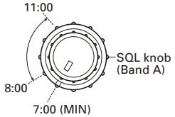 | ||||
| 2) SSG output: -126dBm (0.11μV)SSG MOD: 1kHzSSG DEV: 3kHzAF output: 0.63V/8Ω | Squelch open.BUSY icon appears andS-meter display does notappear. | |||||||
| • 430MHz band | 3) Frequency: 435.250MHz E,M4Frequency: 444.250MHz KSSG output: OFFSet to the point where noise will be muted by turning the SQL knob (Band A). | SQL knob (Band A) position:8:00~11:00BUSY icon disappear.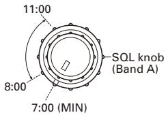 | ||||||
| 4) SSG output: -126dBm (0.11μV)SSG MOD: 1kHzSSG DEV: 3kHzAF output: 0.63V/8Ω | Squelch open.BUSY icon appears andS-meter display does notappear. | |||||||
| Band B• 144MHz band | 5) Frequency: 145.250MHz E,M4Frequency: 146.250MHz KSSG output: OFFSet to the point where noise will be muted by turning the SQL knob (Band B). | SQL knob (Band B) position:8:00~11:00BUSY icon disappear.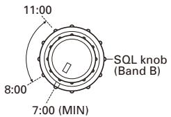 | ||||||
| 6) SSG output: -126dBm (0.11μV)SSG MOD: 1kHzSSG DEV: 3kHzAF output: 0.63V/8Ω | Squelch open.BUSY icon appears andS-meter display does notappear. | |||||||
ADJUSTMENT
| Item | Condition | Measurement | Adjustment | Specifications / Remarks | ||||
| Test-equipment | Unit | Terminal | Unit | Parts | Method | |||
| 430MHz band | 7) Frequency: 435.250MHz E,M4Frequency: 444.250MHz KSSG output: OFFSet to the point where noise will be muted by turning the SQL knob (Band B). | SSG Oscilloscope | TX/RX unit (Rear) | ANTEXT.SP | Check | SQL knob (Band B) position:8:00~11:00BUSY icon disappear.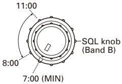 | ||
| 8) SSG output: -126dBm (0.11μV)SSG MOD: 1kHzSSG DEV: 3kHzAF output: 0.63V/8Ω | Squelch open.BUSY icon appears and S-meter display does not appear. | |||||||
| 5. S-meter Check Band A144MHz band S1 | 1) Frequency: 145.250MHz E,M4Frequency: 146.250MHz KSSG MOD: 1kHzSSG DEV: 3kHzSSG output:-118dBm (0.28μV)±3dB | SSG | ANT | Check | One segment in S-meter lights.■■■ | |||
| 144MHz band Full scale | SSG output:-96dBm (3.54μV)±3dB | All segments in S-meter light. | ||||||
| 430MHz band S1 | 2) Frequency: 435.000MHz E,M4Frequency: 444.000MHz KSSG output:-118dBm (0.28μV)±3dB | One segment in S-meter lights.■■■ | ||||||
| 430MHz band Full scale | SSG output:-96dBm (3.54μV)±3dB | All segments in S-meter light. | ||||||
| Band B144MHz band S1 | 3) Frequency: 145.250MHz E,M4Frequency: 146.250MHz KSSG MOD: 1kHzSSG DEV: 3kHzSSG output:-118dBm (0.28μV)±3dB | One segment in S-meter lights.■■■ | ||||||
| 144MHz band Full scale | SSG output:-96dBm (3.54μV)±3dB | All segments in S-meter light. | ||||||
| 430MHz band S1 | 4) Frequency: 435.000MHz E,M4Frequency: 444.000MHz KSSG output:-118dBm (0.28μV)±3dB | One segment in S-meter lights.■■■ | ||||||
| 430MHz band Full scale | SSG output:-96dBm (3.54μV)±3dB | All segments in S-meter light. | ||||||
TM-D710A/D710E PC BOARD
DISPLAY UNIT (X54-3620-00) (A/4, B/4, C/4, D/4)
Component side view (J79-0141-09)
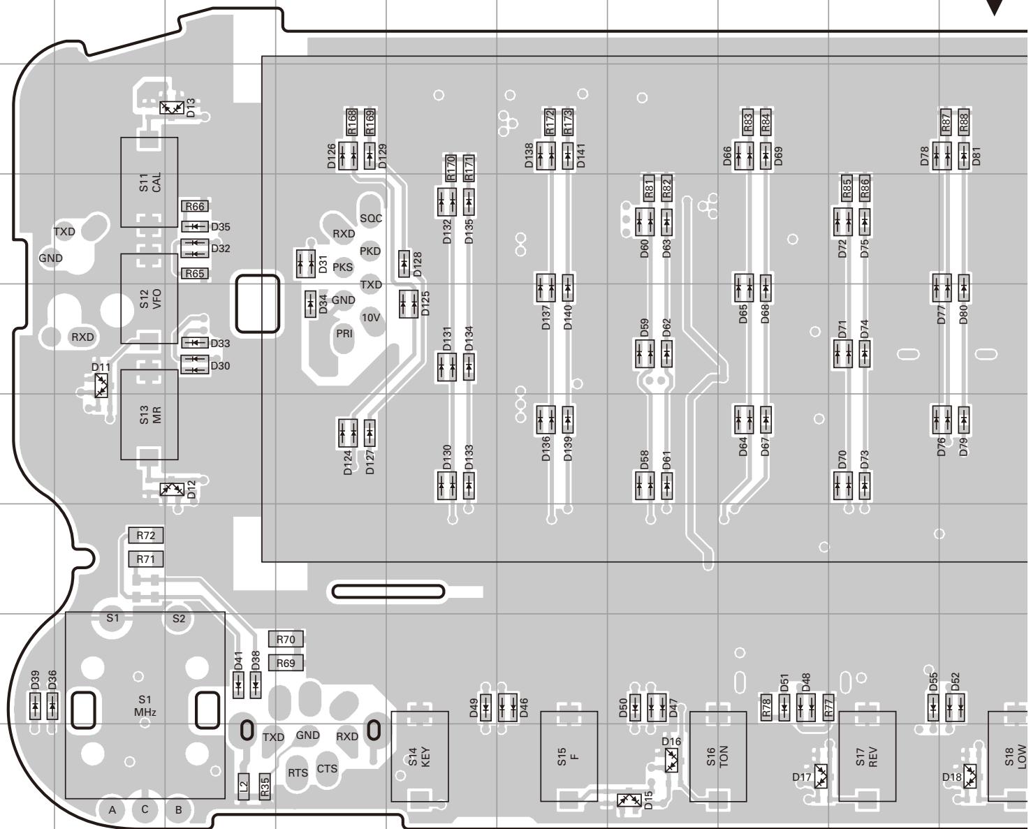
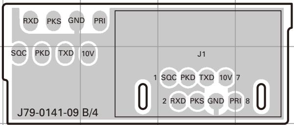
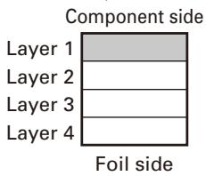
| Ref. No. | Address | Ref. No. | Address | Ref. No. | Address | Ref. No. | Address | Ref. No. | Address |
| D11 | 5B | D28 | 10R | D46 | 8F | D62 | 5G | D78 | 3J |
| D12 | 6C | D29 | 10R | D47 | 8G | D63 | 4G | D79 | 6J |
| D13 | 3C | D30 | 5C | D48 | 8H | D64 | 6H | D80 | 5J |
| D15 | 9G | D31 | 4D | D49 | 8E | D65 | 5H | D81 | 3J |
| D16 | 9G | D32 | 4C | D50 | 8G | D66 | 3H | D82 | 6J |
| D17 | 9H | D33 | 5C | D51 | 8H | D67 | 6H | D83 | 5J |
| D18 | 9J | D34 | 5D | D52 | 8H | D68 | 5H | D84 | 4J |
| D19 | 9K | D35 | 4C | D53 | 8K | D69 | 3H | D85 | 6K |
| D20 | 9L | D36 | 8A | D54 | 8L | D70 | 6I | D86 | 5K |
| D21 | 3Q | D38 | 8C | D55 | 8I | D71 | 5I | D87 | 4K |
| D22 | 5R | D39 | 8A | D56 | 8K | D72 | 4I | D88 | 6K |
| D23 | 4R | D41 | 8C | D57 | 8L | D73 | 6I | D89 | 5K |
| D24 | 13R | D42 | 5Q | D58 | 6G | D74 | 5I | D90 | 3K |
| D25 | 13R | D43 | 4Q | D59 | 5G | D75 | 4I | D91 | 6L |
| D26 | 13R | D44 | 5Q | D60 | 4G | D76 | 6J | D92 | 5L |
| D27 | 10R | D45 | 4Q | D61 | 6G | D77 | 5J | D93 | 3L |
PC BOARD TM-D710A/D710E
DISPLAY UNIT (X54-3620-00) (A/4, B/4, C/4, D/4)
Component side view (J79-0141-09)
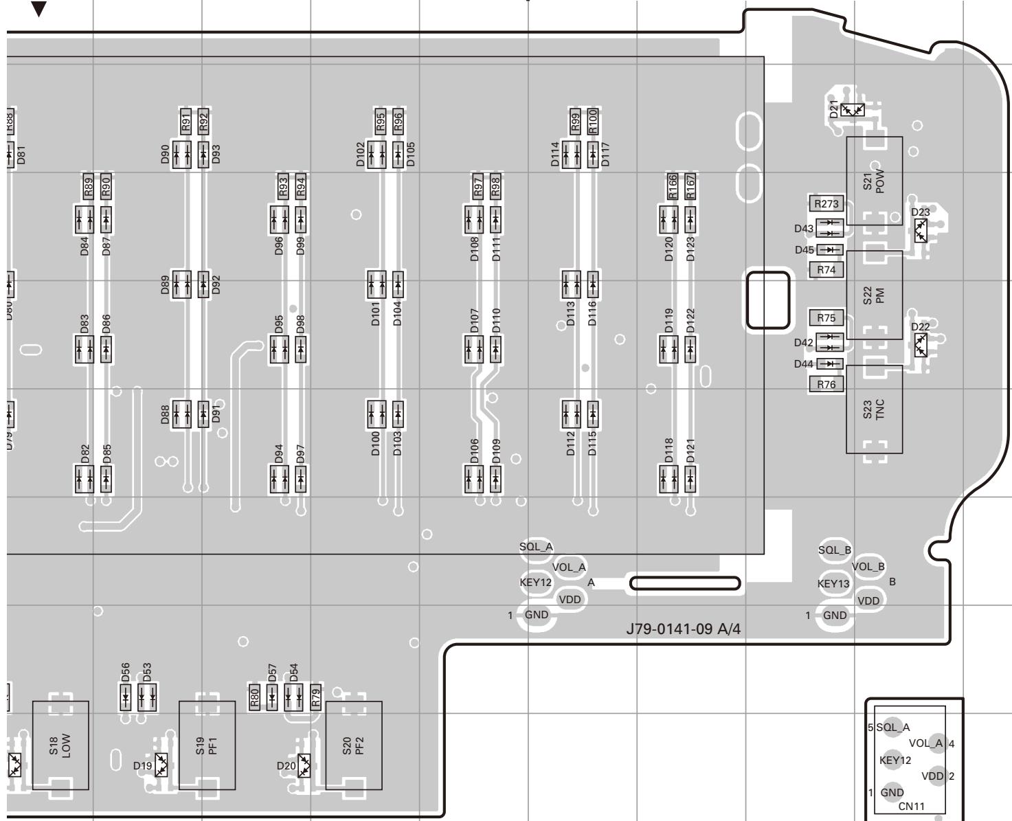

| . | Address | Ref. No. | Address | Ref. No. | Address | Ref. No. | Address |
| 3J | D94 | 6L | D110 | 5N | D126 | 3D | |
| 6J | D95 | 5L | D111 | 4N | D127 | 6D | |
| 5J | D96 | 4L | D112 | 6O | D128 | 4E | |
| 3J | D97 | 6L | D113 | 5O | D129 | 3D | |
| 6J | D98 | 5L | D114 | 3O | D130 | 6E | |
| 5J | D99 | 4L | D115 | 6O | D131 | 5E | |
| 4J | D100 | 6M | D116 | 5O | D132 | 4E | |
| 6K | D101 | 5M | D117 | 3O | D133 | 6E | |
| 5K | D102 | 3M | D118 | 6P | D134 | 5E | |
| 4K | D103 | 6M | D119 | 5P | D135 | 4E | |
| 6K | D104 | 5M | D120 | 4P | D136 | 6F | |
| 5K | D105 | 3M | D121 | 6P | D137 | 5F | |
| 3K | D106 | 6N | D122 | 5P | D138 | 3F | |
| 6L | D107 | 5N | D123 | 4P | D139 | 6F | |
| 5L | D108 | 4N | D124 | 6D | D140 | 5F | |
| 3L | D109 | 6N | D125 | 5E | D141 | 3F |
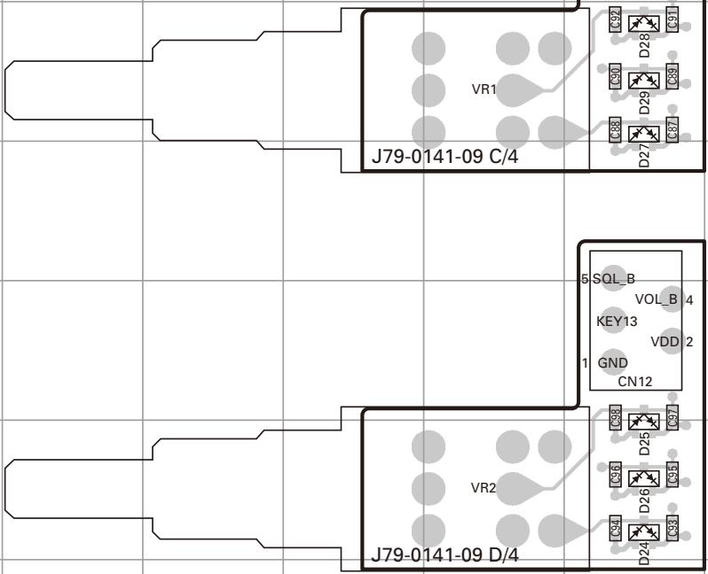
TM-D710A/D710E PC BOARD
DISPLAY UNIT (X54-3620-00) (A/4, B/4, C/4, D/4)
Foil side view (J79-0141-09)
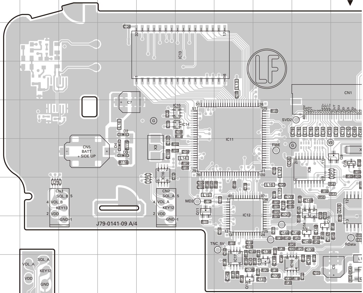
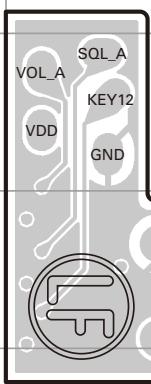
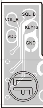
| Ref. No. | Address | Ref. No. | Address | Ref. No. | Address | Ref. No. | Address |
| IC1 | 4M | IC16 | 6E | Q5 | 8L | D4 | 6D |
| IC2 | 6L | IC17 | 9G | Q6 | 9L | D8 | 9Q |
| IC3 | 6L | IC18 | 7I | Q7 | 8L | D9 | 9R |
| IC4 | 3O | IC19 | 6K | Q9 | 6J | D10 | 8R |
| IC5 | 3P | IC20 | 7J | Q10 | 5O | D14 | 9O |
| IC6 | 7N | IC21 | 3P | Q11 | 7F | ||
| IC7 | 9N | IC22 | 3Q | Q12 | 9G | ||
| IC8 | 6I | IC23 | 3R | Q13 | 9H | ||
| IC10 | 9I | IC24 | 5O | Q14 | 8I | ||
| IC11 | 6G | IC25 | 6K | Q15 | 8I | ||
| IC12 | 7G | Q1 | 5N | Q16 | 6J | ||
| IC13 | 3F | Q2 | 8M | D1 | 5O | ||
| IC14 | 5F | Q3 | 9J | D2 | 5D | ||
| IC15 | 5F | Q4 | 9K | D3 | 6D |
PC BOARD TM-D710A/D710E
DISPLAY UNIT (X54-3620-00) (A/4, B/4, C/4, D/4) Foil side view (J79-0141-09)
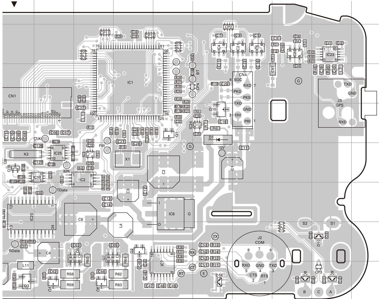

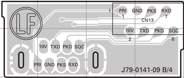
Component side
Foil side
TM-D710A/D710E PC BOARD
TX-RX UNIT
(X57-731X-XX)(A/6):
TX-RX SECTION
PC BOARD TM-D710A/D710E
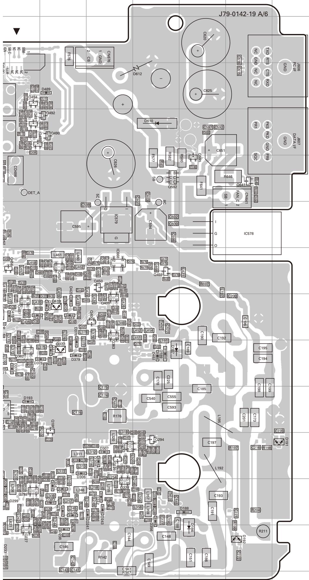
TX-RX UNIT
(X57-731X-XX)(A/6):
TX-RX SECTION
bar_stacked
| Layer | Foil side | |---|---| | Layer 1 | 0 | | Layer 2 | 0 | | Layer 3 | 0 | | Layer 4 | 0 |TM-D710A/D710E PC BOARD
TX-RX UNIT (X57-731X-XX) (D/6) : CONTROL SECTION
0-11 : K 0-21 : M4 2-71 : E Component side view (J79-0142-19 D/6)
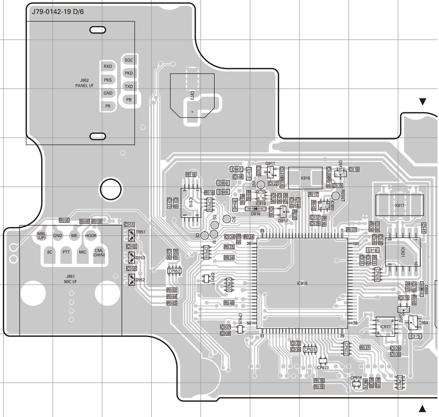
TX-RX UNIT (E/6) : VCO A SECTION
TX-RX UNIT (B/6) : VCO A SECTION
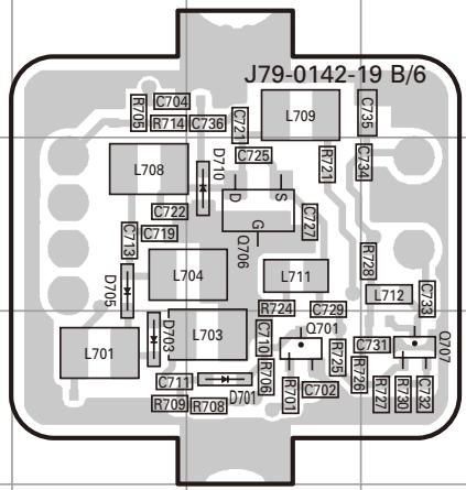
TX-RX UNIT (C/6) :
VCO B SECTION
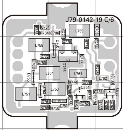
PC BOARD TM-D710A/D710E
TX-RX UNIT (X57-731X-XX) (D/6) : CONTROL SECTION
0-11 : K 0-21 : M4 2-71 : E Component side view (J79-0142-19 D/6)
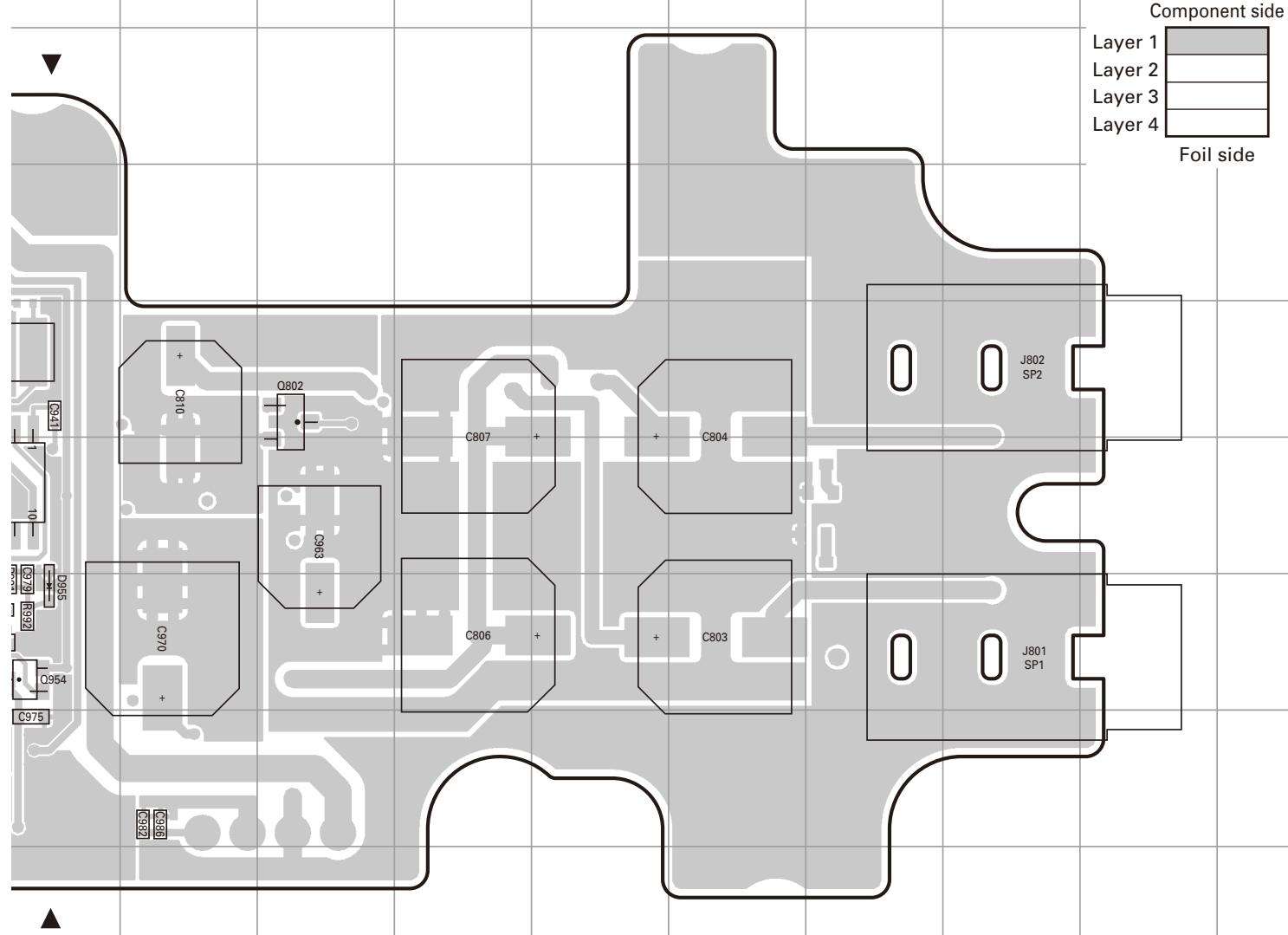
TX-RX UNIT (F/6) :
VCO B SECTION
| Ref. No. | Address | Ref. No. | Address | Ref. No. | Address |
| IC916 | 6E | Q757 | 13J | D751 | 13I |
| IC917 | 8I | Q802 | 6L | D753 | 13H |
| IC918 | 7H | Q916 | 5H | D755 | 12H |
| IC919 | 6G | Q917 | 5G | D760 | 12I |
| IC920 | 6H | Q918 | 6G | D916 | 6G |
| IC921 | 7J | Q952 | 8J | D951 | 6D |
| Q701 | 13F | Q954 | 8J | D952 | 7D |
| Q706 | 12F | D701 | 13F | D953 | 7D |
| Q707 | 13G | D703 | 13E | D955 | 8J |
| Q751 | 13I | D705 | 12E | ||
| Q756 | 12I | D710 | 12F |
TM-D710A/D710E PC BOARD
TX-RX UNIT (X57-731X-XX) (D/6) : CONTROL SECTION
0-11 : K 0-21 : M4 2-71 : E Foil side view (J79-0142-19 D/6)
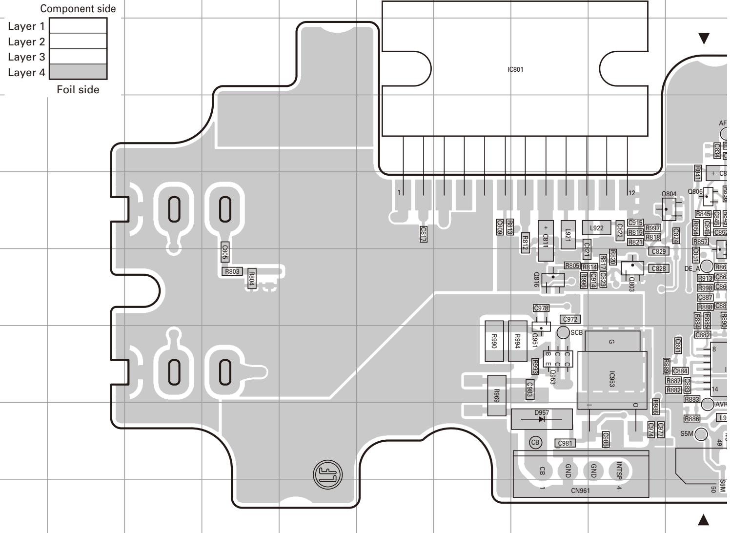
TX-RX UNIT (F/6) : VCO B SECTION
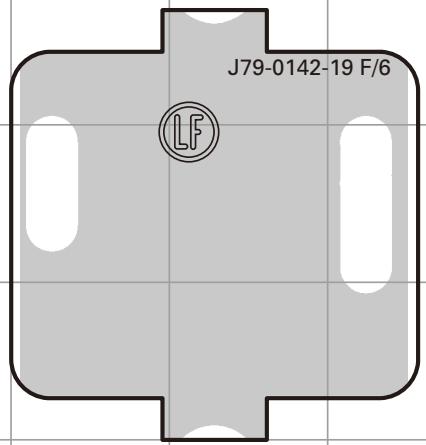
TX-RX UNIT (C/6) : VCO B SECTION
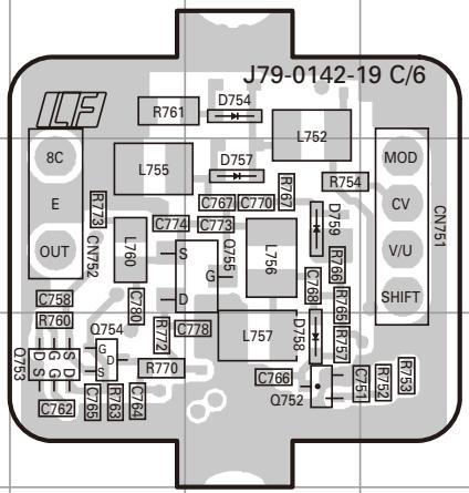
TX-RX UNIT (B/6) : VCO A SECTION
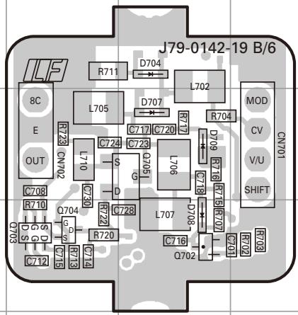
PC BOARD TM-D710A/D710E
TX-RX UNIT (X57-731X-XX) (D/6) : CONTROL SECTION
0-11 : K 0-21 : M4 2-71 : E Foil side view (J79-0142-19 D/6)
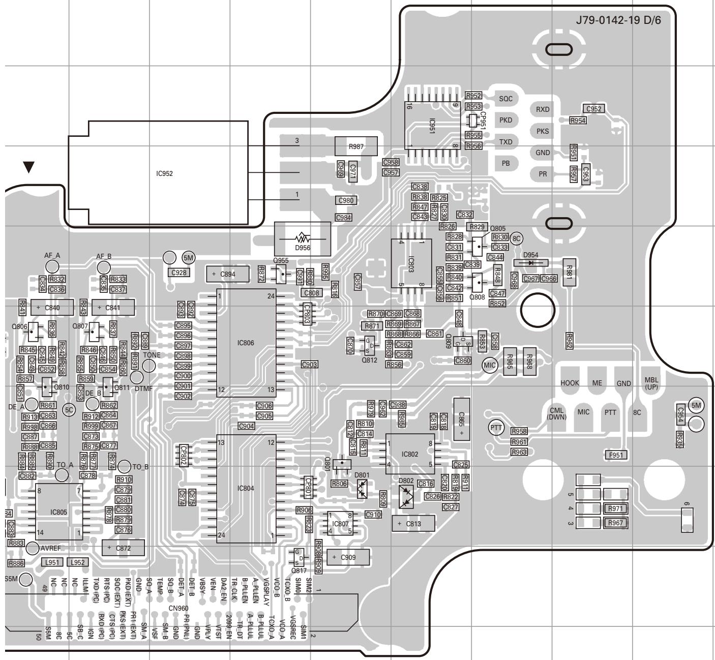
SCHEMATIC DIAGRAM
TM-D710A/D710E
DISPLAY UNIT (X54-3620-00) (A/4)
LCD VDD
LCD_VDD
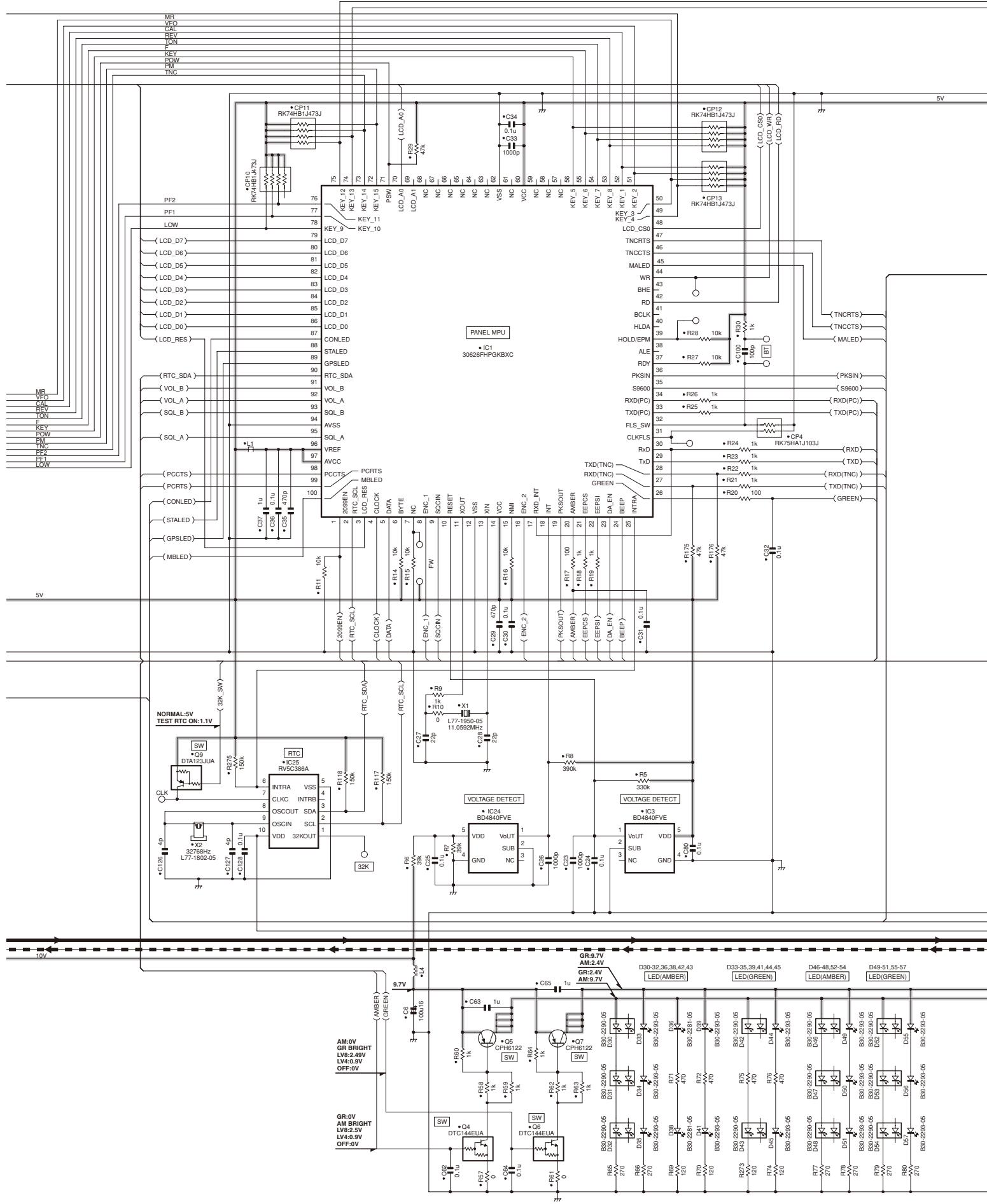
TM-D710A/D710E SCHEMATIC DIAGRAM
DISPLAY UNIT (X54-3620-00) (A/4)
LCD VDD
X54-3620-00 (D/4)
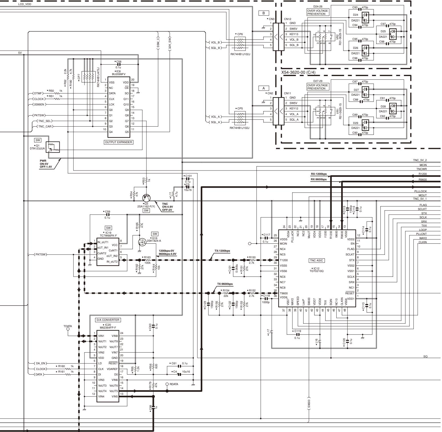
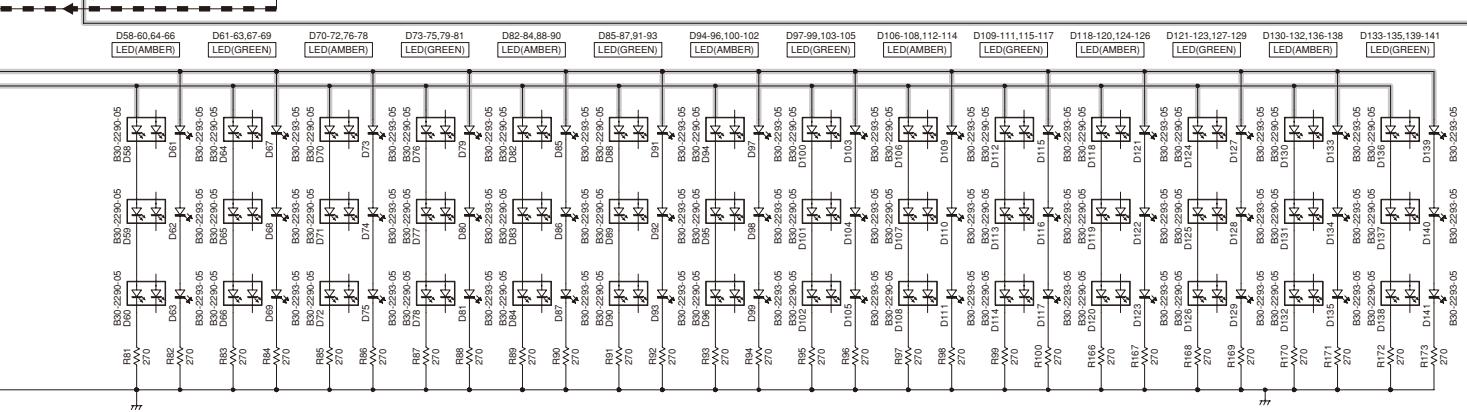
SCHEMATIC DIAGRAM
TM-D710A/D710E
DISPLAY UNIT (X54-3620-00) (A/4)
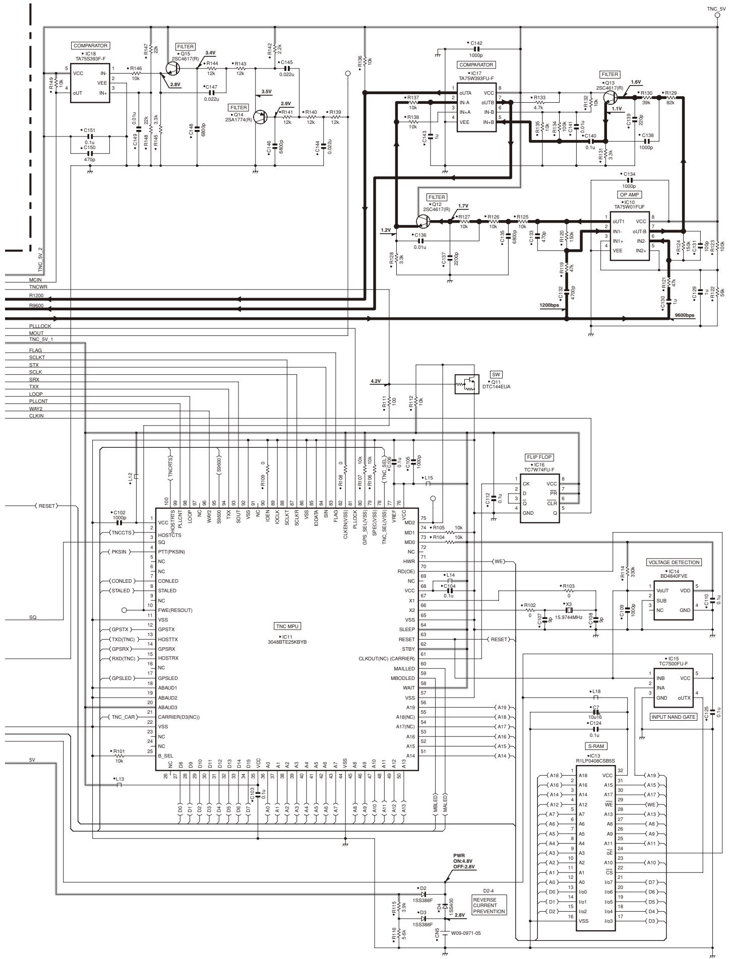
TM-D710A/D710E SCHEMATIC DIAGRAM
TX-RX UNIT (X57-731X-XX)(A/6) : TX-RX SECTION
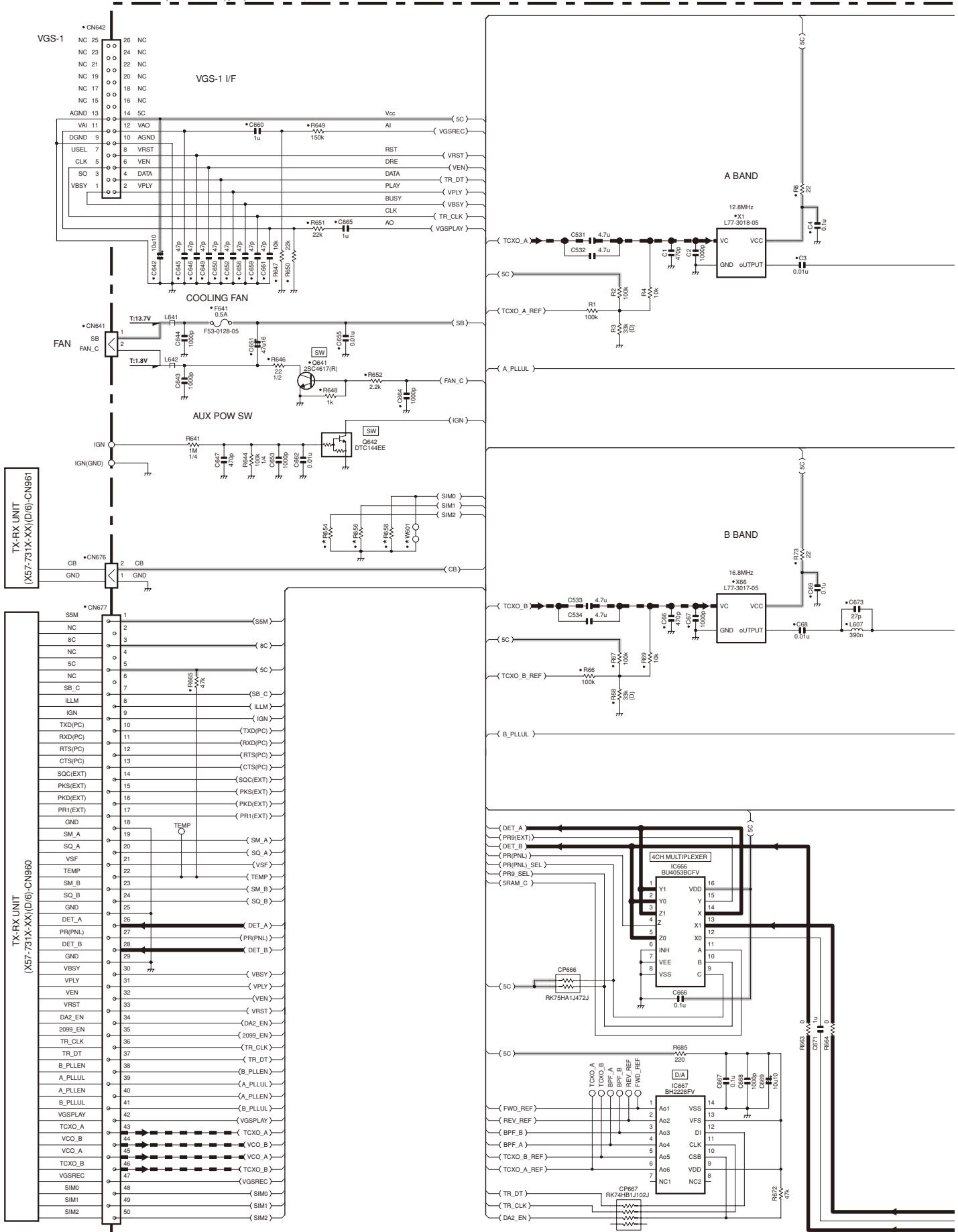
| X57-731X-XX | R654 | R656 | R658 | W601 | |
| 0-11 | K | 0 | 0 | NO | YES |
| 2-71 | E | NO | NO | 0 | NO |
| 0-21 | M4 | NO | 0 | NO | YES |
SCHEMATIC DIAGRAM
TM-D710A/D710E
TX-RX UNIT (X57-731X-XX) (A/6): TX-RX SECTION
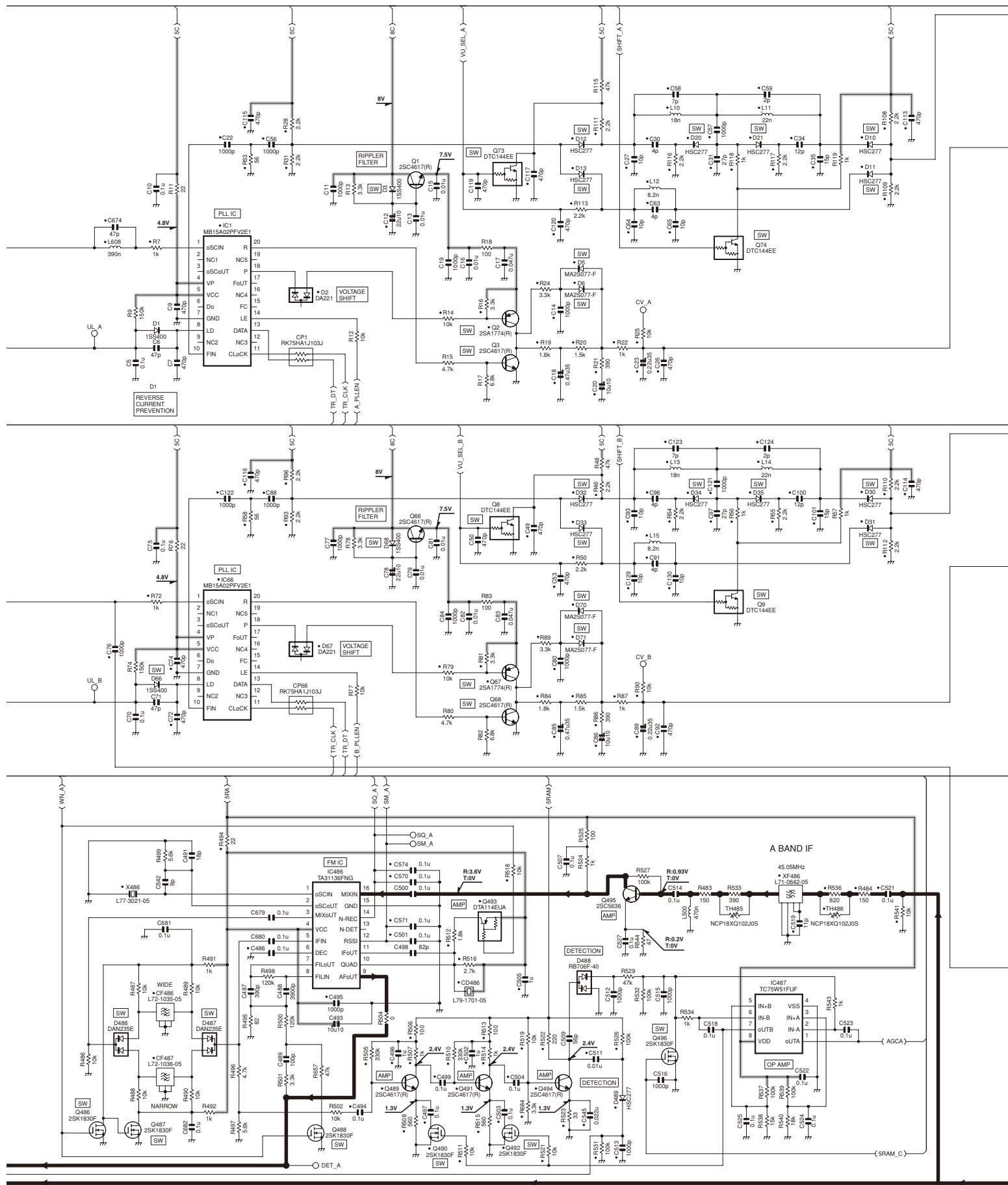
TM-D710A/D710E SCHEMATIC DIAGRAM
TX-RX UNIT (X57-731X-XX) (A/6): TX-RX SECTION
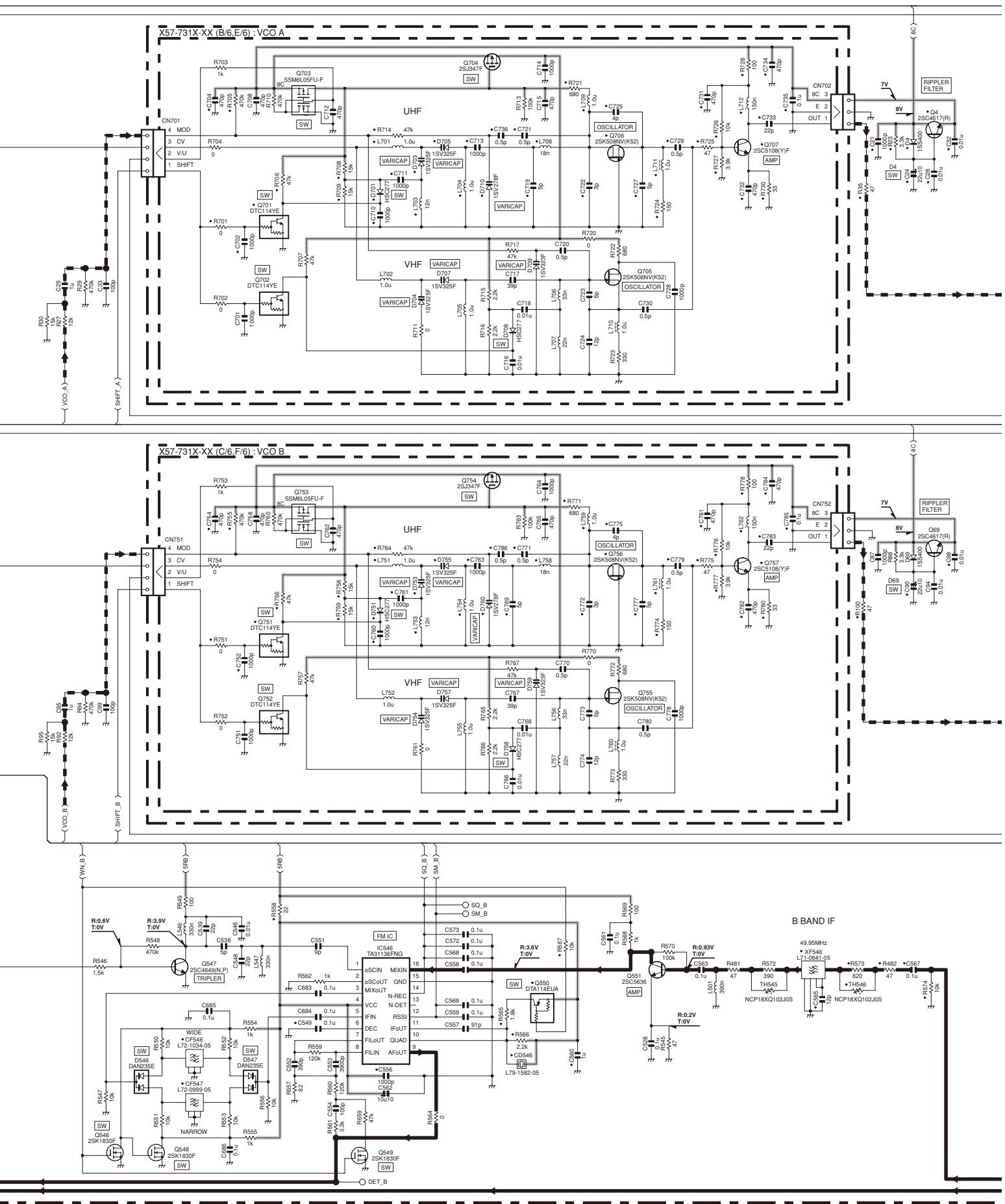
SCHEMATIC DIAGRAM
TM-D710A/D710E
TX-RX UNIT (X57-731X-XX) (A/6): TX-RX SECTION
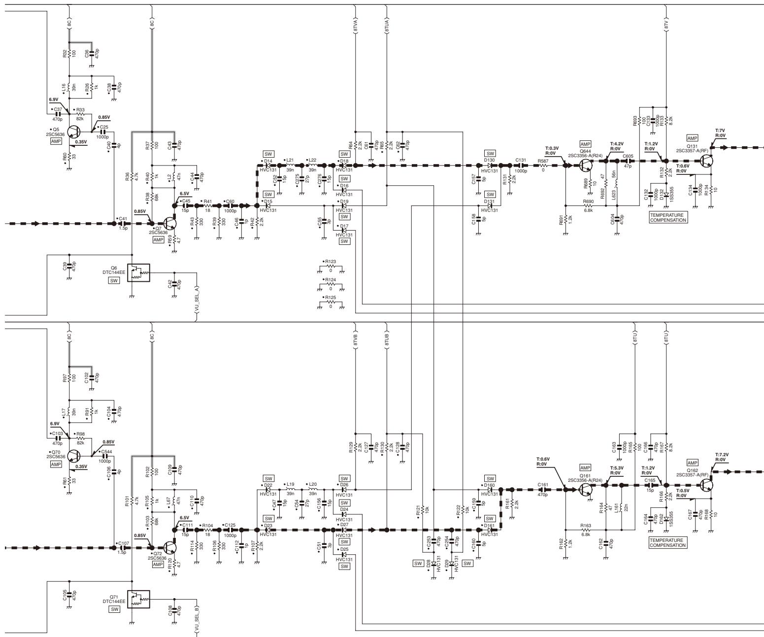
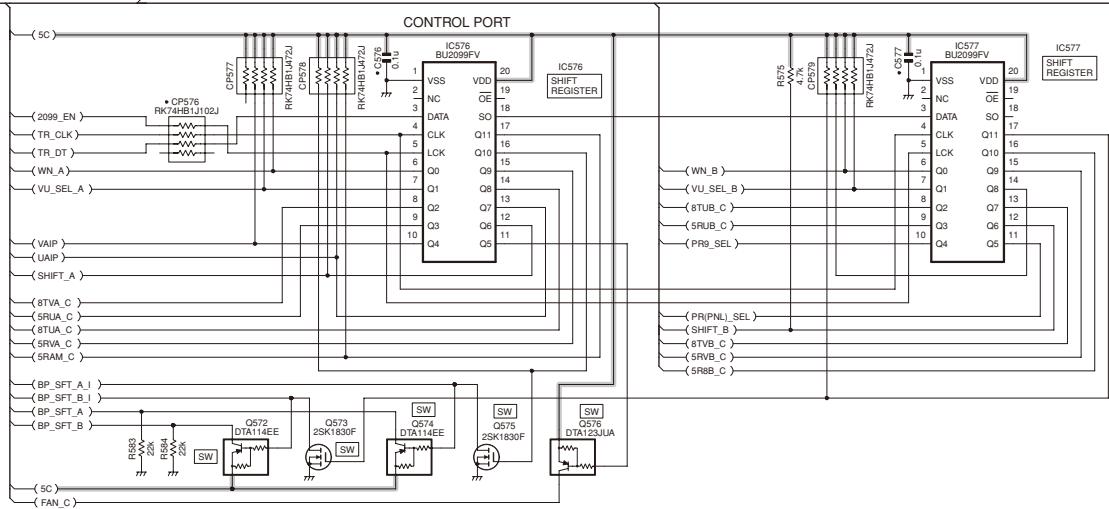
flowchart
graph TD
    subgraph CONTROL_PORT
        A["CP576"] --> B["RK74HB1J102J"]
        C["CP576"] --> D["RK74HB1J47J"]
        E["CP576"] --> F["RK74HB1J47J"]
        G["CP576"] --> H["RK74HB1J47J"]
        I["CP576"] --> J["RK74HB1J47J"]
        K["CP576"] --> L["RK74HB1J47J"]
        M["CP576"] --> N["RK74HB1J47J"]
        O["CP576"] --> P["RK74HB1J47J"]
        Q["CP576"] --> R["RK74HB1J47J"]
        S["CP576"] --> T["RK74HB1J47J"]
        U["CP576"] --> V["RK74HB1J47J"]
        W["CP576"] --> X["RK74HB1J47J"]
        Y["CP576"] --> Z["RK74HB1J47J"]
        AA["CP576"] --> AB["RK74HB1J47J"]
        AC["CP576"] --> AD["RK74HB1J47J"]
        AE["CP576"] --> AF["RK74HB1J47J"]
        AG["CP576"] --> AH["RK74HB1J47J"]
        AI["CP576"] --> AJ["RK74HB1J47J"]
        AK["CP576"] --> AL["RK74HB1J47J"]
        AM["CP576"] --> AN["RK74HB1J47J"]
        AO["CP576"] --> AP["RK74HB1J47J"]
        AQ["CP576"] --> AR["RK74HB1J47J"]
        AS["CP576"] --> AT["RK74HB1J47J"]
        AU["CP576"] --> AV["RK74HB1J47J"]
        AW["CP576"] --> AX["RK74HB1J47J"]
        AY["CP576"] --> AZ["RK74HB1J47J"]
        BA["CP576"] --> BB["RK74HB1J47J"]
        BC["CP576"] --> BD["RK74HB1J47J"]
        BE["CP576"] --> BF["RK74HB1J47J"]
        BG["CP576"] --> BH["RK74HB1J47J"]
        BI["CP576"] --> BJ["RK74HB1J47J"]
        BK["CP576"] --> BL["RK74HB1J47J"]
        BM["CP576"] --> BN["RK74HB1J47J"]
        BO["CP576"] --> BP["RK74HB1J47J"]
        BQ["CP576"] --> BR["RK74HB1J47J"]
        BS["CP576"] --> BT["RK74HB1J47J"]
        BU["CP576"] --> BV["RK74HB1J47J"]
        BW["CP576"] --> BX["RK74HB1J47J"]
        BY["CP576"] --> BZ["RK74HB1J47J"]
        CA["CP576"] --> CB["RK74HB1J47J"]
        CC["CP576"] --> CD["RK74HB1J47J"]
        DE["CP576"] --> DF["RK74HB1J47J"]
        DG["CP576"] --> DH["RK74HB1J47J"]
        DI["CP576"] --> DJ["RK74HB1J47J"]
        DK["CP576"] --> DL["RK74HB1J47J"]
        DM["CP576"] --> DN["RK74HB1J47J"]
        DO["CP576"] --> DA["RK74HB1J47J"]
        DB["CP576"] --> DC["RK74HB1J47J"]
        DD["CP576"] --> DE
        EE["CP576"] --> FD
        FF["CP576"] --> DG
        GG["CP576"] --> DH
        BH["CP576"] --> ID
        IE["CP576"] --> JE
        FL["CP576"] --> GA
        BH["CP576"] --> BH
        BH["CP576"] --> ID
    end

    subgraph CONTROL_PORT
        B
        D
        F
        G
        H
        I
        J
        K
        L
        M
        N
        O
        P
        Q
        R
        S
        T
        U
        V
        W
        X
        Y
        Z
    end

    subgraph CONTROL_PORT
        AA
        AB
        AC
    end

    subgraph CONTROL_PORT
        AA
    end

    subgraph CONTROL_PORT
        AA
    end

    subgraph CONTROL_PORT
        AA
    end

    subgraph CONTROL_PORT
        AA
    end

    subgraph CONTROL_PORT
        AA
    end

    subgraph CONTROL_PORT
        AA
    end

    subgraph CONTROL_PORT
        AA
    end

    subgraph CONTROL_PORT
        AA
    end

    subgraph CONTROL_PORT
        AA
    end
TM-D710A/D710E SCHEMATIC DIAGRAM
TX-RX UNIT (X57-731X-XX) (A/6): TX-RX SECTION
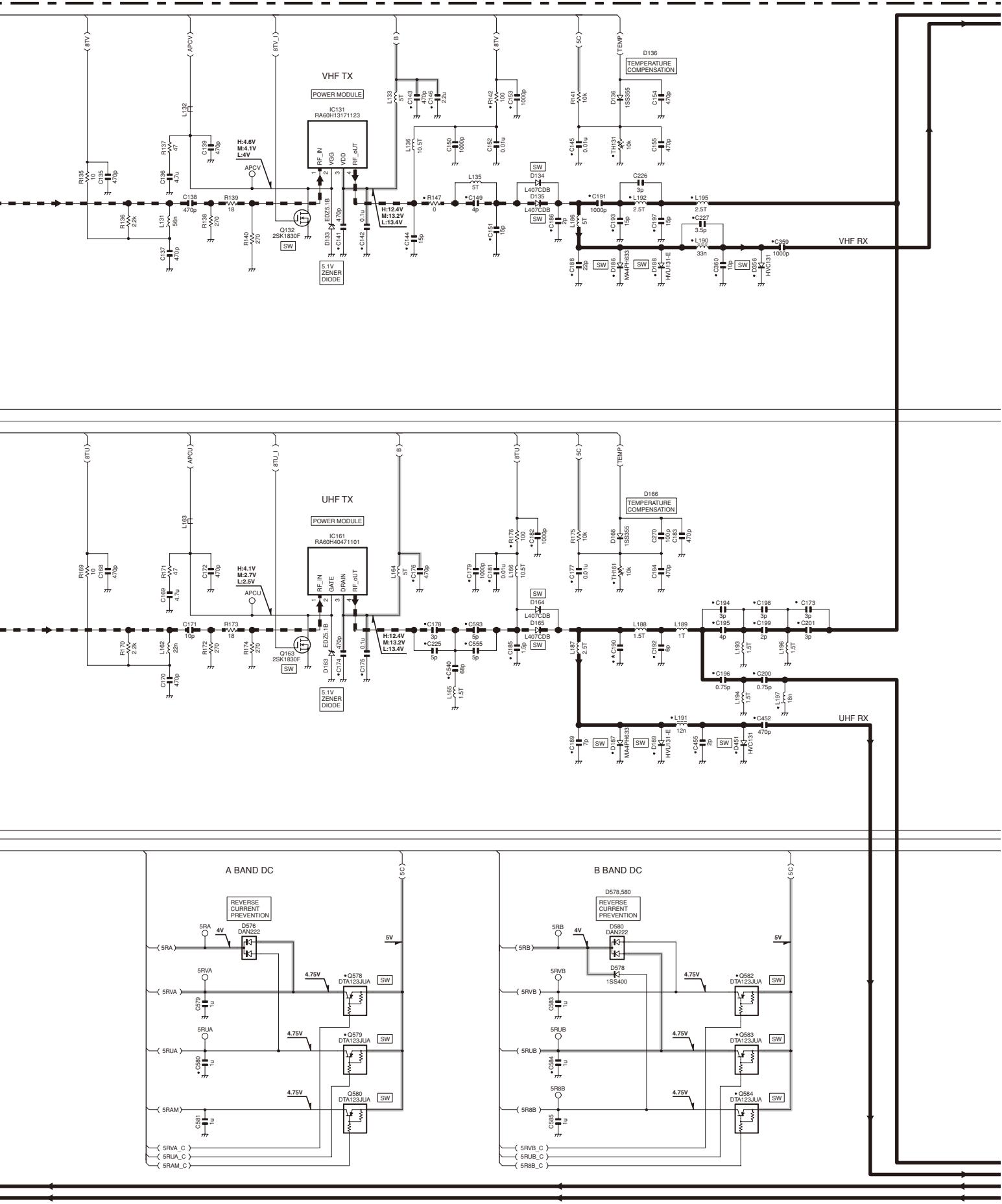
| X57-731X-XX | C190 | |
| 0-11 | K | 4p |
| 2-71 | E | 5p |
| 0-21 | M4 | 4p |
SCHEMATIC DIAGRAM
TM-D710A/D710E
TX-RX UNIT (X57-731X-XX) (A/6): TX-RX SECTION
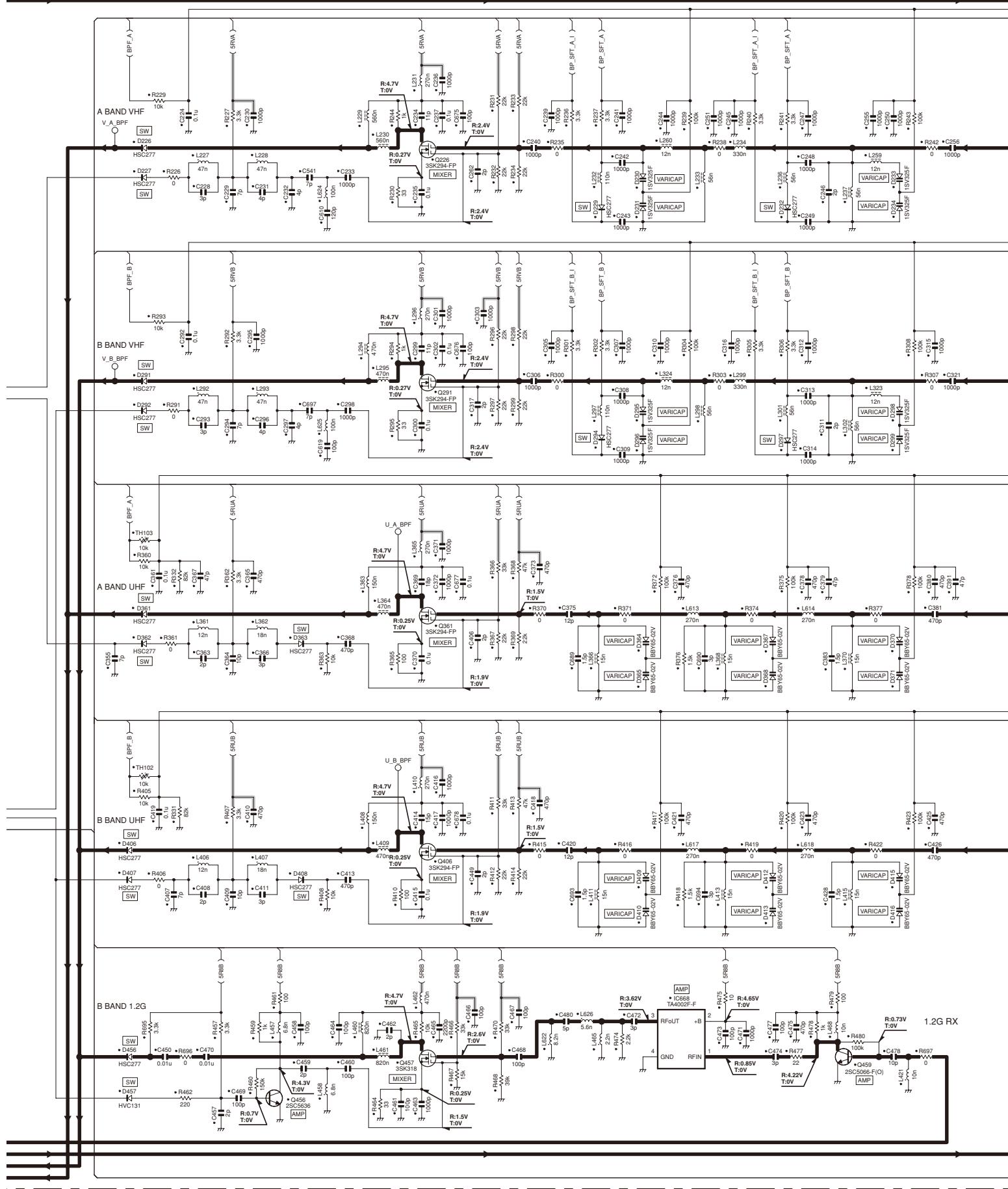
other
The image displays a schematic diagram of an 1.2G RX circuit. It includes multiple top-level (BHF) and bottom-level (BAND) stages. Each stage contains components such as switches, resistors, capacitors, inductors, transistors, and integrated circuits. The circuit is organized in a grid layout with labeled pins (e.g., R229, L227, C451, R303, etc.), each associated with a pin number. The top section includes labels for 'A BAND VHF' and 'B BAND VHF'. The bottom section shows 'A BAND UHF' and 'B BAND UHF'. Key components are interconnected by lines indicating connections between the channels or devices.TM-D710A/D710E SCHEMATIC DIAGRAM
TX-RX UNIT (X57-731X-XX) (A/6): TX-RX SECTION
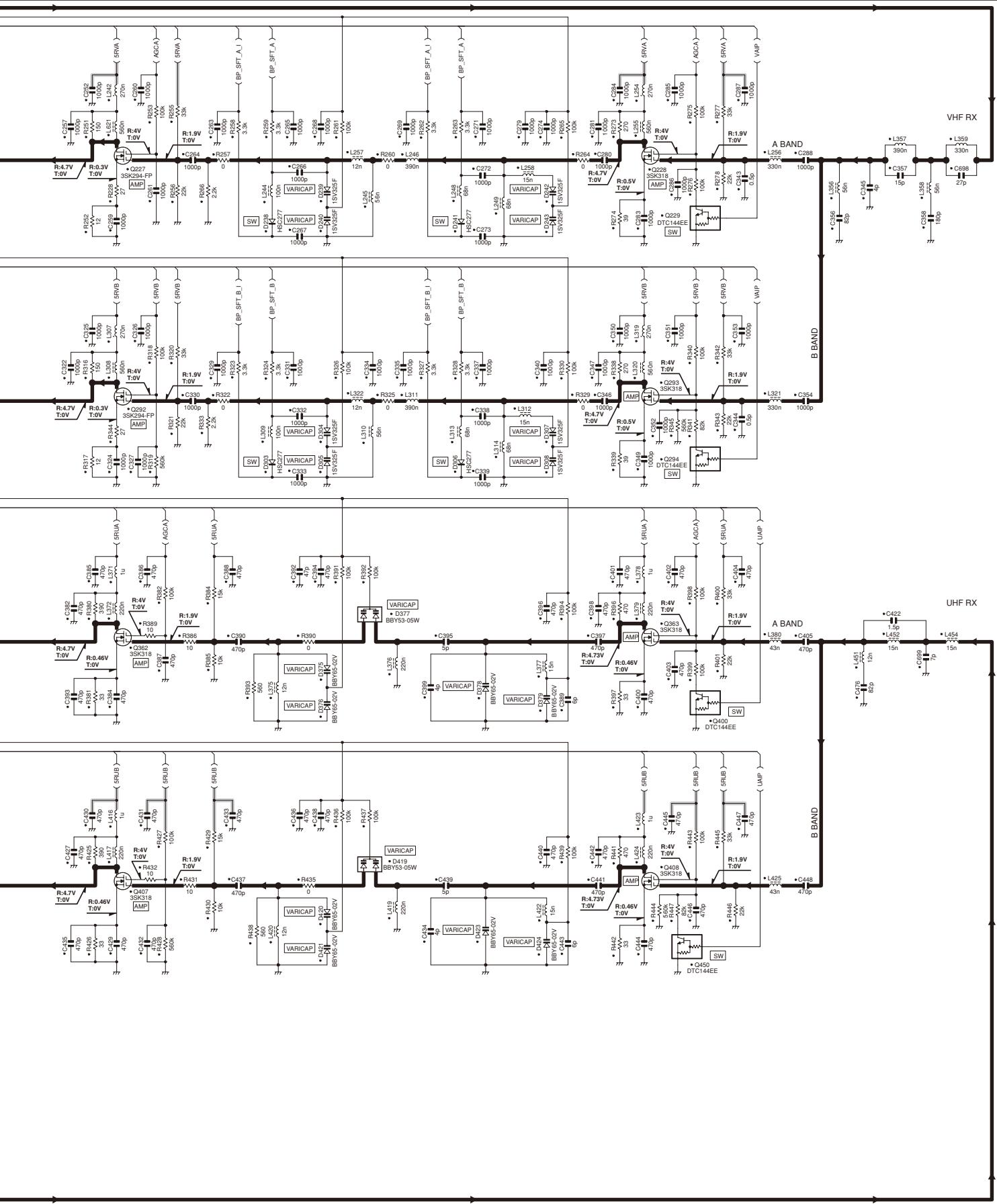
SCHEMATIC DIAGRAM
TM-D710A/D710E
TX-RX UNIT (X57-731X-XX) (A/6): TX-RX SECTION
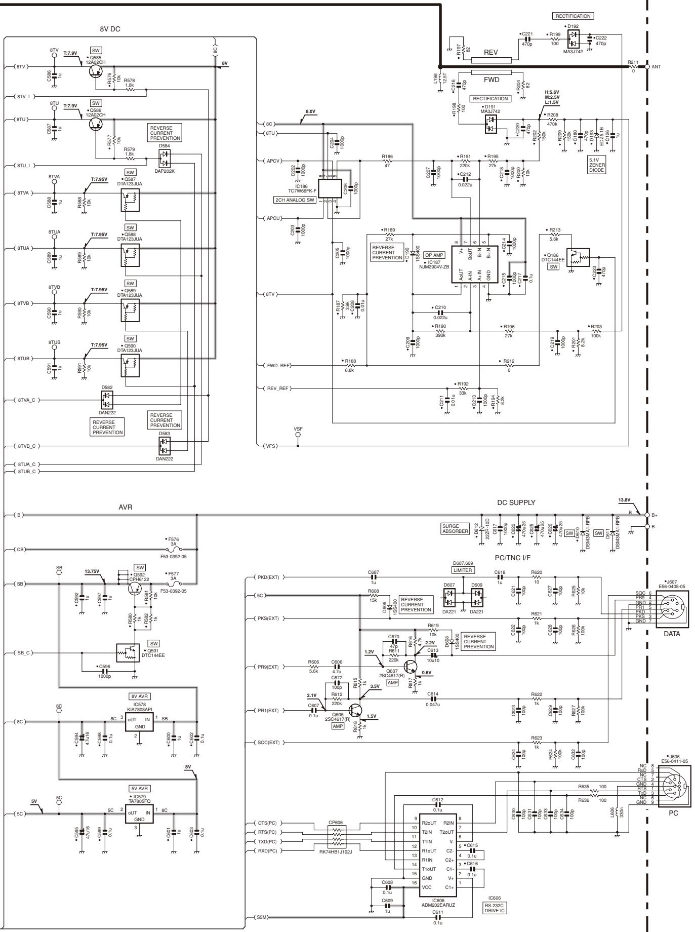
Note : The components marked with a dot (•) are parts of layer 1.
TM-D710A/D710E SCHEMATIC DIAGRAM
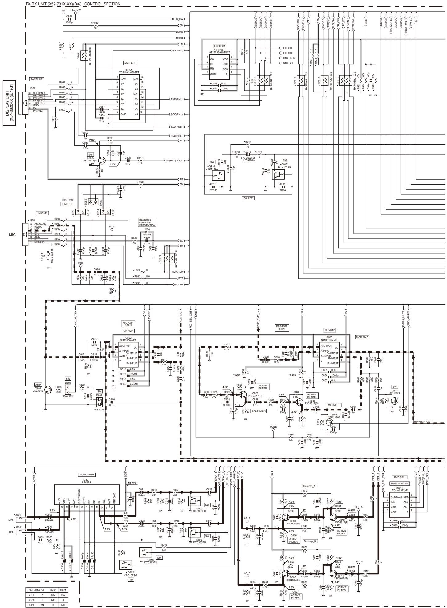
| X57-731X-XX | R967 | R971 | |
| 0-11 | K | NO | NO |
| 2-71 | E | NO | 0 |
| 0-21 | M4 | 0 | NO |
SCHEMATIC DIAGRAM
TM-D710A/D710E
TX-RX UNIT (X57-731X-XX) (D/6): CONTROL SECTION
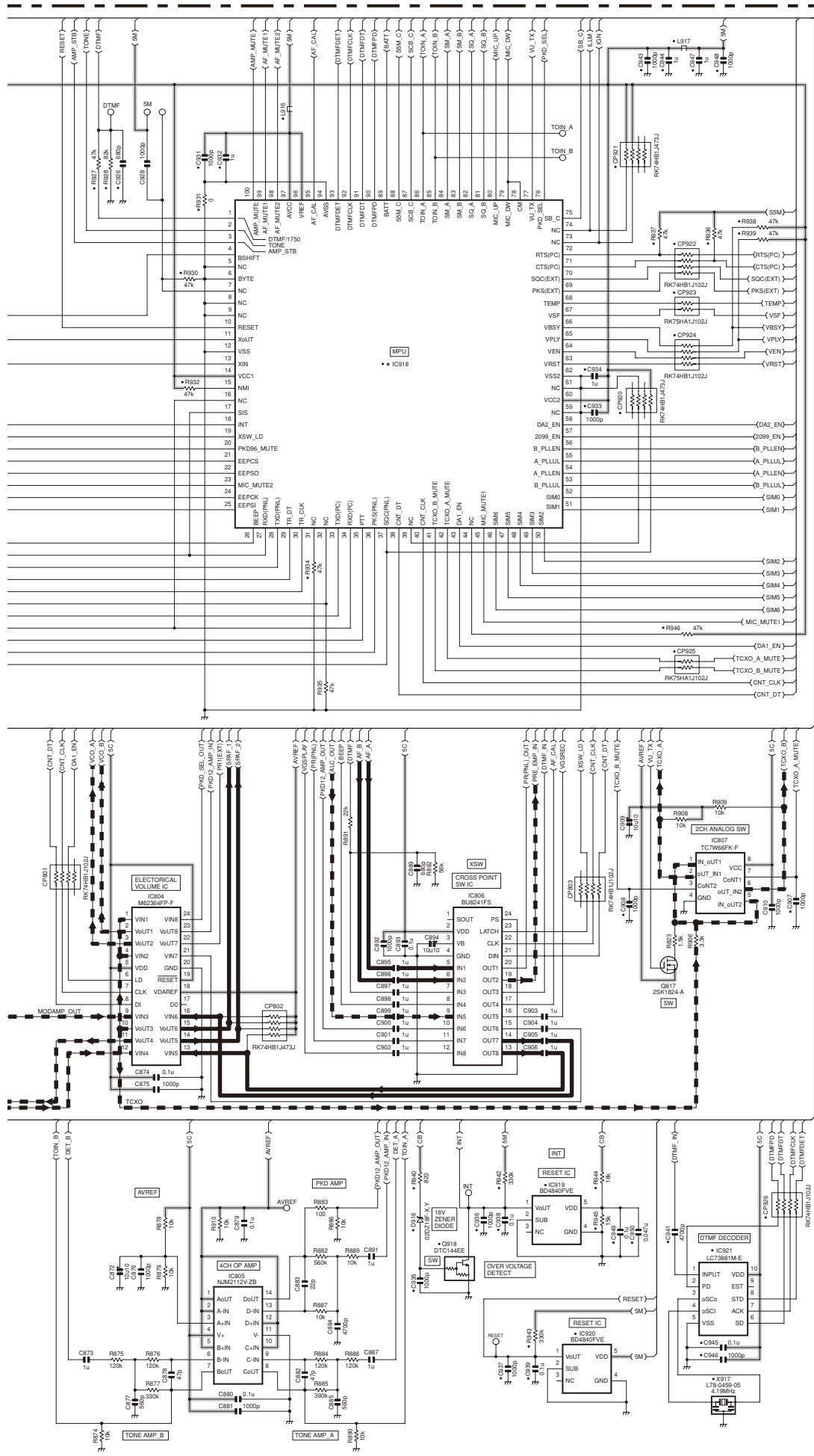
| X57-731X-XX | IC918 | |
| 0-11 | K | 3062LFGPUKBVE |
| 2-71 | E | 3062LFGPUKBWE |
| 0-21 | M4 | 3062LFGPUKBWE |
TM-D710A/D710E BLOCK DIAGRAM
flowchart
graph TD
    A["IC486 TA31136FNG"] --> B["IF DET"]
    B --> C["AGC"]
    C --> D["IF DET"]
    D --> E["IC546 TA31136FNG"]
    E --> F["IF DET"]
    F --> G["IF DET"]
    G --> H["IF DET"]
    H --> I["IF DET"]
    I --> J["IF DET"]
    J --> K["IF DET"]
    K --> L["IF DET"]
    L --> M["IF DET"]
    M --> N["IF DET"]
    N --> O["IF DET"]
    O --> P["IF DET"]
    P --> Q["IF DET"]
    Q --> R["IF DET"]
    R --> S["IF DET"]
    S --> T["IF DET"]
    T --> U["IF DET"]
    U --> V["IF DET"]
    V --> W["IF DET"]
    W --> X["IF DET"]
    X --> Y["IF DET"]
    Y --> Z["IF DET"]
    Z --> A
    subgraph Power Source
        AA["VCO A"] --> AB["Q7 2SC5636"]
        AB --> AC["D14-19 HVC131"]
        AC --> AD["D130,131 HVC131"]
        AD --> AE["RF AMP"]
        AE --> AF["Q644 2SC3356(R24)"]
        AF --> AG["RF AMP"]
        AG --> AH["Q131 2SC3357-A(RF) D132 1SS355"]
        AH --> AI["IC131 VHF POWER MODULE RA60H13171123"]
        AI --> AJ["APCV"]
        AJ --> AK["IC186 NJM2904V-ZB D190: 1SS400"]
        AK --> AL["LPF"]
        AL --> AM["POWER DET D181,192 MA3J742"]
        AM --> AN["+"]
    end

    subgraph Control Source
        AO["VCO B"] --> AP["Q72 2SC5636"]
        AP --> AQ["D22-27 HVC131"]
        AQ --> AR["SW"]
        AR --> AS["D160,161 HVC131"]
        AS --> AT["RF AMP"]
        AT --> AU["Q161 2SC3356(R24)"]
        AU --> AV["RF AMP"]
        AV --> AW["Q162 2SC3357-A(RF) D162 1SS355"]
        AW --> AX["HPF"]
        AX --> AY["IC161 UHF POWER MODULE RA60H40471101"]
        AY --> AZ["APCU"]
        AZ --> BA["IC186 NJM2904V-ZB D190: 1SS400"]
        BA --> BB["LPF"]
        BB --> BC["POWER DET D181,192 MA3J742"]
        BC --> BD["+"]
    end

    subgraph Control Pathway
        BE["Q70: 2SC5636 D30-35: HSC277"] --> BF["SW"]
        BF --> BG["Q8.9 DTC144EE"]
        BF --> BH["MIX"]
        BH --> BI["BPF"]
        BI --> BJ["D229: HSC277 D230,231 1SV225F"]
        BJ --> BK["BPF"]
        BK --> BL["D232: HSC277 D233,234 1SV225F"]
        BL --> BM["BPF"]
        BM --> BN["D238: HSC277 D239,240 1SV225F"]
        BN --> BO["BPF"]
        BO --> BP["D241: HSC277 D242,243 1SV225F"]
        BP --> BQ["BPF"]
        BQ --> BR["D244: HSC277 D245,246 1SV225F"]
        BR --> BS["D247: HSC277 D248,249 1SV225F"]
        BS --> BT["D248: HSC277 D249,250 1SV225F"]
        BT --> BU["BPF"]
        BU --> BV["D249: HSC277 D250,251 1SV225F"]
        BV --> BW["D250: HSC277 D251,252 1SV225F"]
        BW --> BX["BPF"]
        BX --> BY["D250: HSC277 D251,252 1SV225F"]
        BX --> BZ["BPF"]
        BZ --> CA["D250: HSC277 D251,252 1SV225F"]
        CA --> CB["D250: HSC277 D251,252 1SV225F"]
        CB --> CC["D250: HSC277 D251,252 1SV225F"]
        CC --> CD["D250: HSC277 D251,252 1SV225F"]
        CE["X486 TA31136FNG"] --> CF["X486 TA31136FNG"]
        CF["X486 TA31136FNG"] --> CFX["X486 TA31136FNG"]
    end

    subgraph Control Power Supply
        CF["X486 TA31136FNG"] --> CFX["X486 TA31136FNG"]
        CF["X486 TA31136FNG"] --> CFXX["X486 TA31136FNG"]
    end

    subgraph Power Control Pathway
        BZ["X486 TA31136FNG"] --> BZX["X486 TA31136FNG"]
        BZ["X486 TA31136FNG"] --> BZXX["X486 TA31136FNG"]

    subgraph Power Supply
        BZX["X486 TA31136FNG"] --> BZXX["X486 TA31136FNG"]

    subgraph Control Power Supply
        BZX["X486 TA31136FNG"] --> BZXX["X486 TA31136FNG"]

    subgraph Power Supply
        BZX["X486 TA31136FNG"] --> BZXX["X486 TA31136FNG"]

    subgraph Control Power Supply
        BZX["X486 TA31136FNG"] --> BZXI["X486 TA31136FNG"]

    subgraph Power Supply
        BZXI["X486 TA31136FNG"] --> BZXIX["X486 TA31136FNG"]

    subgraph Control Power Supply
        BZXI["X486 TA31136FNG"] --> BZXIX["X486 TA31136FNG"]

    subgraph Power Supply
        BZXI["X486 TA31136FNG"] --> BZXIX["X486 TA31136FNG"]

    subgraph Control Power Supply
        BZXI["X486 TA31136FNG"] --> BZXIX["X486 TA31136FNG"]

    subgraph Control Power Supply
        BZXI["X486 TA31136FNG"] --> BZXIX["X486 TA31136FNG"]

    subgraph Power Supply
        BZXI["X486 TA3113GFG"] --> BZXIX["X486 TA3113GFG"]
    end

    subgraph Control Power Supply
        BZXI["X486 TA3113GFG"] --> BZXIX["X486 TA3113GFG"]

    subgraph Power Supply
        BZXI["X486 TA3113GFG"] --> BZXIX["X486 TA3113GFG"]

    subgraph Control Power Supply
        BZXI["X486 TA3113GFG"] --> BZXIX["X486 TA3113GFG"]

    subgraph Power Supply
        BZXI["X486 TA3113GFG"] --> BZXIX["X486 TA3113GFG"]

    subgraph Control Power Supply
        BZXI["X486 TA3113TFC"] --> BZXIX["X486 TA3113TFC"]

    subgraph Power Supply
        BZXI["X486 TA3113TFC"] --> BZXIX["X486 TA3113TFC"]

    subgraph Control Power Supply
        BZXI["X486 TA3113TFC"] --> BZXIX["X486 TA3113TFC"]

    subgraph Power Supply
        BZXI["X486 TA3113TFC"] --> BZXIX["X486 TA3113TFC"]

    subgraph Control Power Supply
        BZXI["X486 TA311TCFC"] --> BZXIX["X486 TA311TCFC"]

    subgraph Power Supply
        BZXI["X486 TA310FFCG"] --> BZXIX["X486 TA30FFCG"]

    subgraph Control Power Supply
        BZXI["X486 TA30FFCG"] --> BZXIX["X486 TA30FFCG"]

    subgraph Power Supply
        BZXI["X486 TA30FFCG"] --> BZXIX["X486 TA30FFCG"]

    subgraph Control Power Supply
        BZXI["X486 TA30FFCG"] --> BZXIX["X486 TA30FFCG"]

    subgraph Power Supply
        BZXI["X486 TA30FFCG"] --> BZXIX["X486 TA30FFCG"]

    subgraph Control Power Supply
        Bz-XL["TCACTW5W5W5W5W5W5W5W5W5W5W5W5W5W5W5W5W5W5W5W5W5W5W5W5W5W5W5W5W5W5W5W5W5W5W5W5W5W5W5W5W5W5W5W5W5W5W5W5W5W5W<br><br>    end<br><br>    subgraph Control Power Supply<br>        C-XL[TCACTW5W5W5W5W5W5W5W5W5W5W5W5W5W5W5W5W5W5W5W5W5W5W5W5W5W5W5W5W5W<br><br>    end<br><br>    subgraph Control Power Supply<br>        C-XL[TCACTW5W5W5W5W5W5W5W5W5W5W5SWSWSWSWSWSWSWSWSWSWSWSWSWSWSWSWSWSWSWSWSWSWSWSWSWSWSWSWSWSWSWSWSWSWSWSWSWSWSWSWSWSWSWSWSWSWSWSWSWSWSWSWSWSWSWSWSWSWSWSWSWSWSWSWSWSWSWSWSWSWSWSWSWSWSWSWSWSWSWSWSWSWSWSWSWPSPSPSPSPSPSPSPSPSPSPSPSPSPSPSPSPSPSPSPSPSPSPSPSPSPSPSPSPSPSPSPSPSPSPSPSPSPSPSPSPSPSPSPSPSPSPSPSPSPSPSPSPSPSPSPSPSPSPSPSPSPSPSPSPSPSPSPSPSPSPSPSPSPSPSPSPSPSPSPSPSPSPSPSPSPSPSPSPSPSPSPSPSPSPSPSPSPSPSPSPPPRDPRPDPRPDPRPDPRPDPRPDPRPDPRPDPRPDPRPDPRPDPRPDPRPDPRPDPRPDPRPDPRPDPRPDPRPDPRPDPRPDPRPDPRPDPRPDPRPDPRPDPRPDPRPDPRPDPRPDPRPDPRPDPRPDPRPDPRPDPRPDPRPDPRPDPRPDPRPDPRPDPRPDPRPDPRPDPRPDPRPDPRPDPRPDPRPDPRPDPRPDPARPAPRDPAPRDPAPRDPAPRDPAPRDPAPRDPAPRDPAPRDPAPRDPAPRDPAPRDPAPRDPAPRDPAPRDPAPRDPAPRDPAPRDPAPRDPAPRDPAPRDPAPRDPAPRDPAPRDPAPRDPAPRDPAPRDPAPRDPAPRDPAPRDPAPRDPAPRDPAPRDPAPRDPAPRDPARPDPAPRDPAPRDPAPRDPAPRDPAPRDPAPRDPAPRDPAPRDPAPRDPAPRDPAPRDPAPRDPAPRDPAPRDPAPRDPAPRDPAPRDPAPRDPAPRDPAPRDPAPRDPAPRDPAPRDPAPRDPAPRDPAPRDPAPRDPAPRDPAPRDPAPRDPAPRDPAPRDPAPRTPRP RP DP RP DP RP DP RP DP RP DP RP DP RP DP RP DP RP DP RP DP RP DP RP DP RP DP RP DP RP DP RP DP RP DP RP DP RP DP RP DP RP DP RP DP RP DP RP DP RP DP RP DP RP DP RP DP RP DP RP DP RP DP RP DP RP DP RP DP RP DP RP DP RP DP RP DP RP DP RP DP RP DP RP DP RP DP RP DP RP DP RP DP RP DP RP DP RP DP RP DP RP GPPTRP RP GPPTRP GPPTRP GPPTRP GPPTRP GPPTRP GPPTRP GPPTRP GPPTRP GPPTRP GPPTRP GPPTRP GPPTRP GPPTRP GPPTRP GPPTRP GPPTRP GPPTRP GPPTRP GPPTRP GPPTRP GPPTRP GPPTRP GPPTRP GPPTRP GPPTRP GPPTRP GPPTRP GPPTRP GPPTRP GPPTRP GPPTRP GPPTRP GPPTRP GPPTRPGPPTRP GPPTRP GPPTRP GPPTRP GPPTRP GPPTRP GPPTRP GPPTRP GPPTRP GPPTRP GPPTRP GPPTRP GPPTRP GPPTRP GPPTRP GPPTRP GPPTRP GPPTRP GPPTRP GPPTRP GPPTRP GPPTRP GPPTRP GPPTRP GPPTRP GPPTRP GPPTRP GPPTRP GPPTRP GPPTRP GPPTRP GPPTRP GPPTRP GPHTPBP RP TPBP BP TPBP BP TPBP BP TPBP BP TPBP BP TPBP BP TPBP BP TPBP BP TPBP BP TPBP BP TPBP BP TPBP BP TPBP BP TPBP BP TPBP BP TPBP BP TPBP BP TPBP BP TPBP BP TPBP BP TPBP BP TPBP BP TPBP BP TPBP BP TPBP BP TPBP BP TPBP BP TPBP BP TPBP BP TPBP BP TPBP BP TPBP BP TPBP BP TPBP BP TPRP BP TPRP BP TPRP BP TPRP BP TPRP BP TPRP BP TPRP BP TPRP BP TPRP BP TPRP BP TPRP BP TPRP BP TPRP BP TPRP BP TPRP BP TPRP BP TPRP BP TPRP BP TPRP BP TPRP BP TPRP BP TPRP BP TPRP BP TPRP BP TPRP BP TPRNTRTRTRTRTRTRTRTRTRTRTRTRTRTRTRTRTRTRTRTRTRTRTRTRTRTRTRTRTRTRTRTRTRTRTRTRTRTRTRTRTRTRTRTRTRTRTRTRTRTRTRTRTRTRTRTRTRTRTRTRTRTRTRTRTRTRTRTRTRTRTRTRTRTRTRTRTRTRTRTRTRTRTRTRTRTRTRTRTRTRTRTRTRTRTRTRTRTRTRTRRRRRRRRRRRRRRRRRRRRRRRRRRRRRRRRRRRRRRRRRRRRRRRRRRRRRRRRRRRRRRRRRRRRRRRRRRRRRRRRRRRRRRRRRRRRRRRRRRRRRRRRRRRRRRRRRRRRRRRRRRRRRRRRRRRRRRRRRRRRRRRRRRRRRRRRRRRRRRRRRRRRRRRRRRRRRRRRRRRRRRRRRRRRRRRRRRRRRRRRRSRHHHHHHHHHHHHHHHHHHHHHHHHHHHHHHHHHHHHHHHHHHHHHHHHHHHHHHHHHHHHHHHHHHHHHHHHHHHHHHHHHHHHHHHHHHHHHHHHHHHHHHHHHHHHHHHHHHHHHHHHHHHHHHHHHHHHHHHHHHHHHHHHHHHHHHHHHHHHHHHHHHHHHHHHHHHHHHHHHHHHHHHHHHHHHHHHHHHHHHHHHWHWHWHWHWHWHWHWHWHWHWHWHWHWHWHWHWHWHWHWHWHWHWHWHWHWHWHWHWHWHWHWHWHWHWHWHWHWHWHWHWHWHWHWHWHWHWHWHWHWHWHWHWHWHWHWHWHWHWHWHWHWHWHWHWHWHWHWHWHWHWHWHWHWHWHWHWHWHWHWHWHWHWHWHWHWHWHWHWHWHWHWHWHWHWHWHWHWHWHWHWMWHWMWHWMWHWMWHWMWHWMWHWMWHWMWHWMWHWMWHWMWHWMWHWMWHWMWHWMWHWMWHWMWHWMWHWMWHWMWHWMWHWMWHWMWHWMWHWMWHWMWHWMWHWMWHWMWHWMWHWMWHWMWHWMWHWMWHWMWHWMWHWMWHWMWHWMWHWMWHWMWHWMWHWMWHWMWHWMWHWMWHWMWHWMWHWMWHWMWHWWWWWWWWWWWWWWWWWWWWWWWWWWWWWWWWWWWWWWWWWWWWWWWWWWWWWWWWWWWWWWWWWWWWWWWWWWWWWWWWWWWWWWWWWWWWWWWWWWWWWWWWWWWWWWWWWWWWWWWWWWWWWWWWWWWWWWWWWWWWWWWWWWWWWWWWWWWWWWWWWWWWWWWWWWWWWWWWWWWWWWWWWWWWWWWWWWWWWWWWWWWWWWWWWWWWWWWWWWWWWWWWWWWWWWWWWWWWWWWWWWWWWWWWWWWWWWWWWWWWWWWWWWWWWWWWWWWWWWWWWWWWWWWWWWWWWWWWWWWWWWWWWWWWWWWWWWWWWWWWWWWWWWWWWWWWWWWWWWWWWWWWWWWWWWWWWWWWWWWWWWWWWWWWWWWWWWWWWWWWWWWWWWWWWWWWWWWWWWWWWWWWWWWWWWWWWWWWWWWWWWWWWWWWWWWWWWWWWWWWWWWWWWWWWWWWWWWWWWWWWWWWWWWWWWWWWWWWWWWWWWWWWWWWWWWWWWWWWWWWwwwwwwwwwwwwwwwwwwwwwwwwwwwwwwwwwwwwwwwwwwwwwwwwwwwwwwwwwwwwwwwwwwwwwwwwwwwwwwwwwwwwwwwwwwwwwwwwwwwwwwwwwwwwwwwwwwwwwwwwwwwwwwwwwwwwwwwwwwwwwwwwwwwwwwwwwwwwwwwwwwwwwwwwwwwwwwwwwwwwwwwwwwwwwwwwwwwwwwwwwwwwwwwwwwwwwwwwwwwwwwwwwwwwwwwwwwwwwwwwwwwwwwwwwwwwwwwwwwwwwwwwwwwwwwwwwwwwwwwwwwwwwwwwwwwwwwwwwwwwwwwwwwwwwwwwwwwwwwwwwwwwwwwwwwwwwwwwwwwwwwwwwwwwwwwwwwwwwwwwwwwwwwwwwwwwwwwwwwwwwwwwwwwwwwwwwwwwwwwwwwwwwwwwwwwwwwwwwwwwwwwwwwwwwwwwwwwwwwwwwwwwwwwwwwwwwwwwwwwwwwwwwwwwwwwwwwwwwwwwwwwwwwwwwwwwwwwwwwwwwhwwhwhwhwhwhwhwhwhwhwhwhwhwhwhwhwhwhwhwhwhwhwhwhwhwhwhwhwhwhwhwhwhwhwhwhwhwhwhwhwhwhwhwhwhwhwhwhwhwhwhwhwhwhwhwhwhwhwhwhwhwhwhwhwhwhwhwhwhwhwhwhwhwhwhwhwhwhwhwhwhwhwhwhwhwhwhwhwhwhwhwhwhwhwhwhwhwhwhwhwhWhWhWhWhWhWhWhWhWhWhWhWhWhWhWhWhWhWhWhWhWhWhWhWhWhWhWhWhWhWhWhWhWhWhWhWhWhWhWhWhWhWhWhWhWhWhWhWhWhWhWhWhWhWhWhWhWhWhWhWhWhWhWhWhWhWhWhWhWhWhWhWhWhWhWhWhWhWhWhWhWhWhWhWhWhWhWhWhWhWhWhWhWhWhWhWhWhWhWhWhWhitePower supplies<br>    end<br><br>    subgraph Control Power Supply<br>        A[VCO A"] --> A0["VCO A"] & A0["VCO A"] & A0["VCO A"] & A0["VCO A"] & A0["VCO A"] & A0["VCO A"] & A0["VCO A"] & A0["VCO A"] & A0["VCO A"] & A0["VCO A"] & A0["VCO A"] & A0["VCO A"] & A0["VCO A"] & A0["VCO A"] & A0["VCO A"] & APOA["VCO A"] & APOA["VCO A"] & APOA["VCO A"] & APOA["VCO A"] & APOA["VCO A"] & APOA["VCO A"] & APOA["VCO A"] & APOA["VCO A"] & APOA["VCO A"] & APOA["VCO A"] & APOA["VCO A"] & APOA["VCCO A"] & APOA["VCCO A"] & APOA["VCCO A"] & APOA["VCCO A"] & APOA["VCCO A"] & APOA["VCCO A"] & APOA["VCCO A"] & APOA["VCCO A"] & APOA["VCCO A"] & APOA["VCCO A"] & APOA["VCCoA VCCO A"] & APOA["VCCO A"] & APOA["VCCO A"] & APOA["VCCO A"] & APOA["VCCO A"] & APOA["VCCO A"] & APOA["VCCO A"] & APOA["VCCO A"] & APOA["VCCO A"]
LEVEL DIAGRAM
Receiver Section
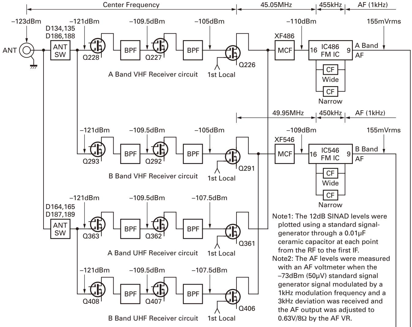
other
| Component | Power Level (dBm) | |-----------|-------------------| | Center Frequency | -121 | | A Band VHF Receiver Circuit | -109.5 | | A Band VHF Receiver Circuit | -105 | | A Band VHF Receiver Circuit | -105 | | A Band VHF Receiver Circuit | -105 | | A Band VHF Receiver Circuit | -105 | | A Band VHF Receiver Circuit | -105 | | A Band VHF Receiver Circuit | -105 | | A Band VHF Receiver Circuit | -105 | | A Band VHF Receiver Circuit | -105 | | A Band VHF Receiver circuit | -121 | | A Band VHF Receiver circuit | -109.5 | | A Band VHF Receiver circuit | -105 | | A Band VHF Receiver circuit | -105 | | A Band VHF Receiver circuit | -105 | | A Band VHF Receiver circuit | -105 | | A Band VHF Receiver circuit | -105 | | A Band VHF Receiver circuit | -105 | | A Band VHF Receiver circuit | -105 | | A Band VHF Receiver circuit | -105 | | A Band VHF Receiver current | -121 | | A Band VHF Receiver current | -109.5 | | A Band VHF Receiver current | -105 | | A Band VHF Receiver current | -105 | | A Band VHF Receiver current | -105 | | A Band VHF Receiver current | -105 | | A Band VHF Receiver current | -105 | | A Band VHF Receiver current | -105 | | A Band VHF Receiver current | -105 | | A Band VHF Receiver current | -105 | | A Band VHF Receiver (First Local) | -121 | | A Band VHF Receiver (First Local) | -109.5 | | A Band VHF Receiver (First Local) | -105 | | A Band VHF Receiver (First Local) | -105 | | A Band VHF Receiver (First Local) | -105 | | A Band VHF Receiver (First Local) | -105 | | A Band VHF Receiver (First Local) | -105 | | A Band VHF Receiver (First Local) | -105 | | A Band VHF Receiver (First Local) | -105 | | Anode Current (AF) | 49.95 MHz | | Anode Current (AF) | 450 kHz | | Anode Current (AF) | 49.95 MHz | | Anode Current (AF) | 450 kHz | | Anode Current (AF) | 49.95 MHz | | Anode Current (AF) | 450 kHz | | Anode Current (AF) | 49.95 MHz | | Anode Current (AF) | 450 kHz | | Anode Current (AF) | -109 dBm | | Anode Current (AF) | -109 dBm | | Anode Current (AF) | -109 dBm | | Anode Current (AF) | -109 dBm | | Anode Current (AF) | -109 dBm | | Anode Current (AF) | -109 dBm | | Anode Current (AF) | -109 dBm | | Anode Current (AF) | 49.95 MHz | | Anode Current (AF) | 450 kHz | | Anode Current (AF) | 49.95 MHz | | Anode Current (AF) | 450 kHz | | Anode Current (AF) | 49.95 MHz | | Anode Current (AF) | 450 kHz | | Anode Current (AF) | Narrow (Narrow) | | Anode Current (AF) | Narrow (Narrow) | | Anode Current (AF) | Narrow (Narrow) | | Anode Current (AF) | Narrow (Narrow) | | Anode Current (AF) | Narrow (Narrow) | | Anode Current (AF) | Narrow (Narrow) | | Anode Current (AF) | Narrow (Narrow) | | Anode Current (AF) | 49.95 MHz | | Anode Current (AF) | 450 kHz | | Anode Current (AF) | 49.95 MHz | | Anode Current (AF) | 450 kHz | | Anode Current (AF) | 49.95 MHz | | Anode Current (AF) | 450 kHz | | Anode Current (AF) | AF (MHz) | | Anode Current (AF) | AF (MHz) | | Anode Current (AF) | AF (MHz) | | Anode Current (AF) | AF (MHz) | | Anode Current (AF) | AF (MHz) | | Anode Current (AF) | AF (MHz) | | Anode Current (AF) | AF (MHz) | | Anode Current (AF) | AF (MHz) | | Anode Current (AF) / AF Voltage Source | 49.95 MHz | | Anode Current (AF Voltage Source) / AF Voltage Source | 450 kHz | | Anode Current (AF Voltage Source) / AF Voltage Source / AF Voltage Source / AF Voltage Source / AF Voltage Source / AF Voltage Source / AF Voltage Source / AF Voltage Source / AF Voltage Source / AF Voltage Source / AF Voltage Source / AF Voltage Source / AF Voltage Source / AF Voltage Source / AF Voltage Source / AF Voltage Source / AF Voltage Source / AF Voltage Source / AF Voltage Source / AF Voltage Source / AF Voltage Source / AF Voltage Source / AF Voltage Source / AF Voltage Source / AF Voltage Source / AF Voltage Source / AF Voltage Sources / AF Voltage Sources / AF Voltage Sources / AF Voltage Sources / AF Voltage Sources / AF Voltage Sources / AF Voltage Sources / AF Voltage Sources / AF Voltage Sources / AF Voltage Sources / AF Voltage Sources / AF Voltage Sources / AF Voltage Sources / AF Voltage Sources / AF Voltage Sources / AF Voltage Sources / AF Voltage Sources / AF Voltage Sources / AF Voltage Sources / AF Voltage Sources / AF Voltage Sources / AF Voltage Sources / AF Voltage Sources / AF Voltage Sources / AF Voltage Sources / AF Voltage Source / AF Voltage Source / AF Voltage Source / AF Voltage Source / AF Voltage Source / AF Voltage Source / AF Voltage Source / AF Voltage Source / AF Voltage Source / AF Voltage Source / AF Voltage Source / AF Voltage Source / AF Voltage Source / AF Voltage Source / AF Voltage Source / AF Voltage Source / AF Voltage Source / AF Voltage Source / AF Voltage Source / AF Voltage Source / AF Voltage Source / AF Voltage Source / AF Voltage Source / AF Voltage Source / AF Voltage Output / Adjusted to 0.63V/8Ω by the AF VR.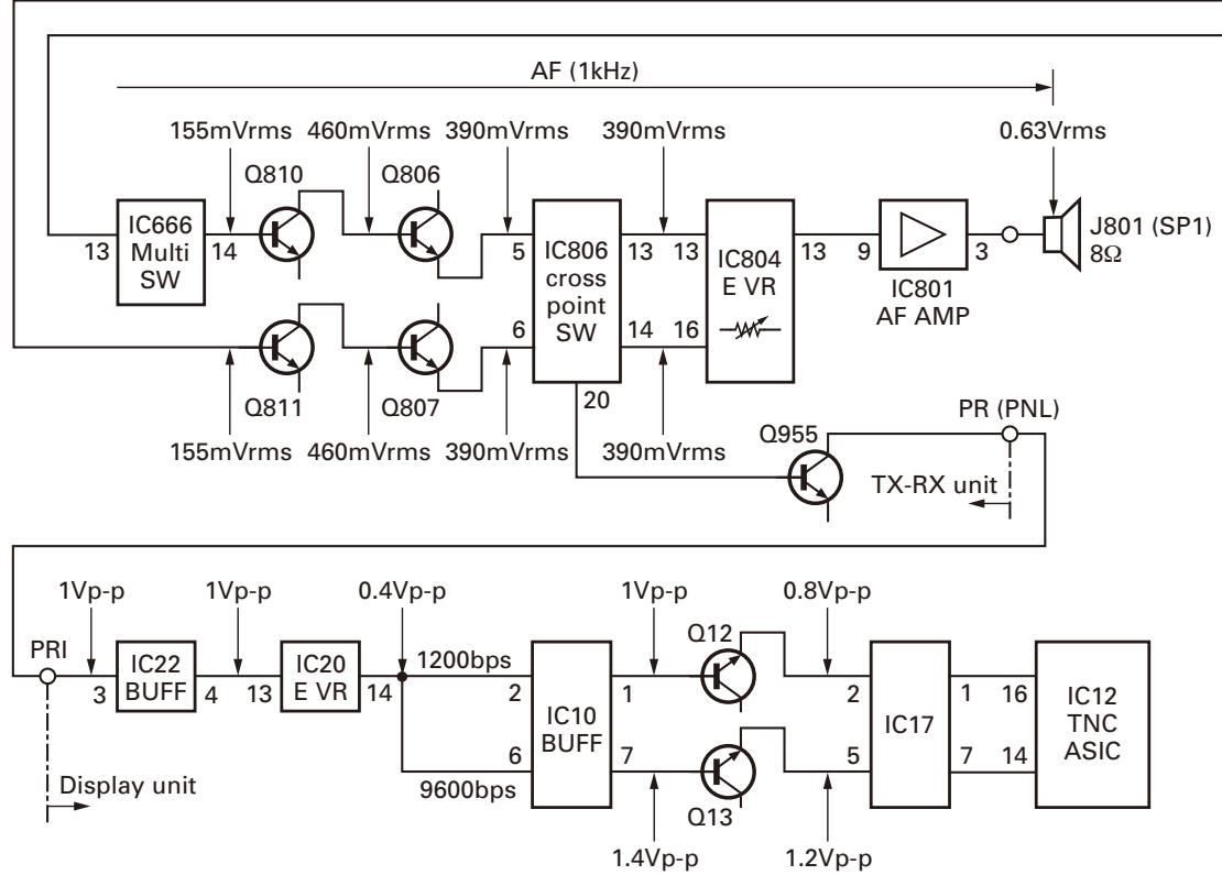
flowchart
graph TD
    A["AC Input"] --> B["IC666 Multi SW"]
    B --> C["IC806 cross point SW"]
    C --> D["IC804 E VR"]
    D --> E["IC801 AF AMP"]
    E --> F["J801 (SP1) 8Ω"]
    G["Display Unit"] --> H["IC22 BUFF"]
    H --> I["IC20 E VR"]
    I --> J["IC10 BUFF"]
    J --> K["IC17"]
    K --> L["IC12 TNC ASIC"]
    M["PR (PNL)"] --> N["TX-RX unit"]
    O["0.63Vrms"] --> P["J801 (SP1)"]
    Q["155mVrms"] --> R["Q810"]
    R --> S["Q806"]
    S --> T["Q811"]
    T --> U["Q807"]
    U --> V["Q806"]
    V --> W["IC806 cross point SW"]
    X["155mVrms"] --> Y["Q811"]
    Y --> Z["Q807"]
    Z --> AA["Q806"]
    AB["1200bps"] --> AC["IC10 BUFF"]
    AD["9600bps"] --> AE["IC10 BUFF"]
    AF["1.4Vp-p"] --> AG["IC17"]
    AH["1.2Vp-p"] --> AI["IC12 TNC ASIC"]
LEVEL DIAGRAM
Transmitter Section
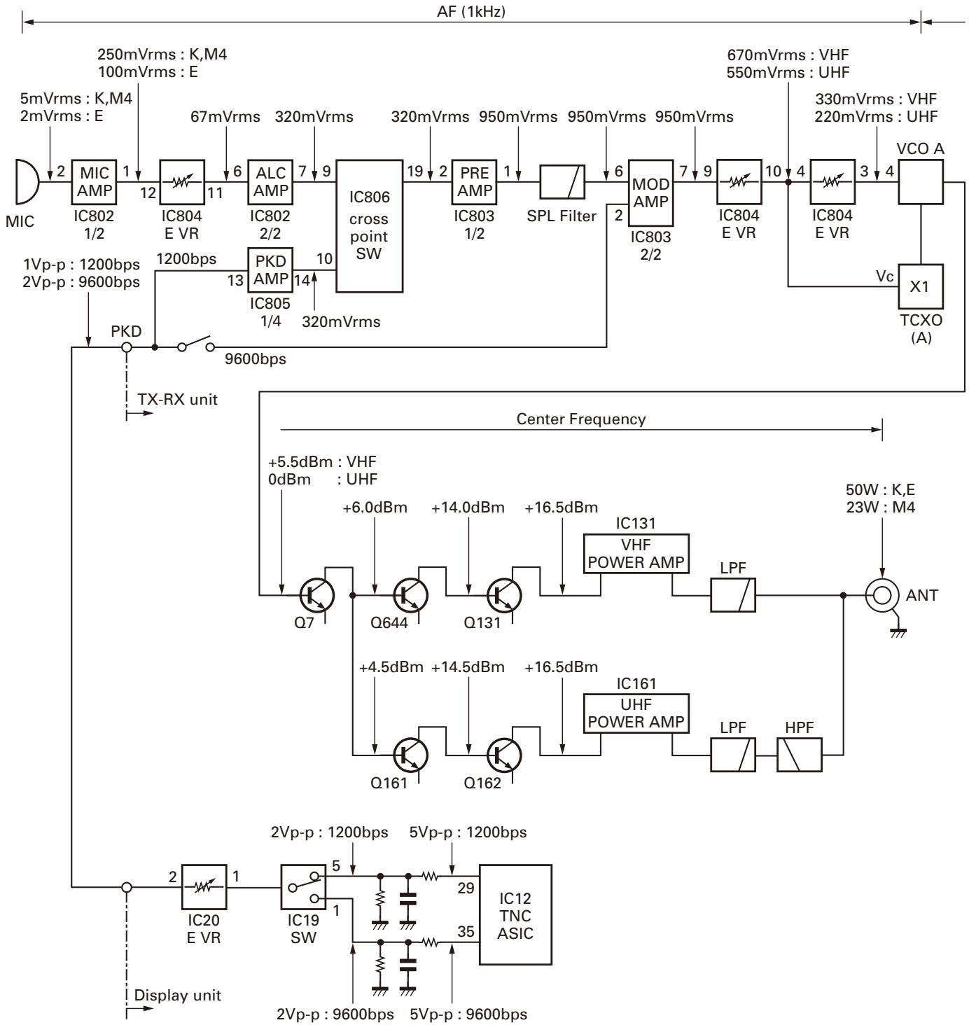
flowchart
graph TD
    A["AF (1kHz)"] --> B["250mVrms: K,M4 100mVrms: E"]
    B --> C["MIC AMP IC802 1/2"]
    C --> D["IC804 E VR"]
    D --> E["67mVrms 320mVrms"]
    E --> F["ALC AMP IC802 2/2"]
    F --> G["IC806 cross point SW"]
    G --> H["PRE AMP IC803 1/2"]
    H --> I["SPL Filter"]
    I --> J["MOD AMP IC803 2/2"]
    J --> K["IC804 E VR"]
    K --> L["VCO A"]
    L --> M["X1 TCXO (A)"]
    M --> N["Vc"]
    N --> O["+5.5dBm VHF 0dBm UHF"]
    O --> P["+6.0dBm +14.0dBm +16.5dBm"]
    P --> Q["IC131 VHF POWER AMP"]
    Q --> R["LPF"]
    R --> S["ANT"]
    S --> T["HPF"]
    T --> U["HPF"]
    U --> V["LPF"]
    V --> W["HPF"]
    W --> X["HPF"]
    X --> Y["LPF"]
    Y --> Z["HPF"]
    Z --> AA["HPF"]
    AA --> AB["LPF"]
    AB --> AC["HPF"]
    AC --> AD["HPF"]
    AD --> AE["LPF"]
    AE --> AF["HPF"]
    AF --> AG["HPF"]
    AG --> AH["LPF"]
    AH --> AI["HPF"]
    AI --> AJ["HPF"]
    AJ --> AK["LPF"]
    AK --> AL["HPF"]
    AL --> AM["HPF"]
    AM --> AN["LPF"]
    AN --> AO["HPF"]
    AO --> AP["HPF"]
    AP --> AQ["LPF"]
    AQ --> AR["HPF"]
    AR --> AS["HPF"]
    AS --> AT["LPF"]
    AT --> AU["HPF"]
    AU --> AV["HPF"]
    AV --> AW["LPF"]
    AW --> AX["HPF"]
    AX --> AY["HPF"]
    AY --> AZ["LPF"]
    AZ --> BA["HPF"]
    BA --> BB["HPF"]
    BB --> BC["LPF"]
    BC --> BD["HPF"]
    BD --> BE["HPF"]
    BE --> BF["LPF"]
    BF --> BG["HPF"]
    BG --> BH["HPF"]
    BH --> BI["LPF"]
    BI --> BJ["HPF"]
    BJ --> BK["HPF"]
    BK --> BL["LPF"]
    BL --> BM["HPF"]
    BM --> BN["HPF"]
    BN --> BO["LPF"]
    BO --> BP["HPF"]
    BP --> BQ["HPF"]
    BQ --> BR["LPF"]
    BR --> BS["HPF"]
    BS --> BT["HPF"]
    BT --> BU["LPF"]
    BU --> BV["HPF"]
    BV --> BW["HPF"]
    BW --> BX["LPF"]
    BX --> BY["HPF"]
    BY --> BZ["HPF"]
Note 1: Set the AG so that the microphone socket input is 3kHz deviation at 1kHz modulation.
The data communication connector input level is 3kHz deviation at 1kHz modulation for 1200bps and 2kHz deviation at 1kHz modulation for 9600bps.
Note 2: Set the transmit power to HI (K,E types) / MID (M4 type).
Note 3: The measurements with the power meter, except for the ANT connector, are the values with the APC off.
Note 4: When measuring the data level as 1200 or 9600 bps, perform the following settings in menu mode:
- BEACON TYPE: APRS (Menu mode: 600)
- DATA SPEED: 1200 bps or 9600 bps (Menu mode: 601)
TM-D710A/D710E
OPTIONAL ACCESSORIES
MC-59 (Keypad Microphone)
■ External View
natural_image
Black Kenwood remote control device with coiled cord and connector (no visible text or symbols)■ Cord Assembly
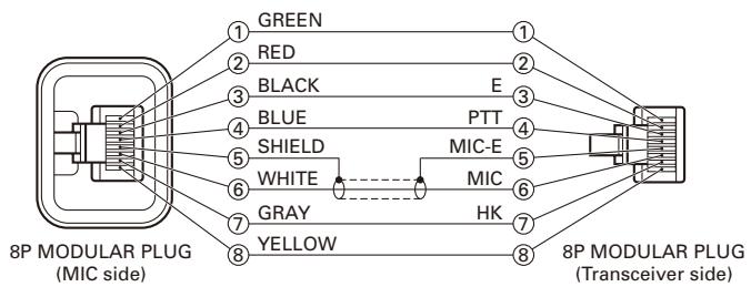
flowchart
graph LR
    A["8P MODULAR PLUG (MIC side)"] -->|1 GREEN| B["8P MODULAR PLUG (Transceiver side)"]
    A -->|2 RED| B
    A -->|3 BLACK| B
    A -->|4 BLUE| B
    A -->|5 SHIELD| B
    A -->|6 WHITE| B
    A -->|7 GRAY| B
    A -->|8 YELLOW| B
    B -->|1 E| C["8P MODULAR PLUG (Transceiver side)"]
    B -->|2 PTT| C
    B -->|3 MIC-E| C
    B -->|4 MIC| C
    B -->|5 HK| C
    B -->|6 HK| C
■ Specifications
Voltage Required 8V±10%
Operating Temperature Range
-20^ +60^ (-4^ +140^)
Current Drain ....Less than 12mA
* Refer to the MC-59 service manual (B51-8804-00) for servicing information, such as circuit diagram, parts list and etc.
PG-5G (Programming Interface Cable (2 m))
■ External View
natural_image
Black cable with connector and connector pin, labeled with number ① (no text or symbols on the cable itself)PARTS LIST
| Ref. No. | New parts | Parts No. | Q'ty | Description |
| 1 | * | E30-7607-05 | 1 | PC cable (2m) |
PG-5F (Extension Cable Kit (4 m))
■ External View
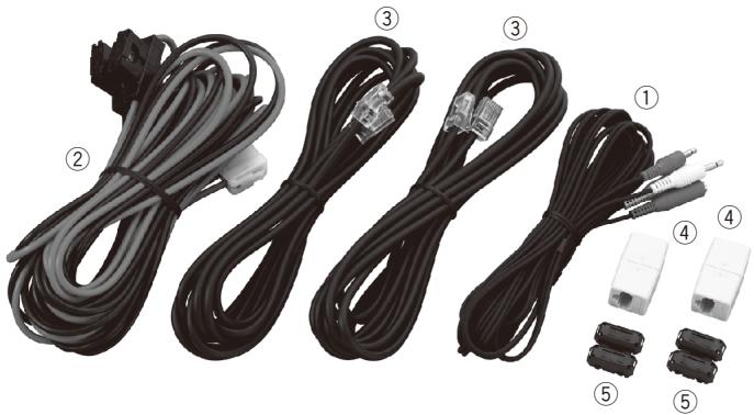
natural_image
Product photo of multiple black cable connectors with labeled parts, no visible text or symbolsPARTS LIST
| Ref. No. | New parts | Parts No. | Q'ty | Description |
| - | * | B62-2011-00 | 1 | INSTRUCTION MANUAL |
| 1 | E30-3399-05 | 1 | TRUNK CABLE (4m: SP) | |
| 2 | * | E30-3462-05 | 1 | DC CORD (6m) |
| 3 | * | E30-7639-05 | 2 | MODULAR CABLE (4m: MIC/PANEL) |
| 4 | * | E58-0525-15 | 2 | MODULAR JACK |
| - | G13-0978-04 | 1 | CUSHION | |
| - | J19-1433-05 | 2 | HOLDER | |
| 5 | L79-1417-05 | 2 | LINE FILTER | |
| - | N99-2016-15 | 1 | SCREW SET |
PG-5H (PC Interface Cable Kit (2 m))
■ External View
natural_image
Two black cables with connectors, labeled ① and ②, shown from different angles (no text or symbols on the cables themselves)PARTS LIST
| Ref. No. | New parts | Parts No. | Q'ty | Description |
| 1 | * | E30-7607-05 | 1 | PC cable (2m) |
| 2 | * | E30-7608-05 | 1 | Data cable (2m) |
MCP-2A (Memory Control Program)
To download the MCP-2A software, go to:
http://www.kenwood.com/i/products/info/amateur/
software_download.html
SPECIFICATIONS
| General | TM-D710A | TM-D710E | TM-D710A | |||
| K Type | E Type | M4 Type | ||||
| Guaranteed range | Band A & B | TX & RX | 144~148MHz | 144~146MHz | ||
| 438~450MHz | 430~440MHz | |||||
| Frequency range | Band A | RX | 118 ~ 524MHz | - | ||
| Band B | 136~524MHz | - | ||||
| 800~1300MHz (K type: excluding cellular band) | - | |||||
| Mode | F1D/ F2D/ F3E | |||||
| Antenna impedance | 50 Ω | |||||
| Operating temperature range | -20°C~+60°C (-4°F~+140°F) | |||||
| Power requirement | 13.8 V DC±15% (Negative ground) | |||||
| Frequency stability | Within ±5 ppm (-10°C~+50°C) | |||||
| Current | TX | VHF | HI | Less than 13.0A | - | |
| MID | Less than 5.5A | Less than 9.0A | ||||
| LOW | Less than 4.0A | |||||
| UHF | HI | Less than 13.0A | - | |||
| MID | Less than 6.5A | Less than 9.0A | ||||
| LOW | Less than 5.0A | |||||
| RX | Less than 1.2A (at 2W audio output) | |||||
| Dimensions(W x H x D) | Without projections | Operation panel: 155 x 70 x 38 mm (6.20" x 2.80" x 1.52") TX/RX unit: 140 x 43 x 142 mm (5.60" x 1.72" x 5.68") | ||||
| With projections | Operation panel: 156 x 71 x 56 mm (6.24" x 2.81" x 2.24") TX/RX unit: 140 x 44 x 158 mm (5.60" x 1.76" x 6.32") | |||||
| Weight (approx.) | Operation panel: 0.3 kg (0.66 lbs) TX/RX unit: 1.2 kg (2.64 lbs) | |||||
| Transmitter | ||||||
| RF power output | HI | 50W | - | |||
| MID | Approx. 10W | 25W | ||||
| LOW | Approx. 5W | |||||
| Modulation | Reactance modulation | |||||
| Maximum frequency deviation | Within ±5kHz | |||||
| Spurious radiation | Less than -60dB | |||||
| Modulation distortion (300Hz~3kHz) | Less than 3% | |||||
| Microphone impedance | 600Ω | |||||
| Receiver | ||||||
| Circuitry | Double super heterodyne | |||||
| Intermediate frequency | 1st (Band A/ Band B) | 45.05MHz/ 49.95MHz | ||||
| 2nd (Band A/ Band B) | 455kHz/ 450kHz | |||||
| Sensitivity (144, 430/ 440MHz band) | Less than 0.16μV | |||||
| Squelch sensitivity (144, 430/ 440MHz band) | Less than 0.1μV | |||||
| Selectivity | -6dB | More than 11kHz | ||||
| -50dB | Less than 30kHz | |||||
| Low frequency output (8Ω) | More than 2W (at 5% distortion) | |||||
SPECIFICATIONS
Sensitivity (approx.): excluding 144, 430/ 440MHz band
| Frequency range | Band A | Band B | |
| FM: 12dB SINAD | AM: 10dB S/N | FM: 12dB SINAD | |
| 118~135.995MHz | 0.32μV | 0.40μV | - |
| 136~173.995MHz | 0.32μV | 0.40μV | 0.32μV |
| 174~229.995MHz | 0.40μV | 0.50μV | 0.40μV |
| 230~299.995MHz | 5.6μV | 5.6μV | 5.6μV |
| 300~349.995MHz | 1.0μV | 1.0μV | 1.0μV |
| 350~399.995MHz | 0.56μV | 0.56μV | 0.56μV |
| 400~499.995MHz | 0.28μV | 0.36μV | 0.28μV |
| 500~523.995MHz | 0.56μV | 0.71μV | 0.56μV |
| 800~1239.99MHz | - | - | 7.08μV |
| 1240~1299.99MHz | - | - | 2.24μV |
Kenwood Corporation
2967-3, Ishikawa-machi, Hachioji-shi, Tokyo, 192-8525 Japan
Kenwood U.S.A. Corporation
P.O. BOX 22745, 2201 East Dominguez Street, Long Beach, CA 90801-5745, U.S.A.
Kenwood Electronics Canada Inc.
6070 Kestrel Road, Mississauga, Ontario, Canada L5T 1S8
Kenwood Electronics UK Limited
KENWOOD House, Dwight Road, Watford, Herts., WD18 9EB United Kingdom
Kenwood Electronics Europe B.V.
Amsterdamseweg 37, 1422 AC Uithoorn, The Netherlands
Kenwood Electronics Italia S.p.A.
Via G. Sirtori, 7/9 20129 Milano, Italy
Kenwood Ibérica, S.A.
Bolivia, 239-08020 Barcelona, Spain
Kenwood Electronics Australia Pty. Ltd.
(A.C.N. 001 499 074)
16 Giffnock Avenue, Centrecourt Estate, North Ryde, N.S.W. 2113 Australia
Kenwood Electronics (Hong Kong) Ltd.
Unit 3712-3724, Level 37, Tower one Metroplaza, 223 Hing Fong Road, Kwai Fong, N.T., Hong Kong
Kenwood Electronics Singapore Pte Ltd
1 Ang Mo Kio Street 63, Singapore 569110
TM-D710A/D710E PC BOARD
PC BOARD TM-D710A/D710E
DISPLAY UNIT (X54-3620-00) (A/4, B/4, C/4, D/4)
Component side view (J79-0141-09)
DISPLAY UNIT (X54-3620-00) (A/4, B/4, C/4, D/4)
Component side view (J79-0141-09)
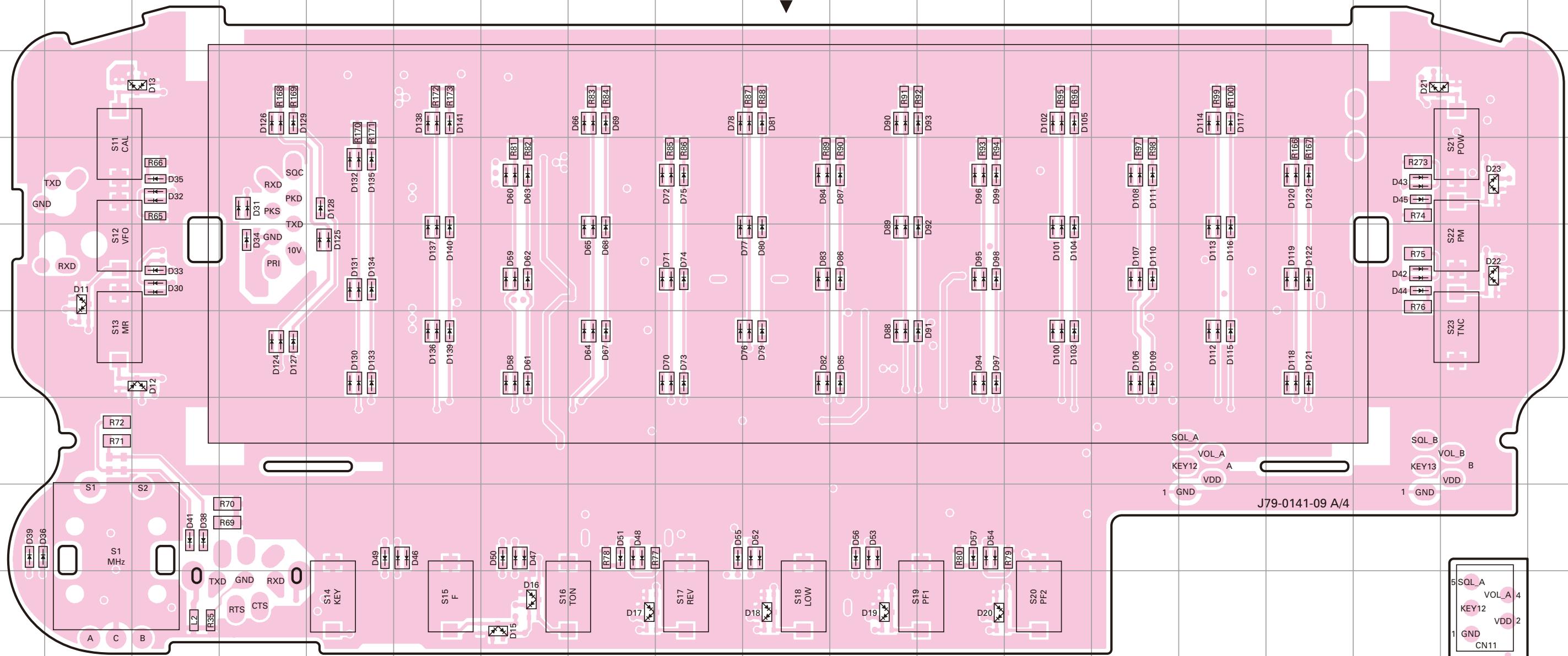
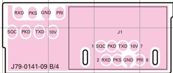
| Ref. No. | Address | Ref. No. | Address | Ref. No. | Address | Ref. No. | Address | Ref. No. | Address | Ref. No. | Address | Ref. No. | Address | Ref. No. | Address |
| D11 | 5B | D28 | 10R | D46 | 8F | D62 | 5G | D78 | 3J | D94 | 6L | D110 | 5N | D126 | 3D |
| D12 | 6C | D29 | 10R | D47 | 8G | D63 | 4G | D79 | 6J | D95 | 5L | D111 | 4N | D127 | 6D |
| D13 | 3C | D30 | 5C | D48 | 8H | D64 | 6H | D80 | 5J | D96 | 4L | D112 | 6O | D128 | 4E |
| D15 | 9G | D31 | 4D | D49 | 8E | D65 | 5H | D81 | 3J | D97 | 6L | D113 | 5O | D129 | 3D |
| D16 | 9G | D32 | 4C | D50 | 8G | D66 | 3H | D82 | 6J | D98 | 5L | D114 | 3O | D130 | 6E |
| D17 | 9H | D33 | 5C | D51 | 8H | D67 | 6H | D83 | 5J | D99 | 4L | D115 | 6O | D131 | 5E |
| D18 | 9J | D34 | 5D | D52 | 8H | D68 | 5H | D84 | 4J | D100 | 6M | D116 | 5O | D132 | 4E |
| D19 | 9K | D35 | 4C | D53 | 8K | D69 | 3H | D85 | 6K | D101 | 5M | D117 | 3O | D133 | 6E |
| D20 | 9L | D36 | 8A | D54 | 8L | D70 | 6I | D86 | 5K | D102 | 3M | D118 | 6P | D134 | 5E |
| D21 | 3Q | D38 | 8C | D55 | 8I | D71 | 5I | D87 | 4K | D103 | 6M | D119 | 5P | D135 | 4E |
| D22 | 5R | D39 | 8A | D56 | 8K | D72 | 4I | D88 | 6K | D104 | 5M | D120 | 4P | D136 | 6F |
| D23 | 4R | D41 | 8C | D57 | 8L | D73 | 6I | D89 | 5K | D105 | 3M | D121 | 6P | D137 | 5F |
| D24 | 13R | D42 | 5Q | D58 | 6G | D74 | 5I | D90 | 3K | D106 | 6N | D122 | 5P | D138 | 3F |
| D25 | 13R | D43 | 4Q | D59 | 5G | D75 | 4I | D91 | 6L | D107 | 5N | D123 | 4P | D139 | 6F |
| D26 | 13R | D44 | 5Q | D60 | 4G | D76 | 6J | D92 | 5L | D108 | 4N | D124 | 6D | D140 | 5F |
| D27 | 10R | D45 | 4Q | D61 | 6G | D77 | 5J | D93 | 3L | D109 | 6N | D125 | 5E | D141 | 3F |
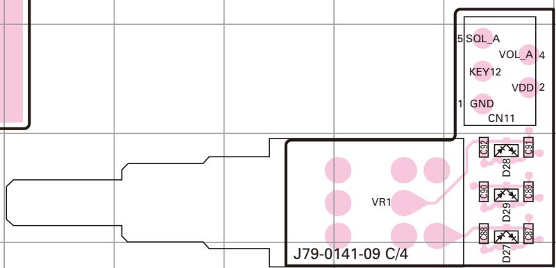
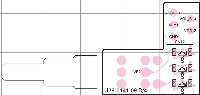
TM-D710A/D710E PC BOARD
PC BOARD TM-D710A/D710E
DISPLAY UNIT (X54-3620-00) (A/4, B/4, C/4, D/4)
Foil side view (J79-0141-09)
DISPLAY UNIT (X54-3620-00) (A/4, B/4, C/4, D/4)
Foil side view (J79-0141-09)
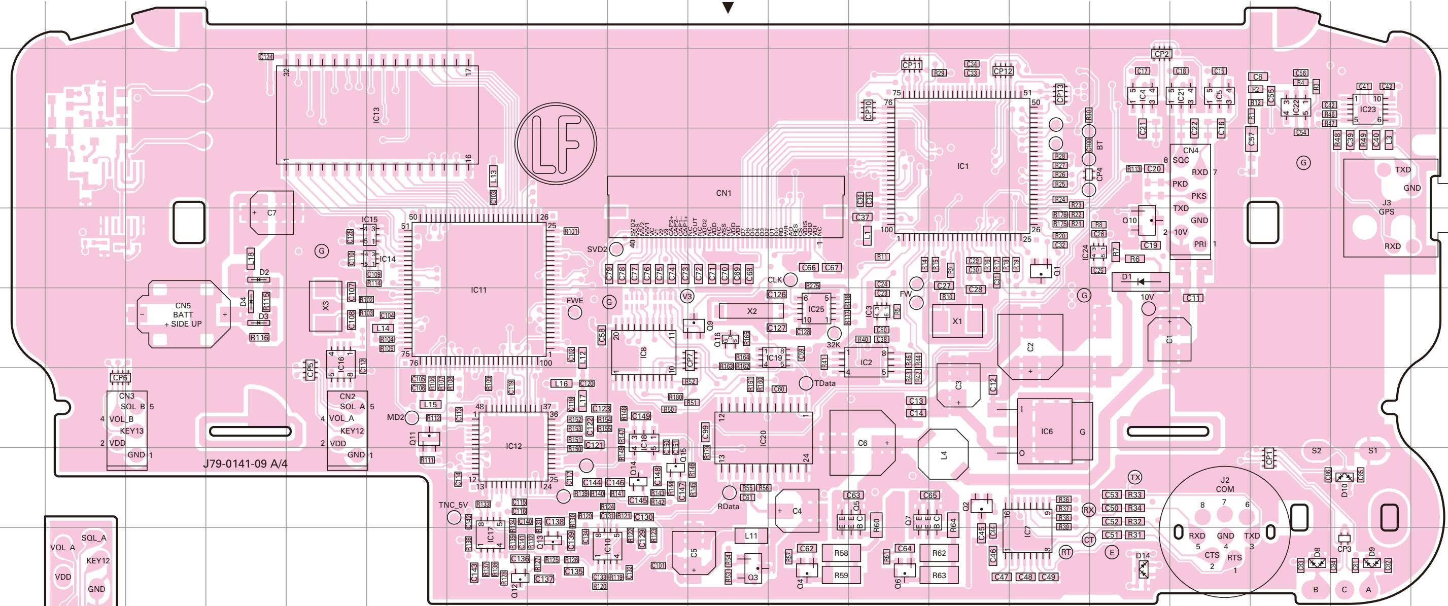
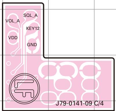
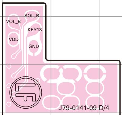
| Ref. No. | Address | Ref. No. | Address | Ref. No. | Address | Ref. No. | Address |
| IC1 | 4M | IC16 | 6E | Q5 | 8L | D4 | 6D |
| IC2 | 6L | IC17 | 9G | Q6 | 9L | D8 | 9Q |
| IC3 | 6L | IC18 | 7I | Q7 | 8L | D9 | 9R |
| IC4 | 3O | IC19 | 6K | Q9 | 6J | D10 | 8R |
| IC5 | 3P | IC20 | 7J | Q10 | 5O | D14 | 9O |
| IC6 | 7N | IC21 | 3P | Q11 | 7F | ||
| IC7 | 9N | IC22 | 3Q | Q12 | 9G | ||
| IC8 | 6I | IC23 | 3R | Q13 | 9H | ||
| IC10 | 9I | IC24 | 5O | Q14 | 8I | ||
| IC11 | 6G | IC25 | 6K | Q15 | 8I | ||
| IC12 | 7G | Q1 | 5N | Q16 | 6J | ||
| IC13 | 3F | Q2 | 8M | D1 | 5O | ||
| IC14 | 5F | Q3 | 9J | D2 | 5D | ||
| IC15 | 5F | Q4 | 9K | D3 | 6D |
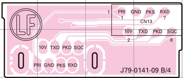
TM-D710A/D710E PC BOARD
PC BOARD TM-D710A/D710E
TX-RX UNIT
(X57-731X-XX)(A/6):
TX-RX SECTION
0-11: K 0-21: M4 2-71: E
Component side view
(J79-0142-19 A/6)
| Ref. No. | Address | Ref. No. | Address |
| D188 | 12N | D361 | 6I |
| D189 | 9M | D362 | 9G |
| D190 | 10I | D363 | 9H |
| D191 | 11P | D364 | 9I |
| D192 | 13O | D365 | 9I |
| D193 | 10J | D367 | 9I |
| D226 | 6I | D368 | 9I |
| D227 | 12G | D370 | 9J |
| D229 | 12I | D371 | 9J |
| D230 | 12I | D375 | 9K |
| D231 | 12I | D376 | 9K |
| D232 | 13I | D377 | 9K |
| D233 | 13J | D378 | 9K |
| D234 | 13J | D379 | 9K |
| D238 | 13K | D406 | 6H |
| D239 | 12K | D407 | 7G |
| D240 | 12K | D408 | 7H |
| D241 | 12L | D409 | 8I |
| D242 | 12L | D410 | 8I |
| D243 | 12L | D412 | 8I |
| D291 | 6H | D413 | 8I |
| D292 | 11G | D415 | 8J |
| D294 | 11I | D416 | 8J |
| D295 | 11I | D419 | 8K |
| D296 | 11I | D420 | 8K |
| D297 | 12I | D421 | 8J |
| D298 | 12J | D423 | 8K |
| D299 | 12J | D424 | 8K |
| D303 | 12K | D451 | 9M |
| D304 | 12K | D456 | 6H |
| D305 | 12K | D457 | 7G |
| D306 | 11K | D489 | 3K |
| D307 | 11L | D610 | 4M |
| D308 | 11L | D612 | 3M |
| D356 | 12M |
Component side
| Layer 1 | |
| Layer 2 | |
| Layer 3 | |
| Layer 4 | |
| Foil side | |
TM-D710A/D710E PC BOARD
PC BOARD TM-D710A/D710E
TX-RX UNIT
(X57-731X-XX)(A/6):
TX-RX SECTION
TX-RX UNIT (B/6) : VCO A SECTION
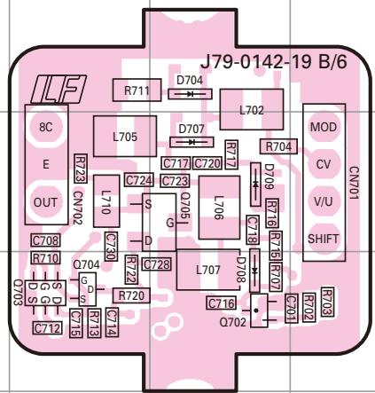
TX-RX UNIT (E/6) : VCO A SECTION
| Ref. No. | Address | Ref. No. | Address | Ref. No. | Address | Ref. No. | Address |
| IC801 | 4H | Q704 | 13H | Q808 | 5P | D708 | 13I |
| IC802 | 7O | Q705 | 12I | Q809 | 6O | D709 | 12I |
| IC803 | 5O | Q752 | 13F | Q810 | 7J | D754 | 11F |
| IC804 | 8M | Q753 | 13E | Q811 | 7K | D757 | 12F |
| IC805 | 8J | Q754 | 13E | Q812 | 6N | D758 | 13F |
| IC806 | 6M | Q755 | 12F | Q816 | 7H | D759 | 12F |
| IC807 | 8N | Q801 | 7N | Q817 | 9M | D801 | 8N |
| IC951 | 3O | Q803 | 7I | Q951 | 8H | D802 | 8O |
| IC952 | 4L | Q804 | 6J | Q953 | 8H | D954 | 5P |
| IC953 | 8I | Q805 | 5P | Q955 | 5M | D956 | 5M |
| Q702 | 13I | Q806 | 6J | D704 | 11I | D957 | 9H |
| Q703 | 13H | Q807 | 6K | D707 | 12I |
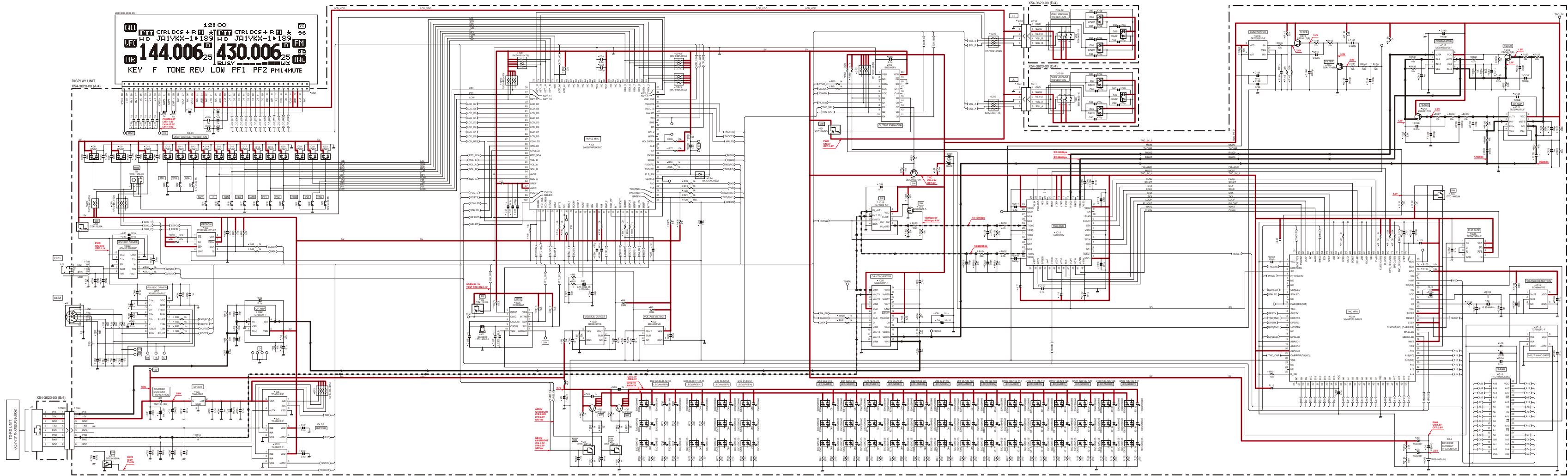
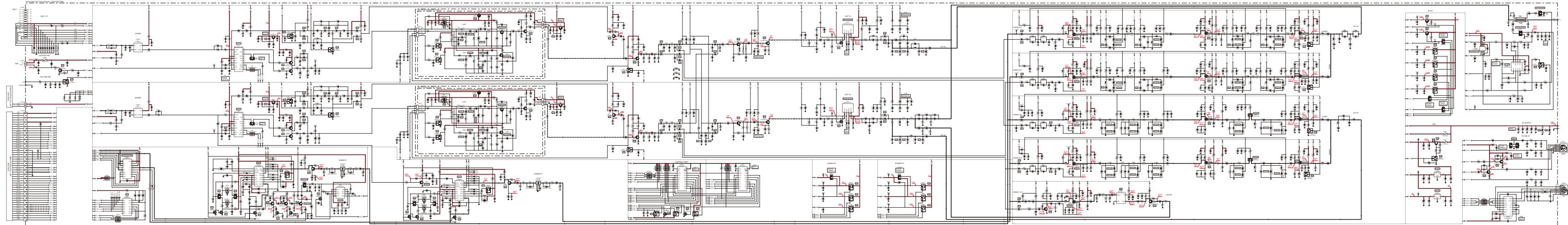
flowchart
graph TD
    A["Power Supply"] --> B["Component 1"]
    B --> C["Component 2"]
    C --> D["Component 3"]
    D --> E["Component 4"]
    E --> F["Output"]
    style A fill:#f9f,stroke:#333
    style B fill:#ccf,stroke:#333
    style C fill:#cfc,stroke:#333
    style D fill:#fcc,stroke:#333
    style E fill:#cff,stroke:#333
    style F fill:#ffc,stroke:#333
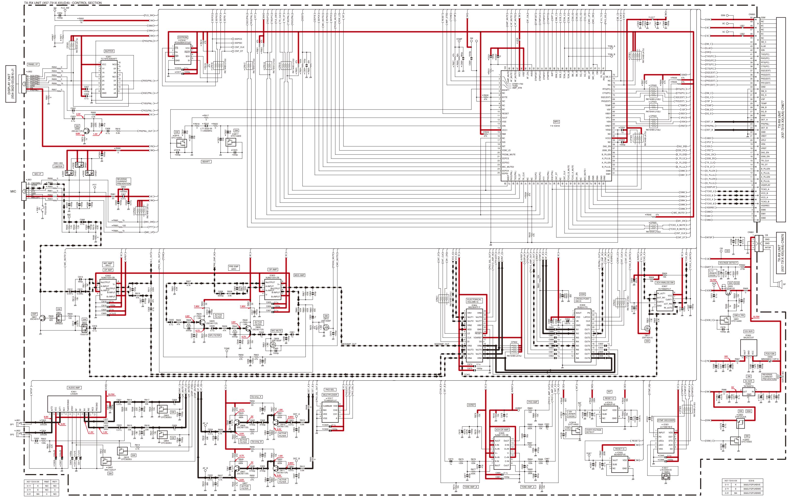
| X57-731X-XX | IC918 | |
| 0-11 | K | 3062LFGPUKBVE |
| 2-71 | E | 3062LFGPUKBWE |
| 0-21 | M4 | 3062LFGPUKBWE |
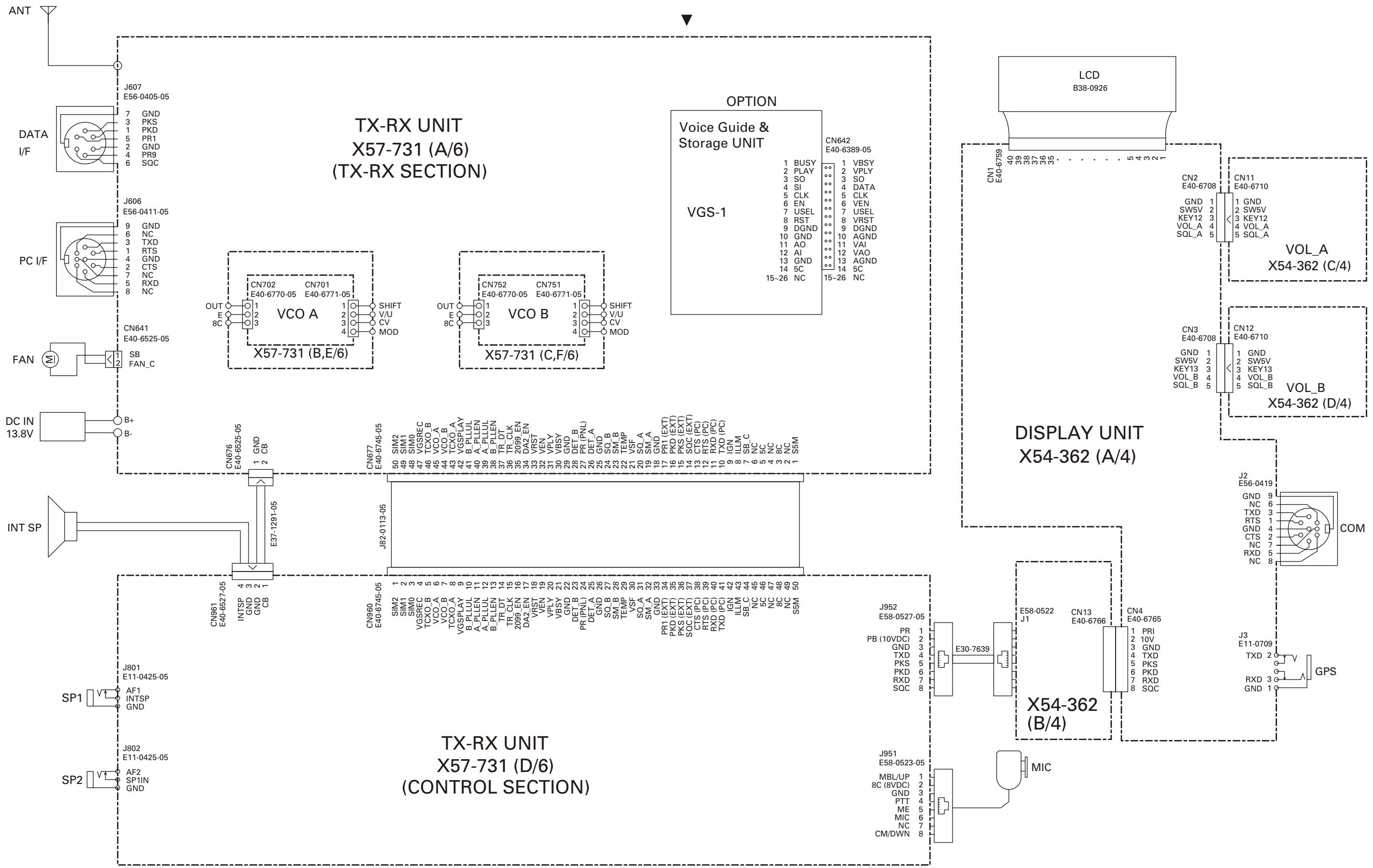
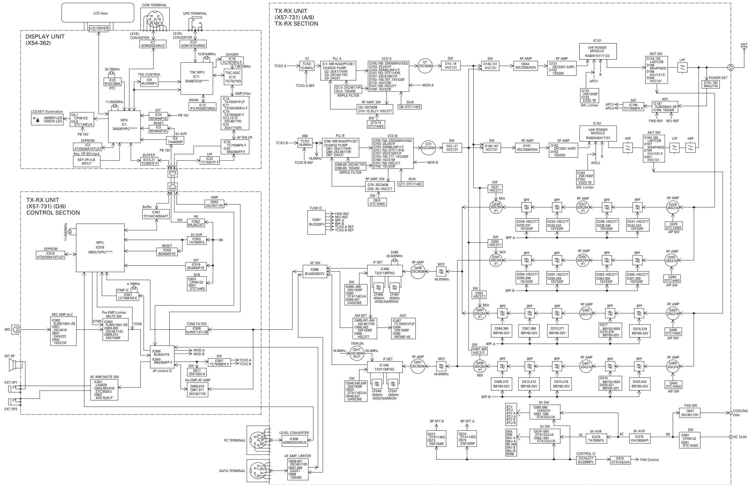
flowchart
graph TD
    subgraph Display Unit (X54-362)
        A["CDL ASy"] --> B["COM TERMINAL"]
        B --> C["ICD0002EARUZ"]
        C --> D["IC30DM10ARMZ"]
        D --> E["IC2BVC386A"]
        E --> F["TNC CONTROL"]
        F --> G["IC113048T2E2****"]
        G --> H["TNC MPU IC11"]
        H --> I["IC12T070190"]
        I --> J["AMP Filter"]
        J --> K["AMP"]
        K --> L["MPU IC130626FPG****"]
        L --> M["INT"]
        M --> N["IC24BD4849VE"]
        N --> O["RESET"]
        O --> P["IC3RD4840FVE"]
        P --> Q["IF 10V"]
        Q --> R["IF 5V AVR"]
        R --> S["IF 10V"]
        S --> T["IF 5V AVR"]
        T --> U["IF 5V AVR"]
        U --> V["IF 5V AVR"]
        V --> W["IF 5V AVR"]
        W --> X["IF 5V AVR"]
        X --> Y["IF 5V AVR"]
        Y --> Z["IF 5V AVR"]
        Z --> AA["IF 5V AVR"]
        AA --> AB["IF 5V AVR"]
        AB --> AC["IF 5V AVR"]
        AC --> AD["IF 5V AVR"]
        AD --> AE["IF 5V AVR"]
        AE --> AF["IF 5V AVR"]
        AF --> AG["IF 5V AVR"]
        AG --> AH["IF 5V AVR"]
        AH --> AI["IF 5V AVR"]
        AI --> AJ["IF 5V AVR"]
        AJ --> AK["IF 5V AVR"]
        AK --> AL["IF 5V AVR"]
        AL --> AM["IF 5V AVR"]
        AM --> AN["IF 5V AVR"]
        AN --> AO["IF 5V AVR"]
        AO --> AP["IF 5V AVR"]
        AP --> AQ["IF 5V AVR"]
        AQ --> AR["IF 5V AVR"]
        AR --> AS["IF 5V AVR"]
        AS --> AT["IF 5V AVR"]
        AT --> AU["IF 5V AVR"]
        AU --> AV["IF 5V AVR"]
        AV --> AW["IF 5V AVR"]
        AW --> AX["IF 5V AVR"]
        AX --> AY["IF 5V AVR"]
        AY --> AZ["IF 5V AVR"]
        AZ --> BA["IF 5V AVR"]
        BA --> BB["IF 5V AVR"]
        BB --> BC["IF 5V AVR"]
        BC --> BD["IF 5V AVR"]
        BD --> BE["IF 5V AVR"]
        BE --> BF["IF 5V AVR"]
        BF --> BG["IF 5V AVR"]
        BG --> BH["IF 5V AVR"]
        BH --> BI["IF 5V AVR"]
        BI --> BJ["IF 5V AVR"]
        BJ --> BK["IF 5V AVR"]
        BK --> BL["IF 5V AVR"]
        BL --> BM["IF 5V AVR"]
        BM --> BN["IF 5V AVR"]
        BN --> BO["IF 5V AVR"]
        BO --> BP["IF 5V AVR"]
        BP --> BQ["IF 5V AVR"]
        BQ --> BR["IF 5V AVR"]
        BR --> BS["IF 5V AVR"]
        BS --> BT["IF 5V AVR"]
        BT --> BU["IF 5V AVR"]
        BU --> BV["IF 5V AVR"]
        BV --> BW["IF 5V AVR"]
        BW --> BX["IF 5V AVR"]
        BX --> BY["IF 5V AVR"]
        BY --> BZ["IF 5V AVR"]
        BZ --> CA["IF 5V AVR"]
        CA --> CB["IF 5V AVR"]
        CB --> CC["IF 5V AVR"]
        CC --> CD["IF 5V AVR"]
        CD --> CE["IF 5V AVR"]
        CE --> CF["IF 5V AVR"]
        CF --> CG["IF 5V AVR"]
        CG --> CH["IF 5V AVR"]
        CH --> CI["IF 5V AVR"]
        CI --> CJ["IF 5V AVR"]
        CJ --> CK["IF 5V AVR"]
        CK --> CL["IF 5V AVR"]
        CL --> CM["IF 5V AVR"]
        CM --> CN["IF 5V AVR"]
        CN --> CO["IF 5V AVR"]
        CO --> CP["IF 5V AVR"]
        CP --> CQ["IF 5V AVR"]
        CQ --> CR["IF 5V AVR"]
        CR --> CS["IF 5V AVR"]
        CS --> CT["IF 5V AVR"]
        CT --> CU["IF 5V AVR"]
        CU --> CV["IF 5V AVR"]
        CV --> CW["IF 5V AVR"]
    end

    subgraph Display Unit (X54-362)
        D1CCK0A
    end

    subgraph TX-RX UNIT (X57-731) (A/6) TX-RX SECTION
    E1CCK0A
    E2CCK0A
    E3CCK0A
    E4CCK0A
    E5CCK0A
    E6CCK0A
    E7CCK0A
    E8CCK0A
    E9CCK0A
    E10CCK0A
    E11CCK0A
    E12CCK0A
    E13CCK0A
    E14CCK0A
    E15CCK0A
    E16CCK0A
    E17CCK0A
    E18CCK0A
    E19CCK0A
    E20CCK0A
    E21CCK0A
    E22CCK0A
    E23CCK0A
    E24CCK0A
    E25CCK0A
    E26CCK0A
    E27CCK0A
    E28CCK0A
    E29CCK0A
    E30CCK0A
    E31CCK0A
    E32CCK0A
    E33CCK0A
    E34CCK0A
    E35CCK0A
    E36CCK0A
    E37CCK0A
    E38CCK0A
    E39CCK0A
    E40CCK0A
    E41CCK0A
    E42CCK0A
    E43CCK0A
    E44CCK0A
    E45CCK0A
    E46CCK0A
    E47CCK0A
    E48CCK0A
    E49CCK0A
    E50CCK0A
    E51CCK0A
    E52CCK0A
    E53CCK0A
    E54CCK0A
    E55CCK0A
    E56CCK0A
    E57CCK0A
    E58CCK0A
    E59CCK0A
    E60CCK0A
    E61CCK0A
    E62CCK0A
    E63CCK0A
    E64CCK0A
    E65CCK0A
    E66CCK0A
    E67CCK0A
    E68CCK0A
    E69CCK0A
    E70CCK0A
    E71CCK0A
    E72CCK0A
    E73CCK0A
    E74CCK0A
    E75CCK0A
    E76CCK0A
    E77CCK0A
    E78CCK0A
    E79CCK0A
    E80CCK0A
    E81CCK0A
    E82CCK0A
    E83CCK0A
    E84CCK0A
    E85CCK0A
    E86CCK0A
    E87CCK0A
    E88CCK0A
    E89CCK0A
    E90CCK0A
    E91CCK0A
    E92CCK0A
    E93CCK0A
    E94CCK0A
    E95CCK0A
    E96CCK0A
    E97CCK0A
    E98CCK0A
    E99CCK0A
    FWH REF REV REF

    subgraph Control Section (TX-RX UNIT)
        MPU_IC18_3062LFGPU*****
        MPU_IC18_3062LFGPU*****
        MPU_IC18_3062LFGPU*****
        MPU_IC18_3062LFGPU*****
        MPU_IC18_3062LFGPU*****
        MPU_IC18_3062LFGPU*****
        MPU_IC18_3062LFGPU*****
        MPU_TCP_17_4HC17_4HC17_4HC17_4HC17_4HC17_4HC17_4HC17_4HC17_4HC17_4HC17_4HC17_4HC17_4HC17_4HC17_4HC17_4HC17_4HC17_4HC17_4HC17_4HC17_4HG17_4HG17_4HG17_4HG17_4HG17_4HG17_4HG17_4HG17_4HG17_4HG17_4HG17_4HG17_4HG17_4HG17_4HG17_4HG17_4HG17_4HG17_4HG17_4HG17_4HWHWHEHTHEATHEATHEATHEATHEATHEATHEATHEATHEATHEATHEATHEATHEATHEATHEATHEATHEATHEATHEATHEATHEATHEATHEATHEATHEATHEATHEATHEATHEATHEATHEATHEATHEATHEATHEATHEATHEATHEATHEATHEATHEATHEATHEATHEATHEATHEATHEATHEATHEATHEATHEATTHEATTHEATHEATTHEATTHEATTHEATTHEATTHEATTHEATTHEATTHEATTHEATTHEATTHEATTHEATTHEATTHEATTHEATTHEATTHEATTHEATTHEATTHEATTHEATTHEATTHEATTHEATTHEATTHEATTHEATTHEATTHEATTHEATTHEATTHEATTHEATTHEATTHEATTHEATTHEATTHEATTHEATTHEATTHEATTHEATTHEATTHEATTHEATTHEATTHEATTHEATTHEATTHEAT THEAT THEAT THE AT THE AT THE AT THE AT THE AT THE AT THE AT THE AT THE AT THE AT THE AT THE AT THE AT THE AT THE AT THE AT THE AT THE AT THE AT THE AT THE AT THE AT THE AT THE AT THE AT THE AT THE AT THE AT THE AT THE AT THE AT THE AT THE AT THE AT THE AT THE AT THE AT THE AT THE AT THE AT THE AT THE AT THE AT THE AT THE AT THE AT THE AT THE AT THE AT THE AT THE TATE OF THIS TATE OF THIS TATE OF THIS TATE OF THIS TATE OF THIS TATE OF THIS TATE OF THIS TATE OF THIS TATE OF THIS TATE OF THIS TATE OF THIS TATE OF THIS TATE OF THIS TATE OF THIS TATE OF THIS TATE OF THIS TATE OF THIS TATE OF THIS TATE OF THIS TATE OF THIS TATE OF THIS TATE OF THIS TATE OF THIS TATE OF THIS TATE OF THIS TATE OF This TATE OF THIS TATE OF THIS TATE OF THIS TATE OF THIS TATE OF THIS TATE OF THIS TATE OF THIS TATE OF THIS TATE OF THIS TATE OF THIS TATE OF THIS TATE OF THIS TATE OF THIS TATE OF THIS TATE OF THIS TATE OF THIS TATE OF THIS TATE OF THIS TATE OF THIS TATE OF THIS TATE OF THIS TATE OF THIS TATE OF THIS TATE OF THIS TATE OF \STB\STB\STB\STB\STB\STB\STB\STB\STB\STB\STB\STB\STB\STB\STB\STB\STB\STB\STB\STB\STB\STB\STB\STB\STB\STB\STB\STB\STB\STB\STB\STB\STB\STB\STB\STB\STB\STB\STB\STB\STB\STB\STB\STB\STB\STB\STB\STB\STB\STB\STB\STB\STB\STB\STB\STB\STB\STB\STB\STB\STB\STB\STB\STB\STB\ STB\STB\ STB\STB\ STB\STB\ STB\STB\ STB\STB\ STB\STB\ STB\STB\ STB\STB\ STB\STB\ STB\STB\ STB\STB\ STB\STB\ STB\STB\ STB\STB\ STBSTB STBSTB STBSTB STBSTB STBSTB STBSTB STBSTB STBSTB STBSTB STBSTB STBSTB STBSTB STBSTB STBSTB STBSTB STBSTB STBSTB SFT B & SFT A & SFT B & SFT A & SFT B & SFT A & SFT B & SFT A & SFT B & SFT A & SFT B & SFT A & SFT B & SFT A & SFT B & SFT A & SFT B & SFT A & SFT B & SFT A & SFT B & SFT A & SFT B & SFT A & SFT B & SFT A & SFT B& SFT B & SFT A & SFT B & SFT A & SFT B & SFT A & SFT B & SFT A & SFT B & SFT A & SFT B & SFT A & SFT B & SFT A & SFT B & SFT A & SFT B & SFT A & SFT B & SFT A & SFT B & SFT A & SFT B & SFT A & SFT B &
      subgraph Control Section (TX-RX UNIT)
            MPU_IC18_3062LFGPU*****
            MPU_IC18_3062LFGPU*****
            MPU_IC18_3062LFGPU*****
            MPU_IC18_3062LFGPU*****
            MPU_IC18_3062LFGPU*****
            MPU_IC18_3062LFGPU*****
            MPU_IC18_3062LFGPU*****
            MPU_TCP_17_4HC17_4HC17_4HC17_4HC17_4HC17_4HC17_4HC17_4HC17_4HC17_4HC17_4HC17_4HC17_4HC17_4HC17_4HC17_4HC17_4HC17_4HC17_4HGCLTCCDCDCDCDCDCDCDCDCDCDCDCDCDCDCDCDCDCDCDCDCDCDCDCDCDCDCDCDCDCDCDCDCDCDCDCDCDCDCDCDCDCDCDCDCDCDCDCDCDCDCDCDCDCDCDCDCDCDCDCDCDCDCDCDCDCDCDCDCDCDCDCDCDCDCDCDCDCDCDCDCDCDCDCDCDCDCDCDCDCDCDCDCDCDCDCDCDCDCDCDCDCCDDCCDDCCDDCCDDCCDDCCDDCCDDCCDDCCDDCCDDCCDDCCDDCCDDCCDDCCDDCCDDCCDDCCDDCCDDCCDDCCDDCCDDCCDDCCDDCCDDCCDDCCDDCCDDCCDDCCDDCCDDCCDDCCDDCCDDCCDDCCDDCCDDCCDDCCDDCCDDCCDDCCDDCCDDCCDDCCDDCCDDCCDDCCDDCCDDCCDDCCDCCDDCCDDCCDDCCDDCCDDCCDDCCDDCCDDCCDDCCDDCCDDCCDDCCDDCCDDCCDDCCDDCCDDCCDDCCDDCCDDCCDDCCDDCCDDCCDDCCDDCCDDCCDDCCDDCCDDCCDDCCDDCCDDCCDDCCDDCCDDCCDDCCDDCCDDCCDDCCDDCCDDCCDDCCDDCCDDCCDDCCDDCCDDCCDDCCDDCCC DSSDSCCHDSSDSCCHDSSDSCCHDSSDSCCHDSSDSCCHDSSDSCCHDSSDSCCHDSSDSCCHDSSDSCCHDSSDSCCHDSSDSCCHDSSDSCCHDSSDSCCHDSSDSCCHDSSDSCCHDSSDSCCHDSSDSCCHDSSDSCCHDSSDSCCHDSSDSCCHDSSDSCCHHDSBCGDSBCGDSBCGDSBCGDSBCGDSBCGDSBCGDSBCGDSBCGDSBCGDSBCGDSBCGDSBCGDSBCGDSBCGDSBCGDSBCGDSBCGDSBCGDSBCGDSBCGDSBCGDSBCGDSBCGDSBCGDSBCGDSBCGDSBCGDSBCGDSBCGDSBCGDSBCGDSBCGDSBCGGSDSBCGDSBCGDSBCGDSBCGDSBCGDSBCGDSBCGDSBCGDSBCGDSBCGDSBCGDSBCGDSBCGDSBCGDSBCGDSBCGDSBCGDSBCGDSBCGDSBCGDSBCGDSBCGDSBCGDSBCGDSBCGDSBCGDSBCGDSBCGDSBCGDSBCGDSBCGDSBCGDSBCGTSDSBCGSDSBCGSDSBCGSDSBCGSDSBCGSDSBCGSDSBCGSDSBCGSDSBCGSDSBCGSDSBCGSDSBCGSDSBCGSDSBCGSDSBCGSDSBCGSDSBCGSDSBCGSDSBCGSDSBCGSDSBCGSDSBCGSDSBCGSDSBCGSDSBCGSDSBCGSDSBCGSDSBCGSDSBCGSDSBCGSDSBCGSDSBCGSDSBCGSDSBCGSMSHSHSHSHSHSHSHSHSHSHSHSHSHSHSHSHSHSHSHSHSHSHSHSHSHSHSHSHSHSHSHSHSHSHSHSHSHSHSHSHSHSHSHSHSHSHSHSHSHSHSHSHSHSHSHSHSHSHSHSHSHSHSHSHSHSHSHSHSHSHSHSHSHSHSHSHSHSHSHSHSHSHSHSHSHSHSHSHSHSHSHSHSHSHSHSHSHHSHTSHTSHTSHTSHTSHTSHTSHTSHTSHTSHTSHTSHTSHTSHTSHTSHTSHTSHTSHTSHTSHTSHTSHTSHTSHTSHTSHTSHTSHTSHTSHTSHTSHTSHTSHTSHTSHTSHTSHTSHTSHTSHTSHTSHTSHTSHTSHTSHTSHTS HTTTTGTGTGTGTGTGTGTGTGTGTGTGTGTGTGTGTGTGTGTGTGTGTGTGTGTGTGTGTGTGTGTGTGTGTGTGTGTGTGTGTGTGTGTGTGTGTGTGTGTGTGTGTGTGTGTGTGTGTGTGTGTGTGTGTGTGTGTGTGTGTGTGTGTGTGTGTGTGTGTGTGTGTGTGTGTGTGTGTGTGTGTGTGTGTGTGTGTGTGTGTgttTMTMTCNMDIINOLVDIIGTDNIDNIDNIDNIDNIDNIDNIDNIDNIDNIDNIDNIDNIDNIDNIDNIDNIDNIDNIDNIDNIDNIDNIDNIDNIDNIDNIDNIDNIDNIDNIDNIDNIDNIDNIDNIDNIDNIDNIDNIDNIDNIDNIDNIDNIDNIDNIDNIDNIDNIDNINODINODINODINODINODINODINODINODINODINODINODINODINODINODINODINODINODINODINODINODINODINODINODINODINODINODINODINODINODINODINODINODINODINODINODINODINODINODINODINODINODINODINODINODINODINODINODINODINODINODINONOIOIOIOIOIOIOIOIOIOIOIOIOIOIOIOIOIOIOIOIOIOIOIOIOIOIOIOIOIOIOIOIOIOIOIOIOIOIOIOIOIOIOIOIOIOIOIOIOIOIOIOIOIOIOIOIOIOIOIOIOIOIOIOIOIOIOIOIOIOIOIOIOIOIOIOIOIOIOIOIOIOIOIOIOIOIOIOIOIOIOIOIOIOIOIOIOIOIOIOIO IOVAIAIAIAIAIAIAIAIAIAIAIAIAIAIAIAIAIAIAIAIAIAIAIAIAIAIAIAIAIAIAIAIAIAIAIAIAIAIAIAIAIAIAIAIAIAIAIAIAIAIAIAIAIAIAIAIAIAIAIAIAIAIAIAIAIAIAIAIAIAIAIAIAIAIAIAIAIAIAIAIAIAIAIAIAIAIAIAIAIAIAIAIAIAIAIAIAIAIAIAIAIIAAIIAAIIAAIIAAIIAAIIAAIIAAIIAAIIAAIIAAIIAAIIAAIIAAIIAAIIAAIIAAIIAAIIAAIIAAIIAAIIAAIIAAIIAAIIAAIIAAIIAAIIAAIIAAIIAAIIAAIIAAIIAAIIAAIIAAIIAAIIAAIIAAIIAAIIAAIIAAIIAAIIAAIIAAIIAAIIAAIIAAIIAAIIAAIIAAIIAAIIAAA<nl>

