
B450M PRO-VDH V2 - Wall socket MSI - Free user manual and instructions
Find the device manual for free B450M PRO-VDH V2 MSI in PDF.

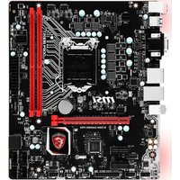
| Product type | Motherboard for PC |
| Brand | MSI |
| Model | B450M PRO-VDH V2 |
| Form factor | micro-ATX |
| Dimensions | 24.4 cm x 24.4 cm |
| Socket | AM4 |
| Chipset | AMD B450 |
| CPU support | AMD Ryzen 1st/2nd generation, Ryzen with Radeon Vega graphics, Athlon with Radeon Vega graphics |
| Memory | 4 x DDR4 DIMM, up to 64 GB, 1866-3466 MHz (OC) |
| Expansion slots | 1x PCIe 3.0 x16, 2x PCIe 2.0 x1 |
| Storage | 4x SATA 6 Gb/s, 1x M.2 (PCIe 3.0 x4/x2 and SATA) |
| Rear USB | 4x USB 3.1 Gen1, 4x USB 2.0 |
| Internal USB | 2x USB 3.1 Gen1, 4x USB 2.0 |
| Video outputs | 1x VGA, 1x DVI-D, 1x HDMI 1.4 |
| Audio | Realtek ALC892, 7.1 channels |
| Network | Realtek 8111H Gigabit LAN |
| Power supply | 1x 24-pin ATX, 1x 8-pin ATX 12V |
| BIOS | 128 Mb UEFI AMI, ACPI 6.1 |
| Internal connectors | USB, fans (CPU + 2 system), audio, front panel, TPM, chassis intrusion, serial, parallel, RGB |
| Included software | MSI APP MANAGER, COMMAND CENTER, LIVE UPDATE, MYSTIC LIGHT, etc. |
| Max temperature | 60°C |
| Maintenance | Clean with a dry cloth, avoid moisture |
Frequently Asked Questions - B450M PRO-VDH V2 MSI
User questions about B450M PRO-VDH V2 MSI
0 question about this device. Answer the ones you know or ask your own.
Ask a new question about this device
Download the instructions for your Wall socket in PDF format for free! Find your manual B450M PRO-VDH V2 - MSI and take your electronic device back in hand. On this page are published all the documents necessary for the use of your device. B450M PRO-VDH V2 by MSI.
USER MANUAL B450M PRO-VDH V2 MSI
Thank you for purchasing the MSI® B450M PRO-VDH V2 motherboard. This User Guide gives information about board layout, component overview, BIOS setup and software installation.
Contents
Safety Information....2
Specifications....3
Package contents 5
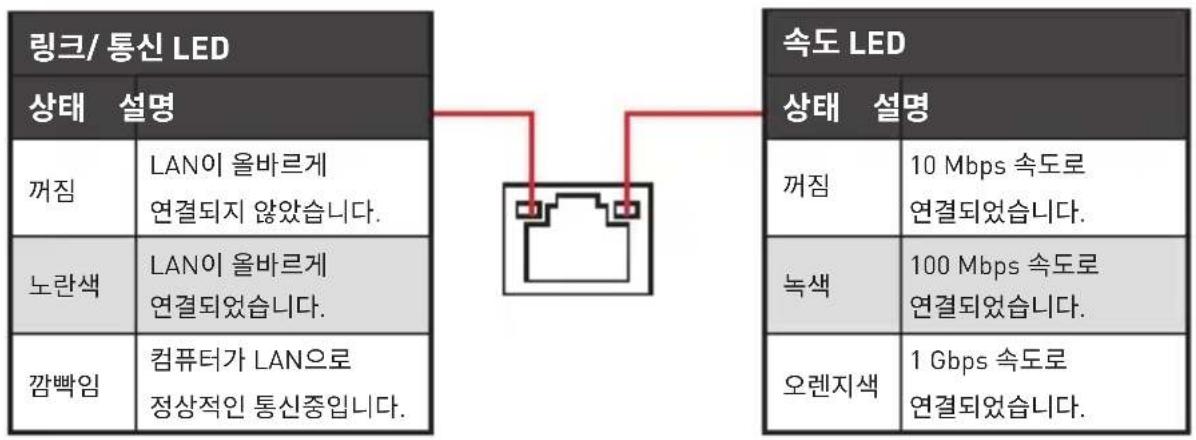
Rear I/O Panel 6
LAN Port LED Status Table....6
Overview of Components 7
CPU Socket 8
DIMM Slots....9
PCI_E1\~3: PCIe Expansion Slots....10
JFP1, JFP2: Front Panel Connectors 11
SATA1\~4: SATA 6Gb/s Connectors....11
M2_1: M.2 Slot (Key M) 12
ATX_PWR1, CPU_PWR1: Power Connectors....12
JUSB1\~2: USB 2.0 Connectors....13
JUSB3: USB 3.1 Gen1 Connector ....13
CPU_FAN1, SYS_FAN1\~2: Fan Connectors....14
JTPM1: TPM Module Connector 15
JCI1: Chassis Intrusion Connector....15
JAUD1: Front Audio Connector....16
JCOM1: Serial Port Connector 16
JLPT1: Parallel Port Connector....16
JBAT1: Clear CMOS (Reset BIOS) Jumper 17
EZ Debug LED: Debug LED indicators....17
JRGB1: RGB LED strip connector....17
BIOS Setup 18
Entering BIOS Setup....18
Resetting BIOS....19
Updating BIOS....19
Software Description....20
Installing Windows ^® 10....20
Installing Drivers ....20
Installing Utilities....20
Safety Information
- The components included in this package are prone to damage from electrostatic discharge (ESD). Please adhere to the following instructions to ensure successful computer assembly.
- Ensure that all components are securely connected. Loose connections may cause the computer to not recognize a component or fail to start.
- Hold the motherboard by the edges to avoid touching sensitive components.
- It is recommended to wear an electrostatic discharge (ESD) wrist strap when handling the motherboard to prevent electrostatic damage. If an ESD wrist strap is not available, discharge yourself of static electricity by touching another metal object before handling the motherboard.
- Store the motherboard in an electrostatic shielding container or on an anti-static pad whenever the motherboard is not installed.
- Before turning on the computer, ensure that there are no loose screws or metal components on the motherboard or anywhere within the computer case.
- Do not boot the computer before installation is completed. This could cause permanent damage to the components as well as injury to the user.
- If you need help during any installation step, please consult a certified computer technician.
- Always turn off the power supply and unplug the power cord from the power outlet before installing or removing any computer component.
- Keep this user guide for future reference.
- Keep this motherboard away from humidity.
- Make sure that your electrical outlet provides the same voltage as is indicated on the PSU, before connecting the PSU to the electrical outlet.
- Place the power cord such a way that people can not step on it. Do not place anything over the power cord.
- All cautions and warnings on the motherboard should be noted.
- If any of the following situations arises, get the motherboard checked by service personnel:
- Liquid has penetrated into the computer.
■ The motherboard has been exposed to moisture.
- The motherboard does not work well or you can not get it work according to user guide.
■ The motherboard has been dropped and damaged.
■ The motherboard has obvious sign of breakage.
- Do not leave this motherboard in an environment above 60^ (140°F), it may damage the motherboard.
Specifications
| CPU | Supports AMD® Ryzen 1st and 2nd Generation/ RyzenTM with RadeonTM Vega Graphics/ AthlonTM with RadeonTM Vega Graphics Processors for Socket AM4 |
| Chipset AMD | ® B450 chipset |
| Memory | 4x DDR4 memory slots, support up to 64GB*Supports 1866/ 2133/ 2400/ 2667Mhz (by JEDEC)Supports 2667/ 2800/ 2933/ 3000/ 3066/ 3200/ 3466 MHz (by A-XMP OC MODE)Dual channel memory architectureSupports ECC UDIMM memory (non-ECC mode)Support non-ECC UDIMM memory* Please refer www.msi.com for more information on compatible memory. |
| Expansion Slots | 1x PCIe 3.0 x16 slotSupports x16 speed with AMD RyzenTM 1st and 2nd Generation processorsSupports x8 speed with AMD RyzenTM with Radeon Vega Graphics processorsSupports x4 speed with AMD AthlonTM with RadeonTM Vega Graphics Processors2x PCIe 2.0 x1 slots |
| Onboard Graphics | 1x VGA port, supports a maximum resolution of 2048x1280@60Hz, 1920x1200@60Hz*1x DVI-D port, supports a maximum resolution of 1920x1200@60Hz*1x HDMITM 1.4 port, supports a maximum resolution of 4096x2160 @30Hz, 2560x1600 @60Hz** Only support when using AMD® RyzenTM with RadeonTM Vega Graphics/ AthlonTM with RadeonTM Vega Graphics Processors* Maximum shared memory of 2048 MB |
| Storage | AMD® B450 Chipset4x SATA 6Gb/s portsSupports RAID 0, RAID1 and RAID 101x M.2 slot (Key M)Supports PCIe 3.0 x4 (AMD Ryzen 1st and 2nd Generation/ RyzenTM with RadeonTM Vega Graphics) or PCIe 3.0 x2 (AMD® AthlonTM with RadeonTM Vega Graphics) and SATA 6Gb/sSupports 2242/ 2260 /2280 storage devices |
Continued on next page
Continued from previous page
| Audio | Realtek® ALC892 Codec7.1-Channel High Definition Audio |
| LAN 1x Realtek | ® 8111H Gigabit LAN controller |
| USB | AMD® B450 Chipset2x USB 3.1 Gen1 (SuperSpeed USB) ports through the internal USB 3.1 Gen1 connector8x USB 2.0 (High-speed USB) ports (4 ports on the back panel, 4 ports available through the internal USB connectors)AMD® processor4x USB 3.1 Gen1 (SuperSpeed USB) Type-A ports on the back panel |
| I/O Controller NUVOTON 6795D Controller Chip | |
| Hardware Monitor | CPU/System temperature detectionCPU/System fan speed detectionCPU/System fan speed control |
| Form Factor | m-ATX Form Factor9.6 in. x 9.6 in. (24.4 cm x 24.4 cm) |
| BIOS Features | 1x 128 Mb flashUEFI AMI BIOSACPI 6.1, SM BIOS 2.8Multi-language |
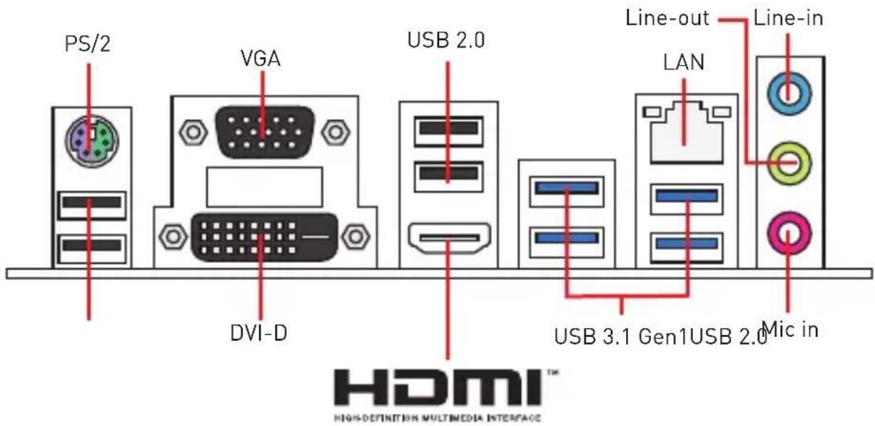
| Back Panel Connectors | 1x PS/2 keyboard/ mouse combo port4x USB 2.0 Type-A ports1x VGA port1x DVI-D port1x HDMITM port4x USB 3.1 Gen1 Type-A ports1x LAN (RJ45) port3x audio jacks |
| Internal Connectors | 1x 24-pin ATX main power connector1x 8-pin ATX 12V power connector4x SATA 6Gb/s connectors2x USB 2.0 connectors (supports additional 4 USB 2.0 ports1x USB 3.1 Gen1 connector (supports additional 2 USB 3.1 Gen1 ports) |
Continued on next page
Continued from previous page
| Internal Connectors | 1x 4-pin CPU fan connector2x 4-pin system fan connectors1x Front panel audio connector2x Front panel connectors1x TPM module connector1x Chassis Intrusion connector1x Serial port connector1x Parallel port connector1x RGB LED strip connector1x Clear CMOS jumper |
| Software | DriversAPP MANAGERSUPER CHARGERCOMMAND CENTERLIVE UPDATE 6MYSTIC LIGHTSMART TOOLX-BOOSTRAMDISKNorth SecurityGoogle Chrom Google Toolbar, Google DriveCPU-Z MSI GAMING |
Package contents
Please check the contents of your motherboard package. It should contain:
- Motherboard
- Driver DVD
- Quick Installation Guide
- I/O Shielding
- SATA 6G Cable x2
- Case Badge
• Product registration card
M.2 Screw x1

Important
If any of the above items are damaged or missing, please contact your retailer.
Rear I/O Panel
LAN Port LED Status Table
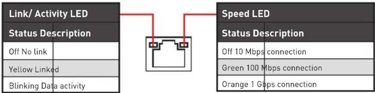
flowchart
graph LR
    A["Link/ Activity LED"] --> B["Speed LED"]
    C["Status Description"] --> A
    D["Off No link"] --> A
    E["Yellow Linked"] --> A
    F["Blinking Data activity"] --> A
    G["Off 10 Mbps connection"] --> A
    H["Green 100 Mbps connection"] --> A
    I["Orange 1 Gbps connection"] --> A
Audio 7.1-channel Configuration
To configure 7.1-channel audio, you have to connect front audio I/O module to JAUD1 connector and follow the below steps.
- Click on the Realtek HD Audio Manager > Advanced Settings to open the dialog below.
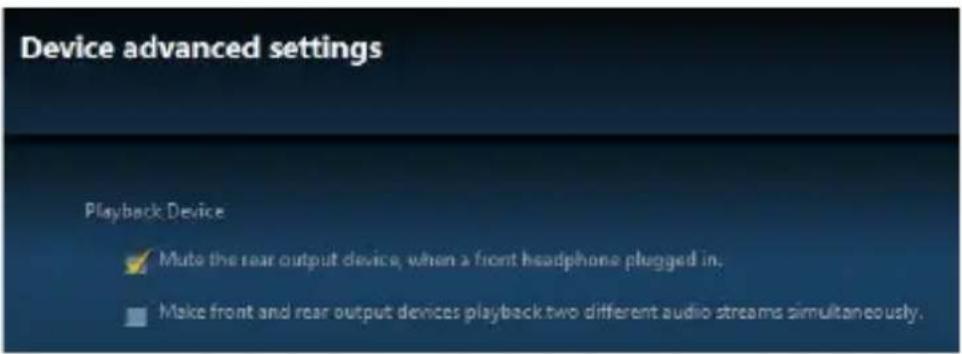
-
Select Mute the rear output device, when a front headphone plugged in.
-
Plug your speakers to audio jacks on rear and front I/O panel. When you plug into a device at an audio jack, a dialogue window will pop up asking you which device is current connected.
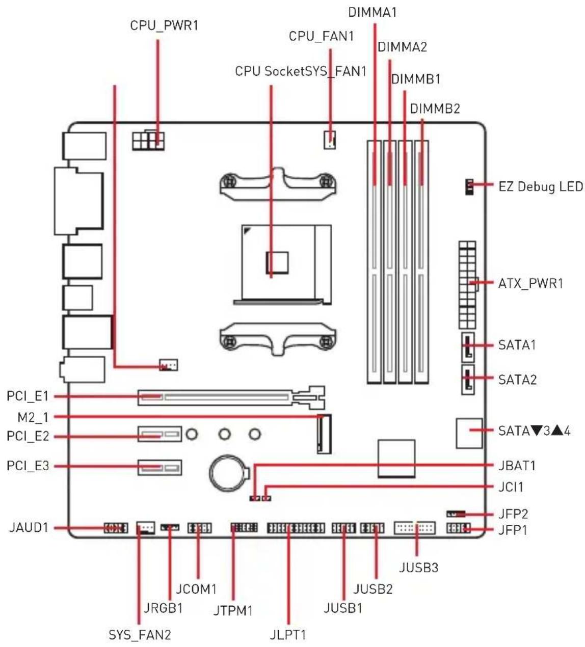
Overview of Components
CPU Socket
Please install the CPU into the CPU socket as shown below.
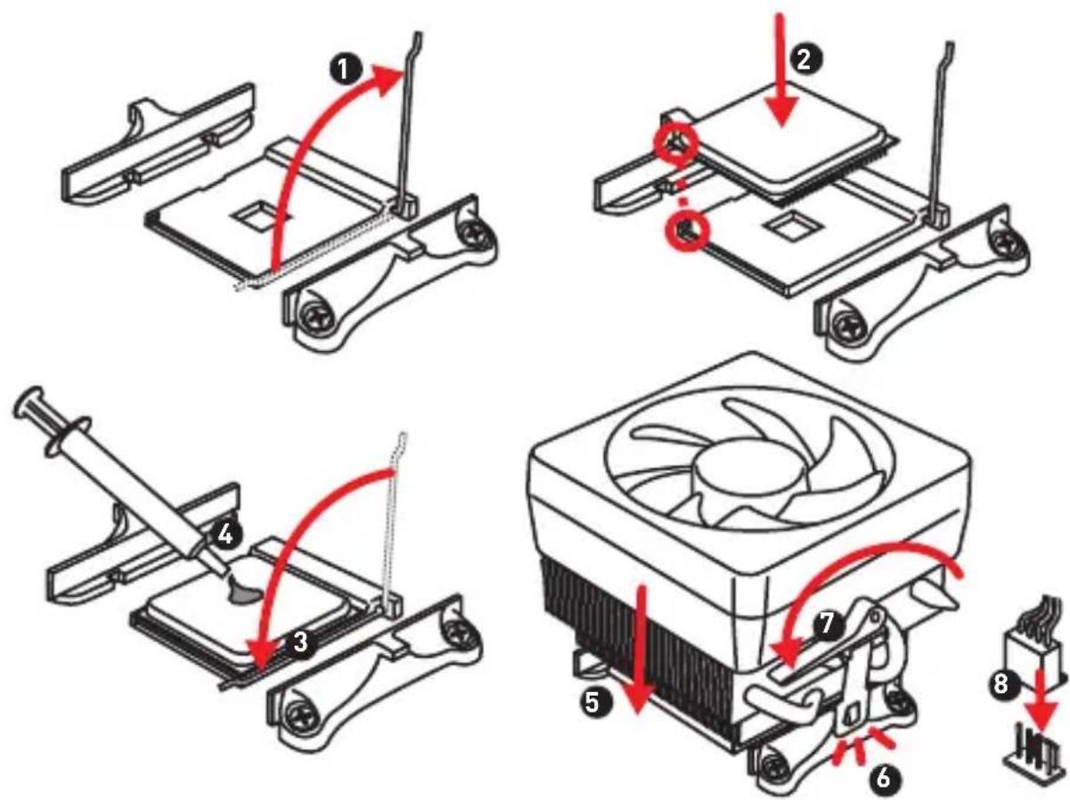

Important
When changing the processor, the system configuration could be cleared and reset BIOS to default values due to the AM4 processor's architecture.
Always unplug the power cord from the power outlet before installing or removing the CPU.
When installing a CPU, always remember to install a CPU heatsink. A CPU heatsink is necessary to prevent overheating and maintain system stability.
Confirm that the CPU heatsink has formed a tight seal with the CPU before booting your system.
Overheating can seriously damage the CPU and motherboard. Always make sure the cooling fans work properly to protect the CPU from overheating. Be sure to apply an even layer of thermal paste (or thermal tape) between the CPU and the heatsink to enhance heat dissipation.
If you purchased a separate CPU and heatsink/ cooler, Please refer to the documentation in the heatsink/ cooler package for more details about installation.
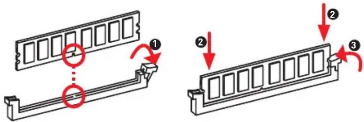
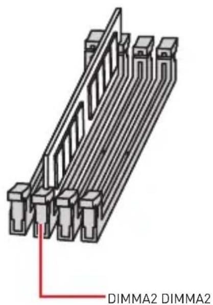
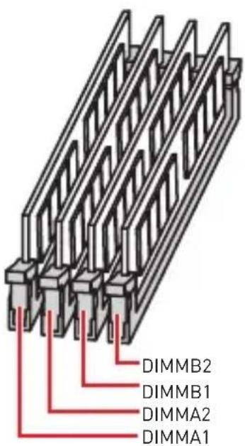
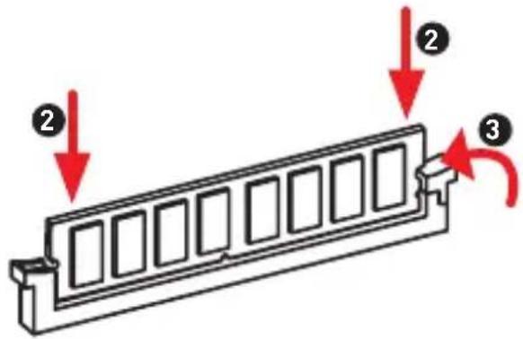
DIMM Slots
Please install the memory module into the DIMM slot as shown below.
Memory module installation recommendation
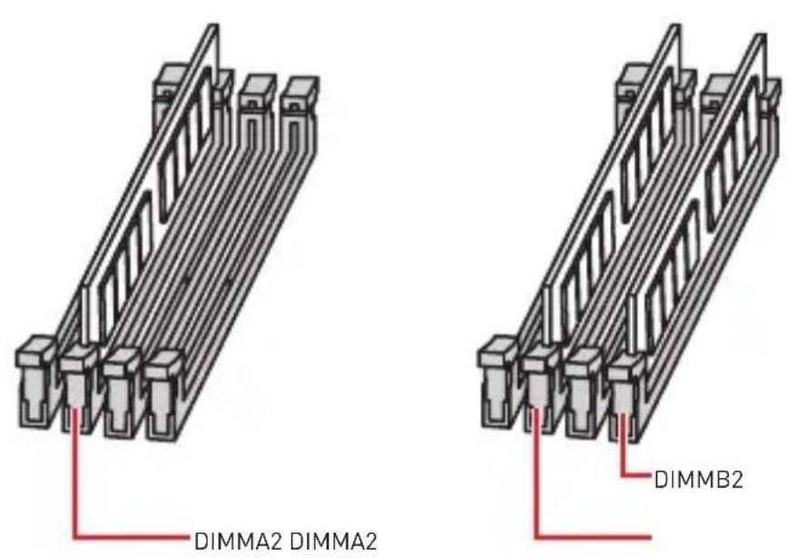
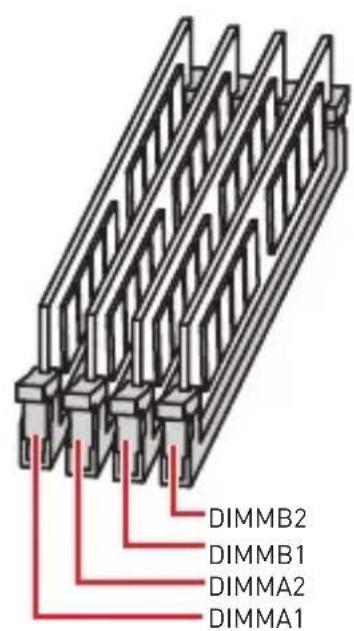

Important
Always insert memory modules in the DIMMA2 slot first.
Due to chipset resource usage, the available capacity of memory will be a little less than the amount of installed.
Based on processor specification, the Memory DIMM voltage below 1.35V is suggested to protect the processor.
Due to AM4 CPU/memory controller official specification limitation, the frequency of memory modules may operate lower than the marked value under the default state. Please refer www.msi.com for more information on compatible memory.
PCI\_E1\~3: PCIe Expansion Slots
| Slots\Processors | RyzenTM 1st and 2nd Generation | RyzenTM with RadeonTM Vega Graphics | AthlonTM with RadeonTM Vega Graphics |
| PCI_E1 PCIe 3.0 x16 | PCIe 3.0 x8 PCIe 3.0 x4 | ||
| PCI_E2 PCIe 2.0 x1 P | Cle 2.0 x1 PCIe 2.0 x1 | ||
| PCI_E3 PCIe 2.0 x1 P | Cle 2.0 x1 PCIe 2.0 x1 |

Important
When adding or removing expansion cards, always turn off the power supply and unplug the power supply power cable from the power outlet. Read the expansion card's documentation to check for any necessary additional hardware or software changes.
If you install a large and heavy graphics card, you need to use a tool such as MSI Gaming Series Graphics Card Bolster to support its weight to prevent deformation of the slot.
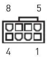
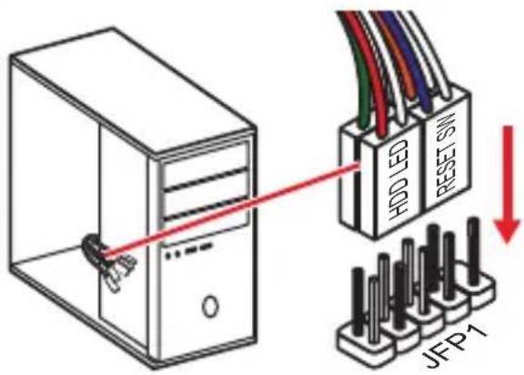
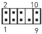
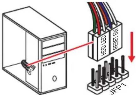
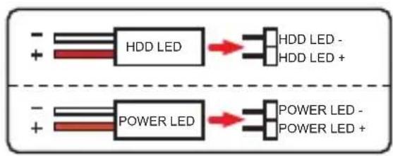
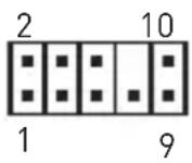
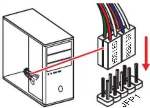
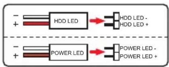
JFP1, JFP2: Front Panel Connectors
These connectors connect to the switches and LEDs on the front panel.
| Power LED Power Switch21+1+9ReservedHDD LED Reset Switch | 1 HDD LED + 2 Power LED + | ||
| 3 HDD LED - 4 Power LED - | |||
| 5 Reset Switch 6 Power Switch | |||
| 7 Reset Switch 8 Power Switch | |||
| 9 | Reserved | 10 No Pin | |

| JFP2 | 1 | Buzzer | 1 | Speaker - | 2 | Buzzer + |
| Speaker | 3 | Buzzer - | 4 | Speaker + |
SATA1\~4: SATA 6Gb/s Connectors
These connectors are SATA 6Gb/s interface ports. Each connector can connect to one SATA device.
Important
Please do not fold the SATA cable at a 90-degree angle. Data loss may result during transmission otherwise.
SATA cables have identical plugs on either sides of the cable. However, it is recommended that the flat connector be connected to the motherboard for space saving purposes.
M2\_1: M.2 Slot (Key M)
Please install the M.2 solid-state drive (SSD) into the M.2 slot as shown below.
ATX\_PWR1, CPU\_PWR1: Power Connectors
These connectors allow you to connect an ATX power supply.
1 | ATX_PWR1 | 1 +3.3V 13 +3.3V | ||
| 2 +3.3V 14 -12V | ||||
| 3 Ground 15 Ground | ||||
| 4 +5V 16 PS-ON# | ||||
| 5 Ground 17 Ground | ||||
| 6 +5V 18 Ground | ||||
| 7 Ground 19 Ground | ||||
| 8 PWR OK 20 Res | ||||
| 9 5 VSB 21 +5V | ||||
| 10 +12V 22 +5V | ||||
| 11 +12V 23 +5V | ||||
| 12 +3.3V 24 Ground |
 CPU_PWR1 CPU_PWR1 | 1 Ground 5 +12V | ||
| 2 Ground 6 +12V | |||
| 3 Ground 7 +12V | |||
| 4 Ground 8 +12V |
Important
Make sure that all the power cables are securely connected to a proper ATX power supply to ensure stable operation of the motherboard.
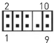
JUSB1\~2: USB 2.0 Connectors
These connectors allow you to connect USB 2.0 ports on the front panel.
 | 1 | VCC | 2 | VCC |
| 3 USB0- 4 USB1- | ||||
| 5 | USB0+ | 6 | USB1+ | |
| 7 Ground 8 Ground | ||||
| 9 | No Pin 10 | NC | ||

Important
- Note that the VCC and Ground pins must be connected correctly to avoid possible damage.
- In order to recharge your iPad,iPhone and iPod through USB ports, please install MSI® SUPER CHARGER utility.
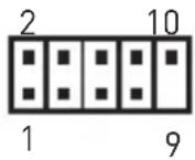
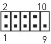
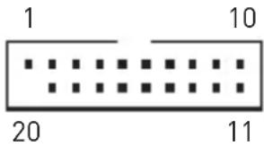
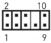
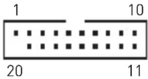
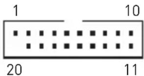
JUSB3: USB 3.1 Gen1 Connector
This connector allows you to connect USB 3.1 Gen1 ports on the front panel.
 | 1 Power 11 USB2.0+ | ||
| 2 USB3_RX_DN 12 USB2.0- | |||
| 3 USB3_RX_DP 13 Ground | |||
| 4 Ground 14 USB3_TX_C_DP | |||
| 5 USB3_TX_C_DN | 15 | USB3_TX_C_DN | |
| 6 USB3_TX_C_DP | 16 Ground | ||
| 7 Ground 17 USB3_RX_DP | |||
| 8 USB2.0- 18 | USB3_RX_DN | ||
| 9 USB2.0+ 19 | Power | ||
| 10 NC | 20 | No Pin |

Important
Note that the Power and Ground pins must be connected correctly to avoid possible damage.
CPU\_FAN1, SYS\_FAN1\~2: Fan Connectors
Fan connectors can be classified as PWM (Pulse Width Modulation) Mode or DC Mode. PWM Mode fan connectors provide constant 12V output and adjust fan speed with speed control signal. DC Mode fan connectors control fan speed by changing voltage. When you plug a 3-pin (Non-PWM) fan to a fan connector in PWM mode, the fan speed will always maintain at 100%, which might create a lot of noise. You can follow the instruction below to adjust the fan connector to PWM or DC Mode.
You can switch between PWM mode and DC mode and adjust fan speed in BIOS > HARDWARE MONITOR.
Select PWM mode or DC mode
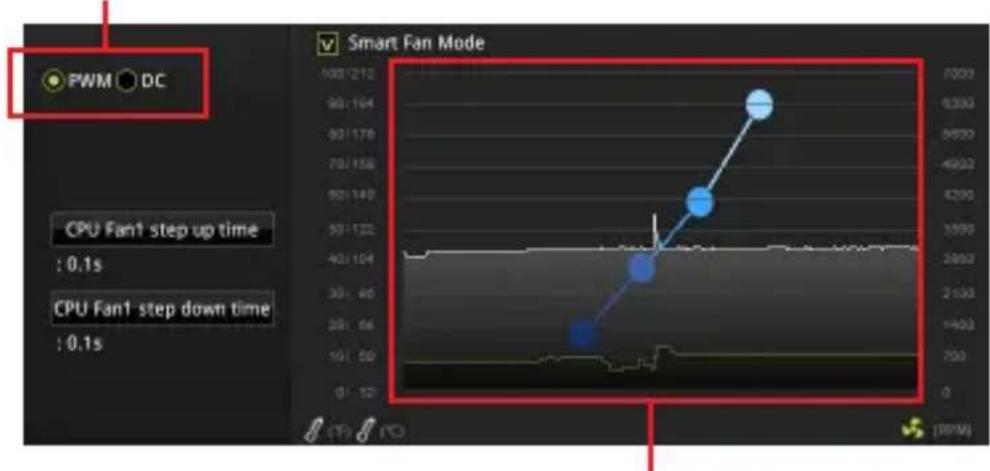
line
| Time | Smart Fan Mode | |------|----------------| | 0 | 20 | | 10 | 30 | | 20 | 40 | | 30 | 50 | | 40 | 60 | | 50 | 70 | | 60 | 80 | | 70 | 90 | | 80 | 100 | | 90 | 110 | | 100 | 120 |There are gradient points of the fan speed that allow you to adjust fan speed in relation to CPU temperature.

Important
Make sure fans are working properly after switching the PWM/ DC mode.
Pin definition of fan connectors
| PWM Mode pin definition | |||
| 1 | Ground 2 +1 | 2V | |
| 3 | Sense 4 Speed | ed Control | Signal |
| DC Mode pin definition | |||
| 1 G | Ground 2 Vol | ltage | Control |
| 3 S | Sense 4 NC | ||
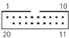
JTPM1: TPM Module Connector
This connector is for TPM (Trusted Platform Module). Please refer to the TPM security platform manual for more details and usages.
 | 1 LPC Clock 2 3V Standby power | ||
| 3 LPC Reset 4 3.3V Power | |||
| 5 LPC address & data pin0 6 Serial IRQ | |||
| 7 LPC address & data pin1 8 5V Power | |||
| 9 LPC address & data pin2 10 No Pin | |||
| 11 LPC address & data pin3 12 | Ground | ||
| 13 LPC Frame 14 | Ground | ||
JCI1: Chassis Intrusion Connector
This connector allows you to connect the chassis intrusion switch cable.

Normal (default)

Trigger the chassis intrusion event
Using chassis intrusion detector
- Connect the JCI1 connector to the chassis intrusion switch/ sensor on the chassis.
- Close the chassis cover.
- Go to BIOS > SETTINGS > Security > Chassis Intrusion Configuration.
- Set Chassis Intrusion to Enabled.
- Press F10 to save and exit and then press the Enter key to select Yes.
- Once the chassis cover is opened again, a warning message will be displayed on screen when the computer is turned on.
Resetting the chassis intrusion warning
- Go to BIOS > SETTINGS > Security > Chassis Intrusion Configuration.
- Set Chassis Intrusion to Reset.
- Press F10 to save and exit and then press the Enter key to select Yes.
JAUD1: Front Audio Connector
This connector allows you to connect audio jacks on the front panel.
 | 1 MIC L 2 Ground | ||
| 3 MIC R 4 NC | |||
| 5 Head Phone R 6 MIC Detection | |||
| 7 SENSE_SEND 8 No Pin | |||
| 9 Head Phone L 10 Head Phone Detection |
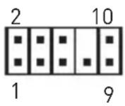
JCOM1: Serial Port Connector
This connector allows you to connect the optional serial port with bracket.
 | 1 DCD 2 SIN | |||
| 3 SOUT 4 DTR | ||||
| 5 Ground 6 DSR | ||||
| 7 | RTS | 8 CTS | ||
| 9 RI | 10 No Pin | |||
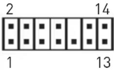
JLPT1: Parallel Port Connector
This connector allows you to connect the optional parallel port with bracket.
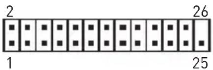 | |||||
| 1 | RSTB# | 2 | AFD# | 3 | PRND0 |
| 4 | ERR# | 5 | PRND1 | 6 | PINIT# |
| 7 | PRND2 | 8 | LPT_SLIN# | 9 | PRND3 |
| 10 | Ground | 11 | PRND4 | 12 | Ground |
| 13 | PRND5 | 14 | Ground | 15 | PRND6 |
| 16 | Ground | 17 | PRND7 | 18 | Ground |
| 19 | ACK# | 20 | Ground | 21 | BUSY |
| 22 | Ground | 23 PE 24 Ground | |||
| 25 | SLCT | 26 No Pin | |||
JBAT1: Clear CMOS (Reset BIOS) Jumper
There is CMOS memory onboard that is external powered from a battery located on the motherboard to save system configuration data. If you want to clear the system configuration, set the jumpers to clear the CMOS memory.

Keep Data (default)

Clear CMOS/ Reset BIOS
Resetting BIOS to default values
- Power off the computer and unplug the power cord.
- Use a jumper cap to short JBAT1 for about 5-10 seconds.
- Remove the jumper cap from JBAT1.
- Plug the power cord and power on the computer.
EZ Debug LED: Debug LED indicators
These LEDs indicate the status of the motherboard.
□ CPU - indicates CPU is not detected or fail.
☐ DRAM - indicates DRAM is not detected or fail.
☐ VGA - indicates GPU is not detected or fail.
☐BOOT - indicates booting device is not detected or fail.
JRGB1: RGB LED strip connector
This connector allows you to connect the 5050 RGB LED strip.
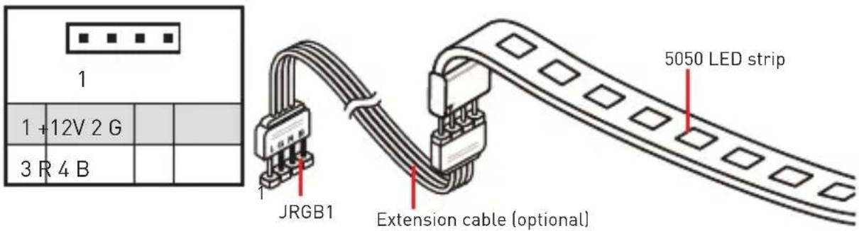
Important
This connector supports 5050 RGB multi-color LED strips (12V/G/R/B) with the maximum power rating of 3A (12V). Please keeping the LED strip shorter than 2 meters to prevent dimming.
Always turn off the power supply and unplug the power cord from the power outlet before installing or removing the RGB LED strip.
Please use MSI's software to control the extended LED strip.
BIOS Setup
The default settings offer the optimal performance for system stability in normal conditions. You should always keep the default settings to avoid possible system damage or failure booting unless you are familiar with BIOS.

Important
BIOS items are continuous update for better system performance. Therefore, the description may be slightly different from the latest BIOS and should be held for reference only. You could also refer to the HELP information panel for BIOS item description.
The pictures in this chapter are for reference only and may vary from the product you purchased.
The BIOS items will vary with the processor.
Entering BIOS Setup
Press Delete key, when the Press DEL key to enter Setup Menu, F11 to enter Boot Menu message appears on the screen during the boot process.
Function key
F1: General Help
F2: Add/ Remove a favorite item
F3: Enter Favorites menu
F4: Enter CPU Specifications menu
F5: Enter Memory-Z menu
F6: Load optimized defaults
F7: Switch between Advanced mode and EZ mode
F8: Load Overclocking Profile
F9: Save Overclocking Profile
F10: Save Change and Reset*
F12: Take a screenshot and save it to USB flash drive (FAT/ FAT32 format only).
* When you press F10, a confirmation window appears and it provides the modification information. Select between Yes or No to confirm your choice.
Resetting BIOS
You might need to restore the default BIOS setting to solve certain problems. There are several ways to reset BIOS:
- Go to BIOS and press F6 to load optimized defaults.
- Short the Clear CMOS jumper on the motherboard.

Important
Please refer to the Clear CMOS jumper section for resetting BIOS.
Updating BIOS
Updating BIOS with M-FLASH
Before updating:
Please download the latest BIOS file that matches your motherboard model from MSI website. And then save the BIOS file into the USB flash drive.
Updating BIOS:
- Press Del key to enter the BIOS Setup during POST.
- Insert the USB flash drive that contains the update file into the computer.
- Select the M-FLASH tab and click on Yes to reboot the system and enter the flash mode.
- Select a BIOS file to perform the BIOS update process.
- After the flashing process is 100% completed, the system will reboot automatically.
Updating the BIOS with Live Update 6
Before updating:
Make sure the LAN driver is already installed and the Internet connection is set properly.
Updating BIOS:
- Install and launch MSI LIVE UPDATE 6.
- Select BIOS Update.
- Click on Scan button.
- Click on Download icon to download and install the latest BIOS file.
- Click Next and choose In Windows mode. And then click Next and Start to start updating BIOS.
- After the flashing process is 100% completed, the system will restart automatically.
Software Description
Please download and update the latest utilities and drivers at www.msi.com
Installing Windows® 10
- Power on the computer.
- Insert the Windows ^® 10 disc into your optical drive.
- Press the Restart button on the computer case.
- Press F11 key during the computer POST (Power-On Self Test) to get into Boot Menu.
- Select your optical drive from the Boot Menu.
- Press any key when screen shows Press any key to boot from CD or DVD... message.
- Follow the instructions on the screen to install Windows ^® 10.
Installing Drivers
- Start up your computer in Windows ^® 10.
- Insert MSI® Driver Disc into your optical drive.
- The installer will automatically appear and it will find and list all necessary drivers.
- Click Install button.
- The software installation will then be in progress, after it has finished it will prompt you to restart.
- Click OK button to finish.
- Restart your computer.
Installing Utilities
Before you install utilities, you must complete drivers installation.
- Insert MSI® Driver Disc into your optical drive.
- The installer will automatically appear.
- Click Utilities tab.
- Select the utilities you want to install.
- Click Install button.
- The utilities installation will then be in progress, after it has finished it will prompt you to restart.
- Click OK button to finish.
- Restart your computer.
JUSB3: USB 3.1 Gen1 커넥터....13
CPU_FAN1, SYS_FAN1\~2: 팬 커넥터 14
LAN 포트 LED 상태 표시도
flowchart
graph LR
    A["링크/ 통신 LED"] --> B[" LN 1 LAN이 올바르게 연결되지 않았습니다. "]
    C["속도 LED"] --> D[" LN 2 LAN이 올바르게 연결되었습니다. "]
    E["꺼짐"] --> F[" LAN 3 LAN이 올바르게 연결되었습니다. "]
    G["노란색"] --> H[" LAN 4 LAN이 올바르게 연결되었습니다. "]
    I[" Nak박임"] --> J[" LAN 5 컴퓨터가 LAN으로 정상적인 통신중입니다. "]
    K[" ---------- "] --> L[" ---------- |<br>    L --> M[ ---------- |<br>    M --> N[ ---------- |<br>    N --> O[ ---------- |<br>    O --> P[ ---------- |<br>    P --> Q[ ---------- |<br>    Q --> R[ ---------- |<br>    R --> S[ ---------- |<br>    S --> T[ ---------- |<br>    T --> U[ ---------- |<br>    U --> V[ ---------- |<br>    V --> W[ ---------- |<br>    W --> X[ ---------- |<br>    X --> Y[ ---------- |<br>    Y --> Z[ ---------- |<br>    Z --> AA[ ---------- |<br>    AA --> AB[ ---------- |<br>    AB --> AC[ ---------- |<br>    AC --> AD[ ---------- |<br>    AD --> AE[ ---------- |<br>    AE --> AF[ ---------- |<br>    AF --> AG[ ---------- |<br>    AG --> AH[ ---------- |<br>    AH --> AI[ ---------- |<br>    AI --> AJ[ ---------- |<br>    AJ --> AK[ ---------- |<br>    AK --> AL[ ---------- |<br>    AL --> AM[ ---------- |<br>    AM --> AN[ ---------- |<br>    AN --> AO[ ---------- |<br>    AO --> AP[ ---------- |<br>    AP --> AQ[ ---------- |<br>    AQ --> AR[ ---------- |<br>    AR --> AS[ ---------- |<br>    AS --> AT[ ---------- |<br>    AT --> AU[ ---------- |<br>    AU --> AV[ ---------- |<br>    AV --> AW[ ---------- |<br>    AW --> AX[ ---------- |<br>    AX --> AY[ ---------- |<br>    AY --> AZ[ ---------- |<br>    AZ --> BA[ ---------- |<br>    BA --> BB[ ---------- |<br>    BB --> BC[ ---------- |<br>    BC --> BD[ ---------- |<br>    BD --> BE[ ---------- |<br>    BE --> BF[ ---------- |<br>    BF --> BG[ ---------- |<br>    BG --> BH[ ---------- |<br>    BH --> BI[ ---------- |<br>    BI --> BJ[ ---------- |<br>    BJ --> BK[ ---------- |<br>    BK --> BL[ ---------- |<br>    BL --> BM[ ---------- |<br>    BM --> BN[ ---------- |<br>    BN --> BO[ ---------- |<br>    BO --> BP[ ---------- |<br>    BP --> BQ[ ---------- |<br>    BQ --> BR[ ---------- |<br>    BR --> BS[ ---------- |<br>    BS --> BT[ ---------- |<br>    BT --> BU[ ---------- |<br>    BU --> BV[ ---------- |<br>    BV --> BW[ ---------- |<br>    BW --> BX[ ---------- |<br>    BX --> BY[ ---------- |<br>    BY --> BZ[ ---------- |<br>    BZ --> CA[ ---------- |<br>    CA --> CB[ ---------- |<br>    CB --> CC[ ----------"]
    CC --> CD[" ----------"]
    CD --> CE[" ----------"]
오디오 7.1-채널 구성 도표
⚠️ 중요사항

메모리 모듈 설치(추천)

natural_image
3D technical illustration of a mechanical component with zigzag grooves and connectors, labeled DIMMA2 (no text or symbols on the diagram itself)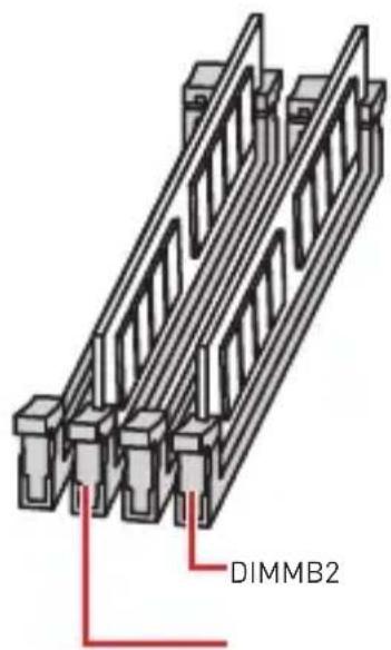


중요사항
| Power LED Power SwitchJFP1 2 1 9ReservedHDD LED Reset Switch | 1 HDD LED + 2 Power _LED + | ||
| 3 HDD LED - 4 Power LED - | |||
| 5 Reset Switch 6 Power Switch | |||
| 7 Reset Switch 8 Power Switch | |||
| 9 | Reserved | 10 No Pin | |

| JFP2 | 1 | Speaker - | 2 | Buzzer + |
| 3 | Buzzer - | 4 | Speaker + |
SATA1\~4: SATA 6Gb/s 커넥터
| 1 Power 11 USB2.0+ | ||
| 2 USB3_RX_DN 12 USB2.0- | |||
| 3 USB3_RX_DP 13 Ground | |||
| 4 Ground 14 USB3_TX_C_DP | |||
| 5 USB3_TX_C_DN | 15 | USB3_TX_C_DN | |
| 6 USB3_TX_C_DP | 16 Ground | ||
| 7 Ground 17 USB3_RX_DP | |||
| 8 USB2.0- 18 | USB3_RX_DN | ||
| 9 USB2.0+ 19 | Power | ||
| 10 NC | 20 | No Pin |

중요사항
 | 1 MIC L 2 Ground | ||
| 3 MIC R 4 NC | |||
| 5 Head Phone R 6 MIC Detection | |||
| 7 SENSE_SEND 8 No Pin | |||
| 9 Head Phone L 10 Head Phone Detection |
JCOM1: 시리얼 포트 커넥터

Important


Important
| Power LED Power SwitchJFP1 2 1 + + + 9Reserved HDD LED Reset Switch | 1 HDD LED + 2 Power LED + | ||
| 3 HDD LED - 4 Power LED - | |||
| 5 Reset Switch 6 | Power Switch | ||
| 7 Reset Switch 8 | Power Switch | ||
| 9 | Reserved | 10 No Pin | |
| JFP2 | 1 | Buzzer | 1 | Speaker - | 2 | Buzzer + |
| Speaker | 3 | Buzzer - | 4 | Speaker + |
| 1 Power 11 USB2.0+ | ||
| 2 USB3_RX_DN 12 USB2.0- | |||
| 3 USB3_RX_DP 13 Ground | |||
| 4 Ground 14 USB3_TX_C_DP | |||
| 5 USB3_TX_C_DN | 15 | USB3_TX_C_DN | |
| 6 USB3_TX_C_DP | 16 Ground | ||
| 7 Ground 17 USB3_RX_DP | |||
| 8 USB2.0- 18 | USB3_RX_DN | ||
| 9 USB2.0+ 19 | Power | ||
| 10 NC | 20 | No Pin |

Important
| 1 MIC L 2 Ground | ||
| 3 MIC R 4 NC | |||
| 5 Head Phone R 6 MIC Detection | |||
| 7 SENSE_SEND 8 No Pin | |||
| 9 Head Phone L 10 Head Phone Detection |
JFP1, JFP2: Frontpanel-Anschlüsse....11
SATA1\~4: SATA 6Gb/s Anschlüsse ....11
JUSB1\~2: USB 2.0 Anschlüsse....13
JUSB3: USB 3.1 Gen1 Anschluss....13
Installation von Utilities....20
Sicherheitshinweis

Wichtig
natural_image
3D technical illustration of a mechanical component with zigzag grooves and connectors, labeled DIMMA2 (no text or symbols on the diagram itself)


Wichtig
JFP1, JFP2: Frontpanel-Anschlüsse
| Power LED Power SwitchJFP1 2 1 + + + 9Reserved HDD LED Reset Switch | 1 HDD LED + 2 Power LED + | ||
| 3 HDD LED - 4 Power LED - | |||
| 5 Reset Switch 6 Power Switch | |||
| 7 Reset Switch 8 Power Switch | |||
| 9 Reserved | 10 | No Pin | |


| JFP2 | 1 | Buzzer | 1 | Speaker - | 2 | Buzzer + |
| Speaker | 3 | Buzzer - | 4 | Speaker + |
SATA1\~4: SATA 6Gb/s Anschlüsse
ATX\_PWR1, CPU\_PWR1: Stromanschlüsse
JUSB1\~2: USB 2.0 Anschlüsse
 | 1 Power 11 USB2.0+ | ||
| 2 USB3_RX_DN 12 USB2.0- | |||
| 3 USB3_RX_DP 13 Ground | |||
| 4 Ground 14 USB3_TX_C_DP | |||
| 5 USB3_TX_C_DN | 15 | USB3_TX_C_DN | |
| 6 USB3_TX_C_DP | 16 Ground | ||
| 7 Ground 17 USB3_RX_DP | |||
| 8 USB2.0- 18 | USB3_RX_DN | ||
| 9 USB2.0+ 19 | Power | ||
| 10 NC | 20 | No Pin |

Wichtig
 | 1 MIC L 2 Ground | ||
| 3 MIC R 4 NC | |||
| 5 Head Phone R 6 MIC Detection | |||
| 7 SENSE_SEND 8 No Pin | |||
| 9 Head Phone L 10 Head Phone Detection |

Внимание!
natural_image
3D technical illustration of a mechanical component with zigzag grooves and connectors, labeled DIMMA2 (no text or symbols on the diagram itself)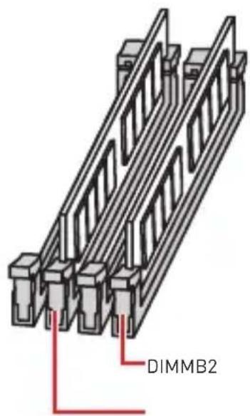


Внимание!
| Power LED Power SwitchJFP1 2 1 9ReservedHDD LED Reset Switch | 1 HDD LED + 2 Power LED + | ||
| 3 HDD LED - 4 Power LED - | |||
| 5 Reset Switch 6 | Power Switch | ||
| 7 Reset Switch 8 | Power Switch | ||
| 9 | Reserved | 10 No Pin | |
| JFP2 | 1 | Speaker - | 2 | Buzzer + |
| 3 | Buzzer - | 4 | Speaker + |
 | 1 Power 11 USB2.0+ | ||
| 2 USB3_RX_DN 12 USB2.0- | |||
| 3 USB3_RX_DP 13 Ground | |||
| 4 Ground 14 USB3_TX_C_DP | |||
| 5 USB3_TX_C_DN 15 | USB3_TX_C_DN | ||
| 6 USB3_TX_C_DP | 16 Ground | ||
| 7 Ground 17 USB3_RX_DP | |||
| 8 USB2.0- 18 | USB3_RX_DN | ||
| 9 USB2.0+ 19 | Power | ||
| 10 NC | 20 | No Pin | |

Внимание!
 | 1 MIC L 2 Ground | ||
| 3 MIC R 4 NC | |||
| 5 Head Phone R 6 MIC Detection | |||
| 7 SENSE_SEND 8 No Pin | |||
| 9 Head Phone L 10 Head Phone Detection |
注意

内存模块安装建议
natural_image
3D technical illustration of a mechanical component with zigzag grooves and connectors, labeled DIMMA2 (no text or symbols on the diagram itself)

注意
| Power LED Power SwitchJFP1 2 1 9Reserved HDD LED Reset Switch | 1 HDD LED + 2 Power _LED + | ||
| 3 HDD LED - 4 Power LED - | |||
| 5 Reset Switch 6 | Power Switch | ||
| 7 Reset Switch 8 | Power Switch | ||
| 9 | Reserved | 10 No Pin | |


flowchart
graph LR
    A["+ HDD LED"] --> B["HD- HDD LED +"]
    C["+ POWER LED"] --> D["HD- POWER LED +"]
    style A fill:#f9f,stroke:#333
    style C fill:#f9f,stroke:#333
| JFP2 | 1 | Buzzer | 1 | Speaker - | 2 | Buzzer + |
| Speaker | 3 | Buzzer - | 4 | Speaker + |
SATA1\~4: SATA 6Gb/s 接口
ATX\_PWR1, CPU\_PWR1: 电源接口
 | 1 Power 11 USB2.0+ | |||
| 2 USB3_RX_DN 12 USB2.0- | ||||
| 3 USB3_RX_DP 13 Ground | ||||
| 4 Ground 14 USB3_TX_C_DP | ||||
| 5 | USB3_TX_C_DN | 15 | USB3_TX_C_DN | |
| 6 | USB3_TX_C_DP | 16 Ground | ||
| 7 Ground 17 | USB3_RX_DP | |||
| 8 USB2.0- | 18 | USB3_RX_DN | ||
| 9 USB2.0+ | 19 | Power | ||
| 10 | NC | 20 | No Pin | |

注意
| 1 MIC L 2 Ground | ||
| 3 MIC R 4 NC | |||
| 5 Head Phone R 6 MIC Detection | |||
| 7 SENSE_SEND 8 No Pin | |||
| 9 Head Phone L 10 Head Phone Detection |
JCOM1: 串行端头接口
此接口允许您连接可选串行端口可用插槽。
| 1 DCD 2 SIN | ||
| 3 SOUT 4 DTR | |||
| 5 | Ground | 6 D$R | |
| 7 | RTS | 8 CTS | |
| 9 RI | 10 No Pin |
JLPT1: 并行端头接口
此接口允许您连接可选并行端口可用插槽。
| |||||
| 1 | RSTB# | 2 | AFD# | 3 | PRND0 |
| 4 | ERR# | 5 | PRND1 | 6 | PINIT# |
| 7 | PRND2 | 8 | LPT_SLIN# | 9 | PRND3 |
| 10 | Ground | 11 | PRND4 | 12 | Ground |
| 13 | PRND5 | 14 | Ground | 15 | PRND6 |
| 16 | Ground | 17 | PRND7 | 18 | Ground |
| 19 | ACK# | 20 | Ground | 21 | BUSY |
| 22 | Ground | 23 PE 24 Ground | |||
| 25 | SLCT | 26 | No Pin | ||
JBAT1: 清除 CMOS (重启 BIOS) 跳线
重要
記憶體模組安裝建議

natural_image
3D technical illustration of a mechanical component with zigzag grooves and connectors, labeled DIMMA2 (no text or symbols on the diagram itself)


重要
| Power LED Power SwitchJFP1 2 1 9Reserved HDD LED Reset Switch | 1 HDD LED + 2 Power _LED + | ||
| 3 HDD LED - 4 | Power LED - | ||
| 5 Reset Switch 6 | Power Switch | ||
| 7 Reset Switch 8 | Power Switch | ||
| 9 | Reserved | 10 No Pin | |


flowchart
graph LR
    A["+ HDD LED"] --> B["HD- HDD LED +"]
    C["+ POWER LED"] --> D["HD- POWER LED +"]
    style A fill:#f9f,stroke:#333
    style C fill:#f9f,stroke:#333
| JFP2 | 1 | Speaker - | 2 | Buzzer + |
| 3 | Buzzer - | 4 | Speaker + |
SATA1\~4: SATA 6Gb/s 插孔
 | 1 Power 11 USB2.0+ | ||
| 2 USB3_RX_DN 12 USB2.0- | |||
| 3 USB3_RX_DP 13 Ground | |||
| 4 Ground 14 USB3_TX_C_DP | |||
| 5 USB3_TX_C_DN | 15 | USB3_TX_C_DN | |
| 6 USB3_TX_C_DP | 16 Ground | ||
| 7 Ground 17 USB3_RX_DP | |||
| 8 USB2.0- 18 | USB3_RX_DN | ||
| 9 USB2.0+ 19 | Power | ||
| 10 NC | 20 | No Pin |

重要
| 1 MIC L 2 Ground | ||
| 3 MIC R 4 NC | |||
| 5 Head Phone R 6 MIC Detection | |||
| 7 SENSE_SEND 8 No Pin | |||
| 9 Head Phone L 10 Head Phone Detection |
JCOM1: 序列埠接頭
此接頭用來連接選擇性配置的序列埠托架。
| 1 DCD 2 SIN | ||
| 3 SOUT 4 DTR | |||
| 5 | Ground | 6 D$R | |
| 7 | RTS | 8 CTS | |
| 9 RI | 10 No Pin |
JLPT1: 平行埠接頭
此接頭用來連接選擇性配置的平行埠托架。
| |||||
| 1 | RSTB# | 2 | AFD# | 3 | PRND0 |
| 4 | ERR# | 5 | PRND1 | 6 | PINIT# |
| 7 | PRND2 | 8 | LPT_SLIN# | 9 | PRND3 |
| 10 | Ground | 11 | PRND4 | 12 | Ground |
| 13 | PRND5 | 14 | Ground | 15 | PRND6 |
| 16 | Ground | 17 | PRND7 | 18 | Ground |
| 19 | ACK# | 20 | Ground | 21 | BUSY |
| 22 | Ground | 23 PE 24 Ground | |||
| 25 | SLCT | 26 No Pin | |||
注意

メモリモジュールの推薦取付順序

natural_image
3D technical illustration of a mechanical component with zigzag grooves and connectors, labeled DIMMA2 (no text or symbols on the diagram itself)


注意
| Power LED Power SwitchJFP1 2 1 9Reserved HDD LED Reset Switch | 1 HDD LED + 2 | Power LED + |
| 3 | 4 | |
| 5 | 6 | |
| 7 | 8 | |
| 9 | 10 |


| JFP2 | 1 | Buzzer | 1 | Speaker - | 2 | Buzzer + |
| Speaker | 3 | Buzzer - | 4 | Speaker + |
 | 1 Power 11 USB2.0+ | |||
| 2 USB3_RX_DN 12 USB2.0- | ||||
| 3 | USB3_RX_DP | 13 | Ground | |
| 4 Ground 14 | USB3_TX_C_DP | |||
| 5 | USB3_TX_C_DN | 15 | USB3_TX_C_DN | |
| 6 | USB3_TX_C_DP | 16 | Ground | |
| 7 Ground 17 | USB3_RX_DP | |||
| 8 | USB2.0- | 18 | USB3_RX_DN | |
| 9 | USB2.0+ | 19 | Power | |
| 10 | NC | 20 | No Pin | |

注意
 | 1 MIC L 2 Ground | ||
| 3 MIC R 4 NC | |||
| 5 Head Phone R 6 MIC Detection | |||
| 7 SENSE_SEND 8 No Pin | |||
| 9 Head Phone L 10 Head Phone Detection |
JCOM1: シリアルポートコネクター
FCC Compliance Statement
Note: This equipment has been tested and found to comply with the limits for a Class B digital device, pursuant to part 15 of the FCC Rules. These limits are designed to provide reasonable protection against harmful interference in a residential installation. This equipment generates, uses and can radiate radio frequency energy and, if not installed and used in accordance with the instructions, may cause harmful interference to radio communications. However, there is no guarantee that interference will not occur in a particular installation. If this equipment does cause harmful interference to radio or television reception, which can be determined by turning the equipment off and on, the user is encouraged to try to correct the interference by one or more of the following measures:
• Reorient or relocate the receiving antenna.
- Increase the separation between the equipment and receiver.
- Connect the equipment into an outlet on a circuit different from that to which the receiver is connected.
- Consult the dealer or an experienced radio/TV technician for help.
Caution: Changes or modifications not expressly approved by the party responsible for compliance could void the user's authority to operate the equipment.

Tested to comply with FCC standards FOR HOME OR OFFICE USE
This device complies with part 15 of the FCC Rules. Operation is subject to the following two conditions:
(1) This device may not cause harmful interference, and (2) this device must accept any interference received, including interference that may cause undesired operation.
CE Conformity

Products bearing the CE marking comply with one or more of the following EU Directives as may be applicable:
RED 2014/53/EU; Low Voltage Directive 2014/35/EU; EMC Directive 2014/30/EU; RoHS Directive 2011/65/EU.
Compliance with these directives is assessed using applicable European Harmonized Standards. The point of contact for regulatory matters is MSI, MSI-NL Eindhoven 5706 5692 ER Son.
C-Tick Compliance

N1996
B급 기기(가정용 방송통신기자재)

Batteries, battery packs, and accumulators should not be disposed of as unsorted household waste. Please use the public collection system to return, recycle, or treat them in compliance with the local regulations.
Taiwan:

廢電池請回收
For better environmental protection, waste batteries should be collected separately for recycling or special disposal.
California, USA:

The button cell battery may contain perchlorate material and requires special handling when recycled or disposed of in California. For further information please visit:
http://www.dtsc.ca.gov/hazardouswaste/perchlorate/
CAUTION: There is a risk of explosion, if battery is incorrectly replaced.
Replace only with the same or equivalent type recommended by the manufacturer.
Chemical Substances Information
In compliance with chemical substances regulations, such as the EU REACH Regulation (Regulation EC No. 1907/2006 of the European Parliament and the Council), MSI provides the information of chemical substances in products at:
http://www.msi.com/html/popup/csr/evmtprtt_pcm.html
WEEE (Waste Electrical and Electronic Equipment) Statement
ENGLISH
To protect the global environment and as an environmentalist, MSI must remind you that...
Under the European Union ("EU") Directive on Waste Electrical and Electronic Equipment, Directive 2002/96/EC, which takes effect on August 13, 2005, products of “electrical and electronic equipment” cannot be discarded as municipal wastes anymore, and manufacturers of covered electronic equipment will be obligated to take back such products at the end of their useful life. MSI will comply with the product take back requirements at the end of life of MSI-branded products that are sold into the EU. You can return these products to local collection points.

DEUTSCH
This product complies with the “India E-waste (Management and Handling) Rule 2011” and prohibits use of lead, mercury, hexavalent chromium, polybrominated biphenyls or polybrominated diphenyl ethers in concentrations exceeding 0.1 weight % and 0.01 weight % for cadmium, except for the exemptions set in Schedule 2 of the Rule.
Environmental Policy
- The product has been designed to enable proper reuse of parts and recycling and should not be thrown away at its end of life.
- Users should contact the loca authorized point of collection
for recycling and disposing of their end-of-life products.
- Visit the MSI website and locate a nearby distributor for further recycling information.
Users may also reach us at gpcontdev@msi.com for information regarding proper Disposal, Take-back, Recycling, and Disassembly of MSI products.

产品中有害物质的名称及含量
Copyright © 2018 All rights reserved.
The MSI logo used is a registered trademark of Micro-Star Int'l Co., Ltd. All other marks and names mentioned may be trademarks of their respective owners. No warranty as to accuracy or completeness is expressed or implied. MSI reserves the right to make changes to this document without prior notice.
Technical Support
If a problem arises with your system and no solution can be obtained from the user guide, please contact your place of purchase or local distributor. Alternatively, please try the following help resources for further guidance.
- Visit the MSI website for technical guide, BIOS updates, driver updates, and other information: http://www.msi.com
- Register your product at: http://register.msi.com
Revision History
Version 6.0, 2018/10, first release.
- Contents
- Safety Information....2
- Specifications....3
- Package contents 5
- Rear I/O Panel 6
- Overview of Components 7
- BIOS Setup 18
- Software Description....20
- Safety Information
- Specifications
- Package contents
- Important
- Rear I/O Panel
- LAN Port LED Status Table
- Audio 7.1-channel Configuration
- Overview of Components
- CPU Socket
- DIMM Slots
- PCI\_E1\~3: PCIe Expansion Slots
- JFP1, JFP2: Front Panel Connectors
- SATA1\~4: SATA 6Gb/s Connectors
- M2\_1: M.2 Slot (Key M)
- ATX\_PWR1, CPU\_PWR1: Power Connectors
- JUSB1\~2: USB 2.0 Connectors
- JUSB3: USB 3.1 Gen1 Connector
- CPU\_FAN1, SYS\_FAN1\~2: Fan Connectors
- JTPM1: TPM Module Connector
- JCI1: Chassis Intrusion Connector
- Using chassis intrusion detector
- Resetting the chassis intrusion warning
- JAUD1: Front Audio Connector
- JCOM1: Serial Port Connector
- JLPT1: Parallel Port Connector
- JBAT1: Clear CMOS (Reset BIOS) Jumper
- Resetting BIOS to default values
- EZ Debug LED: Debug LED indicators
- JRGB1: RGB LED strip connector
- BIOS Setup
- Entering BIOS Setup
- Function key
- Resetting BIOS
- Updating BIOS
- Updating BIOS with M-FLASH
- Updating the BIOS with Live Update 6
- Software Description
- Installing Windows® 10
- Installing Drivers
- Installing Utilities
- LAN 포트 LED 상태 표시도
- 오디오 7.1-채널 구성 도표
- ⚠️ 중요사항
- 중요사항
- SATA1\~4: SATA 6Gb/s 커넥터
- JCOM1: 시리얼 포트 커넥터
- Sicherheitshinweis
- Wichtig
- JFP1, JFP2: Frontpanel-Anschlüsse
- SATA1\~4: SATA 6Gb/s Anschlüsse
- ATX\_PWR1, CPU\_PWR1: Stromanschlüsse
- JUSB1\~2: USB 2.0 Anschlüsse
- Внимание!
- 注意
- SATA1\~4: SATA 6Gb/s 接口
- ATX\_PWR1, CPU\_PWR1: 电源接口
- JCOM1: 串行端头接口
- JLPT1: 并行端头接口
- JBAT1: 清除 CMOS (重启 BIOS) 跳线
- 重要
- SATA1\~4: SATA 6Gb/s 插孔
- JCOM1: 序列埠接頭
- JLPT1: 平行埠接頭
- JCOM1: シリアルポートコネクター
- FCC Compliance Statement
- CE Conformity
- C-Tick Compliance
- B급 기기(가정용 방송통신기자재)
- 廢電池請回收
- Chemical Substances Information
- WEEE (Waste Electrical and Electronic Equipment) Statement
- ENGLISH
- DEUTSCH
- Environmental Policy
- Technical Support
- Revision History
Brand : MSI
Model : B450M PRO-VDH V2
Category : Wall socket