C 844 - Cassette tape DUAL - Free user manual and instructions
Find the device manual for free C 844 DUAL in PDF.


| Product type | 2-track stereo cassette deck |
| Brand | Dual |
| Model | C 844 |
| Year of manufacture | Around 1985 |
| Dimensions (W x H x D) | Approx. 430 mm x 130 mm x 320 mm |
| Weight | Approx. 8 kg |
| Power supply | 220-240 V AC, 50/60 Hz (Europe version); 110-120 V AC (Canada/USA version) |
| Power consumption | Approx. 35 W |
| Tape speeds | 4.75 cm/s and 9.5 cm/s (Double Speed) |
| Supported tape types | Type I (Normal), Type II (CrO2), Type IV (Metal) |
| Noise reduction system | Dolby B and C plug-in |
| Signal-to-noise ratio (Dolby C) | > 75 dB (A-weighted) |
| Frequency response (4.75 cm/s) | 20 Hz - 20 kHz (metal tape) |
| Distortion (THD) | < 0.05% at 0 dB |
| Main functions | Play, record, fast forward/rewind, pause, stop, repeat, Music Finder, Auto Space, Fade Edit, Source/Tape monitor, digital counter with memory |
| Heads | 1 combined record/play head, 1 erase head |
| Inputs | Mic (L/R), Line (L/R), DIN |
| Outputs | Line (L/R), DIN, headphone (6.35 mm) |
| Included accessories | Power cable, user manual |
| Maintenance | Periodic cleaning of heads and tape path with a suitable kit |
| Spare parts | Available through Dual or specialized dealers (belts, heads, electronic components) |
Frequently Asked Questions - C 844 DUAL
User questions about C 844 DUAL
0 question about this device. Answer the ones you know or ask your own.
Ask a new question about this device
Download the instructions for your Cassette tape in PDF format for free! Find your manual C 844 - DUAL and take your electronic device back in hand. On this page are published all the documents necessary for the use of your device. C 844 by DUAL.
USER MANUAL C 844 DUAL
Description of functions
Analog section
Playback
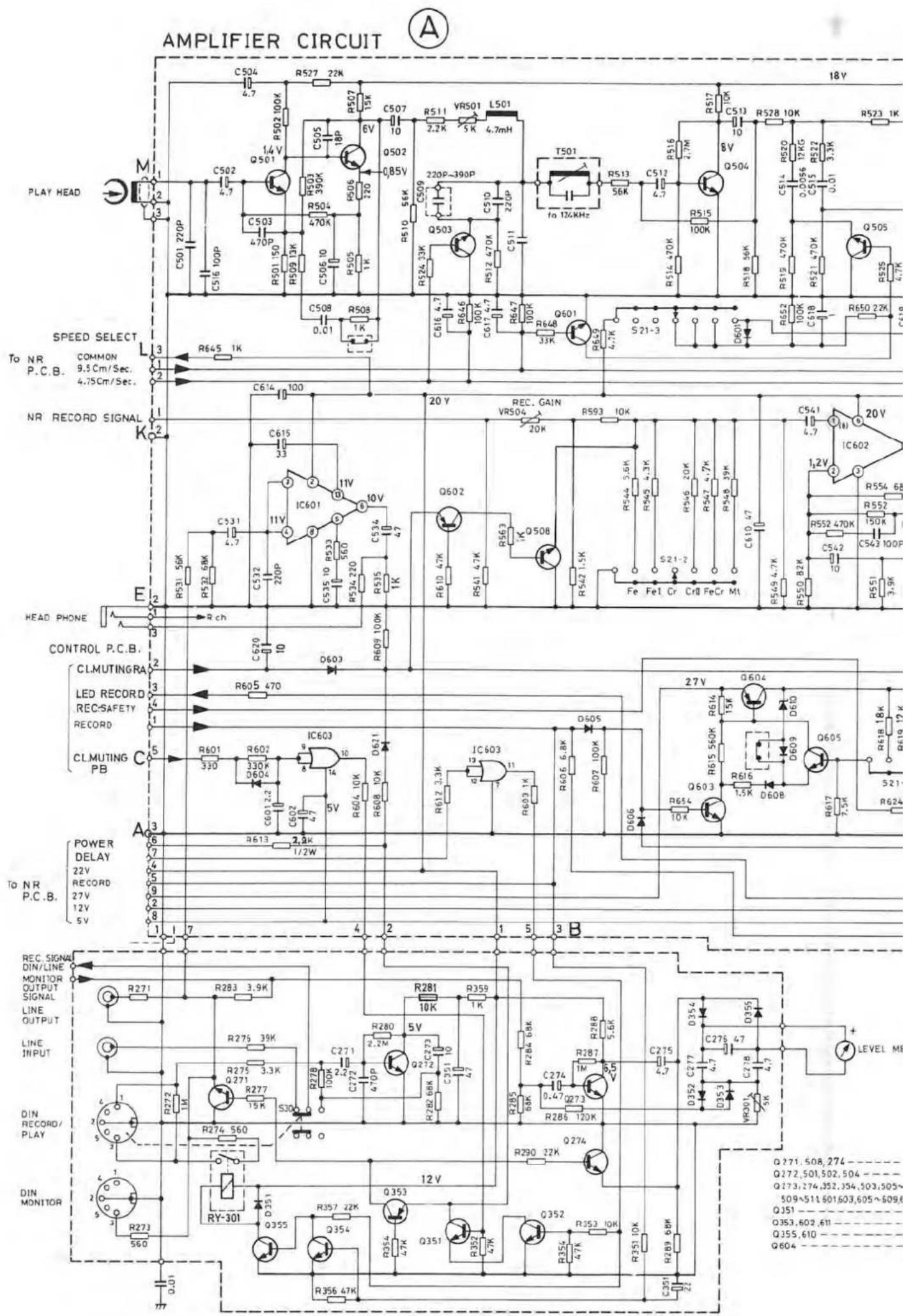
The voltage induced in the playback head (approximately 300 μV during playback of the DIN reference level) is first of all amplified by Q 501 and Q 502 and correspondingly equalized with the negative feedback network R 509, R 508 and C 508. The frequency response at 4 kHz can be slightly modified by closing or opening the strap J 1. The high frequency range can be corrected by replacing the capacitor C 509 (plug-in type). In the case of the 9.5 cm/s tape speed, the playback frequency response is corrected within the 20 kHz range with VR 501 and L 501. VR 501 should not be adjusted. Adjustment is carried out at the factory. The basic position of VR 501 is the middle position.
Changeover of the equalization from 120 μs to 70 μs is realized by the tape type selector switch S 21 - 3 which causes Q 505 to become forward-biased. At the 9.5 cm/s speed, transistor Q 506 switches over to 35 μs whilst Q 601 renders transistor Q 505 reverse-biased. During playback of the Dolby reference level (200 nWb/m), the playback level at LINE OUT is set to 550 mV with the VR 502.
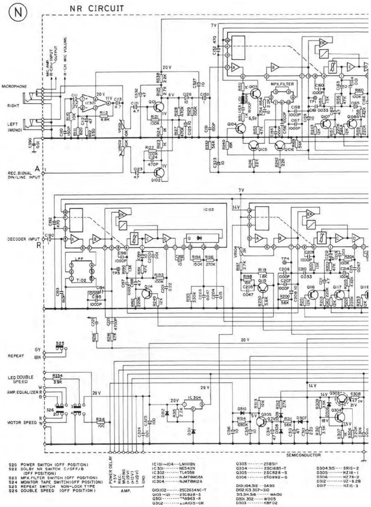
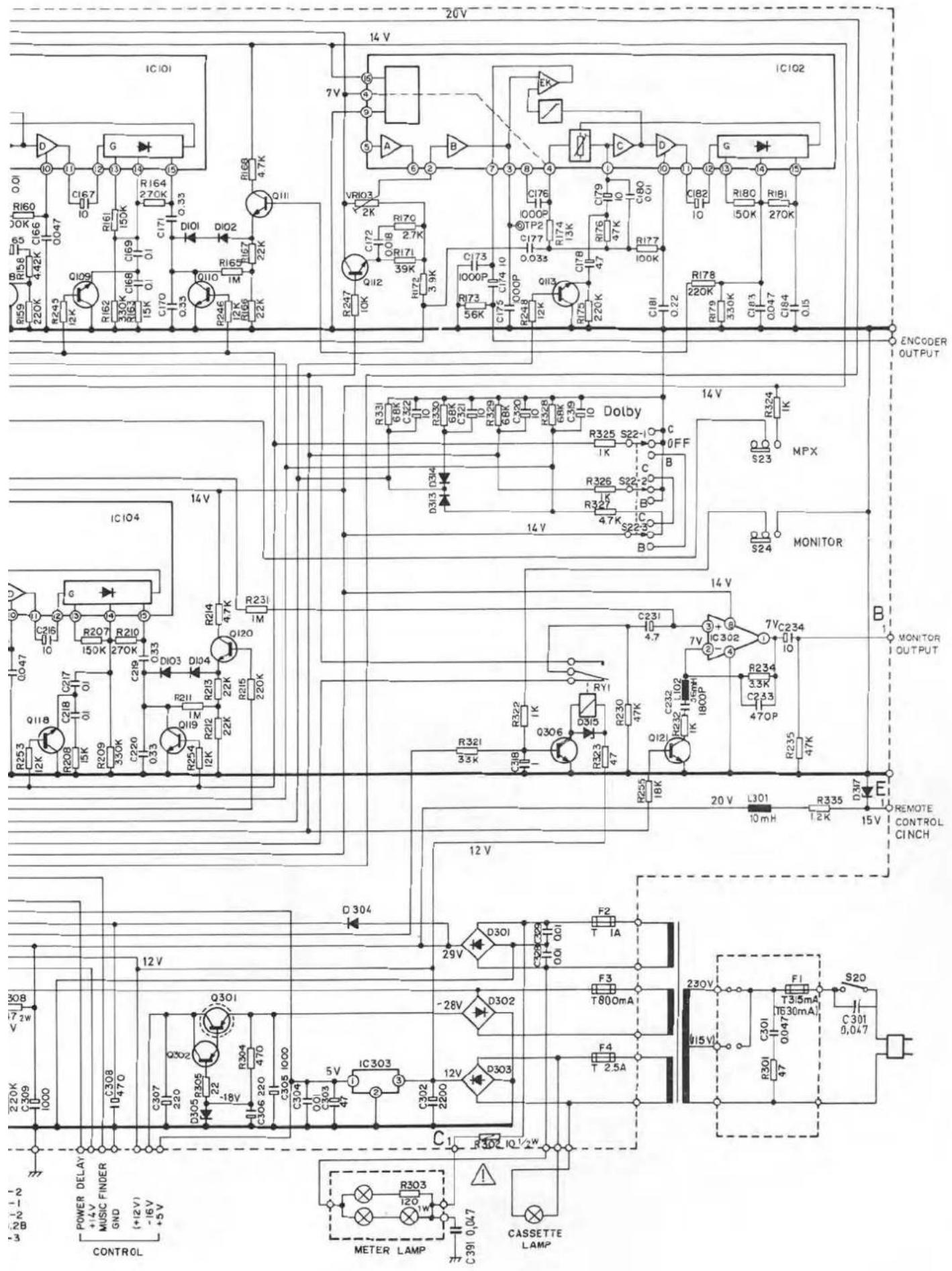
The playback signal is routed through the stopper circuit T 501, Q 504 and VR 502 to the input of the Dolby circuit IC 103, Pin 5. If the Dolby selector switch S 22 is switched off (Q 114 forward-biased), the signal is amplified in a linear manner by approximately 26 dB within the Dolby circuit whilst amplification is frequency and level-dependent when the Dolby circuit is switched on. The output signal is routed from pin 7 (IC 103) to the input pin 2 (IC 104) of the Dolby circuit via VR 104. Also in this case, when the Dolby circuit is switched off (Q 116 forward-biased), the signal is amplified by approximately 26 dB in a linear manner (referred to the input level Pin 5, IC 103). The output signal is routed from Pin 7 (IC 104) to the relay RY 1 which realizes the source-tape monitor function. During playback, RY 1 and the monitor switch S 24 are inoperative and, irrespective of the position of the monitor switch, the tape signal is routed through the amplifier IC 302 to the outputs DIN, LINE and MON. The playback signal is also routed through R 531 from the LINE OUTPUT to the headphone amplifier IC 601 and through R 284 to the VU meter amplifier Q 273.
In order to prevent switching noises from reaching the output sockets, the output signal is muted with Q 271 (see "muting") when the following functions are selected: stop, pause, record, standby, fast forward and rewind.
AFC compensation for IC 104 is realized with the transistor Q 120. Q 120 is controlled by IC 103.
Music finder
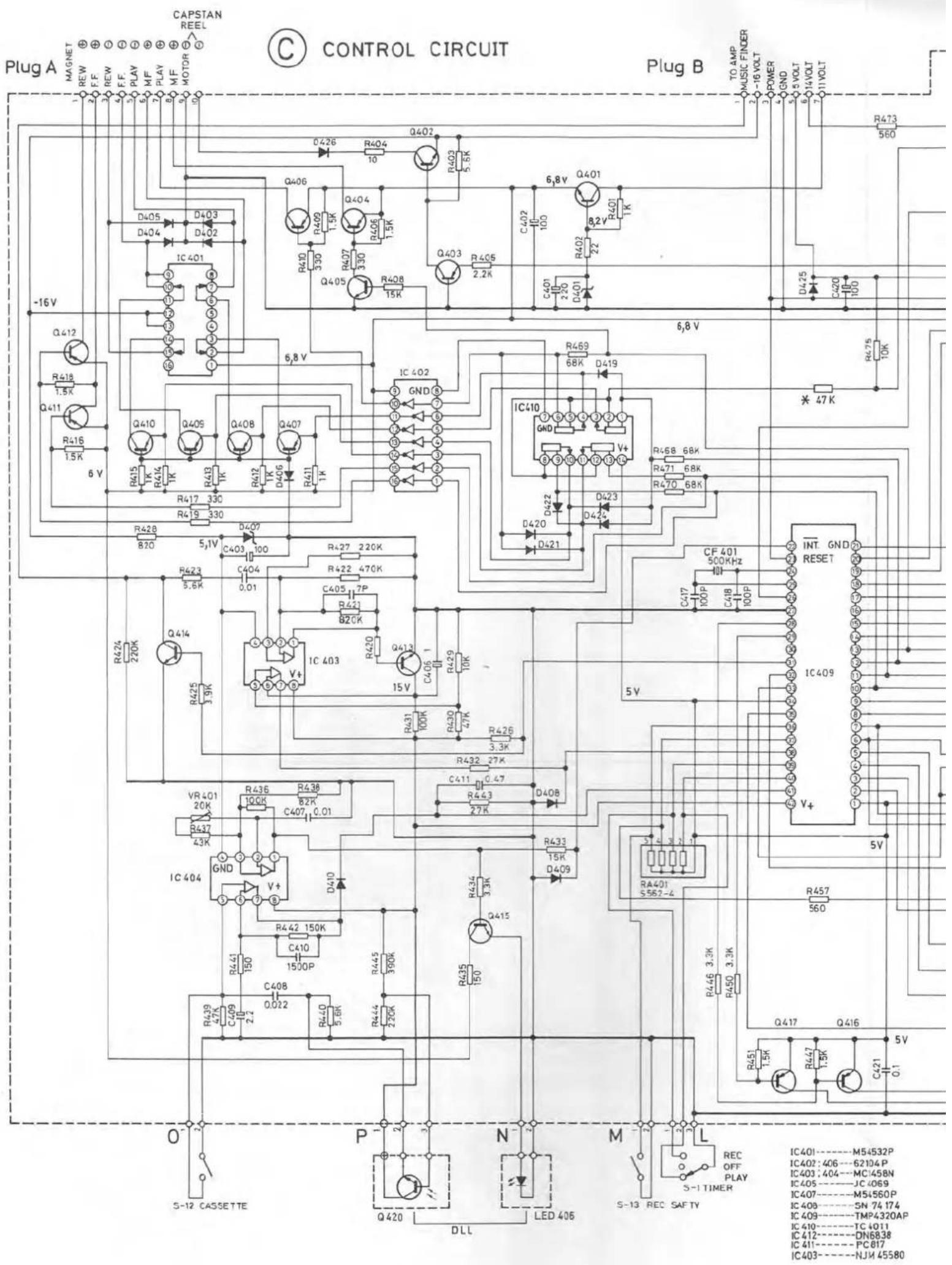
The music finder scan signal (active LOW, IC 409, Pin 31) is routed from the processor to transistor Q.414, this becomes reverse-biased and enables the input of the music finder amplifier IC 403, Pin 2. The AF signal is picked up by the Dolby circuit IC 103, Pin 3 and is amplified with IC 403. From the output (Pin 1), the signal is routed through transistor Q.413, which operates as a limiter, to Pin 6 of IC 403. IC 403 (Pins 5,6,7) operates as a flipflop.
A static signal is applied at the output Pin 7 and, as the result of this, PIECE OF MUSIC is active HIGH. If a SPACE is recognized between the pieces of music, the output changes from HIGH to LOW. This signal is routed to Pin 38 of the processor IC 409 via R 432.
Recording
Three different sources are available for recording. The LINE input is switched off when the DIN socket is used. The signal at the Mic input is amplified by the low-noise IC 301, whilst the signal from the DIN input is amplified by Q 272. The Mic signal is routed to the recording level control VR 101 and the DIN or LINE signal is routed to the recording level control VR 102, both of which act on the mixing amplifiers Q 101 and Q 102. From here, the signal is routed to the input Pin 5 of the Dolby circuit IC 101. With the MPX switch S 23, the MPX filter is connected via transistor Q 105 and Q 106 (both forward-biased) in order to suppress any existing pilot tone residues when recording radio broadcasts. The Dolby circuit is switched on by rendering Q 107 reverse-biased (S 22 set to position B).
AFC compensation is carried out for IC 101 with transistor Q 111. Q 111 is controlled by IC 102.
In order to prevent interference of the Dolby circuit when recording, the high frequency components as from 10 kHz (-3 dB) to 20 kHz (-12 dB) are attenuated by the skewing filter (C 153 and L 101). When the Dolby selector switch S 22-2 is set to position C, the filter is connected with the transistor Q 104 (forward-biased). A HIGH active control signal is applied to the base of Q 104.
In the playback branch, treble attenuation is corrected with the deskewing circuit C 252 and L 102 at the output amplifier IC 302. This circuit is activated with Q 121 (forward-biased) in Dolby C mode.
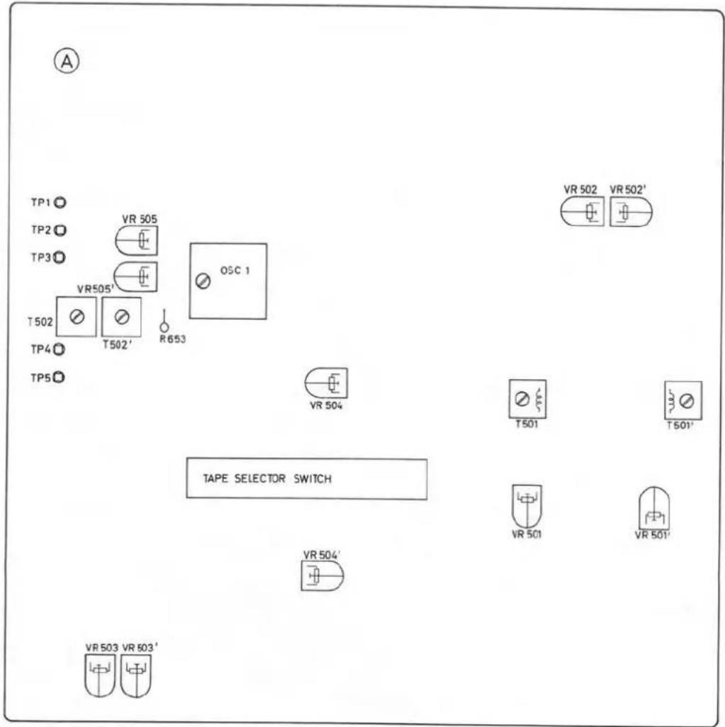
Within the Dolby processor, the signal is branched to two different outputs, Pin 3 and Pin 7 of IC 101. The signal from Pin 3 which is not influenced by the Dolby process is routed to the monitor relay R 41 when the source setting is selected and used as the source signal. The signal from Pin 7 is routed through VR 103 to the input Pin 2 of the Dolby circuit IC 102. During Dolby B mode, C mode is switched off by Q 113 (forward-biased). The output signal of Pin 7 (IC 102) is routed through VR 504 directly to the recording amplifier IC 602. The recording current is set with VR 504. Depending on the tape type, the level (sensitivity) is set with the tape type selector switch S 21-2 and the equalization is set with S 21-1. Additionally, and due to the tape speed of 9.5 cm/s, the equalization time constant is switched over with Q 509 and Q 511 (both forward-biased). When the tape speed of 4.75 cm/s is selected, Q 510 is forward-biased and Q 509 and Q 511 are reverse-biased. The recording signal is routed to the recording head through the stopper circuit T 502. The bias is mixed to it with VR 505.
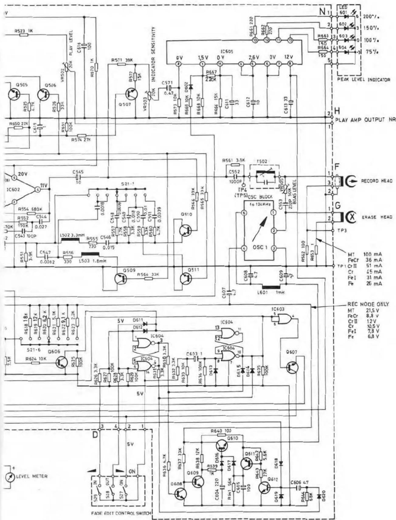
By connection of the resistors R 618 to R 623 with the type type selector switch S 21-6, Q 605 controls transistor Q 604 which influences the oscillator OSC 1 in such a way that an optimum operating point is achieved for the various tape types. The erasure current can be changed with the strap over diode D 609. With transistor Q 603 (record = HIGH signal at the base), Q 604 becomes forward-biased and a voltage of approximately 27 V is applied to the transistor Q 610. The record HIGH signal is also routed through R 606 and D 618 to Q 612 which renders Q 611 forward-biased. Via diode D 617, transistor Q 610 becomes forward-biased due to the switching of Q 611 and the former transistor activates the oscillator OSC 1. The DIN output is switched off with relay RY 301 during recording mode.
Fade edit
With the pushbutton S 27 ON, the supply voltage is applied to IC 604 and, via C 603, the flipflop IC 604 is set to its defined initial position. (Pin 3 LOW, Pin 4 HIGH, Pin 10 LOW). The pushbutton ON must remain depressed for all following FADE EDIT functions.
Fade out: When the pushbutton S 28 (OUT) is operated, a HIGH level is applied to Pin 6 of IC 604. The output Pin 3 changes to HIGH and thus Q 603 becomes forward-biased, Q 609 becomes reverse-biased and a positive voltage builds up at the base of Q 610. The time-determining factor is C 604. Depending on the base voltage, Q 610 becomes forward-biased and thus determines the amplitude of the erasure current. With the HIGH level from S 28 via D 612 at Pin 13 of IC 604, the output Pin 10 changes from LOW to HIGH, Q 607 is switched on with HIGH via IC 603 and the red LED RECORD lights up. The HIGH signal from Pin 10 is also routed through D 606 to Q 603 which switches on the oscillator.
Fade in: When the pushbutton 29 (IN) is operated, a HIGH level is applied to Pin 1 of IC 604, the output Pin 3 changes to LOW, thus Q 608 becomes reverse-biased and Q 609 connects C 604 via R 639 to O V. Via the diode D 620, the HIGH level is routed from the output Pin 4 (IC 604) via the differentiator C 606 to Q 612 which briefly causes Q 611 to become forward-biased and thus charges up C 605. Q 611 becomes reverse-biased and C 605 is discharged via R 641. Thus, a positive voltage with a decreasing level is applied to the base of Q 610 which becomes reverse-biased depending on the base voltage and thus causes the erasure current to decrease.
When the pushbutton ON (S 27) is released, Q 607 (LED RECORD is extinguished) and Q 603 becomes reverse-biased and the oscillator is switched off. In order to prevent the inadvertent erasure of music cassettes (erasure tab removed) with the fade edit facility, transistor Q 606 is forward-biased (HIGH signal at the base = record safety contact open) and thus the flipflop IC 604 is prevented from functioning.
Monitor
During playback (Q 306 reverse-biased), the relay RY 1 is idle and the off tape signal from IC 104 Pin 7 is directly switched to the output amplifier IC 302. In recording mode, the signal from IC 101 Pin 3, which is uninfluenced by the Dolby process, is routed as the source signal to relay RY 1. Due to the signal RECORD (HIGH active) at the base of Q 306, this becomes forward-biased, relay RY 1 is energized and switches over to the source. In this way, the monitor switch S 24 begins to function. If the deck is switched over to "tape", S 24 applies a LOW signal to the base of Q 306 and this becomes reverse-biased. Relay RY 1 is de-energized and switches to "tape". In this way, the information already recorded on the tape can be monitored. As crosstalk of the bias within the record/playback head is unavoidable in this operating mode, the bias must be suppressed by the filter T 501.
Muting, Auto-Space
The recording amplifier and the LED peak display are muted during all functions except RECORD. This control signal MUTING RA (record
amp) is active HIGH and is routed from the device control via connector C (board A) Pin 2 to Q 602 which connects the input of the recording amplifier IC 602 to 0 V via Q 508. Also during recording and when AUTO SPACE is operated, this control signal creates the music space lasting approximately 4 s.
Muting of LINE OUT and MONITOR is realized by the forward-bias of transistor Q 271 (HIGH signal at the base). The processor routes the control signal MUTING playback to board A, connector C, Pin 5 as a LOW active signal during the following functions: stop, rewind, fast forward, music finder ▶ and ◀ and pause.
DIN output switched off = relay RY 1 idle, the contacts are open, transistor Q 355 is reverse-biased, as Q 354 becomes forward-biased due to the RECORD command (HIGH active).
CLEAR MUTING playback = enabling of muting during the following functions: play, record SB (standby) and record. The control signal CLEAR MUTING playback (HIGH active) produced by the processor is routed through connector C (board A) Pin 5 to IC 603, the output Pin 10 of which changes to HIGH with a delay (C 601) and transistor Q 351 becomes forward-biased. Due to AND gating with Q 352, the muting transistor Q 271 cannot become reverse-biased via Q 353 until Q 352 is forward-biased. Q 352 is always forward-biased when the voltage of the power supply unit is at its correct level, HIGH signal at connector C (board A) Pin 7. The output Pin 11 of IC 603 applies a HIGH level to the base of Q 352. This control signal is also routed to the base of Q 355, this becomes forward-biased and switches on the relay and the DIN output is connected into the AF signal. If the RECORD command is issued (HIGH active), Q 354 becomes forward-biased and thus renders Q 355 reverse-biased. The DIN output is disconnected.
Recording level indications
VU: The LINE OUT output signal is amplified with the display amplifier Q 273 via R 284 and routed to the VU meter via the full wave rectifier. The full wave rectifier ensures a precise indication and the VU meter operates with damped return. VU is set for the 0 dB reference level with VR 271. The transistor Q 274 mutes the instrument during all LINE OUT muting functions.
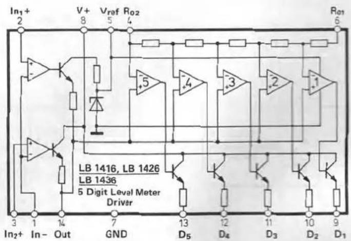
Peak level: The tape type-dependent and treble equalized signal is decoupled from the output of the recording amplifier IC 602 Pin 4 with C 545 and routed via the control VR 503 to the input Pin 2 of the integrated display amplifier IC 605 which directly drives the LED's with its outputs. With transistor Q 507 (forward-biased), the sensitivity is switched over when the tape type selector switch S 21-3 is set to MET. The display is inertialess with 5 LED's which indicate the magnetization of the tape as a percentage.
Device control
Processor
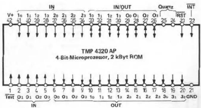
All device and drive functions are controlled by a 4-bit microcomputer with integrated 2 kbyte program memory. The clock frequency is approximately 500 kHz with CF 401 at Pins 24 and 25 of the processor IC 409.
Reset
When the deck is switched on, the supply voltages stabilize to their nominal values. With this LOW-HIGH edge at the reset input Pin 23 of IC 409, the program counter of the precessor is set to its start address and the processor is enabled for its functional sequences. Via D 418 and C 417, a clear pulse is routed to the D flipflop IC 408 Pin 1.
Inputs
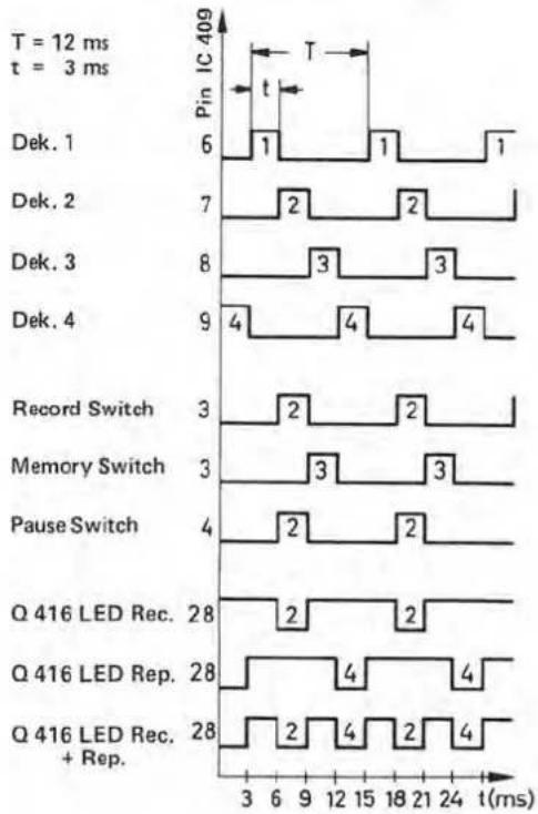
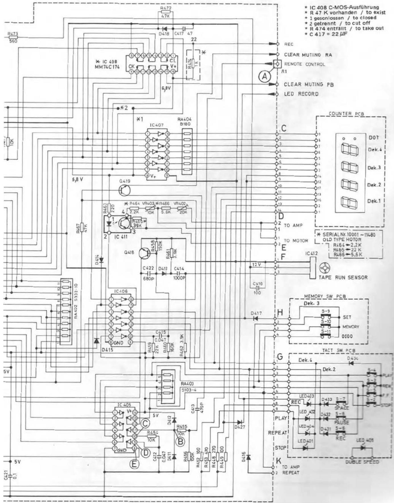
The drive and memory control buttons are interrogated and processed by the processor in the form of a clocked switch matrix. The positive pulses of IC 409 produced at Pin 7 (decade 2) to Pin 9 (decade 4), which are inverted with IC 406, serve as the working clocks. These pulses have a mutual offset of 3 ms (see pulse diagram). When a drive control button is operated, the signal is applied as a HIGH active pulse (inverter IC 405) to the processor IC 409.
The contact sensor S 13 RECORD SAFETY (erasure block) is open when a musicassette is inserted = HIGH signal. In this case, the processor ignores operation of the RECORD button.
The timer switch S 1 routes its inputs PLAY or REC as LOW active signals to the processor.
DLL
The no-contact infrared light barrier system is applied. The infrared emitter LED 406 is driven by the free oscillating oscillator IC 404 from Pin 1 via Q 415. The clock frequency is 1050 Hz and can be varied with VR 401. This frequency is also routed to Pin 22 of the processor as the reference frequency (see also end of tape switch-off). This clocking principle ensures perfect resistance to constant light and interfering reflections. The light pulses are converted to electrical pulses by the phototransistor Q 420 and these are processed by the comparator IC 404. If the light barrier is obstructed (DLL ON), a wave-shaped HIGH level is applied to the output of IC 404 Pin 7 for the duration of the obstruction and this is converted to LOW level with R 443, C 411 and D 410. This LOW signal also occurs when the cassette sensor S 12 is closed (cassette removed). Due to the LOW signal at Pin 41 (IC 409), the processor recognizes DLL ON = cassette removed. The stop function is executed, the LED STOP flashes and, in recording mode, the RECORD function is cancelled. When the deck is set to PLAY, this operating state is stored after removal of the cassette.
End of tape switch-off
The information that the tape is running is passed on to IC 412 by a multiple magnetic disc secured to the drive wheel of the take-up wheel. This IC converts the alternating magnetic fields into electrical pulses. These pulses are routed through C 414 to transistor Q 418 which operates as a flipflop together with IC 406 Pins 7/10. The signals shaped in this way are routed through R 457 to Pin 37 of IC 409. This tape-running frequency is compared by the processor with the 1050 Hz frequency of the oscillator IC 404 which is applied to Pin 22 (IC 409). If the tape-running pulses fail within a period of 1 s, e.g. due to a tape jam, STOP is triggered off. In the event of tape-running malfunctions, the 1050 Hz (±5%) frequency should also be checked, as this serves as the reference frequency for switching off at the end of the tape.
Outputs
The outputs for the device functions (magnets and motors) are issued by the processor as HIGH active signals. The course of the signals for FF (fast forward) is used here as an example. The active HIGH signal of the processor (Pin 10, IC 409) is routed to both the inverting driver IC 402, Pin 1, and to the NAND gate IC 410, Pin 9. With the LOW signal at the output of IC 402, Pin 16, transistor D 412 becomes forward-biased and applies the positive voltage of approximately 6 V to the FF magnet. At the same time, the processor (IC 409, Pin 19 = U BAT) stores the overexcitation signal in the D latch IC 408 Pin 6 for the duration of approximately 100 ms. This time signal (HIGH active) is routed from the output Pin 7 to the NAND inputs of IC 410. The FF command is applied as a HIGH signal to Pin 9 of IC 410. For the duration of the time signal (100 ms) at Pin 8, the output Pin 10 changes to LOW, the inverting driver IC 402 causes transistor Q 409 to become forward-biased with HIGH and drives the driver stage IC 401 Pin 11. Via Pin 10, IC 401 applies the overexcitation voltage of -16 V to the FF magnet.
After the time signal U BAT (100 ms) has elapsed, the diode D 404 holds the magnet until Q 412 switches off. This overexcitation ensures rapid and reliable response of the magnets. Repeated overexcitation of magnets already switched on is suppressed with the coupling diodes D 419 to D 424. Example: The LOW signal FF at the output Pin 10 (IC 410) is routed via D 423 to the AND input Pin 1 and thus disables overexcitation of the magnet PLAY which is being held.

The dynamic HIGH pulses produced by Pin 14 to Pin 20 (IC 409) are converted to static HIGH signals by the D-latch IC 408. The information pending at the D input is written into the clock input Pin 9 (IC 408) by a HIGH pulse (approximately 10 s ) and is available in static form at the Q output until new information is stored.
Capstan motor, reel motor
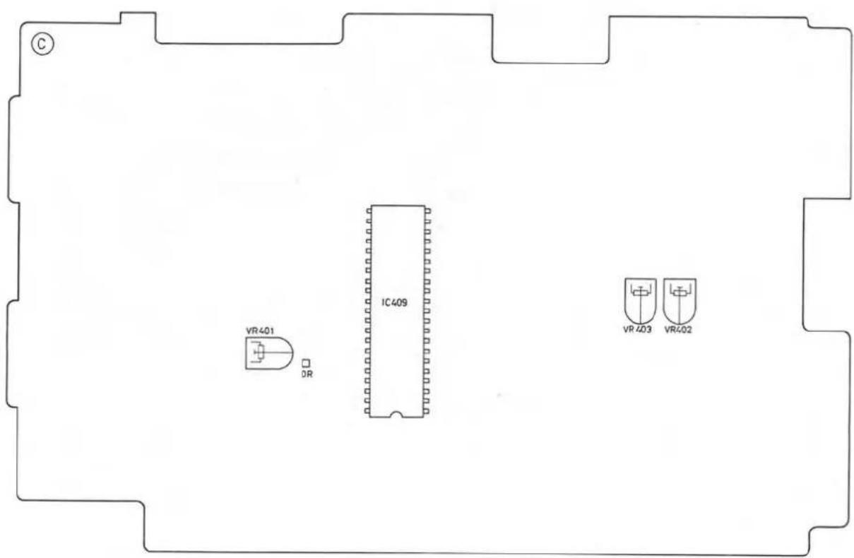
With a HIGH signal from the processor (IC 409, Pin 16), which is stored in the D-latch IC 408, Q 403 causes the transistor Q 402 to become forward-biased and this applies the operating voltage of -16 V to the Capstan motor and reel motor, connector A (board C) Pin 10. The reference voltage for the tape speed is set with VR 403 (9.5 cm/s) and VR 402 (4.75 cm/s). The phototransistor in IC 411 is always forward-biased and only functions when the rewind speed REW is regulated. The flywheel of the Capstan drive is implied via an intermediate linkage for the FF or REW function. In order to prevent excessive stressing of the tape at the end of the reel, - during the function REPEAT = REW and 9.5 cm/s - the rewinding speed is slowed down towards the end of the reel via the optocoupler IC 411. The signals of the tape run sensor IC 412 are evaluated by the processor. If the pulse frequency rises above 75 Hz, LOW active regulation pulses are routed from Pin 33 (IC 409) through D 415 to the inverter IC 406, Pin 2. The HIGH pulses from the output Pin 15 control the photodiode in the optocoupler IC 411. With each positive pulse, the integrated phototransistor becomes reverse-biased and increases the reference voltage via R 465. The Capstan motor is slowed down accordingly. In order to ensure that the tape reaches a high rewinding speed in FF mode, this regulation function is cancelled by a HIGH signal via D 414 and the phototransistor is forward-biased.
Music finder
If the buttons FF or REW are operated during the play function, the processor recognizes the music finder function and routes a LOW signal = SCAN to Pin 31 (IC 409). This signal is routed to transistor Q 414 in order to enable the finder amplifier. The magnets FF and MF (music finder) are energized and, in this way, the double-head only just touches the tape in order to guarantee reliable recognition of the music gap. Wear of the audio head is reduced to a minimum, thanks to this bare touching. If a music gap is now recognized (SPACE = LOW active, see also analog section), this LOW signal is routed to the processor input Pin 38 which initiates the play function.
Auto-space
When the AUTO SPACE button is operated during RECORD mode, the recording amplifier is muted - HIGH signal from Pin 32 (IC 409) to Q 419 - and the tape runs approximately 4 s more until the processor stops the tape and triggers off RECORD STANDBY. With the command PAUSE (HIGH active Pin 20 of IC 409), Q 419 becomes reverse-biased = clear muting playback by a LOW signal via IC 408 and inverter IC 406.
Record standby
If the button RECORD is operated and the contact RECORD SAFETY S 13 is closed (LOW at Pin 36, IC 409), the deck changes over to the function RECORD STANDBY which is indicated by flashing of the green LED PLAY. The magnet PLAY is energized, muting of the playback branch is cancelled (clear muting playback), the Capstan motor is switched on, the recording amplifier is enabled (clear muting RA, Q 419 reverse-biased), the LED PLAY flashes and the LED RECORD lights up. If the button PLAY is now operated, the deck changes over to the record function.
LED display
The functions STOP, PLAY, RECORD, REPEAT and DOUBLE SPEED (9.5 cm/s) are each indicated by one LED. With the exception of DOUBLE SPEED, the LED's are driven on their cathode sides with the LOW active decade pulses (inverter IC 406). The positive operating voltage is connected as pulses with the transistors Q 416 and Q 417. If, for example, the LED RECORD is activated, the processor produces the activation pulses for Q 416 in phase with the pulses of decade 2. If, on the other hand, the LED REPEAT is to light up, the activation pulses for Q 416 are synchronous with the pulses of decade 4.
Counter
The 4-digit display is driven in multiplex mode via inverter IC 406 (decade pulses LOW active) and inverter IC 407 (segment pulses LOW active). Display of the dots for MEMORY and SET is controlled by Q 416 and Q 417.
Pulse Diagramm IC 409
other
| Signal | Time (ms) | |--------|-----------| | Dek. 1 | 6-9 | | Dek. 2 | 7-9 | | Dek. 3 | 8-9 | | Dek. 4 | 9-9 | | Record Switch | 3-9 | | Memory Switch | 3-9 | | Pause Switch | 4-9 | | Q 416 LED Rec. | 28-3 | | Q 416 LED Rep. | 28-3 | | Q 416 LED Rec. + Rep. | 28-3 |Remote control
The IR signals converted to electrical pulses by the infrared receiver are routed via C 413 and inverter IC 405 Pins 11/10 and Pins 9/8 to the input Pin 35 of the processor IC 409.
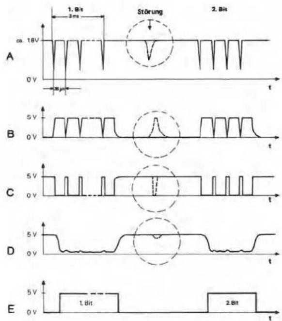
Cause of the signals: A coded command consists of 16 bits. As each transmitted command is repeated for increased reliability, commands consist of 2 x 16 bits = 96 ms duration. One bit corresponds to a length of 3 ms and is clocked with a frequency of approximately 28.5 kHz.
Point A: The clocked bits are applied as voltage fading.
Point B: The signals are differentiated and limited to 5 V with C 413 and R 456 (diodes D 411 and D 412).
Point C: The pulses are negated by the inverter IC 405. Positive needle pulses are now applied.
Point D: The pulses are integrated by R 454 and C 412.
Point E: Inverter IC 405 negates and a positive pulse = 1 bit with a duration of approximately 3 ms is applied at the input of the processor.
This method ensures good suppression of noise pulses. Points A to E are identical with the designations in the circuit diagram.
32 → L Clear Muting RA (Record Amp)
33 → ∪ ∪ Wickelregelung, Reel Control
34 +5V
35← 几処 Remote Control
36← ∫ Record Safety Switch
37←Tape Run Sensor
38← 2 Signal Space (Musiklücke)
39← L Timer Record
40←7 Timer Play
41← 2 DLL IR-System, Cassette Switch
42 U_BAT + 5V
In Function by
Fast Forward, Music Finder ▶▶, Record, Play
Rewind, Music Finder ◀, Record, Play
Pause, Record SB, Play, Record
Play, Record SB, Record
Recod SB, Record
Fast Forward, Music Finder ▶▶
Record SB, Record | Set | Repeat Play, Record SB | Memory | Stop
Record SB = Record Stand By
Transistorentabelle Dolby
● Transistor leitend / turned on = HIGH an Basis
| Transistor | Switch S 22 | ||
| Off | B | C | |
| Q 104 | |||
| Q 107 | |||
| Q 108 | |||
| Q 109 | |||
| Q 110 | |||
| Q 112 | |||
| Q 113 | |||
| Q 114 | |||
| Q 115 | |||
| Q 116 | |||
| Q 117 | |||
| Q 118 | |||
| Q 119 | |||
| Q 121 | |||
Adjustment instructions C 844
| Signal source | Signal source adjustment | Unit adjustment | Indicator connection | Adjustment position | Adjustment Remarks |
| Azimuth | |||||
| Test cassette 21 | 10 kHz | Fe : ON | AF-voltmeter to OUTPUT | Azimuth screw A | Maximum, lock with lacquer |
| Tape speed 9.5 cm/s, 4.75 cm/s | |||||
| Test cassette 1 | 3150 Hz | Fe : ONDouble Speed : ON | Frequency counter to OUTPUT | © VR 403 | 6300 Hz, -0.5% |
| Double Speed : OFF | © VR 402 | 3150 Hz, -0.5% | |||
| Power : ON | Frequency counter to © Point OR | © VR 401 | Adjust to 1050 Hz | ||
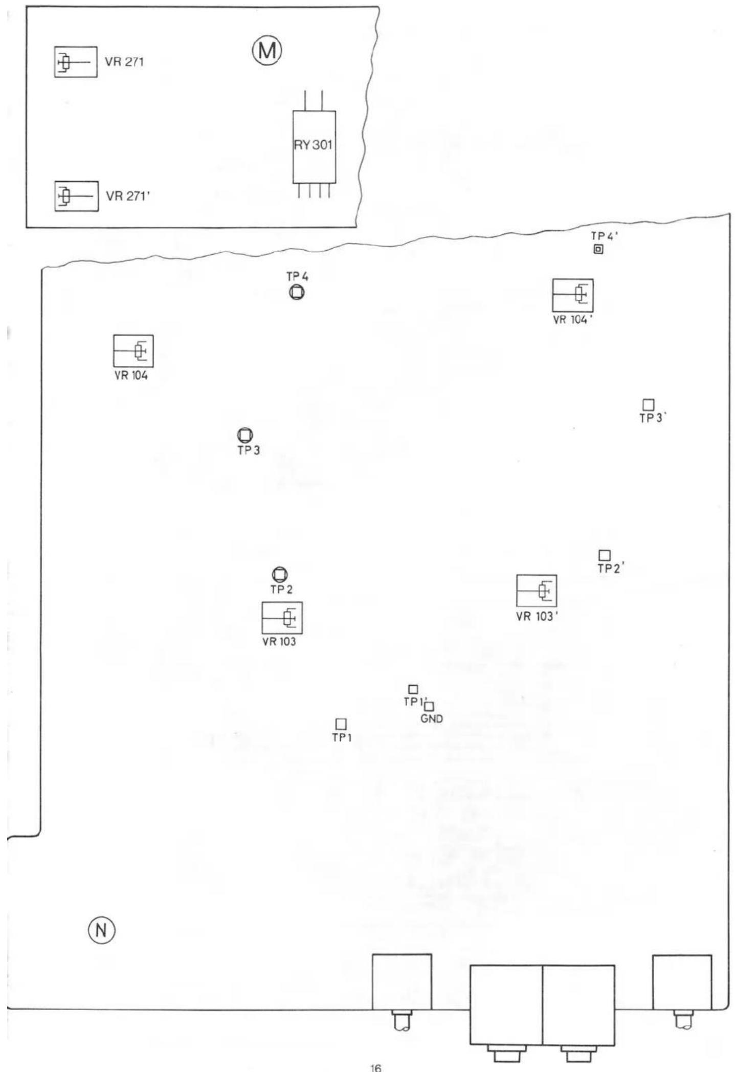
| AF-generator to INPUT LEFT and RIGHT | 400 Hzapp.100 mV | Fe : ONRecord : ON | AF-voltmeter to TP 1TP 1' | Record Level | Adjust to 580 mV |
| AF-voltmeter to TP 2TP 2' | N VR 103VR 103' | Adjust to 580 mV | |||
| Test cassette 21 | 400 Hz Dclby-level 200 nWb/m | Fe : ONPlay : ON | AF-voltmeter to TP 3TP 3' | A VR 502VR 502' | Adjust to 580 mV |
| AF-voltmeter to TP 4TP 4' | N VR 104VR 104' | Adjust to 580 mV | |||
| Playback level | |||||
| 400 Hz Dclby-level 200 nWb/m | Fe : ON | AF-voltmeter to OUTPUT LEFT/RIGHT | A VR 502VR 502' | Adjust to 550 mV | |
| Level indicator VU, Peak LED | |||||
| AF-generator to INPUT LEFT and RIGHT | 400 Hzapp. 100 mV | Fe : ONRecord : ON | AF-voltmeter to OUTPUT LEFT/RIGHT | Record Level | 550 mV Output |
| M VR 271VR 271' | VU-indicator adjust to 0 db VU | ||||
| AF-generator to INPUT LEFTINPUT RIGHT | Cr : ONRecord : ON | A VR 503VR 503' | LED-indicator adjust to 150 % | ||
| Oszillator, RF-traps | |||||
| Metal : ONRecord : ON | Frequency counter A to R 653 | A OSC 1 | 124 kHz | ||
| AF-voltmeter to TP 4TP 5 | A T 502T 502' | Minimum HF | |||
| Metal : ONMonitor : ONRecord : ON | AF-voltmeter to OUTPUT LEFT/RIGHT | A T 501T 501' | |||
| Erasing voltage | |||||
| Metal : ONRecord : ON | AF-voltmeter and Oszilloscope to R 653 | Jumper about A D 609 | app. 100 mV when the signal is clipping to cut off jumper | ||
| RF-magnetic biasing | |||||
| AF-generator to INPUT LEFT and RIGHT | 400 Hz / 10 kHzapp. 100 mVBASF C-401 R or BASF C 60Chromdioxid | Cr : ONRecord : ON | AF-voltmeter to OUTPUT LEFT/RIGHT | Record Level | app. 30 mV Output |
| Cr : ONMonitor : ONRecord : ON | A VR 505VR 505' | Adjust to level symmetrie o playback at test frequencyAt treble emphasis:turn clockwiseAt treble de-emphasis:turn counterclockwise | |||
| Record Level | |||||
| AF-generator to INPUT LEFT and RIGHT | 400 Hzapp. 100 mVBASF C 60Chromdioxid | Cr : ONRecord : ON | AF-voltmeter to OUTPUT LEFT/RIGHT | 550 mV Output | |
| Cr : ONMonitor : ONRecord : ON | A VR 504VR 504' | Adjust to 550 mV | |||
| 74----2SC2878-B | IC601---LA4170 |
| 2,504----2SC2634NC-T | IC602---NE542N |
| 2,354,503,505~507 | IC603---MB84071BM |
| 1,603,605~609,612-2SC828-S | IC604---MB84001BM |
| ----2SC628A-S | IC605---LB1436 |
| 25D892-Q | D351-353,601-606 |
| 2SA683NC-S | 608,609,611-621--MA150 |
| D354,355----OA90 | |
| DE10----HZ6A-1L | |
| LED601,602----GL9PR12 | |
| LED603,604----GL9NG12 |
532P
14P
458N
069
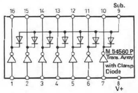
560P
74 174
4320AP
011 938
317
145580
Q401----25D837R
Q402-2SD893R
Q403.407\~410.416.417---2SAIO15GR
Q404.406.411.412----2SA1020Y
Q405,413\~415,418,419---2SC1815GR
Q420 PN108
D401----HZ9A-2
D402\~405.425---SR1S-2
D415----IN60P
D407----HZ5C-2
D406,408-414
416-425, 427----US1035
D431-434----MA150
LED401403----TLR124
LED 402,504 505--TLG 124
LED 406----LN55
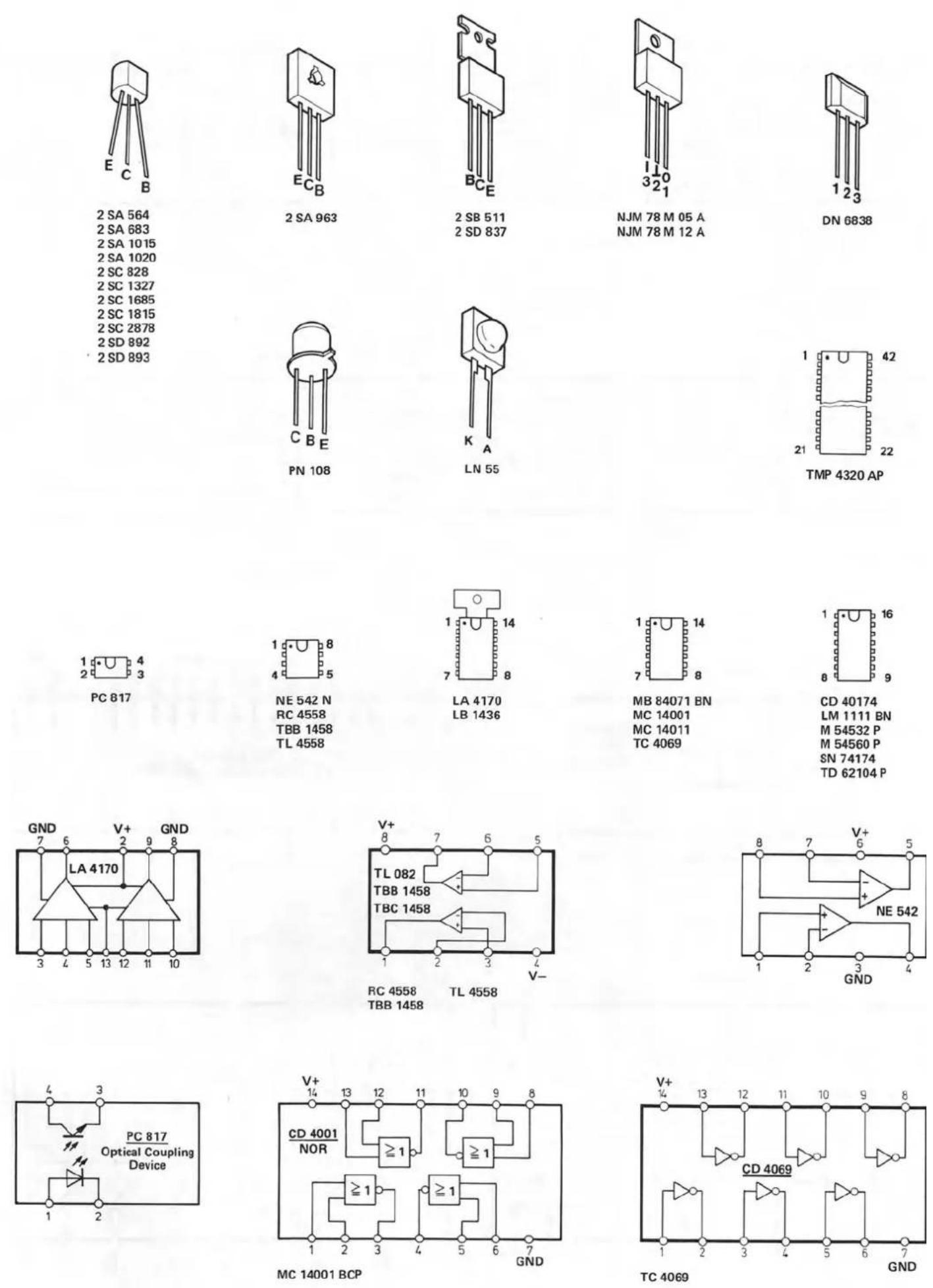
2 SA 564
2 SA 683
2 SA 1015
2 SA 1020
2 SC 828
2 SC 1327
2 SC 1685
2 SC 1815
2 SC 2878
2 SD 892
2 SD 893
2 SA 963
2 SB 511
2 SD 837
NJM 78 M 05 A
NJM 78 M 12 A
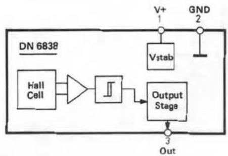
DN 6838
PN 108
LN 55
TMP 4320 AP
PC 817
NE 542 N
RC 4558
TBB 1458
TL 4558
LA 4170
LB 1436
MB 84071 BN
MC 14001
MC 14011
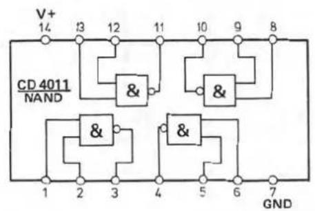
TC 4069
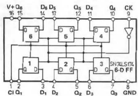
CD 40174
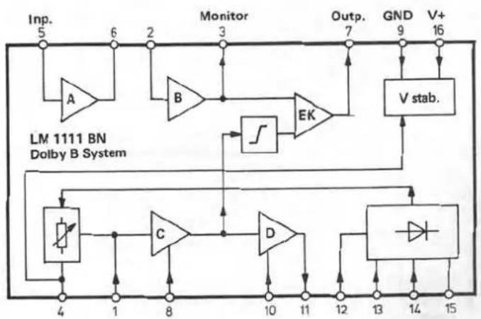
LM 1111 BN
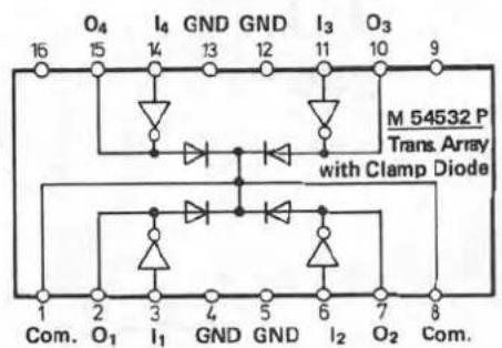
M 54532 P
M 54560 P
SN 74174
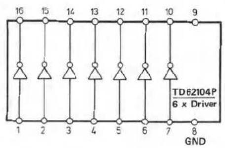
TD 62104 P
RC 4558
TBB 1458
TL 4558
MC 14001 BCP
TC 4069
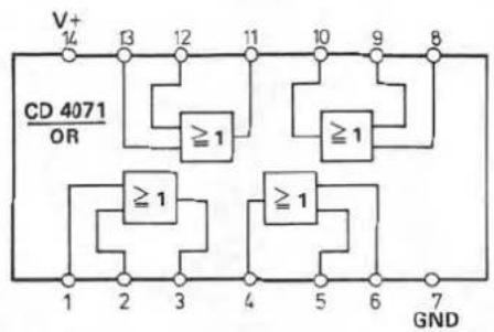
flowchart
graph TD
    A["Pin 1"] --> B["≥1"]
    C["Pin 2"] --> D["≥1"]
    E["Pin 3"] --> F["≥1"]
    G["Pin 4"] --> H["≥1"]
    I["Pin 5"] --> J["≥1"]
    K["Pin 6"] --> L["≥1"]
    M["Pin 7"] --> N["≥1"]
    O["V+"] --> P["Pin 14"]
    Q["CD 4071/OR"] --> R["≥1"]
    S["GND"] --> T["≥1"]
    U["Pin 8"] --> V["≥1"]
    W["Pin 9"] --> X["≥1"]
    Y["Pin 10"] --> Z["≥1"]
    AA["Pin 11"] --> AB["≥1"]
    AC["Pin 12"] --> AD["≥1"]
    AE["Pin 13"] --> AF["≥1"]
    AG["Pin 14"] --> AH["≥1"]
MB 84071 BN
flowchart
graph TD
    A["Pin 1"] --> B["&"]
    C["Pin 2"] --> D["&"]
    E["Pin 3"] --> F["&"]
    G["Pin 4"] --> H["&"]
    I["Pin 5"] --> J["&"]
    K["Pin 6"] --> L["&"]
    M["Pin 7"] --> N["&"]
    O["V+"] --> P["14"]
    P --> Q["3"]
    Q --> R["12"]
    R --> S["11"]
    S --> T["10"]
    T --> U["9"]
    U --> V["8"]
    W["GND"] --> X["7"]
MC 14011 BP
flowchart
graph LR
    A["DN 6838"] --> B["Hall Cell"]
    B --> C["J"]
    C --> D["Output Stage"]
    D --> E["Vstab"]
    E --> F["GND 2"]
    D --> G["Out"]
    style A fill:#f9f,stroke:#333
    style B fill:#ccf,stroke:#333
    style C fill:#cfc,stroke:#333
    style D fill:#fcc,stroke:#333
    style E fill:#cff,stroke:#333
    style F fill:#ffc,stroke:#333
    style G fill:#cfc,stroke:#333
flowchart
graph TD
    A["Pin 1"] --> B["Q1"]
    C["Pin 2"] --> D["Q2"]
    E["Pin 3"] --> F["Q3"]
    G["Pin 4"] --> H["Q4"]
    I["Pin 5"] --> J["Q5"]
    K["Pin 6"] --> L["Q6"]
    M["Pin 7"] --> N["Q7"]
    O["Pin 8"] --> P["GND"]
    Q["Pin 9"] --> R["AND Gate"]
    S["Pin 10"] --> T["LED"]
    U["Pin 11"] --> V["D4"]
    W["Pin 12"] --> X["D5"]
    Y["Pin 13"] --> Z["D6"]
    style A fill:#f9f,stroke:#333
    style C fill:#f9f,stroke:#333
    style E fill:#f9f,stroke:#333
    style G fill:#f9f,stroke:#333
    style I fill:#f9f,stroke:#333
    style Q fill:#f9f,stroke:#333
    style R fill:#f9f,stroke:#333
    style S fill:#f9f,stroke:#333
    style T fill:#f9f,stroke:#333
    style U fill:#f9f,stroke:#333
    style V fill:#f9f,stroke:#333
    style W fill:#f9f,stroke:#333
    style X fill:#f9f,stroke:#333
    style Y fill:#f9f,stroke:#333
    style Z fill:#f9f,stroke:#333
    style AA fill:#f9f,stroke:#333
    style AB fill:#f9f,stroke:#333
    style AC fill:#f9f,stroke:#333
    style AD fill:#f9f,stroke:#333
    style AE fill:#f9f,stroke:#333
    style AF fill:#f9f,stroke:#333
    style AG fill:#f9f,stroke:#333
    style AH fill:#f9f,stroke:#333
    style AI fill:#f9f,stroke:#333
    style AJ fill:#f9f,stroke:#333
    style AK fill:#f9f,stroke:#333
    style AL fill:#f9f,stroke:#333
    style AM fill:#f9f,stroke:#333
    style AN fill:#f9f,stroke:#333
    style AO fill:#f9f,stroke:#333
    style AP fill:#f9f,stroke:#333
    style AQ fill:#f9f,stroke:#333
    style AR fill:#f9f,stroke:#333
    style AS fill:#f9f,stroke:#333
    style AT fill:#f9f,stroke:#333
    style AU fill:#f9f,stroke:#333
    style AV fill:#f9f,stroke:#333
SN 74174
CD 40174
flowchart
graph TD
    A["Input: 5"] --> B["A"]
    B --> C["Monitor: 2"]
    C --> D["B"]
    D --> E["EK"]
    E --> F["V stab."]
    F --> G["Output: 7"]
    G --> H["GND: 9"]
    H --> I["V+: 16"]
    J["LM 1111 BN Dolby B System"] --> K["Amplifier 4"]
    K --> L["C"]
    L --> M["D"]
    M --> N["Diode"]
    N --> O["Output: 15"]
    style A fill:#f9f,stroke:#333
    style B fill:#ccf,stroke:#333
    style C fill:#cfc,stroke:#333
    style D fill:#fcc,stroke:#333
    style E fill:#cff,stroke:#333
    style F fill:#ffc,stroke:#333
    style G fill:#fcc,stroke:#333
    style H fill:#ffc,stroke:#333
    style I fill:#fcc,stroke:#333
    style J fill:#ffc,stroke:#333
    style K fill:#cfc,stroke:#333
    style L fill:#cfc,stroke:#333
    style M fill:#cfc,stroke:#333
    style N fill:#cfc,stroke:#333
    style O fill:#cfc,stroke:#333
flowchart
graph TD
    subgraph SOLENOIDS
        A["REW PLAY FF"] --> B["WHITE VIOLET BLACK RED"]
        C["ORANGE"] --> D["BROWN ORANGE"]
        E["GREEN"] --> F["ORANGE"]
        G["BROWN ORANGE"] --> H["ORANGE"]
        I["ORANGE"] --> J["ORANGE"]
    end

    subgraph MF-SOLENOID
        K["BLUE YELLOW"] --> L["CONTROL P.C.B"]
        M["ORANGE"] --> N["ORANGE"]
        O["ORANGE"] --> P["ORANGE"]
        Q["ORANGE"] --> R["ORANGE"]
    end

    subgraph Q401
        S["GREEN YELLOW RED to AMP PC.B (A)"] --> T["ORANGE WHITE GREEN RED BLUE"]
        U["ORANGE"] --> V["ORANGE GREEN RED"]
        W["ORANGE"] --> X["ORANGE GREEN RED"]
        Y["ORANGE"] --> Z["ORANGE GREEN RED"]
        AA["ORANGE"] --> AB["ORANGE GREEN RED"]
        AC["ORANGE"] --> AD["ORANGE GREEN RED"]
        AE["ORANGE"] --> AF["ORANGE GREEN RED"]
        AG["ORANGE"] --> AH["ORANGE GREEN RED"]
        AI["ORANGE"] --> AJ["ORANGE GREEN RED"]
        AK["ORANGE"] --> AL["ORANGE GREEN RED"]
        AM["ORANGE"] --> AN["ORANGE GREEN RED"]
        AO["ORANGE"] --> AP["ORANGE GREEN RED"]
        AQ["ORANGE"] --> AR["ORANGE GREEN RED"]
        AS["ORANGE"] --> AT["ORANGE GREEN RED"]
        AU["ORANGE"] --> AV["ORANGE GREEN RED"]
        AW["ORANGE"] --> AX["ORANGE GREEN RED"]
        AY["ORANGE"] --> AZ["ORANGE GREEN RED"]
        BA["ORANGE"] --> BB["ORANGE GREEN RED"]
        BC["ORANGE"] --> BD["ORANGE GREEN RED"]
        BE["ORANGE"] --> BF["ORANGE GREEN RED"]
        BG["ORANGE"] --> BH["ORANGE GREEN RED"]
        BI["ORANGE"] --> BJ["ORANGE GREEN RED"]
        BK["ORANGE"] --> BL["ORANGE GREEN RED"]
        BM["ORANGE"] --> BN["ORANGE GREEN RED"]
        BO["ORANGE"] --> BP["ORANGE GREEN RED"]
        BCI["ORANGE"] --> CB["ORANGE GREEN RED"]
        CC["ORANGE"] --> CD["ORANGE GREEN RED"]
        CE["ORANGE"] --> CF["ORANGE GREEN RED"]
        CG["ORANGE"] --> CH["ORANGE GREEN RED"]
        CI["ORANGE"] --> CJ["ORANGE GREEN RED"]
        CK["ORANGE"] --> CKB["ORANGE GREEN RED"]
        CL["ORANGE"] --> CM["ORANGE GREEN RED"]
        CN["ORANGE"] --> CO["ORANGE GREEN RED"]
        CP["ORANGE"] --> CCL["CINCH OUT"]
    end

    subgraph DIGITAL COUNTER
        D["DIGITAL COUNTER Back Side"] --> E["TAPE RUN SENSOR"]
        F["TAPE RUN SENSOR"] --> G["TAPE RUN SENSOR"]
        H["TAPE RUN SENSOR"] --> I["TAPE RUN SENSOR"]
        J["TAPE RUN SENSOR"] --> K["TAPE RUN SENSOR"]
        L["TAPE RUN SENSOR"] --> M["TAPE RUN SENSOR"]
        N["TAPE RUN SENSOR"] --> O["TAPE RUN SENSOR"]
    end

    subgraph CAPSTAN MOTOR
        P["CAPSTAN MOTOR"] --> Q["CAPSTAN MOTOR"]
        R["CAPSTAN MOTOR"] --> S["CAPSTAN MOTOR"]
        T["CAPSTAN MOTOR"] --> U["CAPSTAN MOTOR"]

    subgraph DLL PN 108
        V["S-12"] --> W["VIOLET BLUE"]
        X["LN 55 DLL"] --> Y["S-13"]
    end

    subgraph REC-SAFETY SWITCH
        Z["S-13"] --> AA["S-1"]
    end

    subgraph TIMER SWITCH
        AB["S-1"] --> AC["S-1"]
    end

    subgraph TOUCH SWITCH
        AD["S-1"] --> AE["S-1"]
    end

    style SOLENOIDS fill:#f9f,stroke:#333
    style MF-SOLENOID fill:#ccf,stroke:#333
    style Q401 fill:#cfc,stroke:#333
    style DIGITAL COUNTER Back Side fill:#fcc,stroke:#333
    style CAPSTAN MOTOR fill:#fff,stroke:#333
    style TOUCH SWITCH fill:#fff,stroke:#333
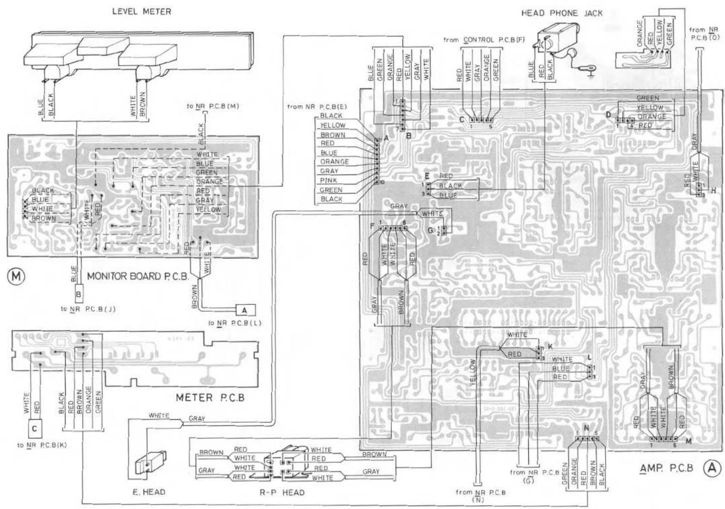
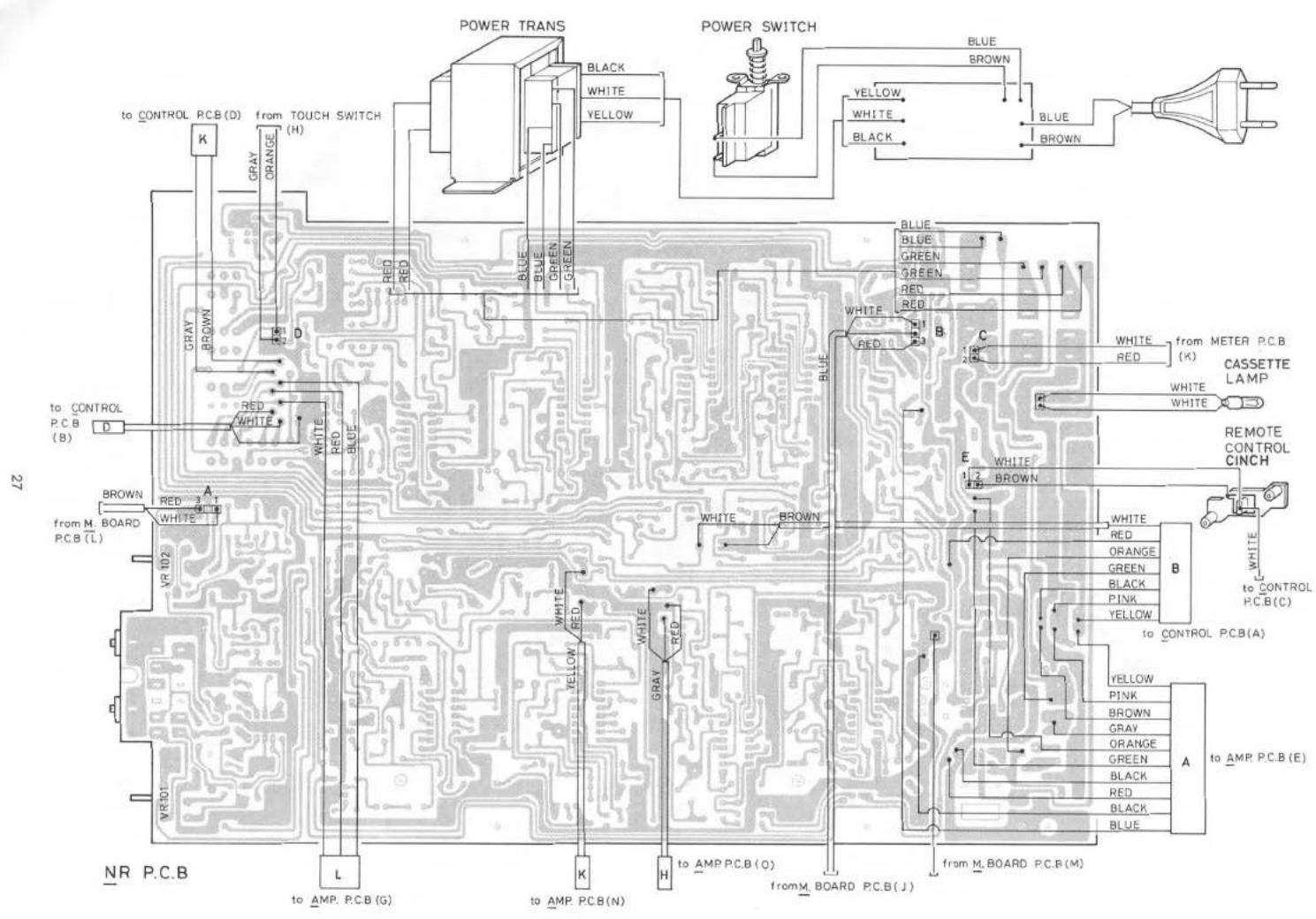

Grundplatte / Base plate / Plaque de base

A.M.P. PARTS LOCATION TOP VIEW
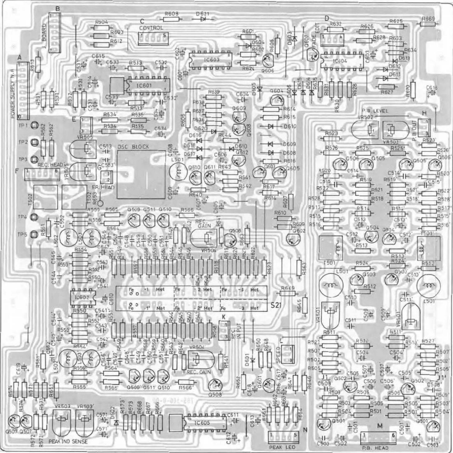

MONITOR PARTS LOCATION TOP VIEW

| Technische Daten (typische Werte)Das Gerät erfüllt bzw. übertrifft die in DIN 45 500 festgelegten Anforderungen an Geräte der Heimstudio-Technik HiFi) | Technical Data (typical values)The unit meets the requirements of DIN 45 500 for domestic HiFi equipment. The data given are based on the current DIN reference tapes. | Caractéristiques techniques (valeurs caractéristiques)Cet appareil surpasse par ses performances les exigences de la norme DIN 45500 (matériel HiFi, grand public). | ||||
| Dolby B | Dolby C | Dolby B | Dolby C | |||
| Bandgeschwindigkeit | Tape speed | Vitesse de la bande | 9,5 cm/s | 4,75 cm/s | ||
| Kurzzeitige Geschwindigkeitsschwankungen (Tonhöhenschwankungen)W.R.M.Snach DIN nur Wiedergabenach DIN Aufnahme/Wiedergabe | Wow and flutterWeighted RMSto DIN / or playback onlyto DIN for recording/playback | Fluctuations instantanées de la vitesse (variations de la hauteur du son)W.R.M.Sselon DIN lecture uniquementselon DIN enregistrement/lecture | 0,02 %0,04 %0,05 % | 0,035 %0,07 %0,10 % | ||
| Übertragungsbereich(bezogen auf DIN-Toleranzfeld)Fe -BandCrO2-BandFeCr-BandReineisen-Band | Frequency response (ref. to DIN tolerances)Standard Fe tapeCrO2 tapeFeCr tapeMetal tape | Bande passante (ramenée à la plage de tolérance DIN)Bande FeBande CrO2Bande FeCrBande fer pur | 20 - 24 000 Hz20 - 24 000 Hz20 - 24 000 Hz20 - 24 000 Hz | 20 - 17 000 Hz20 - 18 000 Hz20 - 19 500 Hz20 - 20 000 Hz | ||
| Ruhageräuschspannungsabstandmit Dolby NRFe -BandCrO2-BandFeCr-BandReineisen-Band | Signal-to-noise-ratiowith Dolby NRStandard Fe tapeCrO2 tapeFeCr tapeMetal tape | Rapport signal/bruitavec Dolby NRBande FeBande CrO2Bande FeCrBande fer pur | 69697171 | 76 dB76 dB78 dB78 dB | 67616969 | 74 dB74 dB76 dB76 dB |
| Übersprechdämpfung (bei 1 000 Hz)zwischen zusammengehörgen Kanälenzwischen Kanälen in Gegenrichtung | Channel separation (at 1,000 Hz)between stereo channelsin opposite direction | Diaphonie (à 1 000 Hz)en sens stéréoen sens inverse | 40 dB70 dB | |||
| Löschämpfung bei 1 000 Hz | Erasure at 1,000 Hz | Attéquation d'effacement à 1 000 Hz | 70 dB | |||
| Oszillator-Frequenz(Gegentaktoszillator) | Oscillator(push/pull: oscillator) | Fréquence de l'oscillateur(oscillateur push-pull) | 124 kHz | |||
| Eingänge (Empfindlichkeit für 0 dB)Mikrofon (1/4" Koax.-Buchse)Receiver/Verstärker (DIN-Buchse)Receiver/Verstärker (RCA-Buchsen) | Inputs (sensitivity at 0 dB)Microphone (1/4" coaxial jack)Receiver/amplifier (DIN connector)Receiver/amplifier (RCA jacks) | Entrées (sensibilité pour 0 dB)Micro (prise coaxiale de 1/4")Ampli-tuner/amplificateur (prise DIN)Ampli-tuner/amplificateur (prises RCA) | 0,4 / 10 mV / kOhm0,5 / 5 mV / kOhm70 / 50 mV / kOhm | |||
| AusgängeReceiver/Verstärker (DIN-Buchse)Receiver/Verstärker (RCA-Buchse)Kopfhärer (1/4" Koax. Buchse) | OutputsReceiver/amplifier (DIN connector)Receiver/amplifier (RCA jacks)Headphones (1/4 coaxial jack) | SortiesAmpli-tuner/amplificateur (prise DIN)Ampli-tuner/amplificateur (prises RCA)Casque d'écoute (prise ciaxiale de 1/4") | 550 / 4 mV / kOhm560 / 4 mV / kOhm4 - 2000 Ohm | |||
| Umspulzeitfür C 60 Cassette | Fast winding timefor C 60 cassettes | Temps de rebobinagepour cassette C 60 | 60 | 105 s | ||
| Bandlaufüberwachung(elektronisch)Abschaltet | Tape monitor(electronic)shut-off time | Contrôle du défilement de bande(electronique)Temps de déclenchement | 1,0 s | |||
| Netzspannung | Line voltage | Tension secteur | 115 V und 230 Voder 115 V | |||
| Netzfrequenz | Line frequency | Fréquence secteur | 50 / 60 Hz | |||
| Leistungsaufnahme | Power requirement | Consommation | 50 W | |||
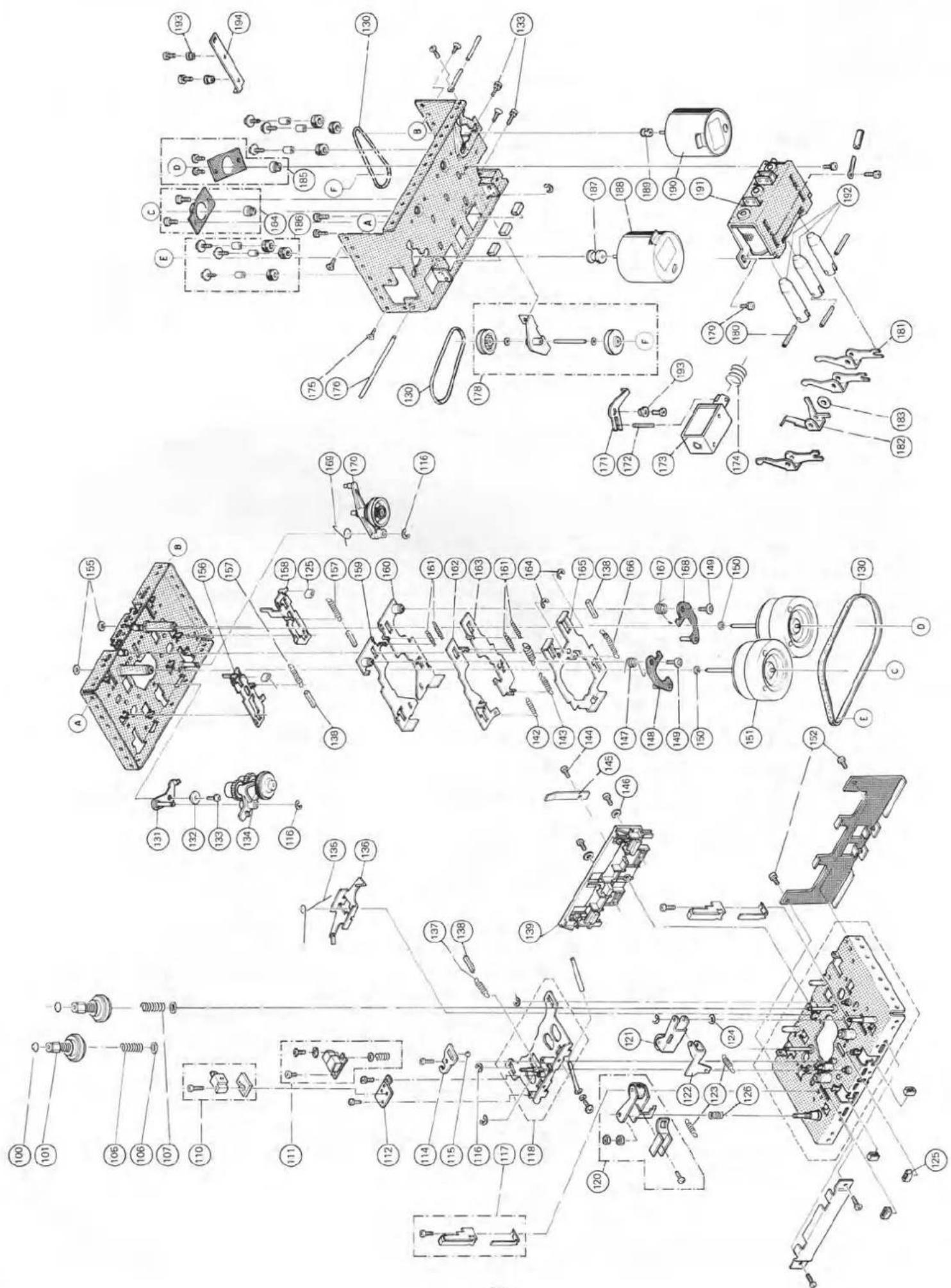
| Pos. | Art.-Nr.Part-No.Réfer | Stok.Qty.ndp. | Bezeichnung | Description | Désignation |
| L 503 | 271 140 | 2 | 3,9 mH | 3,9 mH | 3,9 mH |
| L 601 | 271 141 | 1 | 1 mH | 1 mH | 1 mH |
| S 21 | 270 228 | 1 | Schalter (Tape Selector) | Switch (Tape Selector) | Interrupteur (Tape Selector) |
| OS 1 | 271 142 | 1 | OSC Block | OSC bloc | Bobine OSC |
| IC 601 | 266 535 | 1 | LA 4170 | LA 4170 | LA 4170 |
| IC 602 | 242 907 | 1 | NE 542 N | NE 542 N | NE 542 N |
| IC 603 | 271 143 | 1 | MB 84071 BN | MB 84071 BN | MB 84071 BN |
| IC 604 | 261 872 | 1 | MC 14001 BCP (MB 84001 BM) | MC 14001 BCP (MB 84001 BM) | MC 14001 BCP (MB 84001 BM) |
| IC 605 | 271 144 | 1 | LB 1436 | LB 1436 | LB 1436 |
| 70 | 270 241 | 1 | Anzeigeeinheit kpl. | Indicating equipment cpl. | Appareil indicateur compl. |
| 271 378 | 1 | Anzeigeinstrument | Level Meter | Indicateur de niveau | |
| 71 | 271 112 | 1 | Display SL 2012 | Display SL 2012 | Indication numérique SL 2012 |
| 271 797 | 3 | Lampe 12 V/110 mA | Lamp 12 V/110 mA | Lampe 12 V/110 mA | |
| 271 798 | 2 | LED GL-9 PR 12 | LED GL-9 PR 12 | LED GL-9 PR 12 | |
| 271 798 | 2 | LED GL-9 GN 13 | LED GL-9 GN 13 | LED GL-9 GN 13 | |
| 72 | 270 224 | 3 | Knopf | Knob | Bouton |
| 73 | 270 221 | 3 | Tippiaste | Touch switch | Toucher |
| 74 | 270 223 | 1 | Printplatte (Memory) | Switch plate (Memory) | Plaque de interrupteur (Memory) |
| 75 | 268 315 | 4 | Gerätefuß | Rubber foot | Pied de l'appareil |
| 76 | 210 480 | 4 | Zylinderschraube M 3 x 6 | Machine screw M 3 x 6 | Vis à tête cylindrique M 3 x 6 |
| 100 | 269 424 | 2 | Abdeckkappe | Reel cap A | Pièce d'entraînement |
| 101 | 270 442 | 2 | Mitnehmer | Driver | Doigt d'entraînement |
| 105 | 270 464 | 1 | Druckfeder | Compression spring | Ressort de pression |
| 106 | 271 356 | 2 | Scheibe 6,1/11/0,2 | Washer 6.1/11/0,2 | Rondelle d'écartement 6,1/11/0,2 |
| 107 | 270 465 | 1 | Druckfeder | Compression spring | Ressort de pression |
| 110 | 271 357 | 1 | Löschkopf kpl. | Erase head cpl. | Tête d'eftacement compl. |
| 111 | 271 359 | 1 | Aufnahme-/Wiedergabekopf | Record/Playback head | Tête d'enregistrement/reproduction |
| 112 | 270 515 | 1 | Löschkopfträger | Erase head panel | Support de la tete |
| 114 | 270 510 | 1 | Halter | Holder | Support |
| 115 | 209 353 | 1 | Kugel 2 | Ball 2 | Bille 2 |
| 116 | 210 145 | 8 | Sicharungsscheibe 2,3 | Lock washer 2.3 | Rondelle de retenue 2,3 |
| 117 | 269 537 | 2 | Cassettenhalter | Cassette holder | Support de cassette |
| 118 | 270 460 | 1 | Kopfrägerplatte | Head base plate | Plaque de support de la tête |
| 120 | 271 360 | 1 | Andruckrolle kpl. | Pressure pulley cpl. | Rouleau de pression compl. |
| 121 | 270 482 | 1 | Andruckrolle | Pressure pulley | Rouleau de pression |
| 122 | 269 455 | 1 | Andruckhebel | Pressure lever | Levier de pression |
| 123 | 269 411 | 1 | Zugfeder | Tension spring | Ressort de traction |
| 124 | 269 468 | 2 | Scheibe | Washer | Rondelle |
| 125 | 269 551 | 1 | Gummitüllen | Rubber sleeve | Douille en caoutchouc |
| 126 | 270 478 | 1 | Druckfeder | Compression spring | Ressort de pression |
| 130 | 271 150 | 1 | Riemensatz kpl. | Belt set cpl. | Serie de courroies compl. |
| 131 | 269 275 | 1 | F-F Hebel | RF-lever | RF-Levier |
| 132 | 270 503 | 1 | Distanzrolle | Spacer pulley | Rouleau d'écartement |
| 133 | 210 449 | 1 | Zylinderschraube 2,6 x 5 | Machine screw 2.6 x 5 | Vis à tête cylindrique 2,6 x 5 |
| 134 | 270 440 | 1 | Getriebe kpl. | Gear cpl. | Engrenage compl. |
| 135 | 269 419 | 1 | Schenkelfeder | V-spring | Ressort à branches |
| 136 | 269 449 | 1 | Bremsarm | Slotter jaw | Fourche de freinage |
| 137 | 269 410 | 1 | Zugfeder | Tension spring | Ressort de traction |
| 138 | 269 550 | 1 | Gummistreifen kpl. | Rubber strip set cpl. | Bande en caoutchouc compl. |
| 139 | 270 455 | 1 | Cassettenhalterung | Cassette holder | Fixation de cassette |
| 142 | 270 467 | 1 | Zugfeder | Tension spring | Ressort de traction |
| 143 | 270 463 | 1 | Zugfeder | Tension spring | Ressort de traction |
| 144 | 267 529 | 1 | Linsenschraube M 3 x 6 | Screw M 3 x 6 | Vis M 3 x 6 |
| 145 | 269 552 | 1 | Blattfeder | Leaf spring | Ressort à lames |
| 146 | 210 536 | 2 | Scheibe 3,2 | Washer 3,2 | Rondelle 3,2 |
| 147 | 269 413 | 1 | Schenkelfeder | V-spring | Ressort à branches |
| 148 | 269 274 | 1 | Verbindungshebel | Contact lever | Levier de contact |
| 149 | 269 463 | 1 | Schraube 2,6 x 4,5 | Screw 2.6 x 4,5 | Vis 2,6 x 4,5 |
| 150 | 269 467 | 1 | Scheibe 2,6/4,7/0,25 | Washer 2.6/4,7/0,25 | Rouleau 2,6/4,7/0,25 |
| 151 | 271 147 | 2 | Schwungscheibe | Fly wheel | Disque d'inertie |
| 152 | 267 529 | 2 | Linsenschraube M 3 x 6 | Screw M 3 x 6 | Vis à tête bombée M 3 x 6 |
| 155 | 269 447 | 2 | Scheibe | Washer | |
| 156 | 269 458 | 1 | Schaltarm | Switch arm | Bras de contact |
| 157 | 269 417 | 1 | Zugfeder | Tension spring | Ressort d'traction |
| 158 | 269 457 | 1 | Schaltarm | Switch arm | Bras de contact |
| 159 | 269 270 | 1 | Antriebsarm | Drive arm | Bres de commande |
| 160 | 269 269 | 1 | Antriebsarm | Drive arm | Bras de commande |
| 161 | 269 414 | 4 | Zugfeder | Tension spring | Bras de contact |
| 162 | 269 460 | 1 | Rücklaufarm | Rewind arm | Bras de rebobinage |
| 163 | 269 450 | 1 | Vorlaufarm | Forward arm | Bras de frontal |
| 164 | 269 470 | 2 | Sicherungscheibe 3,0 | Lock washer 3.0 | Rondelle de retenue 3,0 |
| 165 | 269 276 | 1 | Schiebeplatte | Action panel | Panneau de action |
| 166 | 269 416 | 1 | Zugfeder | Tension spring | Ressort à branches |
| 167 | 269 412 | 1 | Schenkelfeder | V-spring | Levier de commutation |
| 168 | 269 273 | 1 | Verbindungshebel | Contact lever | Ressort à branches |
| 169 | 270 466 | 1 | Schenkelfeder | V-spring | Accouplament |
| 170 | 270 444 | 1 | Kupplung kpl. | Coupling cpl. | Déclencheur |
| 171 | 270 519 | 1 | Auslösearm | Release arm | Broche de tension |
| 172 | 271 363 | 1 | Spannstift | Spring pin | |
| Pos. | Art.-Nr.Part-No.Réfer. | Stck.Qty.ndp. | Bezeichnung | Description | Désignation |
| 173 | 270 462 | 1 | Zugmagnet | Solenoid cpl. | Solenoide compl. |
| 174 | 270 477 | 1 | Druckfieder | Compression spring | Ressort de pression |
| 175 | 241 930 | 4 | Senkschraube M 3 x 5 | Screw M 3 x 5 | Vis M 3 x 5 |
| 176 | 269 442 | 1 | Achse | Spindle | Pivot |
| 178 | 269 542 | 1 | Zwischenräderset 2 | Intermediate gear 2 | Rouleau d'intermédiaire 2 |
| 179 | 267 529 | 2 | Zylinderschraube M 3 x 6 | Machine screw M 3 x 6 | Vis à tête cylindrique M 3 x 6 |
| 180 | 269 469 | 3 | Spannstift | Spring pin | Broche de tension |
| 181 | 269 451 | 3 | Schalthebel | Switch lever | Levier de contact |
| 182 | 270 517 | 1 | Schalthebel | Switch lever | Levier de contact |
| 183 | 210 586 | 1 | Scheibe 3,2 | Washer 3.2 | Rondelle 3,2 |
| 184 | 271 364 | 1 | Lager kpl. | Bearing cpl. | Palier compl. |
| 185 | 269 544 | 1 | Lager kpl. | Bearing cpl. | Palier compl. |
| 186 | 269 543 | 1 | Motorbefestigungsteile | Motor mounting | Pièces de fixation du moteur |
| 187 | 270 504 | 1 | Antriebsrolle | Drive pulley cpl. | Rouleau d'entrainement |
| 188 | 271 148 | 1 | Motor kpl. | Motor cpl. | Moteur compl. |
| 189 | 270 500 | 1 | Antriebsrolle | Drive pulley | Rouleau d'entrainement |
| 190 | 271 149 | 1 | Motor kpl. | Motor cpl. | Moteur compl. |
| 191 | 269 548 | 1 | Zugmagnet kpl. | Pull magnet | Aimant de traction |
| 192 | 269 443 | 3 | Anker | Armature | Induit |
| 193 | 270 501 | 3 | Distanzrolle | Coller | Rouleau |
| 194 | 270 518 | 1 | Betätigungshebel | Operation lever | Levier de action |
| 269 003 | 1 | Bedlenungsanleitung | Operating instructions | Mode emploi | |
| 269 015 | 1 | Verpackung kpl. | Shipping cpl. | Emballage | |
| RC 144 | |||||
| 200 | 271 804 | Gehäuse RC 144 | Case RC 144 | Boîtier | |
| 201 | 271 802 | Fernsteuerplatte RC 144 | Remote control plate RC 144 | Plaque de télécontrôle | |
| RE 122 | |||||
| 210 | 262 478 | Gehäuse | Case | Boîtier | |
| 211 | 271 803 | Empfängerplatte kpl. | Receiver board | Plaque de récepteur |
Alterations reserved!
Correction of circuit diagram, service manual page 21
Correction de plan de montage, instructions de service page 21

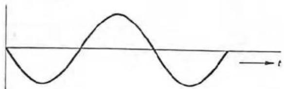
falsch, incorrect
natural_image
Simple sine wave signal diagram with time axis and amplitude label (no text or symbols beyond basic waveform)richtig, correct
b. w.
turn page
tourner s.v.p.
VR 601
To align the erasing current for Metal tapes better a variable resistor 2 kOhm with the reference no. VR 601, part-No. 238 092, has been additional build in up serial no. 20 000.
The VR 601 is located in front of the transistors Q 603 and Q 605. Electrical is the VR 601 with the base resistor R 617 (old value 7,5 kOhm, new one 6,8 kOhm) in series connected. Due to this modification the jumper across D 609 is canceled.
Alignment: Erasing voltage
- operating state, record ON, Metal ON
- Connect AF-millivoltmeter and oscilloscope acros R 653 (erasehead)
- Adjust VR 601 to maximum amplitude (distortion)
- Reduce amplitude until no distortion on the oscilloscope is visible, represents 110 mV + 20 % on R 653.
| "alt" | "neu" | |
| R 464 | 2,2 k | 22,0 k |
| R 465 | 22,0 k | 39,0 k |
| R 466 | 5,6 k | 24,0 k |
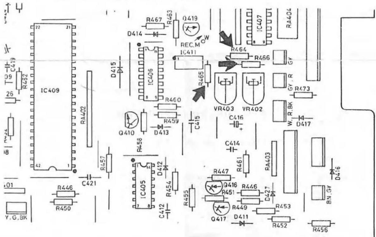
Änderung:
Up to serial no. 15 000 there were 2 different motors ("old" / "new" type) without a marking assembled.
There are only new motors (part no. 271 148) dispatched.
Identification:
Depending on the type of motor used there is following resistor combination on the motor control board (part no. 270 240) to find or to change accordingly.
| Old | new | |
| R 464 | 2,2 k | 22,0 k |
| R 465 | 22,0 k | 39,0 k |
| R 466 | 5,6 k | 24,0 k |
Alteration:
- Special attention has to be paid when the motor gets changed. The above resistors "new" must be in the circuit.
- In case the control motor board (old board) gets changed the "new" board must be modified into the "old" state of the motor-type.
Attention:
A realignment, according to the service manual, is necessary.
The following table provides the original text: "The English text in the source image is not a standard character, but it is not a special character." The OCR result "A" is incorrect because the visual content is not present in the source image.
- Description of functions
- Analog section
- Playback
- Music finder
- Recording
- Fade edit
- Monitor
- Muting, Auto-Space
- Recording level indications
- Device control
- Processor
- Reset
- Inputs
- DLL
- End of tape switch-off
- Outputs
- Capstan motor, reel motor
- Auto-space
- Record standby
- LED display
- Counter
- Remote control
- In Function by
- Transistorentabelle Dolby
- Alignment: Erasing voltage
- Änderung:
- Identification:
- Alteration:
- Attention:
Brand : DUAL
Model : C 844
Category : Cassette tape