CR 1730 - Turntable DUAL - Free user manual and instructions
Find the device manual for free CR 1730 DUAL in PDF.


| Product type | Turntable / Integrated stereo amplifier-tuner |
| Brand | Dual |
| Model | CR 1730 |
| FM tuning range | 87.5 – 108 MHz |
| AM tuning range (MW) | 510 – 1620 kHz |
| AM tuning range (LW) | 150 – 340 kHz |
| FM sensitivity (mono) | 0.8 μV (75 Ω, 26 dB S/N) |
| FM sensitivity (stereo) | 25 μV (75 Ω, 46 dB S/N) |
| AM sensitivity | 30 μV (MW and LW, 6 dB S/N) |
| Music power output | 2 x 75 W (4 Ω), 2 x 50 W (8 Ω) |
| Sinusoidal power output | 2 x 40 W (4 Ω), 2 x 27 W (8 Ω) |
| Frequency response (Phono RIAA) | 20 Hz – 20 kHz ± 1 dB |
| Harmonic distortion (up to 35 W) | < 0.03% (1 kHz) |
| Stereo crosstalk (1 kHz) | > 40 dB |
| Rumble filter | -3 dB at 50 Hz, 12 dB/octave |
| Noise filter | -3 dB at 6.5 kHz, 12 dB/octave |
| Inputs | Aux, Tape 1, Tape 2, Monitor, Phono (1.8 mV / 5 mV) |
| Outputs | 2 pairs of speakers (4-16 Ω), headphones (1/4"), tape, line |
| Station memory | 5 FM/AM presets |
| Frequency display | Fluorescent digital (FM/AM) |
| Power supply | 115 / 230 V (switchable), 50/60 Hz |
| Maximum power consumption | 500 VA |
| Speaker protection | Fault protection relay |
| Maintenance | Clean with a soft, dry cloth; avoid moisture |
| Spare parts | Available (see list in manual) |
Frequently Asked Questions - CR 1730 DUAL
User questions about CR 1730 DUAL
0 question about this device. Answer the ones you know or ask your own.
Ask a new question about this device
Download the instructions for your Turntable in PDF format for free! Find your manual CR 1730 - DUAL and take your electronic device back in hand. On this page are published all the documents necessary for the use of your device. CR 1730 by DUAL.
USER MANUAL CR 1730 DUAL
Download from www.duals Not for commercial use
INHALT
Seite/Page
| Alignment positions CR 1710 |
| Alignment positions CR 1730 |
| Functional description |
| Alignment instructions |
Bloc diagram CR 1710
| Bloc diagram CR 1730 |
| Wiring diagram CR 1710 |
| Wiring diagram CR 1730 |
| IC - bloc diagram |
Printed circuit boards
| Replacement Parts CR 1710 |
| Exploded view CR 1710 |
| Exploded view CR 1730 |
| Replacement Parts CR 1730 |
Tuning (Scale Pointer)
Volumen, Balance, Loudness
Tape 1, Tape 2, Aux (Cinch, DIN)
Volumen, Balance, Loudness
Description of functions for CR 1710 and CR 1730
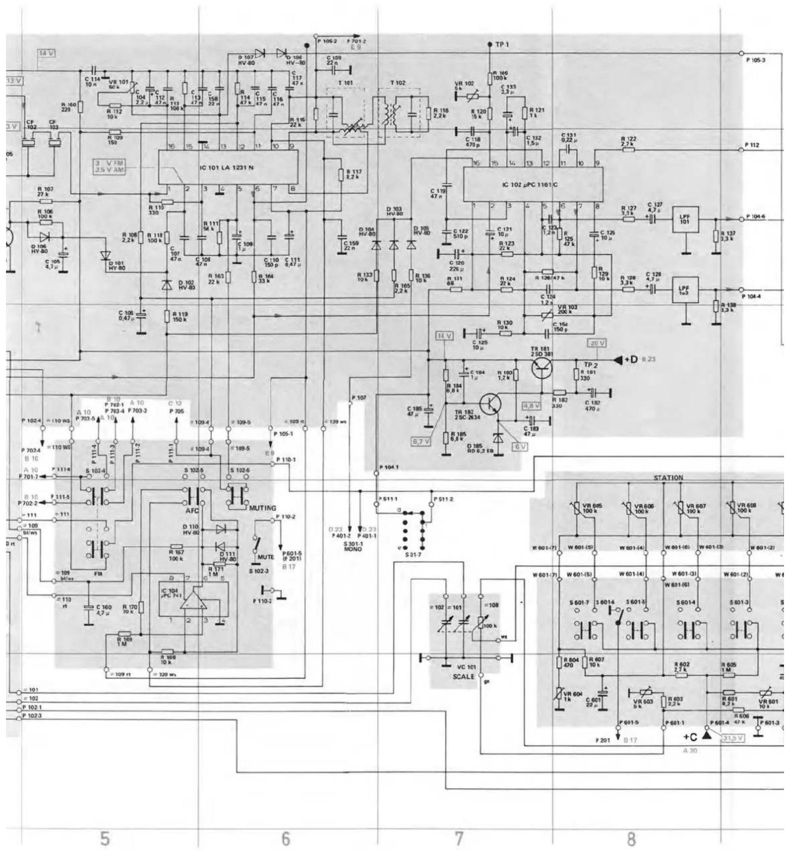
FM tuner section
The receiver has one symmetrical 240/300 Ohm and one asymmetrical 60/75 Ohm antenna input. From the antenna, the RF signal reaches the VHF section and passes through the following stages:
Tunable antenna input circuit
Junction FET RF amplifier
Twofold tuned RF circuit
Mixing stage
Oscillator
Tunable capacitance diode for AFC
First IF stage
FM IF
In the output of the VHF section, the RF signal is converted to an intermediate frequency of 10.7 mHz and routed to the first IF amplifier stage TR 101 via a ceramic filter CF 101. Via the ceramic filter CF 102 and CF 103, from the collector it reaches pin 1 of IC 101, a six-stage IF amplifier and demodulator. Demodulation is carried out in conjunction with coils T 101 and T 102.
Stereo decoder
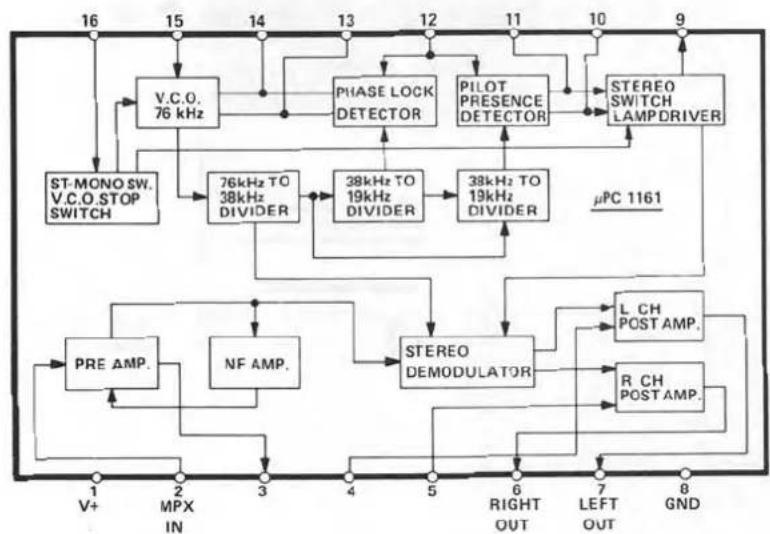
From the AF output pin 6 of IC 101, the signal is routed to pin 2 of the integrated stereo decoder IC 102. In addition to the PLL decoder, the IC comprises an automatic stereo/mono switchover circuit and the driver circuit for the stereo display. The free running frequency of the VCO is set with VR 102 and VR 103 can be used for adjustment to optimum channel separation. The low pass filters LPF 101 and 102 suppress 19 kHz components in the decoded AF signal. The stereo switching threshold is adjusted with VR 101 at an RF input voltage of 8 μV.
AM tuner section
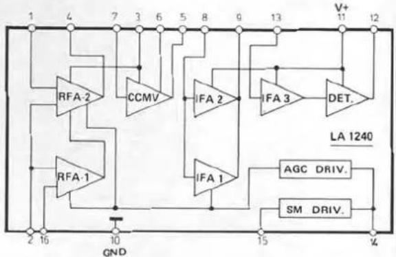
The AM antenna is inductively coupled to the input circuit with a high impedance. S 101 switches primary and secondary circuits of the ferrite antenna and the oscillator circuits. IC 103 comprises the RF amplifier, the mixing stage, the IF amplifier, the rectifier circuit, the automatic gain control and the field strength control. From pin 12 (IC 103), the rectified AF circuit reaches the stereo decoder input pin 2 (IC 102) via R 149, R 146, C 134 and R 145, and then follows the same course as the FMAF signal.
AFC
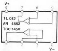
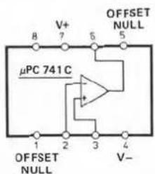
The AF DC voltage from the demodulator IC 102 pin 7 is amplified with IC 104 in order to achieve a large AFC control range. However, in order to prevent excessive extension of the AFC holding range, D 110 and D 111 are contained in the control loop for the purpose of limitation.
FM station memory
The receiver is equipped with a 5 V station memory. The tuning voltage which is routed to the capacitance diodes (D 901, D 902, D 903 and D 904) is adjustable with the controls VR 605, VR 606, VR 607, VR 608 and VR 609. The tuning voltage for MANUAL position is generated with control # 108 which is coupled to the rotary capacitor VC 101. The tuning range can be adjusted with controls VR 601, VR 603 and VR 604, VR 601 and VR 603 are effective in the MANUAL range. The base voltage for the-station memories is adjusted with VR 604.
Only CR 1710
Station direction
The station direction display shows the direction in which the controls of the station memories must be turned in order to achieve the same reception frequency as the one shown on the tuning scale. The circuit operates with the voltage difference between the station memory and the manual scale tuning. If the voltage of the station memory is greater than that of the manual control, the red display lights up. The direction of the arrow shows the direction in which the key switch must be turned. Both LEDs light up when the voltage difference between the two control approaches 0 V (approximately 15 mV). The two voltages are routed to IC 701 which operates as an impedance converter. The differential amplifier IC 702 has a gain of approximately 35 dB. If the voltage difference between the station memory and MANUAL is less than ±15 mV, the transistors TR 701 and TR 702 are reverse biased and a current flows through the diodes D 756, D 701 and D 757. If the differential voltage is ±15 V, TR 701 or TR 702 is forward biased. If the voltage through the Zener diode D 701 is less than the negative bias voltage, the diode is negative biased and either LED D 756 or D 757 lights up.
Signal
The signals for the AM and FM field strength display are routed from pin 15 IC 103 and pin 13 IC 101 to IC 703 via VR 701 or VR 702.
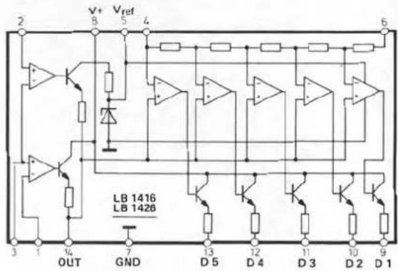
IC 703 drives five LEDs proportionally to the input DC voltage. In AM mode, VR 701 is adjusted at an RF input voltage of 10 mV in such a way that the fifth LED lights up. In the same way, in FM mode VR 702 is adjusted with an input voltage of 200 μV.
Tuning (scale pointer)
The tuning indicator is driven by the DC voltage signal from pin 12 of the FM IF IC 101. This voltage also controls the automatic stereo/mono circuit. The switching threshold for the output signal at pin 12 of IC 101 can be adjusted with VR 101. At the factory, the switching threshold is set to an RF input voltage of 8 V . The DC voltage signal controls transistor TR 703 and switches the small light on the scale pointer.
Muting
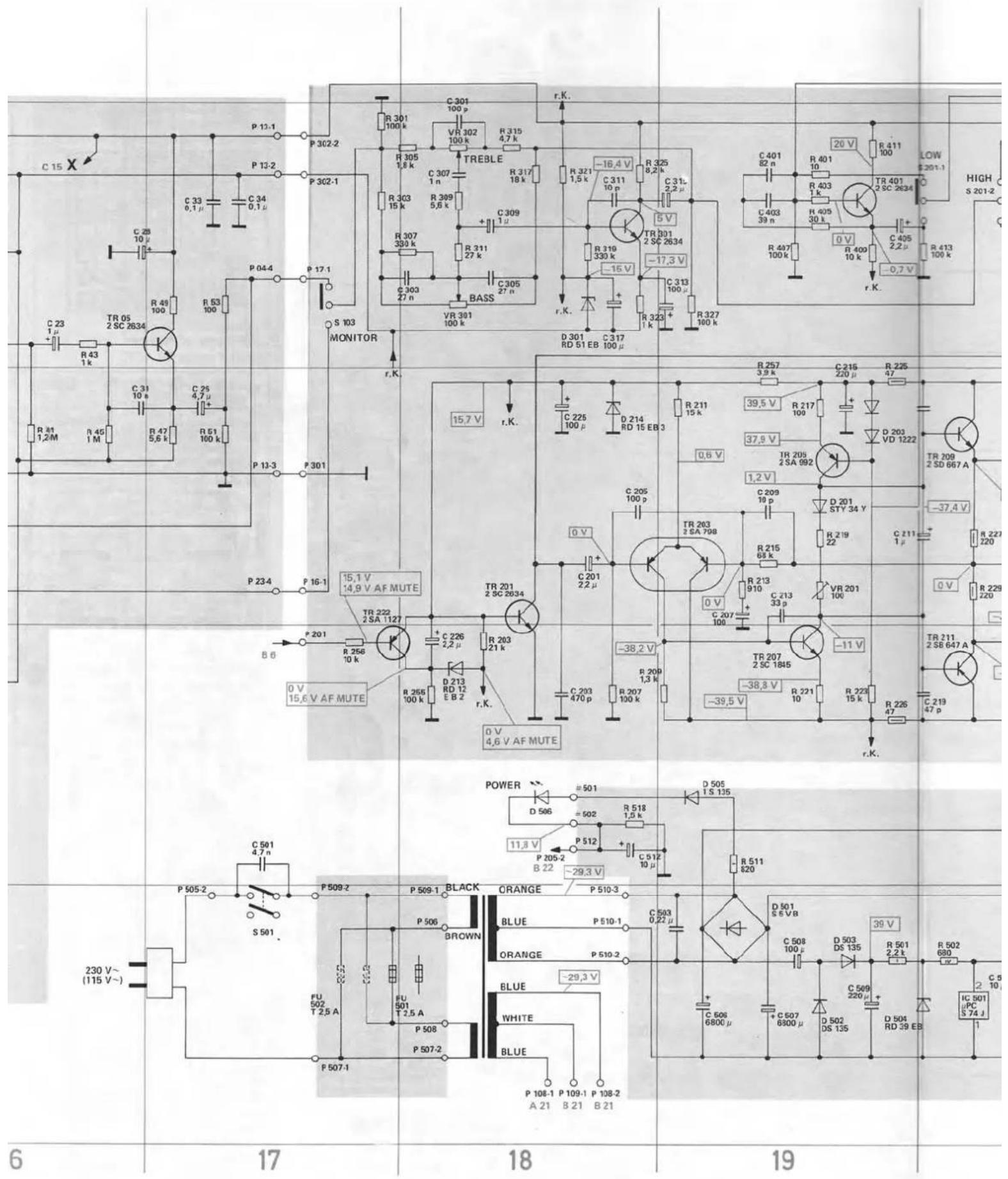
The muting switches S 601-6 (station memory) and S 102-3 (band switch) are mechanically actuated when the band switch and station buttons are operated. The muting signal (active low) reaches the base of TR 218. Via the Zener diode D 205, this switches transistor TR 201 which is parallel to the input of the output stage and which mutes the output stage. In this way, switching noises occurring during operation of the function buttons are suppressed.
Only CR 1730
Signal
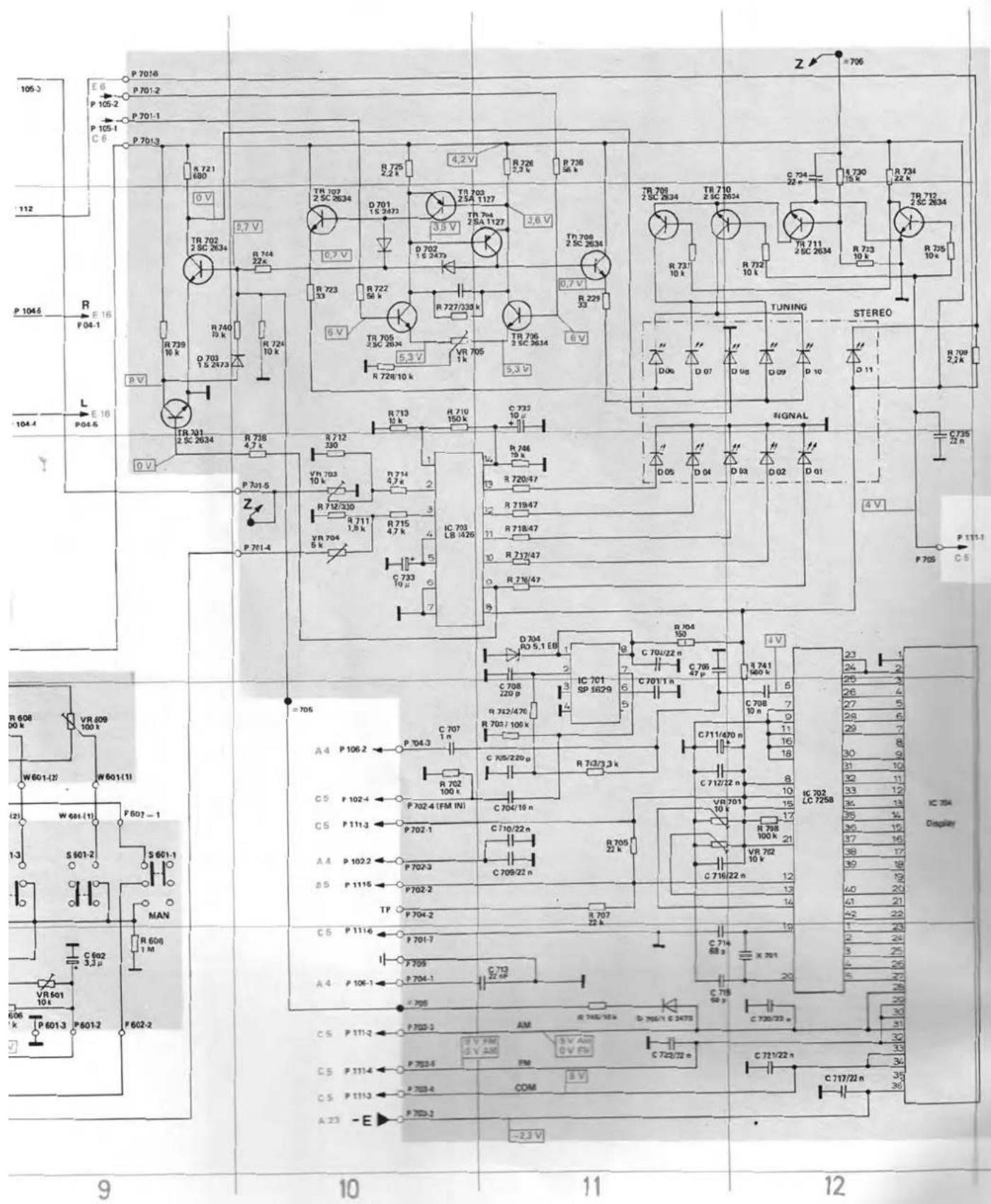
The signals for AM and FM field strength display are routed from pin 15 IC 103 and pin 13 IC 101 to IC 703 via VR 704 or VR 703. IC 703 drives five LEDs proportionally to the input DC voltage.
In AM mode, VR 704 is set at an RF input voltage of 10 mV in such a way that the fifth LED lights up. In the same way, in FM mode VR 703 is adjusted with an input voltage of 200 V.
Tuning
The FM tuning indicator operates with a circuit which consists of 12 transistors (TR 701 - TR 712), four diodes and LEDs. Five pieces of information are gated for indication of the ratio zero passage.
- FM switched
- First field strength LED
- Field strength modulation
- Muting pulse
- Curve of the ratio filter
In AM mode, a high signal is routed to the base of TR 702 via R 745 and D 705, as a result of which the transistor becomes forward biased and LED D 8 (green) can no longer light up.
The modulation signal for the first LED D 701 from pin 9 IC 703 is also routed to the base of TR 701. TR 701 becomes forward biased and prevents TR 702 from also becoming forward biased.
A field strength-dependent signal is routed from pin 13 IC 101 to the base of TR 711. As the voltage increases, TR 711 becomes more conductive and permits TR 709 or TR 710 to switch through.
The muting signal from pin 12 IC 101, which becomes low when the station is exactly tuned, reaches the bases of TR 712 and TR 710. Depending on the amplitude of the muting signal, TR 710 becomes conductive (in the case of tuning by approximately 200 kHz) or TR 709 becomes conductive via TR 712 (in the case of tuning by 100 kHz), resulting in activation of the LEDs D 6 and D 10 or D 7 and D 9.
The ratio voltage is routed to the differential amplifier TR 705 and TR 706 and, via TR 704 or TR 703, TR 708 or TR 707 becomes conductive, as the result of which the operating voltage reaches the LEDs D 9 and D 10 or D 6 and D 7.
Muting
The muting switches S 601-6 (station memory) and S 102-3 (band switch) are mechanically actuated when the band switch and station buttons are operated. The muting signal (active low) reaches the base of TR 222. Via the Zener diode D 213, this switches transistor TR 201 which is located parallel to the input of the output stage and which mutes the output stage. In this way, switching noise occurring during actuation of the function buttons is suppressed.
Display
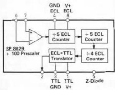
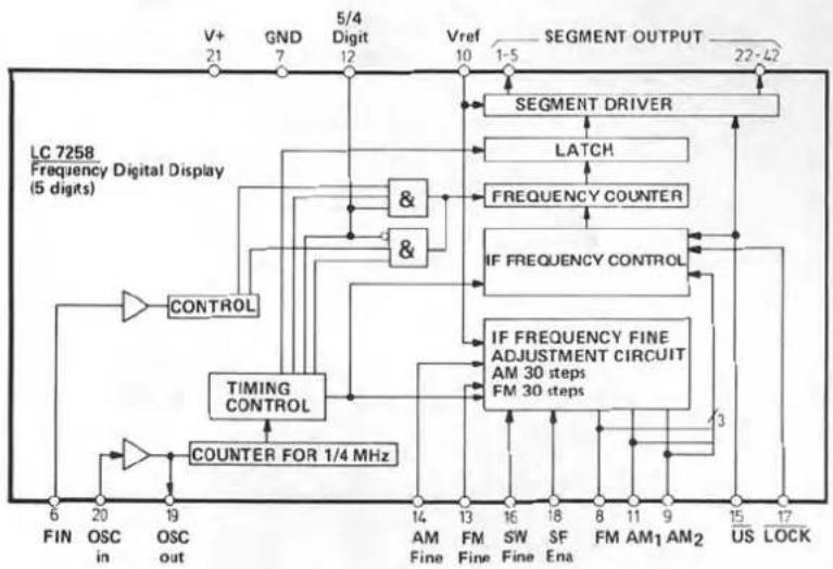
FM frequency display: the FM oscillator frequency is routed to IC 701 via the isolating amplifier in the VHF section TR 904. IC 701 is a single edge ECL predivider with a fixed division ratio of 100. At the output pin 2, the square-wave signal is applied which corresponds to the TTL level and which is routed to IC 702 which, in its turn, drives the fluorescent display during static operation. The frequency display in the FM range can be varied with the control VR 702.
AM frequency display: via the isolating amplifier TR 101, the AM oscillator signal (long wave-medium wave) reaches the input of IC 702. The AM frequency display can be varied with control VR 701.
CR 1710: AF section
Phono (cinch, DIN)
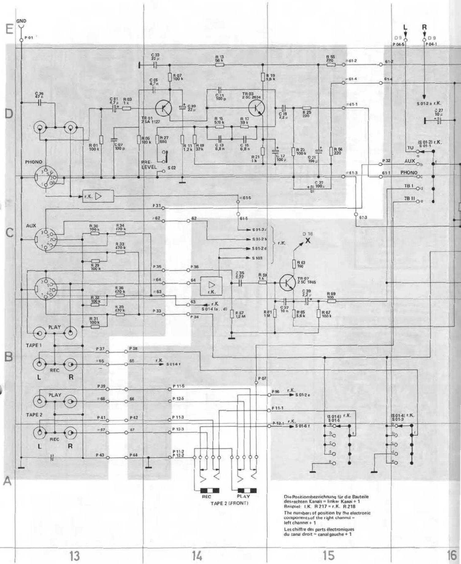
The two-stage phono equalizer preamplifier comprises noise-free transistors. The input sensitivity is switched over with switch SW 02. The input sensitivity for nominal output power is 1.8 mV and 5 mV at 1 kHz. The equalization is carried out in the negative feedback branch with 3180, 318 and 75 μs corresponding to the recording characteristic equalization. The components determining the frequency are R 15, R 17, C 13 and C 15 in the left channel and R 16, R 18, C 14 and C 16 in the right channel. The gain is approximately 41 dB at 1 kHz at the 1.8 mV switch setting.
Tape 1 and Tape 2 (cinch, DIN)
In order to guarantee an input impedance of 470 kOhm, there is an impedance converter (TR 05) after the input selector switches S 01-1 to S 01-5.
Tone controls
The tone controls are located in the negative feedback branch of the transistors TR 301 and TR 302. VR 301 serves to adjust the treble frequencies and VR 302 serves to adjust the base frequencies.
Mono
The left and right channels are merged with the mono switch (S 301-1). A level surge due to the addition is prevented with resistors R 331 and R 332. Via R 135 and D 105, operating voltage is applied to pin 16 of IC 102 and, as a result of this, the stereo decoder is switched to MOND.
Volume, balance, loudness
The volume control VR 201 is located on the front of the output amplifier. Equally, the balance control VR 202 is located on the front of the output amplifier board. It is designed such that only one channel is active when the control is set to extreme right or left-hand position. At a volume level of -40 dB, the loudness circuit causes boosting of +12 dB at 40 Hz and +6 dB at 15 kHz.
Output stage
The transistors TR 201 and TR 202 perform the muting function (see muting). The output amplifier is a non-ferrous complementary output stage with an AF output having neither DC voltage nor electrolytic capacitors. Via the deferential amplifier TR 203 and TR 204, the AF signal is routed to the transistors TR 205 and TR 206. The zero signal current is stabilized via TR 207 and TR 208. The complementary driver transistors (TR 209, TR 210, TR 211 and TR 212) amplify the AF signal and drive the power output transistors TR 213, TR 214, TR 215 and TR 216, which are also complementary. The output signal is routed to the loudspeaker connections via the fuse FU 201 and the switching contacts of the headphone socket. The loudspeaker outputs are deactivated by connecting a plug to the headphone socket.
Power supply unit
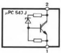
The power supply unit is designed for supply voltages of 230 V and 115 V (AC voltage). In order to convert the voltage, the fuses (FU 501 and FU 502) on the power supply board must be changed in accordance with the data printed on the board. The secondary side of the mains transformer has two windings: one main winding for generation of the operating voltage for the output amplifier, the preamplifier, the impedance converter, the equalizer preamplifier, for generation of the tuning voltage and operating voltages of the RF section and a smaller windings for the lamps for illumination of the tuning scale. IC 501 is a special integrated circuit which compensates for temperature drifts.
CR 1730: AF section
Phono (cinch, DIN)
Refer to the details on the phono input of the CR 1710.
Tape 1, tape 2, aux (cinch, DIN)
In order to guarantee an input impedance of 470 kOhm, an impedance converter (TR 05) is located after the input selector switch (S 01-1 to S 01-6). In addition, tape 1 has an impedance converter (TR 07) for the monitor function. When the front sockets of tape 2 are occupied, the sockets for tape 2 on the rear are deactivated.
Monitor
The signal from tape 1 can be directly switched through with the monitor switch S 103. An impedance converter (TR 07) ensures correct matching.
Tone controls
The tone controls are located in the negative feedback branch of TR 301 and TR 302. VR 301 serves to adjust the treble frequencies and VR 302 serves to adjust the base frequencies.
High and low filters
The filters have a drop of 12 dB per octave, response frequency of the low filter (S 201-1) at 50 Hz and of the high filter (S 201-2) at 6.5 kHz.
Mono
The left and right channels are merged by the mono switch (S 201-3). A level surge caused by the addition is prevented with resistors R 433 and R 434. Via R 135 and D 105, operation voltage is applied to pin 16 of IC 102 and the stereo decoder switches to MONO.
Volume, balance, loudness
The volume control VR 401 is located on the front of the output amplifier. Equally, the balance control VR 402 is located on the front of the output amplifier board. It is designed such that only one channel is active when the control is set to the extreme right or left-hand position. At a loudness level of -40 dB, the loudness circuit causes boosting of +12 dB at 50 Hz and +6 dB at 10 kHz.
Output stage
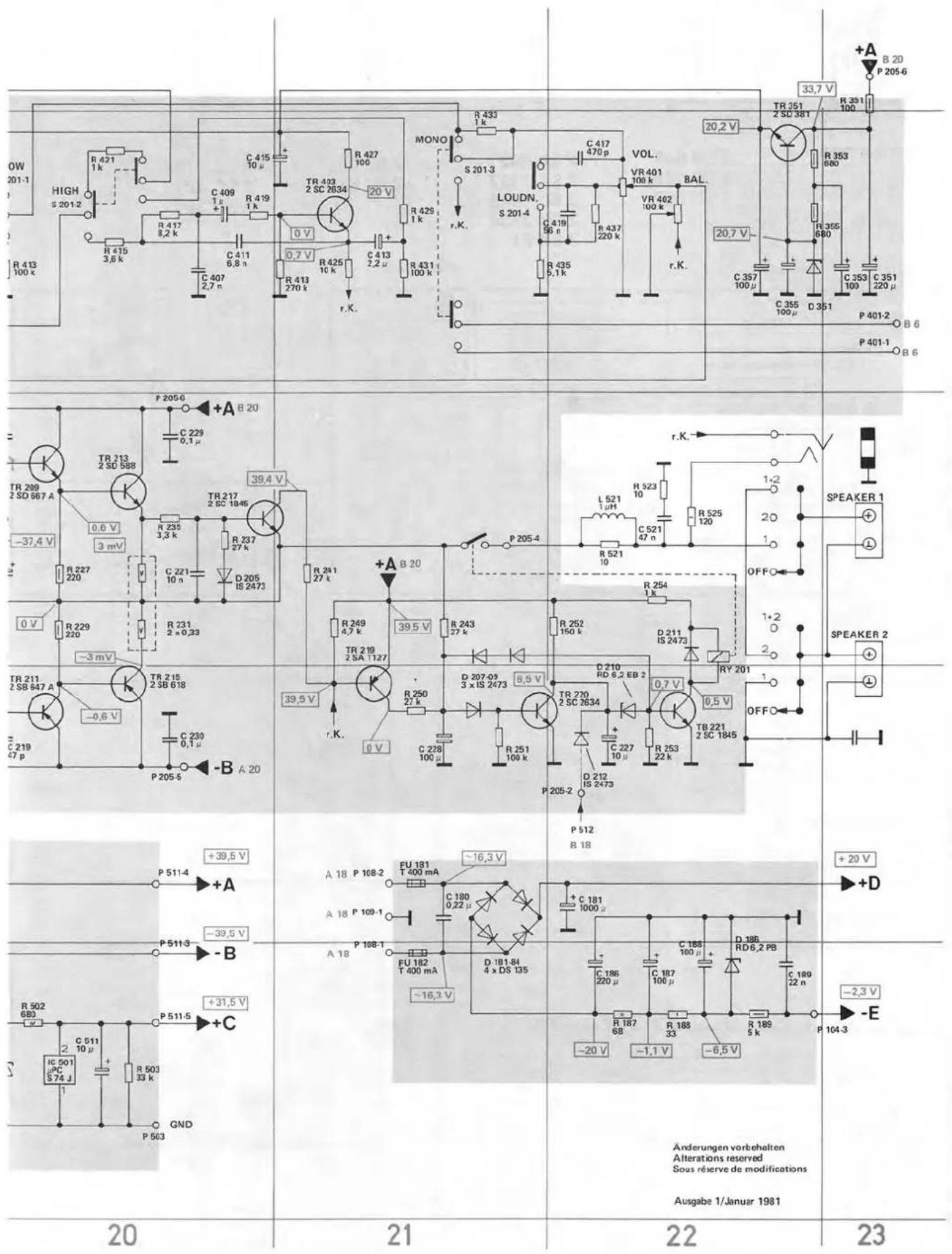
The transistors TR 201 and TR 202 perform the muting function (see muting). The output amplifier is a non-ferrous complementary output stage having an AF output without DC voltage and without electrolytic capacitors. Via the differential amplifier DR 203, the AF signal is routed to the transistor TR 207. The zero signal current is stabilized via TR 205 and adjusted with VR 201. The complementary driver transistors (TR 209, TR 211) amplify the AF signal and drive the power output transistors TR 213 and TR 215, which are also complementary. The output signal is routed to the loudspeaker output and the headphone connection via the switching contacts of the relay and the "speaker" selector switch S 502. If the "speaker" selector switch is in position "1 and 2", the connected pairs of speakers are series connected in each channel.
Speaker protection circuit
The task of the protective circuit is to prevent a voltage from reaching the speaker output should a defect occur. This is achieved by TR 221 becoming reverse biased and relay RY 201 becoming de-energized, as a result of which the switching contacts interrupt the AF path. Under normal operating conditions, TR 221 in the protective circuit is the only transistor which becomes conductive.
If, in the event of a defect, a positive or negative DC voltage is applied to the loudspeaker output in the area of the power transistors TR 213—TR 216, D 207 detects the positive DC voltage. TR 220 becomes conductive, the base of TR 222 becomes low and thus TR 222 becomes negative biased. In the case of a negative DC voltage, the diodes D 208 and D 209 become conductive, TR 221 becomes negative biased and the relay is de-energized.
If there is a short-circuit at the speaker output, the voltage drop over R 231 (TR 230) increases, transistor TR 217 becomes conductive, the base voltage at TR 219 drops and thus this transistor becomes forward biased. Via D 207, the positive DC voltage is switched through TR 220, TR 221 becomes negative biased and the relay is de-energized.
Switch-on delay: the relay is not energized until both speaker outputs reliably conduct 0 V DC voltage.
Power supply unit
The power supply is designed for supply voltages of 230 V and 115 V (AC voltage). To convert the voltage, the fuses (FU 501 and FU 502) must be changed on the power supply board in accordance with the data printed on the board. The secondary side of the mains transformer has two windings: one main winding to generate the operating voltage for the output amplifier, the preamplifier, the impedance converter, the filter circuit and the equalizer preamplifier. The other winding is for the RF section and the bias voltage of the fluorescent display. The tuning voltage of the capacitance diodes is also generated by the main winding and rectified via diodes D 502 and D 503. The FM tuning voltage is stabilized with IC 502, which compensates for temperature drifts.
Adjustment instructions for CR 1710 / CR 1730
| Signal source | Signal source adjustment | Unit adjustment | Display unit connection | Adjustment position | Adjustment |
| AM-IF | |||||
| Loosely couple a wob-bulator to the ferrite antenna | 455 kHz | Transmitter-free frequency | Oscilloscope to TP 3 and P 102, pin 2 (±) | T 103, T 106 | Maximum and symmetry |
| MW-RF, signal indication, LW-RF | |||||
| AM signal generator via DIN dummy antenna to antenna input | 1 kHz, 30 % modulated | Oscilloscope and AF voltmeter via 4 Ohm resistance to loud-speaker output | |||
| 510 kHz 50 - 100 μV | Bottom end | T 105 | Maximum | ||
| 1650 kHz 50 - 100 μV | Top end | TC 104 | Maximum | ||
| Repeat adjustment several times | |||||
| 600 kHz 10 - 50 μV | 600 kHz | Ferrite antenna MW | Maximum | ||
| 1400 kHz 10 - 50 μV | 1400 kHz | TC 102 | Maximum | ||
| Repeat adjustment several times | |||||
| 1000 kHz 10 mV | 1000 kHz | CR 1710 CR 1730 VR 701 VR 703 | Fifth LED must light up | ||
| 145 kHz 50 - 100 μV | Bottom end | T 104 | Maximum | ||
| 350 kHz 50 - 100 μV | Top end | TC 103 | Maximum | ||
| Repeat adjustment several times | |||||
| 160 kHz 10 - 50 μV | 160 kHz | Ferrite antenna LW | Maximum | ||
| 320 kHz 10 - 50 μV | 320 kHz | TC 101 | Maximum | ||
| FM-IF | Repeat adjustment several times | ||||
| Wobbulator to IF and GND | Aprox. 10.7 MHz | AFC from transmitter-free frequency | Oscilloscope to TP 2 and P 102, pin 2 (±) | T 101, T 102 | S-curve to maximum and symmetry |
| FM-RF | |||||
| FM signal generator to 75/60 Ohm antenna input | ±40 kHz Dev. Modulated 1 kHz | AFC from FM-Station man. | Oscilloscope and AF voltmeter via 4 Ohm load resistance to loudspeaker output | ||
| 87.5 MHz 1 - 2 μV | Bottom end | VR 603 | Until signal received | ||
| 108.5 MHz 1 - 2 μV | Top end | VR 601 | Until signal received | ||
| FM Station 1 | Repeat adjustment several times | ||||
| 87.5 MHz 1 - 2 μV | Bottom end | VR 604 | Until signal received | ||
| >108 MHz 1 - 2 μV | Top end | Check for signal reception | |||
| AFC, harmonic distortion | Repeat adjustment several times | ||||
| FM signal generator to 75/60 Ohm antenna input | Approx. 98 MHz without signal | FM-Station man. | Oscilloscope and AF voltmeter via 4 Ohm load resistance to loudspeaker output DC voltmeter to P 105, pins 1 + 2 | T 101 | 0 V ±50 mV (DC-Voltm.) |
| Approx. 98 MHz 1 mV | To signal | T 102 | Minimum harmonic distortion | ||
| FM, MPX, VCO, Stereo channel separation | Repeat adjustment several times | ||||
| Stereo modulator via FM signal generator to 60/75 Ohm antenna input | Oscilloscope and AF voltmeter via 4 Ohm load resistance to loudspeaker output, frequency meter to TP 1 and P 104, pin 5 (±) | ||||
| Approx. 98 MHz without signal | FM-Station man. | VR 102 | 76 kHz ± 0.05 % | ||
| Approx. 98 MHz 1 mV only left channel | FM-Station man. to signal | VR 103 | Maximum channel separation | ||
| Approx. 98 MHz 1 mV only right channel | FM-Station man. | Check channel separation for maximum | |||
| Signal display FM | Repeat adjustment several times | ||||
| FM signal generator to 60/75 Ohm antenna input | Approx. 98 MHz 200 μV | FM-Station man. to signal | Oscilloscope and AF voltmeter via 4 Ohm load resistance to loudspeaker output | CR 1710 CR 1730 VR 702 VR 703 | Fifth LED must light up |
| Scale pointer, Stereo trigger CR 1710 Repeat adjustment several times | |||||
| FM signal generator to 75/60 Ohm antenna input | Approx. 98 MHz 8 μV modulated only right channel or left channel | FM station man. to signal | Oscilloscope and AF voltmeter via 4 Ohm load resistance to loudspeaker output | VR 101 | Lamp must light up |
| Stereo trigger CR 1730 Repeat adjustment several times | |||||
| FM signal generator to 75/60 Ohm antenna input | Approx. 98 MHz 8 μV modulated only right channel or left channel | FM station man. to signal | Oscilloscope and AF voltmeter via 4 Ohm load resistance to loudspeaker output | VR 101 | To stereo switchover |
| Station Direction CR 1710 | |||||
| At P 701, short-circuit pins 4 + 5 | DC voltmeter to P 511, pin 6 and R 729 | VR 703 | To 0 V ± 10 mV | ||
| Tuning CR 1730 | |||||
| FM signal generator to 75/60 Ohm antenna input | 98 MHz 1 - 2 μV | FM station man. to signal | DC voltmeter via R 727 | VR 705 | To 0 V ± 10 mV |
| Display CR 1730, FM frequency display | |||||
| FM signal generator to 60/75 Ohm antenna input | 98,000 MHz 1 mV | FM station man. to signal | Short-circuit pin 2 of P 702 with pin 7 of P 701 | VR 702 | Display to 98.000 MHz, 100 kHz display must not flicker |
| AM frequency display | |||||
| AM signal generator via DIN dummy antenna to antenna input | 1000 kHz 1 mV | To signal | VR 701 | Display to 1000 kHz | |
| AF, Zero signal current CR 1730 | |||||
| Selection: Aux Volume : Minimum | DC voltmeter to P 203, P 1 + 4 left channel, DC voltmeter to P 204, pins 1 + 4 right channel | VR 201VR 202 | Approx. 7 mAApprox. 7 mA | ||
Mémoire de stations FM
Tuning (Scale Pointer)
Volume, Balance, Loudness
Tape 1, Tape 2, Aux (Cinch, DIN)
Volume, Balance, Loudness
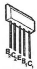
2 SA 798
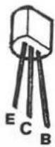
2 SB 647
2 SC 1675
2 SD 667
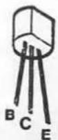
2 SA 992
2 SA 1127
2 SC 1845
2 SC 2634
2 SK 61
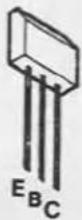
2 SC 461
2 SC 535
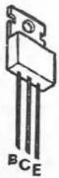
2 SA 769
2 SC 1827
2 SD 381
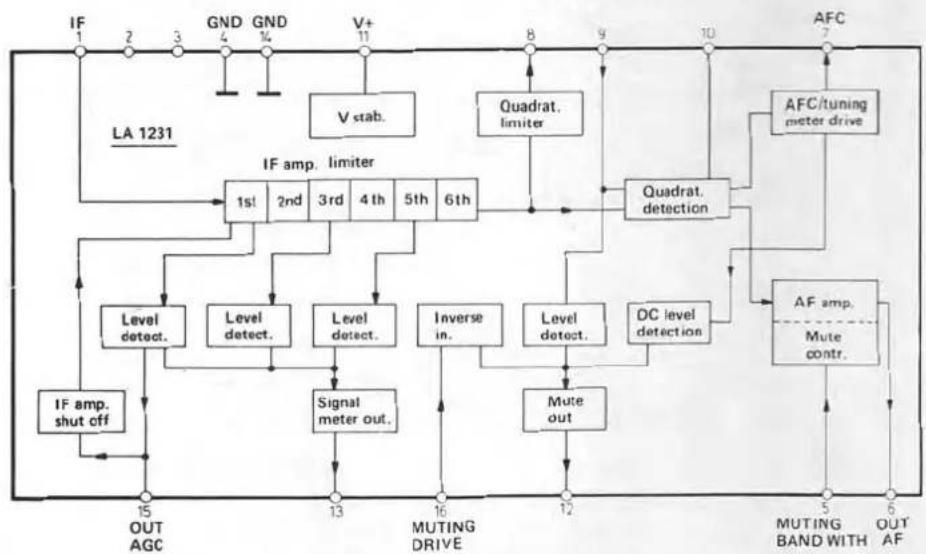
flowchart
graph TD
    A["IF 1"] --> B["LA 1231"]
    B --> C["IF amp. limiter"]
    C --> D["1st"]
    D --> E["2nd"]
    E --> F["3rd"]
    F --> G["4th"]
    G --> H["5th"]
    H --> I["6th"]
    I --> J["Quadrat. limiter"]
    J --> K["Quadrat. detection"]
    K --> L["AFC/ tuning meter drive"]
    L --> M["AFC"]
    M --> N["Mute contr."]
    N --> O["AF amp. Mute"]
    O --> P["MUTING BAND WITH"]
    P --> Q["OUT AF"]
    Q --> R["MUTING DRIVE"]
    R --> S["Signal meter out."]
    S --> T["Level detect."]
    T --> U["Level detect."]
    U --> V["Level detect."]
    V --> W["Inverse in."]
    W --> X["Level detect."]
    X --> Y["Mute out"]
    Y --> Z["OUT AGC"]
    Z --> AA["IF amp. shut off"]
    AA --> AB["IF amp. shut off"]
    AB --> AC["1st"]
    AC --> AD["2nd"]
    AD --> AE["3rd"]
    AE --> AF["4th"]
    AF --> AG["5th"]
    AG --> AH["6th"]
    AH --> AI["Quadrat. Detection"]
    AI --> AJ["AFC/ tuning meter drive"]
    AJ --> AK["MUTING BAND WITH"]
    AK --> AL["OUT AF"]
flowchart
graph TD
    A["SP 8629 + 100 Prescaler"] --> B["÷5 ECL Counter"]
    B --> C["÷5 ECL Counter"]
    C --> D["÷4 ECL Counter"]
    D --> E["ECL+TTL Translator"]
    E --> F["TTL GND"]
    E --> G["TTL V+"]
    F --> H["Z-Diode"]
    G --> H
    I["GND ECL 4"] --> J["÷5 ECL Counter"]
    K["V+ ECL 8"] --> L["÷5 ECL Counter"]
    M["2"] --> N["ECL+TTL Translator"]
    O["3"] --> P["TTL GND"]
    Q["1"] --> R["TTL V+"]
flowchart
graph TD
    A["FIN"] --> B["OSC in"]
    B --> C["OSC out"]
    C --> D["Timing CONTROL"]
    D --> E["COUNTER FOR 1/4 MHz"]
    E --> F["AM Fine"]
    E --> G["FM Fine"]
    E --> H["SW Fine"]
    E --> I["SF Ena"]
    E --> J["FM AM1 AM2"]
    E --> K["US LOCK"]
    L["V+"] --> M["21"]
    N["GND"] --> O["7"]
    P["5/4 Digit"] --> Q["12"]
    R["Vref"] --> S["10"]
    T["SEGMENT OUTPUT"] --> U["22-42"]
    V["SEGMENT DRIVER"] --> W["LATCH"]
    X["FREQUENCY COUNTER"] --> Y["IF FREQUENCY CONTROL"]
    Z["IF FREQUENCY FINE ADJUSTMENT CIRCUIT AM 30 steps FM 30 steps"] --> AA["3"]
    AB["CONTROL"] --> AC["&"]
    AD["&"] --> AE["&"]
    AF["SEGMENT DRIVER"] --> AG["LATCH"]
    AH["FREQUENCY COUNTER"] --> AI["IF FREQUENCY CONTROL"]
    AJ["IF FREQUENCY FINE ADJUSTMENT CIRCUIT AM 30 steps FM 30 steps"] --> AK["3"]
flowchart
graph TD
    A["16"] --> B["V.C.O. 76 kHz"]
    B --> C["PHASE LOCK DETECTOR"]
    C --> D["PILOT PRESENCE DETECTOR"]
    D --> E["STEREO SWITCH LAMPDRIVER"]
    E --> F["μPC 1161"]
    F --> G["PRE AMP."]
    F --> H["NF AMP."]
    G --> I["MPX IN"]
    H --> J["38kHz TO 19kHz DIVIDER"]
    J --> K["STEREO DEMODULATOR"]
    K --> L["L CH POST AMP."]
    K --> M["R CH POST AMP."]
    L --> N["RIGHT OUT"]
    M --> O["LEFT OUT"]
    N --> P["GND"]
    O --> Q["GND"]
    B --> R["ST-MONO SW. V.C.O.STOP SWITCH"]
    R --> S["76kHz TO 38kHz DIVIDER"]
    S --> T["38kHz TO 19kHz DIVIDER"]
    T --> U["STEREO DEMODULATOR"]
    U --> V["L CH POST AMP."]
    U --> W["R CH POST AMP."]
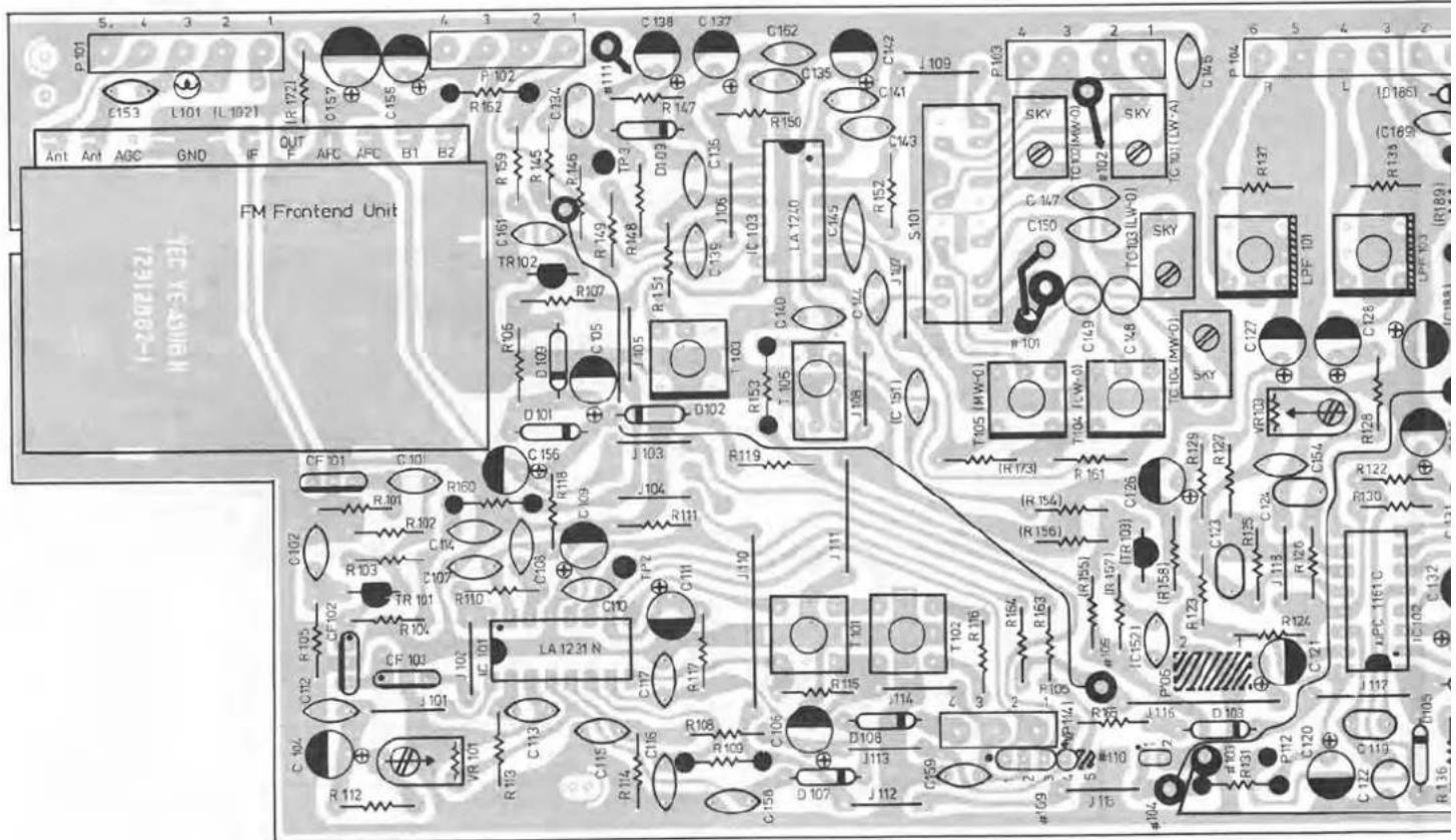
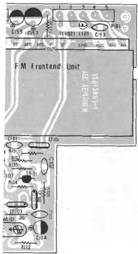
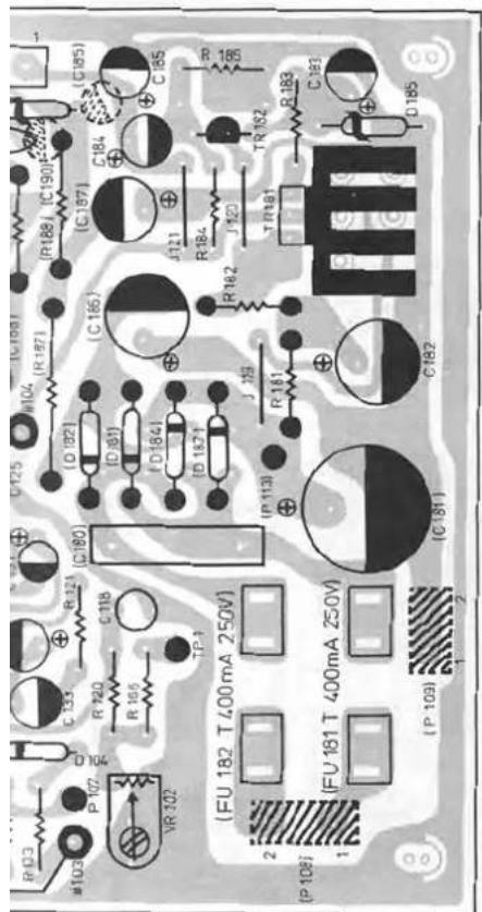
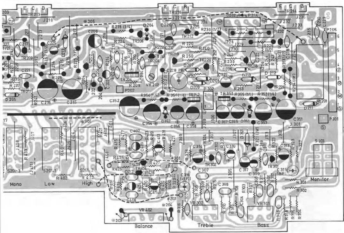
Tunerplatte / Tuner PWB / Plaquette HF L
Filterplatte CR 1730 /
Filter plate CR 1730 /
Plaque de Filtre CR 1730
B
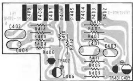
Monitorplatte CR 1730 /
Monitor plate CR 1730 /
Plaque monitor CR 1730
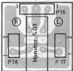
L
Volumeplatte CR 1730 /
Volume plate CR 1730 /
Plaque de volume CR 1730
B

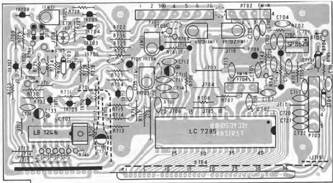
Displayplatte CR 1730 / Display board CR 1730 / Plaque d'image CR 1730
B
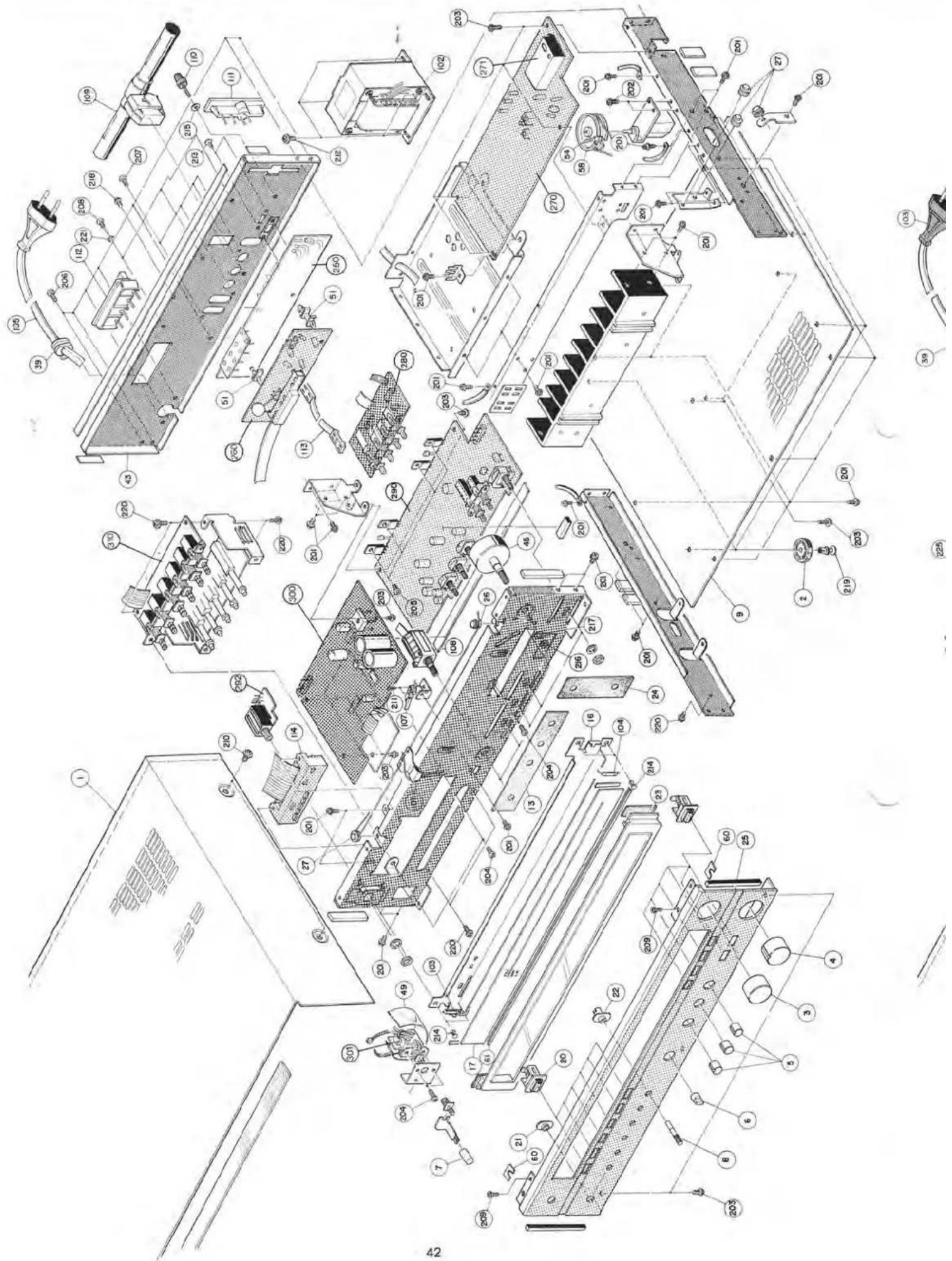
| Pos. | Art.-Nr.Part.No.Référ. | StckQty.ndp. | Bezeichnung | Description | Designation | ||
| 1 | 266 885 | 1 | Abdeckblech | Top cover plate | Tôle de recouvrement | ||
| 2 | 266 886 | 4 | Fuß | Base | Socle | ||
| 3 | 266 887 | 1 | Tuningknopf | Tuning knob | Bouton (Tuning) | ||
| 4 | 266 888 | 1 | Volumeknopf | Volume knob | Bouton (Volume) | ||
| 5 | 266 889 | 3 | Klangstellerknopf | Tone control knob | Bouton (Bass, Treble, Balance) | ||
| 6 | 266 890 | 1 | Selectionknopf | Selection knob | Bouton (Selection) | ||
| 7 | 266 891 | 1 | Powerknopf | Power knob | Bouton (Power) | ||
| 8 | 266 892 | 1 | Einstellschlüssel | Preset Wrench | Clef de réglage | ||
| 9 | 267 095 | 1 | Bodenblech | Bottom cover plate | Tôle de fond | ||
| 13 | 267 096 | 1 | Abdeckfilz | Felt | Feutre | ||
| 16 | 267 097 | 1 | Skalenblech | Scale Decoration plate | Tôle de Cadran | ||
| 17 | 266 895 | 1 | Skala | Scale | Cadran | ||
| 20 | 266 963 | 1 | Taste | Button | Touche | ||
| 21 | 266 897 | 1 | Führungsbuchse | Guide sleeve | Douille de quidage | ||
| 22 | 266 898 | 1 | Klemmbuchse | Clamp bush | Douille de serrage | ||
| 23 | 267 122 | 1 | Skalenfenster | Window | Fenêtre | ||
| 24 | 267 098 | 1 | Filz | Felt | Feutre | ||
| 25 | 266 974 | 1 | Frontblende kpl. | Front trim-plate | Panneau frontal | ||
| 26 | 266 883 | 1 | Seilrolle | Dial roll | Poulie | ||
| 27 | 267 099 | 4 | Seilrolle | Dial roll | Poulie | ||
| 36 | 267 100 | 1 | Kabelhalter | Holder | Support | ||
| 39 | 237 548 | 1 | Zugentlastung | Cable inlet | Passe-câble | ||
| 43 | 267 121 | 1 | Rückwand | Rear panel | Paroi arrière | ||
| 45 | 266 918 | 1 | Schwungmasse | Tuning | Volant | ||
| 49 | 267 131 | 1 | Isolierung | Insulation | Isolation | ||
| 51 | 267 102 | 1 | Plattenhalter | PWB Holder | Serrage | ||
| 54 | 266 893 | 1 | Zugfeder | Tension spring | Resort de traction | ||
| 58 | 266 884 | 1 | Drehkorolle | Variable capacitor roll | Roulleau de condensateur variable | ||
| 60 | 267 128 | 2 | Unterlagstück | Substratum | Couche inférieure | ||
| 101 | 267 103 | 1 | Zeiger kpl. | Pointer | Aiquille | ||
| 102 | 266 977 | 1 | Netztrafo kpl. | Transformer cpl. | Transformateur | ||
| 103 | 266 903 | 1 | Skalenlampe links | Lamp left | Lampe | ||
| 104 | 266 904 | 1 | Skalenlampe rechts | Lamp right | Lampe | ||
| 105 | 243 750 | 1 | Netzkabel | Mains lead | Câble secteur | ||
| 107 | 267 104 | 1 | Stummschalter | Muting switch | Interrupteur silencieux | ||
| 108 | 267 105 | 1 | Selectionschalter | Selection switch | Selecteur d'entrée | ||
| 109 | 266 912 | 1 | Ferritantenne kpl. | Antenne ferrite, completa | Ferrite rod antenna cpl. | ||
| 110 | 266 913 | 1 | Erdanschlußschraube | Ground terminal | Prise de terre | ||
| 111 | 266 914 | 1 | Antennenbuchse | Antenna bush | Prise d'antenne | ||
| 112 | 266 915 | 1 | Lautsprecheranschlußklemme | Loudspeaker jack | Réglette de bornes | ||
| 113 | 267 127 | 1 | Schalterverbindung | Remote Wire SWR | Connexion de l'interrupteur | ||
| 114 | 266 976 | 1 | LED-Einheit kpl. | LED panel compl. | Plaque de diodes lumineuses compl' | ||
| 201 | 227 487 | 38 | Sechskantblechschraube | Hexagon screw | Vis Parker hexagonale | ||
| 202 | 218 055 | 4 | Linsenblechschraube | Self tapping screw | Vis Parker à tête bombée | ||
| 203 | 218 055 | 16 | Linsenblechschraube | Self tapping screw | Vis Parker à tête bombée | ||
| 204 | 210 475 | 13 | Zyinderschraube | Machine screw | Vis à tête cylindrique | ||
| 205 | 210 487 | 4 | Zyinderschraube | Machine screw | Vis à tête cylindrique | ||
| 208 | 267 106 | 1 | Spezialschraube | Special screw | Vis à tête spéciale | ||
| 209 | 210 387 | 2 | Senkschraube | Sunk screw | Vis à tête fraisée | ||
| 210 | 267 107 | 4 | Spezialschraube | Special screw | Vis à tête spéciale | ||
| 211 | 267 108 | 2 | Linsenschraube | Machine screw | Vis à tête bombée | ||
| 212 | 267 109 | 4 | Spezialschraube | Special screw | Vis à tête spéciale | ||
| 213 | 237 823 | 2 | Zyinderschraube | Machine screw | Vis à tête cylindrique | ||
| 216 | 267 129 | 1 | Sechskantmutter | Hexagonal nut | Ecron à six pans | ||
| 217 | 226 295 | 1 | Scheibe | Washer | Rondelle | ||
| 218 | 265 752 | 1 | Bedienungsanleitung | Service Manual | Instructions de service | ||
| 220 | 267 851 | 1 | Verpackungskarton kpl. | Shipping carton | Carton d'emballage | ||
| Eingangsplatte | Input Terminal PWB | Circuit d'entrée | |||||
| 250 | 266 989 | 1 | Eingangsplatte kpl. | Input Terminal PWB compl. | Circuit d'entrée comp. | ||
| TR | 1 | 266 947 | 2 | 2 SA 1127 S | 2 SA 1127 S | ||
| TR | 2 | 266 947 | 2 | 2 SA 1127 S | 2 SA 1127 S | ||
| TR | 3 | 266 938 | 2 | 2 SC 2634 S | 2 SC 2634 S | ||
| TR | 4 | 266 938 | 2 | 2 SC 2634 S | 2 SC 2634 S | ||
| 260 | 266 990 | 1 | DIN-Buchse | DIN Jack | Prise DIN à | ||
| Pos. | Art.-Nr.Part.No.Réfer. | StckQty.ndp. | Bezeichnung | Description | Designation | ||||
| D 108 | 266 959 | 9 | HV 80 | HV 80 | HV 80 | ||||
| D 109 | 266 959 | 9 | HV 80 | HV 80 | HV 80 | ||||
| D 185 | 266 922 | 1 | RD-6,2 EB | RD-6.2 EB | RD-6,2 EB | ||||
| TR 101 | 266 937 | 1 | 2 SC 2634 M | 2 SC 2634 M | 2 SC 2634 M | ||||
| TR 102 | 266 938 | 2 | 2 SC 2634 S | 2 SC 2634 S | 2 SC 2634 S | ||||
| TR 181 | 266 939 | 2 | 2 SD 381 L | 2 SD 381 L | 2 SD 381 L | ||||
| TR 182 | 266 938 | 1 | 2 SC 2634 S | 2 SC 2634 S | 2 SC 2634 S | ||||
| IC 101 | 266 923 | 1 | LA 1231 N | LA 1231 N | LA11231 N | ||||
| IC 102 | 266 924 | 1 | μPC-1161 C | μPC-1161 C | μPC-1161 C | ||||
| IC 103 | 266 925 | 1 | LA 1240 | LA 1240 | LA 1240 | ||||
| LF 101 | 266 928 | 2 | Filter | Filter | Filtre | ||||
| LF 102 | 266 928 | 2 | Filter | Filter | Filtre | ||||
| VR 101 | 266 969 | 1 | Steller 50 kΩ | Variable Resistor 50 kΩ | Régulateur 50 kΩ | ||||
| VR 102 | 266 970 | 1 | Steller 5 kΩ | Variable Resistor 5 kΩ | Régulateur 5 kΩ | ||||
| VR 103 | 266 971 | 1 | Steller 200 kΩ | Variable Resistor 200 kΩ | Régulateur 200 kΩ | ||||
| VC 101 | 266 940 | 1 | Drehkondensator | Variable capacitor | Condensateur variable | ||||
| TC 101 | 266 966 | 1 | Trimmer 15 pF | Trimmer 15 pF | Trimmer 15 pF | ||||
| TC 102 | 266 967 | 2 | Trimmer 10 pF | Trimmer 10 pF | Trimmer 10 pF | ||||
| TC 103 | 266 968 | 1 | Trimmer 20 pF | Trimmer 20 pF | Trimmer 20 pF | ||||
| TC 104 | 266 967 | 2 | Trimmer 10 pF | Trimmer 10 pF | Trimmer 10 pF | ||||
| T 101 | 266 932 | 1 | FM DET Transformer | FM DET Transformer | FM DET Transformateur | ||||
| T 102 | 266 931 | 1 | FM DET Spule | FM DET Coil | FM DET bobine | ||||
| T 103 | 266 933 | 1 | Zwischenfrequenz 455 kHz | IF 455 kHz | MF 455 kHz | ||||
| T 104 | 266 934 | 1 | LW-Oszillator | LW-Oscillator | Oscillateur P O | ||||
| T 105 | 266 935 | 1 | AM-Oszillator | AM-Oscillator | AM-Oscillateur | ||||
| T 106 | 266 936 | 1 | Filter 455 kHz | Filter | Filtre | ||||
| CF 101 | 266 920 | 1 | Filter 10,7 MA | Filter 10.7 MA | Filtre 10,7 MA | ||||
| CF 102 | 266 921 | 2 | Filter 10,7 MA | Filter 10.7 MA | Filtre 10,7 MA | ||||
| CF 103 | 266 921 | 2 | Filter 10,7 MA | Filter 10.7 MA | Filtre 10,7 MA | ||||
| L 101 | 266 926 | 1 | Filter | Filter | Filtre | ||||
| L 102 | 266 927 | 1 | Filter | Filter 150 μH | Filtre 150 μH | ||||
| 271 | 266 984 | 1 | UKW-Teil kpl. | VHF-section cpl. | Bloc UKW (OTC) au complet | ||||
| Tunerschalterplatte | Tuner switch PWB | Plaque de manoeuvre | |||||||
| 280 | 266 985 | 1 | Tunerschalterplatte kpl. | Tuner switch PWBcompl. | Plaque de manoeuvre | ||||
| 281 | 266 930 | 1 | Tastenaggregat 4fach | Key boord | clavier | ||||
| IC 104 | 231 688 | 1 | μPC 741 | μPC 741 | μPC 741 | ||||
| D 110 | 266 959 | 2 | HV 80 | HV 80 | HV 80 | ||||
| D 111 | 266 959 | 2 | HV 80 | HV 80 | HV 80 | ||||
| Verstärkerplatte | Main PWB | Etage amplificateur | |||||||
| 290 | 266 983 | 1 | Verstärkerplatte kpl. | Main PWB comp. | Etage amplificateur | ||||
| D 201 | 266 960 | 3 | SI 1 S-2473 | SI 1 S-2473 | SI 1 S-2473 | ||||
| D 202 | 266 960 | 3 | SI 1 S-2473 | SI 1 S-2473 | SI 1S-2473 | ||||
| D 203 | 266 942 | 1 | RD 7,5 EB | RD 7.5 EB | RD 75 EB | ||||
| D 204 | 266 960 | 3 | SI 1 S-2473 | SI 1 S-2473 | SI 1 S-2473 | ||||
| D 205 | 266 943 | 1 | Zener RD 4,7 E | RD 4.7 E | RD 4,7 E | ||||
| TR 201 | 266 938 | 6 | 2 SC-2634 S | 2 SC-2634 S | 2 SC-2634 S | ||||
| TR 202 | 266 938 | 6 | 2 SC-2634 S | 2 SC-2634 S | 2 SC-2634 S | ||||
| TR 203 | 266 944 | 2 | 2 SA-798 G | 2 SA-798 G | 2 SA-798 G | ||||
| TR 204 | 266 944 | 2 | 2 SA-798 G | 2 SA-798 G | 2 SA-798 G | ||||
| TR 205 | 263 149 | 3 | 2 SC 1845 E | 2 SC-1845 E | 2 SC-1845 E | ||||
| TR 206 | 263 149 | 3 | 2 SC 1845 E | 2 SC-1845 E | 2 SC-1845 E | ||||
| TR 207 | 266 938 | 6 | 2 SC-2634 S | 2 SC-2634 S | 2 SC-2634 S | ||||
| TR 208 | 266 938 | 6 | 2 SC-2634 S | 2 SC-2634 S | 2 SC-2634 S | ||||
| TR 209 | 266 945 | 2 | 2 SD-667 C | 2 SD-667 C | 2 SD-667 C | ||||
| TR 210 | 266 945 | 2 | 2 SD-667 C | 2 SD-667 C | 2 SD-667 C | ||||
| TR 211 | 266 946 | 2 | 2 SB 647 C | 2 SB 647 C | 2 SB-647 C | ||||
| TR 212 | 266 946 | 2 | 2 SB 647 C | 2 SB 647 C | 2 SB-647 C | ||||
| TR 213 | 266 910 | 2 | 2 SC 1827 O | 2 SC 1827 O | 2 SC 1827 O | ||||
| TR 214 | 266 910 | 2 | 2 SC 1827 O | 2 SC 1827 O | 2 SC 1827 O | ||||
| TR 215 | 266 911 | 2 | 2 SA-769 O | 2 SA-769 O | 2 SA0769 O | ||||
| TR 216 | 266 911 | 2 | 2 SA-769 O | 2 SA-769 O | 2 SA-769 O | ||||
| TR 217 | 263 149 | 3 | 2 SC 1845 E | 2 SC 1845 E | 2 SC 1845 E | ||||
| TR 218 | 266 947 | 1 | 2 SA 1127 S | 2 SA 1127 S | 2 SA 1127 S | ||||
| TR 301 | 266 938 | 6 | 2 SC-2634 S | 2 SC-2634 S | 2 SC-2634 S | ||||
| TR 302 | 266 938 | 6 | 2 SC-2634 S | 2 SC-2634 S | 2 SC-2634 S | ||||
| TR 501 | 266 948 | 1 | 2 SA 992 E | 2 SA 992 E | 2 SA 992 E | ||||
| TR 502 | 263 149 | 2 SC 1845 E | 2 SC 1845 E | 2 SC 1845 E | |||||
| VR 201 | 266 972 | 1 | Steller 100 kΩ | Variable Resistor 100 kΩ | Régulateur 100 kΩ | ||||
| VR 202 | 266 973 | 1 | Steller 100 kΩ | Variable Resistor 100 kΩ | Régulateur 100 kΩ | ||||
| VR 301 | 266 974 | 2 | Steller 100 kΩ | Variable Resistor 100 kΩ | Régulateur 100 kΩ | ||||
| VR 302 | 266 974 | 2 | Steller 100 kΩ | Variable Resistor 100 kΩ | Régulateur 100 kΩ | ||||
| R 231 | 267 119 | 4 | Draht-W 0,33 Ω 2 W | Wire Resistor 0.33 Ω 2 W | Bobinée 0,33 Ω 2 W | ||||
| R 232 | 267 119 | 4 | Draht-W 0,33 Ω 2 W | Wire Resistor 0.33 Ω 2 W | Bobinée 0,33 Ω 2 W | ||||
| Pos. | Art.-Nr.Part.No.Référ. | StckQty.ndp. | Bezeichnung | Description | Designation | ||||
| R | 233 | 267 119 | 4 | Draht-W | 0,33 Ω 2 W | Wire Resistor | 0.33 Ω 2 W | Bobinée | 0,33 Ω 2 W |
| R | 234 | 267 119 | 4 | Draht-W | 0,33 Ω 2 W | Wire Resistor | 0.33 Ω 2 W | Bobinée | 0,33 Ω 2 W |
| FU | 201 | 267 120 | 2 | G-Schmelzeinsatz | 2.5 AT | Fuse | 2.5 AT | Fusible G | 2,5 AT |
| FU | 202 | 267 120 | 2 | G-Schmelzeinsatz | 2.5 AT | Fuse | 2.5 AT | Fusible G | 2,5 AT |
| 291 | 266 941 | 1 | Tastenaggregat | 2fach | Key board | Clavier | |||
| 292 | 266 981 | 1 | Kopfhörerbuchsenplatte | Headphone board | Prise de casque | ||||
| Netzplatte | Power board | Plaque secteur | |||||||
| 300 | 266 978 | 1 | Netzplatte kpl. | Power board compl. | Plaque secteur compl. | ||||
| 301 | 266 979 | 1 | Netzschalter | Power switch | Interrupteur secteur | ||||
| D | 501 | 265 531 | 1 | S 4 VB 10 | S 4 VB 10 | S 4 VB 10 | |||
| D | 502 | 266 949 | 2 | DS 135-E | DS 135-E | DS 135-E | |||
| D | 503 | 266 949 | 2 | DS 135-E | DS 135-E | DS 135-E | |||
| D | 512 | 266 950 | 1 | RD 12 EB | RD 12 EB | RD 12 EB | |||
| D | 701 | 266 951 | 1 | RD 15 EC | RD 15 EC | RD 15 EC | |||
| TR | 701 | 266 938 | 3 | 2 SC-2634 S | 2 SC-2634 S | 2 SC-2634 S | |||
| TR | 702 | 266 947 | 1 | 2 SA-1127 S | 2 SA-1127 S | 2 SA-1127 S | |||
| TR | 703 | 266 938 | 3 | 2 SC-2634 S | 2 SC-2634 S | 2 SC-2634 S | |||
| TR | 704 | 266 938 | 3 | 2 SC-2634 S | 2 SC-2634 S | 2 SC-2634 S | |||
| IC | 501 | 266 953 | 1 | μPC 574 J | μPC 574 J | μPC 574 J | |||
| IC | 701 | 266 954 | 1 | AN 6552 | AN 6552 | AN 6552 | |||
| IC | 702 | 231 688 | 1 | μPC 741 | μPC 741 | μPC 741 | |||
| IC | 703 | 266 955 | 1 | LB 1426 | LB 1426 | LB 1426 | |||
| C | 506 | 269 158 | 2 | Elyt | 4700 μF/35 V | 4700 μF/35 V | 4700 μF/35 V | ||
| C | 507 | 269 158 | 2 | Elyt | 4700 μF/35 V | 4700 μF/35 V | 4700 μF/35 V | ||
| VR | 701 | 267 125 | 1 | Steller | 5 kΩ | Variable Resistor | 5 kΩ | Régulateur | 5 kΩ |
| VR | 702 | 266 969 | 1 | Steller | 50 kΩ | Variable Resistor | 50 kΩ | Régulateur | 50 kΩ |
| VR | 703 | 267 126 | 1 | Steller | 100 kΩ | Variable Resistor | 100 kΩ | Régulateur | 100 kΩ |
| FU | 501 | 209 711 | 2 | G-Schmelzeinsatz | 1,25 AT | G-Fuse | 1.25 AT | Fusible | 1,25 AT |
| FU | 502 | 209 711 | 2 | G-Schmelzeinsatz | 1,25 AT | G-Fuse | 1.25 AT | Fusible | 1,25 AT |
| FU | 503 | 209 698 | 1 | G-Schmelzeinsatz | 500 mAT | G-Fuse | 500 mAT | Fusible | 500 mA T |
| Festsenderspeicherplatte | Memory plate | Dispositif de mémoire | |||||||
| 310 | 266 988 | 1 | Festsenderspeicherplatte | Memory plate | Dispositif de mémoire | ||||
| VR | 601 | 267 123 | 1 | Steller | 10 kΩ | Variable Resistor | 10 kΩ | Régulateur | 10 kΩ |
| VR | 603 | 266 970 | 1 | Steller | 5 kΩ | Variable Resistor | 5 kΩ | Régulateur | 5 kΩ |
| VR | 604 | 267 124 | 1 | Steller | 1 kΩ | Variable Resistor | 1 kΩ | Régualteur | 1 kΩ |
| VR | 605 | 266 958 | 5 | Steller | 100 kΩ | Variable Resistor | 100 kΩ | Régulateur | 100 kΩ |
| VR | 606 | 266 958 | 5 | Steller | 100 kΩ | Variable Resistor | 100 kΩ | Régulateur | 100 kΩ |
| VR | 607 | 266 958 | 5 | Steller | 100 kΩ | Variable Resistor | 100 kΩ | Régulateur | 100 kΩ |
| VR | 608 | 266 958 | 5 | Steller | 100 kΩ | Variable Resistor | 100 kΩ | Régulateur | 100 kΩ |
| VR | 609 | 266 958 | 5 | Steller | 100 kΩ | Variable Resistor | 100 kΩ | Régulateur | 100 kΩ |
| 311 | 266 957 | 1 | 6 fach-Taste | Key board | Clavier | ||||

Symtom: Whistling sound within the frequency range 90 to 93 MHz.
Cause: Influence of the FM-reception by means of the AM-oscillator.
Remedy: Disconnection of the feed wire P 106-2 / P 704-3 via the FM-switch, see modification below.
- Tuning (Scale Pointer)
- Volumen, Balance, Loudness
- Tape 1, Tape 2, Aux (Cinch, DIN)
- Description of functions for CR 1710 and CR 1730
- FM tuner section
- FM IF
- Stereo decoder
- AM tuner section
- AFC
- FM station memory
- Only CR 1710
- Station direction
- Signal
- Muting
- Only CR 1730
- Tuning
- Display
- CR 1710: AF section
- Phono (cinch, DIN)
- Tape 1 and Tape 2 (cinch, DIN)
- Tone controls
- Mono
- Volume, balance, loudness
- Output stage
- Power supply unit
- CR 1730: AF section
- Monitor
- High and low filters
- Speaker protection circuit
- Mémoire de stations FM
Brand : DUAL
Model : CR 1730
Category : Turntable