AX59PRO - Motherboard AOPEN - Free user manual and instructions
Find the device manual for free AX59PRO AOPEN in PDF.

| Product Type | ATX Motherboard |
| Dimensions | 305 mm x 202 mm |
| Power Supply | ATX 20-pin, soft-power supply |
| Chipset | VIA MVP3 AGPset |
| Supported Processors | Intel Pentium P54C, PP/MT (P55C), AMD K5/K6/K6-2, Cyrix 6x86/M2, IDT WinChip C6 |
| System Memory | 2 x 72-pin SIMM + 3 x 168-pin DIMM, up to 1 GB (EDO/SDRAM) |
| L2 Cache | 512 KB or 1 MB (optional) pipeline-burst onboard |
| Expansion Slots | 2 x ISA, 4 x PCI, 1 x AGP |
| Serial Ports | 2 x UART 16C550 (COM1/COM2) + 1 x IR |
| Parallel Port | 1 x SPP/EPP/ECP |
| IDE Interface | Dual channel, up to 4 devices, Ultra DMA/33, Bus Master |
| USB Ports | 2 USB ports (with bracket) |
| Keyboard/Mouse Connectors | PS/2 mini-DIN |
| BIOS | Award Plug-and-Play, Flash ROM 2 Mbit |
| Special Features | Modem Wake Up (zero voltage), LAN Wake Up, RTC Wake Up, overclocking up to 112 MHz, voltage/fan/temperature monitoring |
| Protection | Resettable fuse (keyboard/USB), CPU overcurrent protection (15A) |
| Certification | FCC Class B |
| Maintenance and Cleaning | Clean with a soft, dry cloth; do not use liquids or solvents. Disconnect power before cleaning. |
Frequently Asked Questions - AX59PRO AOPEN
User questions about AX59PRO AOPEN
0 question about this device. Answer the ones you know or ask your own.
Ask a new question about this device
Download the instructions for your Motherboard in PDF format for free! Find your manual AX59PRO - AOPEN and take your electronic device back in hand. On this page are published all the documents necessary for the use of your device. AX59PRO by AOPEN.
USER MANUAL AX59PRO AOPEN
Release Date : Sep 21, 1998
More help for latest information:
Taiwan http://www.aopen.com.tw
USA http://www.aopen-usa.com
http://www.aopenusa.com
http://www.aopenamerica.com
Europe http://www.aopen.nl
Copyright
Copyright © 1998 by this company. All rights reserved. No part of this publication may be reproduced, transmitted, transcribed, stored in a retrieval system, or translated into any language or computer language, in any form or by any means, electronic, mechanical, magnetic, optical, manual or otherwise, without the prior written permission of this company.
Disclaimer
This company makes no representations or warranties, either expressed or implied, with respect to the contents thereof and specifically disclaims any warranties, merchantability or fitness for any particular purpose. Any software described in this manual is sold or licensed "as is". Should the programs prove defective following their purchase, the buyer (and not this company, its distributor, or its dealer) assumes the entire cost of all necessary servicing, repair, and any incidental or consequential damages resulting from any defect in the software. Further, this company reserves the right to revise this publication and to make changes from time to time in the contents thereof without obligation to notify any person of such revision or changes.
Intel and Pentium are registered trademarks of Intel Corporation.
XT/AT is a registered trademark of International Business Machines Corporation.
AMI is a registered trademark of American Megatrends Inc.
AWARD is a registered trademark of Award Software Inc.
Other brand and product names are trademarks and/or registered trademarks of their respective holders.
FCC Class B Radio Frequency
Declaration of Conformity
This equipment has been tested and found to comply with the limits for a Class B Subassembly -CPU Board device, pursuant to Part 15 of FCC Rules. Operation is subject to the following two conditions: 1. This device may not cause harmful interference, and 2. This device must accept any interference received, including interference that may cause undesired operation.
Equipment Classification : FCC Class B Subassembly - CPU Board
Type of Product : Intel Pentium PCI/ISA/AGP ATX Motherboard
Chipset(s) : VIA MVP3

AX59PRO

Test To Comply
With FCC Standards
FOR HOME OR OFFICE USE
The limits of FCC Part 15 Class B are designed to provide reasonable protection against harmful interference in a residential installation. This equipment generates, uses, and can radiate radio frequency energy and, if not installed and used in accordance with the instructions, may cause harmful interference to radio communications. However, there is no guarantee that interference will not occur in a particular installation. If this equipment does cause harmful interference to radio or television reception, which can be determined by turning the equipment off and on, the user is encouraged to try to correct the interference by one or more of the following measures:
- Reorient or relocate the receiving antenna.
- Increase the separation between the equipment and receiver.
- Connect the equipment into an outlet on a circuit different from that to which the receiver is connected.
- Consult the dealer or an experienced radio/television technician for help.
Notice 1:
The changes or modifications not expressly approved by the party responsible for compliance could void the user's authority to operate the equipment.
Notice 2:
Shielded interface cables, if any, must be used in order to comply with emission limits.
Organization
Chapter 1, Overview, covers the introduction and specifications of the system board and special features.
Chapter 2, Hardware Installation, describes hardware jumpers, connectors and memory configuration. There are user friendly drawings to locate jumper and connector.
Chapter 3, AWARD BIOS, explains the system BIOS and tells how to configure the system by setting the BIOS parameters.
Appendix A, Frequently Asked Question, collects most frequently asked question of this product.
Appendix B, Troubleshooting Guide, includes first aid information you need if you meet trouble, the WWW address and worldwide service telephone/fax are also included.
Appendix C, Jumper Table Summary, gives you a tabular summary of the jumper settings discussed in Chapter 2.
Conventions
The following conventions are used in this manual:
Text entered by user, default settings, recommended selections
, etc


Represent text input by the user, default settings and recommended selections
Represent the actual keys that you have to press on the keyboard.
Note:
Gives bits and pieces of additional information related to the current topic.
Warning:
Alerts you to any damage that might result from doing or not doing specific actions.
Caution:
Suggests precautionary measures to avoid potential hardware or software problems.
Important:
Reminds you to take specific action relevant to the accomplishment of the procedure at hand.
Tip:
Tells how to accomplish a procedure with minimum steps through little shortcuts.
Contents
Chapter 1 Overview
1.1 Specifications 3
1.2 Overclocking 5
1.3 Zero Voltage Modem Wake Up 8
1.4 System Voltage Monitoring 10
1.5 Fan Monitoring 10
1.6 CPU Thermal Protection 11
chapter 2 Hardware Installation
2.1 Jumper and Connector Locations 2
2.2 Jumpers 4
2.2.1 Setting the CPU Voltage 5
2.2.2 Selecting the CPU Frequency 8
2.2.3 DRAM Clock 12
2.2.4 Clearing the CMOS 13
2.3 Connectors 14
2.3.1 Power Cable 14
2.3.2ATX Soft-Power Switch Connector 14
2.3.3 Fan. 15
2.3.4 PS/2 Mouse 15
2.3.5 Keyboard 16
2.3.6 Serial Devices (COM1/COM2) 16
2.3.7 Printer 17
2.3.8 USB Device 17
2.3.9 Floppy Drive 17
2.3.10 IDE Hard Disk and CD ROM 18
2.3.11 Hard Disk LED 19
2.3.12 Panel Connector 20
2.3.13 IrDA Connector 21
2.3.14 Wake-up Connector 22
2.3.15 LAN Wake-up Connector 22
2.4 Configuring the System Memory 23
2.5 Windows 98 Installation 29
chapter 3 Award BIOS
3.1 Entering the Award BIOS Setup Menu 2
3.2 Standard CMOS Setup 3
3.3 BIOS Features Setup 6
3.4 Chipset Features Setup 11
3.5 Power Management Setup 15
3.6 PNP/PCI Configuration Setup 20
3.7 Load Setup Defaults 23
3.8 Load Turbo Defaults 23
3.9 Integrated Peripherals 24
3.10 Password Setting 29
3.11 IDE HDD Auto Detection 29
3.12 Save & Exit Setup 29
3.13 Exit without Saving 30
3.14 NCR SCSI BIOS and Drivers 30
3.15 BIOS Flash Utility 30
Appendix A Frequently Asked Question
Appendix B Troubleshooting
Appendix C Jumper Table Summary
Chapter 1
Overview
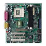
AX59 Pro is a high-performance Pentium®-based system board that utilizes VIA MVP3 AGPset on ATX PCI/ISA platform. This motherboard supports new architectures such as high speed AGP, SDRAM, Ultra DMA/33, Bus master IDE and USB port. It has 512KB or 1MB (optional) pipelined-burst second-level cache onboard and support two single in-line memory module (SIMM) plus three Dual in-line memory module (DIMM) that allows to mix EDO and SDRAM memory and expansion up to a maximum of 1GB.
Not only above features, AX59 Pro implements most advanced technology as following.
Zero Voltage Modem Wake Up In conjunction with ATX soft power On/Off, it is possible to have system totally power off and wakeup to automatically answer a phone call such as answering machine or to send/receive fax. The most important break through is not only external box modem but also internal modem card can be used to support Modem Wake Up. The AX59 Pro and MP56 internal modem card implement special circuit (patent applied) to make sure the modem card work properly without any power.
LAN Wake Up This feature is very similar as Modem Wake Up, but it is through local area network. To use LAN Wake Up function, you must have a network card that supports this feature and also need to install a network management software.
RTC Wake Up Timer The Wake Up Timer is more like an alarm, which wakes up and power on your system at a pre-defined time for specific application. It can be set to wake up everyday or on specific date within a month. The date/time accurate is second.
High Efficient Synchronous Switching Regulator Most of the current switching designs are Asynchronous mode, which from the technical point of view, still consumes very high power as well as heat. AX59 Pro implements high efficient synchronous switching design that the temperature of MOS FET is far less than Schottky diode of Asynchronous design.
CPU Thermal Protection AX59 Pro has a special thermal detection circuit to have warning through application software when the temperature is higher than a predefined value.
CPU core current protection AX59 Pro implements CPU core voltage 15A over-current protection to prevent any accident short circuit and prevent system damage.
CPU and Housing Fan Monitoring AX59 Pro has one more "fan monitoring" function to prevent system overheat. There are two fan connectors, one is for CPU and the other can be a extra housing fan. The system will report and alarm fan malfunction though utility software such as Hardware Monitor utility (named AOhw100, where 100 means version number).
System Voltage Monitoring Further more, AX59 Pro implements a voltage monitoring system. As you turn on your system, this smart design will continue to monitor your system working voltage. If any of the system voltage is over the component's standard. There will be alarm though software such as Hardware Monitor utility for a warning to user.
Full-range CPU core voltage This motherboard supports the CPU core voltage from 1.3V to 3.5V, that can be applied to various CPU type in future.
Resetable Fuse AX59 Pro implements resetable fuses to prevent any accidental short circuit caused by keyboard or USB devices hot plug.
FCC DoC certificate AX59 Pro has passed FCC DoC test. The radiation is very low, you can use any kind of housing.
Powerful utility software supported AOpen Bonus Pack companion CDROM contains many useful utilities, such as Norton Anti-virus, AOchip, Hardware Monitor utility, and BIOS flash utility.
1.1 Specifications
| Form Factor | ATX |
| Board Size | 305 mm x 202 mm |
| CPU | Intel Pentium Processor P54C, PP/MT (P55C), AMD K5/K6/K6-2, Cyrix 6x86/M2 and IDT WinChip C6 family. |
| System Memory | 72-pin SIMM x2, and SDRAM 168-pin x3, maximum 1GB. |
| Second-level Cache | 512KB or 1MB (optional) pipeline-burst cache onboard |
| Chipset | VIA MVP3 AGPset |
| Expansion Slots | ISA x2, PCI x4 and AGP x1 |
| Serial Port | Two serial ports UART 16C550 compatible, and the 3rd UART for IR function. |
| Parallel Port | One parallel port supports standard parallel port (SPP), enhanced parallel port (EPP) or extended capabilities port (ECP). |
| Floppy Interface | Floppy interface supports 3.5 inches drives with 720KB, 1.44MB or 2.88MB format or 5.25 inches drives with 360KB, 1.2MB format. |
| IDE Interface | Dual-channel IDE interface support maximum 4 IDE hard disks or CDROM, mode 4, bus master hard disk drives and Ultra DMA/33 mode hard drives are also supported. |
| USB Interface | Two USB ports supported by USB bracket, the BIOS also supports USB driver to simulate legacy keyboard. |
| PS/2 Mouse | Mini-Din PS/2 mouse connector onboard. |
| Keyboard | Mini-Din PS/2 keyboard connector onboard. |
| RTC and Battery | RTC build in MVP3 chipset, Lithium (CR-2032) battery. |
| BIOS | AWARD Plug-and-Play, 2M bit Flash ROM BIOS. |
| Zero Voltage Modem Wake Up | Special circuit (patent applied) to support modem wake up by external box modem or internal AOpen F56/MP56 modem card. |
| LAN Wake Up | By using a network card that supports this feature and a network management software, you can wake up a system through a local area network. |
| RTC Wake Up Timer | Program the date/time to wake up your system. |
| Synchronous Switching Regulator | High efficient synchronous switching regulator for future CPU. |
| Over-current Protection | CPU core voltage 15A over-current protection to prevent any accident short circuit. |
| CPU Thermal Protection | Warning when CPU temperature is higher than a predefined value. |
| Fan Monitoring | Three fan connectors, warning when CPU or housing fan is malfunction. |
| System Voltage Monitoring | Warning when system voltage (5V,12V,3.3V,2.8V) are abnormal. |
1.2 Overclocking
As a leading manufacturer in motherboard industry, AOpen always listens to what customers want and develop products to fit different user's requirements. Reliability, compatibility, leading technology and friendly features are our basic goals when designing motherboards. Other than above mentioned design criteria, there are power users who are always seeking to push the limitation of the system performance by overclocking which we call them "Overclocker".
This section is dedicated to Overclockers.
This high performance AX59 Pro motherboard is designed for maximum 100MHz CPU bus clock. But it comes with clock generator of 112MHz and 124MHz when we design it to accommodate future CPU bus clock. Our lab test results shown that 112MHz is achievable when proper setting and quality components were presented, we feel quite comfortable overclocking to 112MHz. Not only that, AX59 Pro has 32 Vcore (CPU core voltage) settings and up to 5.5x CPU ratio, that supports almost all of Socket 7 CPUs in the future and provides flexibility for overclockers. As for 124MHz, we do not recommend at this time. For your reference, the following configurations are what we feel comfortable at 112 MHz bus clock. But not guaranty.

Warning: The design of this product follows CPU and chipset vendor's design guideline. Any attempts to push beyond product specification are not recommended and you are taking your own risk to damage your system or important data. Before doing overclocking, you must make sure your components are able to tolerate such abnormal setting, especially CPU, DRAMs, hard disks, and AGP VGA cards.
Warning: Note that overclocking may also cause thermal problem. Please make sure that the cooling fan and the heatsink were adequate to dissipate excessive heat that's generated by overclocking the CPU.
VGA and HDD are key components for overclocking, for your reference, the following list are what have been successful overclocked in our lab. Please note that AOpen can not guaranty they can be successful overclocked again.
VGA Card
| VGA model/ Vendor | Chipset model | Driver |
| Asus | S3 –Virge/dx(86c375) | Asus |
| VENUS T-775 | S3 Trio 64V2(86C775) | Venus |
| VENUS 67TV | Trident 9685 | Venus |
| GALAXIE | Trident 9685 (PS-68) | Venus |
| ATI | MACH 64 210888GX00 | Win95 default |
| MATROX | MY220P/4+ | MGA |
| MATROX | MGA-MIL/4+ | MGA |
| MATROX | MIL2P/4+ | MGA |
Hard Disk:
| Vender | Model | Size |
| Maxtor | 90680D4 | 6.8G |
| Maxtor | 90845D5 | 8.4G |
| Maxtor | 72004AP | 2.0G |
| Maxtor | 82560A4 | 2.5G |
| Seagate | ST36530A | 6.5G |
| Seagate | ST31277A | 1.2G |
| Quantum | FireballST4320AT | 4.3G |
| Quantum | T-Rex Bigfoot TX6.0AT | 6.0G |
| Quantum | T-Rex Bigfoot TX8.0AT | 8.0G |
| Quantum | T-Rex Bigfoot TX12.0AT | 12.0G |
| IBM | DHEA-34330 | 4.3G |
| IBM | DTTA-351010 | 10.1G |
| IBM | DTTA-350840 | 8.4G |
| IBM | DTTA-350640 | 6.4G |
| IBM | DAQA-32160 | 2.1G |
AX59 Pro Overclocking Settings
The following table lists the overlapping settings in AOpen's lab for your reference.
| CPU | Intel MMX-233MHz |
| DRAM | SEC KOREA 801 KM48S2020CT-GH 32MB |
| HDD | IBM DHEA-34330 |
| VGA | ATI 3D RAGE PRO AGP 2X |
| OS | Windows 95 OSR2 |
| BIOS | R2.00d Load BIOS Setup Default for 112MHz * 2.5 = 280MHz (O.K.) 112MHz * 2 = 224MHz (O.K.) Load BIOS Turbo Default for 100MHz * 2.5 = 250MHz (O.K.) |
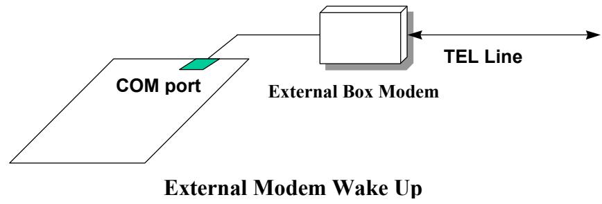
1.3 Zero Voltage Modem Wake Up
The Modem Wake Up discussed here is to wakeup from true power off (identified by fan of power supply is off), This motherboard still supports traditional green PC suspend mode but it is not discussed here.
With the help ATX soft power On/Off, it is possible to have system totally power off (The traditional suspend mode of power management function does not really turn off the system power supply), and wakeup to automatically answer a phone call such as answering machine or to send/receive fax. You may identify the true power off by checking fan of your power supply. Both external box modem and internal modem card can be used to support Modem Wake Up, but if you use external modem, you have to keep the box modem always power-on. AOpen AX59 Pro and internal modem card implement special circuit (patent applied) and make sure the modem card works properly without any power. We recommend you choose AOpen modem card (MP56) for Modem Wake Up applications.

Internal Modem Card Wake Up (such as MP56)
For Internal Modem Card (AOpen MP56):
- Go into BIOS setup, Power Management Modem Wake Up, select Enable.
- Setup your application, put into Windows 95.
- Turn system power off by soft power switch.
- Connect 4-pin Modem Ring-On cable from MP56 RING connector to AX59 Pro connector WKUP.
- Connect telephone line to MP56. You are now ready to use Modem Ring-On.
For External Box Modem:
- Go into BIOS setup, Power Management Modem Wake Up, select Enable.
- Setup your application, put into Windows 95 Start Up.
- Turn system power off by soft power switch.
- Connect RS232 cable of external box Modem to COM1 or COM2.
- Connect telephone line to external box Modem. Turn on Modem power (you must keep Modem power always on). You are now ready to use Modem Ring

Tip: External modem wake up signal is detected through COM1 or COM2. Internal modem card wake up signal is detected through cable from connector RING (on modem card) to WKUP (on mainboard).

Note: If you use external modem, the power of external modem must be kept on to receive signal from telephone line. Internal modem card has no such limitation.
1.4 System Voltage Monitoring
This motherboard implements a voltage monitoring system. As you turn on your system, this smart design will continue to monitor your system working voltage. If any of the system voltage is over the component's standard. There will be alarm through application software such as Hardware Monitor utility for a warning to user. System voltage monitoring function monitors CPU core voltage. It is automatically implemented by BIOS and Hardware Monitor utility (the file name is like aohw100.exe, where 100 means the version number, no hardware installation is needed.
1.5 Fan Monitoring
There are three fan connectors, two is for CPU, the other can be a housing fan. The fan monitoring function is implemented by connecting fan to 3-pin fan connector CPUFAN2 and installing Hardware Monitor utility.

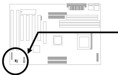
Note: You need 3-pin fan that supports SENSE signal for fan monitoring function to work properly.
1.6 CPU Thermal Protection
This motherboard implements special thermal protection circuit below the CPU. When temperature is higher than a predefined value, the CPU speed will automatically slow down and there will be warning from BIOS and also Hardware Monitoring Utility software.
CPU Thermal Protection is automatically implemented by BIOS and utility software, no hardware installation is needed.
Chapter 2
Hardware Installation
This chapter gives you a step-by-step procedure on how to install your system. Follow each section accordingly.

Caution: Electrostatic discharge (ESD) can damage your processor, disk drives, expansion boards, and other components. Always observe the following precautions before you install a system component.
- Do not remove a component from its protective packaging until you are ready to install it.
- Wear a wrist ground strap and attach it to a metal part of the system unit before handling a component. If a wrist strap is not available, maintain contact with the system unit throughout any procedure requiring ESD protection.
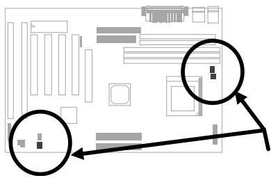
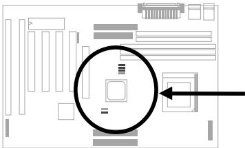
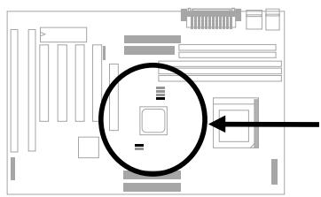
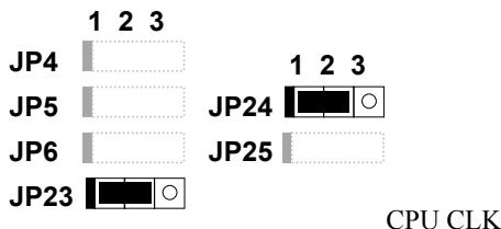
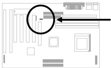
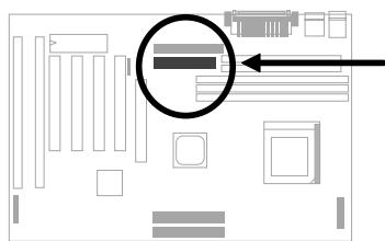
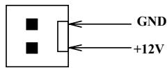
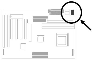
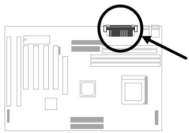
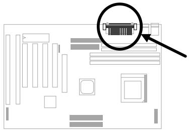
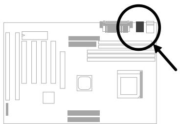
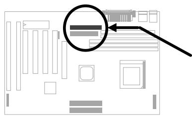
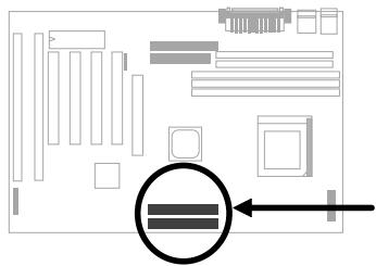
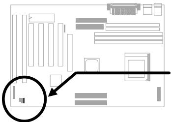
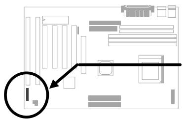
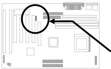
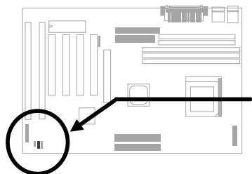
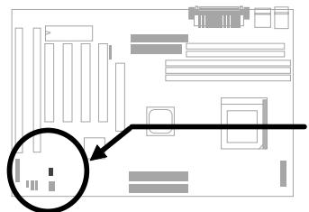
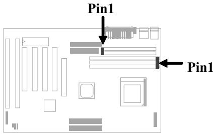
2.1 Jumper and Connector Locations
The following figure shows the locations of the jumpers and connectors on the system board :
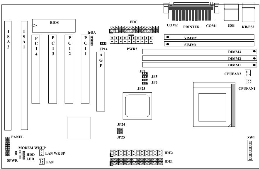
Jumpers:
SW1: DIP Switch for CPU voltage and clock ratio
JP4,JP5,JP6, CPU external (bus) clock
JP25:
JP23,JP24 DRAM Clock
JP14: Clear CMOS
Connectors:
PS2: PS/2 mouse connector
KB: PS/2 keyboard connector
PWR2: ATX power connector
USB: USB connector
FDC: Floppy drive connector
IDE1: IDE1 primary channel
IDE2: IDE2 secondary channel
CPUFAN1: CPU Fan connector
CPUFAN2: CPU Fan connector
FAN: Fan Connector
IrDA: IrDA (Infrared) connector
HDD LED: HDD LED connector
PANEL: Front panel (Multifunction) connector
SPWR: ATX Soft-Power Switch Connector
MODEM-WKUP: MODEM Wake Up Connector
LAN-WKUP: LAN Wake Up Connector
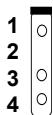
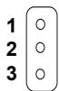
2.2 Jumpers
J jumpers are made by pin headers and plastic connecting caps for the purpose of customizing your hardware. Doing so requires basic knowledge of computer hardware, be sure you understand the meaning of the jumpers before you change any setting. The onboard jumpers are normally set to their default with optimized settings.
On the mainboard, normally there is a bold line marked beside pin 1 of the jumper, sometimes, there are numbers also. If we connect (short) plastic cap to pin 1 and 2, we will say set it at 1-2, and when we say jumper is open, that means no plastic cap connected to jumper pins.

Open

Short

Jumper set at 1-2

Jumper set at 2-3
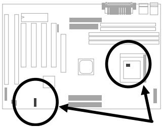
For your convenience to install a CPU, this motherboard also use a DIP switch to set CPU voltage and frequency ratio. The following figure simply shows you how to set this DIP switch, please see also to next sections for more details.
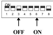
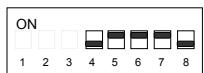
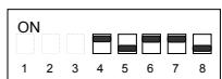
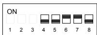
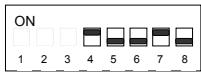
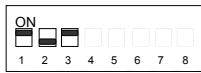
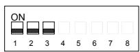
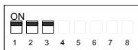
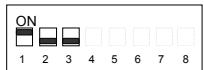
2.2.1 Setting the CPU Voltage
SW1 is used to select CPU core voltage (Vcore) and ratio, there are totally eight switches on the DIP. After installing CPU, set the switch 4-8 to specify a proper Vcore.
3.52V
6x86 or K5
3.45V
P54C
3.3V
IDTC6
3.2V
K6-233
2.9V
K6-166/200 or M2
2.8V
P55C (MMX)
2.4V
K6-2 400/450 and K6-III
2.2V
K6-266/300 and K6-2
Following table lists possible settings of current CPU available on the market. Note that the correct setting may vary because of new CPU product, refer to your CPU specification for more details.
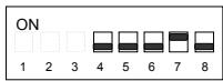
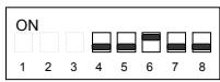
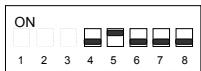
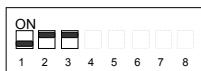
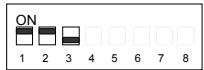
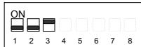
| CPU | Type | Vcore | S4 | S5 | S6 | S7 | S8 |
| INTEL P54C | Single Voltage | 3.45V | OFF | ON | ON | ON | OFF |
| INTEL P55C | Dual Voltage | 2.8V | OFF | OFF | OFF | ON | OFF |
| AMD K5 | Single Voltage | 3.52V | ON | ON | ON | ON | OFF |
| AMD K6-166/200 | Dual Voltage | 2.9V | ON | OFF | OFF | ON | OFF |
| AMD K6-233 | Dual Voltage | 3.2V | OFF | OFF | ON | ON | OFF |
| AMD K6-266/300 | Dual Voltage | 2.2V | OFF | ON | OFF | OFF | OFF |
| AMD K6-2 | Dual Voltage | 2.2V | OFF | ON | OFF | OFF | OFF |
| AMD K6-2 400/450 | Dual Voltage | 2.4V | OFF | OFF | ON | OFF | OFF |
| AMD K6-III | Dual Voltage | 2.4V | OFF | OFF | ON | OFF | OFF |
| Cyrix 6x86 | Single Voltage | 3.52V | ON | ON | ON | ON | OFF |
| Cyrix 6x86L | Dual Voltage | 2.8V | OFF | OFF | OFF | ON | OFF |
| Cyrix M2 | Dual Voltage | 2.9V | ON | OFF | OFF | ON | OFF |
| IDT C6 | Single Voltage | 3.52V | ON | ON | ON | ON | OFF |
| 3.3V | ON | OFF | ON | ON | OFF |

Warning: This high performance AX59 Pro motherboard that AOpen presented to you has a capability to overclock to 112MHz external clock while still conforming the design guide from VIA. This overclock scheme is accomplished by AOpen's technical expertise as well as manufacturing capabilities. However, please understand that some of the add-on cards might not work with this board properly when overclock scheme is engaged. Please use designated speed when you encountered such a problem

Warning: Note that overclocking may cause thermal problem. Please make sure that the cooling fan and the heatsink were adequate to dissipate excessive heat that's generated by overclocking the CPU.
Tip: Normally, for single voltage CPU, Vcpuio (CPU I/O Voltage) is equal to Vcore, but for CPU that needs dual voltage such as PP/MT (P55C) or Cyrix 6x86L, Vcpuio is different from Vcore and must be set to Vio (PBSRAM and Chipset Voltage). The single or dual voltage CPU is automatically detected by hardware circuit.
Tip: For supporting more different CPUs in future, this motherboard uses five switches to specify Vcore. There are 32 settings totally, and the range is from 1.3V to 3.5V.
This motherboard supports the CPU core voltage from 1.3V to 3.5V, that can be applied to the various CPU type in future. For your reference, all settings are listed in the following table.
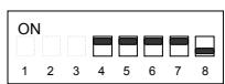
2.2.2 Selecting the CPU Frequency
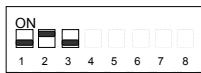
| S1 | S2 | S3 | CPU Frequency Ratio |
| OFF | OFF | OFF | 1.5x (3.5x) |
| ON | OFF | OFF | 2x |
| ON | ON | OFF | 2.5x (1.75x) |
| OFF | ON | OFF | 3x |
| ON | OFF | ON | 4x |
| ON | ON | ON | 4.5x |
| OFF | ON | ON | 5x |
| OFF | OFF | ON | 5.5x |
Intel Pentium, Cyrix 6x86 and AMD K5/K6 CPU are designed to have different Internal (Core) and External (Bus) frequency. The ratio of Core/Bus frequency is selected by the switch 1-3 of SW1.

Note: Intel PP/MT MMX 233MHz is using 1.5x jumper setting for 3.5x frequency ratio, and AMD PR166 is using 2.5x setting for 1.75x frequency ratio.
Core frequency = Ratio * External bus clock

3x
4x
1.5x (3.5x)
4.5x
2x
5x
2.5x (1.75x)
5.5x
JP4, JP5, JP6 and J25 are the selections of CPU external clock (bus clock), AGP Clock and PCI Clock.
75MHz
83MHz
66MHz
68MHz

95MHz
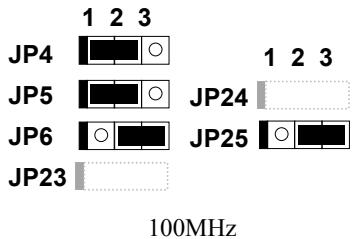
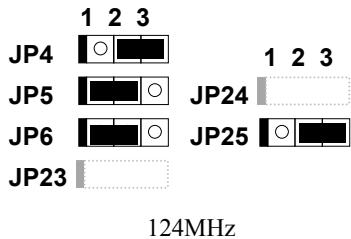
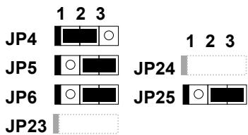
112MHz

Warning: VIA MVP3 chipset supports maximum 100MHz external CPU bus clock, the 112MHz settings are for internal test only, set to 112 or 124 MHz exceeds the specification of MVP3 chipset, which may cause serious system damage.
Warning: While 100/112/124 MHz is selected, we strongly recommend you to choose PC100 SDRAM for system stability.

Caution: The following table are possible settings of current CPU available on the market. The correct setting may vary because of new CPU product, refer to your CPU specification for more details.
| INTEL Pentium | CPU Core Frequency | Ratio | External Bus Clock | S1 | S2 | S3 | JP4,JP5,JP6,JP25 |
| P54C 100 | 100MHz = | 1.5x | 66MHz | OFF | OFF | OFF | 1-2 & 1-2 & 1-2 & 1-2 |
| P54C 133 | 133MHz = | 2x | 66MHz | ON | OFF | OFF | 1-2 & 1-2 & 1-2 & 1-2 |
| P54C 166 | 166MHz = | 2.5x | 66MHz | ON | ON | OFF | 1-2 & 1-2 & 1-2 & 1-2 |
| P54C 200 | 200MHz = | 3x | 66MHz | OFF | ON | OFF | 1-2 & 1-2 & 1-2 & 1-2 |
| INTEL Pentium MMX | CPU Core Frequency | Ratio | External Bus Clock | S1 | S2 | S3 | JP4,JP5,JP6,JP25 |
| PP/MT 166 | 166MHz = | 2.5x | 66MHz | ON | ON | OFF | 1-2 & 1-2 & 1-2 & 1-2 |
| PP/MT 200 | 200MHz = | 3x | 66MHz | OFF | ON | OFF | 1-2 & 1-2 & 1-2 & 1-2 |
| PP/MT 233 | 233MHz = | 3.5x | 66MHz | OFF | OFF | OFF | 1-2 & 1-2 & 1-2 & 1-2 |
| Cyrix 6x86 & 6x86L | CPU Core Frequency | Ratio | External Bus Clock | S1 | S2 | S3 | JP4,JP5,JP6,JP25 |
| P166+ | 133MHz = | 2x | 66MHz | ON | OFF | OFF | 1-2 & 1-2 & 1-2 & 1-2 |
| P200+ | 150MHz = | 2x | 75MHz | ON | OFF | OFF | 1-2 & 2-3 & 1-2 & 1-2 |
| Cyrix M2 | CPU Core Frequency | Ratio | External Bus Clock | S1 | S2 | S3 | JP4,JP5,JP6,JP25 |
| MX-PR200 | 166MHz = 150MHz= | 2.5x | 66MHz | ON | ON | OFF | 1-2 & 1-2 & 1-2 & 1-2 |
| 2x | 75MHz | ON | OFF | OFF | 1-2 & 2-3 & 1-2 & 1-2 | ||
| MX-PR233 | 200MHz = 166MHz= | 3x | 66MHz | OFF | ON | OFF | 1-2 & 1-2 & 1-2 & 1-2 |
| 2x | 83.3MHz | ON | OFF | OFF | 2-3 & 2-3 & 1-2 & 2-3 | ||
| MX-PR266 | 233MHz = | 3.5x | 66MHz | OFF | OFF | OFF | 1-2 & 1-2 & 1-2 & 1-2 |
| MX-PR300 | 225MHz= 233MHz= | 3x | 75MHz | OFF | ON | OFF | 1-2 & 2-3 & 1-2 & 1-2 |
| 3.5x | 66MHz | OFF | OFF | OFF | 1-2 & 1-2 & 1-2 & 1-2 |
| IDT C6 | CPU Core Frequency | Ratio | External Bus Clock | S1 | S2 | S3 | JP4,JP5,JP6,JP25 |
| C6-150 | 150MHz = | 2x | 75MHz | ON | OFF | OFF | 1-2 & 2-3 & 1-2 & 1-2 |
| C6-200 | 200MHz = | 3x | 66MHz | OFF | ON | OFF | 1-2 & 1-2 & 1-2 & 1-2 |
| AMD K5 | CPU Core Frequency | Ratio | External Bus Clock | S1 | S2 | S3 | JP4,JP5,JP6,JP25 |
| PR100 | 100MHz = | 1.5x | 66MHz | OFF | OFF | OFF | 1-2 & 1-2 & 1-2 & 1-2 |
| PR133 | 100MHz = | 1.5x | 66MHz | OFF | OFF | OFF | 1-2 & 1-2 & 1-2 & 1-2 |
| PR166 | 116MHz = | 1.75x | 66MHz | ON | ON | OFF | 1-2 & 1-2 & 1-2 & 1-2 |
| AMD K6 | CPU Core Frequency | Ratio | External Bus Clock | S1 | S2 | S3 | JP4, JP5, JP6, JP25 |
| K6-166 | 166MHz = | 2.5x | 66MHz | ON | ON | OFF | 1-2 & 1-2 & 1-2 & 1-2 |
| K6-200 | 200MHz = | 3x | 66MHz | OFF | ON | OFF | 1-2 & 1-2 & 1-2 & 1-2 |
| K6-233 | 233MHz = | 3.5x | 66MHz | OFF | OFF | OFF | 1-2 & 1-2 & 1-2 & 1-2 |
| K6-266 | 266MHz= | 4x | 66MHz | ON | OFF | ON | 1-2 & 1-2 & 1-2 & 1-2 |
| K6-300 | 300MHz= | 4.5x | 66MHz | ON | ON | ON | 1-2 & 1-2 & 1-2 & 1-2 |
| K6-2 333 | 333MHz | 3.5x | 95MHz | OFF | OFF | OFF | 2-3 & 1-2 & 2-3 & 2-3 |
| K6-2 350 | 350MHz | 3.5x | 100MHz | OFF | OFF | OFF | 1-2 & 1-2 & 2-3 & 2-3 |
| K6-2 366 | 366MHz | 5.5x | 66MHz | OFF | OFF | ON | 1-2 & 1-2 & 1-2 & 1-2 |
| K6-2 380 | 380MHz | 4x | 95MHz | ON | OFF | ON | 2-3 & 1-2 & 2-3 & 2-3 |
| K6-2 400 | 400MHz | 4x | 100MHz | ON | OFF | ON | 1-2 & 1-2 & 2-3 & 2-3 |
| K6-2 450 | 450MHz | 4.5x | 100MHz | ON | ON | ON | 1-2 & 1-2 & 2-3 & 2-3 |
| K6-III 400 | 400MHz | 4x | 100MHz | ON | OFF | ON | 1-2 & 1-2 & 2-3 & 2-3 |
| K6-III 450 | 450MHz | 4.5 | 100MHz | ON | ON | ON | 1-2 & 1-2 & 2-3 & 2-3 |

Note: Cyrix 6x86, 6x86MX (M2) and AMD K5 CPU use P-rating for the reference of CPU benchmark compared with INTEL P54C, their internal core frequency is not exactly equal to P-rating marked on the CPU. For example, Cyrix P166+ is 133MHz but performance is almost equal to P54C 166MHz and AMD PR133 is 100MHz but performance is almost equal to INTEL P54C 133MHz.
2.2.3 DRAM Clock
| JP23 | JP24 | DRAM CLK |
| 1-2 | 1-2 | CPU CLK |
| 2-3 | 2-3 | AGP CLK |
JP23, JP24 are used to decide if DRAM clock is synchronous with CPU or AGP clock.
123
JP4

123
JP5

JP24

JP6

JP25

JP23

AGP CLK
2.2.4 Clearing the CMOS
JP14 Clear CMOS
1-2 Normal operation (default)
2-3 Clear CMOS
You need to clear the CMOS if you forget your system password. To clear the CMOS, follow the procedures listed below:

JP14
Normal Operation (default)

JP14
Clear CMOS
The procedure to clear CMOS:
- Turn off the system and unplug the AC power.
- Remove ATX power cable from connector PWR2.
- Locate JP14 and short pins 2-3 for a few seconds.
- Return JP14 to its normal setting by shorting pins 1-2.
- Connect ATX power cable back to connector PWR2.
- Turn on the system power.
- Press DEL during bootup to enter the BIOS Setup Utility and specify a new password, if needed.
2.3 Connectors
2.3.1 Power Cable
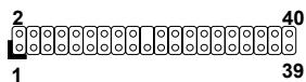
The ATX power supply uses 20-pin connector shown below. Make sure you plug in the right direction.

Caution: Make sure that the power supply is off before connecting or disconnecting the power cable.
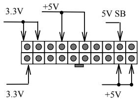
PWR2
2.3.2 ATX Soft-Power Switch Connector
The ATX soft-power switch connector is a 2-pin header on the system board. Locate the power switch cable from your ATX housing. It is 2-pin female connector from the housing front panel. Plug this connector to the soft-power switch connector marked SPWR.

1 2
SPWR
2.3.3 Fan
Plug in the fan cable to the fan connectors onboard. The fan connectors are marked CPUFAN1, CPUFAN2 and FAN on the system board. You can plug the CPU fan cable to both the 2-pin fan connector CPUFAN1 and the 3-pin fan connector CPUFAN2. FAN can be reserved for the housing fan. Note that only CPUFAN2 and FAN support the fan monitoring function, because 3-pin fan has an extra pin called SENSE, which periotically sends fan signal out.

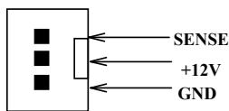
CPUFAN2 & FAN
CPUFAN1
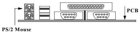
2.3.4 PS/2 Mouse
The onboard PS/2 mouse connector is a 6-pin Mini-Din connector marked PS2. MS. The view angle of drawing shown here is from back panel of the housing.
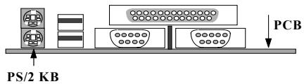
2.3.5 Keyboard
The onboard PS/2 keyboard connector is a 6-pin Mini-Din connector marked KB. The view angle of drawing shown here is from back panel of the housing.
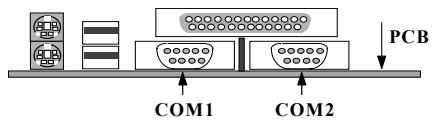
2.3.6 Serial Devices (COM1/COM2)
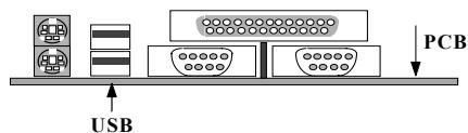
The onboard serial connectors are 9-pin D-type connector on the back panel of mainboard. The serial port 1 connector is marked as COM1 and the serial port 2 connector is marked as COM2.
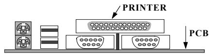
2.3.7 Printer
The onboard printer connector is a 25-pin D-type connector marked PRINTER. The view angle of drawing shown here is from back panel of the housing.
2.3.8 USB Device
You can attach USB devices to the USB connector. The motherboard contains two USB connectors, which are marked as USB.
2.3.9 Floppy Drive
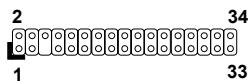
Connect the 34-pin floppy drive cable to the floppy drive connector marked as FDC on the system board.
FDC
2.3.10 IDE Hard Disk and CD ROM
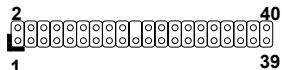
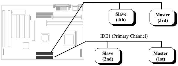
This motherboard supports two 40-pin IDE connectors marked as IDE1 and IDE2. IDE1 is also known as primary channel and IDE2 as secondary channel, each channel supports two IDE devices that makes total of four devices.
In order to work together, the two devices on each channel must be set differently to master and slave mode, either one can be hard disk or CDROM. The setting as master or slave mode depends on the jumper on your IDE device, please refer to your hard disk and CDROM manual accordingly.
Connect your first IDE hard disk to master mode of the primary channel. If you have second IDE device to install in your system, connect it as slave mode on the same channel, and the third and fourth device can be connected on secondary channel as master and slave mode respectively.
IDE2
IDE1

Caution: The specification of IDE cable is maximum 46cm (18 inches), make sure your cable does not excess this length.
Caution: For better signal quality, it is recommended to set far end side device to master mode and follow the suggested sequence to install your new device. Please refer to following figure.
IDE2 (Secondary Channel)
2.3.11 Hard Disk LED
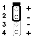
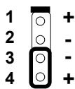
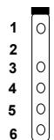
The HDD LED connector is marked as HDD LED on the board. This connector is designed for different type of housing, actually only two pins are necessary for the LED. If your housing has four pin connector, simply plug it in. If you have only two pin connector, please connect to pin 1-2 or pin 3-4 according to the polarity.
Pin Description
1 HDDLED
2 GND
3 GND
4 HDDLED

HDD LED
4-pin connector
HDD LED
2-pin connector at pin 1-2
HDD LED
2-pin connector at pin 3-4
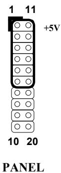
2.3.12 Panel Connector
The Panel (multifunction) connector is a 20-pin connector marked as PANEL on the board. Attach the power LED, keylock, speaker, and reset switch to the corresponding pins as shown in the figure.
Some housings have a five-pin connector for the keylock and power LED Since power LED and keylock are aligned together, you can still use this kind of connector.
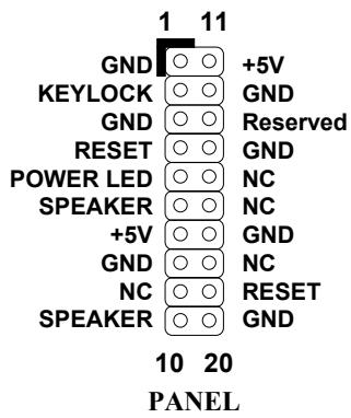
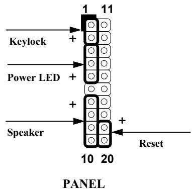
Other housings may have a 12-pin connector. If your housing has this type of connector, connect it to PANEL as shown in the figure. Make sure that the red wire of the connector is connected to +5V .
2.3.13 IrDA Connector
The IrDA connector can be configured to support wireless infrared module, with this module and application software such as Laplink or Win95 Direct Cable Connection, user can transfer files to or from laptops, notebooks, PDA and printers. This connector supports HPSIR (115.2Kbps, 2 meters), ASK-IR (56Kbps) and Fast IR (4Mbps, 2 meters).
Install infrared module onto IrDA connector and enable infrared function from BIOS setup, make sure to have correct orientation when you plug onto IrDA connector.
| Pin | Description |
| 1 | +5V |
| 2 | NC |
| 3 | IRRX |
| 4 | GND |
| 5 | IRTX |
| 6 | NC |
IrDA
2.3.14 Wake-up Connector
This mainboard implements special circuit to support Modem Ring-On, both Internal Modem Card (AOpen MP56) and external box Modem are supported. Since Internal Modem card consumes no power when system power is off, it is recommended to use Internal Modem. To use AOpen MP56, connect 4-pin cable from RING connector of MP56 to WKUP connector on the mainboard.
| Pin | Description |
| 1 | +5V SB |
| 2 | NC |
| 3 | RING |
| 4 | GND |

Tip: Not only for Modem Ring-On, there are many other possible applications. For example, IR wakeup or voice wakeup.
Modem-WKUP
2.3.15 LAN Wake-up Connector
This mainboard implements a LAN-WKUP connector. To use LAN Wake-up function, you need a network card that supports this feature. In addition, you also need to install a network management software, such as ADM.
| Pin | Description |
| 1 | +5V SB |
| 2 | GND |
| 3 | LID |
LAN-WKUP
2.4 Configuring the System Memory
This motherboard has two 72 pin SIMM sockets (Single-in-line Memory Module) and three 168 pin DIMM socket (Dual-in-line Memory Module) that allow you to install system memory maximum 1GB.
The SIMM supported by this mainboard can be identified by 4 kinds of factors:
I. Size: single side, 1Mx32 (4MB), 4Mx32 (16MB), 16Mx32 (64MB), and double side, 1Mx32x2 (8MB), 4Mx32x2 (32MB), 16Mx32x2 (128MB).
II. Speed: 60ns or 70ns access time
III. Type: FPM (Fast page mode) or EDO (Extended data output)
IV. Parity: without parity (32 bit wide) or with parity (36 bit wide).
DIMM modules can be identified by following factors:
I. Size: single side, 1Mx64 (8MB), 2Mx64 (16MB), 4Mx64 (32MB), 8Mx64 (64MB), 16Mx64 (128MB), and double side, 1Mx64x2 (16MB), 2Mx64x2 (32MB), 4Mx64x2 (64MB), 8Mx64x2 (128MB).

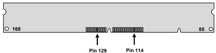
Tip: Here is a trick to check if your DIMM is single-side or double-side -- if there are traces connected to golden finger pin 114 and pin 129 of the DIMM, the DIMM is probably double-side; otherwise, it is single-side. Following figure is for your reference.
II. Speed: normally marked as -12, which means the clock cycle time is 12ns and maximum clock of this SDRAM is 83MHz. Sometimes you can also find the SDRAM marked as -67, which means maximum clock is 67mhz.

Caution: Some SDRAMs marked as -10 may work fine with 100 MHz CPU clock, but not all this kind of modules can work properly under 100MHz external clock. We suggest you choose and install SDRAMs that match PC 100 specification if 100MHz or above CPU clock is selected.
III. Buffered and non-buffered: This motherboard supports non-buffered DIMMs. You can identify non-buffered DIMMs and buffered DIMMs according to the position of the notch, following figure is for your reference:
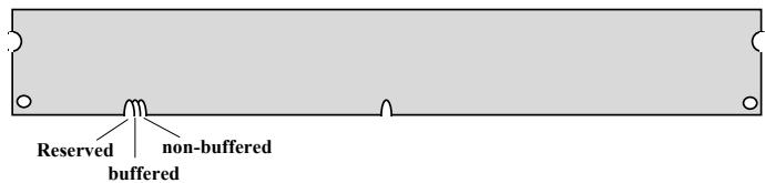
Because the positions are different, only non-buffered DIMMs can be inserted into the DIMM sockets on this motherboard. Although most of DIMMs on current market are non-buffered, we still recommend you to ask your dealer for the correct type.
IV. 2-clock and 4-clock signals: Although both of 2-clock and 4-clock signals are supported by this motherboard, we strongly recommend you to choose 4-clock SDRAM in consideration of reliability.

Tip: To identify 2-clock and 4-clock SDRAM, you may check if there are traces connected to golden finger pin 79 and pin 163 of the SDRAM. If there are traces, the SDRAM is probably 4-clock; Otherwise, it is 2-clock.
V. Parity: This motherboard supports standard 64 bit wide (without parity) SDRAM.
There is no jumper setting required for the memory size or type. It is automatically detected by the system BIOS.
Total Memory Size = Size of SIMM1 + Size of SIMM2 + Size of DIMM1 + Size of DIMM2 + Size of DIMM3

Caution: Note that DIMM3 shares a bank with SIMM1 and SIMM2, so you couldn't use a doulbe side DIMM if SIMMs were installed.
Caution: There are some old DIMMs made by EDO or FPM memory chip, they can only accept 5V power and probably cannot fit into the DIMM socket, make sure you have 3.3V true SDRAM DIMM before your insert it.
There is an important parameter affects SDRAM performance, CAS Latency Time. It is similar as CAS Access Time of EDO DRAM and is calculated as number of clock state. If your SDRAM has unstable problem, go into BIOS "Chipset Features Setup", change CAS Latency Time to 3 clocks.
The driving capability of new generation chipset is limited because the lack of memory buffer (to improve performance). This makes DRAM chip count an important factor to be taking into consideration when you install DIMM. Unfortunately, there is no way that BIOS can identify the correct chip count, you need to calculate the chip count by yourself. The simple rule is: By visual inspection, use only DIMM which is less than 16 chips.

Warning: Although this motherboard supports x4 SDRAM chip. Due to loading issue, it is not recommended to use this kind of SDRAM.

Tip: The DIMM chip count can be calculated by following example:
- For 32 bit non-parity SIMM using 1M by 4 bit DRAM chip, 32/4 = 8 chips.
- For 36 bit parity SIMM using 1M by 4 bit DRAM chip, 36/4=9 chips.
- For 36 bit parity SIMM using 1M by 4 bit and 1M by 1 bit DRAM, the chip count will be 8 data chips(8=32/4) plus 4 parity chips(4=4/1), total is 12 chips.
- For 64 bit DIMM using 1M by 16 bit SDRAM, the chip count is 64 / 16 = 4 chips.
Following table list the recommended DRAM combinations of SIMM and DIMM:
| SIMM Data chip | SIMM Parity chip | Bit size per side | Single/ Double side | Chip count | SIMM size | Recommended |
| 1M by 4 | None | 1Mx32 | x1 | 8 | 4MB | Yes |
| 1M by 4 | None | 1Mx32 | x2 | 16 | 8MB | Yes |
| 1M by 4 | 1M by 1 | 1Mx36 | x1 | 12 | 4MB | Yes |
| 1M by 4 | 1M by 4 | 1Mx36 | x1 | 9 | 4MB | Yes |
| 1M by 4 | 1M by 4 | 1Mx36 | x2 | 18 | 8MB | Yes |
| 1M by 16 | None | 1Mx32 | x1 | 2 | 4MB | Yes |
| 1M by 16 | None | 1Mx32 | x2 | 4 | 8MB | Yes |
| 1M by 16 | 1M by 4 | 1Mx36 | x1 | 3 | 4MB | Yes |
| 1M by 16 | 1M by 4 | 1Mx36 | x2 | 6 | 8MB | Yes |
| 4M by 4 | None | 4Mx32 | x1 | 8 | 16MB | Yes |
| 4M by 4 | None | 4Mx32 | x2 | 16 | 32MB | Yes |
| 4M by 4 | 4M by 1 | 4Mx36 | x1 | 12 | 16MB | Yes |
| 4M by 4 | 4M by 1 | 4Mx36 | x2 | 24 | 32MB | Yes |
| SIMM Data chip | SIMM Parity chip | Bit size per side | Single/ Double side | Chip count | SIMM size | Recommended |
| 16M by 4 | None | 16Mx32 | x1 | 8 | 64MB | Yes, but not tested. |
| 16M by 4 | None | 16Mx32 | x2 | 16 | 128MB | Yes, but not tested. |
| 16M by 4 | 16M by 4 | 16Mx36 | x1 | 9 | 64MB | Yes, but not tested. |
| 16M by 4 | 16M by 4 | 16Mx36 | x2 | 18 | 128MB | Yes, but not tested. |
| DIMM Data chip | Bit size per side | Single/ Double side | Chip count | DIMM size | Recommended |
| 1M by 16 | 1Mx64 | x1 | 4 | 8MB | Yes |
| 1M by 16 | 1Mx64 | x2 | 8 | 16MB | Yes |
| 2M by 8 | 2Mx64 | x1 | 8 | 16MB | Yes |
| 2M by 8 | 2Mx64 | x2 | 16 | 32MB | Yes |
| DIMM | Bit size | Single/ | Chip | DIMM size | Recommended |
| Data chip | per side | Double side | count | ||
| 2M by 32 | 2Mx64 | x1 | 2 | 16MB | Yes, but not tested. |
| 2M by 32 | 2Mx64 | x2 | 4 | 32MB | Yes, but not tested. |
| 4M by 16 | 4Mx64 | x1 | 4 | 32MB | Yes, but not tested. |
| 4M by 16 | 4Mx64 | x2 | 8 | 64MB | Yes, but not tested. |
| 8M by 8 | 8Mx64 | x1 | 8 | 64MB | Yes, but not tested. |
| 8M by 8 | 8Mx64 | x2 | 16 | 128MB | Yes, but not tested. |

Tip: 8 bit = 1 byte, 32 bit = 4 byte. The SIMM size is represented by number of data byte (whether with or without parity), for example, the size of single side SIMM using 1M by 4 bit chip is 1Mx32 bit, that is, 1M x 4 byte=4MB. For double side SIMM, simply multiply it by 2, that is, 8MB.
Following table are possible DRAM combinations that is NOT recommended:
| SIMM Data chip | SIMM Parity chip | Bit size per side | Single/ Double side | Chip count | SIMM size | Recommended |
| 1M by 1 | None | 1Mx32 | x1 | 32 | 4MB | No |
| 1M by 1 | 1M by 1 | 1Mx36 | x1 | 36 | 4MB | No |
| 1M by 4 | 1M by 1 | 1Mx36 | x2 | 24 | 8MB | No |
| 4M by 1 | None | 4Mx32 | x1 | 32 | 16MB | No |
| 4M by 1 | 4M by 1 | 4Mx36 | x1 | 36 | 16MB | No |
| 16M by 1 | None | 16Mx32 | x1 | 32 | 64MB | No |
| 16M by 1 | 16M by 1 | 16Mx36 | x1 | 36 | 64MB | No |
| DIMM Data chip | Bit size per side | Single/ Double side | Chip count | DIMM size | Recommended |
| 4M by 4 | 4Mx64 | x1 | 16 | 32MB | No |
| 4M by 4 | 4Mx64 | x2 | 32 | 64MB | No |
| 16M by 4 | 16Mx64 | x1 | 16 | 128MB | No |
For getting the best performance and stability under 100MHz or above external clock, we strongly recommend you use PC 100 SDRAM. The PC 100 SDRAM that AOpen had tested are listed below.
| Size | Vendor | Model | Single/Double | Chip Count |
| 16M | Hyundai | HY57V168010CTC-10 | x1 | 8 |
| 32M | NEC | D4516821AG5-A10-7JF | x1 | 16 |
| 32M | SEC | KM48S2020CT-GH | x2 | 18 |
| 32M | Hyundai | HY57V168010CTC-10 | x2 | 16 |
| 32M | Micron | MT48LC2M8A1-08 | x2 | 16 |
| 32M | Fujitsu | 81F16822D-A10-7JF | x2 | 18 |
| 64M | Mitsubishi | M5M4V64S30ATP -10 | x1 | 9 |
| 64M | Fujitsu | 81F64842B-103FN | x1 | 9 |
| 64M | NEC | D4564841G5-A10-9JF | x1 | 9 |
| 64M | SEC | KM48S8030BT-GH | x1 | 9 |
| 64M | Toshiba | TC59S6408FTL-80H | x1 | 9 |
Memory error checking is supported by parity check. To use parity check you need 36 bit SIMM (32 bit data + 4 bit parity), which are automatically detected by BIOS.

Tip: The parity mode uses 1 parity bit for each byte, normally it is even parity mode, that is, each time the memory data is updated, parity bit will be adjusted to have even count "1" for each byte. When next time, if memory is read with odd number of "1", the parity error is occurred and this is called single bit error detection.
2.5 Windows 98 Installation
For installing Windows 98, please make sure you have followed below procedures.
- First, don't install any add-on card except the display card.
- Enable USB Controller in BIOS Setup menu, making BIOS fully capable of controlling IRQ assignment.
- Install Window 98 into your system.
- If you use an AGP card, you still need to Install the VIA AGP Driver.
- Then install drivers that come with your AGP card.
- Install the VIA IRQ routing driver, which will correct the partially wrong IRQ routing table for MVP3 chipset in Windows 98.
- Finally, Install other add-on cards.
In the AOpen Bonus Pack CDROM, you can find above drivers in the path X:\Ax59pro\Driver (Where X: represents your CDROM drive).
Chapter 3
Award BIOS
This chapter tells how to configure the system parameters. You may update your BIOS via AWARD Flash Utility.

Important: Because the BIOS code is the most often changed part of the mainboard design, the BIOS information contained in this chapter (especially the Chipset Setup parameters) may be a little different compared to the actual BIOS that came with your mainboard.
3.1 Entering the Award BIOS Setup Menu
The BIOS setup utility is a segment of codes/routines residing in the BIOS Flash ROM. This routine allows you to configure the system parameters and save the configuration into the 128 byte CMOS area, (normally in the RTC chip or directly in the main chipset). To enter the BIOS Setup, press DEL during POST (Power-On Self Test). The BIOS Setup Main Menu appears as follows.
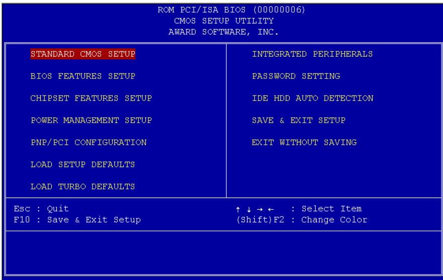

Tip: Choose "Load Setup Defaults" for recommended optimal performance. Choose "Load Turbo Defaults" for best performance with light system loading. Refer to section 3.7.
The section at the bottom of the screen tells how to control the screen. Use the arrow keys to move between items, SHIFT F2 to color scheme of the display, ESC to exit, and F10 to save the changes before exit. Another section at the bottom of the screen displays a brief description of the highlighted item.
After selecting an item, press ENTER to select or enter a submenu.
3.2 Standard CMOS Setup
The "Standard CMOS Setup" sets the basic system parameters such as the date, time, and the hard disk type. Use the arrow keys to highlight an item and PGUP or PGDN to select the value for each item.
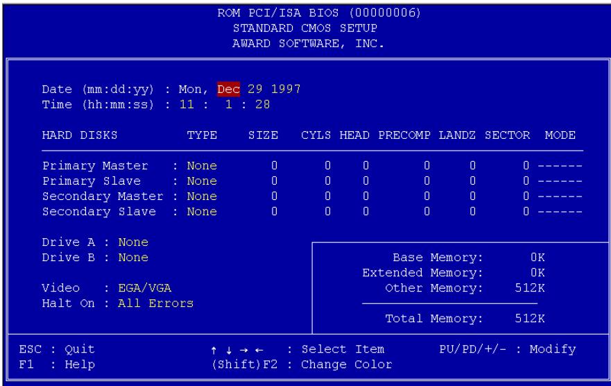
Standard CMOS Date
To set the date, highlight the Date parameter. Press PGUP or PGDN to set the current date. The date format is month, date, and year.
Standard CMOS Time
To set the time, highlight the Time parameter. Press PGUP or PCDN to set the current time in hour, minute, and second format. The time is based on the 24 hour military clock.
Standard CMOS Primary Master Type
Standard CMOS Primary Slave Type
Standard CMOS Secondary Master Type
Standard CMOS Secondary Slave Type
Type
Auto
User
None
1
2
···
45
This item lets you select the IDE hard disk parameters that your system supports. These parameters are Size, Number of Cylinder, Number of Head, Start Cylinder for Pre-compensation, Cylinder number of Head Landing Zone and Number of Sector per Track. The default setting is Auto, which enables BIOS to automatically detect the parameters of installed HDD at POST (Power-On Self Test). If you prefer to enter HDD parameters manually, select User. Select None if no HDD is connected to the system.
The IDE CDROM is always automatically detected.

Tip: For an IDE hard disk, we recommend that you use the "IDE HDD Auto Detection" to enter the drive specifications automatically. See the section "IDE HDD Auto Detection".
Standard CMOS Primary Master Mode
Standard CMOS Primary Slave Mode
Standard CMOS Secondary Master Mode
Standard CMOS Secondary Slave Mode
Mode
Auto
Normal
LBA
Large
The enhanced IDE feature allows the system to use a hard disk with a capacity of more than 528MB. This is made possible through the Logical Block Address (LBA) mode translation. The LBA is now considered as a standard feature of current IDE hard disk on the market because of its capability to support capacity larger than 528MB. Note that if HDD is formatted with LBA On, it will not be able to boot with LBA Off.
Standard CMOS Drive A
Standard CMOS Drive B
Drive A
None
360KB 5.25"
1.2MB 5.25"
720KB 3.5"
1.44MB 3.5"
2.88MB 3.5"
These items select floppy drive type. The available settings and types supported by the mainboard are listed on the left.
Standard CMOS Video
Video
EGA/VGA
CGA40
CGA80
Mono
This item specifies the type of video card in use. The default setting is VGA/EGA. Since current PCs use VGA only, this function is almost useless and may be disregarded in the future.
Standard CMOS Halt On
Halt On
No Errors
All Errors
All, But Keyboard
All, But Diskette
All, But Disk/Key
This parameter enables you to control the system stops in case of Power-On Self Test (POST) error.
3.3 BIOS Features Setup
This screen appears when you select the option "BIOS Features Setup" from the main menu.
| ROM PCI/ISA BIOS (00000007) BIOS FEATURES SETUP AWARD SOFTWARE, INC. | ||
| Virus Warning : Disabled | Video BIOS Shadow : Enabled | |
| External Cache : Enabled | C8000-CBFFF Shadow : Disabled | |
| Quick Power On Self Test : Enabled | CC000-CFFFF Shadow : Disabled | |
| Boot Sequence : A.C.SCSI | D0000-D3FFF Shadow : Disabled | |
| Swap Floppy Drive : Disabled | D4000-D7FFF Shadow : Disabled | |
| Boot Up NumLock Status : On | D8000-DBFFF Shadow : Disabled | |
| Memory Parity/ECC Check : Disabled | DC000-DFFFF Shadow : Disabled | |
| Typematic Rate Setting : Disabled | ||
| Typematic Rate (Chars/Sec) : 6 | ||
| Typematic Delay (Msec) : 250 | ||
| Security Option : Setup | ||
| IDE Second Channel Control : Enabled | Setup | |
| PCI/VGA Palette Snoop : Disabled | ||
| OS Select For DRAM > 64MB : Non-OS2 | ||
| ESC : Quit ↑↓←: Select Item | ||
| F1 : Help PU/PD/+/-: Modify | ||
| F5 : Old Values (Shift)F2 : Color | ||
| F6 : Load Setup Defaults | ||
| F7 : Load Turbo Defaults | ||
BIOS Features Virus Warning
Virus Warning
Enabled
Disabled
Set this parameter to Enabled to activate the warning message. This feature protects the boot sector and partition table of your hard disk from virus intrusion.
Any attempt during boot up to write to the boot sector of the hard disk drive stops the system and the following warning message appears on the screen. Run an anti-virus program to locate the problem.
!WARNING !
Disk Boot Sector is to be modified
Type "Y" to accept write, or "N" to abort write
Award Software, Inc.
BIOS Features External Cache
External Cache
Enabled
Disabled
Enabling this parameter activates the secondary cache (currently, PBSRAM cache). Disabling the parameter slows down the system. Therefore, we recommend that you leave it enabled unless you are troubleshooting a problem.
BIOS Features Quick Power On Self Test
Quick Power-on
Self-test
Enable
Disabled
This parameter speeds up POST by skipping some items that are normally checked.
BIOS Features Boot Sequence
Boot Sequence
A,C,SCSI
C,A,SCSI
C,CDROM,A
CDROM,C,A
D,A,SCSI
E,A,SCSI
F,A,SCSI
SCSI,A,C
SCSI,C,A
C only
LS/ZIP,C
This parameter allows you to specify the system boot up search sequence. The hard disk ID are listed below:
C: Primary master
D: Primary slave
E: Secondary master
F: Secondary slave
LS: LS120 drive
ZIP: IOMEGA ZIP drive
BIOS Features Swap Floppy Drive
Swap Floppy Drive
Enabled
Disabled
This item allows you to swap floppy drives. For example, if you have two floppy drives (A and B), you can assign the first drive as drive B and the second drive as drive A or vice-versa.
BIOS Features Boot Up NumLock Status
Boot-up NumLock Status
On
Off
Setting this parameter to On enables the numeric function of the numeric keypad. Set this parameter to Off to disregard the function. Disabling the numeric function allows you to use the numeric keypad for cursor control.
BIOS Features Memory Parity/ECC Check
Memory
Parity/ECC Check
Enabled
Disabled
This item is used to enable or disable parity/ECC check function.
BIOS Features Typematic Rate Setting
Typematic Rate Setting
Enabled
Disabled
Set this parameter to Enable/Disable the keyboard repeat function. When enabled, continually holding down a key on the keyboard will generate repeatedly keystrokes.
BIOS Features Typematic Rate (Chrs/Sec)
Typematic Rate
6
8
10
12
15
20
24
30
This item allows you to control the speed of repeated keystrokes. The default is 30 characters/sec.
BIOS Features Typematic Delay (Msec)
Typematic Delay
250
500
750
1000
This parameter allows you to control the delay time between the first and the second keystroke (where the repeated keystrokes begin). The typematic delay settings are 250, 500, 750, and 1000 msec.
BIOS Features Security Option
Security Option
Setup
System
The System option limits access to both the System boot and BIOS setup. A prompt asking you to enter your password appears on the screen every time you boot the system.
The Setup option limits access only to BIOS setup.
To disable the security option, select Password Setting from the main menu, don't type anything and just press
BIOS Features PCI/VGA Palette Snoop
PCI/VGA Palette
Snoop
Enabled
Disabled
Enabling this item informs the PCI VGA card to keep silent (and to prevent conflict) when palette register is updated (i.e., accepts data without responding any communication signals). This is useful only when two display cards use the same palette address and plugged in the PCI bus at the same time (such as MPEQ or Video capture). In such case, PCI VGA is silent while MPEQ/Video capture is set to function normally.
BIOS Features OS Select for DRAM > 64MB
OS Select for
DRAM>64MB
OS/2
Non-OS/2
Set to OS/2 if your system is utilizing an OS/2 operating system and has a memory size of more than 64 MB.
BIOS Features Video BIOS Shadow
Video BIOS
Shadow
Enabled
Disabled
VGA BIOS Shadowing means to copy video display card BIOS into the DRAM area. This enhances system performance because DRAM access time is faster than ROM.
BIOS Features C800-CBFF Shadow
BIOS Features CC00-CFFF Shadow
BIOS Features D000-D3FF Shadow
BIOS Features D400-D7FF Shadow
BIOS Features D800-DBFF Shadow
BIOS Features DC00-DFFF Shadow
C8000-CBFFF
Shadow
Enabled
Disabled
These six items are for shadowing ROM code on other expansion cards. Before you set these parameters, you need to know the specific addresses of that ROM code. If you do not know this information, enable all the ROM shadow settings.

Note: The F000 and E000 segments are always shadowed because BIOS code occupies these areas.
3.4 Chipset Features Setup
The "Chipset Features Setup" includes settings for the chipset dependent features. These features are related to system performance.
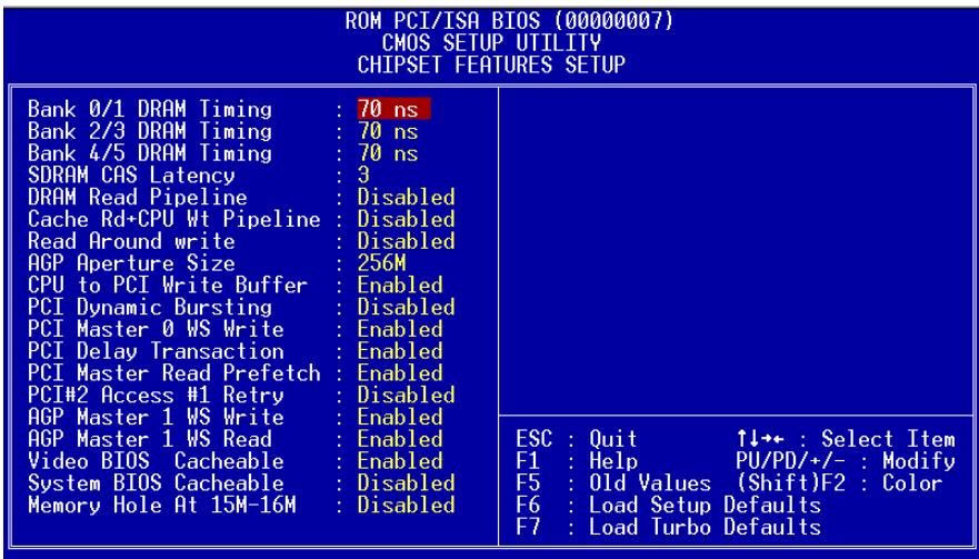

Caution: Make sure you fully understand the items contained in this menu before you try to change anything. You may change the parameter settings to improve system performance. However, it may cause system unstable if the setting are not correct for your system configuration.
Chipset Features Bank 0/1 Timing
Chipset Features Bank 2/3 Timing
Chipset Features Bank 4/5 Timing
DRAM Timing
60 ns
70 ns
This item is used to set DRAM timing parameters which can be automatically set by BIOS, 60ns and 70ns.
Chipset Features SDRAM CAS Latency
SDRAM(CAS
Lat/RAS-to-CAS)
2
3
These are timing of SDRAM CAS Latency, which is an important parameter affects SDRAM performance, default is 2 clocks. If your SDRAM has unstable problem, change 2 to 3.
Chipset Features DRAM Read Pipeline
DRAM Read Pipeline
Enabled
Disabled
This item is used to enable or disable DRAM read pipeline.
Chipset Features Cache Rd+CPU Wt Pipeline
Cache Rd+CPU Wt
Pipeline
Enabled
Disabled
This item is used to enable or disable both cache read and CPU write pipeline.
Chipset Features AGP Aperture Size
AGP Aperture Size
4M
8M
16M
32M
64M
128M
256M
This item lets you determine the effective size of the AGP Graphic Apeture.
Chipset Features CPU to PCI Write Buffer
CPU to PCI Write
Buffer
Enabled
Disabled
This item is used to enable or disable CPU to PCI write buffer.
Chipset Features PCI Dynamic Bursting
PCI Dynamic
Bursting
Enabled
Disabled
This item is used to enable or disable PCI dynamic bursting.
Chipset Features PCI Master 0 WS Write
PCI Master 0 WS
Write
Enabled
Disabled
This item is used to control the PCI master write cycle. If enabled, there is no wait state. If disabled, there will be one wait state for PCI master write.
Chipset Features PCI Delay Transaction
PCI Delay
Transaction
Enabled
Disabled
This item lets you control the Delayed Transaction function of the VIA 586A chipset (Intel PCI to ISA bridge). This function is used to meet latency of PCI cycles to or from ISA bus. Try to enable or disable it, if you have ISA card compatibility problem.
Chipset Features PCI Master Read prefetch
PCI Master Read
Prefetch
Enabled
Disabled
This item is used to control PCI master read prefetch. If enabled, chipset will do prefetch only if enhanced command. If disabled, it will be always prefetch.
Chipset Features PCI#2 Access #1 Retry
PCI#2 Access #1
Retry
Enabled
Disabled
This item is used to enable or disable AGP master retry disconnect. If enabled, AGP master will be disconnected if max retries are attempted without success. PCI#2 means AGP.
Chipset Features AGP Master 1 WS Write
AGP Master 1 WS Write
Enabled
Disabled
This item is used to enable or disable AGP master 1 wait state write.
Chipset Features AGP Master 1 WS Read
AGP Master 1 WS Read
Enabled
Disabled
This item is used to enable or disable AGP master 1 wait state read.
Chipset Features Video BIOS Cacheable
Video BIOS Cacheable
Enabled
Disabled
Allows the video BIOS to be cached to allow faster video performance.
Chipset Features System BIOS Cacheable
System BIOS Cacheable
Enabled
Disabled
Enabling this item allows you to cache the system BIOS to further enhance system performance.
Chipset Features Memory Hole At 15M-16M
Memory Hole At 15M-16M
Enabled
Disabled
This option lets you reserve system memory area for special ISA cards. The chipset accesses code/data of these areas from the ISA bus directly. Normally, these areas are reserved for memory mapped I/O card.
3.5 Power Management Setup
The Power Management Setup screen enables you to control the mainboard's green features. See the following screen.
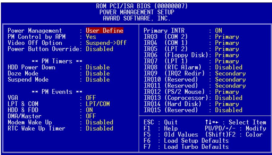
Power Management Power Management
Power Management
Max Saving
Mix Saving
User Defined
Disabled
This function allows you to set the default parameters of power-saving modes. Set to Disable to turn off power management function. Set to User Defined to choose your own parameters.
| Mode | Doze | Standby | Suspend | HDD Power Down |
| Min Saving | 1 hour | 1 hour | 1 hour | 15 min |
| Max Saving | 1 min | 1 min | 1 min | 1 min |
Power Management PM Controlled by APM
PM Controlled by APM
Yes
No
If "Max Saving" is selected, you can turn on this item, transfer power management control to APM (Advanced Power Management) and enhance power saving function. For example, stop CPU internal clock.
Power Management Video Off Option
Video Off Option
Always On
All Modes Off
Suspend Off
Susp, Standby Off
To turn off video monitor at which power down mode.
Power Management Power Button Override
Power Button Override
Enabled
Disabled
This is a specification of ACPI and supported by hardware. When Enabled, the soft power switch on the front panel can be used to control power On, Suspend and Off. If the switch is pressed less than 4 sec during power On, the system will go into Suspend mode. If the switch is pressed longer than 4 sec, the system will be turned Off. The default setting is Disabled, soft power switch is only used to control On and Off, there is no need to press 4 sec, and there is no Suspend.
Power Management HDD Power Down
HDD Power Down
Disabled
1 Min
···
15 Min
This option lets you specify the IDE HDD idle time before the device enters the power down state. This item is independent from the power states previously described in this section (Standby and Suspend).
Power Management Doze Mode
Doze Mode
Disabled
1 Min
2 Min
4 Min
8 Min
12 Min
20 Min
30 Min
40 Min
1 Hour
This item lets you set the period of time after which the system enters into Doze mode. In this mode, the CPU clock slows down. The ratio is specified in the "Throttle Duty Cycle". Any activity detected returns the system to full power. The system activity (or event) is detected by monitoring the IRQ signals.
Power Management Suspend Mode
Suspend Mode
Disabled
1 Min
2 Min
4 Min
8 Min
12 Min
20 Min
30 Min
40 Min
1 Hour
This item lets you set the period of time after which the system enters into Suspend mode. The Suspend mode can be Power On Suspend or Suspend to Hard Drive, selected by "Suspend Mode Option".
Power Management VGA
Power Management LPT & COM
Power Management HDD & FDD
Power Management DMA/Master
COM Ports Activity
ON
OFF
To enable or disable the detection of COM port, LPT, HDD, VGA, and DMA activities for power down state transition.
Power Management Modem Wake Up
Modem Wake Up
Disabled
Enabled
This motherboard implements AOpen special circuit to detect modem ring signal and wakeup from soft power off. The most possible applications are automatic answering machine and fax send/receive. It does not like traditional green PC suspend mode, the system can be true power off, (identified by the fan of your power supply is off). You can use external box modem or AOpen MP56/F56 internal modem card for modem ring-on, but MP56/F56 is recommended, since MP56/F56 has special circuit to cooperate with this mainboard and the modem power and system power can be off together.
Power Management RTC Wake Up Timer
RTC Wake Up Timer
Enabled
Disabled
This option lets you enable or disable the RTC Wake Up function.
Power Management WakeUp Date (of Month)
WakeUp Date (of Month)
0
1
···
31
This item is displayed when you enable the RTC Wake Up Timer option. Here you can specify what date you want to wake up the system. For Example, setting to 15 will wake up the system on the 15th day of every month.

Note: Setting this item to 0 will wake up the system on the specified time (which can be set in the WakeUp Time item) every day.
Power Management WakeUp Time (hh:mm:ss)
WakeUp Time (hh:mm:ss)
hh:mm:ss
This item is displayed when you enable the RTC Wake Up Timer option. Here you can specify what time you want to wake up the system.
Power Management Primary INTR
Primary
ON
OFF
This item is used to enable or disable the detection of IRQ3-15 or NMI interrupt events for power down state transition. Normally, this is applied to network card.
Power Management IRQ [3-15]
IRQ [3-15],NMI
Primary
Secondary
Disabled
Select Primary or Disabled option to enable or disable the detection of specified IRQ. If the Secondary option was selected, the system will wake up for 2ms after detecting the interrupt, and then return to power down status.
3.6 PNP/PCI Configuration Setup
The PNP/PCI Configuration Setup allows you to configure the ISA and PCI devices installed in your system. The following screen appears if you select the option "PNP/PCI Configuration Setup" from the main menu.
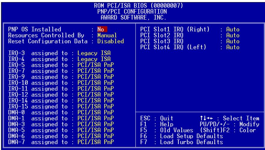
PNP/PCI Configuration PnP OS Installed
PnP OS Installed
Yes
No
Normally, the PnP resources are allocated by BIOS during POST (Power-On Self Test). If you are using a PnP operating system (such as Windows 95), set this item to Yes to inform BIOS to configure only the resources needed for booting (VGA/IDE or SCSI). The rest of system resources will be allocated by PnP operating system.
PNP/PCI Configuration Resources Controlled By
Resources Controlled by
Auto
Manual
Setting this option to Manual allows you to individually assign the IRQs and DMAs to the ISA and PCI devices. Set this to Auto to enable the auto-configuration function.
PNP/PCI Configuration Reset Configuration Data
Reset Configuration
Data
Enabled
Disabled
In case conflict occurs after you assign the IRQs or after you configure your system, you can enable this function, allow your system to automatically reset your configuration and reassign the IRQs.
PNP/PCI Configuration IRQ3 (COM2)
PNP/PCI Configuration IRQ4 (COM1)
PNP/PCI Configuration IRQ5 (Network/Sound or Others)
PNP/PCI Configuration IRQ7 (Printer or Others)
PNP/PCI Configuration IRQ9 (Video or Others)
PNP/PCI Configuration IRQ10 (SCSI or Others)
PNP/PCI Configuration IRQ11 (SCSI or Others)
PNP/PCI Configuration IRQ12 (PS/2 Mouse)
PNP/PCI Configuration IRQ14 (IDE1)
PNP/PCI Configuration IRQ15 (IDE2)
IRQ3
Legacy ISA
PCI/ISA PnP
If your ISA card is not PnP compatible and requires a special IRQ to support its function, set the selected IRQ to Legacy ISA. This setting informs the PnP BIOS to reserve the selected IRQ for the installed legacy ISA card. The default is PCI/ISA PnP. Take note that PCI cards are always PnP compatible (except old PCI IDE card).
PNP/PCI Configuration DMA 0
PNP/PCI Configuration DMA 1
PNP/PCI Configuration DMA 3
PNP/PCI Configuration DMA 5
PNP/PCI Configuration DMA 6
PNP/PCI Configuration DMA 7
DMA 0
Legacy ISA
PCI/ISA PnP
If your ISA card is not PnP compatible and requires a special DMA channel to support its function, set the selected DMA channel to Legacy ISA. This setting informs the PnP BIOS to reserve the selected DMA channel for the installed legacy ISA card. The default is PCI/ISA PnP. Take note that PCI card does not require DMA channel.
PNP/PCI Configuration PCI Slot1 IRQ (Right)
PNP/PCI Configuration PCI Slot2 IRQ
PNP/PCI Configuration PCI Slot3 IRQ
PNP/PCI Configuration PCI Slot4 IRQ (Left)
PCI Slot1 IRQ
3
4
5
7
9
10
11
12
14
15
Auto
This item is reserved for engineering purpose to let you assign an IRQ manually to the add-on card on each PCI slot. If you select Auto, system will automatically assign an available value to the device.
It is suggested to use default setting, which is Auto, in order to comply with PnP specification completely.
3.7 Load Setup Defaults
The "Load Setup Defaults" option loads optimized settings for optimum system performance. Optimal settings are relatively safer than the Turbo settings. We recommend you to use the Optimal settings if your system has large memory size and fully loaded with add-on card (for example, a file server using double-sided 8MB SIMM x4 and SCSI plus Network card occupying the PCI and ISA slots).
Optimal is not the slowest setting for this mainboard. If you need to verify a unstable problem, you may manually set the parameter in the "BIOS Features Setup" and "Chipset Features Setup" to get slowest and safer setting.
3.8 Load Turbo Defaults
The "Load Turbo Defaults" option gives better performance than Optimal values. However, Turbo values may not be the best setting of this mainboard but these values are qualified by the AOpen RD and QA department as the reliable settings especially if you have limited loading of add-on card and memory size (for example, a system that contains only a VGA/Sound card and two SIMMs).
To attain the best system performance, you may manually set the parameters in the "Chipset Features Setup" to get proprietary setting. Make sure that you know and understand the functions of every item in Chipset Setup menu. The performance difference of Turbo from Optimal is normally around 3% to 10% , depending on the chipset and the application.
3.9 Integrated Peripherals
The following screen appears if you select the option "Integrated Peripherals" from the main menu. This option allows you to configure the I/O features.
| ROM PCI/ISA BIOS (00000007) INTEGRATED PERIPHERALS AWARD SOFTWARE, INC. | ||
| OnChip IDE First Channel: Enabled OnChip IDE Second Channel: Enabled IDE Prefetch Mode: Disabled IDE HDD Block Mode: Enabled IDE Primary Master PIO: Auto IDE Primary Slave PIO: Auto IDE Secondary Master PIO: Auto IDE Secondary Slave PIO: Auto IDE Primary Slave UDMA: Auto IDE Primary Slave UDMA: Auto IDE Secondary Master UDMA: Auto IDE Secondary Slave UDMA: Auto USB Controller: Disabled | Onboard Parallel Mode: SPP | |
| Onboard FDD Controller: Enabled Onboard Serial Port 1: 3F8/IRQ4 Onboard Serial Port 2: 2F8/IRQ3 Onboard UART 2 Mode: Standard Onboard Parallel Port: 378/IRQ7 | ESC: Quit ↑↓++: Select Item F1: Help PU/PD+/+/-: Modify F5: Old Values (Shift)F2: Color F6: Load Setup Defaults F7: Load Turbo Defaults | |
Integrated Peripherals OnChip IDE First Channel Integrated Peripherals OnChip IDE Second Channel
OnChip IDE First
Channel
Enabled
Disabled
This parameter lets you enable or disable the IDE device connected to the primary IDE connector.
Integrated Peripherals IDE Prefixch Mode
IDE Prefetch Mode
Enabled
Disabled
This item is used to enable and disable IDE prefetch mode.
Integrated Peripherals IDE HDD Block Mode
IDE HDD Block
Mode
Enabled
Disabled
This feature enhances disk performance by allowing multisector data transfers and eliminates the interrupt handling time for each sector. Most IDE drives, except with old designs, can support this feature.
Integrated Peripherals IDE Primary Master PIO Integrated Peripherals IDE Primary Slave PIO Integrated Peripherals IDE Secondary Master PIO Integrated Peripherals IDE Secondary Slave PIO
IDE Primary Master
PIO
Auto
Mode 1
Mode 2
Mode 3
Mode 4
Setting this item to Auto activates the HDD speed auto-detect function. The PIO mode specifies the data transfer rate of HDD. For example: mode 0 data transfer rate is 3.3MB / s , mode 1 is 5.2MB / s , mode 2 is 8.3MB / s , mode 3 is 11.1MB / s and mode 4 is 16.6MB / s . If your hard disk performance becomes unstable, you may manually try the slower mode.

Caution: It is recommended that you connect the first IDE device of each channel to the endmost connector of the IDE cable. Refer to section 2.3 "Connectors" for details on how to connect IDE device(s).
Integrated Peripherals IDE Primary Master UDMA Integrated Peripherals IDE Primary Slave UDMA Integrated Peripherals IDE Secondary Master UDMA Integrated Peripherals IDE Secondary Slave UDMA
IDE Primary Master
UDMA
Auto
Disabled
This item allows you to set the Ultra DMA/33 mode supported by the hard disk drive connected to your primary IDE connector.
Integrated Peripherals USB Controller
USB Controller
Enabled
Disabled
This item is used to enable or disable USB controller.
Integrated Peripherals USB Legacy Support
USB Legacy Support
Enabled
Disabled
This item lets you enable or disable the USB keyboard driver within the onboard BIOS. The keyboard driver simulates legacy keyboard command and let you use USB keyboard during POST or after boot if you don't have USB driver in the operating system.

Caution: You can not use both USB driver and USB legacy keyboard at the same time. Disable "USB Legacy Support" if you have USB driver in the operating system.
Integrated Peripherals Onboard FDC Controller
Onboard FDC
Controller
Enabled
Disabled
Setting this parameter to Enabled allows you to connect your floppy disk drives to the onboard floppy disk connector instead of a separate controller card. Change the setting to Disabled if you want to use a separate controller card.
Integrated Peripherals Onboard Serial Port 1 Integrated Peripherals Onboard Serial Port 2
Onboard Serial Port 1
Auto
3F8/IRQ4
2F8/IRQ3
3E8/IRQ4
2E8/IRQ3
Disabled
This item allows you to assign address and interrupt for the board serial port. Default is Auto.

Note: If you are using an network card, make sure that the interrupt does not conflict.
Integrated Peripherals Onboard UART 2 Mode
Onboard UART 2
Mode
Standard
HPSIR
ASKIR
This item is configurable only if the "Onboard UART 2" is enabled. This allows you to specify the mode of serial port2. The available mode selections are:
- Standard - Sets serial port 2 to operate in normal mode. This is the default setting.
- HPSIR - Select this setting if you installed an Infrared module in your system via IrDA connector (refer to section 2.3 "Connectors"). This setting allows infrared serial communication at a maximum baud rate of 115K baud.
- ASKIR - Select this setting if you installed an Infrared module via IrDA connector (refer to section 2.3 "Connectors"). This setting allows infrared serial communication at a maximum baud rate of 19.2K baud.
Integrated Peripherals Onboard Parallel Port
Onboard Parallel
Port
3BC/IRQ7
378/IRQ7
278/IRQ7
Disabled
This item controls the onboard parallel port address and interrupt.

Note: If you are using an I/O card with a parallel port, make sure that the addresses and IRQ do not conflict.
Integrated Peripherals Parallel Port Mode
Parallel Port Mode
Normal
SPP
EPP 1.7 + SPP
EPP 1.9 + SPP
ECP
EPP 1.7 + ECP
EPP 1.9 + ECP
This item lets you set the parallel port mode. The mode options are Normal (Standard and Bidirection Parallel Port), EPP (Enhanced Parallel Port) and ECP (Extended Parallel Port). Normal is the IBM AT and PS/2 compatible mode. EPP enhances the parallel port throughput by directly writing/reading data to/from parallel port without latch. ECP supports DMA and RLE (Run Length Encoded) compression and decompression. EPP1.7 and EPP1.9 are protocol difference.
Integrated Peripherals ECP Mode Use DMA
ECP Mode Use DMA
3
1
This item lets you set the DMA channel of ECP mode.
3.10 Password Setting
Password prevents unauthorized use of your computer. If you set a password, the system prompts for the correct password before boot or access to Setup.
To set a password:
- At the prompt, type your password. Your password can be up to 8 alphanumeric characters. When you type the characters, they appear as asterisks on the password screen box.
- After typing the password, press.
- At the next prompt, re-type your password and press again to confirm the new password. After the password entry, the screen automatically reverts to the main screen.
To disable the password, press when prompted to enter the password. The screen displays a message confirming that the password has been disabled.
3.11 IDE HDD Auto Detection
If your system has an IDE hard drive, you can use this function to detect its parameters and enter them into the "Standard CMOS Setup" automatically.
This routine only detects one set of parameters for your IDE hard drive. Some IDE drives can use more than one set of parameters. If your hard disk is formatted using different parameters than those detected, you have to enter the parameters manually. If the parameters listed do not match the ones used to format the disk, the information on that disk will not be accessible. If the auto-detected parameters displayed do not match those that used for your drive, ignore them. Type N to reject the values and enter the correct ones manually from the Standard CMOS Setup screen.
3.12 Save & Exit Setup
This function automatically saves all CMOS values before leaving Setup.
3.13 Exit without Saving
Use this function to exit Setup without saving the CMOS value changes. Do not use this option if you want to save the new configuration.
3.14 NCR SCSI BIOS and Drivers
The NCR 53C810 SCSI BIOS resides in the same flash memory chip as the system BIOS. The onboard NCR SCSI BIOS is used to support NCR 53C810 SCSI control card without BIOS code.
The NCR SCSI BIOS directly supports DOS, Windows 3.1 and OS/2. For better system performance, you may use the drivers that come with the NCR SCSI card or with your operating system. For details, refer to the installation manual of your NCR 53C810 SCSI card.
3.15 BIOS Flash Utility
The BIOS Flash utility allows you to upgrade the system BIOS. To get the AOpen Flash utility and the upgrade BIOS file, contact your local distributor or visit our homepage at http://www.aopen.com.tw. Please make sure that you have the correct BIOS ready, the BIOS filename is normally like AP5TR110.BIN, which means model AP5T BIOS revision 1.10.
There are two useful programs, Checksum utility CHECKSUM.EXE and AOpen Flash utility AOFLASH.EXE. Follow the procedures below to upgrade your BIOS.
[CHECKSUM.EXE]
This utility will help you to determine if the BIOS has been downloaded correctly or not.
- Execute
C: CHECKSUM Biosfile.bin
Biosfile.bin is the filename of the BIOS code.
-
The utility will show "Checksum is ssss".
-
Compare the "sss" with original checksum posted on Web or BBS. If they are different, please do not proceed any further and try to download the BIOS again.
[AOFLASH.EXE]
This utility will try to check the mainboard model, BIOS version and Super/Ultra IO chip model. To ensure the correct BIOS file for the correct mainboard and IO chip. This utility will permanently replace your original BIOS content after flashing.
- Bootup the system from DOS prompt without loading any memory manager (HIMEM, EMM386, QEMM386, ...).
- Execute
C:> AOFLASH Biosfile.bin
Biosfile.bin is the filename of the BIOS code.
- After loading the new BIOS code, the utility will prompt you to save original BIOS code into your HDD or floppy. Please press "Y" to store it as "BIOS.OLD".
- After the old BIOS has been successfully saved, press "Y" to replace BIOS.
- DO NOT turn off the power during "FLASHING".
- Reboot the system by turn off the power after "FLASHING".
- Press "DEL" key to enter BIOS setup during POST.
- Reload the "BIOS SETUP DEFAULT" and reconfigure other items as previous set.
- Save & Exit. Done!
![AOPEN AX59PRO - [AOFLASH.EXE] - 1](/content/2025/01/184076/images/ee7bb4d55bbc3bf418984d6ae0c8d3ec7757b34f6aba02a9339b726cc160a6fa.jpg)
Warning: DO NOT turn off the power during "FLASHING". If the BIOS programming is not successfully finished, the system will not be boot again, and you may need to physically replace the BIOS chip.
![AOPEN AX59PRO - [AOFLASH.EXE] - 2](/content/2025/01/184076/images/0da83008e71a3661c302a6ad46744810fcf27c9590a595a0377e1498b3958cc2.jpg)
Tip: You may load back original BIOS "BIOS.OLD" by the same procedure.
Appendix A
Frequently Asked Question

Note: FAQ may be updated without notice. If you cannot find the information that you need in this appendix, visit our WWW home page, (address: http://www.aopen.com.tw) and check the FAQ area and other new information.
Q: How can I identify the mainboard BIOS version?
A: The AOpen mainboard BIOS version appears on the upper-left corner of the POST (Power-On Self Test) screen. Normally, it starts with R and is found in between the model name and the date. For example:

Q: How can I identify the model name & revision of the mainboard from PCB?
A: The AOpen mainboard revision appears as REV:X.X on the PCB, usually it is under beneath of AOpen Logo & mainboard model name. For example, "AX6L REV:1.2" shall appear on the PCB as follows:

AX6L
REV:1.2
Q: What is MMX?
A: MMX is the new single-line multiple-instruction technology of the new Intel Pentium PP/MT (P55C) and Pentium II (Klamath) CPU. The AMD K6 and Cyrix M2 will support MMX, too. The MMX instructions are specifically useful for multimedia applications (such as 3D video, 3D sound, video conference). The performance can be improved if applications use these instructions. All AOpen MBs have at least dual power onboard to support MMX. It is not necessary to have special chipset for MMX CPU.
Q: What is USB (Universal Serial Bus)?
A: USB is a new 4-pin serial peripheral bus that is capable of cascading low/medium speed peripherals (less than 10Mbit/s) such as keyboard, mouse, joystick, scanner, printer and modem/ISDN. With USB, the traditional complex cables from back panel of your PC can be eliminated.
You need the USB driver to support USB device(s). AOpen MBs are all USB ready, you may get latest BIOS from AOpen web site (http://www.aopen.com.tw). Our latest BIOS includes the keyboard driver (called Legacy mode), that simulates USB keyboard to act as AT or PS/2 keyboard and makes it possible to use USB keyboard if you don't have driver in your OS. For other USB devices, you may get the drivers from your device vendor or from OS (such as Win95). Be sure to turn off "USB Legacy Support" in BIOS "Chipset Setup" if you have another driver in your OS.
Q: What is FCC DoC (Declaration of Conformity)?
A: The DoC is new certification standard of FCC regulations. This new standard allows DIY component (such as mainboard) to apply DoC label separately without a shielding of housing. The rule to test mainboard for DoC is to remove housing and test it with regulation 47 CFR 15.31. The DoC test of mainboard is more difficult than traditional FCC test. If the mainboard passes DoC test, that means it has very low EMI radiation and you can use any kind of housing (even paper housing). Following is an example of DoC label.

Q: What is Bus Master IDE (DMA mode)?
A: The traditional PIO (Programmable I/O) IDE requires the CPU to involve in all the activities of the IDE access including waiting for the mechanical events. To reduce the workload of the CPU, the bus master IDE device transfers data from/to memory without interrupting CPU, and releases CPU to operate concurrently while data is transferring between memory and IDE device. You need the bus master IDE driver and the bus master IDE HDD to support bus master IDE mode. Note that it is different with master/slave mode of the IDE device connection. For more details, refer to section 2.3 "Connectors".
Q: What is the Ultra DMA/33?
A: This is the new specification to improve IDE HDD data transfer rate. Unlike traditional PIO mode, which only uses the rising edge of IDE command signal to transfer data, the DMA/33 uses both rising edge and falling edge. Hence, the data transfer rate is double of the PIO mode 4 or DMA mode 2. (16.6MB/s x2 = 33MB/s).
The following table lists the transfer rate of IDE PIO and DMA modes. The IDE bus is 16-bit, which means every transfer is two bytes.
| Mode | Clock per 33MHz PCI | Clock count | Cycle time | Data Transfer rate |
| PIO mode 0 | 30ns | 20 | 600ns | (1/600ns) x 2byte = 3.3MB/s |
| PIO mode 1 | 30ns | 13 | 383ns | (1/383ns) x 2byte = 5.2MB/s |
| PIO mode 2 | 30ns | 8 | 240ns | (1/240ns) x 2byte = 8.3MB/s |
| PIO mode 3 | 30ns | 6 | 180ns | (1/180ns) x 2byte = 11.1MB/s |
| PIO mode 4 | 30ns | 4 | 120ns | (1/120ns) x 2byte = 16.6MB/s |
| DMA mode 0 | 30ns | 16 | 480ns | (1/480ns) x 2byte = 4.16MB/s |
| DMA mode 1 | 30ns | 5 | 150ns | (1/150ns) x 2byte = 13.3MB/s |
| DMA mode 2 | 30ns | 4 | 120ns | (1/120ns) x 2byte = 16.6MB/s |
| DMA/33 | 30ns | 4 | 120ns | (1/120ns) x 2byte x2 = 33MB/s |
Q: What is ACPI (Advanced Configuration & Power Interface) and OnNow?
A: The ACPI is new power management specification of 1997 (PC97). It intends to save more power by taking full control of power management to operating system and not through BIOS. Because of this, the chipset or super I/O chip needs to provide standard register interface to OS (such as Win97) and provides the ability for OS to shutdown and resume power of different part of chip. The idea is a bit similar to the PnP register interface.
ACPI defines momentary soft power switch to control the power state transition. Most likely, it uses the ATX form factor with momentary soft power switch. The most attractive part of ACPI for desktop user is probably the "OnNow" feature, an idea from notebook. This feature allows you to immediately resume to your original work without the long time waiting from bootup, entering Win95 and running Winword.
Q: What is ATX Soft Power On/Off and Momentary Switch?
A: The Soft Power On of the ATX specification means to provide a standby current for special circuit to wait for wakeup event when main power is off. For example, Infrared wakeup, modem wakeup, or voice wakeup. Currently, the most simple usage is to provide standby current for power switch circuit so that power switch can turn on/off the main power through soft power control pin. The ATX power specification does not mention anything about the power switch type. You can use toggle or momentary switch, note that ACPI specification requires momentary switch for power state control. All the AOpen ATX MBs support momentary switch and AX5T/AX5TC/AX6L/AX6LC/ AX6B/AX6BC support modem wakeup (Modem Ring-On).
Soft Power Off means to turn off system through software, Windows 95 Shutdown function can be used to verify if your mainboard supports soft power off. AOpen AX5T/AX5TC/AX6F/AX6L/AX6LC/AX6BAX6BC support soft power off.
Q: What is RTC Wake Up Timer (Alarm)?
A: RTC (Real Time Clock) is a device like electronic watch, and keep the date/time of the computer system running. The Wake Up Timer is more like an alarm, which wakes up and powers on your system at a pre-defined time for specific application. It can be set to wake up everyday or on specific date within a month. The date/time accurate is second. To set the date/time, go into BIOS setup, Power Management RTC Wake Up Timer, select Enable. RTC is a standard device of all the mainboard, but Wake Up Timer is not a standard design, AOpen AX5T/AX59Pro/AX5TC/AX6F/AX6L/AX6LC/AX6B /AX6BC support RTC Wake Up Timer.
Q: What is Lan Wake Up?
A: Lan Wake Up is a technology that enables you to remotely manage the PCs in your network even if they have been turned off. When the client has been powered off, the remote network management software could send a wake-up frame ( or Magic packet) to the client if needed. The Lan Wake Up enabled adapter in the client will receive that frame can check it to determine whether the frame contains the correct MAC address. If so, the client turns on the system by Wake-up call, just as the user turns on the system manually with
the ON/OFF button. The network management software will continue to perform the tasks that have been programmed to do.
Q: What is the AGP (Accelerated Graphic Port)?
A: AGP is a PCI-like bus interface targeted for high-performance 3D graphic. AGP supports only memory read/write operation and single-master single-slave one-to-one only. The AGP uses both rising and falling edge of the 66MHz clock and produces 66MHz x 4byte x 2 = 528MB/s data transfer rate. The AOpen AX6L and AX6B MB are designed to support AGP via the new Intel LX & BX chipset.
Q: Why is there a resource conflict between my AGP VGA card & PCI-to-PCI bridge (or AGP bridge) within Device Manger under Windows '95?
A: It is normal for AGP cards to conflict with the PCI standard PCI-to-PCI bridge (or AGP bridge). Since Windows'95 does not inherently support AGP technology, it reports this conflict incorrectly. This conflict will not adversely affect the performance of your system. Attempting to resolve it will result in improper operation of the PC. This issue is expected to be fixed by Microsoft when Windows 98 released.
Q: Power Management Icon does not appear in the Windows 95 Control Panel even though the APM under BIOS Setup is enabled.
A: This problem occurs if you did not enable the APM function before you install Windows 95. If you have already installed Windows 95, re-install it after the BIOS APM function is enabled.
Q: Which version of the Windows '95 that I am using?
A: You may determine the version of Windows '95 by following steps.
- Double click "System" in "Control Panel".
- Click "General".
- Look for "System" heading & refer to following,
4.00.950 Windows 95
4.00.950A Windows 95 + Service Pack or OEM Service Release 1
4.00.950B OEM Service Release 2 or OEM Service Release 2.1
4.00.950C OEM Service Release 2.5
If you are running OSR 2.1, you may tell it from by checking "USB Supplement to OSR2" in the list of installed program of Add/Remove program tool under Control Panel, and checking for version 4.03.1212 of the Ntkern.vxd file in the Windows\System\Vmm32 folder.
Q: How can I eliminate the "?" marks presented under Device Manager after installing Win'95 on TX/LX/BX/MVP3/5591 based system?
A: Even though your system will work fine with this "?" marks, we received many requests about how to eliminate it. AOpen software team spends few weeks to develop an utility AOchip.exe for the convenience of Win95 users. It is very user friendly and can be used on any TX/LX/BX/MVP3/5591 chipset based motherboard, not limited to AOopen products. You are welcome to distribute it, if you like it, simply say thanks to our software team. Note that you need USB driver for USB devices to work properly which is expected to be implemented on Windows'98.
Q: What is LDCM (LAN Desktop Client Manager)?
A: This is a software of Intel. The major goal is to provide an easy way for corporate network administrator to monitor the status of all the clients (workstation). You need at least DMI BIOS for LDCM. AOpen BIOS is also DMI ready but unfortunately, Intel LDCM needs Intel network card and ATI VGA to work properly. It is obviously not suitable for home user to pay LDCM extra cost.
Q: How to install Windows 95 USB driver?
A: If you are Win'95 OSR 2.0 user (.950B, shows "PCI Universal Serial Devices"), you may obtain USBSUPP.EXE from Microsoft or your OEM system provider for installing Microsoft USB supplement which will create "USB Supplement to OSR2" in the list of Add/Remove program tool under Control Panel. After above installation, please run AOchip.exe provided by AOpen to create USB Controller under Device Manager.
If you are Win'95 OSR 2.1 or 2.5 user, only AOchip.exe installation is necessary.
If you are Win'95 retail user (.950 or .950A), there is no direct upgrade path available from Microsoft at this moment. It is expected to be implemented under Windows'98.
Q: What is the benefit of using Resettable Fuse?
A: The traditional pico-fuse needs to be replaced once it is burned due to any abnormal surge current. It has to be replaced by qualified repairing engineer which is cost & time consuming. With the updated technology, AOpen motherboard starts to introduce new "Resetable" fuse, which is "PolySwitch", to protect your keyboard & USB circuit. When there is surge current, this PolySwitch will reach high impedance within few m/seconds so that the circuit
becomes opened. PolySwitch will be recovered to its original stage after surge current disappeared & the system is being cooled down for a while.
It is highly recommended to adopt "Resetable" fuse in order to fully support "Hot-Plug" feature on USB.
Q: What is Hardware Monitoring?
A: There are four high-valued "Hardware Monitoring" features being implemented on AOpen ATX mainboard.
- Over Current Protection: Providing over current protection for CPU Vcore. In conjunction with the over current protection provided by ATX power supply on 3.3V/5V/12V, it gives the full line over current protection.
- System Voltage Monitoring: As you turn your system on, this smart design will continue to monitor your system working voltage. If any of the system voltage is over the component's standard, there will be warning alarm from PC speaker when AOHW100 or ADM installed.
- Thermal Protection: The higher speed of CPU, the more heat dissipation ability is needed to be taken into consideration. If user does not use a correct fan for the CPU cooling, it is highly possible the CPU will be overheating and cause system unstable. AOpen mainboard monitors CPU & System temperatures by using two thermal sensors.
- Fan Monitoring: There are two three-pin fan connectors, one is for CPU and the other one can be connected to the housing fan. The system will report the rotational speed of the fan and alarm fan malfunction though utility software such as AOHW100 or ADM.
Q: What is AOHW100 (Hardware Monitoring Utility)?
A: This is the Hardware Monitoring Utility software (AOHW100) developed by AOpen which monitors the status of system voltage, thermal, & fan. Instead of using ADM or LDCM which supports network administration, AOHW100 is especially designed for personal user. You may install it on your AOpen mainboard based system which comes with Hardware Monitoring features.
Q: What is ADM (Advanced Desktop Manager)?
A: This is a desktop client and server management software developed by AOpen. It is similar as Intel LDCM with some improvement. ADM is not only for corporate network management, it can also be used as system status monitoring utility, for example, CPU fan, thermal and system voltage monitoring.
| Features | ADM 2.0 | LDCM 3.0 |
| VGA card | No limitation | Only ATI |
| Network card | No limitation | Only Intel |
| Support DMI BIOS 2.0 | Yes | Yes |
| Support Win95 | Yes | Yes |
| Support Win NT | No (will be supported on ADM 2.1) | Yes |
| Real-Time CPU/Memory Utilization Monitoring | Yes | No |
| Multi-Machine Monitoring on One Screen | Yes | No |
| Remote Management Protocol | Standard SNMP protocol | Intel proprietary RAP protocol |
| Standard SNMP Trap | Yes (so that can work with standard software such as HP Open View) | No |
| Remote File Transfer | No | Yes |
Q: Why do AOpen MBs use many Electrolytic Capacitors instead of Tantalum Capacitor?
A: The quality of Electrolytic capacitor has huge difference depends on model and vendor. Normally, Tantalum capacitor is better than Electrolytic capacitor, but good quality and high price Electrolytic capacitor is even better than Tantalum capacitor. Originally, AOpen motherboards use 100uF Tantalum capacitor nears CPU to reduce voltage ripple, but the technology improvement has introduced an 1000uF very low ESR (Equivalent Serial Resistor) of Electrolytic capacitor with only 0.15 ohm comparing with 0.7 ohm of Tantalum capacitor. The lower the ESR and higher the capacitance value, the smaller the CPU voltage ripple.
Following are the specifications of capacitors that AOpen is currently using:
Tantalum: SPRAGUE 100uF,
Part number 595D107X06R3C2T,
Max ESR is 0.7 at 25 degree 100kHz
Electrolytic: SANYO 1000uF,
Part number 16MV1000CG,
Max ESR is 0.15 at 20 degree 100khz.
Also, more capacitors are not exactly equal to better CPU voltage, it depends on where you put your capacitor (the layout). The most accurate way is to use storage scope to measure the CPU voltage directly, but of course, it is difficult for end user to do so. AOpen design team follows Intel, AMD and Cyrix's design specification strictly, it is approved by Intel, AMD and Cyrix.
Q: What is PC 100 SDRAM?
A: It's apparent that traditional FPM and EDO DRAMs won't be able to work properly under 100MHz system clock frequency. In order to fully support 100MHz or even above bus clock system, Intel provided PC SDRAM Specifications to facilitate the development of SDRAM products. This is also known as PC 100 SDRAM specification. For getting the best performance and stability under 100MHz or above external clock, we strongly recommend you use the Synchronous DRAMs which meet the PC 100 requirement. The PC 100 SDRAM that AOpen QA Team had tested are listed below.
| Size | Vendor | Model | Single/Double | Chip Count |
| 16M | Hyundai | HY57V168010CTC-10 | x1 | 8 |
| 32M | NEC | D4516821AG5-A10-7JF | x1 | 16 |
| 32M | SEC | KM48S2020CT-GH | x2 | 18 |
| 32M | Hyundai | HY57V168010CTC-10 | x2 | 16 |
| 32M | Micron | MT48LC2M8A1-08 | x2 | 16 |
| 32M | Fujitsu | 81F16822D-A10-7JF | x2 | 18 |
| 64M | Mitsubishi | M5M4V64S30ATP -10 | x1 | 9 |
| 64M | Fujitsu | 81F64842B-103FN | x1 | 9 |
| 64M | NEC | D4564841G5-A10-9JF | x1 | 9 |
| 64M | SEC | KM48S8030BT-GH | x1 | 9 |
| 64M | Toshiba | TC59S6408FTL-80H | x1 | 9 |
Appendix B
Troubleshooting
In case you encounter any of the troubles listed below, follow the procedures accordingly to resolve the problem. If the first corrective action listed did not work, then try the next one.

Tip: There are many useful information in our homepage, such as jumper settings, latest BIOS, drivers, and more FAQs. Visit our homepage to see if there is an answer of your problem.
Taiwan http://www.aopen.com.tw
USA http://www.aopen-usa.com
http://www.aopenamerica.com
Europe http://www.aopen.nl

Important: Make sure that you have tried listed procedures in this appendix before you call your distributor. If the problem still exist, fill out the attached Technical Problem Report Form. Please write down your configuration and error symptoms as detailed as possible. The more detailed information you give us, the faster we can identify and solve your problem. You can copy this form and fax it to your distributor or send the form via e-mail. For getting better efficiency, we don't recommend you report the problem through phone.
No display.
a. Check all jumper settings to make sure that you have set the proper jumpers, especially those for CPU type, single/dual voltage, CPU frequency and ratio.
b. Check the power cord or power switch of your system. The simple way to identify power failure is to check the CPU fan and the power supply fan. If these are not working, then the power is down.
c. If the 100/112/124MHz external clock was set, check if your DIMMs are PC100 SDRAM.
d. Is there a short on the motherboard? (Is the fan of the power supply working properly?)
e. Turn off the power and remove all add-on cards, IDE cables and floppy cables from your mainboard. Only install the VGA card to simplify the problem.
f. If you use a PCI VGA card, reinstall it to other PCI slot or try another card.
g. Check if the memory (SIMM/DIMM) were installed properly. Reinstall the SIMM/DIMM to other socket or try another SIMM/DIMM.
h. Make sure the flat cable matches pin1 of IDE connector and your IDE device.
There is display, but can't enter BIOS Setup.
a. For checking if the keyboard works properly, press the
b. Check if Turbo Switch was released, don 't use Turbo Switch before system boots. (In fact, there is no Turbo function after Pentium machine. Now Turbo Switch usually acts as Suspend Switch.)
System sometimes auto reboots.
a. Clear CMOS. BIOS will load default setting, use the slowest and most reliable setting.
b. Repeat the steps in "No display" section carefully.
There is display, but can 't boot.
a. Check BIOS Setup if the HDD is set to LBA (more than 540MB) format.
b. Load default setting.
c. Boot system from floppy drive. If pass, the problem should be caused by the IDE cable or HDD itself.
HDD Controller Fails, can't detect HDD.
a. Make sure the Master/Slaver setting for HDD is correct.
b. Check IDE cable or try another HDD.
Mouse/Printer/Floppy is not working properly.
a. Check if Serial/Parallel/Floppy cable was installed properly.
b. If possible, use another peripheral to double check if the mainboard is defective.
Keyboard has no response when system boots, or BIOS shows the message "Keyboard Controller Error".
a. Press the
b. Is the mainboard fuse burned? (Use an multi-meter to check. The fuse is usually located near the keyboard socket. It is usually green and marked as F1,3A/125V.)
COMS data lost, or Battery Low
a. Does the voltage of the onboard battery is lower than 2.5V?
b. Make sure the Clear CMOS jumper is set correctly.
| Technical Problem Report Form | |
| Model Name: Serial Number: | |
| Contact: | Name: TEL: FAX: Email Address: |
| Error Symptom: | |
| System Configuration: (Please list model name and version.) | OS: BIOS: CPU: SIMM: HDD: CDROM: VGA: Sound: Modem: Others: |
Appendix C
Jumper Table Summary
Setting the CPU Voltage
| CPU | Type | Vcore | S4 | S5 | S6 | S7 | S8 |
| INTEL P54C | Single Voltage | 3.45V | OFF | ON | ON | ON | OFF |
| INTEL P55C | Dual Voltage | 2.8V | OFF | OFF | OFF | ON | OFF |
| AMD K5 | Single Voltage | 3.52V | ON | ON | ON | ON | OFF |
| AMD K6-166/200 | Dual Voltage | 2.9V | ON | OFF | OFF | ON | OFF |
| AMD K6-233 | Dual Voltage | 3.2V | OFF | OFF | ON | ON | OFF |
| AMD K6-266/300 | Dual Voltage | 2.2V | OFF | ON | OFF | OFF | OFF |
| AMD K6-2 | Dual Voltage | 2.2V | OFF | ON | OFF | OFF | OFF |
| AMD K6-2 400/450 | Dual Voltage | 2.4V | OFF | OFF | ON | OFF | OFF |
| AMD K6-III | Dual Voltage | 2.4V | OFF | OFF | ON | OFF | OFF |
| Cyrix 6x86 | Single Voltage | 3.52V | ON | ON | ON | ON | OFF |
| Cyrix 6x86L | Dual Voltage | 2.8V | OFF | OFF | OFF | ON | OFF |
| Cyrix M2 | Dual Voltage | 2.9V | ON | OFF | OFF | ON | OFF |
| IDT C6 | Single Voltage | 3.52V | ON | ON | ON | ON | OFF |
| 3.3V | ON | OFF | ON | ON | OFF |


Warning: Make sure that you have installed CPU fan properly if Intel PP/MT-233 or AMD K6 is being selected to use. It may cause your system unstable if you can not meet the heat dissipation requirement from above CPU. It is recommended to adopt larger fan on these CPU for better air flow in the system.
Tip: Normally, for single voltage CPU, Vcpuio (CPU I/O Voltage) is equal to Vcore, but for CPU that needs dual voltage such as PP/MT (P55C) or Cyrix 6x86L, Vcpuio is different from Vcore and must be set to Vio (PBSRAM and Chipset Voltage). The single or dual voltage CPU is automatically detected by hardware circuit.
Selecting the CPU Frequency
| S1 | S2 | S3 | CPU Frequency Ratio |
| OFF | OFF | OFF | 1.5x (3.5x) |
| ON | OFF | OFF | 2x |
| ON | ON | OFF | 2.5x (1.75x) |
| OFF | ON | OFF | 3x |
| ON | OFF | ON | 4x |
| ON | ON | ON | 4.5x |
| OFF | ON | ON | 5x |
| OFF | OFF | ON | 5.5x |
Note: Intel PP/MT MMX 233MHz is using 1.5x jumper setting for 3.5x frequency ratio, and AMD PR166 is using 2.5x setting for 1.75x frequency ratio.

Warning: VIA MVP3 chipset supports maximum 100MHz external CPU bus clock, the 112MHz settings are for internal test only, set to 112MHz exceeds the specification of MVP3 chipset, which may cause serious system damage.
| INTEL Pentium | CPU Core Frequency | Ratio | External Bus Clock | S1 | S2 | S3 | JP4,JP5,JP6,JP25 |
| P54C 100 | 100MHz = | 1.5x | 66MHz | OFF | OFF | OFF | 1-2 & 1-2 & 1-2 & 1-2 |
| P54C 133 | 133MHz = | 2x | 66MHz | ON | OFF | OFF | 1-2 & 1-2 & 1-2 & 1-2 |
| P54C 166 | 166MHz = | 2.5x | 66MHz | ON | ON | OFF | 1-2 & 1-2 & 1-2 & 1-2 |
| P54C 200 | 200MHz = | 3x | 66MHz | OFF | ON | OFF | 1-2 & 1-2 & 1-2 & 1-2 |
| INTEL Pentium MMX | CPU Core Frequency | Ratio | External Bus Clock | S1 | S2 | S3 | JP4,JP5,JP6,JP25 |
| PP/MT 166 | 166MHz = | 2.5x | 66MHz | ON | ON | OFF | 1-2 & 1-2 & 1-2 & 1-2 |
| PP/MT 200 | 200MHz = | 3x | 66MHz | OFF | ON | OFF | 1-2 & 1-2 & 1-2 & 1-2 |
| PP/MT 233 | 233MHz = | 3.5x | 66MHz | OFF | OFF | OFF | 1-2 & 1-2 & 1-2 & 1-2 |
| Cyrix 6x86 & 6x86L | CPU Core Frequency | Ratio | External Bus Clock | S1 | S2 | S3 | JP4,JP5,JP6,JP25 |
| P166+ | 133MHz = | 2x | 66MHz | ON | OFF | OFF | 1-2 & 1-2 & 1-2 & 1-2 |
| P200+ | 150MHz = | 2x | 75MHz | ON | OFF | OFF | 1-2 & 2-3 & 1-2 & 1-2 |
| Cyrix M2 | CPU Core Frequency | Ratio | External Bus Clock | S1 | S2 | S3 | JP4,JP5,JP6,JP25 |
| MX-PR200 | 166MHz = 150MHz= | 2.5x | 66MHz | ON | ON | OFF | 1-2 & 1-2 & 1-2 & 1-2 |
| 2x | 75MHz | ON | OFF | OFF | 1-2 & 2-3 & 1-2 & 1-2 | ||
| MX-PR233 | 200MHz = 166MHz= | 3x | 66MHz | OFF | ON | OFF | 1-2 & 1-2 & 1-2 & 1-2 |
| 2x | 83.3MHz | ON | OFF | OFF | 2-3 & 2-3 & 1-2 & 2-3 | ||
| MX-PR266 | 233MHz = | 3.5x | 66MHz | OFF | OFF | OFF | 1-2 & 1-2 & 1-2 & 1-2 |
| MX-PR300 | 225MHz= 233MHz= | 3x | 75MHz | OFF | ON | OFF | 1-2 & 2-3 & 1-2 & 1-2 |
| 3.5x | 66MHz | OFF | OFF | OFF | 1-2 & 1-2 & 1-2 & 1-2 |
| IDT C6 | CPU Core Frequency | Ratio | External Bus Clock | S1 | S2 | S3 | JP4,JP5,JP6,JP25 |
| C6-150 | 150MHz = | 2x | 75MHz | ON | OFF | OFF | 1-2 & 2-3 & 1-2 & 1-2 |
| C6-200 | 200MHz = | 3x | 66MHz | OFF | ON | OFF | 1-2 & 1-2 & 1-2 & 1-2 |
| AMD K5 | CPU Core Frequency | Ratio | External Bus Clock | S1 | S2 | S3 | JP4,JP5,JP6,JP25 |
| PR100 | 100MHz = | 1.5x | 66MHz | OFF | OFF | OFF | 1-2 & 1-2 & 1-2 & 1-2 |
| PR133 | 100MHz = | 1.5x | 66MHz | OFF | OFF | OFF | 1-2 & 1-2 & 1-2 & 1-2 |
| PR166 | 116MHz = | 1.75x | 66MHz | ON | ON | OFF | 1-2 & 1-2 & 1-2 & 1-2 |
| AMD K6 | CPU Core Frequency | Ratio | External Bus Clock | S1 | S2 | S3 | JP4,JP5,JP6,JP25 |
| K6-166 | 166MHz = | 2.5x | 66MHz | ON | ON | OFF | 1-2 & 1-2 & 1-2 & 1-2 |
| K6-200 | 200MHz = | 3x | 66MHz | OFF | ON | OFF | 1-2 & 1-2 & 1-2 & 1-2 |
| K6-233 | 233MHz = | 3.5x | 66MHz | OFF | OFF | OFF | 1-2 & 1-2 & 1-2 & 1-2 |
| K6-266 | 266MHz= | 4x | 66MHz | ON | OFF | ON | 1-2 & 1-2 & 1-2 & 1-2 |
| K6-300 | 300MHz= | 4.5x | 66MHz | ON | ON | ON | 1-2 & 1-2 & 1-2 & 1-2 |
| K6-2 333 | 333MHz | 3.5x | 95MHz | OFF | OFF | OFF | 2-3 & 1-2 & 2-3 & 2-3 |
| K6-2 350 | 350MHz | 3.5x | 100MHz | OFF | OFF | OFF | 1-2 & 1-2 & 2-3 & 2-3 |
| K6-2 366 | 366MHz | 5.5x | 66MHz | OFF | OFF | ON | 1-2 & 1-2 & 1-2 & 1-2 |
| K6-2 380 | 380MHz | 4x | 95MHz | ON | OFF | ON | 2-3 & 1-2 & 2-3 & 2-3 |
| K6-2 400 | 400MHz | 4x | 100MHz | ON | OFF | ON | 1-2 & 1-2 & 2-3 & 2-3 |
| K6-2 450 | 450MHz | 4.5x | 100MHz | ON | ON | ON | 1-2 & 1-2 & 2-3 & 2-3 |
| K6-III 400 | 400MHz | 4x | 100MHz | ON | OFF | ON | 1-2 & 1-2 & 2-3 & 2-3 |
| K6-III 450 | 450MHz | 4.5 | 100MHz | ON | ON | ON | 1-2 & 1-2 & 2-3 & 2-3 |
DRAMClock
| JP23 | JP24 | DRAM CLK |
| 1-2 | 1-2 | CPU CLK |
| 2-3 | 2-3 | AGP CLK |
Clear CMOS
| JP14 | Clear CMOS |
| 1-2 | Normal operation (default) |
| 2-3 | Clear CMOS |