
ACR38U-N1 - Payment terminal ACS - Free user manual and instructions
Find the device manual for free ACR38U-N1 ACS in PDF.


| Product Type | Contact Smart Card Reader / Payment Terminal |
| Model | ACR38U-N1 |
| Brand | ACS |
| Interface | USB 2.0 (Full Speed) |
| Supported Cards | ISO 7816 Class A, B, C (5V, 3V, 1.8V) |
| Card Slot | 1 x ID-1 smart card slot, 1 x SAM slot |
| Operating System Support | Windows, Linux, Mac OS |
| Power Supply | USB bus-powered (5V DC) |
| Dimensions | 78 x 107 x 56 mm (3.1 x 4.2 x 2.2 in) |
| Weight | 70 g (2.5 oz) |
| Operating Temperature | 0°C to 50°C (32°F to 122°F) |
| LED Indicators | Power and card status |
| Compliance | CE, FCC, RoHS, EMV Level 1 |
| Main Functions | Card reading/writing, payment terminal integration, secure authentication |
| Security Features | Built-in SAM slot for secure key storage, support for ISO 7816 secure messaging |
| Maintenance | Clean card contacts with isopropyl alcohol and lint-free cloth |
| Repairability | Designed for easy replacement of USB cable; no user-serviceable parts inside |
| Included Accessories | USB cable, quick start guide |
Frequently Asked Questions - ACR38U-N1 ACS
User questions about ACR38U-N1 ACS
0 question about this device. Answer the ones you know or ask your own.
Ask a new question about this device
Download the instructions for your Payment terminal in PDF format for free! Find your manual ACR38U-N1 - ACS and take your electronic device back in hand. On this page are published all the documents necessary for the use of your device. ACR38U-N1 by ACS.
USER MANUAL ACR38U-N1 ACS
1.2. Symbols and Abbreviations ....4
2.0. Features ....5
3.0. Smart Card Support 6
3.1. MCU Cards 6
3.2. Memory-based Smart Cards....6
4.0. Smart Card Interface 7
4.1. Smart Card Power Supply VCC (C1) 7
4.2. Programming Voltage VPP (C6)....7
4.3. Card Type Selection ....7
4.4. Interface for Microcontroller-based Cards 7
4.5. Card Tearing Protection....7
5.0. Power Supply....8
5.1. Status LED....8
6.0. USB Interface....9
6.1. Communication Parameters 9
6.2. Endpoints....9
7.0. Communication Protocol....10
8.0. Memory Card Type Selection....12
9.0. Commands....13
9.1. CCID Command Pipe Bulk-OUT Messages....13
9.1.1. PC_to_RDR_IccPowerOn....13
9.1.2. PC_to_RDR_IccPowerOff....13
9.1.3. PC_to_RDR_GetSlotStatus....14
9.1.4. PC to RDR XfrBlock....14
9.1.5. PC_to_RDR_GetParameters....15
9.1.6. PC to RDR ResetParameters ..... 15
9.1.7. PC to RDR SetParameters 16
9.2. CCID Bulk-IN Messages....18
9.2.1. RDR_to_PC_DataBlock....18
9.2.2. RDR_to_PC_SlotStatus....18
9.2.3. RDR_to_PC_Parameters....19
9.3. Memory Card Command Set....20
9.3.1. Memory Card - 1, 2, 4, 8 and 16 kilobit I2C Card ....20
9.3.2. Memory Card - 32, 64, 128, 256, 512, and 1024 kilobit I2C Card ....24
9.3.3. Memory Card – ATMEL AT88SC153....28
9.3.4. Memory Card - ATMEL AT88C1608 34
9.3.5. Memory Card – SLE 4418/SLE 4428/SLE 5518/SLE 5528....40
9.3.6. Memory Card – SLE 4432/SLE 4442/SLE 5532/SLE 5542....47
9.3.7. Memory Card – SLE 4406/SLE 4436/SLE 5536/SLE 6636....55
9.3.8. Memory Card – SLE 4404 ......62
9.3.9. Memory Card - AT88SC101/AT88SC102/AT88SC1003 68
9.4. Other Commands Access via PC_to_RDR_XfrBlock....77
9.4.1. GET_READER_INFORMATION 77
Appendix A. Supported Card Types....78
Appendix B. Response Error Codes....79
List of Tables
Table 1: Symbols and Abbreviations....4
Table 2: USB Interface Wiring ....9
Table 3: Supported Card Types ....78
Table 4: Response Error Codes ....79
1.0. Introduction
The ACR38x (CCID) PC-linked Smart Card Reader acts as an interface for the communication between a computer and a smart card. Different types of smart cards have different commands and different communication protocols, which, in most cases, prevent direct communication between a smart card and a computer. The ACR38x (CCID) Smart Card Reader establishes a uniform interface from the computer to the smart card for a wide variety of cards. By taking care of the card's particulars, it releases the computer software programmer from being responsible with smart card operations' technical details, which in many cases, are not relevant to the implementation of a smart card system.
1.1. Reference Documents
The following related documents are available from www.usb.org
• Universal Serial Bus Specification 2.0 (also referred to as the USB specification), April 27, 2000 • Universal Serial Bus Common Class Specification 1.0, December 16, 1997 • Universal Serial Bus Device Class: Smart Card CCID Specification for Integrated Circuit(s) Cards Interface Devices, Revision 1.1, April 22, 2005
The following related documents can be ordered through www.ansi.org
- ISO/IEC 7816-1; Identification Cards – Integrated circuit(s) cards with contacts - Part 1: Physical Characteristics
- ISO/IEC 7816-2; Identification Cards – Integrated circuit(s) cards with contacts - Part 2: Dimensions and Locations of the contacts
- ISO/IEC 7816-3; Identification Cards – Integrated circuit(s) cards with contacts - Part 3: Electronic signals and transmission protocols
1.2. Symbols and Abbreviations
| Abbreviation Description | |
| ATR Answer-To-Reset | |
| CCID Chip/Smart Card Interface Device | |
| ICC Integrated Circuit Cards | |
| IFSC Information Field Sized for ICC for protocol T=1 | |
| IFSD Information Field Sized for CCID for protocol T=1 | |
| NAD Node Address | |
| PPS Protocol and Parameters Selection | |
| RFU Reserved for future use* | |
| TPDU Transport Protocol Data Unit | |
| USB Universal Serial Bus |
Table 1: Symbols and Abbreviations
*Must be set to zero unless stated differently.
2.0. Features
• USB 2.0 Full Speed Interface - Plug and Play – CCID support brings utmost mobility - Smart Card Reader:
o Supports ISO 7816 Class A, B and C (5 V, 3 V, 1.8 V) cards o Supports microprocessor cards with T=0 or T=1 protocol - Supports memory cards o Supports PPS (Protocol and Parameters Selection) o Features Short Circuit Protection
• Application Programming Interface:
- Supports PC/SC o Supports CT-API (through wrapper on top of PC/SC)
• Supports Android™ 3.1 and above 1
• Compliant with the following standards:
- EN60950/IEC 60950
ISO 7816
CE
FCC
VCCI
PC/SC
○ CCID
○ EMV 2000 Level 1
- Microsoft WHQL
○ RoHS 2
- REACH
3.0. Smart Card Support
3.1. MCU Cards
The ACR38x (CCID) is a PC/SC compliant smart card reader that supports ISO 7816 Class A, B and C (5 V, 3 V, and 1.8 V) smart cards. It also works with MCU cards following either the T=0 and T=1 protocol.
The card ATR indicates the specific operation mode (TA2 present; bit b5 of TA2 must be 0) and when that particular mode is not supported by the ACR38x (CCID), the reader will reset the card to a negotiable mode. If the card cannot be set to negotiable mode, the reader will then reject the card.
When the card ATR indicates the negotiable mode (TA2 not present) and communication parameters other than the default parameters, the ACR38x (CCID) will execute the PPS and try to use the communication parameters that the card suggested in its ATR. If the card does not accept the PPS, the reader will use the default parameters (F=372, D=1).
Note: For the meaning of the aforementioned parameters, please refer to ISO 7816-3.
3.2. Memory-based Smart Cards
The ACR38x (CCID) works with several memory-based smart cards, such as:
- Cards following the I2C bus protocol (free memory cards) with maximum 128 bytes page with capability, including:
○ Atmel®: AT24C01/02/04/08/16/32/64/128/256/512/1024
- SGS-Thomson: ST14C02C, ST14C04C
- Gemplus: GFM1K, GFM2K, GFM4K, GFM8K
- Cards with secure memory IC with password and authentication, including:
- Atmel®: AT88SC153 and AT88SC1608
- Cards with intelligent 1 KB EEPROM with write-protect function, including:
- Infineon®: SLE4418, SLE4428, SLE5518 and SLE5528
- Cards with intelligent 256 bytes EEPROM with write-protect function, including:
- Infineon®: SLE4432, SLE4442, SLE5532 and SLE5542
- Cards with '104' type EEPROM non-reloadable token counter cards, including:
- Infineon®: SLE4406, SLE4436, SLE5536 and SLE6636
- Cards with Intelligent 416-bit EEPROM with internal PIN check, including:
- Infineon®: SLE4404
- Cards with Security Logic with Application Zone(s), including:
- Atmel®: AT88SC101, AT88SC102 and AT88SC1003
4.0. Smart Card Interface
The interface between the ACR38x (CCID) and the inserted smart card follows the specification of ISO 7816-3 with certain restrictions or enhancements to increase the practical functionality of ACR38x (CCID).
4.1. Smart Card Power Supply VCC (C1)
The current consumption of the inserted card must not be higher than 50 mA.
4.2. Programming Voltage VPP (C6)
According to ISO 7816-3, the smart card contact C6 (VPP) supplies the programming voltage to the smart card. Since all common smart cards in the market are EEPROM-based and do not require the provision of an external programming voltage, the contact C6 (VPP) has been implemented as a normal control signal in the ACR38x (CCID). The electrical specifications of this contact are identical to those of the signal RST (at contact C2).
4.3. Card Type Selection
The controlling personal computer must always select the card type through the proper command sent to the ACR38x (CCID) prior to activating the inserted card. This includes both the memory cards and MCU-based cards.
For MCU-based cards, the reader is allowed to select the preferred protocol, T=0 or T=1. However, this selection is only accepted and carried out by the reader through the PPS when the card inserted in the reader supports both protocol types. Whenever an MCU-based card supports only one protocol type, T=0 or T=1, the reader automatically uses that protocol type, regardless of the protocol type selected by the application.
4.4. Interface for Microcontroller-based Cards
For microcontroller-based smart cards, only the contacts C1 (VCC), C2 (RST), C3 (CLK), C5 (GND) and C7 (I/O) are used. A frequency of 4 MHz is applied to the CLK signal (C3).
4.5. Card Tearing Protection
The ACR38x (CCID) provides a mechanism to protect the inserted card when it is suddenly withdrawn while it is powered up. The power supply to the card and the signal lines between the ACR38x (CCID) and the card is immediately deactivated when the card is being removed. However, as a rule to avoid any electrical damage, a card should only be removed from the reader while it is powered down.
Note: The ACR38x (CCID) never switches on the power supply to the inserted card by itself. The controlling computer through the proper command sent to the reader must explicitly do this.
5.0. Power Supply
The ACR38x (CCID) requires a voltage of 5 V DC, 100 mA, regulated, power supply. The ACR38x (CCID) gets power supply from the computer (through the cable supplied along with each type of reader).
5.1. Status LED
The LED indicates the activation status of the smart card interface:
• Flashing slowly (turns on 200 ms every 2 seconds): Indicates ACR38x (CCID) is powered up and in the standby state. Either the smart card has not been inserted or the smart card has not been powered up (if it is inserted). • Lighting up: Indicates power supply to the smart card is switched on (i.e., the smart card is activated). • Flashing quickly: Indicates there are communications between ACR38x (CCID) and smart card.
6.0. USB Interface
6.1. Communication Parameters
The ACR38x (CCID) is connected to a computer through USB as specified in the USB Specification 2.0. The ACR38x (CCID) is working in full speed mode (e.g., 12 Mbps).
| Pin Signal Function | |
| 1 VBUS +5 V power supply for the reader | |
| 2 D- Differential signal transmits data between ACR38x (CCID) and PC | |
| 3 D+ Differential signal transmits data between ACR38x (CCID) and PC | |
| 4 GND Reference voltage level for power supply |
Table 2: USB Interface Wiring Note: In order for the ACR38x (CCID) to function properly through USB interface, either ACS CCID driver or the Microsoft CCID driver has to be installed.
6.2. Endpoints
The ACR38x (CCID) uses the following endpoints to communicate with the host computer:
| Control Endpoint | For setup and control purpose |
| Bulk OUT | For command to be sent from host to ACR38x (CCID)(data packet size is 64 bytes) |
| Bulk IN | For response to be sent from ACR38x (CCID) to host(data packet size is 64 bytes) |
| Interrupt IN | For card status message to be sent from ACR38x (CCID) to host(data packet size is 8 bytes) |
7.0. Communication Protocol
ACR38x (CCID) shall interface with the host through the USB connection. A specification, namely CCID, has been released within the industry defining such a protocol for the USB chip-card interface devices. CCID covers all the protocols required for operating smart cards.
Note: The configurations and usage of USB endpoints on ACR38x (CCID) shall follow CCID Rev 1.0 Section 3.
An overview is summarized below:
- Control Commands are sent on control pipe (default pipe). These include class-specific requests and USB standard requests. Commands that are sent on the default pipe report information back to the host on the default pipe.
- CCID Events are sent on the interrupt pipe.
- CCID Commands are sent on BULK-OUT endpoint. Each command sent to ACR38x (CCID) has an associated ending response. Some commands can also have intermediate responses.
- CCID Responses are sent on BULK-IN endpoint. All commands sent to ACR38x (CCID) have to be sent synchronously (e.g. bMaxCCIDBusySlots is equal to 01h for ACR38x (CCID)).
The ACR38x (CCID) supported CCID features are indicated in its Class Descriptor:
| Offset Field Size Value Description | ||||
| 0 | bLength | 1 | Size of this descriptor, in bytes. | |
| 1 | bDescriptorType | 1 | CCID Functional Descriptor type. | |
| 2 | bcdCCID | 2 | CCID Specification Release Number in Binary-coded decimal. | |
| 4 | bMaxSlotIndex | 1 | One slot is available on ACR38x (CCID). | |
| 5 | bVoltageSupport | 1 | ACR38x (CCID) can supply 1.8 V, 3 V, and 5 V to its slot. | |
| 6 | dwProtocols | 4 | ACR38x (CCID) supports T=0 and T=1 protocol. | |
| 10 | dwDefaultClock | 4 | Default ICC clock frequency is 4 MHz. | |
| 14 | dwMaximumClock | 4 | Maximum supported ICC clock frequency is 4 MHz. | |
| 18 | bNumClockSupported | 1 | Does not support manual setting of clock frequency. | |
| 19 | dwDataRate | 4 | Default ICC I/O data rate is 10752 bps. | |
| 23 | dwMaxDataRate | 4 | Maximum supported ICC I/O data rate is 344 Kbps. | |
| 27 | bNumDataRatesSupported | 1 | Does not support manual setting of data rates. | |
| 28 | dwMaxIFSD | 4 | Maximum IFSD supported by ACR38x (CCID) for protocol T=1 is 254. | |
| 32 | dwSynchProtocols | 4 | ACR38x (CCID) does not support synchronous card. | |
| 36 | dwMechanical | 4 | ACR38x (CCID) does not support special mechanical characteristics. | |
| Offset | Field Size Value Description | ||
| 40 | dwFeatures | 4 | ACR38x (CCID) supports the following features:Automatic ICC clock frequency change according to parameters.Automatic baud rate change according to frequency and FI, DI parameters.TPDU level change with ACR38x (CCID). |
| 44 | dwMaxCCIDMessageLength | 4 | Maximum message length accepted by ACR38x (CCID) is 271 bytes. |
| 48 | bClassGetResponse | 1 | Insignificant for TPDU level exchanges. |
| 49 | bClassEnvelope | 1 | Insignificant for TPDU level exchanges. |
| 50 | wLCDLayout | 2 | No LCD. |
| 52 | bPINSupport | 1 | With PIN Verification. |
| 53 | bMaxCCIDBusySlots | 1 | Only 1 slot can be simultaneously busy. |
8.0. Memory Card Type Selection
SELECT_CARD_TYPE command must be executed first before other memory card commands. This command powers up and down the selected card inserted in the card reader and performs a card reset. This command can only be used after the logical smart card reader communication has been established using the SCardConnect() API.
Note: For details of SCardConnect() API, please refer to PC/SC specifications.
For the Memory Card Command Set, please refer to Section 9.3.
A code snippet for the program flow is given below to demonstrate how to select the memory card type in ACR38x (CCID):
SCARDCONTEXT hContext;
SCARDHANDLE hCard;
unsigned long dwActProtocol;
SCARD_IO_REQUEST ioRequest;
DWORD size = 64, SendLen = 6, RecvLen = 255, retCode;
byte cardType;

//Establish PC/SC Connection
retCode = SCardEstablishContext (SCARD_SCOPE_USER, NULL, NULL, &hContext);

//List all readers in the system
retCode = SCardListReaders (hContext, NULL, readerName, &size);

//Connect to the reader
retCode = SCardConnect(hContext, readerName, SCARD_SHARE_SHARED,
SCARD_PROTOCOL_T0, &hCard, &dwActProtocol);

//Select Card Type
unsigned char SendBuff[] = {0xFF, 0xA4, 0x00, 0x00, 0x01, cardType};
retCode = SCardTransmit(hCard, &ioRequest, SendBuff, SendLen, NULL,
RecvBuff, &RecvLen);

//Disconnect from the reader
retCode = SCardDisconnect(hCard, SCARD_UNPOWER_CARD);

//End the established context
retCode = SCardReleaseContext(hContext);
9.0. Commands
9.1. CCID Command Pipe Bulk-OUT Messages
ACR38x (CCID) shall follow the CCID Bulk-OUT Messages as specified in CCID Rev 1.0 (Section 4.1). In addition, this specification defines some extended commands for operating additional features.
This section lists the CCID Bulk-OUT Messages to be supported by ACR38x (CCID).
9.1.1. PC_to_RDR_IccPowerOn
This command activates the card slot and returns ATR data from the card.
| Offset | Field | Size | Value | Description |
| 0 | bMessageType | 1 62h | ||
| 1 | dwLength | 4 00000000h Size | of extra bytes of this message. | |
| 2 | bSlot | 1 | Identifies the slot number for this command. | |
| 5 | bSeq | 1 | Sequence number for command. | |
| 6 | bPowerSelect | 1 | Voltage that is applied to the ICC:00h = Automatic Voltage Selection01h = 5 volts02h = 3 volts | |
| 7 | abRFU | 2 | Reserved for future use. |
The response to this command message is the RDR_to_PC_DataBlock response message and the data returned is the Answer-To-Reset (ATR) data.
9.1.2. PC_to_RDR_IccPowerOff
This command deactivates the card slot.
| Offset | Field | Size | Value | Description |
| 0 | bMessageType | 1 63h | ||
| 1 | dwLength | 4 00000000h Size | of extra bytes of this message. | |
| 5 | bSlot | 1 | Identifies the slot number for this command. | |
| 6 | bSeq | 1 | Sequence number for command. | |
| 7 | abRFU | 3 | Reserved for future use. |
The response to this message is the RDR_to_PC_SlotStatus message.
9.1.3. PC_to_RDR_GetSlotStatus
This command gets the current status of the slot.
| Offset Field Size Value Description | |||
| 0 | bMessageType | 1 65h | |
| 1 | dwLength | 4 00000000h Size of extra bytes of this message. | |
| 5 | bSlot | 1 | Identifies the slot number for this command. |
| 6 | bSeq | 1 Sequence number for command. | |
| 7 | abRFU | 3 Reserved for future use. | |
The response to this message is the RDR_to_PC_SlotStatus message.
9.1.4. PC_to_RDR_XfrBlock
This command transfers data block to the ICC.
| Offset Field Size Value Description | ||||
| 0 | bMessageType | 1 | 6Fh | |
| 1 | dwLength | 4 | Size of abData field of this message. | |
| 5 | bSlot | 1 | Identifies the slot number for this command. | |
| 6 | bSeq | 1 | Sequence number for command. | |
| 7 | bBWI | 1 | Used to extend the CCIDs Block Waiting Timeout for this current transfer. The CCID will timeout the block after “this number multiplied by the Block Waiting Time” has expired. | |
| 8 | wLevelParameter | 2 0000h RFU | (TPDU exchange level). | |
| 10 | abData | Byte array | Data block sent to the CCID. Data is sent “as is” to the ICC (TPDU exchange level). | |
The response to this message is the RDR_to_PC_DataBlock message.
9.1.5. PC_to_RDR_GetParameters
This command gets the slot parameters.
| Offset Field Size Value Description | |||
| 0 | bMessageType | 1 6Ch | |
| 1 | DwLength | 4 00000000h Size | of extra bytes of this message. |
| 5 | BSlot | 1 | Identifies the slot number for this command. |
| 6 | BSeq | 1 Sequence number | for command. |
| 7 | AbRFU | 3 Reserved for future use. | |
The response to this message is the RDR_to_PC_Parameters message.
9.1.6. PC_to_RDR_ResetParameters
This command resets slot parameters to the default value.
| Offset Field Size Value Description | |||
| 0 | bMessageType | 1 6Dh | |
| 1 | DwLength | 4 00000000h Size of extra bytes of this message. | |
| 5 | BSlot | 1 | Identifies the slot number for this command. |
| 6 | BSeq | 1 Sequence number for command. | |
| 7 | AbRFU | 3 Reserved for future use. | |
The response to this message is the RDR_to_PC_Parameters message.
9.1.7. PC_to_RDR_SetParameters
This command sets the slot parameters.
| Offset Field Size Value Description | ||||
| 0 | bMessageType | 1 61h | ||
| 1 | dwLength | 4 Size of extra bytes of this message. | ||
| 5 | bSlot | 1 | Identifies the slot number for this command. | |
| 6 | bSeq | 1 Sequence number for command. | ||
| 7 | bProtocolNum | 1 | Specifies what protocol data structure it follows.00h = Structure for protocol T=001h = Structure for protocol T=1The following values are reserved for future use:80h = Structure for 2-wire protocol81h = Structure for 3-wire protocol82h = Structure for I2C protocol | |
| 8 | abRFU | 2 Reserved for future use. | ||
| 10 | abProtocolDataStructure | Byte array | Protocol Data Structure. | |
Protocol Data Structure for Protocol T=0 (dwLength=00000005h)
| Offset | Field Size Value Description | |||
| 10 | bmFindexDindex | 1 | B7-4 - FI - Index into the table 7 in ISO/IEC 7816-3:1997 selecting a clock rate conversion factorB3-0 - DI - Index into the table 8 in ISO/IEC 7816-3:1997 selecting a baud rate conversion factor | |
| 11 | bmTCCKST0 | 1 | B0 - 0b, B7-2 - 000000bB1 - Convention used (b1=0 for direct, b1=1 for inverse)Note: The CCID ignores this bit. | |
| 12 | bGuardTimeT0 | 1 | Extra guard time between two characters. Add 0 to 254 etu to the normal guard time of 12 etu. FFh is the same as 00h. | |
| 13 | bWaitingIntegerT0 | 1 | WI for T=0 used to define WWT | |
| Offset Field Size Value Description | ||||
| 14 | bClockStop | 1 | ICC Clock Stop Support00h = Stopping the Clock is not allowed01h = Stop with Clock signal Low02h = Stop with Clock signal High03h = Stop with Clock either High or Low | |
Protocol Data Structure for Protocol T=1 (dwLength=00000007h)
| Offset | Field | Size | Value | Description | ||
| 10 | bmFindexDindex | 1 | B7-4 - FI - Index into the table 7 in ISO/IEC 7816-3:1997 selecting a clock rate conversion factorB3-0 - DI - Index into the table 8 in ISO/IEC 7816-3:1997 selecting a baud rate conversion factor | |||
| 11 | BmTCCKST1 | 1 | B7-2 - 000100bB0 - Checksum type (b0=0 for LRC, b0=1 for CRC)B1 - Convention used (b1=0 for direct, b1=1 for inverse)Note: The CCID ignores this bit. | |||
| 12 | BGuardTimeT1 | 1 | Extra guard time (0 to 254 etu between two characters). If value is FFh, then guard time is reduced by 1 etu. | |||
| 13 | BwaitingIntegerT1 | 1 | B7-4 = BWI values 0-9 validB3-0 = CWI values 0-Fh valid | |||
| 14 | bClockStop | 1 | ICC Clock Stop Support00h = Stopping the Clock is not allowed01h = Stop with Clock signal Low02h = Stop with Clock signal High03h = Stop with Clock either High or Low | |||
| 15 | bIFSC | 1 | Size of negotiated IFSC | |||
| 16 | bNadValue | 1 | 00h | Only support NAD = 00h | ||
9.2. CCID Bulk-IN Messages
The Bulk-IN messages are used in response to the Bulk-OUT messages. ACR38x (CCID) shall follow the CCID Bulk-IN Messages as specified in CCID Rev 1.0 (Section 4.2).
This section lists the CCID Bulk-IN Messages to be supported by ACR38x (CCID).
9.2.1. RDR_to_PC_DataBlock
This command is sent by ACR38x (CCID) in response to PC_to_RDR_IccPowerOn, PC_to_RDR_XfrBlock and PC_to_RDR_Secure messages.
| Offset | Field | Size | Value | Description |
| 0 | bMessageType | 1 80h | Indicates that a data block is being sent from the CCID. | |
| 1 | dwLength | 4 | Size of extra bytes of this message. | |
| 5 | bSlot | 1 | Same value as in Bulk-OUT message. | |
| 6 | bSeq | 1 | Same value as in Bulk-OUT message. | |
| 7 | bStatus | 1 | Slot status register as defined in CCID Rev 1.0 Section 4.2.1. | |
| 8 | bError | 1 | Slot error register as defined in CCID Rev 1.0 Section 4.2.1. | |
| 9 | bChainParameter | 1 00h | RFU (TPDU exchange level). | |
| 10 | abData | Byte array | This field contains the data returned by the CCID. |
9.2.2. RDR_to_PC_SlotStatus
This command is sent by ACR38x (CCID) in response to PC_to_RDR_IccPowerOff, PC_to_RDR_GetSlotStatus, PC_to_RDR_Abort messages and Class Specific ABORT request.
| Offset | Field | Size | Value | Description |
| 0 | bMessageType | 1 | 81h | |
| 1 | dwLength | 4 | 00000000h | Size of extra bytes of this message. |
| 5 | bSlot | 1 | Same value as in Bulk-OUT message. | |
| 6 | bSeq | 1 | Same value as in Bulk-OUT message. | |
| 7 | bStatus | 1 | Slot status register as defined in CCID Rev 1.0 Section 4.2.1. | |
| 8 | bError | 1 | Slot error register as defined in CCID Rev 1.0 Section 4.2.1. |
| Offset | Field Size Value Description | ||
| 9 | bClockStatus | 1 | Value:00h = Clock running01h = Clock stopped in state L02h = Clock stopped in state H03h = Clock stopped in an unknown stateAll other values are RFU. |
9.2.3. RDR_to_PC_Parameters
This message is sent by ACR38x (CCID) in response to PC_to_RDR_GetParameters, PC_to_RDR_ResetParameters, and PC_to_RDR_SetParameters messages.
| Offset | Field Size Value Description | |||
| 0 | bMessageType | 1 82h | ||
| 1 | dwLength | 4 | Size of extra bytes of this message. | |
| 5 | bSlot | 1 | Same value as in Bulk-OUT message. | |
| 6 | bSeq | 1 | Same value as in Bulk-OUT message. | |
| 7 | bStatus | 1 | Slot status register as defined in CCID Rev 1.0 Section 4.2.1. | |
| 8 | bError | 1 | Slot error register as defined in CCID Rev 1.0 Section 4.2.1. | |
| 9 | bProtocolNum | 1 | Specifies what protocol data structure it follows.00h = Structure for protocol T=001h = Structure for protocol T=1The following values are reserved for future use:80h = Structure for 2-wire protocol81h = Structure for 3-wire protocol82h = Structure for I2C protocol | |
| 10 | abProtocolDataStructure | Byte array | Protocol Data Structure. |
9.3. Memory Card Command Set
This section contains the Memory Card Command Set for ACR38x (CCID).
9.3.1. Memory Card - 1, 2, 4, 8 and 16 kilobit I2C Card
9.3.1.1. SELECT_CARD_TYPE
This command powers up and down the selected card that is inserted in the card reader and performs a card reset.
Note: This command can only be used after the logical smart card reader communication has been established using the SCardConnect() API. For details of SCardConnect() API, please refer to PC/SC specifications.
Command Format (abData field in the PC_to_RDR_XfrBlock)
| Pseudo-APDU | |||||
| CLA | INS | P1 | P2 | Lc | Card Type |
| FFh A | 4h 00h | 00h | 01h 0 | 1h | |
Response Data Format (abData field in the RDR_to_PC_DataBlock)
| SW1 SW2 | |
Where:
SW1 SW2 = 90 00h if no error
9.3.1.2. SELECT_PAGE_SIZE
This command selects the page size to read the smart card. The default value is 8-byte page write. It resets to default value whenever the card is removed or the reader is powered off.
Command Format (abData field in the PC_to_RDR_XfrBlock)
| Pseudo-APDU | ||||||
| CLA | INS | P1 | P2 | Lc | Page Size | |
| FFh | 01h | 00h | 00h | 01h | ||
Where:
Page size = 03h for 8-byte page write, 04h for 16-byte page write, 05h for 32-byte page write, 06h for 64-byte page write, 07h for 128-byte page write
Response Data Format (abData field in the RDR_to_PC_DataBlock)
| SW1 | SW2 |
Where:
SW1 SW2 = 90 00h if no error
9.3.1.3. READ_MEMORY_CARD
Command Format (abData field in the PC_to_RDR_XfrBlock)
| Pseudo-APDU | ||||
| CLA | INS | Byte Address | MEM_L | |
| MSB | LSB | |||
| FFh | B0h | |||
Where:
Byte Address
Memory address location of the memory card
MEM_L
Length of data to be read from the memory card
Response Data Format (abData field in the RDR_to_PC_DataBlock)
| BYTE 1 ... ... | BYTE N SW1 SW2 | ||||
Where:
BYTE x Data read from memory card
SW1 SW2 = 90 00h if no error
9.3.1.4. WRITE_MEMORY_CARD
Command Format (abData field in the PC_to_RDR_XfrBlock)
| Pseudo-APDU | ||||||||
| CLA INS | Byte Address | MEM_L | Byte 1 | .... | .... | Byte n | ||
| MSB | LSB | |||||||
| FFh D0h | ||||||||
Response Data Format (abData field in the RDR_to_PC_DataBlock)
| SW1 SW2 | |
Where:
SW1 SW2 = 90 00h if no error
9.3.2. Memory Card - 32, 64, 128, 256, 512, and 1024 kilobit I2C Card
9.3.2.1. SELECT_CARD_TYPE
This command powers up and down the selected card that is inserted in the card reader and performs a card reset.
Note: This command can only be used after the logical smart card reader communication has been established using the SCardConnect() API. For details of SCardConnect() API, please refer to PC/SC specifications.
Command Format (abData field in the PC_to_RDR_XfrBlock)
| Pseudo-APDU | |||||
| CLA | INS | P1 | P2 | Lc | Card Type |
| FFh | A4h 00h | 00h | 01h 02h | ||
Response Data Format (abData field in the RDR_to_PC_DataBlock)
| SW1 SW2 | |
Where:
SW1 SW2 = 90 00h if no error
9.3.2.2. SELECT_PAGE_SIZE
This command selects the page size to read the smart card. The default value is 8-byte page write. It resets to default value whenever the card is removed or the reader is powered off.
Command Format (abData field in the PC_to_RDR_XfrBlock)
| Pseudo-APDU | ||||||
| CLA | INS | P1 | P2 | Lc | Page size | |
| FFh | 01h | 00h | 00h | 01h | ||
Where:
Data TPDU to be sent to the card
Page size = 03h for 8-byte page write = 04h for 16-byte page write = 05h for 32-byte page write = 06h for 64-byte page write = 07h for 128-byte page write
Response Data Format (abData field in the RDR_to_PC_DataBlock)
| SW1 | SW2 |
Where:
SW1 SW2 = 90 00h if no error
9.3.2.3. READ_MEMORY_CARD
Command Format (abData field in the PC_to_RDR_XfrBlock)
| Pseudo-APDU | ||||
| CLA | INS | Byte Address | MEM_L | |
| MSB | LSB | |||
| FFh | ||||
Where:
INS = B0h for 32, 64, 128, 256, 512 kilobit IIC card
= 1011 000*b for 1024 kilobit IIC card,
where * is the MSB of the 17 bit addressing
Byte Address Memory address location of the memory card
MEM_L Length of data to be read from the memory card
Response Data Format (abData field in the RDR_to_PC_DataBlock)
| BYTE 1 ... ... | BYTE N SW1 SW2 | ||||
Where:
BYTE x Data read from memory card
SW1 SW2 = 90 00h if no error
9.3.2.4. WRITE_MEMORY_CARD
Command Format (abData field in the PC_to_RDR_XfrBlock)
| Pseudo-APDU | ||||||||
| CLA INS | Byte Address | MEM_L | Byte 1 | .... | .... | Byte n | ||
| MSB | LSB | |||||||
| FFh | ||||||||
Where:
INS = D0h for 32, 64, 128, 256, 512 kilobit IIC card
= 1101 000*b for 1024 kilobit IIC card,
where * is the MSB of the 17-bit addressing
Byte Address Memory address location of the memory card
MEM_L Length of data to be written to the memory card
Byte x Data to be written to the memory card
Response Data Format (abData field in the RDR_to_PC_DataBlock)
| SW1 | SW2 |
Where:
SW1 SW2 = 90 00h if no error
9.3.3. Memory Card – ATMEL AT88SC153
9.3.3.1. SELECT_CARD_TYPE
This command powers up and down the selected card that is inserted in the card reader and performs a card reset. It will also select the page size to be 8-byte page write.
Note: This command can only be used after the logical smart card reader communication has been established using the SCardConnect() API. For details of SCardConnect() API, please refer to PC/SC specifications.
Command Format (abData field in the PC_to_RDR_XfrBlock)
| Pseudo-APDU | ||||||
| CLA | INS | P1 | P2 | Lc | Card Type | |
| FFh | A4h | 00h | 00h | 01h | 03h | |
Response Data Format (abData field in the RDR_to_PC_DataBlock)
| SW1 | SW2 |
Where:
SW1 SW2 = 90 00h if no error
9.3.3.2. READ_MEMORY_CARD
Command Format (abData field in the PC_to_RDR_XfrBlock)
| Pseudo-APDU | ||||
| CLA | INS | P1 | Byte Address | MEM_L |
| FFh | 00h | |||
Where:
INS = B0h for reading zone 00b =B1h for reading zone 01b =B2h for reading zone 10b =B3h for reading zone 11b =B4h for reading fuse Byte Address Memory address location of the memory card MEM_L Length of data to be read from the memory card
Response Data Format (abData field in the RDR_to_PC_DataBlock)
| BYTE 1 ... ... | BYTE N SW1 SW2 | ||||
Where:
BYTE x Data read from memory card
SW1 SW2 = 90 00h if no error
9.3.3.3. WRITE_MEMORY_CARD
Command Format (abData field in the PC_to_RDR_XfrBlock)
| Pseudo-APDU | ||||||||
| CLA | INS | P1 | Byte Address | MEM_L | Byte 1 | .... | .... | Byte n |
| FFh | 00h | |||||||
Where:
INS = D0h for writing zone 00b = D1h for writing zone 01b = D2h for writing zone 10b = D3h for writing zone 11b = D4h for writing fuse
Byte Address Memory address location of the memory card
MEM_L Length of data to be written to the memory card
MEM_D Data to be written to the memory card
Response Data Format (abData field in the RDR_to_PC_DataBlock)
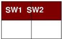
Where:
SW1 SW2 = 90 00h if no error
9.3.3.4. VERIFY_PASSWORD
Command Format (abData field in the PC_to_RDR_XfrBlock)
| Pseudo-APDU | |||||||
| CLA | INS | P1 | P2 | Lc | Pw(0) | Pw(1) | Pw(2) |
| FFh | 20h 00h | 03h | |||||
Where:
Pw(0), Pw(1), Pw(2) Passwords to be sent to memory card
P2 = 0000 00rp
where the two bits "rp" indicate the password to compare
r = 0: Write password,
r = 1: Read password,
p: Password set number,
rp = 01 for the secure code.
Response Data Format (abData field in the RDR_to_PC_DataBlock)
| SW1 | SW2ErrorCnt |
| 90h |
Where:
SW1 = 90h
SW2 (ErrorCnt)
= Error Counter. FFh indicates the verification is correct. 00h indicates the password is locked (or exceeded the maximum number of retries). Other values indicate the current verification has failed.
9.3.3.5. INITIALIZE_AUTHENTICATION
Command Format (abData field in the PC_to_RDR_XfrBlock)
| Pseudo-APDU | ||||||||
| CLA | INS | P1 | P2 | Lc | Q(0) | Q(1) | ... | Q(7) |
| FFh | 84h 00h | 00h | 08h | |||||
Where:
Q(0), Q(1)...Q(7) Host random number, 8 bytes
Response Data Format (abData field in the RDR_to_PC_DataBlock)
| SW1 SW2 | |
Where:
SW1 SW2 = 90 00h if no error
9.3.3.6. VERIFY_AUTHENTICATION
Command Format (abData field in the PC_to_RDR_XfrBlock)
| Pseudo-APDU | ||||||||
| CLA | INS | P1 | P2 | Lc | Ch(0) | Ch(1) | ... | Ch(7) |
| FFh | 82h 00h | 00h 08h | ||||||
Where:
Ch(0), Ch(1)...Ch(7)
Host challenge, 8 bytes
Response Data Format (abData field in the RDR_to_PC_DataBlock)
| SW1 | SW2 |
Where:
SW1 SW2 = 90 00h if no error
9.3.4. Memory Card – ATMEL AT88C1608
9.3.4.1. SELECT_CARD_TYPE
This command powers up and down the selected card that is inserted in the card reader and performs a card reset. It will also select the page size to be 16-byte page write.
Note: This command can only be used after the logical smart card reader communication has been established using the SCardConnect() API. For details of SCardConnect() API, please refer to PC/SC specifications.
Command Format (abData field in the PC_to_RDR_XfrBlock)
| Pseudo-APDU | ||||||
| CLA | INS | P1 | P2 | Lc | Card Type | |
| FFh | A4h | 00h | 00h | 01h | 04h | |
Response Data Format (abData field in the RDR_to_PC_DataBlock)
| SW1 | SW2 |
Where:
SW1 SW2 = 90 00h if no error
9.3.4.2. READ_MEMORY_CARD
Command Format (abData field in the PC_to_RDR_XfrBlock)
| Pseudo-APDU | ||||
| CLA | INS | Zone Address | Byte Address | MEM_L |
| FFh | ||||
Where:
INS = B0h for reading user zone = B1h for reading configuration zone or reading fuse
Zone Address = 0000 0A 10 A 9 A 8 b where A 10 is the MSB of zone address = don't care for reading fuse
Byte Address = A 7A6A5A4 A3A2A1A0b is the memory address location of the memory card
= 1000 0000b for reading fuse
MEM_L = Length of data to be read from the memory card
Response Data Format (abData field in the RDR_to_PC_DataBlock)
| BYTE 1 | ... | ... | BYTE N | SW1 | SW2 |
Where:
BYTE x Data read from memory card
SW1 SW2 = 90 00h if no error
9.3.4.3. WRITE_MEMORY_CARD
Command Format (abData field in the PC_to_RDR_XfrBlock)
| Pseudo-APDU | ||||||||
| CLA | INS | Zone Address | Byte Address | MEM_L | Byte 1 | ... | ... | Byte n |
| FFh | ||||||||
Where:
INS = D0h for writing user zone
= D1h for writing configuration zone or writing fuse
Zone Address = 0000 0A 10A9A8b where A10 is the MSB of zone address
= Don't care for writing fuse
Byte Address = A7 A6 A5 A4 A3 A2 A1 A0 b is the memory address location of the memory card
= 1000 0000b for writing fuse
MEM_L Length of data to be written to the memory card
Byte x Data to be written to the memory card
Response Data Format (abData field in the RDR_to_PC_DataBlock)
| SW1 SW2 | |
Where:
SW1 SW2 = 90 00h if no error
9.3.4.4. VERIFY_PASSWORD
Command Format (abData field in the PC_to_RDR_XfrBlock)
| Pseudo-APDU | ||||||||
| CLA | INS P1 | P2 Lc | Data | |||||
| FFh | 20h | 00h | 00h | 04h | RP | Pw(0) | Pw(1) | Pw(2) |
Where:
Pw(0), Pw(1), Pw(2) Passwords to be sent to memory card
RP = 0000 rp2 p1 p0 b
where the four bits "rp2p1p0" indicate the password to compare:
r = 0: Write password,
r = 1: Read password,
p2p1p0 : Password set number.
(rp2p1p0 = 0111 for the secure code)
Response Data Format (abData field in the RDR_to_PC_DataBlock)
| SW1 | SW2ErrorCnt |
| 90h |
Where:
SW1 = 90h
SW2 (ErrorCnt) = Error Counter. FFh indicates the verification is correct. 00h indicates the password is locked (or exceeded the maximum number of retries). Other values indicate the current verification has failed.
9.3.4.5. INITIALIZE_AUTHENTICATION
Command Format (abData field in the PC_to_RDR_XfrBlock)
| Pseudo-APDU | ||||||||
| CLA | INS | P1 | P2 | Lc | Q(0) | Q(1) | ... | Q(7) |
| FFh | 84h 00h | 00h | 08h | |||||
Where:
Byte Address
Memory address location of the memory card
Q(0), Q(1)...Q(7)
Host random number, 8 bytes
Response Data Format (abData field in the RDR_to_PC_DataBlock)
| SW1 | SW2 |
Where:
SW1 SW2 = 90 00h if no error
9.3.4.6. VERIFY_AUTHENTICATION
Command Format (abData field in the PC_to_RDR_XfrBlock)
| Pseudo-APDU | ||||||||
| CLA | INS | P1 | P2 | Lc | Q1(0) | Q1(1) | ... | Q1(7) |
| FFh | 82h 00h | 00h 08h | ||||||
Where:
Byte Address
Memory address location of the memory card
Q1(0), Q1(1)...Q1(7)
Host challenge, 8 bytes
Response Data Format (abData field in the RDR_to_PC_DataBlock)
| SW1 SW2 | |
Where:
SW1 SW2 = 90 00h if no error
9.3.5. Memory Card – SLE 4418/SLE 4428/SLE 5518/SLE 5528
9.3.5.1. SELECT_CARD_TYPE
This command powers up and down the selected card that is inserted in the card reader and performs a card reset.
Note: This command can only be used after the logical smart card reader communication has been established using the SCardConnect() API. For details of SCardConnect() API, please refer to PC/SC specifications.
Command Format (abData field in the PC_to_RDR_XfrBlock)
| Pseudo-APDU | |||||
| CLA | INS | P1 | P2 | Lc | Card Type |
| FFh | A4h 00h | 00h | 01h 05h | ||
Response Data Format (abData field in the RDR_to_PC_DataBlock)
| SW1 | SW2 |
Where:
SW1 SW2 = 90 00h if no error
9.3.5.2. READ_MEMORY_CARD
Command Format (abData field in the PC_to_RDR_XfrBlock)
| Pseudo-APDU | ||||
| CLA | INS | Byte Address | MEM_L | |
| MSB | LSB | |||
| FFh | B0h | |||
Where:
MSB Byte Address = 0000 00A 9A8b is the memory address location of the memory card
LSB Byte Address = A7 A6 A5 A4 A3 A2 A1 A0 b is the memory address location of the memory card
MEM_L Length of data to be read from the memory card
Response Data Format (abData field in the RDR_to_PC_DataBlock)
| BYTE 1 ... ... | BYTE N SW1 SW2 | ||||
Where:
BYTE x Data read from memory card
SW1, SW2 = 90 00h if no error
9.3.5.3. READ_PRESENTATION_ERROR_COUNTER_MEMORY_CARD (SLE 4428 and SLE 5528)
This command is used to read the presentation error counter for the secret code.
Command Format (abData field in the PC_to_RDR_XfrBlock)
| Pseudo-APDU | |||||
| CLA | INS | P1 | P2 | MEM_L | |
| FFh | B | 1h | 00h | 00h | 03h |
Response Data Format (abData field in the RDR_to_PC_DataBlock)
ERRCNT Error Counter. FFh indicates that the last verification is correct. 00h indicates that the password is locked (exceeded the maximum number of retries). Other values indicate that the last verification has failed.
DUMMY Two bytes dummy data read from the card
SW1 SW2 = 90 00h if no error
9.3.5.4. READ_PROTECTION_BIT
Command Format (abData field in the PC_to_RDR_XfrBlock)
| Pseudo-APDU | ||||
| CLA | INS | Byte Address | MEM_L | |
| MSB | LSB | |||
| FFh | B2h | |||
Where:
MSB Byte Address = 0000 00A 9A8b is the memory address location of the memory card
LSB Byte Address = A7 A6 A5 A4 A3 A2 A1 A0 b is the memory address location of the memory card
MEM_L Length of protection bits to be read from the card, in multiples of 8 bits. Maximum value is 32.
MEM_L = 1 + INT ((number of bits - 1) / 8)
Example: To read 8 protection bits starting from memory 0010h, the following pseudo-APDU should be issued:
FFh B2h 00h 10h 01h
Response Data Format (abData field in the RDR_to_PC_DataBlock)
| PROT 1 | ... | ... | PROT L | SW1 | SW2 |
Where:
PROT y Bytes containing the protection bits
SW1, SW2 = 9000h if no error
The arrangement of the protection bits in the PROT bytes is as follows:
| PROT 1 | PROT 2 | ... | |||||||||||||||||||||
| P8 | P7 | P6 | P5 | P4 | P3 | P2 | P1 | P16 | P15 | P14 | P13 | P12 | P11 | P10 | P9 | .. | .. | .. | .. | .. | .. | P18 | P17 |
Where:
Px is the protection bit of BYTE x in the response data
'0' byte is write protected
'1' byte can be written
9.3.5.5. WRITE_MEMORY_CARD
Command Format (abData field in the PC_to_RDR_XfrBlock)
| Pseudo-APDU | ||||||||
| CLA INS | Byte Address | MEM_L | Byte 1 | .... | .... | Byte N | ||
| MSB | LSB | |||||||
| FFh D0h | ||||||||
Where:
MSB Byte Address = 0000 00A 9A8b is the memory address location of the memory card
LSB Byte Address = A7A6A5A4 A3A2A1A0b is the memory address location of the memory card
MEM_L Length of data to be written to the memory card
Byte x Data to be written to the memory card
Response Data Format (abData field in the RDR_to_PC_DataBlock)
| SW1 | SW2 |
Where:
SW1 SW2 = 90 00h if no error
9.3.5.6. WRITE_PROTECTION_MEMORY_CARD
Each byte specified in the command is used in the card to compare the byte stored in a specified address location. If the data match, the corresponding protection bit is irreversibly programmed to '0'.
Command Format (abData field in the PC_to_RDR_XfrBlock)
| Pseudo-APDU | ||||||||
| CLA INS | Byte Address | MEM_L | Byte 1 | .... | .... | Byte N | ||
| MSB LSB | ||||||||
| FFh | D1h | |||||||
Where:
MSB Byte Address = 0000 00A 9 A 8 b is the memory address location of the memory card
LSB Byte Address = A 7A6A5A4 A3A2A1A0b is the memory address location of the memory card
MEM_L Length of data to be written to the memory card
Byte x Byte values to be compared with the data in the card starting at Byte Address. BYTE 1 is compared with the data at Byte Address; BYTE N is compared with the data at (Byte Address+N-1).
Response Data Format (abData field in the RDR_to_PC_DataBlock)
| SW1 SW2 | |
Where:
SW1 SW2 = 90 00h if no error
9.3.5.7. PRESENT_CODE_MEMORY_CARD (SLE 4428 and SLE 5528)
This command is used to submit the secret code to the memory card to enable the write operation with the SLE 4428 and SLE 5528 card, the following actions are executed:
- Search a '1' bit in the presentation error counter and write the bit to '0'.
- Present the specified code to the card.
- Try to erase the presentation error counter.
Command Format (abData field in the PC_to_RDR_XfrBlock)
| Pseudo-APDU | ||||||
| CLA | INS | P1 | P2 | MEM_L | CODE | |
| Byte 1 | Byte 2 | |||||
| FFh | 20h | 00h | 00h | 02h | ||
Where:
CODE Two bytes secret code (PIN)
Response Data Format (abData field in the RDR_to_PC_DataBlock)
| SW1 | SW2ErrorCnt |
| 90h |
Where:
SW1 = 90h
SW2 (ErrorCnt) = Error Counter. FFh indicates successful verification. 00h indicates that the password is locked (or exceeded the maximum number of retries). Other values indicate that current verification has failed.
9.3.6. Memory Card – SLE 4432/SLE 4442/SLE 5532/SLE 5542
9.3.6.1. SELECT_CARD_TYPE
This command powers down and up the selected card that is inserted in the card reader and performs a card reset.
Note: This command can only be used after the logical smart card reader communication has been established using the SCardConnect() API. For details of SCardConnect() API, please refer to PC/SC specifications.
Command Format (abData field in the PC_to_RDR_XfrBlock)
| Pseudo-APDU | ||||||
| CLA | INS | P1 | P2 | Lc | Card Type | |
| FFh | A4h | 00h | 00h | 01h | 06h | |
Response Data Format (abData field in the RDR_to_PC_DataBlock)
| SW1 SW2 | |
Where:
SW1 SW2 = 90 00h if no error
9.3.6.2. READ_MEMORY_CARD
Command Format (abData field in the PC_to_RDR_XfrBlock)
| Pseudo-APDU | ||||
| CLA | INS | P1 | Byte Address | MEM_L |
| FFh | B0h 00h | |||
Where:
Byte Address = A7 A6 A5 A4 A3 A2 A1 A0 b is the memory address location of the memory card
MEM_L Length of data to be read from the memory card
Response Data Format (abData field in the RDR_to_PC_DataBlock)
| BYTE 1 ... ... BYTE N SW1 SW2 | |||||
Where:
BYTE x Data read from memory card
SW1, SW2 = 90 00h if no error
9.3.6.3. READ_PRESENTATION_ERROR_COUNTER_MEMORY_CARD (SLE 4442 and SLE 5542)
This command is used to read the presentation error counter for the secret code.
Command Format (abData field in the PC_to_RDR_XfrBlock)
| Pseudo-APDU | |||||
| CLA | INS | P1 | P2 | MEM_L | |
| FFh | B | 1h | 00h | 00h | 04h |
Response Data Format (abData field in the RDR_to_PC_DataBlock)
ERRCNT Error counter. 07h indicates that the last verification is correct. 00h indicates that the password is locked (exceeded the maximum number of retries). Other values indicate that the last verification has failed.
DUMMY Three bytes dummy data read from the card
SW1 SW2 = 90 00h if no error
9.3.6.4. READ_PROTECTION_BITS
This command is used to read the protection bits for the first 32 bytes.
Command Format (abData field in the PC_to_RDR_XfrBlock)
| Pseudo-APDU | |||||
| CLA | INS | P1 | P2 | MEM_L | |
| FFh | B2h | 00h | 00h | 04h | |
Response Data Format (abData field in the RDR_to_PC_DataBlock)
| PROT 1 | PROT 2 | PROT 3 | PROT 4 | SW1 | SW2 |
Where:
PROT y Bytes containing the protection bits from protection memory
SW1, SW2 = 90 00h if no error
The arrangement of the protection bits in the PROT bytes is as follows:
| PROT 1 PROT 2 ... | |||||||||||||||||||||||
| P8 | P7 | P6 | P5 | P4 | P3 | P2 | P1 | P16 | P15 | P14 | P13 | P12 | P11 | P10 | P9 | .. | .. | .. | .. | .. | .. | P18 | P17 |
Where:
Px is the protection bit of BYTE x in the response data
'0' byte is write protected
'1' byte can be written
9.3.6.5. WRITE_MEMORY_CARD
Command Format (abData field in the PC_to_RDR_XfrBlock)
| Pseudo-APDU | ||||||||
| CLA | INS | P1 | Byte Address | MEM_L | Byte 1 | .... | .... | Byte N |
| FFh | D0h | 00h | ||||||
Where:
Byte Address = A7 A6 A5 A4 A3 A2 A1 A0 b is the memory address location of the memory card
MEM_L Length of data to be written to the memory card
Byte x Data to be written to the memory card
Response Data Format (abData field in the RDR_to_PC_DataBlock)
| SW1 | SW2 |
Where:
SW1 SW2 = 90 00h if no error
9.3.6.6. WRITE_PROTECTION_MEMORY_CARD
Each byte specified in the command is internally compared in the card with the byte stored at the specified address, and if the data match, the corresponding protection bit is irreversibly programmed to '0'.
Command Format (abData field in the PC_to_RDR_XfrBlock)
| Pseudo-APDU | ||||||||
| CLA | INS | P1 | Byte Address | MEM_L | Byte 1 | .... | .... | Byte N |
| FFh | D1h | 00h | ||||||
Where:
Byte Address = 000A 4 A3A2A1A0b (00h to 1Fh) is the protection memory address location of the memory card
MEM_L Length of data to be written to the memory card
Byte x Byte values to be compared with the data in the card starting at Byte Address. BYTE 1 is compared with the data at Byte Address; BYTE N is compared with the data at (Byte Address+N-1).
Response Data Format (abData field in the RDR_to_PC_DataBlock)
| SW1 | SW2 |
Where:
SW1 SW2 = 90 00h if no error
9.3.6.7. PRESENT_CODE_MEMORY_CARD (SLE 4442 and SLE 5542)
To submit the secret code to the memory card to enable the write operation with the SLE 4442 and SLE 5542 card, the following actions are executed:
- Search a '1' bit in the presentation error counter and write the bit to '0'.
- Present the specified code to the card.
- Try to erase the presentation error counter.
Command Format (abData field in the PC_to_RDR_XfrBlock)
| Pseudo-APDU | |||||||
| CLA | INS | P1 | P2 | MEM_L | CODE | ||
| Byte 1 | Byte 2 Byte 3 | ||||||
| FFh | 20h | 00h | 00h | 03h | |||
Where:
CODE Three bytes secret code (PIN)
Response Data Format (abData field in the RDR_to_PC_DataBlock)
| SW1 | SW2ErrorCnt |
| 90h |
Where:
SW1 = 90h
SW2 (ErrorCnt) = Error Counter. 07h indicates that the verification is correct. 00h indicates the password is locked (exceeded the maximum number of retries). Other values indicate that the current verification has failed.
9.3.6.8. CHANGE_CODE_MEMORY_CARD (SLE 4442 and SLE 5542)
This command is used to write the specified data as new secret code in the card.
The current secret code must have been presented to the card with the PRESENT_CODE command prior to the execution of this command.
Command Format (abData field in the PC_to_RDR_XfrBlock)
| Pseudo-APDU | |||||||
| CLA | INS P1 | P2 MEM_L | CODE | ||||
| Byte 1 | Byte 2 | Byte 3 | |||||
| FFh | D2h 00 | h 01h | 03h | ||||
Response Data Format (abData field in the RDR_to_PC_DataBlock)
| SW1 | SW2 |
Where:
SW1 SW2 = 90 00h if no error
9.3.7. Memory Card - SLE 4406/SLE 4436/SLE 5536/SLE 6636
9.3.7.1. SELECT_CARD_TYPE
This command powers down and up the selected card that is inserted in the card reader and performs a card reset.
Note: This command can only be used after the logical smart card reader communication has been established using the SCardConnect() API. For details of SCardConnect() API, please refer to PC/SC specifications.
Command Format (abData field in the PC_to_RDR_XfrBlock)
| Pseudo-APDU | ||||||
| CLA | INS | P1 | P2 | Lc | Card Type | |
| FFh | A4h | 00h | 00h | 01h | 07h | |
Response Data Format (abData field in the RDR_to_PC_DataBlock)
| SW1 SW2 | |
Where:
SW1 SW2 = 90 00h if no error
9.3.7.2. READ_MEMORY_CARD
Command Format (abData field in the PC_to_RDR_XfrBlock)
| Pseudo-APDU | ||||
| CLA | INS | P1 | Byte Address | MEM_L |
| FFh | B0h 00h | |||
Where:
Byte Address = Memory address location of the memory card
MEM_L Length of data to be read from the memory card
Response Data Format (abData field in the RDR_to_PC_DataBlock)
| BYTE 1 ... ... BYTE N SW1 SW2 | |||||
Where:
BYTE x Data read from memory card
SW1, SW2 = 90 00h if no error
9.3.7.3. WRITE_ONE_BYTE_MEMORY_CARD
This command is used to write one byte to the specified address of the inserted card. The byte is written to the card with LSB first, (i.e. the bit at card address 0 is regarded as the LSB of byte 0).
Four different WRITE modes are available for this card type, which are distinguished by a flag in the command data field:
a. Write
The byte value specified in the command is written to the specified address. This command can be used for writing personalization data and counter values to the card.
b. Write with carry
The byte value specified in the command is written to the specified address and the command is sent to the card to erase the next lower counter stage. Thus, this write mode can only be used for updating the counter value in the card.
c. Write with backup enabled (SLE 4436, SLE 5536 and SLE 6636 only)
The byte value specified in the command is written to the specified address. This command can be used for writing personalization data and counter values to the card. Backup bit is enabled to prevent data loss when card tearing occurs.
d. Write with carry and backup enabled (SLE 4436, SLE 5536 and SLE 6636 only)
The byte value specified in the command is written to the specified address and the command is sent to the card to erase the next lower counter stage. Thus, this write mode can only be used for updating the counter value in the card. Backup bit is enabled to prevent data loss when card tearing occurs.
With all write modes, the byte at the specified card address is not erased prior to the write operation and, hence, memory bits can only be programmed from '1' to '0'.
The backup mode available in the SLE 4436 and SLE 5536 card can be enabled or disabled in the write operation.
Command Format (abData field in the PC_to_RDR_XfrBlock)
| Pseudo-APDU | ||||||
| CLA | INS | P1 | Byte Address | MEM_L | MODE | BYTE |
| FFh | D0h 00h | 02h | ||||
Where:
Byte Address = Memory address location of the memory card
MODE Specifies the write mode and backup option
00h: Write
01h: Write with carry
02h: Write with backup enabled (SLE 4436, SLE 5536 and SLE 6636 only)
03h: Write with carry and with backup enabled (SLE 4436, SLE 5536 and SLE 6636 only)
BYTE Byte value to be written to the card
Response Data Format (abData field in the RDR_to_PC_DataBlock)
| SW1 SW2 | |
Where:
SW1 SW2 = 90 00h if no error
9.3.7.4. PRESENT_CODE_MEMORY_CARD
To submit the secret code to the memory card to enable the card personalization mode, the following actions are executed:
- Search a '1' bit in the presentation counter and write the bit to '0'.
- Present the specified code to the card.
The ACR38x (CCID) does not try to erase the presentation counter after the code submission. This must be done by the application software through a separate 'Write with carry' command.
Command Format (abData field in the PC_to_RDR_XfrBlock)
| Pseudo-APDU | ||||||||
| CLA | INS | P1 | P2 | MEM_L | CODE | |||
| ADDR | Byte 1 | Byte 2 | ||||||
| FFh | 20h | 00h | 00h | 04h | 09h | |||
Where:
ADDR Byte address of the presentation counter in the card
CODE Three bytes secret code (PIN)
Response Data Format (abData field in the RDR_to_PC_DataBlock)
| SW1 | SW2 |
Where:
SW1 SW2 = 90 00h if no error
9.3.7.5. AUTHENTICATE_MEMORY_CARD (SLE 4436, SLE 5536 and SLE 6636)
To read a card authentication certificate from a SLE 5536 or SLE 6636 card, the ACR38x (CCID) executes the following actions:
- Select Key 1 or Key 2 in the card as specified in the command.
- Present the challenge data specified in the command to the card.
- Generate the specified number of CLK pulses for each bit of authentication data computed by the card.
- Read 16 bits of authentication data from the card.
- Reset the card to normal operation mode.
The authentication has to be performed in two steps:
- Send the Authentication Certificate to the card.
- Get back two bytes of authentication data calculated by the card.
Step 1: Send Authentication Certificate to the Card.
Command Format (abData field in the PC_to_RDR_XfrBlock)
| Pseudo-APDU | |||||||||||
| CLA INS P1 | P2 MEM_L | CODE | |||||||||
| KEY | CLK_CNT | Byte 1 | Byte 2 | ...... | Byte 5 | Byte 6 | |||||
| FFh | 84h 00h | 00h | 08h | ||||||||
Where:
KEY Key to be used for the computation of the authentication certificate:
00h: Key 1 with no cipher block chaining
01h: Key 2 with no cipher block chaining
80h: Key 1 with cipher block chaining (SLE 5536 and SLE 6636 only)
81h: Key 2 with cipher block chaining (SLE 5536 and SLE 6636 only)
CLK_CNT Number of CLK pulses to be supplied to the card for the computation of each bit of the authentication certificate. Typical value is 160 clocks (A0h)
BYTE 1...6 Card challenge data
Response Data Format (abData field in the RDR_to_PC_DataBlock)
| SW1 | SW2 |
| 61h | 02h |
Where:
SW1 SW2 = 61 02h if no error, meaning two bytes of authentication data are ready. The authentication data can be retrieved by Get_Response command.
Step 2: Get back the Authentication Data (Get_Response).
Command Format (abData field in the PC_to_RDR_XfrBlock)
| Pseudo-APDU | |||||
| CLA | INS | P1 | P2 | MEM_L | |
| FFh | C0h | 00h | 00h | 02h | |
Response Data Format (abData field in the RDR_to_PC_DataBlock)
| CERT SW1 SW2 | |||
Where:
CERT: 16 bits of authentication data computed by the card. The LSB of BYTE 1 is the first authentication bit read from the card.
SW1 SW2 = 90 00h if no error
9.3.8. Memory Card – SLE 4404
9.3.8.1. SELECT_CARD_TYPE
This command powers up and down the selected card that is inserted in the card reader and performs a card reset.
Note: This command can only be used after the logical smart card reader communication has been established using the SCardConnect() API. For details of SCardConnect() API, please refer to PC/SC specifications.
Command Format (abData field in the PC_to_RDR_XfrBlock)
| Pseudo-APDU | |||||||
| CLA | INS | P1 | P2 | Lc | Card Type | ||
| FFh | A | 4h | 00h | 00h | 01 | 08h | |
Response Data Format (abData field in the RDR_to_PC_DataBlock)
| SW1 | SW2 |
Where:
SW1 SW2 = 90 00h if no error
9.3.8.2. READ_MEMORY_CARD
Command Format (abData field in the PC_to_RDR_XfrBlock)
| Pseudo-APDU | ||||
| CLA | INS | P1 | Byte Address | MEM_L |
| FFh | B0h 00h | |||
Where:
Byte Address = Memory address location of the memory card
MEM_L Length of data to be read from the memory card
Response Data Format (abData field in the RDR_to_PC_DataBlock)
| BYTE 1 ... ... | BYTE N SW1 SW2 | ||||
Where:
BYTE x Data read from memory card
SW1 SW2 = 90 00h if no error
9.3.8.3. WRITE_MEMORY_CARD
This command is used to write data to the specified address of the inserted card. The byte is written to the card with LSB first (i.e. the bit at card address 0 is regarded as the LSB of byte 0).
The byte at the specified card address is not erased prior to the write operation and, hence, memory bits can only be programmed from '1' to '0'.
Command Format (abData field in the PC_to_RDR_XfrBlock)
| Pseudo-APDU | ||||||||
| CLA | INS | P1 | Byte Address | MEM_L | Byte 1 | ... | ... | Byte N |
| FFh | D0h | 00h | ||||||
Where:
Byte Address = Memory address location of the memory card
MEM_L Length of data to be written to the memory card
BYTE Byte value to be written to the card
Response Data Format (abData field in the RDR_to_PC_DataBlock)
| SW1 SW2 | |
Where:
SW1 SW2 = 90 00h if no error
9.3.8.4. ERASE_SCRATCH_PAD_MEMORY_CARD
This command is used to erase the data of the scratch pad memory of the inserted card. All memory bits inside the scratch pad memory will be programmed to the state of '1'.
Note: To erase error counter or user area, please use the VERIFY_USER_CODE command as specified in the Section 9.3.8.5.
Command Format (abData field in the PC_to_RDR_XfrBlock)
| Pseudo-APDU | ||||
| CLA | INS | P1 | Byte Address | MEM_L |
| FFh D2h 00h | 00h | |||
Where:
Byte Address = Memory byte address location of the scratch pad Typical value is 02h
Response Data Format (abData field in the RDR_to_PC_DataBlock)
| SW1 SW2 | |
Where:
SW1 SW2 = 90 00h if no error
9.3.8.5. VERIFY_USER_CODE
This command is used to submit User Code (2 bytes) to the inserted card. User Code is to enable the memory access of the card.
The following actions are executed:
- Present the specified code to the card.
- Search a '1' bit in the presentation error counter and write the bit to '0'.
- Erase the presentation error counter. The User Error Counter can be erased when the submitted code is correct.
Command Format (abData field in the PC_to_RDR_XfrBlock)
| Pseudo-APDU | ||||||
| CLA | INS | Error Counter LEN | Byte Address | MEM_L | CODE | |
| Byte 1 | Byte 2 | |||||
| FFh | 20h 04h | 08h 02h | ||||
Where:
Error Counter LEN Length of presentation error counter in bits
Byte Address Byte address of the key in the card
CODE 2 bytes User Code
Response Data Format (abData field in the RDR_to_PC_DataBlock)
| SW1 SW2 | |
Where:
SW1 SW2 = 90 00h if no error = 63 00h if there are no more retries
Note: After SW1SW2 = 9000h has been received, read back the User Error Counter to check if the VERIFY_USER_CODE is correct. If the User Error Counter is erased and equals "FFh," the previous verification was successful.
9.3.8.6. VERIFY_MEMORY_CODE
This command is used to submit the Memory Code (4 bytes) to the inserted card. The Memory Code is used to authorize the reloading of the user memory, together with the User Code.
The following actions are executed:
- Present the specified code to the card.
- Search for a '1' bit in the presentation error counter and write the bit to '0'.
- Erase the presentation error counter. (Note: The Memory Error Counter cannot be erased.)
Command Format (abData field in the PC_to_RDR_XfrBlock)
Note: After SW1SW2 = 9000h has been received, read back the Application Area to check if the VERIFY_MEMORY_CODE is correct. If all data in the Application Area is erased and equals "FFh," the previous verification was successful.
9.3.9. Memory Card - AT88SC101/AT88SC102/AT88SC1003
9.3.9.1. SELECT_CARD_TYPE
This command powers down and up the selected card that is inserted in the card reader and performs a card reset.
Note: This command can only be used after the logical smart card reader communication has been established using the SCardConnect() API. For details of the SCardConnect() API, please refer to PC/SC specifications.
Command Format (abData field in the PC_to_RDR_XfrBlock)
| Pseudo-APDU | |||||
| CLA | INS | P1 | P2 | Lc | Card Type |
| FFh | A4h 00h | 00h | 01h 09h | ||
Response Data Format (abData field in the RDR_to_PC_DataBlock)
| SW1 SW2 | |
Where:
SW1 SW2 = 90 00h if no error
9.3.9.2. READ_MEMORY_CARD
Command Format (abData field in the PC_to_RDR_XfrBlock)
| Pseudo-APDU | ||||
| CLA | INS | P1 | Byte Address | MEM_L |
| FFh B0h 00h | ||||
Where:
Byte Address = Memory address location of the memory card
MEM_L Length of data to be read from the memory card
Response Data Format (abData field in the RDR_to_PC_DataBlock)
| BYTE 1 ... ... | BYTE N SW1 SW2 | ||||
Where:
BYTE x Data read from memory card
SW1 SW2 = 90 00h if no error
9.3.9.3. WRITE_MEMORY_CARD
This command is used to write data to the specified address of the inserted card. The byte is written to the card with LSB first (i.e. the bit at card address 0 is regarded as the LSB of byte 0).
The byte at the specified card address is not erased prior to the write operation and, hence, memory bits can only be programmed from '1' to '0'.
Command Format (abData field in the PC_to_RDR_XfrBlock)
| Pseudo-APDU | ||||||||
| CLA | INS | P1 | Byte Address | MEM_L | Byte 1 | .... | .... | Byte N |
| FFh | D0h | 00h | ||||||
Where:
Byte Address Memory address location of the memory card
MEM_L Length of data to be written to the memory card
BYTE Byte value to be written to the card
Response Data Format (abData field in the RDR_to_PC_DataBlock)
| SW1 | SW2 |
Where:
SW1 SW2 = 90 00h if no error
9.3.9.4. ERASE_NON_APPLICATION_ZONE
This command is used to erase the data in Non-Application Zones. The EEPROM memory is organized into 16-bit words. Although erases are performed on single bit, the ERASE operation clears an entire word in the memory. Therefore, performing an ERASE on any bit in the word will clear ALL 16 bits of that word to the state of '1'.
To erase Error Counter or the data in Application Zones, please refer to the following:
- ERASE APPLICATION ZONE WITH ERASE command as specified in Section 9.3.9.5.
- ERASE_APPLICATION_ZONE_WITH_WRITE_AND_ERASE command as specified in Section 9.3.9.6.
- VERIFY SECURITY CODE commands as specified in Section 9.3.9.7.
Command Format (abData field in the PC_to_RDR_XfrBlock)
| Pseudo-APDU | ||||
| CLA | INS | P1 | Byte Address | MEM_L |
| FFh | D2h 00h | 00h | ||
Where:
Byte Address: memory byte address location of the word to be erased
Response Data Format (abData field in the RDR_to_PC_DataBlock)
| SW1 SW2 | |
Where:
SW1 SW2 = 90 00h if no error
9.3.9.5. ERASE_APPLICATION_ZONE_WITH_ERASE
This command can be used in the following cases:
- AT88SC101: To erase the data in Application Zone with EC Function Disabled.
- AT88SC102: To erase the data in Application Zone 1.
- AT88SC102: To erase the data in Application Zone 2 with EC2 Function Disabled.
- AT88SC1003: To erase the data in Application Zone 1.
- AT88SC1003: To erase the data in Application Zone 2 with EC2 Function Disabled.
- AT88SC1003: To erase the data in Application Zone 3.
The following actions are executed for this command:
- Present the specified code to the card
- Erase the presentation error counter. The data in corresponding Application Zone can be erased when the submitted code is correct.
Command Format (abData field in the PC_to_RDR_XfrBlock)
| Pseudo-APDU | |||||||||
| CLA | INS | Error Counter LEN | Byte Address | MEM_L | CODE | ||||
| Byte 1 | Byte 2 ... | ... | Byte N | ||||||
| FFh | 20h 00h | ||||||||
Where:
Error Counter LEN
Length of presentation error counter in bits. The value should be 00h always.
Byte Address
Byte address of the Application Zone Key in the card. Please refer to the table below for the correct value.
| Byte Address | LEN | |
| AT88SC101: Erase Application Zone with EC function disabled | 96h | 04h |
| AT88SC102: Erase Application Zone 1 | 56h | 06h |
| AT88SC102: Erase Application Zone 2 with EC2 function disabled | 9Ch | 04h |
| AT88SC1003: Erase Application Zone 1 36h | 06h | |
| AT88SC1003: Erase Application Zone 2 with EC2 function disabled | 5Ch | 04h |
| AT88SC1003: Erase Application Zone 3 | C0h | 06h |
MEM_L
Length of the Erase Key. Please refer to the table above for the correct value.
CODE
N bytes of Erase Key
Response Data Format (abData field in the RDR_to_PC_DataBlock)
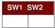
Where:
SW1 SW2 = 90 00h if no error
Note: After SW1SW2 = 9000h has been received, read back the data in Application Zone to check if the ERASE_APPLICATION_ZONE_WITH_ERASE is correct. If all data in Application Zone is erased and is equal to "FFh," the previous verification is successful.
9.3.9.6. ERASE_APPLICATION_ZONE_WITH_WRITE_AND_ERASE
This command can be used in the following cases:
- AT88SC101: To erase the data in Application Zone with EC Function Enabled.
- AT88SC102: To erase the data in Application Zone 2 with EC2 Function Enabled.
- AT88SC1003: To erase the data in Application Zone 2 with EC2 Function Enabled.
With EC or EC2 Function Enabled (that is, ECEN or EC2EN Fuse is undamaged and in "1" state), the following actions are executed:
- Present the specified code to the card.
- Search a '1' bit in the presentation error counter and write the bit to '0'.
- Erase the presentation error counter. The data in corresponding Application Zone can be erased when the submitted code is correct.
Command Format (abData field in the PC_to_RDR_XfrBlock)
Length of presentation error counter in bits. The value should be 80h always.
Byte Address
Byte address of the Application Zone Key in the card
| Byte Address | |
| AT88SC101 | 96h |
| AT88SC102 | 9Ch |
| AT88SC1003 | 5Ch |
CODE
4 bytes Erase Key
Response Data Format (abData field in the RDR_to_PC_DataBlock)
| SW1 | SW2 |
Where:
SW1 SW2
= 90 00h if no error
= 63 00h if there are no more retries
Note: After SW1SW2 = 9000h has been received, read back the data in Application Zone to check whether the ERASE_APPLICATION_ZONE_WITH_WRITE_AND_ERASE is correct. If all data in Application Zone is erased and is equal to "FFh," the previous verification is successful.
9.3.9.7. VERIFY_SECURITY_CODE
This command is used to submit Security Code (2 bytes) to the inserted card. Security Code is to enable the memory access of the card.
The following actions are executed:
- Present the specified code to the card
- Search a '1' bit in the presentation error counter and write the bit to '0'
- Erase the presentation error counter. The Security Code Attempts Counter can be erased when the submitted code is correct.
Command Format (abData field in the PC_to_RDR_XfrBlock)
| Pseudo-APDU | ||||||
| CLA INS | Error Counter LEN | Byte Address | MEM_L | CODE | ||
| Byte 1 | Byte 2 | |||||
| FFh | 20h 08h | 0Ah 02h | ||||
Where:
Error Counter LEN: Length of presentation error counter in bits
Byte Address: Byte address of the key in the card
CODE: 2 bytes Security Code
Response Data Format (abData field in the RDR_to_PC_DataBlock)
| SW1 | SW2 |
Where:
SW1, SW2 = 90 00h if no error = 63 00h if there are no more retries
Note: After SW1SW2 = 9000h has been received, read back the Security Code Attempts Counter (SCAC) to check whether the VERIFY_USER_CODE is correct. If SCAC is erased and is equal to "FFh," the previous verification is successful.
This command is used to blow the fuse of the inserted card. The fuse can be EC_EN Fuse, EC2EN Fuse, Issuer Fuse or Manufacturer's Fuse.
Note: The blowing of fuse is an irreversible process.
Command Format (abData field in the PC_to_RDR_XfrBlock)
| Pseudo-APDU | ||||||||
| CLA | INS | Error Counter LEN | Byte Address | MEM_L | CODE | |||
| Fuse Bit Addr (High) | Fuse Bit Addr (Low) | State of FUS Pin | State of RST Pin | |||||
| FFh | 05h 00h | 00h 04h | 01h | 00h or 01h | ||||
Where:
Fuse Bit Addr (2 bytes): Bit address of the fuse. Please refer to the table below for the correct value.
Bit address of the fuse. Please refer to the table below for the correct value.
State of FUS Pin
State of the FUS pin. Should always be 01h.
State of RST Pin
State of the RST pin. Please refer to the table below for the correct value.
| Fuse Bit Addr (High) | Fuse Bit Addr (Low) | State of RST Pin | ||
| AT88SC101 | Manufacturer Fuse | 05h | 80h | 01h |
| EC_EN Fuse | 05h | C9h | 01h | |
| Issuer Fuse | 05h | E0h | 01h | |
| AT88SC102 | Manufacturer Fuse | 05h | B0h | 01h |
| EC2EN Fuse | 05h | F9h | 01h | |
| Issuer Fuse | 06h | 10h | 01h | |
| AT88SC1003 | Manufacturer Fuse | 03h | F8h | 00h |
| EC2EN Fuse | 03h | FCh | 00h | |
| Issuer Fuse | 03h | E0h | 00h | |
Response Data Format (abData field in the RDR_to_PC_DataBlock)
| SW1 | SW2 |
Where:
SW1 SW2 = 90 00h if no error
9.4. Other Commands Access via PC_to_RDR_XfrBlock
9.4.1. GET_READER_INFORMATION
This command returns relevant information about the particular ACR38x (CCID) model and the current operating status, such as the firmware revision number, the maximum data length of a command and response, the supported card types, and whether a card is inserted and powered up or not.
Note: This command can only be used after the logical smart card reader communication has been established using the SCardConnect() API. For details of the SCardConnect() API, please refer to PC/SC specifications.
Command Format (abData field in the PC_to_RDR_XfrBlock)
| Pseudo-APDU | |||||
| CLA | INS | P1 | P2 | Lc | |
| FFh | 0 | 9h 00h | 00h | 10h | |
Response Data Format (abData field in the RDR_to_PC_DataBlock)
| FIRMWARE | MAX_C | MAX_R | C_TYPE | C_SEL | C_STAT | ||||||||||
Where:
FIRMWARE: 10 bytes of data for firmware version
MAX_C: The maximum number of command data bytes
MAX_R: The maximum number of data bytes that can be requested to be transmitted in a response
C_TYPE The card types supported by the ACR38x (CCID). This data field is a bitmap with each bit representing a particular card type. A bit set to '1' means the corresponding card type is supported by the reader and can be selected with the SELECT_CARD_TYPE command. The bit assignment is as follows:
| Byte | 1 | 2 | ||||||||||||||
| card type | F | E | D | C | B | A | 9 | 8 | 7 | 6 | 5 | 4 | 3 | 2 | 1 | |
Note: Refer to the next section for the correspondence between these bits and the respective card types.
C_SEL The currently selected card type. A value of 00h means that no card type has been selected.
C_STAT Indicates whether a card is physically inserted in the reader and whether the card is powered up:
00h: No card inserted
01h: Card inserted, not powered up
03h: Card powered up
Appendix A. Supported Card Types
The following table summarizes the card type returned by GET_READER_INFORMATION correspond with the respective card type.
| Byte | Card Type |
| 00h | Auto-select T=0 or T=1 communication protocol |
| 01h | I2C memory card (1, 2, 4, 8 and 16 kilobits) |
| 02h | I2C memory card (32, 64, 128, 256, 512 and 1024 kilobits) |
| 03h | Atmel AT88SC153 secure memory card |
| 04h | Atmel AT88SC1608 secure memory card |
| 05h | Infineon SLE 4418 and SLE 4428 |
| 06h | Infineon SLE 4432 and SLE 4442 |
| 07h | Infineon SLE 4406, SLE 4436 and SLE 5536 |
| 08h | Infineon SLE 4404 |
| 09h | Atmel AT88SC101, AT88SC102 and AT88SC1003 |
| 0Ch | MCU-based cards with T=0 communication protocol |
| 0Dh | MCU-based cards with T=1 communication protocol |
Table 3: Supported Card Types
Appendix B. Response Error Codes
The following table summarizes the possible error code returned by the ACR38x (CCID):
| Error Code Status |
| FFh SLOTERROR_CMD_ABORTED |
| FEh SLOTERROR_ICC_MUTE |
| FDh SLOTERROR_XFR_PARITY_ERROR |
| FCh SLOTERROR_XFR_OVERRUN |
| FBh SLOTERROR_HW_ERROR |
| F8h SLOTERROR_BAD_ATR_TS |
| F7h SLOTERROR_BAD_ATR_TCK |
| F6h SLOTERROR_ICC_PROTOCOL_NOT_SUPPORTED |
| F5h SLOTERROR_ICC_CLASS_NOT_SUPPORTED |
| F4h SLOTERROR_PROCEDURE_BYTE_CONFLICE |
| F3h SLOTERROR_DEACTIVATED_PROTOCOL |
| F2h SLOTERROR_BUSY_WITH_AUTO_SEQUENCE |
| E0h SLOTERROR_CMD_SLOT_BUSY |
Table 4: Response Error Codes
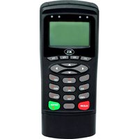


- LIST OF TABLES
- INTRODUCTION
- REFERENCE DOCUMENTS
- SYMBOLS AND ABBREVIATIONS
- FEATURES
- SMART CARD SUPPORT
- MCU CARDS
- MEMORY-BASED SMART CARDS
- SMART CARD INTERFACE
- SMART CARD POWER SUPPLY VCC (C1)
- PROGRAMMING VOLTAGE VPP (C6)
- CARD TYPE SELECTION
- INTERFACE FOR MICROCONTROLLER-BASED CARDS
- CARD TEARING PROTECTION
- POWER SUPPLY
- STATUS LED
- USB INTERFACE
- COMMUNICATION PARAMETERS
- ENDPOINTS
- COMMUNICATION PROTOCOL
- MEMORY CARD TYPE SELECTION
- COMMANDS
- CCID COMMAND PIPE BULK-OUT MESSAGES
- PC_TO_RDR_ICCPOWERON
- PC_TO_RDR_ICCPOWEROFF
- PC_TO_RDR_GETSLOTSTATUS
- PC_TO_RDR_XFRBLOCK
- PC_TO_RDR_GETPARAMETERS
- PC_TO_RDR_RESETPARAMETERS
- PC_TO_RDR_SETPARAMETERS
- CCID BULK-IN MESSAGES
- RDR_TO_PC_DATABLOCK
- RDR_TO_PC_SLOTSTATUS
- RDR_TO_PC_PARAMETERS
- MEMORY CARD COMMAND SET
- MEMORY CARD - 1, 2, 4, 8 AND 16 KILOBIT I2C CARD
- SELECT_CARD_TYPE
- SELECT_PAGE_SIZE
- READ_MEMORY_CARD
- WRITE_MEMORY_CARD
- MEMORY CARD - 32, 64, 128, 256, 512, AND 1024 KILOBIT I2C CARD
- MEMORY CARD – ATMEL AT88SC
- VERIFY_PASSWORD
- INITIALIZE_AUTHENTICATION
- VERIFY_AUTHENTICATION
- MEMORY CARD – ATMEL AT88C
- MEMORY CARD – SLE 4418/SLE 4428/SLE 5518/SLE
- READ_PRESENTATION_ERROR_COUNTER_MEMORY_CARD (SLE 4428 AND SLE 5528)
- READ_PROTECTION_BIT
- WRITE_PROTECTION_MEMORY_CARD
- PRESENT_CODE_MEMORY_CARD (SLE 4428 AND SLE 5528)
- MEMORY CARD – SLE 4432/SLE 4442/SLE 5532/SLE
- READ_PRESENTATION_ERROR_COUNTER_MEMORY_CARD (SLE 4442 AND SLE 5542)
- READ_PROTECTION_BITS
- PRESENT_CODE_MEMORY_CARD (SLE 4442 AND SLE 5542)
- CHANGE_CODE_MEMORY_CARD (SLE 4442 AND SLE 5542)
- MEMORY CARD - SLE 4406/SLE 4436/SLE 5536/SLE
- WRITE_ONE_BYTE_MEMORY_CARD
- PRESENT_CODE_MEMORY_CARD
- AUTHENTICATE_MEMORY_CARD (SLE 4436, SLE 5536 AND SLE 6636)
- MEMORY CARD – SLE
- ERASE_SCRATCH_PAD_MEMORY_CARD
- VERIFY_USER_CODE
- VERIFY_MEMORY_CODE
- MEMORY CARD - AT88SC101/AT88SC102/AT88SC
- ERASE_NON_APPLICATION_ZONE
- ERASE_APPLICATION_ZONE_WITH_ERASE
- ERASE_APPLICATION_ZONE_WITH_WRITE_AND_ERASE
- VERIFY_SECURITY_CODE
- OTHER COMMANDS ACCESS VIA PC_TO_RDR_XFRBLOCK
- GET_READER_INFORMATION
- APPENDIX A. SUPPORTED CARD TYPES
- APPENDIX B. RESPONSE ERROR CODES
Brand : ACS
Model : ACR38U-N1
Category : Payment terminal