
ENF656-EHW-INPR - Router ENCORE - Free user manual and instructions
Find the device manual for free ENF656-EHW-INPR ENCORE in PDF.


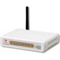
| Product Type | Wireless Router |
| Model | ENF656-EHW-INPR |
| Brand | ENCORE |
| Wireless Standard | IEEE 802.11ac (Wi-Fi 5) |
| Frequency Bands | 2.4 GHz and 5 GHz |
| Maximum Data Rate | Up to 1200 Mbps (300 Mbps on 2.4 GHz + 867 Mbps on 5 GHz) |
| Ethernet Ports | 4 x 10/100/1000 Mbps LAN, 1 x 10/100/1000 Mbps WAN |
| USB Port | 1 x USB 2.0 |
| Antennas | 4 x External Fixed Antennas |
| Security | WPA/WPA2, WPA3, SPI Firewall, MAC Filter, DoS Protection |
| Power Supply | 12V DC 1A |
| Dimensions (W x D x H) | 230 x 140 x 35 mm |
| Weight | 0.5 kg |
| Operating Temperature | 0°C to 40°C |
| Humidity | 10% to 90% non-condensing |
| LED Indicators | Power, WLAN, WAN, LAN (4), USB |
| Mounting Options | Desktop, Wall-mountable |
| Cleaning Instructions | Unplug device, wipe with a soft dry cloth. Do not use liquid cleaners. |
| Safety Warnings | Do not expose to water, heat, or direct sunlight. Place in a well-ventilated area. |
| Spare Parts Availability | Contact ENCORE support for replacement power adapters and antennas. |
Frequently Asked Questions - ENF656-EHW-INPR ENCORE
User questions about ENF656-EHW-INPR ENCORE
0 question about this device. Answer the ones you know or ask your own.
Ask a new question about this device
Download the instructions for your Router in PDF format for free! Find your manual ENF656-EHW-INPR - ENCORE and take your electronic device back in hand. On this page are published all the documents necessary for the use of your device. ENF656-EHW-INPR by ENCORE.
USER MANUAL ENF656-EHW-INPR ENCORE
Preliminary Datasheet
Product Features
■ Merges benefits from software and hardware modems
- Uses host's CPU without degrading performance
■ Distributes functions optimally between CPU and DSP
■ Cost savings
—CPU eliminates need for controller chip
—Reduced board size
—Superior price/performance ratio
■ Data modulation
—Data rates up to 56 kbps†
—ITU-V.92, V.90 compliant
—ITU-T V.34 (33,600 to 2,400 bps)
—ITU-T V.32 bis, V.23, V.22 bis, V.21
—Bell, 212A and 103
—Error correction: ITU V.42 and MNP, 2–4
—Data compression: ITU V.44, V.42 bis and MNP, 5
■ Fax modulation
—ITU-T V.17, V.26ter, V.29 to 14,400 bps —Fax Class 1 commands
PCI
—PCI 2.2-compliant
† Maximum speed allowed by the FCC is 53.333 kbps.
■ PC telephony
—International telephony support
—Voice compression: ADPCM, linear, and CL1
—4800, 7200, 8000, 9600, and 11025 samples/sec.
—Full-duplex, echo-cancelled digital speakerphone
—Telephone emulation for headset applications
—IS-101 Voice commands
—ITU-V.80 for videoconferencing
■ Power requirements
—DSP 3.3 V Pad, 1.3 V Core
—Automatic sleep and wake-up modes
—ACPI (advanced configuration power interface)
Packaging
—DSP: 128-pin LQFP
—AFE: 44-pin VQFP
■ Exceeds Microsoft*, PC 00 requirements
■ Microsoft, Windows*, TAPI-compliant
■ AT command-driven
Notice: This document contains preliminary information on new products in production. The specifications are subject to change without notice. Verify with your local Intel sales office that you have the latest datasheet before finalizing a design.
Information in this document is provided in connection with Intel ® products. No license, express or implied, by estoppel or otherwise, to any intellectual property rights is granted by this document. Except as provided in Intel's Terms and Conditions of Sale for such products, Intel assumes no liability whatsoever, and Intel disclaims any express or implied warranty, relating to sale and/or use of Intel products including liability or warranties relating to fitness for a particular purpose, merchantability, or infringement of any patent, copyright or other intellectual property right. Intel products are not intended for use in medical, life saving, or life sustaining applications.
Intel is a trademark or registered trademark of Intel Corporation or its subsidiaries in the United States and other countries.
Intel may make changes to specifications and product descriptions at any time, without notice.
Designers must not rely on the absence or characteristics of any features or instructions marked "reserved" or "undefined." Intel reserves these for future definition and shall have no responsibility whatsoever for conflicts or incompatibilities arising from future changes to them.
The 536EPXX may contain design defects or errors known as errata which may cause the product to deviate from published specifications. Current characterized errata are available on request.
Contact your local Intel sales office or your distributor to obtain the latest specifications and before placing your product order.
Copies of documents which have an ordering number and are referenced in this document, or other Intel literature may be obtained by calling 1-800-548-4725 or by visiting Intel's website at http://www.intel.com.
Copyright © Intel Corporation, 2001
*Third-party brands and names are the property of their respective owners.
1.0 Overview
The software upgradable 536EPXX chipset and reference design from Intel is targeted at modem and computer manufacturers. This new product is a leap forward in technology, performance and cost savings. The 536EPXX is a Host Accelerated Modem solution that combines and optimizes the best features from software and hardware modems. This unique hybrid delivers superior performance and is a price competitive modem.
The 536EPXX uses the host computer's CPU to replace the modem's controller without degrading CPU performance. Since today's CPUs are well equipped to handle Digital Signal Processing (DSP), some of the DSP functions are diverted to the CPU. However, to prevent a decrease in CPU and modem performance, a separate and less expensive DSP chip is used to share the load. Maximum system and modem performance is maintained by splitting the processing optimally between the CPU and the DSP.
Unlike software modems, there is no performance penalty because the CPU does not handle all of the controller and DSP functions. Instead, functions have been strategically optimized for accelerated performance by either the CPU or the DSP depending on which device can perform them most efficiently—delivering a price-performance ratio neither software- nor hardware-only modems can match.
Optimizing CPU usage in this manner eliminates the need for a controller and reduces the size of the DSP, thereby reducing part count, board size and the amount of silicon used. These cost saving advantages make the 536EPXX a superior high-performance and feature-rich alternative to software modems.
With an integrated PCI interface, this ITU-V.92 solution provides a complete set of standard data/ fax/voice and speakerphone features. Effective data receive rates of up to 56K (53.333 kbps FCC max.) ensures interoperability with major Internet service providers around the world. Chipset features also include ITU-V.80 videoconferencing. The 536EPXX exceeds Microsoft* PC 00 specifications for Windows* and is TAPI and PCI 2.1 compliant. It satisfies legacy applications and supports all requirements for PC-based communications, including all standard AT commands for data, Class 1 fax and IS-101 voice.
1.1 Versatile 56K Platform
With many advanced features already built in, the 536EPXX is a versatile platform for future development. By using the host computer's CPU, the 536EPXX can leverage the latest developments in CPU technology. These advances can be taken advantage of quickly because the controller code can be modified in a "C" code development environment. Thus, new features and products can be brought to market faster and less expensively than ever before. And end users can easily upgrade to the newest communication technology by downloading and installing software upgrades directly from the modem or computer manufacturer's internet site.
1.2 Integrated PCI & Mini-PCI Interface
The integrated design supports PCI and Mini-PCI interfaces, and allows the device to transfer data from the DSP to the host system's CPU faster than ISA or serial solutions. The integrated interface also eliminates the ISA bridge chip requirement which helps to reduce part count, board space and cost.
1.3 Satisfies Legacy Applications
The 536EPXX supports all PC-based communication requirements. Its robust host-based controller software and powerful DSP support all standard AT commands for data, Class 1 fax and IS-101 voice.
1.4 Comprehensive Telephony Features
Voice telephony is becoming increasingly important. The 536EPXX offers a complete telephony interface with Caller ID, voice mail, answering machine capabilities, tone generation and detection, call progress control, telephone emulation and full-duplex digital speakerphone. All voice features are fully compliant with Microsoft's Unimodem V and TAPI standards, and all voice commands comply with IS-101 voice command standards. Intel also provides DAA design recommendations that support international telephony applications.
1.5 Reference Design Available
Intel provides a reference design that demonstrates chipset applications for several common configurations. The design documentation includes a schematic (OrCAD), bill of materials, block diagram and a description of operation.
1.6 Minimal Component Design
The 536EPXX was designed to reduce part count, board area and the amount of silicon used. These design considerations significantly reduce the cost of the 536EPXX without sacrificing quality or performance. The 536EPXX solution is a sleek, compact and cost effective alternative to both software- and hardware-only modems.
1.7 Reduced EMI/RFI Emissions
A single low-frequency crystal serves as a clock for the DSP in the 536EPXX chipsets. The single-crystal design minimizes high-frequency harmonics and simplifies EMI/RFI design considerations.
Figure 3. Functional Block Diagrams

flowchart
graph TD
    subgraph 536EPU/G["536EPU/G"]
        A["HOST COMPUTER"] <-->|PCI BUS| B["DSP DQ82536"]
        C["NVRAM"] <--> B
        B <--> D["Silicon CODEC/DAA"]
        D --> E["TIP RING"]
    end

    subgraph_536EPA["536EPA"]
        F["HOST COMPUTER"] <-->|PCI BUS| G["DSP DQ82536"]
        H["NVRAM"] <--> G
        G <--> I["AFE MD1724"]
        I <--> J["DAA"]
        J --> K["TIP RING"]
        L["MICROPHONE / SPEAKER (OPTIONAL)"]
    end
Figure 3. Functional Block Diagrams (Continued)

flowchart
graph LR
    subgraph "536EPUS/GS/GL"
        A["HOST COMPUTER"] <-->|PCI BUS| B["DSP DQ82536"]
        C["NVRAM"] <--> B
        B <--> D["Silicon CODEC/DAA"]
        D --> E["TIP"]
        D --> F["RING"]
        G["AFE MD1724 (OPTIONAL)"] <--> H["MICROPHONE / SPEAKER (OPTIONAL)"]
        I["Host COMPUTER"] <-->|PCI BUS| J["DSP DQ82536"]
        K["NVRAM"] <--> J
        J <--> L["AFE MD1724"]
        M["AFE MD1724 (OPTIONAL)"] <--> N["DAA"]
        O["MICROPHONE / SPEAKER (OPTIONAL)"]
        P["TIP"]
        Q["RING"]
    end
6.0 Chipset Descriptions
The 536EPXX is a Host Accelerated Modem chipset family consisting of a DSP (digital signal processor), and a Silicon Laboratories CODEC/DAA or an Intel Analog Front End (AFE). These chipsets support a variety of applications and need no additional firmware development. The current 536EPXXchipsets are shown in Table 12 “Chipset Composition (PCI & Mini-PCI)” with their corresponding DSP and AFE device part numbers. Please contact Intel to verify current part numbers and technical information.
6.1 Host Controller Software
The host-based controller software contains code for all controller functions for Group 3 Fax mode, Data mode (including error correction and data compression), and Voice mode.
6.1.1 Digital Signal Processor (DSP)
The DQ82536 digital signal processor (DSP) performs all digital signal processing functions for the chipset, including modulation, echo cancellation, call progress monitoring, and voice processing.
The DSP requires a 3.3 V and 1.3 V power supply, which takes advantage of the latest manufacturing technologies. The PCI bus accommodates either 5-V or 3.3-V designs reducing power consumption.
6.2 Analog Front End Device (AFE)
The MD1724 AFE device uses Delta-Sigma techniques to convert analog information from a telephone line to digital information that can be processed by the DSP. In addition to its analog circuitry, the modem's Delta-Sigma function incorporates unique and proprietary digital-to-analog and analog-to-digital features. These features improve receiver accuracy, which in turn improves performance at low levels of receive signal.
Compared to other analog front-end technologies, the Delta-Sigma implementation better stabilizes the function of the AFE devices and makes them less sensitive to board layout than other analog front end technologies. Since a significant amount of signal processing is performed by digital rather than analog techniques, Delta-Sigma analog-to-digital conversion considerably improves signal quality.
For basic data, fax, and voice modes of operation, a single AFE device is needed. For full-duplex echo cancelled speakerphone applications, an additional AFE device is required. The AFEs require a 5-V power supply; however, the interface is 3.3-V-capable.
6.3 CODEC/DAA
The 536EPXX chipset uses a Silicon DAA to interface to the telephone line. The Silicon DAA replaces an analog front end (AFE), an isolation transformer, relays, opto-isolators and a hybrid.
7.0 Modes of Operation
The 536EPXX chipset family provides complete modem functions for the following modes: Group 3 Fax, Data, IS-101 Voice, V.42/MNP 2–4 (Microcom Networking Protocol Classes 2 through 4), Error correction, V.44, V.42 bis/MNP 5 (Microcom Networking Protocol Class 5), and Videoconferencing. Each mode has its own unique AT command set. The data rates and modulation schemes for Data and Fax modes are presented in Table 15 on page 25. Additionally, special modes of operation exist for power management and loopback testing.
7.1 Modes
7.1.1 Data Mode
In data mode, the 536EPXX chipsets send at an effective rate of 33.6 kbps and receive at 53.333 kbps using ITU-V.92. The 56K receive rates can be achieved only in connections with equipment-compatible ISPs (internet service providers). See Table 15 on page 25 for connection rates. Both chipset families implement all data rates and modulation schemes for ITU-T (International Telecommunications Union—Telecommunications) standards V.34, V.32 bis, V.32, V.22 bis, V.22, V.21, and Bell 212A, Bell 103. Both families implement a standard (TIES) Data mode AT command set, which is compatible with any communication application software that supports the Hayes* AT command set.
7.1.2 Fax Mode
In fax mode, the chipsets operate at up to 14.4 kbps (transmit and receive) and implement all the data rates and modulation schemes for ITU-T standards V.17, V.29, V.27 ter, and V.21 ch2. The chipsets implement a standard Fax mode AT command set compatible with any communication application software that supports EIA/TIA-578 Fax Class 1 standards.
7.1.3 Voice Mode
All chipsets support Telephone-Emulation mode, IS-101 voice commands, and record and playback message capabilities. Telephone-Emulation mode allows a handset/microphone-speaker and modem to be used as a complete telephone. In Telephone-Emulation mode, the received data from the AFE (MD1724) microphone interface is looped back to the AFE analog transmit pins. In voice mode, the message record and playback abilities are accessed by the extended IS-101 AT commands.
7.1.4 Error Correction and Data Compression Modes
The Intel platform supports error correction (V.42/MNP 2–4) and data compression (V.44 and V.42 bis/MNP 5). Error correction ensures error-free data transfer. Data compression substantially increases the modem data throughput over the basic data rate throughput. Depending on the data stream, MNP 5 can provide compression ratios of up to two-to-one. Alternately, ITU-T V.44 can provide up to 25% more compression than the V.42 bis.
7.1.5 Videoconferencing (V.80) Support
The 536EPXX supports the ITU-V.80 recommendation. This option ensures compatibility with host-based H.324 videoconferencing application software. The 536EPXX chipsets support both transparent and framed submodes of the V.80 synchronous access mode, plus Voice Call First and full-duplex speakerphone.
7.1.6 Loopback Test Modes
In all modes except V.92, modem-to-DTE and modem-to-modem communication integrity can be tested with loopback tests. The AT&T1 command initiates the local analog loopback test.
7.2 Other Features
7.2.1 Full-Duplex Speakerphone
The 536EPXX supports full-duplex speakerphone with internal adaptive echo cancellation. Phone users can talk simultaneously without the remote user hearing an echo.
7.2.2 Transmit Levels
The factory default transmit level for V.92 and V.34 transmission is -10 dBm ±1 dB at Tip and Ring. Data and fax use separate transmission levels. The transmit level can be programmed using the international configuration utility.
Important: Current download speeds are limited to 53.33 kbps due to FCC rules that restrict modem power output.
7.2.3 Transmit Tone Levels
The modem generates DTMF, answer, call, and guard tones. The specifications for each tone are provided in Table 13 and Table 14 on page 24. The transmit level can be programmed using the Intel configuration utility.
7.2.4 Receive Level
The receiver can accommodate a receive signal from -9 dBm to -43 dBm. The DCD (data carrier detect) function is activated at -43 dBm and above; it is deactivated at -48 dBm and below.
7.2.5 Receiver Tracking
The receiver compensates for up to ±7 Hz of carrier-frequency offset in V.34 mode.
7.2.6 Equalizers
Automatic adaptive and compromise equalizers are provided to compensate for line distortions.
7.2.7 Call Progress
The modem monitors the detection of call-progress tones during call origination and reports them to the DTE. Call-progress tones include dial, busy, ringback, and answer.
7.2.8 Caller ID
Caller ID is a service that allows the user to see the caller's telephone number and name. Caller ID also provides information on call date and time.
7.2.9 International Support
The Intel chipsets support international applications. For information on specific countries, contact your local Intel sales office at the address listed on the back cover of this document.
Table 13. Transmit Tones
| Tone Value | Application | |
| Calling tone | 1100 Hz Fax originator | |
| 1300 Hz Data originator | ||
| Answer tone | 2100 Hz Data/fax (ITU-T) | |
| 2225 Hz Data (Bell mode) | ||
| Guard tone | 1800 Hz | Data/fax (answer mode) |
| 550 Hz | ||
Table 14. DTMF Tone Pairs
| Dial Digit | Tone 1 (Hz) | Tone 2 (Hz) |
| 0 941 | 1336 | |
| 1 697 | 1209 | |
| 2 697 | 1336 | |
| 3 697 | 1447 | |
| 4 770 | 1209 | |
| 5 770 | 1336 | |
| 6 770 | 1477 | |
| 7 852 | 1209 | |
| 8 852 | 1336 | |
| 9 852 | 1447 | |
| * | 941 1209 | |
| # 941 | 1447 | |
| A | 697 1633 | |
| B 770 | 1633 | |
| C 852 | 1633 | |
| D 941 | 1633 |
Table 15. Communication Modes and Data Rates
| Application | Mode Data | Rate (bps) Modulation | Baud Rate (symbols/sec.) | Carrier Frequency (Hz) | Constellation Points | |
| Fax | V.17 | 14,400 TCM | 2400 1800 128 | |||
| 12,000 TCM | 2400 1800 64 | |||||
| 9600 | TCM 2400 | 1800 32 | ||||
| 7200 | TCM 2400 | 1800 16 | ||||
| V.29 | 9600 | QAM | 2400 1700 | 16 | ||
| 7200 | QAM | 2400 1700 | 8 | |||
| 4800 | QAM | 2400 1700 | 4 | |||
| V.27 ter | 4800 | DPSK | 1600 1800 | 8 | ||
| 2400 | DPSK | 1200 1800 | 4 | |||
| V.21 | 300 | FSK | 300 | 1650 M/1850 S | 2 | |
| Application | Mode | Data Rate (bps) | Modulation | Baud Rate (symbols/sec.) | Carrier Frequency (Hz) | Constellation Points |
| Data | V.92 Modea (V.92 receive path) | \( 57333^b, 56000, 54666, 53333, 52000, 50666, 49333, 48000, 46666, 45333, 44000, 42666, 41333, 40000, 38666, 37333, 36000, 34666, 33333, 32000, 30666, 29333, 28000 | PCM 8000 | N/A(Baseband) | Variablec | |
| V.92 Mode(V.34 transmit path) | 48000, 46666, 45333, 44000, 42666, 41333, 40000, 38666, 37333, 36000, 34666, 33333, 32000, 30666, 28000, 26666, 25333, 24000 | TCM | 342932003000 | Variable Variable | c | |
| V.34 | 33,600, 31,200, 28,800, 26,400, 24,000, 21,600, 19,200, 16,800, 14,400, 12,000, 9600, 7200, 4800, 2400 | TCM Variable | d | Variablee | Variablec | |
| V.32bis | 14,400 TCM | 2400 1800 128 | ||||
| 12,000 TCM | 2400 1800 64 | |||||
| 9600 TCM | 2400 1800 32 | |||||
| 7200 TCM | 2400 1800 16 | |||||
| 4800 TCM | 2400 1800 4 | |||||
| V.32 | 9600 TCM | 2400 1800 32 | ||||
| 9600 QAM | 2400 1800 16 | |||||
| 4800 QAM | 2400 1800 4 | |||||
| V.22 bis | 2400 | QAM | 600 | 1200/2400 | 16 | |
| V.22 | 1200 | DPSK 600 | 1200/2400 4 | |||
| Data (cont.) | V.21 | 300 | FSK | 300 | 980 M/1650 M1180 S/1850 S | 2 |
| Bell*212A | 1200 | DPSK 600 | 1200/2400 4 | |||
| Bell103 | 300 | FSK | 300 | 1270 M/2225 M1070 S/2025 S | 2 | |
a. V.92 data receive rates of up to 56 kbps can be achieved only in connections with equipment-compatible ISPs (internet service providers).
b. FCC regulations do not allow the 57,333, 56,000, and 54,666 kbps data rates to be supported.
c. Intel supports the normal and expanded constellations for each baud and data rate.
d. Intel supports five of the six baud rates specified by the ITU-T (International Telecommunications Union-Telecommunications): 2400, 2743, 3000, 3200, and 3429 symbols/second. The ITU-T's optional baud rate of 2800 symbols/second is not supported.
e. The high and low carrier frequencies specified by ITU-T are supported for each baud rate.
8.0 Hardware Interfaces
The 536EPXX chipset supports hardware interfaces for the host, expansion bus, non-volatile RAM (NVRAM), CODEC/DAA, speaker, microphone, and general-purpose I/O functions. The hardware interfaces are demonstrated below.
Figure 4. Modem System Block Diagram (536EPXX)

flowchart
graph LR
    A["HOST COMPUTER"] -->|PCI BUS| B["DSP DQ82536"]
    C["NVRAM"] <--> B
    B <--> D["CODEC"]
    D <--> E["DAA"]
    E --> F["TIP"]
    E --> G["RING"]
    B <--> H["AFE MD1724"]
    H <--> I["MICROPHONE / SPEAKER (OPTIONAL)"]
8.1 NVRAM Interface
536EPXX is designed to support either 2K or 4K EEPROM in x8 or x16 mode. NVRAM can be used to customize the Subsystem Vendor ID and Subsystem ID per the manufacturer's requirement. 536EPXX can also be used without the NVRAM, in this case 536EPXX will default to one of the ID's listed in Table 16 depending on how the GPIO 8 through 11 are tied.
PCI configuration data to use. Table 16 describes this.
Table 16. PCI Subsystem Vendor ID and Subsystem ID with No EEPROM
| GPIO[10:8] Subsystem | Vendor Subsystem ID | |
| 000 Reserved 1040h | ||
| 001 Reserved 1040h | ||
| 010 Reserved 1040h | ||
| 011 Reserved 1040h | ||
| 100 Reserved 1040h | ||
| 101 Reserved 1040h | ||
| 110 Reserved 1040h | ||
| 111 Reserved 1040h | ||
| 000 | Intel (ID = 8086) | 1000h |
| 001 Intel (ID = 8086) | 1001h | |
| 010 Intel (ID = 8086) | 1002h | |
| 011 Intel (ID = 8086) | 1003h | |
| 100 Intel (ID = 8086) | 1004h | |
| 101 Intel (ID = 8086) | 1005h | |
| 110 Intel (ID = 8086) | 1006h | |
| 111 Intel (ID = 8086) | 1007h |
8.2 DAA Interface
A DAA (Data Access Arrangement) is the interface between the modem chipset and the telephone network. The DAA interface controls the telephone line off-hook relays, detects ring signals, and transmits and receives analog signals.
8.3 ACPI Interface
The 536EPXX supports the ACPI (Advanced Configuration and Power Interface) power management specification: the operating system puts system components into low-power states when not active. These chipsets support three power states: D0, D2, and D3 cold .
8.3.1 D0
All PCI bus functions must support the D0 state and go to D0 before use. On power up, the function is in an uninitialized state. When initialized by system software, the function goes to D0 active.
8.3.2 D2
D2 may be entered when a PCI bus function is idle. This provides significant power savings and allows the function to return to the original condition. In this state only PCI configuration access is allowed. Memory and I/O access is not allowed. Configuration space must be accessible by system software while D2 is active.
System software must restore the function to D0 active before memory or I/O space can be accessed. Initiated activity such as bus mastering and functional interrupt request generation occur only after the function has been restored to active state.
Important: A minimum recovery time of 200 µ s from D2 to D0 is required before the next function can be accessed. Attempted access sooner than this could result in undefined system behavior.
8.3.3 D3 cold
Switching from main supply outputs to the auxiliary power source requires strict power budgeting of slots, determining those to consume full 3.3Vaux power. A PCI function must draw no more than 20 mA through the 3.3Vaux pin when in D3cold if the PME_En bit is cleared. If a PCI function has been enabled for PME# generation before entering D3cold , the PCI add-in card can continue to draw up to 375 mA through the 3.3Vaux pin while in D3cold .
8.3.4 Speaker Interface
The AFE device internally implements both the volume control and amplifier necessary to drive an external speaker. The output of the internal amplifier can be connected directly to a speaker or to the input of the host speaker amplifier. The internal amplifier is capable of driving a maximum load of 40 Ω. The speaker volume is controlled by the ATLn command.
8.3.5 Microphone Interface
The MD1724 AFE device provides a microphone interface that connects a microphone or handset to the modem with a minimum of external parts. This microphone input can then be used for local Voice record mode or for Telephone-Emulation mode.
8.3.6 General-Purpose I/O Interface
To customize the modem design, the DSP provides 14 general-purpose pins that can be used to control or monitor external circuitry.
Some of the general-purpose pins can be configured for specific functions (such as a Caller ID relay, CIDREL*). Pin functions can be controlled via the host controller code. Some Voice mode functions are enhanced by adding external circuitry for remote hang-up detection, extension phone pickup, or hang-up detection.
- Preliminary Datasheet
- Product Features
- Overview
- Versatile 56K Platform
- Integrated PCI & Mini-PCI Interface
- Satisfies Legacy Applications
- Comprehensive Telephony Features
- Reference Design Available
- Minimal Component Design
- Reduced EMI/RFI Emissions
- Chipset Descriptions
- Host Controller Software
- Digital Signal Processor (DSP)
- Analog Front End Device (AFE)
- CODEC/DAA
- Modes of Operation
- Modes
- Data Mode
- Fax Mode
- Voice Mode
- Error Correction and Data Compression Modes
- Videoconferencing (V.80) Support
- Loopback Test Modes
- Other Features
- Full-Duplex Speakerphone
- Transmit Levels
- Transmit Tone Levels
- Receive Level
- Receiver Tracking
- Equalizers
- Call Progress
- Caller ID
- International Support
- Hardware Interfaces
- NVRAM Interface
- DAA Interface
- ACPI Interface
- D0
- D2
- D3 cold
- Speaker Interface
- Microphone Interface
- General-Purpose I/O Interface
Brand : ENCORE
Model : ENF656-EHW-INPR
Category : Router