IDK-2112N-K2SVA2E - Suivi Advantech - Free user manual and instructions
Find the device manual for free IDK-2112N-K2SVA2E Advantech in PDF.

User questions about IDK-2112N-K2SVA2E Advantech
0 question about this device. Answer the ones you know or ask your own.
Ask a new question about this device
Download the instructions for your Suivi in PDF format for free! Find your manual IDK-2112N-K2SVA2E - Advantech and take your electronic device back in hand. On this page are published all the documents necessary for the use of your device. IDK-2112N-K2SVA2E by Advantech.
USER MANUAL IDK-2112N-K2SVA2E Advantech
natural_image
Illustration of four electronic circuit boards with white outlines on a purple background (no text or symbols)IDK-2112 Series
12.1" SVGA (LED Backlight)
Copyright
The documentation and the software included with this product are copyrighted 2015 by Advantech Co., Ltd. All rights are reserved. Advantech Co., Ltd. reserves the right to make improvements in the products described in this manual at any time without notice. No part of this manual may be reproduced, copied, translated or transmitted in any form or by any means without the prior written permission of Advantech Co., Ltd. Information provided in this manual is intended to be accurate and reliable. However, Advantech Co., Ltd. assumes no responsibility for its use, nor for any infringements of the rights of third parties, which may result from its use.
Acknowledgements
AMI is a trademark of American Megatrends Inc.
IBM and PC are trademarks of International Business Machines Corporation.
Intel® Core 2 Quad, Pentium Dual Core and Celeron are trademarks of Intel Corporation.
WinBond is a trademark of Winbond Corporation.
All other product names or trademarks are properties of their respective owners.
Part No. 2006211212 Edition 3
Printed in Taiwan October 2015
A Message to the Customer
Advantech Customer Services
Each and every Advantech product is built to the most exacting specifications to ensure reliable performance in the harsh and demanding conditions typical of industrial environments. Whether your new Advantech equipment is destined for the laboratory or the factory floor, you can be assured that your product will provide the reliability and ease of operation for which the name Advantech has come to be known.
Your satisfaction is our primary concern. Here is a guide to Advantech's customer services. To ensure you get the full benefit of our services, please follow the instructions below carefully.
Technical Support
We want you to get the maximum performance from your products. So if you run into technical difficulties, we are here to help. For the most frequently asked questions, you can easily find answers in your product documentation. These answers are normally a lot more detailed than the ones we can give over the phone.
So please consult this manual first. If you still cannot find the answer, gather all the information or questions that apply to your problem, and with the product close at hand, call your dealer. Our dealers are well trained and ready to give you the support you need to get the most from your Advantech products. In fact, most problems reported are minor and are able to be easily solved over the phone.
In addition, free technical support is available from Advantech engineers every business day. We are always ready to give advice on application requirements or specific information on the installation and operation of any of our products.
Product Warranty (2 years)
Advantech warrants to you, the original purchaser, that each of its products will be free from defects in materials and workmanship for two years from the date of purchase.
This warranty does not apply to any products which have been repaired or altered by persons other than repair personnel authorized by Advantech, or which have been subject to misuse, abuse, accident or improper installation. Advantech assumes no liability under the terms of this warranty as a consequence of such events.
Because of Advantech's high quality-control standards and rigorous testing, most of our customers never need to use our repair service. If an Advantech product is defective, it will be repaired or replaced at no charge during the warranty period. For out-of-warranty repairs, you will be billed according to the cost of replacement materials, service time and freight. Please consult your dealer for more details.
If you think you have a defective product, follow these steps:
- Collect all the information about the problem encountered. (For example, CPU speed, Advantech products used, other hardware and software used, etc.) Note anything abnormal and list any onscreen messages you get when the problem occurs.
- Call your dealer and describe the problem. Please have your manual, product, and any helpful information readily available.
- If your product is diagnosed as defective, obtain an RMA (return merchandise authorization) number from your dealer. This allows us to process your return more quickly.
- Carefully pack the defective product, a fully-completed Repair and Replacement Order Card and a photocopy proof of purchase date (such as your sales receipt) in a shippable container. A product returned without proof of the purchase date is not eligible for warranty service.
- Write the RMA number visibly on the outside of the package and ship it prepaid to your dealer.
Contents
Chapter 1 Overview......1
1.1 General Description 2
1.2 Specifications 2
1.2.1 LCD Panel.... 2
1.2.2 LED Driver Board.... 2
1.2.3 Touch Screen (R series) 2
1.2.4 Environment.... 2
1.3 Mechanical Characteristics ...... 3
1.4 Functional Block Diagram 5
Figure 1.1 Function block diagram .... 5
1.5 Absolute Maximum Ratings 5
1.5.1 Absolute Ratings of TFT LCD Module 5
1.5.2 Absolute Ratings of Backlight Unit.... 5
1.5.3 Absolute Ratings of Environment.... 5
Chapter 2 Electrical Characteristics......7
2.1 Power Specification....8
Table 2.1: Power specification....8
2.1.1 Signal Electrical Characteristics....8
Table 2.2: Signal electrical characteristics .... 8
2.2 Backlight Driving Conditions 9
Table 2.3: Backlight driving conditions 9
Chapter 3 Signal Characteristics......11
3.1 Pixel Format Image 12
3.2 Signal Description 12
Table 3.1: Symbol Description.... 12
3.3 The Input Data Format 13
3.3.1 SEL68 13
3.4 Interface Timing 14
3.4.1 Timing Characteristics 14
Table 3.2: Timing Characteristics ...... 14
3.4.2 Input Timing Diagram.... 15
3.5 Power ON/OFF Sequence 15
Chapter 4 Connector & Pin Assignment......17
4.1 TFT LCD Module.... 18
4.1.1 Connector 18
Table 4.1: Connector 18
4.1.2 Pin Assignment 18
Table 4.2: Pin Assignment.... 18
4.2 Backlight Unit 18
4.2.1 Signal for LED light bar connector 18
4.2.2 LED Driver Board.... 19
Table 4.3: Specification ...... 19
Table 4.4: Input Connector Pin Definition (CN1) 19
Table 4.5: Output Connector Pin Definition (CN4) ...... 20
Table 4.6: Light Sensor Connector Pin Definition (CN2) ..... 20
Table 4.7: Variable Resistor Connector Pin Definition (CN3).... 21
Figure 4.1 Brightness Control Signal Flow Chart ...... 21
Figure 4.2 Dimensions.... 22
Chapter 5 Touch Screen & Touch Controller... 23
5.1 Touch Screen (Optional: for IDK-2112R only) 24
5.1.1 Touch Characteristics 24
5.1.2 Optical Characteristics.... 24
5.1.3 Environment Characteristics.... 24
5.1.4 Mechanical Characteristics.... 24
5.1.5 Electronic Characteristics 24
5.1.6 General specification 25
5.2 Touch controller (Optional: for IDK-2112R only).... 25
5.2.1 Touch Controller Characteristics 25
5.2.2 Pin Assignment and Description.... 26
Figure 5.1 Board mounted header....27
5.2.3 Physical dimension 28
Appendix A Optical Characteristics...... 29
A.1 Test Conditions ...... 30
A.2 Optical Specifications.... 30
Appendix B Handling Precautions 33
B.1 Handling Precautions.... 34
Chapter 1
Overview
1.1 General Description
IDK-2112N/R-K2SVA2E is a Color Active Matrix Liquid Crystal Display composed of a TFT-LCD panel, a driver circuit, and backlight system. The screen format is intended to support an SVGA (800(H) x 600(V)) screen and 16.2M/262k colors (RGB). All input signals are LVDS interface compatible. A driver board for the backlight is included.
1.2 Specifications
1.2.1 LCD Panel
■ Display Size: 12.1" LED backlight panel
■ Resolution: 800 x 600
■ Viewing Angle (U/D/L/R): 65°/75°/80°/80°
■ Brightness: 1200 cd/m ^2
Contrast Ratio: 700:1
■ Response Time (ms): 35ms
Colors: 262K/16.2M
Voltage: 3.3V
■ Power Consumption: 8.924W
■ Signal Interface: 1 channel LVDS
■ Weight: R series: 980 +/-10 (Typ.)
N series: 600 +/-10 (Typ.)
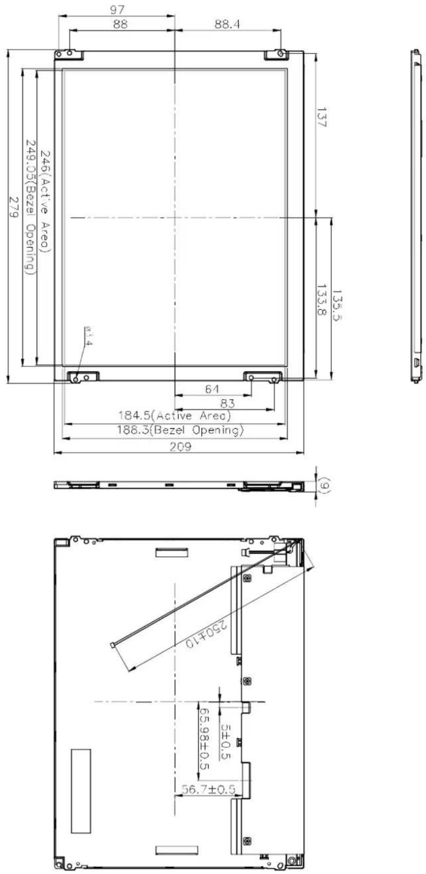
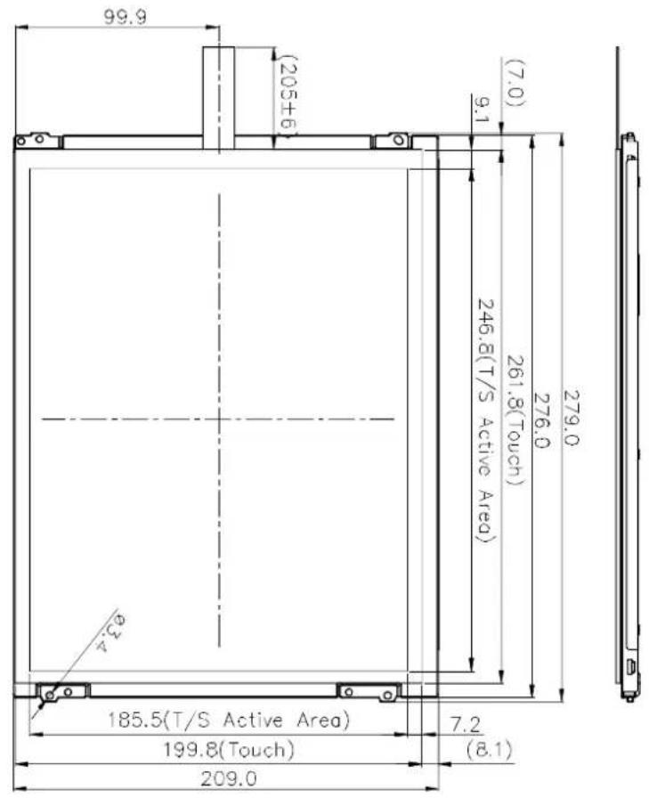
■ Dimensions (W x H x D): R series:279.0(H) x 209.0(V) x (11.3)(D) (Typ.)
N series:279.0(H) x 209.0(V) x (9.0)(D) (Typ.)
1.2.2 LED Driver Board
Efficiency: 90%
■ Output Current & Voltage: 400mA/18V
■ Dimensions (W x H x D): 62 x 16 x 6 mm
1.2.3 Touch Screen (R series)
■ Touch Screen: 5-Wire Resistive
■ Light Transmission: 80% ± 3%
■ Durability: 10 million times
1.2.4 Environment
Operating Temperature: -30\~85°C (IDK-2112N-K2SVA2E) / -20\~70°C (IDK-2112N/R-K2SVA2E)
Storage Temperature: -30\~85°C (IDK-2112N-K2SVA2E) / -25\~80°C (IDK-2112N/R-K2SVA2E)
■ Humidity: 95% @ 39°C, non-condensing
1.3 Mechanical Characteristics
IDK-2112N Series
IDK-2112R Series
text_image
99.9 (205±6) 9.1 (7.0) 246.8(T/S Active Area) 261.8(Touch) 279.0 185.5(T/S Active Area) 199.8(Touch) 7.2 (8.1) 209.0
natural_image
Technical line drawing of a mechanical component with dimension annotation (no text or symbols)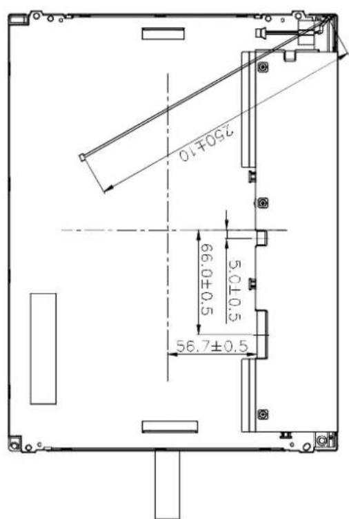
text_image
250±10 66.0±0.5 5.0±0.5 56.7±0.51.4 Functional Block Diagram
The following diagram shows the functional block of the 12.1 inches Color TFT-LCD Module:
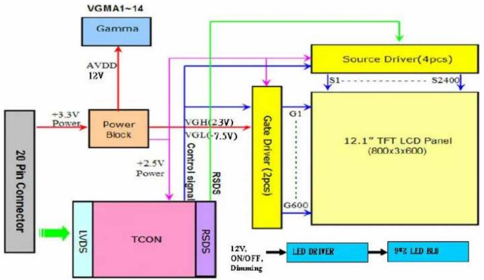
flowchart
graph TD
    A["20 Pin Connector"] -->|+3.3V Power| B["Power Block"]
    B --> C["TCON"]
    C --> D["Gate Driver (2pcs)"]
    D --> E["12.1" TFT LCD Panel (800x3x600)"]
    E --> F["Source Driver(4pcs)"]
    F --> G["S1 S2400"]
    G --> H["LED DRIVER"]
    H --> I["9*3 LED BLU"]
    J["VGMA1~14"] --> K["Gamma"]
    K --> L["AVDD 12V"]
    L --> M["Power Block"]
    M --> N["VGH(23V) VGL(-7.5V)"]
    N --> O["Gate Driver (2pcs)"]
    O --> P["G1"]
    P --> Q["G600"]
    Q --> R["LED DRIVER"]
    R --> S["9*3 LED BLU"]
    T["LVDS"] --> U["TCON"]
    U --> V["RSDS"]
    V --> W["VGH(23V) VGL(-7.5V)"]
    W --> X["Gate Driver (2pcs)"]
    X --> Y["G1"]
    Y --> Z["G600"]
    Z --> AA["LED DRIVER"]
    AA --> AB["9*3 LED BLU"]
    AC["Control signal"] --> AD["VGH(23V) VGL(-7.5V)"]
    AD --> AE["Gate Driver (2pcs)"]
    AE --> AF["G1"]
    AF --> AG["G600"]
    AG --> AH["LED DRIVER"]
    AH --> AI["9*3 LED BLU"]
Figure 1.1 Function block diagram
1.5 Absolute Maximum Ratings
Absolute maximum ratings of the module are as follows:
1.5.1 Absolute Ratings of TFT LCD Module
| Item Symbol Min. Max. Unit Conditions |
| Logic/LCD Drive Voltage Vin 0.3 +3.6 [Volt] Note 1, 2 |
1.5.2 Absolute Ratings of Backlight Unit
| Item Symbol Min. Max. Unit Conditions | ||||
| LED Light Bar Current | ILed | 800 | [mA] | Note 1, 2 |
1.5.3 Absolute Ratings of Environment
| Item | Symbol Min. Max. Unit | Conditions | ||
| Operating Temperature | TOP | -30 +85 | [°C] | for IDK-2112N-K2SVA2E only |
| -20 +70 | [°C] | |||
| Operation Humidity | HOP | 95 | [%RH] | Note 1 |
| Storage Temperature | TST | -30 +85 | [°C] | For IDK-2112N-K2SVA2E only |
| -25 +80 | [°C] | For IDK-2112R-K2SVA2E only | ||
| Storage Humidity | HST | 95 | [%RH] | Note 1 |
Note1: With in Ta= 39°C
Note2: Permanent damage to the device may occur if you exceed maximum values
Chapter 2
Electrical
Characteristics
2.1 Power Specification
Input power specifications are as follows:
| Table 2.1: Power specification | |||||||
| Symbol | Parameter | Min. | Typ. | Max. | Unit | ||
| VDD | Logic/LCD | 3.0 | 3.3 | 3.6 | [Volt] | 10% | |
| Drive Voltage | |||||||
| IDD | Input | Current | - | 280(VDD=3.3V, at 60Hz) | |||
| PDD | VDD Power | - | 0.924 | [Watt] | 64 Gray Bar Pattern(VDD=3.3V, at 60Hz) | ||
| IRush | Inrush Current | - | - | 1.5 | [A] | Note 1 | |
[mA]
Note1 Measurement condition:

text_image
(High to Low) Control Signal SW1 5W MAC-SPST +12.0V R2 1K C2 1uF/25V R1 47K Q3 AO6402 D6 D5 D2 D1 S F1 VDD (LCD Module Input) C1 1uF/16V G Q3 AO6402 C3 VR1 47K 0.01uF/25V 90% 10% 0V 470 us VDD rising time 3.3V 64 Gray pattern2.1.1 Signal Electrical Characteristics
Input signals shall be low or Hi-Z state when VDD is off.
| Table 2.2: Signal electrical characteristics | ||||||
| Symbol | Parameter | Min. | Typ. | Max. | Unit | Condition |
| VTH | Differential Input High Threshold | - | - | 100 | [mV] | VCM=1.2V |
| VTL | Differential Input Low Threshold | 100 | - | - | [mV] | VCM=1.2V |
| | VID | | Input Differential Voltage | 100 | 400 | 600 | [mV] | |
| VICM | Differential Input Common Mode Voltage | 1.1 | - | 1.45 [V] | VTH / VTL = ±100mV | |
Note LVDS Signal Waveform.

text_image
Single-end Signal Vp, Vn=|VID| > VTH = "High" VN VTH VTL | VID | Vp Vp, Vn=-|VID| < VTL = "Low" VCM GND Differential Signal | VID | VTH | VID | DTV VTL2.2 Backlight Driving Conditions
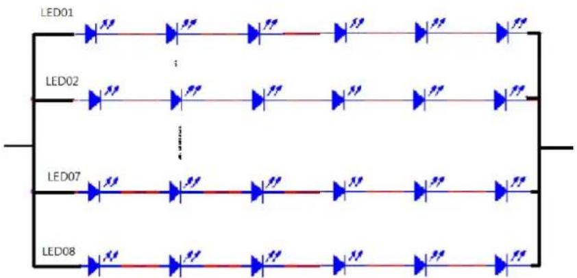
Parameter guideline for LED Light Bar Driver under stable conditions at 25^ C (Room Temperature):
Table 2.3: Backlight driving conditions
| Item Symbol Values Unit Condition | ||||||
| Min. | Typ. | Max. | ||||
| LED Voltage VL 18 V Note 2, 3 | ||||||
| LED Current IL 400 | mA | Note 2 | ||||
| LED life time | - | 50,000 | - | - | Hr | Note 1 |
Note1. The "LED life time" is defined as the module brightness decrease to 50% original brightness so that the ambient temperature is 25^ C and typical LED Current at 400mA.
Note 2. The LED driving condition is defined for each LED module (6 LED serial).
Note 3. The variance of LED Light Bar power consumption is 10%. To calculate a value use this for reference (IL x VL = PLED).
flowchart
graph TD
    LED01["LED01"] --> A1["Blue Arrow"]
    LED02["LED02"] --> A2["Blue Arrow"]
    LED07["LED07"] --> A3["Blue Arrow"]
    LED08["LED08"] --> A4["Blue Arrow"]
    A1 --> B1["Red Arrow"]
    A2 --> B2["Red Arrow"]
    A3 --> B3["Red Arrow"]
    A4 --> B4["Red Arrow"]
    B1 --> C1["Blue Arrow"]
    B2 --> C2["Blue Arrow"]
    B3 --> C3["Blue Arrow"]
    B4 --> C4["Blue Arrow"]
Chapter 3
Signal Characteristics
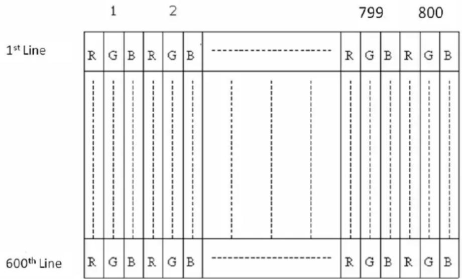
3.1 Pixel Format Image
The following figure shows the relationship between input signal and LCD pixel format.
3.2 Signal Description
Table 3.1: Symbol Description
| Pin No. Symbol Description | |||
| 1 VDD Power Supply, 3.3V (typical) | |||
| 2 VDD Power Supply, 3.3V (typical) | |||
| 3 GND Ground | |||
| 4 SEL68 6/ 8bits LVDS data input selection [H: 8bits L/NC: 6bit] | |||
| 5 | R | I | LVDS receiver signal channel 0 |
| 6 | R | I | LVDS Differential Data Input (R0, R1, R2, R3, R4, R5, G0) |
| 7 GND Ground | |||
| 8 | R | I | LVDS receiver signal channel 1 |
| 9 | R | I | LVDS Differential Data Input (G1, G2, G3, G4, G5, B0, B1) |
| 10 GND Ground | |||
| 11 RIN2- | LVDS receiver signal channel 2 | ||
| 12 RIN2+ | LVDS Differential Data Input (B2, B3, B4, B5, HS, VS, DE) | ||
| 13 GND Ground | |||
| 14 CLKIN- | LVDS receiver signal clock | ||
| 15 CLKIN+ | |||
| 16 GND Ground | |||
| 17 RIN3- LVDS receiver signal channel 3, NC for 6 bit LVDS Input | |||
| 18 RIN3+ | LVDS Differential Data Input (R6, R7, G6, G7, B6, B7, RSV) | ||
| 19 RSV Reverse Scan Function [H: Enable; L/NC: Disable] | |||
| 20 NC/GND Reserved for AUO internal test. Please treat it as NC. | |||
Note1 Input Signals shall be in low status when VDD is off.
Note2 High stands for "3.3V", Low stands for "0V", NC stands for "No Connection".
Note3 RSV stands for "Reserved".
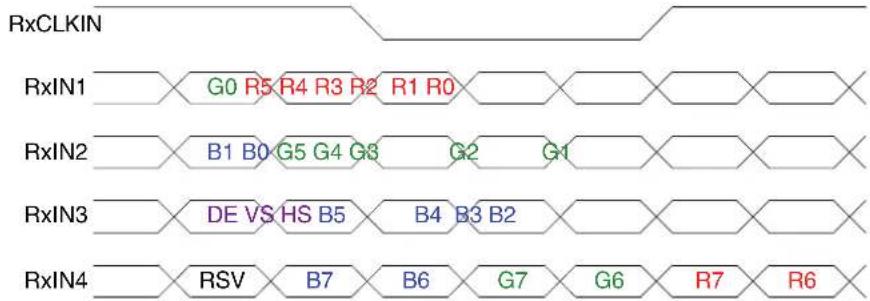
3.3 The Input Data Format
3.3.1 SEL68
SEL68 = "Low" or "NC" for 6 bits LVDS Input

flowchart
graph LR
    A["RxCLKIN"] --> B["RxIN1"]
    B --> C["G0 R5 R4 R3 R2 R1 R0"]
    C --> D[" "]
    D --> E["X"]
    F["RxIN2"] --> G["B1 B0 G5 G4 G3 G2 G1"]
    G --> H["X"]
    I["RxIN3"] --> J["DE VS HS B5 B4 B3 B2"]
    J --> K["X"]
SEL68 = "High" for 8 bits LVDS Input
flowchart
graph LR
    subgraph RxCLKIN
        A1["RxIN1"] --> B1["B1 B0"]
        B1 --> C1["G5 G4 G3"]
        C1 --> D1["G2 G1"]
        D1 --> E1["R7 R6"]
    end
    subgraph RxIN2
        A2["RxIN2"] --> B2["B2 B0"]
        B2 --> C2["G5 G4 G3"]
        C2 --> D2["G2 G1"]
        D2 --> E2["R7 R6"]
    end
    subgraph RxIN3
        A3["RxIN3"] --> B3["DE VS HS B5"]
        B3 --> C3["B4 B3 B2"]
        C3 --> D3["R7 R6"]
    end
    subgraph RxIN4
        A4["RxIN4"] --> B4["RSV B7"]
        B4 --> C4["B6 G7"]
        C4 --> D4["G6 R7"]
        D4 --> E4["R7 R6"]
    end
Note1: Please follow PSWG.
Note2: R/G/B data 7:MSB, R/G/B data 0:LSB
| Signal Name Description Remark | |
| +RED5(R5) Red Data 5 (MSB) | |
| +RED4(R4) Red Data 4 | |
| +RED3(R3) Red Data 3 | Red-pixel Data |
| +RED2(R2) Red Data 2 | Each red pixel's brightness data consists of these 6 bits pixel data. |
| +RED1(R1) Red Data 1 | |
| +RED0(R0) Red Data 0 (LSB) | |
| Red-pixel Data | |
| +GREEN5(G5) Green Data 5 (MSB) | |
| +GREEN4(G4) Green Data 4 | |
| +GREEN3(G3) Green Data 3 | Green-pixel Data |
| +GREEN2(G2) Green Data 2 | Each green pixel's brightness data consists of these 6 bits pixel data. |
| +GREEN1(G1) Green Data 1 | |
| +GREEN0(G0) Green Data 0 (LSB) | |
| Green-pixel Data | |
| +BLUE5(B5) Blue Data 5 (MSB) | |
| +BLUE4(B4) Blue Data 4 | |
| +BLUE3(B3) Blue Data 3 | Blue-pixel Data |
| +BLUE2(B2) Blue Data 2 | Each blue pixel's brightness data consists of these 6 bits pixel data. |
| +BLUE1(B1) Blue Data 1 | |
| +BLUE0(B0) Blue Data 0 (LSB) | |
| Blue-pixel Data | |
| CLK Data Clock The typical frequency is 40MHz. The signal is used to strobe the pixel data and DE signals. All pixel data shall be valid at the falling edge when the DE signal is high. | |
| DE Display Timing This signal is strobed at the falling edge of CLK. When the signal is high, the pixel data shall be valid to be displayed. | |
Note: Output signals from any system shall be low or Hi-Z state when VDD is off.
3.4 Interface Timing
3.4.1 Timing Characteristics
Table 3.2: Timing Characteristics
| Signal Symbol Min. Typ. Max. | Unit | |||||
| Clock frequency | 1/T_Clock | 34 | 40 | 48.3 | MHz | |
| Vertical Section | Period | T_V | 608 | 628 | 1024 | T_Line |
| Active | T_VD | - | 600 | - | ||
| Blanking | T_VB | 8 | 28 | 423 | ||
| Horizontal Section | Period | T_H | 960 | 1056 | 1060 | T_Clock |
| Active | T_HD | - | 800 | - | ||
| Blanking | T_HB | 220 | 256 | 440 | ||
Note1 Frame rate is 60 Hz.
Note2 DE mode.
3.4.2 Input Timing Diagram

text_image
CLK Tclk Input Data Invalid Data Pixel 1 Pixel 2 Pixel 3 Pixel M-1 Pixel M Invalid Data Pixel 1 Pixel 2 DE THB Tdisp(h) Th DE TVB Tdisp(v) Tv3.5 Power ON/OFF Sequence
VDD power and lamp on/off sequence is as follows. Interface signals are also shown in the chart. Signals from any system shall be Hi-Z state or low level when VDD is off.

text_image
VDD T1 T2 90% 10% T9 T10 T11 LVDS T3 90% T8 90% VCC 10% T4 T7 90% PWM Dimming 10% T5 T6 90% 10% Back Light ON/OFFPower Sequence Timing
| Parameter | Value | Unit | ||
| Min. | Typ. | Max. | ||
| T1 | 0.5 | - | 10 | [ms] |
| T2 | 30 | 40 | 50 | [ms] |
| T3 | 200 | - | - | [ms] |
| T4 | 10 | - | - | [ms] |
| T5 | 10 | - | - | [ms] |
| T6 | 0 | - | - | [ms] |
| T7 | 10 | - | - | [ms] |
| T8 | 100 - - [ms] | |||
T9 0 16 50 [ms]
T10 - - 10 [ms]
T11 1000 -- [ms]
The above on/off sequence should be applied to avoid abnormal functioning in the display. Please make sure to turn off the power when you plug the cable into the input connector or pull the cable out of the connector.
Chapter 4
Connector & Pin Assignment
4.1 TFT LCD Module
The physical interface connectors are capable of accommodating the following signals and components.
4.1.1 Connector
| Table 4.1: Connector |
| Connector Name / Description Signal Connector |
| Manufacture STM |
| Connector Model Number MSB240420-E |
| Adaptable Plug P240420 or compatible |
4.1.2 Pin Assignment
| Table 4.2: Pin Assignment | ||||
| Pin No. Signal Name Pin No. Signal Name | ||||
| 1 VDD 2 VDD | ||||
| 3 | G | N | D | 4 |
| 5 RIN0- | 6 RIN0+ | |||
| 7 | G | N | D | 8 |
| 9 RIN1+ | 10 | GND | ||
| 11 | RIN2- | 12 | RxIN2+ | |
| 13 | GND | 14 | CLKIN- | |
| 15 | CLKIN+ | 16 | GND | |
| 17 | RIN3- | 18 | RIN3+ | |
| 19 | RSV | 20 | NC/GND | |
4.2 Backlight Unit
These connectors are capable of accommodating the following signals and components.
| Connector Name / Designation | LED Light Bar Connector / Backlight lamp |
| Manufacturer | JST or compatible |
| Type Part Number | WF-SMT90 1.5mm Wire to board Heater |
4.2.1 Signal for LED light bar connector
| Connector No. | Pin No. | Input | Color | Function | |
| Lower | CN2 | 1 | HI 2 | Red | Power supply for backlight unit |
| 2 | GND 2 | Black | Ground for backlight unit |
Cable Length : 250mm+/-10mm
4.2.2 LED Driver Board
4.2.2.1 Specification:
Table 4.3: Specification
Symbol Characteristics Condition Min. Typ. Max. Unit
| Input | Voltage 11.2 12 13.2 V | ||||||
| Efficiency 90 | % | ||||||
| Output | Voltage | 17 | 18 | 19 | V | ||
| Current 380 | 400 | 420 | mA | ||||
| Current Accuracy | ±5 | % | |||||
| Protection | OVP, UVLO | ||||||
| Environment | Operating Temperature | -30 | 85 | °C | |||
| Storage Temperature | -40 | 105 | °C | ||||
| PWM Dim-mer | Dimmer range (Note. 1) | 5 | 100 | % | |||
| Dimmer VH | 5 | V | |||||
| Dimmer VL | 0 | V | |||||
| Dimmer Frequency | 0.5 | 40 KHz | |||||
| ON/OFF | Von | 3 | 5 | V | |||
| off | 0 | 0.8 | V | ||||

text_image
5% 95%Note1: When the input uses a PWM signal, the high-level digital output must be greater than the total output level of only 5% out.
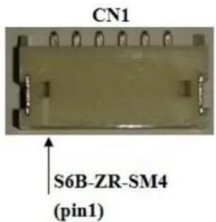
4.2.2.2 Input Connector Pin Definition
Table 4.4: Input Connector Pin Definition (CN1)
| Pin No. | Pin Definition |
| 1 | Vin(+12V) |
| 2 | Vin(+12V) |
| 3 | GND |
| 4 | GND |
| 5 | ON/OFF(ON:+3~5V, OFF=0~0.8V) |
| 6 | Dimming (PWM) |
text_image
CN1 S6B-ZR-SM4 (pin1)4.2.2.3 Output Connector Pin Definition
Table 4.5: Output Connector Pin Definition (CN4)
| Pin No. Pin Definition | |||
| 1 | V | L | E |
| 2 | V | L | E |
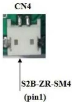
text_image
CN4 S2B-ZR-SM4 (pin1)4.2.2.4 Light Sensor Connector Pin Definition
Table 4.6: Light Sensor Connector Pin Definition (CN2)
| Pin No. Pin Definition |
| 1 Sensor High Voltage |
| 2 Sensor Low Voltage |

text_image
CN2 S2B-ZR-SM4 (pin1)4.2.2.5 Variable Resistor Connector Pin Definition
Table 4.7: Variable Resistor Connector Pin Definition (CN3)
| Pin No. Pin Definition | |
| 1 VR High Voltage | |
| 2 | VR |
| 3 VR Low Voltage | |
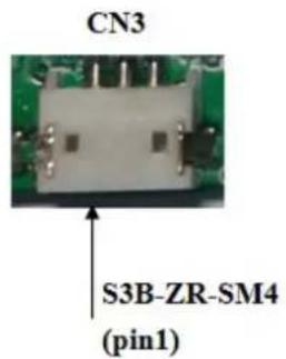
text_image
CN3 S3B-ZR-SM4 (pin1)4.2.2.6 Brightness Control Signal Flow Chart
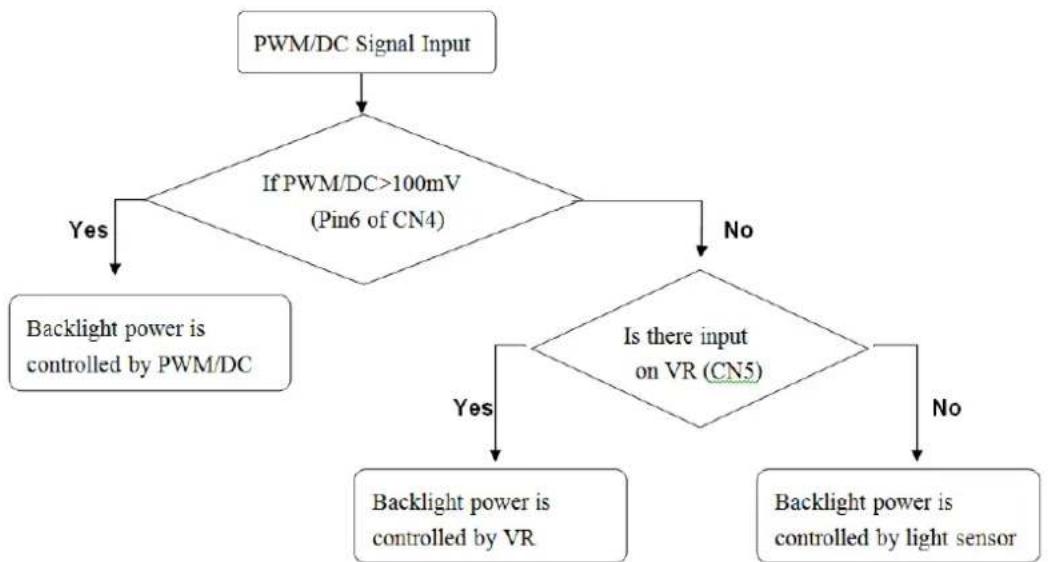
flowchart
graph TD
    A["PWM/DC Signal Input"] --> B{If PWM/DC>100mV (Pin6 of CN4)}
    B -->|Yes| C["Backlight power is controlled by PWM/DC"]
    B -->|No| D{Is there input on VR (CN5)}
    D -->|Yes| E["Backlight power is controlled by VR"]
    D -->|No| F["Backlight power is controlled by light sensor"]
Figure 4.1 Brightness Control Signal Flow Chart
4.2.2.7 Dimensions

text_image
13.0 mm 16.0 mm 0.0 mm QF531V2 TU <@> C3UC 9+UO E17L781(S) CN1 C5 0.0 mm 3.0 mm 0.0 mm 11.5 mm C16 U3 C6 R22 U2 φ3.0 mm φ3.0 mm 28.0 mm φ3.0 mm L1 U4 C7 D3 C4 62.0 mm -62.0 mm -16.0 mm -16.0 mm 0.0 mmFigure 4.2 Dimensions
Chapter 5
Touch Screen & Touch Controller
5.1 Touch Screen (Optional: for IDK-2112R only)
5.1.1 Touch Characteristics
The touch panel is a resistance type that customers use with flat displays like LCDs. Once an operator touches it, the circuit will send coordinate points to the PC from the voltage changes at the contact points.
5.1.2 Optical Characteristics
| Item Specification Remarks | ||||||||
| 1 TRANSPARENCY 80% ± 3% BYK-Gardner | ||||||||
| 2 | H | A | Z | E | 8 | . | 0 | ±3% BYK-Gardner |
5.1.3 Environment Characteristics
| Item Specification | Remarks | ||
| 1 | Operation temperature | -20°C ~ 70°C | Note: All terms under 1 atmosphere |
| 2 | Storage temperature | -40°C ~ 80°C | |
| 3 | Operation Humidity | 20% ~ 80%RH | |
| 4 | Storage temperature | 20% ~ 90%RH |
5.1.4 Mechanical Characteristics
| Item | Specification | Remarks | ||
| 1 | Hardness of surface | Pencil hardness 3H. | JIS K-5600-5-4150gf, 45 degree | |
| 2 | FPC peeling strength | 1) 5N (5N Min.)2) 19.6N (19.6N Min.) | 1) Peeling upward by 90°2) Peeling downward by 90° | |
| 3 | Operation force | Pen | 0.05N~1.96N(5~200gf) | Dot-SpacerWithin “guaranteed active area”, but not on the edge and Dot-Spacer. |
| Finger | ||||
5.1.5 Electronic Characteristics
| Item | Specification | Remarks | |
| 1 | Rated Voltage | DC 7V max. | |
| 2 | Resistance | X axis: 200Ω ~ 500Ω (Figure as below) | FPC connector |
| Y axis: 200Ω ~ 800Ω (Figure as below) | |||
| 3 | Linearity | X ≤1.5% (Figure as below) | Reference: 250gf |
| Y ≤1.5% (Figure as below) | |||
| 4 | Chattering | ≤ 15ms Max | |
| 5 | Insulation Resistance | ≥ 20MΩ min (DC 25V) |

text_image
RT LT LL RL LY LX5.1.6 General specification
| Item Specification | ||
| 1 | Frame size | 261.80±0.30 X 199.80±0.30 mm |
| 2 | View Area | 249.80±0.30 X 188.50±0.20 mm |
| 3 | Active Area | 246.80±0.30 X 185.50±0.20 mm |
| 4 Total Thickness | 2.20±0.20 mm | |
| 5 Tail length | 205.00±6.00 mm | |
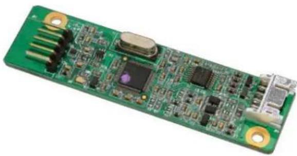
5.2 Touch controller (Optional: for IDK-2112R only)
Advantech ETM-RES04C Touch Control Board is the ultimate combo board. This touch panel controller provides optimum performance for your analog resistive touch panels for 5-wire models. Communication with the PC is directly through USB and RS-232 connector. The touch panel driver emulates mouse left and right button functions.
natural_image
Green printed circuit board with various electronic components and gold contacts (no visible text or symbols)5.2.1 Touch Controller Characteristics
5.2.1.1 Specifications
Electrical Features
+5 Vdc/ 100 mA typical, 50mV peak to peak maximum ripple and noise.
■ Bi-directional RS-232 serial communication and USB 1.1 full speed
■ Report rate of RS-232 is 180 points/sec (max.), USB is 200 points/sec (max.)
■ Unaffected by environmental EMI
Panel resistance of 5-wire resistive model is from 50 to 200 ohm (Pin to pin on same layer)
■ Touch resistance under 3K ohm
Serial Interface
EIA 232E (Serial RS-232)
■ No parity, 8 data bits, 1 stop bit, 9600 baud (N, 8, 1, 9600)
■ Support Windows 2000/ Vista/ XP/ 7, Windows CE 5.0/ 6.0/ 7.0, Windows NT4, Linux, DOS, QNX
USB Interface
■ Conforms to USB Revision 1.1 full speed.
If the USB is connected to the controller, the controller will communicate over the USB, and will not communicate over the serial port.
■ Supports Windows 2000/ Vista/ XP/ 7, Windows CE 5.0/ 6.0/ 7.0, Linux, QNX
Touch Resolution
■ 2,048 x 2,048 resolution
Response Time
Max. 20 ms
5.2.1.2 Environmental Feature
Reliability
■ MTBF is 200,000 hours
Temperature Ranges
■ Operating : -25°C \~ 85°C
■ Storage : -25°C \~ 85°C
Relative Humidity
■ 95% at 60°C, RH Non-condensing
Acquired RoHS certificate
Regulatory FCC-B, CE approvals
Dimension: 75 mm x 20 mm x 10 mm
5.2.2 Pin Assignment and Description
5.2.2.1 Connector and LED Location

text_image
JP1 Connector (USB&RS-232 Combo Interface) JP2 Connector (5-wire Touch screen Interface) LED5.2.2.2 Combo Interface Connector, JP1, Pins and signal descriptions
The combo interface connector, USB and RS-232, is a box 2.0mm 10-pins 90 degree, Male type with lock connector, intended to be used with single wired pins in 5+5 pins header. The pins are numbered as shown in the table below.
| USB Pin # | Signal Name | Signal Function RS-232 | Pin # | Signal Name | Signal Function |
| 1 G Ground | 1 G Ground | ||||
| 2 V USB Power | 2 V Power | ||||
| 3 G Ground | 3 G Ground | ||||
| 4 D+ USB | D+ 4 TxD Serial Port | ||||
| 5 D- | USB D- | 5 RxD | Serial Port | ||
| Signal Name | DB-9 pin # | RS-232 pin # | Sourced by | Signal Description |
| RxD | 2 | 5 | ctrl | serial data from controller to host |
| TxD | 3 | 4 | host | serial data from host to controller |
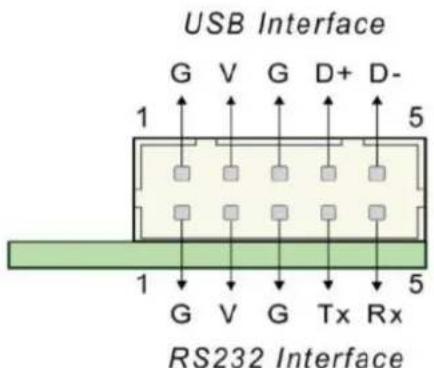
text_image
USB Interface G V G D+ D- 1 5 1 G V G Tx Rx RS232 InterfaceFigure 5.1 Board mounted header
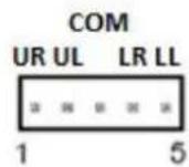
5.2.2.3 Touch Screen Connector, JP2, Pins and signal descriptions
The Touch Screen connector, JP2, is a single row by 2.54mm 5-pins 90 degree, Male type connector. The pins are numbered as shown in the table below.
| JP2 Pin # | Signal Name | Signal Description |
| 1 H / UR Drive signal attached to the touchscreen substrate upper right corner when viewed from a user's perspective. | ||
| 2 Y / UL | Drive signal attached to the substrate upper left corner. | |
| 3 COM | - | |
| 4 X / LR | Drive signal attached to the substrate lower right corner. | |
| 5 L / LL | Drive signal attached to the substrate lower left corner. | |


5.2.3 Physical dimension
ETM-RES04C-EEH4EE Touch Control Board (Unit: mm)
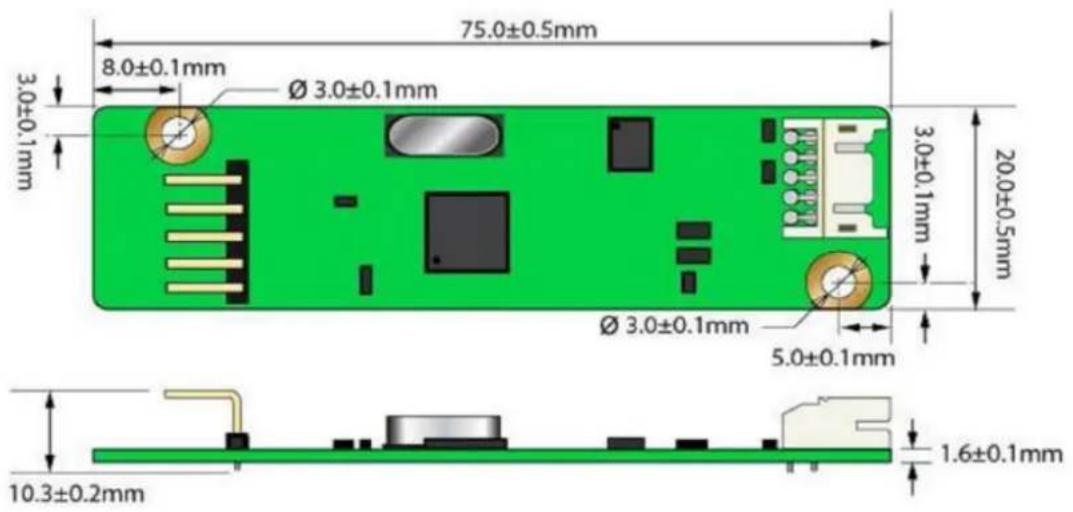
text_image
75.0±0.5mm 8.0±0.1mm Ø 3.0±0.1mm 3.0±0.1mm 20.0±0.5mm Ø 3.0±0.1mm 5.0±0.1mm 10.3±0.2mm 1.6±0.1mmAppendix A
Optical Characteristics
A.1 Test Conditions
| Item Symbol Value Unit | |||
| Ambient Temperature Ta | 25±2 | °C | |
| Ambient Humidity Ha | 50±10 | %RH | |
| Supply Voltage V | CC | 3.3 V | |
| Input Signal According to typical value in "3. ELECTRICAL CHARACTERISTICS" | |||
| Converter Voltage V | i | 12 | V |
| Converter Duty 100% | |||
A.2 Optical Specifications
The relative measurement methods of optical characteristics are shown below. The following items should be measured under the test conditions and stable environment shown in Note 5.
| Item | Conditions | Min. | Typ. | Max. | Unit | Remarks |
| White Luminance | I_F = 800mA/1 LEDLine (center point) | - | 1200 - | [cd/m2] Note 4 | ||
| Uniformity | 5 Points | 80 | - | - | % | Note 5, 6 |
| Contrast Ratio | 500 | 700 | - | Note 2 | ||
| Response Time | Rising | - | 25 | 35 | [msec] | Note 3 |
| Falling | - | 10 | 20 | [msec] | ||
| Raising + Falling | - | 35 | 55 | [msec] | ||
| Viewing Angle | Horizontal(Right) | 70 | 80 | - | [degree] | Note 1 |
| CR = 10 (Left) | 70 | 80 | - | [degree] | ||
| Vertical(Upper) | 55 | 65 | - | [degree] | ||
| CR = 10 (Lower) | 65 | 75 | - | [degree] | ||
| Color / Chromaticity Coordinates (CIE 1931) | Red x | 0.556 | 0.606 | 0.656 | ||
| Red y | 0.300 | 0.350 | 0.405 | |||
| Green x | 0.254 | 0.304 | 0.354 | |||
| Green y | 0.527 | 0.577 | 0.627 | |||
| Blue x | 0.099 | 0.149 | 0.199 | |||
| Blue y | 0.077 | 0.127 | 0.177 | |||
| White x | 0.263 | 0.313 | 0.363 | |||
| White y | 0.279 | 0.329 | 0.379 | |||
| Color Gamut | 55 | - | % |
Note 1 Definition of Viewing Angle ( _X , _Y )
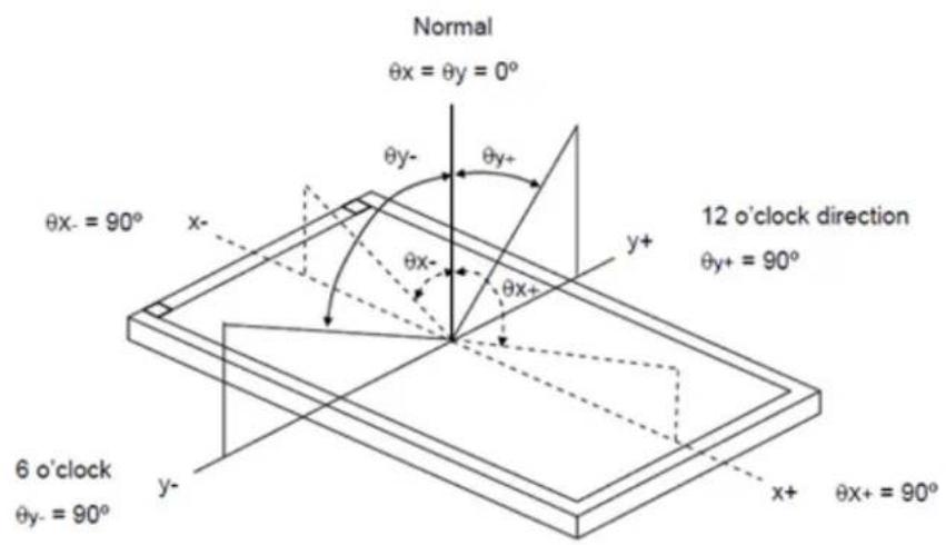
text_image
Normal θx = θy = 0° θy- θy+ θx- θx- θx+ 12 o'clock direction θy+ = 90° 6 o'clock θy- = 90° x+ θx+ = 90°Note 2 Definition of Contrast Ratio (CR):
The contrast ratio can be calculated by the following expression.
Contrast Ratio (CR) = L255 / L0
L255: Luminance of gray level 255
L0: Luminance of gray level 0
$$ C R = C R (5) $$
CR (X) is corresponding to the Contrast Ratio of the point X at Figure in Note 6.
Note 3 Definition of Response Time (TR, TF):

line
| Time Period | Optical Response | | --------------- | ---------------- | | Gray Level 255 | 100% | | Gray Level 0 | 0% | | Gray Level 255 | 100% |Note 4 Definition of Luminance of White (LC):
Measure the luminance of gray level 255 at center point
$$ \mathrm{LC} = \mathrm{L} (5) $$
L (x) is corresponding to the luminance of the point X at Figure in Note (6).
Note 5 Measurement Setup:
The LCD module should be stabilized at given temperature for 20 minutes to avoid abrupt temperature change during measuring. In order to stabilize the luminance, the measurement should be executed after the Backlight has been on for 20 minutes in a windless room.

text_image
LCD Module LCD Panel USB2000 Center of the Screen 500 mm CS-1000T Light Shield Room (Ambient Luminance < 2 lux)Note 6 Definition of White Variation ( W ):
Measure the luminance of gray level 255 at 5 points

other
| Position | Horizontal Line (D) | Vertical Line (W) | | : : Test Point; X=1 to 5 | | : Test Point; X=1 to 5 | | 1: Maximum [L(1), L(2), L(3), L(4), L(5)] | | 2: Maximum [L(1), L(2), L(3), L(4), L(5)] | | 3: Maximum [L(1), L(2), L(3), L(4), L(5)] | | 4: Maximum [L(1), L(2), L(3), L(4), L(5)] |Appendix B
Handling Precautions
B.1 Handling Precautions
The optical characteristics are measured under stable conditions at 25^ C (Room Temperature)
- Since the front polarizer is easily damaged, pay attention not to scratch it.
- Be sure to turn off power supply when inserting or disconnecting from the input connector.
- Wipe off water drops immediately. Long contact with water may cause discoloration or spots.
- When the panel surface is soiled, wipe it with absorbent cotton or other soft cloth.
- Since the panel is made of glass, it may break or crack if dropped or bumped on hard surface.
- Since CMOS LSI is used in this module, take care of static electricity and insure human earth when handling.
- Do not open or modify the module assembly.
- Do not press the reflector sheet at the back of the module in any directions.
- In case a module has to be put back into the packing container slot after it was taken out from the container, please press the far ends of the LED light bar reflector edge softly. Otherwise the TFT Module may be damaged.
- At the insertion or removal of the Signal Interface Connector, be sure not to rotate nor tilt the Interface Connector of the TFT Module.
- After installation of the TFT module into an enclosure, do not twist nor bend the TFT module even momentary. At designing the enclosure, it should be taken into consideration that no bending/twisting forces are applied to the TFT module from outside. Otherwise the TFT module may be damaged.
- Small amount of materials having no flammability grades are used in the LCD module. The LCD module should be supplied with power complying with requirements of Limited Power Source (IEC60950 or UL1950), or have applied for exemption.
www.advantech.com
Please verify specifications before quoting. This guide is intended for reference purposes only.
All product specifications are subject to change without notice.
No part of this publication may be reproduced in any form or by any means, electronic, photocopying, recording or otherwise, without prior written permission of the publisher.
All brand and product names are trademarks or registered trademarks of their respective companies.
© Advantech Co., Ltd. 2015