TC1321 - Carte de démonstration Microchip - Free user manual and instructions
Find the device manual for free TC1321 Microchip in PDF.

User questions about TC1321 Microchip
0 question about this device. Answer the ones you know or ask your own.
Ask a new question about this device
Download the instructions for your Carte de démonstration in PDF format for free! Find your manual TC1321 - Microchip and take your electronic device back in hand. On this page are published all the documents necessary for the use of your device. TC1321 by Microchip.
USER MANUAL TC1321 Microchip
Note the following details of the code protection feature on Microchip devices:
• Microchip products meet the specification contained in their particular Microchip Data Sheet.
- Microchip believes that its family of products is one of the most secure families of its kind on the market today, when used in the intended manner and under normal conditions.
- There are dishonest and possibly illegal methods used to breach the code protection feature. All of these methods, to our knowledge, require using the Microchip products in a manner outside the operating specifications contained in Microchip's Data Sheets. Most likely, the person doing so is engaged in theft of intellectual property.
• Microchip is willing to work with the customer who is concerned about the integrity of their code.
- Neither Microchip nor any other semiconductor manufacturer can guarantee the security of their code. Code protection does not mean that we are guaranteeing the product as "unbreakable."
Code protection is constantly evolving. We at Microchip are committed to continuously improving the code protection features of our products. Attempts to break Microchip's code protection feature may be a violation of the Digital Millennium Copyright Act. If such acts allow unauthorized access to your software or other copyrighted work, you may have a right to sue for relief under that Act.
Information contained in this publication regarding device applications and the like is provided only for your convenience and may be superseded by updates. It is your responsibility to ensure that your application meets with your specifications. MICROCHIP MAKES NO REPRESENTATIONS OR WARRANTIES OF ANY KIND WHETHER EXPRESS OR IMPLIED, WRITTEN OR ORAL, STATUTORY OR OTHERWISE, RELATED TO THE INFORMATION, INCLUDING BUT NOT LIMITED TO ITS CONDITION, QUALITY, PERFORMANCE, MERCHANTABILITY OR FITNESS FOR PURPOSE. Microchip disclaims all liability arising from this information and its use. Use of Microchip's products as critical components in life support systems is not authorized except with express written approval by Microchip. No licenses are conveyed, implicitly or otherwise, under any Microchip intellectual property rights.
Trademarks
The Microchip name and logo, the Microchip logo, Accuron, dsPIC, KEELOQ, microID, MPLAB, PIC, PICmicro, PICSTART, PRO MATE, PowerSmart, rfPIC, and SmartShunt are registered trademarks of Microchip Technology Incorporated in the U.S.A. and other countries.
AmpLab, FilterLab, Migratable Memory, MXDEV, MXLAB, PICMASTER, SEEVAL, SmartSensor and The Embedded Control Solutions Company are registered trademarks of Microchip Technology Incorporated in the U.S.A.
Analog-for-the-Digital Age, Application Maestro, dsPICDEM, dsPICDEM.net, dsPICworks, ECAN, ECONOMONITOR, FanSense, FlexROM, fuzzyLAB, In-Circuit Serial Programming, ICSP, ICEPIC, MPASM, MPLIB, MPLINK, MPSIM, PICkit, PICDEM, PICDEM.net, PICLAB, PICtail, PowerCal, PowerInfo, PowerMate, PowerTool, rfLAB, rfPICDEM, Select Mode, Smart Serial, SmartTel and Total Endurance are trademarks of Microchip Technology Incorporated in the U.S.A. and other countries.
SQTP is a service mark of Microchip Technology Incorporated in the U.S.A.
All other trademarks mentioned herein are property of their respective companies.
© 2004, Microchip Technology Incorporated, Printed in the U.S.A., All Rights Reserved.

Printed on recycled paper.
QUALITY MANAGEMENT SYSTEM
CERTIFIED BY DNV
=ISO/TS 16949:2002=
Microchip received ISO/TS-16949:2002 quality system certification for its worldwide headquarters, design and wafer fabrication facilities in Chandler and Tempe, Arizona and Mountain View, California in October 2003. The Company's quality system processes and procedures are for its PICmicro® 8-bit MCUs, KEELOC® code hopping devices, Serial EEPROMs, microperipherals, nonvolatile memory and analog products. In addition, Microchip's quality system for the design and manufacture of development systems is ISO 9001:2000 certified.
Table of Contents
Preface 1
Chapter 1. Product Overview....5
1.1 Introduction ...... 5
1.2 Purpose and Utility of the Mixed Signal PICtail™ Demo Board 5
1.3 Contents of the Mixed Signal PICtail™ Demo Board Kit 5
Chapter 2. Installation and Operation ....7
2.1 Introduction 7
2.2 Features 7
2.3 Getting Started 7
2.4 Running the demos 13
Appendix A. Schematics and Layouts ...... 17
A.1 Introduction 17
Appendix B. Bill-Of-Materials (BOM) 25
Appendix C. MixedSignal\_V100.asm Description 27
Appendix D. DAC\_dtmf.asm Source Code 29
Appendix E. MixedSignal\_16f767i.Ikr Source Code 39
Appendix F. DTMF Scope Captures 41
Appendix G. Scope Probe Noise Captures 43
Appendix H. Sine Wave and Filtered DTMF Scope Captures 45
Appendix I. MPLAB ^® IDE Screen Capture 47
Worldwide Sales and Service 48
NOTES:
Preface
NOTICE TO CUSTOMERS
All documentation becomes dated, and this manual is no exception. Microchip tools and documentation are constantly evolving to meet customer needs, so some actual dialogs and/or tool descriptions may differ from those in this document. Please refer to our web site (www.microchip.com) to obtain the latest documentation available.
Documents are identified with a "DS" number. This number is located on the bottom of each page, in front of the page number. The numbering convention for the DS number is "DSXXXXXA", where "XXXXX" is the document number and "A" is the revision level of the document.
For the most up-to-date information on development tools, see the MPLAB ^® IDE on-line help. Select the Help menu, and then Topics to open a list of available on-line help files.
INTRODUCTION
This chapter contains general information that will be useful to know before using the Mixed Signal PICtail™ Demo Board. Items discussed in this chapter include:
- About This Guide
- Conventions Used in this Guide
- Recommended Reading
• The Microchip Web Site - Customer Support
ABOUT THIS GUIDE
Document Layout
This document describes how to use the Mixed Signal PICtail™ Demo Board. The manual layout is as follows:
- Chapter 1. Product Overview – Important information about the Mixed Signal PICtail™ Demo Board.
- Chapter 2. Installation and Operation – Includes instructions on how to get started with this demo board and a detailed description of each function of the demo board.
- Appendix A. Schematics and Layouts – Shows the schematic and layout diagrams for the Mixed Signal PICtail™ Demo Board.
- Appendix B. Bill-Of-Materials (BOM) – Lists the parts used to build the Mixed Signal PICtail™ Demo Board.
- Appendix C. MixedSignal_V100.asm Description – Example "Main" assembly firmware for the PIC16F767-I/SS microcontroller used to demonstrate the various features of the supported analog products.
- Appendix D. DAC_dtmf.asm Source Code – Example assembly source firmware used to generate Dual Tone Multiple Frequency (DTMF) signals. This firmware is utilized by the "Main" firmware, MixedSignal_v100.ASM.
- Appendix E. MixedSignal_16f767i.Ikr Source Code – Linker script file used to build the example PIC16F767 firmware.
- Appendix F. DTMF Scope Captures – Oscilloscope screen captures of the various DTMF tones displaying their FFT to illustrate the quality of the DTMF tones.
- Appendix G. Scope Probe Noise Captures – Isolating scope probe noise is challenging. These scope captures illustrate the difference between using a standard scope probe and using coaxial cable directly from the board into the scope.
- Appendix H. Sine Wave and Filtered DTMF Scope Captures – Oscilloscope screen capture of the 32-step sine wave routine and the DTMF waveform. The DTMF waveform illustrates the non-filtered DAC output and a simple RC-filtered output.
- Appendix I. MPLAB® IDE Screen Capture – MPLAB IDE 6.3x was used to generate the example source firmware. This screen capture illustrates the tool, the project files and the included Watch windows.
CONVENTIONS USED IN THIS GUIDE
This manual uses the following documentation conventions:
DOCUMENTATION CONVENTIONS
| Description Represents Examples | ||
| Arial font: | ||
| Italic characters Referenced books | MPLAB | ^ IDE User's Guide |
| Emphasized text ...is the only compiler... | ||
| Initial caps A window the Output | window | |
| A dialog the Settings dialog | ||
| A menu selection select Enable | Programmer | |
| Quotes A field name in a window or dialog | "Save project before build" | |
| Underlined, italic text with right angle bracket | A menu path File>Save | —— |
| Bold characters A dialog button | Click OK | |
| A tab | Click the Power tab | |
| 'bnnnn | A binary number where n is a digit | 'b00100, 'b10 |
| Text in angle brackets <> | A key on the keyboard | Press,, |
| Courier font: | ||
| Plain Courier | Sample source code | #define START |
| Filenames | autoexec.bat | |
| File paths | c:\mcc18\h | |
| Keywords | _asm, _endasm, static | |
| Command-line options | -Opa+, -Opa- | |
| Bit values | 0, 1 | |
| Italic Courier | A variable argument | file.o, where file can be any valid filename |
| 0xnnnn A hexadecimal number where n is a hexadecimal digit | 0xFFFF, 0x007A | |
| Square brackets [] | Optional arguments | mccl8 [options] file [options] |
| Curly brackets and pipe character: { | } | Choice of mutually exclusive arguments; an OR selection | errorlevel {0|1} |
| Ellipses... Replaces repeated text var_name [, | var_name...] | |
| Represents code supplied by user | void main (void) { ... } | |
RECOMMENDED READING
This user's guide describes how to use the Mixed Signal PICtail™ Demo Board. Other useful documents are listed below. The following Microchip documents are available and recommended as supplemental reference resources.
MCP4921/22, "12-Bit DAC with SPI™ Interface" Data Sheet (DS21897)
Provides detailed information regarding the MCP492X devices.
TC1320, "8-Bit Digital-to-Analog Converter with Two-Wire Interface" Data Sheet (DS21386)
Provides detailed information regarding the TC1320 device.
TC1321, "10-Bit Digital-to-Analog Converter with Two-Wire Interface" Data Sheet (DS21387)
Provides detailed information regarding the TC1321 device.
MCP3302/3304, "13-Bit Plus Sign Differential Input 2.7V Low-Power A/D Converter with SPI™ Serial Interface" Data Sheet (DS21697)
Provides detailed information regarding the MCP3302 and MCP3304 devices.
MCP3204/3208, "2.7V 12-Bit A/D Converters with SPI™ Serial Interface" Data Sheet (DS21298)
Provides detailed information regarding the MCP3204 and MCP3208 devices.
MCP1525/1541, "2.5V and 4.096V Voltage Reference" Data Sheet (DS21653)
Provides detailed information regarding the MCP1525 and MCP1541 devices.
TC55, "1 μA Low-Dropout Positive Voltage Regulator" Data Sheet (DS21653)
Provides detailed information regarding the TC55 device.
MCP1700, "Low-Quiescent Current LDO" Data Sheet (DS21826)
Provides detailed information regarding the MCP1700 device.
MCP616/617/618/619, "2.3V to 5.5V Micropower Bi-CMOS Op Amps" Data Sheet (DS21613)
Provides detailed information regarding the MCP616, MCP617, MCP618 and MCP619 devices.
PIC16F737, PIC16F747, PIC16F767, PIC16F777, "PIC16F7X7 Data Sheet" (DS30498)
Provides detailed information regarding the PIC16F737, PIC16F747, PIC16F767 and PIC16F777 devices.
Microchip provides online support via our web site at www.microchip.com. This web site is used as a means to make files and information easily available to customers. Accessible by using your favorite Internet browser, the web site contains the following information:
- Product Support – Data sheets and errata, application notes and sample programs, design resources, user's guides and hardware support documents, latest software releases and archived software
- General Technical Support – Frequently Asked Questions (FAQ), technical support requests, online discussion groups and Microchip consultant program member listing
- Business of Microchip – Product selector and ordering guides, latest Microchip press releases, listing of seminars and events, listings of Microchip sales offices, distributors and factory representatives
CUSTOMER SUPPORT
Users of Microchip products can receive assistance through several channels:
• Distributor or Representative
- Local Sales Office
• Field Application Engineer (FAE)
- Technical Support
- Development Systems Information Line
Customers should contact their distributor, representative or field application engineer (FAE) for support. Local sales offices are also available to help customers. A listing of sales offices and locations is included in the back of this document.
Technical support is available through the web site at: http://support.microchip.com In addition, there is a Development Systems Information Line which lists the latest versions of Microchip's development systems software products. This line also provides information on how customers can receive currently available upgrade kits.
The Development Systems Information Line numbers are:
1-800-755-2345 – United States and most of Canada
1-480-792-7302 – Other International Locations
NOTES:
Chapter 1. Product Overview
1.1 INTRODUCTION
This chapter provides an overview of the Mixed Signal PICtail™ Demo Board and covers the following topics:.
- Purpose and utility of the Mixed Signal PICtail™ Demo Board
- Contents of the Mixed Signal PICtail™ Demo Board Kit
1.2 PURPOSE AND UTILITY OF THE MIXED SIGNAL PICtail™ DEMO BOARD
The Mixed Signal PICtail™ Demo Board allows the system designer to quickly evaluate the suitability of several Microchip analog products for their product's design. Microchip's Digital-to-Analog Converters (DACs), Analog-to-Digital Converters (ADCs), V_REF , Low Dropout Output (LDO) regulators and the PIC16F7X7 devices are supported. Evaluating precision analog products for specific applications can be challenging for practical reasons. First, many products are only available in surface-mount packages. Secondly, analog circuits tend to be affected adversely by system noise. Common breadboarding techniques are not practical for these reasons. The Mixed Signal PICtail™ Demo Board utilizes a 4-layer Printed Circuit Board (PCB), with attention paid to reducing system noise.
The Mixed Signal PICtail™ Demo Board can isolate a specific device's performance to establish baseline performance. The board can be customized quickly for specific system requirements.
1.3 CONTENTS OF THE MIXED SIGNAL PICtail DEMO BOARD KIT
This Mixed Signal PICtail™ Demo Board includes:
• The Mixed Signal PICtail™ Demo Board PCB
- PIC16F767 firmware that demonstrates how to configure and write to the MCP492X, MCP482X and TC132X DAC products
- PIC16F767 firmware demonstrating DTMF generation using a DAC
- PIC16F767 firmware demonstrating sine-wave generation using a DAC
- PIC16F767 firmware to configure and read the MCP330X/320X SAR ADCs
- PIC16F767 firmware that configures and reads the MCP3551 Sigma-Delta ADC
- MCP617 dual op amp (standard 8-pin dual layout) that can be configured as an input signal filter (ADC) or an output signal conditioning stage for the DACs
- Four DIP switches allow simple firmware mode selection
- Two indicator LEDs (red and green) for visual feedback
- PICkit™ 1 Flash Starter Kit's 14-pin header provides an interface to Microchip's 8- and 14-pin PICmicro® microcontroller devices
NOTES:
Chapter 2. Installation and Operation
2.1 INTRODUCTION
The Mixed Signal PICtail™ Demo Board demonstrates several Microchip analog products in a signal chain configuration. The product families demonstrated include DACs, ADCs, VREFs, LDOs and PICmicro® microcontroller devices. Evaluating precision analog products for specific applications can be challenging due to noise sources related to the PCB layout and not the silicon under evaluation. The Mixed Signal PICtail™ Demo Board provides the necessary hardware and firmware to exercise each of these devices in real-world applications. Users can quickly modify the existing hardware and firmware to validate functionality for their specific system needs.
2.2 FEATURES
The Mixed Signal PICtail™ Demo Board has the following features:
- Printed Circuit Board (PCB) is a 4-layer board designed to minimize external noise
- A 28-pin PICmicro (PIC16F767) microcontroller footprint is provided to permit code development. In-Circuit Debugger is supported via the RJ11 connector
- The 14-pin header is designed to seamlessly interface to the PICkit™ 1 Flash Starter Kit
- Firmware demonstrating DTMF generation on the MCP492X/482X DAC is included
- Firmware demonstrating a precision sine-wave generation on the TC132X DAC is included
- Firmware to configure and read the MCP330X/320X SAR ADCs is included
- Two precision voltage references (V _REFs ) are supported (can compare noise)
- Flexible amplifier circuit layout supports a dual op amp in multiple configurations for either an input signal filter (ADC) or an output signal-conditioning stage for the DACs
- Four DIP switches allow simple firmware mode selection are supported
- Two indicator LEDs (red and green) are supported
- Can be powered by either the PICkit™ 1 Flash Starter Kit or by an external 9V supply
2.3 GETTING STARTED
The Mixed Signal PICtail™ Demo Board is assembled and tested for evaluation and demonstration of the MCP492X, MCP482X, TC132X, MCP3551, MCP3302, MCP3204, MCP1541, MCP1701, PIC16F767 and MCP617 features. Additional product samples with footprints supported by this board are included. A block diagram of the demo board is shown in Figure 2-1. Refer to Appendix A. "Schematics and Layouts" and Appendix B. "Bill-Of-Materials (BOM)" for more detailed circuit information.

flowchart
graph TD
    A["TC55 (10V VIN)\nMCP1701 (10V VIN)\nMCP1700 (<6V VIN)"] --> B["U1"]
    C["Mode Switch"] --> D["S1"]
    D --> E["PICmicro®\nMCU\nPIC16F767"]
    E --> F["CS0"]
    E --> G["CS1"]
    F --> H["MPLAB® ICD Header\n(for debugging and programming)"]
    G --> I["MPLA1541\nMCP1525 VREF"]
    J["U9"] --> K["REF198G VREF"]
    L["U5 & U10"] --> M["MCP4821 DAC\nMCP4822 DAC\nMCP4921 DAC\nMCP4922 DAC"]
    M --> N["SPI™"]
    N --> O["VOUTA"]
    N --> P["VOUTB"]
    Q["U7"] --> R["TC1320 DAC\nTC1321 DAC"]
    R --> S["VOUTC"]
    R --> T["I²CTM"]
    U["U12"] --> V["MCP617 Dual Op Amp"]
    W["J1, J2, J3"] --> X["PICkit™ 1 Flash Starter Kit Header"]
    X --> Y["5"]
    Z["J4"] --> AA["MPLAB® ICD Header"]
    AA --> AB["(for debugging and programming)"]
FIGURE 2-1: Mixed Signal PICtail™ Demo Board Block Diagram.
2.3.1 The Hardware
Figure 2-2 shows the layout of the Mixed Signal PICtail™ Demo Board with indicators to points of interest, while Table 2-1 details the PICkit™ 1 Flash Starter Kit Header connections. Jumpers JP1-JP5 are fully described in Section 2.3.2 "The Embedded System Firmware".
text_image
MCP3551-I/MS 22-Bit ADC Analog Devices REF198G 4.096V Voltage Reference MCP3551-I/P 22-Bit ADC JP4a ADC VREF Source Selector VOUTD SMA Connector MCP617-I/SN Dual Op Amp (can be any dual or single op amp using the standard footprint) MCP3302-I/SL 13-Bit Differential SPI™ ADC MCP3204-I/SL 12-Bit Single-ended SPI™ ADC JP2 VOUTA Selector JP1 VOUTC Selector PIC16F767-I/SS 28-pin Flash PICmicro® Microcontroller with Internal Oscillator Red and Green LEDs Mixed Signal Bd. 102-00027 Mode Selector DIP switches TC55RP5002 5.0V LDO (10V VIN) MCP1701T-5002I/CB 5.0V LDO (10V VIN) MCP1700T-5002I/CB 5.0V LDO (6V VIN)FIGURE 2-2: Mixed Signal PICtail™ Demo Board.
TABLE 2-1: PICkit™ 1 FLASH STARTER KIT 14-PIN HEADER INTERFACE PINS
| Pin Name | Pin Number | Pin Type | Buffer Type | Description |
| V_SS | 14 — | — Electrical Grou | nd. Both analog and digital. | |
| V_IN | 13 | — | — | Power Supply Input. Refer to Note 2 in Appendix A “Schematics and Layouts”. Do not plug in 9V supply and connect to PICkitTM 1 Flash Starter Kit. |
| CS0 12 O — | SPITM Chip Select signal for the external ADCs. Do not populate both the MCP3551 and the MCP3302 as they share the same CS0 signal. | |||
| SCK/SCL 11 | O ST SPI Clock or I | ^2C^TM Clock Signal. Note that external weak pull-up R_20 connects this signal to V_DD2 . | ||
| SDI/SDA 10 | I/O | ST | SPI Data | In or I ^2C Data signal (Data Out on ADC). Note that external weak pull-up R_14 connects this signal to V_DD2 . |
| SDO | 9 | O — | SPI Data | Out Signal (Data In on DAC and ADC) |
| CS1 | 8 | O — | SPI Chip | Select Signal for the External DACs. Do not populate both the MCP492X and the MCP482X as they share the same CS0 signal. |
| LDAC | 7 | O — | Latches | the DAC Output When Low. Note the weak pull-down resistor R_5 if the firmware doesn't drive the pin to a desired state. |
| V_REF\_ADC | 6 | I — | JP4 selects the V _REF source to use as the ADC reference signal. The PICmicro® microcontroller on the PICkitTM 1 Flash Starter Kit may use this for its internal ADC's V_REF . | |
| LED0/TX | 5 | O — | Active High Red LED Signal. This I/O also has the USART's TX signal multiplexed on it. | |
| LED1/RX | 4 | I/O | — | Active High Green LED Signal. This I/O also has the USART's RX signal multiplexed on it. |
| SW0 | 3 | I — | S1's Switch 1. This pin uses the internal pull-up resistor to determine when the switch is open. | |
| SW1 | 2 | I — | S1's Switch 2. This pin uses the internal pull-up resistor to determine when the switch is open. | |
| SW2 | 1 | I — | S1's Switch 3. This pin uses the internal pull-up resistor to determine when the switch is open. | |
Legend: TTL = TTL compatible input ST = Schmitt Trigger input with CMOS levels I = Input O = Output
2.3.2 The Embedded System Firmware
The Mixed Signal PICtail™ Demo Board firmware utilizes PICmicro® microcontroller assembly language, Microchip MPASM™ assembler and MPLINK™ linker to build the. HEX machine file. MixedSignal_v100.asm, DAC_dtmf.asm, p16F767.inc and MCP492X_16f767i.lkr files are needed in your project to build the MixedSignalPICtail.hex.
MixedSignal_v100.asm contains the main program and most of the subroutines. After initialization of critical PICmicro microcontroller peripherals (including the internal oscillator to 8 Mhz), the main loop polls the four DIP switches to determine the selected mode of operation. The DIP switches create a 4-bit binary number from 0 to 15. If a change of mode is detected for 100 ms during 500 ms of scanning, a new mode is selected and the LEDs are alternately flashed for two seconds. Most of the modes will time-out and re-scan the DIP switches periodically.
Refer to Appendix C. "MixedSignal_V100.asm Description" for the commented source code further describing each mode.
Modes 0XXX primarily utilize the MCP492X DAC modes:
- Mode0000: Use the DTMF generation subroutine (located in DAC_dtmf.asm) to dial a phone number stored in memory. Analyze output on V_OUTB or V_OUTD 's SMA connector. See Appendix F. "DTMF Scope Captures" for resulting waveform frequency analysis.
- Mode0001: Send 000h and FFFh commands to generate a 100 Hz R-R output on the MCP492X. Probe V_OUTA and V_OUTB to see the resulting waveforms.
- Mode0010: Send 400h and BFFh commands to generate a 100 Hz output on the MCP492X. Probe V_OUTA and V_OUTB to see the resulting waveforms.
- Mode0011: DACA = SHDN, DACB = SHDN, PIC = SLEEP. This mode demonstrates the low-power nature of the DAC, the PICmicro microcontroller, the op amp and the LDO. A power cycle is required after the mode switch is changed to exit this mode.
- Mode0100: DACB and DACA = 800h and Read w/PIC16F767 10b ADC, "broadcast on USART". This mode is useful for evaluating the PICmicro microcontroller's ADC. A _IN_B can be injected with an alternative signal and the result can be analyzed through the 19200 baud async, 9-bit transmission. Microchip's Data View analysis tool, along with the MCP3551 USB evaluation board, provide a "canned" analysis solution.
- Mode0101: DACB = 801h, DACA = 800h and Read w/MCP3302 13b Dif, "broadcast on USART". This mode is useful for evaluating the MCP3302 or the MCP3204 ADC. A _IN_B can be injected with an alternative signal and the result can be analyzed through the 19200 baud async, 9-bit transmission. Microchip's Data View analysis tool, along with the MCP3551 USB evaluation board, provide a "canned" analysis solution.
- Mode0110: DACB and DACA = 800h and Read w/MCP3551, "broadcast on USART". This mode is useful for evaluating the MCP3551 ADC or the MCP1541 VREF. AIN_B can be injected with an alternative signal and the result can be analyzed through the 19200 baud async, 9-bit transmission. Microchip's Data View analysis tool, along with the MCP3551 USB evaluation board, provide a "canned" analysis solution.
- Mode0111: Open for user to define their own routine.
Modes 1XXX primarily utilize TC132X DAC modes:
- Mode1000: Generate a 100 Hz 32-step sine wave on the TC132X. Analyze output on V_OUTC . See Appendix H. "Sine Wave and Filtered DTMF Scope Captures" for resulting unfiltered waveform.
- Mode1001: Send 000h and FFFh commands to generate a 100 Hz R-R output on the TC132X. Probe V_OUTC to see the resulting waveforms.
- Mode1010: Send 400h and BFFh commands to generate a 100 Hz output on the TC132X. Probe VOUTC to see the resulting waveforms.
- Mode1011: DAC = SHDN, PIC = SLEEP. This mode demonstrates the low-power nature of the DAC, the PICmicro microcontroller, the op amp and the LDO. A power cycle is required after the mode switch is changed to exit this mode.
- Mode1100: DAC = 200h and Read with PIC16F767 10b ADC, "broadcast on USART". AIN_C can be analyzed using Microchip's Data View analysis tool, which, along with the MCP3551 USB evaluation board, provides a "canned" analysis solution.
- Mode1101: DAC = 200h and Read with MCP3302 13b single-ended, "broadcast on USART". A _IN_C can be analyzed using Microchip's Data View analysis tool, which, along with the MCP3551 USB evaluation board, provides a "canned" analysis solution.
- Mode1110: Open for user to define their own routine.
- Mode1111: Open for user to define their own routine.
Refer to Appendix C. "MixedSignal_V100.asm Description" to view source code and comments.
Refer to Appendix D. "DAC_dtmf.asm Source Code" to view source code and comments.
Refer to Appendix E. "MixedSignal_16f767i.Ikr Source Code" to view the script.
Refer to the p16F767.inc standard include file located in your "\MPLAB IDE\MCHIP_Tools\" folder.
2.4 RUNNING THE DEMOS
The Mixed Signal PICtail™ Demo Board was designed to utilize the PIC16F767 located on the PCB or a PICmicro microcontroller operating on the PICkit™ 1 Flash Starter Kit board. This Mixed Signal PICtail™ Demo Board User's Guide will only discuss the stand-alone operation utilizing the PIC16F767.
2.4.1 Power
The Mixed Signal PICtail™ Demo Board can be powered by either the PICkit™ 1 Flash Starter Kit's V_DD and V_SS signals or by a DC power supply 9V (5V minimum and 10V maximum). The onboard TC55 5.0V LDO produces a regulated 5.0V supply to operate the analog devices under test. The Mixed Signal PICtail™ Demo Board User's Guide assumes the standard 9V power supply that comes with many of Microchip's development tools (including the MPLAB® ICD 2) is utilized. The standard 9V DC connector is provided for your convenience.
With the default firmware programmed into the PIC16F767, the LED's should alternately flash for approximately two seconds upon power-up.
2.4.2 Selecting the Mode
S_1 is a 4-position DIP switch numerically labeled 1, 2, 3 and 4. These contact switches have one terminal tied to V_SS and one terminal connected to a 1 kΩ resistor in series with the PIC16F767 PORTB<4:7> I/O port. These pins have an internal weak pull-up to prevent the I/O from floating when the corresponding DIP switch is open. The DIP switch is labeled with an arrow indicating the “on” (or closed) position of the switch. When the DIP switch is on, the I/O pin is pulled down to V_SS . The default firmware will interpret this as a “0”. The binary combination of these four DIP switches determine the mode of operation.
Note: Selecting the mode requires the user to not "read" the switches as a binary number. Switch 1 is on the left, while switch 4 is on the right. Typically, the most significant digit is on the left, unlike this configuration. In addition, the "on" position represents a "0", which is also counterintuitive. The user could alter the default firmware to interpret the mode switches differently (change the jump table's order) or simply look at the board with the 14-pin header located at the top.
Refer to Section 2.3.2 “The Embedded System Firmware” for operational details for each mode.
2.4.3 Jumper JP1 Selection
Jumper JP1 is located in the center of the board closest to the PICmicro microcontroller and its MPLAB ICD 2 connector. JP1 consists of three pairs of jumper pins. The lower-two pins are connected to A_IN_C . The two center pins are connected to V_OUTC . The top-two pins are connected to A_IN_D .
Refer to Figure 2-2 and Appendix A. "Schematics and Layouts".
If the user would like to read the output of Microchip's TC132X DAC using either the MCP3302 or MCP3204, place a jumper from one of the middle two pins to either of the outer pins, depending on which ADC input channel you are using.
Note: The default firmware Mode1101 requires JP1 to be connected to A IN_C.
2.4.4 Jumper JP2 Selection
Jumper JP2 is located in the center of the board above JP1. JP2 consists of three pairs of jumper pins. The lower two pins are connected to A_IN_A . The middle two pins are connected to V_OUTA . The top two pins are connected to _IN_C . Refer to Figure 2-2 and Appendix A. “Schematics and Layouts”.
If the user would like to read Microchip's MCP492X or MCP482X DAC A output with either the MCP3302 or MCP3204, place a jumper from one of the middle two pins to either of the outer pins, depending on which ADC input channel you are using.
2.4.5 Jumper JP3 Selection
Jumper JP3 is located in the center of the board just above the 8-pin, dual op amp MCP617 and to the right of the SMA connector's footprint. JP3 consists of three pairs of jumper pins. The lower two pins are connected to A IN_D . The middle two pins are connected to V OUTB . The top two pins are connected to A _IN_B . Refer to Figure 2-2 and Appendix A. "Schematics and Layouts" to view the schematic.
If the user would like to read Microchip's MCP492X or MCP482X DAC B output with either the MCP3302 or MCP3204, place a jumper from one of the middle two pins to either of the outer pins, depending on which ADC input channel you are using.
Note: The default firmware Mode0101 requires JP3 to be connected to A IN_B to read VOUTB with the MCP3302 or MCP3204.
2.4.6 Jumper JP4 Selection
Jumper JP4 is located in the center of the board, farthest away from the PICmicro microcontroller and its MPLAB ICD 2 connector. JP4 consists of three pairs of jumper pins. The lower two pins are connected to the MCP1541's 4.1V VREF output. The top two pins are connected to the REF198G's 4.1V VREF output. The middle two pins are NOT connected, similar to J1, J2 or J3. The middle left pin selects the VREF_ADC source while the middle right pin selects the VREF_DAC source. Refer to Figure 2-2 and Appendix A. "Schematics and Layouts".
If the user employs the REF19G as the V_REF source for Microchip's MCP492X or TC132X DACs, a jumper connecting the top right pin with the middle right pin is required. If the user would like to use the MCP1541 as the V_REF source for Microchip's MCP492X, MCP482X or TC132X DACs, a jumper connecting the bottom right pin with the middle right pin is required.
Note: The default firmware requires a V REF_DAC jumper to function for almost all modes.
If the user employs the REF19G as the V_REF source for Microchip's MCP3302, MCP3204 or PIC16F767 ADCs, a jumper connecting the top right pin with the middle right pin is required. If the user employs the MCP1541 as the V_REF source for Microchip's MCP492X, MCP482X or TC132X DACs, a jumper connecting the bottom right pin with the middle right pin is required.
Note: The default firmware Modes0100, 0101, 1100 and 1101 require V_REF_ADC to be selected in order to function.
2.4.7 Jumper JP5 Selection
Jumper JP5 is located along the right side of the board, just above the 14-pin MCP492X footprint. JP5 consists of three jumper pins.
JP5 is used to configure the board for the Microchip SPI DAC that gets soldered onto the board. Refer to Figure 2-2 and Appendix A. "Schematics and Layouts".
- If the MCP4922 is used, no jumper is required.
- If the MCP4921 is used, a jumper on the right two pins is required.
- If the MCP4822 is used, no jumper is required.
- If the MCP4821 is used, a jumper on the left two pins is required.
2.4.8 Probe Connections
The most commonly probed signals are available using the surface-mount test points located along the sides of the board. These test points are labeled by the silk-screen. Note that four of these test points are oversized (2x) and are on both sides of the board. This is convenient for connecting probe ground "alligator" clips. These ground connections are critical for minimizing probe noise. The MCP3551 22b ADC is sensitive enough to "see" these noise signals enough to significantly reduce performance. J7 is a SMA connector to allow a fully-shielded connection from the ADC input ( V_OUTD ) to your scope. Appendix G. "Scope Probe Noise Captures" illustrates the difference between a normal probe connection and the SMA connection. As you can see, the noise is a product of the scope connection, not the op amp buffer or ADC.
2.4.9 MPLAB ICD 2 Header J4
When using the PIC16F767 (or any other Flash, 28-pin, PICmicro microcontroller with compatible footprint) the MPLAB ICD 2 is a low-cost development tool that can be utilized for code development. The MPLAB ICD 2 has defined a standard connector to simplify In-Circuit Debugging and In-Circuit Serial Programming (ICSP™) of the PICmicro microcontroller.
The MPLAB ICD 2 system is particularly advantageous when developing mixed signal solutions. The MPLAB ICD 2 does not introduce any stray inductance or capacitance typical of emulators' adapters, cables and interface boards. The PICmicro microcontroller can be soldered onto the board just as it would for standard production. The MPLAB ICD 2 signals remain static during normal operation, therefore adding no noise to the system while executing code.
This RJ11 connector would not be used if the PICkit™ 1 Flash Starter Kit is used for development.
NOTES:
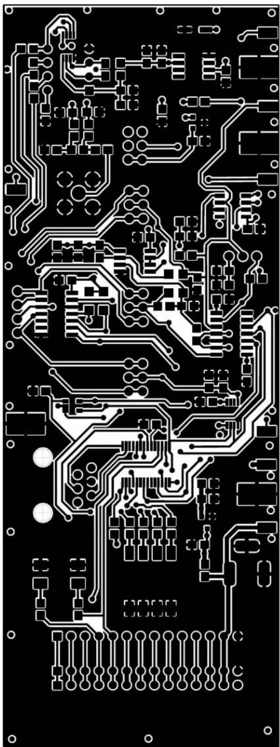
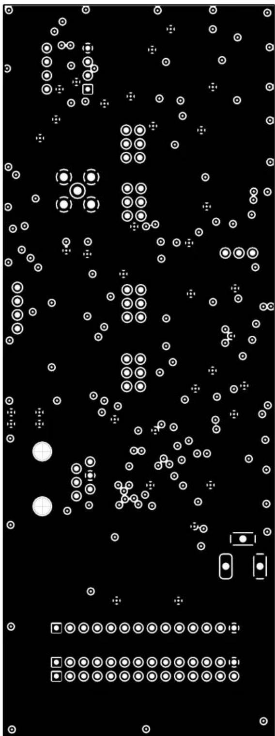
Appendix A. Schematics and Layouts
A.1 INTRODUCTION
This appendix contains the schematics and layouts for the Mixed Signal PICtail™ Demo Board.
Diagrams included in this appendix:
- Board Schematic
• Board - Top + Silk Screen Layer - Board - Power Layer
- Board - Top Layer
- Board - Bottom Layer
- Board - Ground Layer
FIGURE A-1: BOARD SCHEMATIC - PAGE 1
text_image
A B C D E F U11 U9 MCP1541 REF19BG R24 C14 0.1uF C23 1uF C15 0.01uF C22 0.8 0.8 R9 100 100 100 100 R12 1K 0.01uF/U6 1.V67 V687 R36 1K 0.01uF/U6 2.V67 R11 1K 0.01uF/U6 3.V67 R29 1K 0.01uF/U6 4.V67 C21 0.81uF C27 0.8 0.8 VDD2 +VDD2 R14 +VDD2 18K 18K +VDD2 R28 18K +VDD2 TC1321 U7 +VDD2 C28 TP3 R28 +VDD2 100pF J4 RJ1 6PIN U1 GCU/RCS RST/PDC 77.CN RCC/CC 2 RSE/RDC 77.CN RCC/CC 3 RSS/AM3/CC/PD 77.CN RCC/CC 4 RSS/AM3/VHT-/(CV/BR4/AM1) 77.CN RCC/CC 5 RSS/AM3/VHT-RCD/CC/P2/AM3 77.CN RCC/CC 6 RSS/AM3/TDDG/C/DUT RSS/AM3 77.CN RCC/CC 7 RSS/AM3/AN/A/CON/SS/RB/AN/B 77.CN RCC/CC 8 RSS/AT/AM3/UHT/A/A 77.CN RCC/CC 9 RSS/T150/T100 RC7/RV/C7 77.CN RCC/CC 10,RSS/T150/CC/P2 RC6/RV/C6 77.CN RCC/CC 11,RSS/CC/P2 RC4/SD/SD/A 77.CN RCC/CC 12,RSS/CC/P2 RC4/SD/SD/A 77.CN PIC187/N67_55DP VREF_DAC VREF_ADC • See Note 3 VREF_DAC VREF_DAC MICROCHIP Temp: J. Simane Date: Tue Nov 02, 2004 Drawn by: A.Garcia Flawnm: Mixed Signal PICtail User: Data: 524-2 A B C D E FFIGURE A-1: BOARD SCHEMATIC - CONTINUED
text_image
A B C D E F 1 2 3 4 1 2 3 4 1 2 3 4 1 2 3 4 1 2 3 4 1 2 3 4 1 2 3 4 1 2 3 4 1 2 3 4 1 2 3 4 1 2 3 4 1 2 3 4 1 2 3 4 1 3 4 1 2 3 4 1 2 3 4 1 2 3 4 1 2 3 4 1 2 3 4 1 2 3 4 1 2 3 4 1 2 3 4 1 2 3 4 1 2 3 4 1 2 3 4 1 2 3FIGURE A-2: BOARD LAYOUT - TOP + SILK-SCREEN LAYER
text_image
R17 RT6 RT5 U8N C27 9N C21 R11 R12 C17 R29 R31 R30 VREF_ADC R27 C19 R23 J7 JP3 AIN B Vout B AIN D R25 C11 U12 90 S0 C10 SHDN JP5 Vref J8 U3 C12 R20 AIN C R14 Vout A JP2 R10 C18 R21 9ZN C13 R6 AIN A R18 R19 R22 C20 0 LN R28 C5 AIN D Vout C AIN C C28 U7 C4 J4 ICD-2 +VDD2 U1 424 R1 R2 R3 R4 C2 C1 U4 J5 D2 D1 S1 L1 R8 R7 9VDC SW2 SW1 SW0 LED1 LED0 VREF LDAC CS1 SD0 SDA SCL CS0 Vin GND P1 RA5 RA4 RA3 RC5 RC4 RC3 RA0 RA1 RA2 RC0 RC1 RC2 VDD GND Mixed Signal Bd. 102-00027FIGURE A-3: BOARD LAYOUT - POWER LAYER

text_image
Circuit board layout diagram with labeled components and circular component placementsFIGURE A-4: BOARD LAYOUT - TOP LAYER
natural_image
Pure electrical circuit lines without any symbolsFIGURE A-5: BOARD LAYOUT - BOTTOM LAYER

natural_image
Pure electrical circuit lines without any symbols or text, rendered in white on a black background (no readable text or labels)FIGURE A-6: BOARD LAYOUT - GROUND LAYER
natural_image
Black-and-white abstract pattern with scattered white circles and geometric shapes (no text or symbols)Appendix B. Bill-Of-Materials (BOM)
TABLE B-1: BILL-OF-MATERIALS (BOM)
| Qty | Reference Description Manufacturer | Part Number | |||
| 1 C1 Capacitor, Ceramic, 1000 pf | 50V, 5%, C0G 0805 | Murata Electronics®North America | GRM2165C1H102JA01D | ||
| 11 C4, C5, C9, C10, C12, C13,C15, C21, C22, C27, C28 | Capacitor, 10000 pf, 50VCeramic, X7R 0805 | Kemet® | C0805C103K5RACTU | ||
| 6 C3, C8, C11, C16, C17, C24 Capacitor, .1 uf, 16VCeramic X7R 0805 | Panasonic®- ECG ECJ-2VB1C104K | ||||
| 4 C2, C14, C23, C26 Capacitor, 1 uf, 16VCeramic Y5V 0805 | Panasonic - ECG ECJ-2VF1C105Z | ||||
| 4 C6, C18, C19, C20 Capacitor, Ceramic 100 pf,50V, NP0 0805 | Kemet | C0805C101J5GACTU | |||
| 1 | C25 | Capacitor, 10 uf, 16V, SMT | Panasonic VS series | ECEV1CS100SR | |
| 1 D2 LED, Green, 565 nm, PLCC, | 120 deg | Lite-On TradingUSA, Inc. | LTST-T670GKT | ||
| 1 D1 LED, 2.8x3.2 mm, 635 nm, | Red, CLR SMD | Lumex® Opto/Components Inc. | SML-LX2832IC-TR | ||
| 2 J1, J2 | Conn, | Header, 14pos, .100Vert Tin | Molex®/Waldom®Electronics Corp. | 22-28-4140 | |
| 1 J4 | Conn, | Mod Jack, 6-6 R/A,PCB 50AU | AMP/TycoElectronics | 520470-3 | |
| 1 J5 | Conn, | Power Jack, 2.5 mm,PCB CIRC | CUI Inc | PJ-102B | |
| 1 J7 | Do Not | PopulateConnectors, RF, Jack, SMA | SPC Technology | SPC10611 | |
| 4 JP1, JP2, JP3, JP4 | Conn, | Header, 6pos, .100,Vert Gold | Molex/WaldomElectronics Corp. | 10-89-1061 | |
| 1 JP5 | Conn, | Header, 3pos, .100,Vert Tin | Molex/WaldomElectronics Corp. | 22-28-4030 | |
| 1 L1 | Inductor, Fixed, 10 uh,Type 7BA | Toko America | 144LY-100J | ||
| 1 P1 | Conn, | Header, 14pos, .100,R/A Tin | Molex/WaldomElectronics Corp. | 22-28-8140 | |
| 3 | R23, R29, R30 | Resistor, 0.0Ω, 1/8w, 5%,0805 SMD | Panasonic - ECG ERJ-6GEY0R00V | ||
| 6 | R1, R2, R3, R4, R11, R12 | Resistor, 1.00 kΩ, 1/10w, 1%0805 SMD | Panasonic - ECG ERJ-6ENF1001V | ||
| 2 | R18, R22 | Resistor, 1.00 mΩ, 1/10w, 1%0805 SMD | Panasonic - ECG ERJ-6ENF1004V | ||
| 4 | R25, R26, R27, R28 | Resistor, 4.99 kΩ ,1/10w, 1%0805 SMD | Panasonic - ECG ERJ-6ENF4991V | ||
| 2 R10, R31 | Do Not | Populate | |||
| 6 | R5, R6, R14, R20, R24 | Resistor, 10.0 kΩ, 1/10w, 1%0805 SMD | Panasonic - ECG ERJ-6ENF1002V | ||
TABLE B-1: BILL-OF-MATERIALS (BOM) (CONTINUED)
| Qty | Reference | Description | Manufacturer | Part Number |
| 5 R9, R13 | R15, R16, R17 Resistor, 1 | 00Ω, 1/10w, 1%0805 SMD | Panasonic - ECG ER | J-6ENF1000V |
| 2 R7, R8 | Resistor, 470Ω, 1/8w, 5% | 0805 SMD | Panasonic - ECG ER | J-6GEYJ471V |
| 1 R21 | Resistor, 0.0Ω, 1/4w, 5% | 1206 SMD | Yageo America 9C12 | 063A0R00JLHFT |
| 1 S1 Switch, Dip 4-pos, | Top Slide SMT | CTS Corporation Resistor/Electrocomponents | 204-4ST | |
| 12 TP1, | TP2, TP3, TP4, TP5,TP6, TP7, TP8, TP9, TP10,TP11, TP12 | PC, Test Point, MiniatureSMT | Keystone Electronics® | 5015 |
| 1 U1 Microcontroller, 8-bit, CMOS | Flash with 10-bit A/D | Microchip Technology Inc. | MCP16F767-I/SS | |
| 1 U4 Low Dropout Positive Voltage | Regulator | Microchip Technology Inc. | TC55RP5001ECB713 | |
| 1 U7 10-bit Digital-to-Analog | Converter | Microchip Technology Inc. | TC1321EUA | |
| 1 U9 Vo | tage Reference, 4.096V Microchip | Technology Inc. | MCP1541-I/TT | |
| 1 U11 IC Volt Ref, LDO, 4.096V, | 8-pin SOIC | Analog Devices Inc. | REF198GS | |
Appendix C. MixedSignal\_V100.asm Description
Software License Agreement
The software supplied herewith by Microchip Technology Incorporated (the "Company") is intended and supplied to you, the Company's customer, for use solely and exclusively with products manufactured by the Company.
The software is owned by the Company and/or its supplier, and is protected under applicable copyright laws. All rights are reserved. Any use in violation of the foregoing restrictions may subject the user to criminal sanctions under applicable laws, as well as to civil liability for the breach of the terms and conditions of this license.
THIS SOFTWARE IS PROVIDED IN AN "AS IS" CONDITION. NO WARRANTIES, WHETHER EXPRESS, IMPLIED OR STATUTORY, INCLUDING, BUT NOT LIMITED TO, IMPLIED WARRANTIES OF MERCHANTABILITY AND FITNESS FOR A PARTICULAR PURPOSE APPLY TO THIS SOFTWARE. THE COMPANY SHALL NOT, IN ANY CIRCUMSTANCES, BE LIABLE FOR SPECIAL, INCIDENTAL OR CONSEQUENTIAL DAMAGES, FOR ANY REASON WHATSOEVER.
TABLE C-1: MIXEDSIGNAL V100.ASM
TITLE "Mixed Signal PICtail(TM) Board Firmware"
;*****
; Author: Jim Simons
; Tools: MPLAB(R) IDE 6.62 using MPLINK(tm) Linker
; Editor: ComicSans 8pt w/8 character Tabs
; Files: MixedSignal_v100.asm
; DAC_dtmf.asm
; MixedSignal_16f767i.lkr
; p16f767inc
;
; Description: Use the DIP Switches to select the mode of operation. The PIC(R) MCU then
; polls for changes in the DIP switches. If a change is detected for 100ms during 500ms of
; scanning, a new mode is selected.
;
; MCP4922 DAC modes
; Mode0000: Flash LEDs and Dial a phone number stored in memory.
; Mode0001: Send 000h & FFFh commands to generate a 100Hz R-R output on the MCP4922.
; Mode0010: Send 400h & BFFh commands to generate a 100Hz output on the MCP4922.
; Mode0011: DACA = SHDN, DACB = SHDN, PIC = SLEEP
; Mode0100: DACB & DACA = 800h & Read w/PIC16F767 10b ADC, "broadcast on USART"
; Mode0101: DACB = 801h, DACA = 800h & Read w/MCP3302 13b Dif, "broadcast on USART"
; Mode0110: DACB & DACA = 800h & Read w/MCP3551, "broadcast on USART"
; Mode0111: Open for user to define their own routine.
; TC132X DAC modes (MUST DEFINE WHICH SPECIFIC DEVICE BELOW)
; Mode1000: Flash LEDs and generate a 100Hz 32step sine wave on the TC1321.
; Mode1001: Send 000h & FFFh commands to generate a 100Hz R-R output on the TC1321.
; Mode1010: Send 400h & BFFh commands to generate a 100Hz output on the TC1321.
; Mode1011: DAC = SHDN, PIC = SLEEP
; Mode1100: DAC = 200h & Read w/PIC16F767 10b ADC, "broadcast on USART"
; Mode1101: DAC = 200h & Read w/MCP3302 13b single-ended, "broadcast on USART"
; Mode1110: Open for user to define their own routine.
; Mode1111: Open for user to define their own routine.
;
Due to file size, only the first page of MixedSignal_V100.asm is shown in Table C-1. Please refer to the Microchip web site at www.microchip.com to download and view the latest version of this firmware.
NOTES:
Appendix D. DAC\_dtmf.asm Source Code
Software License Agreement
The software supplied herewith by Microchip Technology Incorporated (the "Company") is intended and supplied to you, the Company's customer, for use solely and exclusively with products manufactured by the Company.
The software is owned by the Company and/or its supplier, and is protected under applicable copyright laws. All rights are reserved. Any use in violation of the foregoing restrictions may subject the user to criminal sanctions under applicable laws, as well as to civil liability for the breach of the terms and conditions of this license.
THIS SOFTWARE IS PROVIDED IN AN "AS IS" CONDITION. NO WARRANTIES, WHETHER EXPRESS, IMPLIED OR STATUTORY, INCLUDING, BUT NOT LIMITED TO, IMPLIED WARRANTIES OF MERCHANTABILITY AND FITNESS FOR A PARTICULAR PURPOSE APPLY TO THIS SOFTWARE. THE COMPANY SHALL NOT, IN ANY CIRCUMSTANCES, BE LIABLE FOR SPECIAL, INCIDENTAL OR CONSEQUENTIAL DAMAGES, FOR ANY REASON WHATSOEVER.
TABLE D-1: DAC_DTMF.ASM
Mixed Signal PICtail™ Demo Board User's Guide
; OUTPUT - 5 cycles
;
; THEORY OF OPERATION - CHOOSING # OF STEPS
; Using the above #s:
; Minimum loop = 17 cycles
; Maximum loop = 46 cycles
; Maximum Low distortion = 5 + 22 + 5 = 32
; Maximum High distortion = 5 + 19 + 5 = 29
;
; These numbers need to be taken into consideration when choosing Fosc
; and the # of steps. Obviously, there is a balance between adding
; more steps (doesn't have to be 2^X # of steps) and the distortion
; caused by not executing the minimum loop very often. The user could
; model this with most mathematical software packages to determine
; what is best for their system.
;
;*****
DTMF    UDATA
F_Low    RES 1 ;# of cycles for the low frequency
F_Low_Rolling    RES 1 ;last value of TMR0 when F_Low_Out was updated
F_Low_Step    RES 1 ;SINE table index
F_Low_Out    RES 1 ;Output duty cycle for F_Low
F_High    RES 1 ;# of cycles for the high frequency
F_High_Rolling    RES 1 ;last value of TMR0 when F_High_Out was updated
F_High_Step    RES 1 ;SINE table index
F_High_Out    RES 1 ;Output duty cycle for F_High
DTMF_Out    RES 1 ;Output for DAC
ToneLength    RES 1 ;# of F_High cycles used for delay
Key_Value    RES 1 ;what # to dial?
GLOBAL F_Low, F_Low_Rolling, F_Low_Step, F_Low_Out, F_High, F_High_Rolling
GLOBAL F_High_Step, F_High_Out, DTMF_Out, ToneLength, Key_Value
GLOBAL Tone, Repeat_tone
EXTERN DAC_MSB, DAC_LSB, WriteToMCP492X
DTMF_SUB CODE
;
; Conditional Assembly Control Words
; ;No = 0, Yes = 1
#DEFINE Fosc_8000000 1 ;8MHz oscillator
#DEFINE Fosc_4000000 0 ;4MHz oscillator
#DEFINE Fosc_3570000 0 ;3.57MHz oscillator

#DEFINE ToneLength_150 0 ;150 ms tone per subroutine call
#DEFINE ToneLength_100 0 ;100 ms tone per subroutine call
#DEFINE ToneLength_50 1 ;50 ms tone per subroutine call

if Fosc_8000000
#DEFINE _32_steps 0 ;32 steps per cycle
#DEFINE _16_steps 1 ;16 steps per cycle
endif
if Fosc_4000000 | Fosc_3570000
#DEFINE _32_steps 0 ;32 steps per cycle
#DEFINE _16_steps 1 ;16 steps per cycle
endif

if _32_steps
;
;
; This is a 32 level lookup table of a 7 bit SINE wave
; Y = 7 bit result X = step #
;
; Y = 63 + 64 * Sin (X * 360 / 32)
;
SINE_Table_7bit ;32 step
    addwf PCL,F
    nop ;this location is never used since W != 0
    DT .63, .75, .87, .99, .108, .116, .122, .126
    DT .127, .126, .122, .116, .108, .99, .87, .75
    DT .63, .51, .39, .27, .18, .10, .4, .1
    DT .0, .1, .4, .10, .18, .27, .39, .51
    endif

; if _32_steps & _8_bit
;*****
; 32 step lookup table of an 8 bit SINE wave
;    Y = 8 bit result
;    X = step #
;    Y = 127 + 128 * Sin (X * 360 / 32)
;
; SINE_Table_32step_8bit
; addwf PCL,F
; nop ;this location is never used since W != 0
; DT .127, .152, .176, .198, .218, .233, .245, .253
; DT .255, .253, .245, .233, .218, .198, .176, .152
; DT .127, .102, .78, .56, .36, .21, .9, .1
; DT .0, .1, .9, .21, .36, .56, .78, .102
; endif

if _16_steps
;
;*****
; This is a 16 level lookup table of a 7 bit SINE wave
;    Y = 7 bit result X = step #
;
;    Y = 63 + 64 * Sin (X * 360 / 16)
;
SINE_Table_7bit ;16 step
    addwf PCL,F
    nop ;this location is never used since W != 0
DT .63, .87, .108, .122
DT .127, .122, .108, .87
DT .63, .39, .18, .4
DT .0, .4, .18, .39
endif

;*****
; DTMF Frequency Tables
;
Key Low High
0 941 1336
1 697 1209
2 697 1336
3 697 1477
4 770 1209
5 770 1336
6 770 1477
Mixed Signal PICtail™ Demo Board User's Guide
; 7 852 1209
; 8 852 1336
; 9 852 1477
; A 697 1633
; B 770 1633
; C 852 1633
; D 941 1633
; * 941 1209
; # 941 1477

if ((_32_steps) & (Fosc_8000000)) | ((_16_steps) & (Fosc_4000000))
;*****
; Delay Calculation for Frequency Generation
; Fosc = 8MHz #steps = 32
; OR
; Fosc = 4MHz #steps = 16
;
; X = Fosc / (4 * #steps * Ftone)
;
F_Low_table
addwf PCL,F
;X Actual Desired %Error
retlw .66 ;947.0 941 .63%
retlw .90 ;694.4 697 .37%
retlw .90 ;694.4 697 .37%
retlw .90 ;694.4 697 .37%
retlw .81 ;771.6 770 .21%
retlw .81 ;771.6 770 .21%
retlw .81 ;771.6 770 .21%
retlw .73 ;856.2 852 .49%
retlw .73 ;856.2 852 .49%
retlw .73 ;856.2 852 .49%
retlw .90 ;694.4 697 .37%
retlw .81 ;771.6 770 .21%
retlw .73 ;856.2 852 .49%
retlw .66 ;947.0 941 .63%
retlw .66 ;947.0 941 .63%
retlw .66 ;947.0 941 .63%

F_High_table
addwf PCL,F
;X Actual Desired %Error
retlw .47 ;1329.8 1336 .47%
retlw .52 ;1201.9 1209 .59%
retlw .47 ;1329.8 1336 .47%
retlw .42 ;1488.1 1477 .75%
retlw .52 ;1201.9 1209 .59%
retlw .47 ;1329.8 1336 .47%
retlw .42 ;1488.1 1477 .75%
retlw .38 ;1644.7 1633 .72%
retlw .38 ;1644.7 1633 .72%
retlw .38 ;1644.7 1633 .72%
retlw .52 ;1201.9 1209 .59%
retlw .42 ;1488.1 1477 .75%
endif

if _16_steps & Fosc_8000000
;
;
;
; Delay Calculation for Frequency Generation
; Fosc = 8MHz #steps = 16
;
; X = Fosc / (4 * #steps * Ftone)
;
;
F_Low_table
addwf PCL,F
;X Actual Desired %Error
retlw .133 ;939.8 941 .12%
retlw .179 ;698.3 697 .19%
retlw .179 ;698.3 697 .19%
retlw .179 ;698.3 697 .19%
retlw .162 ;771.6 770 .21%
retlw .162 ;771.6 770 .21%
retlw .162 ;771.6 770 .21%
retlw .147 ;850.3 852 .19%
retlw .147 ;850.3 852 .19%
retlw .147 ;850.3 852 .19%
retlw .179 ;698.3 697 .19%
retlw .162 ;771.6 770 .21%
retlw .147 ;850.3 852 .19%
retlw .133 ;939.8 941 .12%
retlw .133 ;939.8 941 .12%
retlw .133 ;939.8 941 .12%

F_High_table
addwf PCL,F
;X Actual Desired %Error
retlw .94 ;1329.8 1336 .47%
retlw .103 ;1213.6 1209 .37%
retlw .94 ;1329.8 1336 .47%
retlw .85 ;1470.6 1477 .43%
retlw .103 ;1213.6 1209 .37%
retlw .94 ;1329.8 1336 .47%
retlw .85 ;1470.6 1477 .43%
retlw .77 ;1623.4 1633 .59% ; may run out of tcy and be too slow
retlw .77 ;1623.4 1633 .59% ; may run out of tcy and be too slow
retlw .77 ;1623.4 1633 .59% ; may run out of tcy and be too slow
retlw .77 ;1623.4 1633 .59% ; may run out of tcy and be too slow
relw .103 ;1213.6 1209 .37%
relw .85 ;1470.6 1477 .43%

endif

if _16_steps & Fosc_3570000
;
;
;
;
;
;
;
;
;
;
Mixed Signal PICtail™ Demo Board User's Guide
; Fosc = 3.57MHz #steps = 16
;
; X = Fosc / (4 * #steps * Ftone)
;
F_Low_table
addwf PCL,F
;X Actual Desired %Error
retlw .59 ;945.5 941 .47%
retlw .80 ;697.3 697 .04%
retlw .80 ;697.3 697 .04%
retlw .80 ;697.3 697 .04%
retlw .72 ;774.7 770 .72%
retlw .72 ;774.7 770 .72%
retlw .72 ;774.7 770 .72%
retlw .65 ;858.2 852 .65%
retlw .65 ;858.2 852 .65%
retlw .65 ;858.2 852 .65%
retlw .80 ;697.3 697 .04%
retlw .72 ;774.7 770 .72%
retlw .65 ;858.2 852 .65%
retlw .59 ;945.5 941 .47%
retlw .59 ;945.5 941 .47%
retlw .59 ;945.5 941 .47%
F_High_table
addwf PCL,F
;X Actual Desired %Error
retlw .42 ;1328.1 1336 .59%
retlw .46 ;1212.6 1209 .30%
retlw .42 ;1328.1 1336 .59%
retlw .38 ;1467.9 1477 .61%
retlw .46 ;1212.6 1209 .30%
retlw .42 ;1328.1 1336 .59%
retlw .38 ;1467.9 1477 .61%
retlw .46 ;1212.6 1209 .30%
retlw .42 ;1328.1 1209 .59%
retlw .38 ;1467.9 1477 .61%
retlw .34 ;1640.6 1633 .47%
retlw .34 ;1640.6 1633 .47%
retlw .34 ;1640.6 1633 .47%
retlw .34 ;1640.6 1633 .47%
retlw .46 ;1212.6 1209 .30%
retlw .38 ;1467.9 1477 .61%
endif
;**********************************************************************
; Tone Length Calculation
; How many high cycles does it take to meet the desired timeout?
;
; ToneLength = desired_length / (1/Freq_high)
;
if (ToneLength_150)
ToneLength_table
addwf PCL,F
retlw .200
retlw .181
retlw .200
retlw .222
retlw .181
retlw .200
retlw .222
retlw .181
retlw .200
retlw .222
retlw .245
retlw .245
retlw .245
retlw .245
retlw .181
retlw .222
endif
if ToneLength_100
ToneLength_table
addwf PCL, F
retlw .134
retlw .121
retlw .134
retlw .148
retlw .121
retlw .134
retlw .148
retlw .121
retlw .133
retlw .148
retlw .163
retlw .163
retlw .163
retlw .163
retlw .121
retlw .148
endif
if ToneLength_50
ToneLength_table
addwf PCL,F
retlw .67
retlw .60
retlw .67
retlw .74
retlw .60
retlw .67
retlw .74
retlw .60
retlw .67
retlw .74
retlw .82
retlw .82
retlw .82
retlw .82
retlw .60
retlw .74
endif
;**********************************************************************
Tone ;The following Syncs the SINE wave and the Timer
;Initialize all registers for startup
movlw HIGH SINE_Table_7bit
movwf PCLATH
if _32_steps
movlw .32
endif
if _16_steps
movlw .16
endif
movwf F_Low_Step
movwf F_High_Step
movlw 01Fh
movwf F_Low_Out
movwf F_High_Out
movf TMR0,W
movwf F_Low_Rolling
movwf F_High_Rolling
movlw 0Fh
andwf Key_Value,F
movf Key_Value,W
call F_Low_table
movwf F_Low
movf Key_Value,W
call F_High_table
movwf F_High

Repeat_tone ;Call here to repeat the tone for ToneLength
;The following inits the ToneLength delay reg's
movf Key_Value,W
call ToneLength_table
movwf ToneLength

test_F_Low ;Low frequency tone loop timer
movf F_Low_Rolling,W
subwf TMR0,W ;result = time since last update
subwf F_Low,W ;Carry bit determines if enough time has elapsed
btfsc STATUS,C
goto test_F_High ;do not update the SINE wave yet
movf F_Low,W
addwf F_Low_Rolling,F ;Very Important to add to the last reference
;instead of using the actual timer value
decfsz F_Low_Step,F ;update the step count
goto no_reset_F_Low_Step
if _32_steps
movlw .32
endif
if _16_steps
movlw .16
endif
movwf F_Low_Step
no_reset_F_Low_Step
movf F_Low_Step,W
call SINE_Table_7bit ;fetch the corresponding Sin value
movwf F_Low_Out ;store result

test_F_High ;High frequency tone loop timer
movf F_High_Rolling,W
subwf TMR0,W ;result = time since last update
subwf F_High,W ;Carry bit determines if enough time has elapsed
btfsc STATUS,C
goto update_output ;do not update the SINE wave yet
movf F_High,W
addwf F_High_Rolling,F ;Very Important to add to the last reference
;instead of using the actual timer value
decfsz F_High_Step,F ;update the step count
goto no_reset_F_High_Step
if _32_steps
movlw .32
endif
if _16_steps
movlw .16
endif
movwf F_High_Step
; ToneLength timer
decfsz ToneLength,F
goto no_reset_F_High_Step
; ToneLength time expired, Exit subroutine
retlw 00h

no_reset_F_High_Step
movf F_High_Step,W
call SINE_Table_7bit ;fetch the corresponding Sin value
movwf F_High_Out ;store result

update_output ;Sum the 2 7-bit SINE outputs & refresh the D/A converter
; We can output one frequency at a time for test purposes
; w/o changing any timing! (Notice the sine wave quality)
movf F_High_Out,W ;comment this line for Low frequency Only
; addwf F_High_Out,W ;uncomment this line for High frequency Only

; movf F_Low_Out,W ;uncomment this line for Low frequency Only
addwf F_Low_Out,W ;comment this line for High frequency Only
movwf DTMF_Out
xorwf DAC_LSB,W
btfsc STATUS,Z ; nothing changed so continue looping
goto test_F_Low

; movf DTMF_Out,W ; Use this if seeking an 8b result
; movwf PORTB ; Use this if R2R on PortB
; movwf CCPR1L ; Use this if utilizing a HW PWM... shifted R for speed.
swapf DTMF_Out,W ; Use this for L shift 8b -> 12b result
movwf DAC_LSB ; should mask the 4 LSBs... if we were getting picky
iorlw b'11110000' ; Use this for 12b result , set DAC B, Vref Buffered,
; 1x Gain
movwf DAC_MSB ; Use this for 12b result, otherwise let it default to
; preload
call WriteToMCP492X ; takes 30 Tcy using HW SPI
goto test_F_Low

tone_done
end
NOTES:
Appendix E. MixedSignal\_16f767i.lkr Source Code
Software License Agreement
The software supplied herewith by Microchip Technology Incorporated (the "Company") is intended and supplied to you, the Company's customer, for use solely and exclusively with products manufactured by the Company.
The software is owned by the Company and/or its supplier, and is protected under applicable copyright laws. All rights are reserved. Any use in violation of the foregoing restrictions may subject the user to criminal sanctions under applicable laws, as well as to civil liability for the breach of the terms and conditions of this license.
THIS SOFTWARE IS PROVIDED IN AN "AS IS" CONDITION. NO WARRANTIES, WHETHER EXPRESS, IMPLIED OR STATUTORY, INCLUDING, BUT NOT LIMITED TO, IMPLIED WARRANTIES OF MERCHANTABILITY AND FITNESS FOR A PARTICULAR PURPOSE APPLY TO THIS SOFTWARE. THE COMPANY SHALL NOT, IN ANY CIRCUMSTANCES, BE LIABLE FOR SPECIAL, INCIDENTAL OR CONSEQUENTIAL DAMAGES, FOR ANY REASON WHATSOEVER.
TABLE E-1: MIXEDSIGNAL_16F767I.LKR
// Sample ICD2 linker command file for 16F767 LIBPATH.
| CODEPAGE | NAME=vectors | START=0x0 | END=0x3 | PROTECTED |
| CODEPAGE | NAME=interrupt | START=0x4 | END=0x0FF | |
| CODEPAGE | NAME=page0_1 | START=0x100 | END=0x1FF | |
| CODEPAGE | NAME=page0_2a | START=0x200 | END=0x22F | |
| CODEPAGE | NAME=page0_2b | START=0x230 | END=0x2FF | |
| CODEPAGE | NAME=page0_3 | START=0x300 | END=0x3FF | |
| CODEPAGE | NAME=page0_4 | START=0x400 | END=0x4FF | |
| CODEPAGE | NAME=page0_5 | START=0x500 | END=0x5FF | |
| CODEPAGE | NAME=page0_6_7 | START=0x600 | END=0x7FF | |
| CODEPAGE | NAME=page1 | START=0x800 | END=0xFFFF | |
| CODEPAGE | NAME=page2 | START=0x1000 | END=0x17FF | |
| CODEPAGE | NAME=page3 | START=0x1800 | END=0x1EFF | |
| CODEPAGE | NAME=dbug | START=0x1F00 | END=0x1FFF | PROTECTED |
| CODEPAGE | NAME=.idlocs | START=0x2000 | END=0x2003 | PROTECTED |
| CODEPAGE | NAME=.test_vect | START=0x2004 | END=0x2005 | PROTECTED |
| CODEPAGE | NAME=.device_id | START=0x2006 | END=0x2006 | PROTECTED |
| CODEPAGE | NAME=.config | START=0x2007 | END=0x2009 | PROTECTED |
| CODEPAGE | NAME=.test | START=0x200A | END=0x203F | PROTECTED |
| DATABANK | NAME=sfr0 | START=0x0 | END=0x1F | PROTECTED |
| DATABANK | NAME=sfr1 | START=0x80 | END=0x9F | PROTECTED |
| DATABANK | NAME=sfr2 | START=0x100 | END=0x10F | PROTECTED |
| DATABANK | NAME=sfr3 | START=0x180 | END=0x18F | PROTECTED |
| DATABANK | NAME=gpr0 | START=0x20 | END=0x5F | |
| DATABANK | NAME=DTMF | START=0x60 | END=0x6F | |
| DATABANK | NAME=gpr1 | START=0xA0 | END=0xEF | |
| DATABANK | NAME=gpr2 | START=0x110 | END=0x164 | |
| DATABANK | NAME=dbgspr2 | START=0x165 | END=0x16F | PROTECTED |
| DATABANK | NAME=gpr3 | START=0x190 | END=0x1EF | |
| SHAREBANK | NAME=dbgspr | START=0x70 | END=0x70 | PROTECTED |
| SHAREBANK | NAME=dbgspr | START=0xF0 | END=0xF0 | PROTECTED |
| SHAREBANK | NAME=dbgspr | START=0x170 | END=0x170 | PROTECTED |
| SHAREBANK | NAME=dbgspr | START=0x1F0 | END=0x1F0 | PROTECTED |
| SHAREBANK | NAME=gprs | START=0x71 | END=0x7F |
| SHAREBANK | NAME=gprs | START=0xF1 | END=0xFF |
| SHAREBANK | NAME=gprs | START=0x171 | END=0x17F |
| SHAREBANK | NAME=gprs | START=0x1F1 | END=0x1FF |
| SECTION | NAME=RESET | ROM=vectors | // Reset vectors |
| SECTION | NAME=INTERRUPT | ROM=interrupt | // ROM code space -interrupt |
| SECTION | NAME=MAIN | ROM=page0_1 | // ROM code space |
| SECTION | NAME=MODE0000 | ROM=page0_2a | // ROM code space |
| SECTION | NAME=DTMF_SUB | ROM=page0_2b | // ROM code space |
| SECTION | NAME=MODE0001 | ROM=page0_3 | // ROM code space |
| SECTION | NAME=MODE1000 | ROM=page0_4 | // ROM code space |
| SECTION | NAME=OPEN | ROM=page0_5 | // ROM code space |
| SECTION | NAME=SUBROUTINES | ROM=page0_6_7 | // ROM code space |
| SECTION | NAME=PROG1 | ROM=page1 | // ROM code space |
| SECTION | NAME=PROG2 | ROM=page2 | // ROM code space |
| SECTION | NAME=PROG3 | ROM=page3 | // ROM code space |
| SECTION | NAME=IDLOCS | ROM=.idlocs | // ID locations |
| SECTION | NAME=TEST_VECT | ROM=.test_vect | // Test vector |
| SECTION | NAME=DEVICEID | ROM=.device_id | // Device ID |
| SECTION | NAME=CONFIG | ROM=.config | // Configuration bits location |
| SECTION | NAME=TEST | ROM=.test | // Test |
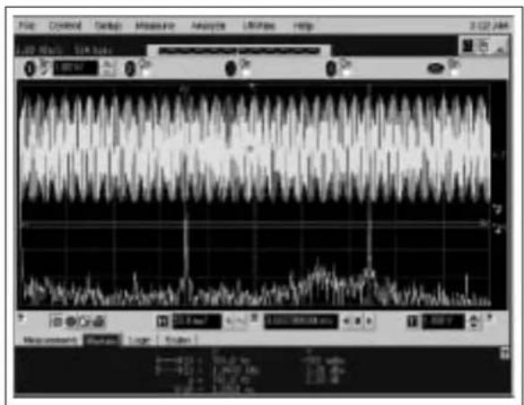
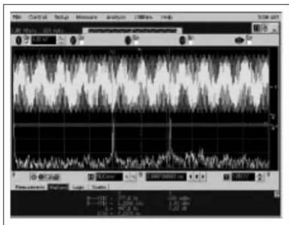
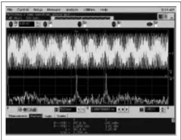
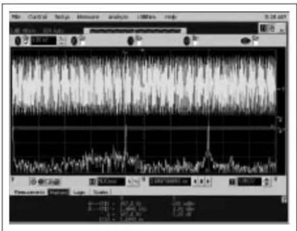
Appendix F. DTMF Scope Captures
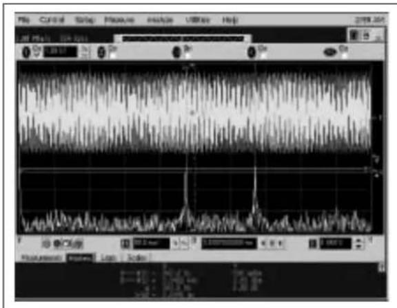
text_image
File Control Tools Feature Help Window Help OFF PA10 200 MHz Control Slope Waveform Audio VBR Help 200 MHz Signal Circuit Parameters Logic AudioFIGURE F-1: DTMF Tone 0 (941 Hz, 1336 Hz).

text_image
File Control Default Measurements Analyzer Utilities Help 2.00 AM 1.00 MHz 10A/Hz Signal Measurement Logic Scale 100000000000000000000000000000000000000000000000000000000000000000000000000000000000000 1.5678439 1.5678439 1.5678439 1.5678439 1.5678439 1.5678439 1.5678439 1.5678439 1.5678439 1.5678439 1.5678438 1.5678438 1.5678438 1.5678438 1.5678438 1.5678438 1.5678438 1.5678438 1.5678438 1.5678438 1.5678437 1.5678437 1.5678437 1.5678437 1.5678437 1.5678437 1.5678437 1.5678437 1.5678437 1.5678437 1.5678436 1.5678436 1.5678436 1.5678436 1.5678436 1.5678436 1.5678436 1.5678436 1.5678436 1.5678435 1.5678435 1.5678435 1.5678435 1.5678435 1.5678435 1.5678435 1.5678435 1.5678435 1.5678434 1.5678434 1.5678434 1.5678434 1.5678434 1.5678434 1.5678434 1.5678434 1.5678433 1.5678433 1.5678433 1.5678433 1.5678432 1.5678432 1.5678432 1.5678432 1.5678432 1.5678432 1.5678432 1.5678432 1.5678432 1.5678432 1.5678431 1.5678431 1.5678431 1.5678431 1.5678431 1.5678431 1.5678431 1.5678431 1.5678431 1.5678431 1.5678430 1.5678430 1.5678430 1.5678430 1.5678430 1.5678429 1.5678429 1.5678429 1.5678429 1.5678429 1.5678429 1.5678429 1.5678429 1.5678429 1.5678429 1.5678428 1.5678428 1.5678428 1.5678428 1.5678428 1.5678428 1.5678428 1.5678428 1.5678428 1.5678428 1.5678427 1.5678427 1.5678427 1.5678427 1.5678427 1.5678427 1.5678427 1.5678427 1.5678427 1.5678426 1.5678426 1.5678426 1.5678426 1.5678426 1.5678426 1.5678426 1.5678425 1.5678425 1.5678425 1.5678425 1.5678425 1.5678424 1.5678424 1.5678424 1.5678423 1.5678423 1.5678423 1.5678422 1.5678422 1.5678422 1.5678422FIGURE F-2: DTMF Tone 1 (697 Hz, 1209 Hz).
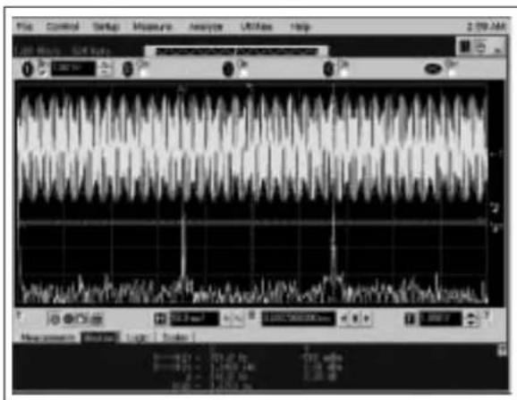
FIGURE F-3: DTMF Tone 2 (697 Hz, 1336 Hz).
text_image
File Edit Control Settings Measure Analysis Analysis Litter Help 1.20 MHz 51K Hz Measurement Settings Log: Values 1.0000000000 ns 1.0000000000 ns 1.0000000000 ns 1.0000000000 ns 1.0000000000 ns 1.0000000000 ns 1.0000000000 ns 1.0000000000 ns Control Audio SignalFIGURE F-4: DTMF Tone 3 (697 Hz, 1477 Hz).
text_image
Screenshot of a medical or electronic waveform analysis software interface showing multiple synchronized signals and time markers.FIGURE F-5: DTMF Tone 4 (770 Hz, 1209 Hz).
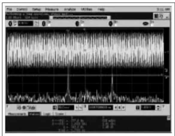
text_image
File Control Settings Pressure Analyzer Utilities Help 3:11 AM Amplitude in low-frequency, 500x 2.5V Signal: 500 MHz Signal: 500 MHz Signal: 500 MHz Signal: 500 MHz Signal: 500 MHz Signal: 500 MHz Signal: 500 MHz Signal: 500 MHz Signal: 500 MHz Signal: 500 MHz Signal: 500 MHz Signal: 500 MHz Signal: 500 MHz Signal: Signal: Log Scale Measurement Status Logic Scale S = -1.768 ± 0.01 S = -1.768 ± 0.01 S = -1.768 ± 0.01 S = -1.768 ± 0.01 S = -1.768 ± 0.01 S = -1.768 ± 0.01 S = -1.768 ± 0.01 S = -1.768 + 0.01 S = -1.768 + 0.01 S = -1.768 + 0.01 S = -1.768 + 0.01 S = -1.768 + 0.01 S = -1.768 + 0.01 S = -1.768 + 0.01 S = -2.496 ± 0.01 S = -2.496 ± 0.01 S = -2.496 ± 0.01 S = -2.496 ± 0.01 S = -2.496 ± 0.01 S = -2.496 ± 0.01 S = -2.496 ± 0.01 S = -3.232 ± 0.01 S = -3.232 ± 0.01 S = -3.232 ± 0.01 S = -3.232 ± 0.01 S = -3.232 ± 0.01 S = -3.232 ± 0.01 S = -3.232 ± 0.01 S = 2.496 ± 0.01 S = 2.496 ± 0.01 S = 2.496 ± 0.01 S = 2.496 ± 0.01 S = 2.496 ± 0.01 S = 2.496 ± 0.01 S = 2.496 ± 0.01 S = -2.496 ± 0.01 S = -2.496 ± 0.01 S = -2.496 ± 0.01 S = -2.496 ± 0.01 S = -2.496 ± 0.01 S = -2.496 ± 0.35 S = -2.496 ± 0.35 S = -2.496 ± 0.35 S = -2.496 ± 0.35 S = -2.496 ± 0.35 S = -2.496 ± 0.35 S = -2.496 ± 0.35 S = -2.496± 0. S = -2.496± 0. S = -2.496± 0. S = -2.496± 0. S = -2.496± 0. S = -2.496± 0. S = -2.496± 0. S = -2.496± 0. S = -2.496± 0. S = -3.232± 0. S = -3.232± 0. S = -3.232± 0. S = -3.232± 0. S = -3.232± 0. S = -3.232± 0. S = -3.232± 0. S = -3.232± 0. S = -3.232± 0.FIGURE F-6: DTMF Tone 5 (770 Hz, 1336 Hz).

text_image
Control Balance Measure analysis Litterbox help 10:22 AM K-100 MHz 10:22 AM 10:22 AM 10:22 AM 10:22 AM 10:22 AM 10:22 AM 10:22 AM 10:22 AM 10:22 AM 10:22 AM 10:22 AM 10:22 AM 10:22 AM 10:22 AM 10:22 AM 5.6 MHz 100 MHz 100 MHz 100 MHz 100 MHz 100 MHz 100 MHz 100 MHz 100 MHz 100 MHz 100 MHz 100 MHz 100 MHz 100 MHz 100 MHz 100 MHz 100 MHz 100 MHz 100 MHz 100 MHz 100 MHz 10.6 MHz 1.4 GHz 1.4 GHz 1.4 GHz 1.4 GHz 1.4 GHz 1.4 GHz 1.4 GHz 1.4 GHz 1.4 GHz 1.4 GHz 1.4 GHz 1.4 GHz 1.4 GHz 1.4 GHz 1.4 GHz 1.4 GHz 1.4 GHz 1.4 GHz 1.4 GHz 1.4 GHz 1.4GHzFIGURE F-7: DTMF Tone 6 (770 Hz, 1477 Hz).
text_image
Control Setup Measure analyt LDSers Help Performance of the system: A small amplitude signal in the system is measured by the DAW. The chart shows a waveform graph with a sharp peak at approximately 0.7 Hz and a gradual decline toward 0.74 Hz, indicating a transient signal event or impulse response.FIGURE F-8: DTMF Tone 7 (852 Hz, 1209 Hz).

text_image
Screenshot of a medical or scientific instrument interface displaying waveform graphs and control panel with labeled controls.FIGURE F-9: DTMF Tone 8 (852 Hz, 1336 Hz).
text_image
Screenshot of a medical or scientific analysis software interface displaying waveform graphs and control panel.FIGURE F-10: DTMF Tone 9 (852 Hz, 1477 Hz).
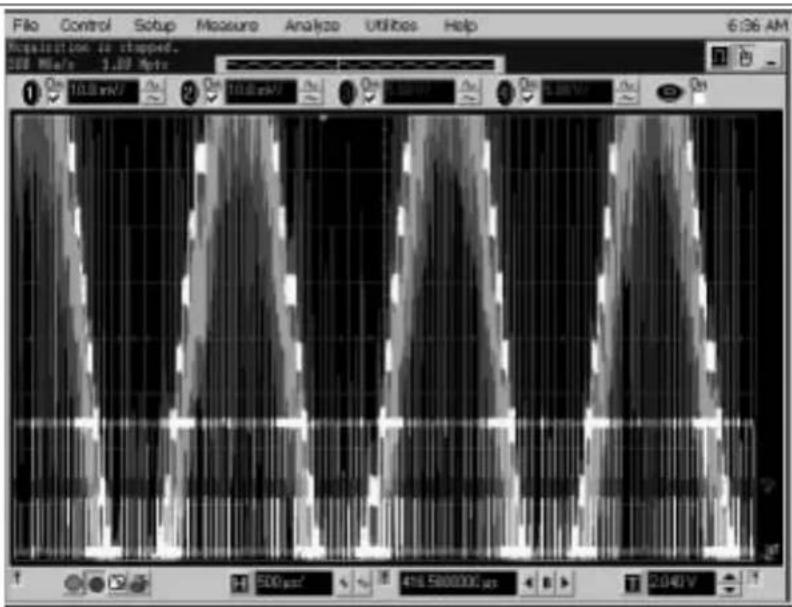
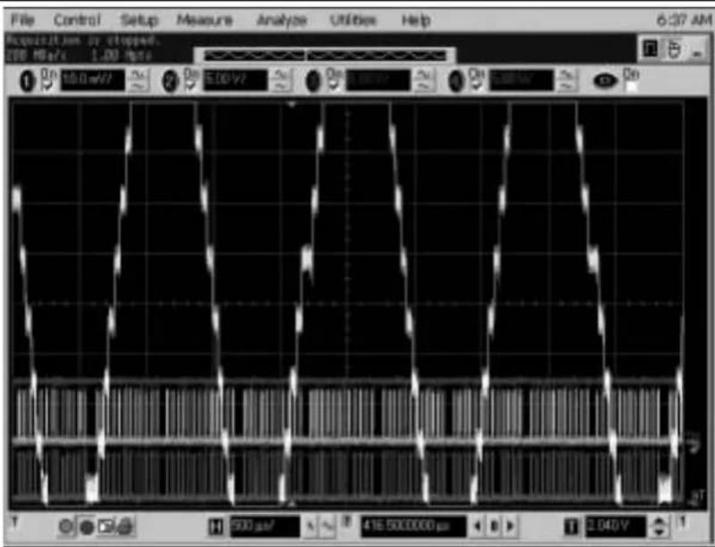
Appendix G. Scope Probe Noise Captures
text_image
File Control Setup Measure Analyze Utilities Help 6:36 AM Acquisition is stopped. 100 MHz 3.00 MHz 1 On 10.0 mV/ On 2 On 10.0 mV/ On 3 On 5.00 mV/ On 4 On 8.00 mV/ On 9 On T 500 µm² 416 5000000 ns 2.040 VFIGURE G-1: Oscilloscope screen capture of V OUT_B using a standard scope probe and short ground lead. This illustrates the noise picked up by the scope probe and ground lead.
text_image
File Control Setup Measure Analyze Utilities Help Acquisition by stopped. 100 MHz/1 1.00 MHz 6:37 AM On 100 mV? On 500 V? On 200 V? On 100 V? On 500 V? On 200 V? On 100 V? On 500 V? On 200 V? On 100 V? On 500 V? On 200 V? On 100 V? On 500 V? On 200 V? On 100 V? On 500 V? On 200 V? Up to 500 µF 416 5000000 µF 2.040 VFIGURE G-2: Oscilloscope screen capture of V OUT_D using the SMA connector and coaxial cable directly to the scope. This is the same as Figure G-1, except the scope probe on V OUT_B is turned off. This highlights how critical test connections are to properly evaluating the "real" noise in a system.
NOTES:
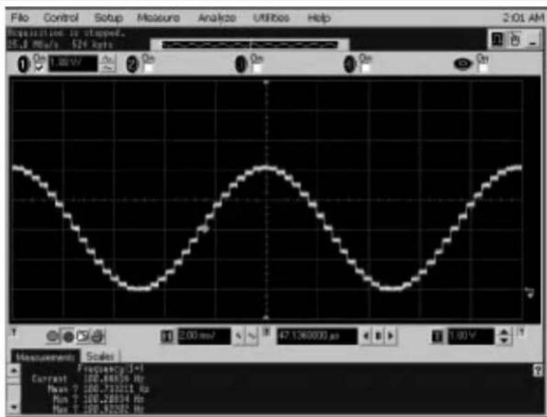
Appendix H. Sine Wave and Filtered DTMF Scope Captures
text_image
File Control Setup Measure Analyze Utilities Help Acquisition is stopped. 15.0 MHz/s 524 MHz On: 1.00 W On On On Measurement: Scales Frequency: [=1] Current: 100,68836 Hz Max: 100,717211 Hz Min: 100,76934 Hz Max: 100,83282 Hz 2:00 ms/ % 47.1360000 μs 1:00 VFIGURE H-1: Mode1000b generates a 100 Hz, 32-step sine wave on V OUT C using the TC132X.
text_image
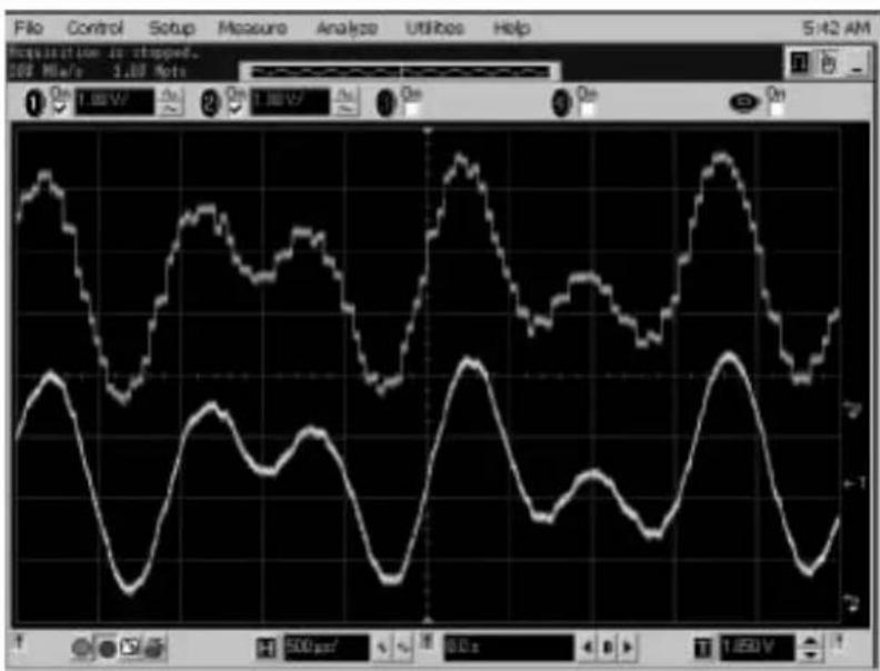
File Control Setup Measure Analyze Utilities Help 5:42 AM Acquisition is stopped. 109 MHz/s 1.00 Mpa On 1.00 V On 1.00 V On On 500 μs 0.0 s 1.050 VFIGURE H-2: Mode0000b generates DTMF waveforms to repeatedly dial a phone number. V_OUT_B illustrates the MCP4922's unfiltered output while V_OUT_D illustrates a simple low-pass filter's ability to "clean" up the signal.
NOTES:
Appendix I. MPLAB ^® IDE Screen Capture
text_image
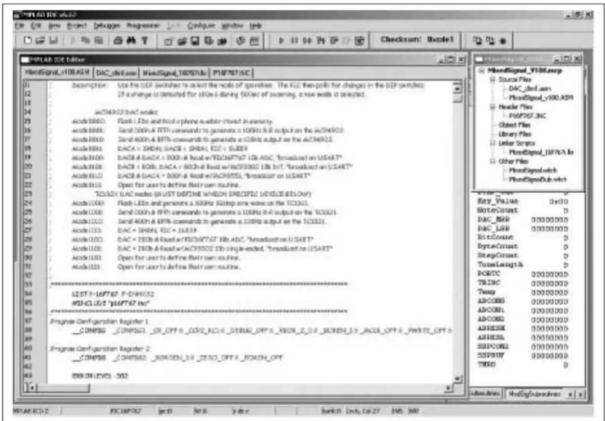
MPLAB IDE File Edit View Insert Debugging Progression Link Configure Window Help Checksum: Bxcode1 MPLAB IDE Editor HandSignal_100/ASM DAc_dac.com NewSignal_100/ASM P10P767/INC Description: Use the DSP Switches to select the node of operation. The FLC then pulls for changes in the DSP switches If a change is deleted for 100Hz during 500Hz of scanning, a new node is deleted. AC249022 DAC node ACode 8800: Flash LFEs and Hidc phone number removed in memory ACode 8801: Send 000h A RFP commands to generate x 100Hz R-R output on the AC249022 ACode 8810: Send 400h & RFP commands to generate x 100Hz output on the AC249023 ACode 8811: DAC = 2NDAL DAC = SHBN, FLC < SLIBF ACode 8100: DAC = DAC = 800h & Read w/RC249767 1Gb ADC, "broadcast on USAT" ACode 8101: DAC = 800h & Read w/RC249302 1Gb bit, "broadcast on USAT" ACode 8110: DAC = DAC = 800h & Read w/RC249351, "broadcast on USAT" ACode 8111: Open for user to define their own routine. TCI32X DAC node (ALUST BEFORE WHICH SPECIFIC SERVICE$BLOW) ACode 1000: Flash LFEs and generate x 100Hz 80Stop area write on the TC1301 ACode 1001: Send 000h & RFP commands to generate x 100Hz R-R output on the TC3321 ACode 1010: Send 400h & RFP commands to generate x 100Hz output on the TC3321 ACode 1101: DAC = SHBN, FLC < SLIBF ACode 1102: DAC = 2NDAL Read w/RC249767 1Gb ADC, "broadcast on USAT" ACode 1103: DAC = 2NDAL Read w/RC249302 1Gb single-ended, "broadcast on USAT" ACode 1104: Open for user to define their own routine. ACode 1105: Open for user to define their own routine. LIST P=16PT67 P=DH532 MDCLUD *p16PT67 Inc* Program Configuration Register 1 __COMPDS__COMPDS__OF_OFF&__COMPDS__CPU#_DUBG_OFF&_VIEUR_2_UB_SCREEN_3_D_ACEL_OFF&_PNRTE_OFF& Program Configuration Register 2 __COMPDS__COMPDS__BORDERLA_DESO_OFF&_PONCH_OFF ERR DR LEVELS -302 MeanSignal_VIRLZzmp Source Plan DAC_dacn_oam PhoDipul_v380.ASM Header Plan PdP767.INC Object Plan Library Plan Letter Script PhoDipul_LIF/FA.br Other Files PhoDipulwitch PhoDipulSub.wtch Key Value: 3x10 NoteCount: D DAC_### 00000000 DAC_L## 00000000 BitCount: D ByteCount: D StrayCount: D TotalLength: D PORTC 00000000 TRINC 00000000 Temp 00000000 ADC##D 00000000 ADC#L 00000000 ADC#D2 00000000 ADDRESS 00000000 ADDRESSL 00000000 SUPCON2 00000000 SSIPRTF 00000009 TMRD DFIGURE I-1: MPLAB ^® IDE v6.62 screen capture of an example project to build and debug the included firmware. Note the required files in the project window and the two pre-defined Watch windows that the user can open up.
WORLDWIDE SALES AND SERVICE
AMERICAS
Corporate Office
2355 West Chandler Blvd.
Chandler, AZ 85224-6199
Tel: 480-792-7200
Fax: 480-792-7277
Technical Support:
http://support.microchip.com
Web Address:
www.microchip.com
Atlanta
Alpharetta, GA
Tel: 770-640-0034
Fax: 770-640-0307
Boston
Westford, MA
Tel: 978-692-3848
Fax: 978-692-3821
Chicago
Itasca, IL
Tel: 630-285-0071
Fax: 630-285-0075
Dallas
Addison, TX
Tel: 972-818-7423
Fax: 972-818-2924
Detroit
Farmington Hills, MI
Tel: 248-538-2250
Fax: 248-538-2260
Kokomo
Kokomo, IN
Tel: 765-864-8360
Fax: 765-864-8387
Los Angeles
Mission Viejo, CA
Tel: 949-462-9523
Fax: 949-462-9608
San Jose
Mountain View, CA
Tel: 650-215-1444
Fax: 650-961-0286
Toronto
Mississauga, Ontario,
Canada
Tel: 905-673-0699
Fax: 905-673-6509
ASIA/PACIFIC
Australia - Sydney
Tel: 61-2-9868-6733
Fax: 61-2-9868-6755
China - Beijing
Tel: 86-10-8528-2100
Fax: 86-10-8528-2104
China - Chengdu
Tel: 86-28-8676-6200
Fax: 86-28-8676-6599
China - Fuzhou
Tel: 86-591-8750-3506
Fax: 86-591-8750-3521
China - Hong Kong SAR
Tel: 852-2401-1200
Fax: 852-2401-3431
China - Shanghai
Tel: 86-21-5407-5533
Fax: 86-21-5407-5066
China - Shenyang
Tel: 86-24-2334-2829
Fax: 86-24-2334-2393
China - Shenzhen
Tel: 86-755-8203-2660
Fax: 86-755-8203-1760
China - Shunde
Tel: 86-757-2839-5507
Fax: 86-757-2839-5571
China - Qingdao
Tel: 86-532-502-7355
Fax: 86-532-502-7205
ASIA/PACIFIC
India - Bangalore
Tel: 91-80-2229-0061
Fax: 91-80-2229-0062
India - New Delhi
Tel: 91-11-5160-8631
Fax: 91-11-5160-8632
Japan - Kanagawa
Tel: 81-45-471-6166
Fax: 81-45-471-6122
Korea - Seoul
Tel: 82-2-554-7200
Fax: 82-2-558-5932 or
82-2-558-5934
Singapore
Tel: 65-6334-8870
Fax: 65-6334-8850
Taiwan - Kaohsiung
Tel: 886-7-536-4818
Fax: 886-7-536-4803
Taiwan - Taipei
Tel: 886-2-2500-6610
Fax: 886-2-2508-0102
Taiwan - Hsinchu
Tel: 886-3-572-9526
Fax: 886-3-572-6459
EUROPE
Austria - Weis
Tel: 43-7242-2244-399
Fax: 43-7242-2244-393
Denmark - Ballerup
Tel: 45-4450-2828
Fax: 45-4485-2829
France - Massy
Tel: 33-1-69-53-63-20
Fax: 33-1-69-30-90-79
Germany - Ismaning
Tel: 49-89-627-144-0
Fax: 49-89-627-144-44
Italy - Milan
Tel: 39-0331-742611
Fax: 39-0331-466781
Netherlands - Drunen
Tel: 31-416-690399
Fax: 31-416-690340
England - Berkshire
Tel: 44-118-921-5869
Fax: 44-118-921-5820