ATSAMA5D44 - Kit d'évaluation Microchip - Free user manual and instructions
Find the device manual for free ATSAMA5D44 Microchip in PDF.

User questions about ATSAMA5D44 Microchip
0 question about this device. Answer the ones you know or ask your own.
Ask a new question about this device
Download the instructions for your Kit d'évaluation in PDF format for free! Find your manual ATSAMA5D44 - Microchip and take your electronic device back in hand. On this page are published all the documents necessary for the use of your device. ATSAMA5D44 by Microchip.
USER MANUAL ATSAMA5D44 Microchip
natural_image
Close-up of a blue printed circuit board (PCB) with various electronic components and connectors, no visible text or symbols.Introduction
This user guide introduces the Atmel® SAMA5D4 Xplained Ultra evaluation kit (SAMA5D4-XULT) and describes the development and debugging capabilities for applications running on the Atmel | SMART SAMA5D4 ARM® Cortex®-A5-based embedded microprocessor unit (eMPU).
Scope
This guide provides details on the SAMA5D4-XULT. It is made up of four main sections:
• Section 1. describes the evaluation kit content and its main features.
• Section 2. provides instructions to power up the SAMA5D4-XULT board.
• Section 3. provides an overview of the SAMA5D4-XULT board.
• Section 4. describes the SAMA5D4-XULT board components.
Kit Contents
The SAMA5D4-XULT includes:
- Board
— One SAMA5D4-XULT board
Cables
— One Micro-AB type USB cable - Welcome letter
Table of Contents
Introduction....1
Scope 1
Kit Contents....2
Table of Contents 3
- Evaluation Kit Specifications 4
1.1 Electrostatic Warning 4
1.2 Power Supply Warning 4
- Power Source 5
2.1 Power up the Board....5
2.2 Sample Code and Technical Support 5
- Hardware Overview 6
3.1 Introduction....6
3.2 Equipment List....6
3.3 Board Features 6
- Board Components ..... 7
4.1 Board Overview....7
4.2 Function Blocks....9
4.3 PIO Usage and Interface Connectors 41
4.4 SAMA5D4-XULT Board Schematics....57
- Revision History 72
1. Evaluation Kit Specifications
Table 1-1. Evaluation Kit Specifications
| Characteristic Specifications | ||
| Board SAMA5D4-XULT | ||
| Board supply voltage | USB powered5VDC from optional jack connector or from “Arduino shield” | |
| Temperature | Operating 0°C to | +70°C |
| Storage -40°C to | +85°C | |
| Relative Humidity 0 to 90% (non-condensing) | ||
| Dimensions: Main board 135 × 88 × 20 mm | ||
| RoHS status Compliant | ||
| Board Identification SAMA5D4-XULT | ||
1.1 Electrostatic Warning

WARNING

Electrostatic sensitive device
ESD-Sensitive Electronic Equipment!
The evaluation kit is shipped in a protective anti-static package. The board system must not be subject to high electrostatic potentials.
We strongly recommend using a grounding strap or similar ESD protective device when handling the board in hostile ESD environments (offices with synthetic carpet, for example). Avoid touching the component pins or any other metallic element on the board.
1.2 Power Supply Warning

WARNING
Hardware Power Supply Limitation
Using a power adapter greater than 5Vcc (e.g., the 12Vcc power adapters from other kits such as Arduino kits) may damage the board.

WARNING
Hardware Power Budget
Using the USB as the main power source (max. 500 mA) is acceptable only with the use of the on-board peripherals and low-power LCD extension.
When external peripheral or add-on boards need to be powered, we recommend the use of an external power adapter connected to the J4 DC jack (can provide up to 1.2A on the 3.3V node).
2. Power Source
Several options are available to power up the SAMA5D4-XULT board.
The board can be:
- USB-powered through the USB Micro-AB connector (J11 - default configuration).
- Powered through an external AC-to-DC adapter connected via a 2.1 mm center-positive plug into the optional power jack of the board (J4). The recommended output voltage range of the power adapter is 5V at 2A.
- Powered through the Arduino shield.
- Powered through the USB Micro-AB connector on the Atmel Embedded Debugger (EDBG) interface (J20).

WARNING
Unlike Arduino Uno boards, the SAMA5D4-XULT board runs at 3.3V. The maximum voltage that the I/O pins can tolerate is 3.3V. Providing higher voltages (e.g., 5V) to an I/O pin could damage the board.
2.1 Power up the Board
Unpack the board, taking care to avoid electrostatic discharge. Connect the USB Micro-AB cable to the connector (J11). Then connect the other end of the cable to a free USB port of your PC.
Table 2-1. Electrical Characteristics
| Electrical Parameter Values | |
| Input voltage 5 VCC | |
| Maximum Input voltage (limits) 6 VCC | |
| Max DC 3v3 current available 1.2A | |
| I/O Voltage 3.3V only |
2.2 Sample Code and Technical Support
After boot up, you can run some sample code or your own application on the development kit. You can download sample code and get technical support from the Atmel website.
Linux software and demos can be found on the website Linux4SAM.
3. Hardware Overview
3.1 Introduction
The Atmel SAMA5D4-XULT is a fully-featured evaluation platform for the Atmel SAMA5D4 series ARM-based embedded microprocessor units (eMPU). It allows users to extensively evaluate, prototype and create application-specific designs.
3.2 Equipment List
The SAMA5D4-XULT board is based on the integration of an ARM Cortex-A5-based microprocessor with external memory, one Ethernet physical layer transceiver, two SD/MMC interfaces, two host USB ports and one device USB port, one 24-bit RGB LCD and HDMI interface and debug interfaces.
Seven headers, compatible with Arduino R3 (Uno, Due) and two Xplained headers are available for various shield connections.
3.3 Board Features
Table 3-1. Board Specifications
| Characteristics Specifications | |
| Dimensions (L x W x H) | 135 × 88 × 20 mm |
| Processor SAMA5D44 (361-ball BGA package), 16x16 mm body, pitch 0.8 mm | |
| Oscillators | MPU, EDBG: 12 MHz quartzRTC: 32.768 kHzPHY: 25 MHz |
| Main Memory | 2 x DDR2 2 Gb 16 Meg x 16 x 8 banks (total 4 Gbit = 512 MB)1 x SLC NAND Flash 4 Gb 8-bit data (total 4 Gbit = 512 MB) |
| Accessory memories | One optional Serial EEPROM SPIOne EEPROM with Mac Address and Serial Number |
| SD/MMC | One 4-bit SD card connectorOne 4-bit Micro-SD card connector |
| USB | Two USB Hosts with power switchOne Micro-AB USB device |
| Display | One LCD interface connector, LCD TFT Controller with overlay, alpha-blending, rotation, scaling and color space conversion |
| One HDMI interface and connector | |
| Ethernet One Ethernet PHY (RMII 10/100MHz) | |
| Debug port | One JTAG interface connectorOne EDBG interfaceOne serial DBGU interface (3v3 level) |
| Expansion connector | Arduino R3 compatible set of connectorsXPRO set of connectors |
| Board supply voltage | 5V from USB, power jack, and Arduino shieldOn-board power regulation by PMIC |
| Battery On-board battery socket | |
| User interface | Reset, Wake-up and free user push buttonOne red user/power LEDOne blue user LED |
4. Board Components
4.1 Board Overview
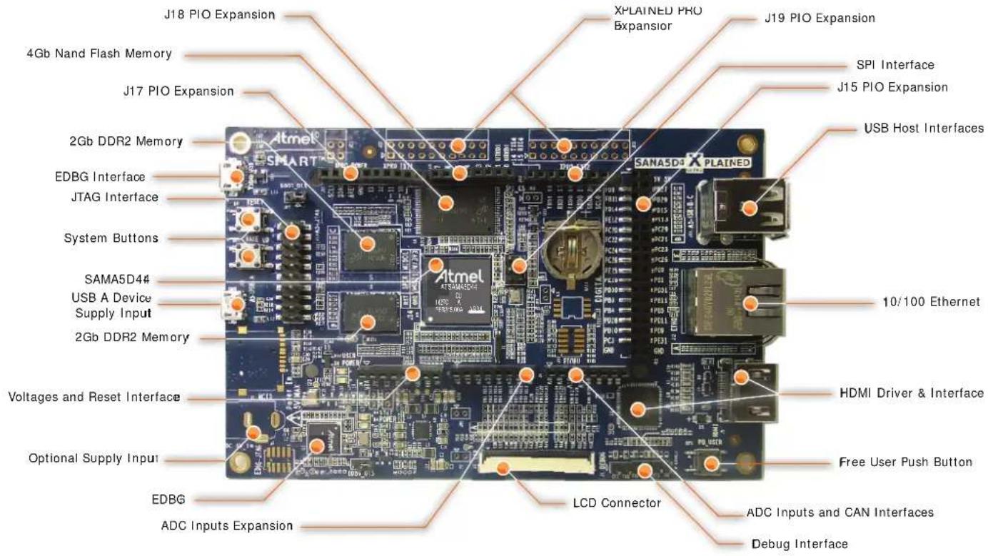
The fully-featured SAMA5D4-XULT board integrates multiple peripherals and interface connectors, as shown in Figure 4-1.
Figure 4-1. SAMA5D4-XULT Board Overview
text_image
J18 PIO Expansion 4Gb Nand Flash Memory J17 PIO Expansion 2Gb DDR2 Memory EDBG Interface JTAG Interface System Buttons SAMA5D4# USB A Device Supply Input 2Gb DDR2 Memory Voltages and Reset Interface Optional Supply Input EDBG ADC Inputs Expansion LCD Connector XPLAINED PRO Expansion J19 PIO Expansion SPI Interface J15 PIO Expansion USB Host Interfaces Atmel SANA5D4 XPLAINED 10/100 Ethernet HDMI Driver & Interface Free User Push Button ADC Inputs and CAN Interfaces Debug InterfaceTable 4-1 describes the interface connectors on the SAMA5D4-XULT.
Table 4-1. SAMA5D4-XULT Board Interface Connectors
| Connector Interfaces to | |
| J4 Main power supply | |
| J11 USB A Device. Supports USB device using a type Micro-AB connector | |
| J16 USB Host B and C. Supports USB host using a stacked type A connector | |
| J1 Serial DBGU (3.3V level) | |
| J13 JTAG, 20 pin IDC connector | |
| J20 EDBG USB connector | |
| J9 Micro-SD connector | |
| J24 SD/MMC connector | |
| J12 Ethernet ETH0 | |
| J2 | Expansion connector with all LCD controller signals for display module connection (QTouch®, TFT LCD display with touchscreen and backlight) |
| J5 HDMI connector type A | |
| BAT1 CR1225 Battery holder | |
| J6, J7, J8,J14, J15,J17, J18, J19 | Expansion connectors with Arduino R3 compatible PIO signals |
| J21, J22, J23 Expansion connectors Xplained | |
| J3 JTAG EDBG (not populated) | |
| J10 PIOBU extension (not populated) | |
4.2 Function Blocks
4.2.1 Processor
The Atmel® | SMART SAMA5D4 Series is a high-performance, power-efficient ARM® Cortex®-A5 processor MPU capable of running up to 600 MHz. It integrates the ARM NEON™ SIMD engine for accelerated signal processing, multimedia and graphics as well as a 128 KB L2-Cache for high system performance. The device features the ARM TrustZone® enabling a strong security perimeter for critical software, as well as several hardware security features. The device also features advanced user interface and connectivity peripherals.
The SAMA5D4 devices have three software-selectable low-power modes: Idle, Ultra Low-power, and Backup. In Idle mode, the processor is stopped while all other functions can be kept running at normal operating bus frequency. In Ultra Low-power mode, the processor is stopped while all other functions can be kept running at minimum operating bus frequency. In Backup mode, only the real-time clock, real-time timer, backup SRAM, backup registers, and wake-up logic are running.
The SAMA5D4 features an internal multi-layer bus architecture associated with 32 DMA channels to sustain the high bandwidth required by the processor and the high-speed peripherals. The device supports DDR2/LPDDR/LPDDR2 and SLC/MLC NAND Flash memory with 24-bit ECC.
The comprehensive peripheral set includes a 720p hardware video decoder, an LCD controller with overlays for hardware-accelerated image composition, a resistive touch screen function, and a CMOS sensor interface. Connectivity peripherals include a dual 10/100 Ethernet MAC with IEEE1588, three HS USB ports, UARTs, SPIs and I2Cs.
Security features includes an "on-the-fly" encryption-decryption process from the external DDR memory, tamper detection pins, secure storage of critical data, an integrity check monitor (ICM) to detect modification of the memory contents and a secure boot. The product also includes a dedicated coprocessor for public key cryptography such as RSA and elliptic curves algorithms (ECC), as well as AES, 3DES, SHA function and TRNG. These features permit to protect the system against counterfeiting, to safeguard sensitive data, authenticate safe program or secure external data transfers.
The SAMA5D4 series is optimized for control panel/HMI applications needing video playback and applications that require high levels of connectivity in the industrial and consumer market. Its security features make the SAMA5D4 well suited for secure gateways or for the IoT.
4.2.2 Power Supply Topology and Power Distribution
4.2.2.1 Power Lines
Refer to the Power Supplies and Power Supply Connections tables in the SAMA5D4 datasheet.
4.2.2.2 Power-up and Power-down Considerations
Power-up and power-down considerations are described in section “Power Considerations” of the SAMA5D4 Series datasheet.
4.2.2.3 SAMA5D44 Power Supplies Summary
Table 4-2. SAMA5D44 Power Supplies
| Name | Voltage Range, Nominal | Associated Ground Powers | |
| VDDCORE 1 | 62–1.98V, 1.8V GND | CORE | Regulator that generates core power supply on VCCCORE10 μF decoupling capacitor is to be connected to VCCCORMUST BE ESTABLISHED AFTER VDDIOP OR AT THE SAME TIME |
| VCCCORE | 1.1–1.32V, 1.2V | GNDCORE | Core |
| VDDIODDR | 1.70–1.90V, 1.8V | GNDIODDRP-DDR2 Interface | DDR2 Interface I/O lines |
| 1.14–1.30V, 1.2V LP | ce I/O lines | ||
| VDDIOM | 1.65–1.95V, 1.8V3.0–3.6V, 3.3V | GNDIOM NAND | and HSMC Interface I/O lines |
| VDDIOP (1) | 3.0–3.6V, 3.3V GNDIOP | Peripherals I/O linesMUST BE ESTABLISHED PRIOR TO VDDCORE | |
| VDDBU 1.88 | -2.12V, 2V GNDBU | Slow Clock oscillator, the internal 64 kHz RC and a part of the System ControllerMUST BE ESTABLISHED FIRST | |
| VDDUTMIC 1 | 1.1–1.32V, 1.2V GNDUTMI | USB device and host UTMI+ core and the UTMI PLLMUST be connected to VCCCORE | |
| VDDUTMII | 3.0–3.6V, 3.3V | GNDUTMI | USB device and host UTMI+ interface |
| VDDPLLA | 1.1–1.32V, 1.2V GNDPLL | PLLA cellMUST be connected to VCCCORE | |
| VDDOSC | 3.0–3.6V | GNDOSC | Main Oscillator cell |
| VDDANA(1) | 3.0–3.6V, 3.3V GNDANA | Analog partsMUST be connected to VDDIOP with filtering | |
| VDDFUSE | 2.25–2.75V, 2.5V GNDFUSE | Fuse box for programmingVDDFUSE must be 2.5V or 0V and must not be left floating | |
Notes: 1. Both VDDIOP and VDDANA must rise at the same time due to internal constraints.
4.2.2.4 ACT8865 Power Management IC
The ACT8865 is a complete, cost-effective and highly-efficient ActivePMU™ power management solution, optimized to provide a single-chip power solution and voltage sequencing for Atmel SAMA5D3/SAMA5D4 and SAM9 series MPUs. It also meets the control requirements of these devices.
The ACT8865 features three step-down DC/DC converters and four low-noise, low-dropout linear regulators.

There is a known error on the ACT8865 I²C implementation. The port must be shut off after configuration or problems may occur with devices using the same I²C channel, e.g., TM43xx LCD display.
Refer to the ACT8865 datasheet at www.active-semi.com for more details.
Figure 4-2. Board Power Management

text_image
VCC-EV R55 18.1% C19 1uF C175 7uF C175 4.7uF C14 4.7uF VCC_3V3 R18 VCC_EV R19 VDDHLI VDDUP 10K 10K VNDUP PMIC I/O PE250A NRST 6VSH TMS-123 PWR+ILU VOUTMII PMIC TWCK3 PC260A PMIC TWCK3 PC250A RESET RP3 Test Switch/RS Test Switch SMD TP13 SMD TP14 WAKE UP SPD 517 HB17 1K PWMILD VDD55F P2 49.9K 1% C5 DNP(100pF) Q1 IRI MI 250Ω C16 DNP(100pF) C12 4.7uF C18 4.7uF C16 4.7uF C187 4.7uF L2 ACT88E0IS05-TL2 ACT88E0IS05-T VPI VD2 VPD NC1 NC2 VDOREE VSEL PWREN PPUSTAT NRC NVS10 PWR ILD SCL SDA TLF BP NRBIN CA GP1 GCP2 GCP3 IN 67 SWI OUT1 Ig2 2uH 1.3 2uH Ig2 2uH 1.4 2uH C27 10uF C28 10uF C64 10uF C66 10uF C25 10uF UNPIL I/OODI UXD C1 10uF C2 10uF C8 10uF C1 10uF C2 10uF C8 10uF C2 2uH 1.3 2uH C2 2uH 1.4 2uH C2 2uH 1.5 2uH C2 2uH 1.6 2uH C2 2uH 1.7 2uH C2 2uH 1.8 2uH C2 2uH 1.9 2uH C2 2uH 2.0 2uH C2 2uH 2.1 2uH C2 2uH 2.2 2uH C2 2uH 2.3 2uH C2 2uH 2.4 2uH C2 2uH 2.5 2uH C2 2uH 2.6 2uH C2 2uH 2.7 2uH C2 2uH 2.8 2uH C2 2uH 2.9 2uH C2 2uH 3.0 2uH C2 2uH 3.1 2uH C2 2uH 3.2 2uH C2 2uH 3.3 2uH C2 2uH 3.4 2uH C2 2uH 3.5 2uH C2 2uH 3.6 2uH C2 2uH 3.7 2uH C2 2uH 3.8 2uH C2 2uH 3.9 2uH C2 2uH 4.0 2uH C2 2uH 4.1 2uH C2 2uH 4.2 2uH C2 2uH 4.3 2uH C2 2uH 4.4 2uH C2 2uH 4.5 2uH C2 2uH 4.6 2uH C2 2uH 4.7 2uH C2 2uH 4.8 2uH C2 2uH 4.9 2uH C2 2uH 5.0 2uH C2 2uH 5.1 2uH C2 2uH 5.2 2uH C2 2uH 5.3 2uH C2 2uH 5.4 2uH C2 2uH 5.5 2uH C2 2uH 5.6 2uH C2 2uH 5.7 2uH C2 2uH 5.8 2uH C2 2uH 5.9 2uH C2 2uH 6.0 2uH C2 2uH 6.1 2uH C2 2uH 6.2 2uH C2 2uH 6.3 2uH C2 2uH 6.4 2uH C2 2uH 6.5 2uH C2 2uH 6.6 2uH C2 2uH 6.7 2uH C2 2uH 6.8 2uH C2 2uH 6.9 2uH C2 2uH 7.0 2uH C3 A CPBIP B CPBIP B CPBIP B CPBIP B CPBIP B CPBIP B CPBIP B CPBIP B CPBIP B CPBIP B CPBIP B CPBIP B CPBIP B CPBIP B CPBIP B CPBIP B CPBIP B CPBIP B CPBIP B CPBIP B CPBIP B CPBIP B CPBIP B CPBIP B CPBIP B CPBIP BB PPTTTP TTP TTP TTP TTP TTP TTP TTP TTP TTP TTP TTP TTP TTP TTP TTP TTP TTP TTP TTP TTP TTP TTP TTP TTP TTP TTP TTP TTP TTP TTP TTP TTP TTP TTP TTP TTP TTP TTP TTP TTP TTP TTP TTP TTP TTP TTP TTP TTP TTP TTPSupply Group Configuration
The ACT8865 provides:
• All power supplies required by the SAMA5D44 device:
1.8V VDDCORE
- 1.8V VDDIODDR
- 2.0V VDDBU
- 3.3V VDDIOP, VDDIOM, VDDANA, VDDUTMII
2.5V VDDFUSE
• Power supplies to external chips on the main board:
1.2V HDMI
- 3.3V Ethernet PHY, HDMI, EDBG
4.2.2.5 Power Options
There are several power options for the SAMA5D4-XULT board.
The power sources are selected by a set of 0R resistors. The USB-powered operation is the default configuration. It comes from the USB device port connected to a PC or a 5V DC supply. The USB supply is sufficient to power the board in most applications. It is important to note that when the USB supply is used, the USB Host ports do not function. If USB Host ports are required for the application, it is recommended that a DC supply be used.
Figure 4-3 provides the schematics of power options.
Figure 4-3. Input Powering Scheme Option

text_image
EDBG_USB_VBUS_5V14 R429 R7P409 0R Q5 IRLML6402 Q6 IRLML6402 U16 OUT1 OUT2 FLAG VCC_5V_IN C170 C171 IN IN_pod EN GND NCP349MNAFTRG VCC_5V C23 22uF C21 100nF R407 100K 1% R402 100K 1% R432 R5P402 0R Q7 IRLML6402 Q6 IRLML6402 R431 DNP(R)R431 DNP(R) R438 DNP(R)R438 DNP(R) J4 DNP(DC Jack) 5V/2A InputNote: USB-powered operation eliminates additional wires and batteries. It is the preferred mode of operation for any project that requires only a 5V source at up to 500 mA.
4.2.2.6 Wall Supply Source
A wall supply can be used to provide power to the board. A regulated 5V DC supply of at least 2A is required. If USB ports and expansion headers are used, a rating of 3A is preferred. A 2.1 mm plug with a center-hot configuration is required.
If the USB host ports or expansion board Arduino shields are used, additional current is necessary.
If the DC load required is greater than 500 mA per port, a higher current supply must be used.
4.2.2.7 Backup Power Supply
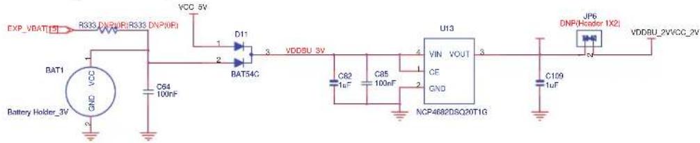
The SAMA5D4-XULT board requires a battery (3V lithium battery type CR1225 or equivalent) in order to permanently power the backup part of the SAMA5D4 device (refer to SAMA5D4 Series data sheet).
To avoid losing data and saved registers, the board must be powered on when replacing the battery.
Figure 4-4. VBAT Powering Scheme Option
text_image
EXP_VBAT[5] R333 DN20R1RS33 DNP90F1 VCC 5V BAT1 1 2 3 VDDBU 3V GND VCC C64 100nF C82 1uF C85 100nF U13 VIN VOUT CE GND NCP4682DSQ20T1G JP6 DNP(Header 1X2) VDDBU_2VVCC_2V Battery Holder_3V4.2.2.8 Power Supply Control
In the ACT8865, three DCDCs (1.8V, 1.2V, 3.3V) and two LDO outputs are available.
All ACT8865 outputs can be controlled by the TWI interface through software.
The three DCDCs outputs can be enabled or disabled by the SAMA5D44 SHDN output:
- SHDN = 0: The DCDCs output is disabled.
- SHDN = 1: The DCDCs output is enabled.
Two push buttons are also available:
- Wakeup push button: When pressed, the ACT8865 power outputs are restarted if the ACT8865 is in shutdown mode.
- Reset push button: When pressed, the ACT8865 transfers the reset signal to NRST_3V3, and then to NRST_2V for the MPU by using a resistor divider.
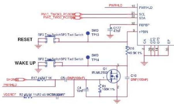
4.2.3 Reset Circuitry
The reset sources for SAMA5D4-XULT board are:
• Power-on reset from the Power Management Unit (PMIC)
- Push button reset BP3
• External reset from Arduino connectors
• JTAG or EDBG reset from an in-circuit emulator
Figure 4-5. Reset/Wakeup and Shutdown Control
text_image
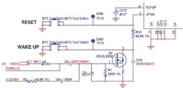
PWRHLD 15 PWRHLD 21 SCL 22 SDA 32 REFBP 9 rPBIN CA 29 CQ1 28 CQ2 14 G23 16 EP RESET SP3 Tact SwitchBP3 Tact Switch SMD TP13 R16 49.9K 1% R17 1kR17 1K C5 DNP(100nF) IRLML2502 Q1 1 C4 10nF R1 100K 1% C10 DNP(100nF) WAKE UP SHON PWMHLD VDDREF R2 49.9K 1%R2 49.9KCB8006nF4.2.4 Clock Circuitry
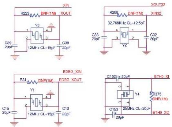
The SAMA5D4-XULT board includes four clock sources:
• Two clocks are alternatives for the SAMA5D44 processor (12 MHz, 32 kHz)
• One crystal oscillator used for the Ethernet RMII chip (25 MHz)
• One crystal oscillator used for the EDBG (12 MHz)
Figure 4-6. Clock Circuitry
4.2.5 Memory
4.2.5.1 Memory Organization
The SAMA5D4 features a DDR/SDR memory interface and an External Bus Interface (EBI) to permit interfacing to a wide range of external memories and to almost any kind of parallel peripheral.
This section describes the memory devices that equip the SAMA5D4-XULT board.
4.2.5.2 DDR2/SDRAM
- Two DDR2/SDRAM (MT47H128M16 - 2 Gb - 16 Meg x 16 x 8 banks) are used as main system memory. The board provides 4 Gb on-board, soldered DDR2 (double data rate) SDRAM. The memory bus is 32 bits wide and operates with a frequency of up to 176 MHz.
Figure 4-7. DDR2
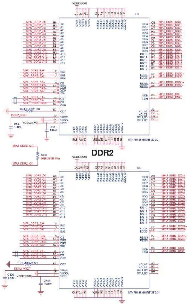
text_image
Circuit diagrams of DDR2 and VDDI000R components with labeled pins, power connections, and component values4.2.5.3 DDR\_CALP and DDR\_CALN Analog Inputs
Two specific analog inputs, DDR_CALP and DDR_CALN, are used to calibrate all DDR I/Os.
Figure 4-8. DDR_CALP and DDR_CALN Analog Inputs

text_image
MPU DDR2 BA0 C15 DDR BA0 MPU DDR2 BA1 D14 DDR BA1 MPU DDR2 BA2 G13 DDR BA2 VDDIODOR R244 200R 1%R244 200R 1% R243 200R 1%R243 200R 1% C39 DDR CALN DDR_CALP DDR2 VREF K12 DDR VREF C97 100nFTable 4-3. DDR_CALN and DDR_CALP
| Memory Type CALP Pull-down CALN Pull-up | ||
| DDR2 200 ohm 200 ohm | ||
| LPDDR2 240 ohm 240 ohm | ||
4.2.5.4 NAND Flash
One 512 MB NAND Flash is connected to the processor.
Figure 4-9. NAND Flash

text_image
Nand Flash R286 10DK 1% R283 10K R285 10DK 1% 3V3_NAND NAND CLE PC18 NAND ALE PC17 NAND HEA PC16 NAND WFn PC14 NAND CEa PC15 NAND RDY PC16 R282 2R (NAND WPn) R288 DNP(100K 1%) R267 0R C43 100nF C45 100nF C41 100nF C44 100nF U9 CLE ALE FE WF VE H/R WP NCL16 NCL19 NCL20 NCL21 NCL22 NCL23 NCL24 NCL25 NCL26 NCL27 NCL28 NCL29 NCL30 NCL31 NCL32 NCL33 NCL34 NCL35 NCL36 NCL37 NCL38 NCL39 NCL40 NCL41 NCL42 NCL43 NCL44 NCL45 NCL46 NCL47 NCL48 NCL49 NCL50 NCL51 NCL52 NCL53 NCL54 NCL55 NCL56 NCL57 NCL58 NCL59 NCL60 NCL61 NCL62 NCL63 NCL64 NCL65 NCL66 NCL67 NCL68 NCL69 NCL70 NCL71 NCL72 NCL73 NCL74 NCL75 NCL76 NCL77 NCL78 NCL79 NCL80 NCL81 NCL82 NCL83 NCL84 NCL85 NCL86 NCL87 NCL88 NCL89 NCL90 NCL91 NCL92 NCL93 NCL94 NCL95 NCL96 NCL97 NCL98 NCL99 NCL100 NVCC 1 12 VCC 2 37 VCC 3 34 VCC 4 39 VSS 1 13 VSS 2 38 VSS 3 25 VSS 4 48 NVCC_I/OI PC5 29 NAND I/OI PC6 NAND I/OI PC7 NAND I/OI PC8 NAND I/OI PC9 NAND I/OI PC10 NAND I/OI PC11 NAND I/OI PC12 NAND I/OI PC13 SV3_NANDXVG_NANDVCC_3V3 MT29F4C0BABAADWPC-E4.2.5.5 CS Disable
The SAMA5D44 device boots according to the following sequence:
- D CARD connected on MCI1
- Optional Dataflash connected on NPCS0 SPI0
- 8-bit NAND Flash connected to D0-D7
In this sequence, the first device found with bootable contents is selected as the boot source. The others are disregarded.
On-board jumpers (JP7, JP8) control the selection (CS#) of the on-board bootable memory components (NAND Flash and Serial DataFlash) using a non-inverting 3-state buffer.
Figure 4-10. CS Disable

text_image
Nand & SPI Flash CS VCC 3V3 C40 100nF U10 R291/280/281 0R VCC 5 JPS DNP Header 1X2 JPR8 DNP(UX/PLR) AT25_SP18_C03_PC3AT25_SP16_NC2P83_PC3 SPI Flash CS JP7 Header 1X2 JP17 JUMPER U0G1_LX8 C42 100nF U8 VCC 5 JND NL17SZ1260FT2G C40 100nF U8 VCC 5 JND NL17SZ1250F13G NAND_CF-PC15NAND_NC23_PC15 NAND Flash CS The jumper JP2 must be populated next the reset buttonThe rule of operation is:
JP7 = OFF (default) → enable normal boot from NAND Flash (or serial DataFlash if mounted)
JP7 = ON → booting from optional serial DataFlash or NAND Flash is disabled
JP8 (optional) also controls the serial DataFlash if mounted.
Refer to the SAMA5D4 Series datasheet for more information on standard boot strategies and sequencing.
4.2.6 Additional Memories
4.2.6.1 Serial Data Flash (optional)
The SAMA5D44 provides two high-speed Serial Peripheral Interface (SPI) controllers. One port is used to interface with the optional on-board serial DataFlash.
The four main signals used in the SPI are Clock, Data In, Data Out, and Chip Select. The SPI is a serial interface similar to the I²C bus interface but with three main differences:
It operates at a higher speed.
• Transmit and receive data lines are separate.
• Device access is chip select-based instead of address-based.
Figure 4-11. Optional Serial DataFlash

text_image
SPI Flash A725 SPI0 MOSI PC1 A725 SPI0 MSO PC0 A725 SPI0 SPCK PC2 A725 SPI0 CSO PC3 R211 100K 1% R211 100K 1% VCC 3V3 U5 SI VCC SO WP SCK FOLD CS GND DNP(AT25DF521A) C34 100nF4.2.6.2 Serial EEPROM with Unique MAC Address
The SAMA5D4-XULT board embeds one Atmel AT24MAC402/602 EEPROM using a TWI0 interface.
The AT24MAC402/602 provides 2048 bits of Serial Electrically-Erasable Programmable Read-Only Memory (EEPROM) organized as 256 words of eight bits each and is accessed via an I²C-compatible (2-wire) serial interface. In addition, the AT24MAC402/602 incorporates an easy and inexpensive method to obtain a globally unique MAC or EUI address (EUI-48 or EUI-64).
The EUI-48/64 addresses can be assigned as the actual physical address of a system hardware device or node, or it can be assigned to a software instance. These addresses are factory-programmed by Atmel and permanently write-protected in an extended memory block located outside of the standard 2-Kbit memory array.
In addition, the AT24MAC402/602 provides the value-added feature of a factory-programmed, guaranteed unique 128-bit serial number located in the extended memory block (same area as the EUI address values).
The EEPROM device is used as a "soft label" to store board information such as chip type, manufacture name and production date, using the last two 16-byte blocks in memory.

WARNING
The information contained in these blocks should not be modified.
Figure 4-12. EEPROM
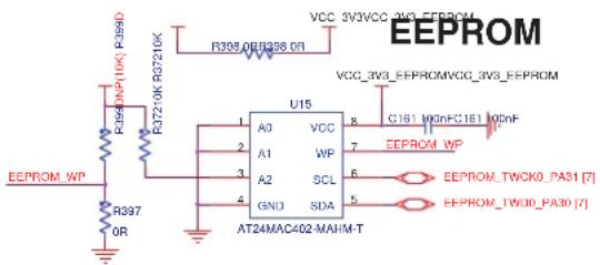
text_image
EEPROM R398.0RR398.0R VCC_3V3VCC_3V3_EEPROM R399.0DP(10K) R399.0 R722.0K R372.10K R397.0R U15 A0 VCC A1 WP A2 SCL GND SDA AT24MAC402-MAHM-T G161 100nFC161 100nF EEPROM_WP EEPROM_TWCK0_PA31 [7] EEPROM_TWJ0D_PA30 [7]4.2.7 High-Speed Multimedia Card Interface (HSMCI)
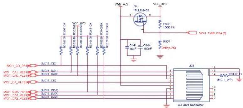
4.2.7.1 Multimedia Card Interface (MCI)
The SAMA5D4-XULT board has two high-speed Multimedia Card interfaces (MCIs) that support the multimedia card (MMC) Specification V4.3, the SD Memory Card Specification V2.0 and the SDIO V1.1 specification:
- MCI0 interface based on a 7-pin interface (clock, command, 4-bit data, power lines).
- MCI1 Interface based on a 7-pin interface (clock, command, 4-bit data, power lines).
4.2.7.2 HSMCI Card Connector
A standard MMC/SD card (push and click type) connector, connected to MCI1, is mounted on the top side of the board. It features a push-lock / push-eject mechanism and a card detection switch.
A micro SD card (push and click type) connector, connected to MCI0, is mountable as an option on the bottom side of the board.
Figure 4-13. HSMCI0 & HSMCI1
text_image
VDD_MCH D4 IRLML8432 VCC_JW3 R548 100K 1% P357 DNP(4.7kΩ) MOH_PWR_PE4 [9] C141 10uF C144 100vF J24 18 15 14 13 12 11 10 R560R_PE (MCH_WP3) R560R_PE4 MCH_CDA_PE18# MCH_DAD_PE23# MCH_CDA_PE22# MCH_CCK_PE19# MCH_DAD_PE21# MCH_DAD_PE20# MCH_CCK_PE18# MCH_CDA_PE17# MCH_DAD_PE22# MCH_DAD_PE21# MCH_CCK_PE19# MCH_CDA_PE20# MCH_DAD_PE21# MCH_DAD_PE20# MCH_CCK_PE19# MCH_CDA_PE20# MCH_DAD_PE21# MCH_DAD_PE20# MCH_CCK_PE19# MCH_CDA_PE20# MCH_DAD_PE21# MCH_DAD_PE20# MCH_CCK_PE19# MCH_CDA_PE20# MCH_DAD_PE21#SD/MMCPlus CARD INTERFACE - MCI1

text_image
I10589 R1 10000K R17368 R17368 R15968K R14159 R14159 VCC_3V3 R142 R142 R163 R163/CK R1D4 D J9 DAT0 DAT1 DAT2 DAT3 CMG CLK VDD VSS CD PGND P0ND 1 P0ND 2 P0ND 3 NC 1 NC 2 12 13 14 15 HCIB_DA3_P0X8 HCIB_DA1_P0X8 HCIB_DA2_P0X8 HCIB_DA3_P0X8 HCIB_CU3_P0X8 HCIB_CU4_P0X8 HCIB_CU5_P0X8 HCIB_CU6_P0X8 HCIB_CU7_P0X8 HCIB_CU8_P0X8 HCIB_CU9_P0X8 HCIB_CU10_P0X8 HCIB_CU11_P0X8 C29 C30 10uF 10uF DNP(MicroSD Card Connector)Micro SD CARD INTERFACE - MCI0
4.2.8 Communication Interfaces
The SAMA5D4-XULT board is equipped with EMAC and USB Host/Device communication interfaces.
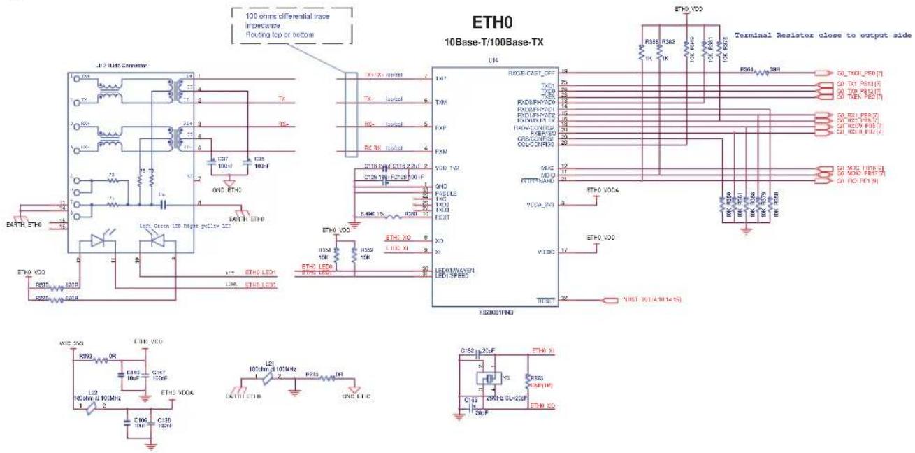
4.2.8.1 Ethernet 10/100 (EMAC) Port
The SAMA5D4-XULT board contains a MICREL PHY device (KSZ8081) operating at 10/100 Mb/s. The board supports RMII interface modes. The Ethernet interface consists of two pairs of low-voltage differential pair signals designated from GRX± and GTX± plus control signals for link activity indicators. These signals can be used to connect to a 10/100 Base-T RJ45 connector integrated on SAMA5D4-XULT board.
Additionally, for monitoring and control purposes, LED functionality is carried on the RJ45 connectors to indicate activity, link, and speed status information.
For more information about the Ethernet controller device, refer to the MICREL KSZ8081RN controller manufacturer's datasheet.
Figure 4-14. Ethernet
text_image
100 ns differential trace impedance Routing top or bottom J1 2 RADS Connect J1 2 RADS EARTH ETH ETH0 VDD R935 R935 COSF L20 100mA di 100MHz C106 10Hz C145 10uF C147 10uF ETH0 VDD L21 100mA di 100MHz C106 10Hz C145 10uF ETH0 LED ETH0 LED ETH0 LED ETH0 LED ETH0 LED ETH0 LED ETH0 LED ETH0 LED ETH0 LED ETH0 LED ETH0 LED ETH0 LED ETH0 LED ETH0 LED ETH0 LED ETH0 LED ETH0 LED ETH0 LED ETH0 LED ETH0 LED ETH0 LED ETH0 LED ETH0 LED ETH0 LED ETH0 LED ETH0LED ETH0LED ETH0LED ETH0LED ETH0LED ETH0LED ETH0LED ETH0LED ETH0LED ETH0LED ETH0LED ETH0LED ETH0LED ETH0LED ETH0LED ETH0LED ETH0LED ETH0LED ETH0LED ETH0LED ETH0LED ETH0LED ETH0LED ETH0LED ETH0LED ETH0L THB THB THB THB THB THB THB THB THB THB THB THB THB THB THB THB THB THB THB THB THB THB THB THB THB THB THB THB THB THB THB THB THB THB4.2.8.2 USB Host/Device A, B & C
The SAMA5D4-XULT board features three USB communication ports:
• USB Host B/C High- and Full-speed Interface
- Two USB host stacked type A connectors.
• USB Host/Device A Interface
One USB device standard micro-AB connector. This port has a VBUS detection function made through the resistor ladder R218 and R214.
Figure 4-15. USB Host & Device Interface

text_image
USB A USB VISUS SV [4] R218 100K 13/1218 100K 13 C56 20pF R214 200K USBA_VSUS_PE31 [9] V_BUS 1 DH 2 DP 3 D1 4 DND 5 J11 MicroUSB Alt Connector L12 183ohm at 100Gb 1 2 EARTH_USB_A EARTH_USB_A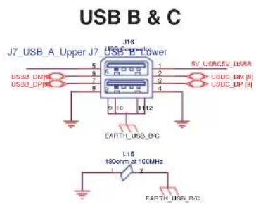
text_image
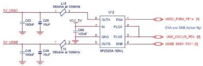
USB B & C J7_USB_A_Upper_J7_USB_B_Upper J15 USB_DIN USB_DIN 5 6 7 8 9 10 11/12 5V_USB_CEV_USB_R 5V_USB_DM_R 5V_USB_DP_R L15 180ohm at 100MHz FARTH_USB_B/C FARTH_USB_B/CThe two USB Host ports are equipped with 500 mA high-side power switch for self-powered and bus-powered applications.
text_image
5V USSC C43 100nF C45 10uF L18 180ohm at 100MHz VCC_5V C68 100nF C46 100nF C49 10uF L18 180ohm at 100MHz U12 OUTA ENA IN FLGA GNG FLGB OUTB ENB SP2526A-1EN-L 1 2 3 4 USGC_EN5V_PE14 [9] ENA and ENB Active High* USB_CVCUR_PE0 [9] USSB_EN5V_PE11 [9]4.2.9 LCD TFT Interface
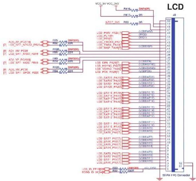
4.2.9.1 LCD
The SAMA5D4 provides 24 bits of data and control signals to the LCD interface. Other signals are used to control the LCD and are available on connector J2: TWI, SPI, 2 GPIOs for interrupt, 1-Wire and power supply lines.
4.2.9.2 LCD Expansion Header
J2 is a 1.27mm pitch 50-pin header; it gives access to the LCD signals.
Figure 4-16. LCD Expansion Header Interface
text_image
VCC_5V VCC_XV R416 DNP(OR) R417 OR NRS7 WNS R33 OR LCD PWM PA24/7 LCD_PLT09 LCD_PPE8 LCD_TWDCU PA23 LCD_DSP PA26/7 LCD_CEN PA26/7 LCD_NSNC PA24/7 LCD_VSYNC PA26/7 LCD_PCK PA28/7 LCD_DAT3 PA28/7 LCD_DAT2 PA28/7 LCD_DAT1 PA28/7 LCD_DAT1 PA13/7 LCD_DAT1 PA13/7 LCD_DAT1 PA13/7 LCD_DAT1 PA13/7 LCD_DAT1 PA13/7 LCD_DAT1 PA13/7 LCD_DAT1 PA13/7 LCD_DAT1 PA13/7 LCD_DAT1 PA13/7 LCD_DAT1 PA13/7 LCD_DAT1 PA13/7 LCD_DAT1 PA13/ LCD_DAT1 PA13/7 LCD_DAT1 PA13/7 LCD_DAT1 PA13/7 LCD_DAT1 PA13/7 LCD_DAT1 PA13/7 LCD_DAT1 PA13/7 LCD_DAT1 PA13/7 LCD_DAT1 PA13/7 LCD_DAT1 PA13/7 LCD_DAT1 PA13/7 LCD_DAT1 PA13/7 LCCOEN (OR) LCCOEN (OR) LCCOEN (OR) LCCOEN (OR) LCCOEN (OR) LCCOEN (OR) LCCOEN (OR) LCCOEN (OR) LCCOEN (OR) LCCOEN (OR) LCCOEN (OR) LCCOEN (OR) LCCOEN (OR) LCCOEN (OR) LCCOEN (OR) LSCOEN (OR) LSCOEN (OR) LSCOEN (OR) LSCOEN (OR) LSCOEN (OR) LSCOEN (OR) LSCOEN (OR) LSCOEN (OR) LSCOEN (OR) LSCOEN (OR) LSCOEN (OR) LSCOEN (OR) LSCOEN (OR) LSCOEN (OR) LSCOENO (OR) LSCOENO (OR) LSCOENO (OR) LSCOENO (OR) LSCOENO (OR) LSCOENO (OR) LSCOENO (OR) LSCOENO (OR) LSCOENO (OR) LSCOENO (OR) LSCOENO (OR) LSCOENO (OR) LSCOENO (OR) LSCOENO (OR) LSCOENO (ON) LSCOENO (ON) LSCOENO (ON) LSCOENO (ON) LSCOENO (ON) LSCOENO (ON) LSCOENO (ON) LSCOENO (ON) LSCOENO (ON) LSCOENO (ON) LSCOENO (ON) LSCOENO (ON) LSCOENO (ON) LSCOENO (ON) LSCOENO (ON) S2 S1 LCD ID: PFE0000000000000000000000000000000000000000000000000000000000000000000000000000000000000000000000000000 5D Pin FPC Connector4.2.9.3 LCD Power
In order to operate correctly out of the processor with various LCD modules, two voltage lines are available: 3.3V and 5 VCC (default), both selected by 0R resistors R416 and R417.
Figure 4-17. LCD Power
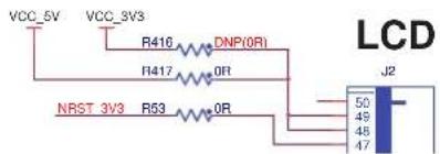
text_image
VCC_5V VCC_3V3 R416 DNP(0R) R417 0R NRST 3V3 R53 0R LCD 50 49 48 47 J24.2.10 HDMI Transmitter Interface
The SAMA5D4-XULT board features the Silicon Image SiI9022ACUN device to convert video signals to the HDMI standard.
It features the following:
- Compliance
— HDMI 1.2a, Simply HD, DVI 1.0
Digital Video Output - Integrated TMDS core
DTV resolution support - 480i/576i/480p/576p/720p/1080i/1080p - PC resolution support - VGA/XGA/SXGA/WSXGA/UXGA
- Flexible interface to HD MPEG decoders
- Integrated YCbCr → RGB conversion
4:2:2 → 4:4:4 up-converter
Digital Audio Output
— DVD-Audio support through 4 x I2S inputs
– Supports 2-ch 192 kHz or 8-ch 96 kHz
Supports IEC60958 2-ch PCM or IEC61937 compressed audio (Dolby Digital, DTS, etc.)
— Industry-standard S/PDIF input, Integrated MCLK generator
Power Management
- 1.2V and 1.8V cores provide low-power operation
- Flexible power-down modes
Figure 4-18. HDMI Interface

text_image
HDMI 100 ohms differential trace impedance Racing top or action VCC GV F1 1012L16D-2 RB-EN 560TR VCC_VS_HDMI F25 2.8K 1% F24 2.8K 1% HDM_SCL HDM_SCL HDM_1 HDM_1 HDM_1 HDM_1 HDM_1 HDM_1 HDM_1 HDM_1 HDM_1 HDM_1 HDM_1 HDM_1 HDM_1 HDM_1 HDM_1 HDM_1 HDM_1 HDM_1 HDM_1 HDM_1 HDM_2 HDM_2 HDM_2 HDM_2 HDM_2 HDM_2 HDM_2 HDM_2 HDM_2 HDM_2 HDM_2 HDM_2 HDM_2 HDM_2 HDM_2 HDM_2 HDM_2 HDM_2 HDM_2 HDM_2 HDM_3 HDM_3 HDM_3 HDM_3 HDM_3 HDM_3 HDM_3 HDM_3 HDM_3 HDM_3 HDM_3 HDM_3 HDM_3 HDM_3 HDM_3 HDM_3 HDM_3 HDM_3 HDM_3 HDM_3 HDM_4 HDM_4 HDM_4 HDM_4 HDM_4 HDM_4 HDM_4 HDM_4 HDM_4 HDM_4 HDM_4 HDM_4 HDM_4 HDM_4 HDM_4 HDM_4 HDM_4 HDM_4 HDM_4 HDM_4 HDM_5 HDM_5 HDM_5 HDM_5 HDM_5 HDM_5 HDM_5 HDM_5 HDM_5 HDM_5 HDM_5 HDM_5 HDM_5 HDM_5 HDM_5 HDM_5 HDM_5 HDM_5 HDM_5 HDM_5 HDM_6 HDM_6 HDM_6 HDM_6 HDM_6 HDM_6 HDM_6 HDM_6 HDM_6 HDM_6 HDM_6 HDM_6 HDM_6 HDM_6 HDM_6 HDM_6 HDM_6 HDM_7 HDM_7 HDM_7 HDM_7 HDM_7 HDM_7 HDM_7 HDM_7 HDM_7 HDM_7 HDM_7 HDM_7 HDM_7 HDM_7 HDM_7 HDM_7 HDM_7 HDM 800A HOMI 100MHz 100MHz 100MHz 100MHz 100MHz 100MHz 100MHz 100MHz 100MHz 100MHz 100MHz 100MHz 100MHz 100MHz 100MHz 100MHz 100MHz 100MHz 100MHz 100MHz 100kHz 100kHz 100kHz 100kHz 100kHz 100kHz 100kHz 100kHz 100kHz 100kHz 100kHz 100kHz 100kHz 100kHz 100kHz 100kHz 100kHz 100kHz 100kHz 100kHz 100kV HOMI 100MHz 100MHz 100MHz 100MHz 100MHz 100MHz 100MHz 100MHz 100MHz 100MHz 100MHz 100MHz 100MHz 100kHz 100kHz 100kHz 100kHz 100kHz 100kHz 100kV HOMI 100MHz 100MHz 100MHz 100MHz 100MHz 100MHz 100MHz 100MHz 100MHz 100kHz 100kHz 100kHz 100kHz 100kHz 100kHz 10kV HOMI 1kV HOMI 2kV HOMI 3kV HOMI 4kV HOMI 5kV HOMI 6kV HOMI 7kV HOMI 8kV HOMI 9kV HOMI 1kV HOMI 2kV HOMI 3kV HOMI 4kV HOMI 5kV HOMI 6kV HOMI 7kV HOMI 8kV HOMI 9kV HOMI 1kV HOMI 2kV HOMI 3kV HOMI 4kV HOMI 5kVI HOMI 6kVI HOMI 7kVI HOMI 8kVI HOMI 9kVI HOMI 1kVI HOMI 2kVI HOMI 3kVI HOMI 4kVI HOMI 5kVI HOMI 6kVI HOMI 7kVI HOMI 8kVI HOMI 9kVI HOMI4.2.11 Indicators
There are two LEDs on the SAMA5D4-XULT board that can be controlled by the user:
The red LED provides an indication that power is supplied to the board and is controlled via software.
• The blue LED is controlled via GPIO pins.
Figure 4-19. LED Indicators

text_image
LED LED USER PE15 R14E 470R D10 BLUE PD30 LED POWER PD30 R144 100K 1%R144 100K 1% Q3 2 IRLML2502 TP16TP19 R136 470R DB RED VOC 3W34.2.12 Push Button Switches
The SAMA5D4-XULT features three push buttons:
One board Reset button (BP3). When pressed and released, it causes a power-on reset of the board.
• One Wakeup push button to exit the processor from low-power mode (BP2).
• One User momentary push button (BP1).
Figure 4-20. Push Buttons
text_image
RESET BP3 Tap-SwitchBP3 Tap Switch SMD TP13 C177 47nF 32 REFBP nPBN GA Q1 Q2 Q3 EP R16 49.9K 1% GND WAKE UP BP2 Tap-SwitchBP2 Tap Switch SMD TP14 3 IRLVL2502 Q1 1 C10 DNP(100nF) C4 10nF R1 100K 1% C6 100nF R17 R617 JK [9] SHDN FWRHD VDDREF R2 43.9K 1% C5 DNP(100nF) C6 100nF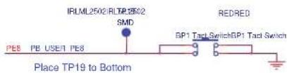
text_image
IRLML2502/IRL7P2502 SMD REDRED PEB PE USE1 PE8 BP1 Tap SwitchBP1 Tap Switch Place TP19 to BottomUSER BUTTON
4.2.13 Debug Interfaces
The SAMA5D4-XULT board includes a JTAG, a Debug serial COM port and an EDBG interface port, to provide debug level access to the SAMA5D4.
4.2.13.1 Debug JTAG
A 2x10-pin JTAG header is provided on the SAMA5D4-XULT board to facilitate the software development and debugging by using various JTAG emulators. The interface signals have a voltage level of 3.3V.
Figure 4-21. JTAG Interface

text_image
JTAG VCC_3V3 VCC_3V3 R224 100K 1% R222 100K 1% R227 100K 1% R217 100K 1% R220 IN823 0P MTRST [7] TDI [7,14] TWS [7,14] TDX [7,14] TDO [7,14] NRST_3V3 [4,12,14,15] J13 J1 6 8 10 12 14 16 18 20 Hostor 2X10 R235 IN835 0P R250 IN850 0P4.2.13.2 DBGU
The SAMA5D4-XULT board has a dedicated serial port for debugging, which is accessible through the 6-pin male header J1. Various interfaces can be used as USB/Serial DBGU port bridge, such as FTDI TTL-232R USB to TTL serial cable or basic breakout board for the RS232/USB converter.
Figure 4-22. DBGU Interface

text_image
DEBUG DRGU_CTS3_PE5A DCGU_TXD3_PE1704 DCGU_RXD3_PE1805 DCGU_RTS3_PE2401 CTS3 TXD3 TXD5 RTS3 P102NP000 P115K_RU P128K_BL P157NP000 P143NP000 VCCNIP000 P132NP000 J1 1 2 3 4 5 Header 1X6R13 and R14 are optional (not implemented) resistors that can be used for power selection. Power can be delivered either by the SAMA5D4-XULT board or by the debug interface tool. To avoid malfunction between the debug interface (e.g., FTDI) and the on-board power system, ensure that the voltage level selected corresponds to application requirements.
4.2.14 Embedded Debugger (EDBG) Interface
The Atmel Embedded Debugger (EDBG) ^(1) is an intuitive plug-and-play solution which adds full programming and debugging support to embedded hardware kits containing Atmel microcontrollers. It enables seamless integration between the target hardware and the Atmel Studio front end.
In addition to the Virtual COM port which provides a UART bridge to the target device, the EDBG provides a Data Gateway Interface, through which the target device and host PC can communicate, facilitating high-level application debugging, monitoring, graphing and logging of system information in real-time.
The EDBG is based on the Atmel UC3A4 high-performance low-power 32-bit AVR microcontroller running at up to 60 MHz. The device includes an on-chip USB 2.0 high-speed hardware module with dedicated DMA channels, making it ideal for data communications.
By default, the EDBG is in Reset state and not usable. To use the EDBG interface, remove the jumper JP1. To avoid any conflict with the debug signals, do not use the JTAG and EDBG at the same time.
Figure 4-23. EDBG Interface

text_image
EDBG_TWI EDBG U1 MEDIUM/MEDIUM/MEDIUM/IC JTAG VCC EDBG C22 C103 C196 C100 C188 C22 C103 C196 C100 C188 VCC EDBG C22 C103 C196 C100 C188 C22 C103 C196 C100 C188 VCC EDBG C22 C103 C196 C100 C188 C22 C103 C196 C100 C188 VCC EDBG C22 D4 R23 R24 R25 R26 R27 R28 R29 R30 R31 R32 R33 R34 R35 R36 R37 R38 R39 R40 R41 R42 R43 R44 R45 R46 R47 R48 R49 R50 R51 R52 R53 R54 R55 R56 R57 R58 R59 R60 R61 R62 R63 R64 R65 R66 R67 R68 R69 R70 R71 R72 R73 R74 R75 R76 R77 R78 R79 R80 R81 R82 R83 R84 R85 R86 R87 R88 R89 R90 R91 R92 R93 R94 R95 R96 R97 R98 R99 R100 VCC EDBG 500A 50A 50A 50A 50A 50A 50A 50A 50A 50A 50A 50A 50A 50A 50A 50A 50A 50A 50A 50A 50A 50A 50A 50A 50A 50A 10KΩ 1.5Ω 1.5Ω 1.5Ω 1.5Ω 1.5Ω 1.5Ω 1.5Ω 1.5Ω 1.5Ω 1.5Ω 1.5Ω 1.5Ω 1.5Ω 1.5Ω 1.5Ω 1.5Ω 1.5Ω 1.5Ω 1.5Ω 1.5Ω 1.0Ω 1.5Ω 1.5Ω 1.5Ω 1.5Ω 1.5Ω 1.5Ω 1.5Ω 1.5Ω 1.5Ω 1.5Ω 1.5Ω 1.5Ω 1.5Ω 1.5Ω 1.5Ω 1.5Ω 1.5Ω 1.5Ω 1.5Ω 1.2Ω 1.5Ω 1.5Ω 1.5Ω 1.5Ω 1.5Ω 1.5Ω 1.5Ω 1.5Ω 1.5Ω 1.5Ω 1.5Ω 1.5Ω 1.5Ω 1.5Ω 1.5Ω 1.5Ω 1.5Ω 1.5Ω 1.5Ω 1.3Ω 1.5Ω 1.5Ω 1.5Ω 1.5Ω 1.5Ω 1.5Ω 1.5Ω 1.5Ω 1.5Ω 1.5Ω 1.5Ω 1.5Ω 1.5Ω 1.5Ω 1.3Ω 1.5Ω 1.5Ω 1.5Ω 1.5Ω 1.3Ω 1.5Ω 1.5Ω 1.3Ω 1.5Ω 1.3Ω 1.3Ω 1.3Ω 1.3Ω 1.3Ω 1.3Ω 1.3Ω 1.3Ω 1.3Ω- Device and Ordering Information—The EDBG is a factory-programmed AT32UC3A4256J-C1UR standard microcontroller with ordering code AT32UC3A4256HHB-C1UR. For further information please contact edbg@atmel.com.
4.2.15 Expansion Ports
4.2.15.1 Arduino
Five 8-pin, one 6-pin, one 10-pin and one 36-pin headers (J6, J7, J8, J14, J15, J17, J18, J19) are provided on the SAMA5D4-XULT board to enable the PIO connection of various expansion cards. These headers' physical and electrical implementation match the Arduino R3 extension ("shields") scheme.
Due to multiplexing, different signals can be provided on each pin.
Figure 4-24. Expansion Boards Connectors

text_image
Expansion Boards Connectors VCC 3V3 EXP VBAT4 R1700 INR 1S 3 NRSI_3V3/4/5/6/7/8/9/10/11/12/13/14/15/16/17/18/19/20/21/22/23/24/25/26/27/28/29/30/31/32/33/34/35/36/37/38/39/40/41/42/43/44/45/46/47/48/49/50/51/52/53/54/55/56/57/58/59/60/61/62/63/64/65/66/67/68/69/70/71/72/73/74/75/76/77/78/79/80/81/82/83/84/85/86/87/88/89/90 J6 J7 J8 J9 J10 J11 J12 J13 J14 J15 J16 J17 J18 J19 J20 J21 J22 J23 J24 J25 J26 J27 J28 J29 J30 J31 J32 J33 J34 J35 J36 J37 J38 J39 J40 J41 J42 J43 J44 J45 J46 J47 J48 J49 J50 J51 J52 J53 J54 J55 J56 J57 J58 J59 J60 J61 J62 J63 J64 J65 J66 J67 J68 J69 J70 J71 J72 J73 J74 J75 J76 J77 J78 J79 J80 J81 J82 J83 J84 J85 J86 J87 J88 J89 J90 J91 J92 J93 J94 J95 J96 J97 J98 J99 J100 EXP PE23 [5] EXP XPRO PE18 [6] EDBG_DGI_GPIO1 [4] EXP XPRO_PE18 [8] EDBG_DGI_GPIO1 [4] EXP PDQ2 [7] EXP XPRO_PC1 [8] EXP_PE20 [8] EDBG_DGI_GPIO1 [4] EXP PE15 [6] EDBG_DGI_GPIO1 [4] EXP XPRO_PC2 [8] EXP_PBI [7] EXP XPRO_PC2 [8] EXP XPRO_PC0 [8] EXP PE10 [6] EDBG_DGI_GPIO1 [4] EXP XPRO_PC3 [8] EXP TWO 3D PA3F [7] EXP TWO 3D PA3I [7] EXP XPRO_PC2 [8] EXP PE27 [5] EXP XPRO_PE26 [8] EXP XPRO_PD17 [9] EXP PD16 [9] EXP XPRO_PD13 [9] EXP_PD-2 [9] EXP TWO 3D PA3F [7] EXP TWO 3D PA3I [7] EXP XPRO_PC2 [8] EXP PE0BHK OR 3H P200 R323 R324 R325 R327 R328 R329 R330 R331 R332 R333 R334 R335 R336 R337 R338 R339 R340 R341 R342 R343 R344 R345 R346 R347 R348 R349 R350 R351 R352 R353 R354 R355 R356 R357 R358 R359 R360 R361 R362 R363 R364 R365 R366 R367 R368 R369 R370 R371 R372 R373 R374 R375 R376 R377 R378 R379 R380 R381 R382 R383 R384 R385 R386 R387 R388 R389 R390 R391 R392 R393 R394 R395 R396 R397 R398 R400 R401 R402 R403 R404 R405 R406 R407 R408 R409 R410 R411 R412 R413 R414 R415 R416 R417 R418 R419 R420 R421 R422 R423 R424 R425 R426 R427 R428 R429 R430 R431 R432 R433 R434 R435 R436 R437 R438 R439 R440 R441 R442 R443 R444 R445 R446 R447 R448 R449 R450 R451 R452 R453 R454 R455 R456 R457 R458 R459 R460 R461 WBO 2VXP EXP 5V 1VBO 2VXP EXP 5V 1VBO 2VXP EXP 5V 1VBO 2VXP EXP 5V 1VBO 2VXP EXP 5V 1VBO 2VXP EXP 5V 1VBO 2VXP EXP 5V 1VBO 2VXP EXP 5V 1VBO 2VXP EXP 5V 1VBO 2A B D E B G D E D E D E D E D E D E D E D E D E D E D E D E D E D E D E D E D E D E D E D E D E D E D E D E D E D E D E D E D E D E D E D E D E D E D E D E D E D E D E D E D E D E D E D E D E D E D E D E D E D E D F O P P P P P P P P P P P P P P P P P P P P P P P P P P P P P P P P P P P P P P P P P P P P P P P P P P P P P P P P P P P P P P P P P P P P P P P P P P P P P P P P P P P P P P P P P P P P P P P P P P P P A N S T S T S T S T S T S T S T S T S T S T S T S T S T S T S T S T S T S T S T S T S T S T S T S T S T S T S T S T S T S T S T S T S T S T S T S T S T S T S T S T S T S T S T S T S T S T S T S T S T S T S I NST 3V5 100V 1S NST 3V5 100V 1S NST 3V5 100V 1S NST 3V5 100V 1S NST 3V5 100V 1S NST 3V5 100V 1S NST 3V5 100V 1S NST 3V54.2.15.2 Functions Available Through the Arduino Headers
The multiplexing of the SAMA5D44 I/Os (standard parallel I/O and up to three peripheral functions per pin) makes it possible to route alternate signals via Arduino extension headers. To enable these signals, SAMA5D44 PIO multiplexing must be properly configured. For more details, refer to Section 4.3.15 of this document and the section PIO Controller (PIO) in the SAMA5D4 Series datasheet.
In addition, on-board resistors may be unsoldered and moved to an alternate location to enable a different connection.
Table 4-5 to Table 4-11, together with the connector schematics, provide the alternate signals available for use with Arduino connectors.

TIP
How to read the tables
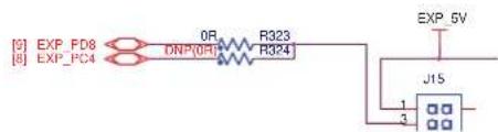
For the example Figure 4-25 and Table 4-4 below, the information provided on alternate signals is read as follows:
Pin 3 of Jxx is normally connected to SAMA5D44 PD8 which has PCK0 as an alternate function.
By unsoldering R323 and soldering it on R324 footprint, pin 3 of J15 will be connected to SAMA5D44 PC4 which has SPI0_NPCS1, MCIO_CK and PCK1 as alternate functions.
Figure 4-25. Jxx Connector
text_image
[EXP_FD8 [EXP_PC4 0R DNP(03) R323 R324 EXP_5V J15 1 2 3
natural_image
Close-up of a blue printed circuit board with visible components and connectors (no readable text or symbols)Table 4-4. Jxx Connector Signals
| Pin No. | SAMA5D44 | PIO | Muxing Alternates On-board Alternates | |||||||
| 3 | PD8 | PCK0 | -- | PC4 | SPI0_NPC | S1 MCI0_CK | PCK1 | |||
Figure 4-26. J6 Connector
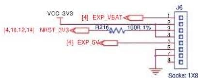
text_image
VCC 3V3 [4] EXP VBAT [4,10,12,14] NRST 3V3 R216 100R 1% [4] EXP 5V J6 1 2 3 4 5 6 7 8 Socket 1X8
natural_image
Close-up of a blue printed circuit board with various electronic components and connectors (no readable text or symbols)Table 4-5. J6 Connector Signals
| Pin No. Signal On-board Alternates | |||||||
| 1 EXP_VBAT ---- | |||||||
| 2 | V | C | C | - | 3 | V | 3 |
| 3 | N | R | S | T | - | 3 | V |
| 4 | V | C | C | - | 3 | V | 3 |
| 5 | E | X | P | - | 5 | V | - |
| 6 | G | N | D | - | - | - | - |
| 7 | G | N | D | - | - | - | - |
| 8 | N | C | - | - | - | - | |
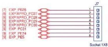
Figure 4-27. J7 Connector
text_image
EXP_P628 EXP/XPRO_PC27 EXP/XPRO_PC28 EXP/XPRO_PC29 EXP/XPRO_PC30 EXP_PC31 EXP_PE24 EXP_PE5 J7 1 2 3 4 5 6 7 8 Socket 1X8
natural_image
Close-up of a blue printed circuit board with connectors and ports (no readable text or symbols)Table 4-6. J7 Connector Signals
| Pin No. | SAMA5D44 PIO Muxing Alternates On-board Alternates | |||||||
| 1 PB28 | SPI2_NPCS3 | TD0 PWMH1 | ---- | |||||
| 2 PC27 | AD0 SPI0_NPCS1 | PWML0 | ---- | |||||
| 3 PC28 | AD1 SPI0_NPCS2 | PWML1 | ---- | |||||
| 4 PC29 | AD2 SPI0_NPCS3 | PWMFI0 | ---- | |||||
| 5 PC30 | AD3 - | PWMH0 | ---- | |||||
| 6 PC31 | AD4 - | PWMH1 | ---- | |||||
| 7 PE24 | NCS0 | RT$3 | ---- | |||||
| 8 | PE5 | A5 | CTS3 | - | - | - | - | - |
Figure 4-28. J8 Connector
text_image
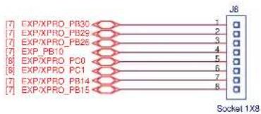
7 EXP/XPRO_PB30 7 EXP/XPRO_PB29 7 EXP_XPRO_PB26 7 EXP_PB10 8 EXP/XPRO_PC0 8 EXP_XPRO_PC1 7 EXP/XPRO_PB14 7 EXP/XPRO_PB15 J8 Socket1X8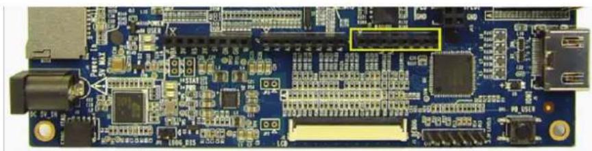
natural_image
Close-up of a blue printed circuit board with various electronic components and connectors (no readable text or symbols)Table 4-7. J8 Connector Signals
| Pin No. | SAMA5D44 PIO Muxing Alternates On-board Alternates | ||||
| 1 PB30 | TWCK2 RF0 | -- | |||
| 2 PB29 | TWD2 RD0 | PWML1 - | |||
| 3 PB26 | PCK0 | RK0 | PWMH0 | - | |
| 4 PB10 | G0_RX2 | PCK2 | PWML1 - | ||
| 5 | PC0 | SPI0_MISO | PWMH2 | ISI_D8 | No DAC available |
| 6 | PC1 | SPI0_MOSI | PWML2 | ISI_D9 | No DAC available |
| 7 | PB14 | G0_TX2 | SPI2_NPCS1 | PWMH0 | No CAN available |
| 8 | PB15 | G0_TX3 | SPI2_NPCS2 | PWML0 | No CAN available |
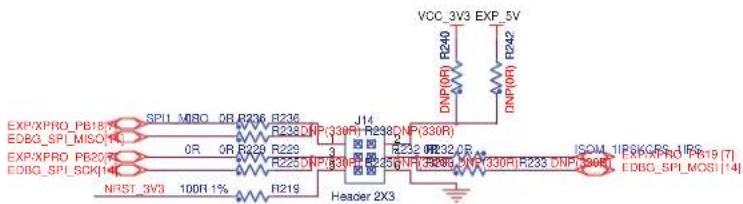
Figure 4-29. J14 Connector
text_image
VOC_3V3 EXP_5V R240 DNP(VR) R242 EXP'XPRO_PB18/7 SP11 MBO 0R R236 R236 EXP'XPRO_PB20/7 0R 0R R226 R229 EXP'SPI_MISO14 R225 DNP(330R) R238 DNP(330R) R232 0R 32.0F R236 DNP(330R) R236 DNP(330R) R236 DNP(330R) R236 DNP(330R) R236 DNP(330R) NRSST_3V3 100R 1% Header 2X3 ISOM_1IP/KCRS_1IPS EXP'XPRO_PB19 [7] EDBG_SPI_MOSI [14]
natural_image
Close-up of a blue printed circuit board with multiple ATmel chip modules and connectors (no readable text or symbols)Table 4-8. J14 Connector Signals
| Pin No. | SAMA5D44 PIO Muxing Alternates | On-board Alternates | EDBG Alternate | ||||||
| 1 | PB18 | SPI1_MISO | D8 | - | - | - | - | - | DGI_SPI |
| 2 | 5V | - | - | - | - | - | - | - | - |
| 3 | PB20 | SPI1_SPCK | D10 | - | - | - | - | - | DGI_SPI |
| 4 | PB19 | SPI1_MOSI | D9 | - | - | - | - | - | DGI_SPI |
| 5 | nRST | - | - | - | - | - | - | - | - |
| 6 | GND | - | - | - | - | - | - | - | - |
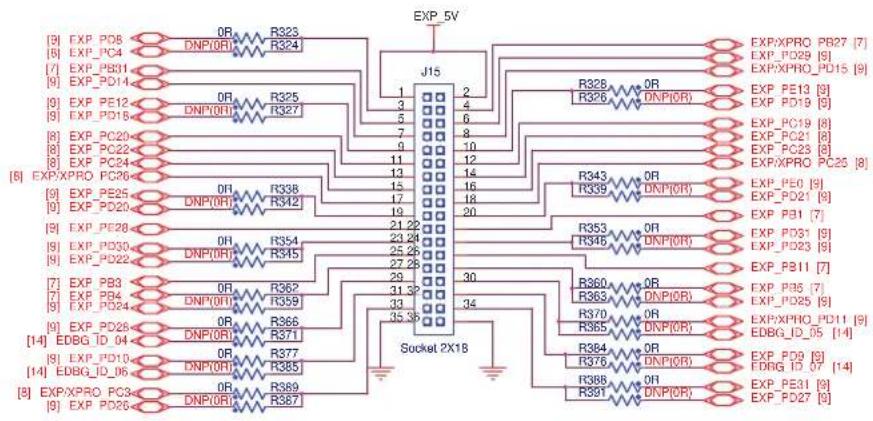
Figure 4-30. J15 Connector
text_image
[3] EXP_PD6 [6] EXP_PC4 [7] EXP_PB31 [9] EXP_PD14 [9] EXP_PE12 [9] EXP_PD15 [8] EXP_PC20 [8] EXP_PC22 [8] EXP_PC24 [8] EXP_XPRO_PC26 [9] EXP_PE25 [9] EXP_PD20 [9] EXP_PE28 [9] EXP_PD30 [9] EXP_PD22 [7] EXP_PB3 [7] EXP_PB4 [9] EXP_PD24 [14] EDBG_ID_04 [14] EDBG_ID_06 [3] EXP_XPRO_PC3 [9] EXP_PD26 J15 1 2 3 4 5 6 7 8 9 10 11 12 13 14 15 16 17 18 19 20 21 22 23 24 25 26 27 28 29 30 31 32 33 34 35 36 Socket 2X18 R323 R324 R325 R327 R338 R342 R354 R345 R362 R359 R366 R371 R377 R385 R389 R387 R326 OR R326 OR DNP(OR) R343 OR R339 OR DNP(OR) R353 OR R345 OR DNP(OR) R360 OR R363 OR DNP(OR) R370 OR R365 OR DNP(OR) R384 OR R376 OR DNP(OR) R388 OR R391 OR DNP(OR) EXP_5V EXP_XPRO PB27 [7] EXP_PD29 [9] EXP_XPRO_PD15 [9] EXP_PE13 [9] EXP_PD19 [9] EXP_PC19 [8] EXP_PC21 [8] EXP_PC23 [8] EXP_XPRO_PC25 [8] EXP_PE0 [9] EXP_PD21 [9] EXP_PB1 [7] EXP_PD31 [9] EXP_PD23 [9] EXP_PB11 [7] EXP_PB5 [7] EXP_PD25 [9] EXP_XPRO_PD11 [9] EDBG_ID_05 [14] EXP_P09 [8] EDBG_ID_07 [14] EXP_PE31 [9] EXP_PD27 [9]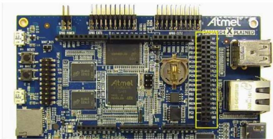
natural_image
Close-up of a blue Atmel 12.0 microcontroller board with visible components and connectors (no readable text or symbols)Table 4-9. J15 Connector Signals
| Pin No. | SAMA5D44 PIO Muxing Alternates On-board Alternates | |||||||
| 1 | 5V | - | - | 5V | - | - | - | |
| 2 | 5V | - | - | - | 5V | - | - | |
| 3 | PD8 | PCK0 | - | - | PC4 | SPI0_NPCS1 | MCI0_CK | PCK1 |
| 4 | PB27 | SPI1_NPCS3 | TK0 | PWML0 | - | - | - | - |
| 5 | PB31 | - | TF0 | - | - | - | - | - |
| 6 | PD29 | SCK1 | DIS | - | - | - | - | - |
| 7 | PD14 | CTS1 | CDETB | - | - | - | - | - |
| 8 | PD15 | RTS1 | SPI2_SPCK | - | - | - | - | - |
| 9 | PE12 | A12 | TIOA1 | PWMH2 | PD18 | - | SENSE0 | - |
| 10 | PE13 | A13 | TIOB1 | PWML2 | PD19 | - | SENSE1 | - |
| 11 | PC20 | ISI_D1 | TF1 | - | - | - | - | - |
| 12 | PC19 | ISI_D0 | TK1 | - | - | - | - | - |
| Pin No. | SAMA5D44 PIO Muxing Alternates | On-board Alternates | ||||||
| 13 | PC22 | ISI_D3 | RF1 | - | - | - | ||
| 14 | PC21 | ISI_D2 | TD1 | - | - | - | ||
| 15 | PC24 | ISI_D5 | RK1 | PCK1 | - | - | ||
| 16 | PC23 | ISI_D4 | RD1 | - | - | - | ||
| 17 | PC26 | ISI_D7 | TWCK3 | UTXD1 | - | - | ||
| 18 | PC25 | ISI_D6 | TWD3 | URXD1 | - | - | ||
| 19 | PE25 | NCS1 | SCK4 | IRQ | PD20 | - | SENSE2 | - |
| 20 | PE0 | A0/NBS0 | MCI0_CDB | CTS4 | PD21 | - | SENSE3 | - |
| 21 | PE28 | NWAIT | RTS4 | A19 | - | - | ||
| 22 | PB1 | G0_RXCK | SCK2 | ISI_PCK | - | - | - | - |
| 23 | PD30 | - | - | - | PD22 | - | SENSE4 | - |
| 24 | PD31 | SPI0_NPCS2 | PCK1 | - | PD23 | - | SENSE5 | - |
| 25 | PB3 | G0_TXER | CTS2 | ISI_VSYNC | - | - | - | - |
| 26 | PB11 | G0_RX3 | RTS2 | PWMH1 | - | - | - | - |
| 27 | PB4 | G0_CRS | RXD2 | ISI_HSYNC | PD24 | - | SENSE6 | - |
| 28 | PB5 | G0_COL | TXD2 | PCK2 | PD25 | - | SENSE7 | - |
| 29 | PD28 | SCK0 | - | - | - | - | - | - |
| 30 | PD11 | RTS0 | SPI2_MISO | - | - | - | - | - |
| 31 | PD10 | CTS0 | CDETA | - | - | - | ||
| 32 | PD9 | FIQ | - | - | - | - | - | - |
| 33 | PC3 | SPI0_NPCS0 | PWML3 | ISI_D11 | PD26 | - | SENSE8 | - |
| 34 | PE31 | ADTRG | - | - | PD27 | - | SENSE9 | - |
| 35 | GND | - | - | - | GND | - | - | - |
| 36 | GND | - | - | - | GND | - | - | - |
Figure 4-31. J17 Connector

text_image
J17 10 9 8 7 6 5 4 3 2 1 Socket 1X10 R309 PE103.0N R308 R307 R312 PE112.0N R314 R313 R316 PE115.0N R315 R317 PE117.0N R318 R319 PE119.0N R320 R321 PE21.0N R322 DNP(330R) DNP(0R) DNP(330R) DNP(0R) DNP(330R) DNP(0R) EXP:XPRO_PE30 [9] EDBG_DGI_TWCK [14] EXP_FB4 [7] EXP:XPRO_PE29 [9] EDBG_DGI_TWD [14] EXP_FB3 [7] AREF [7] EXP:XPRO_PB20 [7] EXP_PE6 [9] EXP:XPRO_PB18 [7] EXP_PE7 [9] EXP:XPRO_PB19 [7] EXP_PE8 [9] EXP:XPRO_PB21 [7] EDBG_SPL_NCS [14] EXP:XPRO_PE21 [9] EXP:XPRO_PE22 [9]
text_image
Atmel SAMAS4X PLAINED SPRD POWER SPRD DATA SPRD EXT2 SPD1000000000000000000000000000000000000000000000000000000000000000000000000000000 SPD10000000000000000 SPD1500000000000000 SPD250000000000000 SPD35000000000000 SPD450000000000 SPD550000000 SPD6500 SPD75 SPD85 SPD95 SPD115 SPD135 SPD155 SPD175 SPD215 SPD235 SPD255 SPD275 SPD315 SPD335 SPD355 SPD375 SPD415 SPD435 SPD455 SPD475 SPD515 SPD535 SPD555 SPD575 SPD615 SPD635 SPD655 SPD675 SPD715 SPD735 SPD755 SPD775 SPD815 SPD835 SPD855 SPD875 SPD915 SPD935 SPD955 SPD975 SPD115 SPD135 SPD155 SPD175 SPD215 SPD235 SPD255 SPD275 SPD315 SPD335 SPD355 SPD375 SPD415 SPD435 SPD455 SPD475 SPd115 SPd135 SPd155 SPd175 SPd215 SPd235 SPd255 SPd275 SPd315 SPd335 SPd355 SPd375 SPd415 SPd435 SPd455 SPd475 SPd515 SPd535 SPd555 SPd615 SPd635 SPd655 SPd675Table 4-10. J17 Connector Signals
| Pin No. | SAMA5D44 PIO Muxing Alternates On-board Alternates | EDBG Alternate | |||||||
| 10 PE30 | DIBN U | TXD0 TWCK1 PB | B4 G0_CR S RXD2 ISI_H | SYNC | DGI_TWI | ||||
| 9 | PE29 | DIBP | URXD0 | TWD1 | PB3 | G0_TXER | CTS2 | ISI_VSYNC | DGI_TWI |
| 8 | AREF | - | - | - | - | - | - | - | - |
| 7 | GND | - | - | - | - | - | - | - | - |
| 6 | PB20 | SPI1_SPCK | D10 | - | PE6 | A6 | TIOA3 | - | |
| 5 | PB18 | SPI1_MISO | D8 | - | PE7 | A7 | TIOB3 | PWMFI1 | - |
| 4 | PB19 | SPI1_MOSI | D9 | - | PE8 | A8 | TCLK3 | PWML3 | - |
| 3 | PB21 | SPI1_NPCS0 | D11 | - | - | - | - | - | DGI_SPI |
| 2 | PE21 | A23 | TIOA4 | MCI1_DA1 | - | - | - | - | - |
| 1 | PE22 | A24 | TIOB4 | MCI1_DA2 | - | - | - | - | - |
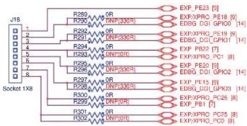
Figure 4-32. J18 Connector
text_image
J16 1 2 3 4 5 6 7 8 Socket 1X8 R289 OR R290 DNP(330R) R292 OR R291 DNP(390R) R294 OR R293 DNP(0R) R295 OR R296 DNP(330R) R297 OR R298 DNP(330R) R300 OR R299 DNP(0R) R301 OR R302 DNP(0R) EXP_PE23 [9] EXP/XPRO_PE18 [9] EDBG_DGI_GPIO [14] EXP/XPRO_PE19 [9] EDBG_DGI_GPIO1 [14] EXP_PB22 [7] EXP/XPRO_PC1 [8] EXP_PE20 [8] EDBG_DGI_GPIO2 [14] EXP_PE15 [8] EDBG_DGI_GPIO3 [14] EXP/XPRO_PC26 [8] EXP_PB1 [7] EXP/XPRO_PC25 [8] EXP/XPRO_PC0 [8]
natural_image
Close-up of a blue electronic circuit board with visible components and connectors (no readable text or symbols)Table 4-11. J18 Connector Signals
| Pin No. | SAMA5D44 PIO Muxing Alternates On-board Alternates | EDBG Alternate | |||||||
| 1 | PE23 | A25 | TCLK4 | MCI1_DA3 | - | - | - | ||
| 2 | PE18 | A18 | TIOA5 | MCI1_CK | - | - | - | - | DGI_GPIO0 |
| 3 | PE19 | A19 | TIOB5 | MCI1_CDA | - | - | - - | ||
| 4 | PB22 | SPI1_NPCS1 | D12 | - | PC1 | SPI0_MOSI | PWML2 | ISI_D9 | - |
| 5 | PE20 | A20 | TCLK5 | MCI1_DA0 | - | - | - | ||
| 6 | PE15 | A15 | SCK3 | TIOA0 | - | - | - | - | DGI_GPIO3 |
| 7 | PC26 | ISI_D7 | TWCK3 | UTXD1 | PB1 | G0_RXCK | SCK2 | ISI_PCK | - |
| 8 | PC25 | ISI_D6 | TWD3 | URXD1 | PC0 | SPI0_MISO | PWMH2 | ISI_D8 | - |
Figure 4-33. J19 Connector

text_image
J19 1 2 3 4 5 6 7 8 Socket 1X8 R304 OR R303 R305 OR R306 DNP(OR) EXP:XPRO_PE27 [9] EXP:XPRO_PE26 [9] EXP:XPRO_PD17 [9] EXP_PD18 [9] EXP:XPRO_PD13 [9] EXP_PD12 [9] EXP_TWDO_PA30 [7] EXP:XPRO_PC3 [8] EXP_TWCKO_PA31 [7] EXP:XPRO_PC2 [8]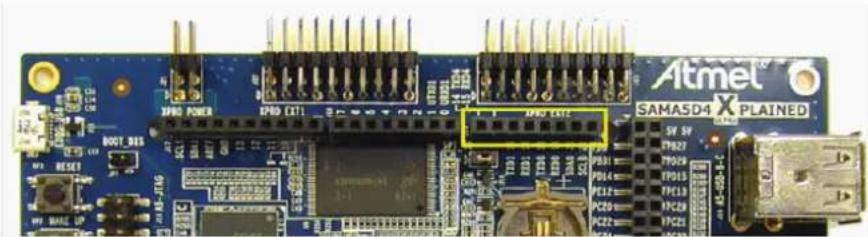
natural_image
Close-up of an Atmel SIMA5D4 X PLAINED microcontroller board with visible pin labels and connectors (no readable text beyond branding)Table 4-12. J19 Connector Signals
| Pin No. | SAMA5D44 PIO Muxing Alternates On-board Alternates | |||||||
| 1 | PE27 | NWR1/NBS1 | TXD4 | - | - | - | - | |
| 2 | PE26 | NCS2 | RXD4 | A18 | - | - | - | |
| 3 | PD17 | TXD1 | SPI2_NPCS0 | - | - | - | - | |
| 4 | PD16 | RXD1 | DCENB | - | - | - | ||
| 5 | PD13 | TXD0 | SPI2_MOSI | - | - | - | - | |
| 6 | PD12 | RXD0 | DCENA | - | - | - | ||
| 7 | PA30 | TWD0 | - | - | PC3 | SPI0_NPCS0 | PWML3 | ISI_D11 |
| 8 | PA31 | TWCK0 | - | - | PC2 | SPI0_SPCK | PWMH3 | ISI_D10 |
4.2.15.3 SAMA5D44 Peripheral Functions Available Through Arduino Headers
Table 4-13 provides details on access to the SAMA5D44 internal peripherals through the Arduino headers.
Note: Only one function at a time can be selected for each pin (refer to Section 4.3.15 in this document and the PIO controller section in SAMA5D4 Series datasheet).
Table 4-13. SAMA5D44 Peripheral Functions Available through the Arduino Headers
| Connector | SAMA5D44 to Arduino | System Function PCK ISI SSC SPI TWI | UART/USART ANALOG MISC | |||||||
| J14 | PB18 | - | - | - | - | SPI1_MISO | - | - | ||
| 3v3/5v | 3.3V/5V | - | - | - | - | - | - | - | - | |
| PB20 | - | - | - | - | SPI1_SPCK | - | - | - | - | |
| PB19 | - | - | - | - | SPI1_MOSI | - | - | |||
| nRST | nRST | - | - | - | - | - | - | - | - | |
| GND | GND | - | - | - | - | - | - | - | - | |
| J7 | PB28 | - | - | -TD0 | SPI2_NPCS3 | - | - | - | PWMH1 | |
| PC27 | - | - | - | SP40_NPCS2 | - | - | AD0 PWML0 | |||
| PC28 | - | - | - | SP40_NPCS3 | - | - | AD1 PWML1 | |||
| PC29 | - | - | - | - | - | -AD2 | PWMFI0 | |||
| PC30 | - | - | - | - | - | -AD3 PWMH0 | ||||
| PC31 | - | - | - | - | - | -AD4 PWMH1 | ||||
| PE24 | - | - | - | - | RTS3 | -- | - | - | ||
| PE5 | - | - | - | - | CTS3 | -- | - | - | ||
| J8 | PB30 | - | - | - | RF0 | - | TWCK2 | - | - | - |
| PB29 | - | - | - | RD0 | - | TWD2 | - | - | PWML1 | |
| PB26 | - | PCK0 | - | RK0 | - | - | - | - | PWMH0 | |
| PB10 | - | PCK2 | - | - | - | - | - | - | PWML1 | |
| PC0 | - | - | ISI_D8 | - | SPI0_MISO | - | - | - | PWMH2 | |
| PC1 | - | - | ISI_D9 | - | SPI0_MOSI | - | - | - | PWML2 | |
| PB14 | - | - | ISI_D10 | - | SPI0_SPCK | - | - | - | PWMH0 | |
| PB15 | - | - | - | - | - | - | - | - | PWML0 | |
| J17 | PE30 | - | - | ISI_HSYNC | - | - | TWCK1 | RXD2 | - | - |
| PE29 | - | - | ISI_VSYNC | - | - | TWD1 | CTS2 | - | - | |
| AREF | AREF | - | - | - | - | - | - | - | - | |
| GND | GND | - | - | - | - | - | - | - | - | |
| PB20 | - | - | - | - | SPI1_SPCK | - | - | - | TIOA3 | |
| PB18 | - | - | - | - | SPI1_MISO | - | - | - | TIOB3 | |
| PB19 | - | - | - | - | SPI1_MOSI | - | - | - | TCLK3 | |
| PB21 | - | - | - | - | SPI1_NPCS0 | - | - | - | - | |
| PE21 | - | - | - | - | - | - | - | - | TIOA4 | |
| PE22 | - | - | - | - | - | - | - | - | TIOB4 | |
| Connector | SAMA5D44 to Arduino | System Function | PCK | ISI | SSC | SPI | TWI | UART/USART | ANALOG | MISC |
| J18 | PE23 | - | - | - | - | - | - | - | - | |
| PE18 | - | - | - | - | - | - | - | - | ||
| PE19 | - | - | - | - | - | - | - | - | ||
| PB22 | - | - | ISI_D9 | - | SPI1_NPCS1 | - | - | - | ||
| PE20 | - | - | - | - | SPI2_NPCS1 | - | - | - | ||
| PE15 | - | - | - | - | SPI2_NPCS2 | - | - | - | ||
| PC26 | - | - | ISI_D8 | - | - | TWCK3 | UTXD1 | - | PWMH2 | |
| PC25 | - | - | ISI_PCK | - | - | TWD3 | URXD1 | - | - | |
| J19 | PE27 | - | - | - | - | - | - | TXD4 | - | - |
| PE26 | - | - | - | - | - | - | RXD4 | - | - | |
| PD17 | - | - | - | - | SPI2_NPCS0 | - | TXD1 | - | - | |
| PD16 | - | - | - | - | - | - | RXD1 | - | - | |
| PD13 | - | - | - | - | SPI2_MOSI | - | TXD0 | - | - | |
| PD12 | - | - | - | - | - | - | RXD0 | - | - | |
| PA30 | - | - | ISI_D11 | - | SPI0_NPCS0 | TWD0 | - | - | PWML3 | |
| PA31 | - | - | ISI_D10 | - | SPI0_SPCK | TWCK0 | - | - | PWMH3 | |
| J15 | 5V 5V - | - - - - - | ||||||||
| 5V 5V - | - - - - - | |||||||||
| PD8 - | PCK0/PCK1 | - | T | K | 0 | - | ||||
| PB27 | - | - | - | TF0 | SPI1_NPCS3 | - | - | - | PWML0 | |
| PB31 | - | - | - | - | - | - | - | - | - | |
| PD29 | - | - | - | - | - | SCK1 | - | - | ||
| PD14 | - | - | - | - | - | TWD0 | CTS1 | - | - | |
| PD15 | - | - | - | - | SPI2_SPCK | TWCK0 | RTS1 | - | - | |
| PE12 | - | - | - | - | - | - | - | - | PWMH2 | |
| PE13 - | - - - - - | - - - - - | PWML2 | |||||||
| PC20 | - | - | ISI_D1 | TF1 | - | - | - | - | - | |
| PC19 | - | - | ISI_D0 | TK1 | - | - | - | - | - | |
| PC22 | - | - | ISI_D3 | RF1 | - | - | - | - | - | |
| PC21 | - | - | ISI_D2 | TD1 | - | - | - | - | - | |
| PC24 | - | PCK1 | ISI_D5 | RK1 | - | - | - | - | - | |
| PC23 | - | - | ISI_D4 | RD1 | - | - | - | - | - | |
| PC26 | - | - | ISI_D7 | - | - | TWCK3 | UTXD1 | - | - | |
| PC25 | - | - | ISI_D6 | - | - | TWD3 | URXD1 | - | - | |
| PE25 | - | - | - | - | SPI0_MOSI | - | SCK4 | - | - | |
| PE0 | - | - | - | - | SPI0_MISO | - | CTS4 | - | - | |
| PE28 | - | - | - | - | SPI0_NPCS0 | - | RTS4 | - | - | |
| PB1 | - | - | - | - | SPI0_SPCK | - | SCK2 | - | - | |
| PD30 | - | - | - | - | - | - | - | - | ||
| PD31 | - | PCK1 | - | - | SPI0_NPCS2 | - | - | - | - | |
| PB3 - | - - - - - | CTS2 | - - | |||||||
| PB11 | - | - | - | - | - | - | RTS2 | - | PWMH1 | |
| PB4 | - | - | - | - | - | - | RXD2 | - | - | |
| PB5 | - | PCK2 | - | - | - - | TXD2 | - | - | ||
| PD28 | - | - | - | - | - | - | SCK0 | - | - | |
| PD11 | - | - | - | - | - | - | RTS0 | - | - | |
| PD10 - | - - - - - | CTS0 | - - | |||||||
| PD9 - | - - - - - | - - - - - | ||||||||
| PC3 | - | - | ISI_D11 | SPI0_NPCS0 | - | - | - | PWML3 | ||
| PE31 | - | - | - | - | - | - | - | - | ||
| GND | GND | - | - | - | - | - | - | - | - | |
| GND | GND | - | - | - | - | - | - | - | - | |
4.2.15.4 XPRO
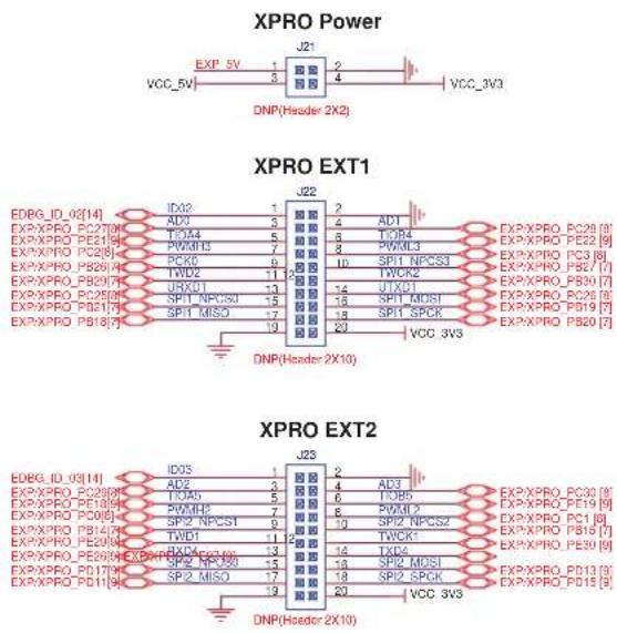
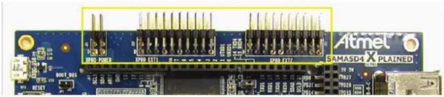
The SAMA5D4-XULT board embeds three connectors to interface Xplained PRO wings.
Figure 4-34. XPRO Connectors
text_image
XPRO Power EXP 5V 1 2 VCC_5V 3 4 DNP(Header 2X2) XPRO EXT1 ID02 1 2 AD0 3 4 AD1 TIOA4 5 6 TOR4 PWM13 7 8 PWM13 PCK0 9 10 SP11 NPCS1 TWD2 11 12 TWCK2 UPD0 13 14 UTX0 SP11 NPCS0 15 16 SP11 MDS1 SP11 MISO 17 18 SP11 SPCK DNP(Header 2X10) XPRO EXT2 ID03 1 2 AD2 3 4 AD3 TIOA5 5 6 TOB5 PWM3 7 8 PWM3 SP2 NPCS1 9 10 SP2 NPCS2 TWD1 11 12 TWCK UPD4 13 14 TXD4 SP2 NPCS0 15 16 SP2 MOSI SP2 MISO 17 18 SP2 SPCK DNP(Header 2X10)XPRO Connectors
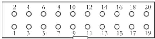
The standard extension headers include common signals. These are male 20-pin/100-mil/right-angled headers (extension boards feature a female 20-pin straight header).
Figure 4-35. XPRO Extension Headers
natural_image
Close-up of a blue electronic circuit board with multiple black connectors and labeled components (no readable text or symbols beyond labels)4.3 PIO Usage and Interface Connectors
4.3.1 Power Supply
Figure 4-36. Power Supply Connector J4

natural_image
Pure technical diagram of a mechanical component with concentric circles and a base, no text or symbols presentTable 4-14. Power Supply Connector J4 Signal Description
| Pin Mnemonic Signal Description | |
| 1 Center pin +5V | |
| 2 Spring blade GND | |
| 3 Fixing pin Floating |
4.3.2 JTAG/ICE Connector
Figure 4-37. JTAG J13
| Pin Mnemonic Signal Description | ||
| 1 VTref. | 3.3V power This is the target reference voltage (main 3.3V). | |
| 2 Vsupply. | 3.3V power | This pin is not connected in SAM-ICETM and reserved for compatibility with other equipment. Connected to main 3.3V. |
| 3 | nTRST TARGET RESET - Active-low output signal that resets the target | JTAG Reset. Output from SAM-ICE to control the Reset signal on the target system. |
| 4 GND | Common ground | |
| 5 | TDI TEST DATA INPUT - Serial data output line, sampled on the rising edge of the TCK signal | JTAG data input into target CPU |
| 6 GND | Common ground | |
| 7 TMS | TEST MODE SELECT JTAG mode set input into target CPU | |
| 8 GND | Common ground | |
| 9 | TCK TEST CLOCK - Output timing signal, for synchronizing test logic and control register access | JTAG clock signal into target CPU |
| 10 GND | Common ground | |
| 11 | RTCK - Input Return test clock signal from the target | Some targets having too slow system clock must synchronize the JTAG inputs to internal clocks. In present case such synchronization is unneeded and TCK merely looped back into RTCK. |
| 12 GND | Common ground | |
| 13 | TDO JTAG TEST DATA OUTPUT - Serial data input from the target | JTAG data output from target CPU |
| 14 GND | Common ground | |
| 15 nSRST | RESET Active-low reset signal. Target CPU reset signal. | |
| 16 GND | Common ground | |
| 17 RFU | This pin is not connected in SAM-ICE | |
| 18 GND | Common ground | |
| 19 RFU | This pin is not connected in SAM-ICE | |
| 20 GND | Common ground | |
4.3.3 EDBG USB Type Micro-AB
Figure 4-38. EDBG USB Type Micro-AB Connector J20
Table 4-16. EDBG USB Type Micro-AB Connector J20 Signal Descriptions
| Pin Mnemonic Signal Description | |
| 1 Vbus 5V power | |
| 2 DM Data minus | |
| 3 DP Data plus | |
| 4 ID On-the-go identification | |
| 5 GND Common ground |
4.3.4 USB Type A Dual Port
Figure 4-39. USB Type A Dual Port J16
natural_image
Line drawing of a multi-pin electrical connector with terminal blocks and leads (no text or symbols)Table 4-17. USB Type A Dual Port J16 Signal Descriptions
| Pin Mnem | onic Signal Description | |
| A1 Vbus - | USB_A 5V power | |
| A2 DM - | USB_A Data minus | |
| A3 DP - | USB_A Data plus | |
| A4 GND | Common ground | |
| B1 Vbus - | USB_A 5V power | |
| B2 DM - | USB_A Data minus | |
| B3 DP - | USB_A Data plus | |
| B4 GND | Common ground | |
| Mechanical pins | - | Shield |
4.3.5 USB Micro-AB
Figure 4-40. USB Host/Device Micro-AB Connector J11
Table 4-18. USB Host/Device Micro-AB Connector J11 Signal Descriptions
| Pin Mnemonic Signal Description | |
| 1 Vbus 5V power | |
| 2 DM Data minus | |
| 3 DP Data plus | |
| 4 ID On-the-go identification | |
| 5 GND Common ground |
4.3.6 DEBUG Connector
Figure 4-41. DEBUG Connector J1

Table 4-19. DEBUG Connector J1 Signal Descriptions
| Pin Mnemonic PIO Signal Description | |||
| 1 CTS3 | PE5 Handshake input | ||
| 2 TXD3 | (Transmitted Data) PE17 RS232 serial data input signal | ||
| 3 RXD3 | (Received Data) PE16 RS232 serial data output signal | ||
| 4 Power | - 5V/3.3V (selected by resistors) | ||
| 5 RTS3 | PE24 Handshake output | ||
| 6 GND | - Common ground | ||
4.3.7 SD/MMC Plus MCI0
Figure 4-42. SD/MMC Socket J24
natural_image
Isometric line drawing of a rectangular electronic component with mounting holes and slots (no text or symbols)Table 4-20. SD/MMC Socket J24 Signal Descriptions
| Pin Mnemonic PIO Signal Description | |||
| 1 DAT3 | PE23 Data Bit | ||
| 2 CMD | PE19 Command Line | ||
| 3 VSS – | Common ground | ||
| 4 VCC – | Supply Voltage 3.3V | ||
| 5 CLK | PE18 Clock / Command Line | ||
| 6 CD PE3 | Card Detect | ||
| 7 DAT0 | PE20 Data Bit | ||
| 8 DAT1 | PE21 Data Bit | ||
| 9 DAT2 | PE22 Data Bit | ||
| 10 | – | Not connected Data Bit | |
| 11 | – | Not connected Data Bit | |
| 12 | – | Not connected Data Bit | |
| 13 | – | Not connected Data Bit | |
| 14 | WP | GND | Write Protection (deactivated) |
| 15 | VSS – Common ground | ||
| 16 | VSS – Common ground | ||
4.3.8 MicroSD MCI1
Figure 4-43. MicroSD Socket J9

natural_image
Technical line drawing of a mechanical component with numbered parts (no text or symbols)Table 4-21. MicroSD Socket J9 Signal Descriptions
| Pin Mnemonic PIO Signal Description | |||
| 1 DAT2 PC8 Data Bit 2 | |||
| 2 CD/DA T3 PC9 Card Detect / Data Bit 3 | |||
| 3 CMD PC5 Command Line | |||
| 4 VCC – Supply Voltage 3.3V | |||
| 5 CLK | PC4 Clock / Command Line | ||
| 6 VSS | – Common ground | ||
| 7 DAT0 PC6 Data Bit 0 | |||
| 8 DAT1 PC7 Data Bit 1 | |||
| 9 CD PE2 Card Detect | |||
| 10 | GND | – Common ground | |
4.3.9 Ethernet ETH0 RJ45 Socket J12
Figure 4-44. Ethernet RJ45 Socket J12
12345678
RJ-45
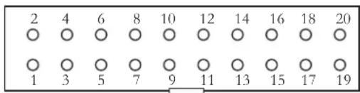
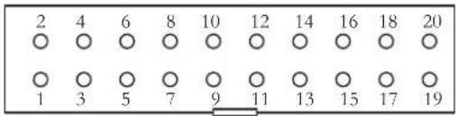
Figure 4-46. HDMI Type A Female Connector J5

Table 4-23. HDMI Type A Female Connector J5 Signal Descriptions
| Signal Pin No. Signal | |||
| TMDS Data 2+ 1 2 TMDS Data 2 Shield | |||
| TMDS Data 2- 3 4 TMDS Data 1+ | |||
| TMDS Data 1 Shield 5 6 TMDS Data 1- | |||
| TMDS Data 0+ 7 8 TMDS Data 0 Shield | |||
| TMDS Data 0- 9 10 TMDS Clock + | |||
| TMDS Clock Shield 11 12 TMDS Clock - | |||
| CEC (not connected) 13 14 Not connected | |||
| SCL 15 16 | SDA | ||
| GND | 17 18 | +5V | |
| Hot Plug Detect | 19 20 | DDC/CEC (GND) | |
4.3.12 XPRO Power Connector
Figure 4-47. XPRO Power Connector J21

Table 4-24. XPRO Power Connector J21 Signal Descriptions
| Signal Pin No. Signal | |||
| EXP_5V | 1 | 2 | |
| VCC_5V | 3 | 4 | VCC_3v3 |
4.3.13 XPRO Ext1 Connector
Figure 4-48. XPRO Ext1 Connector J22
Note: 1. Used by the EDBG interface.
4.3.14 XPRO Ext2 Connector
Figure 4-49. XPRO Ext2 Connector J23
Note: 1. Used by the EDBG interface.
4.3.15 PIO Usage
The following tables provide the use of different PIO lines on the SAMA5D4-XULT, sorted by PIO lines. Most of the signals can also be configured as either inputs or outputs from/to the processor.
Table 4-27. PIO A Pin Assignment and Signal Description
| Power Rail I/O | Type Primary Signal | Peripheral A Signal | Peripheral B Signal | Peripheral C Signal | |
| VDDIOP GPIO | PA0 LCDDAT0 - TMS | ||||
| VDDIOP GPIO | PA1 LCDDAT1 -- | ||||
| VDDIOP GPIO | CLK PA2 LCDDAT2 | G1_TXCK - | |||
| VDDIOP GPIO | CLK PA3 LCDDAT3 | G1_RXCK | - | ||
| VDDIOP GPIO | PA4 LCDDAT4 | G1_TXEN - | |||
| VDDIOP GPIO | PA5 LCDDAT5 | G1_TXER - | |||
| VDDIOP GPIO | PA6 LCDDAT6 | G1_CRS | - | ||
| VDDIOP GPIO | PA7 LCDDAT7 -- | ||||
| VDDIOP GPIO | PA8 LCDDAT8 - | TCK | |||
| VDDIOP GPIO | PA9 LCDDAT9 -- | ||||
| VDDIOP | GPIO | PA10 | LCDDAT10 | G1_RXDV | - |
| VDDIOP | GPIO | PA11 | LCDDAT11 | G1_RXER | - |
| VDDIOP GPIO | PA12 | LCDDAT12 G1_RX0 | - | ||
| VDDIOP GPIO | PA13 | LCDDAT13 G1_RX1 | - | ||
| VDDIOP GPIO | PA14 | LCDDAT14 G1_TX0 - | |||
| VDDIOP GPIO | PA15 | LCDDAT15 G1_TX1 - | |||
| VDDIOP | GPIO | PA16 | LCDDAT16 | - | NTRST |
| VDDIOP GPIO | PA17 | LCDDAT17 -- | |||
| VDDIOP GPIO | PA18 | LCDDAT18 G1_RX2 | - | ||
| VDDIOP GPIO | PA19 | LCDDAT19 G1_RX3 | - | ||
| VDDIOP GPIO | PA20 | LCDDAT20 G1_TX2 - | |||
| VDDIOP GPIO | PA21 | LCDDAT21 G1_TX3 - | |||
| VDDIOP | GPIO | PA22 | LCDDAT22 | G1_MDC | - |
| VDDIOP GPIO | PA23 | LCDDAT23 G1_MDIO - | |||
| VDDIOP | GPIO_CLK | PA24 | LCDPWM | PCK0 | - |
| VDDIOP GPIO | PA25 | LCDDISP TD0 | - | ||
| VDDIOP | GPIO | PA26 | LCDVSYNC | PWMH0 | SPI1_NPCS1 |
| VDDIOP | GPIO | PA27 | LCDHSYNC | PWML0 | SPI1_NPCS2 |
| VDDIOP | GPIO_CLK2 | PA28 | LCDPCK | PWMH1 | SPI1_NPCS3 |
| VDDIOP | GPIO | PA29 | LCDDEN | PWML1 | - |
| VDDIOP GPIO | PA30 | TWD0 | -- | ||
| VDDIOP GPIO | PA31 | TWCK0 | -- | ||
Table 4-28. PIO B Pin Assignment and Signal Description
| Power Rail I/O | Type Primary Signal | Peripheral A Signal | Peripheral B Signal | Peripheral C Signal | |
| VDDIOP GPIO | CLK PB0 G0_TXCK | -- | |||
| VDDIOP GPIO | CLK PB1 G0_RXCK | SCK2 ISI_PCK | |||
| VDDIOP GPIO | PB2 G0_TXEN | -- | |||
| VDDIOP GPIO | PB3 G0_TXER CTS2 | ISI_VSYNC | |||
| VDDIOP GPIO | PB4 | G0_CRS | RXD2 | ISI_HSYNC | |
| VDDIOP GPIO | PB5 | G0_COL_TXD2 | PCK2 | ||
| VDDIOP GPIO | PB6 G0_RXDV | -- | |||
| VDDIOP GPIO | PB7 G0_RXER | -- | |||
| VDDIOP GPIO | PB8 | G0_RX0 | -- | ||
| VDDIOP GPIO | PB9 | G0_RX1 | -- | ||
| VDDIOP GPIO | CLK | PB10 | G0_RX2 PCK2 | PWML1 | |
| VDDIOP | GPIO | PB11 | G0_RX3 | RTS2 | PWMH1 |
| VDDIOP GPIO | PB12 | G0_TX0 | -- | ||
| VDDIOP GPIO | PB13 | G0_TX1 | -- | ||
| VDDIOP | GPIO | PB14 | G0_TX2 | SPI2_NPCS1 | PWMH0 |
| VDDIOP | GPIO | PB15 | G0_TX3 | SPI2_NPCS2 | PWML0 |
| VDDIOP GPIO | PB16 | G0_MDC | -- | ||
| VDDIOP GPIO | PB17 | G0_MDIO | -- | ||
| VDDIOP GPIO | PB18 | SPI1_MISO D8 | - | ||
| VDDIOP GPIO | PB19 | SPI1_MOSI D9 | - | ||
| VDDIOP GPIO | CLK | PB20 | SPI1_SPCK D10 | - | |
| VDDIOP GPIO | PB21 | SPI1_NPCS0 D11 | - | ||
| VDDIOP | GPIO | PB22 | SPI1_NPCS1 | D12 | - |
| VDDIOP | GPIO | PB23 | SPI1_NPCS2 | D13 | - |
| VDDIOP | GPIO | PB24 | DRXD | D14 | TDI |
| VDDIOP | GPIO | PB25 | DTXD | D15 | TDO |
| VDDIOP | GPIO_CLK | PB26 | PCK0 | RK0 | PWMH0 |
| VDDIOP | GPIO | PB27 | SPI1_NPCS3 | TK0 | PWML0 |
| VDDIOP | GPIO | PB28 | SPI2_NPCS3 | TD0 | PWMH1 |
| VDDIOP | GPIO | PB29 | TWD2 | RD0 | PWML1 |
| VDDIOP | GPIO | PB30 | TWCK2 | RF0 | - |
| VDDIOP | GPIO | PB31 | - | TF0 | - |
Table 4-29. PIO C Pin Assignment and Signal Description
| Power Rail I/O | Type Primary Signal | Peripheral A Signal | Peripheral B Signal | Peripheral C Signal | |
| VDDIOM GPIO | PC0 SPI0_MISO PWMH2 ISI_D8 | ||||
| VDDIOM GPIO | PC1 SPI0_MOSI PWML2 ISI_D9 | ||||
| VDDIOM GPIO | CLK PC2 SPI0_SPCK PWMH3 ISI_D10 | ||||
| VDDIOM | GPIO | PC3 | SPI0_NPCS0 | PWML3 | ISI_D11 |
| VDDIOM | MCI_CLK | PC4 | SPI0_NPCS1 | MCI0_CK | PCK1 |
| VDDIOM GPIO | PC5 | D0 | MCI0_CDA | - | |
| VDDIOM GPIO | PC6 | D1 | MCI0_DA0 | - | |
| VDDIOM GPIO | PC7 | D2 | MCI0_DA1 | - | |
| VDDIOM GPIO | PC8 | D3 | MCI0_DA2 | - | |
| VDDIOM GPIO | PC9 | D4 | MCI0_DA3 | - | |
| VDDIOM | GPIO | PC10 | D5 | MCI0_DA4 | - |
| VDDIOM | GPIO | PC11 | D6 | MCI0_DA5 | - |
| VDDIOM | GPIO | PC12 | D7 | MCI0_DA6 | - |
| VDDIOM GPIO | PC13 | NRD/NANDOE | MCI0_DA7 | - | |
| VDDIOM | GPIO | PC14 | NWE/NANDWE | - | - |
| VDDIOM | GPIO | PC15 | NCS3 | - | - |
| VDDIOM GPIO | PC16 | NANDRDY | - | - | |
| VDDIOM GPIO | PC17 | A21/NANDALE - | - | ||
| VDDIOM GPIO | PC18 | A22/NANDCLE - | - | ||
| VDDIOM | GPIO | PC19 | ISI_D0 | TK1 | - |
| VDDIOM | GPIO | PC20 | ISI_D1 | TF1 | - |
| VDDIOM | GPIO | PC21 | ISI_D2 | TD1 | - |
| VDDIOM | GPIO | PC22 | ISI_D3 | RF1 | - |
| VDDIOM | GPIO | PC23 | ISI_D4 | RD1 | - |
| VDDIOM | GPIO | PC24 | ISI_D5 | RK1 | PCK1 |
| VDDIOM | GPIO | PC25 | ISI_D6 | TWD3 | URXD1 |
| VDDIOM GPIO | PC26 | ISI_D7 | TWCK3 UTXD1 | ||
| VDDANA | GPIO_ANA | PC27 | AD0 | SPI0_NPCS1 | PWML0 |
| VDDANA | GPIO_ANA | PC28 | AD1 | SPI0_NPCS2 | PWML1 |
| VDDANA | GPIO_ANA | PC29 | AD2 | SPI0_NPCS3 | PWMFI0 |
| VDDANA | GPIO_ANA | PC30 | AD3 | - | PWMH0 |
| VDDANA | GPIO_ANA | PC31 | AD4 | - | PWMH1 |
Table 4-30. PIO D Pin Assignment and Signal Description
| PIOD Mode Secure | Primary Signal | Peripheral A Signal | Peripheral B Signal | Peripheral C SignalPower | |
| VDDIOP GPIO | _CLK PD8 PCK0 -- | ||||
| VDDIOP GPIO | PD9 FIQ -- | ||||
| VDDIOP GPIO | PD10 CTS0 | CDETA | - | ||
| VDDIOP GPIO | PD11 | RTS0 SPI2_MISO | - | ||
| VDDIOP GPIO | PD12 | RXD0 DCENA | - | ||
| VDDIOP GPIO | PD13 TXD0 | SPI2_MOSI | - | ||
| VDDIOP GPIO | PD14 CTS1 | CDETB | - | ||
| VDDIOP GPIO | PD15 RTS1 | SPI2_SPCK | - | ||
| VDDIOP GPIO | PD16 | RXD1 DCENB | - | ||
| VDDIOP GPIO | PD17 TXD1 | SPI2_NPCS0 | - | ||
| VDDANA | GPIO_ANA | PD18 | - SENSE0 | - | |
| VDDANA | GPIO_ANA | PD19 | - SENSE1 | - | |
| VDDANA | GPIO_ANA | PD20 | - SENSE2 | - | |
| VDDANA | GPIO_ANA | PD21 | - SENSE3 | - | |
| VDDANA | GPIO_ANA | PD22 | - SENSE4 | - | |
| VDDANA | GPIO_ANA | PD23 | - SENSE5 | - | |
| VDDANA | GPIO_ANA | PD24 | - SENSE6 | - | |
| VDDANA | GPIO_ANA | PD25 | - SENSE7 | - | |
| VDDANA | GPIO_ANA | PD26 | - SENSE8 | - | |
| VDDANA | GPIO_ANA | PD27 | - SENSE9 | - | |
| VDDIOP GPIO | _CLK PD28 SCK0 -- | ||||
| VDDIOP GPIO | _CLK PD29 SCK1 DIS - | ||||
| VDDIOP GPIO | PD30 --- | ||||
| VDDIOP GPIO | _CLK PD31 SPI0_NPCS2 PCK1 - | ||||
Rail I/
Table 4-31. PIO E Pin Assignment and Signal Description
| Power Rail I/O | Type Primary Signal | Peripheral A Signal | Peripheral B Signal | Peripheral C Signal | |
| VDDIOM MCI_CLK PE0 A0/NBS0 MCI0_CDB CTS4 | |||||
| VDDIOM EBI PE1 A1 MCI0_DB0 - | |||||
| VDDIOM EBI PE2 A2 MCI0_DB1 - | |||||
| VDDIOM EBI PE3 A3 MCI0_DB2 - | |||||
| VDDIOM EBI PE4 A4 MCI0_DB3 - | |||||
| VDDIOM EBI PE5 A5 | CTS3 - | ||||
| VDDIOM EBI PE6 A6 | TIOA3 | - | |||
| VDDIOM EBI PE7 A7 | TIOB3 | PWMFI1 | |||
| VDDIOM EBI PE8 A8 | TCLK3 | PWML3 | |||
| VDDIOM EBI PE9 A9 | TIOA2 | - | |||
| VDDIOM | EBI | PE10 | A10 | TIOB2 | - |
| VDDIOM | EBI | PE11 | A11 | TCLK2 | - |
| VDDIOM | EBI | PE12 | A12 | TIOA1 | PWMH2 |
| VDDIOM | EBI | PE13 | A13 | TIOB1 | PWML2 |
| VDDIOM | EBI | PE14 | A14 | TCLK1 | PWMH3 |
| VDDIOM EBI | PE15 | A15 | SCK3 | TIOA0 | |
| VDDIOM EBI | PE16 | A16 | RXD3 | TIOB0 | |
| VDDIOM | EBI | PE17 | A17 | TXD3 | TCLK0 |
| VDDIOM | EBI | PE18 | A18 | TIOA5 | MCI1_CK |
| VDDIOM | EBI | PE19 | A19 | TIOB5 | MCI1_CDA |
| VDDIOM | EBI | PE20 | A20 | TCLK5 | MCI1_DA0 |
| VDDIOM | EBI | PE21 | A23 | TIOA4 | MCI1_DA1 |
| VDDIOM | EBI | PE22 | A24 | TIOB4 | MCI1_DA2 |
| VDDIOM | EBI | PE23 | A25 | TCLK4 | MCI1_DA3 |
| VDDIOM EBI | PE24 | NCS0 | RTS3 - | ||
| VDDIOM | EBI | PE25 | NCS1 | SCK4 | IRQ |
| VDDIOM | EBI | PE26 | NCS2 | RXD4 | A18 |
| VDDIOM EBI | PE27 | NWR1/NBS1 | TXD4 - | ||
| VDDIOM EBI | PE28 | NWAIT | RTS4 | A19 | |
| VDDIOP | DIB | PE29 | DIBP | URXD0 | TWD1 |
| VDDIOP | DIB | PE30 | DIBN | UTXD0 | TWCK1 |
| VDDIOP | GPIO | PE31 | ADTRG | - | - |
4.4 SAMA5D4-XULT Board Schematics
This section contains the following schematics:
- Block diagram
- PIO Muxing Table
Power Supply - SAMA5D44 - Power
- SAMA5D44 - DDR2
• SAMA5D44 - PIOA and PIOB
• SAMA5D44 - PIOC and Flash
• SAMA5D44 - SYS, PIOD, and PIOE
• JTAG, USB, DEBUG, and LCD
• HDMI - Ethernet_ETH0_10/100M
HSMCI
• EDBG
• Expansion and XPRO Connectors
Figure 4-50. Block diagram
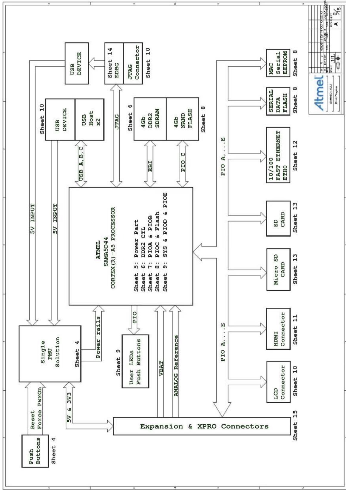
flowchart
graph TD
    A["Push Buttons"] -->|Reset Force PwrOn| B["Single PMU Solution"]
    B -->|5V & 3V3| C["Expansion & XPRO Connectors"]
    C -->|VBAT| D["Power rails"]
    C -->|ANALOG Reference| E["ATMEL SAMA5D44 CORTEX(R)-A5 PROCESSOR"]
    E -->|PIO| F["Micro SD CARD"]
    E -->|PIO C| G["SD CARD"]
    E -->|PIO A,...E| H["LCD Connector"]
    E -->|PIO A,...E| I["HDMI Connector"]
    E --> J["Micro SD CARD"]
    E --> K["SD CARD"]
    E --> L["10/100 FAST ETHERNET ETHO"]
    E --> M["SERIAL DATA FLASH"]
    E --> N["MAC Serial EEPROM"]
    B -->|5V INPUT| O["USB DEVICE"]
    B -->|5V INPUT| P["USB Host x2"]
    O --> Q["USB DEVICE"]
    P --> Q
    Q --> R["Sheet 14 EDBG"]
    Q --> S["JTAG Connector"]
    R --> T["Sheet 10"]
    S --> U["Sheet 10"]
    T --> V["USB Device"]
    U --> W["USB Device"]
    style A fill:#f9f,stroke:#333
    style B fill:#ccf,stroke:#333
    style C fill:#cfc,stroke:#333
    style D fill:#fcc,stroke:#333
    style E fill:#ffc,stroke:#333
    style F fill:#fcc,stroke:#333
    style G fill:#fcc,stroke:#333
    style H fill:#fcc,stroke:#333
    style I fill:#fcc,stroke:#333
    style J fill:#fcc,stroke:#333
    style K fill:#fcc,stroke:#333
    style L fill:#fcc,stroke:#333
    style M fill:#fcc,stroke:#333
    style N fill:#fcc,stroke:#333
Figure 4-51. PIO Muxing Table
PIO Muxing & Jumper setting
| PIOA | USAGE | PIOA | USAGE | USAGE | USAGE | USAGE | PIOC | INDEXID/BPIOB | |||
| PA0 | LCDDAT0/JTAG_TMS | PA16 | LCDDAT16/NTRST | PB0 | GO_TXCK | PB16 | GO_MDC | PC0 | SPI0_MISO/PWMH2/ISI_D8 | PC16 | NAND_RDY |
| PA1 | LCDDAT1 | PA17 | LCDDAT17 | PB1 | SCK2/ISI_PCK | PB17 | GO_MDIO | PC1 | SPI0_MOSI/PWML2/ISI_D9 | PC17 | NAND_ALE |
| PA2 | LCDDAT2 | PA18 | LCDDAT18 | PB2 | GO_TXEN | PB18 | SPI1_MISO | PC2 | SPI0_SPCK/PWMH3/ISI_D10 | PC18 | NAND_CLE |
| PA3 | LCDDAT3 | PA19 | LCDDAT19 | PB3 | CTS2/ISI_VSYNC | PB19 | SPI1_MOSI | PC3 | SPI0_NPCS0/PWML3/ISI_D11 | PC19 | ISI_D0/TK1 |
| PA4 | LCDDAT4 | PA20 | LCDDAT20 | PB4 | RXD2/ISI_HSYNC | PB20 | SPI1_SPCK | PC4 | MCI0_CK/PCK1 | PC20 | ISI_D1/TF1 |
| PA5 | LCDDAT5 | PA21 | LCDDAT21 | PB5 | TXD2/PCK2 | PB21 | SPI1_NPCS0 | PC5 | MCI0_CDA/NAND_D0 | PC21 | ISI_D2/TD1 |
| PA6 | LCDDAT6 | PA22 | LCDDAT22 | PB6 | GO_RXDV | PB22 | SPI1_NPCS1 | PC6 | MCI0_DA0/NAND_D1 | PC22 | ISI_D3/RF1 |
| PA7 | LCDDAT7 | PA23 | LCDDAT23 | PB7 | GO_RXER | PB23 | SPI1_NPCS2 | PC7 | MCI0_DA1/NAND_D2 | PC23 | ISI_D4/RD1 |
| PA8 | LCDDAT8/JTAG_TCK | PA24 | LCDPWM/HDMI_MCK | PB8 | GO_RXO | PB24 | JTAG_TDI | PC8 | MCI0_DA2/NAND_D3 | PC24 | ISI_D5/RK1/PCK1 |
| PA9 | LCDDAT9 | PA25 | LCDDISP/HDMI_INT | PB9 | GO_RX1 | PB25 | JTAG_TDO | PC9 | MCI0_DA3/NAND_D4 | PC25 | ISI_D6/TWD3/URXD1 |
| PA10 | LCDDAT10 | PA26 | LCDVSYNC | PB10 | PCK2/PWML1 | PB26 | PCK0/RK0/PWMH0 | PC10 | NAND_D5 | PC26 | ISI_D7/TWCK3/UTXD1 |
| PA11 | LCDDAT11 | PA27 | LCDHSYNC | PB11 | RTS2/PWMH1 | PB27 | SPI1_NPCS3/HDMI_TKO/PWML0 | PC11 | NAND_D6 | PC27 | AD0_XP/PWMLO |
| PA12 | LCDDAT12 | PA28 | LCDPCK | PB12 | GO_TXO | PB28 | SPI2_NPCS3/HDMI_TDO/PWMH1 | PC12 | NAND_D7 | PC28 | AD1_XM/PWML1 |
| PA13 | LCDDAT13 | PA29 | LCDDEN | PB13 | GO_TX1 | PB29 | TWD2/RDO/PWML1 | PC13 | NAND_RE | PC29 | AD2_YP/PWMH0 |
| PA14 | LCDDAT14 | PA30 | TWDC | PB14 | SPI2_NPCS1/PWMH0 | PB30 | TWCK2/RF0 | PC14 | NWE/NAND_WE | PC30 | AD3_YM/PWMH0 |
| PA15 | LCDDAT15 | PA31 | TWCK0 | PB15 | SPI2_NPCS2/PWMLO/HDMI_RST | PB31 | HDMI_TFO | PC15 | NAND_NCS3 | PC31 | AD4/PWMH1 |
| PIOD | PIOD | EGASU | EGASU | EGASU | PIOE | IOE | EGASU | ||
| PD16 | RXD1 | PE0 | USB_OVCUR/CTS4 | PE16 | DBGU_RXD3 | ||||
| PD17 | TXD1/SPI2_NPCS0 | PE1 | GO_IRQ | PE17 | DBGU_TXD3 | ||||
| PD18 | SENSE0 | PE2 | MCI0_CD | PE18 | TIOA5/MCI1_CK | ||||
| PD19 | SENSE1 | PE3 | MCI1_CD | PE19 | TIOB5/MCI1_CDA | ||||
| PD20 | SENSE2 | PE4 | MCI1_PWR | PE20 | TCLK5/MCI1_DA0 | ||||
| PD21 | SENSE3 | PE5 | DBGU_CTS3 | PE21 | TIOA4/MCI1_DA1 | ||||
| PD22 | SENSE4 | PE6 | TIOA3 | PE22 | TIOB4/MCI1_DA2 | ||||
| PD23 | SENSE5 | PE7 | TIOB3 | PE23 | TCLK4/MCI1_DA3 | ||||
| PD8 | PCK0 | PD24 | SENSE6 | PE8 | PB_USER/TCLK3 | PE24 | DBGU_RTS3 | ||
| PD9 | FIQ | PD25 | SENSE7 | PE9 | LCD_IRQ1 | PE25 | PMIC_IRQ/SCK4 | ||
| PD10 | CTSO | PD26 | SENSE8 | PE10 | LCD_IRQ2 | PE26 | RXD4 | ||
| PD11 | RTS0/SPI2_MISO | PD27 | SENSE9 | PE11 | USB8_EN5V | PE27 | TXD4 | ||
| PD12 | RXD0 | PD28 | SCK0 | PE12 | TIOA1/PWMR2 | PE28 | RTS4 | ||
| PD13 | TXDO/SPI2_MOSI | PD29 | SCK1 | PE13 | TIOB1/PWML2 | PE29 | URXD0/TWD1 | ||
| PD14 | CTS1 | PD30 | LED_POWER | PE14 | USBC_EN5V | PE30 | UTXD0/TWCK1 | ||
| PD15 | RTS1/SPI2_SPCK | PD31 | SPI0_NPCS2/PCK1 | PE15 | LED_USER/LCD_ID/TIOA0 | PE31 | USBA_VBUS | ||
| JUMPER DESCRIPTION | ||
| PART | DEFAULT | FUNCTION |
| JP1 | OPEN | Disable EDBG |
| JP2 | SHORT | I VCC 3V3 Measurement |
| JP3 | SHORT | I_1V2 HDMI Measurement |
| JP4 | SHORT | I VDDIODDR MPU Measurement |
| JP5 | SHORT | I VDDCORE Measurement |
| JP6 | SHORT | I_VDDBU Measurement |
| JP7 | OPEN | Disable CS SPI&Nand Flash Memory |
| JP8 | DNP | CS SPI Flash Memory |
| LCD | |
| ID_SYS | 1 |
| GND | 2 |
| LCDDAT0 | 3 |
| LCDDAT1 | 4 |
| LCDDAT2 | 5 |
| LCDDAT3 | 6 |
| GND | 7 |
| LCDDAT4 | 8 |
| LCDDAT5 | 9 |
| LCDDAT6 | 10 |
| LCDDAT7 | 11 |
| GND | 12 |
| LCDDAT8 | 13 |
| LCDDAT9 | 14 |
| LCDDAT10 | 15 |
| LCDDAT11 | 16 |
| GND | 17 |
| LCDDAT12 | 18 |
| LCDDAT13 | 19 |
| LCDDAT14 | 20 |
| LCDDAT15 | 21 |
| GND | 22 |
| LCDDAT16 | 23 |
| LCDDAT17 | 24 |
| LCDDAT18 | 25 |
| LCDDAT19 | 26 |
| GND | 27 |
| LCDDAT20 | 28 |
| LCDDAT21 | 29 |
| LCDDAT22 | 30 |
| LCDDAT23 | 31 |
| GND | 32 |
| LCDPCK | 33 |
| LCDVSYNC | 34 |
| LCDHSYNC | 35 |
| LCDDEN | 36 |
| SPI1_SPCK/AD3_YM | 37 |
| SPI1_MOSI/AD2_YP | 38 |
| SPI1_MISO/AD1_XM | 39 |
| SPI1_NPCS2/AD0_XP | 40 |
| LCDDISP | 41 |
| TWDO | 42 |
| TWCK0 | 43 |
| IRQ1 | 44 |
| IRQ2 | 45 |
| LCDPWM | 46 |
| Reset | 47 |
| VCC | 48 |
| VCC | 49 |
| GND | 50 |
| A | B | C | D | E | F |
| A | INIT EDIT | 29 Aug 14 | XX XX XX | ||
| NO. | POS. | DATE | VER. | ||
| SAMSDA-XULT | SCALE: 1/1 | FELV. SHEET | |||
| PIO Mining | A 3/15 | ||||
Figure 4-52. Power Supply

text_image
EDBG USB VBUS SVD4 R426 BR USS_VOUTS_SVD R426 BR EXP_SVD5 J5 DIN/DC Jok 5V/2A Input R401 DNIPOR R406 DNIPOR EXP_VATREF BAT1 Battery Holder 3V C84 100kF VCC_3V D11 BAT3C VDDL 3V U1S VIN VOUT CL GND CDS 100kF NCP469209Q20T1G C19 1uF C176 4.7uF C175 4.7uF C14 4.7uF C176 4.7uF C176 4.7uF VCC_3V VCC_3V VCC_3V VCC_3V VCC_3V VCC_3V VCC_3V VCC_3V VCC_3V VCC_3V VCC_3V VCC_3V VCC_3V VCC_3V VCC_3V VCC_3V VCC_3V VCC 2V R161 4.7K R187 68K R188 110K 1% RESET VCC_3V8 RNST 3V8MFS 5V8I0 RNST 2V8[8] R161 4.7K R187 68K R188 110K 1% ADC10000000000000000000000000000000000000000000000000000000000000000000000000000000000000000000000000000 U2 ACTB8XQ385 T C194 C190 INL45 INL27 L3 2.2uF C27 2.2uF C28 2.2uF C29 2.2uF C25 2.2uF C24 2.2uF C21 2.2uF C1 2.2uF C3 2.2uF C2 2.2uF C1 2.2uF C2 2.2uF C1 2.2uF C2 2.2uF C1 2.2uF C2 2.2uF C1 2.2uF C2 2.2uF C1 2.2uF C2 2.2uF C1 2.2uF C2-1 1.6 uF C3 1.6 uF C4 1.6 uF C5 1.6 uF C6 1.6 uF C7 1.6 uF C8 1.6 uF C9 1.6 uF C10 1.6 uF C11 1.6 uF C12 1.6 uF C13 1.6 uF C14 1.6 uF C15 1.6 uF C16 1.6 uF C17 1.6 uF C18 1.6 uF C19 1.6 uF C20 1.6 uF C21 1.6 uF C22 1.6 uF C23 1.6 uF C24 1.6 uF C25 1.6 uF C26 1.6 uF C27 1.6 uF C28 1.6 uF C29 1.6 uF C3 1.6 uF C31 1.6 uF C32 1.6 uF C33 1.6 uF C34 1.6 uF C35 1.6 uF C36 1.6 uF C37 1.6 uF C38 1.6 uF C39 1.6 uF C4 1.6 uF C41 1.6 uF C42 1.6 uF C43 1.6 uF C44 1.6 uF C45 1.6 uF C46 1.6 uF C47 1.6 uF C48 1.6 uF C49 1.6 uF C5 1.6 uF C51 1.6 uF C52 1.6 uF C53 1.6 uF C54 1.6 uF C55 1.6 uF C56 1.6 uF C57 1.6 uF C58 1.6 uF C59 1.6 uF C6 1.6 uF C61 1.6 uF C62 1.6 uF C63 1.6 uF C64 1.6 uF C65 1.6 uF C66 1.6 uF C67 1.6 uF C68 1.6 uF C69 1.6 uF C7 1.6 uF C71 1.6 uF C72 1.6 uF C73 1.6 uF C74 1.6 uF C75 1.6 uF C76 1.6 uF C77 1.6 uF C78 1.6 uF C79 1.6 uFFigure 4-53. SAMA5D44 - Power
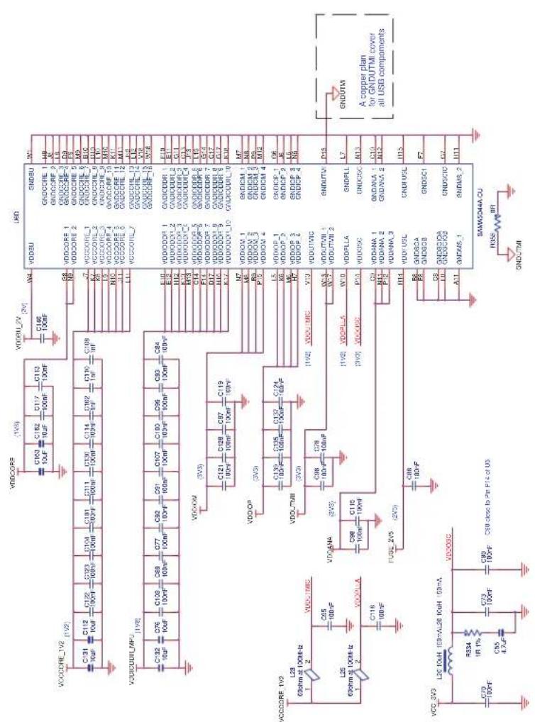
text_image
VDDCORE (C13) C14 C15 C16 C17 C18 C19 C20 C21 C22 C23 C24 C25 C26 C27 C28 C29 C30 C31 C32 C33 C34 C35 C36 C37 C38 C39 C40 C41 C42 C43 C44 C45 C46 C47 C48 C49 C50 C51 C52 C53 C54 C55 C56 C57 C58 C59 C60 C61 C62 C63 C64 C65 C66 C67 C68 C69 C70 C71 C72 C73 C74 C75 C76 C77 C78 C79 C80 C81 C82 C83 C84 VDDCORE_1/VS VDDCORE_2/VS VDDCORE_3/VS VDDCORE_4/VS VDDCORE_5/VS VDDCORE_6/VS VDDCORE_7/VS VDDIDOUT_1/GNDBU GNDCCRE 1/NB GNDCCRE 2/LB GNDCCRE 3/D9 GNDCCRE 4/M9 GNDCCRE 5/BIO GNDCCRE 6/C10 GNDCCRE 7/LT0 GNDCCRE 8/M10 GNDCCRE 9/K11 GNDCCRE 10/M12 GNDCCRE 11/M13 GNDCCRE 12/L14 GNDCCRE 13/L15 GNDCCRE 14/V8 GNDCCRE 15/M9-8 VDDODOUT_1/GNDCCRE 1/L19 GNDCCRE 1/GNDCCRE 2/GNDCCRE 3/GNDCCRE 4/GNDCCRE 5/GNDCCRE 6/GNDCCRE 7/GNDCCRE 8/GNDCCRE 9/GNDCCRE 10/GNDCCRE 11/GNDCCRE 12/GNDCCRE 13/GNDCCRE 14/GNDCCRE 15/GNDCCRE 16/ VDDODOUT_1/GNDCCRE 1/GNDCCRE 2/GNDCCRE 3/GNDCCRE 4/GNDCCRE 5/GNDCCRE 6/GNDCCRE 7/GNDCCRE 8/GNDCCRE 9/GNDCCRE 10/GNDCCRE 11/GNDCCRE 12/GNDCCRE 13/GNDCCRE 14/GNDCCRE 15/GNDCCREPOWER TEST POINTS

text_image
VCC_5V TP1 SMDTPI1 SMDC_3V3 TP12 SMDTPI2SMDRU_2V1 TP16 SMDTPI2SMD 19V VCCORE_1V2 FUSE_2V5 VCC_1D0G VOJ76 VOJ77 TP8 SMDTPI4 SMD TP8 SMDTPI5 SMD TP8 SMDTPI6 SMD TP8 SMDTPI7 SMD TP8 SMDTPI8 SMD TP8 SMDTPI9 SMD TP8 SMDTPI10 SMD TP8 SMDTPI11 SMD TP8 SMDTPI12 SMD TP8 SMDTPI13 SMD TP8 SMDTPI14 SMD TP8 SMDTPI15 SMD TP8 SMDTPI16 SMD TP8 SMDTPI17 SMD TP8 SMDTPI18 SMD TP8 SMDTPI19 SMD TP8 SMDTPI20 SMD TP8 SMDTPI21 SMD TP8 SMDTPI22 SMD TP8 SMDTPI23 SMD TP8 SMDTPI24 SMD TP8 SMDTPI25 SMD TP8 SMDTPI26 SMD TP8 SMDTPI27 SMD TP8 SMDTPI28 SMD TP8 SMDTPI29 SMD TP8 SMDTPI30 SMD TP8 SMDTPI31 SMD TP8 SMDTPI32 SMD TP8 SMDTPI33 SMD TP8 SMDTPI34 SMDtext_image
MCU_DDR VOCICDDR L17 10uF 130mA/L17 10uH 100mA C158 4.7uF R331 1R 1%) C62 4.3uF C60 10uF C2K 1% R29 10uF C2K 1% DOR_VREF VOCICDDR C143 2.2uF C51 100-F C75 10uF C56 10uF C79 10uF C120 10uF C72 10uF C142 10uF C155 10uF C59 10uF C74 10uF C57 10uF C149 10uF C148 10uF C149 10uF C58 10uF C28 2.2uF C33 2.2uF C133 100-F C124 10uF C146 10uF C62 10uF C129 10uF C71 10uF C59 10uF C130 10uF C68 2.2uF C33 2.2uF SALMS36A-CCU USB DOR A0 DOR A1 DOR A2 DOR A3 DOR A4 DOR A5 DOR A6 DOR A7 DOR A8 DOR A9 DOR A10 DOR A11 DOR A12 DOR A13 DOR A14 DOR CLK DOR CLKN DOR CKE DOR CSB DOR CSB+ 2.2k 1% DOR CA5 DOR CA6 DOR WE DOR BNG DOR BA1 DOR BA2 DOR BA3- DDR DCSO 2.2k 1% DDR CALN 2.2k 1% DDR CALP 2.2k 1% DDR VREF 2.2k 1% DDR VREF 2.2k 1% DDR CLKN 2.2k 1% DDR CLKN 2.2k 1% DDR CLKN 2.2k 1% DDR CLKN 2.2k 1% DDR CLKN 2.2k 1% DDR CLKN 2.2k 1% DDR CLKN 2.2k 1% DDR CLKN 2.2k 1% DDR CLKN 2.7k 1% DDR CLKN 2.7k 1% DDR CLKN 2.7k 1% DDR CLKN 2.7k 1% DDR CLKN 2.7k 1% DDR CLKN 2.7k 1% DDR CLKN 2.7k 1% DDR CLKN 2.7k 1% DDR CLKN 2.7k 1% DDR CLKN 2.7k 1% DDR CLKN 2.7k 1% DDR CLKN 2.7k 1% DDR CLKN 2.7k 1% DDR CLKN 2.7k 1% DDR CLKN 2.7k 1% DDR CLKN 2.7k 1% DDR CLKN 2.7k 1% DDR CLKN-2.7k 1% DDR CLKN-2.7k 1% DDR CLKN-2.7k 1% DDR CLKN-2.7k 1% DDR CLKN-2.7k 1% DDR CLKN-2.7k 1% DDR CLKN-2.7k 1% DDR CLKN-2.7k 1% DDR CLKN-2.7l 1% DDR CLKN-2.7l 1% DDR CLKN-2.7l 1% DDR CLKN-2.7l 1% DDR CLKN-2.7l 1% DDR CLKN-2.7l 1% DDR CLKN-2.7l 1% DDR CLKN-2.7l 1% DDR CLKN-2.7l 1% DDR DCR R330 DDR DCR R330 DDR DCR R330 DDR DCR R330 DDR DCR R330 DDR DCR R330 DDR DCR R330 DDR DCR R330 DDR DCR R330 DDR DCR R330 DDR DCR R330 DDR DCR R330 DCR DCR R330 DCR DCR R330 DCR DCR R330 DCR DCR R330 DCR DCR R330 DCR DCR R330 DCR DCR R330 DCR DCR R330 DCR DCR R330 DCR DCR R330 DCR DCR R330 DCRC DCR R330 DCRC DCR R330 DCRC DCR R330 DCRC DCR R330 DCRC DCR R330 DCRC DCR R330 DCRC DCR R330 DCRC DCR R330 DCRC DCR R330 DCRC DCR R330 DCRC DCR R330 DCRC VREF VOCICDDR L7: 10uF - 150mA/LT: 5xH - 50mA VOCICDDR L7: 10uF - 150mA/LT: 5xH - 50mA VOCICDDR L7: 10uF - 150mA/LT: 5xH - 50mA VOCICDDR L7: 10uF - 150mA/LT: 5xH - 50mA VOCICDDR L6: - - - - - - - - - - - - - - - - - - - - - - - - - - - - - - - - - - - - - - - - - - - - - - - - - - - - - - - - - - - - - - - - - - - - - - - - - - - - - - - - - - - - - - - - - - - - - - - - - - VOCICDDR L6: - - - - - - - - - - - - - - - - - - - - - - - - - - - - - - - - - - - - - - - - - - - - - - - - - - - - - - - - VOCICDDR L6: + - VOCICDDR L6: + - VOCICDDR L6: + - VOCICDDR L6: + - VOCICDDR L6: + - VOCICDDR L6: + - VOCICDDR L6: + - VOCICDDR L6: + - VOCICDDR L6: + - VOCICDDR L6: + - VOCICDDR L6: + - VOCICDDR L6: +- VOCICDDR L6: + - VOCICDDR L6: + - VOCICDDR L6: + - VOCICDDR L6: + - VOCICDDR L6: + - VOCICDDR L6: + - VOCICDDR L6: + - VOCICDDR L6: + - VOCICDDR L6: + - VOCICDDR L6: + - VOCICDDR L6: + - MTCCHI2MHRT-SEC C DDR2 Hold notes as sheet or possible, therefore, DDRS traces have to be padable cross, as possible of SALMS44 The input FDI DDR2 should not be rated in impedance traces of ZoL, such as standard capacitance. Address, control and data traces may not exceed 18 inches (≥6 mm) Address, control and data traces must be length matched to within <4 inch (≥54 mm). Address, control and data traces must match the class group trace lengths to within ≥8 inches (≤85mm). Address, control and data traces must match the class group trace lengths to within ≥8 inches (≤85mm). Address, control and data traces must match the class group trace lengths to within ≥8 inches (≤85mm). Address, control and data traces must match the class group trace lengths to within ≥8 inches (≤85mm). Address, control and data traces must match the class group trace lengths to within ≥8 inches (≤85mm). Address, controller and data traces must match the class group trace lengths to within ≥8 inches (≤85mm). Address, controller and data traces must match the class group trace lengths to within ≥8 inches (≤85mm). Address, controller and data traces must match the class group trace lengths to within ≥8 inches (≤85mm). Address, controller and data traces must match the class group trace lengths to within ≥8 inches (≤85mm). Address, controller and data traces should match the class group trace lengths to within ≥8 inches (≤85mm). Address, controller and data traces should match the class group trace lengths to within ≥8 inches (≤85mm). Address, controller and data traces should match the class group trace lengths to within ≥8 inches (≤85mm). Address, controller and data traces should match the class group trace lengths to within ≥8 inches (≤85mm). Address, controller and data traces should match the class groups trace lengths to within ≥8 inches (≤85mm). Address, controller and data traces should match the class groups trace lengths to within ≥8 inches (≤85mm). Address, controller and data traces should match the class groups trace lengths to within ≥8 inches (≤85mm). Address, controller and data traces should match the class groups trace lengths to within ≥8 inches (≤85mm). Address, controller and data traces should match the class groups trace lengths to inside ≥8 inches (≤85mm). Address, controller and data traces should match the class groups trace lengths to inside ≥8 inches (≤85mm). Address, controller and data traces should match the class groups trace lengths to inside ≥8 inches (≤85mm). Address, controller and data traces should match the class groups trace lengths to inside ≥8 inches (≤85mm). Address, controller and data traces should match the class groups trace lengths to inside ≥8 inches (<6 mm) Address, controller and data traces should match the class groups trace lengths to inside ≥8 inches (<6 mm) Address, controller and data traces should match the class groups trace lengths to inside ≥8 inches (<6 mm) Address, controller and data traces should match the class groups trace lengths to inside ≥8 inches (<6 mm) Address, controller and data traces should match the class groups trace lengths to inside ≥8 inches (<6 mm) Address, controller and data traces should match the class groupstrace lengths to inside ≥8 inches (<6 mm) Address, controller and data traces should match the class groupstrace lengths to inside ≥8 inches (<6 mm) Address, controller and data traces should match the class groupstrace lengths to inside ≥8 inches (<6 mm) Address, controller and data traces should match the class groupstrace lengths to inside ≥8 inches (<6 mm) Address, controller and data traces should match the class groupstrace lengths to inside ≥8 inches (<6 mm) Address, controller I/O/II/O/III/O/IV/O/VI/O/VO/O/VI/O/VO/O/VI/O/VI/O/VI/O/VI/O/VI/O/VI/O/VI/O/VI/O/VI/O/VI/O/VI/O/VI/O/VI/O/VI/O/VI/O/VI/O/VI/O/VI/O/VI/O/VI/O/VI/O/VI/O/VI/O/VI/O/VI/O/VI/O/VI/O/VI/O/VI/O/VI/O/VI/O/VI/O/VI/O/VI_O/ Atmel® A B C N E M T O X P Q X X X X X X X X X X X X X X X X X X X X X X X X X X X X X X X X X X X X X X X X X X X X X X X X X X X X X X X X X X X X X X X X X X X X X X X X X X X X X X X X X X X X X X X X X X X X X X X X X X X XX YX YX YX YX YX YX YX YX YX YX YX YX YX YX YX YX YX YX YX YX YX YX YX YX YX YX YX YX YX YX YX YX YX YX YX YX YX YX YX YX YX YX YX YX YX YX YX YX YX YXYQYQYQYQYQYQYQYQYQYQYQYQYQYQYQYQYQYQYQYQYQYQYQYQYQYQYQYQYQYQYQYQYQYQYQYQYQYQYQYQYQYQYQYQYQYQYQYQYQYQYQA B C N E M T O X P Q X X X X X X X X X X X X X X X X X X X X X X X X X X X X X X X X X X X X X X X X X X X X X X X X X X X X X XFigure 4-55. SAMA5D44 - PIOA and PIOB

other
PIOA USE PAXLCDNAT181 PAXLCDNAT191 PAXLCDNAT181 PAXLCDNAT191 PAXLCDNAT181 PAXLCDNAT191 PAXLCDNAT181 PAXLCDNAT191 PAXLCDNAT181 PAXLCDNAT191 PAXLCDNAT181 PAXLCDNAT190 PAXLCDNAT181 PAXLCDNAT190 PAXLCDNAT181 PAXLCDNAT190 PAXLCDNAT181 PAXLCDNAT190 PAXLCDNAT181 PAXLCDNAT190 PAXLCDNAT181 PAXLCDNAT191 PAXLCDNAT181 PAXLCDNAT190 PAXLCDNAT181 PAXLCDNAT190 PAXLCDNAT181 PAXLCDNAT190 PAXLCDNAT181 PAXLCDNAT191 PAXLCDNAT181 PAXLCDNAT191 PAXLCDNAT181 PAXLCDNAT190 PAXLCDNAT181 PAXLCDNAT190 PAXLCDNAT181 PAXLCDNAT191 PAXLCDNAT181 PAXLCDNAT190 PAXLCDNAT181 PAXLCDNAT191 PAXLCDNAT181 PAXLCDNAT190 PAXLCDNAT181 PAXLCDNAT190 PAXLCDNAT181 PAXLCDNAT191 PAXLCDNAT181 PAXLCDNAT192 PAXLCDNAT181 PAXLCDNAT192 PAXLCDNAT182 PAXLCDNAT192 PAXLCDNAT182 PAXLCDNAT192 PAXLCDNAT182 PAXLCDNAT192 PAXLCDNAT182 PAXLCDNAT192 PAXLCDNAT182 PAXLCDNAT192 PAXLCDNAT183 PAXLCDNAT192 PAXLCDNAT183 PAXLCDNAT192 PAXLCDNAT183 PAXLCDNAT192 PAXLCDNAT183 PAXLCDNAT192 PAXLCDNAT183 PAXLCDNAT192 PAXLCDNAT184 PAXLCDNAT192 PAXLCDNAT184 PAXLCDNAT192 PAXLCDNAT184 PAXLCDNAT192 PAXLCDNAT184 PAXLCDNAT192 PAXLCDNAT184 PAXLCDNAT 75/75/75/75/75/75/75/75/75/75/75/75/75/75/75/75/75/75/75/75/75/75/75/75/75/75/75/75/75/75/75/75/75/75/Figure 4-56. SAMA5D44 - PIOC and Flash
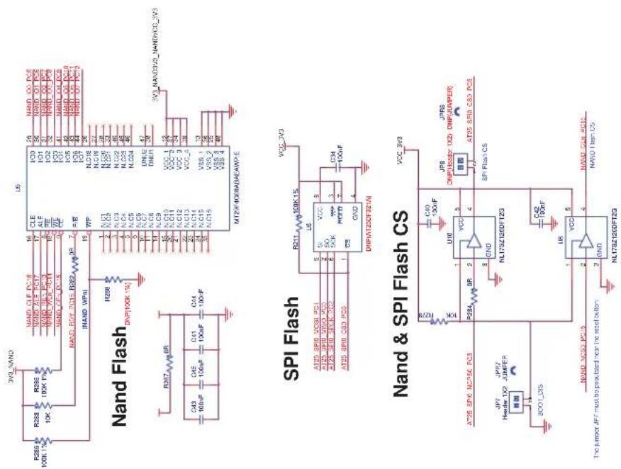
text_image
Nand Flash R286 100K 1% R288 10K R286 100K 1% NAND CLE PC-16 NAND ALF PC17 NAND PD18 PC19 NAND VCC PC20 NAND CE21 PC22 NAND RDY PC23 R282 INAND WPN IN258 DNP(100K 1%) R267 8R C43 100uF C46 100uF C41 100uF C44 100uF L12VIF400A0BAEAWP-E L12VIF400A0BAEAWP-E L12VIF400A0BAEAWP-E L12VIF400A0BAEAWP-E L12VIF400A0BAEAWP-E L12VIF400A0BAEAWP-E L12VIF400A0BAEAWP-E L13VCC 3V3_NAND3V3_NANDVCC_3V3 AT25 SPB VCBI PC1 AT25 SPB VIVO PC2 AT25 SPB SPRK PC3 AT25 SPB CAB PCS SPI Flash AT25 SPK NCPSX PC3 JP7 Header 1X2 JPM7 JUMPER JCOM1_CIS NAND VCCS PC15 The jumper JP7 must be proutted near the reset button NAND SBN PC15 NAND I fan CS| A | B | 3 | 4(Mx) | 11 Oct. 14 | XX XX |
| A | INT EDT | 29 Aug. 14 | XX XX XXX | ||
| RPA | DATE | ORDER | SALADOM | ||
| SAMS04-XULT | SCALE: 1/1 | FELV. SHEET | |||
| SAMS04- PDC & FLASH | 8/15 | ||||
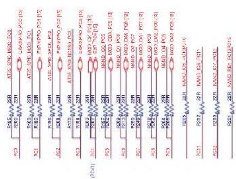
text_image
PC01 R155 2R AT3S SP6 MDS PC8 PC01 R161 2R AT3S SP6 MDS PC1 PC01 R169 2R AT3S SP6 MDS PC1 PC01 R170 2R ATPN/POI PC1 PC02 R186 2R AT3S SP6 SPECT PC8 PC02 R191 2R ATPN/POI PC1 PC02 R179 2R AT3S NOD NOSP0 PC8 PC03 R181 2R ATPN/POI PC8 PC03 R183 3H NOD OK PC4 [13] PC03 R187 3H EXP PC4 [13] PC05 R187 2R NAND OC PC8 PC05 R189 2R NAND OJ1 PC8 PC05 R191 2R NAND DAG PC8 [13] PC05 R200 2R NAND OS PC7 PC05 R209 2R NAND OJ4 PC8 PC05 R278 2R NAND OJ4 PC8 PC05 R274 2R NAND DAZ PC8 [13] PC05 R294 2R NAND OJ4 PC8 PC05 R295 2R NAND DAZ PC8 [13] PC05 R295 2R NAND DAZ PC8 PC05 R295 2R NAND DAZ PC8 PC05 R295 2R NAND DAZ PC8 PC05 R295 2R NAND DAZ PC8 PC05 R295 2R NAND DAZ PC8 PC05 R295 2R NAND DAZ PC8 PC05 R295 2R NAND DAZ PC8 PC05 P212 2R NAND DAZ PC8 PC05 P213 2R NAND DAZ PC8 PC05 P214 2R NAND DAZ PC8 PC05 P215 2R NAND DAZ PC8 PC05 P216 2R NAND DAZ PC8 PC05 P217 2R NAND DAZ PC8 PC05 P218 2R NAND DAZ PC8 PC05 P219 2R NAND DAZ PC8 PC05 P220 2R NAND DAZ PC8 PC05 P221 2R NAND DAZ PC8 PC05 P222 2R NAND DAZ PC8 PC05 P223 2R NAND DAZ PC8 PC05 P224 2R NAND DAZ PC8 PC05 P225 2R NAND DAZ PC8 PC05 P226 2R NAND DAZ PC8 PC05 P227 2R NAND DAZ PC8 PC05 P228 2R NAND DAZ PC8 PC05 P229 2R NAND DAZ PC8 PC05 P230 2R NAND DAZ PC8 PC05 P231 2R NAND DAZ PC8 PC05 P232 2R NAND DAZ PC8 PC05 P233 2R NAND DAZ PC8 PC05 P234 2R NAND DAZ PC8 PC05 P235 2R NAND DAZ PC8 PC05 P236 2R NAND DAZ PC8 PC05 P237 2R NAND DAZ PC8 PC05 P238 2R NAND DAZ PC8 PC05 P239 2R NAND DAZ PC8 PC05 P240 2R NAND DAZ PC8 PC05 P241 2R NAND DAZ PC8 PC05 P242 2R NAND DAZ PC8 PC05 P243 2R NAND DAZ PC8 PC05 P244 2R NAND DAZ PC8 PC05 P245 2R NAND DAZ PC8 PC05 P246 2R NAND DAZ PC8 PC05 P247 2R NAND DAZ PC8 PC05 P248 2R NAND DAZ PC8 PC05 P249 2R NAND DAZ PC8 PC05 P250 2R NAND DAZ PC8 PC05 P251 2R NAND DAZ PC8 PC05 P252 2R NAND DAZ PC8 PC05 P253 2R NAND DAZ PC8 PC05 P254 2R NAND DAZ PC8 PC05 P255 2R NAND DAZ PC8 PC05 P256 2R NAND DAZ PC8 PC05 P257 2R NAND DAZ PC8 PC05 P258 2R NAND DAZ PC8 PC05 P259 2R NAND DAZ PC8 PC05 P260 2R NAND DAZ PC8 PC05 P261 2R NAND DAZ PC8 PC05 P262 2R NAND DAZ PC8 PC05 P263 2R NAND DAZ PC8 PC05 P264 2R NAND DAZ PC8 PC05 P265 2R NAND DAZ PC8 PC05 P266 2R NAND DAZ PC8 PC05 P267 2R NAND DAZ PC8 PC05 P268 2R NAND DAZ PC8 PC05 P269 2R NAND DAZ PC8 PC05 P270 2R NAND DAZ PC8 PC05 P271 2R NAND DAZ PC8 PC05 P272 2R NAND DAZ PC8 PC05 P273 2R NAND DAZ PC8 PC05 P274 2R NAND DAZ PC8 PC05 P275 2R NAND DAZ PC8 PC05 P276 2R NAND DAZ PC8 PC05 P277 2R NAND DAZ PC8 PC05 P278 2R NAND DAZ PC8 PC05 P279 2R NAND DAZ PC8 PC05 P280 2R NAND DAZ PC8 PC05 P281 2R NAND DAZ PC8 PC05 P282 2R NAND DAZ PC8 PC05 P283 2R NAND DAZ PC8 PC05 P284 2R NAND DAZ PC8 PC05 P285 2R NAND DAZ PC8 PC05 P286 2R NAND DAZ PC8 PC05 P287 2R NAND DAZ PC8 PC05 P288 2R NAND DAZ PC8 PC05 P289 2R NAND DAZ PC8 PC05 P290 2R NAND DAZ PC8 PC05 P291 2R NAND DAZ PC8 PC05 P292 2R NAND DAZ PC8 PC05 P311 3M NOSP-DCP-DCP-DCP-DCP-DCP-DCP-DCP-DCP-DCP-DCP-DCP-DCP-DCP-DCP-DCP-DCP-DCP-DCP-DCP-DCP-DCP-DCP-DCP-DCP-DCP-DCP-DCP-DCP-DCP-DCP-DCP-DCP-DCP-DCp-DCP-DCP-DCP-DCP-DCP-DCP-DCP-DCP-DCP-DCP-DCP-DCP-DCP-DCP-DCP-DCP-DCP-DCP-DCP-DCP-DCP-DCP-DCP-DCP-DCP-DCP-DCP-DCP-DCP-DCP-DCP-DCP-DCP
text_image
TWI3 VCC 20A R255 R262 R271 2.2K 1% PC25 R255 R262 R271 R258 R262 R271 PC25 R271 R262 R277 R262 R271 R276 R262 R271 PAC_TW3A_PC25 [1] EXPXPO_PC25 [1] PAC_LW3A_PC25 [1] EXPXPO_PC25 [1] PAC_XP_PC27 [10] LWXP0.PC27 [10] AD1_XV_PC28 [10] LWXP0.PC28 [10] PAC_YV_PC29 [10] EXPXPO_PC29 [10] PAC_ZV_PC30 [10] LWXP0.PC30 [10] AD1_YV_PC31 [10] EXPXPO_PC31 [10]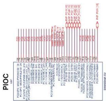
text_image
PICC USF PCOSPEC MISO/PWMH201 D8 Y6 PCC PCOSPEC MOSI/PWMH201 D8 Y5 PCC PCOSPEC SPCK/PWMH1_D10 Y2 PCC PCOSPEC NPSO/PWMH30_D11 Y0 PCC PCOSPEC NPSO/SPCK/MSCD40 Y7 PCC PCOSPEC NPSO/SPCK/D40 Y8 PCC PCOSPEC NPSO/SPCK/D40 Y9 PCC PCOSPEC NPSO/SPCK/D40 Y10 PCC PCOSPEC NPSO/SPCK/D40 Y11 PCC PCOSPEC NPSO/SPCK/D40 Y12 PCC PCOSPEC NPSO/SPCK/D40 Y13 PCC PCOSPEC NPSO/SPCK/D40 Y14 PCC PCOSPEC NPSO/SPCK/D40 Y15 PCC PCOSPEC NPSO/SPCK/D40 Y16 PCC PCOSPEC NPSO/SPCK/D40 Y17 PCC PCOSPEC NPSO/SPCK/D40 Y18 PCC PCOSPEC NPSO/SPCK/D40 Y19 PCC PCOSPEC NPSO/SPCK/D40 Y20 PCC PCOSPEC NPSO/SPCK/D40 Y21 PCC PCOSPEC NPSO/SPCK/D40 Y22 PCC PCOSPEC NPSO/SPCK/D40 Y23 PCC PCOSPEC NPSO/SPCK/D40 Y24 PCC PCOSPEC NPSO/SPCK/D40 Y25 PCC PCOSPEC NPSO/SPCK/D40 Y26 PCC PCOSPEC NPSO/SPCK/D40 Y27 PCC PCOSPEC NPSO/SPCK/D40 Y28 PCC PCOSPEC NPSO/SPCK/D40 Y29 PCC PCOSPEC NPSO/SPCK/D40 Y30 PCC PCOSPEC NPSO/SPCK/D40 Y31 PCC PCOSPEC NPSO/SPCK/D40 Y32 PCC PCOSPEC NPSO/SPCK/D40 Y33 PCC PCOSPEC NPSO/SPCK/D40 Y34 PCC PCOSPEC NPSO/SPCK/D40 Y35 PCC PCOSPEC NPSO/SPCK/D40 Y36 PCC PCOSPEC NPSO/SPCK/D40 Y37 PCC PCOSPEC NPSO/SPCK/D40 Y38 PCC PCOSPEC NPSO/SPCK/D40 Y39 PCC PCOSPEC NPSO/SPCK/D40 Y40 PCC PCOSPEC NPSO/SPCK/D40 Y41 PCC PCOSPEC NPSO/SPCK/D40 Y42 PCC PCOSPEC NPSO/SPCK/D40 Y43 PCC PCOSPEC NPSO/SPCK/D40 Y44 PCC PCOSPEC NPSO/SPCK/D40 Y45 PCC PCOSPEC NPSO/SPCK/D40 Y46 PCC PCOSPEC NPSO/SPCK/D40 Y47 PCC PCOSPEC NPSO/SPCK/D40 Y48 PCC PCOSPEC NPSO/SPCK/D40 Y49 PCC PCOSPEC NPSO/SPCK/D40 Y50 PCC PCOSPEC NPSO/SPCK/D40 Y51 PCC PCOSPEC NPSO/SPCK/D40 Y52 PCC PCOSPEC NPSO/SPCK/D40 Y53 PCC PCOSPEC NPSO/SPCK/D40 Y54 PCC PCOSPEC NPSO/SPCK/D40 Y55 PCC PCOSPEC NPSO/SPCK/D40 Y56 PCC PCOSPEC NPSO/SPCK/D40 Y57 PCC PCOSPEC NPSO/SPCK/D40 Y58 PCC PCOSPEC NPSO/SPCK/D40 Y59 PCC PCOSPEC NPSO/SPCK/D40 Y60 PCC PCOSPEC NPSO/SPCK/D40 Y61 PCC PCOSPEC NPSO/SPCK/D40 Y62 PCC PCOSPEC NPSO/SPCK/D40 Y63 PCC PCOSPEC NPSO/SPCK/D40 Y64 PCC PCOSPEC NPSO/SPCK/D40 Y65 PCC PCOSPEC NPSO/SPCK/D40 Y66 PCC PCOSPEC NPSO/SPCK/D40 Y67 PCC PCOSPEC NPSO/SPCK/D40 Y68 PCC PCOSPEC NPSO/SPCK/D40 Y69 PCC PCOSPEC NPSO/SPCK/D40 Y70 PCC PCOSPEC NPSO/SPCK/D40 Y71 PCC PCOSPEC NPSO/SPCK/D40 Y72 PCC PCOSPEC NPSO/SPCK/D40 Y73 PCC PCOSPEC NPSO/SPCK/D40 Y74 PCC PCOSPEC NPSO/SPCK/D40 Y75 PCC PCOSPEC NPSO/SPCK/D40 Y76 PCC PCOSPEC NPSO/SPCK/D40 Y77 PCC PCOSPEC NPSO/SPCK/D40 Y78 PCC PCOSPEC NPSO/SPCK/D40 Y79 PCC PCOSPEC NPSO/SPCK/D40 Y80 PCC PCOSPEC NPSO/SPCK/D40 Y81 PCC PCOSPEC NPSO/SPCK/D40 Y82 PCC PCOSPEC NPSO/SPCK/D40 Y83 PCC PCOSPEC NPSO/SPCK/D40 Y84 PCC PCOSPEC NPSO/SPCK/D40 Y85 PCC PCOSPEC NPSO/SPCK/D40 Y86 PCC PCOSPEC NPSO/SPCK/D40 Y87 PCC PCOSPEC NPSO/SPCK/D40 Y88 PCC PCOSPEC NPSO/SPCK/D40 Y89 PCC PCOSPEC NPSO/SPCK/D40 Y90 PCC PCOSPEC NPSO/SPCK/D40 Y91 PCC PCOSPEC NPSO/SPCK/D40 Y92 PCC PCOSPEC NPSO/SPCK/D40 Y93 PCC PCOSPEC NPSO/SPCK/D40 Y94 PCC PCOSPEC NPSO/SPCK/D40 Y95 PCC PCOSPEC NPSO/SPCK/D40 Y96 PCC PCOSPEC NPSO/SPCK/D40 Y97 PCC PCOSPEC NPSO/SPCK/D40 Y98 PCC PCOSPEC NPSO/SPCK/D40 Y99 PCC PCOSPEC NPSO/SPCK/D40 Y100 | EXP PCS1 [18] EXP PCS2 [19] EXP PCS3 [19] EXP PCS4 [19] EXP PCS5 [19] EXP PCS6 [19] EXP PCS7 [19] EXP PCS8 [19] EXP PCS9 [19] EXP PCS10 [19] EXP PCS11 [19] EXP PCS12 [19] EXP PCS13 [19] EXP PCS14 [19] EXP PCS15 [19] EXP PCS16 [19] EXP PCS17 [19] EXP PCS18 [19] EXP PCS19 [19] EXP PCS20 [19] EXP PCS21 [19] EXP PCS22 [19] EXP PCS23 [19] EXP PCS24 [19] EXP PCS25 [19] EXP PCS26 [19] EXP PCS27 [19] EXP PCS28 [19] EXP PCS29 [19] EXP PCS30 [19] EXP PCS31 [19] EXP PCS32 [19] EXP PCS33 [19] EXP PCS34 [19] EXP PCS35 [19] EXP PCS36 [19] EXP PCS37 [19] EXP PCS38 [19] EXP PCS39 [19] EXP PCS40 [19] EXP PCS41 [19]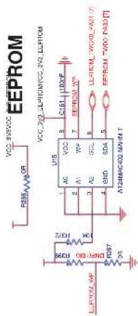
text_image
EEPROM VCC_3V0_2LDPROM/VCC_3V0_2LFPROM VCC_3V0_2LDPROM/VCC_3V0_2LFPROM A1 2 VCC 8 C150 100F A1 4 WZ 7 EEPROM WP A2 3 SCL 8 LFPROM _WDO_PAST(7) A2 4 END 6DA 5 EEPROM _TWO_PAST(7) A124MMC402 MNVATFigure 4-57. SAMA5D44 - SYS, PIOD, and PIOE
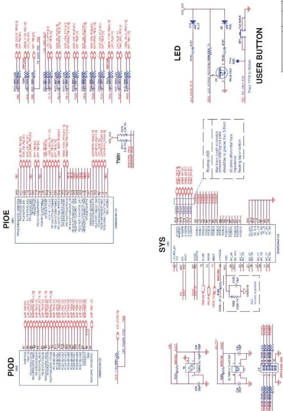
| A | B | C | D | E | F |
| A | B/F | E/F | 11-Oct-14 | XXX | XX |
| REV. | 29-Aug-14 | REV. | DATE:XXX | ||
| SAMS04-XULT | |||||
| SAMS04-SYS & PIOD & PIOD | SCALE: 1/1 | REV. | SHEET: A 9/15 | ||
Figure 4-58. JTAG, USB, DEBUG, and LCD

text_image
LCD VCC_SV VCC_9V3 R416 R417 R53 R53 R53 R53 R53 R53 R53 R53 R53 R53 R53 R53 R53 R53 R53 R53 R53 R53 R53 R53 R53 R53 R53 R53 R53 R52 R52 R52 R52 R52 R52 R52 R52 R52 R52 R52 R52 R52 R52 R52 R52 R52 R52 R52 R52 R52 R52 R52 R52 R52 R51 R51 R51 R51 R51 R51 R51 R51 R51 R51 R51 R51 R51 R51 R51 R51 R51 R51 R51 R51 R51 R51 R51 R51 R51 R50 R49 R48 R47 R46 R45 R44 R43 R42 R41 R40 R39 R38 R37 R36 R35 R34 R33 R32 R31 R30 R29 R28 R27 R26 R25 R24 R23 R22 R21 R20 R19 R18 R17 R16 R15 R14 R13 R12 R11 R10 R9 R8 R7 R6 R5 R4 DISP_PA26 LCCDAI700P0000000000000000000000000000000000000000000000000000000000000000000000000000000000000000000000000000- LCD_PAM_PA24 LCD_VCL9PAAQ4PAAQ4PAAQ4PAAQ4PAAQ4PAAQ4PAAQ4PAAQ4PAAQ4PAAQ4PAAQ4PAAQ4PAAQ4PAAQ4PAAQ4PAAQ4PAAQ4PAAQ4PAAQ4PAAQ4PAAQ4PAAQ4PAAQ4PAAQ4PAAQ4PAAQ8-7-7-7-7-7-7-7-7-7-7-7-7-7-7-7-7-7-7-7-7-7-7-7-7-7-7-7-7-7-7-7-7-7-7-7-7-7-7-7-7-7-7-7-7-7-7- LCD_PAM_PA24 (LDCAI7) (LDCAI7) (LDCAI7) (LDCAI7) (LDCAI7) (LDCAI7) (LDCAI7) (LDCAI7) (LDCAI7) (LDCAI7) (LDCAI7) (LDCAI7) (LDCAI7) (LDCAI7) (LDCAI7) (LDCAI7) (LDCAI7) (LDCAIC) LCD_PAM_PA24 (LDCAI7) (LDCAI7) (LDCAI7) (LDCAI7) (LDCAI7) (LDCAI7) (LDCAI7) (LDCAI7) (LDCAI7) (LDCAI7) (LDCAI7) (LDCAI7) (LDCAI7) (LDCAI7) (LDCAI7) (LDCCN) LCD_PAM_PA24 (LDCAI7) (LDCAI7) (LDCAI7) (LDCAI7) (LDCAI7) (LDCAI7) (LDCAI7) (LDCAI7) (LDCAI7) (LDCAI7) (LDCAI7) (LDCAI7) (LDCAI7) (LDCAI7) (LDCAI7) LCD_PAM_PA24 (LDCAI7) (LDCAI7) (LDCAI7) (LDCAI7) (LDCAI7) (LDCAI7) (LDCAI7) (LDCAI7) (LDCAI7) (LDCAI7) (LDCAI7) (LDCAI7) (LDCAIC) LCD_PAM_PA24 (LDCAI7) (LDCAI7) (LDCAiT) LCD_PAM_PA24 (LDCAiT) (LDCAiT) (LDCAiT) (LDCAiT) (LDCAiT) (LDCAiT) (LDCAiT) (LDCAiT) (LDCAiT) (LDCAiT) LCD_PAM_PA24 (LDCAiT) (LDCAiT) (LDCAiT) (LDCAiT) (LDCAiT) (LDCAiT) (LDCAiT) (LDCAiT) LCD_PAM_PA24 (LDCAiT) (LDCAiT) (LDCAiT) (LDCAiT) (LDCAiT) (LDCAiT) (LDCAiT) LCD_PAM_PA24 (LDCAiT) (LDCAiT) (LDCAiT) (LDCAiT) (LDCAiT) (LDCAiT) LCD_PAM_PA24 (LDCAiT) (LDCAiT) (LDCAiT) (LDCAiT) (LDCAiT) (LDCAiT) LCD_PAM_PA24 (LDCAiT) (LDCAiT) (LCCDAI) LCD_PAM_PA24 (LCCDAI) LCD_PAM_PA24 (LCCDAI) LCD_PAM_PA24 (LCCDAI) LCD_PAM_PA24 (LCCDAI) LCD_PAM_PA24 (LCCDAI) LCD_PAM_PA24 (LCCDAI) LCD_PAM_PA24 (LCCDAI) LCD_PAM_PA24 (LCCDAI) LCD_PALPCBPLCPLCPLCPLCPLCPLCPLCPLCPLCPLCPLCPLCPLCPLCPLCPLCPLCPLCPLCPLCPLCPLCPLCPLCPLCPLCPLCPLCPLCPLCPLCPLCPLCPLCPLCPLCPLCPLCPLCPLCPLCPLCPLCPLCPLCPLCPLCPLCPLCPLCPLSPLCPLCPLCPLCPLCPLCPLCPLCPLCPLCPLCPLCPLCPLCPLCPLCPLCPLCPLCPLCPLCPLCPLCPLCPLCPLCPLCPLCPLCPLCPLCPLCPLCPLCPLCPLCPLCPLCPLCPLCPLCPLCPLCPLCPLCPLCPLCPLCPLCPLCSLPCLPCLPCLPCLPCLPCLPCLPCLPCLPCLPCLPCLPCLPCLPCLPCLPCLPCLPCLPCLPCLPCLPCLPCLPCLPCLPCLPCLPCLPCLPCLPCLPCLPCLPCLPCLPCLPCLPCLPCLPCLPCLPCLPCLPCLPCLPCLPCLPCLPCLRC LCCDAIP C PCLC PCL C PCLC PCL C PCLC PCL C PCLC PCL C PCLC PCL C PCLC PCL C PCLC PCL C PCLC PCL C PCLC PCL C PCLC PCL C PCLC PCL C PCLC PCL C PCLC PCL C PCLC PCL C PCLC PCL C PCLC PCL C PCLC PCL C PCLC PCL C PCLC PCL C PCLC PCL C PCLC PRL C PCLC PRL C PCLC PRL C PCLC PRL C PCLC PRL C PCLC PRL C PCLC PRL C PCLC PRL C PCLC PRL C PCLC PRL C PCLC PRL C PCLC PRL C PCLC PRL C PCLC PRL C PCLC PRL C PCLC PRL C PCLC PRL C PCLC PRL C PCLC PRL C PCLC PRL C PCLC PBL C PCLC PBL C PCLC PBL C PCLC PBL C PCLC PBL C PCLC PBL C PCLC PBL C PCLC PBL C PCLC PBL C PCLC PBL C PCLC PBL C PCLC PBL C PCLC PBL C PCLC PBL C PCLC PBL C PCLC PBL C PCLC PBL C PCLC PBL C PCLC PBL C PCLC PBL C PCLC PBl C PCLC PBL C PCLC PBL C PCLC PBL C PCLC PBL C PCLC PBL C PCLC PBL C PCLC PBL C PCLC PBL C PCLC PBL C PCLC PBL C PCLC PBL C PCLC PBL C PCLC PBL C PCLC PBL C PCLC PBL C PCLC PBL C PCLC PBL C PCLC PBL C PCLC PBL C PCLC PRL C PCLC PRL C PCLC PRL C PCLC PRL C PCLC PRL C PCLC PRL C PCLC PRL C PCLC PRL C PCLC PRL C PCLC PRL C PCLC PRL C PCLC PRL C PCLC PRL C PCLC PRL C PCLC PRL C PCLC PRL C PCLC PRL C PCLC PRL C PCLC PRL C PCUC D PVC PCM CPU PCM CPU PCM CPU PCM CPU PCM CPU PCM CPU PCM CPU PCM CPU PCM CPU PCM CPU PCM CPU PCM CPU PCM CPU PCM CPU PCM CPU PCM CPU PCM CPU PCM CPU PCM CPU PCM CPU PCM CPU PCM CPU PCM CPU PCM CPU PCM CPU PCM CPU PCM CPU PCM CPU PCM CPU PCM CPU PCM CPU PCM CPU PCM CPU PCM CPU PCM CPU PCM CPU PCM CPU PCM CPU PCM CPU PCM CPU PCM CPU PCM CPU PCM CPU PCM CPU PCM CPU PCM CPU PCM CPU PCM CPU PCM CPU PCM CPU PCM PVH 8.8.8.8.8.8.8.8.8.8.8.8.8.8.8.8.8.8.8.8.8.8.8.8.8.8.8.8.8.8.8.8.8.8.8.8.8.8.8.8.8.8.8.8.8.8.8.8.8.8.8 8.8.8.8.8.8.8.8.8.8.8.8.8.8.8.8.8.8.8.8.8.8.8.8.8.8.8.8 8 8 8 8 8 8 8 8 8 8 8 8 8 8 8 8 8 8 8 8 8 8 8 8 8 8 8 8 8 8 8 8 8 8 8 8 8 8 8 8 8 8 8 8 8 8 8 8 8 8

text_image
DEBUG DDR1_CTS1_PES0 DDR1_XDS_PH70_R1 DDR1_RXD_PB10_R1 DDR1_HSS_PZ40 R11 R12 R13 R14 R15 R16 R17 R18 R19 R20 R21 R22 R23 R24 R25 R26 R27 R28 R29 R30 R31 R32 R33 R34 R35 R36 R37 R38 Fheader 1X8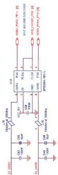
text_image
5V USRS C63 100nF C65 10uF L18 190ohm at 100kHz VCC 5V C68 100nF C7 1 2 L16 1900hm at 100kHz U12 CUTA EVA 1 IN FLEA 2 ONQ FLOB 3 OUTB EVB 4 SP2256A-1EN-L USB, ENV, NE14 [I] ENA and ENB Active High USB_ONCURPEN [II] USB_ENSV_P511 [III]
text_image
JTAG VCC_5V3 R224 100K 1% F222 100K 1% F227 100K 1% R217 100K 1% R220 3R NTRS [1] TCK [7,14] LMS [7,5] TCK [7,14] TDC [7,4] NRST 3V3 [4,12-4,15] Headar ZX10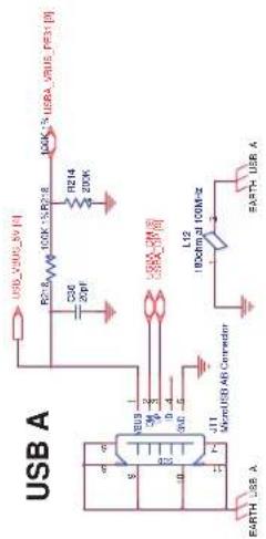
text_image
USB A USB_VIRUS_SV [R218 100K 15R218 100K 15 USRA_VIRUS_FR31 [R214 20kF] C36 20pF R214 20kF J11 MicroUSB AB Connector L12 180cm at 100M-cc EARTH_USB_A EARTH_USB_AUSB B & C

text_image
J7 USB A Upper J15 USB Connector J7 USB B Lower USB DM USB DP 5 6 7 8 9 10 11 12 EARTH_USB_B/C L15 180GHz at 100MHz 1 2 EARTH_USB_B/C| A | RevA | XinJG | 11 Oct. 14 | XXX | XX XX XX |
| A | INT CRT | XinJG | 29-Aug-14 | XXX | XX XX XX |
| BRA | W/INT | TXG | LANT | OFF | DATE |
| SCALE: 1/1 | REV.A | SHEET10/15 | |||
Figure 4-59. HDMI

text_image
HDMI Type A Connector J5 HDMI 132 3 CAT2 70V 2.4V MT10 -CM1 SC1 15 ACI MT19 MT10 MT12 MT13 MT12 MT10 MT10 MT10 MT10 MT10 MT10 MT10 MT10 MT10 MT10 MT10 MT10 MT10 MT10 MT10 MT10 MT10 MT10 MT10 MT10 MT10 MT10 MT10 MT10 MT10 MT15 -CM1 TOG 5 W/WR 70V 2.4V CAT2 S 6 ATG 70V 2.4V CAT2 S 6 ATG 70V 2.4V CAT2 S 6 ATG 70V 2.4V CAT2 S 6 ATG 70V 2.4V CAT2 S 6 ATG 70V 2.4V CAT2 S 6 ATG 70V 2.4VFigure 4-60. Ethernet_ETH0_10/100M

text_image
100 ohms differential trace impedance Routing top or bottom J12 RJ45 Connector TX TX TX TX TX TX TX TX TX TX TX TX TX TX TX TX TX TX TX TX TX TX TX TX TX TX TX TX TX TX TX TX TX TX TX TX TX TX TX TX TX TX TX TX TX TX TX TX TX TX T12 RJ45 Connector C37 C35 100Hz 100Hz C36 100Hz 100Hz C37 100Hz 100Hz C38 100Hz 100Hz C39 100Hz 100Hz C40 100Hz 100Hz C41 100Hz 100Hz C42 100Hz 100Hz C43 100Hz 100Hz C44 100Hz 100Hz C45 100Hz 100Hz C46 100Hz 100Hz C47 100Hz 100Hz C48 100Hz 100Hz C49 100Hz 100Hz C50 100Hz 100Hz C51 100Hz 100Hz C52 100Hz 100Hz C53 100Hz 100Hz C54 100Hz 100Hz C55 100Hz 100Hz C56 100Hz 100Hz C57 100Hz 100Hz C58 100Hz 100Hz C59 100Hz 100Hz C60 100Hz 100Hz C61 100Hz 100Hz C62 100Hz 100Hz C63 100Hz 100Hz C64 100Hz 100Hz C65 100Hz 100Hz C66 100Hz 100Hz C67 100Hz 100Hz C68 100Hz 100Hz C69 100Hz 100Hz C70 100Hz 100Hz C71 100Hz 100Hz C72 100Hz 100Hz C73 100Hz 100Hz C74 100Hz 100Hz C75 100Hz 100Hz C76 100Hz 100Hz C77 100Hz 100Hz C78 100Hz 100Hz C79 100Hz 100Hz C80 100Hz 100Hz C81 100Hz 100Hz C82 100Hz 100Hz C83 100Hz 100Hz C84 100Hz 100Hz C85 100Hz 100Hz C86 100Hz 100Hz C87 100Hz 100Hz C88 100Hz 100Hz C89 1.5VDDI, VDDI, VDDI, VDDI, VDDI, VDDI, VDDI, VDDI, VDDI, VDDI, VDDI, VDDI, VDDI, VDDI, VDDI, VDDI, VDDI, VDDI, VDDI, VDDI, VDDI, VDDI, VDDI, VDDI, VDDI, VDDI, A D-As-erion of Reset: PHY AD/2:2:split/5:4:4:3.3Ω - - - CONF/2:2:9) unit/6:2:2:3:6:8:9 PMR mode: Duplex Mode pn/8: - - - - - - - - - - - - - - - - - - - - - - - - - - - - - - - - - - - - - - - - - - - - - - - - - - - - - - - - - - - - - - - - - - - - - - - - - - - - Interate Mode pn/2: - - - - - - - - - - - - - - - - - - - - - - - - - - - - - - - - - - - - - - - - Speed Modem/DC: + : : : : : : : : : : : : : : : : : : : : : : : : : : : : : : : : : : : : : : : : : : : : : : : : : : : : : : : : : : : : : : : : : : : : : : : : : : : : : : : : : : : : : : : : : : : : : : : : : : : : : Nagy Auto-Negation p3c: + Enable ETHO-TRX Base-T/TOBase-TX U4M FXCB CABT OFF TXP TXM RXP RXS VDO_I/V2 GND GND_PADDLE TXS TXD VDDA_VCOA VODA_XV ETHO_VCOA ETHO_XV ETHO_XV ETHO_XV ETHO_XV ETHO_XV ETHO_XV ETHO_XV ETHO_XV ETHO_XV ETHO_XV ETHO_XV ETHO_XV ETHO_XV ETHO_XV ETHO_XV ETHO_XV ETHO_XV ETHO_XV ETHO_XV ETHO_XV ETHO_XWEN LED/C/WAVEN LED/C/WAVEN LED/C/WAVEN LED/C/WAVEN LED/C/WAVEN LED/C/WAVEN LED/C/WAVEN LED/C/WAVEN LED/C/WAVEN LED/C/WAVEN LED/C/WAVEN LED/C/WAVEN LED/C/WAVEN LED/C/WAVEN LED/C/WAVEN LED/C/WAVEN LED/C/WAVEN LED_C/S2:2:2pF ETHO_XV Y4 RST5 Dn/P/M5 ETHO_XV C/52:2:2pF N-: Y4-: C/53:2:2:2pF N-: Y4-: C/53:2:2:2pF N-: Y4-: C/53:2:2:2pF N-: Y4-: C/53:2:2:2pF N-: Y4-: C/53:2:2:2pF N-: Y4-: C/53-2:2:2pF N-: Y4-: C/53-2:2:2pF N-: Y4-: C/53-2:2:2pF N-: Y4-: C/53-2:2:2pF N-: Y4-: C/53-2:2:2pF N-: Y4-: C/53-S2:2:2pF N-: Y4-: C/53-S2:2:2pF N-: Y4-: C/53-S2:2:2pF N-: Y4-: C/53-S2:2:2pF N-: Y4-: C/53-S2:2:2pF N-: Y4-: C/53S2:2:2pF N-: Y4-: C/53S2:2:2pF N-: Y4-: C/53S2:2:2pF N-: Y4-: C/53S2:2:2pF N-: Y4-: C/53S2:2:2pF N-: Y4-: C/53-S2:2:2pF N-: Y4-: C/53S2:2:2pF N-: Y4-: C/53S2:2:2pF N-: Y4-: C/53S2:2:2pF N-: Y4-: C/53-S2:2:2pF N-: Y4-: C/53-S2:2:2pF N-: Y4-: C/53S2:2:2pF N-: Y4-: C/53S2:2:2pF N-: Y4-: C/53-S2:2:2pF N-: Y4-: C/53S2:2:2pF N-: Y4-: C/53-S2:2:2pF N-: Y4-: C/53S2:2:2pF N-: Y4-: C/53S2:2:2pF N-: Y4-: C/53-S2:2:2pF N-: Y4-: C/53 S2:2:2pF N-: Y4-: C/53S2:2:2pF N-: Y4-: C/53S2:2:2pF N-: Y4-: C/53S2:2:2pF N-: Y4-: C/53S2:2:2pF N-: Y4-: C/53 S2:2:2pF N-: Y4-: C/53S2:2:2pF| SAMASDI-XULT Ehomet STHO 13"10CM | A | B | c | ### | 11 Oct. 14 XXX XX XLLXX |
| R | INF EDIT | 25 Aug 14 | XX XX XXX XX | ||
| REV | SEC. | DATE | VER. | ||
| DATE/2009 | |||||
| SCALE: 1/1 | FLEV. SHEET | ||||
| A 12/15 | |||||
Figure 4-61. HSMCI
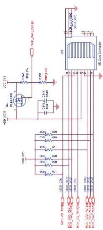
text_image
VCC 3V3 F536 1.0k 89K 1.0k 89K 1.0k 7.5k 6.5k 6.5k F544 1.0k 89K 1.0k F537 VDD MCII Q4 IPLMLC402 VCC 3V3 R343 103K T3 R357 DNP(4.7K) MCII_PWIL_PL4[IN] VCC1_C01_PE30K (MCI1_CD) MCI1_DA1 MCI1_DNE MCI1_CK MCI1_CDA MCI1_DNE MCI1_DN2 MCI1_DN2 MCI1_CDA MCI1_DNE MCI1_DN2 VDD MCII C141 IOAF C144 IOAF 224 15 15 143T 103K (MCI1_VDF) SD Card ConnectorSD/MMCPlus CARD INTERFACE - MCI1
SD/Micro SD CARD
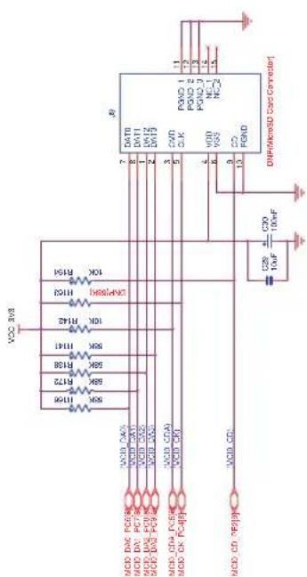
text_image
VCC 3V8 I106 R172 R138 R114 R9 R142 VCC I106 R172 R138 R114 R9 R142 VCC I106 R172 R138 R114 R9 R142 VCC I106 R172 R138 R114 R9 R142 VCC I106 R172 R138 R114 R9 R142 Vcc I106 R172 R138 R114 R9 R142 Vcc I106 R172 R138 R114 R9 R142 Vcc I106 R172 R138 R114 R9 R142 Vcc I106 R172 R138 R114 R9 R142 VCC I106 R172 R138 R114 R9 R142 Vcc I106 R172 R138 R114 R9 R142 Vcc I106 DAC PC5A I106 DAC PC7B I106 DAC PC9B I106 DAC PC9A I106 CD4 PC5B I106 CD4 PC9B I106 CD4 PC9A I106 CD I106 CD I106 CD C28 ± C30 10uF 10uF DATB DATI LVIT2 LMIT3 CVD CLK VDD VSS GND PGND 1 PGND 2 PGND 3 NC-1 NC-2 CNR(MicroSD Card Connector) INRMicro SD CARD INTERFACE - MCI0
| Atmel | ||||||
| A | B | C | D | E | F | |
| A | INT | EXT | 25 AUG 14 | XX XX | ||
| REV. | DATE | YES. | DATE## | |||
| SAM#SD#XULT | SCALE: 1/1 | FLV. | VELET | |||
| HBMCI | A | 15 | ||||
Figure 4-62. EDBG

text_image
EDBG_TWI EDBG U1 AT30JCSM455J-01LR VCC_LUGG D4 RED D5 BLUE PXD ID 06 [15] PXD ID 07 [16] PXD ID 08 [17] PXD ID 09 [20] PXD ID 10 [21] PXD ID 11 [22] PXD ID 12 [23] PXD ID 13 [24] PXD ID 14 [25] PXD ID 15 [26] PXD ID 16 [27] PXD ID 17 [28] PXD ID 18 [29] PXD ID 19 [30] PXD ID 20 [31] PXD ID 21 [32] PXD ID 22 [33] PXD ID 23 [34] PXD ID 24 [35] PXD ID 25 [36] PXD ID 26 [37] PXD ID 27 [38] PXD ID 28 [39] PXD ID 29 [40] PXD ID 30 [41] PXD ID 31 [42] PXD ID 32 [43] PXD ID 33 [44] PXD ID 34 [45] PXD ID 35 [46] PXD ID 36 [47] PXD ID 37 [48] PXD ID 38 [49] PXD ID 39 [50] PXD ID 40 [51] PXD ID 41 [52] PXD ID 42 [53] PXD ID 43 [54] PXD ID 44 [55] PXD ID 45 [56] PXD ID 46 [57] PXD ID 47 [58] PXD ID 48 [59] PXD ID 49 [60] PXD ID 50 [61] PXD ID 51 [62] PXD ID 52 [63] PXD ID 53 [64] PXD ID 54 [65] PXD ID 55 [66] PXD ID 56 [67] PXD ID 57 [68] PXD ID 58 [69] PXD ID 59 [70] PXD ID 60 [71] PXD ID 61 [72] PXD ID 62 [73] PXD ID 63 [74] PXD ID 64 [75] PXD ID 65 [76] PXD ID 66 [77] PXD ID 67 [78] PXD ID 68 [79] PXD ID 69 [80] PXD ID 70 [81] PXD ID 71 [82] PXD ID 72 [83] PXD ID 73 [84] PXD ID 74 [85] PXD ID 75 [86] PXD ID 76 [87] PXD ID 77 [88] PXD ID 78 [89] PXD ID 79 [90] PXD ID 80 [91] PXD ID 81 [92] PXD ID 82 [93] PXD ID 83 [94] PXD ID 84 [95] PXD ID 85 [96] PXD ID 86 [97] PXD ID 87 [98] PXD ID 88 [99] PXD ID 89 [100] ATmel SAMA5DH-XULT ECBG VCC_LUGG D4 RED D5 BLUE D4 RED D5 BLUE EDBG U1 AT30JCSM455J-01LR VCC_LUGG D4 RED D5 BLUE EDBG U1 AT30JCSM455J-01LR VCC_LUGG D4 RED D5 BLUE EDBG U1 AT30JCSM455J-01LR VCC_LUGG D4 RED D5 BLUE EDBG U1 AT30JCSM455J-01LR VCC_LUGGFigure 4-63. Expansion and XPRO Connectors
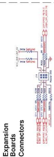
text_image
Expansion Boards Connectors EUROSP_081H E480_SP_MOS1H EPOXPRO_P020H L200_SP_SCK1H NR37_3W3 100R 1% R219 SP1_MISO_0R DINSSPR SP11_SCK_0R DINSSPR R236 R238 R229 R225 J14 Hadar 203 VCC_3W3 EXP_SN DOORP0_R24E DOORP0_R34E R352 R354 DRP0300V DRP0300V DOXPRO_P61H (T) LDOO_SP_MOS1H
text_image
XPRO Power EXP_Sy 1 2 VCC_E4 3 4 VCC_3V3 DNP Header 2X2) XPRO EXT1 EDB6 ID 02[4] 1 2 LDPXPRO_PG21[5] 3 EXPOXPRO_PG21[6] 5 PDMXPS PZ21[7] 6 PDMXPS PZ21[8] 7 PDMXPS PZ21[9] 8 PDMXPS PZ21[10] 9 PDMXPS PZ21[11] 10 PDMXPS PZ21[12] 13 PDMXPS PZ21[13] 14 PDMXPS PZ21[14] 15 PDMXPS PZ21[15] 16 PDMXPS PZ21[16] 17 PDMXPS PZ21[17] 18 PDMXPS PZ21[18] 19 PDMXPS PZ21[20] 20 PDMXPS PZ21[21] 22 PDMXPS PZ21[23] EXPOXPRO_PG26 [8] EXPOXPRO_PG26 [9] EXPOXPRO_PG26 [10] EXPOXPRO_PG26 [11] EXPOXPRO_PG26 [12] EXPOXPRO_PG26 [13] EXPOXPRO_PG26 [14] EXPOXPRO_PG26 [15] EXPOXPRO_PG26 [16] EXPOXPRO_PG26 [17] EXPOXPRO_PG26 [18] EXPOXPRO_PG26 [19] EXPOXPRO_PG26 [20] EXPOXPRO_PG26 [21] EXPOXPRO_PG26 [22] EXPOXPRO_PG26 [23] EXPOXPRO_PG26 [24] EXPOXPRO_PG26 [25] EXPOXPRO_PG26 [26] EXPOXPRO_PG26 [27] EXPOXPRO_PG26 [28] EXPOXPRO_PG26 [29] EXPOXPRO_PG26 [30] EXPOXPRO_PG26 [31] EXPOXPRO_PG26 [32] EXPOXPRO_PG26 [33] EXPOXPRO_PG26 [34] EXPOXPRO_PG26 [35] EXPOXPRO_PG26 [36] EXPOXPRO_PG26 [37] EXPOXPRO_PG26 [38] EXPOXPRO_PG26 [39] EXPOXPRO_PG26 [40] EXPOXPRO_PG26 [41] EXPOXPRO_PG26 [42] EXPOXPRO_PG26 [43] EXPOXPRO_PG26 [44] EXPOXPRO_PG26 [45] EXPOXPRO_PG26 [46] EXPOXPRO_PG26 [47] EXPOXPRO_PG26 [48] EXPOXPRO_PG26 [49] EXPOXPRO_PG26 [50] EXPOXPRO_PG26 [51] EXPOXPRO_PG26 [52] EXPOXPRO_PG26 [53] EXPOXPRO_PG26 [54] EXPOXPRO_PG26 [55] EXPOXPRO_PG26 [56] EXPOXPRO_PG26 [57] EXPOXPRO_PG26 [58] EXPOXPRO_PG26 [59] EXPOXPRO_PG26 [60] EXPOXPRO_PG26 [61] EXPOXPRO_PG26 [62] EXPOXPRO_PG26 [63] EXPOXPRO_PG26 [64] EXPOXPRO_PG26 [65] EXPOXPRO_PG26 [66] EXPOXPRO_PG26 [67] EXPOXPRO_PG26 [68] EXPOXPRO_PG26 [69] EXPOXPRO_PG26 [70] EXPOXPRO_PG26 [71] EXPOXPRO_PG26 [72] EXPOXPRO_PG26 [73] EXPOXPRO_PG26 [74] EXPOXPRO_PG26 [75] EXPOXPRO_PG26 [76] EXPOXPRO_PG26 [77] EXPOXPRO_PG26 [78] EXPOXPRO_PG26 [79] EXPOXPRO_PG26 [80] EXPOXPRO_PG26 [81] EXPOXPRO_PG26 [82] EXPOXPRO_PG26 [83] EXPOXPRO_PG26 [84] EXPOXPRO_PG26 [85] EXPOXPRO_PG26 [86] EXPOXPRO_PG26 [87] EXPOXPRO_PG26 [88] EXPOXPRO_PG26 [89] EXPOXPRO_PG26 [90] EXPOXPRO_PG26 [91] EXPOXPRO_PG26 [92] EXPOXPRO_PG26 [93] EXPOXPRO_PG26 [94] EXPOXPRO_PG26 [95] EXPOXPRO_PG26 [96] EXPOXPRO_PG26 [97] EXPOXPRO_PG26 [98] EXPOXPRO_PG26 [99] EXPOXPRO_PG26 [100] XPRO EXT2 EDB3 ID 04[4] 1 2 LDPB5 ID 05[4] 3 PDMB5 ID 07[4] 5 PDMB5 ID 08[4] 7 PDMB5 ID 09[4] 9 PDMB5 ID 10[4] 11 PDMB5 ID 11[4] 13 PDMB5 ID 12[4] 15 PDMB5 ID 13[4] 17 PDMB5 ID 14[4] 19 PDMB5 ID 15[4] 20 PDMB5 ID 16[4] 21 PDMB5 ID 17[4] 23 PDMB5 ID 18[4] 25 PDMB5 ID 19[4] 27 PDMB5 ID 20[4] 30 PDMB5 ID 21[4] 33 PDMB5 ID 23[4] 37 PDMB5 ID 30[4] 40 PDMB5 ID 31[4] 43 PDMB5 ID 33[4] 47 PDMB5 ID 35[4] 50 PDMB5 ID 37[4] 53 PDMB5 ID 39[4] 57 PDMB5 ID 40[4] 60 PDMB5 ID 41[4] 63 PDMB5 ID 43[4] 67 PDMB5 ID 45[4] 70 PDMB5 ID 47[4] 73 PDMB5 ID 49[4] 77 PDMB5 ID 50[4] 80 PDMB5 ID 51[4] 83 PDMB5 ID 53[4] 87 PDMB5 ID 55[4] 90 PDMB5 ID 57[4] 93 PDMB5 ID 59[4] 97 PDMB5 ID 60[4] 100 DXN Header 2x10) DXN Header 3x10) DXN Header 4x10) DXN Header 5x10) DXN Header 6x10) DXN Header 7x10) DXN Header 8x10) DXN Header 9x10) DXN Header 10x10) DXN Header 11x10) DXN Header 12x10) DXN Header 13x10) DXN Header 14x10) DXN Header 15x10) DXN Header 16x10) DXN Header 17x10) DXN Header 18x10) DXN Header 19x10) DXN Header 20x10) DXN Header 21x10) DXN Header 23x10) DXN Header 25x10) DXN Header 3x10) DXN Header 4x10) DXN Header 5x10) DXN Header 6x10) DXN Header 7x10) DXN Header 8x10) DXN Header 9x10) DXN Header 10x10) DXN Header 11x10) DXN Header 13x10) DXN Header 15x10) DXN Header 17x10) DXN Header 19x10) DXN Header 3x10) DXN Header 4x10) DXN Header 5x10) DXN Header 7x10) DXN Header 8x10) DXN Header 9x10) DXN Header 10x10) DXN Header 11x10) DXN Header 13x10) DXN Header 15x10) DXN Header 17x10) DXN Header 19x10) DXN Header 3x10)| A | PegA | XinCo | 11 Oct. 14 | XXX | XX XX XX |
| A | BRC EBIT | XinCo | 29 Aug. 16 | XXX | XX XX XX |
| REV | WALPF | DEC | DATE | REV. | DATE |
| SCALE: 1/1 | REV.A | SHEET15/15 | |||
text_image
J17 6009 F500 F501 F512 F513 F514 F515 F516 F517 F518 F519 F520 F521 F522 DXP[SSOR] DXP[RR] DXP[RR] DXP[RR] DXP[RR] DXP[RR] DXP[RR] DXP[RR] DXP[RR] DXP[RR] DXP[RR] DXP[RR] DXP[RR] DXP[RR] DXP[RR] DXP[RR] DXP[RR] DXP[RR] DXP[RR] DXP[RR] DXP[RR] DXP[ERR] DXP[ERR] DXP[ERR] DXP[ERR] DXP[ERR] DXP[ERR] DXP[ERR] DXP[ERR] DXP[ERR] DXP[ERR] DXP[ERR] DXP[ERR] DXP[ERR] DXP[ERR] DXP[ERR] DXP[ERR] DXP[ERR] DXP[ERR] DXP[ERR] DXP[ERR] DXP[RR] DXP[RR] DXP[RR] DXP[RR] DXP[RR] DXP[RR] DXP[RR] DXP[RR] DXP[RR] DXP[RR] DXP[RR] DXP[RR] DXP[RR] DXP[RR] DXP[RR] DXP[RR] DXP[RR] DXP[RR] DXP[RR] DXP[DR] DXP[DR] DXP[DR] DXP[DR] DXP[DR] DXP[DR] DXP[DR] DXP[DR] DXP[DR] DXP[DR] DXP[DR] DXP[DR] DXP[DR] DXP[DR] DXP[DR] DXP[DR] DXP[DR] DXP[DR] DXP[DR] DXP[DR] DXP[RR] DXP[RR] DXP[RR] DXP[RR] DXP[RR] DXP[RR] DXP[RR] DXP[RR] DXP[RR] DXP[RR] DXP[RR] DXP[RR] DXP[RR] DXP[RR] DXP[RR] DXP[RR] DXP[RR] DXP[RR] DXP[RR] DXP[QR] DXP[QR] DXP[QR] DXP[QR] DXP[QR] DXP[QR] DXP[QR] DXP[QR] DXP[QR] DXP[QR] DXP[QR] DXP[QR] DXP[QR] DXP[QR] DXP[QR] DXP[QR] DXP[QR] DXP[QR DCBSPD NCS14 DCBSPD NCS14 DCBSPD NCS14 DCBSPD NCS14 DCBSPD NCS14 DCBSPD NCS14 DCBSPD NCS14 DCBSPD NCS14 DCBSPD NCS14 DCBSPD NCS14 DCBSPD NCS14 DCBSPD NCS14
text_image
J18 1 2 3 4 5 6 7 8 9 10 11 12 13 14 15 16 17 18 19 20 21 22 23 24 25 26 27 28 29 30 31 32 33 34 35 36 37 38 39 40 41 42 43 44 45 46 47 48 49 50 51 52 53 54 55 56 57 58 59 60 61 62 63 64 65 66 67 68 69 70 71 72 73 74 75 76 77 78 79 80 81 82 83 84 85 86 87 88 89 90 91 92 93 94 95 96 97 98 99 100
flowchart
graph TD
    J16["1"] --> R00["R00"]
    J16["1"] --> R05["R05"]
    J16["1"] --> R08["R08"]
    J16["1"] --> R10["R10"]
    J16["2"] --> R00["R00"]
    J16["2"] --> R05["R05"]
    J16["2"] --> R08["R08"]
    J16["3"] --> R00["R00"]
    J16["3"] --> R05["R05"]
    J16["4"] --> R00["R00"]
    J16["4"] --> R05["R05"]
    J16["5"] --> R00["R00"]
    J16["5"] --> R05["R05"]
    J16["6"] --> R00["R00"]
    J16["6"] --> R05["R05"]
    J16["7"] --> R00["R00"]
    J16["7"] --> R05["R05"]
    J16["8"] --> R00["R00"]
    J16["8"] --> R05["R05"]
    R00["R00"] --> O3["O3"]
    R05["R05"] --> O3
    R10["R10"] --> O3
    R15["R15"] --> O3
    R20["R20"] --> O3
    R25["R25"] --> O3
    R30["R30"] --> O3
    R35["R35"] --> O3
    R40["R40"] --> O3
    R45["R45"] --> O3
    R50["R50"] --> O3
    R55["R55"] --> O3
    R60["R60"] --> O3
    R65["R65"] --> O3
    R70["R70"] --> O3
    R75["R75"] --> O3
    R80["R80"] --> O3
    R85["R85"] --> O3
    R90["R90"] --> O3
    R95["R95"] --> O3
    R105["R105"] --> O3
    R110["R110"] --> O3
    R115["R115"] --> O3
    R120["R120"] --> O3
    R125["R125"] --> O3
    R130["R130"] --> O3
    R135["R135"] --> O3
    R140["R140"] --> O3
    R145["R145"] --> O3
    R150["R150"] --> O3
    R155["R155"] --> O3
    R160["R160"] --> O3
    R165["R165"] --> O3
    R170["R170"] --> O3
    R175["R175"] --> O3
    R180["R180"] --> O3
    R185["R185"] --> O3
    R190["R190"] --> O3
    R195["R195"] --> O3
    R200["R200"] --> O3
    R205["R205"] --> O3
    R210["R210"] --> O3
    R215["R215"] --> O3
    R220["R220"] --> O3
    R225["R225"] --> O3
    R230["R230"] --> O3
    R235["R235"] --> O3
    R240["R240"] --> O3

text_image
EXP_F01A EXP_F02A EXP_F03A EXP_F04A EXP_F05A EXP_F06A EXP_F07A EXP_F08A EXP_F09A EXP_F10A EXP_F11A EXP_F12A EXP_F13A EXP_F14A EXP_F15A EXP_F16A EXP_F17A EXP_F18A EXP_F19A EXP_F20A EXP_F21A EXP_F22A EXP_F23A EXP_F24A EXP_F25A EXP_F26A EXP_F27A EXP_F28A EXP_F29A EXP_F30A EXP_F31A EXP_F32A EXP_F33A EXP_F34A EXP_F35A EXP_F36A EXP_F37A EXP_F38A EXP_F39A EXP_F40A EXP_F41A EXP_F42A EXP_F43A EXP_F44A EXP_F45A EXP_F46A EXP_F47A EXP_F48A EXP_F49A EXP_F50A EXP_F51A EXP_F52A EXP_F53A EXP_F54A EXP_F55A EXP_F56A EXP_F57A EXP_F58A EXP_F59A EXP_F60A EXP_F61A EXP_F62A EXP_F63A EXP_F64A EXP_F65A EXP_F66A EXP_F67A EXP_F68A EXP_F69A EXP_F70A EXP_F71A EXP_F72A EXP_F73A EXP_F74A EXP_F75A EXP_F76A EXP_F77A EXP_F78A EXP_F79A EXP_F80A EXP_F81A EXP_F82A EXP_F83A EXP_F84A EXP_F85A EXP_F86A EXP_F87A EXP_F88A EXP_F89A EXP_F90A EXP_F91A EXP_F92A EXP_F93A EXP_F94A EXP_F95A EXP_F96A EXP_F97A EXP_F98A EXP_F99A J10 R323 R324 1 2 3 4 5 6 7 8 9 10 11 12 13 14 15 16 17 18 19 20 21 22 23 24 25 26 27 28 29 30 31 32 33 34 35 36 37 38 39 40 41 42 43 44 45 46 47 48 49 50 51 52 53 54 55 56 57 58 59 60 61 62 63 64 65 66 67 68 69 70 71 72 73 74 75 76 77 78 79 80 81 82 83 84 85 86 87 88 89 90 91 92 93 94 95 96 97 98 99 100 XOUT XOUT XOUT XOUT XOUT XOUT XOUT XOUT XOUT XOUT XOUT XOUT XOUT XOUT XOUT XOUT XOUT XOUT XOUT XOUT XOUT XOUT XOUT XOUT XOUT XOUT XOUT XOUT XOUT XOUT XOUT XOUT XOUT XOUT XOUT XOUT XOUT XOUT XOUT XOUT XOUT XOUT XOUT XOUT XOUT XOUT XOUT XOUT XOUT XOUT X OUT XOUT XOUT XOUT XOUT XOUT XOUT XOUT XOUT XOUT XOUT XOUT XOUT XOUT XOUT XOUT XOUT XOUT XOUT XOUT XOUT XOUT XOUT XOUT XOUT XOUT XOUT XOUT XOUT XOUT XOUT XOUT XOUT XOUT XOUT XOUT XOUT XOUT X OUT X OUT X OUT X OUT X OUT X OUT X OUT X OUT X OUT X OUT X OUT X OUT X OUT X OUT X OUT X OUT X OUT X OUT X OUT X OUT X OUT X OUT X OUT X OUT X OUT X OUT X OUT X OUT X OUT X OUT X OUT X OUT X OUT X OUT X OUT X OUT X OUT X OUT X OUT X OUT X OUT X OUT X OUT X OUT X OUT X OUT X OUT X OUT X OUT X OUT X Out Y IN Y IN Y IN Y IN Y IN Y IN Y IN Y IN Y IN Y IN Y IN Y IN Y IN Y IN Y IN Y IN Y IN Y IN Y IN Y IN Y IN Y IN Y IN Y IN Y IN Y IN Y IN Y IN Y IN Y IN Y IN Y IN Y IN Y IN Y IN Y IN Y IN Y IN Y IN Y IN Y IN Y IN Y IN Y IN Y IN Y IN Y IN Y IN Y IN Y IN YIN YIN YIN YIN YIN YIN YIN YIN YIN YIN YIN YIN YIN YIN YIN YIN YIN YIN YIN YIN YIN YIN YIN YIN YIN YIN YIN YIN YIN YIN YIN YIN YIN YIN YIN YIN YIN YIN YIN YIN YIN YIN YIN YIN YIN YIN YIN YINYINYINYINYINYINYINYINYINYINYINYINYINYINYINYINYINYINYINYINYINYINYINYINYINYINYINYINYINYINYINYINYINYINYINYINYINYINYINYINYINYINYINYINYINYINYINYINYINYINYIN
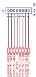
5. Revision History
In the tables that follow, the most recent version of the document appears first.
Table 5-1. SAMA5D4 Xplained Ultra User Guide Rev. 44005C Revision History
| Doc. Date Changes | |
| 11-Aug-15 | Updated Section 4.2.1 “Processor”Modified Section 4.2.2.1 “Power Lines”Modified Section 4.2.2.2 “Power-up and Power-down Considerations” (title and content) |
Table 5-2. SAMA5D4 Xplained Ultra User Guide Rev. 44005B Revision History
| Doc. Date Changes | |
| 28-Feb-15 | Minor formatting and editorial changes throughoutTable 4-3 “DDR_CALN and DDR_CALP”: added column header “Memory Type”Section 4.2.9.3 “LCD Power”: corrected “two voltage lines are available: 3.3V by default and 5 VCC” to read “two voltage lines are available: 3.3V and 5 VCC (default)”Table 4-13 “SAMA5D44 Peripheral Functions Available through the Arduino Headers”: changed column header “SAMA5D4 to Arduino” to “SAMA5D44 to Arduino”; added column header “System Function”Table 4-20 “SD/MMC Socket J24 Signal Descriptions”: defined mnemonic for pins 15 and 16 as “VSS”Table 4-21 “MicroSD Socket J9 Signal Descriptions”: for pin 9, changed mnemonic from “CARD DETECT” to “CD”; for pin 10, changed mnemonic from “PGND” to “GND” |
Table 5-3. SAMA5D4 Xplained Ultra User Guide Rev. 44005 Revision History
| Doc. Rev. Changes | |
| 44005A First issue. |
Atmel
Enabling Unlimited Possibilities®

Atmel Corporation
1600 Technology Drive, San Jose, CA 95110 USA
T: (+1)(408) 441.0311
F: (+1)(408) 436.4200
www.atmel.com
© 2015 Atmel Corporation. / Rev.: Atmel-44005C-ATARM-SAMA5D4-Xplained-Ultra-User Guide_11-Aug-15.
Atmel ^® , Atmel logo and combinations thereof, Enabling Unlimited Possibilities ^® , maXTouch ^® , QTouch ^® and others are registered trademarks or trademarks of Atmel Corporation in U.S. and other countries. ARM ^® , ARM Connected ^® logo, and others are the registered trademarks or trademarks of ARM Ltd. Other terms and product names may be trademarks of others.
DISCLAIMER: The information in this document is provided in connection with Atmel products. No license, express or implied, by estoppel or otherwise, to any intellectual property right is granted by this document or in connection with the sale of Atmel products. EXCEPT AS SET FORTH IN THE ATMEL TERMS AND CONDITIONS OF SALES LOCATED ON THE ATMEL WEBSITE, ATMEL ASSUMES NO LIABILITY WHATSOEVER AND DISCLAIMS ANY EXPRESS, IMPLIED OR STATUTORY WARRANTY RELATING TO ITS PRODUCTS INCLUDING, BUT NOT LIMITED TO, THE IMPLIED WARRANTY OF MERCHANTABILITY, FITNESS FOR A PARTICULAR PURPOSE, OR NON-INFRINGEMENT. IN NO EVENT SHALL ATMEL BE LIABLE FOR ANY DIRECT, INDIRECT, CONSEQUENTIAL, PUNITIVE, SPECIAL OR INCIDENTAL DAMAGES (INCLUDING, WITHOUT LIMITATION, DAMAGES FOR LOSS AND PROFITS, BUSINESS INTERRUPTION, OR LOSS OF INFORMATION) ARISING OUT OF THE USE OR INABILITY TO USE THIS DOCUMENT, EVEN IF ATMEL HAS BEEN ADVISED OF THE POSSIBILITY OF SUCH DAMAGES. Atmel makes no representations or warranties with respect to the accuracy or completeness of the contents of this document and reserves the right to make changes to specifications and products descriptions at any time without notice. Atmel does not make any commitment to update the information contained herein. Unless specifically provided otherwise, Atmel products are not suitable for, and shall not be used in, automotive applications. Atmel products are not intended, authorized, or warranted for use as components in applications intended to support or sustain life.
SAFETY-CRITICAL, MILITARY, AND AUTOMOTIVE APPLICATIONS DISCLAIMER: Atmel products are not designed for and will not be used in connection with any applications where the failure of such products would reasonably be expected to result in significant personal injury or death ("Safety-Critical Applications") without an Atmel officer's specific written consent. Safety-Critical Applications include, without limitation, life support devices and systems, equipment or systems for the operation of nuclear facilities and weapons systems. Atmel products are not designed nor intended for use in military or aerospace applications or environments unless specifically designated by Atmel as military-grade. Atmel products are not designed nor intended for use in automotive applications unless specifically designated by Atmel as automotive-grade.