MIC2800 - Kit d'évaluation Microchip - Free user manual and instructions
Find the device manual for free MIC2800 Microchip in PDF.

User questions about MIC2800 Microchip
0 question about this device. Answer the ones you know or ask your own.
Ask a new question about this device
Download the instructions for your Kit d'évaluation in PDF format for free! Find your manual MIC2800 - Microchip and take your electronic device back in hand. On this page are published all the documents necessary for the use of your device. MIC2800 by Microchip.
USER MANUAL MIC2800 Microchip
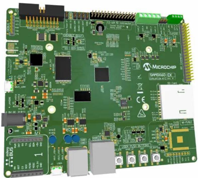
SAM9X60-EK User's Guide
Scope
This user's guide introduces the SAM9X60 Evaluation Kit (SAM9X60-EK) and describes the development and debugging capabilities running on SAM9 Arm®-based embedded MPUs.
text_image
MICROCHIP SAM9X60-EK Smart Home H15.78.1.4 SAP Capi Microchip SAP Capi Microchip SAP Capi Microchip SAP Capi Microchip SAP Capi Microchip SAP Capi Microchip SAP Capi Microchip SAP Capi Microchip SAP Capi Microchip SAP Capi Microchip SAP Capi Microchip SAP Capi Microchip SAP Capi Microchip SAPC SAPC SAPC SAPC SAPC SAPC SAPC SAPC SAPC SAPC SAPC SAPC SAPC SAPC SAPC SAPC SAPC SAPC SAPC SAPC SAPC SAPC SAPC SAPC SAPC SAPIC SAPIC SAPIC SAPIC SAPIC SAPIC SAPIC SAPIC SAPIC SAPIC SAPIC SAPIC SAPIC SAPIC SAPIC SAPIC SAPIC SAPIC SAPIC SAPIC SAPIC SAPIC SAPIC SAPIC SAPIC SAPI3 4.4 R12 4.4 R12 4.4 R12 4.4 R12 4.4 R12 4.4 R12 4.4 R12 4.4 R12 4.4 R12 4.4 R12 4.4 R12 4.4 R12 4.4 R12 4.5 R12 4.5 R12 4.5 R12 4.5 R12 4.5 R12 4.5 R12 4.5 R12 4.5 R12 4.5 R12 4.5 R12 4.5 R12 4.5 R12 4.5 R13 4.5 R13 4.5 R13 4.5 R13 4.5 R13 4.5 R13 4.5 R13 4.5 R13 4.5 R13 4.5 R13 4.5 R13 4.5 R13 4.5 R13 4.6 R13 4.6 R13 4.6 R13 4.6 R13 4.6 R13 4.6 R13 4.6 R13 4.6 R13 4.6 R13 4.6 R13 4.6 R13 4.6 R13 4.6 R14 4.6 R14 4.6 R14 4.6 R14 4.6 R14 4.6 R14 4.6 R14 4.6 R14 4.6 R14 4.6 R14 4.6 R14 4.6 R14 4.6 R15 4.6 R15 4.6 R15 4.6 R15 4.6 R15 4.6 R15 4.6 R15 4.6 R15 4.6 R15 4.6 R15 4.6Table of Contents
Scope....1
- Introduction......4
1.1. Document Layout....4
1.2. Recommended Reading....4
- Product Overview....5
2.1. SAM9X60-EK Features....5
2.2. Evaluation Kit Specifications....6
2.3. Power Sources....6
2.4. Connectors on Board....6
2.5. Default Jumper Settings....9
2.6. Kit Content....9
- Function Blocks....10
3.1. Power Supply Topology and Power Distribution....10
3.2. Processor....14
3.3. On-board Memories....29
3.4. Peripherals.... 33
3.5. User Interaction and Debugging....49
- Installation and Operation....56
4.1. System and Configuration Requirements....56
4.2. Board Setup.... 56
- Errata....57
5.1. Inoperative LED....57
5.2. Booting Issue....57
5.3. Powering-Up Issue....57
5.4. Resistor Mislabeling....58
-
Appendix. Schematics and Layouts....60
-
Revision History....67
7.1. DS50002907B - 01/2020....67
7.2. DS50002907A - 10/2019....67
The Microchip Website....68
Product Change Notification Service....68
Customer Support....68
Microchip Devices Code Protection Feature....68
Legal Notice....68
Trademarks....69
Quality Management System....69
Worldwide Sales and Service....70
1. Introduction
1.1 Document Layout
The document is organized as follows:
• Chapter 1. "Introduction"
- Chapter 2. "Product Overview" – Important information about the SAM9X60-EK board
- Chapter 3. "Function Blocks" – Specifications of the SAM9X60-EK and high-level description of the major components and interfaces
- Chapter 4. "Installation and Operation" – Instructions on how to get started with the SAM9X60-EK
- Appendix. "Schematics and Layouts" – SAM9X60-EK schematics and layout diagrams
1.2 Recommended Reading
The following Microchip document is available and recommended as a supplemental reference resource:
• SAM9X60 Datasheet. Lit. Number DS60001579
2. Product Overview
The SAM9X60-EK follows the Microchip MPU strategy for low cost evaluation kits, showcasing all the features that the SAM9X60 MPU can offer.
2.1 SAM9X60-EK Features
Table 2-1. SAM9X60-EK Features
| Characteristic Specification Featured Components | ||
| Processor 228-ball TFBGA, 11x11 mm, 0.65 mm pitch Microchip SAM9X60 | ||
| External clock | MPU: 24 MHz, 32.768 KHzMisc. osc.: 25 MHz | DSC1001CI5DSC6083CE2A |
| Memory | One 16-bit, 2-Gbit DDR2One NAND FlashOne QSPI FlashOne EEPROM | Winbond W972GG6KB-25Micron MT29F4G08ABAEAAMicrochip SST26VF064BMicrochip 24AA02E48 |
| SD/MMC One standard 4-bit SD card interface - | ||
| USB | Two stacked Type-A connectors with power switchesOne Micro-B USB Device | 2 * Microchip MIC2025 |
| CAN Two CAN interfaces Microchip MCP2542 | ||
| Ethernet One ETH port Microchip KSZ8081 | ||
| Wi-Fi/BT One optional Wi-Fi®/Bluetooth®interface Slot for Microchip ATWILC3000 | ||
| Audio One ClassD audio port - | ||
| Display | One 24-bit LCD interface | - |
| Camera | One 12-bit Image Sensor Interface | - |
| IO | One expander IO | Microchip MCP23008 |
| Debug port | One J-Link-OB + CDCOne JTAG interface | Embedded J-Link-OB through the CDC interface (ATSAM3U4C TFBGA100) |
| Board monitor | One RGB (Red, Green, Blue) LEDFour push button switches | -- |
| Expansion | One PIO connectorOne mikroBUSTMconnector | -Hundreds of possible ClickTM extensions featuring Microchip functions inside |
| Power management | Two power regulatorsTwo power consumption measurement devices | Microchip MIC2800, MCP1725Microchip PAC1934, PAC1710 |
| Board supply | From USB A or from external connector | - |
| Backup battery SuperCap - | ||
2.2 Evaluation Kit Specifications
Table 2-2. Evaluation Kit Specifications
| Characteristic Specification | |
| Board SAM9X60-EK | |
| Board supply voltage External or USB-powered | |
| Temperature | Operating: 0°C to +70°CStorage: -40°C to +85°C |
| Relative humidity 0 to 90% (non-condensing) | |
| Main board dimensions 150 × 125 × 20 mm | |
| RoHS status Compliant | |
| Board identification SAM9X60 Evaluation Kit |
2.3 Power Sources
Two options are available to power up the SAM9X60-EK board:
- Powering through an external AC to DC +5V wall adapter connector (J1)
- Powering through the USB Micro-B connector on the USBA port (J7 – default choice)
Table 2-3. Electrical Characteristics
| Electrical Parameters Value | |
| Input voltage 5VDC | |
| Maximum input voltage (limits) 6VDC | |
| Maximum 3.3VDC current 300 mA |

The SAM9X60-EK board runs at a 3.3V voltage level logic. The maximum voltage that the I/O pins can tolerate is 3.3V. Providing higher voltages (e.g., 5V) to an I/O pin could damage the board.
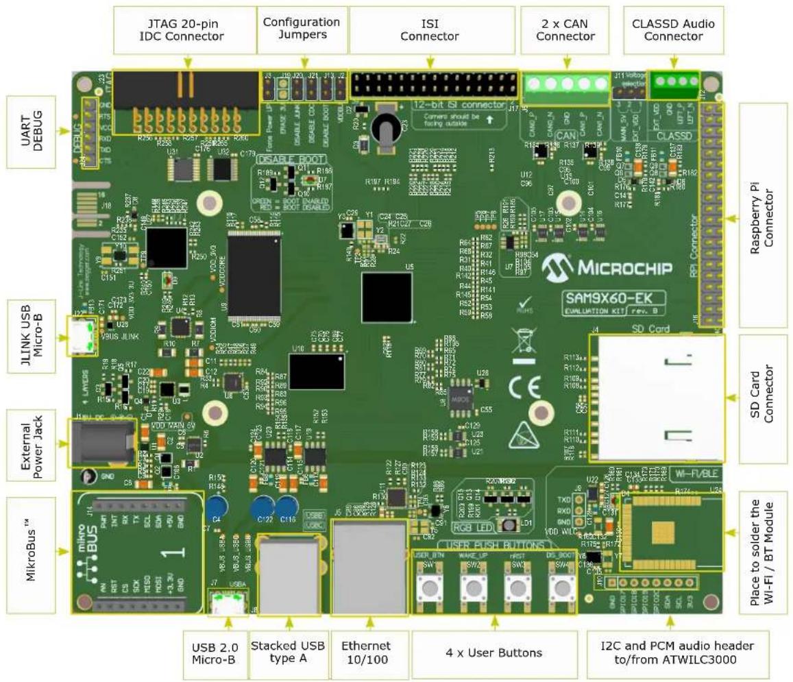
2.4 Connectors on Board
The fully-featured SAM9X60-EK board integrates multiple peripherals and interface connectors, as shown in the following figures.
Figure 2-1. SAM9X60-EK Top Connectors
text_image
JTAG 20-pin IDC Connector Configuration Jumpers ISI Connector 2 x CAN Connector CLASSD Audio Connector UART DEBUG JLINK USB Micro-B External Power Jack MikroBus™ USB 2.0 Micro-B Stacked USB type A Ethernet 10/100 4 x User Buttons I2C and PCM audio header to/from ATWILC3000 Raspberry Pi Connector MICROCHIP SAM9X60-EK EVALUATION KIT rev. B SD Card RPI Connector R325 R326 R327 R328 R329 R330 R331 R332 R333 R334 R335 R336 R337 R338 R339 R340 R341 R342 R343 R344 R345 R346 R347 R348 R349 R350 R351 R352 R353 R354 R355 R356 R357 R358 R359 R360 R361 R362 R363 R364 R365 R366 R367 R368 R369 R370 U12 C96 U12 C97 U12 C98 U12 C99 U12 C100 U12 C101 U12 C102 U12 C103 U12 C104 U12 C105 U12 C106 U12 C107 U12 C108 U12 C109 U12 C110 U12 C111 U12 C112 U12 C113 U12 C114 U12 C115 U12 C116 U12 C117 U12 C118 U12 C119 U12 C120 U12 C121 U12 C122 U12 C123 U12 C124 U12 C125 U12 C126 U12 C127 U12 C128 U12 C129 U12 C130 U12 C131 U12 C132 U12 C133 U12 C134 U12 C135 U12 C136 U12 C137 U12 C138 U12 C139 U12 C140 U12Figure 2-2. SAM9X60-EK Bottom Connectors
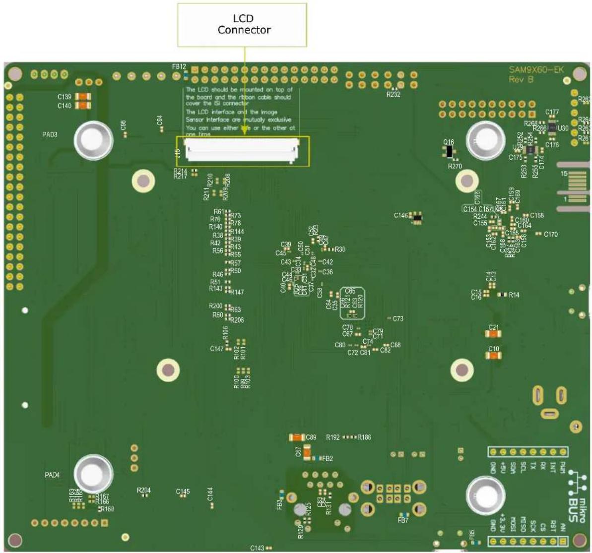
text_image
LCD Connector FB12 C139 C140 PAD9 C98 C94 R214 R217 R211 R210 R209 R206 R51 R73 R76 R78 R140 R144 R38 R39 R42 R43 R56 R55 R57 R50 R46 R51 R51 R143 R147 R200 R63 R60 R206 R106 C147 R102 R101 R000 R90 C143 PAC4 PAO4 R167 R166 R168 R204 C145 C144 C89 R192 R186 C87 FB2 FB3 FBN FBN2 FBN3 FBN4 FBN5 SAMS-60-EK Rev B C177 C176 C175 C174 C173 C172 C171 C170 C169 C168 C167 C166 C165 C164 C163 C162 C161 C160 C159 C158 C157 C156 C155 C154 C153 C152 C151 C150 C149 C148 C147 C146 C145 C144 C143 C142 C141 C140 C139 C138 C137 C136 C135 C134 C133 C132 C131 C130 C129 C128 C127 C126 C125 C124 C123 C122 C121 C120 C119 C118 C117 C116 C115 C114 C113 C112 C111 C110 C109 C108 C107 C106 C105 C104 C103 C102 C101 C99 C98 C97 C96 C95 C94 C93 C92 C91 C90 C89 R200 R209 R208 R207 R206 R205 R204 R203 R202 R201 R200 The LCD should be mounted on top of the board and the ribbon cable should cover the ISI connector. The LCD interface and the Image Sensor Interface are mutually exclusive. You can use either one or the other at one line. SAM9X60-EK Rev BTable 2-4. SAM9X60-EK Board Interface Connectors
| Connector Interfaces to | |
| J1 External power jack | |
| J4 Standard SDMMC connector | |
| J6 Dual CAN | |
| J7 USB 2.0 Micro-B (USB-A) | |
| J8A Stacked Type-A USB (USB-B) | |
| J8B Stacked Type-A USB (USB-B) | |
| J10 (not populated) ATWILC3000 GPIO | |
| J9 (not populated) ATWILC3000 UART | |
| ......continued | |
| Connector Interfaces to | |
| J5 Ethernet 10/100 RJ45 (port 1) | |
| J11 Audio external power | |
| J12 ClassD audio output | |
| J14 mikroBUS socket | |
| J15 LCD connector | |
| J16 External GPIO | |
| J17 ISI Camera Connector | |
| J18 PCB connector for factory-programming the SAM3U/J-Link-OB (not to be used by end user) | |
| J22 USB 2.0 Micro-B, J-Link-OB/J-Link-CDC | |
| J23 JTAG, 20-pin IDC | |
| J24 FTDI connector (UART debugger) |
2.5 Default Jumper Settings
Table 2-5. SAM9X60-EK Jumper Settings
| Jumper State Function | ||
| J2 Closed VDDBU current measurement | ||
| J3 | Closed Disable | the SHDN function and always keep the board powered on |
| Open (default) | Normal behavior, the PMIC can be powered down by the MPU | |
| J13 | Closed Booting | from on-board memories is permanently disabled |
| Open (default) | Booting from on-board memories is disabled only when SW4 is pressed | |
| J19(not populated) | Closed | Erase SAM3U firmware (not populated, reserved for factory configuration and should never be used by the end user) |
| Open (default) | Normal SAM3U operation (runs the J-Link interface) | |
| J20 | Closed | J-Link on-board interface is disabled. MPU debugging is done through J23, the 20-pin SAM-ICETM connector (i.e., an external JTAG interface is required) |
| Open (default) | J-Link on-board interface is enabled. MPU debugging is done through it (i.e., using the SAM3U MCU and the micro USB connector J22) | |
| J21 | Closed Disable | UART communication (CDC) between MPU and SAM3U |
| Open (default) | Enable UART communication (CDC) between MPU and SAM3U (PD20 port must be high as well) | |
2.6 Kit Content
The SAM9X60 evaluation kit includes the following:
• The SAM9X60-EK board
- USB-A to USB Micro-B cable
- 50-position FFC/FPC cable
3. Function Blocks
This section covers the specifications of the SAM9X60-EK and provides a high-level description of the board's major components and interfaces. This document is not intended to provide detailed documentation about the processor or about any other component used on the board. It is expected that the user will refer to the appropriate documents of these devices to access detailed information.
Figure 3-1. SAM9X60-EK Block Diagram
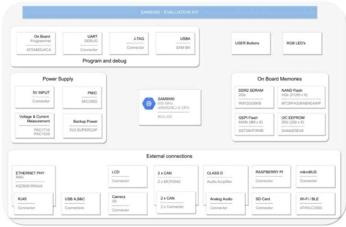
flowchart
graph TD
    A["SAM9X60 - EVALUATION KIT"] --> B["Program and debug"]
    B --> C["On Board Programmer"]
    B --> D["UART DEBUG"]
    B --> E["J-TAG"]
    B --> F["USBA"]
    B --> G["USER Buttons"]
    B --> H["RGB LED's"]

    A --> I["Power Supply"]
    I --> J["5V INPUT"]
    I --> K["PMIC"]
    I --> L["Voltage & Current Measurement"]
    I --> M["Backup Power"]
    I --> N["3V3 SUPERCAP"]

    A --> O["External connections"]
    O --> P["ETHERNET PHY RMII"]
    O --> Q["RS28061RNAIA"]
    O --> R["RJ45"]
    O --> S["USB A,B&C Connectors"]

    O --> T["LCD Connector"]
    O --> U["Camera ISI Connector"]

    O --> V["2 x CAN"]
    O --> W["2 x MCP2542"]

    O --> X["CLASS D Audio Amplifier"]
    O --> Y["Analog Audio Connector"]

    O --> Z["RASPBERRY PI Connector"]
    O --> AA["SD Card Connector"]

    O --> AB["mikroBUS Connector"]

    A --> AC["On Board Memories"]
    AC --> AD["DDR2 SDRAM 2Gb"]
    AC --> AE["W972GG6KB"]

    AC --> AF["NAND Flash 4Gb (512M x 8) MT29F4G08ABAEAWP"]

    AC --> AG["I2C EEPROM 2Kb (256 x 8) 24AA025E48"]
3.1 Power Supply Topology and Power Distribution
This section describes the implementation and the circuitry that ensures adequate voltage stability and current budget for all the devices on the board and a correct power-up sequence for the MPU. The power-up and power-down sequences indicated in the SAM9X60 datasheet must be respected for a reliable operation of the device.
3.1.1 Input Power Options
The SAM9X60-EK board can be powered through:
- an external AC to DC +5V wall adapter connected via a 2.1 mm center-positive plug into the power jack of the board (J1). The recommended output capacity of the power adapter is 2A,
- USB port A (J7).
The +5V from the wall adapter is protected through an NCP349 positive overvoltage controller switch. The controller is able to disconnect the system from its output pin when incorrect input operating conditions are detected (5.83V max).
The USB-powered operation comes from the USB device port connected to a PC or a 5VDC supply. The USB supply is enough to power the board in most applications. It is important to note that when the USB supply is used, the USB port has limited power. If USB Host port is required for the application, it is recommended that the external DC supply be used.
The switch between the two powering options is made by four transistors that ensure the separation between the two when both are plugged. The switch prioritizes powering from the wall adapter to maximize power transfer.
The following figure shows the input power supply topology.
Figure 3-2. Input Power Options

text_image
J1 2.1mm EJ508A EXT_5VDC_5V C1 10uF 25V 1206 U1 NCP349MNAETBG IN IN PAD OUT1 OUT2 EN GND FLAG 3 C2 10uF 25V 1206 C3 0.1uF 50V 0402 R2 100k 0402 5% Q1A SIA923AEDJ-T1-GE3 1 7 Q1B SIA923AEDJ-T1-GE3 8 4 VDD_MAIN_5V_ C4 100uF 16V Radial, Can QND USB_VBUS_5V FB1 180R0603 USB_5V C7 0.1uF 50V 0402 C8 10uF 25V 1206 C9 0.1uF 50V 0402 R5 100k 0402 5% Q2A SIA923AEDJ-T1-GE3 1 7 Q2B SIA923AEDJ-T1-GE3Note: USB-powered operation eliminates additional wires and batteries. It is the preferred mode of operation for any project that requires only a 5V source at up to 500 mA.
3.1.2 Power Management Integrated Circuit
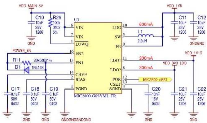
The MIC2800 is a high-performance power management IC providing three output voltages with maximum efficiency. Integrating a 2-MHz DC/DC converter with an LDO post-regulator, the MIC2800 gives two high-efficiency outputs with a second, 300 mA LDO for maximum flexibility. The DC-to-DC converter uses small values of L and C to reduce board space while still retaining efficiency over 90% at load currents up to 600 mA. For more information about the MIC2800, refer to the product web page.
Each LDO has an independent Enable (EN) pin thus allowing a proper power-up sequence for the MPU. The 20 KΩ resistor in series and the 0.1 μF capacitor in parallel with the EN1 input make a low-pass filter and introduce the necessary delay between the 3.3V and 1.15V rails needed for the proper operation of the MPU. The diode (D1 in Figure 3-3) ensures that the capacitor fast discharges during the power-down sequence.
Detailed information on the SAM9X60 MPU power supplies and power-up/down considerations are described in section "Electrical Characteristics" in the SAM9X60 device datasheet (see 1.2 Recommended Reading).
The MIC2800-G8S comes preset to supply all the voltage rails needed by the system:
- 1.8V DC/DC supplies SAM9X60 DDR2 pads (VDDIOM) and devices.
• 1.15V LDO1 supplies SAM9X60 Core (VDDCORE).
• 3.3V LDO2 supplies SAM9X60 I/O pads.
The figure below shows the power management scheme.
Figure 3-3. Power Management Integrated Circuit
text_image
VDD MAIN 5V C10 10uF 25V 1206 R29 100k 0402 5% GND POWER_EN R11 D1 20k/4021% 1N4148 C17 0.1uF 50V 0402 C18 0.1uF 50V 0402 C19 0.1uF 50V 0402 GND GND GNDGNDGND/GND U3 VIN VIN LOWQ EN2 EN1 CBYP BTAS PGND MIC2800 GSSYML TR LDO SW FB LDO1 LDO2 POR CSET SGND 600mA L1 2.2uH 11 300mA 300mA VDD 1V15 VDD 3V3 LDO MIC2800 nRST C20 10nF 16V 0402 GND GND GNDGND C11 10uF 25V 1206 C12 10uF 25V 12063.1.3 Shutdown Circuitry
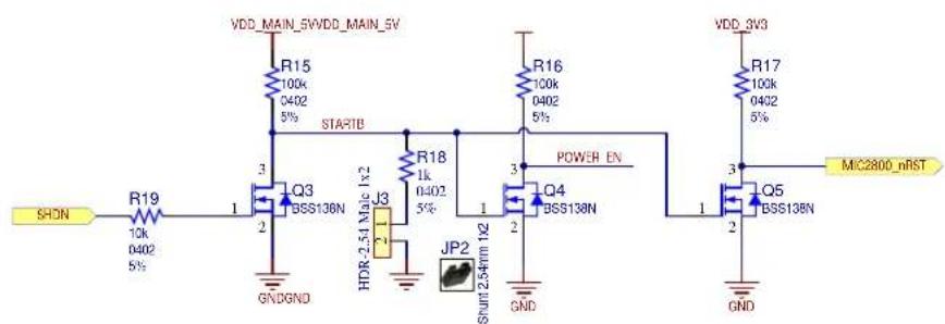
The processor can assert the SHDN signal to shut down the PMIC and enter Power-down mode. This is done by pulling both enable pins of the PMIC to GND through a Field Effect Transistor (FET) scheme.
Jumper J3 must not be set to enable this functionality. By setting jumper JP2/J3, the user can shut down the MPU without powering down its power rails.
Figure 3-4. Shutdown Circuitry
text_image
VDD_MAIN_5WVDD_MAIN_5V R15 100k 0402 5% STARTB R16 100k 0402 5% POWER EN R17 100k 0402 5% MIC2800_nRST SHDN R19 10k 0402 5% Q3 BSS138N J3 HDR-2.54 Male 1x2 JP2 Shunt 2.54mm 1x2 GNDGND Q4 BSS138N VDD_SV3 R17 100k 0402 5% GND Q5 BSS138N3.1.4 Battery Unit
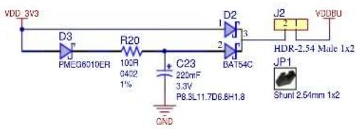
A 3.3V battery (supercapacitor) is implemented to permanently maintain the VDDBU voltage.
This function allows the user to shut down the MPU and the system, thus entering a low power mode, and still keep the custom configuration that was previously set in the MPU backup area. While in Shut-down mode, the board can be woken up by action on the SW2 button (WAKE UP), which signals the MPU to resume operations.
Jumper JP1/J2 must be in place for proper operation of the MPU, and can be removed if the user wants to bring the MPU back to the initial configuration, by resetting the General Purpose Backup Registers (GPBR).

Make sure the board is powered off before removing the JP1/J2 jumper.
Figure 3-5. Battery Unit
text_image
VDD 3V3 D3 PMEG6010ER R20 100R 0402 1% C23 220mF 3.3V P8.3L11.7D6.8H1.8 BAT54C D2 J2 1 VQDBU HDR-2.54 Male 1x2 JP1 Shunt 2.54mm 1x23.1.5 Current Measurement
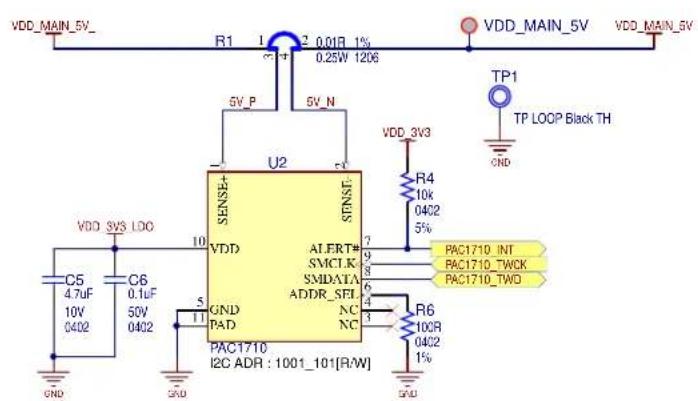
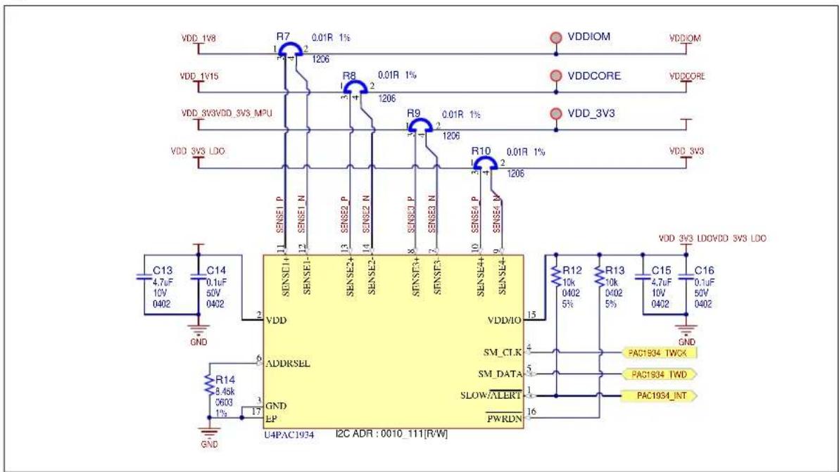
Two Microchip DC power/energy monitors are embedded on the SAM9X60-EK board:
• one single high-side current sense monitor PAC1710
• one four-channel current sense monitor PAC1934
Both chips communicate with the MPU via a Two-wire Interface (TWI) and both output their ALERT# signal to a port expander.
The PAC1710 is a single high-side bidirectional current sensing monitor with precision voltage measurement capabilities. The power monitor measures the voltage developed across an external sense resistor to represent the high-side current of a battery or voltage regulator. The PAC1710 also measures the SENSE+ pin voltage and calculates average power over the integration period. The PAC1710 can be programmed to assert the ALERT# pin when high and low limits are exceeded for current sense and bus voltage. For more information about the PAC1710, refer to the product web page.
One current sense resistor is populated on board for measuring voltage and current on the main 5V power rail.
Figure 3-6. PAC1710 Current Measurement
text_image
VDD_MAIN_5V_ R1 1 2 0.01R 1% 0.25W 1206 VDD_MAIN_5V VDD_MAIN_5V 5V_P 5V_N U2 SENSE+ STNST- VDD_3V3 R4 10k 04C2 5% TP1 TP LOOP Black TH VDD_3V3 C5 4.7uF C6 0.1uF 10V 50V 0402 GND GND PAD PAC1710 I2C ADR : 1001_101[R/W] ALERT# SMCI.K SMDATA ADDR_SEL NC NC 7 9 8 5 4 3 R6 10CR 04C2 1% PAC1710_INT PAC1710_TWCK PAC1710_TWOTable 3-1. PAC1710 Signal Descriptions
| PIO Signal Name Shared PIO Signal Description | |||
| PA31 PAC1710_TWCK Power TWI TWI clock | |||
| PA30 PAC1710_TWD | Power TWI TWI data | ||
| - | PAC1710_INT | - | Interrupt – to port expander U6 |
The PAC1934 is a four-channel power/energy monitor with current sensor amplifier and bus voltage monitors that feed high resolution ADCs. Digital circuitry performs power calculations and energy accumulation. The PAC1934 enables energy monitoring with integration periods from 1 ms to up to 36 hours. Bus voltage, sense resistor voltage, and accumulated proportional power are stored in registers for retrieval by the system master or embedded controller. For more information about the PAC1934, refer to the product web page.
Four current sense resistors are populated on board for measuring voltage and current consumption on the power rails:
• 3.3V VDD_3V3_MPU - MPU on the 3.3V rail
- 3.3V VDD_3V3_SYS - rest of the system on the 3.3V rail
• 1.8V VDDIOM - MPU and DDR2 memory
• 1.15V VDDCORE – MPU core
Figure 3-7. PAC1934 Current Measurement
text_image
VDD_1V8 R7 0.01R 1% 1206 VDD_1V15 R8 0.01R 1% 1206 VDD_3V3VDD_3V3 MPU R9 0.01R 1% 1206 VDD_3V3 LDO R10 0.01R 1% 1206 VDD_3V3 C13 4.7uF 10V 0402 C14 0.1uF 50V 0402 GND SENSE1 P SENSE1- SENSE2 P SENSE2- SENSE3 P SENSE3- SENSE4 P SENSE4 N SENSE4 N SENSE4- VDD ADDRSEL GND EP U4PAC1934 I2C ADR : 0010_111[R/W] VDD/IO SM_CTK SM_DATA SLOW/ALERT PWRDN R12 10k 0402 5% R13 10k 0402 5% C15 4.7uF 10V 0402 C16 0.1uF 50V 0402 GND PAC1934 TWCK PAC1934 TWD PAC1934_INTTable 3-2. PAC1934 Signal Descriptions
| PIO Signal Name Shared PIO Signal Description | ||
| PA31 PAC1934_TWCK Power TWI TWI clock | ||
| PA30 PAC1934_TWD Power TWI TWI data | ||
| - PAC1934_INT - Interrupt - to port expander U6 |
3.2 Processor
The SAM9X60 is a high-performance, ultra-low power ARM926EJ-S CPU-based embedded microprocessor (MPU) running up to 600 MHz, with support for multiple memories such as SDRAM, LPSDRAM, LPDDR, DDR2, QSPI and e.MMC Flash. The device integrates powerful peripherals for connectivity and user interface applications, and offers security functions (tamper detection, etc.), TRNG, as well as high-performance crypto accelerators for AES and SHA.
Refer to the SAM9X60 datasheet for more information (see 1.2 Recommended Reading).
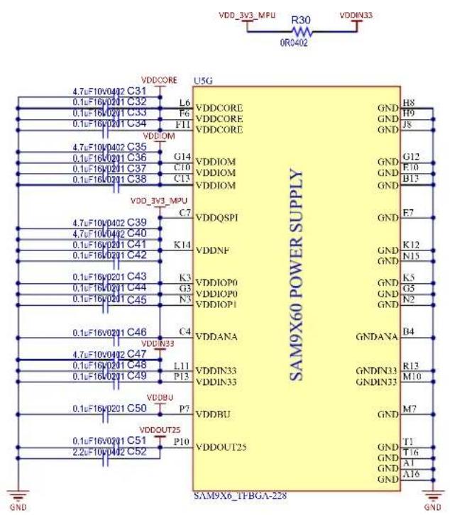
3.2.1 Power Supply
The PMIC (main regulator) provides all power supplies required by the SAM9X60 device:
• 1.15V for VDDCORE
- 1.8V for VDDIOM
• 3.3V for VDDIOP0, VDDIOP1, VDDANA, VDDNF, VDDQSPI, VDDIN33 and VDDBU
Decoupling capacitors are placed close to the MPU power pins to stabilize the voltage rails.
Figure 3-8. Processor Power Supplies
text_image
VDD_3V3_MPU R30 VDDIN33 0RC402 VDD3V3_MPU U5G 4.7uF10v0402 C31 0.1uF16v0201 C32 0.1uF16v0201 C33 0.1uF16v0201 C34 VDDIOM 4.7uF10v0402 C35 0.1uF16v0201 C36 0.1uF16v0201 C37 0.1uF16v0201 C38 G14 C10 C13 VDD_3V3_MPU 4.7uF10v0402 C39 4.7uF10v0402 C40 0.1uF16v0201 C41 0.1uF16v0201 C42 K14 K3 G3 GNDQSPI VDDNF VDDIOP0 VDDIOP0 VDDIOP1 VDDANA VDDIN33 L11 P13 VDDBU P7 VDDOUT25 2.2uF16v0201 C50 VDDOUT25 P10 VDDOUT25 VDDIN33 GNDANA GNDIN33 GNDIN33 GND GNDOUT25 VDDOUT25 SAM9X60 POWER SUPPLY GND GNDIN33 GNDIN33 GNDIN33 GNDIN33 GNDIN33 GNDIN33 GNDIN33 GNDIN33 GNDIN33 GNDIN33 GNDIN33 GNDIN33 GNDIN33 GNDIN33 GNDIN33 GNDIN33 GNDIN33 GNDN GNDOUT25 VDDOUT25 SAM9X6_TFBGA-2283.2.2 Main Configuration and Control
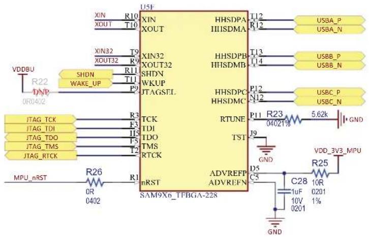
This block depicts the main block for processor configuration and control:
- XIN and XOUT are the Main Clock Oscillator input/output.
- XIN32 and XOUT32 are the Slow Clock Oscillator input/output.
- SHDN is an output signal used to enable and disable an external power supply circuit.
- WKUP is an event detection input pin used to wake up the processor from Shutdown state.
- JTAGSEL is an input that when pulled high enables the JTAG boundary scan.
• TCK, TDI, TDO, TMS and RTCK are used for JTAG communication. - nRST is the processor main reset input.
- HHSD_A/B/C are the three USB ports embedded inside the MPU.
- RTUNE is used for USB external tuning.
- TST input is reserved for processor manufacturing tests.
- ADVREFP and ADVREFN are the positive and negative reference points for the embedded analog comparator. A small low-pass filter is placed to reduce the input noise and improve accuracy.
Figure 3-9. Processor Main Configuration and Control
text_image
U5F XIN R10 XOUT T10 XIN32 T9 XOUT32 R9 SHDN R11 WAKE_UP T11 P9 JTAGSTL TCK TDI TDO TMS RTCK R26 OR 0402 nRST SAM9x0_TFBGA-228 HHSDPA T12 HHSDMA R12 HHSDPB T13 HHSDMB U14 HHSDPC P12 HHSDMC N12 RTUNE P11 R23 5.62k 04021% J9 GND D5 C5 ADVREFP ADVREFN VDD_3V3_MPU R25 C28 10R 1uF 0201 1% 10V 0201 GND3.2.3 Clock Circuitry
The embedded MPU generates its necessary clocks based on two oscillators: one slow clock (SLCK) oscillator running at 32.768 kHz and one main clock oscillator running at 24 MHz.
The main clock oscillator is implemented with a MEMS (Micro Electro-Mechanical System) device DSC1001.
For evaluation purposes, we leave users the freedom to mount a crystal instead, using the PCB footprint reservation (Y1). In that case, resistors R149 and R28 should be removed, resistors R27 and R91 should be populated and capacitors C24 and C25 should be populated with the appropriate load capacitance for the selected crystal.
Figure 3-10. Processor Clock Circuitry

text_image
C26 0402 GND C27 20pF Y2 32.768KHz ABS06-32.768KHZ-T 20pF0402 XIN32 DNP 524 1M 042 6% XOUT32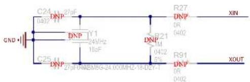
text_image
C24 DNP 0402 11 GND C25 DNP 27p-0482M5G-24.00MHz-18-D2Y-T DNP IY1 24VHz 18pF R21 TM 0402 5% R27 DNP 0R 0402 R91 DNP 0R 0402 XIN XOUT
text_image
VDD_3V3 C29 0.1uF 50V 0402 GND GND Y3 VDD OUT GND STR 24MHz DSC1001C15-024.0000 R149 51R 0402 TP2 XIN R28 0R 0402 XOUT3.2.4 Reset Circuitry
Three reset sources for the SAM9X60 MPU are placed on the board:
• Power-on Reset from the power management unit MIC2800
- User push button reset SW3
- External JTAG or J-Link-OB reset from an in-circuit emulator
Figure 3-11. Processor Reset Circuitry
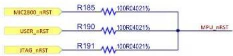
text_image
MIC2800_nRST R185 100R34021% USER_nRST R190 100R34021% JTAG_nRST R191 100R34021% MPU_nRST3.2.5 DDR Controller (MPDDRC)
The SAM9X60 embeds a Multi-Port DDR-SDRAM Controller (MPDDRC) to drive DDR2 and LPDDR1 memories.
Note the following regarding the command and control signal connections between the DDR Controller and the DDR Memory:
- Addresses A0, A1 and A12 are not used on the controller side.
- Addresses A2 to A11 are connected to A0 to A9 on the memory side.
• Signal SDA10 must be connected to A10. - Addresses A13 to A15 are connected to the last three addresses on the memory side.
• A16 to A18 are connected to BA0 to BA2.
It is recommended to double-check the design schematic against the information provided in the datasheet.
Figure 3-12. Processor DDR Controller
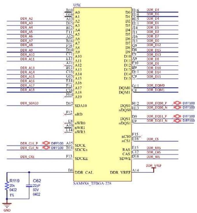
The MPDDRC I/Os embed an automatic impedance matching control to avoid overshoots and to reach the best performance levels depending on the bus load and external memories. A serial termination connection scheme, where the driver has an output impedance matched to the characteristic impedance of the line, is used to improve signal quality and reduce EMI. This is done using the ZQ calibration procedure to calibrate the SAM9X60 DDR I/O drive strength. The pin name where the ZQ resistor must be connected is DDR_CAL and, as indicated in the SAM9X60 datasheet for DDR2 case, the resistor value is 20 KOhms.
The DDR_VREF pin serves as a voltage reference input for the DDR I/Os when DDR2 or LPDDR external SDRAM memories are used.
Figure 3-13. DDR Reference Voltage

text_image
VDD/OM C65 4.7uF 10V 0402 GND C63 0.1uF 16V 0201 R120 4.7k 0201 1% C66 0.1uF 16V 0201 R121 4.7k 0201 1% DOR_VREF3.2.6 PIOs
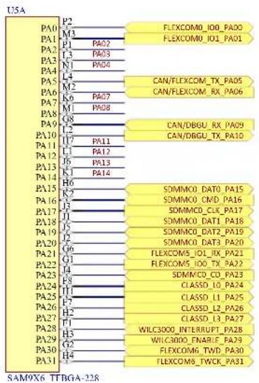
The following sections depict all the signals connected to the SAM9X60 MPU ports.
See Table 3-3 for details about each port's functions.
Figure 3-14. Processor PIOs PA and PC
text_image
I15A PA0 P2 FLEXCOM0_IO0_PA00 M3 FLEXCOM0_IO1_PA01 PA1 P1 PA02 L3 L4 CAN/FLEXCOM_TX_PA05 P2 P3 CAN/FLEXCOM_RX_PA06 PA2 P4 P4 L5 P5 CAN/DBGU_RX_PA09 M6 P6 CAN/DBGU_TX_PA10 PA3 P7 P7 L8 P8 L9 P9 PA10 P10 L10 P11 L11 P12 PA11 P13 L12 P14 PA12 P15 L13 P16 PA13 P17 PA14 P18 PA15 P19 PA16 P20 PA17 P21 PA18 P22 PA19 P23 PA20 P24 PA21 P25 PA22 P26 PA23 P27 PA24 P28 PA25 P29 PA26 P30 PA27 P31 PA28 P32 PA29 P33 PA30 P34 PA31 P35 P4 FLEXCOM6_TWD_PA30 F4 FLEXCOM6_TWCK_PA31 SDMMC0_DAT0_PA15 SDMMC0_CMD_PA16 SDMMC0_CLK_PA17 SDMMC0_DAT1_PA18 SDMMC0_DAT2_PA19 SDMMC0_DAT3_PA20 FLEXCOM5_IO1_RX_PA21 FLEXCOM5_IO0_TX_PA22 SDMMC0_CO_PA23 CLASSD_10_PA24 CLASSD_L1_PA25 CLASSD_L2_PA26 CLASSD_L3_PA27 WILC3000_INTERRUPT_PA28 WILC3000_ENABLE_PA29 FLEXCOM6_TWCK_PA31
text_image
USC M4 PC0 P4 PC1 N5 PC2 P5 PC3 L5 PC4 R4 PC5 M6 PC6 L3 PC7 N8 PC8 L4 PC9 P6 PC10 N6 PC11 R5 PC12 L7 PC13 T5 PC14 J7 PC15 R6 PC16 K8 PC17 T0 PC18 L8 PC19 P8 PC20 M8 PC21 R7 PC22 K9 PC23 R8 PC24 T9 PC25 L10 PC26 M9 PC27 N9 PC28 L10 PC29 T7 PC30 M13 PC31 LCD_D0_ISI_D0_PC00 LCD_D1_ISI_D1_PC01 LCD_D2_ISI_D2_PC02 LCD_D3_ISI_D3_PC03 LCD_D4_ISI_D4_PC04 LCD_D5_ISI_D5_PC05 LCD_D6_ISI_D6_PC06 LCD_D7_ISI_D7_PC07 LCD_D8_ISI_D8_PC08 LCD_D9_ISI_D9_PC09 LCD_D10_ISI_D10_PC10 LCD_D11_ISI_D11_PC11 LCD_D12_ISI_PCK_PC12 LCD_D13_ISI_VSYNC_PC13 LCD_D14_ISI_HSYNC_PC14 LCD_D15_ISI_MCK_PC15 LCD_D16_ISI_nRST_PC16 LCD_D17_PC17 LCD_D18_PC18 LCD_D19_PC19 LCD_D20_PC20 LCD_D21_PC21 LCD_D22_PC22 LCD_D23_PC23 LCD_ISI_ENABLE_PC24 LCD_IRQ1_PC25 LCD_PWM_PC26 LCD_VSYNC/CS_PC27 LCD_HSYNC/WL_PC28 LCD_DATA_ENABLE_PC29 LCD_PCLK_PC30Figure 3-15. Processor PIOs PB and PD
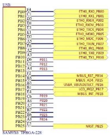
text_image
USB PB01 F4 C1 D3 D2 D1 F3 E1 D2 A5 F6 A2 A3 P811 P812 P813 P12 B5 B3 B1 F4 C6 PB19 A6 PB20 A7 PB21 B7 PB22 B6 PB23 A8 PB24 F2 ETHO_RXO_PR00 ETHO_RX1_PB01 ETHO_RXER_PB02 ETHO_RXDV_PB03 ETHO_TXCK_PB04 ETHO_MDDI_PR05 ETHO_MDC_P306 ETHO_TXEN_PB07 ETHO_IRQ_PB08 ETHO_TXO_PB09 ETHO_TX1_PB10 MBUS_RST_PB14 MBUS_A0M_PB15 USBA_VBUSDETECT_PB16 LCD_IRQ2_PB17 MBUS_INT_PB18 NRST_PB25 SAM9X6 TFBGA-228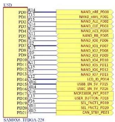
text_image
LSD PD0 R14 NAND_rRF_PD00 PD1 T15 NAND_rWE_PD01 PD2 P15 NAND_ALE_PD02 PD3 N14 NAND_CIF_PD03 PD4 R16 NAND_IC5_PD04 PD5 N11 NAND_RC_PD05 PD6 K16 NAND_IOI_PD06 PD7 J12 NAND_IO1_PD07 PD8 K15 NAND_IO2_PD08 PD9 L16 NAND_IO3_PD09 PD10 K11 NAND_IO4_PD10 PD11 L15 NAND_IO5_PD11 PD12 J15 NAND_IO6_PD12 PD13 L12 NAND_IO7_PD13 PD14 LCD_ID_PD14 PD15 M16 USBB EN_5V_PD15 PD16 M14 USBC EN_5V_PD16 PD17 N16 MCP23008_INT_PD17 PD18 L13 USER_BUTTON_PD18 PD19 P16 SEL_FNCT1_PD19 PD20 M11 SEL_FNCT2_PD20 PD21 M15 CAN_STBY_PD21 SAM9X6_IFBGA-228Some of the ports were multiplexed to accommodate more devices on the evaluation kit and to showcase all the functions the SAM9X60 MPU can address off a single PIO wire.
Most of the ports that share multiple functions are split through passive resistors placed on the board as close to the MPU as possible, therefore no other hardware change must be made. In most cases, the user can use only one of their functions at a time, or can develop a composite driver enabling the use of multiple functions at the same time.
Figure 3-16. Processor PIO Muxing

bar
| Module | Power (%) | |---|---| | PA02 | R31 22R04021% SDMMC1_WILC3000_DAT1_PA02 EXT40_GPIO_PA02 | | PA03 | R38 22R04021% SDMMC1_WILC3000_DAT2_PA03 EXT40_GPIO_PA03 | | PA04 | R40 22R04021% SDMMC1_WILC3000_DAT3_PA04 EXT40_GPIO_PA04 | | PA07 | R42 22R04021% FLEXCOM5_IO4_BT_RTS_PA07 EXT40_NPCS1_PA07 | | PA08 | R44 22R04021% FLEXCOM5_IO3_BT_CTS_PA08 EXT40_NPCS2_PA08 | | PA11 | R46 22R04021% SDMMC1_WILC3000_DAT0_PA11 MBUS_MISO_PA11 EXT40_SPI_MISO_PA11 | | PA12 | R52 22R04021% SDMMC1_WILC3000_CMD_PA12 MBUS_MOSI_PA12 EXT40_SPI_MOSI_PA12 | | PA13 | R55 22R04021% SDMMC1_WILC3000_CX_PA13 MBUS_SPCK_PA13 EXT40_SPI_SCLK_PA13 | | PA14 | R58 22R04021% MBUS_NPCS0_PA14 EXT40_GPIO_PA14 |
text_image
PB11 R60 0R0402 PB12 R63 0R0402 PB13 R65 0R0402 PB19 R69 22R04021% PB20 R71 22R04021% PB21 R74 22R04021% PB22 R77 22R04021% PB23 R80 22R04021% PB24 R82 22R04021% PC31 R86 22R04021% EXT40_PWM0_PB11 LED_RED_PB11 EXT40_PWM2_PB12 LED_GREEN_PB12 MBUS_PWM_PB13 EXT40_CLKP_PB13 LED_BLUE_PB13 EXT40_12SCK_PB19 QSPI_SCK_PB19 EXT40_12SWS_PB20 QSPI_CS_PB20 EXT40_12SDIN_PB21 QSPI_IOI_PB21 EXT40_12SDOUT_PB22 QSPI_IOI_PB22 EXT40_12SMCK_PB23 QSPI_IO2_PB23 EXT40_GPIO_PB24 QSPI_IO3_PB24 EXT40_CUK1_PC31 ETHO_PCK1_PC31Table 3-3. Processor PIOs Pin Assignment and Signal Description
| Pad Power Rail Function I/O Type | ||
| PA0 VDDIOP0 (3.3V) FLEXCOM0_IO0 | TWI Data (TWD) bidirectional line shared between the LCD, EEPROMs and external 40-pin header | |
| PA1 VDDIOP0 (3.3V) FLEXCOM0_IO1 | TWI Clock (TWCK) output line shared between the LCD, EEPROMs and external 40-pin header | |
| Pad Power Rail Function I/O Type | |||
| PA2 VDDIOP0 (3.3V) | SDMMC1_DAT1 | SDIO Data 1 (I/O1) bidirectional line for the ATWILC3000 Wi-Fi/BT module | |
| GPIO GPIO going to the external 40-pin header | |||
| PA3 VDDIOP0 (3.3V) | FLEXCOM0_IO3 | SDIO Data 2 (I/O2) bidirectional line for the ATWILC3000 Wi-Fi/BT module | |
| GPIO GPIO going to the external 40-pin header | |||
| PA4 VDDIOP0 (3.3V) | FLEXCOM0_IO2 | SDIO Data 3 (I/O3) bidirectional line for the ATWILC3000 Wi-Fi/BT module | |
| GPIO GPIO going to the external 40-pin header | |||
| PA5^1 | VDDIOP0 (3.3V) | FLEXCOM1_IO0 UART Transmit (TX) output line going to the external 40-pin header | |
| CANTX1 | CAN Transmit (CANTX) output line going to the second CAN transceiver MCP2542 | ||
| PA6^1 | VDDIOP0 (3.3V) | FLEXCOM1_IO1 UART Receive (RX) input line going to the external 40-pin header | |
| CANRX1 | CAN Receive (CANRX) input line going to the second CAN transceiver MCP2542 | ||
| PA7 VDDIOP0 (3.3V) | FLEXCOM4_IO4 First SPI Chip Select (nCS) output line for the external 40-pin header | ||
| FLEXCOM5_IO4 SPI Request to Send (RTS) output line for the BT module | |||
| PA8 VDDIOP0 (3.3V) | FLEXCOM4_IO5 | Second SPI Chip Select (nCS) output line for the external 40-pin header | |
| FLEXCOM5_IO3 SPI Clear to Send (CTS) input line for the BT module | |||
| PA9^2 | VDDIOP0 (3.3V) | DRXD DEBUG UART Receive (DRX) input line | |
| CANRX0 | CAN Receive (CANRX) input line going to the first CAN transceiver MCP2542 | ||
| PA10^2 | VDDIOP0 (3.3V) | DTXD DEBUG UART Transmit (DTX) input line | |
| CANTX0 | CAN Transmit (CANTX) output line going to the first CAN transceiver MCP2542 | ||
| PA11 VDDIOP0 (3.3V) | FLEXCOM4_IO1 | SPI Master Input Slave Output (MISO) input line shared between the mikroBUS and external 40-pin connectors | |
| SDMMC1_DAT0 | SDIO Data 0 (I/O0) bidirectional line going to the ATWILC3000 Wi-Fi/BT module | ||
| PA12 VDDIOP0 (3.3V) | FLEXCOM4_IO0 | SPI Master Output Slave Input (MOSI) output line shared between the mikroBUS and external 40-pin connectors | |
| SDMMC1_CMD | SDIO Command (CMD) bidirectional line going to the ATWILC3000 Wi-Fi/BT module | ||
| PA13 VDDIOP0 (3.3V) | FLEXCOM4_IO2 | SPI Source Clock (SCLK) output line shared between the mikroBUS and external 40-pin connectors | |
| SDMMC1_CK | SDIO Data 0 (I/O0) bidirectional line going to the ATWILC3000 Wi-Fi/BT module | ||
| PA14 VDDIOP0 (3.3V) | FLEXCOM4_IO3 SPI Chip Select (nCS) output line for the mikroBUS connector | ||
| GPIO GPIO going to the external 40-pin header | |||
| Pad Power Rail Function I/O Type | |||
| PA15 | VDDIOP0 (3.3V) | SDMMC0_DAT0 SDIO | Data 0 (I/O0) bidirectional line going to the SD card connector |
| PA16 | VDDIOP0 (3.3V) | SDMMC0_CMD | SDIO Command (CMD) bidirectional line going to the SD card connector |
| PA17 | VDDIOP0 (3.3V) | SDMMC0_CK SDIO | Clock (CLK) output line going to the SD card connector |
| PA18 | VDDIOP0 (3.3V) | SDMMC0_DAT1 SDIO | Data 1 (I/O1) bidirectional line going to the SD card connector |
| PA19 | VDDIOP0 (3.3V) | SDMMC0_DAT2 SDIO | Data 2 (I/O2) bidirectional line going to the SD card connector |
| PA20 | VDDIOP0 (3.3V) | SDMMC0_DAT3 SDIO | Data 3 (I/O3) bidirectional line going to the SD card connector |
| PA21 | VDDIOP0 (3.3V) | FLEXCOM5_IO1 | UART Receive (RX) input line shared between the mikroBUS connector and the BT transceiver on the ATWILC3000 module |
| PA22 | VDDIOP0 (3.3V) | FLEXCOM5_IO0 | UART Transmit (TX) output line shared between the mikroBUS connector and the BT transceiver on the ATWILC3000 module |
| PA23 | VDDIOP0 (3.3V) | GPIO | GPIO used as input to detect when an SD card has been inserted in the SD connector |
| PA24 | VDDIOP0 (3.3V) | CLASSD_L0 CLASSD | Left Output L0 |
| PA25 | VDDIOP0 (3.3V) | CLASSD_L1 CLASSD | Left Output L1 |
| PA26 | VDDIOP0 (3.3V) | CLASSD_L2 CLASSD | Left Output L2 |
| PA27 | VDDIOP0 (3.3V) | CLASSD_L3 CLASSD | Left Output L3 |
| PA28 | VDDIOP0 (3.3V) | GPIO / WKUP4 | GPIO Input used to signal any interrupt coming from the WILC300 Wi-Fi/BT module |
| PA29 | VDDIOP0 (3.3V) | GPIO | GPIO Output used to enable the WILC300 Wi-Fi/BT module by enabling its power supply |
| PA30 | VDDIOP0 (3.3V) | FLEXCOM6_IO0 | TWI Data (TWD) bidirectional signal shared between PAC1934, PAC1710, MPC23008 and the mikroBUS connector |
| PA31 | VDDIOP0 (3.3V) | FLEXCOM6_IO1 | TWI Clock (TWCK) Bidirectional signal shared between PAC1934, PAC1710, MPC23008 and the mikroBUS connector |
| PB0 | VDDANA (3.3V) | E0_RX0 RMII Ethernet | Receive Data 0 signal going to KSZ8081 |
| PB1 | VDDANA (3.3V) | E0_RX1 RMII Ethernet | Receive Data 1 signal going to KSZ8081 |
| PB2 | VDDANA (3.3V) | E0_RXER RMII Ethernet | Receive Error signal going to KSZ8081 |
| PB3 | VDDANA (3.3V) | E0_RXDV RMII Ethernet | Receive Data Valid signal going to KSZ8081 |
| PB4 | VDDANA (3.3V) | E0_TXCK RMII Ethernet | Transmit Clock signal going to KSZ8081 |
| PB5 | VDDANA (3.3V) | E0_MDIO RMII Ethernet | Management Data I/O signal going to KSZ8081 |
| PB6 | VDDANA (3.3V) | E0_MDC RMII Ethernet | Management Data Clock signal going to KSZ8081 |
| PB7 | VDDANA (3.3V) | E0_TXEN RMII Ethernet | Receive Data Valid signal going to KSZ8081 |
| PB8 | VDDANA (3.3V) | E0_TXER RMII Ethernet | Transmit Coding Error signal going to KSZ8081 |
| PB9 | VDDANA (3.3V) | E0_TX0 RMII | Ethernet Transmit Data 0 signal going to KSZ8081 |
| PB10 | VDDANA (3.3V) | E0_TX1 | RMII Ethernet Transmit Data 1 signal going to KSZ8081 |
| PB11 | VDDANA (3.3V) | PWM0 | PWM signal shared between the LD1 red LED and the 40-pin connector |
| PB12 VDDANA (3.3V) PWM1 | PWM signal shared between the LD1 green LED and the 40-pin connector | ||
| PB13 VDDANA (3.3V) PWM2 | PWM signal shared between the LD1 blue LED, the mikroBUS and the 40-pin connectors | ||
| PB14 VDDANA (3.3V) GPIO GPIO output used as the reset signal for the mikroBUS connector | |||
| PB15 VDDANA (3.3V) AD4 Analog input for the mikroBUS connector | |||
| PB16 VDDANA (3.3V) GPIO | GPIO input used to detect if the board has been connected to a host on the USBA port | ||
| PB17 VDDANA (3.3V) GPIO GPIO input used to signal any interrupt request from the LCD | |||
| PB18 VDDANA (3.3V) GPIO | GPIO input used to signal any interrupt request from the mikroBUS connector | ||
| PB19 VDDQSPI (3.3V) | QSCK QSPI Serial Clock (SCK) signal going to SST26VF064B | ||
| I2SMCC_CK I2S Bit Clock (CK) signal going to the 40-pin connector | |||
| PB20 VDDQSPI (3.3V) | QCS QSPI Chip Select (CS) signal going to SST26VF064B | ||
| I2SMCC_WS I2S Word Select (WS) signal going to the 40-pin connector | |||
| PB21 VDDQSPI (3.3V) | QIO0 QSPI Data I/O 0 (IO0) signal going to SST26VF064B | ||
| I2SMCC_DINO I2S Data IN 0 (DINO) signal going to the 40-pin connector | |||
| PB22 VDDQSPI (3.3V) | QIO1 QSPI Data I/O 1 (IO1) signal going to SST26VF064B | ||
| I2SMCC_DOUTO I2S Data Out 0 (DOUTO) signal going to the 40-pin connector | |||
| PB23 VDDQSPI (3.3V) | QIO2 QSPI Data I/O 2 (IO2) signal going to SST26VF064B | ||
| I2SMCC_MCK I2S Master Clock (MCK) signal going to the 40-pin connector | |||
| PB24 VDDQSPI (3.3V) | QIO3 QSPI Data I/O 3 (IO3) signal going to SST26VF064B | ||
| GPIO GPIO signal going to the 40-pin connector | |||
| PB25 VDDIOP0 (3.3V) NRST_OUT Output signal used to reset all the devices on the board | |||
| PC0 | VDDIOP1 (3.3V) | LCDDAT0 | LCD Data Output 0 (DAT0) signal going to the LCD connector |
| ISI_D0 | Image Sensor Interface (ISI) Data Input 0 (D0) signal going to the ISI connector | ||
| PC1 | VDDIOP1 (3.3V) | LCDDAT1 | LCD Data Output 1 (DAT1) signal going to the LCD connector |
| ISI_D1 | Image Sensor Interface (ISI) Data Input 1 (D1) signal going to the ISI connector | ||
| PC2 | VDDIOP1 (3.3V) | LCDDAT2 | LCD Data Output 2 (DAT2) signal going to the LCD connector |
| ISI_D2 | Image Sensor Interface (ISI) Data Input 2 (D2) signal going to the ISI connector | ||
| PC3 | VDDIOP1 (3.3V) | LCDDAT3 | LCD Data Output 3 (DAT3) signal going to the LCD connector |
| ISI_D3 | Image Sensor Interface (ISI) Data Input 3 (D3) signal going to the ISI connector | ||
| Pad Power Rail Function I/O Type | ||
| PC4 VDDIOP1 (3.3V) | LCDDAT4 LCD Data Output 4 (DAT4) signal going to the LCD connector | |
| ISI_D4 | Image Sensor Interface (ISI) Data Input 4 (D4) signal going to the ISI connector | |
| PC5 VDDIOP1 (3.3V) | LCDDAT5 LCD Data Output 5 (DAT5) signal going to the LCD connector | |
| ISI_D5 | Image Sensor Interface (ISI) Data Input 5 (D5) signal going to the ISI connector | |
| PC6 VDDIOP1 (3.3V) | LCDDAT6 LCD Data Output 6 (DAT6) signal going to the LCD connector | |
| ISI_D6 | Image Sensor Interface (ISI) Data Input 6 (D6) signal going to the ISI connector | |
| PC7 VDDIOP1 (3.3V) | LCDDAT7 LCD Data Output 7 (DAT7) signal going to the LCD connector | |
| ISI_D7 | Image Sensor Interface (ISI) Data Input 7 (D7) signal going to the ISI connector | |
| PC8 VDDIOP1 (3.3V) | LCDDAT8 LCD Data Output 8 (DAT8) signal going to the LCD connector | |
| ISI_D8 | Image Sensor Interface (ISI) Data Input 8 (D8) signal going to the ISI connector | |
| PC9 VDDIOP1 (3.3V) | LCDDAT9 LCD Data Output 9 (DAT9) signal going to the LCD connector | |
| ISI_D9 | Image Sensor Interface (ISI) Data Input 9 (D9) signal going to the ISI connector | |
| PC10 VDDIOP1 (3.3V) | LCDDAT10 LCD Data Output 10 (DAT10) signal going to the LCD connector | |
| ISI_D10 | Image Sensor Interface (ISI) Data Input 10 (D10) signal going to the ISI connector | |
| PC11 VDDIOP1 (3.3V) | LCDDAT11 LCD Data Output 11 (DAT11) signal going to the LCD connector | |
| ISI_D11 | Image Sensor Interface (ISI) Data Input 11 (D11) signal going to the ISI connector | |
| PC12 VDDIOP1 (3.3V) | LCDDAT12 LCD Data Output 12 (DAT12) signal going to the LCD connector | |
| ISI_PCK | Image Sensor Interface (ISI) Data Input 12 (D12) signal going to the ISI connector | |
| PC13 VDDIOP1 (3.3V) | LCDDAT13 LCD Data Output 13 (DAT13) signal going to the LCD connector | |
| ISI_VSYNC | Image Sensor Interface (ISI) Vertical Synchronization (VSYNC) signal going to the ISI connector | |
| PC14 VDDIOP1 (3.3V) | LCDDAT14 LCD Data Output 14 (DAT14) signal going to the LCD connector | |
| ISI_HSYNC | Image Sensor Interface (ISI) Horizontal Synchronization (HSYNC) signal going to the ISI connector | |
| PC15 VDDIOP1 (3.3V) | LCDDAT15 LCD Data Output 15 (DAT15) signal going to the LCD connector | |
| ISI_MCK | Image Sensor Interface (ISI) Main Clock (MCK) signal going to the ISI connector | |
| PC16 VDDIOP1 (3.3V) LCDDAT16 LCD Data Output 16 (DAT16) signal going to the LCD connector | ||
| PC17 VDDIOP1 (3.3V) LCDDAT17 LCD Data Output 17 (DAT17) signal going to the LCD connector | ||
| PC18 VDDIOP1 (3.3V) LCDDAT18 LCD Data Output 18 (DAT18) signal going to the LCD connector | ||
| ......continued | ||
| Pad Power Rail Function I/O Type | ||
| PC19 VDDIOP1 (3.3V) LCDDAT19 LCD Data Output 19 (DAT19) signal going to the LCD connector | ||
| PC20 VDDIOP1 (3.3V) LCDDAT20 LCD Data Output 20 (DAT20) signal going to the LCD connector | ||
| PC21 VDDIOP1 (3.3V) LCDDAT21 LCD Data Output 21 (DAT21) signal going to the LCD connector | ||
| PC22 VDDIOP1 (3.3V) LCDDAT22 LCD Data Output 22 (DAT22) signal going to the LCD connector | ||
| PC23 VDDIOP1 (3.3V) LCDDAT23 LCD Data Output 23 (DAT23) signal going to the LCD connector | ||
| PC24 VDDIOP1 (3.3V) LCDDISP | LCD Display ON/OFF (DISP) output signal going to the LCD connector | |
| PC25 VDDIOP1 (3.3V) GPIO | GPIO input used to signal any interrupt request from the LCD connector | |
| PC26 VDDIOP1 (3.3V) LCDPWM | LCD PWM for Contrast Control (PWM) output signal going to the LCD connector | |
| PC27 VDDIOP1 (3.3V) LCDVSYNC | LCD Vertical Synchronization (VSYNC) output signal going to the LCD connector | |
| PC28 VDDIOP1 (3.3V) LCDHSYNC | LCD Horizontal Synchronization (HSYNC) output signal going to the LCD connector | |
| PC29 VDDIOP1 (3.3V) LCDDEN LCD Data Enable (EN) output signal going to the LCD connector | ||
| PC30 VDDIOP1 (3.3V) LCDPCK LCD Pixel Clock (PCK) output signal going to the LCD connector | ||
| PC31 VDDIOP1 (3.3V) PCK1 | Programmable Clock Output that can be used as a clock source for either the RMII Ethernet PHY KSZ8081 or the 40-pin connector | |
| PD0 VDDNF (3.3V) NANDOE | NAND Flash Output Enable (OE) output signal going to MT29F4G08ABAEA | |
| PD1 VDDNF (3.3V) NANDWE | NAND Flash Write Enable (OE) output signal going to MT29F4G08ABAEA | |
| PD2 VDDNF (3.3V) A21/NANDALE | NAND Flash Address Latch Enable (ALE) output signal going to MT29F4G08ABAEA | |
| PD3 VDDNF (3.3V) A22/NANDCLE | NAND Flash Command Latch Enable (CLE) output signal going to MT29F4G08ABAEA | |
| PD4 VDDNF (3.3V) NCS3 | NAND Flash Chip Select (CLE) output signal going to MT29F4G08ABAEA | |
| PD5 VDDNF (3.3V) NWAIT | NAND Flash Ready/busy# (R/B#) input pin provides a hardware method of detecting PROGRAM or ERASE cycle completion from MT29F4G08ABAEA | |
| PD6 VDDNF (3.3V) D16 | NAND Flash Data 0 (D0) Bidirectional signal going to MT29F4G08ABAEA | |
| PD7 VDDNF (3.3V) D17 | NAND Flash Data 1 (D1) Bidirectional signal going to MT29F4G08ABAEA | |
| PD8 VDDNF (3.3V) D18 | NAND Flash Data 2 (D2) Bidirectional signal going to MT29F4G08ABAEA | |
| PD9 VDDNF (3.3V) D19 | NAND Flash Data 3 (D3) Bidirectional signal going to MT29F4G08ABAEA | |
| PD10 VDDNF (3.3V) D20 | NAND Flash Data 4 (D4) Bidirectional signal going to MT29F4G08ABAEA | |
| ......continued | |||
| Pad Power Rail Function I/O Type | |||
| PD11 VDDNF (3.3V) D21 | NAND Flash Data 5 (D5) Bidirectional signal going to MT29F4G08ABAEA | ||
| PD12 VDDNF (3.3V) D22 | NAND Flash Data 6 (D6) Bidirectional signal going to MT29F4G08ABAEA | ||
| PD13 VDDNF (3.3V) D23 | NAND Flash Data 7 (D7) Bidirectional signal going to MT29F4G08ABAEA | ||
| PD14 VDDNF (3.3V) GPIO | GPIO used to identify the type of LCD connected by reading the information stored on an EEPROM placed on the LCD through the OneWire interface | ||
| PD15 VDDNF (3.3V) GPIO GPIO used as output for enabling the 5V supply on the USBB port | |||
| PD16 VDDNF (3.3V) GPIO GPIO used as output for enabling the 5V supply on the USBC port | |||
| PD17 VDDNF (3.3V) GPIO | GPIO used as input to signal any interrupt request from the MCP23008 GPIO expander | ||
| PD18 VDDNF (3.3V) GPIO GPIO used as input to probe the changes of the user button | |||
| PD19 VDDNF (3.3V) GPIO | GPIO used as output for selecting between the functions of PA05 and PA06(1)HIGH = UART to 40-pin connector LOW = CAN1 communication | ||
| PD20 VDDNF (3.3V) GPIO | GPIO used as output for selecting between the functions of PA10 and PA09(2)HIGH = Enable DEBUG UARTLOW = CAN0 communication | ||
| PD21 VDDNF (3.3V) D31 | GPIO used as output to place the CAN transceivers in or out of standby | ||
Note:
- The selection of the functions of ports PA5 and PA6 must also comply with the state of PD19 as this signal commands an analog switch placed on the board.
- The selection of the functions of ports PA9 and PA10 must also comply with the state of PD20 as this signal commands an analog switch placed on the board.
3.2.7 Dedicated Two-wire Interfaces
The SAM9X60-EK features two dedicated TWIs to access the devices present on board.
The TWI interface uses only two lines, namely serial data (TWD) and serial clock (TWCK). According to the standard, the TWI clock rate is limited to 400 kHz in Fast mode and 100 kHz in Normal mode, but a configurable baud rate generator permits the output data rate to be adapted to a wide range of core clock frequencies. The TWI supports both Master and Slave modes.
One interface is used to access the devices placed in the lower left side of the board:
- The PAC1934 voltage monitor (address: 0010_111[R/W])
- The PAC1710 voltage monitor (address: 1001_101[R/W])
• The MCP23008 Port Expander (address: 0100_000[R/W]) - And any device placed on the mikroBUS connector
Figure 3-17. Board Lower Left TWI Interface
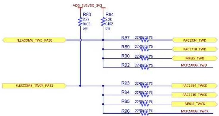
flowchart
graph TD
    A["FLEXCOM6_TWD_PA30"] --> B["R83 2.2k 0402 5%"]
    A --> C["R84 2.2k 0402 5%"]
    A --> D["R87 22B0-021% PAC1934_TWD"]
    A --> E["R89 22B0-021% PAC1710_TWD"]
    A --> F["R90 22B0-021% MBUS_TWD"]
    A --> G["R92 22B0-021% MCP23008_TWD"]
    H["FLEXCOM6_TWCK_PA31"] --> I["R93 22B0-021% PAC1934_TWCK"]
    H --> J["R94 22B0-021% PAC1710_TWCK"]
    H --> K["R95 22B0-021% MBUS_TWCK"]
    H --> L["R96 22B0-021% MCP23008_TWCK"]
The second interface is used to access the devices placed in the upper right side of the board:
• The 24AA025E48 serial EEPROM (address: 1010_011[R/W])
• The LCD or camera connected on the ISI connector
• And any device connected on the external 40-pin connector
Figure 3-18. Board Upper Right TWI Interface
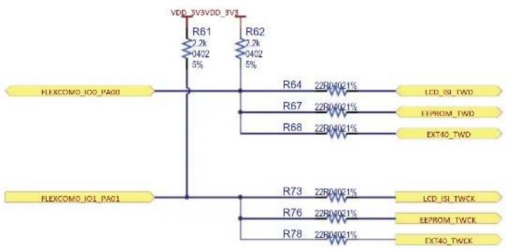
text_image
VDD_3V3VDD_3V3 R61 2.2k 0402 5% R62 2.2k 0402 5% FLEXCOMO_I00_PA00 R64 22B04021% LCD_ISI_TWD R67 22B04021% EEPROM_TWD R68 22B04021% EXT40_TWD FLEXCOMO_I01_PA01 R73 22B04021% LCD_ISI_TWCK R76 22B04021% EEPROM_TWCK R78 22B04021% EXT40_TWCK3.2.8 I/O Expander
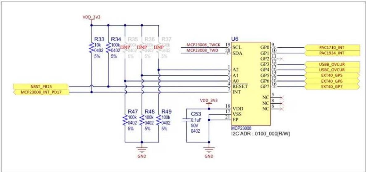
The SAM9X60-EK features an 8-bit I/O expander with serial TWI interface MCP23008.
The MCP23008 consists of multiple 8-bit configuration registers for input, output and polarity selection. The system master can enable the I/Os as either inputs or outputs by writing the I/O configuration bits.
The data for each input or output is kept in the corresponding input or output register. The polarity of the Input Port register can be inverted with the Polarity Inversion register. All registers can be read by the system master.
The interrupt output can be configured to activate under two (mutually exclusive) conditions:
- When any input state differs from its corresponding input port register state (indicating to the system master that an input state has changed)
- When an input state differs from a preconfigured register value
The Interrupt Capture register captures port values at the time of the interrupt, thereby saving the condition that caused the interrupt.
The Power-on Reset (POR) sets the registers to their default values and initializes the device state machine.
The MCP23008 communicates with the MPU via a TWI bus.
Figure 3-19. Processor IO Expander
text_image
VDD_3V3 R33 10k 100k 100k 100k 100k 100k 100k 100k 100k 100k 100k 100k 100k 100k 100k 100k 100k 100k 100k 100k 100k 1 NRST_PB25 MCP23008_INT_PD17 R47 100k 100k 100k 100k 100k 100k 100k 100k 100k 100k 100k 100k 100k 1 GND R48 100k 100k 100k 100k 100k 100k 100k 100k 100k 100k 100k 1 GND R49 100k 100k 100k 100k 100k 100k 100k 100k 100k 1 VDD_3V3 C53 5.1uF 5.2 5.3 5.4 5.5 5.6 5.7 5.8 5.9 6.0 6.1 6.2 6.3 6.4 6.5 6.6 6.7 6.8 6.9 7.0 7.1 7.2 7.3 7.4 7.5 7.6 7.7 7.8 7.9 8.0 8.1 8.2 8.3 8.4 8.5 8.6 8.7 8.8 8.9 9.0 9.1 9.2 9.3 9.4 9.5 9.6 9.7 9.8 9.9 U6 SCL GP0 SDA GP1 GP2 GP3 GP4 GP4 GP5 GP5 GP6 GP6 GP7 GP7 NC NC NC NC NC NC NC NC NC NC NC NC NC NC NC NC NC NC NC NC NC NC NC NC NC NC NC NC NC NC NC NC NC NC NC NC NC NC NC NC NC NC NC NC NC NC NC NC NC NC NC NC NC NC NC NC NC NC NC NC NC NC NC NC NC NC NC NC NC NC NC NC NC NC NC NC NC NC NC NC NC NC NC NC NC NC NC NC NC NC NC NC NC NC NC NC NC NC NC NC NC N C PAC1710_INT PAC1934_INT USBB_OVCUR USBC_OVCUR EXT40_GP5 EXT40_GP6 EXT40_GP7 I2C ADR : 0100_000[R/W]Table 3-4. I/O Expander Signal Descriptions
| PIO Signal Name Signal Description | |
| GP0 PAC1710_INT PAC1710 interrupt to MPU | |
| GP1 PAC1934_INT PAC1934 interrupt to MPU | |
| GP2 -- | |
| GP3 USBB_OVCUR USB B overcurrent indicator | |
| GP4 USBC_OVCUR USB C overcurrent indicator | |
| GP5 EXT40_GP5 Free use GPIO | |
| GP6 EXT40_GP6 Free use GPIO | |
| GP7 EXT40_GP7 Free use GPIO | |
| INT MCP23008_INT_PD17 MCP23008 Interrupt to MPU | |
| RESET - nRST | |
| SCL MCP23008_TWCK MCP23008 TWI clock | |
| SDA MCP23008_TWD MCP23008 TWI data |
3.2.9 Special Function Selectors
Some ports shared between different interfaces are separated using dedicated signal buffers to avoid any possible interference on the lines.
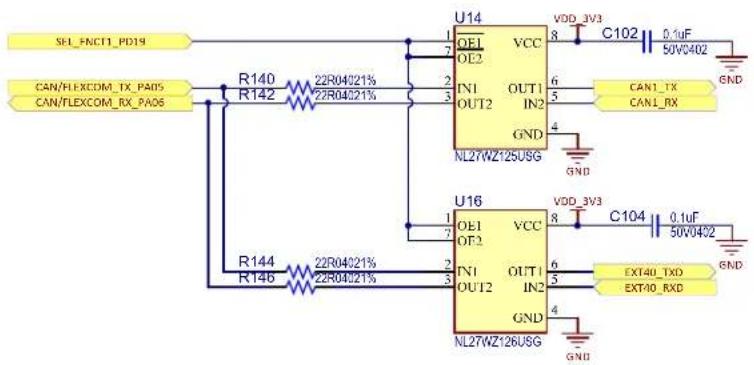
Ports PA05 and PA06 are shared between the CAN1 transceiver and a UART interface going to the 40-pin connector. The selection is done using port PD19:
• HIGH = UART to 40-pin connector
- LOW = CAN1 communication
Figure 3-20. Selection between CAN1 or EXT40 UART
text_image
SEL_ENCT1_PD19 CAN/FLEXCOM_TX_PA05 CAN/FLEXCOM_RX_PA06 R140 R142 22R04021% 22R04021% U14 OE1 VCC OE2 IN1 OUT1 OUT2 IN2 GND NL27WZ125USG VDD_3V3 8 C102 0.1uF 50V0402 CAN1_TX CAN1_RX GND R144 R146 22R04021% 22R04021% U16 OE1 VCC OE2 IN1 OUT1 OUT2 IN2 GND NL27WZ126USG VDD_3V3 8 C104 0.1uF 50V0402 EXT40_TXD EXT40_RXD GNDPorts PA09 and PA10 are shared between the CAN0 transceiver and the DEBUG UART interface going to the DEBUG connector. The selection is done using port PD20:
• HIGH = DEBUG UART communication
- LOW = CAN0 communication
Figure 3-21. Selection between CAN0 or DBGU UART

text_image
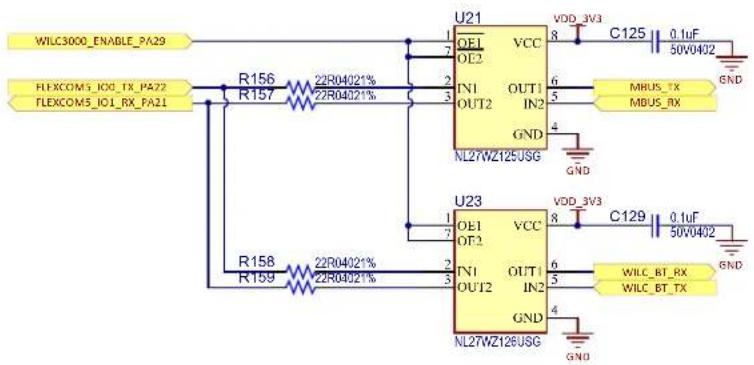
SEL_FNCT2_PD20 CAN/DBGU_TX_PA10 CAN/DBGU_RX_PA09 R141 R143 22R04021% 22R04021% R145 R147 22R04021% 22R04021% U15VDD_3V3 OEL OL2 IN1 OU12 OUT1 LN2 GND NL27WZ126USG U17 OE1 OE2 IN1 OUT1 LN2 GND NL27WZ126USG VCC 8 C103 0.1uF 50V0402 CAN0_TX CAN0_RX GND U15VDD_3V3 OEL OL2 IN1 OU12 OUT1 LN2 GND NL27WZ126USG VCC 8 C105 0.1uF 50V0402 DBGU_TX_PA10 DBGU_RX_PA09 GNDPorts PA21 and PA22 are shared between a UART interface going to the mikroBUS connector and the UART interface used to access and configure the Bluetooth functions of the ATWILC3000 module. The selection is done using port PA29:
• HIGH = ATWILC3000 UART communication
- LOW = MikroBUS CAN communication
Figure 3-22. Selection between mikroBUS UART or ATWILC3000 Bluetooth UART
text_image
WILC3000_ENABLE_PA29 FLEXCOM5_IO1_TX_PA72 FLEXCOM5_IO1_RX_PA21 R156 R157 22R04021% 22R04021% U21 OE1 OE2 VCC IN1 OUT2 IN2 GND NL27WZ125USG VDD_3V3 8 C125 0.1uF 50V0402 MRUS_TX MBUS_RX GND R158 R159 22R04021% 22R04021% U23 OE1 OE2 VCC IN1 OUT2 IN2 GND NL27WZ126USG VDD_3V3 8 C129 0.1uF 50V0402 WILC_BT_RX WILC_BT_TX GNDWhen developing an application, the designer must keep in mind to first configure the values for the selection ports (PA29, PD19 and PD20) to ensure the signal takes the desired path.
3.3 On-board Memories
The SAM9X60 features a DDR/SDR memory interface and an External Bus Interface (EBI) to enable interfacing to a wide range of external memories and to almost any type of parallel peripheral.
This section describes the memory devices mounted on the SAM9X60-EK board:
- One DDR2 SDRAM
- One NAND Flash
- One QSPI Flash
• One serial EEPROM
Additional memory can be added to the board by:
- Installing an SD or MMC card in the SD/MMC slot,
• Using the USB ports.
Support is dependent upon driver support in the OS.
3.3.1 DDR2/SDRAM
One DDR2/SDRAM (2-Gbit W972GG6KB = 16 Mwords x 16 bits x 8 banks) is used as main system memory, totaling 256 KBytes of SDRAM on the board. The memory bus is 16 bits wide and operates with a frequency of up to 200 MHz.
Figure 3-23. DDR2/SDRAM

text_image
50Ω ± 10% single-ended trace impedance Routing top or bottom 100Ω ± 10% differential trace impedance Routing top or bottom ADDR-CTL Matched Net Lengths [Tolerance = 0.25mm] Matched Net Lengths [Tolerance = 0.5mm] U10 i DDR_A2 M8 A0 DQ0 G8 DDR_D0 DDR_A3 M3 A1 DQ1 G2 DDR_D1 DDR_A4 M7 A2 DQ2 H7 DDR_D2 DDR_A5 N2 A3 DQ3 H1 DDR_D3 DDR_A6 N8 A4 DQ4 H9 DDR_D4 DDR_A7 N3 A5 DQ5 F1 DDR_D5 DDR_A8 N7 A6 DQ6 F1 DDR_D6 DDR_A9 P2 A7 DQ7 F9 DDR_D7 DDR_A10 P8 A8 LDM F3 DDR_DOM0 DDR_A11 P3 A9 LDQS_P F7 DDR_DCOS_P DIFF100 DDR_SDA10 M2 A10 LDQS_N F8 DDR_DCOS_N DIFF100 DDR_A13 P7 A11 DDR_A14 R2 A12 DDR_A15 R8 A13 DDR_A16 L2 BA0 DQ8 C8 DDR_D8 DDR_A17 L3 BA1 DQ9 C2 DDR_D9 DDR_A18 L1 BA2 DQ10 D7 DDR_D10 DDR_CKE K2 CKF DQ11 D3 DDR_D11 DDR_CLK_P DIFF100 B9 DDR_D15 DDR_CLK_N DIFF100 B3 DDR_DOM1 DDR_BAS K7 UDM B7 DDR_DOS1_P DIFF100 DDR_CAS I.7 UDS_P A8 DDR_DOS1_N DIFF100 DDR_WE K3 WE ODY GND DDR_CS I.8 CS VDDIOM R7 NC4 VDDI A1 C67 4.7uF10V0402 R3 NC3 VDDI E1 C69 0.1uF50V0402 E2 NC2 VDDI J9 C70 0.1uF50V0402 A2 NC1 VDDI M9 C71 0.1uF16V0201 A3 VSS1 VDDI R1 C81 1000pF25V0402 L3 VSS2 VDDI VDDI ODI J3 VSS3 VDDI VDDI VDDI ODI N1 VSS4 VDDI A9 C68 4.7uF10V0402 P9 VSS5 VDDI C1 C75 0.1uF50V0402 A7 VSSQ1 VDDI G3 C76 0.1uF50V0402 B2 VSSQ2 VDDI G7 C78 0.1uF16V0201 B8 VSSQ3 VDDI G9 C79 0.1uF16V0201 D2 VSSQ4 VDDI G7 C80 0.1uF16V0201 D8 VSSQ5 VDDI G9 C82 1000pF25V0402 E7 VSSQ6 VDDI VDDI ODI F2 VSSQ7 VDDL J1 C77 0.1uF50V0402 F8 VSSQ8 VDDL DDR_VREF H2 VSSQ9 VREF J2 10nF16V0402 H8 VSSQ10 VREF C64 GND J7 VSSDL W972GG6KB-25 GND3.3.2 NAND Flash
The SAM9X60-EK has native support for NAND Flash memory through its NAND Flash Controller. The board implements one MT29F4G08ABAEA 4Gb x 8 NAND Flash connected to Chip Select three (NCS3) of the microcontroller. That makes a 512-Mbyte memory space.
Figure 3-24. NAND Flash

text_image
NAND-Flash R116 R114 R115 10k 10k 10k 0402 0402 0402 5% 5% 5% VDD_3V3 NAND_CLE_PD03NAND_PD06 NAND_ALE_PD02 NAND_nRE_PD00 NAND_nWE_PD01 NAND_nC5_PD04_enabled NAND_RB_PD05 Matched Net Lengths [Tolerance = 0.25mm] U9 CLC ALE RF WL CF R/B WP NC NC NC NC NC NC NC NC NC NC NC NC NC NC NC NC NC NC NC NC NC NC NC NC NC NC NC NC NC NC NC NC NC NC NC NC NC NC NC NC NC NC NC NC NC NC NC NC NC NC NT29F4G08ABAEAWP.E TR MT29F4G08ABAEAWP.E TR NAND-Flash Matched Net Lengths [Tolerance = 0.25mm] NAND_IO1_PD07 NAND_IO2_PD08 NAND_IO3_PD09 NAND_IO4_PD10 NAND_IO5_PD11 NAND_IO6_PD12 NAND_IO7_PD13 VDD_3V3 C58 C59 C60 C61 0.1uF 0.1uF 0.1uF 0.1uF 0.1uF 0.1uF 0.1uF 0.1uF 0.1uF 0.1uF 0.1uF 0.1uF 0.1uF 0.1uF 0.1uF 0.1uF 0.1uF 0.1U2 0402 0402 0402 0402 GNDTable 3-5. NAND Flash Signal Descriptions
| PIO Signal Name Shared PIO Signal Description | ||
| PD6 NAND_IO0_PD06 – Data 0 | ||
| PD7 NAND_IO0_PD07 – Data 1 | ||
| PD8 NAND_IO0_PD08 – Data 2 | ||
| PD9 NAND_IO0_PD09 – Data 3 | ||
| PD10 NAND_IO0_PD10 – Data 4 | ||
| PD11 NAND_IO0_PD11 – Data 5 | ||
| PD12 NAND_IO0_PD12 – Data 6 | ||
| PD13 NAND_IO0_PD13 – Data 7 | ||
| PD1 NAND_nWE_PD01 – Write Enable | ||
| PD4 NAND_nCS_PD04_enabled – | Chip Select (through a Disable Boot control buffer – see 3.5.5 Disable Boot) | |
| PD2 NAND_ALE_PD02 – Address Latch Enable | ||
| PD3 NAND_CLE_PD03 – Command Latch Enable | ||
| PD0 NAND_nRE_PD00 – Output Enable | ||
| PD5 NAND_RB_PD05 – Ready/Busy# | ||
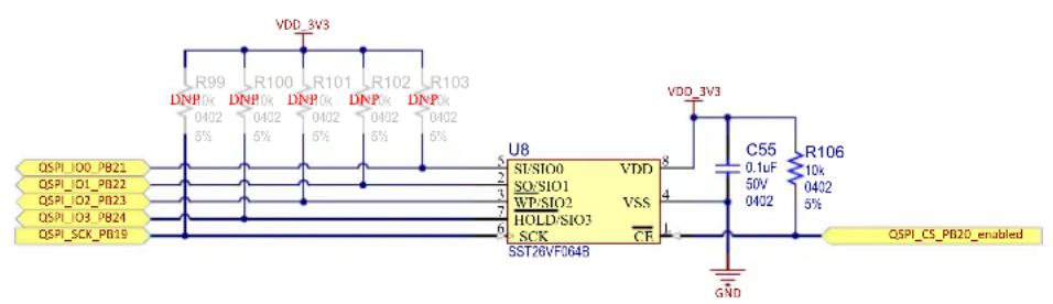
3.3.3 QSPI Serial Flash
The SAM9X60-EK board features one Quad Serial Peripheral Interface (QSPI) memory SST26VF064B.
A QSPI bus is a synchronous serial data link that provides communication with external devices in Master mode.
The QSPI can be used in SPI mode to interface with serial peripherals (such as ADCs, DACs, LCD controllers, CAN controllers and sensors), or in Serial Memory mode to interface with serial Flash memories.
The QSPI allows the system to execute code directly from a serial Flash memory (XIP, or Execute In Place, technology) without code shadowing to RAM. The Flash memory communication protocol is serial, however it is seen in the system as a conventional parallel memory (ROM, SRAM, DRAM, embedded Flash memory, etc.).
With the support of the Quad SPI protocol, the QSPI allows the system to use high-performance serial Flash memories which are small and inexpensive, instead of larger and more expensive parallel Flash memories.
Figure 3-25. QSPI Serial Flash
text_image
VDD_3V3 R99 DNP 0x 0402 5% R100 DNP 0x 0402 5% R101 DNP 0x 0402 5% R102 DNP 0x 0402 5% R103 DNP 0x 0402 5% QSPI_IO0_PB21 QSPI_IO1_PB21 QSPI_O3_PB23 QSPI_IO3_PB24 QSPI_SCK_PB19 U8 SI/SIO0 VDD SO/SIO1 VSS WP/SIO2 HOLD/SIO3 SCK CF SST26VF064B VDD_3V3 C55 0.1uF R106 50V 10k 0402 0432 5% GND QSPI_CS_PB20_enabledTable 3-6. QSPI Signal Descriptions
| PIO Signal Name Shared PIO Signal Description | |||
| PB19 | QSPI0_SCK_PB19 I2SMCC_CK QSPI Clock | ||
| PB20 | QSPI0_CS_PB20_enabled I2SMCC_WS | Chip Select (through a Disable Boot control buffer – see 3.5.5 Disable Boot) | |
| PB21 | QSPI0_IO0_PB21 I2SMCC_DIN0 Data0 | ||
| PB22 | QSPI0_IO1_PB22 I2SMCC_DOUT0 Data1 | ||
| PB23 | QSPI0_IO2_PB23 I2SMCC_MCL Data2 | ||
| PB24 | QSPI0_IO3_PB24 – Data3 | ||
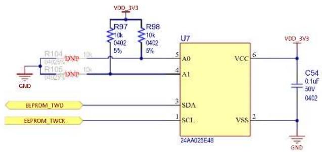
3.3.4 Serial EEPROM with Unique MAC Address
The SAM9X60-EK board embeds one Microchip 24AA025E48 serial EEPROM. The 24AA025E48 features 2048 bits of serial Electrically-Erasable Programmable Read-Only Memory (EEPROM) organized as 256 words of eight bits each and is accessed via an I²C-compatible (2-wire) serial interface. In addition, the 24AA025E48 incorporates an easy and inexpensive method to obtain a globally unique MAC or EUI address (EUI-48™). For more information about the 24AA025E48, refer to the product web page.
The EUI-48 addresses can be assigned as the actual physical address of a system hardware device or node, or it can be assigned to a software instance. These addresses are factory-programmed by Microchip and unique. They are permanently write-protected in an extended memory block located outside the standard 2-Kbit memory array.
Figure 3-26. EEPROM 24AA02E48
text_image
VDD_3V3 R97 10k 0402 R98 10k 0402 5% 5% U7 A0 VCC 6 VDD_3V3 C54 0.1uF 50V 0402 GND R104 04025% R105 04025% DNP DNP 1% 1% 4 3 SDA SCT. VSS 24AA025E48 EEPROM_TWD EEPROM_TWCKTable 3-7. EEPROM PIO Signal Descriptions
| PIO Signal | Name Shared PIO Signal Description | |
| PA00 EEPROM_TWD TWI and SPI TWI data | ||
| PA01 EEPROM_TWCK TWI and SPI TWI clock |
In the SAM9X60-EK usage context, the EEPROM device is used as a "software label" to store board information such as chip type, manufacturer name and production date, using the last two 16-byte blocks in memory. The information contained in these blocks should not be modified.
3.4 Peripherals
Several interfaces and connectors are implemented in the SAM9X60-EK with the purpose of enabling the user to test all the features that the MPU can offer and to facilitate a reference design for future customer applications.
This section describes the following peripherals mounted on the SAM9X60-EK board:
- Ethernet 10/100 port (GMAC)
- USB host/device
• Wi-Fi/Bluetooth module (optional)
• Controller Area Network (CAN) interface
• Liquid Crystal Display (LCD) interface
• Image Sensor Interface (ISI)
• Audio Class D (CLASSD) amplifier - Secure Digital Multimedia Card (SDMMC)
- mikroBUS interface
- GPIO interface
3.4.1 Ethernet 10/100 Port (GMAC)
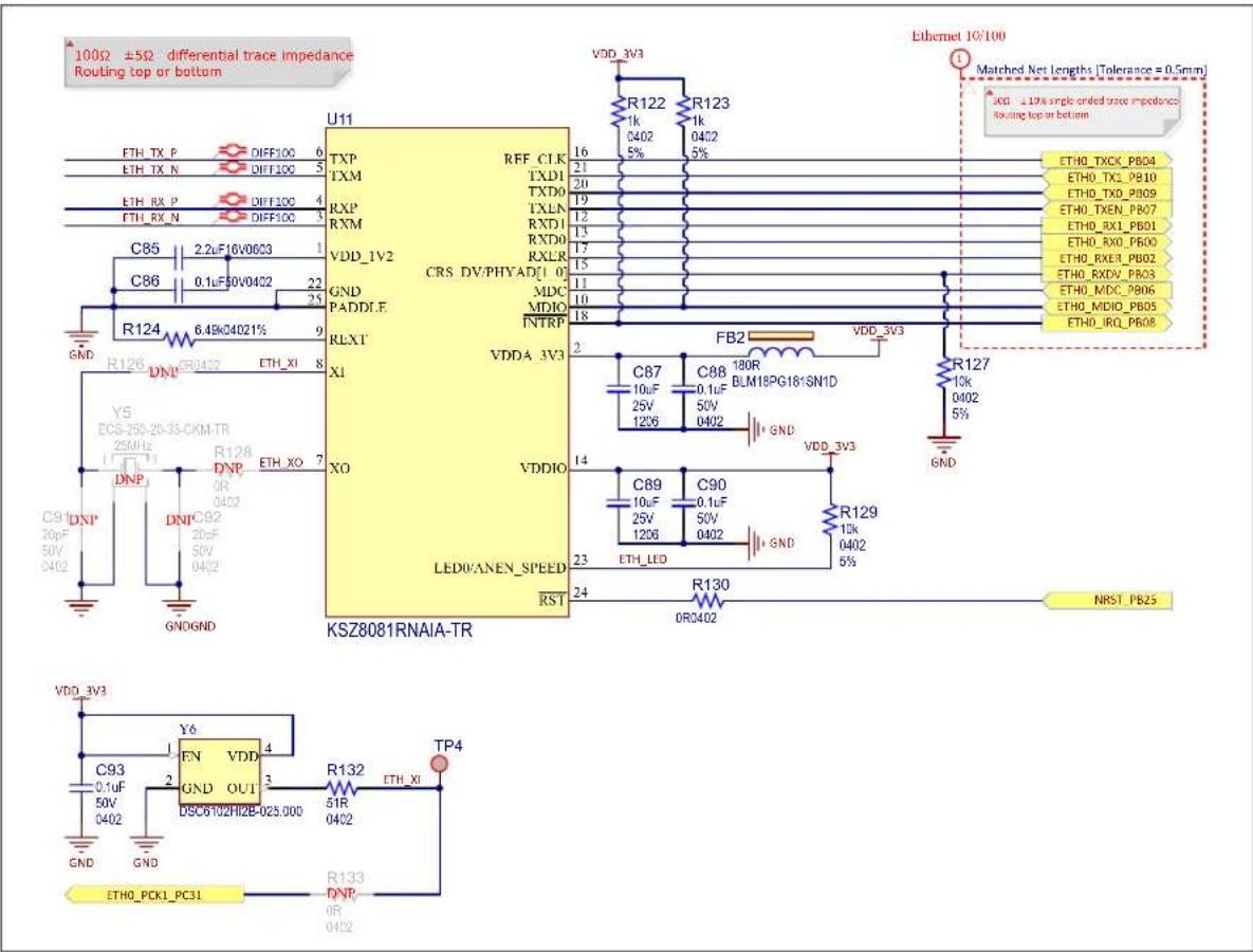
The KSZ8081 is a single-supply 10Base-T/100Base-TX Ethernet physical-layer transceiver for transmission and reception of data over standard CAT-5 unshielded twisted pair (UTP) cable. The KSZ8081 is a highly-integrated PHY solution. It reduces board cost and simplifies board layout by using on-chip termination resistors for the differential pairs and by integrating a low-noise regulator to supply the 1.2V core, and by offering 1.8/2.5/3.3V digital I/O interface support.
The KSZ8081RNA is connected over the Reduced Media Independent Interface (RMII) directly to the RMII-compliant MAC inside the SAM9X60 MPU. As the power-up default, the KSZ8081RNA uses a 25 MHz MEMS oscillator to generate all required clocks, including the 50-MHz RMII reference clock output for the MAC. For more information about the KSZ8081RNx, refer to the product web page.
An individual unique 48-bit MAC address (Ethernet hardware address) is allocated to this product and is stored in the Microchip 24AA025E48 TWI serial EEPROM described in 3.3.4 Serial EEPROM with Unique MAC Address.
Additionally, for monitoring and control purposes, a LED functionality is carried on the RJ45 connectors to indicate activity, link, and speed status.
Figure 3-27. Ethernet Interface
text_image
1002 ±5Ω differential trace impedance Routing top or bottom U11 TXP RFF_CLK TXM TXD1 TXD0 TXLN RXP RXM VDD_IV2 CRS_DV/PHYAD[1 0] GND PADDIF MDC MDIO NTRP RLXT VDDA_3V3 X1 FB2 VDD_3V3 C87 10uF C88 0.1uF BLM18PG18-SN1D 25V 50V 1206 0402 GND R127 10k 0402 5% GND Y5 ECS-250-20-35-CKM-TR 25MHz DNP R128 DNP ETH_XO 7 OR 0402 C91 DNP DNPC92 20pF 50V 0402 GNDGND XO VDDIO LED/WANEN_SPEED RST C89 10uF C90 0.1uF 50V 1206 0402 GND R129 10k 0402 5% R130 OR3402 NRST_PB25 VDD_3V3 C93 0.1uF 50V 0402 GND Y6 EN VDD 4 GND OUT 3 DSC6102HI2E-025.000 R132 ETH_XI TP4 R133 DNP OR 0402 ETHO_PCK1_PC31Table 3-8. Ethernet PHY 10/100 Signal Descriptions
| PIO Signal | Name Shared Signal Description | ||
| PB04 | ETH_TXCK_PB24 | - | Transmit clock |
| PB07 | ETH_TXEN_PB10 | - | Transmit enable |
| PB03 | ETH_RXDV_PB03 | - | Receive data valid |
| PB02 | ETH_RXER_PB02 | - | Receive error |
| PB00 | ETH_RX0_PB00 | - | Receive data 0 |
| PB01 | ETH_RX1_PB01 | - | Receive data 1 |
| PB09 | ETH_TX0_PB09 | - | Transmit data 0 |
| PB10 | ETH_TX1_PB10 | - | Transmit data 1 |
| PB06 | ETH_MDC_PB06 | - | Management data clock |
| PB05 | ETH_MDIO_PB05 | - | Management data in/out |
| PB08 | ETH_IRQ_PB08 | - | Interrupt |
Figure 3-28. Ethernet PHY Connector
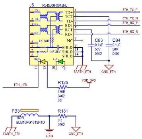
text_image
J5 RJMSJ00-0045NL 1 TX 2 TX 3 RX 4 RX 5 RX 6 RX 7 4X 76R 8 1.0F 2kV SHLD 9 1.0F 2kV SHLD 10 1.0F 2kV SHLD 11 1.0F 2kV SHLD 12 1.0F 2kV SHLD 13 1.0F 2kV SHLD 14 1.0F 2kV SHLD 15 1.0F 2kV SHLD 16 1.0F 2kV SHLD 17 1.0F 2kV SHLD 18 1.0F 2kV SHLD 19 1.0F 2kV SHLD 20 1.0F 2kV SHLD 21 1.0F 2kV SHLD 22 1.0F 2kV SHLD 23 1.0F 2kV SHLD 24 1.0F 2kV SHLD 25 1.0F 2kV SHLD 26 1.0F 2kV SHLD 27 1.0F 2kV SHLD 28 1.0F 2kV SHLD 29 1.0F 2kV SHLD 30 1.0F 2kV SHLD 31 1.0F 2kV SHLD 32 1.0F 2kV SHLD 33 1.0F 2kV SHLD 34 1.0F 2kV SHLD 35 1.0F 2kV SHLD 36 1.0F 2kV SHLD 37 1.0F 2kV SHLD 38 1.0F 2kV SHLD 39 1.0F 2kV SHLD 40 1.0F 2kV SHLD 41 1.0F 2kV SHLD 42 1.0F 2kV SHLD 43 1.0F 2kV SHLD 44 1.0F 2kV SHLD 45 1.0F 2kV SHLD 46 1.0F 2kV SHLD 47 1.0F 2kV SHLD 48 1.0F 2kV SHLD 49 1.0F 2kV SHLD 50 1.0F 2kV SHLD 51 1.0F 2kV SHLD 52 1.0F 2kV SHLD 53 1.0F 2kV SHLD 54 1.0F 2kV SHLD 55 1.0F 2kV SHLD 56 1.0F 2kV SHLD 57 1.0F 2kV SHLD 58 1.0F 2kV SHLD 59 1.0F 2kV SHLD 60 1.0F 2kV SHLD 61 1.0F 2kV SHLD 62 1.0F 2kV SHLD 63 1.0F 2kV SHLD 64 1.0F 2kV SHLD 65 1.0F 2kV SHLD 66 1.0F 2kV SHLD 67 1.0F 2kV SHLD 68 1.0F 2kV SHLD 69 1.0F 2kV SHLD 70 1.0F 2kV SHLD 71 1.0F 2kV SHLD 72 1.0F 2kV SHLD 73 1.0F 2kV SHLD 74 1.0F 2kV SHLD 75 1.0F 2kV SHLD 76 1.0F 2kV SHLD 77 1.0F 2kV SHLD 78 1.0F 2kV SHLD 79 1.0F 2kV SHLD 80 1.0F 2kV SHLD 81 1.0F 2kV SHLD 82 1.0F 2kV SHLD 83 1.0F 2kV SHLD 84 1.0F 2kV SHLD 85 1.0F 2kV SHLD 86 1.0F 2kV SHLD 87 1.0F 2kV SHLD 88 1.0F 2kV SHLD 89 1.0F 2kV SHLD 90 1.0F 2kV SHLD 91 1.0F 2kV SHLD 92 1.0F 2kV SHLD 93 1.0F 2kV SHLD 94 1.0F 2kV SHLD 95 1.0F 2kV SHLD 96 1.0F 2kV SHLD 97 1.0F 2kV SHLD 98 1.0F 2kV SHLD 99 1.0F 2kV SHLD 100 EARTH_ETH GND_ETH VDD_3V3 FB3 R131 R138 BLM18PG18ISNID OR GND GND_ETH ETH_TX_P ETH_TX_N ETH_RX_P ETH_RX_N C83 C84 C84 C84 C84 C84 C84 C84 C84 C84 C84 C84 C84 C84 C84 C84 C84 C84 C84 C84 C84 C84 C84 C84 C84 C84 C84 C84 C84 C84 C84 C84 C84 C84 C84 DRLBMLMELGALDINHOLIYHOLIYHOLIYHOLIYHOLIYHOLIYHOLIYHOLIYHOLIYHOLIYHOLIYHOLIYHOLIYHOLIYHOLIYHOLIYHOLIYHOLIYHOLIYHOLIYHOLIYHOLIYHOLIYHOLIYHOLIYHOLI YHOLIYHOLIYHOLIYHOLIYHOLIYHOLIYHOLIYHOLIYHOLIYHOLIYHOLIYHOLIYHOLIYHOLIYHOLIYHOLIYHOLIYHOLIYHOLIYHOLIYHOLIYHOLIYHOLIYHOLIYHOLIYS HOLDING INCHANGES IN CHANGES IN CHANGES IN CHANGES IN CHANGES IN CHANGES IN CHANGES IN CHANGES IN CHANGES IN CHANGES IN CHANGES IN CHANGES IN CHANGES IN CHANGES IN CHANGES IN CHANGES IN CHANGES IN CHANGES IN CHANGES IN CHANGES IN CHANGES IN CHANGES IN CHANGES IN CHANGES IN CHANGES IN CHANGES IN CHANGES IN CHANGES IN CHANGES IN CHANGES IN CHANGES IN CHANGES IN CHANGES IN CHANGES IN CHanges IN CHanges IN CHanges IN CHanges IN CHanges IN CHanges IN CHanges IN CHanges IN CHanges IN CHanges IN CHanges IN CHanges IN CHanges IN CHanges IN CHanges IN CHanges IN CHanges IN CHanges IN CHanges IN CHanges IN CHanges IN CHanges IN CHanges IN CHanges IN CHanges IN CHanges IN CHanges IN CHanges IN CHanges IN CHanges IN CHanges IN CHanges IN CHanges IN CHangesINCHANGES IN CHANGES IN CHANGES IN CHANGES IN CHANGES IN CHANGES IN CHANGES IN CHANGES IN CHANGES IN CHANGES IN CHANGES IN CHANGES IN CHANGES IN CHANGES IN CHANGES IN CHANGES IN CHANGES IN CHANGES IN CHANGES IN CHANGES IN CHANGES IN CHANGES IN CHANGES IN CHANGES IN CHANGES IN CHANGES IN CHANGES IN CHANGES IN CHANGES IN CHANGES IN CHANGES IN CHANGES IN CHANGESINCHANGESINCHANGESINCHANGESINCHANGESINCHANGESINCHANGESINCHANGESINCHANGESINCHANGESINCHANGESINCHANGESINCHANGESINCHANGESINCHANGESINCHANGESINCHANGESINCHANGESINCHANGESINCHANGESINCHANGESINCHANGESINCHANGESINCHANGESINCHANGESINCHANGESINCHANGESINCHANGESINCHANGESINCHANGESINCHANGESINCHANGESINCHANGESINCHANGESINCHometersTable 3-9. Ethernet RJ45 Connector J5 Pin Assignment
| Pin No Signal Name Signal Description | ||
| 1 TD+ Transmit | ||
| 2 TD- Transmit | ||
| 3 RD+ Receive | ||
| 4 Decoupling capacitor – | ||
| 5 Decoupling capacitor – | ||
| 6 RD- Receive | ||
| 7 NC – | ||
| 8 EARTH / GND Common ground | ||
| 9 ACT LED LED activity | ||
| 10 ACT LED LED activity | ||
| 11 LINK LED | LED link connection | |
| 12 LINK LED | LED link connection | |
| 13 EARTH / GND Common ground | ||
| 14 EARTH / GND Common ground | ||
| 15 NC – | ||
| 16 NC – | ||
3.4.2 USB Host/Device
The USB (Universal Serial Bus) is a hot-pluggable general-purpose high-speed I/O standard for computer peripherals. The standard defines connector types, cabling, and communication protocols for interconnecting a wide variety of electronic devices. The USB 2.0 Specification defines data transfer rates as high as 480 Mbps (also known as High Speed USB). A USB host bus connector uses four pins: a power supply pin (5V), a differential pair (D+ and D- pins) and a ground pin.
The SAM9X60-EK board features three USB communication ports named USB-A to USB-C ^™ .
The USB-A port can act only as a USB device interface and can be accessed via the USB Micro-B connector (J7).
Two resistors are placed on its power rail to form a voltage divider, converting 5V into 3.3V that is then used to signal the presence of a USB host to the MPU.
In the case of board bring-up, USB-A is the default port used to connect to the MPU over SAM-BA (SAM Boot Assistance). For more information, refer to the product web page.
The USB-A port is also used as a secondary power source, as mentioned in 3.1 Power Supply Topology and Power Distribution. In most cases, this port is limited to 500 mA.
Figure 3-29. USB-A Port

text_image
V_BUS_USBA USBA_VBUS_5V C106 20pF 50V 0402 R148 100k 0402 5% R150 200k 0402 1% USBA_VBUSDETECT_PB16 J7 V_BUS D- D+ TD GND USBA_N USBA_P DIFF90 DIFF90 USBA_N USBA_P FB5 180R EARTH_USB_A 90Ω ±15% differential trace impedance Routing top or bottomTable 3-10. USB-A Connector Signal Descriptions
| Pin No Signal Name Signal Description | |
| 1 USBA_VBUS_5V First port 5V power | |
| 2 USBA_N First port data minus | |
| 3 USBA_P First port data plus | |
| 4 ID – (not used) | |
| 5 GND First port ground |
Table 3-11. USB-A PIO Signal Descriptions
| PIO Signal | Name Shared Signal Description | ||
| PB16 | USBA_VBUSDETECT_PB16 | — | VBUS detection |
The USB-B and USB-C ports are connected to the stacked USB Type-A connector (J8) and each port can act both as device and as host.
Figure 3-30. USB-B and USB-C Ports
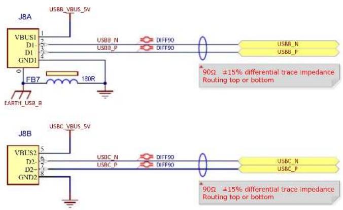
text_image
J8A VBUS1 D1- GND1 FB7 130R EARTH_USB_B J8B VBUS2 D2- GND2 USBB_VBUS_5V USB8_N DIFF90 USB8_P DIFF90 USBB_N USBB_P 90Ω ±15% differential trace impedance Routing top or bottom USBC_VBUS_5V USBC_N DIFF90 USBC_P DIFF90 USBC_N USBC_P 90Ω ±15% differential trace impedance Routing top or bottomTable 3-12. USB-B and USB-C Connector Signal Descriptions
| Pin No Signal Name Signal Description | |
| 0 EARTH_USB_B Connector chassis connected to ground | |
| 1 USBB_VBUS_5V Second port 5V power | |
| 2 USBB_N Second port data minus | |
| 3 USBB_P Second port data plus | |
| 4 GND Second port ground | |
| 5 USBC_VBUS_5V Third port 5V power | |
| 6 USBC_N Third port data minus | |
| 7 USBC_P Third port data plus | |
| 8 GND Third port ground | |
In Host mode, the USB Host ports B and C are equipped with 500-mA high-side power switches to enable self-powered and bus-powered applications. The USBx_EN_5V_PDxx signal controls the current limiting power switch MIC2025, which in turn supplies power to a client device. Per the USB specification, bus-powered USB 2.0 devices are limited to a maximum of 500 mA, therefore the MIC2025 limits the current and indicates an overcurrent with the USBx_OVCUR signal. For more information about the MIC2025, refer to the product web page.
Figure 3-31. USB Power Switches

text_image
VDD_MAIN_5V U19 EN IN GND NC MIC2025-1YM USB Power Switch R152 10k 0402 5% FB6 C113 10uF 25V 120S USBB_OVCUR VDD_3V3 V_BUS_USBB C114 10uF 25V 120S C115 0.1uF 50V 0402 C116 100μF 16V Radial, Can USBB_VBUS_5V VDD_MAIN_5V U20 EN IN GND NC MIC2025-1YM USB Power Switch R154 10k 0402 5% FB8 C119 10uF 25V 120S USBC_VBUS_5V V_BUS_USBC C120 10uF 25V 120S C121 0.1uF 50V 0402 C122 100μF 16V Radial, CanTable 3-13. USB Power Switch PIO Signal Descriptions
| PIO Signal Name Shared Signal Description | ||
| PD14 USBA_EN_5V_PD14 – Power switch enable (active high) | ||
| GP2 expander USBA_OVCUR – Indicates overcurrent (open drain) | ||
| PD15 USBA_EN_5V_PD15 – Power switch enable (active high) | ||
| GP3 expander USBB_OVCUR – Indicates overcurrent (open drain) | ||
| PD16 USBC_EN_5V_PD16 – Power switch enable (active high) | ||
| GP4 expander USBC_OVCUR – Indicates overcurrent (open drain) |
3.4.3 Wi-Fi/Bluetooth Module (Optional)
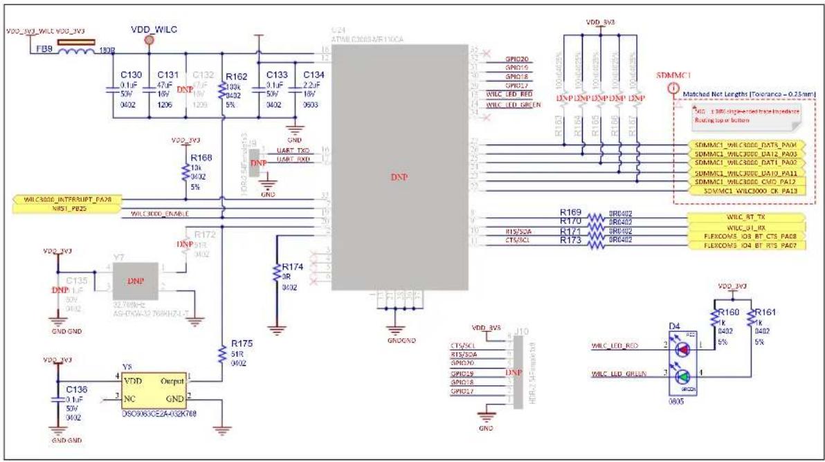
The user has the option to solder an ATWILC3000-MR110CA Wi-Fi/BT module with a chip antenna.
The ATWILC3000-MR110PA WLAN PHY is designed to achieve a reliable and power-efficient physical layer communication as specified by IEEE ^ 802.11 b/g/n in Single Stream mode with a 20-MHz bandwidth. Advanced algorithms are used to achieve maximum throughput in a real-world communication environment with impairments and interference. The PHY implements all required functions such as FFT, filtering, FEC (Viterbi decoder), frequency and timing acquisition and tracking, channel estimation and equalization, carrier sensing and clear channel assessment, as well as automatic gain control. The module is available in a fully certified, 22.428 x 17.732 mm, 36-pin module package. For more information about the ATWILC3000, refer to the product web page.
Figure 3-32. Wi-Fi/Bluetooth Interface
text_image
VDD_W3_WILC_VDD_W3 FB8 180Ω VDD_WILC C130 0.1μF 50V 3402 C131 47μF 16V 1206 DNP C132 7μF 18V 1209 R162 100k 4032 5% C133 0.1μF 50V 3402 C134 2.2μF 18V 9033 GND VDD_BV3 R166 13k 4032 5% UART TXO UART RXD GND WILC3000_INTERSHIFT_FA28 NIST_PB25 WILC3000_ENABLE DNP R172 DNP 51R 3402 R174 5R 3402 DNP VDD_BV3 C135 DNP 37V 3402 GND_GND VDD_BV3 C136 0.1μF 50V 3402 Y8 VDD_Output NC GND OSC0X6CE2A-032K700 GND_GND DNP R175 51R 3402 GND_GND ATMIL C3003/VE10CA SPID26 SPID15 SPID18 SPID17 WILC_LED_RED WILC_LED_GREEN R169 R170 R171 R173 BRG402 BRG403 BRG402 BRG402 SDMMC1 Matched Net Lengths [Tolerance - 0.25mm] GND_1.1MHz single-ended max power supplies. Routing top or bottom SDMMC1_WILC3000_DAT1x_PA0V SDMMC1_WILC3000_DAT2x_PA0S SDMMC1_WILC3000_DAT1x_PA0Z SDMMC1_WILC3000_DAT2x_PA1I SDMMC1_WILC3000_CMDx_PA12 SDMMC1_WILC3000_CKx_PA13 WILC_BT_TX WILC_bL_RX FLEXCOVS_IOB_BT_CTS_PA0B FLEXCOVS_IO4_BT_RTS_PA07Table 3-14. Wi-Fi/Bluetooth Signal Descriptions
| PIO Signal Name Shared Signal Description | |||
| PA11 SDMMC1_WILC3000_DAT0_PA11 | - | SDIO data | |
| PA02 | SDMMC1_WILC3000_DAT1_PA02 | - | SDIO data |
| PA03 | SDMMC1_WILC3000_DAT2_PA03 | - | SDIO data |
| PA04 | SDMMC1_WILC3000_DAT3_PA04 | - | SDIO data |
| PA12 | SDMMC1_WILC3000_CMD_PA12 | - | SDIO command |
| PA13 | SDMMC1_WILC3000_CK_PA13 | - | SDIO clock |
| PA21 | FLEXCOM1_IO1_RX_PA21 | - | Bluetooth serial TX (RX into SAM9X60) |
| PA22 | FLEXCOM1_IO0_TX_PA22 | - | Bluetooth serial RX (TX from SAM9X60) |
| PA07 | FLEXCOM1_IO1_RTS_PA07 | - | Bluetooth serial RTS |
| PA08 | FLEXCOM1_IO1_CTS_PA08 | - | Bluetooth serial CTS |
| PB25 | NRST_PB25 | - | Module reset |
| PA28 | WILC3000_INTERUPT_PA28 | - | Interrupt |
| PA29 | WILC3000_ENABLE_PA29 | - | Chip enable |
Special care must be taken when powering the ATWILC3000 wireless module. Due to the nature of the wireless transmission, the module draws a lot of current from its supply rail. In the worst-case scenario, the module can draw up to 300 mA. The main PMIC on the board, the MIC2800, has a maximum output capacity of 300 mA on its 3.3V rail, therefore it is not fit to power this module alongside the other components on the board.
To address this issue, the module is fitted with its own separate power supply, the MCP1725, which is a 500-mA Low Dropout (LDO) linear regulator that provides high current and low output voltages in a very small package. For more information about the MCP1725, refer to the product web page.
The MCP1725 was chosen because it can supply the current required by the module, and because it features a shutdown input pin (SHDN) and a Power Good output pin (PWRGD):
- The SHDN input allows to shut down the wireless module if it is unused, therefore saving power.
- The PWRGD output ensures that the ATWILC3000 wireless module is kept in reset until its power rails are stable.
Figure 3-33. Wi-Fi/Bluetooth Enable
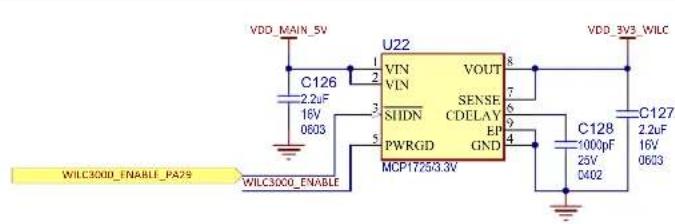
text_image
VDD_MAIN_5V U22 VOUT 8 VDD_3V3_WILC C126 2.2uF 16V 0603 VIN VIN SENSE CDELAY EP GND SIIDN PWRGD MCP17253.3V 9 4 C128 1000pF 25V C402 C127 2.2uF 16V 0603 WILC300D_ENABLE_PA29 WILC300D_ENABLENote: Enabling the ATWILC3000 module prevents the Flexcom UART from being used with the mikroBUS connector (this is switched by U23).
3.4.4 Controller Area Network (CAN) Interface
Two MCP2542 transceivers are placed on the SAM9X60-EK.
The MCP2542 is a high-speed CAN transceiver that provides the interface between the Controller Area Network (CAN) protocol controller and the physical two-wire bus. For more information about the MCP2542, refer to the product web page.
Figure 3-34. Dual CAN Interface
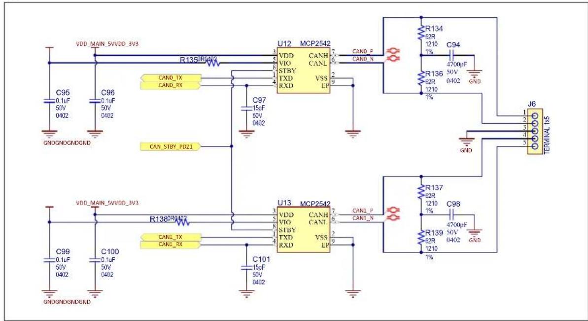
text_image
VDD_MAIN_5VVDD_3V3 R1359R0402 C95 0.1uF 50V 0402 C96 0.1uF 50V 0402 CAN_TX CAN_RX CAN_STBY_PD21 U12 MCP2542 VDD CANH VIO CANL STBY VSS TXD EP RXD CAN0_P CAN0_N C97 15pF 50V 0402 U13 MCP2542 VDD CANH VIO CANL STBY VSS TXD EP RXD EP CAN1_P CAN1_N C101 15pF 50V 0402 C100 0.1uF 50V 0402 C99 0.1uF 50V 0402 U13 62R 1210 C94 1% R136 62R 1210 4700pF 50V GND GND J6 TERMINAL 1x5 R137 62R 1210 C98 1% R139 62R 1210 4700pF 50V GNDTable 3-15. CAN Signal Descriptions
| PIO Signal Name Shared Signal Description | ||
| PD21 CAN_STBY_PD21 – Dual CAN standby | ||
| PA10 CAN0_TX_PA10 – CAN transmit port 0 | ||
| PA09 CAN0_RX_PA09 – CAN receive port 0 | ||
| PA05 CAN1_TX_PA05 – CAN transmit port 1 | ||
| PA06 CAN1_RX_PA06 – CAN receive port 1 |
Table 3-16. CAN Connector J6 Signal Description
| Pin No Signal Name | Signal Description | |
| 1 CANH Differential positive port 0 | ||
| 2 CANL Differential negative port 0 | ||
| 3 GND Common ground | ||
| 4 CANH Differential positive port 1 | ||
| 5 CANL Differential negative port 1 | ||
CAN1 function and UART on the external 40-pin connector are shared and selectable through the SEL_FNCT1_PD19 PIO.
CAN0 function and Debug UART are shared and selectable through the SEL_FNCT2_PD20 PIO.
3.4.5 Liquid Crystal Display (LCD) Interface
The SAM9X60-EK board provides a connector with 24 bits of data and control signals to the LCD interface.
Optional displays such as AC320005-5 (refer to the product web page) can be connected to the board.
In order to operate correctly with various LCD modules, two voltage lines are available: 3.3V and 5VDC (default). The selection is made with 0R resistors.
J15 is a 1.27-mm pitch, 50-pin header. It gives access to the LCD signals.
Figure 3-35. LCD Connector

text_image
Matched Net Lengths [Tolerance = 0.5mm] LCD LCD_ID_PD14 LCD_D0_ISI_D0_PC00 LCD_D1_ISI_D1_PC01 LCD_D2_ISI_D2_PC02 LCD_D3_ISI_D3_PC03 LCD_D4_ISI_D4_PC04 LCD_D5_ISI_D5_PC05 LCD_D6_ISI_D6_PC06 LCD_D7_ISI_D7_PC07 LCD_D8_ISI_D8_PC08 LCD_D9_ISI_D9_PC09 LCD_D10_ISI_D10_PC10 LCD_D11_ISI_D11_PC11 LCD_D12_ISI_PCK_PC12 LCD_D13_ISI_VSYNC_PC13 LCD_D14_ISI_HSYNC_PC14 LCD_D15_ISI_MCK_PC15 LCD_D16_ISI_nRST_PC16 LCD_D17_PC17 LCD_D18_PC18 LCD_D19_PC19 LCD_D20_PC20 LCD_D21_PC21 LCD_D22_PC22 LCD_D23_PC23 LCD_PCLK_PC30 LCD_VSYNC/CS_PC27 LCD_HSYNC/WE_PC28 LCD_DATA_ENABLE_PC29 LCD_ISI_ENABLE_PC24 LCD_IRQ1_PC25 LCD_PWM_PC26 VDD_MAIN_SV VDD_3V3 OR0402 R214 OR0402 R217 MNT GND J15 FFC/IFPC 50P FemaleTable 3-17. LCD Connector J15 Signal Descriptions
| Pin No | LCD pin PIO Signal Function | |||
| 1 ID | PD18 | LCDID_PD18 | ID LCD module | |
| 2 GND – GND Ground | ||||
| 3 LCDDAT0 | PC0 | LCD_D0_ISI_D0_PC00 | Data line | |
| 4 LCDDAT1 | PC1 | LCD_D1_ISI_D1_PC01 | Data line | |
| 5 LCDDAT2 | PC2 | LCD_D2_ISI_D2_PC02 | Data line | |
| 6 LCDDAT3 | PC3 | LCD_D3_ISI_D3_PC03 | Data line | |
| 7 GND – GND Ground | ||||
| 8 LCDDAT4 | PC4 | LCD_D4_ISI_D4_PC04 | Data line | |
| 9 LCDDAT5 | PC5 | LCD_D5_ISI_D5_PC05 | Data line | |
| 10 | LCDDAT6 | PC6 | LCD_D6_ISI_D6_PC06 | Data line |
| 11 | LCDDAT7 | PC7 | LCD_D7_ISI_D7_PC07 | Data line |
| 12 | GND – GND Ground | |||
| 13 | LCDDAT8 | PC8 | LCD_D8_ISI_D8_PC08 | Data line |
| 14 | LCDDAT9 PC9 LCD_D9_ISI_D9_PC09 Data line | |||
| 15 | LCDDAT10 PC10 LCD_D10_ISI_D10_PC10 Data line | |||
| 16 | LCDDAT11 PC11 LCD_D11_ISI_D11_PC11 Data line | |||
| 17 | GND - GND | Ground | ||
| 18 | LCDDAT12 PC12 LCD_D12_ISI_PCK_PC12 Data line | |||
| 19 | LCDDAT13 PC13 LCD_D13_ISI_VSYNC_PC13 Data line | |||
| 20 | LCDDAT14 PC14 LCD_D14_ISI_HSYNC_PC14 Data line | |||
| 21 | LCDDAT15 PC15 LCD_D15_ISI_MCK_PC15 Data line | |||
| 22 | GND - GND | Ground | ||
| 23 | LCDDAT16 PC16 LCD_D16_PC16 Data line | |||
| 24 | LCDDAT17 PC17 LCD_D17_PC17 Data line | |||
| 25 | LCDDAT18 PC18 LCD_D18_PC18 Data line | |||
| 26 | LCDDAT19 PC19 LCD_D19_PC19 Data line | |||
| 27 | GND - GND | Ground | ||
| 28 | LCDDAT20 PC20 LCD_D20_PC20 Data line | |||
| 29 | LCDDAT21 PC21 LCD_D21_PC21 Data line | |||
| 30 | LCDDAT22 PC22 LCD_D22_PC22 Data line | |||
| 31 | LCDDAT23 PC23 LCD_D23_PC23 Data line | |||
| 32 | GND - GND | Ground | ||
| 33 | LCDPCK PC30 LCD_PCLK_PC30 Pixel clock | |||
| 34 | LCDVSYNC PC27 LCD_VSYNC/CS_PC27 Vertical synchronization | |||
| 35 | LCDHSYNC PC28 LCD_HSYNC/WE_PC28 Horizontal synchronization | |||
| 36 | LCDDEN PC29 LCD_DATA_ENABLE_PC29 Data enable | |||
| 37 | SPI_SPCK - NC | Test point to access the SPI interface via DNP resistor (see Figure 3-35) | ||
| 38 | SPI_MOSI - NC | Test point to access the SPI interface via DNP resistor (see Figure 3-35) | ||
| 39 | SPI_MISO - NC | Test point to access the SPI interface via DNP resistor (see Figure 3-35) | ||
| 40 | SPI_NPCS0 - NC Test point to access the SPI interface via DNP resistor (see Figure 3-35) | |||
| 41 | LCDDISP PC24 LCD_ISI_ENABLE_PC24 Display enable signal | |||
| 42 | TWD PA00 LCD_TWD I ^2C data line (maXTouch) | |||
| 43 | TWCK PA01 LCD_TWCK I ^2C clock line (maXTouch) | |||
| 44 | GPIO PC25 LCD_IRQ1_PC25 maXTouch interrupt line | |||
| 45 | GPIO PB17 LCD_IRQ2_PB17 Interrupt line for other I ^2C devices | |||
| ......continued | |||
| Pin No | LCD pin | PIO Signal Function | |
| 46 | LCDPWM PC26 | LCD_PWM_PC26 Backlight control | |
| 47 | RESET PB25 | NRST_PB25 Reset for both display and maXTouch | |
| 48 | Main_5V/3.3V | VCC VCC 3.3V or 5V supply (0R) | |
| 49 | Main_5V/3.3V | VCC VCC 3.3V or 5V supply (0R) | |
| 50 | GND _ GND Ground | ||
3.4.6 Image Sensor Interface (ISI)
The SAM9X60-EK board provides a connector (J17) for connecting a 12-bit external camera. A TWI connection is also included for controlling the camera.

The ISI interface and LCD interface are mutually exclusive and should be used one at a time.
J17 is a 30-pin, 2.54-mm pitch header. It gives access to the ISI signals.
Figure 3-36. ISI Expansion Header
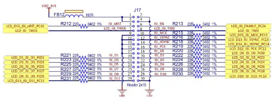
text_image
VDD_3V3 FB12 180R J17 LCD_D16_ISI_nRST_PC16 R212 22R 0402 1% ISI_nRST 5 6 ISI_EN R213 22R 0402 1% LCD_ISI_FNABLE_PC24 LCD_ISI_TWCK LCD_ISI_TWCK LCD_ISI_TWCK LCD_ISI_TWD LCD_ISI_TWD LCD_D1_ISI_D1_PCD1 R221 22R 0402 1% ISI_D1 19 20 ISI_MCK R215 22R 0402 1% LCD_D15_ISI_MCK_PC15 LCD_D3_ISI_D3_PCD3 R223 22R 0402 1% ISI_D3 21 22 ISI_VSYNC R216 22R 0402 1% LCD_D13_ISI_VSYNC_PC13 LCD_D5_ISI_D5_PCD5 R225 22R 0402 1% ISI_D5 23 24 ISI_HSYNC R218 22R 0402 1% LCD_D14_ISI_HSYNC_PC14 LCD_D7_ISI_D7_PCD7 R227 22R 0402 1% ISI_D7 25 26 ISI_PCK R219 22R 0402 1% LCD_D12_ISI_PCK_PC12 LCD_D9_ISI_D9_PCD9 R229 22R 0402 1% ISI_D9 27 28 ISI_D0 R220 22R 0402 1% LCD_D0_ISI_D0_PCD0 LCD_D11_ISI_D11_PC11 R231 22R 0402 1% ISI_D11 29 30 Header 2x15 LCD DIO GND GND LCD_D0_GND PC00 LCD_D1_SI_D1_PCD1 R233 22R 0402 1% ISI_D3 21 22 ISI_D4 R224 22R 0402 1% LCD_D2_ISI_D3_PCD2 LCD_D3_ISI_D3_PCD3 R235 22R 0402 1% ISI_D5 23 24 ISI_D6 R226 22R 0402 1% LCD_D4_ISI_D4_PCD4 LCD_D5_ISI_D5_PCD5 R237 22R 0402 1% ISI_D7 25 26 ISI_D8 R228 22R 0402 1% LCD_D6_ISI_D6_PCD6 LCD_D7_ISI_D7_PCD7 R239 22R 0402 1% ISI_D9 27 28 ISI_D10 R230 22R 0402 1% LCD_D8_ISI_D8_PCD8 LCD_D9_ISI_D9_PCD9 R241 22R 0402 1% ISI_D11 29 LCD_D11_ISI_D11_PC11Table 3-18. ISI Connector J17 Signal Descriptions
| Pin No | ISI Pin | PIO | Signal | Function |
| 1 | Main_3V3 | VCC | VCC | 3.3V supply |
| 2 | GND | - GND | Ground | |
| 3 | Main_3V3 | VCC | VCC | 3.3V supply |
| 4 | GND | - GND | Ground | |
| 5 | ISI_nRST | PC16 | LCD_RESET_PC16 | Camera reset line |
| 6 | ISI_EN | PC24 | LCD_ISI_ENABLE_PC24 | Camera enable |
| 7 | ISI_TWCK | PA00 | LCD_TCKD | TWI interface clock line |
| 8 | ISI_TWD | PA01 | LCD_TWD | TWI interface data line |
| 9 | GND | - GND | Ground | |
| 10 | ISI_MCK | PC15 | LCD_D15_ISI_MCK_PC15 | Master clock line |
| 11 | GND | - | GND | Ground |
| ......continued | ||||
| Pin No ISI | Pin PIO Signal Function | |||
| 12 ISI_VSYNC PC13 LCD_D13_ISI_VSYNC_PC13 Vertical synchronization | ||||
| 13 GND – | GND Ground | |||
| 14 ISI_HSYNC PC14 LCD_D14_ISI_HSYNC_PC14 Horizontal synchronization | ||||
| 15 GND – | GND Ground | |||
| 16 ISI_PCK PC12 LCD_D12_ISI_PCK_PC12 Clock line | ||||
| 17 GND – | GND Ground | |||
| 18 ISI_D0 | PC00 LCD_D0_ISI_D0_PC00 | Data line | ||
| 19 ISI_D1 | PC01 LCD_D1_ISI_D1_PC01 | Data line | ||
| 20 ISI_D2 | PC02 LCD_D2_ISI_D2_PC02 | Data line | ||
| 21 ISI_D3 | PC03 LCD_D3_ISI_D3_PC03 | Data line | ||
| 22 ISI_D4 | PC04 LCD_D4_ISI_D4_PC04 | Data line | ||
| 23 ISI_D5 | PC05 LCD_D5_ISI_D5_PC05 | Data line | ||
| 24 ISI_D6 | PC06 LCD_D6_ISI_D6_PC06 | Data line | ||
| 25 ISI_D7 | PC07 LCD_D7_ISI_D7_PC07 | Data line | ||
| 26 ISI_D8 | PC08 LCD_D8_ISI_D8_PC08 | Data line | ||
| 27 ISI_D9 | PC09 LCD_D9_ISI_D9_PC09 | Data line | ||
| 28 ISI_D10 | PC10 LCD_D10_ISI_D10_PC10 | Data line | ||
| 29 | ISI_D11 | PC11 | LCD_D11_ISI_D11_PC11 | Data line |
| 30 GND – | GND Ground | |||
3.4.7 Audio Class D (CLASSD) Amplifier
The Audio Class D (CLASSD) Amplifier is a digital input, Pulse Width Modulated (PWM) output stereo Class D amplifier. CLASSD features a high-quality interpolation filter embedding a digitally-controlled gain, an equalizer and a de-emphasis filter.
On its input side, CLASSD is compatible with most common audio data rates. On the output side, its PWM output can drive either:
- high-impedance single-ended or differential output loads (Audio DAC application), or
• external MOSFETs through an integrated non-overlapping circuit (Class D power amplifier application).
For more information, refer to the SAM9X60 datasheet (see 1.2 Recommended Reading).
The output stage of the CLASSD amplifier featured on the SAM9X60-EK can be powered either from the on-board 5V power rail or an outside power supply. The selection is made by changing the jumper (JP3) position on J11:
• 2-3 shorted = on-board 5V power supply
• 1-2 shorted = external power supply
Figure 3-37. Audio Class D Mono Amplifier

text_image
CLASSD_L0_PA24 R177 DR 0402 C141 1000cpF 25V 0402 R176 10k 0402 5% D5 1N4148W Q6 SSM3J56ACT C137 12uF 25V 1206 C138 10uF 25V 1208 C139 10uF 25V 1206 C140 12uF 25V 1206 VDD_AUDIO JP3 Shunt 2.54mm 1x2 VDD_MAIN_5V J11 HOR-2.54 Male 1x3 TERMINAL 1x4 GND CLASSD_L1_PA25 R178 DR 0402 C142 1000cpF 25V 0402 R179 10k 0402 5% GNDGND Q7 SSM3K56ACT FB10 LEFT_P Q8 SSM3J56ACT R180 10k 0402 5% D6 1N4148W Q9 SSM3K56ACT FB11 LEFT_N CLASSD_L2_PA26 R181 DR 0402 C143 10k 0402 5% R182 DR 0402 R183 10k 0402 5% GNDGNDTable 3-19. Class D Output Connector J12 Signal Description
| Pin No Signal Name | Signal Description | |
| 1 LEFT_N | Negative level | |
| 2 LEFT_P | Positive level | |
| 3 GND Ground | ||
| 4 External power Input external power | ||
3.4.8 Secure Digital Multimedia Card (SDMMC)
The SD (Secure Digital) card is a non-volatile memory card format used as a mass storage memory in mobile devices.
The SAM9X60 has one Secure Digital Multimedia Card (SDMMC) interface that supports the MultiMedia Card (e.MMC) Specification V4.51, the SD Memory Card Specification V3.0, and the SDIO V3.0 specification. It is compliant with the SD Host Controller Standard V3.0 Specification.
A standard MMC/SD card connector, connected to the SDMMC interface, is mounted on the top side of the board. The SDMMC0 communication is based on an 8-pin interface (clock, command, four data and power lines). It includes a card detection switch.
Figure 3-38. SDMMC Connector
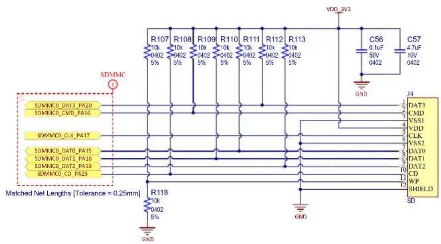
text_image
VDD_3V3 R107 R108 R109 R110 R111 R112 R113 10k 10k 10k 10k 10k 10k 10k 10k 10k 10k 10k 10k 10k 10k 10k 10k 10k 10k 10k 10k 10k 10k 10k 10k 10k 10k 5% 0402 0402 0402 0402 0402 0402 0402 0402 0402 0402 SDMMC GND C56 C57 0.1uF 50V 10V 0402 4.7uF 10V 0402 J4 DAT3 CMD VSS1 VDD CLK VSS2 DAT10 DAT1 DAT2 CD WP SHIELD SD SDMMC0_DAT3_PA2D SDMMC0_CMD_PA16 SDMMC0_CLK_PA17 SDMMC0_DAT0_PA15 SDMMC0_DAT1_PA18 SDMMC0_DAT2_PA19 SDMMC0_CI_PA23 Matched Net Lengths [Tolerance = 0.25mm] R118 10k 0402 5% GND3.4.9 mikroBUS Interface
The SAM9X60-EK hosts a pair of 8-pin female headers (J14) implementing a mikroBUS socket. For details, refer to the mikroBUS documentation on https://www.mikroe.com/mikrobus.
Figure 3-39. mikroBUS Interface

text_image
J14 MBUS_AD1_PB15 1 AN PWM 16 MBUS_PWM_PB13 MBUS_RST_PB14 2 RST INT 15 MBUS_INT_PB18 MBUS_NFC50_PA14 3 CS RX 14 MBUS_RX MBUS_SPCK_PA13 4 SCK TX 13 MBUS_TX MBUS_MISO_PA11 5 MISO SCT 12 MBUS_TWCK MBUS_MOSI_PA12 6 MOSI SDA 11 MBUS_TWD 7 +3.3V +5V 10 MBUS_TWD 8 GND GND 9 T mikroBUS HCST GNDGNDTable 3-20. mikroBUS Connector J14 Pin Assignment
| Function PIO Mbus Signal Pin # Pin # Mbus Signal PIO Function | |||||||
| Analog input PB15 AN 1 16 PWM PB13 PWM | |||||||
| Reset PB14 RST 2 15 INT PB18 Interrupt | |||||||
| SPI Chip Select | PA14 | SPI_NPCS | 3 14 UART_RX | PA21 UART receive (output from Mbus into SAM) | |||
| SPI clock | PA13 | SPI_SPCK | 4 | 13 | UART_TX | PA22 | UART transmit (input from SAM into Mbus) |
| SPI MISO | PA11 | SPI_MISO | 5 | 12 | TWI_SCL | PA31 | TWI clock |
| SPI MOSI | PA12 | SPI_MOSI | 6 | 11 | TWI_SDA | PA30 | TWI data |
| VCC_ | 3V3 Supply | 7 10 5V | Supply _ | VDD | |||
| GROUND | _ | GND | 8 | 9 | GND | _ | Ground |
Note: Enabling the ATWILC3000 interface prevents the UART functionality from being used with the mikroBUS connector. See 3.4.3 Wi-Fi/Bluetooth Module (Optional).
3.4.10 GPIO Interface
The SAM9X60-EK board features a 40-pin connector (Raspberry Pi ^® compatible) for free use.
Figure 3-40. GPIO Connector

text_image
VDD_3V3VDD_MAIN_5V J16 EXT40_TWD EXT40_TWCK EXT40_I25MCK_PB23 EXT40_GPIO_PA02 EXT40_GPIO_PA04 EXT40_GPIO_PA03 EXT40_SPI_MOSI_PA12 EXT40_SPI_MISO_PA11 EXT40_SPI_SCLK_PA13 EXT40_CLK1_PC31 EXT40_CLK2_PB13 EXT40_PWM1_PB12 EXT40_I25WS_PB20 EXT40_GP7 EXT40_TXD EXT40_RXD EXT40_I25CK_PB19 EXT40_GPS EXT40_GP6 EXT40_GPIO_PA14 EXT40_NPCS1_PA07 EXT40_NPCS2_PA08 EXT40_PWM0_PB11 EXT40_GPIO_PB24 EXT40_I2SDIN_PB21 EXT40_I2SDOUT_PB22 HDR-2.54 Male 2x20 TSW-120-D7-G-DTable 3-21. GPIO Connector J16 Pin Assignment
| Signal Pin No Pin No Signal | |||
| +3V3 1 2 +5V | |||
| EXT40_TWD 3 4 +5V | |||
| EXT40_TWCK 5 6 Ground | |||
| EXT40_I2SMCK_PB23 7 8 EXT40_TXD | |||
| GND 9 10 EXT40_RXD | |||
| EXT40_GPIO_PA02 11 12 EXT40_I2SCK_PB19 | |||
| EXT40_GPIO_PA03 13 14 Ground | |||
| EXT40_GPIO_PA04 15 16 EXT40_GP5 | |||
| +3V3 17 18 EXT40_GP6 | |||
| EXT40_SPI_MOSI_PA12 | 19 20 Ground | ||
| EXT40_SPI_MISO_PA11 21 22 EXT40_GPIO_PA14 | |||
| EXT40_SPI_SCLK_PA13 | 23 24 EXT40_NPCS1_PA07 | ||
| GND 25 26 EXT40_NPCS2_PA08 | |||
| NC | 27 28 NC | ||
| EXT40_CLK1_PC31 | 29 30 Ground | ||
| EXT40_CLK2_PB13 | 31 32 EXT40_PWM0_PB11 | ||
| EXT40_PWM1_PB12 | 33 34 Ground | ||
| EXT40_I2SWS_PB20 | 35 36 EXT40_GPIO_PB24 | ||
| EXT40_GP7 | 37 38 EXT40_I2SDIN_PB21 | ||
| GND 39 40 EXT40_I2SDOUT_PB22 |
3.5 User Interaction and Debugging
The SAM9X60-EK includes two main debugging interfaces to provide debug-level access to the SAM9X60-EK:
• One UART through the USB/J-Link-OB CDC feature
- Two JTAG interfaces, one connected directly to the MPU using connector J23 and one through the J-Link-OB interface USB port J21
3.5.1 Serial Debug Com Port (FTDI)
The SAM9X60-EK board features a dedicated serial port for debugging, accessible through header J24. Various interfaces can be used as a USB/Serial DBGU port bridge, such as the FTDI TTL-232R USB-to-TTL serial cable.
Figure 3-41. Serial Debug Com Port
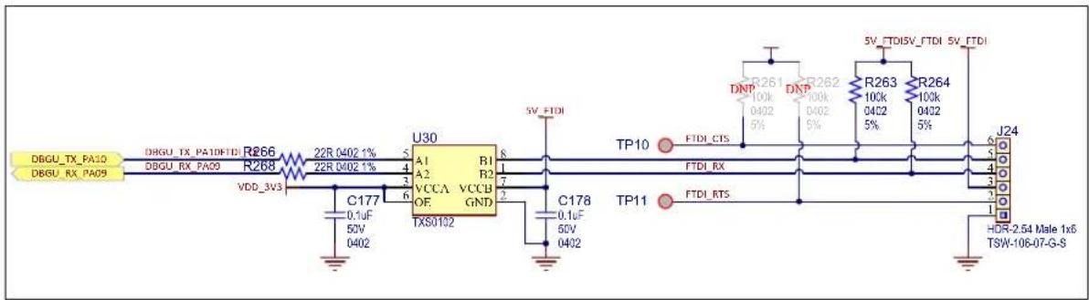
text_image
DBGU_TX_PA10 DBGU_RX_PA09 DRGU_TX_PAIDFTDI R266 22R 0402 1% R268 22R 0402 1% VDD_3VS C177 0.1uF 50V 0402 U30 A1 R1 A2 R2 VCCA VCCB OF GND TXS0102 5V_FTDI C178 0.1uF 50V 0402 TP10 FTDI_CTS FTDI_RX TP11 FTDI_RTS 5V_FTDISV_FTDI 5V_FTDI R261 100k DNP R262 100k DNP 100k 100k DNP 100k 100k DNP 100k 100k DNP 100k 100k DNP 100k 100k DNP 100k 100k DNP 100k 100k DNP 100k 100k DNP 100k 10M-2.54 Male 1x6 TSW-106-07-G-STable 3-22. Debug Com Port Signal Descriptions
| PIO Signal Name Shared Signal Description | ||
| PA09 DBGU_RX_PA09 DEBUG Receive data | ||
| PA10 DBGU_TX_PA10 DEBUG Transmit data |
3.5.2 Debug JTAG
A 20-pin JTAG header (J23) is provided on the SAM9X60-EK board to facilitate software development and debugging using various JTAG emulators. The interface signals have a voltage level of 3.3V.
Figure 3-42. JTAG Connector

text_image
VDD_3V3 R260 100k 0402 5% DNP R259 100k 0402 5% DNP R258 100k 0402 5% R257 100k 0402 5% R256 100k 0402 5% VDD_3V3 J23 1 2 3 4 5 6 7 8 9 10 11 12 13 14 15 16 17 18 19 20 JTAG_CONN_TDI JTAG_CONN_TMS JTAG_CONN_TCK JTAG_CONN_RTCX JTAG_CONN_TDO JTAG_CONN_NRST R265 100R 0402 1% HDR-2.54 Male 2x10- 302-R201_GNDTable 3-23. JTAG/ICE Connector J23 Pin Assignment
| Signal Pin No Pin No Signal | |||
| +3.3V 2 1 +3V3 | |||
| GND 4 3 NC | |||
| GND 5 5 TDI | |||
| GND 8 7 TMS | |||
| GND 10 9 TCK | |||
| GND 12 11 RTCK | |||
| GND 14 13 TDO | |||
| GND 16 15 nRST | |||
| GND 18 17 NC | |||
| GND 20 19 NC |
3.5.3 Embedded Debugger (J-Link-OB) Interface
The SAM9X60-EK includes a built-in SEGGER J-Link-On-Board (J-Link-OB) device. The functionality is implemented with an ATSAM3U4C microcontroller in an LFBGA100 package. The ATSAM3U4C provides the functions of the JTAG interface and a bridge from USB to Serial debug port (known as CDC, or communication class device). The bi-colored LED (D9) shows the status of the J-Link-On-Board device.
The J-Link-OB device is designed to provide an efficient, low-cost, on-board alternative to the standard J-Link or SAM-ICE.
Its own dedicated USB port acts as a power source for this block (which is separated from the rest of the system) and provides the communication link to program and debug the MPU.
Figure 3-43. J-Link-OB with J-Link-CDC Interface
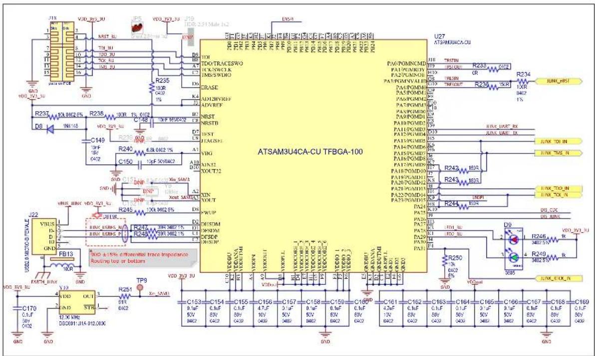
text_image
J18 R01 1 2 3 4 5 6 7 8 9 10 11 12 13 14 15 16 VDD_30V_3U VDD_30V_3U VDD_30V_3U VDD_30V_3U VDD_30V_3U VDD_30V_3U VDD_30V_3U VDD_30V_3U VDD_30V_3U VDD_30V_3U VDD_30V_3CU GND VDOS_VDD_PCEB GND D8 R237 D6 R236 IN1-128 R235 10F 0.002 6.55 R236 10X 0.002 R235 10X 0.002 R235 10X 0.002 R235 10X 0.002 R235 10X 0.002 R235 10X 0.002 R235 10X 0.002 R235 10X 0.001 R235 10X 0.001 R235 10X 0.001 R235 10X 0.001 R235 10X 0.001 R235 10X 0.001 R235 10X 0.001 R235 10X VDOS_VDD_PCEB VDOS_VDD_PCEB VDOS_VDD_PCEB VDOS_VDD_PCEB VDOS_VDD_PCEB VDOS_VDD_PCEB VDOS_VDD_PCEB VDOS_VDD_PCEB VDOS_VDD_PCEB VDOS_VDD_PCEB VDOS_VDD_PCEB VDOS_VDD_PCEB VDOS_VDD_PCEB VDOS-VDD_PCEB VDOS-VDD_PCEB VDOS-VDD_PCEB VDOS-VDD_PCEB VDOS-VDD_PCEB VDOS-VDD_PCEB VDOS-VDD_PCEB VDOS-VDD_PCEB VDOS-VDD_PCEB VDOS-VDD_PCEB VDOS-VDD_PCEB VDOS-VDD_PCEB VDOS-VDD_PCEBE VDOS-VDD_PCEB VDOS-VDD_PCEB VDOS-VDD_PCEB VDOS-VDD_PCEB VDOS-VDD_PCEB VDOS-VDD_PCEB VDOS-VDD_PCEB VDOS-VDD_PCEB VDOS-VDD_PCEB VDOS-VDD_PCEB VDOS-VDD_PCEB VDOS-VDD_PCEB VDOS-TRACESWO ICK-SWCLK IMS/SWDO CRASE ADI2HYREF ADVREF NRST NRSTB TRST TTAGSHE VBG XIN32 XOUT12 XIN ROUT SWUP DUSDM DPSDM DPSDP DUSDM DUSDM DUSDM DUSDM DUSDM DUSDM DUSDM DUSDM DUSDM DUSDM DUSDM DUSDM DUSDM DUSDM DUSDM DUSDM DUSDM DUSDM DUSDM DUSDM DUSDM DUSDM DUSDM DUSDM DUSDM DUSDM DUSDM DUSDM DUSDM DUSDM DUSDM DUSDM DUSDM DUSDMTable 3-24. J-Link-OB and J-Link-CDC LED D9 Status
| LED D9 State Description | |
| Red and Green Off J-Link (SAM3U device) is not programmed, or J20 and J21 are installed. | |
| Red On J-Link (SAM3U device) is programmed but J-Link is disabled (J20 installed). | |
| Green Flashing J-Link is operational but the USB port is not connected. | |
| Green On J-Link-OB is connected and ready. | |
The ATSAM3U microcontroller is powered only through the J-Link USB connector. This way, the programmer IC is separated from the rest of the system and the user can have a better reading of the power that the system is drawing when interrogating the power measurement devices placed on the board.
The MIC5528 has been selected to convert the 5V coming from the USB connector into the 3.3V rail needed by the microcontroller. The MIC5528 is a simple low-power, low dropout regulator designed for optimal performance in a very small footprint. It is capable of sourcing up to 500 mA of output current while only drawing 38 A of operating current. For more information about the MIC5528, refer to the product web page.
Figure 3-44. J-Link-OB Power Supply
text_image
VBUS_ILINK VBUS_JLINKVDD_3V3_3U U28 6 VTN 1 VOUT 2 FN 4 NC 5 GND 3 FP 7 MIC5528 3V3 603 C171 2.2uF 16V 5 VDD_3V3_3U C172 2.2uF 16V 50V 0603 C173 0.1uF 0402If the user does not require the on-board programming feature, this section can be left unpowered, with no impact on the rest of the system. A level shifter has been placed on the DEBUG UART line between the SAM9X60 MPU and the on-board programmer to properly separate the two voltage domains.
Figure 3-45. J-Link-OB Level Shifter

text_image
DIS_CDC R252 22R0401% R254 22R0401% VDD_3V3 U29 A1 B1 A2 B2 VCCA VCCB OE GND TXS0102 C174 0.1uF 50V 0402 C175 0.1uF 50V 0402 GND6ND JLINK_UART_TX JLINK_UART_RX DBGU_RX_PA09 DBGU_TX_PA10Jumper JP6/J20 disables the J-Link-OB JTAG functionality. When installed (J20 shorted), a quad analog switch (U31/U32) routes the JTAG interface of the SAM9X60 to the 20-pin header J23.
- Jumper JP6/J20 not installed: J-Link-OB-ATSAM3U4C is enabled and fully functional.
- Jumper JP6/J20 installed: J-Link-OB-ATSAM3U4C is disabled and an external JTAG controller can be used through the 20-pin JTAG port J23.
Figure 3-46. Disable J-Link CDC

text_image
JP7 Shunt 2.54mm 1x2 DIS_CDC VDD_3V3_3U R241 10k 0402 5% J21 2:1 HDR-2.54Max2 GNDFigure 3-47. JTAG Switch

text_image
DIS JUNK U31 S VCC 16 E GND 8 C176 0.1μF 50V C402 JTAG_TCK 4 JTAG_TDI 7 JTAG_TDO 9 JTAG_TMS 12 YA 10A 2 T1A 3 YB 10B 5 11B 6 YC 10C 11 11C 10 YD 10D 14 11D 13 IDTC3VH257PAG JTAG_CONN TCK JUNK_TCK_IN JTAG_CONN TDI JUNK_TDI_IN JTAG_CONN_TDO JUNK_TDO_IN JTAG_CONN_TMS JUNK_TMS_IN
text_image
R270 100k04025½ VDD_3V3 U32 DIS_JUNK C179 0.1uF 50V C402 Q16 BSS138N JTAG_RTCK JTAG_RST DTQS3VH125 1Y 1A 3 2Y 2A 6 3Y 3A 11 4Y 4A 14 JTAG_CONN_RTCK JLINK_RTCK_IN JTAG_CONN_nRST JLINK_nRSTIn addition to the J-Link-OB functionality, the ATSAM3U4C microcontroller provides a bridge to a debug serial port (DBGU) of the main board processor. The port is made accessible over the same USB connection used by JTAG by implementing a Communication Device Class (CDC), which allows a terminal communication with the target device.
This feature is enabled/disabled by jumper J21.
- Jumper J21 not installed: the J-Link-OB CDC function is enabled and fully functional.
- Jumper J21 installed: the J-Link-OB CDC function is disabled.
The USB CDC converts the USB device into a serial communication device. The target device running the CDC is recognized by the host as a serial interface (USB2COM, virtual COM port) without the need of installing a special host driver (the CDC is standard). All PC software using a COM port work without modifications with this virtual COM port. Under Microsoft ^® Windows ^® , the device shows up as a COM port; under Linux ^® , as a /dev/ACMx device. This enables the user to use host software which was not designed to be used with USB, such as a terminal program.
Figure 3-48. Disable J-Link JTAG

text_image
JP6 Shunt 2.54mm 1x2 DIS_JLINK VDD_3V3_3U R232 10k 0402 5% J20 1 HDR-2.54 Male 1x23.5.4 Push Button Switches
The SAM9X60-EK features four push buttons:
- One User push button (SW1) connected to PIO_PD18. This is left at user usage.
- One Wake-up push button (SW2) connected to the SAM9X60 WKUP pin; when pressed, the processor recovers from shutdown.
- One Board Reset push button (SW3); when pressed, the processor is reset.
- One Disable Boot push button (SW4); if kept pressed during power-up, the processor is prevented from booting off the on-board memories (QSPI and NAND Flash), thereby enabling booting from other sources or into ROM Code.
Figure 3-49. User Push Buttons

text_image
VDD_3V3 R186 10k 0402 5% USER_BUTTON_PD18 R192 100R0402 1% SW1 1 2 3 TL3301NF260QG GNDGND VDDBU R194 100k 0402 5% WAKE_UP R197 100R0402 1% SW2 1 2 3 TL3301NF260QG GNDGND USER_nRST C145 0.1uF 0402 1 2 3 TL3301NF260QG GND SW3 1 2 3 DIS_BOOT DIS_BOOT SW4 1 2 3 TL3301NF260QG GND3.5.5 Disable Boot
On-board push button SW4 and/or jumper J13 control the selection (CS#) of the bootable memory components (QSPI and NAND FLASH) using a non-inverting 3-state buffer.
The rule of operation is:
- SW4 (DISABLE_BOOT) or J13 shorted = booting from QSPI and NAND FLASH is disabled.
- LED D6 indicates the state of the DIS_BOOT signal.
- Red = on-board boot memories are disabled.
- Green = on-board boot memories are enabled.
Figure 3-50. Disable Boot
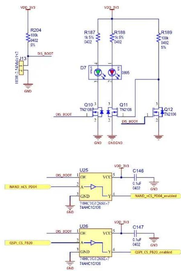
Note: The "Disable Boot" mechanism does not disable booting from the SD card connector. The user must remove the SD card in order to disable booting from it.
3.5.6 RGB LED
The SAM9X60-EK board features one RGB LED. The three LED cathodes are controlled via GPIO PWM pins.
Figure 3-51. User LEDs

text_image
LED_BLUE_PB13 R195 100R 0402 1% GND R196 10k 0402 5% R199 1k0-02 Q13 TN2106 5% I 2 GND R200 100R 0402 1% GND R202 10k 0402 5% I 3 Q14 TN2106 5% I 2 GND R201 1k0-02 Q15 TN2106 5% I 3 R203 2.2k0-02 Q15 TN2106 5% I 2 GND VDD 3V3 LD1 CLV1A-FKB-CK1NIG1B57R4S3 LED_GREEN_PB12 LED_RDP_PB11 R206 100R 0402 1% GND R207 DNP1A 0402 5% I 3 Q15 TN2106Table 3-25. RGB LED PIOs
| Signal PIO Function | ||
| LED_RED_PB11 PB11 PWMH1 | ||
| LED_GREEN_PB12 PB12 PWML1 | ||
| LED_BLUE_PB13 PB13 PWML0 |
4. Installation and Operation
4.1 System and Configuration Requirements
The SAM9X60-EK requires the following:
- Personal Computer
- USB cable (provided in the kit box)
4.2 Board Setup
Follow these steps before using the SAM9X60-EK:
- Unpack the board, taking care to avoid electrostatic discharge.
- Check the default jumper settings (see 2.5 Default Jumper Settings).
- Connect the Micro-USB cable to connector J7 (USB-A port).
- Connect the other end of the cable to a free port on your PC.
- Open a terminal (console 115200, N, 8, 1) on your PC.
- Reset the board. A startup message appears on the console.
5. Errata
5.1 Inoperative LED
On SAM9X60-EK Rev. B, the Ethernet activity LED on RJ45 connector J5 is inoperative due to an incorrect LED connection. This issue is solved in Rev. 2, as shown in the following picture. Nevertheless, the Ethernet port is perfectly operational on Rev. B boards.
Figure 5-1. RJ45 Connector Right LED Connection Change from Rev. B to Rev. 2
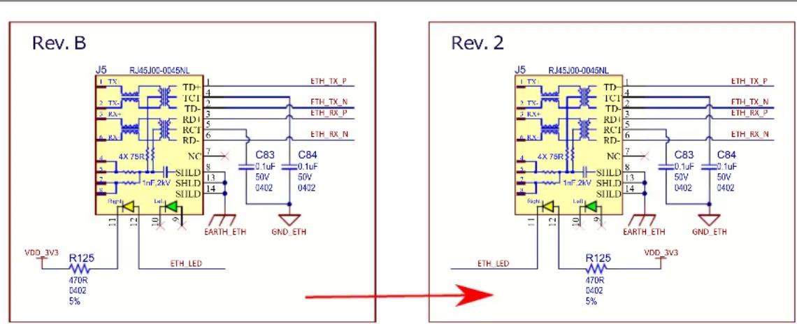
text_image
Rev. B J5 RJ45J00-0045NL 1 TX 2 RX 3 RX 4 RX 5 RX 6 RX 7 RX 8 RX 9 RX 10 RX 11 RX 12 RX 13 RX 14 RX 15 RX 16 RX 17 RX 18 RX 19 RX 20 RX 21 RX 22 RX 23 RX 24 RX 25 RX 26 RX 27 RX 28 RX 29 RX 30 RX 31 RX 32 RX 33 RX 34 RX 35 RX 36 RX 37 RX 38 RX 39 RX 40 RX 41 RX 42 RX 43 RX 44 RX 45 RX 46 RX 47 RX 48 RX 49 RX 50 RX 51 RX 52 RX 53 RX 54 RX 55 RX 56 RX 57 RX 58 RX 59 RX 60 RX 61 RX 62 RX 63 RX 64 RX 65 RX 66 RX 67 RX 68 RX 69 RX 70 RX 71 RX 72 RX 73 RX 74 RX 75 RX 76 RX 77 RX 78 RX 79 RX 80 RX 81 RX 82 RX 83 RX 84 RX 85 RX 86 RX 87 RX 88 RX 89 RX 90 RX 91 RX 92 RX 93 RX 94 RX 95 RX 96 RX 97 RX 98 RX 99 RX 100 RX 101 RX 102 RX 103 RX 104 RX 105 RX 106 RX 107 RX 108 RX 109 RX 110 RX 111 RX 112 RX 113 RX 114 RX 115 RX 116 RX 117 RX 118 RX 119 RX 120 RX 121 RX 122 RX 123 RX 124 RX 125 RX5.2 Booting Issue
On SAM9X60-EK Rev. B, Rev. 2 and Rev. 3 boards, when booting from NAND Flash memory MT29F4G08ABAEA, the boot sequence does not execute the first time the board powers up; booting occurs only after the user presses the Reset button.
The reason is that the MT29F4G08ABAEA memory does not follow the ONFI specification, which requires a maximum 5 s internal reset time after the RESET command (0xFF) has been sent. It is therefore not ready when the SAM9X60 needs to read boot code from it.
We recommend not to use MT29F4G08ABAEA in your design.
5.3 Powering-Up Issue
There is a known issue that can occur on the SAM9X60-EK Rev. B, Rev. 2 and Rev. 3 boards if the user tries to mount and use the optional WILC3000 module together with the LCD or with the Ethernet PHY.
With WILC3000, a special power-up sequence applies, requiring that the reset line be held low for a specific period of time. However, as all devices share the same reset line, this can cause communication disruptions during runtime.
To solve this issue, we recommend separating the reset line going to the WILC3000 by cutting the trace and connecting it to a free GPIO from the 40-pin GPIO connector (J16). Our recommendation is to use PC31 (pin 29), as this is the one implemented in our current Linux distribution.
The following figures provide board modification guidance.
Figure 5-2. Board Modification Step 1
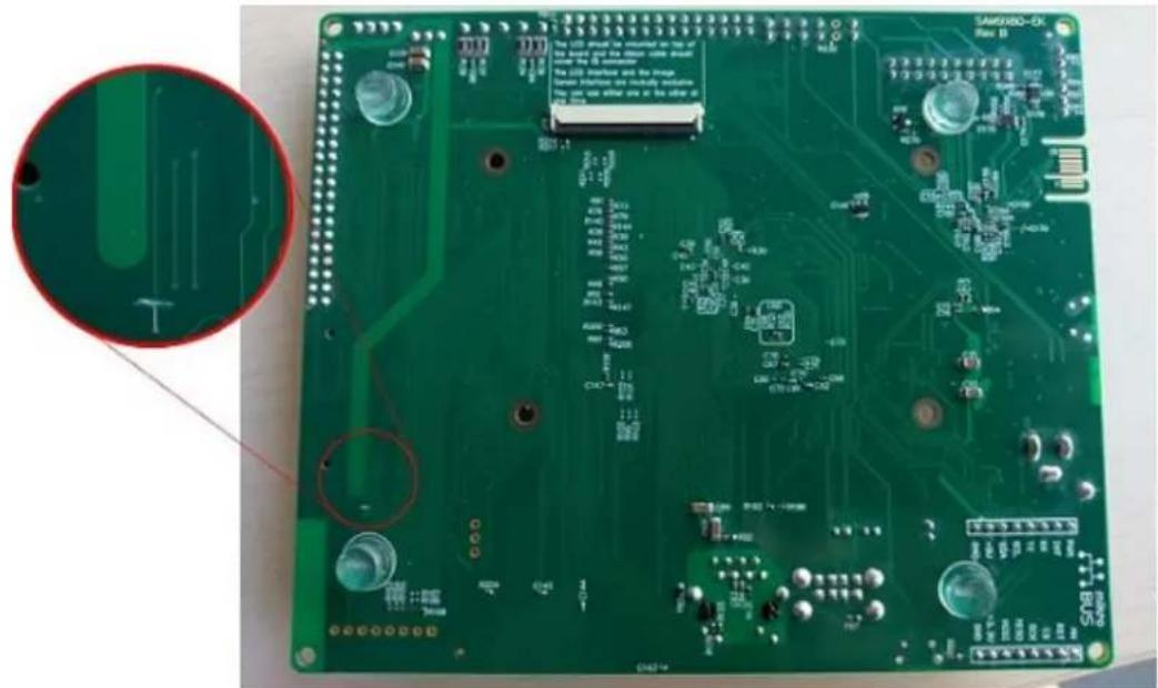
natural_image
Close-up of a green printed circuit board (PCB) with visible traces, pads, and components, no readable text or symbols.Figure 5-3. Board Modification Step 2

text_image
SAMX80-EX Rev 13 The LCD should be mounted on a 46% of the brand and the motion cable should have the 2D connection The LCD Interface and the Image Sensor Interface are exclusively evaluated. This can use either one or the other of the device. C275 C276 C277 C278 C279 C280 C281 C282 C283 C284 C285 C286 C287 C288 C289 C290 C291 C292 C293 C294 C295 C296 C297 C298 C299 C300 C301 C302 C303 C304 C305 C306 C307 C308 C309 C310 C311 C312 C313 C314 C315 C316 C317 C318 C319 C320 C321 C322 C323 C324 C325 C326 C327 C328 C329 C330 C331 C332 C333 C334 C335 C336 C337 C338 C339 C340 C341 C342 C343 C344 C345 C346 C347 C348 C349 C350 C351 C352 C353 C354 C355 C356 C357 C358 C359 C360 C361 C362 C363 C364 C365 C366 C367 C368 C369 C370 C371 C372 C373 D100000000000000000000000000000000000000000000000000000000000000000000000000000000000000000000000000005.4 Resistor Mislabeling
There is a known silkscreen error on the SAM9X60-EK Rev. B and Rev. 2 boards: resistor R65 is mistakenly labeled as R72 whereas resistor R72 has no designator. See the following figure.
Figure 5-4. R65 and R72 Resistor Identification
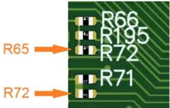
text_image
R65 R72 R66 R195 R72 R716. Appendix. Schematics and Layouts
This appendix contains the following schematics and layouts for the SAM9X60-EK board:
- Block Diagram
• Power Supply - SAM9X60 Processor
- Processor I/Os
- Processor I/O Expansions
- On-board Memories
- USB Interfaces
- Ethernet MAC
- Wi-Fi/Bluetooth
• SDMMC, CAN and CLASSD - Expansion Connectors
- User Interaction
- On-board J-Link
Figure 6-1. Block Diagram
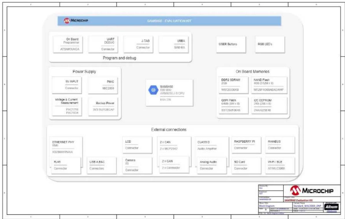
flowchart
graph TD
    A["Microchip"] --> B["Program and debug"]
    B --> C["Power Supply"]
    C --> D["External connections"]
    D --> E["External connections"]

    subgraph Program and debug
        F["On Board Programmer AT5AM3UAICA"] --> G["UART DEBUG Connector"]
        H["J-TAB Connector"] --> I["USBA SAM-RA"]
        J["USER Buttons"] --> K["RGB LED's"]
    end

    subgraph External connections
        L["SV INPUT Connector"] --> M["PMIC MIC2099"]
        N["Voltage & Current Measurement PAC1718 PAC1934"] --> O["Backup Power 3VO SUPERCAP"]
        P["SAM9X60 640 MHz APM9X5C J-S CPU BSA 22A"] --> Q["On Board Memories"]
        R["DDR2 SDRAM 200 WST2006KB"] --> S["NAND Flash 400 (312M x 8) MT29F400SABEAWP"]
        T["QSPI Flash 6480 (ON x 8) SST20V70645"] --> U["L2C EEPROM 290 (256 x 8) Z4AA625E48"]
    end

    subgraph External connections
        V["ETHERNET PHY SIM X5ZB603INNAIA"] --> W["LCD Connector"]
        X["RJ40 Connector"] --> Y["USB A,B&C Connectors"]
        Z["Camera ISI Connector"] --> AA["2 x CAN 2 x MCP2542"]
        AB["CLA33 D Audio Amplifier"] --> AC["ANalog Audio Connector"]
        AD["RASPBERRY FI Connector"] --> AE["SD Card Connector"]
        AF["microBUS Connector"] --> AG["WIFI / BLE ATWILC3000"]
    end

    subgraph External connections
        AH["External Connection"] --> AI["External Connection"]
    end

    style A fill:#f9f,stroke:#333
    style B fill:#ccf,stroke:#333
    style C fill:#cfc,stroke:#333
    style D fill:#fcc,stroke:#333
    style E fill:#ffc,stroke:#333
    style F fill:#fcc,stroke:#333
    style G fill:#fcc,stroke:#333
    style H fill:#fcc,stroke:#333
    style I fill:#fcc,stroke:#333
    style J fill:#fcc,stroke:#333
    style K fill:#fcc,stroke:#333
    style L fill:#fcc,stroke:#333
    style M fill:#fcc,stroke:#333
    style N fill:#fcc,stroke:#333
    style O fill:#fcc,stroke:#333
    style P fill:#fcc,stroke:#333
    style Q fill:#fcc,stroke:#333
    style R fill:#fcc,stroke:#333
    style S fill:#fcc,stroke:#333
    style T fill:#fcc,stroke:#333
    style U fill:#fcc,stroke:#333
    style V fill:#fcc,stroke:#333
    style W fill:#fcc,stroke:#333
    style X fill:#fcc,stroke:#333
    style Y fill:#fcc,stroke:#333
    style Z fill:#fcc,stroke:#333
    style AA fill:#fcc,stroke:#333
    style AB fill:#fcc,stroke:#333
    style AC fill:#fcc,stroke:#333
    style AD fill:#fcc,stroke:#333
    style AE fill:#fcc,stroke:#333
    style AF fill:#fcc,stroke:#333
Figure 6-2. Power Supply
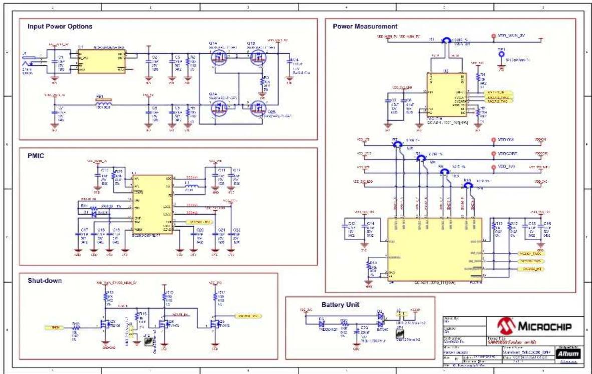
text_image
Input Power Options Power Measurement PMIC Shut-down Battery Unit MICROCHIP Microchip Faser Film SAPRMSO Emitter unit Power Supply Standard MicroChip DIP AlbumFigure 6-3. SAM9X60 Processor

text_image
SAM9X60 Power SAM9X60 POWER SUPPLY SAM9X60 DDR Controller SAM9X60 Clocks SAM9X60 Core DDR_VREF SAM9X60 Reset MicroCHIP SAMS2500 Emitter on Kit SAMS2500 Emitter on Kit Microchip SAV9600 Standard MLC800 DHP Altum 1 2 3 4 5 6 Dissuizing case should be placed as close as possible in their corresponding power bank Place C15 close to L11 or P13, and place C80 close to P10Figure 6-4. Processor I/Os
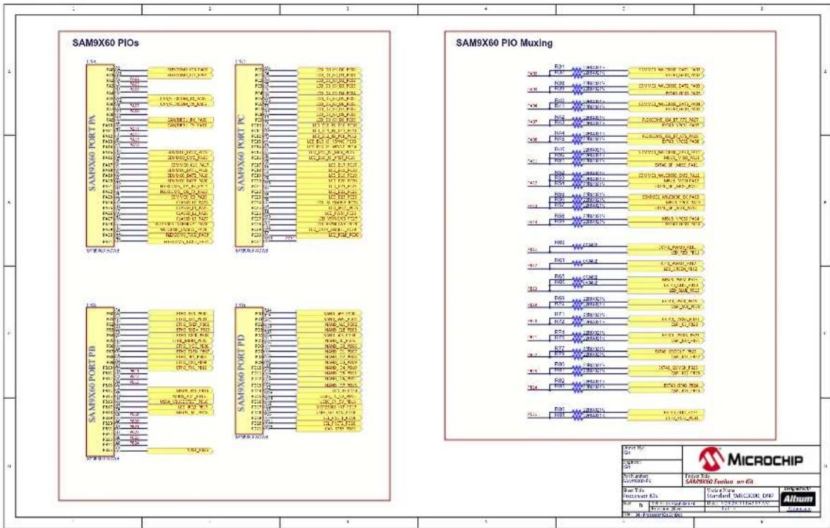
other
SAM9X60 PIOs - Panel 1: SAM9X60 PORT PA - Panel 2: SAM9X60 PORT KC - Panel 3: SAM9X60 PORT PB - Panel 4: SAM9X60 PORT PD Microchip - Microchip Pin - Microchip Label - Microchip Type - Microchip ID - Microchip ID/Label - Microchip ID/Label - Microchip ID/Label - Microchip ID/Label - Microchip ID/Label - Microchip ID/Label - Microchip ID/Label - Microchip ID/Label - Microchip ID/Label - Microchip ID/Label - Microchip ID/Label - Microchip ID/Label - Microchip ID/Label - Microchip ID/Label - Microchip ID/Label (1) (2) (3) (4) (5) (6) (7) (8) (9) (10) (11) (12) (13) (14) (15) (16) (17) (18) (19) (20) (21) (22) (23) (24) (25) (26) (27) (28) (29) (30) (31) (32) (33) (34) (35) (36) (37) (38) (39) (40) (41) (42) (43) (44) (45) (46) (47) (48) (49) (50) (51) (52) (53) (54) (55) (56) (57) (58) (59) (60) (61) (62) (63) (64) (65) (66) (67) (68) (69) (70) (71) (72) (73) (74) (75) (76) (77) (78) (79) (80) (81) (82) (83) (84) (85) (86) (87) (88) (89) (90) (91) (92) (93) (94) (95) (96) (97) (98) (99) (100) Microchip - Microchip Pin - Microchip Label - Microchip ID - Microchip ID/Label - Microchip ID/Label - Microchip ID/Label - Microchip ID/Label - Microchip ID/Label - Microchip ID/Label - Microchip ID/Label - Microchip ID/Label - Microchip ID/Label - Microchip ID/Label - Microchip ID/Label - Microchip ID/Label - Microchip ID/Label - MicroChip MicroChip - MicroChip Pin - MicroChip Label - MicroChip ID - MicroChip ID/Label - MicroChip ID/Label - MicroChip ID/Label - MicroChip ID/Label - MicroChip ID/Label - MicroChip ID/Label - MicroChip ID/Label - MicroChip ID/Label - MicroChip ID/Label - MicroChip ID/Label - MicroChip ID/Label - MicroChip ID/Label - MicroChip ID/Label - MicroChip ID/Label - MicroChip ID/Label SAMS port pin configuration table for each port's mode and pin number. SAMS port pin configuration table for each port's mode and pin number. SAMS port pin configuration table for each port's mode and pin number. SAMS port pin configuration table for each port's mode and pin number. SAMS port pin configuration table for each port's mode and pin number. SAMS port pin configuration table for each port's mode and pin number. SAMS port pin configuration table for each port's mode and pin number. SAMS port pin configuration table for each port’s mode and pin number. SAMS port pin configuration table for each port's mode and pin number. SAMS port pin configuration table for each port's mode and pin number. SAMS port pin configuration table for each port's mode and pin number. SAMS port pin configuration table for each port's mode and pin number. SAMS port pin configuration table for each port's mode and pin number. SAMS port pin configuration table for each port's mode and pin number. SAMS port pin configurations are shown in the schematic.Figure 6-5. Processor I/O Expansions

text_image
CAN1 / EXT40 UART Selection Port Expander CAN0 / DEBUG UART Selection Upper Right Board TWI MikroBUS UART / WILC BT UART Selection Lower Left Board TWI MICROCHIP Microchip CAMERAO Evaluator on Kit Procoquer 10 Expansions Standard WILC3000 2MP Altum No. No. 100000000000000000000000000000000000000000000000000000000000000000000000000000000000000000000000Figure 6-6. On-board Memories

text_image
TWI EEPROM 2Gb DDR2-800 SDRAM 16bit Serial Quad I/O Flash 4Gb NAND Flash TSOP-48 MicroCHIP Micro Chip Micro Chip Micro Chip Micro Chip Micro Chip Micro Chip Micro Chip Micro Chip Micro Chip Micro Chip Micro Chip Micro Chip Micro Chip Micro Chip Micro Chip Micro Chip Micro Chip Micro Chip Micro Chip Micro Chip Micro Chip Micro Chip Micro Chip Micro Chip Micro Chip Micro Chip Micro Chip Micro Chip Micro Chip Micro Chip Micro Chip Micro Chip Micro Chip Micro ChipFigure 6-7. USB Interfaces
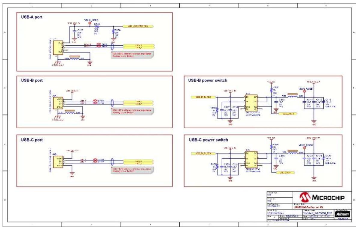
text_image
USB-A port USB-B port USB-B power switch USB-C power switch MicroCHIP SAMS/2000-CT USB Interface USB-1.5V 0.1V 0.1V 0.1V 0.1V 0.1V 0.1V 0.1V 0.1V 0.1V 0.1V 0.1V 0.1V 0.1V 0.1V 0.1V 0.1V 0.1V 0.1V 0.1V 0.1V 0.3V USB-1.5V 0.1V 0.1V 0.1V 0.1V 0.1V 0.1V 0.1V 0.1V 0.1V 0.1V 0.1V 0.1V 0.1V 0.1V 0.1V 0.1V 0.1V 0.1V 0. USB-2.5V 0.2V 0.2V 0.2V 0.2V 0.2V 0.2V 0.2V 0.2V 0.2V 0.2V 0.2V 0.2V 0.2V 0.2V 0.2V 0.2V USB-3.5V 0.3V 0.3V 0.3V 0.3V 0.3V 0.3V 0.3V 0.3V 0.3V 0.3V 0.3V 0.3V 0.3V 0.3V USB-4.5V 0.4V 0.4V 0.4V 0.4V 0.4V 0.4V 0.4V 0.4V 0.4V 0.4V 0.4V USB-5.5V 0.5V 0.5V 0.5V 0.5V 0.5V 0.5V 0.5V 0.5V 0.5V USB-6.5V 0.6V 0.6V 0.6V 0.6V 0.6V USB-7.5V 0.7V 0.7V USB-8.5V 0.8V USB-9.5V USB-10A USB-11A USB-12A USB-13A USB-14A USB-15A USB-16A USB-17A USB-18A USB-19A USB-20A USB-21A USB-22A USB-23A USB-24A USB-25A USB-26A USB-27A USB-28A USB-29A USB-30A USB-31A USB-32A USB-33A USB-34A USB-35A USB-36A USB-37A USB-38A USB-39A USB-40A USB-41A USB-42A USB-43A USB-44A USB-45A USB-46A USB-47A USB-48A USB-49A USB-50A USB-51A USB-52A USB-53A USB-54A USB-55A USB-56A USB-57A USB-58A USB-59A USB-60A USB-61A USB-62A USB-63A USB-64A USB-65A USB-66A USB-67A USB-68A USB-69A USB-70A USB-71A USB-72A USB-73A USB-74A USB-75A USB-76A USB-77A USB-78A USB-79A USB-80A USB-81A USB-82A USB-83A USB-84A USB-85A USB-86A USB-87A USB-88A USB-89A USB-90A USB-91A USB-92A USB-93A USB-94A USB-95A USB-96A USB-97A USB-98A USB-99A USB-COS/CCS/CCS/CCS/CCS/CCS/CCS/CCS/CCS/CCS/CCS/CCS/CCS/CCS/CCS/CCS/CCS/CCS/CCS/CCS/CCS/CCS/CCS/CCS/CCS/CCS/CCS/CCS/CCS/CCS/CCS/CCS/CCS/CCS/CCS/COS/CCS/CCS/CCS/CCS/CCS/CCS/CCS/CCS/CCS/CCS/CCS/CCS/CCS/CCS/CCS/CCS/CCS/CCS/CCS/CCS/CCS/CCS/CCS/CCS/CCS/CCS/CCS/CCS/CCS/CCS/CCS/CCS/CCs / Microchip / Micro Chip / Micro Chip / Micro Chip / Micro Chip / Micro Chip / Micro Chip / Micro Chip / Micro Chip / Micro Chip / Micro Chip / Micro Chip / Micro Chip / Micro Chip / Micro Chip / Micro Chip / Micro Chip / Micro Chip / Micro Chip / Micro Chip / Micro Chip / Micro Chip / Micro Chip / Micro Chip / Micro Chip / Micro Chip / Micro Chip / Micro Chip / Micro Chip / Micro Chip / Micro Chip / Micro Chip / Micro Chip / Micro Chip / Micro Chip |Figure 6-8. Ethernet MAC

text_image
Ethernet Connector Ethernet PHY Micro LED transistors main impedance Enabling output voltage K5276018P414-TR Micro Chip MicroCHIP Micro Chip MicroChip Micro Chip MicroChip MicroChip MicroChip MicroChip MicroChip MicroChip MicroChip MicroChip MicroChip MicroChip MicroChip MicroChip MicroChip MicroChip MicroChip MicroChip MicroChip MicroChip MicroChip MicroChip MicroChip MicroChip MicroChip MicroChip MicroChip MicroChip MicroChip MicroChip MicroChip MicroChip MicroChip MicroChip MicroChip MicroChipFigure 6-9. Wi-Fi/Bluetooth

text_image
WIFI / BT MODULE VDD 20.1kΩ L130 C135 M122 C132 C134 VDD 20.1kΩ R170 R175 R180 R185 R190 R195 R200 R205 R210 R215 R220 R225 R230 R235 R240 R245 R250 R255 R260 R265 R270 R275 R280 R285 R290 R295 R300 R305 R310 R315 R320 R325 R330 R335 R340 R345 R350 R355 R360 R365 R370 R375 R380 R385 R390 R395 R400 VDD 20.1kΩ VDD 20.1kΩ VDD 20.1kΩ VDD 20.1kΩ VDD 20.1kΩ VDD 20.1kΩ VDD 20.1kΩ VDD 20.1kΩ VDD 20.1kΩ VDD 20.1kΩ VDD 20.1kOmega VDD 20.1kOmega VDD 20.1kOmega VDD 20.1kOmega VDD 20.1kOmega VDD 20.1kOmega VDD 20.1kOmega VDD 20.1kOmega VDD 20.1kOmega VDD 20.1kOmega VDD 20.1kΩ VDD 20.1kΩ VDD 20.1kΩ VDD 20.1kΩ VDD 20.1kΩ VDD 20.1kΩ VDD 20.1kΩ VDD 20.1kΩ VDD 20.1kΩ VDD 20.1kGNDN-DMN-DMN-DMN-DMN-DMN-DMN-DMN-DMN-DMN-DMN-DMN-DMN-DMN-DMN-DMN-DMN-DMN-DMN-DMN-DMN-DMN-DMN-DMN-DMN-DMN-DMN-DMN-DMN-DMN-DMN-DMN-DMN-DMN-DMn- VDD 20.1kΩ VDD 20.1kΩ VDD 20.1kΩ VDD 20.1kΩ VDD 20.1kΩ VDD 20.1kΩ VDD 20.1kΩ VDD 20.1kΩ VDD 20.1kΩ VDD 20.1kΩFigure 6-10. SDMMC, CAN and CLASSD

text_image
CAN SDMMC CLASSD CLASSD MICROCHIP Micro Chip SARX90507 Tuxion on Air Micro Chip SARX90507 CAN & CLASSO Micro Chip SARX90507 Micro Chip SARX90507 Micro Chip SARX90507 Micro Chip SARX90507 Micro Chip SARX90507 Micro Chip SARX90507 Micro Chip SARX90507 Micro Chip SARX90507 Micro Chip SARX90507 Micro ChipFigure 6-11. Expansion Connectors
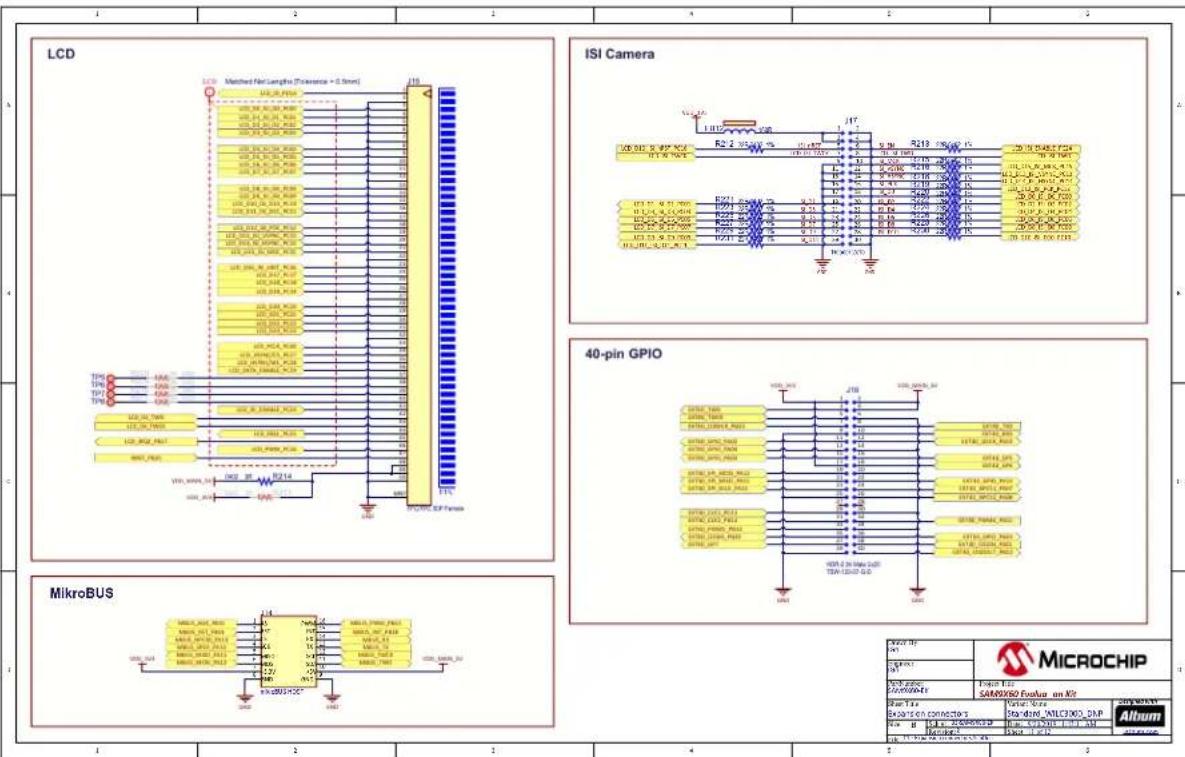
text_image
LCD Matched Net Length (Tolerance = 0.5mm) LCD 120.00.0000 120.00.0000 120.00.0000 120.00.0000 120.00.0000 120.00.0000 120.00.0000 120.00.0000 120.00.0000 121.37.38.39.39.39.39.39.39.39.39.39.39.39.39.39.39.39.39.39.39.39.39.39.39.39.39.39.39.39.39.39.39.39.39.39.39 121.37.38.39.39.39.39.39.39.39.39.39.39.39.39.39.39.39.39.39.39.39.39.39.39 121.37.38.39.39.39.39.39.39.39.38 121.37.38.39.39.39.39.39.39.39.39.39.39.39.39 121.37.38.39.39.39.39.38 121.37.38.39.39.39.38 121.37.38.39.38 121.37.38.38 121.37.38 121. 121. 121. 121. 121. 121. 121. 121. 121. 121. 121. 121. 121. 121. 121. 121. 121. 121. 121. 121. 121. 121. 121. 121. 121. 121 121. 121. 121. 121. 121. 121. 121. 121. 121. 121. 121. 121. 121. 121. 121. 121. 121. 121. 121. 121. 121. 121. 121. 121. 124 64 64 64 64 64 64 64 64 64 64 64 64 64 64 64 64 64 64 64 64 64 64 64 64 64 64 64 64 64 64 64 64 64 65 65 65 65 65 65 65 65 65 65 65 65 65 65 65 65 65 65 65 65 65 65 65 65 65 65 65 65 65 65 65 65 65 65Figure 6-12. User Interaction

text_image
USER PUSH BUTTONS RGB LEDs DISABLE BOOT JTAG FTDI DEBUG PLACEHOLDERS PAD1 PAD2 CRC FCL2 FCL3 MicroCHIP SAMS9850 Epsilon on Kit User Microchip Standard 076/0830 DkV Altum R100 0.1 0.2 0.3 0.4 0.5 0.6 0.7 0.8 0.9 1.0 1.1 1.2 1.3 1.4 1.5 1.6 1.7 1.8 1.9 2.0 2.1 2.2 2.3 2.4 2.5 2.6 2.7 2.8 2.9 3.0 3.1 3.2 3.3 3.4 3.5 3.6 3.7 3.8 3.9 4.0 4.1 4.2 4.3 4.4 4.5 4.6 4.7 4.8 4.9 5.0 5.1 5.2 5.3 5.4 5.5 5.6 5.7 5.8 5.9 6.0 6.1 6.2 6.3 6.4 6.5 6.6 6.7 6.8 6.9 7.0 LASE: LSE PACD: PACD-PC MOS: MOS-PC USB: USB-PC CNC: CNC-PC COS: COS-PC COS: COS-PC COS: COS-PC COS: COS-PC COS: COS-PC COS: COS-PC COS: COS-PC COS: COS-PC COS: COS-PC COS: COS-PC COS: COS-PC COS: COS-PC COS: COS-PC PACD: PACD-PC MOS: MOS-PC USB: USB-PC CNC: CNC-PC COS: COS-PC COS: COS-PC COS: COS-PC COS: COS-PC COS: COS-PC COS: COS-PC COS: COS-PC COS: COS-PC COS: PACD: PACD: MOS: MOS-PC USB: USB-PC CNC: CNC-PC COS: COS-PC COS: COS-PC COS: COS-PC COS: COS-PC COS: COS-PC COS: COS-PC COS: COS-PC COS: COS-PC COS: COS-PC COS: COS- PACD: PACD: MOS: MOS-PC USB: USB-PC CNC: CNC-PC COS: COS-PC COS: COS-PC COS: COS-PC COS: COS-PC COS: COS-PC COS: COS-PC COS: COS-PC COS: COS-PC COS: COS- PACD: PACD: MOS: MOS-PC USB: MOS-PC CNC: CNC-PC COS: CCS-PC COS: CCS-PC COS: CCS-PC COS: CCS-PC COS: CCS-PC COS: CCS-PC COS: CCS-PC COS: CCS-PC COS: CCS-PC COS: CCS-PC COS: CCS-PC COS: CCS-PC COS: CCS-PC PACD: PACD: MOS: MOS-PC USB: MDS-PC CNC: CNC-PC COS: CDS-PC COS: CDS-PC COS: CDS-PC COS: CDS-PC COS: CDS-PC COS: CDS-PC COS: CDS-PC COS: CDS-PC COS: CDS-PC COS: CDS-PC COS: CDS-PC COS: CDS-PC COS: CDS-PC PACD: PACD: MOS: MDS-PC USB: MDS-PC CNC: MDS-PC COS: MDS-PC COS: MDS-PC COS: MDS-PC COS: MDS-PC COS: MDS-PC COS: MDS-PC COS: MDS-PC COS: MDS- PACD: PACD: MOS: MDS-PC USB: MDS-PC CNC: MDS-PC COS: MDS-PC COS: MDS-PC COS: MDS-PC COS: MDS-PC COS: MDS- PACD: PACD: MOS: MDS-PC USB: MDS-PC CNC: MDS-PC COS: MDS-PC COS: MDS-PC COS: MDS-PC TPO: TPO: TPO: TPO: TPO: TPO: TPO: TPO: TPO: TPO: TPO: TPO: TPO: TPO: TPO: TPO: TPO: TPO: TPO: TPO: TPO: TPO: TPO: TPO: TPO: TPO: TPO: TPO: TPO: TPO: TPO: TPO: TPO: TPO: USS: USS: USS: USS: USS: USS: USS: USS: USS: USS: USS: USS: USS: USS: USS: USS: USS: USS: USS: USS: USS: USS: USS: USS: USS: USS: USS: USS: USS: USS: USS: USS: USS: USS:Figure 6-13. On-board J-Link
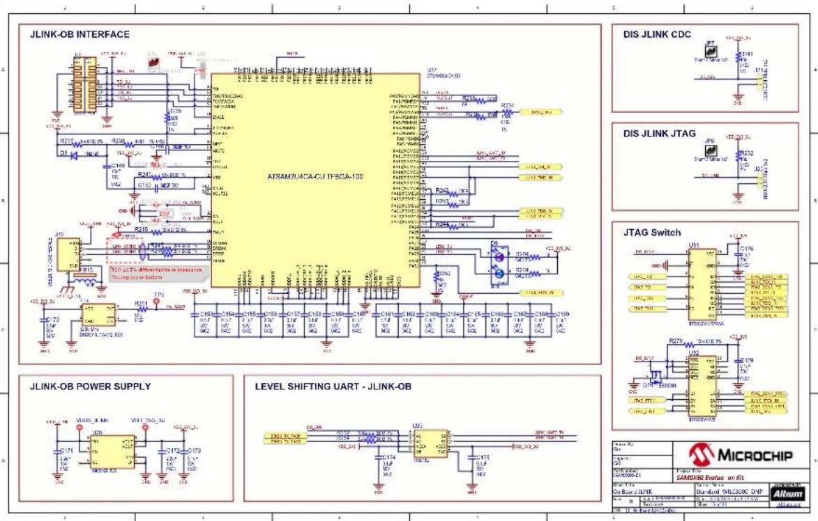
text_image
JLINK-OB INTERFACE ATSAM3U4CA-CUI IFBCA-100 DIS JLINK CDC DIS JLINK JTAG JTAG Switch JLINK-OB POWER SUPPLY LEVEL SHIFTING UART - JLINK-OB MICROCHIP On Board JLINK Standard MICR2000 DVP Altum SAMS2000000000000000000000000000000000000000000000000000000000000000000000000000000000000000000 VDD 75 1.2V 1.2V 1.2V 1.2V 1.2V 1.2V 1.2V 1.2V 1.2V 1.2V 1.2V 1.2V 1.2V 1.2V 1.2V 1.2V 1.2V 1.2V 1.2V 1.2V 1.2 R317 R326 R335 R345 R355 R365 R375 R385 R395 R405 R415 R425 R435 R445 R455 R465 R475 R485 R495 R505 R515 R525 R535 R545 R555 R565 R575 R585 R595 R605 R615 R625 R635 R645 R655 R665 R675 R685 R695 R705 R715 R725 R735 R745 R755 R765 R775 R785 R795 R805 R815 R825 R835 R845 R855 R865 R875 R885 R895 R905 R915 R925 R935 R945 R955 R965 R975 R985 R995 R1007. Revision History
Microchip provides online support via our website at http://www.microchip.com/. This website is used to make files and information easily available to customers. Some of the content available includes:
- Product Support – Data sheets and errata, application notes and sample programs, design resources, user's guides and hardware support documents, latest software releases and archived software
- General Technical Support – Frequently Asked Questions (FAQs), technical support requests, online discussion groups, Microchip design partner program member listing
- Business of Microchip – Product selector and ordering guides, latest Microchip press releases, listing of seminars and events, listings of Microchip sales offices, distributors and factory representatives
Product Change Notification Service
Microchip's product change notification service helps keep customers current on Microchip products. Subscribers will receive email notification whenever there are changes, updates, revisions or errata related to a specified product family or development tool of interest.
To register, go to http://www.microchip.com/pcn and follow the registration instructions.
Customer Support
Users of Microchip products can receive assistance through several channels:
• Distributor or Representative
- Local Sales Office
- Embedded Solutions Engineer (ESE)
- Technical Support
Customers should contact their distributor, representative or ESE for support. Local sales offices are also available to help customers. A listing of sales offices and locations is included in this document.
Technical support is available through the website at: http://www.microchip.com/support
Microchip Devices Code Protection Feature
Note the following details of the code protection feature on Microchip devices:
- Microchip products meet the specification contained in their particular Microchip Data Sheet.
- Microchip believes that its family of products is one of the most secure families of its kind on the market today, when used in the intended manner and under normal conditions.
- There are dishonest and possibly illegal methods used to breach the code protection feature. All of these methods, to our knowledge, require using the Microchip products in a manner outside the operating specifications contained in Microchip's Data Sheets. Most likely, the person doing so is engaged in theft of intellectual property.
- Microchip is willing to work with the customer who is concerned about the integrity of their code.
- Neither Microchip nor any other semiconductor manufacturer can guarantee the security of their code. Code protection does not mean that we are guaranteeing the product as “unbreakable.”
Code protection is constantly evolving. We at Microchip are committed to continuously improving the code protection features of our products. Attempts to break Microchip's code protection feature may be a violation of the Digital Millennium Copyright Act. If such acts allow unauthorized access to your software or other copyrighted work, you may have a right to sue for relief under that Act.
Legal Notice
Information contained in this publication regarding device applications and the like is provided only for your convenience and may be superseded by updates. It is your responsibility to ensure that your application meets with
your specifications. MICROCHIP MAKES NO REPRESENTATIONS OR WARRANTIES OF ANY KIND WHETHER EXPRESS OR IMPLIED, WRITTEN OR ORAL, STATUTORY OR OTHERWISE, RELATED TO THE INFORMATION, INCLUDING BUT NOT LIMITED TO ITS CONDITION, QUALITY, PERFORMANCE, MERCHANTABILITY OR FITNESS FOR PURPOSE. Microchip disclaims all liability arising from this information and its use. Use of Microchip devices in life support and/or safety applications is entirely at the buyer's risk, and the buyer agrees to defend, indemnify and hold harmless Microchip from any and all damages, claims, suits, or expenses resulting from such use. No licenses are conveyed, implicitly or otherwise, under any Microchip intellectual property rights unless otherwise stated.
Trademarks
The Microchip name and logo, the Microchip logo, Adaptec, AnyRate, AVR, AVR logo, AVR Freaks, BesTime, BitCloud, chipKIT, chipKIT logo, CryptoMemory, CryptoRF, dsPIC, FlashFlex, flexPWR, HELDO, IGLOO, JukeBlox, KeeLoq, Kleer, LANCheck, LinkMD, maXStylus, maXTouch, MediaLB, megaAVR, Microsemi, Microsemi logo, MOST, MOST logo, MPLAB, OptoLyzer, PackeTime, PIC, picoPower, PICSTART, PIC32 logo, PolarFire, Prochip Designer, QTouch, SAM-BA, SenGenuity, SpyNIC, SST, SST Logo, SuperFlash, Symmetricom, SyncServer, Tachyon, TempTrackr, TimeSource, tinyAVR, UNI/O, Vectron, and XMEGA are registered trademarks of Microchip Technology Incorporated in the U.S.A. and other countries.
APT, ClockWorks, The Embedded Control Solutions Company, EtherSynch, FlashTec, Hyper Speed Control, HyperLight Load, IntelliMOS, Libero, motorBench, mTouch, Powermite 3, Precision Edge, ProASIC, ProASIC Plus, ProASIC Plus logo, Quiet-Wire, SmartFusion, SyncWorld, Temux, TimeCesium, TimeHub, TimePictra, TimeProvider, Vite, WinPath, and ZL are registered trademarks of Microchip Technology Incorporated in the U.S.A.
Adjacent Key Suppression, AKS, Analog-for-the-Digital Age, Any Capacitor, AnyIn, AnyOut, BlueSky, BodyCom, CodeGuard, CryptoAuthentication, CryptoAutomotive, CryptoCompanion, CryptoController, dsPICDEM, dsPICDEM.net, Dynamic Average Matching, DAM, ECAN, EtherGREEN, In-Circuit Serial Programming, ICSP, INICnet, Inter-Chip Connectivity, JitterBlocker, KleerNet, KleerNet logo, memBrain, Mindi, MiWi, MPASM, MPF, MPLAB Certified logo, MPLIB, MPLINK, MultiTRAK, NetDetach, Omniscient Code Generation, PICDEM, PICDEM.net, PICkit, PICtail, PowerSmart, PureSilicon, QMatrix, REAL ICE, Ripple Blocker, SAM-ICE, Serial Quad I/O, SMART-I.S., SQI, SuperSwitcher, SuperSwitcher II, Total Endurance, TSHARC, USBCheck, VariSense, ViewSpan, WiperLock, Wireless DNA, and ZENA are trademarks of Microchip Technology Incorporated in the U.S.A. and other countries.
SQTP is a service mark of Microchip Technology Incorporated in the U.S.A.
The Adaptec logo, Frequency on Demand, Silicon Storage Technology, and Symmcom are registered trademarks of Microchip Technology Inc. in other countries.
GestIC is a registered trademark of Microchip Technology Germany II GmbH & Co. KG, a subsidiary of Microchip Technology Inc., in other countries.
All other trademarks mentioned herein are property of their respective companies.
© 2020, Microchip Technology Incorporated, Printed in the U.S.A., All Rights Reserved.
ISBN: 978-1-5224-5460-1
AMBA, Arm, Arm7, Arm7TDMI, Arm9, Arm11, Artisan, big.LITTLE, Cordio, CoreLink, CoreSight, Cortex, DesignStart, DynamlQ, Jazelle, Keil, Mali, Mbed, Mbed Enabled, NEON, POP, RealView, SecurCore, Socrates, Thumb, TrustZone, ULINK, ULINK2, ULINK-ME, ULINK-PLUS, ULINKpro, μVision, Versatile are trademarks or registered trademarks of Arm Limited (or its subsidiaries) in the US and/or elsewhere.
Quality Management System
For information regarding Microchip's Quality Management Systems, please visit http://www.microchip.com/quality.
Worldwide Sales and Service
AMERICAS ASIA/PACIFIC ASIA/PACIFIC EUROPE
| Corporate Office2355 West Chandler Blvd.Chandler, AZ 85224-6199Tel: 480-792-7200Fax: 480-792-7277Technical Support:http://www.microchip.com/supportWeb Address:http://www.microchip.comAtlantaDuluth, GATel: 678-957-9614Fax: 678-957-1455Austin, TXTel: 512-257-3370BostonWestborough, MATel: 774-760-0087Fax: 774-760-0088ChicagoItasca, ILTel: 630-285-0071Fax: 630-285-0075DallasAddison, TXTel: 972-818-7423Fax: 972-818-2924DetroitNovi, MITel: 248-848-4000Houston, TXTel: 281-894-5983IndianapolisNoblesville, INTel: 317-773-8323Fax: 317-773-5453Tel: 317-536-2380Los AngelesMission Viejo, CATel: 949-462-9523Fax: 949-462-9608Tel: 951-273-7800Raleigh, NCTel: 919-844-7510New York, NYTel: 631-435-6000San Jose, CASel: 408-735-9110Tel: 408-436-4270Canada - TorontoTel: 905-695-1980Fax: 905-695-2078 | Australia - SydneyTel: 61-2-9868-6733China - BeijingTel: 86-10-8569-7000China - ChengduTel: 86-28-8665-5511China - ChongqingTel: 86-23-8980-9588China - DongguanTel: 86-769-8702-9880China - GuangzhouTel: 86-20-8755-8029China - HangzhouTel: 86-571-8792-8115China - Hong Kong SARTel: 852-2943-5100China - NanjingTel: 86-25-8473-2460China - QingdaoTel: 86-532-8502-7355China - ShanghaiTel: 86-21-3326-8000China - ShenyangTel: 86-24-2334-2829China - ShenzhenTel: 86-755-8864-2200China - SuzhouTel: 86-186-6233-1526China - WuhanTel: 86-27-5980-5300China - XianTel: 86-29-8833-7252China - XiamenTel: 86-592-2388138China - ZhuhaiTel: 86-756-3210040 | India - BangaloreTel: 91-80-3090-4444India - New DelhiTel: 91-11-4160-8631India - PuneTel: 91-20-4121-0141Japan - OsakaTel: 81-6-6152-7160Japan - TokyoTel: 81-3-6880-3770Korea - DaeguTel: 82-53-744-4301Korea - SeoulTel: 82-2-554-7200Malaysia - Kuala LumpurTel: 60-3-7651-7906Malaysia - PenangTel: 60-4-227-8870Philippines - ManilaTel: 63-2-634-9065SingaporeTel: 65-6334-8870Taiwan - Hsin ChuTel: 886-3-577-8366Taiwan - KaohsiungTel: 886-7-213-7830Taiwan - TaipeiTel: 886-2-2508-8600Thailand - BangkokTel: 66-2-694-1351Vietnam - Ho Chi MinhTel: 84-28-5448-2100 | Austria - WelsTel: 43-7242-2244-39Fax: 43-7242-2244-393Denmark - CopenhagenTel: 45-4450-2828Fax: 45-4485-2829Finland - EspooTel: 358-9-4520-820France - ParisTel: 33-1-69-53-63-20Fax: 33-1-69-30-90-79Germany - GarchingTel: 49-8931-9700Germany - HaanTel: 49-2129-3766400Germany - HeilbronnTel: 49-7131-72400Germany - KarlsruheTel: 49-721-625370Germany - MunichTel: 49-89-627-144-0Fax: 49-89-627-144-44Germany - RosenheimTel: 49-8031-354-560Israel - Ra'ananaTel: 972-9-744-7705Italy - MilanTel: 39-0331-742611Fax: 39-0331-466781Italy - PadovaTel: 39-049-7625286Netherlands - DrunenTel: 31-416-690399Fax: 31-416-690340Norway - TrondheimTel: 47-72884388Poland - WarsawTel: 48-22-3325737Romania - BucharestTel: 40-21-407-87-50Spain - MadridTel: 34-91-708-08-90Fax: 34-91-708-08-91Sweden - GothenbergTel: 46-31-704-60-40Sweden - StockholmTel: 46-8-5090-4654UK - WokinghamTel: 44-118-921-5800Fax: 44-118-921-5820 |