SY88353BL - Amplifier Microchip - Free user manual and instructions
Find the device manual for free SY88353BL Microchip in PDF.

User questions about SY88353BL Microchip
0 question about this device. Answer the ones you know or ask your own.
Ask a new question about this device
Download the instructions for your Amplifier in PDF format for free! Find your manual SY88353BL - Microchip and take your electronic device back in hand. On this page are published all the documents necessary for the use of your device. SY88353BL by Microchip.
USER MANUAL SY88353BL Microchip
The SY88353BL limiting post amplifier is designed for use in fiber-optic receivers, and is specially optimized for WDM applications where optical amplifiers such as EDFAs and Raman amplifier are used. The device connects to typical transimpedance amplifiers (TIAs). The linear signal from TIAs can contain significant amounts of noise that is unevenly distributed between top and bottom rails due to the ASE noise generated by the optical amplifiers, crosstalk, or non-linear effect in the fiber. In order to optimize the BER in such noisy conditions, the decision threshold between bit 1 and bit 0, needs to be moved to the rail that contains less noise. The SY88353BL features a pin at which an external voltage can be applied to move the crossing point up and down, from 20% to 80%, for BER optimization purposes.
The SY88353BL operates from a single +3.3V power supply, over temperatures ranging from -40^ to +85^ . Signals with data rates from 155Mbps up to 3.2Gbps, and as small as 10mV_pp , can be amplified to drive devices with CML or PECL inputs.
The SY88353L features a Loss-of-Signal (LOS) open-collector TTL output. A programmable Loss-of-Signal level set pin (LOS LVL ) sets the sensitivity of the input amplitude detection. LOS asserts high if the input amplitude falls below the threshold sets by LOS LVL and de-asserts low otherwise. The enable bar input (/EN) de-asserts the true output signal without removing the input signal. The LOS output can be fed back to the /EN input to maintain output stability under a loss-of-signal condition. Typically, 3.3dB LOS hysteresis is provided to prevent chattering.
All support documentation can be found on Micrel's web site at: www.micrel.com.
Features
- Single 3.3V power supply
- Fast LOS release/assert
• 155Mbps to 3.2Gbps operation - Low-noise CML data outputs
- Chatter-free Open-Collector TTL loss-of-signal (LOS) output
- TTL /EN input
- Programmable LOS level set (LOS _LVL )
• Programmable Decision Threshold
• Available in a tiny 3mm x 3mm MLF ^® package
Applications
- WDM Systems
• Gigabit Ethernet, 1X and 2X Fibre Channel
• SONET/SDH: OC-3/12/24/48 – STM1/4/8/16 - Low-gain TIA interface
Markets
- Datacom/telecom
• Optical transceiver
MLF and MicroLeadFrame are registered trademarks of Amkor Technology.
Micrel Inc. • 2180 Fortune Drive • San Jose, CA 95131 • USA • tel +1 (408) 944-0800 • fax +1 (408) 474-1000 • http://www.micrel.com
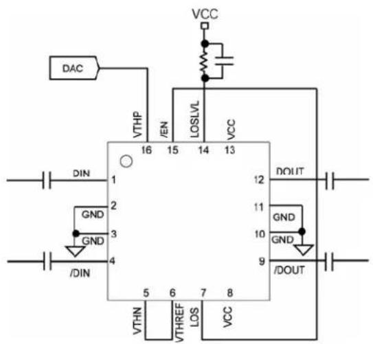
Typical Application Circuit
text_image
VCC DAC VIN EN LOSLVL VTHP 16 15 14 13 DIN 1 2 GND 3 GND /DIN 4 5 6 7 8 VTHN VTHREF LOS VCC 12 DOUT 11 GND 10 GND 9 /DOUTProgrammable Decision Threshold
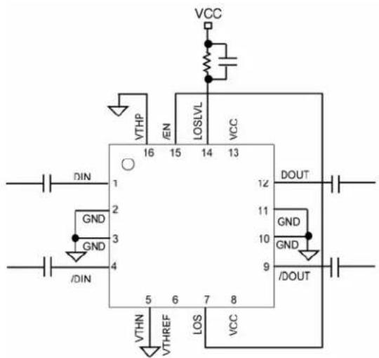
text_image
VCC VIN EN LOSLVL VCC 16 15 14 13 DIN 1 2 GND 3 GND 4 /DIN 5 6 7 8 VTHN VTHREF LOS VCC 12 DOUT 11 GND 10 GND 9 /DOUTFixed Decision Threshold
Ordering Information
| Part Number | Package Type | Operating Range | Package Marking | Lead Finish |
| SY88353BLMG | MLF-16 | Industrial | 353B with Pb-Free bar line indicator | NiPdAu Pb-Free |
| SY88353BLMGTR ^(1) | MLF16 Industrial | 353B with Pb-Free bar line indicator | NiPdAu Pb-Free |
Note:
1. Tape and Reel.
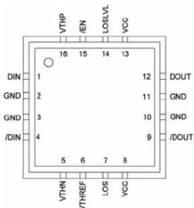
Pin Configuration
text_image
VTHP IEN LOSLVL VCC 16 15 14 13 12 DIN 1 GND 2 GND 3 /DIN 4 5 6 7 8 VTHN VTHREF LOS VCC 11 GND GND /DOUT16-Pin MLF ^® (MLF-16)
Pin Description
| Pin Number | Pin Name Type | Pin Function | |
| 1 DIN Data Input True data input. | |||
| 4 /DIN Data Input Complementary data input. | |||
| 5 | VTHN | DC | Tie this pin pin 6 (VTHREF) and apply a DC voltage on pin 16 (VTHP) for signal crossing adjustment. Connect to ground if no crossing adjustment is needed. |
| 6 | VTHREF | 1.25V Reference voltage (referenced to ground) for decision threshold adjustment. | |
| 7 | LOS | Open-collector TTL output | Loss-of-Signal: asserts high when the data input amplitude falls below the threshold set by LOS_LVL . |
| 9 /DOUT | CML Output | Complementary data output. | |
| 12 | DOUT | CML Output True data output. | |
| 14 | LOSLVL | Input | Loss-of-Signal Level Set. A resistor from this pin to V_CC sets the threshold for the data input amplitude at which LOS will be asserted. |
| 15 | /EN | TTL Input: Default is HIGH. | /Enable: This input enables the outputs when it is LOW. Note that this input is internally connected to a 25kΩ pull-up resistor and will default to a logic HIGH state if left open. |
| 16 | VTHP | DC Input | Apply a DC voltage from 0 to 2.4V to adjust the signal crossing level when pin 5 (VTHN) is tied to pin 6 (VTHREF). 1.25V sets the crossing close to 50%. Connect to ground if no crossing adjustment is needed. |
| 2, 3, 10, 11 GND | Ground Device ground. | ||
| 8, 13 VCC | Power Supply Positive power supply. | ||
Absolute Maximum Ratings ^(1)
Supply Voltage ( V_cc ) 0V to +4.0V
Input Voltage (DIN, /DIN) 0 to V_cc
Output Current ( I_OUT ) Continuous....±25mA
/EN Voltage ....0 to V_cc
V_REF Current -800 A to +500 A
LOS_LVL Voltage.... V_REF to V_CC
Lead Temperature (soldering, 20sec.)....+260°C
Storage Temperature ( T_s ) -65^ to +150^
Operating Ratings ^(2)
Supply Voltage ( V_cc )....+3.0V to +3.6V
Ambient Temperature ( T_A ) -40^ to +85^
Junction Temperature ( T_J ) -40^ to +120^
Supply Voltage (Vcc) +3.0V to +3.6V
Ambient Temperature ( T_A )....-40°C to +85°C
Package Thermal Resistance ^(3) MLF ^®
( JA)0Still-air 60°C/W
(B) 33°C/W
DC Electrical Characteristics
V_CC = 3.0 to 3.6V; T_A = -40^ to +85^, typical values at V_CC = 3.3V, T_A = 25^.
| Symbol | Parameter Condition | Min | Typ | Max | Units | |||
| I_CC | Power Supply Current | No output load | 45 | 62 | mA | |||
| LOS_LVL | LOS_LVL Voltage | V_CC-1.3 | V_CC | V | ||||
| V_OH | DOUT, /DOUT HIGH Voltage | V_CC-0.020 | V_CC-0.005 | V_CC | V | |||
| V_OL | DOUT, /DOUT LOW Voltage | V_CC-0.475 | V_CC-0.400 | V_CC-0.350 | V | |||
| V_OFFSET | Differential Output Offset | ±80 | mV | |||||
| V_THREF | Decision Threshold Reference Voltage | 1.25 | V | |||||
| Z_0 | Single-Ended Output Impedance | 40 | 50 | 60 | Ω | |||
| Z_1 | Single-Ended Input Impedance | 40 | 50 | 60 | Ω | |||
TTL DC Electrical Characteristics
V_CC = 3.0 to 3.6V; T_A = -40^ to +85^, typical values at V_CC = 3.3V, T_A = 25^.
| Symbol | Parameter | Condition | Min | Typ | Max | Units |
| Output signal Crossing Range Lower Limit | VTHN connected to VTHREF and 0-2.4V applied to VTHP. | 20 | % | |||
| Output signal Crossing Range Upper Limit | 20 ≤ DIN ≤ 100(mVpp) , see Figure on page 6. | 80 | % | |||
| V_IH | /EN Input HIGH Voltage | 2.0 | V | |||
| V_IL | /EN Input LOW Voltage | 0.8 | V | |||
| I_IH | /EN Input HIGH Current | V_IN = 2.7V V_IN = V_CC | 20100 | μAμA | ||
| I_IL | /EN Input LOW Current | V_IN = 0.5V | -0.3 | mA | ||
| I_CEX | LOS Output Leakage Current | V_OUT = V_CC | 100 | μA | ||
| V_OL | LOS Output LOW Level | Sinking 2mA | 0.5 | V |
AC Electrical Characteristics
V_CC = 3.0 to 3.6V; R_Load = 50 to V_CC; T_A = -40^ to +85^, typical values at V_CC = 3.3V, T_A = 25^.
| Symbol | Parameter Condition | Min Typ Max | Units | |||
| t_r, t_f | Output Rise/Fall Time(20% to 80%) | Note 4 60 100 | ps | |||
| t_JITTER | Deterministic Random | Note 5 Note 6 | 15 5 | ps_PP ps_RMS | ||
| V_ID Differential Input Voltage Swing 20 1800 mV | PP | |||||
| V_OD | Differential Output Voltage Swing | Note 4 | 700 | 800 950 | mV_PP | |
| T_OFF | LOS Release Time | Note 9 | 2 | 10 | μs | |
| T_ON | LOS Assert Time | Note 9 | 2 | 10 | μs | |
| LOS_AL | Low LOS Assert Level | R_LOSLVL=15kΩ, Note 7 | 9 | mV_PP | ||
| LOS_DL | Low LOS De-assert Level | R_LOSLVL=15kΩ, Note 7 | 13 | mV_PP | ||
| HYS_L | Low LOS Hysteresis | R_LOSLVL=15kΩ, Note 8 | 3.2 | dB | ||
| LOS_AM | Medium LOS Assert Level | R_LOSLVL=5kΩ, Note 7 | 17 | mV_PP | ||
| LOS_DM | Medium LOS De-assert Level | R_LOSLVL=5kΩ, Note 7 | 25 | mV_PP | ||
| HYS_M | Medium LOS Hysteresis | R_LOSLVL=5kΩ, Note 8 | 3.3 | dB | ||
| LOS_AH | High LOS Assert Level | R_LOSLVL=100Ω, Note 7 | 47 | mV_PP | ||
| LOS_DH | High LOS De-assert Level | R_LOSLVL=100Ω, Note 7 | 70 | mV_PP | ||
| HSY_H | High LOS Hysteresis | R_LOSLVL=100Ω, Note 8 | 3.4 | dB | ||
| B_-3dB | 3dB Bandwidth | 2.0 | GHz | |||
| A_V(Diff) | Differential Voltage Gain | 38 | dB | |||
| S_21 | Single-Ended Small-Signal Gain | 26 | 32 | dB | ||
Notes:
- Permanent device damage may occur if absolute maximum ratings are exceeded. This is a stress rating only and functional operation is not implied at conditions other than those detailed in the operational sections of this data sheet. Exposure to absolute maximum ratings conditions for extended periods may affect device reliability.
- The data sheet limits are not guaranteed if the device is operated beyond the operating ratings.
- Package Thermal Resistance assumes exposed pad is soldered (or equivalent) to the devices most negative potential on the PCB. _JB uses a 4-layer and _JA in still-air number, unless otherwise stated.
- Amplifier in limiting mode. Input is a 200MHz square wave.
- Deterministic jitter measured using 2.5Gbps K28.5 pattern, V_ID = 10mV_PP
- Random jitter measured using 2.5Gbps K28.7 pattern, V_ID = 10mV_PP
- See "Typical Operating Characteristics" for a graph showing how to choose a particular R_LOSLVL for a particular LOS assert and its associated de-assert amplitude.
- This specification defines electrical hysteresis as 20log (LOS De-Assert/LOS Assert). The ratio between optical hysteresis and electrical hysteresis is found to vary between 1.5 and 2, depending upon the level of received optical power and ROSA characteristics. Based upon that ratio, the optical hysteresis corresponding to the electrical hysteresis range 1dB-4.5 dB, shown in the AC characteristics table, will be 0.5dB-3dB Optical Hysteresis.
- In real world applications, the LOS Release/Assert time can be strongly influenced by the RC time constant of the AC-coupling cap and the 50Ω input termination. To keep this time low, use a decoupling cap with the lowest value that is allowed by the data rate and the number of consecutive identical bits in the application. Typical values are in the range of 0.001μF to 1.0μF.
Typical Operating Characteristics
V_CC = 3.3V, T_A = 25^, R_L = 50 to V_CC-2V , unless otherwise stated.

line
| V_THP (V) | CRCSSING (%) | | --------- | ------------ | | 1.0 | 80 | | 1.1 | 70 | | 1.2 | 60 | | 1.3 | 50 | | 1.4 | 40 | | 1.5 | 30 |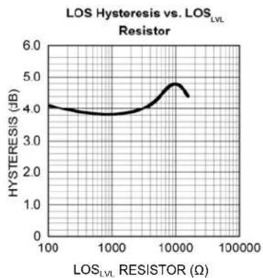
line
| LOS_LVL RESISTOR (Ω) | HYSTERESIS (dB) | | ------------------- | ---------------- | | 100 | 4.0 | | 1000 | 3.8 | | 10000 | 4.5 | | 100000 | 4.2 |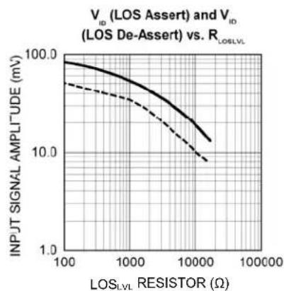
line
| LOS_LVL RESISTOR (Ω) | V_ID (LOS Assert) | V_ID (LOS De-Assert) | | --------------------- | ------------------ | -------------------- | | 100 | 100.0 | 50.0 | | 1000 | 50.0 | 25.0 | | 10000 | 10.0 | 5.0 | | 100000 | 5.0 | 2.5 |Functional Characteristics
V_CC = 3.3V, T_A = 25^, R_L = 50 to V_CC-2V, unless otherwise stated.
line
| Time (80ps/div.) | Voltage Level | | ---------------- | ------------- | | 0 | 1 Level | | 1 | 9 Level | | 2 | 0 Level |
text_image
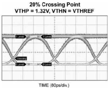
50% Crossing Point VTHP = 1.25V, VTHN = VTHREF 1 Level 2 Level Crossing 3 Level 4 Level TIME (80ps/div.)
line
| Time (80ps/div.) | Voltage Level | | ---------------- | ------------- | | 0 | 0 | | 1 | 1 | | 2 | 0 | | 3 | 1 | | 4 | 0 | | 5 | 1 | | 6 | 0 | | 7 | 1 | | 8 | 0 | | 9 | 1 | | 10 | 0 | | 11 | 1 | | 12 | 0 | | 13 | 1 | | 14 | 0 | | 15 | 1 | | 16 | 0 | | 17 | 1 | | 18 | 0 | | 19 | 1 | | 20 | 0 | | 21 | 1 | | 22 | 0 | | 23 | 1 | | 24 | 0 | | 25 | 1 | | 26 | 0 | | 27 | 1 | | 28 | 0 | | 29 | 1 | | 30 | 0 | | 31 | 1 | | 32 | 0 | | 33 | 1 | | 34 | 0 | | 35 | 1 | | 36 | 0 | | 37 | 1 | | 38 | 0 | | 39 | 1 | | 40 | 0 | | 41 | 1 | | 42 | 0 | | 43 | 1 | | 44 | 0 | | 45 | 1 | | 46 | 0 | | 47 | 1 | | 48 | 0 | | 49 | 1 | | 50 | 0 | | 51 | 1 | | 52 | 0 | | 53 | 1 | | 54 | 0 | | 55 | 1 | | 56 | 0 | | 57 | 1 | | 58 | 0 | | 59 | 1 | | 60 | 0 | | 61 | 1 | | 62 | 0 | | 63 | 1 | | 64 | 0 | | 65 | 1 | | 66 | 0 | | 67 | 1 | | 68 | 0 | | 69 | 1 | | 70 | 0 | | 71 | 1 | | 72 | 0 | | 73 | 1 | | 74 | 0 | | 75 | 1 | | 76 | 0 | | 77 | 1 | | 78 | 0 | | 79 | 1 | | 80 | 0 |Functional Block Diagram
text_image
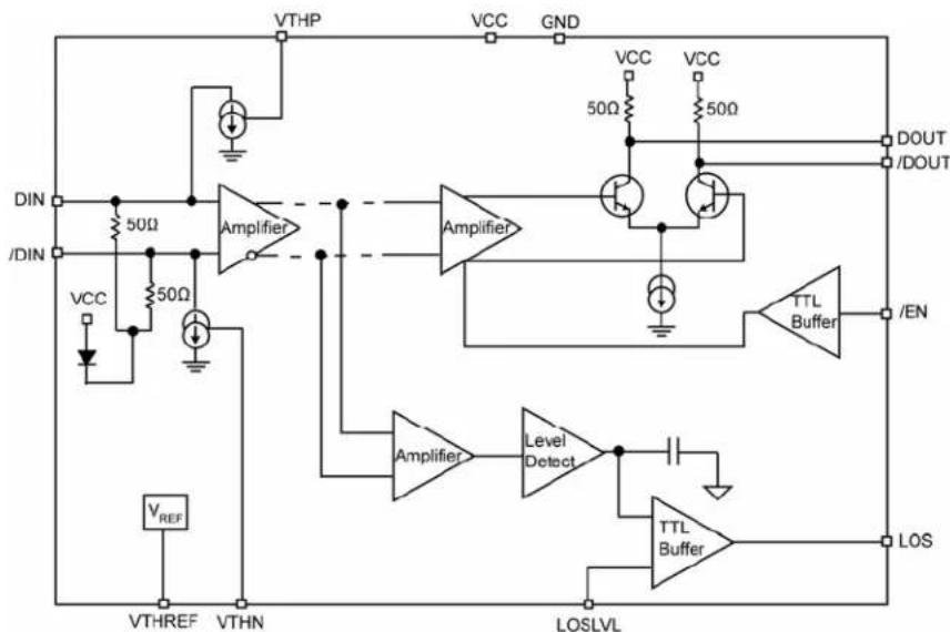
VTHP VCC GND DIN 50Ω Amplifier VCC 50Ω /DIN VCC 50Ω VREF VTHREF VTHN Amplifier 50Ω VCC 50Ω DOUT /OUT TTL Buffer /EN Amplifier Level Detect TTL Buffer LOS LOSLVLDetailed Description
The SY88353L limiting post amplifier operates from a single +3.3V power supply, over temperatures from -40°C to +85°C. Signals with data rates from 155Mbps up to 3.2Gbps, and as small as 10mV pp , can be amplified. Figure 1 shows the allowed input voltage swing. The SY88353L generates a LOS output that can be feedback to /EN for output stability in the absence of a signal at the input. LOS LVL sets the sensitivity of the input amplitude detection. The amplifier features a signal crossing adjustment for BER optimization in optical links using optical amplifiers such in WDM applications.
Input Amplifier/Buffer
Figure 2 shows a simplified schematic of the input stage. The input amplifier allows signals as small as 10mVpp to be detected and amplified. The input amplifier allows input signals as large as 1800mVpp . Input signals are linearly amplified with a typical 38dB differential voltage gain. Since it is a limiting amplifier, the SY88353BL outputs typically 800mVpp voltage-limited waveforms for input signals that are greater than 12mVpp . Applications requiring the SY88353L to operate with high gain should have the upstream TIA placed as close as possible to the SY88353BL's input pins to ensure the best performance of the device.
Output Buffer
The SY88353BL's CML output buffer is designed to drive 50Ω lines and is internally terminated with 50Ω to Vcc. Figure 3 shows a simplified schematic of the output stage.
Loss-of-Signal
The SY88353L generates a chatter-free loss-of-signal (LOS) open-collector, TTL output, as shown in Figure 4. LOS is used to determine if the input amplitude is too small to be considered a valid input. LOS asserts high if the input amplitude falls below the threshold set by LOSLVL and de-asserts low otherwise. LOS can be fed back to the enable (/EN) input to maintain output stability under a loss of signal condition. /EN de-asserts low the true output signal without removing the input signals. Typically, 3.3dB LOS hysteresis is provided to prevent chattering.
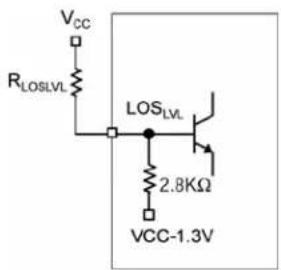
Loss-of-Signal-Level Set
A programmable LOS level set pin (LOS LVL ) sets the threshold of the input amplitude detection. Connecting an external resistor between VCC and LOS LVL sets the voltage at LOS LVL . This voltage ranges from V_CC to V_CC-1.3V . The external resistor creates a voltage divider between V_CC and V_CC-1.3V , as shown in Figure 5.
Hysteresis
The SY88353L typically provides 3.3dB LOS electrical hysteresis, which is defined as 20log (VIN LOS-De-assert /VIN LOS-Assert ). Since the relationship between the voltage out of the ROSA and optical power at its input is linear, the optical hysteresis will be typically half of the electrical hysteresis reported in the datasheet. In practice, the ratio between electrical and optical hysteresis is found to be within the range 1.5 to 1.8dB. Thus, 3.3dB electrical hysteresis will correspond to an optical hysteresis within the range 1.8 to 2.2dB.
Signal Crossing Adjustment
In order to optimize the decision threshold level and hence, the BER of the optical link, the SY88353L provides two pins for output signal crossing control. The signal crossing can be adjusted by connecting VTHN (pin 5) to VTHREF (pin 6), and applying a DC signal at VTHP (pin 16). By varying the DC signal at VTHP from -0V to 2.5V – while the input signal to the post amplifier is less than 100mVpp, the crossing of the output signal will change from 20% to 80% reaching 50% when VTHP
= VTHREF = 1.25V. If the crossing control function is not needed, VTHN and VTHP must be connected to ground.
The zero crossing vs. VTHP plot, shown on page 6, shows how the crossing of the output signal changes with the voltage applied at VTHP (pin 16) while VTHN (pin 5) is tied to VTHREF (pin 6) for different input signal levels.
other
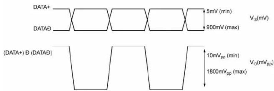
| Signal | Value | |--------|--------------| | DATA+ | 5mV (min) | | DATA+ | 900mV (max) | | DATA-D | 5mV (min) | | DATA-D | 900mV (max) | | (DATA+) D (DATAD) | 10mVpp (min) | | (DATA+) D (DATAD) | 1800mVpp (max) |Figure 1. V_IS and V_ID Definition
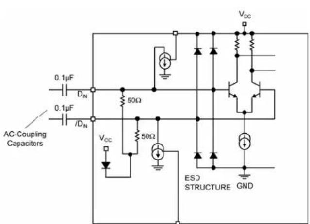
text_image
0.1μF DN 0.1μF /DN AC-Coupling Capacitors VCC 50Ω 50Ω ESD STRUCTURE GND VCCFigure 2. Input Structure
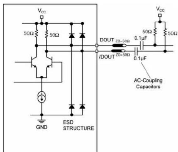
text_image
VCC 50Ω 50Ω DOUT Z0=56Ω / DOUT Z0=50Ω GND ESD STRUCTURE AC-Coupling Capacitors VCC 50Ω 50Ω 0.1μF 0.1μFFigure 3. Output Structure

Figure 4. LOS Output Structure
text_image
VCC RLOSLVL LOS LVL 2.8KΩ VCC-1.3VFigure 5. LOSLVL Setting Circuit
Note: Recommended value for RLOSLVL is 15kΩ or less.
Related Product and Support Documentation
| Part Number Function Data Sheet Link | ||
| AN-45 | Notes on Sensitivity and Hysteresis in Micrel Post Amplifiers | http://www.micrel.com/product-info/app_hints+notes.shtml |
Package Information
text_image
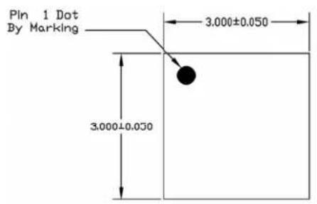
Pin 1 Dot By Marking 3.000±0.050 3.000±0.030TOP VIEW

text_image
PIN #1 IDENTIFICATION CHAMFER 0.300 X 45° 1.550±0.050 Exp. DAP 0.400±0.050 1.550±0.050 Exp. DAP 0.230±0.050 0.500 Bsc 1.500 Ref.BOTTOM VIEW

text_image
0.850±0.050 0.000-0.050 0.203±0.025SIDE VIEW
NOTE:
1. ALL DIMENSIONS ARE IN MILLIMETERS.
2. MAX. PACKAGE WARPAGE IS 0.05 mm.
3. MAXIMUM ALLOWABLE BURRS IS 0.076 nm IN ALL DIRECTIONS.
4. PIN #1 ID ON TOP WILL BE LASER/INK MARKED.
16-Pin (3mm x 3mm) MLF ^® (MLF-16)
MICREL, INC. 2180 FORTUNE DRIVE SAN JOSE, CA 95131 USA
TEL +1 (408) 944-0800 FAX +1 (408) 474-1000 WEB http://www.micrel.com
The information furnished by Micrel in this data sheet is believed to be accurate and reliable. However, no responsibility is assumed by Micrel for its use. Micrel reserves the right to change circuitry and specifications at any time without notification to the customer.
Micrel Products are not designed or authorized for use as components in life support appliances, devices or systems where malfunction of a product can reasonably be expected to result in personal injury. Life support devices or systems are devices or systems that (a) are intended for surgical implant into the body or (b) support or sustain life, and whose failure to perform can be reasonably expected to result in a significant injury to the user. A Purchaser's use or sale of Micrel Products for use in life support appliances, devices or systems is a Purchaser's own risk and Purchaser agrees to fully indemnify Micrel for any damages resulting from such use or sale.
© 2006 Micrel. Incorporated.