SY88403BL - Amplifier Microchip - Free user manual and instructions
Find the device manual for free SY88403BL Microchip in PDF.

User questions about SY88403BL Microchip
0 question about this device. Answer the ones you know or ask your own.
Ask a new question about this device
Download the instructions for your Amplifier in PDF format for free! Find your manual SY88403BL - Microchip and take your electronic device back in hand. On this page are published all the documents necessary for the use of your device. SY88403BL by Microchip.
USER MANUAL SY88403BL Microchip
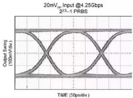
The SY88403BL is a low-power limiting post amplifier optimized for copper applications. The device connects to typical transimpedance amplifiers (TIAs). The linear signal output from TIAs can contain significant amounts of noise and may vary in amplitude over time. The SY88403BL quantizes these signals and outputs typically 800mV_PP voltage-limited waveforms.
The SY88403BL operates from a single +3.3V ±10% power supply, over an industrial temperature range of -40°C to +85°C. With its wide bandwidth and high gain, signals with data rates up to 4.25Gbps and as small as 5mV _PP can be amplified to drive devices with CML inputs or AC-coupled PECL inputs.
The SY88403BL incorporates a loss-of-signal (LOS) open-collector TTL output with internal 4.75kΩ pull-up resistor. A programmable loss-of-signal level set pin (LOSLVL) sets the sensitivity of the input amplitude detection. LOS asserts high if the input amplitude falls below the threshold set by LOSLVL and de-asserts low otherwise. LOS can be fed back to the enable bar (/EN) input to maintain output stability under a loss of signal condition. /EN de-asserts the true output signal without removing the input signal. Typically, 3.5dB LOS hysteresis is provided to prevent chattering.
All support documentation can be found on Micrel's web site at: www.micrel.com.
Typical Performance
line
| Time (50ps/div) | Output Swing (100mV/div) | | --------------- | ------------------------ | | 0 | 0 | | 50 | 0 | | 100 | 0 | | 150 | 0 | | 200 | 0 | | 250 | 0 | | 300 | 0 | | 350 | 0 | | 400 | 0 | | 450 | 0 | | 500 | 0 | | 550 | 0 | | 600 | 0 | | 650 | 0 | | 700 | 0 | | 750 | 0 | | 800 | 0 | | 850 | 0 | | 900 | 0 | | 950 | 0 | | 1000 | 0 |Features
• Multi-rate up to 4.25Gbps operation
- 5mV_PP input sensitivity
- Low noise 50 CML data outputs
- 800mV pp output swing
- 60ps edge rates
- 1ps RMS typ. random jitter
- 10ps PP typ. deterministic jitter
- Chatter-free Loss-of-Signal (LOS) output
- 3.5dB electrical hysteresis
-
OC-TTL output with internal 4.75kΩ pull-up resistor
-
Programmable LOS sensitivity using single external resistor
• Internal 50Ω data input termination
• TTL /EN input allows feedback from LOS - Wide operating range:
- Single 3.3V ±10% power supply
- Industrial temperature range: -40^ to +85^
• Available in a 10-pin EPAD-MSOP and 16-pin QFN package
Applications
• 1.062Gbps, 2.125Gbps and 4.25Gbps Fibre Channel
- Cable driver
- Small form factor (SFF) and small form factor pluggable (SFP) transceivers
• High-gain line driver and line receiver
Markets
• Copper interconnect
• Datacom and telecom
• Storage area network (SAN)
Typical Application
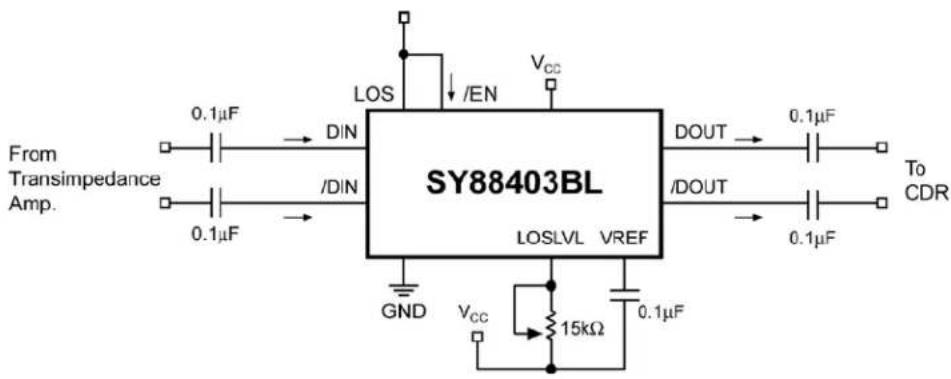
text_image
From Transimpedance Amp. 0.1µF 0.1µF DIN / DIN LOS VCC EN SY88403BL DOUT 0.1µF To CDR LOSLVL VREF GND VCC 15kΩ 0.1µFFunctional Block Diagram

flowchart
graph TD
    A["DIN 50Ω"] --> B["Limiting Amplifier"]
    C["/DIN"] --> B
    D["VREF"] --> E["VREF Generator"]
    E --> F["2.8kΩ"]
    F --> G["LOSLVL"]
    H["VCC"] --> I["CML Buffer"]
    I --> J["TTL Buffer"]
    J --> K["Level Detect"]
    K --> L["4.75kΩ"]
    L --> M["OC-TTL Buffer"]
    M --> N["LOS"]
    O["VCC 25kΩ"] --> J
    P["/EN"] --> Q["Output"]
    R["GND"] --> S["Ground"]
    T["DOUT"] --> U["Output"]
    V["DIN"] --> W["Input"]
    X["VREF"] --> Y["Input"]
Ordering Information ^(1)
| Part Number | Package Type | Operating Range | Package Marking | Lead Finish |
| SY88403BLEY | K10-2 | Industrial | 403B withPb-Free bar-line indicator | Matte-Sn |
| SY88403BLEYTR^(2) K | 10-2 Industrial | 403B with | Pb-Free bar-line indicator | Matte-Sn |
| SY88403BLMG | QFN-16 | Industrial | 403B withPb-Free bar-line indicator | NiPdAuPb-Free |
| SY88403BLMGTR^(2) | QFN-16 | Industrial | 403B withPb-Free bar-line indicator | NiPdAuPb-Free |
Notes:
1. Contact factory for die availability. Dice are guaranteed at T_A = 25^ , DC Electricals only.
2. Tape and Reel.
Pin Configuration

text_image
/EN 1 DIN 2 /DIN 3 VREF 4 LOSLVL 5 10 VCC 9 DOUT 8 /DOUT 7 LOS 6 GND10-Pin EPAD-MSOP (K10-2)

text_image
VCC IEN LOSLVL VCC 16 15 14 13 12 DOUT 1 GND 2 11 GND GND 3 10 GND /DIN 4 9 /DOUT 5 6 7 8 VCC VREF LOS VCC16-Pin QFN
Pin Description
| QFN Pin Number | EPAD-MSOP Pin Number | Pin Name | Type Pin Function | |
| 1, 4 | 2, 3 | DIN, /DIN | Differential data input | Differential data input. Each pin internally terminates to REF through 50Ω. |
| 2, 3, 10, 11 Exposed Pad | 6 Exposed Pad | GND Ground | Ground | Device ground. Exposed pad must be soldered (or equivalent) to the same potential as the ground pins. |
| 5, 8, 13, 16 | 10 VCC Power | supply | Positive power supply. Bypass with 0.1μF||0.01μF low ESR capacitors. 0.01μF capacitors should be as close as possible to VCC pin. | |
| 6 4 VREF | Reference Voltage. Bypass with 0.01μF low ESR capacitor from V_REF to V_CC to stabilize LOS_LVL and V_REF . | |||
| 7 7 LOS | Open | Collector TTL output with internal 4.75kΩ pull-up resistor | Loss-of-Signal: Asserts high when the data input amplitude falls below the threshold set by LOSLVL. | |
| 9, 12 | 9, 8 | DOUT, /DOUT | Differential CML output | Differential data output. |
| 14 | 5 | LOSLVL | Input: Default is maximum sensitivity. | Loss-of-Signal level set: A resistor from this pin to VCC sets the threshold for the data input amplitude at which the LOS output will be asserted. |
| 15 | 1 | /EN | TTL input: Default is high. | Enable bar: De-asserts true data output when high. Incorporates 25kΩ pull-up to V_CC . |
Absolute Maximum Ratings ^(1)
Supply Voltage ( V_cc ) 0V to +7.0V
/EN, LOSLVL Voltage.... 0 to Vcc
REF Current ....±1mA
LOS Current ±5mA
DOUT, /DOUT Current....±25mA
DIN, /DIN Current ....±10mA
Lead Temperature (soldering, 20sec.) ...... 260°C
Storage Temperature ( T_s ) .....-65°C to +150°C
Operating Ratings ^(2)
Supply Voltage (Vcc)....+3.0V to +3.6V
Ambient Temperature ( T_A )....-40°C to +85°C
Junction Temperature ( T_A ) ..... -40°C to +120°C
Package Thermal Resistance ^(3)
QFN
θ JA (Still-Air) 61°C/W
_JB 38°C/W
EPAD-MSOP
0 JA (Still-Air) 38°C/W
_JB 22°C/W
DC Electrical Characteristics
V_CC = +3.0V to +3.6V ; T_A = -40^ to +85^ ; typical values at V_CC = +3.3V , T_A = 25^ .
| Symbol | Parameter | Condition | Min | Typ | Max | Units |
| I_CC | Power Supply Current | 3.3V, Note 4 | 25 | 42 | mA | |
| 3.3V, Note 5 | 41 | 62 | mA | |||
| V_REF | REF Voltage | V_CC-1.3 | V | |||
| V_LOSLVL | LOSLVL Voltage Range | V_REF | V_CC | V | ||
| V_OH | DOUT, /DOUT HIGH Voltage | Note 6 | V_CC-0.020 | V_CC-0.005 | V_CC | V |
| V_OL | DOUT, /DOUT LOW Voltage | 3.3V, Note 6 | V_CC-0.475 | V_CC-0.400 | V_CC-0.350 | V |
| V_OD\_DC | DC Differential Output Voltage | Note 6 | 700 | 800 | 950 | mV |
| V_OFFSET | Differential Output Offset | ±80 | mV | |||
| Z_O | Single-Ended Output Impedance | 40 | 50 | 60 | Ω | |
| Z_I | Single-Ended Input Impedance | 40 | 50 | 60 | Ω |
TTL DC Electrical Characteristics
V_CC = +3.0V to +3.6V; T_A = -40^ to +85^.
| Symbol | Parameter | Condition | Min | Typ | Max | Units |
| V_OH | LOS Output HIGH Level | Sourcing 100μA | 2.4 | V_CC | V | |
| V_OL | LOS Output LOW Level | Sinking 2mA | 0.5 | V | ||
| V_IH | /EN Input HIGH Voltage | 2.0 | V | |||
| V_IL | /EN Input LOW Voltage | 0.8 | V | |||
| I_IH | /EN Input HIGH Current | V_IN = 2.7V V_IN = V_CC | 20100 | μAμA | ||
| I_IL | /EN Input LOW Current | V_IN = 0.5V | -0.3 | mA |
Notes:
- Permanent device damage may occur if ratings in the absolute maximum ratings section are exceeded. This is a stress rating only and functional operation is not implied for conditions other than those detailed in the operational sections of this data sheet. Exposure to absolute maximum ratings conditions for extended periods may affect device reliability.
- The data sheet limits are not guaranteed if the device is operated beyond the operating ratings.
- Thermal performance assumes are of 4-layer PCB. Exposed pad must be soldered (or equivalent) to the device's most negative potential on the PCB.
- Excludes current of CML output stage. See "Detailed Description."
- Total device current with no output load.
- Output levels are based on a 50Ω to Vcc load impedance. If the load impedance is different, the output level will be changed. Amplifier is in limiting mode. Measured at 155Mbps with 20mVpp input and PRBS-23 data pattern and 50Ω load.
AC Electrical Characteristics
V_CC = +3.0V to +3.6V ; T_A = -40^ to +85^ ; R_L = 50 to V_CC ; typical values at V_CC = +3.3V , T_A = 25^ .
| Symbol | Parameter | Condition | Min | Typ | Max | Units |
| t_r,t_f Output Rise/Fall Time(20% to 80%) | Note 7 | 60 | 120 | ps | ||
| t_JITTER | Deterministic Random | Note 8Note 9 | 10 | 1 | pS_PP pS_RMS | |
| V_ID | Differential Input Voltage Swing | See Figure 1 | 5 | 1800 | mV_pp | |
| V_OD\_AC | AC Differential Output Voltage | Note 10 | 600 | 800 | 950 | mV_pp |
| t_OFF | LOS Release Time | 2 | 10 | μs | ||
| t_ON | LOS Assert Time | 2 | 10 | μs | ||
| LOS_AL | Low LOS Assert Level | R_LOSLVL=15kΩ, Note 11 | 8 | mV_PP | ||
| LOS_DL | Low LOS De-assert Level | R_LOSLVL=15kΩ, Note 11 | 12 | mV_PP | ||
| HSY_L | Low LOS Hysteresis | R_LOSLVL=15kΩ, Note 12 | 2 | 3.5 | 4.5 | dB |
| LOS_AM | Medium LOS Assert Level | R_LOSLVL=5kΩ, Note 11 | 12 | 17 | mV_PP | |
| LOS_DM | Medium LOS De-assert Level | R_LOSLVL=5kΩ, Note 11 | 25 | 33 | mV_PP | |
| HSY_M | Medium LOS Hysteresis | R_LOSLVL=5kΩ, Note 12 | 2 | 3.5 | 4.5 | dB |
| LOS_AH | High LOS Assert Level | R_LOSLVL=100Ω, Note 11 | 34 | 47 | mV_PP | |
| LOS_DH | High LOS De-assert Level | R_LOSLVL=100Ω, Note 11 | 70 | 83 | mV_PP | |
| HSY_H | High LOS Hysteresis | R_LOSLVL=100Ω, Note 12 | 2 | 3.5 | 4.5 | dB |
| V_SR | LOS Sensitivity Range | 20 | 35 | mV_PP | ||
| A_V(Diff) | Differential Voltage Gain | 32 | 38 | dB | ||
| S_21 | Single-Ended Small-Signal Gain | 26 | 32 | dB | ||
Notes:
- Amplifier in limiting mode. Input is a 200MHz square wave.
- Deterministic jitter measured using 4.25Gbps K28.5 pattern, V_ID = 20mV_PP .
- Random jitter measured using 4.25Gbps K28.7 pattern, V_ID = 20mV_PP .
- Differential output swing measured at 4.25Gbps with 20mVpp input and PRBS-23 data pattern and 50Ω load.
- See "Typical Operating Characteristics" for a graph showing how to choose a particular R_LOSLVL for a particular LOS assert and its associated de-assert amplitude.
- This specification defines electrical hysteresis as 20(LOS De-assert/LOS Assert) . The ratio between optical hysteresis and electrical hysteresis is found to vary between 1.5 and 2 depending on the level of received optical power and ROSA characteristics. Based on that ratio, the optical hysteresis corresponding to the electrical hysteresis range 2dB-4.5 dB shown in the AC characteristics table will be 0.5dB-3dB Optical Hysteresis.
Typical Operating Characteristics
line
| Time (50ps/div.) | Output Swing (100mV/div.) | | ---------------- | ------------------------- | | 0 | 0 | | 50 | 0 | | 100 | 0 | | 150 | 0 | | 200 | 0 | | 250 | 0 | | 300 | 0 | | 350 | 0 | | 400 | 0 | | 450 | 0 | | 500 | 0 | | 550 | 0 | | 600 | 0 | | 650 | 0 | | 700 | 0 | | 750 | 0 | | 800 | 0 | | 850 | 0 | | 900 | 0 | | 950 | 0 | | 1000 | 0 |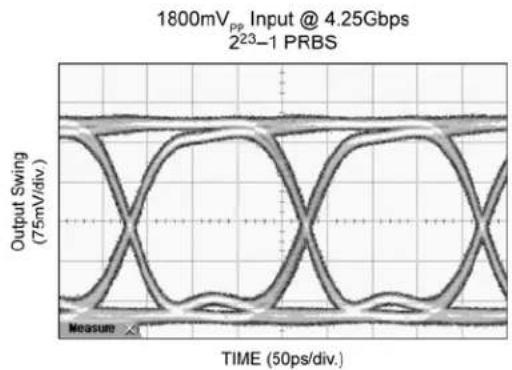
line
| Time (50ps/div.) | Output Swing (75mV/div) | | ---------------- | ------------------------ | | 0 | 0 | | 50 | 0 | | 100 | 0 | | 150 | 0 | | 200 | 0 | | 250 | 0 | | 300 | 0 | | 350 | 0 | | 400 | 0 | | 450 | 0 | | 500 | 0 | | 550 | 0 | | 600 | 0 | | 650 | 0 | | 700 | 0 | | 750 | 0 | | 800 | 0 | | 850 | 0 | | 900 | 0 | | 950 | 0 | | 1000 | 0 | | 1050 | 0 | | 1100 | 0 | | 1150 | 0 | | 1200 | 0 | | 1250 | 0 | | 1300 | 0 | | 1350 | 0 | | 1400 | 0 | | 1450 | 0 | | 1500 | 0 | | 1550 | 0 | | 1600 | 0 | | 1650 | 0 | | 1700 | 0 | | 1750 | 0 | | 1800 | 0 | | 1850 | 0 | | 1900 | 0 | | 1950 | 0 | | 2000 | 0 | | 2050 | 0 | | 2100 | 0 | | 2150 | 0 | | 2200 | 0 | | 2250 | 0 | | 2300 | 0 | | 2350 | 0 | | 2400 | 0 | | 2450 | 0 | | 2500 | 0 | | 2550 | 0 | | 2600 | 0 | | 2650 | 0 | | 2700 | 0 | | 2750 | 0 | | 2800 | 0 | | 2850 | 0 | | 2900 | 0 | | 2950 | 0 | | 3000 | 0 | | 3050 | 0 | | 3100 | 0 | | 3150 | 0 | | 3200 | 0 | | 3250 | 0 | | 3300 | 0 | | 3350 | 0 | | 3400 | 0 | | 3450 | 0 | | 3500 | 0 | | 3550 | 0 | | 3600 | 0 | | 3650 | 0 | | 3700 | 0 | | 3750 | 0 | | 3800 | 0 | | 3850 | 0 | | 3900 | 0 | | 3950 | 0 | | 4000 | 0 | | 4050 | 0 | | 4100 | 0 | | 4150 | 0 | | 4200 | 0 | | 4250 | 0 | | 4300 | 0 | | 4350 | 0 | | 4400 | 0 | | 4450 | 0 | | 4500 | 0 | | 4550 | 0 | | 4600 | 0 | | 4650 | 0 | | 4700 | 0 | | 4750 | 0 | | 4800 | 0 | | 4850 | 0 | | 4900 | 0 | | 4950 | 0 | | 5000 | 0 |
line
| R_LOSLVL (kΩ) | LOS De-Assert (mVpp) | LOS Assert (mVpp) | | ------------- | -------------------- | ------------------ | | 0.1 | ~90 | ~60 | | 10 | ~20 | ~15 |
line
| R_LOSLVL (kΩ) | HYSTERESIS (dB) | | ------------- | ---------------- | | 0.1 | 3.5 | | 10 | 3.6 |
line
| TEMPERATURE (°C) | CURRENT (mA) | | ---------------- | ------------ | | -40 | 37 | | -15 | 38 | | 10 | 39 | | 35 | 40 | | 60 | 41 | | 85 | 42 | | 110 | 43 | | 135 | 44 | | 160 | 45 |
line
| TEMPERATURE (°C) | VCO (mVpp) | | ---------------- | ---------- | | -40 | 800 | | -15 | 820 | | 0 | 830 | | 15 | 840 | | 35 | 845 | | 60 | 840 | | 85 | 830 | | 100 | 820 | | 125 | 810 | | 150 | 800 |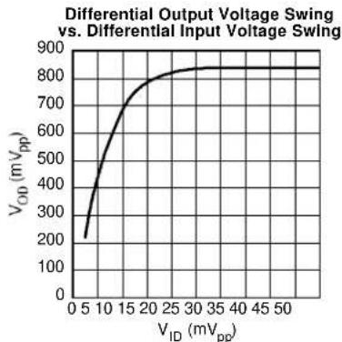
line
| V_ID (mV_pp) | V_OD (mV_pp) | | ------------ | ------------ | | 0 | 200 | | 5 | 300 | | 10 | 450 | | 15 | 650 | | 20 | 750 | | 25 | 800 | | 30 | 820 | | 35 | 830 | | 40 | 840 | | 45 | 850 | | 50 | 860 |Detailed Description
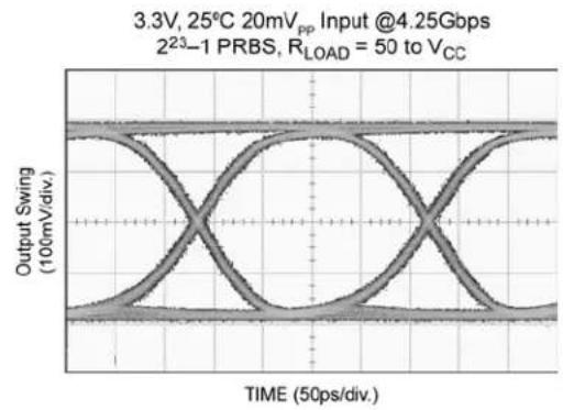
The SY88403BL low-power limiting post amplifier operates from a single +3.3V power supply, over temperatures from -40°C to +85°C. Signals with data rates up to 4.25Gbps and as small as 5mV_PP can be amplified. Figure 1 shows the allowed input voltage swing. The SY88403BL generates an LOS output, allowing feedback to /EN for output stability. LOSLVL sets the sensitivity of the input amplitude detection.
Input Amplifier/Buffer
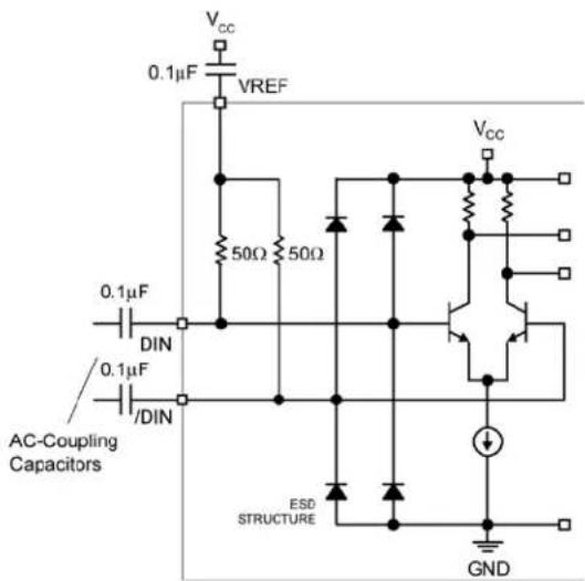
The SY88403BL's inputs are internally terminated with 50Ω to REF. If not affected by this internal termination scheme, upstream devices need to be AC-coupled to the SY88403BL's inputs. Figure 2 shows a simplified schematic of the input stage.
The high-sensitivity of the input amplifier allows signals as small as 5mV_PP to be detected and amplified. The input amplifier allows input signals as large as 1800mV_PP . Input signals are linearly amplified with a typically 38dB differential voltage gain. Since it is a limiting amplifier, the SY88403BL outputs typically 800mV_PP voltage-limited waveforms for input signals that are greater than 20mV_PP . Applications requiring the SY88403BL to operate with high-gain should have the upstream TIA placed as close as possible to the SY88403BL's input pins to ensure the best performance of the device.
Output Buffer
The SY88403BL's CML output buffer is designed to drive 50Ω lines. The output buffer requires appropriate termination for proper operation. An external 50Ω resistor to V_cc or equivalent for each output pin provides this. Figure 3 shows a simplified schematic of the output stage and includes an appropriate termination method. Of course, driving a downstream device with a CML input that is internally terminated with 50Ω to V_cc eliminates the need for external termination. As noted in the previous section, the amplifier outputs typically 800mV _PP waveforms across 25Ω total loads. The output buffer thus switches typically 16mA tail-current. Figure 4 shows the power supply current measurement, which excludes the 16mA tail-current.
Loss-of-Signal
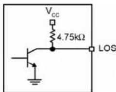
The SY88403BL incorporates a chatter-free loss-of-signal (LOS) open-collector TTL output with internal 4.75kΩ pull-up resistor as shown in Figure 5. LOS is used to determine that the input amplitude is too small to be considered a valid input. LOS asserts high if the input amplitude falls below the threshold set by LOSLVL and de-asserts low otherwise. LOS can be fed back to the enable (/EN) input to maintain output stability under a loss of signal condition. /EN de-asserts low the true output signal without removing the input signals. Typically 3.5dB LOS hysteresis is provided to prevent chattering.
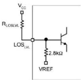
Loss-of-Signal Level Set
A programmable loss-of-signal level set pin (LOSLVL) sets the threshold of the input amplitude detection. Connecting an external resistor between V_CC and LOSLVL sets the voltage at LOSLVL. This voltage ranges from V_CC to V_REF . The external resistor creates a voltage divider between V_CC and VREF as shown in Figure 6. If desired, an appropriate external voltage may be applied rather than using a resistor. The relationship between V_LOSLVL and R_LOSLVL is given by:
$$ V = _ {C C L O S L V L} \left(1. 3 V \frac {R _ {L O S L V L}}{L O S L V L + 2 . 8 R}\right) $$
where voltages are in volts and resistances are in kΩ.
The smaller the external resistor, implying a smaller voltage difference from LOSLVL to VCC, lowers the LOS sensitivity. Hence, larger input amplitude is required to de-assert LOS. "Typical Operating Characteristics" contains graphs showing the relationship between the input amplitude detection sensitivity and R_LOSLVL .
Hysteresis
The SY88403BL provides typically 3.5dB LOS electrical hysteresis. By definition, a power ratio measured in dB is 10log (power ratio). Power is calculated as V_IN^2/R for an electrical signal. Hence the same ratio can be stated as 20log (voltage ratio). While in linear mode, the electrical voltage input changes linearly with the optical power and hence the ratios change linearly. Therefore, the optical hysteresis in dB is half the electrical hysteresis in dB given in the datasheet. The SY88403BL provides typically 1.75dB LOS optical hysteresis. As the SY88403BL is an electrical device, this datasheet refers to hysteresis in electrical terms. With 3.5dB LOS hysteresis, a voltage factor of 1.5 is required to de-assert LOS.

other
| Signal | Value | |--------|--------------| | DATA+ | 10mV (Min.) | | DATA- | 900mV (Max.) | | (DATA+) - DATA-) | 20mVpp (Min.) | | (DATA+) - DATA-) | 1800mVpp (Max.) |Figure 1. V_IS and V_ID Definition
text_image
VCC 0.1μF VREF 50Ω 50Ω 0.1μF DIN 0.1μF /DIN AC-Coupling Capacitors ESD STRUCTURE VCC GNDFigure 2. Input Structure

text_image
VCC 50Ω 50Ω DOUT Z0 = 50Ω 0.1μF /DOUT Z0 = 50Ω AC-Coupling Capacitors 16mA ESD STRUCTURE GND VCCFigure 3. Output Structure

text_image
VCC Icc 16mA 50Ω 50Ω ESD STRUCTURE 16mA GNDFigure 4. Power Supply Current Measurement
text_image
Vcc 4.75kΩ LOSFigure 5. LOS Output Structure
text_image
VCC RLOSLVL LOS LVL 2.8kΩ VREFFigure 6. LOSLVL Setting Circuit
Related Product and Support Documentation
| Part Number | Function | Data Sheet Link |
| Application Notes | Notes on Sensitivity and Hysteresis in Micrel Post Amplifier | www.micrel.com/product-info/app_hints+notes.shtml |
Package Information
text_image
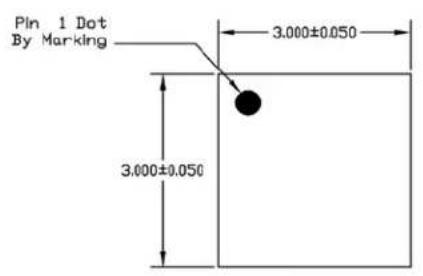
Pin 1 Dot By Marking 3.000±0.050 3.000±0.050TOP VIEW

text_image
PIN #1 IDENTIFICATION CHAMFER 0.300 X 45° 1.550±0.050 Exp. DAP 0.400±0.050 1.550±0.050 Exp. DAP 0.500 Bsc 0.230±0.050 0.400±0.050 1.500 Ref.BOTTOM VIEW
text_image
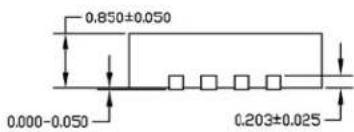
0.850±0.050 0.000-0.050 0.203±0.025SIDE VIEW
NOTE:
- ALL DIMENSIONS ARE IN MILLIMETERS.
- MAX. PACKAGE WARPAGE IS 0.05 mm.
- MAXIMUM ALLOWABE BURRS IS 0.076 mm IN ALL DIRECTIONS.
- PIN #1 ID ON TOP WILL BE LASER/INK MARKED.
16-Pin QFN
text_image
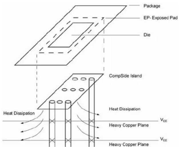
Package EP- Exposed Pad Die CompSide Island Heat Dissipation Heat Dissipation Heavy Copper Plane V_EE V_EE Heavy Copper PlanePCB Thermal Consideration for 16-Pin QFN Package
(Always solder, or equivalent, the exposed pad to the PCB)
Package Notes:
- Package meets Level 2 qualification.
- All parts are dry-packaged before shipment.
- Exposed pads must be soldered to a ground for proper thermal management.
NOTES:
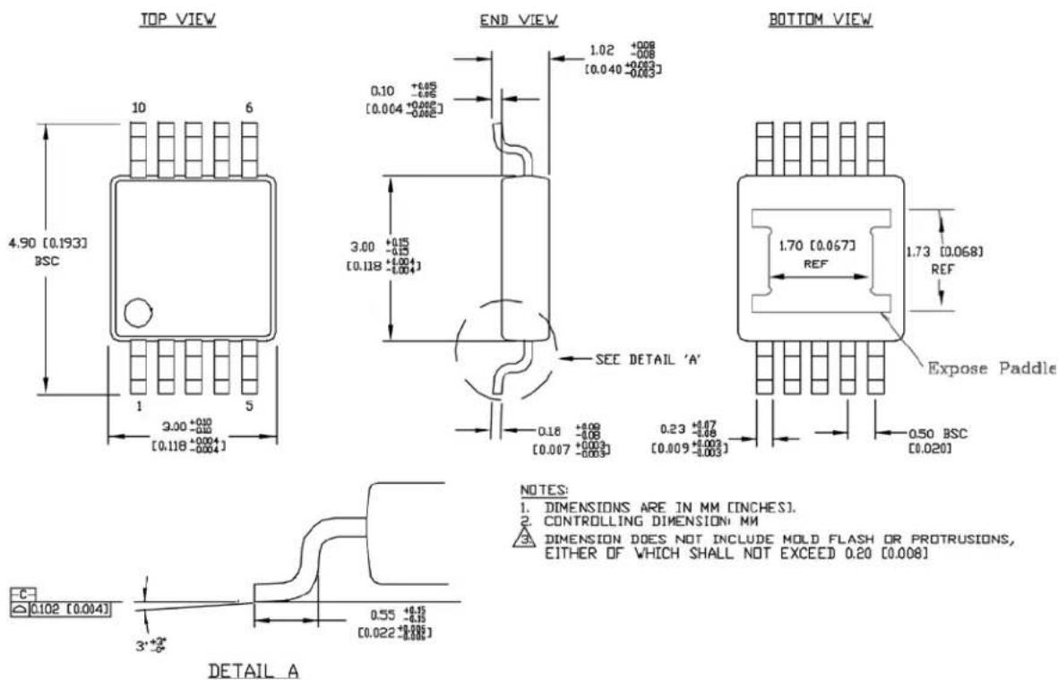
1. DIMENSIONS ARE IN MM (INCHES).
2. CONTROLLING DIMENSION: MM
3. DIMENSION DOES NOT INCLUDE MOLD FLASH OR PROTRUSIONS,
EITHER OF WHICH SHALL NOT EXCEED 0.20 [0.008]
10-Pin EPAD-MSOP (K10-2)
MICREL, INC. 2180 FORTUNE DRIVE SAN JOSE, CA 95131 USA
TEL +1 (408) 944-0800 FAX +1 (408) 474-1000 WEB http://www.micrel.com
The information furnished by Micrel in this data sheet is believed to be accurate and reliable. However, no responsibility is assumed by Micrel for its use. Micrel reserves the right to change circuitry and specifications at any time without notification to the customer.
Micrel Products are not designed or authorized for use as components in life support appliances, devices or systems where malfunction of a product can reasonably be expected to result in personal injury. Life support devices or systems are devices or systems that (a) are intended for surgical implant into the body or (b) support or sustain life, and whose failure to perform can be reasonably expected to result in a significant injury to the user. A Purchaser's use or sale of Micrel Products for use in life support appliances, devices or systems is a Purchaser's own risk and Purchaser agrees to fully indemnify Micrel for any damages resulting from such use or sale.
© 2005 Micrel, Incorporated.