PCI-1713U-BE - PCI card Advantech - Free user manual and instructions
Find the device manual for free PCI-1713U-BE Advantech in PDF.

| Product Type | PCI Data Acquisition Card |
| Brand | Advantech |
| Model | PCI-1713U-BE |
| Dimensions (approx.) | 175 mm x 100 mm (standard PCI card) |
| Weight (approx.) | 100 g |
| Power Supply | +5 V DC from PCI slot (typical 500 mA) |
| Analog Input Channels | 16 single-ended / 8 differential |
| Resolution | 16-bit |
| Sampling Rate | 100 kS/s (max) |
| Input Range | ±10 V, ±5 V, ±2.5 V, ±1.25 V, ±0.625 V (programmable) |
| Digital I/O | 16 TTL-compatible digital I/O lines |
| Bus Interface | PCI 2.2 |
| Operating Temperature | 0°C to 60°C |
| Storage Temperature | -20°C to 70°C |
| Humidity | 5% to 95% RH, non-condensing |
| Connector | 68-pin SCSI-II female connector |
| Software Support | Windows, Linux drivers; Advantech DAQNavi SDK |
| Maintenance | Keep free of dust; avoid electrostatic discharge |
| Safety | Install in grounded computer chassis |
| Spare Parts / Repairability | Not user-serviceable; contact Advantech support |
Frequently Asked Questions - PCI-1713U-BE Advantech
User questions about PCI-1713U-BE Advantech
0 question about this device. Answer the ones you know or ask your own.
Ask a new question about this device
Download the instructions for your PCI card in PDF format for free! Find your manual PCI-1713U-BE - Advantech and take your electronic device back in hand. On this page are published all the documents necessary for the use of your device. PCI-1713U-BE by Advantech.
USER MANUAL PCI-1713U-BE Advantech
The documentation and the software included with this product are copyrighted 2009 by Advantech Co., Ltd. All rights are reserved. Advantech Co., Ltd. reserves the right to make improvements in the products described in this manual at any time without notice. No part of this manual may be reproduced, copied, translated or transmitted in any form or by any means without the prior written permission of Advantech Co., Ltd. Information provided in this manual is intended to be accurate and reliable. However, Advantech Co., Ltd. assumes no responsibility for its use, nor for any infringements of the rights of third parties, which may result from its use.
Acknowledgements
Intel and Pentium are trademarks of Intel Corporation.
Microsoft Windows and MS-DOS are registered trademarks of
Microsoft Corp.
All other product names or trademarks are properties of their respective owners.
Part No. 20031713U01 1st Edition
Printed in Taiwan October 2009
Product Warranty (2 years)
Advantech warrants to you, the original purchaser, that each of its products will be free from defects in materials and workmanship for two years from the date of purchase.
This warranty does not apply to any products which have been repaired or altered by persons other than repair personnel authorized by Advantech, or which have been subject to misuse, abuse, accident or improper installation. Advantech assumes no liability under the terms of this warranty as a consequence of such events.
Because of Advantech's high quality-control standards and rigorous testing, most of our customers never need to use our repair service. If an Advantech product is defective, it will be repaired or replaced at no charge during the warranty period. For out-of-warranty repairs, you will be billed according to the cost of replacement materials, service time and freight. Please consult your dealer for more details.
If you think you have a defective product, follow these steps:
- Collect all the information about the problem encountered. (For example, CPU speed, Advantech products used, other hardware and software used, etc.) Note anything abnormal and list any onscreen messages you get when the problem occurs.
- Call your dealer and describe the problem. Please have your manual, product, and any helpful information readily available.
- If your product is diagnosed as defective, obtain an RMA (return merchandise authorization) number from your dealer. This allows us to process your return more quickly.
- Carefully pack the defective product, a fully-completed Repair and Replacement Order Card and a photocopy proof of purchase date (such as your sales receipt) in a shippable container. A product returned without proof of the purchase date is not eligible for warranty service.
- Write the RMA number visibly on the outside of the package and ship it prepaid to your dealer.
Declaration of Conformity
CE
This product has passed the CE test for environmental specifications when shielded cables are used for external wiring. We recommend the use of shielded cables. This kind of cable is available from Advantech. Please contact your local supplier for ordering information.
Technical Support and Assistance
Step 1. Visit the Advantech web site at www.advantech.com/support where you can find the latest information about the product.
Step 2. Contact your distributor, sales representative, or Advantech's customer service center for technical support if you need additional assistance. Please have the following information ready before you call:
- Product name and serial number
- Description of your peripheral attachments
- Description of your software (operating system, version, application software, etc.)
- A complete description of the problem
- The exact wording of any error messages
Safety Instructions
- Read these safety instructions carefully.
- Keep this User's Manual for later reference.
- Disconnect this equipment from any AC outlet before cleaning. Use a damp cloth. Do not use liquid or spray detergents for cleaning.
-
For plug-in equipment, the power outlet socket must be located near the equipment and must be easily accessible.
-
Keep this equipment away from humidity.
-
Put this equipment on a reliable surface during installation. Dropping it or letting it fall may cause damage.
-
The openings on the enclosure are for air convection. Protect the equipment from overheating. DO NOT COVER THE OPENINGS.
-
Make sure the voltage of the power source is correct before connecting the equipment to the power outlet.
-
Position the power cord so that people cannot step on it. Do not place anything over the power cord.
-
All cautions and warnings on the equipment should be noted.
-
If the equipment is not used for a long time, disconnect it from the power source to avoid damage by transient overvoltage.
-
Never pour any liquid into an opening. This may cause fire or electrical shock.
-
Never open the equipment. For safety reasons, the equipment should be opened only by qualified service personnel.
-
If one of the following situations arises, get the equipment checked by service personnel:
a. The power cord or plug is damaged.
b. Liquid has penetrated into the equipment.
c. The equipment has been exposed to moisture.
d. The equipment does not work well, or you cannot get it to work according to the user's manual.
e. The equipment has been dropped and damaged.
f. The equipment has obvious signs of breakage.
- DO NOT LEAVE THIS EQUIPMENT IN AN ENVIRONMENT WHERE THE STORAGE TEMPERATURE MAY GO BELOW -
20°C (-4°F) OR ABOVE 60°C (140°F). THIS COULD DAMAGE THE EQUIPMENT. THE EQUIPMENT SHOULD BE IN A CONTROLLED ENVIRONMENT.
- CAUTION: DANGER OF EXPLOSION IF BATTERY IS INCORRECTLY REPLACED. REPLACE ONLY WITH THE SAME OR EQUIVALENT TYPE RECOMMENDED BY THE MANUFACTURER, DISCARD USED BATTERIES ACCORDING TO THE MANUFACTURER'S INSTRUCTIONS.
The sound pressure level at the operator's position according to IEC 704-1:1982 is no more than 70 dB (A).
DISCLAIMER: This set of instructions is given according to IEC 704-1. Advantech disclaims all responsibility for the accuracy of any statements contained herein.
Contents
Chapter 1 Overview ...... 2
1.1 Introduction....2
1.2 Features .... 3
1.3 Specifications 3
1.4 Block Diagram 5
Chapter 2 Installation ....8
2.1 Initial Inspection.... 8
2.2 Unpacking 8
2.3 Installation Instructions....9
Chapter 3 Signal Connections .... 12
3.1 Overview 12
3.2 I/O Connector.... 12
Figure 3.1:I/O Connector Pin Assignments ..... 13
3.3 Analog Input Connections.... 14
Figure 3.2: Single-ended Input Ch. 14
Figure 3.3:Differential Input Ch. - Grounded ..... 15
Figure 3.4:Differential Input Ch. - Floating ..... 16
3.4 Field Wiring Considerations 17
Chapter 4 Calibration ...... 20
4.1 Introduction 20
4.2 VR Assignments.... 20
Figure 4.1:PCL-1713U VR Assignments ....20
4.3 Board ID Settings.... 21
Figure 4.2:Board ID Switch 21
Table 4.1:Board ID Settings 21
4.4 A/D Calibration.... 22
Appendix A Specifications 28
A.1 General 28
A.2 Analog Input.... 29
Overview
Sections include:
- Introduction
- Features
- Specifications
- Block Diagram
Chapter 1 Overview
1.1 Introduction
The PCI-1713U is a 12-bit 32-channel analog input card for the PCI bus. It provides 32 analog input channels with a sampling rate up to 100k samples/s, 12-bit resolution and isolation protection of 2500 VDC.
PCI-bus Plug and Play
The PCI-1713U uses a PCI controller to interface the card with the PCI bus. The controller fully implements the PCI bus specification Rev 2.1. All bus relative configurations, such as base address and interrupt assignment, are automatically controlled by software.
Flexible Input Types and Range Settings
The PCI-1713U features an automatic channel/gain scanning circuit. The circuit, rather than your software, controls multiplexer switching during sampling. The on-board SRAM stores different gain values and configurations for each channel. This design lets you perform multi-channel sampling with different gains for each channel and with free combination of single-ended and differential inputs.
High-speed Data Acquisition
The PCI-1713U provides a sampling rate up to 100k samples/s. It has an on-board FIFO buffer, which can store up to 4K A/D samples and generates an interrupt signal when the FIFO is half full. This feature provides continuous high-speed data transfer and more predictable performance on Windows systems.
Supports Software, Internal and External Pacer Triggering
The PCI-1713U supports three kinds of trigger modes for A/D conversion: software triggering, internal pacer triggering and external pacer triggering. The software trigger allows users to acquire a sample when it is needed; the internal pacer triggers continuous high-speed data acquisition. The PCI-1713U also accepts external trigger sources, allowing synchronous sampling with external devices.
Satisfies the Need for Isolation Protection
The PCI-1713U provides 2500VDC optical isolation protection between the inputs and the PC bus to protect the PC and peripherals from damage due to high voltages on the input lines. It is ideal for the situations where budget-conscious users require flexibility, stability and a high level of isolation protection for their data acquisition system.
1.2 Features
• 32 single-ended or 16 differential analog inputs, or a combination
• 12-bit A/D converter, with up to 100 kHz sampling rate
- Programmable gain for each input channel
• Automatic channel/gain scanning
- Onboard 4k samples FIFO buffer
- Programmable pacer
1.3 Specifications
Analog Input:
- Channels: 32 single-ended or 16 differential (software programmable)
- Resolution: 12-bit
- Onboard FIFO: 4k samples
- Conversion time: 2.5 s
Input Range:
- Bipolar: ± 10V,± 5V,± 2.5V,± 1.25V,± 0.625V
- Unipolar: 0 10 ~V, 0 5 ~V, 0 2.5 ~V, 0 1.25 ~V
• Maximum Input Overvoltage: ±30 V
• Isolation Protection: 2,500V
• Maximum sampling rate: 100 kHz
• Accuracy: (depending on gain)
Gain Accuracy
0.5, 1 0.1% of FSR±1LSB
2 0.2% of FSR±1LSB
4 0.2% of FSR±1LSB
8 0.4% of FSR±1LSB
• Linearity error: ±1 LSB
- Drift: Typical 30 PPM / °C (0 \~ 60 °C)
- Input impedance: 1 GΩ
- Sampling mode: Software, on-board programmable pacer or external
- Trigger voltage: Low: 0\~2 V; High: 2.8\~5 V
Programmable Timer/Counter
• Counter chip: 82C54 or equivalent
- Counters: 3 channels, 16 bits
2 channels are permanently configured as programmable pacers; 1 channel is un-used.
- Time base:
Channel 1: 10 MHz
Channel 2: Takes input from output of channel 1
Channel 0: unused.
General:
• I/O Connector: 37-pin D-type female connector
- Dimensions: 175 mm x 100 mm (6.9" x 3.9")
• Power consumption:+5 V @ 850 mA (Typical),
• +5 V @ 1.0 A (Max.)
- Operating temperature: 0 +60^ C (32 \~ 140 °F)
- Storage temperature: -20 +70^ C (-4 \~ 158 °F)
- Operating humidity: 5 95% RH non-condensing
- MTBF: over 85,310 hrs @ 25 °C, grounded, fixed environment

flowchart
graph TD
    A["PCI Bus"] --> B["PCI Target Controller"]
    B --> C["Address Decoder"]
    B --> D["INT Generator"]
    D --> E["4K FIFO"]
    E --> F["ADC Control Logic"]
    F --> G["Gain Code Generator"]
    F --> H["Channel Code Generator"]
    G --> I["12 bit A/D Converter"]
    H --> J["Multiplexer 32 S.E. or 16 Diff"]
    I --> K["PGIA"]
    J --> L["PGIA + -"]
    K --> M["Isolation"]
    L --> N["Isolation"]
    M --> O["EXT_TRG"]
    N --> P["10 MHz OSC"]
    O --> Q["Data Bus"]
    P --> Q
    Q --> R["Counter 1"]
    Q --> S["Counter 2"]
    R --> T["Pacer"]
    S --> T
    T --> U["Address Bus"]
    U --> V["PCI Bus"]
    V --> W["PCI Target Controller"]
    W --> X["Address Decoder"]
    X --> Y["10 MHz OSC"]
    Y --> Z["Pacer"]
    Z --> AA["Data Bus"]
    AA --> AB["4K FIFO"]
    AB --> AC["ADC Control Logic"]
    AC --> AD["Gain Code Generator"]
    AC --> AE["Channel Code Generator"]
    AD --> AF["Isolation"]
    AE --> AG["Isolation"]
    AF --> AH["12 bit A/D Converter"]
    AG --> AI["Multiplexer 32 S.E. or 16 Diff"]
    AH --> AJ["PGIA + -"]
    AI --> AK["AI 0, AI 1, ..., AI31"]
Installation
Sections include:
- Initial Inspection
- Unpacking
• Installation Instructions
Chapter 2 Installation
2.1 Initial Inspection
Before installing the PCI-1713U, check the card for visible damage. We have carefully inspected the card both mechanically and electrically before shipment. It should be free of marks and in perfect order upon receipt.
As you unpack the PCI-1713U, check it for signs of shipping damage (damaged box, scratches, dents, etc.). If it is damaged or fails to meet specifications, notify our service department or your local sales representative immediately. Also, call the carrier immediately and retain the shipping carton and packing materials for inspection by the carrier. We will then make arrangements to repair or replace the unit.
2.2 Unpacking
The PCI-1713U contains components that are sensitive and vulnerable to static electricity. Discharge any static electricity on your body to ground by touching the back of the system unit (grounded metal) before you touch the board.
Remove the PCI-1713U card from its protective packaging by grasping the card's rear panel. Handle the card only by its edges to avoid static discharge which could damage its integrated circuits. Keep the antistatic package. Whenever you remove the card from the PC, protect the card by storing it in this package.
You should also avoid contact with materials that hold static electricity such as plastic, vinyl and styrofoam.
Check the product contents inside the packing. There should be one card, one CD-ROM, and this manual. Make sure nothing is missing.
The PCI-1713U can be installed in any PCI slot in the computer. However, refer to the computer user's manual to avoid any mistakes and danger before you follow the installation procedure below:
- Turn off your computer and any accessories connected to the computer. Warning! TURN OFF your computer power supply whenever you install or remove any card, or connect and disconnect cables.
- Disconnect the power cord /other cables from the back of the computer.
- Remove the cover of the computer.
- Select an empty +5 V PCI slot. Remove the screw that secures the expansion slot cover to the system unit. Save the screw to secure the interface card retaining bracket.
- Carefully grasp the upper edge of the PCI-1713U. Align the hole in the retaining bracket with the hole on the expansion slot and align the gold striped edge connector with the expansion slot socket. Press the card into the socket gently but firmly. Make sure the card fits the slot tightly.
- Secure the PCI-1713U by screwing the mounting bracket to the back panel of the computer.
- Attach any accessories (D-type cable, terminal board, etc.) to the card.
- Replace the cover of your computer. Reconnect any cables.
- Turn the computer power on.
Signal Connections
Sections include:
- Overview
- I/O Connector
• Analog Input Connections
• Field Wiring Considerations
Chapter 3 Signal Connections
3.1 Overview
Correct signal connections are one of the most important factors in ensuring that your application system is sending and receiving data correctly. A good signal connection can avoid much unnecessary and costly damage to your valuable PC and other hardware devices. This chapter will provide some useful information about how to connect analog input signals to the PCI-1713U card via the I/O connector.
3.2 I/O Connector
The I/O connector for the PCI-1713U card is a 37-pin D-type connector which you can connect to 37-pin D-type accessories with Advantech's PCL-10137 cable.
Note!: The PCI-1713U does not include the PCL-10137 cable assembly.
The following figure shows the pin assignments for the 37-pin I/O connector on the PCI-1713U card.
| AI0 | 1 | 20 | AI1 |
| AI2 | 2 | 21 | AI3 |
| AI4 | 3 | 22 | AI5 |
| AI6 | 4 | 23 | AI7 |
| AI8 | 5 | 24 | AI9 |
| AI10 | 6 | 25 | AI11 |
| AI12 | 7 | 26 | AI13 |
| AI14 | 8 | 27 | AI15 |
| GND | 9 | 28 | GND |
| GND | 10 | 29 | GND |
| AI16 | 11 | 30 | AI17 |
| AI18 | 12 | 31 | AI19 |
| AI20 | 13 | 32 | AI21 |
| AI22 | 14 | 33 | AI23 |
| AI24 | 15 | 34 | AI25 |
| AI26 | 16 | 35 | AI27 |
| AI28 | 17 | 36 | AI29 |
| AI30 | 18 | 37 | AI31 |
| EXT_TRG | 19 |
Figure 3.1: I/O Connector Pin Assignments
This section continues to describe how to make analog input signal connections to the PCI-1713U card via the I/O connector.
Single-ended Channel Connections
The single-ended input configuration has only one signal wire for each channel, and the measured voltage (Vm) is the voltage of the wire referred to the common ground.
A signal source without a local ground is also called a “floating source”. It is fairly simple to connect a single-ended channel to a floating signal source. In this mode, the PCI-1713U card provides a reference ground for external floating signal sources.

flowchart
graph TD
    A["Measured Voltage"] --> B["PGIA"]
    B --> C["Multiplexers"]
    C --> D["I/O Connector"]
    D --> E["Floating Signal Source"]
    E --> F["ExternalInternal"]
    G["Vm"] --> B
    H["+"] --> B
    I["-"] --> B
    J["A10"] --> C
    K["A11"] --> C
    L["A131"] --> C
    M["GND"] --> D
Figure 3.2: Single-ended Input Ch.
Differential Channel Connections
The differential input configuration has two signal wires for each channel, and the differential input responds only to voltage differences between High and Low inputs. On the PCI-1713U card, when all channels are configured to differential input, up to 16 analog channels are available.
flowchart
graph TD
    A["PGIA"] -->|Measured Voltage Vm| B["+"]
    A -->|-| C["-"]
    B --> D["Multiplexer"]
    C --> E["Multiplexer"]
    D --> F["AI0"]
    D --> G["AI2"]
    D --> H["AI30"]
    E --> I["AI1"]
    E --> J["AI3"]
    E --> K["AI31"]
    F --> L["ExternalInternal"]
    G --> L
    H --> L
    I --> L
    J --> L
    K --> L
    L --> M["Ground-Referenced Signal Source"]
    L --> N["Vcm"]
    L --> O["GND"]
    O --> P["I/O Connector"]
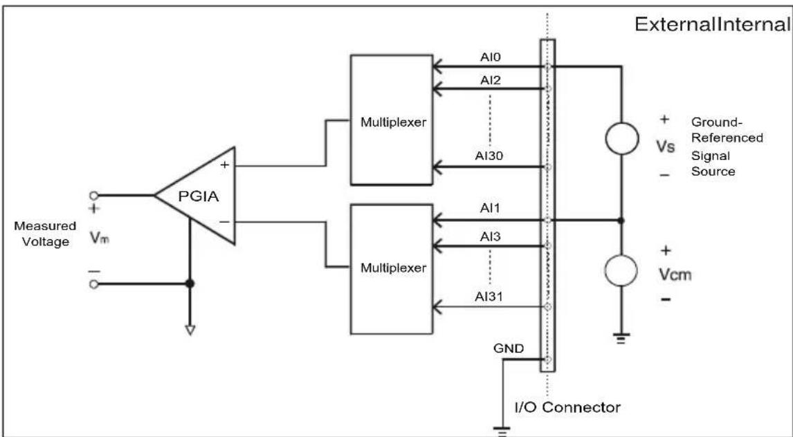
Figure 3.3: Differential Input Ch. - Grounded
If one side of the signal source is connected to a local ground, the signal source is ground-referenced. The ground of the signal source and the ground of the PCI-1713U will not be at exactly the same voltage, as they are connected through the ground return of the equipment and building wiring. The difference between the ground voltages forms a common-mode voltage ( V_cm ).
To avoid the ground loop noise effect caused by common-mode voltages, you can connect the signal ground to the Low input. Figure 3-3 shows a differential channel connection between a ground-referenced signal source and an input channel on the PCI-1713U card. With this connection, the PGIA rejects a common-mode voltage V_cm between the signal source and the PCI-1713U ground, shown as V_cm in Figure 3-3.
flowchart
graph LR
    A["Measured Voltage Vm"] --> B["PGIA"]
    B --> C["Multiplexer"]
    B --> D["Multiplexer"]
    C --> E["Internal"]
    D --> E
    E --> F["External"]
    G["I/O Connector"] --> H["I/O Connector"]
    I["+ Vs - Floating Signal Source"] --> J["r_a"]
    J --> K["r_b"]
    K --> L["Ground"]
    M["Al0, Al2, Al30"] --> N["Internal"]
    O["Al1, Al3, Al31"] --> P["Internal"]
    Q["GND"] --> R["Internal"]
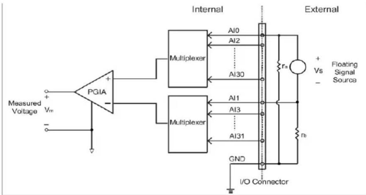
Figure 3.4: Differential Input Ch. - Floating
If a floating signal source is connected to the differential input channel, the signal source may exceed the common-mode signal range of the PGIA, and the PGIA will be saturated with erroneous voltage-readings. You must therefore reference the signal source to the AIGND.
Figure 3-4 shows a differential channel connection between a floating signal source and an input channel on the PCI-1713U card. In this figure, each side of the floating signal source is connected through a resistor to the AIGND. This connection can reject the common-mode voltage between the signal source and the PCI-1713U card ground.
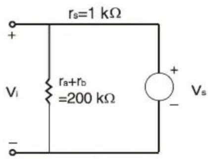
text_image
rs=1 kΩ + Vi ra+rb =200 kΩ - Vs +V_s : ideal signal source
V_i : measured signal source
r_s : output impedance of signal source
r_a , r_b : series-wound resistors
$$ V _ {i} = \frac {r _ {a} + r _ {b}}{r _ {s} + r _ {a} + r _ {b}} V _ {s} = \frac {2 0 0}{1 + 2 0 0} V _ {s} = \frac {2 0 0}{2 0 1} V _ {s} $$
$$ \text { Gain error } = \frac {\mathrm{V} _ {\mathrm{i}} - \mathrm{V} _ {\mathrm{s}}}{\mathrm{V} _ {\mathrm{s}}} = - \frac {1}{2 0 1} = - 0.5 \% $$
External Trigger Source Connection
In addition to pacer triggering, the PCI-1713U card also allows external triggering for A/D conversions. A low-to-high edge coming from EXT_TRG will trigger an A/D conversion on the PCI-1713U board.
Note: Don't connect any signal to the EXT_TRG pin when the external trigger function is not being used.
Note: If you use external triggering for A/D conversions, we recommend you choose differential mode for all analog input signals, so as to reduce the cross-talk noise caused by the external trigger source.
3.4 Field Wiring Considerations
When you use the PCI-1713U card to acquire outside data, environmental noise can seriously affect the accuracy of your measurements if you don't provide any protection. The following suggestions will be helpful when running signal wires between signal sources and the PCI-1713U card.
- Please make sure that you have carefully routed signal cables to the card. You must separate the cabling from noise sources. Try to keep video monitors far away from the analog signal cables, because these are a common noise source in a PCI data acquisition system.
- If you want to reduce common-mode noise, try to use differential analog input connections.
- If you do not want your signals to be affected when travelling through areas with high electromagnetic interference or large magnetic fields, try the following routing techniques: Use individually shielded, twisted-pair wires to connect analog input signals to the board, i.e. the signals connected to the High and Low inputs aretwisted together and covered with a shield. Finally, connect the shield only to one point at the signal source ground.
- Make sure that your signal lines do not travel through conduits, because these may contain power lines. Also, keep your signals far from electric motors, breakers or welding equipment, as these can create magnetic fields.
- Keep a reasonable distance between high-voltage (or high-current) lines and signal cables connected to the PCI-1713U card if the cables run parallel, or route signal cables at right angles to high voltage/current cables.
Calibration
Sections include:
- Introduction
- VR Assignments
- Board ID Settings
• A/D Calibration
Chapter 4 Calibration
4.1 Introduction
Regular calibration checks are important to maintain accuracy in data acquisition and control applications. To assist users in the A/D calibration process, we provide the Advantech Device Manager, on the PCI-1713U software CD-ROM.
The Advantech Device Manager makes A/D calibrations easy. It leads you through the calibration and setup procedure with a variety of prompts and graphic displays, showing you all of the correct settings and adjustments. This chapter offers a brief guide to these calibration programs.
To perform a satisfactory calibration, you need a 41/2-digit digital multi-meter and a voltage calibrator or a stable, noise free D. C. voltage source.
4.2 VR Assignments
There are four variable resistors (VRs) on the PCL-1713U card. They help you to make accurate adjustments on all A/D channels. Please refer to the following figure for VR positions.
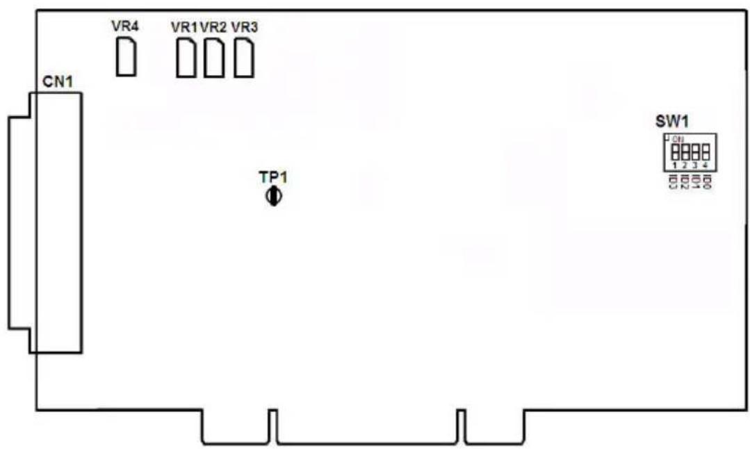
text_image
CN1 VR4 VR1VR2 VR3 TP1 SW1 1 2 3 4Figure 4.1: PCL-1713U VR Assignments
The following list shows the function of each VR:
VR Function
VR1 A/D full scale (gain)
VR2 A/D bipolar offset
VR3 A/D unipolar offset
VR4 PGIA offset
TP1 PGIA output
4.3 Board ID Settings
The PCI-1713U has a built-in DIP switch (SW1), which is used to define each card's board ID. You can determine the board ID on the register as shown in Table 4.1. When there are multiple cards on the same chassis, this board ID setting function is useful for identifying each card's device number through board ID. We set the PCI-1713U board ID as 0 at the factory. If you need to adjust it to other board ID, set the SW1 by referring to DIP switch setting.

Figure 4.2: Board ID Switch
| Table 4.1: Board ID Settings | ||||
| SW1 Position2 Position3 Position4 | ||||
| Board ID ID3 ID2 ID1 | ID0 | |||
| 15 | OFF | OFF | OFF | OFF |
| 14 | OFF | OFF | OFF | ON |
| 13 | OFF | OFF | ON | OFF |
| : | : | : | : | : |
| 1 | ON | ON | ON | OFF |
| 0* | ON | ON | ON ON | |
* Default setting is 0
- Connect Pin1 to Pin9 and measure the output as "V1" from TP1. (PCI-1713 only, not available for PCI-1713U)

text_image
A/D Calibration Wizard Analog Input Voltage Decimal VR 4 1 2 3 TP1 O PCI-1713 Step 1: PGIA_OFFSET1 Connect the AI0(Pin1) to the ground(Pin9). Please measure TP1 output as 'V1' with a 4 1/2-digit digital multimeter. Note: Not available for PCI-1713U, skip it- Adjust VR4 until | V1 - V2 | < 0.05mV. For example, if the V1 is 0.1mV in the beginning and you get V2 as 0.02mV after adjusting the VR4, you have to adjust the VR4 again. (PCI-1713 only, not available for PCI-1713U)
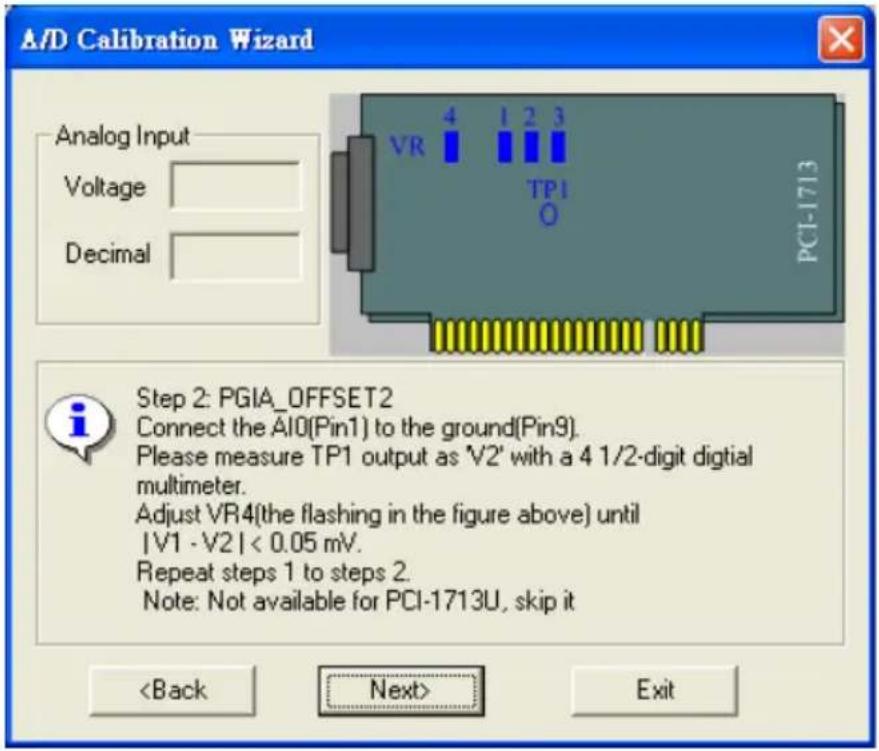
text_image
A/D Calibration Wizard Analog Input Voltage Decimal VR 4 1 2 3 TP1 O PCI-1713 Step 2: PGIA_OFFSET2 Connect the AI0(Pin1) to the ground(Pin9). Please measure TP1 output as 'V2' with a 4 1/2-digit digital multimeter. Adjust VR4(the flashing in the figure above) until |V1 - V2 | < 0.05 mV. Repeat steps 1 to steps 2. Note: Not available for PCI-1713U, skip it- Input -5V to AI0 by signal generator and check if the "Decimal" flickers between 0 and 1. For example, it is 3 for my calibration, so I have to adjust the VR2.
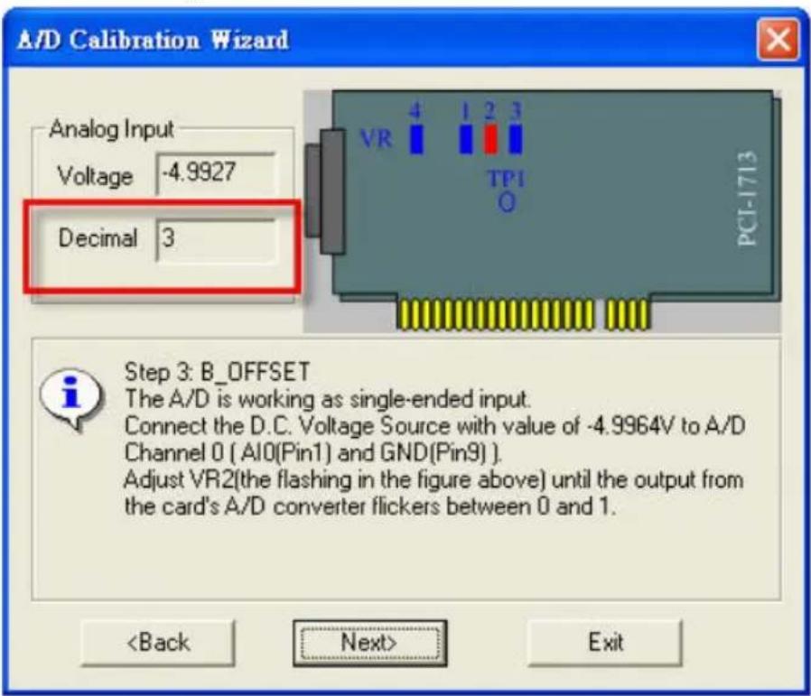
text_image
A/D Calibration Wizard Analog Input Voltage -4.9927 Decimal 3 Step 3: B_OFFSET The A/D is working as single-ended input. Connect the D.C. Voltage Source with value of -4.9964V to A/D Channel 0 ( AI0(Pin1) and GND(Pin9) ) . Adjust VR2(the flashing in the figure above) until the output from the card's A/D converter flickers between 0 and 1.- Input 5V to AI0 by signal generator and check if the "Decimal" flickers between 4094 and 4095.

text_image
A/D Calibration Wizard Analog Input Voltage 4.9976 Decimal 4095 Step 4: AD_FS The A/D is working as single-ended input. Connect the D.C. Voltage Source with value of 4.9988V to A/D Channel 0 ( AI0(Pin1) and GND(Pin9) ) . Adjust VR1(the flashing in the figure above) until the output from the card's A/D converter flickers between 4094 and 4095. Repeat steps 3 to steps 4.- Input 5V to AI1 by signal generator and check if the "Decimal" flickers between 2047 and 2048.
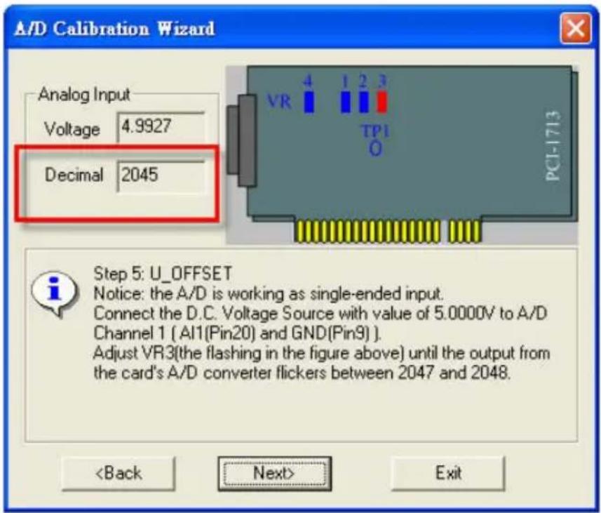
text_image
A/D Calibration Wizard Analog Input Voltage 4.9927 Decimal 2045 Step 5: U_OFFSET Notice: the A/D is working as single-ended input. Connect the D.C. Voltage Source with value of 5.0000V to A/D Channel 1 (AI1(Pin20) and GND(Pin9)). Adjust VR3(the flashing in the figure above) until the output from the card's A/D converter flickers between 2047 and 2048.Calibration finished.
1713U
| A/D code Mapping Voltage | |||
| Hex. Dec. Bipolar ±5V | Unipolar 0 to 10V | ||
| 000h 0 | -4.9971V 0V | ||
| 7FFh 20 | 47 -0.0024V | 4.9947V | |
| 800h 20 | 48 0V 4.9971V | ||
| FFFh 40 | 95 +4.9947V | 9.9918V | |
APPENDIX

text_image
ASpecifications
Appendix A Specifications
A.1 General
| I/O Connector Type 37- | pin D-type female connector | |
| Dimensions 175 x 100 mm (6.9" x 3.9") | ||
| Power Consumption Typical +5 V @850 mA | ||
| Max. +5 V @1 A | ||
| Temperature Operation 0~60°C (32~140°F) | ||
| Storage -20~70°C (-4~158°F) | ||
| Relative Humidity 5~95%RH non-condensing (refer to IEC 68-2-3) | ||
| Certification CE certified | ||
A.2 Analog Input
| Channels 32 | single-ended or 16 differential or combination | ||||||||
| Resolution 12 | -bit | ||||||||
| FIFO Size 4k | samples | ||||||||
| Max. Sampling Rate | 100 kS/s | ||||||||
| Isolation Protection | 2,500 V | ||||||||
| Conversion Time | 2.5 μs | ||||||||
| Input Range and Gain List | Gain 0.5 1 2 4 8 | ||||||||
| Unipolar N/A 0~10 0~5 0~2.5 0~1.25 | |||||||||
| Bipolar | ±10 | ±5 | ±2.5 | ±1.25 | ±0.625 | ||||
| Drift 30 ppm/° | C (0~60°C) | ||||||||
| Small Signal BW for PGA | 170 kHz | ||||||||
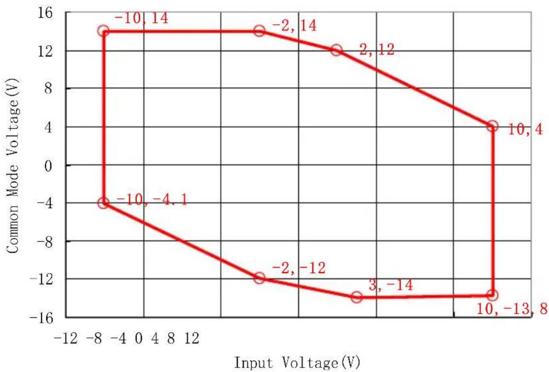
| Max. Input Voltage* | Common Mode Voltage(V) | -11 | -8 | -6 | -4~4 | 6 | 8 | 11 | |
| Max. Input Voltage(V) | -3~10 | -6~10 | -8~10 | -10~10 | -10~8 | -10~6 | -10~3 | ||
| Input Impedance | 1 GΩ | ||||||||
| Trigger Mode | Software, on-board programmable pacer or external | ||||||||
| Accuracy | DC | INLE: ±3 LSB | |||||||
| DNLE: ±1 LSB | |||||||||
| Monotonicity: 12 bits | |||||||||
| Offset error: Adjustable to zero | |||||||||
| Gain | 0.5 | 1 | 2 | 4 | 8 | ||||
| Gain Error (% FSR) | 0.1 | 0.1 | 0.2 | 0.2 | 0.4 | ||||
| AC | SNR: 68dB | ||||||||
| ENOB: 10.5 bits | |||||||||
| External TTL Trigger Input | Low | 2.0 V max. | |||||||
| High | 2.8 V min. | ||||||||
*Note: The maximum input voltage may vary according to the common mode voltage as shown below: