PCIE-1604B-AE - PCI card Advantech - Free user manual and instructions
Find the device manual for free PCIE-1604B-AE Advantech in PDF.

User questions about PCIE-1604B-AE Advantech
0 question about this device. Answer the ones you know or ask your own.
Ask a new question about this device
Download the instructions for your PCI card in PDF format for free! Find your manual PCIE-1604B-AE - Advantech and take your electronic device back in hand. On this page are published all the documents necessary for the use of your device. PCIE-1604B-AE by Advantech.
USER MANUAL PCIE-1604B-AE Advantech
natural_image
Illustration of a computer motherboard with two components, one showing internal circuitry and the other a rectangular electronic device (no text or symbols)PCI Express COMM Series User Manual
Industrial Serial Communication Cards
Copyright
The documentation and the software included with this product are copyrighted 2015 by Advantech Co., Ltd. All rights are reserved. Advantech Co., Ltd. reserves the right to make improvements in the products described in this manual at any time without notice. No part of this manual may be reproduced, copied, translated or transmitted in any form or by any means without the prior written permission of Advantech Co., Ltd. Information provided in this manual is intended to be accurate and reliable. However, Advantech Co., Ltd. assumes no responsibility for its use, nor for any infringements of the rights of third parties, which may result from its use.
Acknowledgements
Intel and Pentium are trademarks of Intel Corporation.
Microsoft Windows and MS-DOS are registered trademarks of Microsoft Corp.
All other product names or trademarks are properties of their respective owners.
Product Warranty (5years)
Advantech warrants to you, the original purchaser, that each of its products will be free from defects in materials and workmanship for five years from the date of purchase.
This warranty does not apply to any products which have been repaired or altered by persons other than repair personnel authorized by Advantech, or which have been subject to misuse, abuse, accident or improper installation. Advantech assumes no liability under the terms of this warranty as a consequence of such events.
Because of Advantech's high quality-control standards and rigorous testing, most of our customers never need to use our repair service. If an Advantech product is defective, it will be repaired or replaced at no charge during the warranty period. For out-of-warranty repairs, you will be billed according to the cost of replacement materials, service time and freight. Please consult your dealer for more details.
If you think you have a defective product, follow these steps:
-
Collect all the information about the problem encountered. (For example, CPU speed, Advantech products used, other hardware and software used, etc.) Note anything abnormal and list any onscreen messages you get when the problem occurs.
-
Call your dealer and describe the problem. Please have your manual, product, and any helpful information readily available.
-
If your product is diagnosed as defective, obtain an RMA (return merchandise authorization) number from your dealer. This allows us to process your return more quickly.
-
Carefully pack the defective product, a fully-completed Repair and Replacement Order Card and a photocopy proof of purchase date (such as your sales receipt) in a shippable container. A product returned without proof of the purchase date is not eligible for warranty service.
-
Write the RMA number visibly on the outside of the package and ship it prepaid to your dealer.
Part No. 2003160001 Edition 1
Printed in Taiwan September 2015
Declaration of Conformity
CE
This product has passed the CE test for environmental specifications when shielded cables are used for external wiring. We recommend the use of shielded cables. This kind of cable is available from Advantech. Please contact your local supplier for ordering information.
CE
This product has passed the CE test for environmental specifications. Test conditions for passing included the equipment being operated within an industrial enclosure. In order to protect the product from being damaged by ESD (Electrostatic Discharge) and EMI leakage, we strongly recommend the use of CE-compliant industrial enclosure products.
FCC Class A
This equipment has been tested and found to comply with the limits for a Class A digital device, pursuant to part 15 of the FCC Rules. These limits are designed to provide reasonable protection against harmful interference when the equipment is operated in a commercial environment. This equipment generates, uses, and can radiate radio frequency energy and, if not installed and used in accordance with the instruction manual, may cause harmful interference to radio communications. Operation of this equipment in a residential area is likely to cause harmful interference in which case the user will be required to correct the interference at his own expense.
Technical Support and Assistance
- Visit the Advantech web site at www.advantech.com/support where you can find the latest information about the product.
- Contact your distributor, sales representative, or Advantech's customer service center for technical support if you need additional assistance. Please have the following information ready before you call:
– Product name and serial number
– Description of your peripheral attachments
– Description of your software (operating system, version, application software, etc.)
– A complete description of the problem
– The exact wording of any error messages
Warnings, Cautions and Notes
Warning! Warnings indicate conditions, which if not observed, can cause personal injury!

Caution! Cautions are included to help you avoid damaging hardware or losing data. e.g.

There is a danger of a new battery exploding if it is incorrectly installed. Do not attempt to recharge, force open, or heat the battery. Replace the battery only with the same or equivalent type recommended by the manufacturer. Discard used batteries according to the manufacturer's instructions.
Note! Notes provide optional additional information.

Document Feedback
To assist us in making improvements to this manual, we would welcome comments and constructive criticism. Please send all such - in writing to: support@advantech.com
Packing List
Before setting up the system, check that the items listed below are included and in good condition. If any item does not accord with the table, please contact your dealer immediately.
■ PCIe communication interface board.
Industrial Communication Driver, Utility and PCIE communication card user's manual in CD-ROM.
Safety Instructions
- Read these safety instructions carefully.
- Keep this User Manual for later reference.
- Disconnect this equipment from any AC outlet before cleaning. Use a damp cloth. Do not use liquid or spray detergents for cleaning.
- For plug-in equipment, the power outlet socket must be located near the equipment and must be easily accessible.
- Keep this equipment away from humidity.
- Put this equipment on a reliable surface during installation. Dropping it or letting it fall may cause damage.
- The openings on the enclosure are for air convection. Protect the equipment from overheating. DO NOT COVER THE OPENINGS.
- Make sure the voltage of the power source is correct before connecting the equipment to the power outlet.
- Position the power cord so that people cannot step on it. Do not place anything over the power cord.
- All cautions and warnings on the equipment should be noted.
- If the equipment is not used for a long time, disconnect it from the power source to avoid damage by transient overvoltage.
- Never pour any liquid into an opening. This may cause fire or electrical shock.
- Never open the equipment. For safety reasons, the equipment should be opened only by qualified service personnel.
- If one of the following situations arises, get the equipment checked by service personnel:
- The power cord or plug is damaged.
- Liquid has penetrated into the equipment.
- The equipment has been exposed to moisture.
- The equipment does not work well, or you cannot get it to work according to the user's manual.
- The equipment has been dropped and damaged.
- The equipment has obvious signs of breakage.
- DO NOT LEAVE THIS EQUIPMENT IN AN ENVIRONMENT WHERE THE STORAGE TEMPERATURE MAY GO BELOW -20^ C ( -4^ F) OR ABOVE 60^ C ( 140^ F). THIS COULD DAMAGE THE EQUIPMENT. THE EQUIPMENT SHOULD BE IN A CONTROLLED ENVIRONMENT.
- CAUTION: DANGER OF EXPLOSION IF BATTERY IS INCORRECTLY REPLACED. REPLACE ONLY WITH THE SAME OR EQUIVALENT TYPE RECOMMENDED BY THE MANUFACTURER, DISCARD USED BATTERIES ACCORDING TO THE MANUFACTURER'S INSTRUCTIONS.
- The sound pressure level at the operator's position according to IEC 704-1:1982 is no more than 70 dB (A).
DISCLAIMER: This set of instructions is given according to IEC 704-1. Advantech disclaims all responsibility for the accuracy of any statements contained herein.
Safety Precaution - Static Electricity
Follow these simple precautions to protect yourself from harm and the products from damage.
To avoid electrical shock, always disconnect the power from your PC chassis before you work on it. Don't touch any components on the CPU card or other cards while the PC is on.
- Disconnect power before making any configuration changes. The sudden rush of power as you connect a jumper or install a card may damage sensitive electronic components.
Chapter 1 Introduction......1
1.1 Description ...... 2
1.1.1 PCI Express Bus.... 2
1.2 Features 2
1.3 Specifications .... 3
1.3.1 Bus Interface.... 3
Table 1.1: Transmission Modes ...... 3
Table 1.2: Power Consumption 4
1.3.2 Ordering Information 5
Table 1.3: Model List .... 5
Table 1.4: PCIe Communication Cards Selection Guide...... 5
Chapter 2 Hardware Configuration......7
2.1 Initial Inspection 8
2.2 Jumper and Switch Locations 9
2.2.1 PCIE-1602B 9
Figure 2.1 PCIE-1602B Silk Screen 9
2.2.2 PCIE-1602C 9
Figure 2.2 PCIE-1602C Silk Screen 9
2.2.3 PCIE-1612B 10
Figure 2.3 PCIE-1612B Silk Screen 10
2.2.4 PCIE-1612C.... 10
Figure 2.4 PCIE-1612C Silk Screen 10
2.2.5 PCIE-1620A/1622A/1622B 11
Figure 2.5 PCIE-1620A/1622A/1622B Silk Screen.... 11
2.2.6 PCIE-1622C.... 11
Figure 2.6 PCIE-1622C Silk Screen 11
2.3 Jumper Settings 12
2.3.1 How to Set Jumpers.... 12
Figure 2.7 How to Set Jumpers 12
2.3.2 Default Settings.... 12
2.3.3 Mode Selection by Jumper/DIP Settings 13
Figure 2.8 PCIE-1600 Series RS-232/422/485 Selection...... 13
Table 2.1: PCIE-1600 Series Operating Mode Jump Position .. 13
Table 2.2: TX Enable Mode Selection 13
Figure 2.9 Impedance Selection (for PCIE-1600 Series).... 14
Table 2.3: PCIE-1600 Series Impedance Selection Jumper Position....14
2.4 Card Installation 15
Chapter 3 Driver Setup & Installation......17
3.1 Introduction 18
3.2 Driver Setup 18
3.2.1 Steps for Operating System Driver Setup.... 18
3.3 Driver Uninstall.... 21
Appendix 4 ICOM Tools....23
4.1 Introduction 24
4.2 Installation 24
4.3 User Interface of ICOM Tools 24
4.3.1 Menu Bar 24
4.3.2 Tool Bar 25
Figure 4.2 Select Port dialog box .... 28
Figure 4.3 Ports You Select Will Appear in the Selected Port Checkbox Group .... 29
Figure 4.4 Figure 4.4: ICOM Tools User Interface ...... 29
4.4.2 Configuring a Port 30
Figure 4.5 Test Information on the Performance Listing Area... 30
Figure 4.6 Test Information on the Performance Listing Area... 31
4.4.3 Close Port 31
4.4.4 Exit the ICOM Tools utility 31
4.5 Messages on Status Bar and Message Logo Area.... 31
4.5.1 Status Bar Messages.... 32
4.5.2 Message Logo Messages.... 32
Appendix 5 Pin Assignments and Wiring ...... 33
5.1 Pin Assignments 34
5.1.1 PCIE-1602B/C 34
Table 5.1: PCIE-1602B/CMale DB9 on bracket 34
5.1.2 PCIE-1604B/C 34
Table 5.2: PCIE-1604B/C Male DB9 on bracket 34
5.1.3 PCIe-1610B 35
Table 5.3: PCIE-1610B Male DB9 on cable 35
Table 5.4: PCIE-1610B Male DB25 on cable 35
Table 5.5: PCIE-1610B Female DB37 on bracket.... 36
5.1.4 PCIe-1612B/C 37
Table 5.6: PCIE-1612B/C Male DB9 on cable 37
Table 5.7: PCIE-1612B/C Male DB25 on cable 37
Table 5.8: PCIE-1612B/C Female DB37 on bracket ..... 38
5.1.5 PCIE-1620A and PCIE-1622A/B 39
Table 5.9: PCIE-1620A, PCIE-1622A/B Female DB62 on bracket 39
Table 5.11:PCIE-1620A Male DB9 on cable 40
Table 5.12:PCIE-1622A/B Male DB25 on cable.... 40
Table 5.10:PCIE-1622A/B Male DB9 on cable.... 40
5.1.6 PCIE-1622C 41
Table 5.13: PCIe-1622C Male DB9 on cable ..... 41
Table 5.14:PCIe-1622C Female DB78 on bracket.... 42
5.2 Wiring....43
5.2.1 RS-232 Signal Wiring 43
Table 5.15: Terminal or PC (DTE) Connections.... 43
Table 5.16: Modem Connections ...... 43
Table 5.17: Terminal without Handshake.... 44
5.2.2 RS-422 Signal Wiring 44
Table 5.18:RS-422 DB9 Pin Assignment .... 44
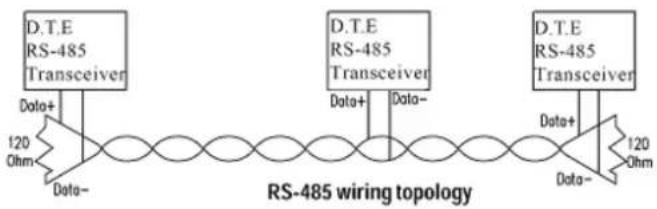
5.2.3 RS-485 Signal Wiring 45
Figure 5.1 RS-485 Wiring Topology .... 45
Appendix A Scale of Connectors 47
A.1 Connector Size Comparison.... 48
Figure A.1 DB9 Male.... 48
Figure A.2 DB25 Male 48
Figure A.3 DB37 Female 48
Figure A.4 DB62 Female 49
Figure A.5 DB78 Female 49
Chapter 1
Introduction
1.1 Description
1.1.1 PCI Express Bus
The PCI Express Bus is a high-speed, scalable I/O serial bus technology that is standard designed to replace the PCI bus. Thus, PCI Express has numerous advantages such as higher maximum system bus throughput, less I/O pin, more detailed error detection and reporting mechanism, and smaller physical footprint. Although, at the hardware level PCI slots and PCIe slots are not interchangeable, at the software level PCI Express preserves compatibility with PCI device drivers and OS.
PCI Express is a point-to-point connection, which means it does not share bandwidth but communicates directly with devices via a switch that directs data flow. By adding more lanes, scalable features can be achieved for greater bandwidth.
The PCIe link between PC and other devices can consist of 1 to 32 lanes. These numbers indicate the number of lanes you wish to have. For example, PCIe x16 has 16 lanes.
1.2 Features
PCI Express Card Features
■ PCI Express bus 2.0 compliant
■ Speeds up to 921.6 kbps for extremely fast data transmission
■ Supports any baud rate setting
2 x RS-232 or RS- 232/422/485 ports/ XR17V352 UART with 256-byte FIFOs
4 x RS-232 or RS- 232/422/485 ports/ XR17V354 UART with 256-byte FIFOs
8 x RS-232 or RS- 232/422/485 ports/ XR17V358 UART with 256-byte FIFOs
Operating systems supported: Windows 2000/XP/Vista/7/8/10, and Linux 2.4/2.6/3.x.x, QNX 6.5, VxWorks 6.9
Utility-ICOM Tools
1.3 Specifications
1.3.1 Bus Interface
The following table shows the bus specifications of the comm. cards.
| Bus interface Models | |
| PCI Express bus specifications 2.0 | PCIE-1602B, PCIE-1602C, PCIE-1604B, PCIE-1604C, PCIE-1610B, PCIE-1612B, PCIE-1612C, PCIE-1620A, PCIE-1622A, PCIE-1622B, PCIE-1622C |
| IRQ: All ports use the same IRQ assigned by PCI/ PCIe Plug-and-Play | |
| Data bits: 5, 6, 7, 8 | |
| Stop bits: 1, 1.5, 2 | |
| Parity: None, Even, Odd, Mark and Space | |
| Speed (bps): | |
| Model Criteria Speed (bps) | |
| PCI Express Series | A level 50~921.6 kbps |
| B level 50~921.6 kbps | |
Data Signals:
Table 1.1: Transmission Modes
BUS Interface Model name Ports Communication Interface
| RS-232 RS-422 RS-485 | |||||
| PCI Express | PCIE-1602B | 2 | V | V | V |
| PCIE-1602C 2 | V | V | V | ||
| PCIE-1604B | 2 | V | |||
| PCIE-1604C 2 | V | ||||
| PCIE-1610B | 4 | V | |||
| PCIE-1612B | 4 | V | V | V | |
| PCIE-1612C 4 | V | V | V | ||
| PCIE-1620A | 8 | V | |||
| PCIE-1622A | 8 | V | V | V | |
| PCIE-1622B | 8 | V | V | V | |
| PCIE-1622C 8 | V | V | V | ||
-
RS-232: TxD, RxD, RTS, CTS, DTR, DSR, DCD, RI
-
RS-422: Tx+, Tx-, Rx+, Rx-, CTS+, CTS-, RTS+, RTS-
-
RS-485: Data+, Data-
Dimensions
| Size | Model |
| 119.63 x 111 mm (4.71" x 4.4") | PCIE-1602B, PCIE-1602C, PCIE-1604B, PCIE-1604C |
| 168 x 111 mm (6.6" x 4.4") | PCIE-1610B, PCIE-1612B, PCIE-1612C, PCIE-1620A, PCIE-1622A, PCIE-1622B, PCIE-1622C |
Power Consumption
Table 1.2: Power Consumption
| Model name Typical Max |
| PCIE-1602B 260 mA @ +3.3 V 330mA @3.3V |
| PCIE-1602C 260 mA @ +3.3 V 450mA @3.3V |
| PCIE-1604B 260 mA @ +3.3 V 330mA @3.3V |
| PCIE-1604C 260 mA @ +3.3 V 450mA @3.3V |
| PCIE-1610B 260 mA @ +3.3 V 530mA @3.3V |
| PCIE-1612B 260 mA @ +3.3 V 530mA @3.3V |
| PCIE-1612C 260 mA @ +3.3 V 680mA @3.3V |
| PCIE-1620A 260 mA @ +3.3 V 880 mA @ 3.3 V |
| PCIE-1622A 260 mA @ +3.3 V 880 mA @ 3.3 V |
| PCIE-1622B 260 mA @ +3.3 V 880 mA @ 3.3 V |
| PCIE-1622C 260 mA @ +3.3 V 1250mA @3.3V |
■ Operating Temperature: -10 \~ 60°C (14 \~ 144°F)
Operating Humidity: 5 \~ 95% Relative Humidity, non-condensing
■ Storage Temperature: -25 \~ 85°C (-13\~185°F)
■ Current Value: 20mA (Standard)
Mode:
RS-232/422: Asynchronous, full duplex
RS-485: Asynchronous, half duplex
■ Baud-rate: 50 \~ 921.6 kbps
■ Transmission Distance:
RS-232<15m
RS-422/485 <1000m
1.3.2 Ordering Information
Table 1.3: Model List
| Product Description |
| PCIE-1602B 2-port RS-232/422/485 PCIe Comm. Card w/ Surge Protection |
| PCIE-1602C 2-port RS-232/422/485 PCIe Comm. Card w/ Surge & Isolation Protection |
| PCIE-1604B 2-port RS-232 PCIe Comm. Card w/ Surge Protection |
| PCIE-1604C 2-port RS-232 PCIe Comm. Card w/ Surge & Isolation Protection |
| PCIE-1610B 4-port RS-232 PCIe Comm. Card w/ Surge Protection w/ Surge Protection |
| PCIE-1612B 4-port RS-232/422/485 PCIe Comm. Card w/ Surge Protection |
| PCIE-1612C 4-port RS-232/422/485 PCIe Comm. Card w/ Surge & Isolation Protection |
| PCIE-1620A 8-port RS-232 PCIe Comm. Card |
| PCIE-1622A 8-port RS-232/422/485 PCIe Comm. Card |
| PCIE-1622B 8-port RS-232/422/485 PCIe Comm. Card w/ Surge Protection |
| PCIE-1622C 8-port RS-232/422/485 PCIe Comm. Card w/ Surge & Isolation Protection |
Table 1.4: PCIe Communication Cards Selection Guide
| Model Ports Comm. Interface Support | Protection | ||||
| Surge Isolation | |||||
| PCIE-1602 | B | RS-232/422/485 1000 V | |||
| C RS-232/422/485 1000 V | 3000 V | DC | |||
| PCIE-1604 | B | RS-232 | 1000 V | ||
| C RS-232 | 1000 V | 3000 V | DC | ||
| PCIE-1610 | B | RS-232 | 1000 V | ||
| PCIE-1612 | B | RS-232/422/485 1000 V | |||
| C RS-232/422/485 1000 V | 3000 V | DC | |||
| PCIE-1620 | A | RS-232 | |||
| PCIE-1622 | A | RS-232/422/485 | |||
| B | RS-232/422/485 1000 V | ||||
| C RS-232/422/485 1000 V | 3000 V | DC | |||
1.3.2.1 Accessories
■ OPT4A-AE: 30cm Male DB-37 to 4xMale DB9 Cable
■ OPT8C-AE: 1M Male DB-62 to 8xMale DB-25 Cable
■ OPT8H-AE: 1M Male DB-62 to 8xMale DB-9 Cable
■ OPT8J-AE: 1M Male DB-78 to 8xMale DB-9 Cable
■ OPT8HP: 1M double shield DB-62 to 8XDB-9 Cable
■ OPT8AP-AE: 8 port RS-232(DCE) ConnectionBox W/(F)DB25 CONN.
Chapter 2
Hardware
Configuration
2.1 Initial Inspection
- PCI/ PCI Express Communication card
- ICOM CD-ROM including:
a. User manual
b. Industrial Communication Driver
c. Utility tool
We carefully inspect our PCI/ PCI Express communication card mechanically and electrically before shipping. It should be free of marks and scratches and in perfect working condition on receipt.
As you unpack, check for any signs of shipping damage (damaged box, scratches, dents, etc.). Should any damage is found or fails to meet specifications, please notify our service department or your local sales representative immediately. Also the carrier should be notified. Retain the shipping carton and packing material for further inspections by the carrier.
After inspection we will make arrangements to repair or replace the unit.
When you handle the communication card, remove it from its protective packaging by holding the rear metal panel. Keep the anti-vibration packaging for further storage, as the card was removed from the PC.
Warning! Discharge your body's static electric charge by touching the back of the grounded chassis of the system unit (metal) before handling the board. You should avoid contact with materials that hold a static charge such as plastic, vinyl and styrofoam. Handle the board only by its edges to avoid static damage to its integrated circuits. Avoid touching the exposed circuit connectors. We also recommend that you use a grounded wrist strap and place the card on a static dissipative mat whenever you work with it.
2.2 Jumper and Switch Locations
2.2.1 PCIE-1602B

text_image
PCIE-1602B/1604B CN1 CN2 SW1 SW2 CN3 CN4Figure 2.1 PCIE-1602B Silk Screen
2.2.2 PCIE-1602C
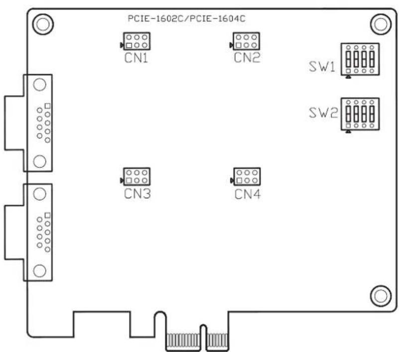
text_image
PCIE-1602C/PCIE-1604C CN1 CN2 SW1 SW2 CN3 CN4Figure 2.2 PCIE-1602C Silk Screen
2.2.3 PCIE-1612B

text_image
PCIE-1612B/PCIE-1610B CN5 CN1 CN6 CN2 SW1 CN8 CN4 SW2 CN7 CN3Figure 2.3 PCIE-1612B Silk Screen
2.2.4 PCIE-1612C
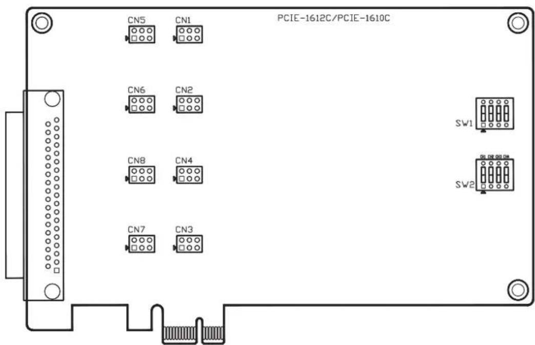
text_image
CN5 CN1 PCIE-1612C/PCIE-1610C CN6 CN2 CN8 CN4 CN7 CN3 SW1 SW2Figure 2.4 PCIE-1612C Silk Screen
2.2.5 PCIE-1620A/1622A/1622B
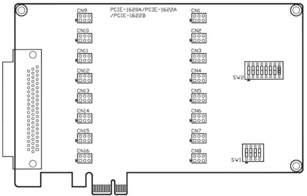
text_image
CN9 PCIE-1620A/PCIE-1622A /PCIE-1622B CN1 CN10 CN2 CN11 CN3 CN12 CN4 CN13 CN5 CN14 CN6 CN15 CN7 CN16 CN8 SW2 SW1Figure 2.5 PCIE-1620A/1622A/1622B Silk Screen
2.2.6 PCIE-1622C

text_image
PCIE-1622C CN9 CN1 CN10 CN2 CN11 CN3 CN12 CN4 CN13 CN5 CN14 CN6 CN15 CN7 CN16 CN8 SW2 SW1Figure 2.6 PCIE-1622C Silk Screen
2.3 Jumper Settings
This section shows how to set the jumpers to configure your card. It gives the card default configuration and your options for each jumper.
2.3.1 How to Set Jumpers
Configure the card to match the needs of your application by setting jumpers. A jumper is the simplest kind of electric switch. It consists of two metal pins and a small metal clip (often protected by a plastic cover) that slides over the pins to connect them. To “close” a jumper, connect the pins with the clip. To “open” a jumper, remove the clip.
You may find a pair of needle-nose pliers useful for setting the jumpers.
If you have any doubts about the best hardware configuration for your application, contact your local distributor or sales representative before making any changes.

Figure 2.7 How to Set Jumpers
2.3.2 Default Settings
The card is shipped with default settings. If you need to change these settings, however, refer to the following sections.
| PCIE-1600 Series Communication card Settings | |||
| Model Specifications | Default Setting | TX Enable Mode | Remarks |
| PCIE-1602B/ 1602C RS-232/422/485 RS-232 Auto | |||
| PCIE-1604B/1604C RS-232 RS-232 N/A | * means jumpers will be provided for terminator use and packed in PE bag along with the card inbox. | ||
| PCIE-1610B RS-232 RS-232 N/A | |||
| PCIE-1612B/1612C RS-232/422/485 RS-232 Auto | |||
| PCIE-1620A RS-232 RS-232 N/A | |||
| PCIE-1622A/1622B/ 1622C | RS-232/422/485 RS-232 Auto | ||
2.3.3 Mode Selection by Jumper/DIP Settings
2.3.3.1 RS-232/422/485 Selection ((for PCIE-1602B/1602C/1612B/1612C/1622A/1622B/1622C)
Should you wish to configure the PCIE communication card to operate in the RS-232 or RS422/RS-485 mode, you will locate jumpers at CN10 to CN17 to make connection as shown below.
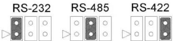
text_image
RS-232 RS-485 RS-422Figure 2.8 PCIE-1600 Series RS-232/422/485 Selection
Table 2.1: PCIE-1600 Series Operating Mode Jump Position
| Model CH1 CH2 CH3 CH4 CH5 CH6 CH7 CH8 | ||||||||
| PCIE-1602B CN1 CN3 | ||||||||
| PCIE-1602C CN1 CN3 | ||||||||
| PCIE-1612B CN1 CN2 CN3 CN4 | ||||||||
| PCIE-1612C CN1 CN2 CN3 CN4 | ||||||||
| PCIE-1622A | CN10 | CN11 | CN12 | CN13 | CN14 | CN15 | CN16 | CN17 |
| PCIE-1622B | CN10 | CN11 | CN12 | CN13 | CN14 | CN15 | CN16 | CN17 |
| PCIE-1622C CN1 CN2 CN3 CN4 CN5 CN6 | CN7 CN8 | |||||||
2.3.3.2 TX Enable mode selection
TX Enable mode is set by two, four or eight position DIP switches(SW2), one for each port.
If a switch is set to "On", the driver of the corresponding port is always enabled, master mode of RS-422 application. If a switch is set to "OFF", the driver is in auto direction control mode. The user must select a mode before beginning RS-422 applications.
Table 2.2: TX Enable Mode Selection
| Mode | Switch Position | Description |
| RS-422_Master | ON | TX always enabled |
| RS-422_Slave/RS-485 | OFF | Enabled auto direction control. |
2.3.3.3 Termination setup (for PCIE-1602B/1602C/1612B/1612C/1622A/1622B/1622C)
You can set termination resistors if necessary to match impedance. Each signal line (Tx, Rx) has a separate resistor.
Note!

Especially in fields with serious electric noise, setting termination resistors is helpful to stabilize communications. Make sure that both sides of the RS-485 bus have termination resistors. See details in Chapter 5.2.2 and 5.2.3.
Termination is recommended for use when designing a RS-422 interface.
RS422 mode with terminator resistor is 120ohm on standard condition. But the transmission condition is impacted by the impedance of cable length.

text_image
120Ω RX TX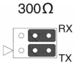
text_image
300Ω RX TXFigure 2.9 Impedance Selection (for PCIE-1600 Series)
Table 2.3: PCIE-1600 Series Impedance Selection Jumper Position
| Model CH1 CH2 CH3 CH4 CH5 CH6 CH7 CH8 | ||||||||
| PCIE-1602B CN2 CN4 | ||||||||
| PCIE-1602C CN2 CN4 | ||||||||
| PCIE-1612B CN5 CN6 CN7 CN8 | ||||||||
| PCIE-1612C CN5 CN6 CN7 CN8 | ||||||||
| PCIE-1622A CN2 CN3 CN4 CN5 CN6 CN7 CN8 CN9 | ||||||||
| PCIE-1622B CN2 CN3 CN4 CN5 CN6 CN7 CN8 CN9 | ||||||||
| PCIE-1622C | CN9 | CN10 | CN11 | CN12 | CN13 | CN14 | CN15 | CN16 |
2.4 Card Installation
Note!

We strongly recommend that you install the software driver before you install the hardware into your system, since this will guarantee a smooth and trouble-free installation process.
Turn off your PC's power supply whenever you install or remove the PCI/PCIe communication card or its cables. Static electricity can easily damage computer equipment. Ground yourself by touching the chassis of the computer (metal) before you touch any boards. See the static warning on Ch.2
- Install the driver; see chapter 3.1 and chapter 3.2.
- Turn off the computer and all peripheral devices (such as printers and monitors).
- Disconnect the power cord and any other cables from the back of the computer.
- Remove the PC's cover (refer to your user's guide if necessary).
- Install and plug the PCIe communication card on your PCIe BUS.
- Replace the PC's cover. Connect the cables you removed in step 3.
- Turn the computer power on.
- Driver will install PCIe Communication card automatically, see chapter 3.3 and 3.4 and 3.5.
- Test your COM port and verify if COM port could work normally, see chapter 4.
- Refer to the pin assignment and cabling for further information, see chapter 5.
Chapter 3
Driver Setup & Installation
3.1 Introduction
This chapter describes the driver installation, configuration, and removal procedures for Windows operating system. We strongly recommend installing the software driver before the hardware, since this will guarantee a smooth and trouble-free installation process.
3.2 Driver Setup
Windows operating system supports COM1 to COM256, meaning up to 256 serial ports. In order to fully utilize the advanced features of Windows operating system such as multiprocessing and multithreading, pure 32-bit Windows 2K/XP/Vista/7 and others, as afore indicated, device drivers are provided for the PCI/PCIe communication cards. All these drivers conform to the Win32 COMM API standard.
3.2.1 Steps for Operating System Driver Setup
Follow the steps below for the PCI/PCIe communication cards' windows operating system driver installation.
-
Insert your companion DVD-ROM disc into your DVD-ROM drive.
-
The driver setup program will be launched automatically. If the auto-play function is not enabled on your system, use Windows Explorer or the Windows Run command to execute autorun.exe on the companion DVD-ROM.

text_image
Advantech PCI ICOM Driver - InstallShield Wizard Preparing Setup Please wait while the InstallShield Wizard prepares the setup. Advantech PCI ICOM Driver Setup is preparing the InstallShield Wizard, which will guide you through the rest of the setup process. Please wait. InstallShield Cancel- After the setup program is launched, you'll see the following Screen.

text_image
Enabling an Intelligent Planet ADIANTECH DAQ Device Driver Disc 2014.2 CONTINUE- Click the Continue button and the catalogue select page appears. Then click the Installation button for installation.

text_image
ADVANTECH ICOM & CAN Driver CD V3.3 Installation Browse CD Contents View Our Website Contact Us Advantech Software Support CD-ROM features versatile drivers, device tools, examples and utilities for Advantech hardware. Quick Start Next Exit Enabling an Intelligent Planet- Choose the driver you want to install, then click the hyperlink.
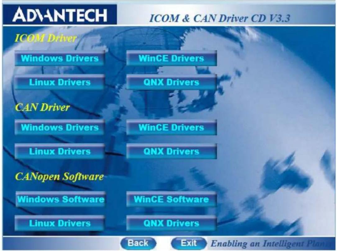
text_image
ADVANTECH ICOM & CAN Driver CD V3.3 ICOM Driver Windows Drivers WinCE Drivers Linux Drivers QNX Drivers CAN Driver Windows Drivers WinCE Drivers Linux Drivers QNX Drivers CANopen Software Windows Software WinCE Software Linux Drivers QNX Drivers Back Exit Enabling an Intelligent Plan
text_image
Advantech Setup Setup Status Advantech PCI ICOM Driver is configuring your new software installation. Installing C:\Program Files\Advantech\ICOM\PCI ICOM\InstallDriver_32Bit.exe InstallShield Cancel3.3 Driver Uninstall
- Insert the ICOM DVD and click the driver you want to uninstall.
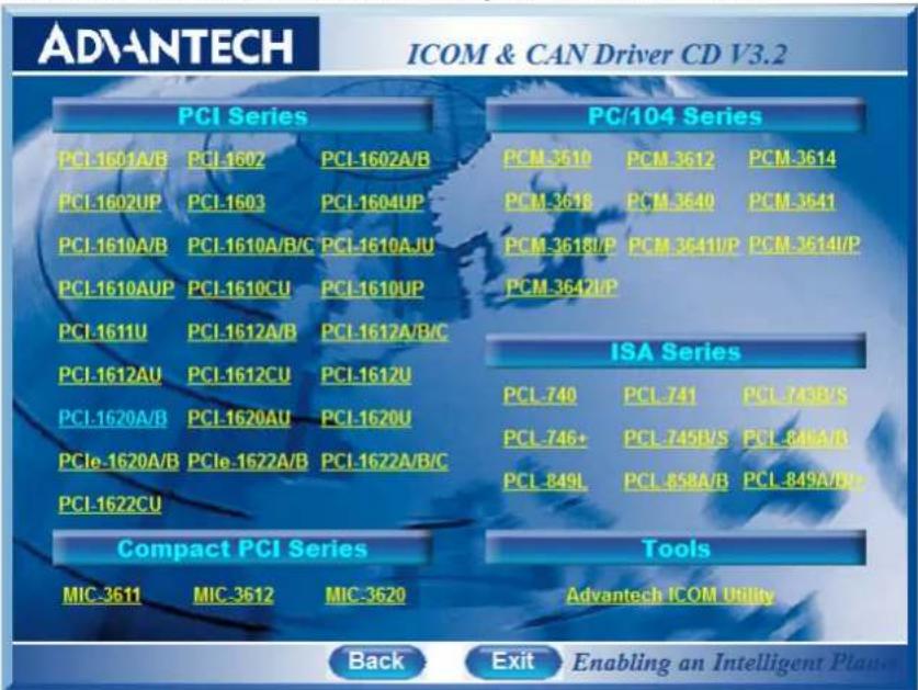
text_image
ADVANTECH ICOM & CAN Driver CD V3.2 PCI Series PCI-1601A/B PCI-1602 PCI-1602A/B PCI-1602UP PCI-1603 PCI-1604UP PCI-1610A/B PCI-1610A/B/C PCI-1610AJU PCI-1610AUP PCI-1610CU PCI-1610UP PCI-1611U PCI-1612A/B PCI-1612A/B/C PCI-1612AU PCI-1612CU PCI-1612U PCI-1620A/B PCI-1620AU PCI-1620U PCIe-1620A/B PCIe-1622A/B PCI-1622A/B/C PCI-1622CU PC/104 Series PCM_3510 PCM_3612 PCM_3614 PCM_3618 PCM_3640 PCM_3641 PCM_3618I/P PCM_3641I/P PCM_3614I/P PCM_3642I/P ISA Series PCL_740 PCL_741 PCL_743B/S PCL_746+ PCL_745B/S PCL_848A/B PCL_849L PCL_858A/B PCL_849A/B/P Compact PCI Series Tools MIC 3611 MIC 3612 MIC 3620 Advantech ICOM Utility Back Exit Enabling an Intelligent Planes- Choose "Modify" radio button if you want to save another driver. Or choose "Remove" radio button to remove all installed components.

text_image
Advantech Setup Welcome Modify, repair, or remove the program. Welcome to the Advantech PCI ICOM Driver Setup Maintenance program. This program lets you modify the current installation. Click one of the options below. Modify Select new program features to add or select currently installed features to remove. Repair Reinstall all program features installed by the previous setup. Remove Remove all installed features. InstallShield < Back Next > CancelChapter 4
ICOM Tools
4.1 Introduction
Advantech ICOM Tools is a convenient utility that has been designed to help you test the performance of ICOM cards through analyzing the port status. It features an easy to use graphical user interface that will soon make you familiar with testing via menu commands and toolbar buttons.
Advantech ICOM Tools is applicable to all series of Advantech ICOM cards, and can even be used with other third-party ICOM cards. It is included for free on the diskette or on the companion DVD-ROM with all Advantech Industrial Communication cards.
4.2 Installation
To begin installation, double-click the ICOM_Tools.exe program icon in the Tools folder or click the Advantech ICOM Utility hyperlink in the installation window to launch the ICOM Tools setup program. The setup program will copy the program files to the destination folder you choose or to the default installation path (i.e. C:\Program Files\Advantech\ICOM Tools). A program folder will be created in your Start/Programs menu. (Later you can just access the program through Start/Program/Advantech PCI Comm Tools/COM Examine Tool)
4.3 User Interface of ICOM Tools
4.3.1 Menu Bar
Port All Ports Help
On the Menu Bar you can select various menu commands to perform port-testing functions. You can also use the short-cut keys.
Port Submenu

Select: Select the ports you want to configure
Setup: Setup the configuration of a specific port
Close: Close a specific port
Run: Run the test on a specific port
Stop: Stop the test on a specific port
All Ports Submenu

Setup: Setup the configurations of all ports
Run: Run the test on all ports
Stop: Stop the test on all ports
Help Submenu Access Online help
4.3.2 Tool Bar

Using the Tool Bar buttons is a more intuitive way to implement the functions of ICOM Tools.
| Port Select: Selects the port(s) you want to perform testing on | |
| Port Setup: Sets up configuration of the port you have selected | |
| Port Close: Closes the port you have selected | |
| Port Run: Runs the port test on the port you have selected | |
| Port Stop: Stops the port test on the port you have selected | |
| All Ports Setup: Sets up the configuration of all ports not running test | |
| All Ports Run: Runs test on all ports | |
| All Ports Stop: Stops test on all ports | |
| Clear Message: Clears messages on Message Logo area and the Rx length information on the Performance Listing area |
4.3.3 Com Port Tab
Each Com Port tab represents a specific port you have selected for test and configuration. On the tab, you can see the Transfer Mode, Port Status, and Message Logo area.
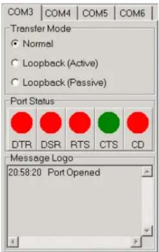
text_image
COM3 | COM4 | COM5 | COM6 Transfer Mode ● Normal ○ Loopback (Active) ○ Loopback (Passive) Port Status DTR DSR RTS CTS CD Message Logo 20:58:20 Port OpenedTransfer Modes
You can specify the transfer mode to be Normal, loopback (active) or loopback (passive).
Normal—allows data to be transmitted and received simultaneously. The data reception rate is helpful in identifying the performance of a communication card installed on your system.
Loopback- In loopback mode a series of special data will be transmitted, which are expected to appear on the receiving end. Using the loopback mode, you can check the integrity of received data and find whether any error occurred on the transmission line. The active loopback and passive loopback must work in pair to enable the loopback mode. When a port operates as active loopback mode, it will send data first and receive data later. Another port, which operates as passive loopback, will retransmit any received data on the Rx line and then send these data onto the Tx line. These two modes will form a logical loop and help to verify the integrity of data transmitted over the communication link.
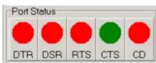
4.3.4 Port Status
text_image
Port Status DTR DSR RTS CTS CDDTR (data-terminal-ready)
DSR (data-set-ready)
RTS (request-to-send)
CTS (clear-to-send)
CD (carrier-detect)
For RS-232 specifications, DTR and RTS are for output signals and can be toggled on and off by double-clicking the labels (such as DTR, DSR, RTS, CTS, CD) under the red/green marks. However, if you are using RTS/CTS for flow control to run the test, you will see the RTS mark appear in black. This indicates that the RTS can no longer be toggled on/off since it is controlled by driver itself.

A black mark represents that the function is controlled by the driver itself and therefore not controllable by software.
4.3.5 Message Logo

text_image
Message Logo 20:58:20 Port OpenedOn the Message Logo area, you can see the relevant messages about the port(s) you have selected.
For information about specific messages in this area, please refer to Section 4.5, Messages on the Status Bar and Message Logo area.
4.3.6 Tx Slide Bar
The Tx Slide Bar allows you to control the overall system loading. You can adjust the transmission rate of your port(s) from 0% to 100%. Just drag the slide button along the track to adjust the transmission rate.

4.3.7 Performance Listing Area
On the performance listing area, you can see the relevant information, such as Rx Length (received packet byte length), Bytes/Sec (transmission rate) and Last Abnormal Status of each port running a test.

text_image
Performance Port Rx Length (Bytes/Sec) Last Abnormal Status4.3.8 Status Bar
READY 9600 N 8 2 NONE
The Status Bar is where you can glimpse the current information of the port you have selected. The Status Bar indicates whether the port is READY, RUNNING, BUSY or STOPPED, N/A PORT and the configuration information such as baud rate, data bit, stop bit, parity bit and flow control (represented as 1200 N 8 1 None) settings. Also we can see the duration of the test in hh:mm:ss format on the right.
For information about specific messages on this area, please refer to Section 4.5, Messages on the Status Bar and Message Logo area.
4.4 4.4 Using the ICOM Tools Utility
To launch the ICOM Tools testing utility, access Start/Programs/Advantech PCI Comm Tools/COM Examine Tools to start the port testing utility.
4.4.1 4.4.1 Port Selection
Follow the steps below to make your port selection:
- Launch ICOM Tools. You will first see the Program Window such as Figure 4.1. Since you haven't selected any port for testing yet, all you can see now is a blank window area.

text_image
Advantech - JCOM Tools Port: All Ports Help ADVANTECH. ICOM Tools www.advantech.comFigure 4.1 ICOM Tools program window
- Select the port(s) you want to test by the Port/Select menu command or by clicking the Port Select button on the Toolbar, and a dialog box such as Fig. 2 will appear.
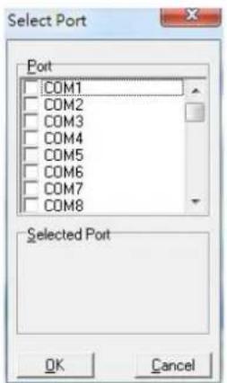
text_image
Select Port Port COM1 COM2 COM3 COM4 COM5 COM6 COM7 COM8 Selected Port OK CancelFigure 4.2 Select Port dialog box
Select the port(s) you want to perform test on from the checkboxes next to each COM port. You can either click the checkbox or double-click the name(s) of the port(s) to select/deselect port(s) to perform the test on. The port(s) you selected will immediately appear in the Selected Port field.
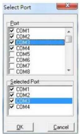
text_image
Select Port Port COM1 COM2 COM3 COM4 COM5 COM6 COM7 COM8 Selected Port COM1 COM2 COM3 COM4 OK CancelFigure 4.3 Ports You Select Will Appear in the Selected Port Checkbox Group Click OK to bring up the ICOM Tools User Interface such as below:
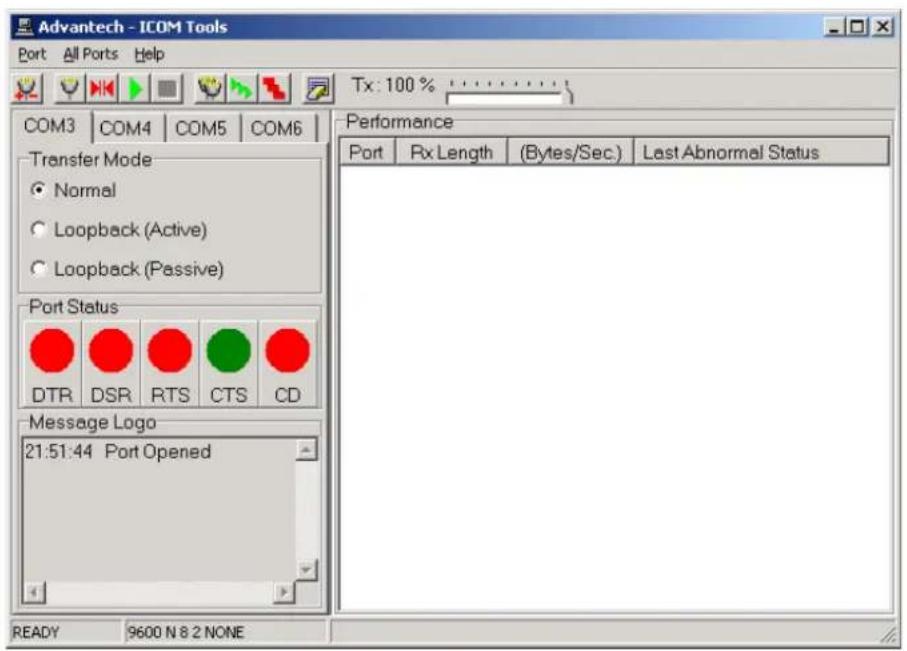
text_image
Advantech - ICOM Tools Port All Ports Help Tx: 100 % COM3 COM4 COM5 COM6 Transfer Mode Normal Loopback (Active) Loopback (Passive) Port Status DTR DSR RTS CTS CD Message Logo 21:51:44 Port Opened Performance Port Rx Length (Bytes/Sec.) Last Abnormal Status READY 9600 N 8 2 NONEFigure 4.4 Figure 4.4: ICOM Tools User Interface
4.4.2 Configuring a Port
You can choose to configure a specific port (or to configure all ports) before running your test. Just click a Com Port Tab to select the port you want to configure, and then click the Port Setup 🎨 button or use the Port/Setup menu command (or if you want to configure all ports at once, just click the All Ports Setup 🎨 button or access the All Ports/Setup menu command) to bring up the Configure Port dialog box such as below.
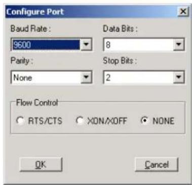
text_image
Configure Port Baud Rate : 9600 Data Bits : 8 Parity : None Stop Bits : 2 Flow Control RTS/CTS XON/XOFF NONE OK CancelFigure 4.5 Test Information on the Performance Listing Area
In the Configure Port dialog box, you can configure the Baud Rate, Data bits, Parity, Stop Bits and the flow control mode for that specific port (or for all ports). After you have configured all the settings you want to change, click OK to make this configuration active.
Note!

When using All Ports Setup button or All Ports/ Setup 📋 menu command to configure settings for all ports, you must take care to stop any ports
that are running test in order to configure them. If you do not stop the test running on a specific port, it won't be configured at all. That is, you get to configure only the ports that have been stopped.
Run the Test
After you have completed the configuration of the port(s), you can now start the test on the port you have selected by clicking the Run button or accessing the Port/Run menu command (or you want to run all ports at once, just click the All Ports Run button or access All Ports/Run menu command).
Once the test is started, you can see relevant test information of port performance on the performance listing area.
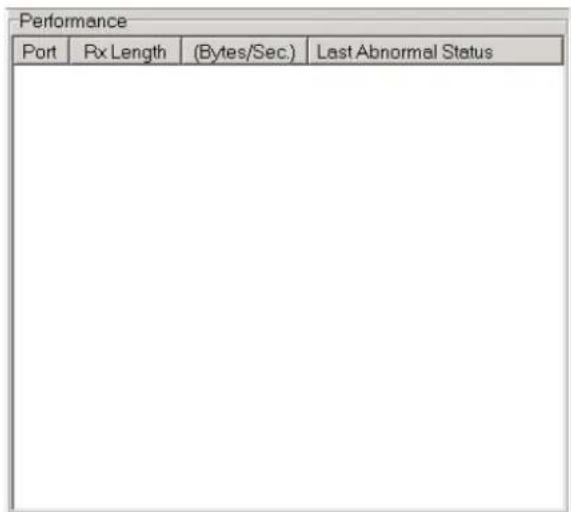
text_image
Performance Port Rx Length (Bytes/Sec.) Last Abnormal StatusFigure 4.6 Test Information on the Performance Listing Area
The Performance Listing Area
Port The com port number
Rx length Received packet length in bytes
Bytes/Sec Transmission rate in Bytes/Sec
Last Abnormal Status Last abnormal status
Stop the Test
If you want to stop the test on a specific port, just click Port Stop button or access Port/Stop menu command (or if you want to stop test on all ports, just click All Ports Stop button or access All Ports/Stop menu command).
You can restart the test by clicking the Run button or accessing the Port/Run menu command (or if you want to run all ports at once, just click the All Ports Run button or access All Ports/Run menu command).
4.4.3 Close Port
If you want to close a port, just select the Com Port tab and click Port Close button or access Port/Close menu command to close the port.
4.4.4 Exit the ICOM Tools utility
To exit the ICOM Tools utility, simply access Port/Exit menu command or click the Close button on the upper right corner of the program window.
4.5 Messages on Status Bar and Message Logo Area
Messages appearing on the Status Bar and Message Logo area are helpful in understanding specific information of your system settings and performance.
4.5.1 Status Bar Messages
BUSY: the port is currently used by another application.
FAIL: the configuration parameters are not accepted by the port
N/A PORT: the port is not available in the system
READY: the port is ready to run or to be configured.
RUNNING: the test is running on the port
STOPPED: the test running on the port has been stopped by the user
4.5.2 Message Logo Messages
Port Opened: The user has opened the port
Port Setup Fail: The user has set up the port configuration with parameters that are either incorrect or unsupported.
Port Running: The port is running a test
Port Stopped: The test is stopped on the port
Tx Starting/Tx Stopped: Transmitting starting/transmitting stop
Rx Starting/Rx Stopped: Receiving starting/receiving stop
Break Error: A break event has been detected on the port
Framing Error: A timing error (i.e. from start bit to stop bit) has been detected on the port
Port I/O Error: An incorrect I/O event has been detected on the port
Rx Overrun: Received data has been overwritten before being processed
Rx Buffer Full Error: The buffer on the receiving end is saturated so that newly arrived data are ignored
Tx Buffer Full Error: The buffer on the transmitting end is saturated so that the data transmitted by applications are ignored.
LB Error - %d: Data error is detected in loop back
LB Rx Pending: Loop back mode is waiting for incoming data
Data Setup Error: Parameter error in port configuration
Chapter 5
Pin Assignments and Wiring
5.1 Pin Assignments
5.1.1 PCIE-1602B/C
The following table and figure shows the pin assignments of two male DB9 connectors on the bracket for PCIE-1602B/PCIE-1602C in RS-232, RS-422 and RS-485 modes.
Table 5.1: PCIE-1602B/CMale DB9 on bracket
| Pin RS-232 RS-422 RS-485 | ||||
| 1 DCD Tx- Data- | ||||
| 2 | R x | D | T | x |
| 3 | T x | D | R | x |
| 4 | D T | R | R | x |
| 5 GND | GND | GND |  | |
| 6 DSR | RTS- | N/A | ||
| 7 | R T | S | R | T |
| 8 CTS | CTS+ | N/A | ||
| 9 | R I | C | T | S - N / A |
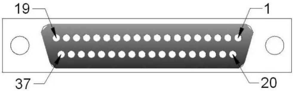
5.1.2 PCIE-1604B/C
The following table and figure shows the pin assignments of two male DB9 connectors on the bracket for PCIE-1604B and PCIE-1604C.
Table 5.2: PCIE-1604B/C Male DB9 on bracket
| Pin | RS-232 | 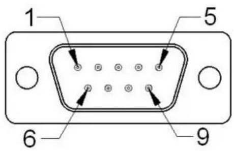 |
| 1 | DCD | |
| 2 | RxD | |
| 3 | TxD | |
| 4 | DTR | |
| 5 | GND | |
| 6 | DSR | |
| 7 | RTS | |
| 8 | CTS | |
| 9 | RI |
5.1.3 PCIe-1610B
The following tables and figures show the pin assignments of 1 female DB37 connector on the bracket to male DB9/DB25 for PCIe-1610B cards.
| Table 5.3: PCIE-1610B Male DB9 on cable | ||
| Pin RS-232 | 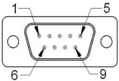 | |
| 1 DCD | ||
| 2 | RxD | |
| 3 | TxD | |
| 4 | DTR | |
| 5 | GND | |
| 6 | DSR | |
| 7 | RTS | |
| 8 | CTS | |
| 9 | RI | |
| Table 5.4: PCIE-1610B Male DB25 on cable | ||
| Pin RS-232 | 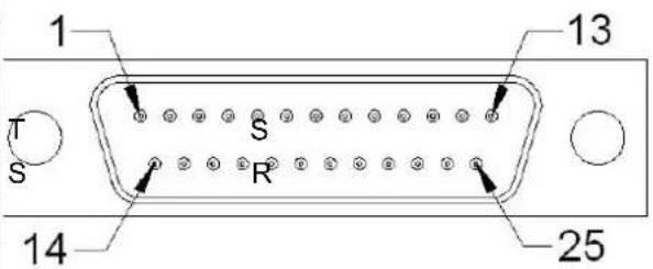 | |
| 2 TxD | ||
| 3 | RxD | |
| 4 | RTS | |
| 5 | C | |
| 6 | D | |
| 7 | GND | |
| 8 DCD | ||
| 20 DTR | ||
| 22 RI | ||
Table 5.5: PCIE-1610B Female DB37 on bracket
| Pin RS-232 Pin RS-232 | |||
| 1 - 20 3_RI | |||
| 2 3_DCD 21 3_DTR | |||
| 3 3_GND 22 3_DSR | |||
| 4 3_CTS 23 3_RTS | |||
| 5 3_RxD 24 3_TxD | |||
| 6 | 4 | _ | R |
| 7 4_DTR 26 4_GND | |||
| 8 4_DSR 27 4_CTS | |||
| 9 4_RTS 28 4_RxD | |||
| 10 4_TxD | |||
| 29 2_RI | |||
| 11 | 2_DCD | 30 2_DTR | |
| 12 2_GND 31 2_DSR | |||
| 13 2_CTS | 32 2_RTS | ||
| 14 2_RxD | 33 2_TxD | ||
| 15 1_RI | 34 1_DCD | ||
| 16 1_DTR 35 1_GND | |||
| 17 1_DSR 36 1_CTS | |||
| 18 1_RTS | 37 1_RxD | ||
| 19 1_TxD | |||
text_image
19 1 37 205.1.4 PCIe-1612B/C
The following tables and figures show the pin assignments of 1 female DB37 connector on the bracket to male DB9/DB26 for the PCIe-1612B/C cards in RS-232, RS-422 and RS-485 modes.
Table 5.6: PCIE-1612B/C Male DB9 on cable
| Pin RS-23 | 2 RS-422 | RS-485 | RR | 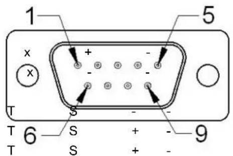 | |
| 1 DCD Tx- | Data- | ||||
| 2 RxD Tx+ | Data+ | ||||
| 3 | T | x | D | ||
| 4 | D | T | R | ||
| 5 GND | GND | GND | |||
| 6 | D | S | R R | ||
| 7 | R | T | S R | ||
| 8 | C | T | S C | ||
| 9 | R | I | C | T | S - - |
Table 5.7: PCIE-1612B/C Male DB25 on cable
| Pin | RS-232 | Pin | RS-232 | Pin | RS-232 |
| 1 | 1_TxD | 16 | 1_CTS | 31 | 1_DCD |
| 2 | 1_RxD | 17 | 1_DTR | 32 | 1_RI |
| 3 | 1_RTS | 18 | 1_DSR | 33 | 1_GND |
| 4 | - | 19 | - | 34 | - |
| 5 | 1_TxD | 20 | 2_CTS | 35 | 2_DCD |
| 6 | 2_RxD | 21 | 2_DTR | 36 | 2_RI |
| 7 | 2_RTS | 22 | 2_DSR | 37 | 2_GND |
| 8 | - | 23 | - | 38 | - |
| 9 | 3_TxD | 24 | 3_CTS | 39 | 3_DCD |
| 10 | 3_RxD | 25 | 3_DTR | 40 | 3_RI |
| 11 | 3_RTS | 26 | 3_DSR | 41 | 3_GND |
| 12 | - | 27 | - | ||
| 13 | 4_TxD | 28 | 4_CTS | 42 | 4_DCD |
| 14 | 4_RxD | 29 | 4_DTR | 43 | 4_RI |
| 15 | 4_RTS | 30 | 4_DSR | 44 | 4_GND |

text_image
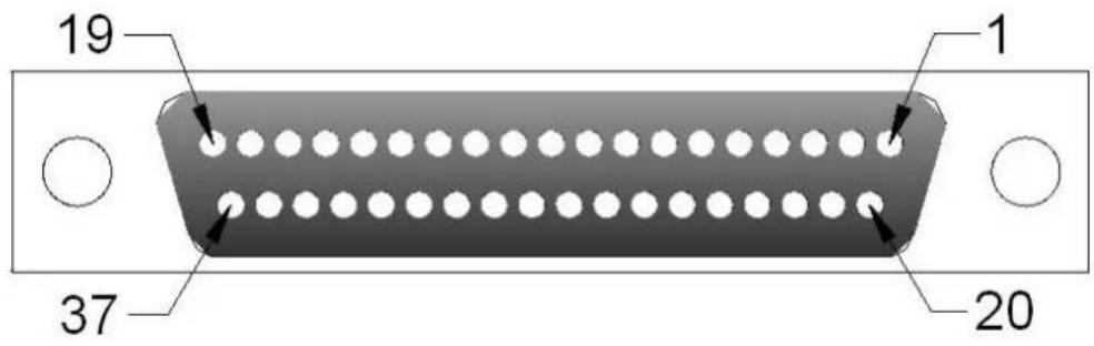
1 13 14 25Table 5.8: PCIE-1612B/C Female DB37 on bracket
| Pin RS-232 | RS-422 | RS-485 | Pin RS-232 | RS-422 | RS-485 | |||
| 1---20 3 | RI 3_CTS- | |||||||
| 2 3_DCD 3 | _TxD- 3_Data- | 21 3_DTR 3_RxD- | ||||||
| 3 3_GND 3 | _GND 3_GND 22 3_DS | SR 3_RTS- | ||||||
| 4 3_CTS 3 | _CTS+ - 23 | 3_RTS | 3_RTS+ - | |||||
| 5 | 3_RxD | 3_TxD+ | 3_Data+ | 24 | 3_TxD | 3_RxD+ | - | |
| 6 4_RI 4_CTS- - 25 4_ | DCD 4_TxD- 4_Data- | |||||||
| 7 4_DTR 4 | _RxD - | 26 4_GND | 4_GND | 4_GND | ||||
| 8 4_DSR 4 | _RTS- - | 27 4_CTS 4_CTS+ - | ||||||
| 9 | 4_RTS | 4_RTS+ | - | 28 | 4_RxD | 4_TxD+ | 4_Data+ | |
| 10 4_TxD | 4_RxD+ | - | ||||||
| 29 2_RI 2_CTS- - | ||||||||
| 11 | 2_DCD 2_TxD- 2_Data- | 30 2_DTR 2_RxD- - | ||||||
| 12 2_GND | 2_GND 2_GND 31 | 2_DSR 2_RTS- | ||||||
| 13 2_CTS | 2_CTS+ | 32 2_RTS | 2_RTS+ | - | ||||
| 14 | 2_RxD | 2_TxD+ | 2_Data+ | 33 | 2_TxD | 2_RxD+ | - | |
| 15 1_RI 1 | CTS- - 34 1 | _DCD 1_TxD- 1_Data- | ||||||
| 16 1_DTR | 1_RxD | - 35 1_GND | 1_GND | 1_GND | ||||
| 17 1_DSR | 1_RTS- | - 36 1_CTS 1_CTS+ - | ||||||
| 18 | 1_RTS | 1_RTS+ | - | 37 | 1_RxD | 1_TxD+ | 1_Data+ | |
| 19 1_TxD | 1_RxD+ | + | ||||||
text_image
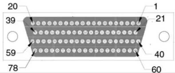
19 1 37 205.1.5 PCIE-1620A and PCIE-1622A/B
The following tables and figures show the pin assignments of 1 female DB62 connector on the bracket to DB9 for the PCIE-1620A and PCIE-1622A/B cards.
| Table 5.9: PCIE-1620A, PCIE-1622A/B Female DB62 on bracket | |||||||
| Pin RS-232 | RS-422 RS | RS-485 Pin RS | RS-232 RS-422 RS-485 | ||||
| 1 1_TX 1_RX+ - 32 GND GND GND | |||||||
| 2 1_DTR 1_RX- - 33 5_TX 5_RX+ | |||||||
| 3 2_RX 2_TX+ 2_Data+ 34 | 5_DTR 5_RX- - | ||||||
| 4 2_DSR | -- 35 6_RX 6_TX+ | 6_Data+ | |||||
| 5 | 2_DCD | 2_TX- | 2_Data- | 36 | 6_DSR | - | - |
| 6 | 3_TX | 3_RX+ | - | 37 | 6_DCD | 6_TX- | 6_Data- |
| 7 3_DTR 3_RX - 38 7_TX 7_RX+ - | |||||||
| 8 4_RX 4_TX+ 4_Data+ 39 | 7_DTR 7-RX- _ | ||||||
| 9 4_DSR | -- 40 GND GND GND | ||||||
| 10 | 4_DCD | 4_TX- | 4_Data- | 41 | 8_TX | 8_RX+ | - |
| 11 | 5_RX 5_TX+ 5_Data+ 42 8_DTR 8_RX- - | ||||||
| 12 5_DSR | -- 43 1_CTS -- | ||||||
| 13 | 5_DCD | 5_TX- | 5_Data- | 44 | 1_RTS | - | - |
| 14 6_TX | 6_RX+ - 45 GND GND GND | ||||||
| 15 6_DTR | 6_RX- - 46 | 2_CTS -- | |||||
| 16 | 7_RX | 7_TX+ | 7_Data+ | 47 | 2_RTS | - | - |
| 17 | 7_DSR | -- 48 3_CTS -- | |||||
| 18 | 7_DCD | 7_TX- | 7_Data- | 49 | 3_RTS | - | - |
| 19 | 8_RX | 8_TX+ | 8_Data+ | 50 | GND | GND | GND |
| 20 | 8_DSR | -- 51 4_CTS -- | |||||
| 21 | 8_DCD | 8_TX- | 8_Data- | 52 | 4_RTS | - | - |
| 22 | 1_RX | 1_TX- | 1_Data+ | 53 | 5_CTS | - | - |
| 23 | 1_DSR | -- 54 5_RTS -- | |||||
| 24 | 1_DCD | 1_TX- | 1_Data- | 55 | GND | GND | GND |
| 25 | 2_TX 2_RX+ - 56 | 6_CTS | -- | ||||
| 26 | 2_DTR 2_RX- - 57 | 6_RTS | -- | ||||
| 27 | 3_RX | 3_TX+ | 3_Data+ | 58 | GND | GND | GND |
| 28 | 3_DSR | -- 59 7_CTS -- | |||||
| 29 | 3_DCD | 3_TX- | 3_Data- | 60 | 7_RTS | - | - |
| 30 | 4_TX 4_RX+ - 61 | 8_CTS | -- | ||||
| 31 | 4_DTR 4_RX- - 62 | 8_RTS | -- | ||||
text_image
21 1 22 42 62 43Table 5.10: PCIE-1622A/B Male DB9 on cable
| Pin RS-232 RS-422 | RS-485 | ||
| 1 DCD TX- Data- | |||
| 2 | R | x | D |
| 3 | T | x | D |
| 4 | D | T | R |
| 5 GND GND GND | |||
| 6 | D | S | R |
| 7 | R | T | S - |
| 8 | C | T | S - |
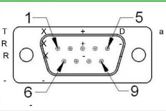
text_image
1 T R R - 6 - + - X + - D a 5 9Table 5.11: PCIE-1620A Male DB9 on cable
| Pin | RS-232 |
| 1 | DCD |
| 2 | RxD |
| 3 | TxD |
| 4 | DTR |
| 5 | GND |
| 6 | DSR |
| 7 | RTS |
| 8 | CTS |
| 9 | RI |
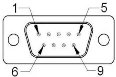
text_image
1 5 6 9Table 5.12: PCIE-1622A/B Male DB25 on cable
| Pin | RS-232 | RS-422 | RS-485 |
| 1 | DCD | TX- | Data- |
| 2 | RxD | TX+ | Data+ |
| 3 | TxD | RX+ | - |
| 4 | DTR | RX- | - |
| 5 | GND | GND | GND |
| 6 | DSR | - | - |
| 7 | RTS | - | - |
| 8 | CTS | - | - |
| 20 | DTR | - | - |

text_image
1 13 14 255.1.6 PCIE-1622C
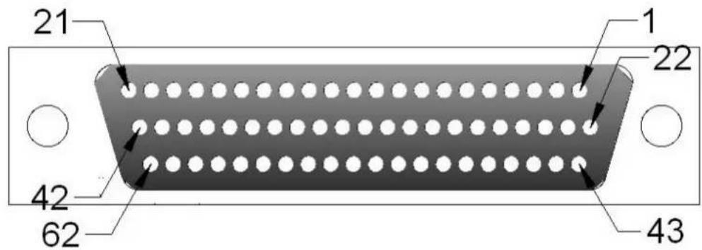
The following table and figure show the pin assignments of 1 female DB78 connector on the bracket to DB9 for the PCIE-1622C card in RS-232, RS-422 and RS-485 modes.
| Table 5.13: PCIe-1622C Male DB9 on cable | ||||
| Pin RS-232 RS-422 RS-485 | ||||
| 1 DCD Tx- Data- | ||||
| 2 | R | x | D T | |
| 3 | T | x | D R | |
| 4 | D | T | R R | |
| 5 | G | N | D G | |
| 6 DSR | RTS-N/A | |||
| 7 | R | T | S R | |
| 8 CTS CTS+ N/A | ||||
| 9 | R | I | C T | S - N / A |
Table 5.14: PCIe-1622C Female DB78 on bracket
Pin RS-232 RS-422 RS-485 Pin RS-232 RS-422 RS-485
| 1 8_GND 8_GND 8_GND 40 8_DCD 8_TxD- 8_Data- | ||||||
| 2 8_DSR 8_RTS- - 41 8_RxD 8_TxD+ 8_Data+ | ||||||
| 3 8_RTS 8_RTS+ - 42 7_GND 7_GND 7_GND | ||||||
| 4 7_DSR 7_RTS- - 43 7_DCD 7_TxD- 7_Data- | ||||||
| 5 | 7_RTS | 7_RTS+ | - | 44 | 7_RxD | 7_TxD+ 7_Data+ |
| 6 6_DSR | 6_RTS- - 45 6_DCD 6_TxD- 6_Data- | |||||
| 7 | 6_RTS | 6_RTS+ | - | 46 | 6_RxD | 6_TxD+ 6_Data+ |
| 8- | - | - 47 5_GND | 5_GND 5_GND | |||
| 9 5_DSR | 5_RTS- - 48 5_DCD 5_TxD- 5_Data- | |||||
| 10 | 5_RTS | 5_RTS+ | - | 49 | 5_RxD | 5_TxD+ 5_Data+ |
| 11 | 4_DSR | 4_RTS- - 50 4_DCD 4_TxD- 4_Data- | ||||
| 12 | 4_RTS | 4_RTS+ | - | 51 | 4_RxD | 4_TxD+ 4_Data+ |
| 13 | - | - | - | 52 | 3_GND | 3_GND 3_GND |
| 14 | 3_DSR | 3_RTS- - 53 3_DCD 3_TxD- 3_Data- | ||||
| 15 | 3_RTS | 3_RTS+ | - | 54 | 3_RxD | 3_TxD+ 3_Data+ |
| 16 | 2_DSR | 2_RTS- - 55 2_DCD 2_TxD- 2_Data- | ||||
| 17 | 2_RTS | 2_RTS+ | - | 56 | 2_RxD | 2_TxD+ 2_Data+ |
| 18 | - | - | - | 57 | 1_GND | 1_GND 1_GND |
| 19 | 1_DSR | 1_RTS- - 58 1_DCD 1_TxD- 1_Data- | ||||
| 20 | 1_RTS | 1_RTS+ | - | 59 | 1_RxD | 1_TxD+ 1_Data+ |
| 21 | 8_CTS | 8_CTS+ | - | 60 | 8_TxD | 8_RxD+ - |
| 22 | 8_RI | 8_CTS- | - | 61 | 8_DTR | 8_RxD- - |
| 23 | 7_CTS | 7_CTS+ | - | 62 | 7_TxD | 7_RxD+ - |
| 24 | 7_RI | 7_CTS- | - | 63 | 7_DTR | 7_RxD- - |
| 25 | - | - | - | 64 | 6_GND | 6_GND 6_GND |
| 26 | 6_CTS | 6_CTS+ | - | 65 | 6_TxD | 6_RxD+ - |
| 27 | 6_RI | 6_CTS- | - | 66 | 6_DTR | 6_RxD- - |
| 28 | 5_CTS | 5_CTS+ | - | 67 | 5_TxD | 5_RxD+ - |
| 29 | 5_RI | 5_CTS- | - | 68 | 5_DTR | 5_RxD- - |
| 30 | - | - | - | 69 | 4_GND | 4_GND 4_GND |
| 31 | 4_CTS | 4_CTS+ | - | 70 | 4_TxD | 4_RxD+ - |
| 32 | 4_RI | 4_CTS- | - | 71 | 4_DTR | 4_RxD- - |
| 33 | 3_CTS | 3_CTS+ | - | 72 | 3_TxD | 3_RxD+ - |
| 34 | 3_RI | 3_CTS- | - | 73 | 3_DTR | 3_RxD- - |
| 35 | - | - | - | 74 | 2_GND | 2_GND 2_GND |
| 36 | 2_CTS | 2_CTS+ | - | 75 | 2_TxD | 2_RxD+ - |
| 37 | 2_RI | 2_CTS- | - | 76 | 2_DTR | 2_RxD- - |
| 38 | 1_CTS | 1_CTS+ | - | 77 | 1_TxD | 1_RxD+ - |
| 39 | 1_RI | 1_CTS- | - | 78 | 1_DTR | 1_RxD- - |
text_image
20 39 59 78 1 21 40 605.2 Wiring
5.2.1 RS-232 Signal Wiring
Since the RS-232 interface is not strictly defined, many devices have their own connection methods which may ignore some signal lines or reserved lines for other functions. It is best to refer to the user's manual of your device for installation instructions. You may find the following helpful.
In general, DTE (Data Terminal Equipment) refers to the device that is leading the communication. Examples include PC's, terminals and some printers. DCE refers to the device being communicated with or controlled. Examples include modems, DSU's (digital service units), printers and lab/factory equipment.
In some situations you may be able to get by with just three lines: data on TXD, a signal ground and a handshaking line. Examples are printer or plotter connections, troubleshooting and situations where you require only one-wire communication.
| Table 5.15: Terminal or PC (DTE) Connections | |||
| DB-25 Male DB-25 Male or Female: Terminal | |||
| Pin Signal Pin Signal | |||
| 2 | T | x | D |
| 3 | R | x | D |
| 4 | R | T | S |
| 5 | C | T | S |
| 6 | D | S | R 2 |
| 7 | G | N | D 7 |
| 20 | DTR | 6 | DSR |
| 8 | DCD | 8 | DCD |
3 2 5 4
| Table 5.16: Modem Connections | |||
| DB-25 Male | Modem (DCE) | ||
| Pin | Signal | Pin | Signal |
| 2 | T | x | D 3 |
| 3 | R | x | D 2 |
| 4 | R | TS | 5 |
| 5 | C | TS | 4 |
| 6 | D | SR 2 | 0 |
| 7 | G | ND 7 | 0 |
| 20 | DTR | 6 | DSR |
| 8 | DCD | 8 | DCD |
C RT
For DTE to DCE connections, use a straight through cable (i.e., you don't have to reverse lines 2 and 3, lines 4 and 5, and lines 6 and 20 since, in general, the DCE RS-232 interfaces are reversed themselves).
| Table 5.17: Terminal without Handshake | |||
| DB-25 Male Terminal, PC (DTE) | |||
| Pin Signal Pin Signal | |||
| 2 | T | x | D |
| 3 RxD 2 TxD | |||
| 4 | RTS | ||
| 5 | CTS | ||
| 7 | G | N | D |
| 6 | DSR | ||
| 20 DTR | |||
| 8 DCD | |||
Therefore, if you are not using CTS, RTS, DSR, DTR and DCD signals, short pins 4 and 5 together, and please short pins 6, 8, and 20 together.
5.2.2 RS-422 Signal Wiring
The RS-422 interface wiring is based on one-on-one principles. The transmit lines on one side connect to the receive lines on the other side, and vice versa. With RS-422, you can transmit and receive data simultaneously (full duplex). The connections are as follows:
| Table 5.18: RS-422 DB9 Pin Assignment | |||
| DTE (Male DB-9) | Terminal DTE | ||
| Pin Signal Pin Signal | |||
| 1 TxD- | 1 RxD- | ||
| 2 TxD+ | 2 RxD+ | ||
| 3 | R | x | D |
| 4 | R | x | D |
| 5 | G | N | D |
| 6 | R | T | S |
| 7 | R | T | S |
| 8 | C | T | S |
Termination Resistors Setup
Termination resistors are on-board and can be selected by jumper for 120 or 300 Ohms. Each pair of signal lines has a separate resistor (RxD+/-, TxD+/-).
5.2.3 RS-485 Signal Wiring
The RS-485 standard supports half-duplex communication. This means that just two wires are needed to both transmit and receive data. Handshaking signals (such as RTS, Request To Send) are normally used to control the direction of the data flow and to switch the transmission accordingly. In RS-485 mode, the PCIe-1602/1612/1622 cards automatically sense the direction of the data flow and switch the transmission direction — no handshaking is necessary. This means a user can build an RS-485 network with just two wires. This RS-485 control is completely transparent to the user. The software written for half duplex RS-485 works without any modification.
flowchart
graph LR
    A["Data+"] --> B["RS-485 Transceiver"]
    B --> C["Data-"]
    C --> D["RS-485 Wiring Topology"]
    D --> E["Data+"]
    E --> F["RS-485 Transceiver"]
    F --> G["Data-"]
    G --> H["RS-485 Transceiver"]
    H --> I["Data+"]
    I --> J["RS-485 Transceiver"]
    J --> K["120 Ohm"]
    style D fill:#f9f,stroke:#333
    style F fill:#f9f,stroke:#333
    style H fill:#f9f,stroke:#333
Figure 5.1 RS-485 Wiring Topology
Termination Resistor Setup
Termination resistors are on-board and can be selected by jumper for 120 or 300 Ohms.
Appendix A
Scale of Connectors
A.1 Connector Size Comparrison

text_image
24.99±0.25 2.775±0.05 8.30±0.25 3.85±0.30 11.06±0.15 6.945±0.15 30.80±0.35 2.84±0.10 12.50±0.25 2-#4-40UNCFigure A.1 DB9 Male
text_image
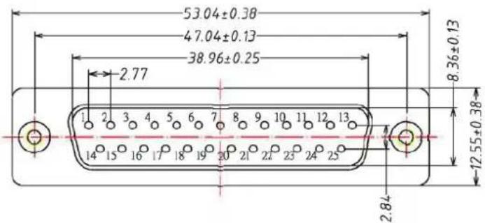
53.04±0.38 47.04±0.13 38.96±0.25 2.77 8.36±0.13 14 15 16 17 18 19 20 21 22 23 24 25 2.84 -12.55±0.38Figure A.2 DB25 Male
POSITION A±0.20 B±0.20 C±0.38 D
37 PIN 54.80 63.50 69.40 49.86

text_image
C B A 2.77 #4-40UNC*2 5 9 6 7.9 12.50 4 2.84Figure A.3 DB37 Female
| P | O | S | I | T | I | O | N |
| 62 PIN | 54.8 | 63.50 | 69.40 | 2.41 | 1.20 | 7.00 |

text_image
C B A PIN #9 7.9 12.5 (1.98) E D UNC 4#40*2Figure A.4 DB62 Female
| POSITION A B C D1 D2 E F | |||||||
| 78 PIN | 67.16±0.38 | 61.11±0.25 | 52.40±0.20 | 2.41 | 2.08 | 10.72±0.25 | 14.1±0.25 |

text_image
A B C D1 20 39 59 78 1 21 40 60 D2 E FFigure A.5 DB78 Female
ADVANTECH
Enabling an Intelligent Planet
www.advantech.com
Please verify specifications before quoting. This guide is intended for reference purposes only.
All product specifications are subject to change without notice.
No part of this publication may be reproduced in any form or by any means, electronic, photocopying, recording or otherwise, without prior written permission of the publisher.
All brand and product names are trademarks or registered trademarks of their respective companies.
© Advantech Co., Ltd. 2015