
FCBN510QE2C05 - Câble pour ordinateur et périphérique Finisar - Notice d'utilisation et mode d'emploi gratuit
Retrouvez gratuitement la notice de l'appareil FCBN510QE2C05 Finisar au format PDF.
| Type de produit | Câble actif optique Quadwire® 40 Gb/s avec répartition (breakout) de QSFP+ vers 4x SFP+ |
| Modèle | FCBN510QE2C05 |
| Marque | Finisar |
| Longueur | 5 mètres |
| Diamètre du câble (partie commune) | 3,0 à 3,6 mm |
| Diamètre du câble (partie divisée) | 1,8 à 2,2 mm |
| Connecteurs | 1x QSFP+ (38 broches) et 4x SFP+ (20 broches) |
| Débit de données agrégé | Jusqu'à 42 Gb/s |
| Débit par voie | 10,3125 Gb/s |
| Nombre de voies | 4 émission et 4 réception |
| Alimentation électrique (QSFP+) | Moins de 1,3 W |
| Alimentation électrique (chaque SFP+) | Moins de 1 W |
| Tension d'alimentation | 3,3 V ± 5 % |
| Température de fonctionnement | 0 °C à 70 °C |
| Température de stockage | -10 °C à 75 °C |
| Type de fibre | Multimode, plénum (OFNP) |
| Rayon de courbure minimal | 60 mm (105 mm près des connecteurs) |
| Conformités | RoHS-6, sécurité laser Classe 1 (IEC 60825-1) |
| Fonctions principales | Transmission 40GbE, breakout, interface I2C, enfichable à chaud |
| Entretien et nettoyage | Nettoyer les connecteurs optiques avec un chiffon non pelucheux et de l'alcool isopropylique si nécessaire. |
| Sécurité | Éviter toute exposition au faisceau laser. Utiliser conformément aux normes IEC 60825-1. |
| Pièces détachées et réparabilité | Aucune pièce détachable. Le câble n'est pas réparable, remplacer l'ensemble. |
| Poids estimé | Environ 200 g |
FOIRE AUX QUESTIONS - FCBN510QE2C05 Finisar
Questions des utilisateurs sur FCBN510QE2C05 Finisar
0 question sur cet appareil. Repondez a celles que vous connaissez ou posez la votre.
Poser une nouvelle question sur cet appareil
Téléchargez la notice de votre Câble pour ordinateur et périphérique au format PDF gratuitement ! Retrouvez votre notice FCBN510QE2C05 - Finisar et reprennez votre appareil électronique en main. Sur cette page sont publiés tous les documents nécessaires à l'utilisation de votre appareil FCBN510QE2C05 de la marque Finisar.
MODE D'EMPLOI FCBN510QE2C05 Finisar
Preliminary Product Specification
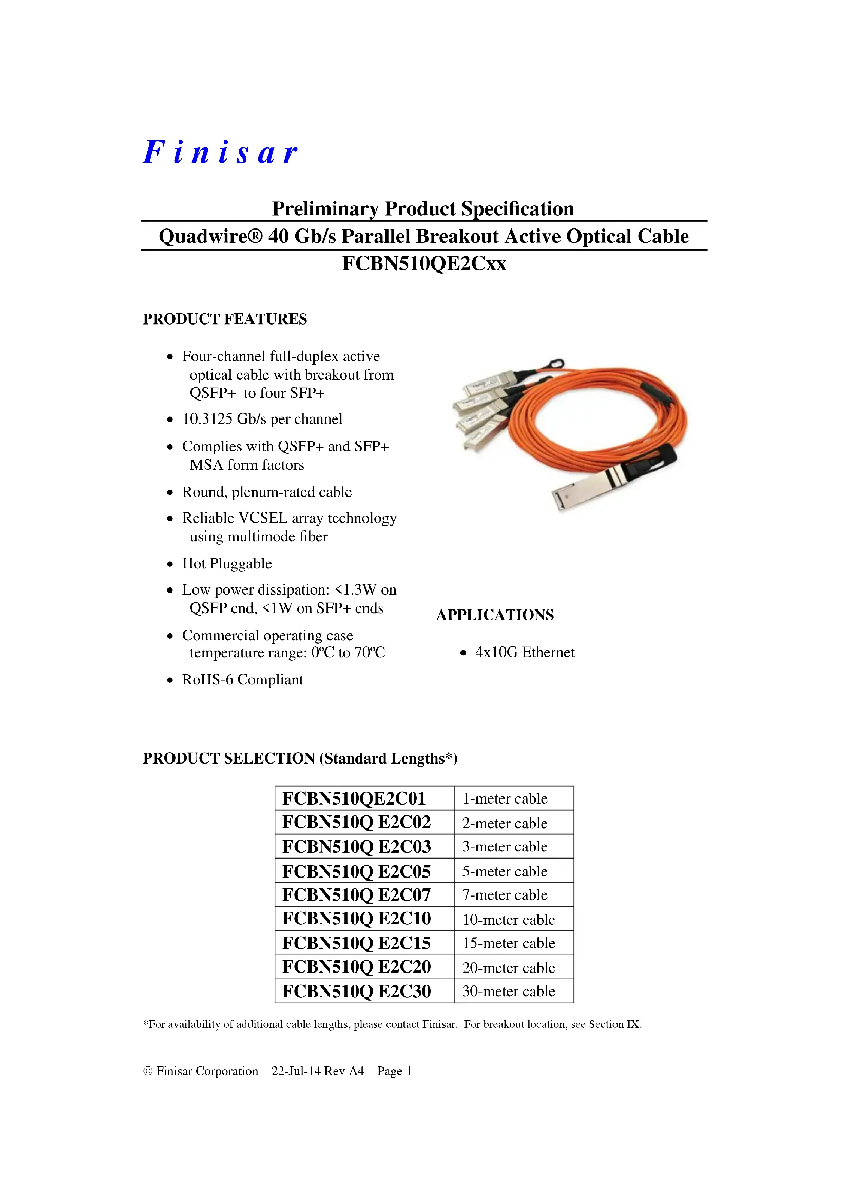
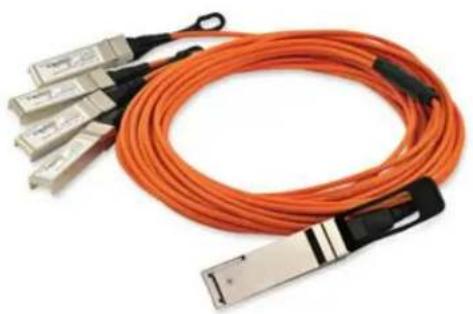
Quadwire® 40 Gb/s Parallel Breakout Active Optical Cable
FCBN510QE2Cxx
PRODUCT FEATURES
Four-channel full-duplex active optical cable with breakout from QSFP+ to four SFP+
10.3125 Gb/s per channel
- Complies with QSFP+ and SFP+
MSA form factors
- Round, plenum-rated cable
- Reliable VCSEL array technology using multimode fiber
- Hot Pluggable
- Low power dissipation: < 1.3W on QSFP end, < 1W on SFP + ends
- Commercial operating case temperature range: 0^ to 70^
RoHS-6 Compliant
APPLICATIONS
4x10G Ethernet
PRODUCT SELECTION (Standard Lengths*)
| FCBN510QE2C01 | 1-meter cable |
| FCBN510Q E2C02 | 2-meter cable |
| FCBN510Q E2C03 | 3-meter cable |
| FCBN510Q E2C05 | 5-meter cable |
| FCBN510Q E2C07 | 7-meter cable |
| FCBN510Q E2C10 | 10-meter cable |
| FCBN510Q E2C15 | 15-meter cable |
| FCBN510Q E2C20 | 20-meter cable |
| FCBN510Q E2C30 | 30-meter cable |
*For availability of additional cable lengths, please contact Finisar. For breakout location, see Section IX.
I. Pin Descriptions
a. QSF P+ end
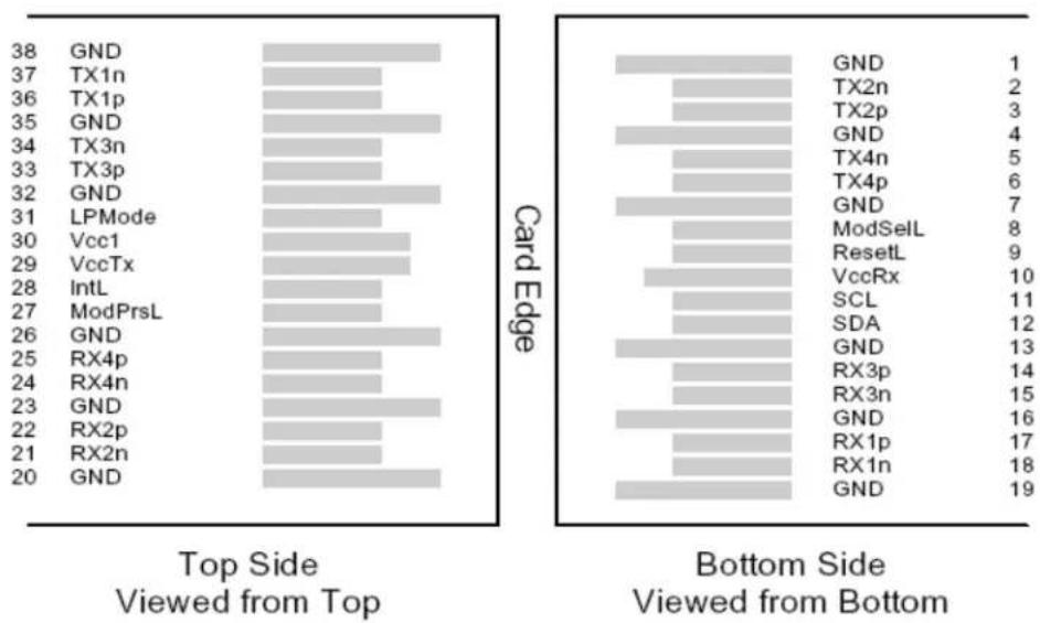
Figure 1-QSFP MSA-compliant 38-pin connector
| Pin | Symbol | Name/Description | Notes |
| 1 | GND | Ground | 1 |
| 2 | Tx2n | Transmitter Inverted Data Input | |
| 3 | Tx2p | Transmitter Non-Inverted Data Input | |
| 4 | GND | Ground | 1 |
| 5 | Tx4n | Transmitter Inverted Data Input | |
| 6 | Tx4p | Transmitter Non-Inverted Data Input | |
| 7 | GND | Ground | 1 |
| 8 | ModSelL | Module Select | |
| 9 | ResetL | Module Reset | |
| 10 | Vcc Rx | +3.3 V Power supply receiver | |
| 11 | SCL | 2-wire serial interface clock | |
| 12 | SDA | 2-wire serial interface data | |
| 13 | GND | Ground | 1 |
| 14 | Rx3p | Receiver Non-Inverted Data Output | |
| 15 | Rx3n | Receiver Inverted Data Output | |
| 16 | GND | Ground | 1 |
| 17 | Rx1p | Receiver Non-Inverted Data Output | |
| 18 | Rx1n | Receiver Inverted Data Output | |
| 19 | GND | Ground | 1 |
| 20 | GND | Ground | 1 |
| 21 | Rx2n | Receiver Inverted Data Output | |
| 22 | Rx2p | Receiver Non-Inverted Data Output | |
| 23 | GND | Ground | 1 |
| 24 | Rx4n | Receiver Inverted Data Output | |
| 25 | Rx4p | Receiver Non-Inverted Data Output | |
| 26 | GND | Ground | 1 |
| 27 | ModPrsL | Module Present | |
| 28 | IntL | Interrupt | |
| 29 | Vcc Tx | +3.3 V Power supply transmitter | |
| 30 | Vcc1 | +3.3 V Power Supply | |
| 31 | LPMode | Low Power Mode | |
| 32 | GND | Ground | 1 |
| 33 | Tx3p | Transmitter Non-Inverted Data Input | |
| 34 | Tx3n | Transmitter Inverted Data Input | |
| 35 | GND | Ground | 1 |
| 36 | Tx1p | Transmitter Non-Inverted Data Input | |
| 37 | Tx1n | Transmitter Inverted Data Input | |
| 38 | GND | Ground | 1 |
Notes
- Circuit ground is internally isolated from chassis ground.
b. SFP+ ends
| Pin | Symbol | Name/Description | Ref. |
| 1 | VEET | Transmitter Ground (Common with Receiver Ground) | 1 |
| 2 | TFAULT | Transmitter Fault. | 2 |
| 3 | TDIS | Transmitter Disable. Laser output disabled on high or open. | 3 |
| 4 | SDA | 2-wire Serial Interface Data Line | 4 |
| 5 | SCL | 2-wire Serial Interface Clock Line | 4 |
| 6 | MOD_ABS | Module Absent. Grounded within the module | 4 |
| 7 | RS0 | No connection required | |
| 8 | RX_LOS | Loss of Signal indication. Logic 0 indicates normal operation. | 5 |
| 9 | RS1 | No connection required | |
| 10 | VEER | Receiver Ground (Common with Transmitter Ground) | 1 |
| 11 | VEER | Receiver Ground (Common with Transmitter Ground) | 1 |
| 12 | RD- | Receiver Inverted DATA out. AC Coupled | |
| 13 | RD+ | Receiver Non-inverted DATA out. AC Coupled | |
| 14 | VEER | Receiver Ground (Common with Transmitter Ground) | 1 |
| 15 | VCCR | Receiver Power Supply | |
| 16 | VCCT | Transmitter Power Supply | |
| 17 | VEET | Transmitter Ground (Common with Receiver Ground) | 1 |
| 18 | TD+ | Transmitter Non-Inverted DATA in. AC Coupled. | |
| 19 | TD- | Transmitter Inverted DATA in. AC Coupled. | |
| 20 | VEET | Transmitter Ground (Common with Receiver Ground) | 1 |
Notes:
- Circuit ground is internally isolated from chassis ground.
- T_FAULT is an open collector/drain output, which is pulled up with a 4.7k - 10k Ohms resistor on the host board, but is grounded inside the SFP+ cable plug.
- Laser output disabled on TDIS > 2.0V or open, enabled on TDIS < 0.8V .
- Should be pulled up with 4.7k -10k on host board to a voltage between 2.0V and 3.6V. MOD ABS pulls line low to indicate module is plugged in.
- LOS is open collector output. Should be pulled up with 4.7k - 10k on host board to a voltage between 2.0V and 3.6V. Logic 0 indicates normal operation; logic 1 indicates loss of signal.
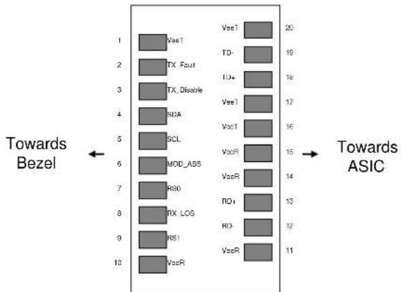
Figure 2. Diagram of Host Board Connector Block Pin Numbers and Names on the SFP+ ends.
II. General Product Characteristics
| Parameter | Value | Unit | Notes |
| Module Form Factor | QSFP+ and SFP+ | ||
| Number of Lanes | 4 Tx and 4 Rx | ||
| Maximum Aggregate Data Rate | 42.0 | Gb/s | |
| Maximum Data Rate per Lane | 10.3125 | Gb/s | |
| Standard Cable Lengths | 1, 2, 3, 5, 7, 10, 15, 20, 30 | meters | Other lengths may be available upon request |
| Protocols Supported | 10G Ethernet | ||
| Electrical Interface and Pin-out | 38-pin edge connector (QSFP+) and 20-pin edge connector (SFP+) | Pin-out as defined by the QSFP+ and SFP+ MSAs | |
| Standard Optical Cable Type | Multimode fiber cable assembly, plenum-rated | OFNP | |
| Maximum Power Consumption per End | 1.3 (QSFP+) and 1 (SFP+) | Watts | Varies with output voltage swing and pre-emphasis settings |
| Management Interface | Serial, I2C-based, 400 kHz maximum frequency | As defined by the QSFP MSA |
| Data Rate Specifications | Symbol | Min | Typ | Max | Units | Ref. |
| Bit Rate per Lane | BR | 1000 | 103125 | Mb/sec | ||
| Bit Error Ratio | BER | \( 10^{-12} \) | 1 |
Notes:
1. Tested with a PRBS 2 ^31 -1 test pattern.
III. Absolute Maximum Ratings
| Parameter | Symbol | Min | Typ | Max | Unit | Ref. |
| Maximum Supply Voltage | Vcc1, VccTx, VccRx | -0.5 | 3.6 | V | ||
| Storage Temperature | TS | -10 | 75 | °C | ||
| Case Operating Temperature | TOP | 0 | 70 | °C | ||
| Relative Humidity | RH | 0 | 85 | % | 1 |
Notes:
- Non-condensing.
IV. Electrical Characteristics (T OP = 0 to 70^ , V_CC = 3.3 ± 5% Volts)
| Parameter | Symbol | Min | Typ | Max | Unit | Ref. |
| Supply Voltage | Vcc1, VccTx, VccRx | 3.15 | 3.45 | V | ||
| Supply Current | Icc | 350 (QSFP)250 (SFP+) | mA | |||
| Link Turn-On Time | ||||||
| Transmit Turn-On Time | 2000 | ms | 1 | |||
| Transmitter (per Lane) | ||||||
| Differential data input swing | Vin,pp | 180 | 1200 (QSFP)700 (SFP+) | mVpp | 2 | |
| Differential input threshold | 50 | mV | ||||
| Receiver (per Lane) | ||||||
| Differential data output swing | Vout,pp | 0 | 850 | mVpp | 3.4 | |
| Power Supply Ripple Tolerance | PSR | 50 | mVpp | |||
Notes:
- From power-on and end of any fault conditions.
- AC coupled internally. See Figure 2 for input eye mask requirements. Self-biasing 100 differential input.
- AC coupled with 100 differential output impedance. See Figure 3 for output eye mask.
- Settable in 4 discrete steps. See Figure 5 for Vo settings
V. High-Speed Electrical Characteristics per Lane
(TOP = 0 to 70^ C, VCC = 3.3 ± 5 % . Volts)
| Parameter-Inputs | Symbol | Conditions | Min | Typ | Max | Units | Ref. |
| Reference Differential Input Impedance | Zd | 100 | Ω | ||||
| Termination Mismatch | ΔZM | 5 | % | 1 | |||
| Input AC Common Mode Voltage | 25 | mV (RMS) | |||||
| Differential Input Return Loss | SDD11 | 0.01-4.1 GHz | dB | 2 | |||
| 4.1 - 11.1 GHz | dB | 3 | |||||
| Differential to Common Mode Loss | SCD11 | 0.01-11.1 GHz | -10 | dB | |||
| Eye Mask Coordinates: | X1, X2 | 0.29, 0.5 | UI | 4 | |||
| Y1, Y2 | 150, 425 | mV | |||||
| Jitter Tolerance (Total) | TJ | 0.40 | UI | ||||
| Jitter Tolerance (Deterministic) | DJ | 0.15 | UI |
Notes:
1. See SFF-8431 Rev 3.2 (SFP+) section D.15 Termination Mismatch for definition & test recommendations
2. Reflection coefficient given by equation SDD11(dB) < -12 + 2^*SQRT(f) with f in GHz.
3. Reflection coefficient given by equation SDD11(dB) < - 6.3 + 13Log10(f / 5.5) , with f in GHz.
4. Hit ratio 5 × 10^-5 . See Figure 3 for transmitter input eye mask definitions.
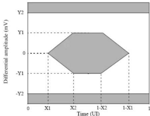
Figure 3 - Transmitter Input Differential Signal Mask
| Parameter -Outputs | Symbol | Conditions | Min | Typ | Max | Units | Ref. |
| Reference Differential Output Impedance | Zd | 100 | Ω | ||||
| Termination Mismatch | ΔZM | 5 | % | ||||
| Output AC Common Mode Voltage | 15 | mVRMS | |||||
| Output Rise and Fall time (20% to 80%) | tRH, tFH | 24 | ps | ||||
| Differential Output Return Loss | SDD22 | 0.01-4.1 GHz | dB | 1 | |||
| 4.1 - 11.1 GHz | dB | 2 | |||||
| Common Mode Output Return Loss | SCC22 | 0.01-2.5 GHz | dB | 3 | |||
| 2.5-11.1 GHz | -3 | dB | |||||
| Eye Mask Coordinates: | X1, X2 | 0.29, 0.5 | UI | 4 | |||
| Y1, Y2 | 150, 425 | mV | |||||
| Deterministic Jitter | DJOUT | 0.38 | UI | 1 | |||
| Total Jitter | TJOUT | 0.64 | UI | 1 |
Notes:
1. Reflection coefficient given by equation SDD22(dB) < -12 + 2^SQRT(f) with f in GHz. See Figure 5.
2. Reflection coefficient given by equation SDD22(dB) < -6.3 + 13Log10(f / 5.5) , with f in GHz. See Figure 5.
3. Reflection coefficient given by equation SCC22(dB) < - 7 + 1.6^f, with f in GHz.
4. Hit ratio 5 × 10^-5 . See Figure 4 for receiver output eye mask definitions.
5. When transmitter input jitter specs are met
| Other Informational Specifications (not tested) | Symbol | Min | Typ | Max | Units | Ref. |
| Max Bit Rate NRZ | B | 12.5 | Gb/s | |||
| Low Frequency 3dB Cutoff | fc | 175 | kHz | |||
| Ch / Ch crosstalk | -26 | dB | ||||
| Output Pre-emphasis settings (user selectable) | PE | 0 | mV | |||
| 125 | mV | |||||
| 175 | mV | |||||
| 325 | mV | |||||
| Pre-Emphasis pulse width | 60 | 90 | ps | |||
| Channel Latency | TBD | |||||
| Digital clock to data delay | 25 | ns | ||||
| Digital output rise/fall times | 5 | ns | ||||
| Digital input / output Cap | 1 | pF | ||||
| Digital input logic High | 2 | V | ||||
| Digital input logic Low | 1 | V | ||||
| ESD Signal pads | 500 | V | HBM | |||
| ESD (other pads) | 2 | kV | HBM |
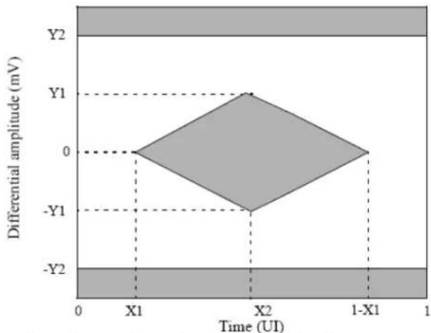
Figure 4 - Receiver Output Differential Signal Mask
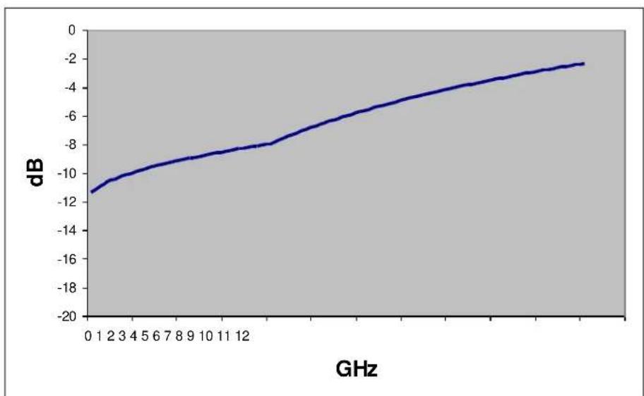
Figure 5 - Maximum Transmitter Input and Receiver Output Differential Return Loss
| Power (mW) | Pre-Emphasis into 100ohms (mV) | ||||
| 0 | 125 | 175 | 325 | ||
| U(mV) | 0 | 599 | |||
| 317 | 751 | 935 | 971 | 1075 | |
| VoA | 422 | 787 | 971 | 1007 | 1111 |
| 739 | 883 | 1055 | 1103 | 1190 | |
Figure 6 - Power Dissipation (mW, maximum) vs. Rx Output Conditions
VI. Memory Map and Control Registers
Compatible with SFF-8436. More details to be provided in a future revision of this document.
VII. Environmental Specifications
Finisar Quadwire active optical cables have an operating temperature range from 0^ to +70^ case temperature.
| Environmental Specifications | Symbol | Min | Typ | Max | Units | Ref. |
| Case Operating Temperature | Top | 0 | 70 | °C | ||
| Storage Temperature | Tsto | -10 | 75 | °C |
VIII. Regulatory Compliance
Finisar Quadwire active optical cables are RoHS-6 Compliant. Copies of certificates are available at Finisar Corporation upon request.
Quadwire active optical cables are Class 1 laser eye safety compliant per IEC 60825-1.
Standard fiber cable type is OFNP plenum rated, round construction. Other cable types may be supported upon request.
IX. Mechanical Specifications
The Quadwire mechanical specifications are based on QSFP+ and SFP+ transceiver module specifications, substituting the optical connectors with a cable connecting both ends.
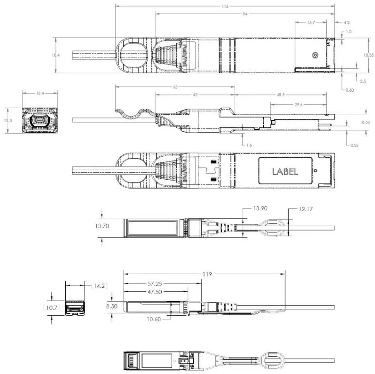
Figure 5 -Mechanical drawing of Quadwire QSFP+ and SFP+ ends
| Quadwire length | Breakout point (measured from QSFP) | Breakout point (measured from SFP+) |
| 1m | 33cm | 67cm |
| 2m | 67cm | 1.33m |
| 3m | 1m | 2m |
| 5m | 2m | 3m |
| 7m | 4m | 3m |
| 10m | 7m | 3m |
| 15m | 12m | 3m |
| 20m | 17m | 3m |
| 30m | 27m | 3m |
| Cable Mechanical Specifications | Min | Typical | Max | Units |
| Minimum bend radius | 60 | mm | ||
| Minimum bend radius within 100 mm of a module end | 105 | mm | ||
| Diameter of common (non-broken-out) cable jacket | 3.0 | 3.3 | 3.6 | mm |
| Diameter of broken-out cable jacket | 1.8 | 2.0 | 2.2 | mm |
| Insertion, Extraction and Retention Forces | Min | Max | Units | Notes |
| Cable Proof (Tensile) Test (0°) | 44.0 | Newtons | ||
| Cable Proof (Tensile) Test (90°) | 33.0 | Newtons | ||
| Impact Test | 8 | Cycles | 1.5m drop | |
| Flex Test | 8.9 | Newtons | ||
| Twist Test | 13.0 | Newtons | ||
| Module retention | 90 | N/A | Newtons | No damage below 90N |
| Host Connector Retention | 180 | N/A | Newtons | No damage below 180N |
Finisar Sunnyvale,CA 94089
FCBN510QE2Cxx
QSFP-40G-SR4 XX M
MADE IN CHINA
Class 1 21CFR1040.10 LN#506/2007
S/N: WWWWWWW

Finisar Sunnyvale,CA 94089

Figure 6 - Quadwire product labels: QSFP end (top) and SFP+ ends (bottom)
X. References
- SFF-8436 - Specification for QSFP+ Copper and Optical Transceiver, Rev 4.8, October 2013.
- "Specifications for Enhanced 8.5 and 10 Gigabit Small Form Factor Pluggable Module 'SFP+, SFF Document Number SFF-8431, Revision 4.1.
- Directive 2011/65/EC of the European Council Parliament and of the Council, "on the restriction of the use of certain hazardous substances in electrical and electronic equipment," June 8, 2011 which supercedes the previous RoHS Directive 2002/95/EC.
- "Application Note AN-2038: Finisar Implementation of RoHS Compliant Transceivers", Finisar Corporation, January 21, 2005.
- "Application Note AN-2079: QSFP Module EEPROM Mapping", Rev. G, Finisar Corporation, May, 2013.
XI. For More Information
Finisar Corporation
1389 Moffett Park Drive
Sunnyvale, CA 94089-1133
Tel. 1-408-548-1000
Fax 1-408-541-6138
sales@finisar.com
www.finisar.com