
AX34PRO - Carte mère AOPEN - Notice d'utilisation et mode d'emploi gratuit
Retrouvez gratuitement la notice de l'appareil AX34PRO AOPEN au format PDF.

| Type de produit | Carte mère ATX |
| Marque | AOPEN |
| Modèle | AX34PRO |
| Socket CPU | Socket 370 |
| CPU supportés | Intel Celeron, Pentium III (Coppermine, Tualatin) |
| Chipset | VIA 694X / VT82C686A |
| Format de la carte | ATX (305 x 244 mm) |
| Mémoire vive | 3 x DIMM 168 broches, PC133 SDRAM, max 1.5 Go |
| Slots d'extension | 1 x AGP 4X, 5 x PCI, 1 x AMR |
| Stockage | 2 x IDE (ATA/66/100), 1 x FDD |
| Ports USB | 4 x USB 1.1 (2 arrière, 2 via connecteur interne) |
| Audio intégré | AC97 (CODEC AD1881) |
| Connecteurs arrière | PS/2 clavier/souris, 2 x COM, LPT, 2 x USB, audio (Line-in, Line-out, Mic), Game/MIDI |
| BIOS | Award BIOS avec support Die-Hard (protection anti-virus matérielle), langues multiples |
| Alimentation | ATX 20 broches, support Wake-on-Modem/LAN/RTC |
| Fonctions spéciales | Jumperless CPU, réglage tension CPU (1.3-3.5V), overclocking FSB jusqu'à 150 MHz, surveillance matérielle, fusible réarmable, condensateurs 2200 µF Low ESR |
| Gestion d'énergie | ACPI S1/S3 (Suspend to RAM), Suspend to Disk, réveil sur modem/LAN/PCI/RTC |
| Température de fonctionnement | 0°C à 50°C |
| Entretien et nettoyage | Dépoussiérer avec air comprimé, éviter l'humidité |
| Sécurité | Protection contre les surintensités, BIOS anti-virus, mot de passe BIOS |
| Pièces détachées et réparabilité | Fusible réarmable, batterie CMOS remplaçable, support technique AOpen |
FOIRE AUX QUESTIONS - AX34PRO AOPEN
Questions des utilisateurs sur AX34PRO AOPEN
0 question sur cet appareil. Repondez a celles que vous connaissez ou posez la votre.
Poser une nouvelle question sur cet appareil
Téléchargez la notice de votre Carte mère au format PDF gratuitement ! Retrouvez votre notice AX34PRO - AOPEN et reprennez votre appareil électronique en main. Sur cette page sont publiés tous les documents nécessaires à l'utilisation de votre appareil AX34PRO de la marque AOPEN.
MODE D'EMPLOI AX34PRO AOPEN
AX34 Pro
Online Manual
DOC. NO.: AX34P-OL-E0004B
What's in this manual
AX34 Pro 1
What's in this manual. 2
Before You Start 10
Quick Installation Procedure 11
Motherboard Map 12
Block Diagram 13
Hardware 14
JP14 Clear CMOS 15
CPU Socket 16
CPU and Housing Fan Connector 17
CPU Jumper-less Design 18
JP29/JP23 FSB/PCI Clock Ratio 22
JP33/JP32 Select CPU Type 24
DIMM Socket 25
RAM Power LED. 27
AX34 Pro
Online Manual
Front Panel Connector 28
ATX Power Connector. 30
AC Power Auto Recovery 31
IDE and Floppy Connector 32
IrDA Connector 35
WOM (Zero Voltage Wake on Modem) 36
WOL (Wake on LAN) 39
4X AGP (Accelerated Graphic Port) 41
AMR (Audio/Modem Riser) 42
PC99 Color Coded Back Panel 43
Support 4 USB Ports. 44
JP12 Enable/Disable Onboard Sound 45
CD Audio Connector 46
Modem Audio Connector 47
Video_Audio_IN Connector 48
Battery-less and Long Life Design 49
Over-current Protection 50
Hardware Monitoring. 52
Resettable Fuse. 53
JP30 Die-Hard BIOS (100% Virus Protection) 54
Year 2000 (Y2K) 56
2200uF Low ESR Capacitor 58
Layout (Frequency Isolation Wall) 60
24K Gold Heatsink 61
Driver and Utility 62
Autorun Menu from Bonus CD Disc 63
Installing Windows 95 64
Installing Windows 98 65
Installing Windows 98 SE & Windows2000 66
Installing VIA 4 in 1 Driver 67
68
69
ACPI Suspend to Hard Drive 70
ACPI Suspend to RAM (STR) 77
AWARD BIOS 79
EnterBIOS Setup 80
Change Language 81
Standard CMOS Setup 82
BIOS Features Setup 88
Chipset Features Setup 99
Power Management Setup. 108
PNP/PCI Configuration Setup 118
Load Setup Defaults 126
Load Turbo Defaults 127
Integrated Peripherals 128
Password Setting 140
IDE HDD Auto Detection 141
Save & Exit Setup 143
AX34 Pro
Online Manual
Load EEPROM Default 144
Save EEPROM Default. 144
Exit without Saving. 144
NCR SCSI BIOS and Drivers 144
BIOS Upgrade 145
Overclocking 146
VGA and HDD 148
Glossary 149
AC97 149
ACPI (Advanced Configuration & Power Interface) 149
AGP (Accelerated Graphic Port) 150
AMR (Audio/Modem Riser) 150
AOpen Bonus Pack CD 150
APM 150
ATA/66 151
ATA/100 151
AX34 Pro
Online Manual
BIOS (Basic Input/Output System) 151
Bus Master IDE (DMA mode) 152
CODEC (Coding and Decoding) 152
DIMM (Dual In Line Memory Module) 152
ECC (Error Checking and Correction) 152
EDO (Extended Data Output) Memory 153
EEPROM (Electronic Erasable Programmable ROM) 153
EPROM (Erasable Programmable ROM) 153
FCC DoC (Declaration of Conformity) 153
FC-PGA 154
Flash ROM 154
FSB (Front Side Bus) Clock 154
I2C Bus. 154
P1394 155
Parity Bit 155
PBSRAM (Pipelined Burst SRAM) 155
AX34 Pro
Online Manual
PC100 DIMM 155
PC133 DIMM 156
PDF Format 156
PnP (Plug and Play) 156
POST (Power-On Self Test) 156
RDRAM (Rambus DRAM) 157
RIMM 157
SDRAM (Synchronous DRAM) 157
SIMM (Single In Line Memory Module) 157
SMBus (System Management Bus) 158
SPD (Serial Presence Detect) 158
Ultra DMA/33 158
USB (Universal Serial Bus) 159
ZIP file 159
Troubleshooting 160
Technical Support. 164
AX34 Pro
Online Manual
Part Number and Serial Number 166
Model name and BIOS version 167
Before You Start

This Online Manual is in PDF format, we recommend using Adobe Acrobat Reader 4.0 for online viewing, it is included in Bonus CD disc or you can get free download from Adobe web site.
Although this Online Manual is optimized for screen viewing, it is still capable for hardcopy printing, you can print it by A4 paper size and set 2 pages per A4 sheet on your printer. To do so, choose File > Page Setup and follow the instruction of your printer driver.
Thanks for the help of saving our earth.
Quick Installation Procedure
This page gives you a quick procedure on how to install your system. Follow each step accordingly.
1 Installing CPU and Fan
Installing System Memory (DIMM)
3 Connecting Front Panel Cable
4 Connecting IDE and Floppy Cable
3 Connecting ATX Power Cable
6 Connecting Back Panel Cable
7 Power-on and Load BIOS Setup Default
Setting CPU Frequency
Reboot
10 Installing Operating System (such as Windows 98)
11 Installing Driver and Utility
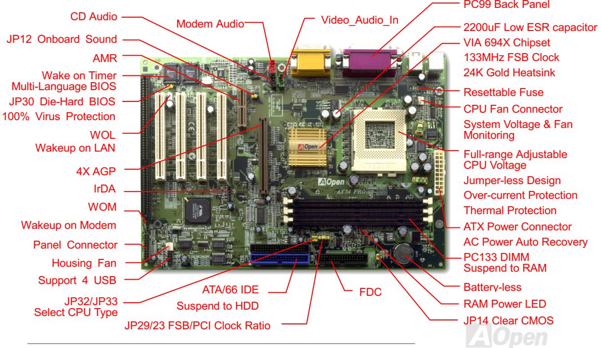
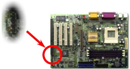
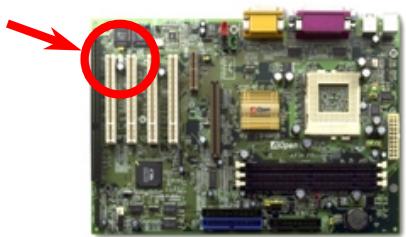
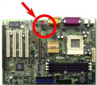
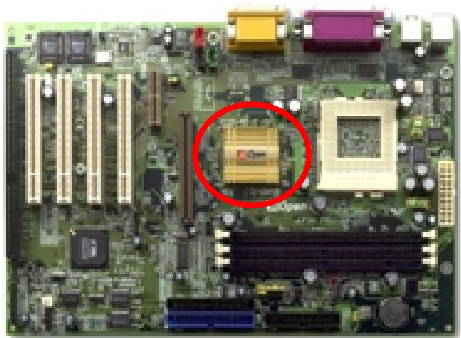
Motherboard Map
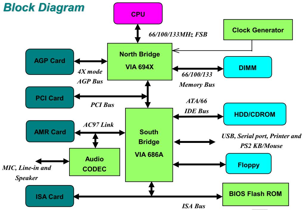
Block Diagram
Hardware
This chapter describes jumpers, connectors and hardware devices of this motherboard.

Note: Electrostatic discharge (ESD) can damage your processor, disk drives, expansion boards, and other components. Always observe the following precautions before you install a system component.
- Do not remove a component from its protective packaging until you are ready to install it.
2.Wear a wrist ground strap and attach it to a metal part of the system unit before handling a component. If a wrist strap is not available, maintain contact with the system unit throughout any procedure requiring ESD protection.
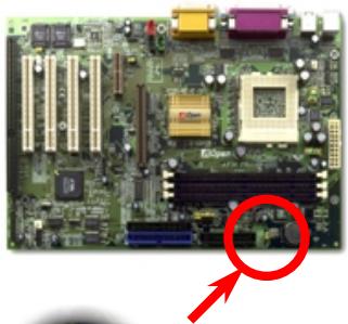
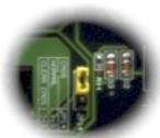
JP14 Clear CMOS

Normal Operation (default)

Clear CMOS
You can clear CMOS to restore system default setting. To clear the CMOS, follow the procedure below.
- Turn off the system and unplug the AC power.
- Remove ATX power cable from connector PWR2.
- Locate JP14 and short pins 2-3 for a few seconds.
- Return JP14 to its normal setting by shorting pins 1-2.
- Connect ATX power cable back to connector PWR2.

Tip: When should I Clear CMOS?
- Boot fail because of overclocking...
- Forget password...
- Troubleshooting....
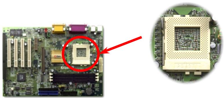
CPU Socket
This motherboard supports Celeron, and Pentium III Socket370 CPU. Be careful of CPU orientation when you plug it into CPU socket.
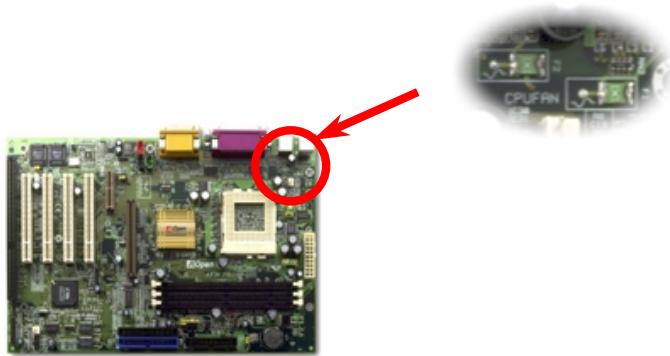
CPU and Housing Fan Connector
Plug in the CPU fan cable to the 3-pin CPUFAN connector. If you have other housing fan, you can also plug it on FAN connector.

GND
+12V
SENSOR

Note: Some CPU fans do not have sensor pin, so that cannot support fan monitoring.
CPU Jumper-less Design
CPU VID signal and SMbus clock generator provide CPU voltage auto-detection and allows the user to set the CPU frequency through the BIOS setup, therefore no jumpers or switches are used. The correct CPU information is saved into the EEPROM. With these technologies, the disadvantages of the Pentium based jumper-less designs are eliminated. There will be no worry of wrong CPU voltage detection and no need to re-open the housing in case of CMOS battery loss.
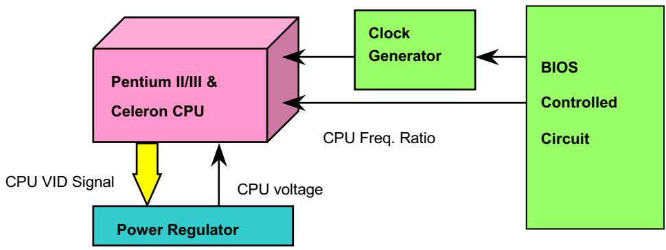
(Automatically generates CPU voltage)
Full-range Adjustable CPU Core Voltage
This function is dedicated to overclockers, AOpen works together with Fairchild to develop a special chip FM3540 which supports Adjustable CPU Core Voltage from 1.3V to 3.5 by 0.05 or 0.1V stepping. But this motherboard can also automatically detect CPU VID signal and generates proper CPU core voltage.
BIOS Setup > Chipset Features Setup > CPU Voltage Setting

Warning: High CPU core voltage may be able to increase CPU speed for overclocking, but you may damage the CPU or reduce the CPU lifecycle.
Setting CPU Frequency
This motherboard is CPU jumper-less design, you can set CPU frequency through the BIOS setup, no jumpers or switches are needed.
BIOS Setup > Chipset Features Setup > CPU Clock Frequency
BIOS Setup > Chipset Features Setup > CPU Clock Ratio
| CPU Ratio | 1.5x, 2x, 2.5x, 3x, 3.5x, 4x, 4.5x, 5x, 5.5x, 6x, 6.5x, 7x, 7.5x, and 8x |
| CPU FSB | 66.8, 75, 83.3, 100, 103, 105, 110, 112, 115, 120, 124, 133, 140, and 150 MHz. |
Core Frequency = CPU FSB Clock * CPU Ratio
| CPU Type | FSB Clock | Ratio |
| Pentium!!! 500E (Socket370) | 100MHZ | 5x |
| Pentium!!! 550E (Socket370) | 100MHZ | 5.5x |
| Pentium!!! 600E (Socket370) | 100MHZ | 6x |
| Pentium!!! 667EB (Socket370) | 133MHZ | 5x |
| Pentium!!! 700E (Socket370) | 100MHZ | 7x |
| Pentium!!! 733EB (Socket370) | 133MHZ | 5.5x |
| Pentium!!! 866EB (Socket370) | 133MHZ | 6x |
| Pentium!!! 500E (Socket370) | 100MHZ | 5x |
| Pentium!!! 500E (Socket370) | 100MHZ | 5x |
| Pentium!!! 550E (Socket370) | 100MHZ | 5.5x |
| Pentium!!! 600E (Socket370) | 100MHZ | 6x |
| Pentium!!! 667EB (Socket37O) | 133MHZ | 5x |
| Pentium!!! 700E (Socket370) | 100MHZ | 7x |
| Pentium!!! 733EB (Socket370) | 133MHZ | 5.5x |
| Pentium!!! 866EB (Socket370) | 133MHZ | 6x |
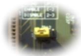
JP29/JP23 FSB/PCI Clock Ratio
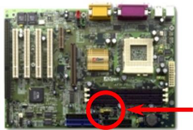
This jumper is used to specify the relationship of PCI and FSB clock. Generally speaking, if you are not overclockers, we recommend to set at the default setting.

JP29
12

JP23
12

Auto
(default)
JP29
12

JP23
12

4X (133~150MHz)
JP29
12
JP23
12

。
(100~124MHz)
JP29
12

JP23
12

2X
(66~83MHz)
PCI Clock = CPU FSB Clock / Clock Ratio
AGP Clock = PCI Clock x 2
| Clock Ratio | CPU (Host) | PCI | AGP | Memory |
| 2X | 66 | 33 | 66 | PCI x2 or x3 |
| 3X | 100 | 33 | 66 | PCI x2 or x3 or x4 |
| 3X, overclocking | 112 | 37.3 | 74.6 | PCI x2 or x3 or x4 |
| 4X | 133 | 33 | 66 | PCI x3 or x4 |
| 4X, overclocking | 155 | 38.75 | 77.5 | PCI x3 or x4 |
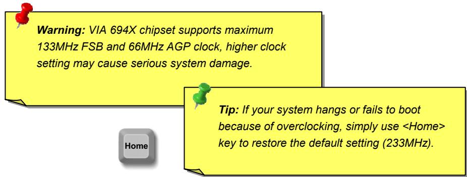
Warning: VIA 694X chipset supports maximum 133MHz FSB and 66MHz AGP clock, higher clock setting may cause serious system damage.
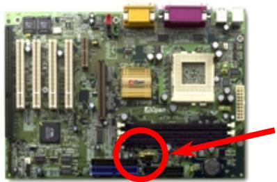
JP33/JP32 Select CPU Type
This jumper is used to select various CPU type.

| CPU Type | JP33 | JP32 |
| Coppermine | 1-2 | 1-2 |
| Celeron | 2-3 | 1-2 |
JP33/JP32

Coppermine
JP33/JP32

Celeron
JP33/JP32

Joshua
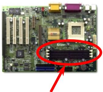
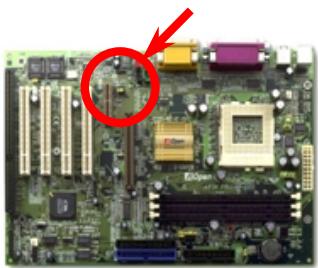
DIMM Socket
This motherboard has three 168-pin DIMM sockets that allow you to install PC133 memory up to 1.5GB. Only SDRAM is supported.
Pin 1
DIMM1
DIMM2
DIMM3

Tip: The driving capability of new generation chipset is limited due to the lack of a memory buffer (to improve performance). This makes DRAM chip count an important factor to take into consideration when you install DIMMs. Unfortunately, there is no way that the BIOS can identify the correct chip count, you need to calculate the chip count by yourself. The simple rule is: By visual inspection, use only DIMMs which are less than 16 chips.
DIMM can be single side or double side, it has 64 bit data and 2 or 4 clock signals. We strongly recommend choosing 4-clock SDRAM for its reliability

Tip: To identify 2-clock and 4-clock DIMM, you may check if there are traces connected to the golden finger pins 79 and 163 of the SDRAM. If there are traces, the SDRAM is probably 4-clock; otherwise, it is 2-clock.

Tip: To identify single-side or double-side DIMM, check golden finger pin 114 and pin 129. If there are traces connected to pin 114 and pin 129, the DIMM is probably double-side; otherwise, it is single-side.
RAM Power LED
This LED indicates there is power applies to memory. It is useful to check RAM power during Suspend to RAM. Do not unplug memory module when this LED is On.

Front Panel Connector
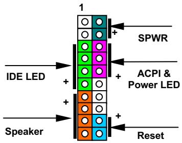
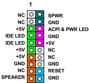
Attach the power LED, keylock, speaker, and reset switch connectors to the corresponding pins. If you enable Power Management Setup > Suspend Mode in BIOS Setup, the ACPI & Power LED will keep flashing while the system is in suspend mode.
| Suspend Type | ACPI LED |
| Power on Suspend (S1) | Flashing for every second |
| Suspend to RAM (S3) | Flashing for every 4 seconds |
Locate the power switch cable from your ATX housing. It is 2-pin female connector from the housing front panel. Plug this connector to the soft-power switch connector marked SPWR.
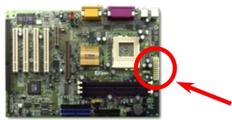
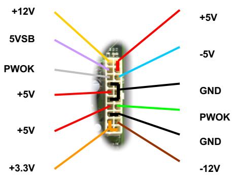
ATX Power Connector
The ATX power supply uses 20-pin connector shown below. Make sure you plug in the right direction.
AC Power Auto Recovery
A traditional ATX system should remain at power off stage when AC power resumes from power failure. This design is inconvenient for a network server or workstation, without an UPS, that needs to keep power-on. This motherboard implements an AC Power Auto Recovery function to solve this problem. If BIOS Setup > Power management > AC PWR Auto Recovery is set to "On" the system will automatically power-on after AC power resumes.
IDE and Floppy Connector
Connect 34-pin floppy cable and 40-pin IDE cable to floppy connector FDC and IDE connector The blue connector is IDE1 for clear identification. Be careful of the pin1 orientation. Wrong orientation may cause system damage.
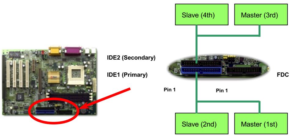
IDE1 is also known as the primary channel and IDE2 as the secondary channel. Each channel supports two IDE devices that make a total of four devices. In order to work together, the two devices on each channel must be set differently to master and slave mode. Either one can be the hard disk or the CDROM. The setting as master or slave mode depends on the jumper on your IDE device, so please refer to your hard disk and CDROM manual accordingly.
This motherboard supports ATA/66 IDE. Following table lists the transfer rate of IDE PIO and DMA modes. The IDE bus is 16-bit, which means every transfer is two bytes.
| Mode | Clock Period | Clock Count | Cycle Time | Data Transfer Rate |
| PIO mode 0 | 30ns | 20 | 600ns | (1/600ns) x 2byte = 3.3MB/s |
| PIO mode 1 | 30ns | 13 | 383ns | (1/383ns) x 2byte = 5.2MB/s |
| PIO mode 2 | 30ns | 8 | 240ns | (1/240ns) x 2byte = 8.3MB/s |
| PIO mode 3 | 30ns | 6 | 180ns | (1/180ns) x 2byte = 11.1MB/s |
| PIO mode 4 | 30ns | 4 | 120ns | (1/120ns) x 2byte = 16.6MB/s |
| DMA mode 0 | 30ns | 16 | 480ns | (1/480ns) x 2byte = 4.16MB/s |
| DMA mode 1 | 30ns | 5 | 150ns | (1/150ns) x 2byte = 13.3MB/s |
| DMA mode 2 | 30ns | 4 | 120ns | (1/120ns) x 2byte = 16.6MB/s |
| UDMA/33 | 30ns | 4 | 120ns | (1/120ns) x 2byte x2 = 33MB/s |
| UDMA/66 | 30ns | 2 | 60ns | (1/60ns) x 2byte x2 = 66MB/s |
| UDMA/100 | 20ns | 2 | 40ns | (1/40ns) x 2byte x2 = 100MB/s |

Tip: To achieve the best performance of Ultra DMA/66 hard disks, a special 80-wires IDE cable for Ultra DMA/66 is required..
IrDA Connector
The IrDA connector can be configured to support wireless infrared module, with this module and application software such as Laplink or Windows 95 Direct Cable Connection, the user can transfer files to or from laptops, notebooks, PDA devices and printers. This connector supports HPSIR (115.2Kbps, 2 meters) and ASK-IR (56Kbps).
Install the infrared module onto the IrDA connector and enable the infrared function from BIOS Setup, UART 2 Mode, make sure to have the correct orientation when you plug in the IrDA connector.
Pin 1
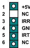
+5V
NC
。
IRRX
O
GND
O
IRTX
NC
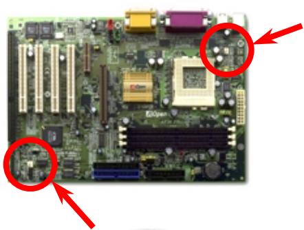
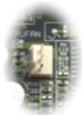
WOM (Zero Voltage Wake on Modem)
This motherboard implements special circuit to support Wake On Modem, both Internal modem card and external box modem are supported. Since Internal modem card consumes no power when system power is off, it is recommended to use an internal modem. To use internal modem, connect 4-pin cable from RING connector of modem card to the WOM connector on the motherboard.
1

+5V Standby
NC
RING
GND
Pin 1
WOM by External BOX Modem
Traditional Green PC suspend mode does not really turn off the system power supply, it uses external box modem to trigger MB COM port and resume back to active.
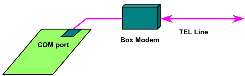
Motherboard
WOM by Internal Modem Card
With the help of the ATX soft power On/Off, it is possible to have a system totally power off, and wakeup to automatically answer a phone call as an answering machine or to send/receive a fax. You may identify whether or not your system is in true power off mode by checking to see if the fan of your power supply is off. Both an external box modem and an internal modem card can be used to support Modem Wake Up, but if you use an external modem, you have to leave your box modem on.

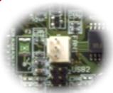
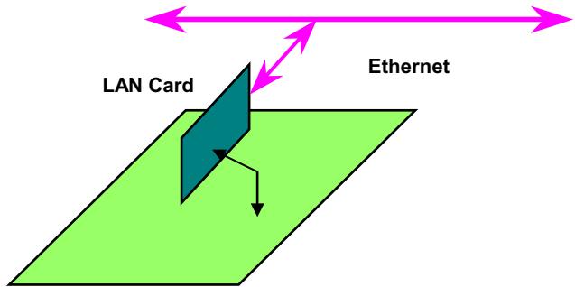
WOL (Wake on LAN)
This feature is very similar as Wake On Modem, but it goes through local area network. To use Wake On LAN function, you must have a network card with chipset that supports this feature, and connect a cable from LAN card to motherboard WOL connector. The system identification information (probably IP address) is stored on network card and because there is a lot of traffic on the Ethernet, you need to install a network management software, such as ADM, for the checking of how to wake up the system. Note that, at least 600mA ATX standby current is required to support the LAN card for this function.

+5V Standby
GND
LID

Pin 1
Motherboard
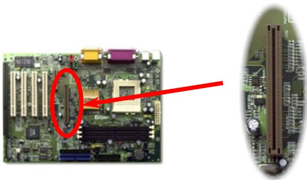
4X AGP (Accelerated Graphic Port)
This motherboard supports 4X AGP. AGP is a bus interface designed for high-performance 3D graphic and supports only memory read/write operation. One motherboard can only have one AGP slot. 2X AGP uses both rising and falling edge of the 66MHz clock, the data transfer rate is 66MHz x 4 bytes x 2 = 528MB/s. 4X AGP is still using 66MHz AGP clock but the it has 4 data transfers within one 66MHz clock cycle, so that the data transfer rate is 66MHz x 4 bytes x 4 = 1056MB/s.
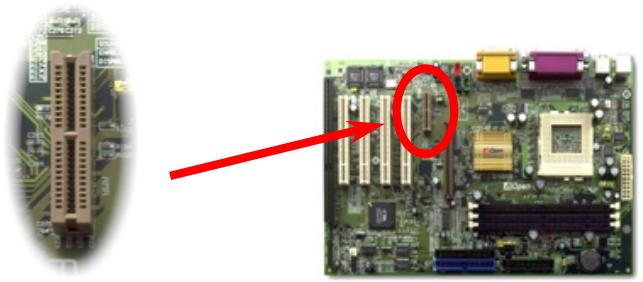
AMR (Audio/Modem Riser)
AMR is a riser card that supports sound or modem function. Because CPU computing power is getting stronger, the digital processing job can be implemented in main chipset and share CPU power. The analog conversion (CODEC) circuit requires a different and separate circuit design, it is put on AMR card. This motherboard implements sound CODEC on board (can be disabled by JP12), but reserve AMR slot for the option of modem function. Note that you can still use PCI modem card.
PC99 Color Coded Back Panel
The onboard I/O devices are PS/2 Keyboard, PS/2 Mouse, serial ports COM1 and COM2, Printer, four USB, AC97 sound and Game port. The view angle of drawing shown here is from the back panel of the housing.
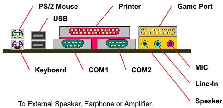
Speaker: To External Speaker, Earphone or Amplifier.
Line-In: From signal source such as CD/Tape player.
MIC: From Microphone
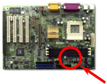
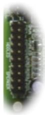
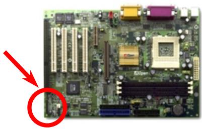
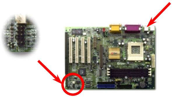
Support 4 USB Ports
This motherboard supports four USB ports. Two of them are on back panel connector, the other two are on the left-bottom area of this motherboard. With proper cable, you can connect them to front panel.

Pin 1
JP12 Enable/Disable Onboard Sound
This motherboard has AC97 sound onboard. JP12 is used to enable or disable onboard AD1881 CODEC chip. If you select Disable, you can use your preferred AMR sound card.
123

Enable
123

Disable
CD Audio Connector
This black connector is used to connect CD Audio cable from CDROM or DVD drive to onboard sound.
Pin 1
CD-IN
L
GND
GND
R
Modem Audio Connector
This connector is used to connect Mono In/Mic Out cable from internal modem card to onboard sound circuit. The pin 1-2 is Mono In, and the pin 3-4 is Mic Out. Please note that there is no standard for this kind of connector yet, only some internal modem cards implement this connector.
Pin 1
MODEM-CN

1
2
3
4
Mono In (to modem)
GND
GND
Mic Out (from Modem)
Video_Audio_IN Connector
This green connector is used to connect MPEG Audio cable from MPEG card to onboard sound.
Pin 1
VIDEO=AUDIO_IN

1 L
2 GND
3 GND
4 R
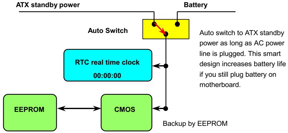
Battery-less and Long Life Design
This Motherboard implements EEPROM and a special circuit that allows you to save your current CPU and CMOS Setup configurations without the need of a battery. The RTC (real time clock) can also keep running as long as the power cord is plugged. If you lose your CMOS data by accident, you can just reload the CMOS configurations from EEPROM and the system will recover as usual.
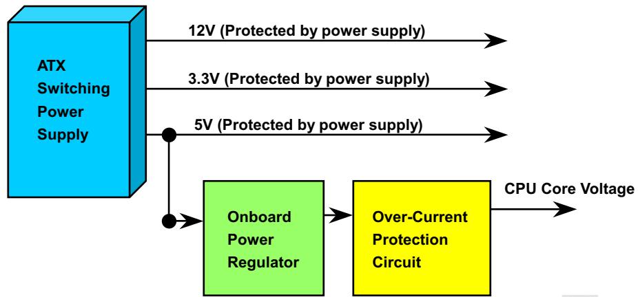
Over-current Protection
The Over Current Protection was very popular implemented on ATX 3.3V/5V/12V switching power supply. However, the new generation CPU uses different voltage that has regulator to transfer 5V to CPU voltage (for example, 2.0V), and makes 5V over current protection useless. This motherboard with switching regulator onboard supports CPU over-current protection, in conjunction with 3.3V/5V/12V power supply provide the full line over-current protection.

Note: Although we have implemented protection circuit try to prevent any human operating mistake, there is still certain risk that CPU, memory, HDD, add-on cards installed on this motherboard may be damaged because of component failure, human operating error or unknown nature reason. AOpen cannot guaranty the protection circuit will always work perfectly.
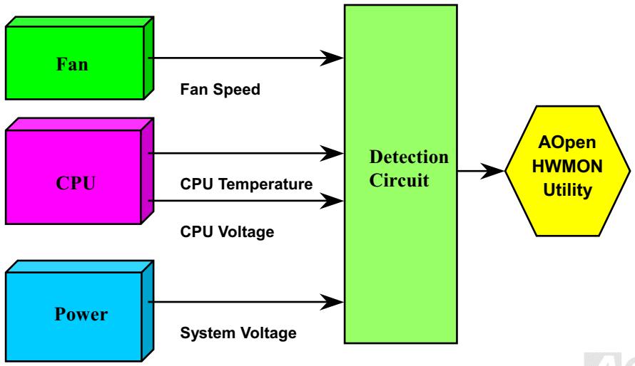
Hardware Monitoring
This motherboard implements a hardware monitoring system. As you turn on your system, this smart design will continue to monitor your system's working voltage, fan status and CPU temperature. If any of these system's status go wrong, there will be an alarm through the AOpen Hardware Monitoring Utility to warn the user.
Resettable Fuse
Traditional motherboard has fuse for Keyboard and USB port to prevent over-current or shortage. These fuses are soldered onboard that when it is broken (did the job to protect motherboard), user still cannot replace it and the motherboard is still malfunction.
With expensive Resettable Fuse, the motherboard can back to normal function after fuse did the protection job.
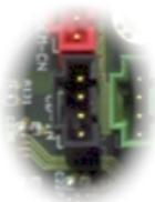
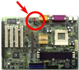
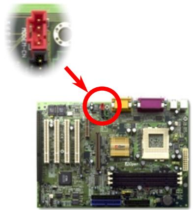
JP30 Die-Hard BIOS (100% Virus Protection)
Recently, many viruses have been found that may destroy bios code and data area. This motherboard implements a very effective hardware protection method that does not involve any software or BIOS coding, hence is 100% virus free.
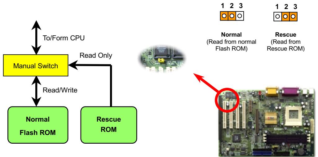
External Controller for DIE-HARD BIOS
External Controller provides you a better and convenience way to switch the BIOS status between "Rescue" and "Normal" without opening the case of your computer. You have to plug the jumper cable to the connector pin on the motherboard. Be careful of the orientation when you connect, the red wire should correspond to Pin1.
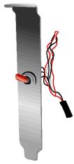
Normal
(Read from normal Flash ROM)
Rescue
(Read from Rescue ROM)

Lock
(Lock your computer to protect your data)

Note: If you suspect your BIOS is infected by virus:
- Turn off the system, set the External Controller to "Rescue" to read from rescue ROM.
- Boot the system and set the switch back to "Normal".
- Follow the BIOS upgrade procedure to rehabilitate BIOS.
- Reboot the system, and you should be able to back to normal.
Tip: If you place the switch to the middle, you will not be able to boot your system, thus you can protect your data from molesting.
Year 2000 (Y2K)
Y2K is basically a problem of the identification of year code. To save storage space, traditional software uses only two digits for year identification. For example, 98 for 1998 and 99 for 1999, but 00 will be confused with 1900 and 2000.
There is an RTC circuit (Real Time Clock) in conjunction with 128 bytes of CMOS RAM data in the chipset of the motherboard. The RTC has only two digits and the CMOS has another 2 digits. Unfortunately, this circuit's behavior is like this 1997 1998 1999 1900 , that means it may have the Y2K problem. Below is a diagram of how applications work with the OS, BIOS and RTC. In order to keep the best compatibility in the PC industry there is a rule that applications must call the OS to get services and OS must call the BIOS, and then only BIOS is allowed to access the hardware (RTC) directly.
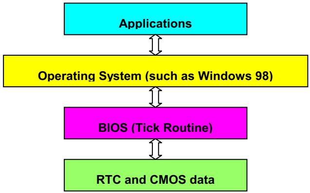
There is a Tick Routine (that goes live around every 50m sec) in the BIOS to keep record of date/time information. In general the BIOS, this Tick Routine does not update the CMOS every time because the CMOS is a very slow device which degrades system performance. The Tick Routine of the AOpen BIOS has 4 digits for year coding, as long as applications and the operating system follow the rule to get date/time information. There will be no Y2K problem (such as NSTL's test program). But unfortunately again, we found some test programs (such as Checkit 98) accesses RTC/CMOS directly. This motherboard has hardware Y2K checking and protection that ensures risk free operation.
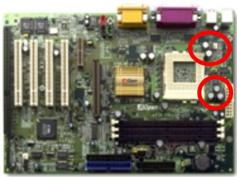
2200uF Low ESR Capacitor
The quality of low ESR capacitor (Low Equivalent Series Resistance) during high frequency operation is very important for stability of CPU power. The location of where to put these capacitors is another know-how that requires experience and detail calculation.
Not only that, this motherboard implements 2200uF capacitors, which is much larger than normal (1000 or 1500uF) and provide better stability for CPU power.
The power circuit of the CPU core voltage must be checked to ensure system stability for high speed CPUs (such as the new Pentium III, or when overclocking). A typical CPU core voltage is 2.0V, so a good design should control voltage between 1.860V and 2.140V. That is, the transient must be below 280mV. Below is a timing diagram captured by a Digital Storage Scope, it shows the voltage transient is only 143mv even when maximum 18A current is applied.
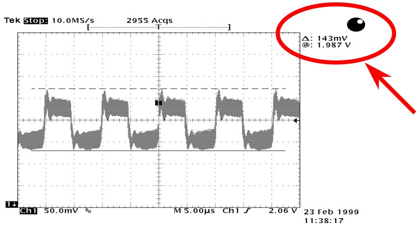
Note: This diagram for example only, it may not be exactly the same as this motherboard.
Layout (Frequency Isolation Wall)
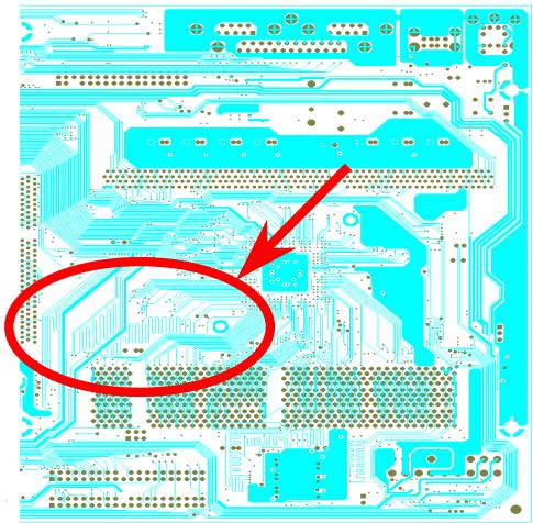
Note: This diagram for example only, it may not be exactly the same as this motherboard.
For high frequency operation, especially overclocking, layout is the most important factor to make sure chipset and CPU working in stable condition. The layout of this motherboard implements AOpen's unique design called " Frequency Isolation Wall". Separating each critical portion of motherboard into regions where each region operates in a same or similar frequency range to avoid crosstalk and frequency interference between each region's operations and condition. The trace length and route must be calculated carefully. For example, the clock trace must be equal length (not necessarily as short as possible) so that clock skew will be controlled within few a pico second (1 / 10^12Sec)
24K Gold Heatsink
Cool down CPU and Chipset is important for system reliability. Gold Heatsink provides better heat consumption especially when you are trying to overclock.
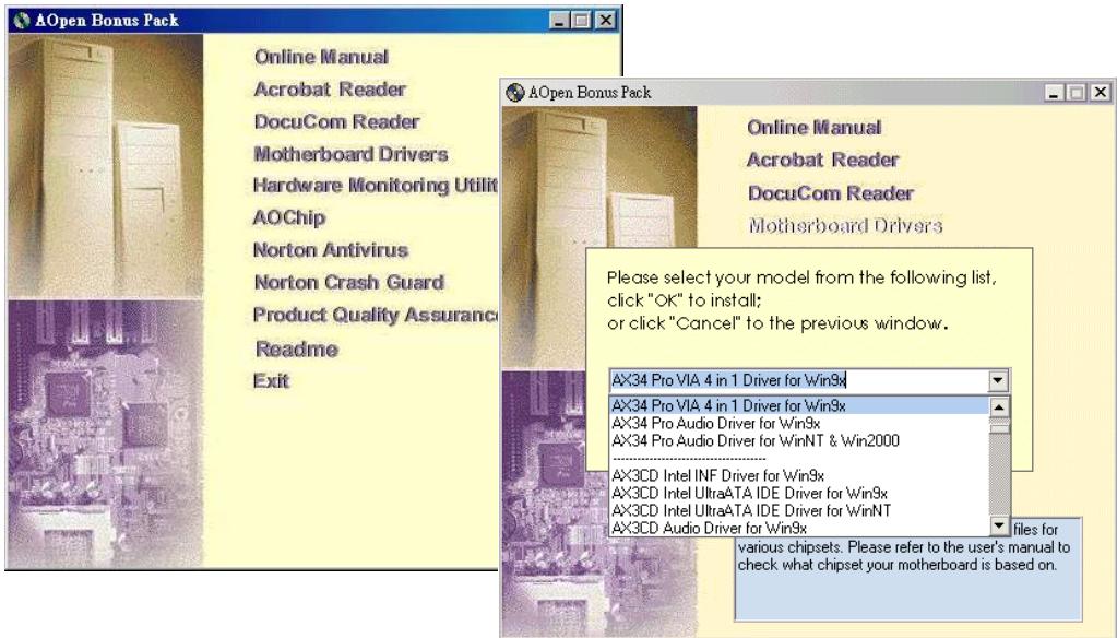
Driver and Utility
There are motherboard drivers and utilities included in AOpen Bonus CD disc. You don't need to install all of them in order to boot your system. But after you finish the hardware installation, you have to install your operation system first (such as Windows 98) before you can install any drivers or utilities. Please refer to your operation system's installation guide.

Note: Please follow recommended procedure to install Windows 95 and Windows 98.
Autorun Menu from Bonus CD Disc
You can use the autorun menu of Bonus CD disc. Choose the utility and driver and select model name.
Installing Windows 95
- First, don't install any add-on card except AGP card.
- Install Windows 95 OSR2 v2.1, 1212 or 1214 version and later with USB support. Otherwise, you need to install USBSUPP.EXE.
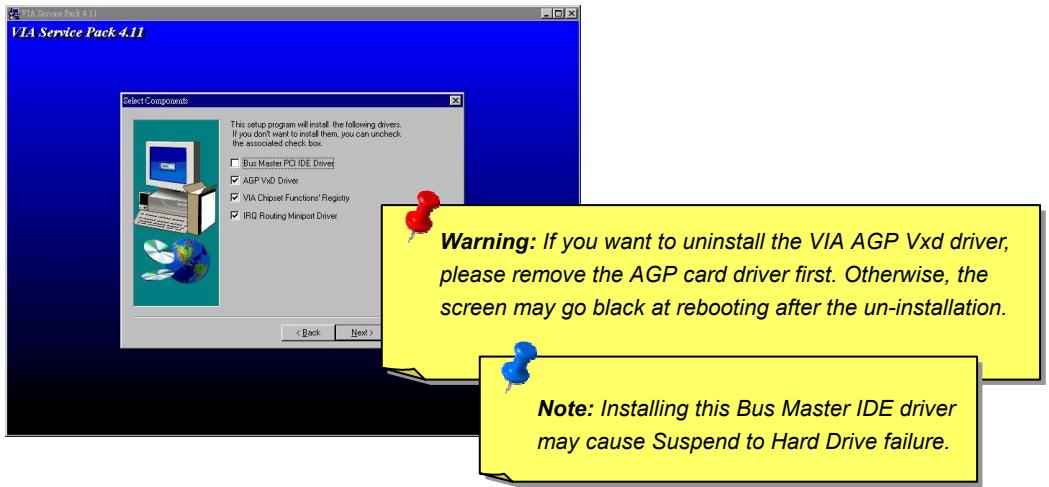
- Install the VIA 4 in 1 driver, which includes VIA AGP Vxd driver, IRQ routing driver, and VIA chipset function registry program.
- Finally, Install other add-on cards and their drivers.
Installing Windows 98
- First, don't install any add-on card except AGP card.
- Enable USB Controller in BIOS Setup > Integrated Peripherals > OnChip USB, to make BIOS fully capable of controlling IRQ assignment.
- Install Window 98 into your system.
- Install the VIA 4 in 1 driver, which includes VIA AGP Vxd driver, IRQ routing driver, and VIA chipset function registry program.
- Finally, Install other add-on cards and their drivers.
Installing Windows 98 SE & Windows2000
If you are using Windows® 98 Second Edition or Windows2000, you do not need to install the 4-in-1 driver as the IRQ Routing Driver and the ACPI Registry are already incorporated into the operating system. Users with Windows® 98 SE may update the IDE Busmaster and AGP drivers by installing them individually.
Please refer to VIA Technologies Inc. for latest version of 4 in 1 driver:
http://www.via.com/
http://www.via.com/drivers/4in1420.exe
Installing VIA 4 in 1 Driver
You can install the VIA 4 in 1 driver (IDE Bus master, VIA AGP, IRQ Routing Driver, VIA Registry) from the Bonus Pack CD disc autorun menu.
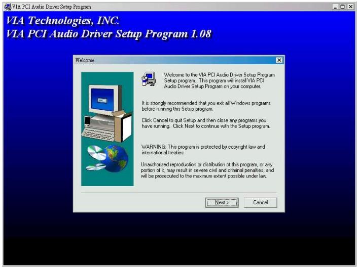
Installing Onboard Sound Driver
This motherboard comes with an AD 1881 AC97 CODEC and the sound controller is in VIA South Bridge chipset. You can find the audio driver from the Bonus Pack CD disc autorun menu.
Installing Hardware Monitoring Utility
You can install Hardware Monitoring Utility to monitor CPU temperature, fans and system voltage. The hardware monitoring function is automatically implemented by the BIOS and utility software, no hardware installation is needed.
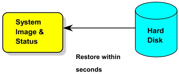
ACPI Suspend to Hard Drive
ACPI Suspend to Hard Drive is basically controlled by Windows operation system. It saves your current work (system status, memory and screen image) into hard disk, and then the system can be totally power off. Next time, when power is on, you can resume your original work directly from hard disk within few seconds without go through the Windows booting process and run your application again. If your memory is 64MB, normally, you need to reserve at least 64MB HDD space to save your memory image.

When go into Suspend:
When power-on next time:
System Requirement
- AOZVHDD.EXE 1.30b or later.
- Delete config.sys and autoexec.bat.
Fresh installation of Windows 98 on a new system
- Execute "Setup.exe /p j" to install Windows 98
- After Windows 98's installation is complete, go to the Control Panel > Power Management.
a. Set Power Schemes > System Standby to "Never".
b. Click on "Hibernate" and select "Enable Hibernate Support" then "Apply".
c. Click on the "Advanced" tab, you'll see "Hibernate" on "Power Buttons". Note that this option will only be seen after step b mentioned above has been completed, otherwise only "Standby" and "Shutdown" will be shown. Select "Hibernate" and "Apply".
- Clean boot into DOS and run AOZVHDD utility.
a. If you assign the whole disk to your Win 98 system (FAT 16 or FAT 32), please run "aozvhdd /c /file". Please remember sufficient free space has to be reserved in the disk, e.g. if you have 64 MB DRAM and 16 MB VGA card installed, the system needs at least 80 MB free space. The utility will locate the space automatically.
b. If you assign an individual partition for Win 98, please run "aozvhdd /c /partition". Of course, the system needs to provide unformatted an empty partition.
- Reboot system.
- You've already implemented ACPI Suspend to-Hard Drive. Click "Start > Shut Down > Standby" then the screen will go off immediately. And 1 minute or so will be taken for the system to save what's in the memory to the hard drive; the larger the memory size the longer this process will take.
Changing from APM to ACPI (Windows 98 only)
1. Run "Regedit.exe"
a. Go through the following path
HKEY_LOCAL_MACHINE
SOFTWARE
MICROSOFT
WINDOWS
CURRENT VERSION
DETECT
b. Select "ADD Binary" and name it as "ACPIOPTION".
c. Right click and select Modify, add "01" after "0000" to make it "0000 01".
d. Save changes.
- Select "Add New Hardware" under Control Panel. Allow Windows 98 to detect new hardware. (It will find "ACPI BIOS" and remove "Plug and Play BIOS")
- Reboot system.
- Clean boot into DOS and run "AOZVHDD.EXE /C /File"
Changing from ACPI to APM
1. Run "Regedit.exe"
a. Go through the following path
HKEY_LOCAL_MACHINE
SOFTWARE
MICROSOFT
WINDOWS
CURRENT VERSION
DETECT
ACPI OPTION
b. Right click and select "Modify, change "01" to "00" to make it "0000 02".

Tip:"02" means Windows 98 is ACPI acknowledged but the ACPI function is disabled.
c. Save changes.
- Select "Add New Hardware" under Control Panel. Allow Windows 98 to detect new hardware. (It will find "Plug and Play BIOS" and remove "ACPI BIOS")
- Reboot system.
- Run "Add New Hardware" again and it will find "Advanced Power Management Resource".
- Click "OK".

Tip: Currently we found only ATI 3D Rage Pro AGP card would support ACPI suspend to disk. Please refer to AOpen web site for latest update.
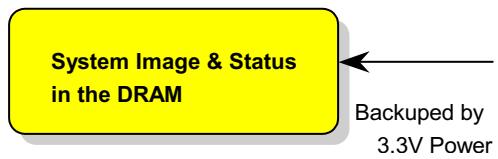
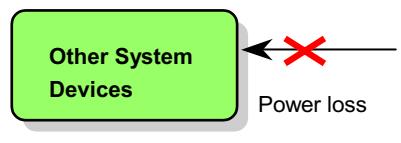
ACPI Suspend to RAM (STR)
This motherboard supports ACPI Suspend to RAM function. With this function, you can resume your original work directly from DRAM without going through the Windows 98 booting process and run your application again. Suspend to DRAM saves your current work in the system memory, it is faster than Suspend to Hard Drive but requires power supplied to DRAM, while Suspend to Hard Drive requires no power.
When go into Suspend:
When power-on next time:

To implement ACPI Suspend to DRAM, please follow the procedures as below:
System Requirement
- An ACPI OS is required. Currently, Windows 98 is the only choice. Please refer to ACPI Suspend to Hard Drive of how to setup Windows 98 ACPI mode.
- The VIA 4 in 1 Driver must have been installed properly.
Procedures
- Changed the following BIOS settings.
BIOS Setup > Power Management > ACPI Function : Enabled
BIOS Setup > Power Management > ACPI Suspend Type :S3.
- Go to Control Panel > Power Management. Set "Power Buttons" to "Standby".
- Press power button or standby button to wake up the system.
AWARD BIOS
System parameters can be modified by going into BIOS Setup menu, this menu allows you to configure the system parameters and save the configuration into the 128 byte CMOS area, (normally in the RTC chip or in the main chipset). To enter to BIOS setup menu, press when POST (Power-On Self Test) screen is shown on your monitor.

Note: Because the BIOS code is the most often changed part of the motherboard design, the BIOS information contained in this manual may be different with actual BIOS that come with your motherboard.
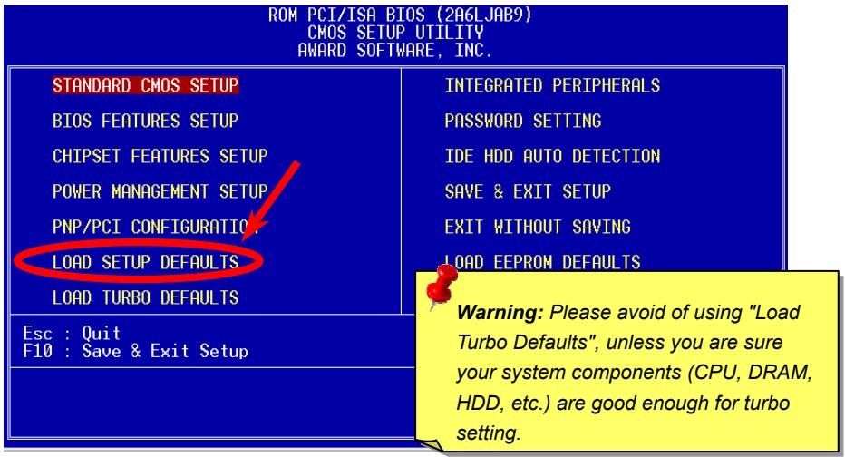
Enter BIOS Setup

After you finish the setting of jumpers and connect correct cables. Power on and enter the BIOS Setup, press during POST (Power-On Self Test). Choose "Load Setup Defaults" for recommended optimal performance.
Change Language

You can change language by press <F9> . Depends on available BIOS space, the possible languages are English, German, Japanese and Chinese.
| ROM PCI/ISA BIOS (2A6LJAB9) CMOS SETUP UTILITY AMARD SOFTWARE, INC. | |
| STANDARD CMOS SETUP | INTEGRATED PERIPHERALS |
| BIOS FEATURES SETUP | password SETTING |
| CHIPSET FEATURES SETUP | IDE HDD AUTO DETECTION |
| POWER MANAGEMENT SETUP | SAVE & EXIT SETUP |
| PNP/PCI CONFIGURATION | EXIT WITHOUT SAVING |
| LOAD SETUP DEFAULTS | LOAD EEPROM DEFAULTS |
| LOAD TURBO DEFAULTS | SAVE EEPROM DEFAULTS |
| Esc: Quit | ↑ ↓ : Select Item |
| F10: Save & Exit Setup | F9 : Change Language |
Standard CMOS Setup

The "Standard CMOS Setup" sets the basic system parameters such as the date, time, and the hard disk type. Use the arrow keys to highlight an item and

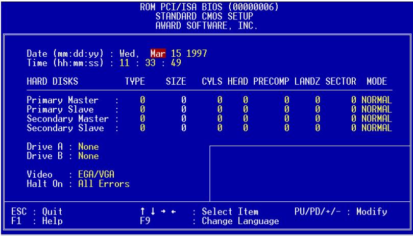


Standard CMOS Setup > Date (mm:dd:yy)
To set the date, highlight the Date parameter. Press <PgUp> or <PgDn> to set the current date. The date format is month, date, and year.
Standard CMOS Setup > Time (hh:mm:ss)
To set the time, highlight the Time parameter. Press <PgUp> or <PgDn> to set the current time in hour, minute, and second format. The time is based on the 24 hour military clock.
Standard CMOS Setup > Primary Master > Type
Standard CMOS Setup > Primary Slave > Type
Standard CMOS Setup > Secondary Master > Type
Standard CMOS Setup > Secondary Slave > Type
Type
Auto
User
None
This item lets you select the IDE hard disk parameters that your system supports.
These parameters are Size, Number of Cylinder, Number of Head, Start Cylinder for Pre-compensation, Cylinder number of Head Landing Zone and Number of Sector per Track. The default setting is Auto, which enables BIOS to automatically detect the parameters of installed HDD (Hard Disk Drive) at POST (Power-On Self Test). If you prefer to enter HDD parameters manually, select User. Select None if no HDD is connected to the system.
The IDE CDROM is always automatically detected.

Tip: For an IDE hard disk, we recommend that you use the "IDE HDD Auto Detection" to enter the drive specifications automatically. See the section "IDE HDD Auto Detection".
Standard CMOS Setup > Primary Master > Mode
Standard CMOS Setup > Primary Slave > Mode
Standard CMOS Setup > Secondary Master > Mode
Standard CMOS Setup > Secondary Slave > Mode
Mode
Auto
Normal
LBA
Large
The enhanced IDE feature allows the system to use a hard disk with a capacity of more than 528MB. This is made possible through the Logical Block Address (LBA) mode translation. The LBA is now considered a standard feature of current IDE hard disk on the market because of its capability to support capacity larger than 528MB. Note that if a HDD is formatted with LBA On, it will not be able to boot with LBA Off.
Standard CMOS Setup > Drive A
Standard CMOS Setup > Drive B
Drive A
None
360KB 5.25"
1.2MB 5.25"
720KB 3.5"
1.44MB 3.5"
2.88MB 3.5"
These items select the floppy drive type. The available settings and types supported by the motherboard are listed to the left.
Standard CMOS Setup > Video
Video
EGA/VGA
CGA40
CGA80
Mono
This item specifies the type of video card in use. The default setting is EGA/VGA. Since current PCs use VGA only, this function is almost useless and may be disregarded in the future.
Standard CMOS Setup > Halt On
Halt On
No Errors
All Errors
All, But
Keyboard
All, But Diskette
All, But Disk/Key
This parameter enables you to control the system stops in case of Power-On Self Test (POST) error.
BIOS Features Setup
This screen appears when you select the option "BIOS Features Setup" from the main menu.
| ROM PCI/ISA BIOS (2A6LJAB9) BIOS FEATURES SETUP AWARD SOFTWARE, INC. | |
| Virus Warning : Enabled | Video BIOS Shadow : Disabled C8000-CBFFF Shadow : Disabled CC000-CFFFF Shadow : Disabled D0000-D3FFF Shadow : Disabled D4000-D7FFF Shadow : Disabled DB000-DBFFF Shadow : Disabled DC000-DFFFF Shadow : Disabled |
| External Cache : Disabled | |
| CPU L2 Cache ECC Checking : Enabled | |
| Processor Number Feature : Enabled | |
| Quick Power On Self Test : Disabled | |
| Boot From LAN First : Disabled | |
| Boot Sequence : A.C,SCSI | |
| Swap Floppy Drive : Disabled | |
| Boot Up Floppy Seek : Disabled | |
| Boot Up NumLock Status : Off | |
| Memory Parity/ECC Check : Disabled | |
| Typematic Rate Setting : Disabled | |
| Typematic Rate (Chars/Sec) : 6 | |
| Typematic Delay (Msec) : 250 | |
| Security Option : Setup | ESC : Quit ↑↓←: Select Item F1 : Help PU/PD+/−: Modify |
| PCI/VGA Palette Snoop : Disabled | F5 : Old Values F9 : Language |
| OS Select For DRAM > 64MB : Non-OS2 | F6 : Load Setup Defaults |
| Show Logo On Screen : Enabled | F7 : Load Turbo Defaults |
BIOS Features Setup > Virus Warning
Virus Warning
Enabled
Disabled
Set this parameter to Enabled to activate the warning message.
This feature protects the boot sector and partition table of your hard disk from virus intrusion. Any attempt during boot up to write to the boot sector of the hard disk drive stops the system and the following warning message appears on the screen. Run an anti-virus program to locate the problem.
!WARNING !
Disk Boot Sector is to be modified Type "Y" to accept write, or "N" to abort write Award Software, Inc.
BIOS Features Setup > External Cache
External Cache
Enabled
Disabled
Enabling this parameter activates the secondary cache.
Disabling the parameter slows down the system. Therefore, we recommend that you leave it enabled unless you are troubleshooting a problem.
BIOS Features Setup > CPU L2 Cache ECC Checking
CPU L2 Cache ECC
Checking
Enabled
Disabled
This item lets you enable or disable L2 Cache ECC checking.
BIOS Features Setup > Processor Number Feature
Processor Number
Feature
Enabled
Disabled
This item is used to enable or disable Pentium III CPU Number Feature.
BIOS Features Setup > Quick Power On Self Test
Quick Power on Self
Test
Enable
Disabled
This parameter speeds up POST by skipping some items that are normally checked.
BIOS Features Setup > Boot From LAN First
Boot From LAN
First
Enable
Disabled
This item is used to boot the system from a network server.
BIOS Features Setup > Boot Sequence
Boot Sequence
A,C,SCSI
C,A,SCSI
C,CDROM,A
CDROM,C,A
CDROM,A,C
D,A,SCSI
E,A,SCSI
F,A,SCSI
SCSI,A,C
SCSI,C,A
C only
LS/ZIP,C
This parameter allows you to specify the system boot up search sequence. The hard disk ID are listed below:
C: Primary master
D: Primary slave
E: Secondary master
F: Secondary slave
LS: LS120
Zip: IOMEGA ZIP Drive
BIOS Features Setup > Swap Floppy Drive
Swap Floppy Drive
Enabled
Disabled
This item allows you to swap floppy drives. For example, if you have two floppy drives (A and B), you can assign the first drive as drive B and the second drive as drive A or vice-versa.
BIOS Features Setup > Boot Up Floppy Seek
Boot Up Floppy
Seek
Enable
Disabled
Setting this item to force the system to seek the status in detail and detects any errors in both floppy drives during POST.
BIOS Features Setup > Boot Up NumLock Status
Boot Up NumLock
Status
On
Off
Setting this parameter to On enables the numeric function of the numeric keypad. Set this parameter to Off to disregard the function. Disabling the numeric function allows you to use the numeric keypad for cursor control.
BIOS Features Setup > Memory Parity/ECC Check
Memory Parity/ECC
Check
Disable
Enable
Set this option enable if the memory installed on the motherboard support Parity/ECC check. The default setting is Disable.
BIOS Features Setup > Typematic Rate Setting
Typematic Rate
Setting
Disable
Enable
Enable this item to force keyboard to repeat rapidly.
BIOS Features Setup > Typematic Rate (Chars/Sec)
Typematic Rate
6
8
10
12
15
20
24
30
This item allows you to control the speed of repeated keystrokes. The default is 30 characters/sec.
BIOS Features Setup > Typematic Delay (Msec)
Typematic Delay
250
500
750
1000
This parameter allows you to control the delay time between the first and the second keystroke (where the repeated keystrokes begin). The typematic delay settings are 250, 500, 750, and 1000 msec.
BIOS Features Setup > Security Option
Security Option
Setup
System
The System option limits access to both the System boot and BIOS setup. A prompt asking you to enter your password appears on the screen every time you boot the system. The Setup option limits access only to BIOS setup. To disable the security option, select Password Setting from the main menu, don't type anything and just press
BIOS Features Setup > PCI/VGA Palette Snoop
PCI/VGA Palette
Snoop
Enabled
Disabled
Enabling this item informs the PCI VGA card to keep silent (and to prevent conflict) when palette register is updated (i.e., accepts data without responding any communication signals). This is useful only when two display cards use the same palette address and plugged in the PCI bus at the same time (such as MPEG or Video capture). In such case, PCI VGA is silent while MPEG/Video capture is set to function normally.
BIOS Features Setup > OS Select for DRAM > 64MB
OS Select for DRAM
64MB
OS/2
Non-OS/2
Set to OS/2 if your system is utilizing an OS/2 operating system and has a memory size of more than 64 MB.
BIOS Features Setup > Show Logo On Screen
Show Logo On
Screen
Enabled
Disabled
This item lets you show or hide AOpen logo on the POST screen.
BIOS Features Setup > Video BIOS Shadow
Video BIOS Shadow
Enabled
Disabled
VGA BIOS Shadowing means to copy video display card BIOS into the DRAM area. This enhances system performance because DRAM access time is faster than ROM.
BIOS Features Setup > C800-CBFF Shadow
BIOS Features Setup > CC00-CFFF Shadow
BIOS Features Setup > D000-D3FF Shadow
BIOS Features Setup > D400-D7FF Shadow
BIOS Features Setup > D800-DBFF Shadow
BIOS Features Setup > DC00-DFFF Shadow
C8000-CBFFF
Shadow
Enabled
Disabled
These six items are for shadowing ROM code on other expansion cards. Before you set these parameters, you need to know the specific addresses of that ROM code. If you do not know this information, enable all the ROM shadow settings.

Note: The F000 and E000 segments are always shadowed because BIOS code occupies these areas.
Chipset Features Setup
The "Chipset Features Setup" includes settings for the chipset dependent features. These features are related to system performance.
ROM PCI/ISA BIOS (2A6LJAB9)
CHIPSET FEATURES SETUP
AWARD SOFTWARE, INC.
Bank 0/1 DRAM Timing
Bank 2/3 DRAM Timing
Bank 4/5 DRAM Timing
SDRAM CAS Latency
DRAM Clock
Memory Hole At 15M-16M
Fast R-W Turn Around
System BIOS Cacheable
Video RAM Cacheable
AGP Mode
AGP Aperture Size
CPU Micro Codes
SDRAM 10ns
SDRAM 10ns
SDRAM 10ons
3
CPU CLK
Disabled
Disabled
Disabled
Disabled
1x
128M
Disabled
Jumperless Setup
Clock Spread Spectrum
CPU Voltage Detected
CPU Voltage Setting
CPU Speed Detected
CPU Clock Frequency
CPU Clock Ratio
Setup CPU Speed
********
off
2.05 V
0 MHz
124.0 MHz
2.0
248.0 MHz

Warning: Make sure you fully understand the items contained in this menu before you try to change anything. You may change the parameter settings to improve system performance. However, it may cause your system to be unstable if the setting is not correct for your system configuration.
Chipset Features Setup > Bank 0/1 DRAM Timing
Chipset Features Setup > Bank 2/3 DRAM Timing
Chipset Features Setup > Bank 4/5 DRAM Timing
Bank 0/1 DRAM
Timing
SDRAM 10ns
SDRAM 8ns
Normal
Medium
Fast
Turbo
Change this item to control the DRAM timing.
The default value is "SDRAM 10ns". Do not change the default value without understanding engineering knowledge.
Chipset Features Setup > SDRAM CAS Latency
SDRAM CAS Latency
2
3
This SDRAM timing is calculated by clocks. Adjust its value affects SDRAM performance, the default setting is 2 clocks. If your system has unstable problem, change 2T to 3T.
Chipset Features Setup > DRAM Clock
DRAMClock
CPU CLK,
CPU CLK -33M,
CPU CLK +33M
The DRAM Clock can be PCI clock x2, x3 or x4 depends on JP29/JP23 FSB/PCI clock ratio. To be easily understood by users who do not overclock, it is displayed here as CPU CLK -33M, CPU CLK and CPU CLK +33M. Actually, it is CPU -PCI CLK, CPU CLK and CPU +PCI CLK.
PCI Clock = CPU FSB Clock / Clock Ratio
| JP29/JP23Clock Ratio | CPU FSB Clock | PCI | BIOS Setting | DRAM Clock |
| 2X | 66 | 33 | CPU, CPU+PCI | 66, 100 |
| 3X | 100 | 33 | CPU-PCI, CPU, CPU+PCI | 66, 100, 133 |
| 3X, overclocking | 112 | 37.3 | CPU-PCI, CPU, CPU+PCI | 74.6, 112, 149.3 |
| 4X | 133 | 33 | CPU-PCI, CPU | 100, 133 |
| 4X, overclocking | 155 | 38.75 | CPU-PCI, CPU | 116.25, 155 |
Chipset Features Setup > Memory Hole At 15M-16M
Memory Hole At
15M-16M
Enabled
Disabled
This option lets you reserve system memory area for special ISA cards. The chipset accesses code/data of these areas from the ISA bus directly. Normally, these areas are reserved for memory mapped I/O card.
Chipset Features Setup > Fast R-W Turn Around
Fast R-W Turn
Around
Enabled
Disabled
Setting this item to synchronize CPU and DRAM timing. The default value is Enable.
Chipset Features Setup > System BIOS Cacheable
System BIOS
Cacheable
Enabled
Disabled
Setting it to Enabled allows the system BIOS data at F0000h-FFFFFFh (in main memory, 64K in all) to be cacheable for a better system performance.
However, if any program writes to this memory range, a system error may result.
Chipset Features Setup > Video RAM Cacheable
Video RAM Cacheable
Enabled
Disabled
This item lets you cache Video RAM A000 and B000.
Chipset Features Setup > AGP Mode
AGP Mode
1X, 2X, 4X
This item allows you to adjust your AGP graphic card speed.
Chipset Features Setup > AGP Aperture Size
AGP Aperture Size
4,8,16,32,64,128M
This item lets you determine the effective size of the AGP
Graphic Aperture.
Chipset Features Setup > CPU Micro Codes
CPU Micro Codes
Enabled
Disabled
The micro codes are used to fix bugs of CPU, we strongly recommend to enable this item for system reliability reason. However, this microcode may slightly reduce CPU performance. We provide this option for your convenience if you like to test it.
Chipset Features Setup > Clock Spread Spectrum
Clock Spread Spectrum
On Off
This item is used to set clock spread spectrum for EMI testing. Normally, you don't need to change the default setting.
Chipset Features Setup > CPU Voltage Detected
CPU Voltage Detected
This motherboard can automatically detect the default CPU voltage and reminds you the correct setting here.
Chipset Features Setup > CPU Voltage Setting
CPU Voltage Setting
1.3V to 3.5V by 0.05V or 0.1V stepping
This item is designed for overclockers. The default setting is auto detected from existing CPU. You may try to adjust by 0.05V or 0.1V stepping (depends on voltage range) for overclocking to a higher FSB clock, however, doing so may seriously damage your CPU.

Warning: High CPU core voltage may be able to increase CPU speed for overclocking, but you may damage the CPU or reduce the CPU lifecycle.
Chipset Features Setup > CPU Speed Detected
CPU Speed Detected
The actual CPU speed is automatically detected and shown here. It may be different with Setup CPU Speed because in some CPUs, the CPU Clock Ratio may be locked by CPU manufacturer.
Chipset Features Setup > CPU Clock Frequency
CPU Clock Frequency
66.8, 75, 83.3, 100, 105, 110, 112, 115, 120, 124, 133, 140, and 150 MHz.
This item lets you set external clock (FSB clock). The correct setting may vary because of different CPU products, refer to your CPU specification for more details.
Chipset Features Setup > CPU Clock Ratio
CPU Clock Ratio
1.5, 2.0, 2.5, 3.0, 3.5
4.0, 4.5, 5.0, 5.5, 6.0
6.5, 7.0, 7.5, 8.0
Intel Pentium II is designed to have different Internal (Core) and External (Bus) frequency. This item lets you select the ratio of Core/Bus frequency. The default value is 3.5x.
Chipset Features Setup > Setup CPU Speed
Setup CPU Speed
The CPU Speed is derived from the product of "CPU Clock Frequency" and "CPU Clock Ratio".
Core Frequency = CPU FSB Clock * CPU Ratio
Power Management Setup
The Power Management Setup screen enables you to control the motherboard green features. See the following screen.
| ROM PCI/ISA BIOS (2A6LJAB9) POWER MANAGEMENT SETUP AWARD SOFTWARE, INC. | ||
| ACPI function | Enabled | Primary INTR ON |
| Power Management | User Define | IRQ3 (COM 2) Disabled |
| PM Control by APM | No | IRQ4 (COM 1) Disabled |
| Video Off Method | Blank Screen | IRQ5 (LPT 2) Disabled |
| ACPI Suspend Type | S1(POS) | IRQ6 (Floppy Disk) Disabled |
| Standby Mode | Disabled | IRQ7 (LPT 1) Disabled |
| Suspend Mode | Disabled | IRQ8 (RTC Alarm) Disabled |
| HDD Power Down | Disabled | IRQ9 (IRQ2 Redir) Disabled |
| Soft-Off by PWRBTN | Delay 4 Sec | IRQ10 (Reserved) Disabled |
| Wake On PCI Card | Disabled | IRQ11 (Reserved) Disabled |
| Wake On Modem | Disabled | IRQ12 (PS/2 Mouse) Disabled |
| Wake On LAN | Disabled | IRQ13 (Coprocessor) Disabled |
| Wake On RTC timer | Enabled | IRQ14 (Hard Disk) Disabled |
| Date (of Month) | 0 | IRQ15 (Reserved) Disabled |
| Timer (hh:mm:ss) | 0:0:0 | |
| VGA | OFF | ESC : Quit ↑↓++ : Select Item |
| LPT & COM | NONE | F1 : Help PU/PD/+/- : Modify |
| HDD & FDD | OFF | F5 : Old Values F9 : Language |
| PCI Master | OFF | F6 : Load Setup Defaults |
| AC PWR Auto Recovery | Former Status | F7 : Load Turbo Defaults |
Power Management Setup > ACPI Function
ACPI Function
Enabled
Disabled
If your OS is ACPI enabled you have to set this item to Enabled, or there may be unexpected errors. If your OS is APM mode, you can remain the Disabled setting.
Power Management Setup > Power Management
Power Management
Max Saving
Min Saving
User Define
Disabled
This function allows you to set the default parameters of power-saving modes. Set to Disable to turn off power management function. Set to User Define to choose your own parameters.
| Mode | Doze | Standby | Suspend | HDD Power Down |
| Min Saving | 1 hour | 1 hour | 1 hour | 15 min |
| Max Saving | 1 min | 1 min | 1 min | 1 min |
Power Management Setup > PM Controlled by APM
PM Controlled by APM
Yes
No
If "Max Saving" is selected, you can turn on this item, transfer power management control to APM (Advanced Power Management) and enhance power saving function. For example, stop CPU internal clock.
Power Management Setup > Video Off Method
Video Off Method
V/H SYNC + Blank
DPMS Support
Blank Screen
This determines the way that monitor is off. Blank Screen writes blanks to video buffer. V/H SYNC+Blank allows BIOS to control VSYNC and HSYNC signals. This function applies only for DPMS (Display Power Management Standard) monitor. The DPMS mode uses DPMS function provided by VGA card.
Power Management Setup > ACPI Suspend Type
ACPI Suspend Type
S1 (POS)
S3 (STR)
This function allows you to select suspend types. S1 is Power On Suspend and S3 is Suspend to RAM.
Power Management Setup > Standby Mode
Standby Mode
Disabled, 10 Sec, 20 Sec, 30 Sec, 40 Sec, 1 Min, 2 Min, 4 Min, 6 Min, 8 Min, 10 Min, 20 Min, 30 Min, 40 Min, 1 Hour.
This item lets you set the period of time after which the system enters into Standby mode. The system activity (or event) is detected by monitoring the IRQ signals or other events (such as I/O).
Power Management Setup > Suspend Mode
Suspend Mode
Disabled, 10 Sec,
20 Sec, 30 Sec,
40 Sec, 1 Min, 2 Min,
4 Min, 6 Min, 8 Min,
10 Min, 20 Min, 30 Min,
40 Min, 1 Hour,
This item lets you set the period of time after which the system enters into Suspend mode.
Power Management Setup > HDD Power Down
HDD Power Down
Disabled, 1 Min, .... 15 Min
This option lets you specify the IDE HDD idle time before the device enters the power down state. This item is independent from the power states previously described in this section (Doze, Standby and Suspend).
Power Management Setup > Soft-Off by PWRBTN
Soft-Off by PWRBTN
Delay 4 sec.
Instant-Off
This is a specification of ACPI and supported by hardware. When Delay 4 sec. is selected, the soft power switch on the front panel can be used to control power On, Suspend and Off. If the switch is pressed less than 4 sec during power On, the system will go into Suspend mode. If the switch is pressed longer than 4 sec, the system will be turned Off. The default setting is Instant-Off, soft power switch is only used to control On and Off, there is no need to press 4 sec, and there is no Suspend.
Power Management Setup > Wake On PCI Card
Wake On PCI Card
Enable
Disable
This is a function of PCI specification 2.2. PCI bus supports standby current to PCI card and PCI card can wakeup system if it detects certain activity.
Power Management Setup > Wake On Modem
Wake On Resume
Enabled
Disabled
This option lets you specify enable or disable Modem Wake Up function.
Power Management Setup > Wake On LAN
Wake On LAN
Enabled
Disabled
This option lets you specify enable or disable LAN Wake Up function.
Power Management Setup > Wake On RTC Timer
Wake On RTC Timer
Enabled
Disabled
The Wake Up Timer is more like an alarm, which wakes up and powers on your system at a pre-defined time for a specific application. It can be set to wake up everyday or on specific date within a month. The date/time is accurate to within a second. This option lets you enable or disable the RTC Wake Up function.
Power Management Setup > Date (of Month)
Date (of Month)
0-31
To specify the date to wake up your system. You must enable the "Wake On RTC Timer" first to set this item.
Power Management Setup > Timer (hh: mm: ss)
Timer (hh: mm: ss)
00:00:00 -
23:59:59
To specify the time to wake up your system. You must enable the "Wake On RTC Timer" first to set this item.
Power Management Setup > VGA
Power Management Setup > LPT & COM
Power Management Setup > HDD & FDD
Power Management Setup > PCI Master
VGA
ON
OFF
To enable or disable the detection of VGA, LPT, COM, HDD, and PCI activities for power down state transition.
Power Management Setup > AC PWR Auto Recovery
AC PWR Auto
Recovery
Former Status
On
Off
A traditional ATX system should remain at power off stage when AC power resumes from power failure. This design is inconvenient for a network server or workstation, without an UPS, that needs to keep power-on. This item is used to solve this problem. Selecting On enabling system to automatically power-on after AC power resumes; in the other hand, the system will remain power-off if you select Off. If Former Status option is selected, the system will power-on or power-off based on the original state.
Power Management Setup > Primary INTR
Primary INTR
ON
OFF
This item is used to enable or disable the detection of IRQ3-15 or NMI interrupt events for power down state transition. Normally, this is applied to network card.
Power Management Setup > IRQ3 (COM 2)
Power Management Setup > IRQ4 (COM 1)
Power Management Setup > IRQ5 (LPT 2)
Power Management Setup > IRQ6 (Floppy Disk)
Power Management Setup > IRQ7 (LPT 1)
Power Management Setup > IRQ8 (RTC Alarm)
Power Management Setup > IRQ9 (IRQ 2 Redir)
Power Management Setup > IRQ10 (Reserved)
Power Management Setup > IRQ11 (Reserved)
Power Management Setup > IRQ12 (PS/2 Mouse)
Power Management Setup > IRQ13 (Coprocessor)
Power Management Setup > IRQ14 (Hard Disk)
Power Management Setup > IRQ15 (Reserved)
IRQ 3 (COM 2)
Primary
Secondary
Disabled
These items are used to enable or disable the detection of IRQ3-15 interrupt events for power down state transition.
PNP/PCI Configuration Setup
The PNP/PCI Configuration Setup allows you to configure the ISA and PCI devices installed in your system. The following screen appears if you select the option "PNP/PCI Configuration" from the main menu.
| ROM PCI/ISA BIOS (2A6LJAB9) PNP/PCI CONFIGURATION AWARD SOFTWARE, INC. | ||
| PNP OS Installed : No Resources Controlled By : Manual | CPU to PCI Write Buffer: Disabled PCI Dynamic Bursting : Disabled PCI Master 0 WS Write : Enabled PCI Delay Transaction : Disabled PCI#2 Access #1 Retry : Disabled AGP Master 1 WS Write : Disabled AGP Master 1 WS Read : Disabled Assign IRQ For USB : Disabled Assign IRQ For VGA : Disabled MODEM Use IRQ : NA Slot 1 Use IRQ No. : Auto Slot 2 Use IRQ No. : Auto Slot 3 Use IRQ No. : Auto Slot 4 Use IRQ No. : Auto | |
| IRQ-3 assigned to : PCI/ISA PnP | ||
| IRQ-4 assigned to : PCI/ISA PnP | ||
| IRQ-5 assigned to : PCI/ISA PnP | ||
| IRQ-7 assigned to : PCI/ISA PnP | ||
| IRQ-9 assigned to : PCI/ISA PnP | ||
| IRQ-10 assigned to : PCI/ISA PnP | ||
| IRQ-11 assigned to : PCI/ISA PnP | ||
| IRQ-12 assigned to : PCI/ISA PnP | ||
| IRQ-14 assigned to : PCI/ISA PnP | ||
| IRQ-15 assigned to : PCI/ISA PnP | ||
| DMA-0 assigned to : PCI/ISA PnP | ||
| DMA-1 assigned to : PCI/ISA PnP | ESC : Quit ↑↓← : Select Item F1 : Help PU/PD/+/− : Modify F5 : Old Values F9 : Language F6 : Load Setup Defaults F7 : Load Turbo Defaults | |
| DMA-3 assigned to : PCI/ISA PnP | ||
| DMA-5 assigned to : PCI/ISA PnP | ||
| DMA-6 assigned to : PCI/ISA PnP | ||
| DMA-7 assigned to : PCI/ISA PnP | ||
PNP/PCI Configuration > PNP OS Installed
PNP OS Installed
Yes
No
Normally, the PnP resources are allocated by BIOS during POST (Power-On Self Test). If you are using a PnP operating system (such as Windows 95), set this item to Yes to inform BIOS to configure only the resources needed for booting (VGA/IDE or SCSI). The rest of system resources will be allocated by PnP operating system.
PNP/PCI Configuration > Resources Controlled By
Resources Controlled
By
Auto
Manual
Setting this option to Manual allows you to individually assign the IRQs and DMAs to the ISA and PCI devices. Set this to Auto to enable the auto-configuration function.
PNP/PCI Configuration > IRQ3 assigned to
PNP/PCI Configuration > IRQ4 assigned to
PNP/PCI Configuration > IRQ5 assigned to
PNP/PCI Configuration > IRQ7 assigned to
PNP/PCI Configuration > IRQ9 assigned to
PNP/PCI Configuration > IRQ10 assigned to
PNP/PCI Configuration > IRQ11 assigned to
PNP/PCI Configuration > IRQ12 assigned to
PNP/PCI Configuration > IRQ14 assigned to
PNP/PCI Configuration > IRQ15 assigned to
IRQ 3 assigned to
Legacy ISA
PCI/ISA PnP
If your ISA card is not PnP compatible and requires a special IRQ to support its function, set the selected IRQ to Legacy ISA. This setting informs the PnP BIOS to reserve the selected IRQ for the installed legacy ISA card. The default is PCI/ISA PnP. Take note that PCI cards are always PnP compatible (except old PCI IDE card).
PNP/PCI Configuration > DMA 0 assigned to
PNP/PCI Configuration > DMA 1 assigned to
PNP/PCI Configuration > DMA 3 assigned to
PNP/PCI Configuration > DMA 5 assigned to
PNP/PCI Configuration > DMA 6 assigned to
PNP/PCI Configuration > DMA 7 assigned to
DMA 0 assigned to
Legacy ISA PCI/ISA PnP
If your ISA card is not PnP compatible and requires a special DMA channel to support its function, set the selected DMA channel to Legacy ISA. This setting informs the PnP BIOS to reserve the selected DMA channel for the installed legacy ISA card. The default is PCI/ISA PnP. Take note that PCI card does not require DMA channel.
PNP/PCI Configuration > CPU to PCI Write Buffer
CPU to PCI Write Buffer
Enable Disable
This item is used to enable or disable CPU to PCI write buffer.
PNP/PCI Configuration > PCI Dynamic Bursting
PCI Dynamic Bursting
Enable
Disable
This item is used to enable or disable PCI dynamic bursting.
PNP/PCI Configuration > PCI Master 0 WS Write
PCI Master 0 WS
Write
Enable
Disable
This item is used to control the PCI master write cycle. If enabled, there is no wait state. If disabled, there will be one wait state for PCI master write.
PNP/PCI Configuration > PCI Delay Transaction
PCI Delay Transaction
Enable
Disable
This item lets you control the Delayed Transaction function of the VIA 586A chipset (Intel PCI to ISA bridge). This function is used to meet latency of PCI cycles to or from ISA bus. Try to enable or disable it, if you have ISA card compatibility problem.
PNP/PCI Configuration > PCI#2 Access #1 Retry
PCI#2 Access #1
Retry
Enable
Disable
This item is used to enable or disable AGP master retry disconnect. If enabled, AGP master will be disconnected if max retries are attempted without success. PCI#2 means AGP.
PNP/PCI Configuration > AGP Master 1 WS Write
AGP Master 1 WS
Write
Enable
Disable
This item is used to enable or disable AGP master 1 wait state write.
PNP/PCI Configuration > AGP Master 1 WS Read
AGP Master 1 WS
Read
Enable
Disable
This item is used to enable or disable AGP master 1 wait state read.
PNP/PCI Configuration > Assign IRQ for USB
Assign IRQ for USB
Enabled
Disabled
This item lets you set an IRQ for USB.
PNP/PCI Configuration > Assign IRQ for VGA
Assign IRQ for VGA
Enabled
Disabled
This item lets you set an IRQ for VGA.
PNP/PCI Configuration > Modem Use IRQ
Modem Use IRQ
3, 4, 5, 7, 9, 10, 11, N/A
This item lets you set an IRQ for the modem.
PNP/PCI Configuration > Slot 1 IRQ No.
PNP/PCI Configuration > Slot 2 IRQ No.
PNP/PCI Configuration > Slot 3 IRQ No.
PNP/PCI Configuration > Slot 4 IRQ No.
Slot1 IRQ No.
3,4,5,6,7,9,10,11, 12,14,15,Auto
This item is reserved for engineering purpose to let you assign an IRQ manually to the add-on card on each PCI slot. If you select Auto, system will automatically assign an available value to the device.
It is suggested to use default setting, which is Auto, in order to comply with PnP specification completely.
Load Setup Defaults
The "Load Setup Defaults" option loads optimized settings for optimum system performance.
Optimal settings are relatively safer than the Turbo settings. All the product verification,
compatibility/reliability test report and manufacture quality control are based on "Load
Setup Defaults". We recommend to use this settings for normal operation. "Load Setup Defaults"
is not the slowest setting for this motherboard. If you need to verify an unstable problem, you may
manually set the parameter in the "BIOS Features Setup" and "Chipset Features Setup" to get
slowest and safer setting.
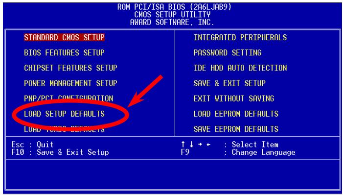
Load Turbo Defaults
The "Load Turbo Defaults" option gives better performance than "Load Setup Defaults". It is provided for the convenience of power user who wants to push the motherboard to get better performance. Turbo setting does not go though all the detail reliability and compatibility test, it is tested only with limited configuration and loading (for example, a system that contains only a VGA card and two DIMMs). Use Turbo setting only when you fully understand the items in Chipset Setup menu. The performance improvement of Turbo setting is normally around 3% to 5% , depending on the chipset and the application.
Integrated Peripherals
The following screen appears if you select the option "Integrated Peripherals" from the main menu. This option allows you to configure the I/O features.
| ROM PCI/ISA BIOS (2A6LJAB9) INTEGRATED PERIPHERALS AWARD SOFTWARE, INC. | ||
| OnChip Primary IDE : Enabled OnChip Secondary IDE : Enabled IDE Prefetch Mode : Enabled IDE HDD Block Mode : Enabled Primary Master PIO : Auto Primary Slave PIO : Auto Secondary Master PIO : Auto Secondary Slave PIO : Auto Primary Master UDMA : Auto Primary Slave UDMA : Auto Secondary Master UDMA : Auto Secondary Slave UDMA : Auto Init Display First : PCI Slot | Onboard FDD Controller: Enabled Onboard Serial Port 1 : Auto Onboard Serial Port 2 : 3F8/IRQ4 UART 2 Mode : HPSIR IR Function Duplex : Full RxD, TxD Active : Hi, Hi Onboard Parallel Port : 3BC/IRQ7 Onboard Parallel Mode : ECP/EPP ECP Mode Use DMA : 1 Parallel Port EPP Type : EPP1.7 OnChip USB : Enabled USB Keyboard Support : Disabled | |
| AMR Function : Enabled | ||
| OnChip Sound : Enabled OnChip Legacy Audio : Enabled Sound I/O Base Address : 220H Sound IRQ Select : IRQ 5 Sound DMA Select : DMA 0 MPU-401 I/O Address : 300-303H | ESC : Quit ↑↓← : Select Item F1 : Help PU/PD/+/:- : Modify F5 : Old Values F9 : Language F6 : Load Setup Defaults F7 : Load Turbo Defaults | |
Integrated Peripherals > OnChip Primary IDE
Integrated Peripherals > OnChip Secondary IDE
OnChip Primary IDE
Enabled
Disabled
This parameter lets you enable or disable the IDE device connected to the primary IDE connector.
Integrated Peripherals > IDE Prefetch Mode
IDE Prefetch Mode
Enabled
Disabled
This item is used to enable and disable IDE prefetch mode.
Integrated Peripherals > IDE HDD Block Mode
IDE HDD Block Mode
Enabled
Disabled
This feature enhances disk performance by allowing multi-sector data transfers and eliminates the interrupt handling time for each sector. Most IDE drives, except with old designs, can support this feature.
Integrated Peripherals > Primary Master PIO
Integrated Peripherals > Primary Slave PIO
Integrated Peripherals > Secondary Master PIO
Integrated Peripherals > Secondary Slave PIO
Primary Master PIO
Auto
Mode 1
Mode 2
Mode 3
Mode 4
Setting this item to Auto activates the HDD speed auto-detect function. The PIO mode specifies the data transfer rate of HDD. For example: mode 0 data transfer rate is 3.3MB/s, mode 1 is 5.2MB/s, mode 2 is 8.3MB/s, mode 3 is 11.1MB/s and mode 4 is 16.6MB/s. If your hard disk performance becomes unstable, you may manually try the slower mode.
Integrated Peripherals > Primary Master UDMA
Integrated Peripherals > Primary Slave UDMA
Integrated Peripherals > Secondary Master UDMA
Integrated Peripherals > Secondary Slave UDMA
Primary Master UDMA
Auto
Disabled
This item allows you to set the ATA/66 mode supported by the hard disk drive connected to your primary IDE connector.
Integrated Peripherals > Init Display First
Init Display First
PCI Slot
AGP
If you installed a PCI VGA card and an AGP card at the same time, this item lets you decide which one is the initial display card.
Integrated Peripherals > OnChip Sound
OnChip Sound
Enable
Disable
This item is used to enable or disable the onboard audio.
Integrated Peripherals > OnChip Legacy Audio
OnChip Legacy Audio
Enable
Disable
This motherboard has a Sound Blaster Pro compatible onchip audio. This item should be set to Enabled under DOS mode.
Integrated Peripherals > Sound I/O Base Address
Sound I/O Base
Address
220H, 240H, 260H,
280H
This item is used to select Sound Blaster compatible I/O base address for the onboard audio.
Integrated Peripherals > Sound IRQ Select
Sound IRQ Select
IRQ5, IRQ7, IRQ9,
IRQ10
This item is used to select Sound Blaster compatible IRQ for the onboard audio.
Integrated Peripherals > Sound DMA Select
Sound DMA Select
DMA0, DMA1,
DMA2, DMA3
This item is used to select Sound Blaster compatible DMA for the onboard audio.
Integrated Peripherals > MPU-401 I/O Address
MPU-401 I/O Address
300-303H
310-313H
320-323H
330-333H
This item is used to select I/O base address for the MIDI port.
Integrated Peripherals > Onboard FDD Controller
Onboard FDD
Controller
Enabled
Disabled
Setting this parameter to Enabled allows you to connect your floppy disk drives to the onboard floppy disk connector instead of a separate controller card. Change the setting to Disabled if you want to use a separate controller card.
Integrated Peripherals > Onboard Serial Port 1
Integrated Peripherals > Onboard Serial Port 2
Onboard Serial Port 1
Auto
3F8/IRQ4
2F8/IRQ3
3E8/IRQ4
2E8/IRQ3
Disabled
This item allows you to assign address and interrupt for the board serial port. Default is Auto.

Note: If you are using network card, make sure that the IRQ do not conflict.
Integrated Peripherals > UART 2 Mode
UART 2 Mode
Standard
HPSIR
ASKIR
This item is configurable only if the "Onboard Serial Port 2" is enabled. This allows you to specify the mode of serial port2. The available mode selections are:
Standard
Sets serial port 2 to operate in normal mode. This is the default setting.
HPSIR
This setting allows infrared serial communication at a maximum baud rate of 115K baud.
ASKIR
This setting allows infrared serial communication at a maximum baud rate of 19.2K baud.
Integrated Peripherals > IR Function Duplex
IR Function Duplex
Full
Half
This item is used to select Full Duplex or Half Duplex of IR function. Normally, Full Duplex is faster, because it transmits data bi-direction at the same time.
Integrated Peripherals > RxD, TxD Active
RxD, TxD Active
Hi, Hi
Hi, Lo,
Lo, Hi
Lo, Lo
This item is used to select RxD (Receive Data) and TxD (Transmit Data) mode for UART 2, when used for IR function. Please refer to the documentation that comes v your IR device.
Integrated Peripherals > Onboard Parallel Port
Onboard Parallel Port
3BC/IRQ7
378/IRQ7
278/IRQ5
Disabled
This item controls the onboard parallel port address and interrupt.

Note: If you are using an I/O card with a parallel port, make sure that the addresses and IRQ do not conflict.
Integrated Peripherals > Onboard Parallel Mode
Onboard Parallel
Mode
Normal
SPP
ECP
EPP
ECP/EPP
This item lets you set the parallel port mode. The mode options are SPP (Standard and Bi-directional Port), EPP (Enhanced Parallel Port) and ECP (Extended Parallel Port).
SPP (Standard and Bidirection Parallel Port)
SPP is the IBM AT and PS/2 compatible mode.
EPP (Enhanced Parallel Port)
EPP enhances the parallel port throughput by directly writing/reading data to/from parallel port without latch.
ECP (Extended Parallel Port)
ECP supports DMA and RLE (Run Length Encoded) compression and decompression.
Integrated Peripherals > ECP Mode Use DMA
ECP Mode Use DMA
3
1
This item lets you set the DMA channel of ECP mode.
Integrated Peripherals > Parallel Port EPP Type
Parallel Port EPP
Type
EPP1.7
EPP1.9
This item lets you select EPP mode protocol.
Integrated Peripherals > OnChip USB
OnChip USB
Enabled
Disabled
This item is used to enable or disable USB controller.
Integrated Peripherals > USB Keyboard Support
USB Keyboard
Support
Enabled
Disabled
This item lets you enable or disable the USB keyboard driver within the onboard BIOS. The keyboard driver simulates legacy keyboard command and let you use USB keyboard during POST or after boot if you don't have USB driver in the operating system.

Note: You cannot use both USB driver and USB legacy keyboard at the same time. Disable "USB Keyboard Support" if you have USB driver in the operating system.
Integrated Peripherals > AMR Function
AMR Function
Enabled
Disabled
The item is used to enable or disable the AC97 modem. If disabled, an AMR modem card can't work properly.
Password Setting
Password prevents unauthorized use of your computer. If you set a password, the system prompts for the correct password before boot or access to Setup.
To set a password:
- At the prompt, type your password. Your password can be up to 8 alphanumeric characters. When you type the characters, they appear as asterisks on the password screen box.
- After typing the password, press.
- At the next prompt, re-type your password and press again to confirm the new password. After the password entry, the screen automatically reverts to the main screen.
To disable the password, press when prompted to enter the password. The screen displays a message confirming that the password has been disabled.
IDE HDD Auto Detection
If your system has an IDE hard drive, you can use this function to detect its parameters and enter them into the "Standard CMOS Setup" automatically.
| ROM PCI/ISA BIOS (2A6LJAB9) CMOS SETUP UTILITY AWARD SOFTWARE, INC. | |
| STANDARD CMOS SETUP | INTEGRATED PERIPHERALS |
| BIOS FEATURES SETUP | password setting |
| CHIPSET FEATURES SETUP | IDE HDD AUTO DETECTION |
| POWER MANAGEMENT SETUP | SAVE & EXIT SETUP |
| PNP/PCI CONFIGURATION | EXIT WITHOUT SAVING |
| LOAD SETUP DEFAULTS | LOAD EEPROM DEFAULTS |
| LOAD TURBO DEFAULTS | SAVE EEPROM DEFAULTS |
| Esc: Quit | ↑ ↓ → ← : Select Item |
| F10: Save & Exit Setup | F9 : Change Language |
This routine only detects one set of parameters for your IDE hard drive. Some IDE drives can use more than one set of parameters. If your hard disk is formatted using different parameters than those detected, you have to enter the parameters manually. If the parameters listed do not match the ones used to format the disk, the information on that disk will not be accessible. If the auto-detected parameters displayed do not match those that used for your drive, ignore them. Type "N" to reject the values and enter the correct ones manually from the Standard CMOS Setup screen.
Save & Exit Setup
This function automatically saves all CMOS values before leaving Setup.
| ROM PCI/ISA BIOS (2A6LJAB9) CMOS SETUP UTILITY AWARD SOFTWARE, INC. | |
| STANDARD CMOS SETUP | INTEGRATED PERIPHERALS |
| BIOS FEATURES SETUP | password SETTING |
| CHIPSET FEATURES SETUP | IDE HDD AUTO DETECTION |
| POWER MANAGEMENT SETUP | SAVE & EXIT SETUP |
| PNP/PCI CONFIGURATION | EXIT WITHOUT SAVING |
| LOAD SETUP DEFAULTS | LOAD EEPROM DEFAULTS |
| LOAD TURBO DEFAULTS | SAVE EEPROM DEFAULTS |
| Esc: Quit | ↑ ↓ → : Select Item |
| F10: Save & Exit Setup | F9 : Change Language |
Load EEPROM Default
Except "Load Setup Default" and "Load Turbo Default", you may also use "Save EEPROM Default" to save your own settings into EEPROM, and reload by using this item.
Save EEPROM Default
You may use this item to save your own settings into EEPROM. Then, if the data in CMOS is lost or you forget the previous settings, you may use "Load EEPROM Default" to reload.
Exit without Saving
Use this function to exit Setup without saving the CMOS value changes. Do not use this option if you want to save the new configuration.
NCR SCSI BIOS and Drivers
Due to Flash ROM space limitation, some BIOS versions do not include NCR 53C810 SCSI BIOS (supports DOS, Windows 3.1 and OS/2) into the system BIOS. Many SCSI cards have its own SCSI BIOS on card, for better system performance, you may use the drivers that come with the NCR SCSI card or with your operating system. For details, refer to the installation manual of your NCR 53C810 SCSI card.
BIOS Upgrade
AOpen Easy Flash is more user friendly than traditional flash method. The BIOS binary file and flash routine are combined together and you simply run a single file to complete the flash process.
- Get new BIOS upgrade program from AOpen's web site. For example, AX34P109.EXE. It is recommended to save it to a bootable DOS floppy diskette for error recovery.
- Reboot the system to DOS mode without loading any memory handler (such as EMM386) or device driver. It needs around 520K free memory space.
- Execute A:> AX34P109
DO NOT turn off the power during FLASH PROCESS.

- Reboot system and press
to enter BIOS setup, Choose "Load Setup Defaults", then "Save & Exit Setup". Done!

Warning: The upgrade of new BIOS will permanently replace your original BIOS content after flashing. The original BIOS setting and Win95/Win98 PnP information will be refreshed and you probably need to re-configure your system.
Overclocking
As a leading manufacturer in motherboard industry, AOpen always listens to what customers want and develop products to fit different user's requirements. Reliability, compatibility, leading technology and friendly features are our basic goals when designing motherboards. Other than above mentioned design criteria, there are power users who are always seeking to push the limitation of the system performance by overclocking which we call them "Overclocker".
This section is dedicated to Overclockers.
This high performance motherboard is designed for maximum 133MHz CPU bus clock. But it comes with clock generator of 150MHz when we design it to accommodate future CPU bus clock. Our lab test results shown that 150MHz is achievable when proper setting and qualified components were presented.

Warning: The design of this product follows CPU and chipset vendor's design guideline. Any attempts to push beyond product specification are not recommended and you are taking your own risk to damage your system or important data. Before doing overclocking, you must make sure your components are able to tolerate such abnormal setting, especially CPU, memory, hard disks, and AGP VGA cards.

Tip: Note that overclocking may also cause thermal problem. Please make sure that the cooling fan and the heatsink were adequate to dissipate excessive heat that's generated by overclocking the CPU.
VGA and HDD
VGA and HDD are key components for overclocking, following list are what have been tested in our lab. Please note that AOpen can not guaranty they can be successful overclocked again.
VGA: http://www.aopen.com.tw/tech/report/overclk.mb/vga-oc.htm
HDD: http://www.aopen.com.tw/tech/report/overclk.mb/hdd-oc.htm
Glossary
AC97
Basically, AC97 specification separates sound/modem circuit to two parts, digital processor and a CODEC for analog I/O, they are linked by AC97 link bus. Since digital processor can be put into motherboard main chipset, the cost of sound/modem onboard solution can be reduced.
ACPI (Advanced Configuration & Power Interface)
ACPI is the power management specification of PC97 (1997). It intends to save more power by taking full control of power management to operating system and bypass BIOS. The chipset or super I/O chip needs to provide standard register interface to operating system (such as Windows 98). This is a bit similar as the PnP register interface. ACPI defines ATX momentary soft power switch to control the power state transition.
AGP (Accelerated Graphic Port)
AGP is a bus interface targeted for high-performance 3D graphic. AGP supports only memory read/write operation and single-master single-slave one-to-one only. AGP uses both rising and falling edge of the 66MHz clock, for 2X AGP, the data transfer rate is 66MHz× 4 byte × 2 = 528MB / s . AGP is now moving to 4X mode, 66MHz× 4 byte × 4 = 1056MB / s . AOpen is the first company to support 4X AGP motherboards by both AX6C (Intel 820) and MX64/AX64 (VIA 694x), started from Oct 1999.
AMR (Audio/Modem Riser)
The CODEC circuit of AC97 sound/modem solution can be put on motherboard or put on a riser card (AMR card) that connects to motherboard through AMR connector.
AOpen Bonus Pack CD
A disc bundled with AOpen motherboard product, there are motherboard drivers, Acrobat Reader for PDF online manual and other useful utilities.
APM
Unlike ACPI, BIOS controls most APM power management functions. AOpen Suspend to Hard Drive is a good example of APM power management.
ATA/66
ATA/66 uses both rising edge and falling edge but doubles UDMA/33 transfer rate. The data transfer rate is 4 times of the PIO mode 4 or DMA mode 2, 16.6MB/s x4 = 66MB/s. To use ATA/66, you need special ATA/66 IDE cable.
ATA/100
ATA/100 is a new IDE specification under developing. ATA/100 uses both rising edge and falling edge as ATA/66 but clock cycle time is reduced to 40ns. The data transfer rate is (1/40ns) x 2 bytes x 2 = 100MB/s. To use ATA/100, you need special 80-wire IDE cable, the same as ATA/66.
BIOS (Basic Input/Output System)
BIOS is a set of assembly routine/program that reside in EPROM or Flash ROM. BIOS controls Input/output devices and other hardware devices of motherboard. In general, to provide hardware independent portability, operation system and drivers is required to access BIOS without directly access hardware devices.
Bus Master IDE (DMA mode)
The traditional PIO (Programmable I/O) IDE requires the CPU to involve in all the activities of the IDE access including waiting for the mechanical events. To reduce the workload of the CPU, the bus master IDE device transfers data from/to memory without interrupting CPU, and releases CPU to operate concurrently while data is transferring between memory and IDE device. You need the bus master IDE driver and the bus master IDE HDD to support bus master IDE mode.
CODEC (Coding and Decoding)
Normally, CODEC means a circuit that can do digital to analog conversion and also the analog to digital conversion. It is part of AC97 sound/modem solution.
DIMM (Dual In Line Memory Module)
DIMM socket has total 168-pin and supports 64-bit data. It can be single or double side, the golden finger signals on each side of PCB are different, that is why it was called Dual In Line. Almost all DIMMs are made by SDRAM, which operate at 3.3V. Note that some old DIMMs are made by FPM/EDO and only operate at 5V. Do not confuse them with SDRAM DIMM..
ECC (Error Checking and Correction)
The ECC mode needs 8 ECC bits for 64-bit data. Each time memory is accessed, ECC bits are updated and checked by a special algorithm. The ECC algorithm has the ability to detect double-bit error and automatically correct single-bit error while parity mode can only detect single-bit error.
EDO (Extended Data Output) Memory
The EDO DRAM technology is actually very similar to FPM (Fast Page Mode). Unlike traditional FPM that tri-states the memory output data to start the pre-charge activity, EDO DRAM holds the memory data valid until the next memory access cycle, that is similar to pipeline effect and reduces one clock state.
EEPROM (Electronic Erasable Programmable ROM)
Also known as E^2PROM . Both EEPROM and Flash ROM can be re-programmed by electronic signals, but the interface technology is different. Size of EEPROM is much smaller than flash ROM, AOpen motherboard uses EEPROM for jumper-less and battery-less design.
EPROM (Erasable Programmable ROM)
Traditional motherboard stores BIOS code in EPROM. EPROM can only be erased by ultra-violet (UV) light. If BIOS has to be upgraded, you need to remove EPROM from motherboard, clear by UV light, re-program, and then insert back.
FCC DoC (Declaration of Conformity)
The DoC is component certification standard of FCC EMI regulations. This standard allows DIY component (such as motherboard) to apply DoC label separately without a shielding of housing.
FC-PGA
FC means Flip Chip, FC-PGA is a new package of Intel for Pentium III CPU. It can plug into SKT370 socket, but require motherboard to add some signals on socket 370. That is, the motherboard needs to be redesigned. Intel is going to ship FC-PGA 370 CPU and phase out slot1 CPU.
Flash ROM
Flash ROM can be re-programmed by electronic signals. It is easier for BIOS to upgrade by a flash utility, but it is also easier to be infected by virus. Because of increase of new functions, BIOS size is increased from 64KB to 256KB (2M bit). AOpen AX5T is the first board to implement 256KB (2Mbit) Flash ROM. Now flash ROM size is moving to 4M bit on AX6C (Intel 820) and MX3W (Intel 810) motherboard.
FSB (Front Side Bus) Clock
FSB Clock means CPU external bus clock.
CPU internal clock = CPU FSB Clock x CPU Clock Ratio
I2C Bus
See SMBus.
P1394
P1394 (IEEE 1394) is a standard of high-speed serial peripheral bus. Unlike low or medium speed USB, P1394 supports 50 to 1000Mbit/s and can be used for video camera, disk and LAN.
Parity Bit
The parity mode uses 1 parity bit for each byte, normally it is even parity mode, that is, each time the memory data is updated, parity bit will be adjusted to have even count "1" for each byte. When next time, if memory is read with odd number of "1", the parity error is occurred and this is called single bit error detection.
PBSRAM (Pipelined Burst SRAM)
For Socket 7 CPU, one burst data read requires four QWord (Quad-word, 4 × 16 = 64 bits). PBSRAM only needs one address decoding time and automatically sends the remaining QWords to CPU according to a predefined sequence. Normally, it is 3-1-1-1, total 6 clocks, which is faster than asynchronous SRAM. PBSRAM is often used on L2 (level 2) cache of Socket 7 CPU. Slot 1 and Socket 370 CPU do not need PBSRAM.
PC100 DIMM
SDRAM DIMM that supports 100MHz CPU FSB bus clock.
PC133 DIMM
SDRAM DIMM that supports 133MHz CPU FSB bus clock.
PDF Format
A file format for electronic document, PDF format is independent from platform, you can read PDF file under Windows, Unix, Linux, Mac ... with different PDF reader. You can also read PDF file by web browser such as IE and Netscape, note that you need to install PDF plug-in first (Included in Acrobat Reader).
PnP (Plug and Play)
The PnP specification suggests a standard register interface for both BIOS and operating system (such as Windows 95). These registers are used by BIOS and operating system to configure system resource and prevent any conflicts. The IRQ/DMA/Memory will be automatically allocated by PnP BIOS or operating system. Currently, almost all the PCI cards and most ISA cards are already PnP compliant.
POST (Power-On Self Test)
The BIOS self test procedure after power-on, sometimes, it is the first or the second screen shown on your monitor during system boot.
RDRAM (Rambus DRAM)
Rambus is a memory technology that uses large burst mode data transfer. Theoretically, the data transfer should be high than SDRAM. RDRAM is cascaded in channel operation. For Intel 820, only one RDRAM channel is supported, 16-bit data per channel, and this channel may have maximum 32 RDRAM devices, no matter how many RIMM sockets.
RIMM
184-pin memory module that supports RDRAM memory technology. A RIMM memory module may contain up to maximum of 16 RDRAM devices.
SDRAM (Synchronous DRAM)
SDRAM is one of the DRAM technologies that allows DRAM to use the same clock as the CPU host bus (EDO and FPM are asynchronous and do not have clock signal). It is similar as PBSRAM to use burst mode transfer. SDRAM comes in 64-bit 168-pin DIMM and operates at 3.3V. AOpen is the first company to support dual-SDRAM DIMMs onboard (AP5V), from Q1 1996
SIMM (Single In Line Memory Module)
SIMM socket is only 72-pin, and is only single side. The golden finger signals on each side of PCB are identical. That is why it was called Single In Line. SIMM is made by FPM or EDO DRAM and supports 32-bit data. SIMM had been phased out on current motherboard design.
SMBus (System Management Bus)
SMBus is also called I2C bus. It is a two-wire bus developed for component communication (especially for semiconductor IC). For example, set clock of clock generator for jumper-less motherboard. The data transfer rate of SMBus is only 100Kbit/s, it allows one host to communicate with CPU and many masters and slaves to send/receive message.
SPD (Serial Presence Detect)
SPD is a small ROM or EEPROM device resided on the DIMM or RIMM. SPD stores memory module information such as DRAM timing and chip parameters. SPD can be used by BIOS to decide best timing for this DIMM or RIMM.
Ultra DMA/33
Unlike traditional PIO/DMA mode, which only uses the rising edge of IDE command signal to transfer data. UDMA/33 uses both rising edge and falling edge, the data transfer rate is double of the PIO mode 4 or DMA mode 2.
16.6MB/s x2 = 33MB/s
USB (Universal Serial Bus)
USB is a 4-pin serial peripheral bus that is capable of cascading low/medium speed peripherals (less than 10Mbit/s) such as keyboard, mouse, joystick, scanner, printer and modem. With USB, the traditional complex cables from back panel of your PC can be eliminated.
ZIP file
A compressed file format to reduce file size. To unzip file, run shareware PKUNZIP (http://www.pkware.com/) for DOS and other operating system or WINZIP (http://www.winzip.com/) for windows environment.

Troubleshooting
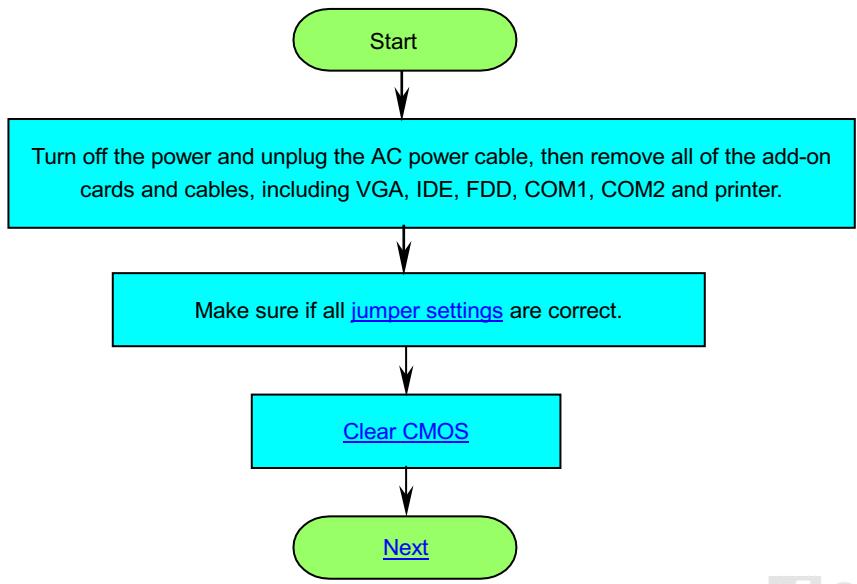
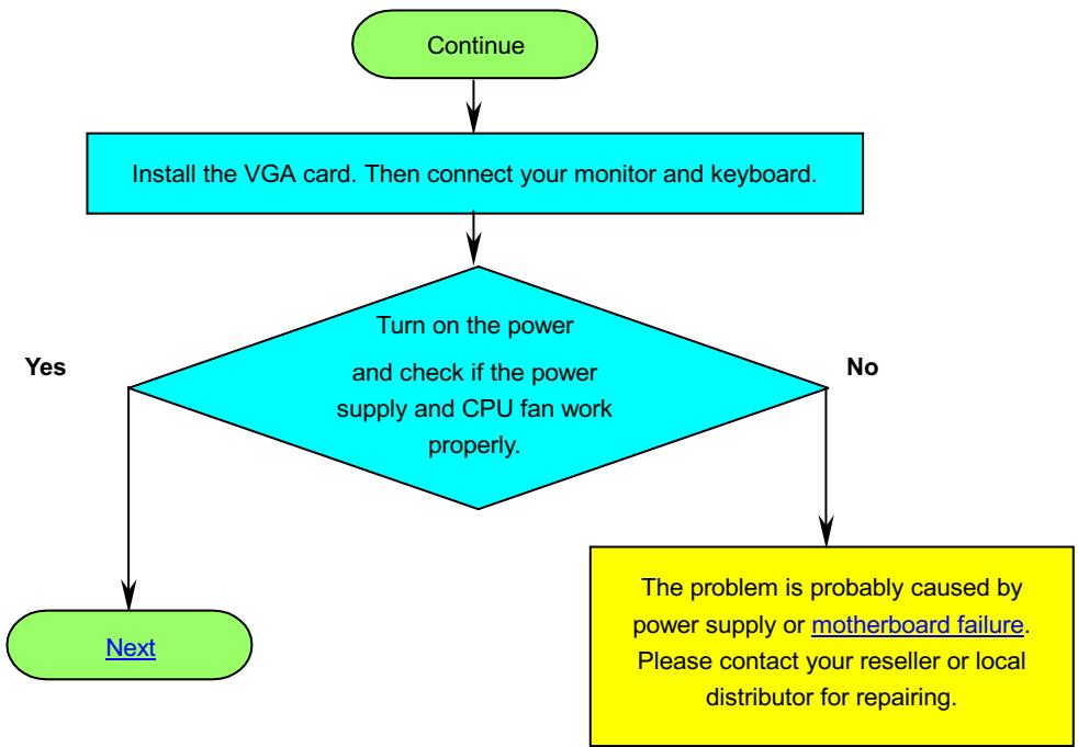
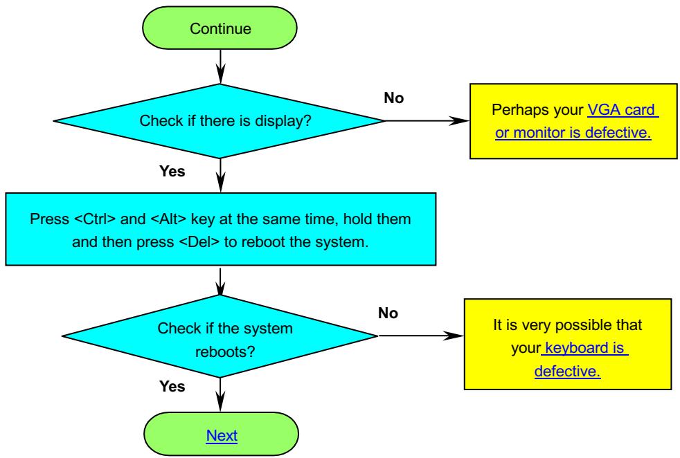
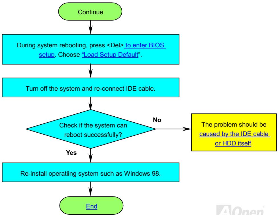

Technical Support
Dear Customer,
Thanks for choosing AOpen products. To provide the best and fastest service to our customer is our first priority. However, we receive numerous emails and phone-calls worldwide everyday, it is very hard for us to serve everyone on time. We recommend you follow the procedures below and seek help before contact us. With your help, we can then continue to provide the best quality service to more customers.
Thanks very much for your understanding!
AOpen Technical Supporting Team

Online Manual: Please check the manual carefully and make sure the jumper settings and installation procedure are correct.
http://www.aopen.com.tw/tech/download/manual/default.htm

Test Report: We recommend to choose board/card/device from the compatibility test reports for assembling your PC.
http://www.aopen.com.tw/tech/report/default.htm

FAQ: The latest FAQ (Frequently Asked Questions) may contain a solution to your problem.
http://www.aopen.com.tw/tech/faq/default.htm

Download Software: Check out this table to get the latest updated BIOS/utility and drivers.
http://www.aopen.com.tw/tech/download/default.htm

News Group: Your problem probably had been answered by our support engineer or professional users on the news group.
http://www.aopen.com.tw/tech/newsgrp/default.htm

Contact Distributors/Resellers: We sell our products through resellers and integrators. They should know your system configuration very well and should be able to solve your problem more efficiently than us. After all, their attitude of service is an important reference for you if next time you want to buy something else from them.

Contact Us: Please prepare detail system configuration and error symptom before contacting us. The part number, serial number and BIOS version are also very helpful.
Part Number and Serial Number
The Part Number and Serial number are printed on bar code label. You can find this bar code label on the outside packing, on ISA/CPU slot or on component side of PCB. For example:

P/N: 91.88110.201 is part number, S/N: 91949378KN73 is serial number
Model name and BIOS version
Model name and BIOS version can be found on upper left corner of first boot screen (POST screen). For example:
AX34 Pro R1.20 Jan.04.2000 AOpen Inc.
Award Plug and Play BIOS Extension v1.0A
Copyright © 1998, Award Software, Inc.
AX34 Pro is model name of motherboard, R1.20 is BIOS version.
Web: http://www.aopen.com
Email : Send us email by going through the contact form below.
English http://www.aopen.com.tw/tech/contact/techusa.htm
Japanese http://aojoaopen.com.tw/tech/contact/techjo.htm
Chinese http://w3.aopen.com.tw/tech/contact/techtw.htm
German http://www.aopencom.de/tech/contact/techde.htm
Simplified Chinese http://www.aopen.com.cn/tech/contact/techcn.htm
TEL:
USA 650-827-9688
Netherlands +31 73-645-9516
China (86) 755-375-3013
Taiwan (886) 2-2696-1333
Germany +49 (0) 2102-157-700
- AX34 Pro
- Online Manual
- What's in this manual
- AX34 Pro 1
- Hardware 14
- Driver and Utility 62
- AWARD BIOS 79
- Overclocking 146
- Glossary 149
- Troubleshooting 160
- Technical Support. 164
- Before You Start
- Quick Installation Procedure
- Hardware
- JP14 Clear CMOS
- CPU Socket
- CPU and Housing Fan Connector
- CPU Jumper-less Design
- Full-range Adjustable CPU Core Voltage
- Setting CPU Frequency
- JP29/JP23 FSB/PCI Clock Ratio
- JP33/JP32 Select CPU Type
- JP33/JP32
- DIMM Socket
- RAM Power LED
- Front Panel Connector
- ATX Power Connector
- AC Power Auto Recovery
- IDE and Floppy Connector
- IrDA Connector
- WOM (Zero Voltage Wake on Modem)
- WOM by External BOX Modem
- WOM by Internal Modem Card
- WOL (Wake on LAN)
- 4X AGP (Accelerated Graphic Port)
- AMR (Audio/Modem Riser)
- PC99 Color Coded Back Panel
- Support 4 USB Ports
- JP12 Enable/Disable Onboard Sound
- CD Audio Connector
- Modem Audio Connector
- MODEM-CN
- Video_Audio_IN Connector
- Battery-less and Long Life Design
- Over-current Protection
- Hardware Monitoring
- Resettable Fuse
- JP30 Die-Hard BIOS (100% Virus Protection)
- External Controller for DIE-HARD BIOS
- Year 2000 (Y2K)
- 2200uF Low ESR Capacitor
- Layout (Frequency Isolation Wall)
- 24K Gold Heatsink
- Driver and Utility
- Autorun Menu from Bonus CD Disc
- Installing Windows 95
- Installing Windows 98
- Installing Windows 98 SE & Windows2000
- Installing VIA 4 in 1 Driver
- Installing Onboard Sound Driver
- Installing Hardware Monitoring Utility
- ACPI Suspend to Hard Drive
- System Requirement
- Fresh installation of Windows 98 on a new system
- Changing from APM to ACPI (Windows 98 only)
- Run "Regedit.exe"
- Changing from ACPI to APM
- ACPI Suspend to RAM (STR)
- When go into Suspend:
- When power-on next time:
- Procedures
- AWARD BIOS
- Enter BIOS Setup
- Change Language
- Standard CMOS Setup
- Standard CMOS Setup > Date (mm:dd:yy)
- Standard CMOS Setup > Time (hh:mm:ss)
- Type
- Mode
- Standard CMOS Setup > Drive A
- Standard CMOS Setup > Drive B
- Drive A
- Standard CMOS Setup > Video
- Video
- Standard CMOS Setup > Halt On
- Halt On
- BIOS Features Setup
- BIOS Features Setup > Virus Warning
- Virus Warning
- !WARNING !
- BIOS Features Setup > External Cache
- External Cache
- BIOS Features Setup > CPU L2 Cache ECC Checking
- CPU L2 Cache ECC
- Checking
- BIOS Features Setup > Processor Number Feature
- Processor Number
- Feature
- BIOS Features Setup > Quick Power On Self Test
- Quick Power on Self
- Test
- BIOS Features Setup > Boot From LAN First
- Boot From LAN
- First
- BIOS Features Setup > Boot Sequence
- Boot Sequence
- BIOS Features Setup > Swap Floppy Drive
- Swap Floppy Drive
- BIOS Features Setup > Boot Up Floppy Seek
- Boot Up Floppy
- Seek
- BIOS Features Setup > Boot Up NumLock Status
- Boot Up NumLock
- Status
- BIOS Features Setup > Memory Parity/ECC Check
- Memory Parity/ECC
- Check
- BIOS Features Setup > Typematic Rate Setting
- Typematic Rate
- Setting
- BIOS Features Setup > Typematic Rate (Chars/Sec)
- BIOS Features Setup > Typematic Delay (Msec)
- Typematic Delay
- BIOS Features Setup > Security Option
- Security Option
- BIOS Features Setup > PCI/VGA Palette Snoop
- PCI/VGA Palette
- Snoop
- BIOS Features Setup > OS Select for DRAM > 64MB
- OS Select for DRAM
- BIOS Features Setup > Show Logo On Screen
- Show Logo On
- Screen
- BIOS Features Setup > Video BIOS Shadow
- Video BIOS Shadow
- C8000-CBFFF
- Shadow
- Chipset Features Setup
- Bank 0/1 DRAM
- Timing
- Chipset Features Setup > SDRAM CAS Latency
- SDRAM CAS Latency
- Chipset Features Setup > DRAM Clock
- DRAMClock
- Chipset Features Setup > Memory Hole At 15M-16M
- Memory Hole At
- Chipset Features Setup > Fast R-W Turn Around
- Fast R-W Turn
- Chipset Features Setup > System BIOS Cacheable
- System BIOS
- Chipset Features Setup > Video RAM Cacheable
- Video RAM Cacheable
- Chipset Features Setup > AGP Mode
- AGP Mode
- Chipset Features Setup > AGP Aperture Size
- AGP Aperture Size
- Chipset Features Setup > CPU Micro Codes
- CPU Micro Codes
- Chipset Features Setup > Clock Spread Spectrum
- Clock Spread Spectrum
- Chipset Features Setup > CPU Voltage Detected
- CPU Voltage Detected
- Chipset Features Setup > CPU Voltage Setting
- CPU Voltage Setting
- Chipset Features Setup > CPU Speed Detected
- CPU Speed Detected
- Chipset Features Setup > CPU Clock Frequency
- CPU Clock Frequency
- Chipset Features Setup > CPU Clock Ratio
- CPU Clock Ratio
- Chipset Features Setup > Setup CPU Speed
- Power Management Setup
- Power Management Setup > ACPI Function
- ACPI Function
- Power Management Setup > Power Management
- Power Management
- Power Management Setup > PM Controlled by APM
- PM Controlled by APM
- Power Management Setup > Video Off Method
- Video Off Method
- Power Management Setup > ACPI Suspend Type
- ACPI Suspend Type
- Power Management Setup > Standby Mode
- Standby Mode
- Power Management Setup > Suspend Mode
- Suspend Mode
- Power Management Setup > HDD Power Down
- HDD Power Down
- Power Management Setup > Soft-Off by PWRBTN
- Soft-Off by PWRBTN
- Power Management Setup > Wake On PCI Card
- Wake On PCI Card
- Power Management Setup > Wake On Modem
- Wake On Resume
- Power Management Setup > Wake On LAN
- Wake On LAN
- Power Management Setup > Wake On RTC Timer
- Wake On RTC Timer
- Power Management Setup > Date (of Month)
- Date (of Month)
- Power Management Setup > Timer (hh: mm: ss)
- Timer (hh: mm: ss)
- VGA
- Power Management Setup > AC PWR Auto Recovery
- AC PWR Auto
- Recovery
- Power Management Setup > Primary INTR
- Primary INTR
- IRQ 3 (COM 2)
- PNP/PCI Configuration Setup
- PNP/PCI Configuration > PNP OS Installed
- PNP OS Installed
- PNP/PCI Configuration > Resources Controlled By
- Resources Controlled
- IRQ 3 assigned to
- PNP/PCI Configuration > CPU to PCI Write Buffer
- PNP/PCI Configuration > PCI Dynamic Bursting
- PCI Dynamic Bursting
- PNP/PCI Configuration > PCI Master 0 WS Write
- PCI Master 0 WS
- Write
- PNP/PCI Configuration > PCI Delay Transaction
- PCI Delay Transaction
- PNP/PCI Configuration > PCI#2 Access #1 Retry
- PCI#2 Access #1
- Retry
- PNP/PCI Configuration > AGP Master 1 WS Write
- AGP Master 1 WS
- PNP/PCI Configuration > AGP Master 1 WS Read
- Read
- PNP/PCI Configuration > Assign IRQ for USB
- Assign IRQ for USB
- PNP/PCI Configuration > Assign IRQ for VGA
- Assign IRQ for VGA
- PNP/PCI Configuration > Modem Use IRQ
- Modem Use IRQ
- Slot1 IRQ No.
- Load Setup Defaults
- Load Turbo Defaults
- Integrated Peripherals
- OnChip Primary IDE
- Integrated Peripherals > IDE Prefetch Mode
- IDE Prefetch Mode
- Integrated Peripherals > IDE HDD Block Mode
- IDE HDD Block Mode
- Primary Master PIO
- Primary Master UDMA
- Integrated Peripherals > Init Display First
- Init Display First
- Integrated Peripherals > OnChip Sound
- OnChip Sound
- Integrated Peripherals > OnChip Legacy Audio
- OnChip Legacy Audio
- Integrated Peripherals > Sound I/O Base Address
- Sound I/O Base
- Address
- Integrated Peripherals > Sound IRQ Select
- Sound IRQ Select
- Integrated Peripherals > Sound DMA Select
- Sound DMA Select
- Integrated Peripherals > MPU-401 I/O Address
- MPU-401 I/O Address
- Integrated Peripherals > Onboard FDD Controller
- Onboard FDD
- Controller
- Integrated Peripherals > Onboard Serial Port 1
- Integrated Peripherals > Onboard Serial Port 2
- Onboard Serial Port 1
- Integrated Peripherals > UART 2 Mode
- UART 2 Mode
- Standard
- HPSIR
- ASKIR
- Integrated Peripherals > IR Function Duplex
- IR Function Duplex
- Integrated Peripherals > RxD, TxD Active
- RxD, TxD Active
- Integrated Peripherals > Onboard Parallel Port
- Onboard Parallel Port
- Integrated Peripherals > Onboard Parallel Mode
- Onboard Parallel
- SPP (Standard and Bidirection Parallel Port)
- EPP (Enhanced Parallel Port)
- ECP (Extended Parallel Port)
- Integrated Peripherals > ECP Mode Use DMA
- ECP Mode Use DMA
- Integrated Peripherals > Parallel Port EPP Type
- Parallel Port EPP
- Integrated Peripherals > OnChip USB
- OnChip USB
- Integrated Peripherals > USB Keyboard Support
- USB Keyboard
- Support
- Integrated Peripherals > AMR Function
- AMR Function
- Password Setting
- IDE HDD Auto Detection
- Save & Exit Setup
- Load EEPROM Default
- Save EEPROM Default
- Exit without Saving
- NCR SCSI BIOS and Drivers
- BIOS Upgrade
- DO NOT turn off the power during FLASH PROCESS.
- Overclocking
- VGA and HDD
- Glossary
- AC97
- ACPI (Advanced Configuration & Power Interface)
- AGP (Accelerated Graphic Port)
- AOpen Bonus Pack CD
- APM
- ATA/66
- ATA/100
- BIOS (Basic Input/Output System)
- Bus Master IDE (DMA mode)
- CODEC (Coding and Decoding)
- DIMM (Dual In Line Memory Module)
- ECC (Error Checking and Correction)
- EDO (Extended Data Output) Memory
- EEPROM (Electronic Erasable Programmable ROM)
- EPROM (Erasable Programmable ROM)
- FCC DoC (Declaration of Conformity)
- FC-PGA
- Flash ROM
- FSB (Front Side Bus) Clock
- I2C Bus
- P1394
- Parity Bit
- PBSRAM (Pipelined Burst SRAM)
- PC100 DIMM
- PC133 DIMM
- PDF Format
- PnP (Plug and Play)
- POST (Power-On Self Test)
- RDRAM (Rambus DRAM)
- RIMM
- SDRAM (Synchronous DRAM)
- SIMM (Single In Line Memory Module)
- SMBus (System Management Bus)
- SPD (Serial Presence Detect)
- Ultra DMA/33
- USB (Universal Serial Bus)
- ZIP file
- Troubleshooting
- Technical Support
- Part Number and Serial Number
- Model name and BIOS version
- TEL:
Marque : AOPEN
Modèle : AX34PRO
Catégorie : Carte mère