
46M1079 - Processor IBM - Free user manual and instructions
Find the device manual for free 46M1079 IBM in PDF.


| Product Type | Processor |
| Brand | IBM |
| Model | 46M1079 |
| Category | Processor |
| Socket Type | LGA 2011 |
| Core Count | 4 cores |
| Clock Speed | 2.0 GHz |
| Cache | 8 MB L3 |
| Thermal Design Power (TDP) | 95 W |
| Manufacturing Technology | 32 nm |
| Memory Support | DDR3 |
| Dimensions | 45 x 45 x 3.5 mm |
| Weight | 15 g |
| Power Consumption | 95 W |
| Cooling | Heat sink required |
| Functions | Data processing, multitasking, server workloads |
| Maintenance | Clean heat sink regularly, ensure proper thermal paste |
| Safety | Handle with ESD protection, avoid bending pins |
| Spare Parts | Not user-serviceable; replacement processor required |
| General Info | Designed for enterprise servers, reliable performance |
Frequently Asked Questions - 46M1079 IBM
User questions about 46M1079 IBM
0 question about this device. Answer the ones you know or ask your own.
Ask a new question about this device
Download the instructions for your Processor in PDF format for free! Find your manual 46M1079 - IBM and take your electronic device back in hand. On this page are published all the documents necessary for the use of your device. 46M1079 by IBM.
USER MANUAL 46M1079 IBM
Intel® Xeon® Processor 5500 Series
Thermal/ Mechanical Design Guide
March 2009
INFORMATION IN THIS DOCUMENT IS PROVIDED IN CONNECTION WITH INTEL® PRODUCTS. NO LICENSE, EXPRESS OR IMPLIED, BY ESTOPPEL OR OTHERWISE, TO ANY INTELLECTUAL PROPERTY RIGHTS IS GRANTED BY THIS DOCUMENT. EXCEPT AS PROVIDED IN INTEL'S TERMS AND CONDITIONS OF SALE FOR SUCH PRODUCTS, INTEL ASSUMES NO LIABILITY WHATSOEVER, AND INTEL DISCLAIMS ANY EXPRESS OR IMPLIED WARRANTY, RELATING TO SALE AND/OR USE OF INTEL PRODUCTS INCLUDING LIABILITY OR WARRANTIES RELATING TO FITNESS FOR A PARTICULAR PURPOSE, MERCHANTABILITY, OR INFRINGEMENT OF ANY PATENT, COPYRIGHT OR OTHER INTELLECTUAL PROPERTY RIGHT. Intel products are not intended for use in medical, life saving, or life sustaining applications.
Intel may make changes to specifications and product descriptions at any time, without notice.
Designers must not rely on the absence or characteristics of any features or instructions marked “reserved” or “undefined.” Intel reserves these for future definition and shall have no responsibility whatsoever for conflicts or incompatibilities arising from future changes to them.
The Intel® Xeon® processor 5500 series and LGA1366 socket may contain design defects or errors known as errata which may cause the product to deviate from published specifications. Current characterized errata are available on request.
Contact your local Intel sales office or your distributor to obtain the latest specifications and before placing your product order. Intel processor numbers are not a measure of performance. Processor numbers differentiate features within each processor family, not across different processor families. See http://www.intel.com/products/processor_number for details. Over time processor numbers will increment based on changes in clock, speed, cache, FSB, or other features, and increments are not intended to represent proportional or quantitative increases in any particular feature. Current roadmap processor number progression is not necessarily representative of future roadmaps. See www.intel.com/products/processor_number for details.
Intel® Turbo Boost Technology requires a PC with a processor with Intel Turbo Boost Technology capability. Intel Turbo Boost Technology performance varies depending on hardware, software and overall system configuration. Check with your PC manufacturer on whether your system delivers Intel Turbo Boost Technology. For more information, see www.intel.com.
Intel and the Intel logo are trademarks of Intel Corporation in the U.S and other countries.
* Other brands and names may be claimed as the property of others.
Copyright © 2009, Intel Corporation.
Contents
1 Introduction....9
1.1 References....10
1.2 Definition of Terms.... 10
2 LGA1366 Socket 13
2.1 Board Layout.... 15
2.2 Attachment to Motherboard 16
2.3 Socket Components.... 16
2.3.1 Socket Body Housing.... 16
2.3.2 Solder Balls 16
2.3.3 Contacts 17
2.3.4 Pick and Place Cover 17
2.4 Package Installation / Removal 18
2.4.1 Socket Standoffs and Package Seating Plane.... 18
2.5 Durability 19
2.6 Markings....19
2.7 Component Insertion Forces 19
2.8 Socket Size 19
2.9 LGA1366 Socket NCTF Solder Joints.... 20
3 Independent Loading Mechanism (ILM) 21
3.1 Design Concept....21
3.1.1 ILM Cover Assembly Design Overview 21
3.1.2 ILM Back Plate Design Overview 22
3.2 Assembly of ILM to a Motherboard.... 23
4 LGA1366 Socket and ILM Electrical, Mechanical, and Environmental Specifications. 27
4.1 Component Mass.... 27
4.2 Package/Socket Stackup Height 27
4.3 Socket Maximum Temperature....27
4.4 Loading Specifications.... 28
4.5 Electrical Requirements.... 28
4.6 Environmental Requirements 29
5 Thermal Solutions 31
5.1 Performance Targets.... 31
5.1.1 25.5 mm Tall Heatsink.... 33
5.2 Heat Pipe Considerations.... 34
5.3 Assembly 35
5.3.1 Thermal Interface Material (TIM) 36
5.4 Structural Considerations 36
5.5 Thermal Design 36
5.5.1 Thermal Characterization Parameter 36
5.5.2 Dual Thermal Profile 37
5.6 Thermal Features 38
5.6.1 Fan Speed Control.... 39
5.6.2 PECI Averaging and Catastrophic Thermal Management 40
5.6.3 Intel® Turbo Boost Technology 40
5.7 Thermal Guidance 40
5.7.1 Thermal Excursion Power for 95 W Processor 40
5.7.2 Thermal Excursion Power for 80 W Processor 41
5.7.3 Absolute Processor Temperature 41
intel®
6 Quality and Reliability Requirements 43
6.1 Test Conditions 43
6.2 Intel Reference Component Validation 45
6.2.1 Board Functional Test Sequence 45
6.2.2 Post-Test Pass Criteria....45
6.2.3 Recommended BIOS/Processor/Memory Test Procedures 46
6.3 Material and Recycling Requirements....46
A Component Suppliers....47
A.1 Intel Enabled Supplier Information....47
A.1.1 Intel Reference Thermal Solution 47
A.1.2 Intel Collaboration Thermal Solution....47
A.1.3 Alternative Thermal Solution 48
A.1.4 Socket and ILM Components 49
B Mechanical Drawings....51
C Socket Mechanical Drawings....79
D Heatsink Load Metrology....85
E Embedded Thermal Solutions....87
E.1 Performance Targets 87
E.2 Thermal Design Guidelines....88
E.2.1 NEBS Thermal Profile 88
E.2.2 Custom Heat Sinks For UP ATCA....89
E.3 Mechanical Drawings and Supplier Information 92
F Processor Installation Tool 97
Figures
1-1 Intel® Xeon® 5500 Platform Socket Stack 9
2-1 LGA1366 Socket with Pick and Place Cover Removed 13
2-2 LGA1366 Socket Contact Numbering (Top View of Socket) 14
2-3 LGA1366 Socket Land Pattern (Top View of Board) 15
2-4 Attachment to Motherboard 16
2-5 Pick and Place Cover 17
2-6 Package Installation / Removal Features....18
2-7 LGA1366 NCTF Solder Joints 20
3-1 ILM Cover Assembly 22
3-2 Back Plate 23
3-3 ILM Assembly 24
3-4 Pin1 and ILM Lever 25
4-1 Flow Chart of Knowledge-Based Reliability Evaluation Methodology ....30
5-1 1U Heatsink Performance Curves....32
5-2 TTV Die Size and Orientation....34
5-3 1U Reference Heatsink Assembly 35
5-4 Processor Thermal Characterization Parameter Relationships....37
5-5 Dual Thermal Profile 38
6-1 Example Thermal Cycle - Actual profile will vary 45
B-1 Board Keepin / Keepout Zones (Sheet 1 of 4)....52
B-2 Board Keepin / Keepout Zones (Sheet 2 of 4)....53
B-3 Board Keepin / Keepout Zones (Sheet 3 of 4)....54
B-4 Board Keepin / Keepout Zones (Sheet 4 of 4)....55
B-5 1U Reference Heatsink Assembly (Sheet 1 of 2) 56
B-6 1U Reference Heatsink Assembly (Sheet 2 of 2) 57
B-7 1U Reference Heatsink Fin and Base (Sheet 1 of 2) 58
B-8 1U Reference Heatsink Fin and Base (Sheet 2 of 2) 59
B-9 Heatsink Shoulder Screw (1U, 2U and Tower) 60
B-10Heatsink Compression Spring (1U, 2U and Tower)....61
B-11Heatsink Retaining Ring (1U, 2U and Tower) 62
B-12Heatsink Load Cup (1U, 2U and Tower)....63
B-132U Collaborative Heatsink Assembly (Sheet 1 of 2)....64
B-142U Collaborative Heatsink Assembly (Sheet 2 of 2)....65
B-152U Collaborative Heatsink Volumetric (Sheet 1 of 2) 66
B-162U Collaborative Heatsink Volumetric (Sheet 2 of 2) 67
B-17Tower Collaborative Heatsink Assembly (Sheet 1 of 2)....68
B-18Tower Collaborative Heatsink Assembly (Sheet 2 of 2)....69
B-19Tower Collaborative Heatsink Volumetric (Sheet 1 of 2) 70
B-20Tower Collaborative Heatsink Volumetric (Sheet 2 of 2) 71
B-211U Reference Heatsink Assembly with TIM (Sheet 1 of 2)....72
B-221U Reference Heatsink Assembly with TIM (Sheet 2 of 2)....73
B-232U Reference Heatsink Assembly with TIM (Sheet 1 of 2)....74
B-242U Reference Heatsink Assembly with TIM (Sheet 2 of 2)....75
B-25Tower Reference Heatsink Assembly with TIM (Sheet 1 of 2) 76
B-26Tower Reference Heatsink Assembly with TIM (Sheet 2 of 2) 77
C-1 Socket Mechanical Drawing (Sheet 1 of 4)....80
C-2 Socket Mechanical Drawing (Sheet 2 of 4)....81
C-3 Socket Mechanical Drawing (Sheet 3 of 4)....82
C-4 Socket Mechanical Drawing (Sheet 4 of 4)....83
D-1 Intel® Xeon® Processor 5500 Series Load Cell Fixture....86
E-1 ATCA Heatsink Performance Curves....88
E-2 NEBS Thermal Profile....89
E-3 UP ATCA Thermal Solution....90
E-4 UP ATCA System Layout 90
E-5 UP ATCA Heat Sink Drawing 91
E-6 ATCA Reference Heat Sink Assembly (Sheet 1 of 2)....93
E-7 ATCA Reference Heat Sink Assembly (Sheet 2 of 2)....94
E-8 ATCA Reference Heatsink Fin and Base (Sheet 1 of 2)....95
E-9 ATCA Reference Heatsink Fin and Base (Sheet 2 of 2)....96
F-1 Processor Installation Tool....98
intel®
Tables
1-1 Reference Documents 10
1-2 Terms and Descriptions....10
4-1 Socket Component Mass....27
4-2 1366-land Package and LGA1366 Socket Stackup Height 27
4-3 Socket and ILM Mechanical Specifications 28
4-4 Electrical Requirements for LGA1366 Socket 29
5-1 Boundary Conditions and Performance Targets 31
5-2 Performance Expectations for 25.5 mm Tall Heatsink....33
5-3 Fan Speed Control, TCONTROL and DTS Relationship 39
5-4 T CONTROL Guidance 39
6-1 Heatsink Test Conditions and Qualification Criteria 43
A-1 Suppliers for the Intel Reference Thermal Solution....47
A-2 Suppliers for the Intel Collaboration Thermal Solution 48
A-3 Suppliers for the Alternative Thermal Solution 48
A-4 LGA1366 Socket and ILM Components 49
B-1 Mechanical Drawing List 51
C-1 Mechanical Drawing List 79
E-1 Boundary Conditions and Performance Targets 87
E-2 Embedded Heatsink Component Suppliers 92
E-3 Mechanical Drawings List....92
Revision History
| Document Number Revision Number Description Revision Date | |||
| 321323 001 Public Release March 2009 | |||

1 Introduction
This document provides guidelines for the design of thermal and mechanical solutions for 2-socket server and 2-socket Workstation processors in the Intel® Xeon® 5500 Platform. The processors covered include those listed in the Intel® Xeon® Processor 5500 Series Datasheet, Volume 1 and the follow-on processors. The design guidelines apply to the follow-on processors in their current stage of development and are not expected to change as they mature. The components described in this document include:
- The processor thermal solution (heatsink) and associated retention hardware.
- The LGA1366 socket and the Independent Loading Mechanism (ILM) and back plate.
Processors in 1-socket Workstation platforms are covered in the Intel® Xeon® Processor 3500 Series Thermal/Mechanical Design Guide.
Figure 1-1. Intel® Xeon® 5500 Platform Socket Stack

The goals of this document are:
• To assist board and system thermal mechanical designers.
• To assist designers and suppliers of processor heatsinks.
Thermal profiles and other processor specifications are provided in the Datasheet.
1.1 References
Material and concepts available in the following documents may be beneficial when reading this document.
Table 1-1. Reference Documents
| Document Location Notes | ||
| European Blue Angel Recycling Standards 2 | ||
| Intel® Xeon® Processor 5500 Series Datasheet, Volume 1 321321 | 1 | |
| Intel® Xeon® Processor 5500 Series Mechanical Model 321326 1 | ||
| Intel® Xeon® Processor 5500 Series Thermal Model 321327 1 | ||
| Entry-level Electronics Bay Specification 3 |
Notes:
- Document numbers indicated in Location column are subject to change. See the appropriate Electronic Design Kit (EDK) for the most up-to-date Document number.
- Available at http://www.blauer-engel.de
- Available at http://ssiforum.oaktree.com/
1.2 Definition of Terms
Table 1-2. Terms and Descriptions (Sheet 1 of 2)
| Term Description | |
| Bypass | Bypass is the area between a passive heatsink and any object that can act to form a duct. For this example, it can be expressed as a dimension away from the outside dimension of the fins to the nearest surface. |
| DTS | Digital Thermal Sensor reports a relative die temperature as an offset from TCC activation temperature. |
| FSC | Fan Speed Control |
| IHS | Integrated Heat Spreader: a component of the processor package used to enhance the thermal performance of the package. Component thermal solutions interface with the processor at the IHS surface. |
| ILM | Independent Loading Mechanism provides the force needed to seat the 1366-LGA land package onto the socket contacts. |
| LGA1366 socket | The processor mates with the system board through this surface mount, 1366-contact socket. |
| PECI | The Platform Environment Control Interface (PECI) is a one-wire interface that provides a communication channel between Intel processor and chipset components to external monitoring devices. |
| _CA | Case-to-ambient thermal characterization parameter (psi). A measure of thermal solution performance using total package power. Defined as (T_CASE - T_LA) / Total Package Power. Heat source should always be specified for measurements. |
| _CS | Case-to-sink thermal characterization parameter. A measure of thermal interface material performance using total package power. Defined as (T_CASE - T_S) / Total Package Power. |
| _SA | Sink-to-ambient thermal characterization parameter. A measure of heatsink thermal performance using total package power. Defined as (T_S - T_LA) / Total Package Power. |
| T_CASE | The case temperature of the processor measured at the geometric center of the topside of the IHS. |
| T_CASE\_MAX | The maximum case temperature as specified in a component specification. |
| TCC | Thermal Control Circuit: Thermal monitor uses the TCC to reduce the die temperature by using clock modulation and/or operating frequency and input voltage adjustment when the die temperature is very near its operating limits. |
Table 1-2. Terms and Descriptions (Sheet 2 of 2)
| Term Description | |
| T_CONTROL | T_CONTROL is a static value below TCC activation used as a trigger point for fan speed control. |
| TDP Thermal Design | Power: Thermal solution should be designed to dissipate this target power level. TDP is not the maximum power that the processor can dissipate. |
| Thermal Monitor A power reduction feature designed to decrease temperature after the processor has reached its maximum operating temperature. | |
| Thermal Profile | Line that defines case temperature specification of a processor at a given power level. |
| TIM Thermal Interface Material: The thermally conductive compound between the heatsink and the processor case. This material fills the air gaps and voids, and enhances the transfer of the heat from the processor case to the heatsink. | |
| T_LA | The measured ambient temperature locally surrounding the processor. The ambient temperature should be measured just upstream of a passive heatsink or at the fan inlet for an active heatsink. |
| T_SA | The system ambient air temperature external to a system chassis. This temperature is usually measured at the chassis air inlets. |
| U | A unit of measure used to define server rack spacing height. 1U is equal to 1.75 in, 2U equals 3.50 in, etc. |
2 LGA1366 Socket
This chapter describes a surface mount, LGA (Land Grid Array) socket intended for processors in the Intel® Xeon® 5500 Platform. The socket provides I/O, power and ground contacts. The socket contains 1366 contacts arrayed about a cavity in the center of the socket with lead-free solder balls for surface mounting on the motherboard.
The socket has 1366 contacts with 1.016 mm X 1.016 mm pitch (X by Y) in a 43x41 grid array with 21x17 grid depopulation in the center of the array and selective depopulation elsewhere.
The socket must be compatible with the package (processor) and the Independent Loading Mechanism (ILM). The design includes a back plate which is integral to having a uniform load on the socket solder joints. Socket loading specifications are listed in Chapter 4.
Figure 2-1. LGA1366 Socket with Pick and Place Cover Removed

Figure 2-2. LGA1366 Socket Contact Numbering (Top View of Socket)

2.1 Board Layout
The land pattern for the LGA1366 socket is 40 mils X 40 mils (X by Y), and the pad size is 18 mils. Note that there is no round-off (conversion) error between socket pitch (1.016 mm) and board pitch (40 mil) as these values are equivalent.
Figure 2-3. LGA1366 Socket Land Pattern (Top View of Board)

scatter
| X | Y | Label | |---|---|---| | 1 | 2 | 1 | | 2 | 3 | 2 | | 3 | 4 | 3 | | 4 | 5 | 4 | | 5 | 6 | 5 | | 6 | 7 | 6 | | 7 | 8 | 7 | | 8 | 9 | 8 | | 9 | 10 | 9 | | 10 | 11 | 10 | | 11 | 12 | 11 | | 12 | 13 | 12 | | 13 | 14 | 13 | | 14 | 15 | 14 | | 15 | 16 | 15 | | 16 | 17 | 16 | | 17 | 18 | 17 | | 18 | 19 | 18 | | 19 | 20 | 19 | | 20 | 21 | 20 | | 21 | 22 | 21 | | 22 | 23 | 22 | | 23 | 24 | 23 | | 24 | 25 | 24 | | 25 | 26 | 25 | | 26 | 27 | 26 | | 27 | 28 | 27 | | 28 | 29 | 28 | | 29 | 30 | 29 | | 30 | 31 | 30 | | 31 | 32 | 31 | | AB | AB | AB | | AD | AD | AD | | AF | AF | AF | | AH | AH | AH | | AK | AK | AK | | AM | AM | AM | | AP | AP | AP | | AT | AT | AT | | AV | AV | AV | | AW | AW | AW BA | | AU | AU | AU AW BA | | AK | AK | AK | | AL | AL | AL AN AR AU AW BA | | AKH | AKH | AKH | | AKK | AKK | AKK | | AKLH | AKLH | AKLH | | AKM2.2 Attachment to Motherboard
The socket is attached to the motherboard by 1366 solder balls. There are no additional external methods (that is, screw, extra solder, adhesive, and so on) to attach the socket.
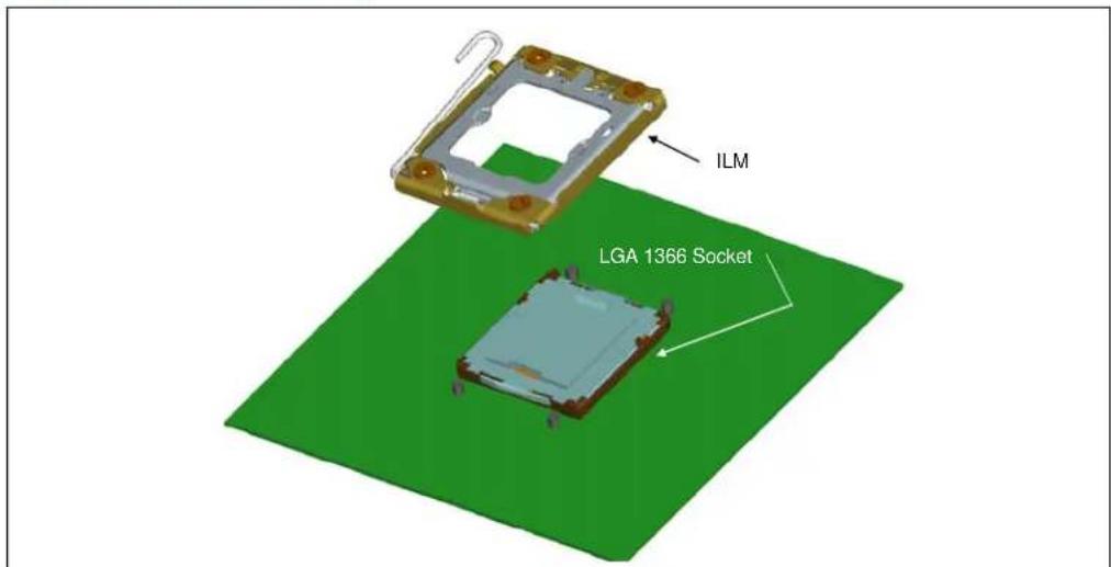
As indicated in Figure 2-4, the Independent Loading Mechanism (ILM) is not present during the attach (reflow) process.
Figure 2-4. Attachment to Motherboard
2.3 Socket Components
The socket has two main components, the socket body and Pick and Place (PnP) cover, and is delivered as a single integral assembly. Refer to Appendix C for detailed drawings.
2.3.1 Socket Body Housing
The housing material is thermoplastic or equivalent with UL 94 V-0 flame rating capable of withstanding 260 °C for 40 seconds (typical reflow/rework). The socket coefficient of thermal expansion (in the XY plane), and creep properties, must be such that the integrity of the socket is maintained for the conditions listed in the LGA1366 Socket Validation Reports.
The color of the housing will be dark as compared to the solder balls to provide the contrast needed for pick and place vision systems.
2.3.2 Solder Balls
A total of 1366 solder balls corresponding to the contacts are on the bottom of the socket for surface mounting with the motherboard.
The socket has the following solder ball material:
- Lead free SAC (SnAgCu) solder alloy with a silver (Ag) content between 3% and 4% and a melting temperature of approximately 217 °C. The alloy must be compatible with immersion silver (ImAg) motherboard surface finish and a SAC alloy solder paste.
The co-planarity (profile) and true position requirements are defined in Appendix C.
2.3.3 Contacts
Base material for the contacts is high strength copper alloy.
For the area on socket contacts where processor lands will mate, there is a 0.381 µm [15 µinches] minimum gold plating over 1.27 µm [50 µinches] minimum nickel underplate.
No contamination by solder in the contact area is allowed during solder reflow.
2.3.4 Pick and Place Cover
The cover provides a planar surface for vacuum pick up used to place components in the Surface Mount Technology (SMT) manufacturing line. The cover remains on the socket during reflow to help prevent contamination during reflow. The cover can withstand 260 °C for 40 seconds (typical reflow/rework profile) and the conditions listed in the LGA1366 Socket Validation Reports without degrading.
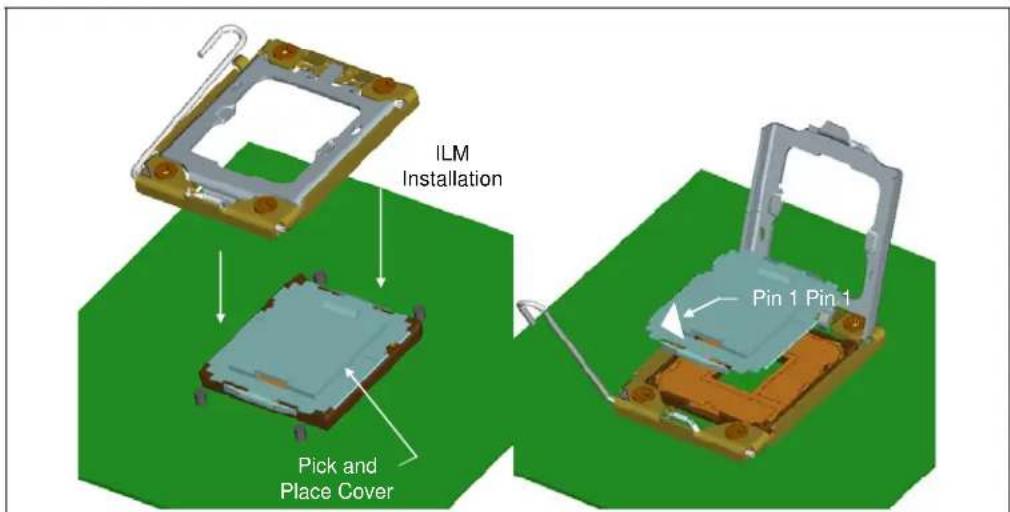
As indicated in Figure 2-5, the cover remains on the socket during ILM installation, and should remain on whenever possible to help prevent damage to the socket contacts.
Cover retention must be sufficient to support the socket weight during lifting, translation, and placement (board manufacturing), and during board and system shipping and handling.
The covers are designed to be interchangeable between socket suppliers. As indicated in Figure 2-5, a Pin1 indicator on the cover provides a visual reference for proper orientation with the socket.
Figure 2-5. Pick and Place Cover
2.4 Package Installation / Removal
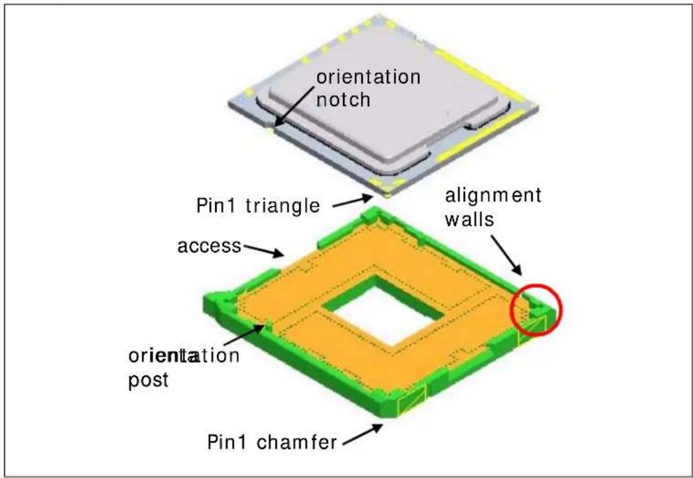
As indicated in Figure 2-6, access is provided to facilitate manual installation and removal of the package.
To assist in package orientation and alignment with the socket:
- The package Pin1 triangle and the socket Pin1 chamfer provide visual reference for proper orientation.
- The package substrate has orientation notches along two opposing edges of the package, offset from the centerline. The socket has two corresponding orientation posts to physically prevent mis-orientation of the package. These orientation features also provide initial rough alignment of package to socket.
- The socket has alignment walls at the four corners to provide final alignment of the package.
See Appendix F for information regarding a tool designed to provide mechanical assistance during processor installation and removal.
Figure 2-6. Package Installation / Removal Features
2.4.1 Socket Standoffs and Package Seating Plane
Standoffs on the bottom of the socket base establish the minimum socket height after solder reflow and are specified in Appendix C.
Similarly, a seating plane on the topside of the socket establishes the minimum package height. See Section 4.2 for the calculated IHS height above the motherboard.
2.5 Durability
The socket must withstand 30 cycles of processor insertion and removal. The max chain contact resistance from Table 4-4 must be met when mated in the 1st and 30th cycles.
The socket Pick and Place cover must withstand 15 cycles of insertion and removal.
2.6 Markings
There are three markings on the socket:
- LGA1366: Font type is Helvetica Bold - minimum 6 point (2.125 mm).
- Manufacturer's insignia (font size at supplier's discretion).
- Lot identification code (allows traceability of manufacturing date and location).
All markings must withstand 260 °C for 40 seconds (typical reflow/rework profile) without degrading, and must be visible after the socket is mounted on the motherboard.
LGA1366 and the manufacturer's insignia are molded or laser marked on the side wall.
2.7 Component Insertion Forces
Any actuation must meet or exceed SEMI S8-95 Safety Guidelines for Ergonomics/Human Factors Engineering of Semiconductor Manufacturing Equipment, example Table R2-7 (Maximum Grip Forces). The socket must be designed so that it requires no force to insert the package into the socket.
2.8 Socket Size
Socket information needed for motherboard design is given in Appendix C.
This information should be used in conjunction with the reference motherboard keep-out drawings provided in Appendix B to ensure compatibility with the reference thermal mechanical components.
2.9 LGA1366 Socket NCTF Solder Joints
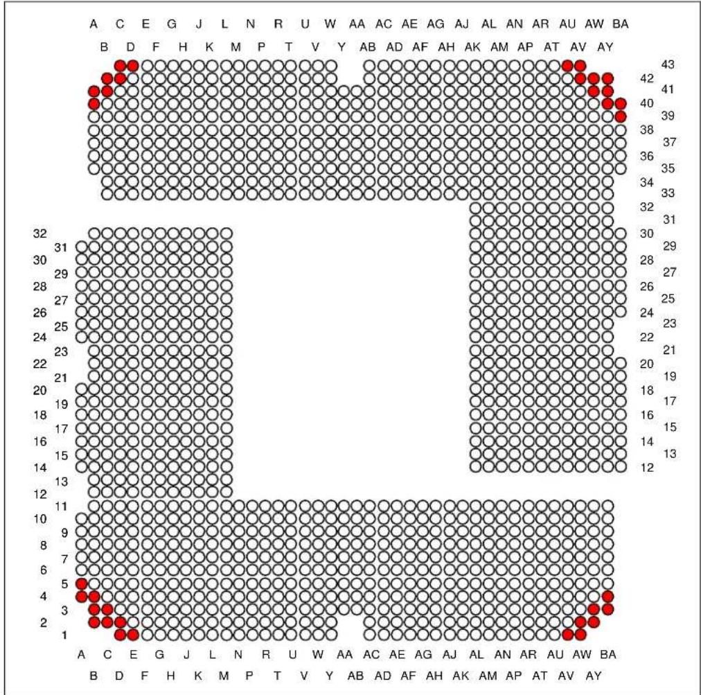
Intel has defined selected solder joints of the socket as non-critical to function (NCTF) for post environmental testing. The processor signals at NCTF locations are typically redundant ground or non-critical reserved, so the loss of the solder joint continuity at end of life conditions will not affect the overall product functionality. Figure 2-7 identifies the NCTF solder joints.
Figure 2-7. LGA1366 NCTF Solder Joints
scatter
| Letter | Value | |---|---| | A | 43 | | C | 42 | | E | 41 | | G | 40 | | J | 39 | | L | 38 | | N | 37 | | R | 36 | | U | 35 | | W | 34 | | AA | 33 | | AC | 32 | | AE | 31 | | AG | 30 | | AJ | 29 | | AL | 28 | | AN | 27 | | AR | 26 | | AU | 25 | | AW | 24 | | BA | 23 | | BY | 22 | | BY | 21 | | BY | 20 | | BY | 19 | | BY | 18 | | BY | 17 | | BY | 16 | | BY | 15 | | BY | 14 | | BY | 13 | | BY | 12 | | BY | 11 | | BY | 10 | | BY | 9 | | BY | 8 | | BY | 7 | | BY | 6 | | BY | 5 | | BY | 4 | | BY | 3 | | BY | 2 | | BY | 1 | A B C D E F H K M P T V Y AB AD AF AH AK AM AP AT AV AYNote: For platforms supporting the DP processor land C3 is CTF.
3 Independent Loading Mechanism (ILM)
The Independent Loading Mechanism (ILM) provides the force needed to seat the 1366-LGA land package onto the socket contacts. The ILM is physically separate from the socket body. The assembly of the ILM to the board is expected to occur after wave solder. The exact assembly location is dependent on manufacturing preference and test flow.
Note: The ILM has two critical functions: deliver the force to seat the processor onto the socket contacts and distribute the resulting compressive load evenly through the socket solder joints.
Note: The mechanical design of the ILM is integral to the overall functionality of the LGA1366 socket. Intel performs detailed studies on integration of processor package, socket and ILM as a system. These studies directly impact the design of the ILM. The Intel reference ILM will be "build to print" from Intel controlled drawings. Intel recommends using the Intel Reference ILM. Custom non-Intel ILM designs do not benefit from Intel's detailed studies and may not incorporate critical design parameters.
3.1 Design Concept
The ILM consists of two assemblies that will be procured as a set from the enabled vendors. These two components are ILM cover assembly and back plate.
3.1.1 ILM Cover Assembly Design Overview
The ILM Cover assembly consists of four major pieces: load lever, load plate, frame and the captive fasteners.
The load lever and load plate are stainless steel. The frame and fasteners are high carbon steel with appropriate plating. The fasteners are fabricated from a high carbon steel. The frame provides the hinge locations for the load lever and load plate.
The cover assembly design ensures that once assembled to the back plate and the load lever is closed, the only features touching the board are the captive fasteners. The nominal gap of the frame to the board is 1mm when the load plate is closed on the empty socket or when closed on the processor package.
When closed, the load plate applies two point loads onto the IHS at the "dimpled" features shown in Figure 3-1. The reaction force from closing the load plate is transmitted to the frame and through the captive fasteners to the back plate. Some of the load is passed through the socket body to the board inducing a slight compression on the solder joints.
Figure 3-1. ILM Cover Assembly

3.1.2 ILM Back Plate Design Overview
The unified back plate for 2-socket server and 2-socket Workstation products consists of a flat steel back plate with threaded studs for ILM attach, and internally threaded nuts for heatsink attach. The threaded studs have a smooth surface feature that provides alignment for the back plate to the motherboard for proper assembly of the ILM around the socket. A clearance hole is located at the center of the plate to allow access to test points and backside capacitors. An additional cut-out on two sides provides clearance for backside voltage regulator components. An insulator is pre-applied.
Back plates for processors in 1-socket Workstation platforms are covered in the Intel® Xeon® Processor 3500 Series Thermal/Mechanical Design Guide.
Figure 3-2. Back Plate

3.2 Assembly of ILM to a Motherboard
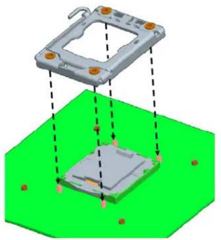
The ILM design allows a bottoms up assembly of the components to the board. In step 1, (see Figure 3-3), the back plate is placed in a fixture. Holes in the motherboard provide alignment to the threaded studs. In step 2, the ILM cover assembly is placed over the socket and threaded studs. Using a T20 Torx* driver fasten the ILM cover assembly to the back plate with the four captive fasteners. Torque to 8 ± 2 inch-pounds. The length of the threaded studs accommodate board thicknesses from 0.062" to 0.100".
Figure 3-3. ILM Assembly

natural_image
3D diagram of a microchip assembly with green and blue components, no text or symbols presentStep 1: With socket body reflowed on board, and back plate in fixture, align board holes to back plate studs.
natural_image
3D diagram of a mechanical component with dashed lines indicating alignment or assembly, no visible text or symbolsStep 2: With back plate against bottom of board, align ILM cover assembly to back plate studs.
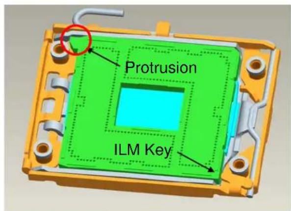
As indicated in Figure 3-4, socket protrusion and ILM key features prevent 180-degree rotation of ILM cover assembly with respect to the socket. The result is a specific Pin 1 orientation with respect to the ILM lever.
Figure 3-4. Pin1 and ILM Lever

4 LGA1366 Socket and ILM Electrical, Mechanical, and Environmental Specifications
This chapter describes the electrical, mechanical, and environmental specifications for the LGA1366 socket and the Independent Loading Mechanism.
4.1 Component Mass
Table 4-1. Socket Component Mass
| Component Mass | |
| Socket Body, Contacts and PnP Cover 15 gm | |
| ILM Cover 43 gm | |
| ILM Back Plate for dual processor server products 100 gm |
4.2 Package/ Socket Stackup Height
Table 4-2 provides the stackup height of a processor in the 1366-land LGA package and LGA1366 socket with the ILM closed and the processor fully seated in the socket.
Table 4-2. 1366-land Package and LGA1366 Socket Stackup Height
| Integrated Stackup Height (mm)From Top of Board to Top of IHS | 7.729 ± 0.282 mm |
Notes:
-
This data is provided for information only, and should be derived from: (a) the height of the socket seating plane above the motherboard after reflow, given in Appendix C, (b) the height of the package, from the package seating plane to the top of the IHS, and accounting for its nominal variation and tolerances that are given in the corresponding processor EMTS.
-
This value is a RSS calculation.
4.3 Socket Maximum Temperature
The power dissipated within the socket is a function of the current at the pin level and the effective pin resistance. To ensure socket long term reliability, Intel defines socket maximum temperature using a via on the underside of the motherboard. Exceeding the temperature guidance may result in socket body deformation, or increases in thermal and electrical resistance which can cause a thermal runaway and eventual electrical failure. The guidance for socket maximum temperature is listed below:
• Via temperature under socket < 96 °C
4.4 Loading Specifications
The socket will be tested against the conditions listed in the LGA1366 Socket Validation Reports with heatsink and the ILM attached, under the loading conditions outlined in this chapter.
Table 4-3 provides load specifications for the LGA1366 socket with the ILM installed. The maximum limits should not be exceeded during heatsink assembly, shipping conditions, or standard use condition. Exceeding these limits during test may result in component failure. The socket body should not be used as a mechanical reference or load-bearing surface for thermal solutions.
Table 4-3. Socket and ILM Mechanical Specifications
| Parameter Min Max Notes | |||
| Static compressive load from ILM cover to processor IHS | 470 N [106 lbf] 623 N [140 lbf] 3, 4 | ||
| Heatsink Static Compressive Load | 0 N [0 lbf] | 266 N [60 lbf] | 1, 2, 3 |
| Total Static Compressive Load (ILM plus Heatsink) | 470 N (106 lbf) 890 N (200 lbf) 3, 4 | ||
| Dynamic Compressive Load (with heatsink installed) | N/A | 890 N [200 lbf] | 1, 3, 5, 6 |
| Pick and Place Cover Insertion / Removal force | N/A | 10.2 N [2.3 lbf] | |
| Load Lever actuation force | N/A | 38.3 N [8.6 lbf] in the vertical direction10.2 N [2.3 lbf] in the lateral direction. |
Notes:
- These specifications apply to uniform compressive loading in a direction perpendicular to the IHS top surface.
- This is the minimum and maximum static force that can be applied by the heatsink and it's retention solution to maintain the heatsink to IHS interface. This does not imply the Intel reference TIM is validated to these limits.
- Loading limits are for the LGA1366 socket.
- This minimum limit defines the compressive force required to electrically seat the processor onto the socket contacts.
- Dynamic loading is defined as an 11 ms duration average load superimposed on the static load requirement.
- Test condition used a heatsink mass of 550gm [1.21 lb] with 50g acceleration measured at heatsink mass. The dynamic portion of this specification in the product application can have flexibility in specific values, but the ultimate product of mass times acceleration should not exceed this dynamic load.
4.5 Electrical Requirements
LGA1366 socket electrical requirements are measured from the socket-seating plane of the processor to the component side of the socket PCB to which it is attached. All specifications are maximum values (unless otherwise stated) for a single socket contact, but includes effects of adjacent contacts where indicated.
Table 4-4. Electrical Requirements for LGA1366 Socket
| Parameter Value Comment | ||
| Mated loop inductance, Loop | <3.9nH | The inductance calculated for two contacts, considering one forward conductor and one return conductor. These values must be satisfied at the worst-case height of the socket. |
| Mated partial mutual inductance, L | NA | The inductance on a contact due to any single neighboring contact. |
| Maximum mutual capacitance, C. | <1 pF | The capacitance between two contacts |
| Socket Average Contact Resistance (EOL) | 15.2 mΩ | The socket average contact resistance target is derived from average of every chain contact resistance for each part used in testing, with a chain contact resistance defined as the resistance of each chain minus resistance of shorting bars divided by number of lands in the daisy chain. The specification listed is at room temperature and has to be satisfied at all time.Socket Contact Resistance: The resistance of the socket contact, solderball, and interface resistance to the interposer land. |
| Max Individual Contact Resistance (EOL) | ≤100 mΩ | The specification listed is at room temperature and has to be satisfied at all time.Socket Contact Resistance: The resistance of the socket contact, solderball, and interface resistance to the interposer land; gaps included. |
| Bulk Resistance Increase | ≤3 mΩ | The bulk resistance increase per contact from 24 °C to 107 °C |
| Dielectric Withstand Voltage | 360 Volts RMS | |
| Insulation Resistance | 800 MΩ | |
4.6 Environmental Requirements
Design, including materials, shall be consistent with the manufacture of units that meet the following environmental reference points.
The reliability targets in this chapter are based on the expected field use environment for these products. The test sequence for new sockets will be developed using the knowledge-based reliability evaluation methodology, which is acceleration factor dependent. A simplified process flow of this methodology can be seen in Figure 4-1.
Figure 4-1. Flow Chart of Knowledge-Based Reliability Evaluation Methodology

flowchart
graph TD
    A["Establish the market/expected use environment for the technology"] --> B["Develop Speculative stress conditions based on historical data, content experts, and literature search"]
    B --> C["Perform stressing to validate accelerated stressing assumptions and determine acceleration factors"]
    C --> D["Freeze stressing requirements and perform additional data turns"]
A detailed description of this methodology can be found at:
ftp://download.intel.com/technology/itj/q32000/pdf/reliability.pdf.
5 Thermal Solutions
This section describes a 1U reference heatsink, design targets for 2U and Tower heatsinks, performance expectations for a 25.5 mm tall heatsink, and thermal design guidelines for Intel® Xeon® Processor 5500 Series and the follow-on processors.
5.1 Performance Targets
Table 5-1 provides boundary conditions and performance targets for 1U, 2U and Tower heatsinks. These values are used to generate processor thermal specifications and to provide guidance for heatsink design.
Table 5-1. Boundary Conditions and Performance Targets
| Parameter Value | |||||
| Altitude, system ambient temp | Sea level, 35°C | ||||
| TDP 60W 80W 95W, Profile B 95W, Profile A 130W, WS | 9 | ||||
| T_LA^1 | 49°C | 49°C | 49°C | 55°C | 40°C |
| Ψ_CA^2 | 0.335°C/W 0.336 | °C/W 0.337 | °C/W 0.201 | °C/W 0.201 | °C/W |
| Airflow3 | 9.7 CFM @ 0.20" dP | 9.7 CFM @ 0.20" dP | 9.7 CFM @ 0.20" dP | 30 CFM @ 0.205" dP | 30 CFM @ 0.205" dP |
| System height (form factor)4 | 1U (EEB) | 1U (EEB) | 1U (EEB)5 | 2U (EEB) | Pedestal (EEB) |
| Heatsink volumetric | 90 x 90 x 27mm (1U)6 | 90 x 90 x 64mm (2U)6,7 | 90 x 90 x 99mm (Tower)6 | ||
| Heatsink technology8 | Cu base, Al fins | Cu/Al base, Al fins with heatpipes | |||
Notes:
- Local ambient temperature of the air entering the heatsink.
- Max target (mean + 3 sigma + offset) for thermal characterization parameter (Section 5.5.1).
- Airflow through the heatsink fins with zero bypass. Max target for pressure drop (dP) measured in inches H_2O .
-
Reference system configuration. Processor is downstream from memory in EEB (Entry-Level Electronics Bay). Ducting is utilized to direct airflow.
-
The 1U heatsink can also meet Profile B for the 95W processor in TEB (Thin Electronics Bay) under the following conditions: TLA = 40^ , CA = 0.275^ / W , airflow = 16 CFM @ 0.344^ (these TEB values are not used to generate processor thermal specifications). Processor is not downstream from memory in TEB. Ducting is utilized to direct airflow.
-
Dimensions of heatsink do not include socket or processor.
-
The 2U heatsink height (64mm) + socket/processor height (7.729 mm, Table 4-2) complies with 76.2 mm max height for EEB monoplanar boards (http://ssiforum.oaktree.com/).
-
Passive heatsinks. PCM45F thermal interface material.
-
WS = Workstation.
For 1U reference heatsink, see Appendix B for detailed drawings. Table 5-1 specifies _CA and pressure drop targets at 9.7 CFM. Figure 5-1 shows _CA and pressure drop for the 1U heatsink versus the airflow provided. Best-fit equations are provided to prevent errors associated with reading the graph.
Figure 5-1. 1U Heatsink Performance Curves

line
| Q_hs, CFM | Ψ_ca, C/W | ΔP, inch water | | --------- | --------- | -------------- | | 0 | 0.15 | 0.00 | | 10 | 0.30 | 0.40 | | 20 | 0.27 | 0.60 | | 30 | 0.24 | 0.70 | | 40 | 0.21 | 0.80 | | 50 | 0.20 | 0.90 |For 2U and Tower heatsink, see Appendix B for volumetric drawings. Table 5-1 specifies _CA and pressure drop targets at 30 CFM. At airflows other than 30 CFM, _CA and pressure drop will differ between suppliers as their heatpipe and fin geometries will vary.
5.1.1 25.5 mm Tall Heatsink
For the 25.5 mm tall heatsink, Table 5-2 provides guidance regarding performance expectations. These values are not used to generate processor thermal specifications.
Table 5-2. Performance Expectations for 25.5 mm Tall Heatsink
| Parameter Value | |||
| Altitude, system ambient temp | Sea level, 35°C | ||
| TDP 95W, Profile B | |||
| T_LA^1 | 50°C | 49°C | 40°C |
| Ψ_CA^2 | 0.287°C/W 0.337 | °C/W 0.275 | °C/W |
| Airflow3 | 13.3 CFM @ 0.334" dP | 10 CFM @ 0.210" dP | 16 CFM @ 0.354" dP |
| System height (form factor)4 | SSI blade | 1U (EEB) | 1U (TEB) |
| Heatsink volumetric | 90 x 90 x 25.5mm (1U)5 | ||
| Heatsink technology6 | Cu base, Al fins | ||
Notes:
-
Local ambient temperature of the air entering the heatsink.
-
Max target (mean + 3 sigma + offset) for thermal characterization parameter (Section 5.5.1).
-
Airflow through the heatsink fins with zero bypass. Max target for pressure drop (dP) measured in inches H2O.
-
Reference system configuration. Processor is downstream from memory in SSI blade and EEB (Entry-Level Electronics Bay), not in TEB (Thin Electronics Bay). Ducting is utilized to direct airflow.
-
Dimensions of heatsink do not include socket or processor. The 25.5 mm heatsink height + socket/processor height (7.729 mm, Table 4-2) complies with 33.5mm max height for SSI blade boards (http://ssiforum.oaktree.com/).
-
Passive heatsinks. Dow Corning TC-1996 thermal interface material.
5.2 Heat Pipe Considerations
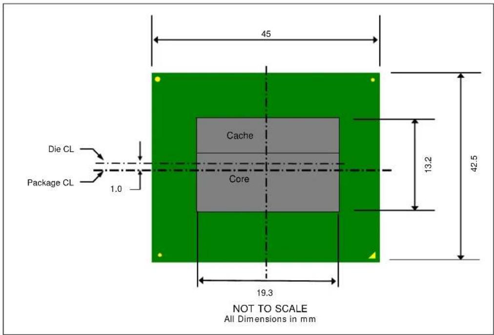
Figure 5-2 shows the orientation and position of the TTV die. The TTV die is sized and positioned similarly to the processor die.
Figure 5-2. TTV Die Size and Orientation
5.3 Assembly
Figure 5-3. 1U Reference Heatsink Assembly

The assembly process for the 1U reference heatsink begins with application of Honeywell PCM45F thermal interface material to improve conduction from the IHS. Tape and roll format is recommended. Pad size is 35 x 35mm, thickness is 0.25mm.
Next, position the heatsink such that the heatsink fins are parallel to system airflow. While lowering the heatsink onto the IHS, align the four captive screws of the heatsink to the four threaded nuts of the back plate.
Using a #2 Phillips driver, torque the four captive screws to 8 inch-pounds.
This assembly process is designed to produce a static load of 39 - 51 lbf, for 0.062" - 0.100" board thickness respectively. Honeywell PCM45F is expected to meet the performance targets in Table 5-1 from 30 - 60 lbf. From Table 4-3, the Heatsink Static Compressive Load of 0 - 60 lbf allows for designs that vary from the 1U reference heatsink. Example: A customer's unique heatsink with very little static load (as little as 0 lbf) is acceptable from a socket loading perspective as long as the T_CASE specification is met.
Compliance to Board Keepout Zones in Appendix B is assumed for this assembly process.
5.3.1 Thermal Interface Material (TIM)
TIM should be verified to be within its recommended shelf life before use.
Surfaces should be free of foreign materials prior to application of TIM.
Use isopropyl alcohol and a lint free cloth to remove old TIM before applying new TIM.
5.4 Structural Considerations
Mass of the 1U reference heatsink and the target mass for 2U and Tower heatsinks does not exceed 500 gm.
From Table 4-3, the Dynamic Compressive Load of 200 lbf max allows for designs that exceed 500 gm as long as the mathematical product does not exceed 200 lbf. Example: A heatsink of 2-lb mass (908 gm) x 50 g (acceleration) x 2.0 Dynamic Amplification Factor = 200 lbf. The Total Static Compressive Load (Table 4-3) should also be considered in dynamic assessments.
The heatsink limit of 500 gm and use of back plate have eliminated the need for Direct Chassis Attach retention (as used previously with the Intel® Xeon® processor 5000 sequence). Direct contact between back plate and chassis pan will help minimize board deflection during shock.
Placement of board-to-chassis mounting holes also impacts board deflection and resultant socket solder ball stress. Customers need to assess shock for their designs as their heatsink retention (back plate), heatsink mass and chassis mounting holes may vary.
5.5 Thermal Design
5.5.1 Thermal Characterization Parameter
The case-to-local ambient Thermal Characterization Parameter ( _CA ) is defined by:
$$ \text { Equation 5 - 1. } \Psi_ {\mathrm{CA}} = (T _ {\mathrm{CASE}} - T _ {\mathrm{LA}}) / \mathrm{TDP} $$
Where:
$$ \begin{array}{r l} \mathbf {T} _ {\text { CASE }} & = \text { Processor case temperature } (^ {\circ} \mathrm{C}). \text { For } \mathbf {T} \ & \quad \text { appropriate Datasheet. } \end{array} \quad \text { CASE specification see the } $$
$$ \mathbf {T} _ {\mathrm{LA}} = \text { Local ambient temperature in chassis at processor } (^ {\circ} \mathrm{C}). $$
$$ \begin{array}{l} \text { TDP } = \text { TDP (W) assumes all power dissipates through the integrated heat } \ \text { spreader. This inexact assumption is convenient for heatsink design. } \ \text { TTVs are often used to dissipate TDP. Correction offsets account for } \ \text { differences in temperature distribution between processor and TTV. } \end{array} $$
$$ \text { Equation 5 - 2. } \Psi_ {\mathrm{CA}} = \Psi_ {\mathrm{CS}} + \Psi_ {\mathrm{SA}} $$
Where:
$$ \begin{array}{r l} \Psi_ {C S} & = \text { Thermal characterization parameter of the TIM } (^ {\circ} C / W) \text { is dependent } \ & \text { on the thermal conductivity and thickness of the TIM. } \end{array} $$
$$ \begin{array}{r l} \Psi_ {\mathrm{SA}} & = \text { Thermal characterization parameter from heatsink - to - local ambient } \ & \quad (\mathrm {^ {\circ} C / W}) \text { is dependent on the thermal conductivity and geometry of the } \ & \text { heatsink and dependent on the air velocity through the heatsink fins. } \end{array} $$
Figure 5-4 illustrates the thermal characterization parameters.
Figure 5-4. Processor Thermal Characterization Parameter Relationships

5.5.2 Dual Thermal Profile
Processors that offer dual thermal profile are specified in the appropriate Datasheet.
Dual thermal profile helps mitigate limitations in volumetrically constrained form factors and allows trade-offs between heatsink cost and TCC activation risk. For heatsinks that comply to Profile B, yet do not comply to Profile A (1U heatsink in Figure 5-5), the processor has an increased probability of TCC activation and an associated measurable performance loss. Measurable performance loss is defined to be any degradation in processor performance greater than 1.5%. 1.5% is chosen as the baseline since run-to-run variation in a performance benchmark is typically between 1 and 2%.
Figure 5-5. Dual Thermal Profile

line
| POWER | T_CASE_MAX_B | T_CASE_MAX_A | Thermal Profile A | Thermal Profile B | |-------|--------------|--------------|-------------------|-------------------| | 0W | 40°C | 40°C | 40°C | 40°C | | TDP | ~45°C | ~45°C | ~38°C | ~38°C | | TCC | ~50°C | ~50°C | ~42°C | ~42°C |Compliance to Profile A ensures that no measurable performance loss will occur due to TCC activation. It is expected that TCC would only be activated for very brief periods of time when running a worst-case real world application in a worst-case thermal condition. A worst-case real world application is a commercially available, useful application which dissipates power above TDP for a thermally relevant timeframe. One example of a worst-case thermal condition is when the processor local ambient temperature is above the y-axis intercept for Profile A.
5.6 Thermal Features
More information regarding processor thermal features is contained in the appropriate Datasheet.
5.6.1 Fan Speed Control
There are many ways to implement fan speed control. Using processor ambient temperature (in addition to Digital Thermal Sensor) to scale fan speed can improve acoustics when DTS > T_CONTROL .
Table 5-3. Fan Speed Control, T CONTROL and DTS Relationship
| Condition FSC Scheme | |
| DTS ≤ T_CONTROL | FSC can adjust fan speed to maintain DTS ≤ T_CONTROL (low acoustic region). |
| DTS > T_CONTROL | FSC should adjust fan speed to keep T_CASE at or below the Thermal Profile specification (increased acoustic region). |
5.6.1.1 T CONTROL Guidance
Factory configured T_CONTROL values are available in the appropriate Dear Customer Letter or may be extracted by issuing a Mailbox or an RDMSR instruction. See the Intel® Xeon® Processor 5500 Series Datasheet, Volume 1 for more information.
Due to increased thermal headroom based on thermal characterization on the latest stepping of Intel® Xeon® Processor 5500 Series production processors, customers have the option to reduce T_CONTROL to values lower than the factory configured values.
In some situations, use of reduced T_CONTROL Guidance can reduce average fan power and improve acoustics. Implementation is optional. Alternately, the factory configured T_CONTROL values can still be used. There are no plans to change Intel's specification or the factory configured T_CONTROL values on individual processors.
To implement this guidance, customers must re-write code to set T_CONTROL to the reduced values provided in the table below.
Table 5-4. T CONTROL Guidance
| TDP | T_CONTROL Guidance | Comment |
| 95W -10 | Intel® Xeon® | Processor 5500 Series with 2.93 GHz Max Core Frequency |
| 95W -1 | Intel® Xeon® | Processor 5500 Series frequencies lower than 2.93 GHz |
| 80W -1 | Intel® Xeon® | Processor 5500 Series 2.53 GHz or lower, except Embedded (NEBS) |
| 60W -1 | Intel® Xeon® | Processor 5500 Series 2.26 GHz or lower, except Embedded (NEBS) |
Implementation of T_CONTROL Guidance above maintains Intel standards of reliability (based on modeling of the Intel Reference Design). Implementation of T_CONTROL of -1 may increase risk of throttling (Thermal Control Circuit activation). Increased TCC activation may or may not result in measurable performance loss.
Thermal Profile still applies. If PECI > = T_CONTROL Guidance, then the case temperature must meet the Thermal Profile.
T_CONTROL values for the follow-on processor are TBD but expected to be in the range of the factory configured T_CONTROL values for Intel® Xeon® Processor 5500 Series. Regardless of T_CONTROL values used in Intel® Xeon® Processor 5500 Series, BIOS needs to identify the processor type. For the follow-on processor, the fan speed control algorithm needs to use the follow-on processor's factory configured T_CONTROL values.
5.6.2 PECI Averaging and Catastrophic Thermal Management
By averaging DTS over PECI, thermal solution failure can be detected and a soft shutdown can be initiated to help prevent loss of data.
Thermal data is averaged over a rolling window of 256mS by default (X=8):
$$ \mathrm{AVG} _ {\mathrm{N}} = \mathrm{AVG} _ {\mathrm{N-1}} ^ {} (1 - 1 / 2 ^ {\mathrm{X}}) + \text { Temperature } ^ {} 1 / 2 ^ {\mathrm{X}} $$
Using a smaller averaging constant could cause premature detection of failure.
The Critical Temperature threshold generally triggers somewhere between PECI of -0.75 and -0.50. To avoid false shutdowns, initiate soft shutdown at -0.25.
Since customer designs, boundary conditions, and failure scenarios differ, above guidance should be tested in the customer's system to prevent loss of data during shutdown.
5.6.3 Intel® Turbo Boost Technology
Intel® Turbo Boost Technology (Intel® TBT) is a new feature available on certain processor SKUs that opportunistically, and automatically, allows the processor to run faster than the marked frequency if the part is operating below its power, temperature and current limits.
Heatsink performance (lower _CA as described in Section 5.5.1) is one of several factors that can impact the amount of Intel® TBT frequency benefit. Intel® TBT performance is also constrained by ICC, and VCC limits.
Increased IMON accuracy may provide more Intel® TBT benefit on TDP limited applications, as compared to lower _CA , as temperature is not typically the limiter for these workloads.
With Intel® TBT enabled, the processor may run more consistently at higher power levels (but still within TDP), and be more likely to operate above T_CONTROL , as compared to when Intel® TBT is disabled. This may result in higher acoustics.
With Intel® TBT enabled, processors with dual thermal profiles (described in Section 5.5.2, have greater potential for performance delta between Profile A and Profile B platforms, as compared to previous platforms.
5.7 Thermal Guidance
5.7.1 Thermal Excursion Power for 95 W Processor
Under fan failure or other anomalous thermal excursions, Tcase may exceed Thermal Profile B for a duration totaling less than 360 hours per year without affecting long term reliability (life) of the processor. For more typical thermal excursions, Thermal Monitor is expected to control the processor power level as long as conditions do not allow the Tcase to exceed the temperature at which Thermal Control Circuit (TCC) activation initially occurred. Under more severe anomalous thermal excursions when the processor temperature cannot be controlled at or below this Tcase level by TCC activation, then data integrity is not assured. At some higher threshold, THERMTRIP# will enable a shut down in an attempt to prevent permanent damage to the processor. Thermal Test Vehicle (TTV) may be used to check anomalous thermal excursion
compliance by ensuring that the processor Tcase value, as measured on the TTV, does not exceed Tcase_max_B at the anomalous power level for the environmental condition of interest. This anomalous power level is equal to 75% of the TDP limit.
5.7.2 Thermal Excursion Power for 80 W Processor
Under fan failure or other anomalous thermal excursions, Tcase may exceed the thermal profile for a duration totaling less than 360 hours per year without affecting long term reliability (life) of the processor. For more typical thermal excursions, Thermal Monitor is expected to control the processor power level as long as conditions do not allow the Tcase to exceed the temperature at which Thermal Control Circuit (TCC) activation initially occurred. Under more severe anomalous thermal excursions when the processor temperature cannot be controlled at or below this Tcase level by TCC activation, then data integrity is not assured. At some higher threshold, THERMTRIP# will enable a shut down in an attempt to prevent permanent damage to the processor. Thermal Test Vehicle (TTV) may be used to check anomalous thermal excursion compliance by ensuring that the processor Tcase value, as measured on the TTV, does not exceed Tcase_max at the anomalous power level for the environmental condition of interest. This anomalous power level is equal to 75% of the TDP limit.
5.7.3 Absolute Processor Temperature
Intel does not test any third party software that reports absolute processor temperature. As such, Intel cannot recommend the use of software that claims this capability. Since there is part-to-part variation in the TCC (thermal control circuit) activation temperature, use of software that reports absolute temperature can be misleading.
See the Intel® Xeon® Processor 5500 Series Datasheet, Volume 1 for details regarding use of IA32_TEMPERATURE_TARGET register to determine the minimum absolute temperature at which the TCC will be activated and PROCHOT# will be asserted.
6 Quality and Reliability Requirements
6.1 Test Conditions
The Test Conditions provided in Table 6-1 address processor heatsink failure mechanisms only. Test Conditions, Qualification and Visual Criteria vary by customer; Table 6-1 applies to Intel requirements.
Socket Test Conditions are provided in the LGA1366 Socket Validation Reports available from socket suppliers listed in Appendix A.
Table 6-1. Heatsink Test Conditions and Qualification Criteria (Sheet 1 of 2)
| Assessment Test | Condition Qualification Criteria | Min Sample Size | |
| 1) Humidity Non-operating, 500 hours, +85°C and 85% R.H. | No visual defects.As verified in wind tunnel:• M e aCA n 3s N offset not to exceed value in Table 5-1.• Pressure drop not to exceed value in Table 5-1. | 15 | |
| 2) Board-Level UnPackaged Shock | 50G+/-10%; 170+/-10% in/sec; 3 drops per face, 6 faces. | No damage to heatsink base or pipe.No visual defects.As verified in wind tunnel:• M e aCA n 2.54s + offset not to exceed value in Table 5-1.• Pressure drop not to exceed value in Table 5-1. | 15 |
| 3) Board-Level UnPackaged Vibration | 5 Hz @ 0.01 g2/Hz to 20 Hz @ 0.02 g2/Hz (slope up).20 Hz to 500 Hz @ 0.02 g2/Hz (flat).Input acceleration is 3.13 g RMS.10 minutes/axis for all 3 axes on all samples.Random control limit tolerance is ±3 dB. | No damage to heatsink base or pipe.No visual defects.As verified in wind tunnel:• M e aCA n 2.54s + offset not to exceed value in Table 5-1• Pressure drop not to exceed value in Table 5-1 | 15 |
| 4) First Article Inspection | Not Applicable | Meet all dimensions on 5 samples.Meet all CTF dimensions on 32 additional samples with 1.33 Cpk (mean + 4s).If samples are soft-tooled, a hard tool plan must be defined. | 37 |
| 5) Shipping Media: Packaged Shock | Drop height determined by weight and may vary by customer; Intel requirement in General Supplier Packaging Spec.10 drops (6 sides, 3 edges, 1 corner) | No visual defects | 1 box |
| 6) Shipping Media: Packaged Vibration | 0.015 g2/Hz @ 10-40 Hz, sloping to 0.0015 g2/Hz @ 500 Hz, 1.03 gRMS, 1 hour/axis for 3 axes | No visual defects | 1 box |
| 7) Gravitational Evaluation | Required for heatpipe designs.3 orientations (0°, +90°, -90°) | As verified in wind tunnel, mean _CA + 3s + offset not to exceed value in Table 5-1 | 15 |
Table 6-1. Heatsink Test Conditions and Qualification Criteria (Sheet 2 of 2)
| Assessment | Test Condition | Qualification Criteria | Min Sample Size |
| 8) Thermal Performance | Using 1U heatsink and 1U airflow from Table 5-1:1) TTV @ 95W (Profile B), Note 1. Using 2U heatsink and 2U airflow from Table 5-1:2) TTV @ 95W (Profile A), Note 1.3) TTV @ 80W.4) TTV @ 60W.Using Tower heatsink and Tower airflow from Table 5-1:5) TTV @ 130W, Note 1.6) TTV @ 95W (Profile A).7) TTV @ 80W.8) TTV @ 60W. | As verified in wind tunnel:1) mean _CA + 3s + offset not to exceed Table 5-1 value for 95W in 1U.2-4) mean _CA + 3s + offset not to exceed Table 5-1 value for 2U.5-8) mean _CA + 3s + offset not to exceed Table 5-1 value for Tower. | 5 heatsinks X 8 tests by supplier.Note 1: 30 heatsinks X 3 tests by Intel. |
| 9) Thermal Cycling Required for heatpipe designs.Temperature range at pipe in heatsink assembly: -25C to +100C for 500 cycles.Cycle time is 30 minutes per full cycle, divided into half cycle in hot zone and half in cold zone, with minimum 1min soak at each temperature extreme for each cycle.See Figure 6-1 for example profile. | As verified in wind tunnel:• M e aA n 3s N°offset not to exceed value in Table 5-1.• Pressure drop not to exceed value in Table 5-1. | 15 | |
| 10) Heat Pipe Burst Continuously raise oven temperature and record the burst/leak temperatures of fully assembled heatsinks | No failures at minimum of 300C @ 20 minutes | 32 pipes | |
| 11) Heatsink Mass Design Target < 500 g All samples < 550 g 30 | |||
| 12) Heatsink Load Design Targets:0.062" board = 38.7 ± 7.2 lbf (Fmin = 31.5 lbf).0.100" board = 51.4 ± 7.9 lbf (Fmax = 59.3 lbf). | No samples < 30 lbf on 0.062" board.5 highest load samples (from 0.062" test)< 60 lbf on 0.100" board | 30 | |
Figure 6-1. Example Thermal Cycle - Actual profile will vary

6.2 Intel Reference Component Validation
Intel tests reference components both individually and as an assembly on mechanical test boards, and assesses performance to the envelopes specified in previous sections by varying boundary conditions.
While component validation shows that a reference design is tenable for a limited range of conditions, customers need to assess their specific boundary conditions and perform reliability testing based on their use conditions.
Intel reference components are also used in board functional tests to assess performance for specific conditions.
6.2.1 Board Functional Test Sequence
Each test sequence should start with components (baseboard, heatsink assembly, and so on) that have not been previously submitted to any reliability testing.
The test sequence should always start with a visual inspection after assembly and BIOS/Processor/memory test. The stress test should be then followed by a visual inspection and then BIOS/Processor/memory test.
6.2.2 Post-Test Pass Criteria
The post-test pass criteria are:
-
No significant physical damage to the heatsink and retention hardware.
-
Heatsink remains seated and its bottom remains mated flat against the IHS surface. No visible gap between the heatsink base and processor IHS. No visible tilt of the heatsink with respect to the retention hardware.
- No signs of physical damage on baseboard surface due to impact of heatsink.
- No visible physical damage to the processor package.
- Successful BIOS/Processor/memory test.
- Thermal compliance testing to demonstrate that the case temperature specification can be met.
6.2.3 Recommended BIOS/ Processor/ Memory Test Procedures
This test is to ensure proper operation of the product before and after environmental stresses, with the thermal mechanical enabling components assembled. The test shall be conducted on a fully operational baseboard that has not been exposed to any battery of tests prior to the test being considered.
The testing setup should include the following components, properly assembled and/or connected:
- Appropriate system baseboard.
- Processor and memory.
- All enabling components, including socket and thermal solution parts.
The pass criterion is that the system under test shall successfully complete the checking of BIOS, basic processor functions and memory, without any errors.
6.3 Material and Recycling Requirements
Material shall be resistant to fungal growth. Examples of non-resistant materials include cellulose materials, animal and vegetable based adhesives, grease, oils, and many hydrocarbons. Synthetic materials such as PVC formulations, certain polyurethane compositions (for example, polyester and some polyethers), plastics which contain organic fillers of laminating materials, paints, and varnishes also are susceptible to fungal growth. If materials are not fungal growth resistant, then MIL-STD-810E, Method 508.4 must be performed to determine material performance.
Any plastic component exceeding 25 gm should be recyclable per the European Blue Angel recycling standards.
The following definitions apply to the use of the terms lead-free, Pb-free, and RoHS compliant.
Lead-free and Pb-free: Lead has not been intentionally added, but lead may still exist as an impurity below 1000 ppm.
RoHS compliant: Lead and other materials banned in RoHS Directive are either (1) below all applicable substance thresholds as proposed by the EU or (2) an approved/pending exemption applies.
Note: RoHS implementation details are not fully defined and may change.
A Component Suppliers
Various suppliers have developed support components for processors in the Intel® Xeon® 5500 Platform. These suppliers and components are listed as a convenience to customers. Intel does not guarantee quality, reliability, functionality or compatibility of these components. The supplier list and/or the components may be subject to change without notice. Customers are responsible for the thermal, mechanical, and environmental verification of the components with the supplier.
A.1 Intel Enabled Supplier Information
Performance targets for heatsinks are described in Section 5.1. Mechanical drawings are provided in Appendix B. Mechanical models are listed in Table 1-1. Heatsinks assemble to server back plate Table A-4.
A.1.1 Intel Reference Thermal Solution
The Intel reference thermal solutions has been verified to meet the criteria outlined in Table 6-1. Customers can purchase the Intel reference thermal solutions from the suppliers listed in Table A-1.
Table A-1. Suppliers for the Intel Reference Thermal Solution
| Assembly | Component | Description | Supplier PN | Supplier Contact Info |
| Assembly, Heat Sink, 1U | 1U URS Intel ReferenceHeatsink p/nE32409-001 | 27 mm 1U Aluminum Fin,Copper Base, includesTIM, 95W capable | FujikuraHSA-8078 Rev A | Fujikura AmericaYuji Yasudayuji@fujikura.com408-748-6991 |
| 1U URS SSI Blade ReferenceHeatsink p/nE39069-001 refersto E22056 Rev 02 +Snap Cover | 25.5mm 1U AluminumFin, Copper Base,includes TIM and SnapCover, 95W capable. | FujikuraHSA-8083C | Fujikura Taiwan BranchYao-Hsien Huangyeohsien@fujikuratw.com.tw886(2)8788-4959 |
A.1.2 Intel Collaboration Thermal Solution
The Intel collaboration thermal solutions are preliminary and may not be verified to meet the criteria outlined in Table 6-1. Customers can purchase the Intel collaboration thermal solutions from the suppliers listed in Table A-2.
Table A-2. Suppliers for the Intel Collaboration Thermal Solution
| Assembly Component Description Supplier PN Supplier Contact Info | ||||
| Assembly,Heatsink,Intel® Xeon® Processor 5500 Series, 2U | 2U URS HeatsinkIntel CollaborationHeatsink p/nE32410-001 | Supplier Designed Solution with Intel-specified retention, includes TIM, 95W capable | Foxconnpn 1A016500 | FoxconnWanchi Chen (worldwide)wanchi.chen@foxconn.com(408) 919-6135 |
| Assembly,Heatsink,Intel® Xeon® Processor 5500 Series, Pedestal | Tower URS HeatsinkIntel CollaborationHeatsink p/nE32412-001 | Supplier Designed Solution with Intel-specified retention, includes TIM, 130W capable | Chaun-Choung Technology Corp (CCI)pn 0007029401 | Chaun-Choung Technology Corp (CCI)Monica Chihmonica_chih@ccic.com.tw+886 (2) 2995-2666 x1131Harry Linhlinack@aol.com714 739-5797 |
A.1.3 Alternative Thermal Solution
The alternative thermal solutions are preliminary and are not verified by Intel to meet the criteria outlined in Table 6-1. Customers can purchase the alternative thermal solutions from the suppliers listed in Table A-3.
Table A-3. Suppliers for the Alternative Thermal Solution
| Assembly Component Description Supplier PN Supplier Contact Info | ||||
| Assembly, Heat Sink, 1U | 1U SSI Blade Alternative URS Heatsink | Supplier Designed Solution, Cu base, Al fins, 95W capable | TaiSol Corporation 1A1-9031000960-A | TaiSol Corporation Janice Chiu janice.chiu@taisol.com.tw +866-2-2656-2658 |
| Supplier Designed Solution, Cu base, Al fins, includes TIM, 95W capable | Thermaltake CL-P0484 | Thermaltake Sean Li sean@thermaltake.com.tw +886-2-26626501 EXT.235 | ||
| Assembly Heatsink, Intel® Xeon® Processor 5500 Series, 1U | 1U Alternative URS Heatsink | Supplier Designed Solution, Cu base, Al fins, includes TIM, 95W capable | CoolerMaster S1N-PJFCS-07-GP | CoolerMaster Isaac Chu isaac_chu@coolermaster.com.tw +886 2 32340050 x11182 |
| Supplier Designed Solution, Cu base, Al fins, includes TIM, 95W capable | Aavid Thermalloy 050073 | Aavid Thermalloy Chris Chapman chapman@aavid.com 603-223-1728 George Lee george.lee@aavid.com.tw +886 (2) 2698-9888 x603 | ||
Table A-3. Suppliers for the Alternative Thermal Solution
| Assembly Component Description Supplier PN Supplier Contact Info | ||||
| Assembly,Heatsink,Intel® Xeon® Processor 5500 Series, 2U | 2U Alternative URS Heatsink | Supplier Designed Solution,Aluminum base,Cu insert, Al fins,heatpipes,includes TIM, 95W capable | Asia Vital Components (AVC)SR40400001 | Asia Vital Components (AVC)David Chao david_chao@avc.com.tw+886 (2) 2299-6930 x7619 |
| Supplier Designed Solution, Cu base,Al fins, heatpipes,includes TIM, 95W capable | ThermaltakeCL-P0486 | ThermaltakeSean Li sean@thermaltake.com.tw+886-2-26626501 EXT.235 | ||
| Supplier Designed Solution, Cu base,Al fins, heatpipes,includes TIM, 95W capable | CoolerMasterS2N-PJMHS-07-GP | CoolerMasterIsaac Chu isaac_chu@coolermaster.com.tw+886 2 32340050 x11182 | ||
| Supplier Designed Solution, Cu base,Al fins, heatpipes,includes TIM, 95W capable | TaiSol Corporation1A0-9041000960-A | TaiSol CorporationJanice Chiu janice.chiu@taisol.com.tw+886-2-2656-3658 | ||
| Supplier Designed Solution,Aluminum Extrusion,includes TIM, 80W capable | Dynatron CorporationG520 | Dynatron CorporationIan Lee Ian@dynatron-corp.com510-498-8888 x137 | ||
| Assembly,Heatsink,Intel® Xeon® Processor 5500 Series, Tower | Tower Alternative URS Heatsink | Supplier Designed Solution, Al fins,heatpipes, 130W capable | TaiSol Corporation1A0-9051000960-A | TaiSol CorporationJanice Chiu janice.chiu@taisol.com.tw+886-2-2656-3658 |
| Supplier Designed Solution, Al fins,heatpipes, 130W capable | ThermaltakeCL-P0485 | ThermaltakeSean Li sean@thermaltake.com.tw+886-2-26626501 EXT.235 | ||
A.1.4 Socket and ILM Components
The LGA1366 Socket and ILM Components are described in Chapter 2 and Chapter 3, respectively. Socket mechanical drawings are provided in Appendix C. Mechanical models are listed in Table 1-1.
Table A-4. LGA1366 Socket and ILM Components
| Item Intel PN | Foxconn Tyco | ||
| ILM Cover Assembly D92428-002 PT | 44L12-4101 1939738-1 | ||
| Server Back Plate | D92433-002 | PT44P12-4101 | 1981467-1 |
| LGA1366 Socket | D86205-002 | PE136627-4371-01F | 1939737-1 |
| Supplier Contact Info | Julia Jiangjuliaj@foxconn.com408-919-6178 | Billy Hsiehbilly.hsieh@tycoelectronics.com+81 44 844 8292 | |
B Mechanical Drawings
Table B-1. Mechanical Drawing List
| Description Figure | |
| Board Keepin / Keepout Zones (Sheet 1 of 4) Figure B-1 | |
| Board Keepin / Keepout Zones (Sheet 2 of 4) Figure B-2 | |
| Board Keepin / Keepout Zones (Sheet 3 of 4) Figure B-3 | |
| Board Keepin / Keepout Zones (Sheet 4 of 4) Figure B-4 | |
| 1U Reference Heatsink Assembly (Sheet 1 of 2) Figure B-5 | |
| 1U Reference Heatsink Assembly (Sheet 2 of 2) Figure B-6 | |
| 1U Reference Heatsink Fin and Base (Sheet 1 of 2) Figure B-7 | |
| 1U Reference Heatsink Fin and Base (Sheet 2 of 2) Figure B-8 | |
| Heatsink Shoulder Screw (1U, 2U and Tower) Figure B-9 | |
| Heatsink Compression Spring (1U, 2U and Tower) Figure B-10 | |
| Heatsink Retaining Ring (1U, 2U and Tower) Figure B-11 | |
| Heatsink Load Cup (1U, 2U and Tower) Figure B-12 | |
| 2U Collaborative Heatsink Assembly (Sheet 1 of 2) Figure B-13 | |
| 2U Collaborative Heatsink Assembly (Sheet 2 of 2) Figure B-14 | |
| 2U Collaborative Heatsink Volumetric (Sheet 1 of 2) | Figure B-15 |
| 2U Collaborative Heatsink Volumetric (Sheet 2 of 2) | Figure B-16 |
| Tower Collaborative Heatsink Assembly (Sheet 1 of 2) | Figure B-17 |
| Tower Collaborative Heatsink Assembly (Sheet 2 of 2) | Figure B-18 |
| Tower Collaborative Heatsink Volumetric (Sheet 1 of 2) | Figure B-19 |
| Tower Collaborative Heatsink Volumetric (Sheet 2 of 2) | Figure B-20 |
| 1U Reference Heatsink Assembly with TIM (Sheet 1 of 2) | Figure B-21 |
| 1U Reference Heatsink Assembly with TIM (Sheet 2 of 2) | Figure B-22 |
| 2U Reference Heatsink Assembly with TIM (Sheet 1 of 2) | Figure B-23 |
| 2U Reference Heatsink Assembly with TIM (Sheet 2 of 2) | Figure B-24 |
| Tower Reference Heatsink Assembly with TIM (Sheet 1 of 2) | Figure B-25 |
| Tower Reference Heatsink Assembly with TIM (Sheet 2 of 2) | Figure B-26 |
Figure B-1. Board Keepin / Keepout Zones (Sheet 1 of 4)
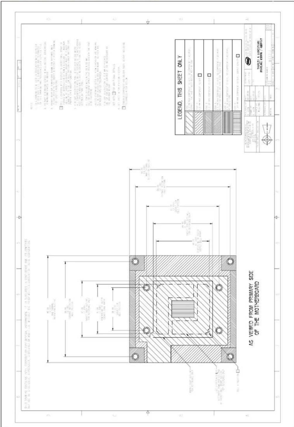
Figure B-2. Board Keepin / Keepout Zones (Sheet 2 of 4)
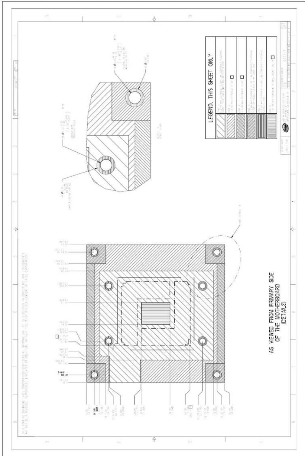
Figure B-3. Board Keepin / Keepout Zones (Sheet 3 of 4)

Figure B-4. Board Keepin / Keepout Zones (Sheet 4 of 4)
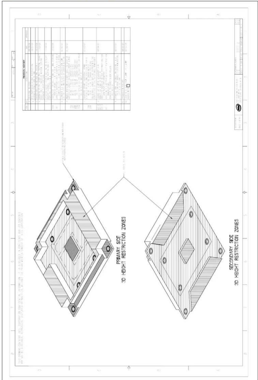
Figure B-5. 1U Reference Heatsink Assembly (Sheet 1 of 2)

Figure B-6. 1U Reference Heatsink Assembly (Sheet 2 of 2)
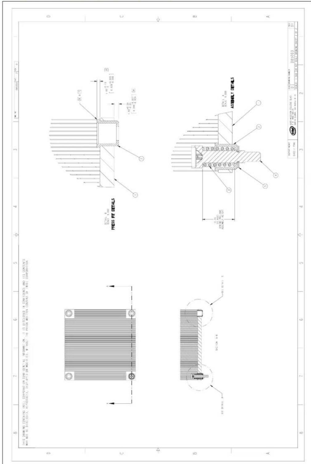
Figure B-7. 1U Reference Heatsink Fin and Base (Sheet 1 of 2)
![THIS DRAW NO CONTAINS INTEL CORPORATION CONFIDENTIAL INFORMATION IT IS DISCLOSED IN CONFISSIONS AND ITS CONTENTS MAY NOT BE DISCLOSED, REPRODUCED, DISPLAYED OR MODIFIED, WITHOUT THE PRIOR WRITTEN CONSENT OF INTEL CORPORATION. TOP VIEW A B C D ECE DETAIL 8 7 6 5 4 3 2 1 95.04 ± .25 [ Y 143] [ 90] 95.04 ± .25 [ Y 143] [ 90] 95.04 ± .25 [ Y 143] [ 90] 95.04 ± .25 [ Y 143] [ 90] 95.04 ± .25 [ Y 143] [ 90] 95.04 ± .25 [ X 143] [ 90] 95.04 ± .25 [ X 143] [ 90] 95.04 ± .25 [ X 143] [ 90] 95.04 ± .25 [ X 143] [ 90] 95.04 ± .25 [ X 143] [ 90] 90.04 ± .25 [ Y 143] [ 90] 90.04 ± .25 [ Y 143] [ 90] 90.04 ± .25 [ Y 143] [ 90] 90.04 ± .25 [ Y 143] [ 90] 90.04 ± .25 [ X 143] [ 90] 90.04 ± .25 [ X 143] [ 90] 90.04 ± .25 [ X 143] [ 90] 90.04 ± .25 [ X 143] [ 90] 90.04 ± .25 [ X 143] [ 90] 95.04 ± .25 [ Y 143] [ 90] 95.04 ± .25 [ Y 143] [ 90] 95.04 ± .25 [ Y 143] [ 90] 95.04 ± .25 [ Y 143] [ 90] 90.04 ± .25 [ Y 143] [ 90] 90.04 ± .25 [ Y 143] [ 90] 90.04 ± .25 [ Y 143] [ 90] 90.04 ± .25 [ X 8,8,8,8,8,8,8,8,8,8,8,8,8,8,8,8,8,8,8,8,8,8,8,8,8,8,8,8,8,8,8,8,8,8,8,8,8,8,8,8,8,8,8,8,8,8,8,8,8,8,8, TITLE: SHEET SENS. TITLE: SHEET ZONE. TITLE: SHEET ZONE. TITLE: SHEET ZONE. TITLE: SHEET ZONE. TITLE: SHEET ZONE. TITLE: SHEET ZONE. TITLE: SHEET ZONE. TITLE: SHEET ZONE. TITLE: SHEET ZONE. TITLE: SHEET ZONE. TITLE: SHEET ZONE. TITLE: SHEET ZONE. TITLE: SHEET ZONE. TITLE: SHEET ZONE. TITLE: SHEET ZONE. NOTE: 1. THIS DRAW NO TO BE USED IN CONJUNCTION WITH SUPPLIED TO BATHRASS FILED, ALL DIMENSIONS AND TOLERANCES ON THIS DRAW NO TEXT PROCEDURE OVER SUPPLIED FILED, TRIMINATE √ MAXIMUM STARS IN MIL-AL-MILLIERS, CORPORATION DIMENSIONS STARTED IN MINES, OFF CAN OF FOUNT ON FLOWERATION, ALL DIMENSION AND TOLERANCES FOR RANS (FIL) & (FIRE), EAST CORPIT, MAXIMUM STARS IN MIL-AL-MILLIERS, OFF CAN OF FOUNT ON FLOWERATION, ALL DIMENSION AND TOLERANCES FOR RANS (FIL) & (FIRE), EAST CORPIT, MAXIMUM STARS IN MIL-AL-MILLIERS, OFF CAN OF FOUNT ON FLOWERATION, ALL DIMENSION AND TOLERANCES FOR RANS (FIL) & (FIRE), EAST CORPIT, MAXIMUM STARS IN MIL-AL-MILLIERS, EAST CORPIT, MAXIMUM STARS IN MIL-AL-MILLIERS, EAST CORPIT, MAXIMUM STARS IN MIL-AL-MILLIERS, EAST CORPIT, MAXIMUM STARS IN MIL-AL-MILLIERS, EAST CORPIT, MAXIMUM STARS IN MIL-AL-MILLIERS, EAST CORPIT, MAXIMUM STARS IN MIL-AL-MILLIERS,\( \frac{1}{2} \) DIRECTION OF RESISTANCE OF AUMULATED AIR FOATS EAST CORPIT, MAXIMUM STARS IN MIL-AL-MILLIERS,\( \frac{1}{2} \) DIRECTION OF RESISTANCE OF AUMULATED AIR FOATS\(\frac{1}{2}\) DIRECTION OF RESISTANCE OF AUMULATED AIR FOATS\(\frac{1}{2}\) DIRECTION OF RESISTANCE OF AUMULATED AIR FOATS\(\frac{1}{2}\) EAST CORPIT, MAXIMUM STARS IN MIL-AL-MILLIERS,\( \frac{1}{2} \) DIRECTION OF RESISTANCE OF AUMULATED AIR FOATS\(\frac{1}{2}\) DIRECTION OF RESISTANCE OF AUMULATED AIR FOATS\(\frac{1}{2}\) EAST CORPIT, MAXIMUM STARS IN MIL-AL-MILLIERS,\( \frac{1}{2} \) DIRECTION OF RESISTANCE OF AUMULATED AIR FOATS\(\frac{1}{2}\) EAST CORPIT, MAXIMUM STARS IN MIL-AL-MILLIERS,\( \frac{1}{2} \) DIRECTION OF RESISTANCE OF AUMULATED AIR FOATS\(\frac{1}{2}\) EAST CORPIT, MAXIMUM STARS IN MIL-AL-MILLIERS,\( \underline{\underline{1}} \) DIRECTION OF RESISTANCE OF AUMULATED AIR FOATS\(\underline{\underline{1}}\) EAST CORPIT, MAXIMUM STARS IN MIL-AL-MILLIERS,\( \underline{\underline{1}} \) DIRECTION OF RESISTANCE OF AUMULATED AIR FOATS\(\underline{\underline{1}}\) EAST CORPIT, MAXIMUM STARS IN MIL-AL-MILLIERS,\( \underline{\underline{1}} \) DIRECTION OF RESISTANCE OF AUMULATED AIR FOATS\n\( \underline{\underline{1}} \) DIRECTION OF RESISTANCE OF AUMULATED AIR FOATS\n\( \underline{\underline{1}} \) DIRECTION OF RESISTANCE OF AUMULATED AIR FOATS\n\( \underline{\underline{1}} \) DIRECTION OF RESISTANCE OF AUMULATED AIR FOATS\n\( \underline{\underline{1}} \) DIRECTION OF RESISTANCE OF AUMULATED AIR FOATS\nHEAT SHAK, CU BASE, AL FINS. I.U. SIZE: SHEET NUMBER: D/90067 SCALE: T DE NOT SCALE DRAWING SHEET BY: Z](/content/2026/05/987880/images/c7b8271dd2fc8b116fa838a65dfba6bfa791028917a2fa34721fd72ff376d860.jpg)
Figure B-8. 1U Reference Heatsink Fin and Base (Sheet 2 of 2)
![THIS DRAWING CONTAINS INTEL CORPORATION CONFIDENTIAL INFORMATION. IT IS DISCLOSED IN CONFIDENCE AND ITS CONTENTS MAY NOT BE DISCLOSED. REPRODUCED. DISPLAYED ON MODIFIED, WITHOUT THE PRIOR WRITTEN CONSENT OR INTEL CORPORATION. D ① 2014-03-28 [0.249*0.000] [Φ]E:16.16.001[Φ][C] RIGHT C 2014-03-28 SECTION A-A NOT DETAIL 2 RIGHT B 2014-03-28 DETAIL B 2014-03-28 RIGHT C 2014-03-28 BOTTOM VIEW DESCRIPTION UNIT / FWH 2005 MISION CLOSE BLVD P.D. 104 HR 5 2005 CLARK CA 9992/499 SCALE: 1.567 GB NET SCALE DRAWING SHEET 2 OF 2 B A A B C D E F G H I J K L M N O P Q R S T U V W X Y Z A B C D E F G H I J K L U V W X Y Z A](/content/2026/05/987880/images/10f3391d61fe1dbae221ef5e55129d3380f6f299a250a9b15b8f2ae24aa35fc3.jpg)
Figure B-9. Heatsink Shoulder Screw (1U, 2U and Tower)
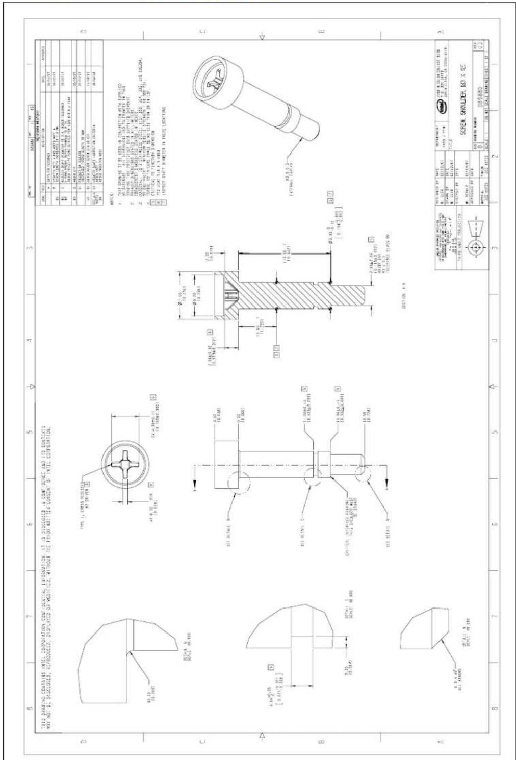
Figure B-10. Heatsink Compression Spring (1U, 2U and Tower)
![TH-S DRAWING CONTAINS INTEL CORPORATION CONFIDENTIAL INFORMATION. IT IS DISCLOSED IN CONFIDENCE AND ITS CONTENTS MAY NOT BE DISCLOSED, REPRODUCED, DIPLATED OR MODIFIED, WITHOUT THE PRIOR WRITTEN CONSENT OF INTEL CORPORATION. D C B A 8 7 6 5 4 3 2 1 0 0 0 0 0 0 0 0 0 0 0 0 0 0 0 0 0 0 0 0 0 0 0 0 0 0 0 0 0 0 0 0 0 0 0 0 0 0 0 0 0 0 0 0 0 0 0 0 0 0 1.5 6.112.34 [5] [6.112.34] [6.112.34] [6.112.34] [6.112.34] [6.112.34] [6.112.34] [6.112.34] [6.112.34] [6.112.34] [6.112.34] [6.112.35] [6.112.35] [6.112.35] [6.112.35] [6.112.35] [6.112.35] [6.112.35] [6.112.35] [6.112.35] [6.112.35] [6.112.36] [6.112.36] [6.112.36] [6.112.36] [6.112.36] [6.112.36] [6.112.36] [6.112.36] [6.112.36] [6.112.36] [6.112.37] [6.112.37] [6.112.37] [6.112.37] [6.112.37] [6.112.37] [6.112.37] [6.112.37] [6.112.37] [6.112.37] [6.112.38] [6.112.38] [6.112.38] [6.112.38] [6.112.38] [6.112.38] [6.112.38] [6.112.38] [6.112.38] [6.112.38] [6.112.39] [6.112.39] [6.112.39] [6.112.39] [6.112.39] [6.112.39] [6.112.39] [6.112.39] [6.112.39] [6.112.39] [6.112.38] [6.112.38] [6.112.38] [6.112.38] [6.112.38] [6.112.38] [6.112.38] [6.112.38] [6.112.38] [6.112.37] [6.112.37] [6.112.37] [6.112.37] [6.112.37] [6.112.37] [6.112.37] [6.112.37] [6.112 38] SOLIO HEIGHT FREE HEIGHT ECTION A A MATERIALS: COMPRESSION PRE-LOAD D89882 0](/content/2026/05/987880/images/ae3543cd772e378175d4cfcdda1dd553c9f95701790c5d21a903d15d2be01a6e.jpg)
Figure B-11. Heatsink Retaining Ring (1U, 2U and Tower)
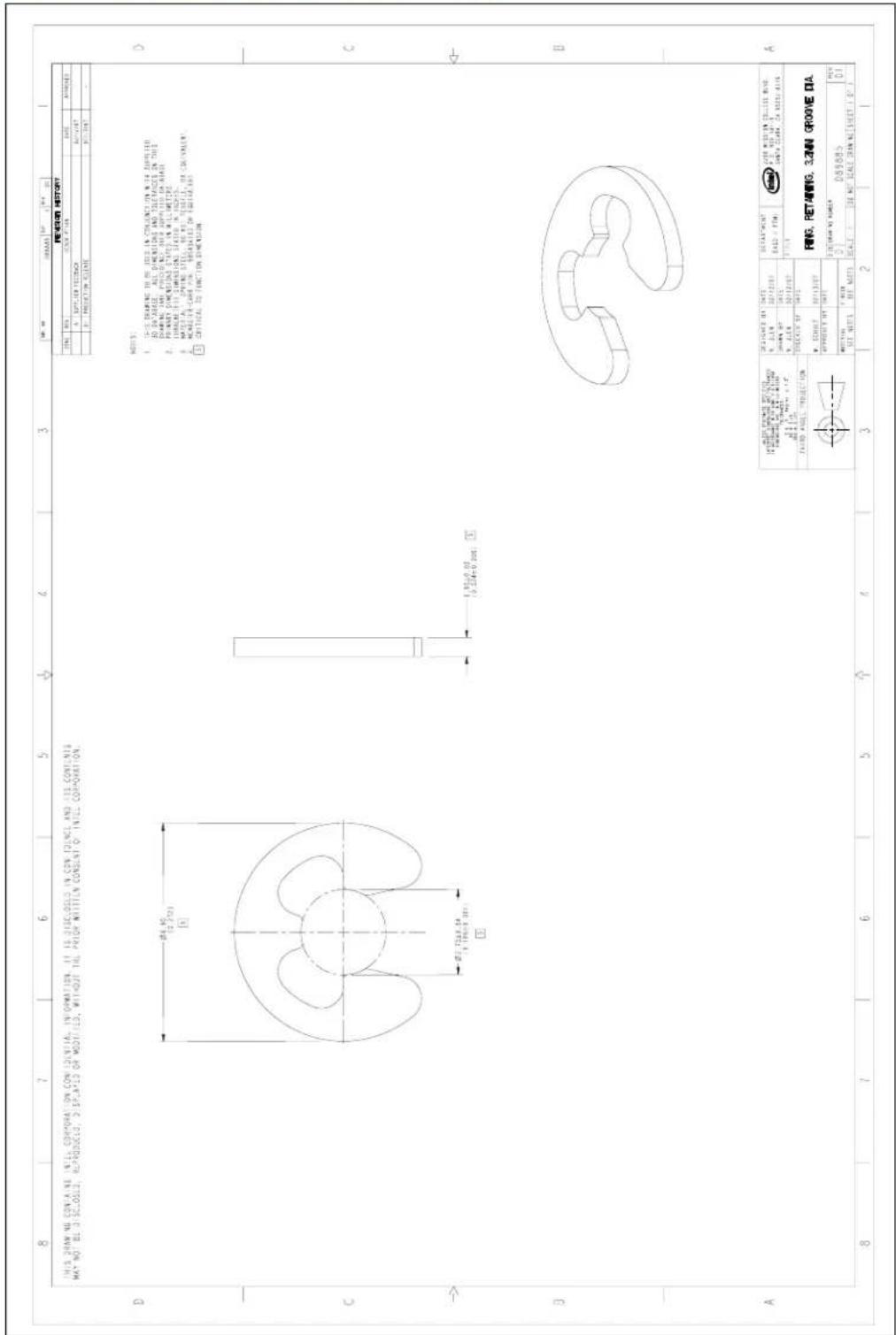
Figure B-12. Heatsink Load Cup (1U, 2U and Tower)

Figure B-13. 2U Collaborative Heatsink Assembly (Sheet 1 of 2)

Figure B-14. 2U Collaborative Heatsink Assembly (Sheet 2 of 2)
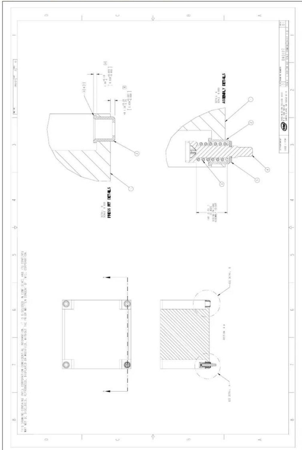
Figure B-15. 2U Collaborative Heatsink Volumetric (Sheet 1 of 2)
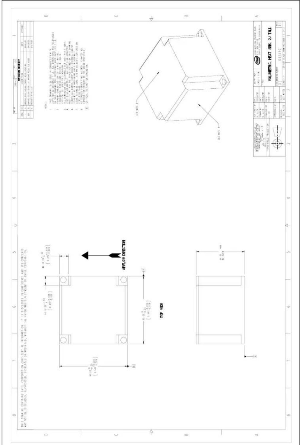
Figure B-16. 2U Collaborative Heatsink Volumetric (Sheet 2 of 2)
![THIS DRAWING CONTAINS INTEL CORPORATION CONFIDENTIAL INFORMATION IT IS DISCLOSED IN CONFIDENCE AND ITS CONTENTS MAY NOT BE DISCLOSED, REPRODUCED, DISPLAYS OR MODIFIED, WITHOUT THE PRIOR WRITTEN CONSENT OF INTEL CORPORATION D Ø3.06 3/2.06 [0.118 0.005] Ø2.11E 10.0017(A.B.D) C RIGHT ON RIGHT ON BOTTOM ON B RJ. 100 12.4100 (A) RJ. 0000.10 11.4110 (A+B) RIGHT ON RIGHT ON LEFTED ON OFF 100 RIGHT ON RIGHT ON RIGHT ON RIGHT ON RIGHT ON RIGHT ON RIGHT ON RIGHT ON RIGHT ON RIGHT ON RIGHT ON RIGHT ON RIGHT ON RIGHT ON RIGHT ON RIGHT ON RIGHT ON RIGHT ON RIGHT ON RIGHT ON RIGHT ON RIGHT ON RIGHT ON RIGHT ON RIGHT ON RIGHT ON RIGHT ON RIGHT ON RIGHT ON RIGHT ON RIGHT ON RIGHT ON RIGHT ON RIGHT ON](/content/2026/05/987880/images/b5434bd9885c58f08624cffccbde33bcd220576af5c3c3f63335a7de554af271.jpg)
Figure B-17. Tower Collaborative Heatsink Assembly (Sheet 1 of 2)

Figure B-18. Tower Collaborative Heatsink Assembly (Sheet 2 of 2)

Figure B-19. Tower Collaborative Heatsink Volumetric (Sheet 1 of 2)

Figure B-20. Tower Collaborative Heatsink Volumetric (Sheet 2 of 2)
![THIS DRAWING CONTAINS INTEL CORPORATION CONFIDENTIAL INFORMATION. IT IS DISCLOSED IN CONFIDENCE AND ITS CONTENTS MAY NOT BE DISCLOSED, RPRODUCED, DISPLAYED OR MODIFICATIONS. N HOLD THE PRIOR WRITTEN CONSENT D-IN-TE CORPORATION. DETAIL 1 SCALE: 6.000 4.5mm 12 [0.7/19] [0.8] BASE THICKNESS B A RIGHT TOP RIGHT TOP RIGHT TOP RIGHT TOP RIGHT TOP RIGHT TOP RIGHT TOP RIGHT TOP RIGHT TOP RIGHT TOP RIGHT TOP RIGHT TOP RIGHT TOP RIGHT TOP RIGHT TOP RIGHT TOP RIGHT TOP RIGHT TOP RIGHT TOP RIGHT TOP RIGHT TOP RIGHT TOP RIGHT TOP RIGHT TOP RIGHT TOP RIGHT Bottom VIEW](/content/2026/05/987880/images/78064897515510c772af443019f3f9657928b3a839d3f18f77e26dfe442ce255.jpg)
Figure B-21. 1U Reference Heatsink Assembly with TIM (Sheet 1 of 2)

Figure B-22. 1U Reference Heatsink Assembly with TIM (Sheet 2 of 2)
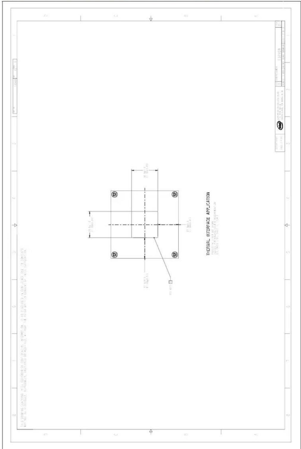
Figure B-23. 2U Reference Heatsink Assembly with TIM (Sheet 1 of 2)

Figure B-24. 2U Reference Heatsink Assembly with TIM (Sheet 2 of 2)

Figure B-25. Tower Reference Heatsink Assembly with TIM (Sheet 1 of 2)

Figure B-26. Tower Reference Heatsink Assembly with TIM (Sheet 2 of 2)

C Socket Mechanical Drawings
Table C-1 lists the mechanical drawings included in this appendix.
Table C-1. Mechanical Drawing List
| Drawing Description Figure Number | |
| "Socket Mechanical Drawing (Sheet 1 of 4)" Figure C-1 | |
| "Socket Mechanical Drawing (Sheet 2 of 4)" Figure C-2 | |
| "Socket Mechanical Drawing (Sheet 3 of 4)" Figure C-3 | |
| "Socket Mechanical Drawing (Sheet 4 of 4)" Figure C-4 |
Figure C-1. Socket Mechanical Drawing (Sheet 1 of 4)

Figure C-2. Socket Mechanical Drawing (Sheet 2 of 4)

Figure C-3. Socket Mechanical Drawing (Sheet 3 of 4)

Figure C-4. Socket Mechanical Drawing (Sheet 4 of 4)
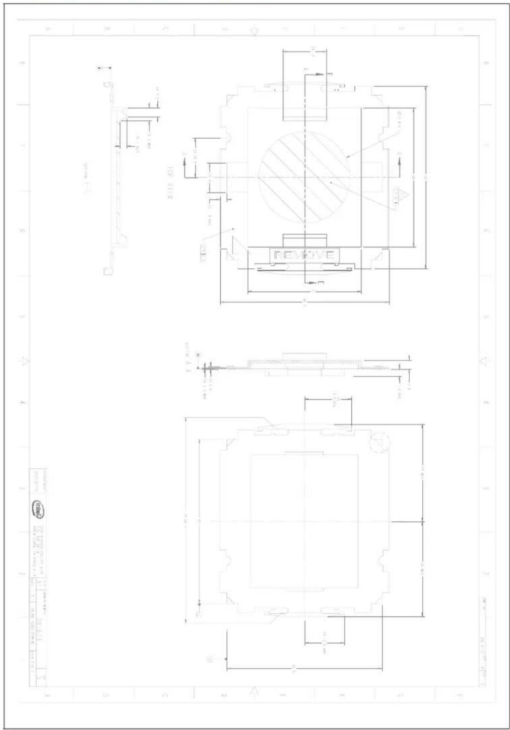
D Heatsink Load Metrology
To ensure compliance to max socket loading value listed in Table 4-3, and to meet the performance targets for Thermal Interface Material in Section 5.3, the Heatsink Static Compressive Load can be assessed using the items listed below:
- HP34970A DAQ
• Omegadyne load cell, 100 lbf max (LCKD-100) - Test board (0.062") with ILM & back plate installed
• 8 in-lbf pneumatic driver - Heatsink
• Gainestown Load Cell Fixture (Figure D-1)
Figure D-1. Intel® Xeon® Processor 5500 Series Load Cell Fixture

E Embedded Thermal Solutions
This section describes the LV processors and Embedded reference heatsinks for NEBS (Network Equipment Building Systems) compliant ATCA (Advanced Telecommunications Computing Architecture) systems. These LV processors are good for any form factor that needs to meet NEBS requirements.
E.1 Performance Targets
Table E-1 provides boundary conditions and performance targets for 1U and ATCA heatsinks. These values are used to generate processor thermal specifications and to provide guidance for heatsink design.
Table E-1. Boundary Conditions and Performance Targets
| Parameter Value Value | ||
| Altitude, system ambient temp Nominal/ Short-term | Sea level, 40°C/55C Sea level, 40 | °C/55C |
| TDP 60 W 38 W | ||
| T_LA^1,4 | 51.9/66.9°C | 50/65°C |
| _CA^2 | 0.302°C/W | 0.532°C/W |
| System height (form factor) ^3 | 1U (EEB) or ATCA | ATCA |
| Heatsink volumetric | 1U (90 x 90 x 27) or Custom ATCA (90 x 90 x 13mm + heat exchanger) | ATCA (90 x 90 x 13 mm) |
| Heatsink technology ^5 | Cu base, Cu fins | |
Notes:
- Local ambient temperature of the air entering the heatsink.
- Max target (mean + 3 sigma + offset) for thermal characterization parameter (Section 5.5.1).
- Reference system configuration. In a single wide ATCA blade the 60 W processor should be used in single socket only and the 38 W processor can be used in dual socket.
- Local Ambient Temperature written 50/65 °C means 50°C under Nominal conditions but 65°C is allowed for Short-Term NEBS excursions.
- Passive heatsinks with TIM.
- See Section 5.1 for standard 1U solutions that do not need to meet NEBS.
Detailed drawings for the ATCA reference heatsink can be found in Section E.3. Table E-1 above specifies _CA and pressure drop targets and Figure E-1 below shows _CA and pressure drop for the ATCA heatsink versus the airflow provided. Best-fit equations are provided to prevent errors associated with reading the graph.
Figure E-1. ATCA Heatsink Performance Curves

line
| CFM Through Fins | Ψca, C/W | ΔP, inch water | | ---------------- | -------- | -------------- | | 0 | 2.0 | 0.0 | | 5 | 1.5 | 0.1 | | 10 | 1.0 | 0.2 | | 15 | 0.8 | 0.3 | | 20 | 0.6 | 0.4 | | 25 | 0.5 | 0.5 | | 30 | 0.45 | 0.6 | | 35 | 0.4 | 0.7 | | Mean | 0.337 | - | | ΔP (×1e-04) | 1.3e-04 | +1.1e-02 | | ΔP (×1e-02) | 1.625 | - |Other LGA1366 compatible thermal solutions may work with the same retention.
E.2 Thermal Design Guidelines
E.2.1 NEBS Thermal Profile
Processors that offer a NEBS compliant thermal profile are specified in the Intel® Xeon® Processor 5500 Series Datasheet, Volume 1.
NEBS thermal profiles help relieve thermal constraints for Short-Term NEBS conditions. To help reliability, processors must meet the nominal thermal profile under standard operating conditions and can only rise up to the Short-Term spec for NEBS excursions (see Figure E-2). The definition of Short-Term time is clearly defined for NEBS Level 3 conditions but the key is that it cannot be longer than 360 hours per year.
Figure E-2. NEBS Thermal Profile
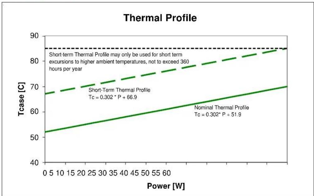
line
| Power [W] | Tcase [C] (Nominal Thermal Profile) | Tcase [C] (Short-Term Thermal Profile) | | --------- | ----------------------------------- | -------------------------------------- | | 0 | 52 | 67 | | 5 | 54 | 68 | | 10 | 56 | 69 | | 15 | 58 | 70 | | 20 | 60 | 71 | | 25 | 62 | 72 | | 30 | 64 | 73 | | 35 | 66 | 74 | | 40 | 68 | 75 | | 45 | 70 | 76 | | 50 | 72 | 77 | | 55 | 74 | 78 | | 60 | 76 | 79 | | 65 | 78 | 80 | | 70 | 80 | 81 | | 75 | 82 | 82 | | 80 | 84 | 83 | | 85 | 86 | 84 | | 90 | 88 | 85 | | 95 | 90 | 86 | | 100 | 92 | 87 |Notes:
1.) The thermal specifications shown in this graph are for reference only. See the Intel® Xeon® Processor 5500 Series Datasheet, Volume 1 for the Thermal Profile specifications. In case of conflict, the data in the datasheet supersedes any data in this figure.
2.) The Nominal Thermal Profile must be used for all normal operating conditions, or for products that do not require NEBS Level 3 compliance.
3.) The Short-Term Thermal Profile may only be used for short-term excursions to higher ambient operating temperatures, not to exceed 360 hours per year as compliant with NEBS Level 3.
4.) Implementation of either thermal profile should result in virtually no TCC activation.
5.) Utilization of a thermal solution that exceeds the Short-Term Thermal Profile, or which operates at the Short-Term Thermal Profile for a duration longer than the limits specified in Note 3 above, do not meet the processor thermal specifications and may result in permanent damage to the processor.
E.2.2 Custom Heat Sinks For UP ATCA
The Embedded specific 60W SKU is targeted for NEBS compliant 1U+ systems and UP ATCA configurations with custom thermal solutions. In order to cool this part in a single wide ATCA slot, a custom thermal solution will be required. Since solutions like this will be very configuration specific, this heat sink was not fully designed with retention and keep-out definitions.
In order to cool the additional power of a 60W processor in ATCA, the heat sink volume was increased. The assumption was that the heat sink could not grow wider because of VR and Memory placement, so a Remote Heat Exchanger (RHE) was used. The RHE is attached to the main heat sink with a heat pipe. The RHE gives additional convective surface area and gives the thermal solution access to more air. Samples of the following design were ordered and tested for thermal performance only.
Flotherm analysis shows that the following design can cool an LGA1366 TTV in an ATCA blade at 30CFM. The heat sink ca would be 0.50C / W at 55C ambient which falls below the thermal profile for the 60W processor.
Figure E-3. UP ATCA Thermal Solution

natural_image
Two copper heat sinks with ribbed heat sinks and a coiled cable, displayed on a plain surface (no text or symbols visible)Notes: Thermal sample only, retention not production ready.
Figure E-4. UP ATCA System Layout
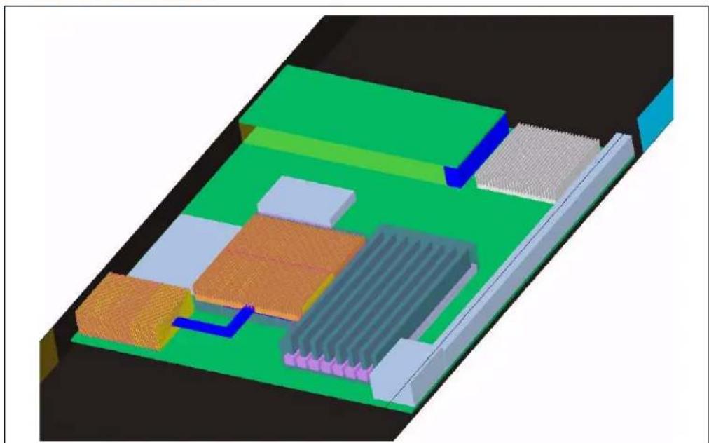
natural_image
3D schematic of a microfluidic chip or MEMS device with colored components and no visible text or symbolsNotes: Heat sink should be optimized for the layout.
Figure E-5. UP ATCA Heat Sink Drawing
![THIS DRAWING CONTAINS INTEL CORPORATION CONFIDENTIAL INFORMATION. IT IS DISCLOSED IN CONFIDENCE AND ITS CONTENTS MAY NOT BE DISCLOSED, REPRODUCED, DISPLATED OR MODIFIED, WITHOUT THE PRIDE WRITTEN CONSENT OF INTEL CORPORATION. B 145 [5.71] 50 [1.97] 10 [.39] 56.3 [2.61] 88.7 [3.49] A FINS: COUNT: 50 THICKNESS: 0.3 [.012] GAP: 1.50 [.060] FINS: COUNT: 36 THICKNESS: 0.3 [.0121] GAP: 2.5 [.10] 20 [.79] 3.5 [1.14] 13.43 [.53] A NOTES: 11 PRIMARY DIMENSIONS ARE IN MILLIMETERS, BRACKETED DIMENSIONS ARE IN INCHES, MM [INCH] 21 Ø6.0MM HEAT PIPE DEPARTMENT 2200 MISSION COLLEGE BLVD. P.O BOX 58119 SANTA CLARA CA 95052-8119 SIZE B CAGE CODE X DRAWING NUMBER NHM_UP_HS REV SCALE: 8.75 DO NOT SCALE DRAWING SHEET 1 OF 1](/content/2026/05/987880/images/0f8daf62098c339d7d4b8fe2d1dd5538a197027b0baa0408f2ed45e61668e1f7.jpg)
E.3 Mechanical Drawings and Supplier Information
See Appendix B for retention and keep out drawings.
The part number below represent Intel reference designs for a DP ATCA heatsink. Customer implementation of these components may be unique and require validation by the customer. Customers can obtain these components directly from the supplier below.
Table E-2. Embedded Heatsink Component Suppliers
| Assembly Component Description Supplier PN Supplier Contact Info | ||||
| Assembly, Heat Sink, Nehalem-EP, ATCA | ATCA Reference heatsinkIntel P/N E65918-001 | ATCA Copper Fin, Copper Base | Fujikura HSA-7901 | Fujikura AmericaAsh Ooe a_ooe@fujikura.com 408-748-6991Fujikura Taiwan BranchYao-Hsien Huang yeohsien@fujikuratw.com.tw 886(2)8788-4959 |
Table E-3. Mechanical Drawings List
| Parameter Value | |
| ATCA Reference Heat Sink Assembly (Sheet 1 of 2) Figure E-6 | |
| ATCA Reference Heat Sink Assembly (Sheet 2 of 2) Figure E-7 | |
| ATCA Reference Heatsink Fin and Base (Sheet 1 of 2) Figure E-8 | |
| ATCA Reference Heatsink Fin and Base (Sheet 2 of 2) Figure E-9 |
Figure E-6. ATCA Reference Heat Sink Assembly (Sheet 1 of 2)

Figure E-7. ATCA Reference Heat Sink Assembly (Sheet 2 of 2)
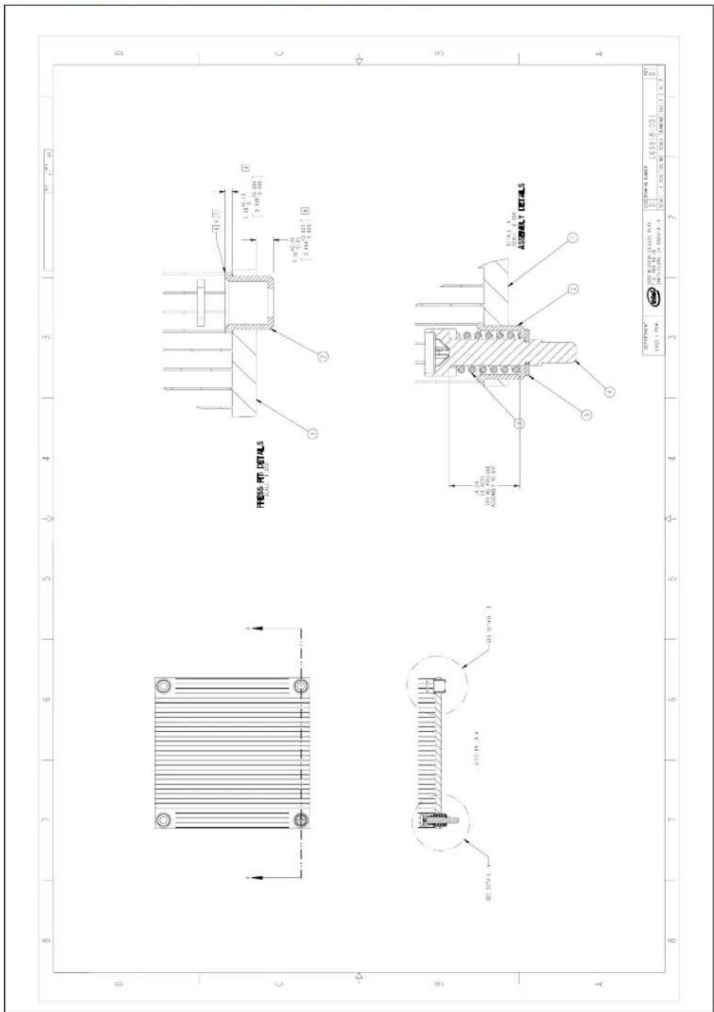
Figure E-8. ATCA Reference Heatsink Fin and Base (Sheet 1 of 2)
![THIS DRAWING CONTAINS INTEL CORPORATION CONTINENTIAL INFORMATION. IT IS DISCLOSED IN CONDUCT AND ITS CONTENTS WAY NOT BE DISCLOSED, RETRODUCED, DISPLAYED OR MODIFIED, WITHOUT THE PRIOR WRITTEN CONSENT OF INTEL CORPORATION TOP VIEW A 8 1 6 5 4 3 2 1 8 1 6 5 4 3 2 1 8 1 6 5 4 3 2 1 8 1 6 5 4 3 2 1 8 1 6 5 4 3 2 1 8 1 6 5 4 3 2 1 8 1 6 5 4 3 2 1 8 2 8 2 8 2 8 2 8 2 8 2 8 2 8 2 8 2 8 2 8 2 8 2 8 2 8 2 8 2 8 2 8 2 8 2 8 2 8 2 8 2 8 2 8 2 8 2 8 2 8 3 8 3 8 3 8 3 8 3 8 3 8 3 8 3 8 3 8 3 8 3 8 3 8 3 8 3 8 3 8 3 8 3 8 3 8 3 8 3 8 3 8 3 8.10 ±0.75 [0.60±0.00] [0.60±0.00] [0.60±0.00] [0.60±0.00] [0.60±0.00] [0.60±0.00] [0.60±0.00] [0.60±0.00] [0.60±0.00] [0.60±0.00] (1) (1) (1) (1) (1) (1) (1) (1) (1) (1) (1) (1) (1) (1) (1) (1) (1) (1) (1) (1) (1) (1) (1) (1) (1) (1) (1) (1) (1) (1) (1) (1) (1) (1) [1] [1] [1] [1] [1] [1] [1] [1] [1] [1] [1] [1] [1] [1] [1] [1] [1] [1] [1] [1] [1] [1] [1] [1] [1] [1] [1] [1] [1] [1] [1] [1] [1] [1] A TITLE NOTE: A NOTE: THIS DRAWING TO RE-USES IN CONJUNCTION WITH: DETAIL TO DO EXTRACTILE EQUITY OF THIS DRAWING TO PRESENTATION OF SURFURANCE. FOR THIS DRAWING THAT PRESENTATION OF SURFURANCE IS NOT TO BE USED. PROVEY DIMENSIONS STATE IN WILL NOT BEANS. PROCUTTAL DIMENSIONS STATED IN NOISES. DO FILLI TO CONNECTED SWITCH. CL D WINDTH AND SUPPLEMENT PER MIND. PTA. S-1/99A. BASE DIFFER, S-2/45 NEW #N. TIME SET TIP: Z=45 MIN, ALUMINUM, OS/7/99 MIN #N. WHIP NO, RUNZ, RUNP FIND, SURFACE, ADVENT. DO NOT TO CONNECT THE MACHINE TO ARE FOR ASSETS. LOCAL TAINTS ON: RTS MIN TO CUT? CAN TEST IN HEAT CABB END. MCHANGES, SWITCHING OR CONNECTION IN ALLOWED EN TOP SURE AND TO EXTRACT TO UNBEET FOR ASPECTRATIONS, STABILITY. DETAIL TO REJECT SHEET END TO MEAN/WIRE. CRITICAL TO FUNCTION DIMENSIONS. SIZE NOTE: A HEAT SHIK, CU BASE, CU FINS ITEMS: ITEMS BY: ITEMS NAME: DESCRIPTION: ITEMS NAME: ITEMS NAME: ITEMS NAME: ITEMS NAME: ITEMS NAME: ITEMS NAME: ITEMS NAME: ITEMS NAME: ITEMS NAME: ITEMS NAME: ITEMS NAME: ITEMS NAME: ITEMS NAME: ITEMS NAME: ITEMS NAME: ITEMS NAME: ITEMS NAME: ITEMS NAME: ITEMS NAME: ITEMS NAME: ITEMS Name: ITEMS NAME: ITEMS NAME: ITEMS NAME: ITEMS NAME: ITEMS NAME: ITEMS NAME: ITEMS NAME: ITEMS NAME: ITEMS NAME: ITEMS NAME: ITEMS NAME: ITEMS NAME: ITEMS NAME: ITEMS NAME: ITEMS NAME: ITEMS NAME: ITEMS NAME: ITEMS NAME: ITEMS NAME: ITEMS NICK, CU BASE, CU FINS TITLE DESCRIPTION: TITLE DESCRIPTION: TITLE DESCRIPTION: TITLE DESCRIPTION: TITLE DESCRIPTION: TITLE DESCRIPTION: TITLE DESCRIPTION: TITLE DESCRIPTION: TITLE DESCRIPTION: TITLE DESCRIPTION: TITLE DESCRIPTION: TITLE DESCRIPTION: TITLE DESCRIPTION: TITLE DESCRIPTION: TITLE DESCRIPTION: TITLE DESCRIPTION: TITLE DESCRIPTION: TITLE DESCRIPTION: TITLE DESCRIPTION: TITLE DESCRIPTION: TITLE DESCRIPTION: TITLE DESCRIPTION: TITLE DESCRIPTION: TITLE DESCRIPTION: TITLE DESCRIPTION: TITLE DESCRIPTION: TITLE DESCRIPTION: TITLE DESCRIPTION: TITLE DESCRIPTION: TITLE DESCRIPTION: TITLE DESCRIPTION: TITLE DESCRIPTION: TITLE DESCRIPTION: TITLE DESCRIPTION: TYPE NUMBER: TYPE NUMBER: TYPE NUMBER: TYPE NUMBER: TYPE NUMBER: TYPE NUMBER: TYPE NUMBER: TYPE NUMBER: TYPE NUMBER: TYPE NUMBER: TYPE NUMBER: TYPE NUMBER: TYPE NUMBER: TYPE NUMBER: TYPE NUMBER: TYPE NUMBER: TYPE NUMBER: TYPE NUMBER: TYPE NUMBER: TYPE NUMBER: TYPE NUMBER: TYPE NUMBER: TYPE NUMBER: TYPE NUMBER: TYPE NUMBER: TYPE NUMBER: TYPE NUMBER: TYPE NUMBER: TYPE NUMBER: TYPE NUMBER: TYPE NUMBER: TYPE NUMBER: TYPE NUMBER: TYPE NUMBER: TELE TYPE NUMBER: TELE TYPE NUMBER: TELE TYPE NUMBER: TELE TYPE NUMBER: TELE TYPE NUMBER: TELE TYPE NUMBER: TELE TYPE NUMBER: TELE TYPE NUMBER: TELE TYPE NUMBER: TELE TYPE NUMBER: TELE TYPE NUMBER: TELE TYPE NUMBER: TELE TYPE NUMBER: TELE TYPE NUMBER: TELE TYPE NUMBER: TELE TYPE NUMBER: TELE TYPE NUMBER: TELE TYPE NUMBER: TELE TYPE NUMBER: TELE TYPE NUMBER: TELE TYPICAL SIZE OF THIS DRAWING DESCRIPTION: DESCRIPTION BY : THIS DRAWING BY : THIS DRAWING BY : THIS DRAWING BY : THIS DRAWING BY : THIS DRAWING BY : THIS DRAWING BY : THIS DRAWING BY : THIS DRAWING BY : THIS DRAWING BY : THIS DRAWING BY : THIS DRAWING BY : THIS DRAWING BY : THIS DRAWING BY : THIS DRAWING BY : THIS DRAWING BY : THIS DRAWING BY : THIS DRAWING BY : THIS DRAWING BY : THIS DRAWING BY : THIS DRAWING BY : THIS DRAWINGS BY : THIS DRAWINGS BY : THIS DRAWINGS BY : THIS DRAWINGS BY : THIS DRAWINGS BY : THIS DRAWINGS BY : THIS DRAWINGS BY : THIS DRAWINGS BY : THIS DRAWINGS BY : THIS DRAWINGS BY : THIS DRAWINGS BY : THIS DRAWINGS BY : THIS DRAWINGS BY : THIS DRAWINGS BY : THIS DRAWINGS BY : THIS DRAWINGS BY : THIS DRAWINGS BY : THIS DRAWINGS BY : THIS DRAWINGS BY : THIS DRAWINGS BY : THIS DRAWGS BY : THIS DRAWGS BY : THIS DRAWGS BY : THIS DRAWGS BY : THIS DRAWGS BY : THIS DRAWGS BY : THIS DRAWGS BY : THIS DRAWGS BY : THIS DRAWGS BY : THIS DRAWGS BY : THIS DRAWGS BY : THIS DRAWGS BY : THIS DRAWGS BY : THIS DRAWGS BY : THIS DRAWGS BY : THIS DRAWGS BY : THIS DRAWGS BY : THIS DRAWGS BY : THIS DRAWGS BY : THIS DRAWGS BY : THIS DRAWGTY BY : THIS DRAWGS BY : THIS DRAWGS BY : THIS DRAWGS BY : THIS DRAWGS BY : THIS DRAWGS BY : THIS DRAWGS BY : THIS DRAWGS BY : THIS DRAWGS BY : THIS DRAWGS BY : THIS DRAWGS BY : THIS DRAWGS BY : THIS DRAWGS BY : THIS DRAWGS BY : THIS DRAWGS BY : THIS DRAWGS BY : THIS DRAWGS BY : THIS DRAWGS BY : THIS DRAWGS BY : THIS DRAWGS BY : THIS DRAWGGTY BY : THIS DRAWGS BY : THIS DRAWGS BY : THIS DRAWGS BY : THIS DRAWGS BY : THIS DRAWGS BY : THIS DRAWGS BY : THIS DRAWGS BY : THIS DRAWGS BY : THIS DRAWGS BY : THIS DRAWGS BY : THIS DRAWGS BY : THIS DRAWGS BY : THIS DRAWGS BY : THIS DRAWGS BY : THIS DRAWGS BY : THIS DRAWGS BY : THIS DRAWGS BY : THIS DRAWGS BY : THIS DRAWGS BY : THIS CAULIF CHEESE CHEESE CHEESE CHEESE CHEESE CHEESE CHEESE CHEESE CHEESE CHEESE CHEESE CHEESE CHEESE CHEESE CHEESE CHEESE CHEESE CHEESE CHEESE CHEESE CHEESE CHEESE CHEESE CHEESE CHEESE CHEESE CHEESE CHEESE CHEESE CHEESE CHEESE CHEESE CHEESE CHEESE CHINESE CHEESE CHEESE CHEESE CHEESE CHEESE CHEESE CHEESE CHEESE CHEESE CHEESE CHEESE CHEESE CHEESE CHEESE CHEESE CHEESE CHEESE CHEESE CHEESE CHEESE CHEESE CHEESE CHEESE CHEESE CHEESE CHEESE CHEESE CHEESE CHEESE CHEESE CHEESE CHEESE CHEECECHEMICAL SHEET COALDED FOR ITEMS OF THE INTERIOR OF THE INTERIOR OF THE INTERIOR OF THE INTERIOR OF THE INTERIOR OF THE INTERIOR OF THE INTERIOR OF THE INTERIOR OF THE INTERIOR OF THE INTERIOR OF THE INTERIOR OF THE INTERIOR OF THE INTERIOR OF THE INTERIOR OF THE INTERIOR OF THE INTERIOR OF THE INTERIOR OF THE INTERIOR OF THE INTERIOR OF THE INTERIOR OF THE INTERIOR OF THE INTERIOR OF THE INTERIOR OF THE INTERIOR OF THE INTERIOR OF THE INTERICUM OF THE INTERICUM OF THE INTERICUM OF THE INTERICUM OF THE INTERICUM OF THE INTERICUM OF THE INTERICUM OF THE INTERICUM OF THE INTERICUM OF THE INTERICUM OF THE INTERICUM OF THE INTERICUM OF THE INTERICUM OF THE INTERICUM OF THE INTERICUM OF THE INTERICUM OF THE INTERICUM OF THE INTERICUM OF THE INTERICUM OF THE INTERICUM OF THE INTERICUUM OF THE INTERICUM OF THE INTERICUM OF THE INTERICUM OF THE INTERICUM OF THE INTERICUM OF THE INTERICUM OF THE INTERICUM OF THE INTERICUM OF THE INTERICUM OF THE INTERICUM OF THE INTERICUM OF THE INTERICUM OF THE INTERICUM OF THE INTERICUM OF THE INTERICUM OF THE INTERICUM OF THE INTERICUM OF THE INTERICUM OF THE INTERICUM OF THE INTERIUM OF THE INTERICUM OF THE INTERICUM OF THE INTERICUM OF THE INTERICUM OF THE INTERICUM OF THE INTERICUM OF THE INTERICUM OF THE INTERICUM OF THE INTERICUM OF THE INTERICUM OF THE INTERICUM OF THE INTERICUM OF THE INTERICUM OF THE INTERICUM OF THE INTERICUM OF THE INTERICUM OF THE INTERICUM OF THE INTERICUM OF THE INTERICUM OF THE INTERCUM OF THE INTERICUM OF THE INTERICUM OF THE INTERICUM OF THE INTERICUM OF THE INTERICUM OF THE INTERICUM OF THE INTERICUM OF THE INTERICUM OF THE INTERICUM OF THE INTERICUM OF THE INTERICUM OF THE INTERICUM OF THE INTERICUM OF THE INTERICUM OF THE INTERICUM OF THE INTERICUM OF THE INTERICUM OF THE INTERICUM OF THE INTERICUM OF THE INTERICCUM OF THE INTERICUM OF THE INTERICUM OF THE INTERICUM OF THE INTERICUM OF THE INTERICUM OF THE INTERICUM OF THE INTERICUM OF THE INTERICUM OF THE INTERICUM OF THE INTERICUM OF THE INTERICUM OF THE INTERICUM OF THE INTERICUM OF THE INTERICUM OF THE INTERICUM OF THE INTERICUM OF THE INTERICUM OF THE INTERICUM OF THE INTERICUM OF THE INTERICH UNT. THE ITEMS CONTAINED FROM CURRENT ITEMS DESCRIPTION: DESCRIPTION BY: THIS DRAWING BY: THIS DRAWING BY: THIS DRAWING BY: THIS DRAWING BY: THIS DRAWING BY: THIS DRAWING BY: THIS DRAWING BY: THIS DRAWING BY: THIS DRAWING BY: THIS DRAWING BY: THIS DRAWING BY: THIS DRAWING BY: This TYPICAL SIZE AND TYPE Characteristics TITLE DESCRIPTION: TITLE DESCRIPTION: TITLE DESCRIPTION: TITLE DESCRIPTION: TITLE DESCRIPTION: TITLE DESCRIPTION: TITLE DESCRIPTION: TITLE DESCRIPTION: TITLE DESCRIPTION: TITLE DESCRIPTION: TITLE DESCRIPTION: TITLE DESCRIPTION: TITLE DESCRIPTION: TITLE DESCRIPTION: TITLE DESCRIPTION: TITLE DESCRIPTION: TITLE DESCRIPTION: TITLE DESCRIPTION: TITLE DESCRIPTION: TITLE DESCRIPTION: TITLE DESCRIPTION: TITLE DESCRIPTION: TITLE DESCRIPTION: TITLE DESCRIPTION: TITLE DESCRIPTION: TITLE DESCRIPTION: TITLE DESCRIPTION: TITLE DESCRIPTION: TITLE DESCRIPTION: TITLE DESCRIPTION: TITLE DESCRIPTION: TITLE DESCRIPTION: TITLE DESCRIPTION): TITLE DESCRIPTION: TITLE DESCRIPTION: TITLE DESCRIPTION: TITLE DESCRIPTION: TITLE DESCRIPTION: TITLE DESCRIPTION: TITLE DESCRIPTION: TITLE DESCRIPTION: TITLE DESCRIPTION: TITLE DESCRIPTION: TITLE DESCRIPTION: TITLE DESCRIPTION: TITLE DESCRIPTION: TITLE DESCRIPTION: TITLE DESCRIPTION: TITLE DESCRIPTION: TITLE DESCRIPTION: TITLE DESCRIPTION: TITLE DESCRIPTION: TITLE DESCRIPTION: TITLE DESCRIPTION: TITLE DESCRIPTION: TITLE DESCRIPTION: TITLE DESCRIPTION: TITLE DESCRIPTION: TITLE DESCRIPTION: TITLE DESCRIPTION: TITLE DESCRIPTION: TITLE DESCRIPTION: TITLE DESCRIPTION: TITLE DESCRIPTION: TITLE DESCRIPTION: TITLE DESCRIPTION: ITL TYPICAL SIZE AND TYPE Characteristics ITL TYPICAL SIZE AND TYPE Characteristics ITL TYPICAL SIZE AND TYPE Characteristics ITL TYPICAL SIZE AND TYPE Characteristics ITL TYPICAL SIZE AND TYPE Characteristics ITL TYPICAL SIZE AND TYPE Characteristics ITL TYPICAL SIZE AND TYPE Characteristics ITL TYPICAL SIZE AND TYPE Characteristics ITL TYPICAL SIZE AND TYPE Characteristics ITL TYPICAL SIZE AND TYPE Characteristics ITL TYPICAL SIZE AND TYPE Characteristics](/content/2026/05/987880/images/452d696d152f1809f7f2471c6aea93927b21c7d736cbad12e9abee35f721b4c8.jpg)
Figure E-9. ATCA Reference Heatsink Fin and Base (Sheet 2 of 2)

F Processor Installation Tool
The following optional tool is designed to provide mechanical assistance during processor installation and removal.
Contact the supplier for availability:
Billy Hsieh
billy.hsieh@tycoelectronics.com
+81 44 844 8292
Figure F-1. Processor Installation Tool

- Intel® Xeon® Processor 5500 Series
- Contents
- Introduction....9
- LGA1366 Socket 13
- Independent Loading Mechanism (ILM) 21
- LGA1366 Socket and ILM Electrical, Mechanical, and Environmental Specifications. 27
- Thermal Solutions 31
- intel®
- Quality and Reliability Requirements 43
- A Component Suppliers....47
- F Processor Installation Tool 97
- Figures
- Tables
- Revision History
- Introduction
- References
- Notes:
- Definition of Terms
- LGA1366 Socket
- Board Layout
- Attachment to Motherboard
- Socket Components
- Socket Body Housing
- Solder Balls
- Contacts
- Pick and Place Cover
- Package Installation / Removal
- Socket Standoffs and Package Seating Plane
- Durability
- Markings
- Component Insertion Forces
- Socket Size
- LGA1366 Socket NCTF Solder Joints
- Independent Loading Mechanism (ILM)
- Design Concept
- ILM Cover Assembly Design Overview
- ILM Back Plate Design Overview
- Assembly of ILM to a Motherboard
- LGA1366 Socket and ILM Electrical, Mechanical, and Environmental Specifications
- Component Mass
- Package/ Socket Stackup Height
- Socket Maximum Temperature
- Loading Specifications
- Electrical Requirements
- Environmental Requirements
- Thermal Solutions
- Performance Targets
- 25.5 mm Tall Heatsink
- Heat Pipe Considerations
- Assembly
- Thermal Interface Material (TIM)
- Structural Considerations
- Thermal Design
- Thermal Characterization Parameter
- Dual Thermal Profile
- Thermal Features
- Fan Speed Control
- T CONTROL Guidance
- PECI Averaging and Catastrophic Thermal Management
- Intel® Turbo Boost Technology
- Thermal Guidance
- Thermal Excursion Power for 95 W Processor
- Thermal Excursion Power for 80 W Processor
- Absolute Processor Temperature
- Quality and Reliability Requirements
- Test Conditions
- Intel Reference Component Validation
- Board Functional Test Sequence
- Post-Test Pass Criteria
- Recommended BIOS/ Processor/ Memory Test Procedures
- Material and Recycling Requirements
- A Component Suppliers
- A.1 Intel Enabled Supplier Information
- A.1.1 Intel Reference Thermal Solution
- A.1.2 Intel Collaboration Thermal Solution
- A.1.3 Alternative Thermal Solution
- A.1.4 Socket and ILM Components
- B Mechanical Drawings
- C Socket Mechanical Drawings
- D Heatsink Load Metrology
- E Embedded Thermal Solutions
- E.1 Performance Targets
- E.2 Thermal Design Guidelines
- E.2.1 NEBS Thermal Profile
- E.2.2 Custom Heat Sinks For UP ATCA
- E.3 Mechanical Drawings and Supplier Information
- F Processor Installation Tool
Brand : IBM
Model : 46M1079
Category : Processor