
HNS2600JFF - Motherboard INTEL - Free user manual and instructions
Find the device manual for free HNS2600JFF INTEL in PDF.


| Product Type | Server Motherboard |
| Model | Intel HNS2600JFF (S2600JFF SKU) |
| Form Factor | Half-width, 6.4" x 17.8" (153 mm x 453 mm) |
| Processor Support | One or two Intel Xeon E5-2600/E5-2600v2 series, LGA 2011, up to 135W TDP |
| Memory | 8 DIMM slots (4 per CPU), DDR3 RDIMM/LRDIMM/UDIMM with ECC, up to 1866 MT/s |
| Chipset | Intel C600-A Platform Controller Hub (PCH) |
| Expansion Slots | 3 PCIe Gen3 x16 riser slots (1 from CPU2, 2 from CPU1) |
| Network | Dual GbE via Intel I350 controller |
| InfiniBand | Single port FDR (14 Gbps) via Mellanox ConnectX-3 QSFP |
| Storage Interfaces | 1x SATA 6 Gb/s onboard, 4x SAS/SATA (3 Gb/s) via bridge board, optional storage upgrade key |
| RAID Support | Intel RSTe (0/1/5/10) or LSI SW RAID (0/1/5/10) for SATA; optional ESRT2 for SAS |
| Video | Integrated 2D video via BMC, 128 MB DDR2, DB15 connector |
| Management | Integrated BMC with IPMI 2.0, KVM, SOL, support for Intel RMM4 Lite |
| Power Connectors | Two 2x3 (6-pin) connectors for 12V and 5V standby |
| Fan Support | Three dual-rotor fan headers with PWM control |
| I/O Ports (Rear) | DB15 VGA, 2x RJ45, 2x USB 2.0, QSFP for InfiniBand, status LEDs |
| Internal Headers | 1x USB 2.0, serial port, RMM4 Lite, storage upgrade key, bridge board, IPMB |
| BIOS Features | UEFI, extensive configuration options, POST diagnostics LEDs, error logging |
| Environmental Limits | Operating: 10°C to 35°C (typical), altitude derating, fan profile control |
| Regulatory | Safety and emissions compliant per Intel specifications |
| Warranty | Refer to Intel terms and conditions; standard server board warranty |
Frequently Asked Questions - HNS2600JFF INTEL
User questions about HNS2600JFF INTEL
0 question about this device. Answer the ones you know or ask your own.
Ask a new question about this device
Download the instructions for your Motherboard in PDF format for free! Find your manual HNS2600JFF - INTEL and take your electronic device back in hand. On this page are published all the documents necessary for the use of your device. HNS2600JFF by INTEL.
USER MANUAL HNS2600JFF INTEL
Technical Product Specification
Intel order number G31608-014

Revision 2.3
February 2014
Revision History
| Date | Revision Number | Modifications |
| December, 2011 | 1.0 | Initial release. |
| February, 2012 | 1.1 | Added BMC sensor table and features. |
| May, 2012 | 1.2 | ▪ Updated Design Specifications and ASHRAE specification.▪ Added NTB support in BIOS.▪ Updated board block diagram. |
| July, 2012 | 1.3 | Updated InfiniBand* recommendation. |
| September, 2012 | 1.4 | ▪ Updated Node Manager IPMI Integrated Sensors.▪ Updated extended memory support. |
| February, 2013 | 1.5 | ▪ Updated board block diagram.▪ Updated E5-2600V2 processor support. |
| June, 2013 | 1.6 | Updated memory test scope. |
| August, 2013 | 1.7 | Updated Jumper Usage, BIOS menu changes, and Video POST Code Errors. |
| September, 2013 | 1.8 | Updated POST LED decode table, Video POST code table, and POST Error Beep codes. |
| October, 2013 | 1.9 | Updated decode table of system status LED. |
| November, 2013 | 2.0 | Updated LRDIMM support. |
| December, 2013 | 2.1 | Updated jumper usage description. |
| January, 2014 | 2.2 | Updated new BIOS menu based on E5-2600v2 processor. |
| February, 2014 | 2.3 | Updated processor PCIe root port mapping. |
Disclaimers
INFORMATION IN THIS DOCUMENT IS PROVIDED IN CONNECTION WITH INTEL PRODUCTS. NO LICENSE, EXPRESS OR IMPLIED, BY ESTOPPEL OR OTHERWISE, TO ANY INTELLECTUAL PROPERTY RIGHTS IS GRANTED BY THIS DOCUMENT. EXCEPT AS PROVIDED IN INTEL'S TERMS AND CONDITIONS OF SALE FOR SUCH PRODUCTS, INTEL ASSUMES NO LIABILITY WHATSOEVER AND INTEL DISCLAIMS ANY EXPRESS OR IMPLIED WARRANTY, RELATING TO SALE AND/OR USE OF INTEL PRODUCTS INCLUDING LIABILITY OR WARRANTIES RELATING TO FITNESS FOR A PARTICULAR PURPOSE, MERCHANTABILITY, OR INFRINGEMENT OF ANY PATENT, COPYRIGHT OR OTHER INTELLECTUAL PROPERTY RIGHT.
A "Mission Critical Application" is any application in which failure of the Intel Product could result, directly or indirectly, in personal injury or death. SHOULD YOU PURCHASE OR USE INTEL'S PRODUCTS FOR ANY SUCH MISSION CRITICAL APPLICATION, YOU SHALL INDEMNIFY AND HOLD INTEL AND ITS SUBSIDIARIES, SUBCONTRACTORS AND AFFILIATES, AND THE DIRECTORS, OFFICERS, AND EMPLOYEES OF EACH, HARMLESS AGAINST ALL CLAIMS COSTS, DAMAGES, AND EXPENSES AND REASONABLE ATTORNEYS' FEES ARISING OUT OF, DIRECTLY OR INDIRECTLY, ANY CLAIM OF PRODUCT LIABILITY, PERSONAL INJURY, OR DEATH ARISING IN ANY WAY OUT OF SUCH MISSION CRITICAL APPLICATION, WHETHER OR NOT INTEL OR ITS SUBCONTRACTOR WAS NEGLIGENT IN THE DESIGN, MANUFACTURE, OR WARNING OF THE INTEL PRODUCT OR ANY OF ITS PARTS.
Intel may make changes to specifications and product descriptions at any time, without notice. Designers must not rely on the absence or characteristics of any features or instructions marked "reserved" or "undefined". Intel reserves these for future definition and shall have no responsibility whatsoever for conflicts or incompatibilities arising from future changes to them. The information here is subject to change without notice. Do not finalize a design with this information.
The products described in this document may contain design defects or errors known as errata which may cause the product to deviate from published specifications. Current characterized errata are available on request.
Contact your local Intel sales office or your distributor to obtain the latest specifications and before placing your product order.
Copies of documents which have an order number and are referenced in this document, or other Intel literature, may be obtained by calling 1-800-548-4725, or go to: http://www.intel.com/design/literature.
Intel and Xeon are trademarks of Intel Corporation in the U.S. and/or other countries.
*Other names and brands may be claimed as the property of others.
Copyright © 2014 Intel Corporation. All rights reserved.
Table of Contents
1. Introduction .... 1
1.1 Section Outline....1
1.2 Server Board Use Disclaimer 2
2. Server Board Overview ....3
2.1 Server Board Connector and Component Layout....5
2.1.1 Board Rear Connector Placement....6
2.1.2 Server Board Mechanical Drawings 7
3. Product Architecture Overview ....8
3.1 High Level Product Features....8
3.2 Processor Support 10
3.2.1 Processor Socket Assembly....10
3.2.2 Processor Population Rules 11
3.3 Processor Function Overview....13
3.3.1 Intel ^® QuickPath Interconnect....14
3.3.2 Integrated Memory Controller (IMC) and Memory Subsystem....14
3.3.3 Processor Intergrated I/O Module (I/O)....20
3.4 Intel ^® C600-A/B PCH Functional Overview 24
3.4.1 PCI Express ^* 25
3.4.2 Non-Transparent Bridge....25
3.4.3 Universal Serial Bus (USB) 26
3.4.4 Serial Attached SCSI (SAS) and Serial ATA (SATA) Controller....26
3.4.5 PCI Interface 27
3.4.6 Low Pin Count (LPC) Interface 27
3.4.7 Digital Media Interface (DMI)......27
3.4.8 Serials Peripheral Interface (SPI) 27
3.4.9 Compatibility Modules (DMA Controller, Timer/Counters, Interrupt Controller) .....27
3.4.10 Advanced Programmable Interrupt Controller (APIC)....28
3.4.11 Real Time Clock (RTC) 28
3.4.12 GPIO....28
3.4.13 Enhanced Power Management 28
3.4.14 Fan Speed Control....28
3.4.15 Intel ^® Virtualization Technology for Direct I/O (Intel ^® VT-d)....29
3.4.16 KVM/Serial Over LAN (SOL) Function....29
3.4.17 IDE-R Function....29
3.4.18 Manageability....29
3.4.19 System Management Bus (SMBus 2.0*) 30
3.4.20 Network Interface Controller (NIC) 30
3.5 InfiniBand* Controller 32
3.5.1 Device Interfaces ....33
3.5.2 Quad Small Form-factor Pluggable (QSFP) Connector 33
3.6 Integrated Baseboard Management Controller Overview 34
3.6.1 Super I/O Controller 36
3.6.2 Graphics Controller and Video Support 36
3.6.3 Remote KVM....37
4. Platform Management Functional Overview....39
4.1 Baseboard Management Controller (BMC) Firmware Feature Support......39
4.1.1 IPMI 2.0 Features....39
4.1.2 Non-IPMI Features....40
4.1.3 New Manageability Features....41
4.2 Advanced Configuration and Power Interface (ACPI) 43
4.3 Platform Management SMBus* and I ^2 C Implementation....43
4.4 BMC Internal Timestamp Clock....44
4.5 Sensor Monitoring 44
4.6 Messaging Interfaces....44
4.6.1 Channel Management....45
4.6.2 User Model....45
4.6.3 Sessions 46
4.6.4 BMC LAN Channels 47
4.6.5 IPv6 Support 48
4.6.6 BMC IP Address Configuration....49
4.6.7 DHCP BMC Hostname....51
4.6.8 Address Resolution Protocol (ARP)....52
4.6.9 Virtual Local Area Network (VLAN) 52
4.6.10 Secure Shell (SSH) 53
4.6.11 Serial-over-LAN (SOL 2.0) 53
4.6.12 Platform Event Filter (PEF)....53
4.6.13 LAN Alerting....54
4.6.14 SNMP Platform Event Traps (PETs) 54
4.6.15 Alert Policy Table 54
4.6.16 Email Alerting....54
4.6.17 SM-CLP (SM-CLP Lite) 54
4.7 System Event Log (SEL) 55
4.7.1 Servicing Events 55
4.7.2 SEL Entry Deletion....55
4.7.3 SEL Erasure....55
4.7.4 SEL Extension Capabilities ....55
4.8 Sensor Data Record (SDR) Repository 56
4.9 Field Replaceable Unit (FRU) Inventory Device 56
4.10 Diagnostics and Beep Code Generation....56
4.11 Diagnostics Interrupt (NMI)....56
4.12 BMC Basic and Advanced Management Features 57
4.12.1 Enabling Advanced Manageability Features....58
4.12.2 Media Redirection....60
4.12.3 Embedded Web Server 61
4.12.4 Data Center Management Interface (DCMI) 62
4.12.5 Local Directory Authentication Protocol (LDAP) 63
4.12.6 Platform/Chassis Management 63
4.12.7 Thermal Control 63
4.12.8 Node Power On/Off Control....65
4.13 Intel ^® Intelligent Power Node Manager....65
4.13.1 Overview 65
4.13.2 Features....65
4.14 Management Engine (ME)....66
4.14.1 Overview....66
4.14.2 BMC – Management Engine (ME) Distributed Model 66
4.14.3 ME System Management Bus (SMBus*) Interface 67
4.14.4 BMC – Management Engine Interaction....67
4.14.5 ME Power and Firmware Startup....68
4.14.6 SmaRT/CLST 68
4.15 Other Platform Management....69
4.15.1 Wake On LAN (WOL)....69
4.15.2 PCI Express* Power Management 69
4.15.3 PMBus ^* 69
4.15.4 Node Power Policies....69
- BIOS Setup Interface....70
5.1 HotKeys Supported during POST....70
5.2 POST Logo/Diagnostic Screen....70
5.3 BIOS Boot Pop-up Menu....71
5.4 BIOS Setup Utility 71
5.4.1 BIOS Setup Operation....71
5.4.2 BIOS Setup Utility Screens....74
5.5 Loading BIOS Defaults....123
- Configuration Jumpers....124
6.1 Force Integrated BMC Update (J6B1) 125
6.2 Force ME Update (J1E2) 126
6.3 Password Clear (J1B6) 127
6.4 BIOS Recovery Mode (J1E1) 127
6.5 Reset BIOS Settings (J1D5)....128
- Connector/Header Locations and Pin-out ....130
7.1 Power Connectors....130
7.2 System Management Headers....130
7.2.1 Intel ^ Remote Management Module 4 (Intel ^ RMM4 Lite) Connector....130
7.2.2 IPMB Header....130
7.3 Bridge Board Connector....130
7.3.1 Power Button....132
7.3.2 Reset Button 132
7.3.3 Chassis Identify Button....132
7.3.4 Power LED....132
7.3.5 System Status LED 133
7.3.6 Chassis ID LED....135
7.4 I/O Connectors....135
7.4.1 PCI Express* Connectors....135
7.4.2 VGA Connector....142
7.4.3 NIC Connectors....142
7.4.4 SATA Connectors 143
7.4.5 Hard Drive Activity (Input) LED Header 143
7.4.6 Storage Upgrade Key Connector....144
7.4.7 Serial Port Connectors 144
7.4.8 USB Connectors 144
7.4.9 QSFP for InfiniBand* 145
7.5 Fan Headers 145
7.6 Chassis Intrusion....146
- Intel ^® Light-Guided Diagnostics ....147
8.1 Front Panel Support....147
8.1.1 System ID LED....147
8.1.2 System Status LED 147
8.1.3 Network Link/Activity LED 147
8.1.4 Dedicated InfiniBand* Link/Activity LED 148
8.2 POST Code Diagnostic LEDs....148
- Environmental Limits Specification ....150
9.1 System Level Environmental Considerations .... 150
9.1.1 Set Throttling Mode....151
9.1.2 Altitude....151
9.1.3 Set Fan Profile 151
9.1.4 Fan PWM Offset....151
9.1.5 Quiet Fan Idle Mode....151
9.1.6 Thermal Sensor Input for Fan Speed Control 152
9.2 Processor Thermal Design Power (TDP) Support 153
- Power Supply Specification Guidelines....154
10.1 Power Supply DC Output Connector....154
10.2 Power Supply DC Output Specification 154
10.2.1 Output Power/Currents....154
10.2.2 Standby Output....154
10.2.3 Voltage Regulation....155
10.2.4 Dynamic Loading 155
10.2.5 Capacitive Loading....155
10.2.6 Grounding....155
10.2.7 Closed Loop Stability....155
10.2.8 Residual Voltage Immunity in Standby Mode 156
10.2.9 Common Mode Noise....156
10.2.10 Soft Starting 156
10.2.11 Zero Load Stability Requirements 156
10.2.12 Hot Swap Requirements 156
10.2.13 Forced Load Sharing....156
10.2.14 Ripple/Noise....156
10.2.15 Timing Requirement....157
Appendix A: Integration and Usage Tips ....159
Appendix B: Integrated BMC Sensor Tables....160
Appendix C: BIOS Sensors and SEL Data 177
Appendix D: Node Manager 2.0 IPMI Integrated Sensors ....184
Appendix E: POST Code LED Decoder 185
Appendix F: Video POST Code Errors....190
Glossary 196
Reference Documents....199
List of Figures
Figure 1. Intel ^® Server Board S2600JF (InfiniBand* SKU)....3
Figure 2. Intel ^® Server Board S2600JF Components ....5
Figure 3. Rear Panel Connector Placement....6
Figure 4. Baseboard and Mounting Holes ....7
Figure 5. Intel ^® Server Board S2600JF Functional Block Diagram .....9
Figure 6. Processor Socket Assembly....10
Figure 7. Processor Socket ILM Variations .....11
Figure 8. Processor with IMC Functional Block Diagram....14
Figure 9. Intel ^® Server Board S2600JF Family DIMM Slot Layout....18
Figure 10. General Functional Block Diagram of Processor I/O Subsystem....20
Figure 11. PCI Express* Lane Distribution Scheme ......21
Figure 12. PCIe Riser for Slot 1 ......23
Figure 13. PCIe Riser for Slot 2 ....23
Figure 14. Intel ^® C600-A/B PCH Connection....24
Figure 15. 1GbE NIC Port LED ....31
Figure 16. ConnectX'-3 Function Block Diagram....32
Figure 17. Connection between ConnectX ^* -3 and QSFP....33
Figure 18. Integrated BMC Implementation Overview ......34
Figure 19. Integrated BMC Functional Block Diagram....35
Figure 20. Management Engine Distribution Model....67
Figure 21. Main Screen....76
Figure 22. Advanced Screen....78
Figure 23. Processor Configuration Screen....79
Figure 24. Power and Performance Configuration Screen ....83
Figure 25. Memory Configuration Screen....86
Figure 26. Memory RAS and Performance Configuration Screen ....88
Figure 27. Mass Storage Controller Configuration Screen ....89
Figure 28. PCI Configuration Screen....91
Figure 29. NIC Configuration Screen ....93
Figure 30. UEFI Network Stack Configuration Screen....96
Figure 31. UEFI Option ROM Configuration Screen....97
Figure 32. i350 NIC Configuration Screen....97
Figure 33. IIO PCI Express Lane Partitioning....99
Figure 34. Processor PCIe Link Speed Configuration Screen 99
Figure 35. Processor PCIe Link Speed Configuration in Detail....100
Figure 36. Serial Port Configuration Screen....100
Figure 37. USB Configuration Screen....101
Figure 38. System Acoustic and Performance Configuration Screen 103
Figure 39. Security Screen....105
Figure 40. Server Management Screen ....107
Figure 41. Console Redirection Screen....109
Figure 42. System Information Screen....111
Figure 43. BMC LAN Configuration Screen....112
Figure 44. Boot Options Screen....114
Figure 45. CDROM Order Screen....116
Figure 46. Hard Disk Order Screen....117
Figure 47. Floppy Order Screen....117
Figure 48. Network Device Order Screen....118
Figure 49. BEV Device Order Screen....119
Figure 50. Add EFI Boot Option Screen....119
Figure 51. Delete EFI Boot Option Screen....120
Figure 52. Boot Manager Screen ....121
Figure 53. Error Manager Screen....122
Figure 54. Save & Exit Screen....122
Figure 55. Jumper Blocks (J6B1, J1E2, J1E3, J1E1, and J1D5)....124
Figure 56. System Status LED (A) and ID LED (B) 133
Figure 57. Rear Panel Diagnostic LEDs (Block A)....149
Figure 58. Fan Control Model....153
Figure 59. Turn On/Off Timing (Power Supply Signals)....158
Figure 60. Diagnostic LED Placement Diagram (Block A)....185
List of Tables
Table 1. Intel ^® Server Board S2600JF Feature Set....3
Table 2. Intel ^® Server Board S2600JF Features....8
Table 3. Mixed Processor Configurations....12
Table 4. Color Definition....16
Table 5. UDIMM Support Guidelines....16
Table 6. RDIMM Support Guidelines....16
Table 7. LRDIMM Support Guidelines....17
Table 8. Intel ^® Server Board S2600JF DIMM Nomenclature ..... 18
Table 9. CPU1 and CPU2 PCIe Connectivity .....22
Table 10. Intel ^® Server Board S2600JF SATA/SAS Port....26
Table 11. Intel ^® RAID C600 Storage Upgrade Key Options for S2600JF .....27
Table 12. NIC Status LED....31
Table 13. Network Port Configuration ....33
Table 14. Supported Video Modes....37
Table 15. Dual Video Option....37
Table 16. ACPI Power States....43
Table 17. Standard Channel Assignments ...... 45
Table 18. Default User Values ......46
Table 19. Channel/Media-Specific Minimum Number of Sessions....46
Table 20. Factory Configured PEF Table Entries....53
Table 21. BMC Beep Codes....56
Table 22. NMI Signal Generation and Event Logging....57
Table 23. Basic and Advanced Management Features ....57
Table 24. Management Features and Benefits....58
Table 25. Fan Profile Mapping ....64
Table 26. POST HotKeys Recognized ....70
Table 27. BIOS Setup Page Layout ....72
Table 28. BIOS Setup: Keyboard Command Bar ....73
Table 29. Screen Map....75
Table 30. Setup Utility – Main Screen Fields....77
Table 31. Setup Utility – Advanced Screen Fields....78
Table 32. Setup Utility – Processor Configuration Screen Fields....80
Table 33. Setup Utility – Power and Performance Configuration Screen Fields....83
Table 34. Power/Performance Profiles....84
Table 35. Setup Utility – Memory Configuration Screen Fields....86
Table 36. Setup Utility – Memory RAS and Performance Configuration Screen Fields....88
Table 37. Setup Utility – Mass Storage Controller Configuration Screen Fields....89
Table 38. Setup Utility – PCI Configuration Screen Fields....91
Table 39. Setup Utility – NIC Configuration Screen Fields ......94
Table 40. Setup Utility – UEFI Network Stack Configuration Screen Fields....96
Table 41. Setup Utility – UEFI Option ROM Configuration Screen Fields....97
Table 42. i350 NIC Configuration Screen Fields....98
Table 43. Setup Utility – Processor PCIe Link Speed Configuration Screen Fields .....99
Table 44. Setup Utility – Processor PCIe Link Speed Configuration Screen Detail Fields .....100
Table 45. Setup Utility – Serial Ports Configuration Screen Fields ....101
Table 46. Setup Utility – USB Configuration Screen Fields ...... 101
Table 47. Setup Utility – System Acoustic and Performance Configuration Screen Fields .....103
Table 48. Setup Utility – Security Screen Fields....105
Table 49. Setup Utility – Server Management Screen Fields....107
Table 50. Setup Utility – Console Redirection Screen Fields....110
Table 51. Setup Utility – System Information Screen Fields....111
Table 52. Setup Utility – BMC LAN Configuration Screen Fields....113
Table 53. Boot Options Screen Fields....115
Table 54. Boot Option – CDROM Order Screen Fields ......116
Table 55. Boot Option – Hard Disk Order Screen Fields ...... 117
Table 56. Boot Option – Floppy Order Screen Fields....118
Table 57. Boot Option – Network Device Order Screen Fields ......118
Table 58. Boot Option – BEV Device Order Screen Fields....119
Table 59. Boot Option – Add EFI Boot Option Screen Fields ......119
Table 60. Boot Option – Delete EFI Boot Option Screen Fields ......120
Table 61. Setup Utility – Boot Manager Screen Fields ...... 121
Table 62. Setup Utility – Error Manager Screen Fields....122
Table 63. Setup Utility – Save & Exit Screen Fields ...... 123
Table 64. Server Board Jumpers (J6B1, J1E2, J1E3, J1E1, and J1D5)....125
Table 65. Force Integrated BMC Update Jumper 125
Table 66. Force ME Update Jumper .....126
Table 67. Password Clear Jumper....127
Table 68. BIOS Recovery Mode Jumper....127
Table 69. Reset BIOS Jumper ...... 128
Table 70. Main Power Supply Connector 6-pin 2x3 Connector (J4K1 and J3K1)....130
Table 71. Intel® RMM4 Lite Connector Pin-out (J1A2)....130
Table 72. IPMB Header 4-pin (J2D2)....130
Table 73. Bridge Board Connector (J1D1)....131
Table 74. Power LED Indicator States ......133
Table 75. System Status LED ...... 134
Table 76. Chassis ID LED Indicator States ....135
Table 77. PCI Express* x16 Riser Slot 1 Connector (J6A1)....136
Table 78. PCI Express* x16 Riser Slot 2 Connector (J1A3) ......138
Table 79. PCI Express* x16 Riser Slot 3 Connector (J1H1)....139
Table 80. PCI Express* Riser ID Assignment....141
Table 81. PCI Express* Clock Source by Slot....142
Table 82. VGA External Video Connector (J4A1)....142
Table 83. RJ-45 10/100/1000 NIC Connector Pin-out (JA6A1 and JA5A1) ...... 143
Table 84. SATA Connector ....143
Table 85. SATA HDD Activity (Input) LED Header (J6C5)....143
Table 86. Storage Upgrade Key Connector (J6C4)....144
Table 87. Internal 9-Pin Serial A (COM1) (J6A2)....144
Table 88. External USB Port Connector (J3A1)....144
Table 89. Internal USB Connector (J2D1)....144
Table 90. QSFP Pin Definition ....145
Table 91. Baseboard Fan Connector (J1K2)....145
Table 92. Chassis Intrusion Header (J6C1)....146
Table 93. Network Link/Activity LED ...... 148
Table 94. InfiniBand* Link/Activity LED 148
Table 95. Server Board Design Specifications ....150
Table 96. Power Supply DC Power Input Connector Pin-out (See Table 71) .....154
Table 97. Minimum Load Ratings....154
Table 98. Voltage Regulation Limits....155
Table 99. Transient Load Requirements ...... 155
Table 100. Capacitive Loading Conditions .... 155
Table 101. Ripples and Noise ...... 157
Table 102. Timing Requirements....157
Table 103. BMC Sensor Table....162
Table 104. BIOS Sensor and SEL Data ..... 177
Table 105. Node Manager 2.0 IPMI Integrated Sensors....184
Table 106. POST Progress Code LED Example ...... 186
Table 107. Diagnostic LED POST Code Decoder 186
Table 108. POST Error Messages and Handling....190
Table 109. Glossary....196
(This page is intentionally left blank.)
1. Introduction
The Intel ^® Server Board S2600JF is a half-width, dual-socket server board using the Intel ^® Xeon ^® Processor E5-2600 and E5-2600V2 series processor, in combination with the Intel ^® C600 chipset to provide an outstanding feature set for high performance and high density computing.
This Technical Product Specification (TPS) provides board-specific information detailing the features, functionality, and high-level architecture of the Intel® Server Board S2600JF.
For design-level information of specific components or subsystems relevant to the server boards described in this document, additional documents can be obtained through Intel. The documents listed in Reference Documents are used as reference to compile much of the data provided here. Some of the listed documents are not publicly available and must be ordered through your local Intel representative.
1.1 Section Outline
This document is divided into the following chapters:
■ Chapter 1 – Introduction
■ Chapter 2 – Server Board Overview
■ Chapter 3 – Product Architecture Overview
- Chapter 4 – Platform Management Functional Overview
■ Chapter 5 – BIOS Setup Interface
■ Chapter 6 – Configuration Jumpers
■ Chapter 7 – Connector/Header Location and Pin-out
- Chapter 8 – Intel ^ Light-Guided Diagnostics
■ Chapter 9 – Environmental Limits Specification
- Chapter 10 – Power Supply Specification Guidelines
- Appendix A – Integration and Usage Tips
- Appendix B – Integrated BMC Sensor Tables
- Appendix C – BIOS Sensors and SEL Data
- Appendix D – Node Manager 2.0 IPMI Integrated Sensors
- Appendix E – POST Code LED Decoder
- Appendix F – Video POST Code Errors
■ Glossary
■ Reference Documents
1.2 Server Board Use Disclaimer
Intel Corporation server boards contain a number of high-density VLSI (Very Large Scale Integration) and power delivery components that need adequate airflow to cool. Intel ensures through its own chassis development and testing that when Intel server building blocks are used together, the fully integrated system will meet the intended thermal requirements of these components. It is the responsibility of the system integrator who chooses not to use Intel developed server building blocks to consult vendor datasheets and operating parameters to determine the amount of air flow required for their specific application and environmental conditions. Intel Corporation cannot be held responsible if components fail or the server board does not operate correctly when used outside any of their published operating or non-operating limits.
2. Server Board Overview
The Intel ^® Server Board S2600JF is a monolithic printed circuit board (PCB) with features designed to support the high performance and high density computing markets. This server board is designed to support the Intel ^® Xeon ^® processor E5-2600 and E5-2600V2 product family. Previous generation Intel ^® Xeon ^® processors are not supported. Many of the features and functions of the server board family are common. A board is identified by its name that has a described feature or function unique to it.
natural_image
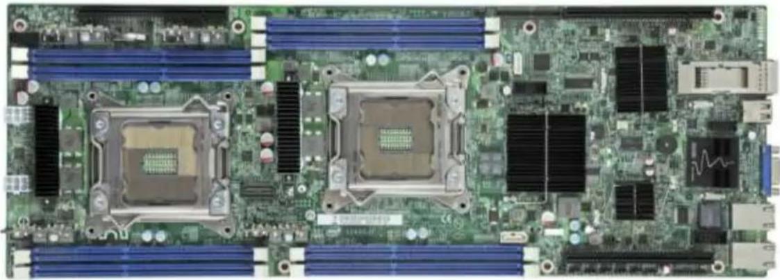
Top-down view of a computer motherboard with visible CPU socket and RAM slots (no text or symbols)Figure 1. Intel® Server Board S2600JF (InfiniBand* SKU)
There are three board SKUs based on different hardware configuration:
■ S2600JF: Base SKU
- S2600JFQ: Base SKU with InfiniBand* ConnectX-3* QDR populated
- S2600JFF: Base SKU with InfiniBand* ConnectX-3* FDR populated
The following table provides a high-level product feature list.
Table 1. Intel ^® Server Board S2600JF Feature Set
| Feature | Description |
| Processors | Support for one or two Intel® Xeon® Processor E5-2600 and E5-2600V2 series processors.Up to 8 GT/s Intel® QuickPath Interconnect (Intel® QPI)LGA 2011 Socket RThermal Design Power (TDP) up to 135 Watt |
| Memory | Eight DIMM slots total across eight memory channelsUnbuffered DDR3 and registered DDR3 with ECC DIMMsMemory DDR3 data transfer rates of 800/1066/1333/1600/1866 MT/sLoad Reduced DDR3 DIMMDDR3 standard I/O voltage of 1.5V (All Speed) and DDR3 Low Voltage of 1.35 V (1600 MT/s or below) |
| Chipset | Intel® C600-A Platform Controller Hub (PCH) with support for optional Storage Upgrade Key |
| External I/O Connections | DB-15 Video connectorsTwo RJ-45 Network Interfaces for 10/100/1000 LANOne stacked two-port USB 2.0 (Port 0/1) connectorOne InfiniBand* QDR QSFP port (SKU: S2600JFQ)One InfiniBand* FDR QSFP port (SKU: S2600JFF) |
| Internal I/O connectors/headers | Bridge Slot to extend board I/O○ SCU0 (Four SAS 3Gb/s ports) for backplane○ Front control panel signals○ One SATA (Port 0) 6Gb/s port for DOMOne USB 2.0 connector (USB port 2/3)One 2x7 pin header for system FAN moduleOne DH-10 serial Port A connectorOne SATA 6Gb/s (Port 1)One 2x4 pin header for Intel ^® RMM4 LiteOne 1x4 pin header for Storage Upgrade Key |
| Power Connections | Two sets of 2x3 pin connector |
| System Fan Support | Three sets of dual rotor fan |
| Add-in Riser Support | Three PCIe Gen III x16 riser slotsRiser slot 1 and 3 support PCIe Gen III x16 RiserRiser slot 2 supports PCIe Gen III x8 Riser (Intel ^® rIOM)One Bridge Slot for board I/O expansion |
| Video | Integrated 2D Video Graphics controller128 MB DDR2 Memory |
| Hard Drive Support | One SATA port at 6Gb/s on board. Four SATA/SAS ports (SCU0) and one SATA 6Gb/s port (for DOM) are supported through bridge board. |
| RAID Support | Intel ^® RSTe SW RAID 0/1/10/5 for SATA modeLSI* SW RAID 0/1/10/5 |
| Server Management | On-board ServerEngines* LLC Pilot III* ControllerSupport for Intel ^® Remote Management Module 4 Lite solutionsIntel ^® Light-Guided Diagnostics on field replaceable unitsSupport for Intel ^® System Management SoftwareSupport for Intel ^® Intelligent Power Node Manager (Need PMBus*-compliant power supply) |
2.1 Server Board Connector and Component Layout
The following illustration provides a general overview of the server board, identifying key feature and component locations. The majority of the items identified are common in the Intel® Server Board S2600JF family. The accompanying table identifies variations when present.
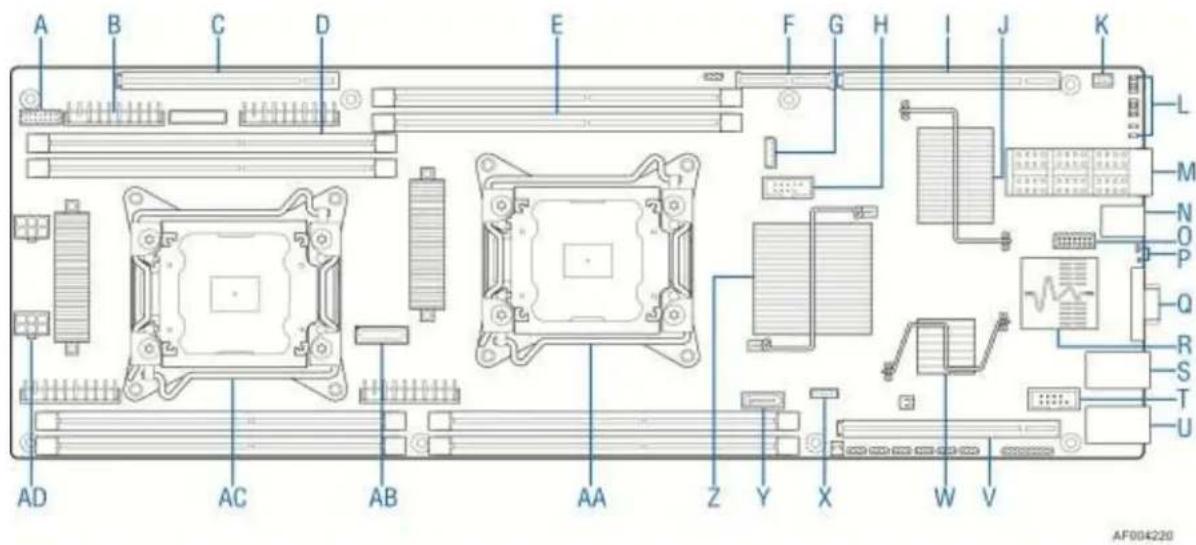
| A | 2x7 fan control connector | I | Riser Slot2 with PCIe Gen3 x16 | Q | VGA out | Y | SATA port 1 |
| B | VRS (4 total) | J | Infiniband* QDR or FDR | R | Dual port 1Gbe NIC | Z | PCH C600 |
| C | Riser Slot3 with PCIe Gen3 x16 | K | RMM4 lite | S | NIC Port 2 | AA | CPU 1 |
| D | CPU2 DIMM (4 total) | L | POST and QSFP LED | T | Serial Port A | AB | XDP connector |
| E | CPU1 DIMM (4 total) | M | QSFP | U | NIC Port 1 | AC | CPU 2 |
| F | Bridge board connector | N | USB x2 | V | Riser Slot1 with PCIe Gen3 x16 | AD | 2x3 PWR connector (2 total) |
| G | IPMB | O | Debug connector | W | Integrated BMC | ||
| H | 2x5 USB | P | Status and ID LED | X | Storage Upgrade key |
Figure 2. Intel ^® Server Board S2600JF Components
2.1.1 Board Rear Connector Placement
The Intel ^® Server Board S2600JF has the following board rear connector placement.

| Description | Description | ||
| A | NIC port 1 (RJ45) | E | Status LED |
| B | NIC port 2 (RJ45) | F | Dual port USB connector |
| C | DB15 video out | G | QSFP Connector |
| D | ID LED | H | IB status and Diagnostic LED |
Figure 3. Rear Panel Connector Placement
2.1.2 Server Board Mechanical Drawings
The following figure is a mechanical drawing for the Intel ^® Server Board S2600JF.
![12 [0.004] 6.33 [1.248] 28.8 [1.000] [4.34 [1.667] 24 [1.000] [7.236] [7.236] [7.236] [7.236] [7.236] [7.236] [7.236] [7.236] [7.236] [7.236] [7.236] [7.236] [7.236] [7.236] [7.236] 112.79 [4.438] 158.45 [8.248] 227.95 [8.679] 257.59 [18.141] 288 [11.339] 288.66 [11.798] 288.66 [14.514] 408 [15.748] 418.5 [18.398] 257.59 [18.141] 257.59 [18.141] 257.59 [18.141] 257.59 [18.141] 257.59 [18.141] 257.59 [18.141] 257.59 [18.141] 257.59 [20.000] 257.59 [20.000] 257.59 [20.000] 257.59 [20.000] 257.59 [20.000] 257.59 [20.000] 257.59 [20.000] 257.59 [19.339] [19.339] [19.339] [19.339] [19.339] [19.339] [19.339] [19.339] [19.339] [19.339] [19.339] [19.339] [19.339] [19, 87 (1, 328)] [19, 87 (1, 328)] [19, 87 (1, 328)] [19, 87 (1, 328)] [19, 87 (1, 328)] [19, 87 (1, 328)] [19, 87 (1, 328)] [19] 94 (1, 236) (1, 236) (1, 236) (1, 236) (1, 236) (1, 236) (1, 236) (1, 236) (1, 236) (1, 236) (1, 236) (1, 236) (1, 236) (1, -0.078) (1, -0.078) (1, -0.078) (1, -0.078) (1, -0.078) (1, -0.078) (1, -0.078) (1, -0.078) (1, -0.078) (1, -0.078) (1, -0.076) (1, -0.076) (1, -0.076) (1, -0.076) (1, -0.076) (1, -0.076) (1, -0.076) (1, -0.076) (1, -0.076) (1, -0.076) (1, -0.075) (1, -0.075) (1, -0.075) (1, -0.075) (1, -0.075) (1, -0.075) (1, -0.075) (1, -0.075) (1, -0.075) (1, -0.075) (1, -0.074) (1, -0.074) (1, -0.074) (1, -0.074) (1, -0.074) (1, -0.074) (1, -0.074) (1, -0.074) (1, -0.074) (1, -0.074) (1, -0.073) (1, -0.074) (1, -0.074) (1, -0.074) (1, -0.074) (1, -0.074) (1, -0.074) (1, -0.074) (1, -0.074) (1, -0.074) (1, -0.075) (1, -0.075) (1, -0.075) (1, -0.075) (1, -0.075) (1, -0.075) (1, -0.075) (1, -0.075) (1, -0.075) (1, -0.076) (1, -0.076) (1, -0.076) (1, -0.076) (1, -0.076) (1, -0.076) (1, -0.076) (1, -0.076) (1, -0.076) (1, -0.078)](/content/2026/05/920061/images/8d5b5bf1c7fecbfb93eeffa9ac16052940b347f56c748d330105078bf8fc22ed.jpg)
Figure 4. Baseboard and Mounting Holes
3. Product Architecture Overview
The Intel ^® Server Board S2600JF is a purpose-built, rack-optimized server board used in a high-density rack system. It is designed around the integrated features and functions of the Intel ^® Xeon ^® processor E5-2600 and E5-2600V2 product family, the Intel ^® C600-A chipset, and other supporting components including the Integrated BMC, the Intel ^® i350 network interface controller, and the Mellanox ^ ConnectX-3 ^ InfiniBand ^* (depending on the board SKU).
The reduced board size allows four boards reside in a standard multi-node 2U Intel ^® Server Chassis H2000JF for high performance and high density computing.
3.1 High Level Product Features
Table 2. Intel ^® Server Board S2600JF Features
| Board | S2600JF | S2600JFQ/S2600JFF |
| Form Factor | 6.4" (153mm) x 17.8" (453mm) | 6.4" (153mm) x 17.8" (453mm) |
| CPU Socket | Socket R and LGA 2011 | Socket R and LGA 2011 |
| Chipset | Intel® C600 Chipset PCH | Intel® C600 Chipset PCH |
| Memory | Eight DDR3 RDIMMs/LR-DIMMs/UDIMMs with ECC | Eight DDR3 RDIMMs/LR-DIMMs/UDIMMs with ECC |
| Slots | Three PCI Express* Gen3 x16 connectorsOne system bridge board connector | Three PCI Express* Gen3 x16 connectorsOne system bridge board connector |
| Ethernet | Dual GbE, Intel® I350 Gigabit Ethernet | Dual GbE, Intel® I350 Gigabit Ethernet |
| InfiniBand* | NA | Single port of InfiniBand* QDR/FDR |
| Storage | One SATA III port (6Gb/s) | One SATA III port (6Gb/s) |
| SAS | SCU0 through bridge board slot | SCU0 through bridge board slot |
| SW RAID | LSI* SW RAID 0,1,5,10 or RSTe RAID 0,1,5 for SATA mode | LSI* SW RAID 0,1,5,10 or RSTe RAID 0,1,5 for SATA mode |
| Processor Support | 135W maximum | 135W maximum |
| Video | Integrated in BMC | Integrated in BMC |
| iSMS | Integrated BMC w/IPMI 2.0 support | Integrated BMC w/IPMI 2.0 support |
| Chassis | H2000 family | H2000 family |
| Power Supply | 12V and 5VS/B PMBus* | 12V and 5VS/B PMBus* |
flowchart
graph TD
    subgraph_CPU_1["CPU 1"]
        A["Intel® Xeon® E5-2600 E5-2600V2"] <-->|QPI PORT 0: 8.0GT/s| B["Intel® Xeon® E5-2600 E5-2600V2"]
        C["CPU 2"] <-->|QPI PORT 1: 8.0GT/s| B
    end

    D["Intel® C600-A/B"] -->|PCI-E GEN2 x4 (4GB/s)| E["Server Engines PILOT 3 IBMC"]
    E --> F["PCI-E GEN1 x1"]
    E --> G["PCI-E GEN3 x16 (32GB/s)"]
    E --> H["PCI-E GEN3 x16 (32GB/s)"]
    E --> I["PCI-E GEN1 x16 (32GB/s)"]
    E --> J["PCI-E GEN3 x16 (32GB/s)"]
    E --> K["PCI-E GEN3 x16 (32GB/s)"]
    E --> L["PCI-E GEN3 x16 (32GB/s)"]
    E --> M["PCI-E GEN3 x16 (32GB/s)"]
    E --> N["PCI-E GEN3 x16 (32GB/s)"]
    E --> O["PCI-E GEN3 x16 (32GB/s)"]
    E --> P["PCI-E GEN3 x16 (32GB/s)"]
    E --> Q["PCI-E GEN3 x16 (32GB/s)"]
    E --> R["PCI-E GEN3 x16 (32GB/s)"]
    E --> S["PCI-E GEN3 x16 (32GB/s)"]
    E --> T["PCI-E GEN3 x16 (32GB/s)"]
    E --> U["PCI-E GEN3 x16 (32GB/s)"]
    E --> V["PCI-E GEN3 x16 (32GB/s)"]
    E --> W["PCI-E GEN3 x16 (32GB/s)"]
    E --> X["PCI-E GEN3 x16 (32GB/s)"]
    E --> Y["PCI-E GEN3 x16 (32GB/s)"]
    E --> Z["PCI-E GEN3 x16 (32GB/s)"]
    E --> AA["PCI-E GEN3 x16 (32GB/s)"]
    E --> AB["PCI-E GEN3 x16 (32GB/s)"]
    E --> AC["PCI-E GEN3 x16 (32GB/s)"]
    E --> AD["PCI-E GEN3 x16 (32GB/s)"]
    E --> AE["PCI-E GEN3 x16 (32GB/s)"]
    E --> AF["PCI-E GEN3 x16 (32GB/s)"]
    E --> AG["PCI-E GEN3 x16 (32GB/s)"]
    E --> AH["PCI-E GEN3 x16 (32GB/s)"]
    E --> AI["PCI-E GEN3 x16 (32GB/s)"]
    E --> AJ["PCI-E GEN3 x16 (32GB/s)"]
    E --> AK["PCI-E GEN3 x16 (32GB/s)"]
    E --> AL["PCI-E GEN3 x16 (32GB/s)"]
    E --> AM["PCI-E GEN3 x16 (32GB/s)"]
    E --> AN["PCI-E GEN3 x16 (32GB/s)"]
    E --> AO["PCI-E GEN3 x16 (32GB/s)"]
    E --> AP["PCI-E GEN3 x16 (32GB/s)"]
    E --> AQ["PCI-E GEN3 x16 (32GB/s)"]
    E --> AR["PCI-E GEN3 x16 (32GB/s)"]
    E --> AS["PCI-E GEN3 x16 (32GB/s)"]
    E --> AT["PCI-E GEN3 x16 (32GB/s)"]
    E --> AU["PCI-E GEN3 x16 (32GB/s)"]
    E --> AV["PCI-E GEN3 x16 (32GB/s)"]
    E --> AW["PCI-E GEN3 x16 (32GB/s)"]
    E --> AX["PCI-E GEN3 x16 (32GB/s)"]
    E --> AY["PCI-E GEN3 x16 (32GB/s)"]
    E --> AZ["PCI-E GEN3 x16 (32GB/s)"]
    E --> BA["PCI-E GEN3 x16 (32GB/s)"]
    E --> BB["PCI-E GEN3 x16 (32GB/s)"]
    E --> BC["PCI-E GEN3 x16 (32GB/s)"]
    E --> BD["PCI-E GEN3 x16 (32GB/s)"]
    E --> BE["PCI-E GEN3 x16 (32GB/s)"]
    E --> BF["PCI-E GEN3 x16 (32GB/s)"]
    E --> BG["PCI-E GEN3 x16 (32GB/s)"]
    E --> BH["PCI-E GEN3 x16 (32GB/s)"]
    E --> BI["PCI-E GEN3 x16 (32GB/s)"]
    E --> BJ["PCI-E GEN3 x16 (32GB/s)"]
    E --> BK["PCI-E GEN3 x16 (32GB/s)"]
    E --> BL["PCI-E GEN3 x16 (32GB/s)"]
    E --> BM["PCI-E GEN3 x16 (32GB/s)"]
    E --> BN["PCI-E GEN3 x16 (32GB/s)"]
    E --> BO["PCI-E GEN3 x16 (32GB/s)"]
    E --> BP["PCI-E GEN3 x16 (32GB/s)"]
    E --> BQ["PCI-E GEN3 x16 (32GB/s)"]
    E --> BR["PCI-E GEN3 x16 (32GB/s)"]
    E --> BS["PCI-E GEN3 x16 (32GB/s)"]
    E --> BT["PCI-E GEN3 x16 (32GB/s)"]
    E --> BU["PCI-E GEN3 x16 (32GB/s)"]
    E --> BV["PCI-E GEN3 x16 (32GB/s)"]
    E --> BW["PCI-E GEN3 x16 (32GB/s)"]
    E --> BX["PCI-E GEN3 x16 (32GB/s)"]
    E --> BY["PCI-E GEN3 x16 (32GB/s)"]
    E --> BZ["PCI-E GEN3 x16 (32GB/s)"]
    E --> CA["PCI-E GEN3 x16 (32GB/s)"]
    E --> CB["PCI-E GEN3 x16 (32GB/s)"]
    E --> CC["PCI-E GEN3 x16 (32GB/s)"]
    E --> CD["CLOCK LOGIC"]
    CD --> CE["CX400G"]
    CD --> CF["XB1900Z"]
    CD --> CG["CIOING+"]
    CE & CF & GD & BX & BY & BW & BX & BW & BX & BW & BX & BW & BX & BW & BX & BW & BX & BW & BX & BW & BX & BW & BX & BW & BX & BW & BX & BW & BX & BW & BX & BW & BX & BW & BX & BW & BX & BW & BX & BW & BX & BW & BX & BW & BX & BW & BX & BW & BX & BW & BX & BW & BX & BW & BX & BW & BU & BW & BW & BW & BW & BW & BW & BW & BW & BW & BW & BW & BW & BW & BW & BW & BW & BW & BW & BW & BW & BW & BW & BW & BW & BW & BW & BW & BW & BW & BW & BW & BW & BW & BW & BW & BW & BW & BW & BW & BW & BW & BW & BW & BW & BW & BW & BW & BW & BW & BW & BU & BW & BW & BW & BW & BW & BW & BW & BW & BW & BW & BW & BW & BW & BW & BW & BW & BW & BW & BW & BW & BW & BW & BW & BW & BW & BW & BW & BW & BW & BW & BW & BW & BW & BW & BW & BW & BW & BW & BW & BW & BW & BW & BW & BW & BW & BW & BW & BU & BW & BU & BW & BW & BW & BW & BW & BW & BW & BW & BW & BW & BW & BW & BW & BW & BW & BW & BW & BW & Bu & Bu & Bu & Bu / Dual 1Gb LAN / Dual 1Gb LAN / Dual 1Gb LAN / Dual 1Gb LAN / Dual 1Gb LAN / Dual 1Gb LAN / Dual 1Gb LAN / Dual 1Gb LAN / Dual 1Gb LAN / Dual 1Gb LAN / Dual 1Gb LAN / Dual 1Gb LAN / Dual 1Gb LAN / Dual 1Gb LAN / Dual 1Gb LAN / Dual 1Gb LAN / Dual 1Gb LAN / Dual 4Gb LAN / Dual 4Gb LAN / Dual 4Gb LAN / Dual 4Gb LAN / Dual 4Gb LAN / Dual 4Gb LAN / Dual 4Gb LAN / Dual 4Gb LAN / Dual 4Gb LAN / Dual 4Gb LAN / Dual 4Gb LAN / Dual 4Gb LAN / Dual 4Gb LAN / Dual 4Gb LAN / Dual 4Gb LAN / Dual 4Gb LAN / Dual 4Gb LAN / Multiclock |
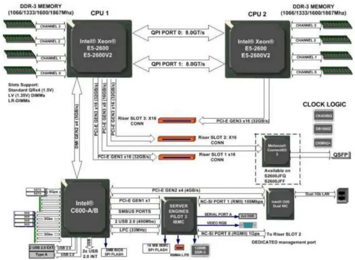
Figure 5. Intel ^® Server Board S2600JF Functional Block Diagram
3.2 Processor Support
The server board includes two Socket-R (LGA 2011) processor sockets and supports one or two of the Intel® Xeon® processor E5-2600 and E5-2600V2 product family, with a Thermal Design Power (TDP) of up to 135W processor.
The Intel® Xeon® E5-2600 and E5-2600V2 processor family are composed of up to 10/12 cores respectively. The microprocessors include an integrated DDR3 memory controller (IMC) with four memory channels that can support up to three ECC Registered DIMMs or three Unbuffered ECC DIMMs per memory channel, and an integrated I/O controller with 40 PCI Express* Gen3 lanes controlled by ten PCI Express* Master Controllers. The target TDPs are 80W, 95W, 115W, 130W, and 135W on Intel® Server Board S2600JF.
Previous generation Intel ^® Xeon ^® processors are not supported on the Intel ^® Server Boards described in this document.
For a complete updated list of supported processors, see: http://www.intel.com/p/en_US/support/highlights/server/sb-s2600jf.
On the Support tab, look for Compatibility and then Supported Processor List.
3.2.1 Processor Socket Assembly
Each processor socket of the server board is pre-assembled with an Independent Latching Mechanism (ILM) and Back Plate that allow for secure placement of the processor and processor heat to the server board.
The following illustration identifies each sub-assembly component.
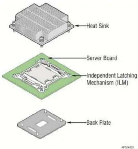
Figure 6. Processor Socket Assembly
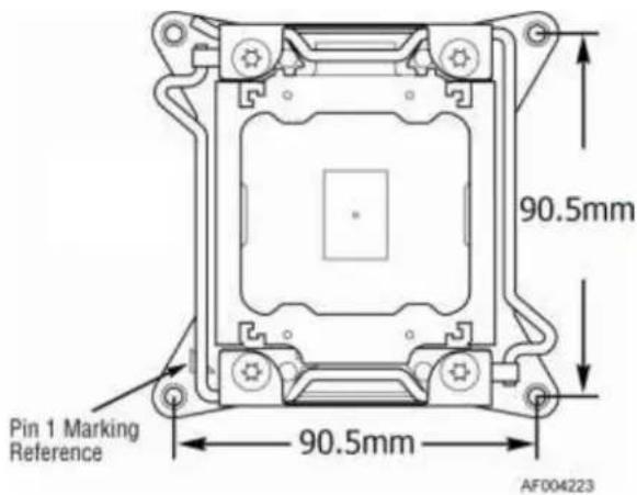
Figure 7. Processor Socket ILM Variations
The square ILM has a 90.5 x 90.5mm heat sink mounting hole pattern and is used on the Intel® Server Board S2600JF.
3.2.2 Processor Population Rules
Note: Although the server board does support dual-processor configurations consisting of different processors that meet the following defined criteria, Intel does not perform validation testing of this configuration. For optimal system performance in dual-processor configurations, Intel recommends that identical processors be installed.
When using a single-processor configuration, the processor must be installed into the processor socket labeled CPU_1.
When two processors are installed, the following population rules apply:
- Both processors must be of the same processor family.
- Both processors must have the same cache size.
- Processors with different speeds can be mixed in a system, given the prior rules are met. If this condition is detected, all processor speeds are set to the lowest common denominator (highest common speed) and an error is reported.
- Processor stepping within a common processor family can be mixed as long as it is listed in the processor specification updates published by Intel Corporation.
The following table describes mixed processor conditions and recommended actions for all Intel® Server Boards and Intel® Server Systems designed around the Intel® Xeon® processor E5-2600 product family and Intel® C600 chipset product family architecture. The errors fall into one of the following two categories:
- Fatal: If the system can boot, it goes directly to the Error Manager screen in BIOS Setup, regardless of whether the "POST Error Pause" setup option is enabled or disabled.
- Major: If the "POST Error Pause" option in BIOS Setup is disabled, the system logs the error to the BIOS Setup Utility Error Manager and then continues to boot. No POST error message is given. If the "POST Error Pause" option in BIOS Setup is enabled, the error is logged and the system goes directly to the Error Manager in BIOS Setup.
Table 3. Mixed Processor Configurations
| Error | Severity | System Action |
| Processor family not identical | Fatal | The BIOS detects the error condition and responds as follows:• Logs the error into the system event log (SEL).• Alerts the Integrated BMC of the configuration error with an IPMI command.• Does not disable the processor.• Displays “0194: Processor family mismatch detected” message in the error manager.• Halts the system. |
| Processor cache not identical | Fatal | The BIOS detects the error condition and responds as follows:• Logs the error into the SEL.• Alerts the Integrated BMC of the configuration error with an IPMI command.• Does not disable the processor.• Displays “0192: Cache size mismatch detected” message in the error manager.• Halts the system. |
| Processor frequency (speed) not identical | Major | The BIOS detects the error condition and responds as follows:• Adjusts all processor frequencies to the lowest common denominator.• Continues to boot the system successfully.If the frequencies for all processors cannot be adjusted to be the same, the BIOS:• Logs the error into the SEL.• Displays “0197: Processor speeds mismatched” message in the error manager.• Halts the system. |
| Processor microcode missing | Fatal | The BIOS detects the error condition and responds as follows:• Logs the error into the SEL.• Alerts the Integrated BMC of the configuration error with an IPMI command.• Does not disable processor.• Displays “816x: Processor 0x unable to apply microcode update” message in the error manager.• Pauses the system for user intervention. |
| Processor Intel® QuickPath Interconnect speeds not identical | Halt | The BIOS detects the error condition and responds as follows:• Logs the error into the SEL.• Alerts the Integrated BMC of the configuration error with an IPMI command.• Does not disable the processor.• Displays “0195: Processor Front Side Bus speed mismatch detected” message in the error manager.• Halts the system. |
Note: When a single processor is installed, no terminator is required in the second processor socket.
3.3 Processor Function Overview
With the release of the Intel ^® Xeon ^® processor E5-2600V2 product family, several key system components, including the CPU, Integrated Memory Controller (IMC), and Integrated IO Module (IIO), have been combined into a single processor package and feature per socket; two Intel ^® QuickPath Interconnect point-to-point links capable of up to 8.0 GT/s, up to 40 lanes of Gen 3 PCI Express ^ links capable of 8.0 GT/s, and four lanes of DMI2/PCI Express ^ Gen 2 interface with a peak transfer rate of 5.0 GT/s. The processor supports up to 46-bit physical address space and 48-bit virtual address space.
The following sections provide an overview of the key processor features and functions that help to define the performance and architecture of the server board. For more comprehensive processor-specific information, refer to the Intel ^® Xeon ^® processor E5-2600V2 product family documents listed in the Reference Documents section.
Processor Feature Details:
- Up to 12 execution cores (Intel ^ Xeon ^ processor E5-2600V2 only)
- Each core supports two threads (Intel ^ Hyper-Threading Technology), up to 24 threads per socket
- 46-bit physical addressing and 48-bit virtual addressing
■ 1-GB large page support for server applications - A 32-KB instruction and 32-KB data first-level cache (L1) for each core
- A 256-KB shared instruction/data mid-level (L2) cache for each core
- Up to 30-MB last level cache (LLC) and up to 2.5-MB per core instruction/data last level cache (LLC), shared among all cores
Supported Technologies:
Intel ^® Virtualization Technology (Intel ^® VT)
Intel ^® Virtualization Technology for Directed I/O (Intel ^® VT-d)
Intel ^® Virtualization: APIC Virtualization (APICv)
Intel ^® Virtualization Technology Xeon ^® E5-2600 Processor Extensions
Intel ^® Trusted Execution Technology (Intel ^® TXT)
Intel ^® 64 Architecture
Intel ^® Streaming SIMD Extensions 4.1 (Intel ^® SSE4.1)
Intel ^® Streaming SIMD Extensions 4.2 (Intel ^® SSE4.2)
Intel ^® Advanced Vector Extensions (Intel ^® AVX) Float 16
Intel ^® Hyper-Threading Technology
Intel ^® Node Manager – Basic and Extended Editions
- Execute Disable Bit
■ Max Memory Speed update to 1866 MT/s
Intel ^® Turbo Boost Technology
Intel ^® Intelligent Power Technology
■ Data Direct I/O (DDIO)
■ Enhanced Intel ^® SpeedStep Technology
- PCI express* Atomic operation, x16 Non-Transparent Bridge (NTB) (Intel ^ Xeon ^ processor E5-2600V2 only)
Intel ^® 64 OS Guide
Intel ^® 64 Secure Key
3.3.1 Intel \* QuickPath Interconnect
The Intel ^® QuickPath Interconnect is a high-speed, packetized, point-to-point interconnect used in the processor. The narrow high-speed links stitch together processors in distributed shared memory and integrated I/O platform architecture. It offers much higher bandwidth with low latency. The Intel ^® QuickPath Interconnect has an efficient architecture allowing more interconnect performance to be achieved in real systems. It has a snoop protocol optimized for low latency and high scalability, as well as packet and lane structures enabling quick completions of transactions. Reliability, Availability, and Serviceability features (RAS) are built into the architecture.
The physical connectivity of each interconnect link is made up of twenty differential signal pairs plus a differential forwarded clock. Each port supports a link pair consisting of two unidirectional links to complete the connection between two components. This supports traffic in both directions simultaneously. To facilitate flexibility and longevity, the interconnection is defined as having five layers: Physical, Link, Routing, Transport, and Protocol.
The Intel ^® QuickPath Interconnect includes a cache coherency protocol to keep the distributed memory and caching structures coherent during system operation. It supports both low-latency source snooping and a scalable home snoop behavior. The coherency protocol provides for direct cache-to-cache transfers for optimal latency.
3.3.2 Integrated Memory Controller (IMC) and Memory Subsystem
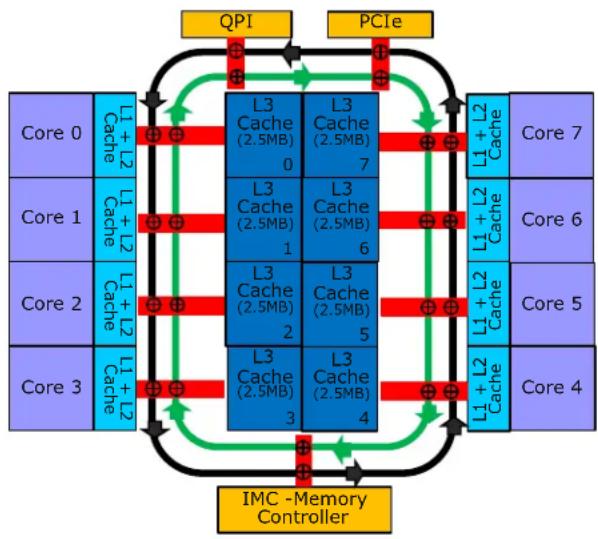
flowchart
graph TD
    subgraph Core_0
        A["Core 0"] --> B["L1 + L2 Cache"]
        C["Core 1"] --> D["L1 + L2 Cache"]
        E["Core 2"] --> F["L1 + L2 Cache"]
        G["Core 3"] --> H["L1 + L2 Cache"]
    end

    subgraph Core_1
        I["Core 1"] --> J["L1 + L2 Cache"]
        K["Core 2"] --> L["L1 + L2 Cache"]
        M["Core 3"] --> N["L1 + L2 Cache"]
    end

    subgraph Core_2
        O["Core 2"] --> P["L1 + L2 Cache"]
        Q["Core 3"] --> R["L1 + L2 Cache"]
        S["Core 4"] --> T["L1 + L2 Cache"]
    end

    subgraph Core_3
        U["Core 3"] --> V["L1 + L2 Cache"]
        W["Core 4"] --> X["L1 + L2 Cache"]
    end

    subgraph IMC -Memory Controller
        Y["QPI"] --> Z["L3 Cache (2.5MB) 0"]
        Y --> AA["L3 Cache (2.5MB) 1"]
        Y --> AB["L3 Cache (2.5MB) 2"]
        Y --> AC["L3 Cache (2.5MB) 3"]
        Y --> AD["L3 Cache (2.5MB) 4"]
    end

    subgraph PCIe
        AE["PCIe"] --> AF["L1 + L2 Cache"]
        AE --> AG["L1 + L2 Cache"]
        AE --> AH["L1 + L2 Cache"]
        AE --> AI["L1 + L2 Cache"]
    end

    A --> J --> K --> M --> U
    B --> J --> K --> M --> U
    D --> J --> K --> M --> U
    F --> J --> K --> M --> U
    W --> J --> K --> M --> U
    Y --> AA --> AB --> AC --> AD
    AE --> AF --> AG --> AH --> AI
Figure 8. Processor with IMC Functional Block Diagram
- Unbuffered DDR3 and registered DDR3 DIMMs.
-
LR DIMM (Load Reduced DIMM) for buffered memory solutions demanding higher capacity memory subsystems.
-
Independent channel mode or lockstep mode.
- Data burst length of eight cycles for all memory organization modes.
■ Memory DDR3 data transfer rates of 800, 1066, 1333, 1600, and 1867 MT/s. - 64-bit wide channels plus 8-bit ECC support for each channel.
- DDR3 standard I/O Voltage of 1.5V for all speed.
- DDR3 Low Voltage of 1.35V for 1600MT/s or below.
-
1Gb, 2Gb, and 4Gb DDR3 DRAM technologies supported for these devices:
-
UDIMM DDR3 – SR x8 and x16 data widths, DR – x8 data width.
- RDIMM DDR3 – SR, DR, and QR – x4 and x8 data widths.
-
LRDIMM DDR3 – QR – x4 and x8 data widths with direct map or with rank multiplication.
-
Up to eight ranks supported per memory channel, 1, 2, or 4 ranks per DIMM.
- Open with adaptive idle page close timer or closed page policy.
- Per channel memory test and initialization engine can initialize DRAM to all logical zeros with valid ECC (with or without data scrambler) or a predefined test pattern.
- Isochronous access support for Quality of Service (QoS).
- Minimum memory configuration: Independent channel support with one DIMM populated.
- Integrated dual SMBus* master controllers.
- Command launch modes of 1n/2n.
-
RAS Support:
-
Rank Level Sparing and Device Tagging.
o Demand and Patrol Scrubbing. - DRAM Single Device Data Correction (SDDC) for any single x4 or x8 DRAM device. Independent channel mode supports x4 SDDC. The x8 SDDC requires lockstep mode.
- Lockstep mode where channels 0 and 1 and channels 2 and 3 are operated in lockstep mode.
○ Data scrambling with address to ease detection of write errors to an incorrect address. - Error reporting through Machine Check Architecture.
- Read Retry during CRC error handling checks by iMC.
○ Channel mirroring within a socket. - CPU1 Channel Mirror Pairs (A, B) and (C, D).
- CPU2 Channel Mirror Pairs (E, F) and (G, H).
- Error Containment Recovery.
- Improved Thermal Throttling with dynamic Closed Loop Thermal Throttling (CLTT).
- Memory thermal monitoring support for DIMM temperature.
3.3.2.1 Supported Memory
Table 4. Color Definition
| Supported and Validated | |
| Supported but not Validate | |
| TBD |
Table 5. UDIMM Support Guidelines
| Ranks Per DIMM and Data Width | Memory Capacity Per DIMM1 | Speed (MT/s) and Voltage Validated by Slot per Channel (SPC) and DIMM Per Channel (DPC) ^2,3 | |||
| 1 Slot per Channel | |||||
| 1DPC | |||||
| 1.35V | 1.5V | ||||
| SRx8 ECC | 1GB | 2GB | 4GB | 1066, 1333, 1600^4 | 1066, 1333, 1600, 1867 ^4 |
| DRx8 ECC | 2GB | 4GB | 8GB | 1066, 1333, 1600^4 | 1066, 1333, 1600, 1867 ^4 |
Notes:
- Supported DRAM Densities are 1Gb, 2Gb, and 4Gb. Only 2Gb and 4Gb are validated by Intel.
- Command Address Timing is 1N for 1DPC and 2N for 2DPC.
- No support for 3DPC when using UDIMMs.
- These speed options are only available when "Memory SPD Override" is enabled.
Table 6. RDIMM Support Guidelines
| Ranks Per DIMM and Data Width | Memory Capacity Per DIMM1 | Speed (MT/s) and Voltage Validated by Slot per Channel (SPC) and DIMM Per Channel (DPC) ^2 | |||
| 1 Slot per Channel | |||||
| 1DPC | |||||
| 1.35V | 1.5V | ||||
| SRx8 | 1GB | 2GB | 4GB | 1066, 1333, 1600 ^3 | 1066, 1333, 1600, 1867 ^3 |
| DRx8 | 2GB | 4GB | 8GB | 1066, 1333, 1600 ^3 | 1066, 1333, 1600, 1867 ^3 |
| SRx4 | 2GB | 4GB | 8GB | 1066, 1333, 1600 ^3 | 1066, 1333, 1600, 1867 ^3 |
| DRx4 | 4GB | 8GB | 16GB | 1066, 1333, 1600 ^3 | 1066, 1333, 1600, 1867 ^3 |
| QRx4 | 8GB | 16GB | 32GB | 800 | 1066 |
| QRx8 | 4GB | 8GB | 16GB | 800 | 1066 |
Notes:
- Supported DRAM Densities are 1Gb, 2Gb, and 4Gb. Only 2Gb and 4Gb are validated by Intel.
- Command Address Timing is 1N.
- These speed options are only available when "Memory SPD Override" is enabled.
Table 7. LRDIMM Support Guidelines
| Ranks Per DIMM and Data Width1 | Memory Capacity Per DIMM2 | Speed (MT/s) and Voltage Validated by Slot per Channel (SPC) and DIMM Per Channel (DPC)3,4,5 | ||
| 1 Slot per Channel | ||||
| 1DPC | ||||
| 1.35V | 1.5V | |||
| QRx4 (DDP)6 | 16GB | 32GB | 1066, 1333, 1600 | 1066, 1333, 1600, 1866 |
| 8Rx4 (QPP)6 | 32GB | 64GB | 1066 | 1066 |
Notes:
- Physical Rank is used to calculate DIMM Capacity.
- Supported and validated DRAM Densities are 2Gb and 4Gb.
- Command Address Timing is 1N.
- The speeds are estimated targets and verified through simulation.
- For 3SPC/3DPC - Rank Multiplication (RM) >=2.
- DDP – Dual Die Package DRAM stacking. P – Planar monolithic DRAM Dies.
3.3.2.2 Memory Population Rules
Note: Although mixed DIMM configurations may be supported by the chipset, Intel only performs platform validation on systems that are configured with identical DIMMs installed.
Each processor provides four banks of memory, each capable of supporting up to three DIMMs.
- DIMMs are organized into physical slots on DDR3 memory channels that belong to processor sockets.
- The memory channels from processor socket 1 are identified as Channel A, B, C, and D. The memory channels from processor socket 2 are identified as Channel E, F, G, and H.
- The silk screened DIMM slot identifiers on the board provide information about the channel, and therefore the processor to which they belong. For example, DIMM_A1 is the first slot on Channel A on processor 1; DIMM_E1 is the first DIMM socket on Channel E on processor 2.
- The memory slots associated with a given processor are unavailable if the corresponding processor socket is not populated.
- A processor may be installed without populating the associated memory slots provided a second processor is installed with associated memory. In this case, the memory is shared by the processors. However, the platform suffers performance degradation and latency due to the remote memory.
- Processor sockets are self-contained and autonomous. However, all memory subsystem support (such as Memory RAS and Error Management) in the BIOS setup is applied commonly across processor sockets.
On the Intel ^® Server Board S2600JF, a total of eight DIMM slots is provided (Two CPUs – four Channels/CPU and one DIMMs/Channel). The nomenclature for DIMM sockets is detailed in the following table.
Table 8. Intel ^® Server Board S2600JF DIMM Nomenclature
| Processor Socket 1 | Processor Socket 2 | ||||||
| (0)Channel A | (1)Channel B | (2)Channel C | (3)Channel D | (0)Channel E | (1)Channel F | (2)Channel G | (3)Channel H |
| A1 | B1 | C1 | D1 | E1 | F1 | G1 | H1 |
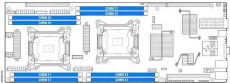
Figure 9. Intel ^® Server Board S2600JF Family DIMM Slot Layout
The following are generic DIMM population requirements that generally apply to the Intel ^® Server Board S2600JF:
- All DIMMs must be DDR3 DIMMs.
- Unbuffered DIMMs can be ECC only.
- Mixing of Registered and Unbuffered DIMMs is not allowed per platform.
- Mixing of LRDIMM with any other DIMM type is not allowed per platform.
- Mixing of DDR3 voltages is not validated within a socket or across sockets by Intel. If 1.35V (DDR3L) and 1.50V (DDR3) DIMMs are mixed, the DIMMs run at 1.50V.
- Mixing of DDR3 operating frequencies is not validated within a socket or across sockets by Intel. If DIMMs with different frequencies are mixed, all DIMMs run at the common lowest frequency.
- Quad rank RDIMMs are supported but not validated by Intel.
- A maximum of eight logical ranks (ranks seen by the host) per channel is allowed.
3.3.2.3 Publishing System Memory
- The BIOS displays the "Total Memory" of the system during POST if Display Logo is disabled in the BIOS setup. This is the total size of memory discovered by the BIOS during POST, and is the sum of the individual sizes of installed DDR3 DIMMs in the system.
- The BIOS displays the "Effective Memory" of the system in the BIOS setup. The term Effective Memory refers to the total size of all DDR3 DIMMs that are active (not disabled) and not used as redundant units.
- The BIOS provides the total memory of the system in the main page of the BIOS setup. This total is the same as the amount described by the first bullet above.
- If Display Logo is disabled, the BIOS displays the total system memory on the diagnostic screen at the end of POST. This total is the same as the amount described by the first bullet above.
3.3.2.4 RAS Features
The server board supports the following memory RAS modes:
■ Independent Channel Mode
- Rank Sparing Mode
- Mirrored Channel Mode
- Lockstep Channel Mode
Regardless of RAS mode, the requirements for populating within a channel given in the Memory Population Rules must be met at all times. Note that support of RAS modes that require matching DIMM population between channels (Mirrored and Lockstep) requires that ECC DIMMs be populated.
For RAS modes that require matching populations, the same slot positions across channels must hold the same DIMM type with regards to size and organization. DIMM timings do not have to match but timings will be set to support all DIMMs populated (that is, DIMMs with slower timings force faster DIMMs to the slower common timing modes).
3.3.2.4.1 Independent Channel Mode
Channels can be populated in any order in Independent Channel Mode. All four channels may be populated in any order and have no matching requirements. All channels must run at the same interface frequency but individual channels may run at different DIMM timings (RAS latency, CAS Latency, and so on).
3.3.2.4.2 Rank Sparing Mode
In Rank Sparing Mode, one rank is a spare of the other ranks on the same channel. The spare rank is held in reserve and is not available as system memory. The spare rank must have identical or larger memory capacity than all the other ranks (sparing source ranks) on the same channel. After sparing, the sparing source rank will be lost.
3.3.2.4.3 Mirrored Channel Mode
In Mirrored Channel Mode, the memory contents are mirrored between Channel 0 and Channel 2 and also between Channel 1 and Channel 3. As a result of the mirroring, the total physical memory available to the system is half of what is populated. Mirrored Channel Mode requires that Channel 0 and Channel 2, and Channel 1 and Channel 3 must be populated identically with regards to size and organization. DIMM slot populations within a channel do not have to be identical but the same DIMM slot location across Channel 0 and Channel 2 and across Channel 1 and Channel 3 must be populated the same.
3.3.2.4.4 Lockstep Channel Mode
In Lockstep Channel Mode, each memory access is a 128-bit data access that spans Channel 0 and Channel 1, and Channel 2 and Channel 3. Lockstep Channel mode is the only RAS mode that allows SDDC for x8 devices. Lockstep Channel Mode requires that Channel 0 and Channel 1, and Channel 2 and Channel 3 must be populated identically with regards to size and organization. DIMM slot populations within a channel do not have to be identical but the same
DIMM slot location across Channel 0 and Channel 1 and across Channel 2 and Channel 3 must be populated the same.
3.3.3 Processor Intergrated I/O Module (I/O)
The processor's integrated I/O module provides features traditionally supported through chipset components. The integrated I/O module provides the following features:
- PCI Express* Interfaces: The integrated I/O module incorporates the PCI Express* interface and supports up to 40 lanes of PCI Express*. Following are key attributes of the PCI Express* interface:
o Gen3 speeds at 8 GT/s (no 8b/10b encoding)
○ X16 interface bifurcated down to two x8 or four x4 (or combinations)
○ X8 interface bifurcated down to two x4
- DMI2 Interface to the PCH: The platform requires an interface to the legacy Southbridge (PCH) which provides basic, legacy functions required for the server platform and operating systems. Because only one PCH is required and allowed for the system, any sockets that do not connect to PCH will use this port as a standard x4 PCI Express* 2.0 interface.
- Integrated IOAPIC: Provides support for PCI Express* devices implementing legacy interrupt messages without interrupt sharing.
- Non-Transparent Bridge: PCI Express* Non-Transparent Bridge (NTB) acts as a gateway that enables high performance, low overhead communication between two intelligent subsystems, the local and the remote subsystems. The NTB allows a local processor to independently configure and control the local subsystem, and provides isolation of the local host memory domain from the remote host memory domain while enabling status and data exchange between the two domains.
- Intel ^ QuickData Technology: Used for efficient, high bandwidth data movement between two locations in memory or from memory to I/O.
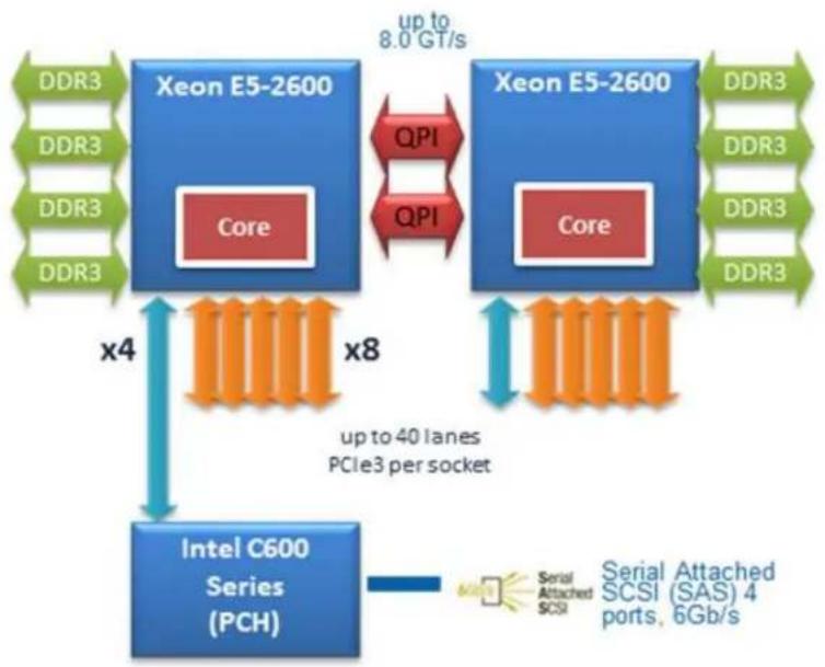
flowchart
graph TD
    A["Xeon E5-2600 Core"] -->|QPI| B["Xeon E5-2600 Core"]
    B -->|up to 8.0 GT/s| A
    A -->|x4| C["Intel C600 Series (PCH)"]
    B -->|x8| C
    C --> D["Serial Attached SCSI"]
    D --> E["Serial Attached SCSI (SAS) 4 ports, 6Gb/s"]
    style A fill:#f9f,stroke:#333
    style B fill:#bbf,stroke:#333
    style C fill:#bfb,stroke:#333
    style D fill:#ffb,stroke:#333
    style E fill:#fff,stroke:#333
Figure 10. General Functional Block Diagram of Processor I/O Subsystem
The following sub-sections describe the server board features that are directly supported by the processor IIO module. These include the Riser Card Slots, Network Interface, and connectors for the optional I/O modules and SAS Module. Features and functions of the Intel® C600 Series chipset are described in its own dedicated section.
3.3.3.1 Riser Card Support
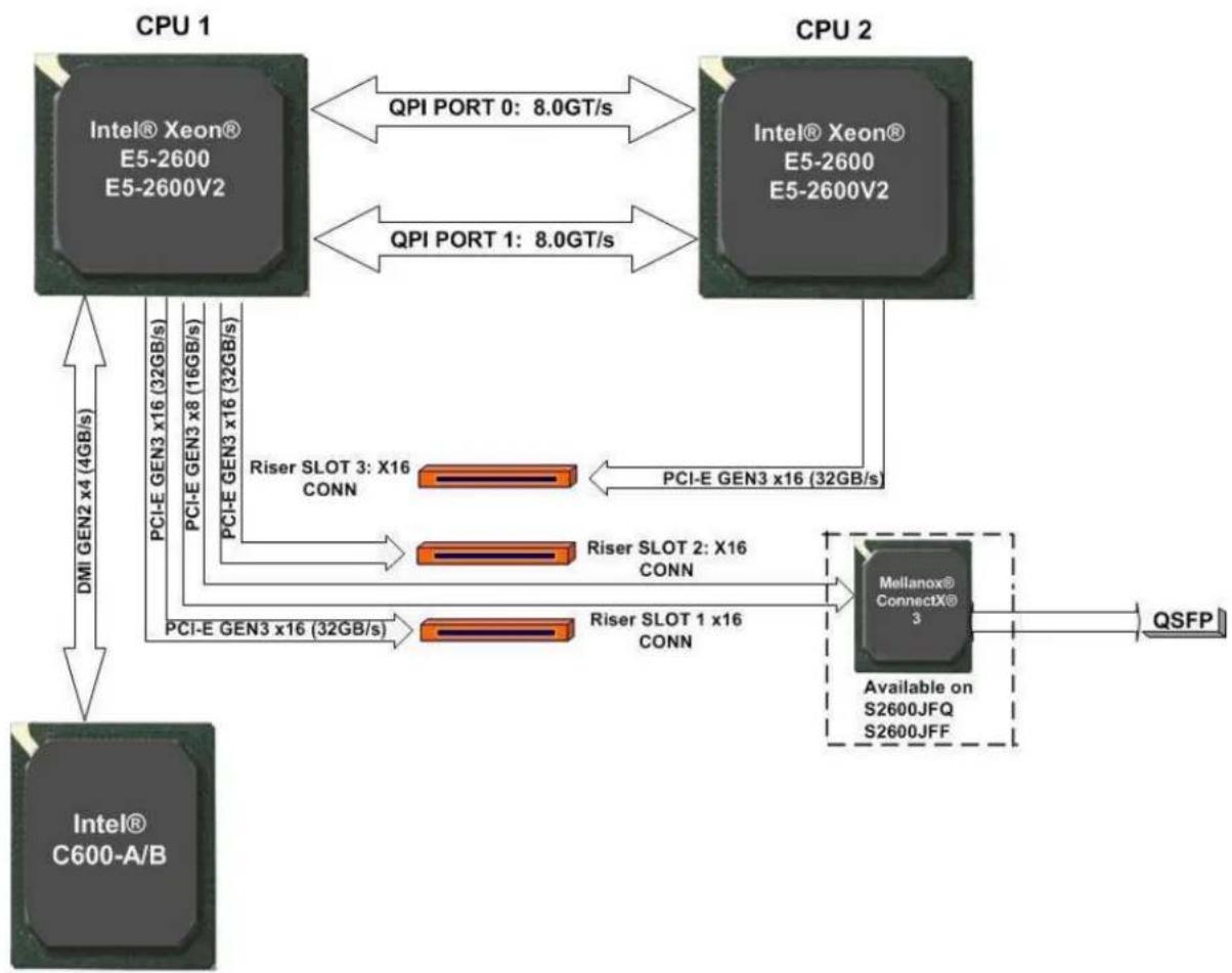
The server board provides three riser card slots identified by Riser Slot 1, Riser Slot 2, and Riser Slot 3. The PCIe signals for each riser card slot are supported by each of the two installed processors. A total of 32 PCIe Gen3 signals are routed to Riser Slot 1 and Riser Slot 2; all 32 lanes are routed from CPU 1. A total of 16 PCIe Gen3 signals are routed to Riser Card 3; all 16 lanes are routed from CPU 2.
Following is the scope of I/O connection from processors on Intel ^® Server Board S2600JF.
flowchart
graph TD
    A["Intel® C600-A/B"] -->|DMI GEN2 x4 (4GB/s)| B["CPU 1"]
    B -->|PCI-E GEN3 x16 (32GB/s)| C["CPU 2"]
    C -->|QPI PORT 0: 8.0GT/s| D["Intel® Xeon® E5-2600 E5-2600V2"]
    C -->|QPI PORT 1: 8.0GT/s| E["Intel® Xeon® E5-2600 E5-2600V2"]
    B -->|PCI-E GEN3 x8 (16GB/s)| F["Riser SLOT 3: X16 CONN"]
    C -->|PCI-E GEN3 x16 (32GB/s)| G["Riser SLOT 2: X16 CONN"]
    B -->|PCI-E GEN3 x16 (32GB/s)| H["Riser SLOT 1 x16 CONN"]
    C -->|PCI-E GEN3 x16 (32GB/s)| I["Mellanox® ConnectX® 3"]
    I --> J["Available on S2600JFQ S2600JFF"]
    I --> K["QSFP"]
Figure 11. PCI Express* Lane Distribution Scheme
Table 9. CPU1 and CPU2 PCIe Connectivity
| CPU | Port | IOU | Width | Connection |
| CPU1 | DMI2 | IOU2 | x4 | PCH (lane reversal, no polarity inversion) |
| CPU1 | PE1 | IOU2 | X8 | QDR/FDR InfiniBand* |
| CPU1 | PE2 | IOU0 | x16 | Riser 1 |
| CPU1 | PE3 | IOU1 | x16 | Riser 2 (x8 for IOM on Riser) |
| CPU2 | DMI2 | IOU2 | x4 | Unused |
| CPU2 | PE1 | IOU2 | x8 | Unused |
| CPU2 | PE2 | IOU0 | x16 | Unused |
| CPU2 | PE3 | IOU1 | x16 | Riser 3 |
Note: All riser slots are defined specially for dedicated risers only. Plugging in normal PCIe riser or PCIe add-in card directly causes danger and may burn out the add-in riser or card.
Riser Slot 3 can only be used in dual-processor configurations. Without the second processor installed, any graphic add-in card in Riser Slot 3 cannot output video, meaning the default video out is still from on-board integrated BMC.
3.3.3.2 Riser Types
The riser connector is a standard 164-pin x16 connector but pinned out differently to create enough unused pins to route the RGMII interface through Riser 2. It has an x16 PCIe Gen 3 electrical interface, which can be configured as 2 x8 if required. The placement of the rear IO connectors and layout of the components on the board must be made to support an MD2, low profile card in the Riser1 and an rIOM mounted on a riser carrier for Riser 2. Riser 3 on S2600JF supports off-board standard full height, full length I/O cards including double wide GPU boards.
To support GPU boards, each riser need to provide 66W of 12V power as well as 10W of 3.3V power in the case of 2 x8 boards being hosted in customized chassis. These risers need to generate 20W of 3.3V, the number of 12amp pins on the riser having increased to accommodate this.
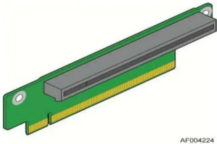
Supported 1U riser cards include:
- 1U Riser for slot 1 with one PCIe slot – x16 signals routed to an x16 PCIe Slot.
natural_image
3D rendering of a green and yellow electronic component with a gray internal structure (no text or symbols)Figure 12. PCIe Riser for Slot 1
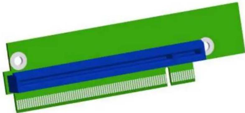
- 1U Riser for Slot 2 with one PCIe slot – 2 sets of x8 signals routed to an x16 PCIe Slot (eight lanes for IOM Carrier).
natural_image
3D rendered diagram of a mechanical component with green and blue parts, no text or symbols visibleFigure 13. PCIe Riser for Slot 2
- 1U customized Riser for Slot 2 with one PCIe slot – 1 set of x8 signals routed to root port 3A of processor 1 to facilitate Non-Transparent Bridge. For more information, refer to Multi-node Server Board Developers Spec under NDA.
3.3.3.3 Network Interface
Network connectivity from processor is provided by means of an on-board Mellanox*ConnectX-3* InfiniBand* Controller on board SKU S2600JFQ and S2600JFF, providing one SDR/DDR/QDR/FDR InfiniBand* port in a QSFP interface. The controller is supported by implementing x16 PCIe Gen3 signals from the IIO module of the CPU 1 processor.
3.3.3.4 I/O Module Support
To broaden the standard on-board feature set, the server board supports the option of adding a single I/O module providing external ports for a variety of networking interfaces. The I/O module attaches to a high density 80-pin connector of I/O module carrier on the Riser 2. Refer to Intel® Server System H2000JF Technical Product Specification (Intel Order Number G39462) for more information.
Intel ^® Xeon Phi ^™ Coprocessor Card – System Configuration Requirements For best system performance and proper fan speed control, ensure the system is configured as follows:
- The minimum system software revisions installed must be:
- System BIOS 01.06.0002 or later
○ BMC Firmware 01.17.4207 or later - FRUSDR 1.07 or later
Intel highly recommends that the latest available system software be installed. The latest system update package can be downloaded from the Intel website: http://www.intel.com/support
- The following
- MMIO over 4GB = Enabled
○ MMIO Size = 256GB
3.4 Intel °C600-A/B PCH Functional Overview
The following sub-sections provide an overview of the key features and functions of the Intel® C600-A/B chipset used on the server board. For more comprehensive chipset-specific information, refer to the Intel® C600 Series chipset documents listed in the Reference Documents section.
flowchart
graph LR
    A["SATA"] -->|6Gps| B["Intel® C600-A/B"]
    C["SATA"] -->|3Gps| B
    D["SAS"] -->|2 USB 2.0 EXT Type A| B
    E["SAS"] -->|USB 2.0| B
    F["SAS"] -->|USB 2.0| B
    G["SAS"] -->|USB 2.0| B
    H["SAS"] -->|USB 2.0| B
    I["PCI-E GEN1 x1 SMBUS PORTS 2 USB 2.0 (480Mbs) LPC (33MHz)"] --> B
    J["Server Engines PILOT 3 IBMC"] --> B
    K["NC-SI PORT 1 (RMII) 100Mbps"] --> L["Intel® I350 Dual NIC"]
    M["SERIAL PORT A"] --> N["2x5 HDR"]
    O["VIDEO RGB"] --> P["+"]
    Q["NC-SI PORT 0 (RGMII) 1Gps"] --> R["To PCIe SLOT 2"]
    S["DEDICATED management port"] --> T["16 MB IBMC SPI FLASH"]
    U["RMM4 LITE"] --> V["128MB DDR-3"]
    W["16 MB IBMC SPI FLASH"] --> X["128MB DDR-3"]
    Y["128MB DDR-3"] --> Z["16 MB IBMC SPI FLASH"]
    style B fill:#f9f,stroke:#333
    style I fill:#ccf,stroke:#333
    style K fill:#ccf,stroke:#333
    style L fill:#ccf,stroke:#333
    style M fill:#ccf,stroke:#333
    style Q fill:#ccf,stroke:#333
    style W fill:#ccf,stroke:#333
    style Y fill:#ccf,stroke:#333
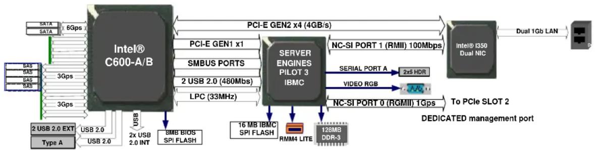
Figure 14. Intel ^® C600-A/B PCH Connection
The Intel ^® C600-A PCH component provides extensive I/O support. Functions and capabilities include:
- PCI Express* Base Specification, Revision 2.0, supports up to eight ports with transfers up to 5 GT/s
- PCI Local Bus Specification, Revision 2.3, supports 33 MHz PCI operations (supports up to four Req/Gnt pairs)
- ACPI Power Management Logic Support, Revision 4.0a
- Enhanced DMA controller, interrupt controller, and timer functions
- Integrated Serial Attached SCSI host controllers at transfer rate up to 3Gb/s on up to eight ports
- Integrated Serial ATA host controllers with independent DMA operation on up to six ports
- USB host interface with two EHCI high-speed USB 2.0 Host controllers and two rate matching hubs supporting up to 14 USB 2.0 ports
-
Integrated 10/100/1000 Gigabit Ethernet MAC with System Defense
-
System Management Bus (SMBus*) Specification, Version 2.0, with additional support for I²C devices
■ Supports Intel ^® High Definition Audio - Supports Intel ^ Rapid Storage Technology (Intel ^ RST)
- Supports Intel ^ Virtualization Technology for Directed I/O (Intel ^ VT-d)
- Supports Intel ^ Trusted Execution Technology (Intel ^ TXT)
- Low Pin Count (LPC) interface
- Firmware Hub (FWH) interface support
- Serial Peripheral Interface (SPI) support
- Intel ^ Anti-Theft Technology (Intel ^ AT)
- JTAG Boundary Scan support
3.4.1 PCI Express\*
The Intel ^® C600 PCH provides up to eight PCI Express* Root Ports, supporting the PCI Express* Base Specification, Revision 3.0. Each Root Port x1 lane supports up to 5Gb/s bandwidth in each direction (10Gb/s concurrent). PCI Express* Root Ports 1-4 or Ports 5-8 can independently be configured to support four x1s, two x2s, one x2 and two x1s, or one x4 port widths.
From PCH on the Intel ^® Server Board S2600JF, PCIe Port8 x1 Gen2 is connected to BMC Gen1 Uplink. Ports 1-4 are connected to the Intel ^® I350 GbE NIC. The remaining PCIe Gen2 interconnect (Port 5-7, 1 based numbering) are unused.
3.4.2 Non-Transparent Bridge
PCI Express* Non-Transparent Bridge (NTB) acts as a gateway that enables high performance, low overhead communication between two intelligent subsystems, the local and the remote subsystems. The NTB allows a local processor to independently configure and control the local subsystem, and provides isolation of the local host memory domain from the remote host memory domain while enabling status and data exchange between the two domains.
The PCI Express* Port 3A of the Intel® Xeon® Processor E5-2600 product family can be configured to be a transparent bridge or an NTB with x4/x8 link width and Gen1/Gen2/Gen3 link speed. Also this NTB port can be attached to another NTB port or PCI Express* Root Port on another subsystem. NTB supports three 64-bit BARs as configuration space or prefetchable memory windows that can access both 32-bit and 64-bit address space through 64-bit BARs.
There are three NTB-supported configurations:
- NTB Port to NTB Port Based Connection (Back-to-Back)
- NTB Port to Root Port Based Connection – Symmetric Configuration. The NTB port on the first system is connected to the root port of the second system. The second system's NTB port is connected to the root port on the first system making this a fully symmetric configuration.
- NTB Port to Root Port Based Connection – Non-Symmetric Configuration. The root port on the first system is connected to the NTB port of the second system. And it is not necessary for the first system to be of the Intel® Xeon® Processor E5-2600 product family.
3.4.3 Universal Serial Bus (USB)
There are 14 USB 2.0 ports available from Intel ^® C600 PCH. All ports are high-speed, full-speed and low-speed capable. A total of five USB 2.0 dedicated ports are used by Intel ^® Server Board S2600JF. The USB port distribution is as follows:
- ServerEngines* BMC PILOT III consumes two USB 2.0 ports (one USB 1.1 and one USB 2.0).
- Two rear USB 2.0 ports.
- One internal USB port for extension of front panel USB port.
- Wake on USB is supported on the rear and front panel USB ports for S1 only. Standby power on USB ports is not required.
3.4.4 Serial Attached SCSI (SAS) and Serial ATA (SATA) Controller
The Intel ^® C600-A/B chipset provides storage support through two integrated controllers: AHCI and SCU. By default, the server board supports up to six SATA ports: two single 6Gb/s SATA ports routed from the AHCI controller to one blue SATA connector labeled “SATA-1” on mother board and “SATA-1” on bridge board, and four 3Gb/s SATA ports routed from the SCU to the multi-drive port connector labeled “SAS/SATA 0-3” (grouped as SCU0).
Note: The multi-drive port connector labeled "SAS/SATA 4-7" is NOT functional by default and is enabled only with the addition of an Intel® RAID C600 Storage Upgrade Key option supporting eight SAS/SATA ports.
It supports the Serial ATA Specification, Revision 3.0, and several optional sections of the Serial ATA II: Extensions to Serial ATA 1.0 Specification, Revision 1.0 (AHCI support is required for some elements).
The Intel ^® Server Board S2600JF implements six SATA/SAS ports. The implementation is as follows.
Table 10. Intel ^® Server Board S2600JF SATA/SAS Port
| Port# | Speed | Connector | |
| 0 | 6Gb/s SATA | Bridge Board Slot | |
| 1 | 6Gb/s SATA | On Server board | |
| SCU0 | 0 | 3Gb/s SATA/SAS(non-AHCI) | Bridge Board Slot |
| 1 | |||
| 2 | |||
| 3 | |||
There are two embedded software RAID options using the storage ports configured from the SCU only:
Intel ^® Embedded Server RAID Technology 2 (ESRT2) based on LSI* MegaRAID SW RAID technology supporting SATA RAID levels 0,1,10, and 5.
- Intel ^® Rapid Storage Technology (RSTe) supporting SATA RAID levels 0,1,5, and 10.
The server board supports additional chipset embedded SAS and RAID options from the SCU controller when configured with one of several available Intel ^® RAID C600 Storage Upgrade Keys. Upgrade keys install onto a 4-pin connector on the server board labeled "STOR UPG Key". The following table identifies available upgrade key options and their supported features.
Table 11. Intel ^® RAID C600 Storage Upgrade Key Options for S2600JF
| Intel® RAID C600 Upgrade Key Options (Intel Product Codes) | Key Color | Description |
| Default – No option key installed | NA | 4-port SATA with Intel® ESRT RAID 0,1,10, and Intel® RSTe RAID 0,1,5,10 |
| RKSATA4R5 | Black | 4-port SATA with Intel® ESRT2 RAID 0,1,5,10, and Intel® RSTe RAID 0,1,5,10 |
| RKSAS4 | Green | 4-port SAS with Intel® ESRT2 RAID 0,1,10, and Intel® RSTe RAID 0,1,10 |
| RKSAS4R5 | Yellow | 4-port SAS with Intel® ESRT2 RAID 0,1,5,10, and Intel® RSTe RAID 0,1,10 |
Note:
- The eight-port Storage Upgrade Key can also implement the RAID function, but only four ports (SCU0) are user accessible on the Intel ^® Server Board S2600JF.
- Additional information for the on-board RAID features and functionality can be found in the Intel ^® RAID Software Users Guide (Intel Order Number D29305).
3.4.5 PCI Interface
The Intel ^® C600 PCH PCI Interface provides a 33 MHz, Revision 2.3 implementation. It integrates a PCI arbiter that supports up to four external PCI bus masters in addition to the PCH internal requests. This allows for combinations of up to four PCI down devices and PCI slots.
3.4.6 Low Pin Count (LPC) Interface
The Intel ^® C600 PCH implements an LPC Interface as described in the LPC 1.1 Specification. The Low Pin Count (LPC) bridge function of the PCH resides in PCI Device 31: Function 0. In addition to the LPC bridge interface function, D31:F0 contains other functional units including DMA, interrupt controllers, timers, power management, system management, GPIO, and RTC.
3.4.7 Digital Media Interface (DMI)
Digital Media Interface (DMI) is the chip-to-chip connection between the processor and Intel® C600 PCH. This high-speed interface integrates advanced priority-based servicing allowing for concurrent traffic and true isochronous transfer capabilities. Base functionality is completely software-transparent, permitting current, and legacy software to operate normally.
3.4.8 Serials Peripheral Interface (SPI)
The Intel ^® C600 PCH implements an SPI Interface as an alternative interface for the BIOS flash device. An SPI flash device can be used as a replacement for the FWH, and is required to support Gigabit Ethernet and Intel ^® Active Management Technology. The PCH supports up to two SPI flash devices with speeds up to 50 MHz, utilizing two chip select pins.
3.4.9 Compatibility Modules (DMA Controller, Timer/Counters, Interrupt Controller)
The DMA controller incorporates the logic of two 82C37 DMA controllers, with seven independently programmable channels. Channels 0–3 are hardwired to 8-bit, count-by-byte transfers, and channels 5–7 are hardwired to 16-bit, count-by-word transfers. Any two of the seven DMA channels can be programmed to support fast Type-F transfers. Channel 4 is reserved as a generic bus master request.
The Intel ^® C600 PCH supports LPC DMA, which is similar to ISA DMA, through the PCH's DMA controller. LPC DMA is handled through the use of the LDRQ# lines from peripherals and special encoding on LAD [3:0] from the host. Single, Demand, Verify, and Increment modes are supported on the LPC interface.
The timer/counter block contains three counters that are equivalent in function to those found in one 82C54 programmable interval timer. These three counters are combined to provide the system timer function and speaker tone. The 14.31818 MHz oscillator input provides the clock source for these three counters.
The Intel ^® C600 PCH provides an ISA-compatible Programmable Interrupt Controller (PIC) that incorporates the functionality of two 82C59 interrupt controllers. The two interrupt controllers are cascaded so that 14 external and two internal interrupts are possible. In addition, the PCH supports a serial interrupt scheme. All of the registers in these modules can be read and restored. This is required to save and restore system state after power has been removed and restored to the platform.
3.4.10 Advanced Programmable Interrupt Controller (APIC)
In addition to the standard ISA-compatible Programmable Interrupt Controller (PIC) described in the previous section, the Intel® C600 PCH incorporates the Advanced Programmable Interrupt Controller (APIC).
3.4.11 Real Time Clock (RTC)
The Intel ^® C600 PCH contains a Motorola* MC146818B-compatible real-time clock with 256 bytes of battery-backed RAM. The real-time clock performs two key functions: keeping track of the time of day and storing system data, even when the system is powered down. The RTC operates on a 32.768 KHz crystal and a 3V battery. The RTC also supports two lockable memory ranges. By setting bits in the configuration space, two 8-byte ranges can be locked to read and write accesses. This prevents unauthorized reading of passwords or other system security information. The RTC also supports a date alarm that allows for scheduling a wake-up event up to 30 days in advance, rather than just 24 hours in advance.
3.4.12 GPIO
Various general purpose inputs and outputs are provided for custom system design. The number of inputs and outputs varies depending on the Intel® C600 PCH configuration.
3.4.13 Enhanced Power Management
The Intel ^® C600 PCH power management functions include enhanced clock control and various low-power (suspend) states. A hardware-based thermal management circuit permits software-independent entrance to low-power states. The PCH contains full support for the Advanced Configuration and Power Interface (ACPI) Specification, Revision 4.0a.
3.4.14 Fan Speed Control
The Intel ^® C600 PCH integrates four fan speed sensors (four TACH signals) and four fan speed controllers (three Pulse Width Modulator signals), which enables monitoring and controlling up to four fans on the system. With the new implementation of the single-wire Simple Serial Transport (SST) 1.0 bus and Platform Environmental Control Interface (PECI), the PCH provides an easy way to connect to SST-based thermal sensors and access the processor thermal data.
3.4.15 Intel \*Virtualization Technology for Direct I/O (Intel\* VT-d)
The Intel ^® Virtualization Technology is designed to support multiple software environments sharing same hardware resources. Each software environment may consist of an OS and applications. The Intel ^® Virtualization Technology can be enabled or disabled in the BIOS setup. The default behavior is disabled.
Note: If the setup options are changed to enable or disable the Virtualization Technology setting in the processor, the user must perform an AC power cycle for the changes to take effect.
The chipset supports DMA remapping from inbound PCI Express* memory Guest Physical Address (GPA) to Host Physical Address (HPA). PCI devices are directly assigned to a virtual machine leading to a robust and efficient virtualization.
3.4.16 KVM/Serial Over LAN (SOL) Function
These functions support redirection of keyboard, mouse, video, and text screen to a terminal window on a remote console. The keyboard, mouse, video, and text redirection enables the control of the client machine through the network without the need to be physically near that machine. Text, mouse, video, and keyboard redirection allows the remote machine to control and configure the client by entering BIOS setup. The KVM/SOL function emulates a standard PCI serial port and redirects the data from the serial port to the management console using LAN. KVM has additional requirements of internal graphics and SOL may be used when KVM is not supported.
3.4.17 IDE-R Function
The IDE-R function is an IDE Redirection interface that provides client connection to management console ATA/ATAPI devices. When booting from IDE-R, the IDE-R interface sends the client's ATA/ATAPI command to the management console. The management console then provides a response command back to the client. A remote machine can set up a diagnostic SW or OS installation image and direct the client to boot from IDE-R. The IDE-R interface is the same as the IDE interface and is compliant with ATA/ATAPI-6 specifications. IDE-R does not conflict with the usage of PXE boot. The system supports both interfaces and continues to boot from the PXE as with any other boot devices. However, during management boot session the Intel® AMT solution will use IDE-R when remote boot is required. The devices attached to the IDER channel are only visible to software during management boot session. During normal boot session the IDE-R channel does not appear as a present device.
3.4.18 Manageability
The Intel ^® C600 PCH integrates several functions designed to manage the system and lower the total cost of ownership (TCO) of the system. These system management functions are designed to report errors, diagnose the system, and recover from system lockups without the aid of an external microcontroller. The functionality provided by the SPS firmware is different from Intel ^® Active Management Technology (Intel ^® AMT or AT) provided by the ME on client platforms.
- TCO Timer: The Intel ^ C600 PCH's integrated programmable TCO timer is used to detect system locks. The first expiration of the timer generates an SMI# that the system can use to recover from a software lock. The second expiration of the timer causes a system reset to recover from a hardware lock.
- Processor Present Indicator: The Intel ^ C600 PCH looks for the processor to fetch the first instruction after reset. If the processor does not fetch the first instruction, the PCH reboots the system.
- ECC Error Reporting: When detecting an ECC error, the host controller can send one of several messages to the Intel® C600 PCH. The host controller can instruct the PCH to generate any of SMI#, NMI, SERR#, or TCO interrupt.
- Function Disable: The Intel ^ C600 PCH can disable the following integrated functions: LAN, USB, LPC, Intel ^ HD Audio, SATA, PCI Express*, or SMBus*. After disabled, these functions no longer decode I/O, memory, or PCI configuration space. Also, no interrupts or power management events are generated from the disabled functions.
- Intruder Detect: The Intel ^ C600 PCH provides an input signal (INTRUDER#) that can be attached to a switch that is activated by the system case being opened. The Intel ^ C600 PCH can be programmed to generate either SMI# or TCO interrupt due to an active INTRUDER# signal.
3.4.19 System Management Bus (SMBus 2.0\*)
The Intel ^® C600 PCH contains an SMBus* Host interface that allows the processor to communicate with SMBus* slaves. This interface is compatible with most I ^2 C devices. Special I ^2 C commands are implemented.
The Intel ^® C600 PCH's SMBus* host controller provides a mechanism for the processor to initiate communications with SMBus* peripherals (slaves). Also, the PCH supports slave functionality, including the Host Notify protocol. Hence, the host controller supports eight command protocols of the SMBus* interface (see System Management Bus (SMBus*) Specification, Version 2.0): Quick Command, Send Byte, Receive Byte, Write Byte/Word, Read Byte/Word, Process Call, Block Read/Write, and Host Notify.
The Intel® C600 PCH's SMBus* also implements hardware-based Packet Error Checking for data robustness and the Address Resolution Protocol (ARP) to dynamically provide address to all SMBus* devices.
3.4.20 Network Interface Controller (NIC)
Network interface support is provided from the on-board Intel ^® i350 NIC, which is a dual-port, compact component with two fully integrated GbE Media Access Control (MAC) and Physical Layer (PHY) ports. The Intel ^® i350 NIC provides the server board with support for dual LAN ports designed for 10/100/1000 Mbps operation. Refer to the Intel ^® i350 Gigabit Ethernet Controller Datasheet for full details of the NIC feature set.
The NIC device provides a standard IEEE 802.3 Ethernet interface for 1000BASE-T, 100BASE-TX, and 10BASE-T applications (802.3, 802.3u, and 802.3ab) and is capable of transmitting and receiving data at rates of 1000 Mbps, 100 Mbps, or 10 Mbps.
The Intel ^® i350 controller also requires the use of Intel ^® C600 PCH SMBus* interface during Sleep states S4 and S5 as well as for ME Firmware. The Intel ^® i350 LAN controller will be on standby power so that Wake on LAN and manageability functions can be supported.
Intel ^® i350 is used in conjunction with the Server Engines PILOT III BMC for in band Management traffic. The BMC communicates with Intel ^® i350 over a NC-SI interface (RMII physical). The NIC will be on standby power so that the BMC can send management traffic over the NC-SI interface to the network during sleep states S4 and S5.
The NIC supports the normal RJ-45 LINK/Activity speed LEDs as well as the Preset ID function. These LEDs are powered from a Standby voltage rail.
The link/activity LED (at the right of the connector) indicates network connection when on, and transmit/receive activity when blinking. The speed LED (at the left of the connector) indicates 1000-Mbps operation when green, 100-Mbps operation when amber, and 10-Mbps when off. The following table provides an overview of the LEDs.
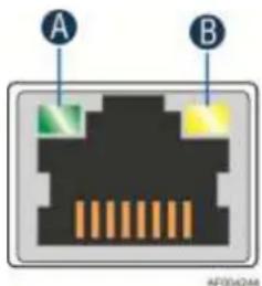
Figure 15. 1GbE NIC Port LED
Table 12. NIC Status LED
| LED Color | LED State | NIC State |
| Green/Amber (B) | Off | 10 Mbps |
| Amber | 100 Mbps | |
| Green | 1000 Mbps | |
| Green (A) | On | Active Connection |
| Blinking | Transmit/Receive activity |
3.4.20.1 MAC Address Definition
The Intel ^® Server Board S2600JF has the following four MAC addresses assigned to it at the Intel factory:
- NIC 1 MAC address (for OS usage)
- NIC 2 MAC address = NIC 1 MAC address + 1 (for OS usage)
■ BMC LAN channel 1 MAC address = NIC1 MAC address + 2 - BMC LAN channel 2 MAC address = NIC1 MAC address + 3
- BMC LAN channel 3 (Dedicated Server Management NIC) MAC address = NIC1 MAC address + 4
The Intel ^® Server Board S2600JF has a white MAC address sticker included with the board. The sticker displays the NIC 1 MAC address in both bar code and alphanumeric formats.
3.4.20.2 LAN Manageability
Port 2 of the Intel ^® i350 NIC is used by the BMC firmware to send management traffic. In standby in order to save power, Port 2 is the only port to support Wake on LAN. The EEPROM is programmed to turn off this feature from the other ports in order to maximize power savings during sleep states.
3.4.20.3 Wake-On-LAN
WOL is supported on the Intel ^® i350 LAN controller for all supported Sleep states.
3.4.20.4 LAN Connector Ordering
The Intel ^® i350 NIC is connected to independent RJ-45 ports for NIC 1 and NIC 2.
3.4.20.5 Thermal Sensor
The Intel ^® i350 NIC has an integrated digital thermal sensor accessible through CSR and manageability registers. The thermal sensor can be programmed to trigger digital pins and thermal throttling with hysteresis.
3.5 InfiniBand\* Controller
Intel ^® Server Board S2600JFQ and JF2600JFF are populated with a new generation InfiniBand ^ adapter device. Mellanox ^ ConnectX-3 ^ supports Virtual Protocol Interconnect ^ (VPI), providing single port 10/20/40/56 Gb/s InfiniBand ^* interfaces. The functional diagram is as follows.
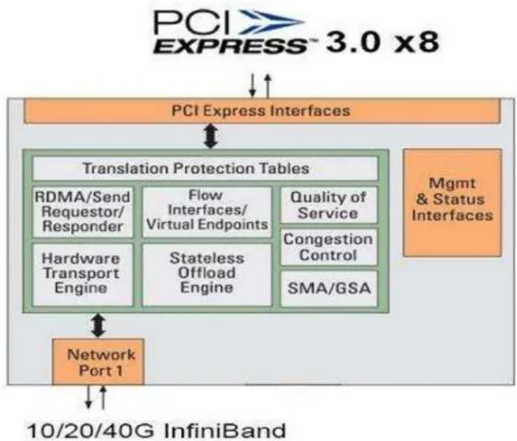
flowchart
graph TD
    A["PCI EXPRESS™ 3.0 x8"] --> B["PCI Express Interfaces"]
    B --> C["Translation Protection Tables"]
    C --> D["RDMA/Send Requestor/Responder"]
    C --> E["Flow Interfaces/Virtual Endpoints"]
    C --> F["Quality of Service"]
    C --> G["Hardware Transport Engine"]
    C --> H["Stateless Offload Engine"]
    C --> I["Congestion Control"]
    C --> J["SMA/GSA"]
    K["Mgmt & Status Interfaces"] --> L["Network Port 1"]
    L --> M["10/20/40G InfiniBand"]
Figure 16. ConnectX ^* -3 Function Block Diagram
Major features and functions include:
- Single InfiniBand* Port: SDR/DDR/QDR/FDR with port remapping in firmware.
■ Performance optimization: Achieving single port line-rate bandwidth. - PCI Express 3.0* x8 to achieve 2.5, 5, or 8GT/s link rate.
- Optimized for LOM: Small footprint, minimal peripherals, WOL, integrated sensors, and BMC interface.
- Low power consumption: 6.5 Watt typical.
3.5.1 Device Interfaces
Following is a list of major interfaces of Mellanox* ConnectX-3* chip:
- Clock and Reset signals: Include core clock input and chip reset signals.
- Uplink Bus: The PCI Express* bus is a high-speed uplink interface used to connect ConnectX-3* to the host processor. The ConnectX-3* supports a PCI Express 3.0* x8 uplink connection with transfer rates of 2.5GT/s, 5GT/s, and 8GT/s per lane.
Throughout this document, the PCI Express* interface may also be referred to as the "uplink" interface. - Network Interface: Single network port connecting the device to a network fabric in one of the configurations described in the following table.
Table 13. Network Port Configuration
| Port Configured as |
| 10/20/40/56 Gb/s InfiniBand* |
- Flash interface: Chip initialization and host boot.
- I ^2 C Compatible Interfaces: For chip, QSFP connector, and chassis configure and monitor.
- Management Link: Connect to BMC through SMBus* and NC-SI.
- Others including: MDIO, GPIO, and JTAG.
3.5.2 Quad Small Form-factor Pluggable (QSFP) Connector
Port of the Mellanox* ConnectX-3* is connected to a single QSFP connector on Intel® Server Board S2600JF (available on SKU: S2600JFQ and S2600JFF). Following is the application reference between Mellanox* ConnectX-3* and QSFP.
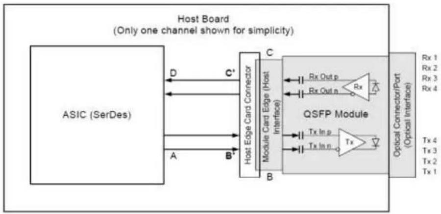
flowchart
graph LR
    A["ASIC (SerDes)"] -->|D| B["Host Edge Card Connector"]
    A -->|A| C["Module Card Edge (Host Interface)"]
    A -->|B+| D["QSFP Module"]
    B -->|Rx Out p| E["Rx"]
    B -->|Rx Out n| F["Rx"]
    C -->|Tx In p| G["Tx"]
    C -->|Tx In n| H["Tx"]
    D --> I["Optical Connector/Port (Optical Interface)"]
    style A fill:#f9f,stroke:#333
    style B fill:#ccf,stroke:#333
    style C fill:#cfc,stroke:#333
    style D fill:#fcc,stroke:#333
    style E fill:#ffc,stroke:#333
    style F fill:#ffc,stroke:#333
    style G fill:#ffc,stroke:#333
    style H fill:#ffc,stroke:#333
    style I fill:#ffc,stroke:#333
Figure 17. Connection between ConnectX -3 and QSFP
The QSFP module and all pins withstand 500V electrostatic discharge based on the Human Body Model per JEDEC JESD22-A114-B.
The module meets ESD requirements given in EN61000-4-2, criterion B test specification so that when installed in a properly grounded cage and chassis the units are subjected to 12KV air discharges during operation and 8KV direct contact discharges to the case.
Note: InfiniBand* cables of 2-meter or 3-meter length are recommended to get better EMI performance.
3.6 Integrated Baseboard Management Controller Overview
The server board utilizes the Baseboard Management features of the ServerEngines* Pilot-III Server Management Controller. The following is an overview of the features implemented on the server board from each embedded controller.
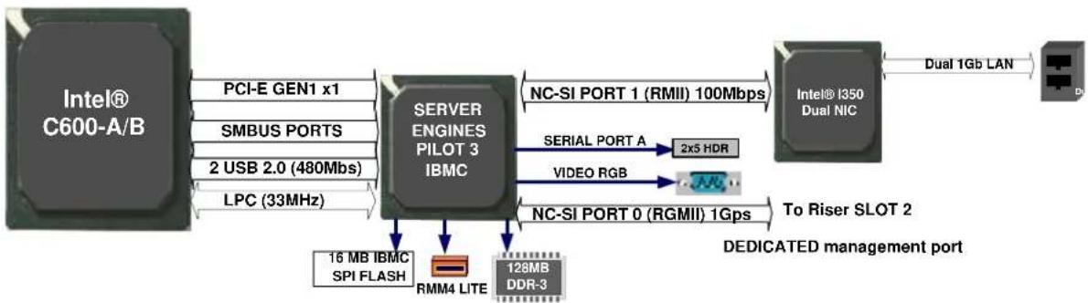
flowchart
graph LR
    A["Intel® C600-A/B"] -->|PCI-E GEN1 x1| B["SERVER ENGINES PILOT 3 IBMC"]
    A -->|SMBUS PORTS| B
    A -->|2 USB 2.0 (480Mbs)| B
    A -->|LPC (33MHz)| B
    B -->|NC-SI PORT 1 (RMII) 100Mbps| C["Intel® I350 Dual NIC"]
    C -->|Dual 1Gb LAN| D["Output"]
    B -->|SERIAL PORT A 2x5 HDR| E["Video RGB"]
    B -->|NC-SI PORT 0 (RGMII) 1Gps| F["To Riser SLOT 2"]
    B --> G["DEDICATED MANAGEMENT PORT"]
    B --> H["16 MB IBMC SPI FLASH"]
    B --> I["RMM4 LITE"]
    B --> J["128MB DDR-3"]
Figure 18. Integrated BMC Implementation Overview
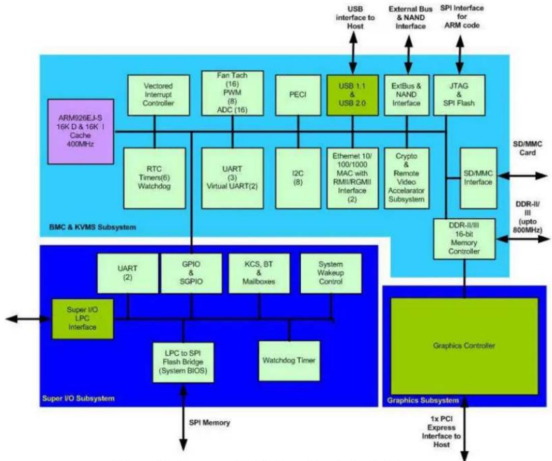
flowchart
graph TD
    A["ARM226EJ-S 16K D & 16K I Cache 400MHz"] --> B["Vectored Interrupt Controller"]
    B --> C["RTC Timers(6) Watchdog"]
    C --> D["UART (3) Virtual UART(2)"]
    D --> E["PAN Tach (16) PWM (8) ADC (16)"]
    E --> F["PECI"]
    F --> G["USB 1.1 & USB 2.0"]
    G --> H["External Bus & NAND Interface"]
    H --> I["ExtBus & NAND Interface"]
    I --> J["JTAG & SPI Flash"]
    J --> K["SD/MMC Interface"]
    K --> L["DDR-II/III 16-bit Memory Controller"]
    L --> M["Graphics Controller"]
    M --> N["1x PCI Express Interface to Host"]
    O["BMC & KVMS Subsystem"] --> P["Super I/O LPC Interface"]
    P --> Q["LPC to SPI Flash Bridge (System BIOS)"]
    Q --> R["Watchdog Timer"]
    R --> S["GPIO & GPIO"]
    S --> T["KCS, BT & Mailboxes"]
    T --> U["System Wakeup Control"]
    U --> V["UART (2)"]
    V --> W["GPIO & GPIO"]
    W --> X["KCS, BT & Mailboxes"]
    X --> Y["System Wakeup Control"]
    Y --> Z["GPS Controller"]
    Z --> AA["Graphics Subsystem"]
    AA --> AB["1x PCI Express Interface to Host"]
    AC["SD/MMC Card"] --> AD["External Bus & NAND Interface"]
    AD --> AE["SPI Interface for ARM code"]
    AF["Super I/O Subsystem"] --> AG["SPi Memory"]
    AG --> AH["Data Flow: USB interface to Host"]
Figure 19. Integrated BMC Functional Block Diagram
The Integrated BMC is provided by an embedded ARM9 controller and associated peripheral functionality that is required for IPMI-based server management. Firmware usage of these hardware features is platform-dependent.
The following is a summary of the Integrated BMC management hardware features that comprise the BMC:
- 400MHz 32-bit ARM9 processor with memory management unit (MMU).
- Two independent10/100/1000 Ethernet Controllers with RMII/RGMII support.
- DDR2/3 16-bit interface with up to 800 MHz operation.
■ 12 10-bit ADCs.
■ 16 fan tachometers. - Eight Pulse Width Modulators (PWM).
- Chassis intrusion logic.
- JTAG Master.
- Eight I ^2 C interfaces with master-slave and SMBus* timeout support. All interfaces are SMBus 2.0* compliant.
-
Parallel general-purpose I/O Ports (16 direct, 32 shared).
-
Serial general-purpose I/O Ports (80 in and 80 out).
- Three UARTs.
■ Platform Environmental Control Interface (PECI).
■ Six general-purpose timers. - Interrupt controller.
■ Multiple SPI flash interfaces.
■ NAND/Memory interface. - 16 mailbox registers for communication between the BMC and host.
- LPC ROM interface.
■ BMC watchdog timer capability.
■ SD/MMC card controller with DMA support. - LED support with programmable blink rate controls on GPIOs.
■ Port 80h snooping capability.
- Secondary Service Processor (SSP), which provides the HW capability of offloading time critical processing tasks from the main ARM core.
Server Engines* Pilot III contains an integrated SIO, KVMS subsystem, and graphics controller with the following features.
3.6.1 Super I/O Controller
The integrated super I/O controller supports the following features implemented on the server board:
- Keyboard Style/BT interface for BMC support
- Two Fully Functional Serial Ports, compatible with the 16C550
- Serial IRQ Support
- Up to 16 Shared GPIO available for host processor
■ Programmable Wake-up Event Support - Plug and Play Register Set
■ Power Supply Control
3.6.1.1 Keyboard and Mouse Support
The server board does not support PS/2 interface keyboards and mice. However, the system BIOS recognizes USB-specification-compliant keyboards and mice.
3.6.1.2 Wake-up Control
The super I/O contains functionality that allows various events to power on and power off the system.
3.6.2 Graphics Controller and Video Support
The integrated graphics controller supports the following features implemented on the server board:
- Integrated Graphics Core with 2D Hardware accelerator
- DDR-2/3 memory interface supports up to 256Mbytes of memory
■ Supports all display resolutions up to 1600 x 1200 16bpp @ 60Hz
■ High speed Integrated 24-bit RAMDAC
The integrated video controller supports all standard IBM VGA modes. The following table shows the 2D modes supported for both CRT and LCD.
Table 14. Supported Video Modes
| 2D Mode | Refresh Rate (Hz) | 2D Video Mode Support | ||
| 8 bpp | 16 bpp | 32 bpp | ||
| 640x480 | 60, 72, 75, 85, 90, 100, 120, 160, 200 | Supported | Supported | Supported |
| 800x600 | 60, 70, 72, 75, 85, 90, 100, 120,160 | Supported | Supported | Supported |
| 1024x768 | 60, 70, 72, 75, 85, 90, 100 | Supported | Supported | Supported |
| 1152x864 | 43, 47, 60, 70, 75, 80, 85 | Supported | Supported | Supported |
| 1280x1024 | 60, 70, 74, 75 | Supported | Supported | Supported |
| 1600x1200** | 60 | Supported | Supported | Supported |
Note:
- Video resolutions at 1600x1200 are only supported through the external video connector located on the rear I/O section of the server board. Utilizing the optional front panel video connector may result in lower video resolutions.
- The server board provides two video interfaces. The primary video interface is accessed using a standard 15-pin VGA connector found on the back edge of the server board. In addition, video signals are routed to a 14-pin header labeled "FP_Video" on the leading edge of the server board, allowing for the option of cabling to a front panel video connector. Attaching a monitor to the front panel video connector disables the primary external video connector on the back edge of the board.
The BIOS supports dual-video mode when an add-in video card is installed.
- In the single mode (dual monitor video = disabled), the on-board video controller is disabled when an add-in video card is detected.
- In the dual mode (on-board video = enabled, dual monitor video = enabled), the on-board video controller is enabled and is the primary video device. The add-in video card is allocated resources and is considered the secondary video device. The BIOS Setup utility provides options to configure the feature as follows.
Table 15. Dual Video Option
| On-board Video | EnabledDisabled | |
| Dual Monitor Video | EnabledDisabled | Shaded if on-board video is set to "Disabled" |
3.6.3 Remote KVM
The Integrated BMC contains a remote KVMS subsystem with the following features:
- USB 2.0 interface for keyboard, mouse, video, and remote storage such as CD/DVD ROM and floppy.
- USB 1.1 / USB 2.0 interface for PS2 to USB bridging, remote keyboard, video, and mouse.
- Hardware Based Video Compression and Redirection Logic.
■ Supports both text and Graphics redirection. - Hardware assisted Video redirection using the Frame Processing Engine.
- Direct interface to the Integrated Graphics Controller registers and Frame buffer.
- Hardware-based encryption engine.
4. Platform Management Functional Overview
Platform management functionality is supported by several hardware and software components integrated on the server board that work together to control system functions, monitor and report system health, and control various thermal and performance features in order to maintain (when possible) server functionality in the event of component failure and/or environmentally stressed conditions.
This chapter provides a high-level overview of the platform management features and functionality implemented on the server board. For more in depth and design level Platform Management information, refer to the BMC Core Firmware External Product Specification (EPS) (Intel Order Number: G31813) and BIOS Core External Product Specification (EPS) for Intel ^® Server products based on the Intel ^® Xeon ^® processor E5-4600, 2600, and 1600 product families.
4.1 Baseboard Management Controller (BMC) Firmware Feature Support
The following sections outline general features that the integrated BMC firmware supports. Support and utilization for some features is dependent on the server platform in which the server board is integrated and any additional system level components and options that may be installed.
4.1.1 IPMI 2.0 Features
- Baseboard management controller (BMC).
■ IPMI Watchdog timer. - Messaging support, including command bridging and user/session support.
- Chassis device functionality, including power/reset control and BIOS boot flags support.
- Event receiver device: The BMC receives and processes events from other platform subsystems.
- Field Replaceable Unit (FRU) inventory device functionality: The BMC supports access to system FRU devices using IPMI FRU commands.
- System Event Log (SEL) device functionality: The BMC supports and provides access to a SEL.
- Sensor Data Record (SDR) repository device functionality: The BMC supports storage and access of system SDRs.
- Sensor device and sensor scanning/monitoring: The BMC provides IPMI management of sensors. It polls sensors to monitor and report system health.
- IPMI interfaces.
- Host interfaces, including system management software (SMS) with receive message queue support, and server management mode (SMM).
- IPMB interfaces.
- LAN interface that supports the IPMI-over-LAN protocol (RMCP and RMCP+).
- Serial-over-LAN (SOL).
- ACPI state synchronization: The BMC tracks ACPI state changes that are provided by the BIOS.
- BMC self-test: The BMC performs initialization and runtime self-tests and makes results available to external entities.
See also the Intelligent Platform Management Interface Specification Second Generation v2.0.
4.1.2 Non-IPMI Features
The BMC supports the following non-IPMI features. This list does not preclude support for future enhancements or additions:
■ In-circuit BMC firmware update.
■ BMC FW reliability enhancements:
- Redundant BMC boot blocks to avoid possibility of a corrupted boot block resulting in a scenario that prevents a user from updating the BMC.
o BMC System Management Health Monitoring. -
Signed firmware images for increased security.
-
Fault resilient booting (FRB): FRB2 is supported by the watchdog timer functionality.
- Enable/Disable of system reset due to CPU errors.
- Chassis intrusion detection.
- Fan speed control.
■ Fan redundancy monitoring and support. - Hot-swap fan support.
■ Power Supply Fan Sensors.
■ System Airflow Monitoring. - Exit Air Temperature Monitoring.
- Acoustic management: Support for multiple fan profiles.
- Ethernet Controller Thermal Monitoring.
- Global Aggregate Temperature Margin Sensor.
- Platform environment control interface (PECI) thermal management support.
■ Memory Thermal Management. - DIMM temperature monitoring: New sensors and improved acoustic management using closed-loop fan control algorithm take into account DIMM temperature readings.
■ Power supply redundancy monitoring and support. - Power unit management: Support for power unit sensor. The BMC handles power-good dropout conditions.
Intel ^® Intelligent Power Node Manager support. - Signal testing support: The BMC provides test commands for setting and getting platform signal states.
- The BMC generates diagnostic beep codes for fault conditions.
■ System GUID storage and retrieval. - Front panel management: The BMC controls the system status LED and chassis ID LED. It supports secure lockout of certain front panel functionality and monitors button presses. The chassis ID LED is turned on using a front panel button or a command.
■ Power state retention.
■ Power fault analysis.
Intel ^® Light-Guided Diagnostics.
- Address Resolution Protocol (ARP): The BMC sends and responds to ARPs (supported on embedded NICs).
- Dynamic Host Configuration Protocol (DHCP): The BMC performs DHCP (supported on embedded NICs).
- Email alerting.
■ Embedded web server.
o Support for embedded web server UI in Basic Manageability feature set.
- Human-readable SEL.
○ Additional system configurability.
○ Additional system monitoring capability.
- Enhanced online help.
- Integrated KVM.
■ Integrated Remote Media Redirection. - Local Directory Access Protocol (LDAP) support.
- Sensor and SEL logging additions/enhancements (for example, additional thermal monitoring capability).
- SEL Severity Tracking and the Extended SEL.
■ BMC Data Repository (Managed Data Region Feature). - Embedded platform debug feature that allows capture of detailed data for later analysis.
-
Provisioning and inventory enhancements:
-
Signed Firmware (improved security).
-
Inventory data/system information export (partial SMBIOS table).
-
DCMI 1.1 compliance.
- Management support for PMBus* rev1.2 compliant power supplies.
■ Energy Star Server Support. - SmaRT/CLST.
■ Power Supply Cold Redundancy.
■ Power Supply FW Update for supported Intel supplies.
■ Power Supply Compatibility Check.
4.1.3 New Manageability Features
The new generation Intel ^® server products offer a number of changes and additions to the manageability features that are supported on the previous generation of servers. The following is a list of the more significant changes that are common to all servers of this new generation:
- Sensor and SEL logging additions/enhancements (for example, additional thermal monitoring capability).
- SEL Severity Tracking and the Extended SEL.
- Embedded platform debug feature that allows capture of detailed data for later analysis.
- Provisioning and inventory enhancements:
- Signed Firmware (improved security).
- Inventory data/system information export (partial SMBIOS table).
■ Enhancements to fan speed control.
- DCMI 1.1 compliance.
- Support for embedded web server UI in basic manageability feature set.
■ Enhancements to embedded web server.
- Human-readable SEL.
○ Additional system configurability.
○ Additional system monitoring capability.
- Enhanced online help.
- Enhancements to KVM redirection.
- Support resolution up to 1600x1200.
- Management support for PMBus* rev1.2 compliant power supplies.
- BMC Data Repository (Managed Data Region Feature).
- System Airflow Monitoring.
- Exit Air Temperature Monitoring.
- Ethernet Controller Thermal Monitoring.
- Global Aggregate Temperature Margin Sensor.
■ Memory Thermal Management.
■ Power Supply Fan Sensors. - Enable/Disable of system reset due to CPU errors.
■ Energy Star Server Support. - SmaRT/CLST.
■ Power Supply Cold Redundancy.
■ Power Supply FW Update.
■ Power Supply Compatibility Check.
■ BMC FW reliability enhancements:
o Redundant BMC boot blocks to avoid possibility of a corrupted boot block resulting in a scenario that prevents a user from updating the BMC.
o BMC System Management Health Monitoring.
4.2 Advanced Configuration and Power Interface (ACPI)
The server board supports the following ACPI states.
Table 16. ACPI Power States
| State | Supported | Description |
| S0 | Yes | Working.The front panel power LED is on (not controlled by the BMC).The fans spin at the normal speed, as determined by sensor inputs.Front panel buttons work normally. |
| S1 | Yes | Sleeping. Hardware context is maintained; equates to processor, and chipset clocks being stopped.The front panel power LED blinks at a rate of 1 Hz with a 50% duty cycle (not controlled by the BMC).The watchdog timer is stopped.The power, reset, front panel NMI, and ID buttons are unprotected.Fan speed control is determined by available SDRs. Fans may be set to a fixed state, or basic fan management can be applied.The BMC detects that the system has exited the ACPI S1 sleep state when the BIOS SMI handler notifies it. |
| S2 | No | Not supported. |
| S3 | No | Supported only on Workstation platforms. See appropriate Platform Specific Information for more information. |
| S4 | No | Not supported. |
| S5 | Yes | Soft off.The front panel buttons are not locked.The fans are stopped.The power-up process goes through the normal boot process.The power, reset, front panel NMI, and ID buttons are unlocked. |
4.3 Platform Management SMBus\* and I ^2 C Implementation
SMBus*/I²C interconnections is a fundamental interface for various manageability components. Three buses are used in a multi-master fashion:
- Primary IPMB. An IPMB header is provided on the baseboard to support connectivity with third-party management PCIe cards. This bus operates as a 100-kHz bus.
- Secondary IPMB. This is the SMLink0 bus that connects the BMC with the ME in the SSB. This bus is considered a secondary IPMB. The ME and BMC communicate over this bus using IPMB protocol messages. Any devices on the bus must be 400-kHz bus tolerant.
- PMBus*. This is the SMLink1 bus that both the ME and BMC use to communicate with the power supplies. This bus operates as a 100-kHz bus.
For all multi-master buses, the master that initiates a transaction is responsible for any bus recovery sequence if the bus hangs.
The BMC acts as a master for the other buses connected to it.
4.4 BMC Internal Timestamp Clock
The BMC maintains an internal timestamp clock that is used by various BMC subsystems, for example, for time stamping SEL entries. As part of BMC initialization after AC power is applied or the BMC is reset, the BMC initializes this internal clock to the value retrieved from the SSB component's RTC through an SMBus* slave read operation. This is the system RTC and is on the battery power well so it maintains the current time even when there is no AC supplied to the system.
The BMC reads the RTC using the same SMBus* (the "host SMBus*") that is used by the BIOS during POST, so the BMC FW must not attempt to access the RTC between the time the system is reset or powered on and POST completes, as indicated by the assertion of the POST-complete signal. Additionally, the BMC should cancel any pending reads of the RTC if the POST-complete signal de-asserts (for example, due to a reset). Normally the BMC reads the RTC when AC power is first applied and before the system is powered on, so this is not a concern. However, if AC power is applied and the power button is immediately pressed, it is possible that POST will be in progress by the time the BMC is ready to read the RTC. Another potential conflict can occur if the BMC gets reset and POST is in progress when the BMC has re-initialized. For either of these cases, the BMC FW initializes its internal time clock to zero and begins counting up from there. When POST completes, the BIOS will then update the BMC's time clock to the current system time.
The BMC's internal timestamp clock is read and set using the Get SEL Time and Set SEL Time commands, respectively. The Get SDR Time command can also be used to read the timestamp clock. These commands and the IPMI time format are specified in the IPMI 2.0 specification. Whenever the BMC receives the Set SEL Time command, it updates only its internal time clock. Note that an update of this internal time clock does not result in a change to the system RTC.
4.5 Sensor Monitoring
The BMC monitors system hardware and reports system health. The information gathered from physical sensors is translated into IPMI sensors as part of the “IPMI Sensor Model”. The BMC also reports various system state changes by maintaining virtual sensors that are not specifically tied to physical hardware.
4.6 Messaging Interfaces
The supported BMC communication interfaces include:
- Host SMS interface by means of low pin count (LPC) / keyboard controller style (KCS) interface
- Host SMM interface by means of low pin count (LPC) / keyboard controller style (KCS) interface
- Intelligent Platform Management Bus (IPMB) I ^2 C interface
■ LAN interface using the IPMI-over-LAN protocols
4.6.1 Channel Management
Every messaging interface is assigned an IPMI channel ID by IPMI 2.0. Commands are provided to configure each channel for privilege levels and access modes. The following table shows the standard channel assignments.
Table 17. Standard Channel Assignments
| Channel ID | Interface | Supports Sessions |
| 0 | Primary IPMB | No |
| 1 | LAN 1 | Yes |
| 2 | LAN 2 | Yes |
| 3 | LAN 3 ^1 (Provided by the Intel ^ Dedicated Server Management NIC) | Yes |
| 4 | Reserved | Yes |
| 5 | USB | No |
| 6 | Secondary IPMB | No |
| 7 | SMM | No |
| 8 – 0Dh | Reserved | - |
| 0Eh | Self ^2 | - |
| 0Fh | SMS/Receive Message Queue | No |
Notes:
- Optional hardware supported by the server system.
- Refers to the actual channel used to send the request.
4.6.2 User Model
The BMC supports the IPMI 2.0 user model including User ID 1 support. Fifteen user IDs are supported. These 15 users can be assigned to any channel. The following restrictions are placed on user-related operations:
- User names for User IDs 1 and 2 cannot be changed. These are always "" (Null/blank) and "root" respectively.
a. A CCh error completion code is returned if a user attempts to modify these names.
- User 2 ("root") always has the administrator privilege level.
a. A CCh error completion code is returned if a user attempts to modify this value. b. Trying to set any parameter for User ID 2 (root user) with the Set User Access command fails with a CCh completion code.
-
All user passwords (including passwords for 1 and 2) may be modified.
-
User IDs 3-15 may be used freely, with the condition that user names are unique. Therefore, no other users can be named "" (Null), "root," or any other existing user name.
Resetting a user name, to a value equivalent to its current value, results in a 0xCC error code. A list of default user values is given in the following table.
Table 18. Default User Values
| Users | User name | Password | Status | Default Privilege | Characteristics |
| User 1 | [Null] | [Null] | Disabled | Admin | Password can be changed.This user may not be used to access the embedded web server. |
| User 2 | root | superuser | Disabled | Admin | Password can be changed. |
| User 3 | test1 | superuser | Disabled | Admin | User name and password can be changed. |
| User 4 | test2 | superuser | Disabled | Admin | User name and password can be changed. |
| User 5 | test3 | superuser | Disabled | Admin | User name and password can be changed. |
| User 6-15 | undefined | undefined | Disabled | Admin | User name and password can be changed. |
4.6.3 Sessions
The maximum number of IPMI-based sessions that can be supported by the BMC is returned as the byte 3 (number of possible active sessions) of the IPMI Command Get Session Info (App, 3Dh). Embedded Web Server and Media Redirection are not IPMI-based sessions. KVM is a type of payload in an RMCP+ Session.
Table 19. Channel/Media-Specific Minimum Number of Sessions
| Channels/Media Type | Session Type | Minimum Number of Sessions |
| LAN Channel1, Intel®Dedicated Server Management NIC4 | IPMI Over LAN1 | 46.7 |
| HTTP5 | Embedded Web Server3 | 28.9 |
| ---5 | Media Redirectionb | 28 |
| ---1 | KVM2 | 210 |
Notes:
- Session type is defined by the IPMI spec and includes RMCP and RMCP+ sessions (including all the payloads supported).
- KVM is an RMCP+ Payload Type, not an IPMI session.
- These sessions are not defined by IPMI Specification and are not based on IPMI protocol. Counting them as IPMI Session violates the Specification.
- If Intel ^ Dedicated Server Management NIC is not present, the minimum number of sessions still holds but only over LAN Channel 1.
- It is not an IPMI Channel.
- Maximum of 15 IPMI sessions are allowed per channel that is defined.
- IPMI-based session is counted as an IPMI Session in all calculations.
- These sessions are not counted as IPMI sessions. (For example, Get Session Info only returns values based on IPMI Sessions.)
- This type of Non-IPMI session can open IPMI sessions as part of a normal operation and those IPMI sessions are counted as IPMI sessions. For example, within a Web Session, one or more IPMI Over LAN Session is opened to Get and Set IPMI parameters. But because these IPMI sessions are not over
LAN1 or Intel ^® Dedicated Server Management NIC, they are not counted as LAN1 or Intel ^® Dedicated Server Management NIC IPMI channel sessions but are counted as IPMI sessions in limit calculations. 10. It is an IPMI Over LAN RMCP+ session and is included in counts as part of the larger IPMI Over LAN group.
Note: The number of possible active session values returned by Get Session Info is the total number of allocated memory session slots in BMC firmware for IPMI Sessions. The actual number of IPMI sessions that can be established at any time is dependent on Channel and User IPMI configuration parameters and in compliance with the IPMI Specification, which is always less than the total available slots.
4.6.4 BMC LAN Channels
The BMC supports three RMII/RGMII ports that can be used for communicating with Ethernet devices. Two ports are used for communication with the on-board NICs and one is used for communication with an Ethernet PHY located on an optional add-in card (or equivalent on-board circuitry).
4.6.4.1 Baseboard NICs
The specific Ethernet controller (NIC) used on a server is platform-specific but all baseboard device options support an NC-SI manageability interface. This provides a sideband high-speed connection for manageability traffic to the BMC while still allowing for a simultaneous host access to the OS if desired.
The Network Controller Sideband Interface (NC-SI) is a DMTF industry standard protocol for the side band management LAN interface. This protocol provides a fast multi-drop interface for traffic management.
The baseboard NICs are connected to a single BMC RMII/RGMII port that is configured for RMII operation. The NC-SI protocol is used for this connection and provides a 100 Mb/s full-duplex multi-drop interface that allows multiple NICs to be connected to the BMC. The physical layer is based upon RMII, however RMII is a point-to-point bus whereas NC-SI allows one master and up to four slaves. The logical layer (Configuration commands) is incompatible with RMII.
Multi-port baseboard NICs on some products support a dedicated management channel that can be configured to be hidden from the host and only used by the BMC. This mode of operation is configured through a BIOS setup option.
4.6.4.2 Dedicated Management Channel
An additional LAN channel dedicated to BMC usage and not available to host SW is supported through an optional add-in card. There is only a PHY device present on the add-in card. The BMC has a built-in MAC module that uses the RGMII interface to link with the card's PHY. Therefore, for this dedicated management interface, the PHY and MAC are located in different devices.
The PHY on the card connects to the BMC's other RMII/RGMII interface (the one that is not connected to the baseboard NICs). This BMC port is configured for RGMII usage.
In addition to the use of an add-in card for a dedicated management channel, on systems that support multiple Ethernet ports on the baseboard, the system BIOS provides a setup option to allow one of these baseboard ports to be dedicated to the BMC for manageability purposes. When this is enabled, that port is hidden from the OS.
4.6.4.3 Concurrent Server Management Use of Multiple Ethernet Controllers
Provided the HW supports a management link between the BMC and a NIC port, the BMC FW supports concurrent OOB LAN management sessions for the following combinations:
■ Two on-board NIC ports
- One on-board NIC and the optional dedicated add-in management NIC
- Two on-board NICs and optional dedicated add-in management NIC
All NIC ports must be on different subnets for the concurrent usage models above.
MAC addresses are assigned for management NICs from a pool of up to three MAC addresses allocated specifically for manageability. The total number of MAC addresses in the pool is dependent on the product HW constraints (for example, a board with two NIC ports available for manageability will have a MAC allocation pool of two addresses).
For these channels, support can be enabled for IPMI-over-LAN and DHCP.
For security reasons, embedded LAN channels have the following default settings:
■ IP Address: Static
- All users disabled
Network failover mode must be used for IPMI-capable interfaces that are on the same subnet.
Host-BMC communication over the same physical LAN connection – also known as “loopback” – is not supported. This includes “ping” operations.
On baseboards with more than two on-board NIC ports, only the first two ports can be used as BMC LAN channels. The remaining ports have no BMC connectivity.
Maximum bandwidth supported by BMC LAN channels are as follows:
■ BMC LAN1 (Baseboard NIC port) 1000M (10M in DC off state)
■ BMC LAN 2 (Baseboard NIC port) 1000M (10M in DC off state)
■ BMC LAN 3 (Dedicated NIC) 1000M
4.6.5 IPv6 Support
In addition to IPv4, the Intel ^® Server Board S2600JF supports IPv6 for manageability channels. Configuration of IPv6 is provided by extensions to the IPMI Set and Get LAN Configuration Parameters commands as well as through a Web Console IPv6 configuration web page.
The BMC supports IPv4 and IPv6 simultaneously so they are both configured separately and completely independently. For example, IPv4 can be DHCP configured while IPv6 is statically configured or vice versa. The parameters for IPv6 are similar to the parameters for IPv4 with the following differences:
- An IPv6 address is 16 bytes vs. 4 bytes for IPv4.
- An IPv6 prefix is 0 to 128 bits whereas IPv4 has a 4-byte subnet mask.
- The IPv6 Enable parameter must be set before any IPv6 packets are sent or received on that channel.
- There are two variants of automatic IP Address Source configuration vs. just DHCP for IPv4.
The three possible IPv6 IP Address Sources for configuring the BMC are:
- Static (Manual): The IP, Prefix, and Gateway parameters are manually configured by the user. The BMC ignores any Router Advertisement messages received over the network.
- DHCPv6: The IP comes from running a DHCPv6 client on the BMC and receiving the IP from a DHCPv6 server somewhere on the network. The Prefix and Gateway are configured by Router Advertisements from the local router. The IP, Prefix, and Gateway are read-only parameters to the BMC user in this mode.
- Stateless auto-configuration: The Prefix and Gateway are configured by the router through Router Advertisements. The BMC derives its IP in two parts: the upper network portion comes from the router and the lower unique portion comes from the BMC's channel MAC address. The 6-byte MAC address is converted into an 8-byte value per the EUI-64* standard. For example, a MAC value of 00:15:17:FE:2F:62 converts into a EUI-64 value of 215:17ff:fefe:2f62. If the BMC receives a Router Advertisement from a router at IP 1:2:3:4::1 with a prefix of 64, it will then generate for itself an IP of 1:2:3:4:215:17ff:fefe:2f62. The IP, Prefix, and Gateway are read-only parameters to the BMC user in this mode.
IPv6 can be used with the BMC's Web Console, JViewer* (remote KVM and Media), and Systems Management Architecture for Server Hardware – Command Line Protocol (SMASH-CLP) interface (ssh). There is no standard yet on how IPMI RMCP or RMCP+ should operate over IPv6 so that is not currently supported.
4.6.5.1 LAN Failover
The BMC FW provides a LAN failover capability so that the failure of the system HW associated with one LAN link will result in traffic being rerouted to an alternate link. This functionality is configurable through IPMI methods as well as through the BMC's Embedded UI, allowing for a user to specify the physical LAN links constitute the redundant network paths or physical LAN links constitute different network paths. The BMC supports an “only-all-or-nothing” approach – that is, all interfaces bonded together, or none are bonded together.
The LAN Failover feature applies only to BMC LAN traffic. It bonds all available Ethernet devices but only one is active at a time. When enabled, if the active connection's leash is lost, one of the secondary connections is automatically configured so that it has the same IP address. Traffic immediately resumes on the new active connection.
The LAN Failover enable/disable command may be sent at any time. After it has been enabled, standard IPMI commands for setting channel configuration that specify a LAN channel other than the first will return an error code.
4.6.6 BMC IP Address Configuration
Enabling the BMC's network interfaces requires using the Set LAN Configuration Parameter command to configure LAN configuration parameter 4, IP Address Source. The BMC supports this parameter as follows:
- 1h, static address (manually configured): Supported on all management NICs. This is the BMC's default value.
- 2h, address obtained by BMC running DHCP: Supported on all management NICs.
IP Address Source value 4h, address obtained by BMC running other address assignment protocol, is not supported on any management NIC.
Attempting to set an unsupported IP address source value has no effect, and the BMC returns error code 0xCC, Invalid data field-in request. Note that values 0h and 3h are no longer supported, and will return a 0xCC error completion code.
4.6.6.1 Static IP Address (IP Address Source Value 0h, 1h, and 3h)
The BMC supports static IP address assignment on all of its management NICs. The IP address source parameter must be set to static before the IP address; the subnet mask or gateway address can be manually set.
The BMC takes no special action when the following IP address source is specified as the IP address source for any management NIC:
- 1h – Static address (manually configured)
The Set LAN Configuration Parameter command must be used to configure LAN configuration parameter 3, IP Address, with an appropriate value.
The BIOS does not monitor the value of this parameter, and it does not execute DHCP for the BMC under any circumstances, regardless of the BMC configuration.
Static LAN Configuration parameters can be configured as followings:
When the IP Address Configuration parameter is set to 01h (static), the following parameters may be changed by the user:
■ LAN configuration parameter 3 (IP Address)
■ LAN configuration parameter 6 (Subnet Mask)
■ LAN configuration parameter 12 (Default Gateway Address)
When changing from DHCP to Static configuration, the initial values of these three parameters will be equivalent to the existing DHCP-set parameters. Additionally, the BMC observes the following network safety precautions:
- The user may only set a subnet mask that is valid, per IPv4 and RFC 950 (Internet Standard Subnetting Procedure). Invalid subnet values return a 0xCC (Invalid Data Field in Request) completion code, and the subnet mask is not set. If no valid mask has been previously set, default subnet mask is 0.0.0.0.
- The user may only set a default gateway address that can potentially exist within the subnet specified above. Default gateway addresses outside the BMC's subnet are technically unreachable and the BMC will not set the default gateway address to an
unreachable value. The BMC returns a 0xCC (Invalid Data Field in Request) completion code for default gateway addresses outside its subnet.
- If a command is issued to set the default gateway IP address before the BMC's IP address and subnet mask are set, the default gateway IP address is not updated and the BMC returns 0xCC.
If the BMC's IP address on a LAN channel changes while a LAN session is in progress over that channel, the BMC does not take action to close the session except through a normal session timeout. The remote client must re-sync with the new IP address. The BMC's new IP address is only available in-band through the Get LAN Configuration Parameters command.
4.6.6.2 Enabling/Disableing Dynamic Host Configuration Protocol (DHCP)
The BMC DHCP feature is activated by using the Set LAN Configuration Parameter command to set LAN configuration parameter 4, IP Address Source, to 2h: "address obtained by BMC running DHCP". Once this parameter is set, the BMC initiates the DHCP process within approximately 100 ms.
If the BMC has previously been assigned an IP address through DHCP or the Set LAN Configuration Parameter command, it requests that same IP address to be reassigned. If the BMC does not receive the same IP address, system management software must be reconfigured to use the new IP address. The new address is only available in-band, through the IPMI Get LAN Configuration Parameters command.
Changing the IP Address Source parameter from 2h to any other supported value will cause the BMC to stop the DHCP process. The BMC uses the most recently obtained IP address until it is reconfigured.
If the physical LAN connection is lost (that is, the cable is unplugged), the BMC will not re-initiate the DHCP process when the connection is re-established.
Users may not change the following LAN parameters while the DHCP is enabled:
■ LAN configuration parameter 3 (IP Address)
■ LAN configuration parameter 6 (Subnet Mask)
■ LAN configuration parameter 12 (Default Gateway Address)
To prevent users from disrupting the BMC's LAN configuration, the BMC treats these parameters as read-only while DHCP is enabled for the associated LAN channel. Using the Set LAN Configuration Parameter command to attempt to change one of these parameters under such circumstances has no effect, and the BMC returns error code 0xD5, "Cannot Execute Command. Command, or request parameter(s) are not supported in present state."
4.6.7 DHCP BMC Hostname
The BMC allows setting a DHCP Hostname. DHCP Hostname can be set regardless of the IP Address source configured on the BMC. But this parameter is only used if the IP Address source is set to DHCP.
4.6.8 Address Resolution Protocol (ARP)
The BMC can receive and respond to ARP requests on BMC NICs. Gratuitous ARPs are supported, and disabled by default.
4.6.9 Virtual Local Area Network (VLAN)
The BMC supports VLAN as defined by IPMI 2.0 specifications. VLAN is supported internally by the BMC, not through switches. VLAN provides a way of grouping a set of systems together so that they form a logical network. This feature can be used to set up a management VLAN where only devices that are members of the VLAN will receive packets related to management and members of the VLAN will be isolated from any other network traffic. Note that VLAN does not change the behavior of the host network setting; it only affects the BMC LAN communication.
LAN configuration options are now supported (by means of the Set LAN Config Parameters command, parameters 20 and 21) that allow support for 802.1Q VLAN (Layer 2). This allows VLAN headers/packets to be used for IPMI LAN sessions. VLAN IDs are entered and enabled by means of parameter 20 of the Set LAN Config Parameters IPMI command. When a VLAN ID is configured and enabled, the BMC only accepts packets with that VLAN tag/ID. Conversely, all BMC generated LAN packets on the channel include the given VLAN tag/ID. Valid VLAN IDs are 1 through 4094, with 0 and 4095 reserved, per the 802.1Q VLAN specification. Only one VLAN can be enabled at any point in time on a LAN channel. If an existing VLAN is enabled, it must first be disabled prior to configuring a new VLAN on the same LAN channel.
Parameter 21 (VLAN Priority) of the Set LAN Config Parameters IPMI command is now implemented and a range from 0-7 will be allowed for VLAN Priorities. Note that bits 3 and 4 of Parameter 21 are considered Reserved bits.
Parameter 25 (VLAN Destination Address) of the Set LAN Config Parameters IPMI command is not supported and returns a completion code of 0x80 (parameter not supported) for any read/write of parameter 25.
If the BMC IP address source is DHCP, the following behavior is seen:
- If the BMC is first configured for DHCP (prior to enabling VLAN), when VLAN is enabled, the BMC performs a discovery on the new VLAN in order to obtain a new BMC IP address.
- If the BMC is configured for DHCP (before disabling VLAN), when VLAN is disabled, the BMC performs a discovery on the LAN in order to obtain a new BMC IP address.
If the BMC IP address source is Static, the following behavior is seen:
- If the BMC is first configured for static (prior to enabling VLAN), when VLAN is enabled, the BMC has the same IP address that was configured before. It is left to the management application to configure a different IP address if that is not suitable for VLAN.
- If the BMC is configure for static (prior to disabling VLAN), when VLAN is disabled, the BMC has the same IP address that was configured before. It is left to the management application to configure a different IP address if that is not suitable for LAN.
4.6.10 Secure Shell (SSH)
Secure Shell (SSH) connections are supported for one SMASH-CLP session to the BMC.
4.6.11 Serial-over-LAN (SOL 2.0)
The BMC supports IPMI 2.0 SOL.
IPMI 2.0 introduced a standard serial-over-LAN feature. This is implemented as a standard payload type (01h) over RMCP+.
Three commands are implemented for SOL 2.0 configuration.
- Get SOL 2.0 Configuration Parameters and Set SOL 2.0 Configuration Parameters: These commands are used to get and set the values of the SOL configuration parameters. The parameters are implemented on a per-channel basis.
- Activating SOL: This command is not accepted by the BMC. It is sent by the BMC when SOL is activated to notify a remote client of the switch to SOL.
- Activating a SOL session requires an existing IPMI-over-LAN session. If encryption is used, it should be negotiated when the IPMI-over LAN session is established. SOL sessions are only supported on serial port 1 (COM1).
4.6.12 Platform Event Filter (PEF)
The BMC includes the ability to generate a selectable action, such as a system power-off or reset, when a match occurs to one of a configurable set of events. This capability is called Platform Event Filtering, or PEF. One of the available PEF actions is to trigger the BMC to send a LAN alert to one or more destinations.
The BMC supports 20 PEF filters. The first 12 entries in the PEF filter table are pre-configured (but may be changed by the user). The remaining entries are left blank, and may be configured by the user.
Table 20. Factory Configured PEF Table Entries
| Event Filter Number | Offset Mask | Events |
| 1 | Non-critical, critical and non-recoverable | Temperature sensor out of range |
| 2 | Non-critical, critical and non-recoverable | Voltage sensor out of range |
| 3 | Non-critical, critical and non-recoverable | Fan failure |
| 4 | General chassis intrusion | Chassis intrusion (security violation) |
| 5 | Failure and predictive failure | Power supply failure |
| 6 | Uncorrectable ECC | BIOS |
| 7 | POST error | BIOS: POST code error |
| 8 | FRB2 | Watchdog Timer expiration for FRB2 |
| 9 | Policy Correction Time | Node Manager |
| 10 | Power down, power cycle, and reset | Watchdog timer |
| 11 | OEM system boot event | System restart (reboot) |
| 12 | Drive Failure, Predicted Failure | Hot Swap Controller |
Additionally, the BMC supports the following PEF actions:
■ Power off
■ Power cycle
- Reset
- OEM action
- Alerts
The "Diagnostic interrupt" action is not supported.
4.6.13 LAN Alerting
The BMC supports sending embedded LAN alerts, called SNMP PET (Platform Event traps), and SMTP email alerts.
The BMC supports a minimum of four LAN alert destinations.
4.6.14 SNMP Platform Event Traps (PETs)
This feature enables a target system to send SNMP traps to a designated IP address by means of LAN. These alerts are formatted per the Intelligent Platform Management Interface Specification Second Generation v2.0. A MIB file associated with the traps is provided with the BMC firmware to facilitate interpretation of the traps by external software.
The format of the MIB file is covered under RFC 2578.
4.6.15 Alert Policy Table
Associated with each PEF entry is an alert policy that determines which IPMI channel the alert is to be sent. There is a maximum of 20 alert policy entries. There are no pre-configured entries in the alert policy table because the destination types and alerts may vary by user. Each entry in the alert policy table contains four bytes for a maximum table size of 80 bytes.
4.6.16 Email Alerting
The Embedded Email Alerting feature allows the user to receive email alerts indicating issues with the server. This allows email alerting in an OS-absent (for example, Pre-OS and OS-Hung) situation. This feature provides support for sending email by means of SMTP, the Simple Mail Transport Protocol as defined in Internet RC 821. The email alert provides a text string that describes a simple description of the event. SMTP alerting is configured using the embedded web server.
4.6.17 SM-CLP (SM-CLP Lite)
SMASH refers to Systems Management Architecture for Server Hardware. SMASH is defined by a suite of specifications, managed by the DMTF, that standardize the manageability interfaces for server hardware. CLP refers to Command Line Protocol. SM-CLP is defined by the Server Management Command Line Protocol Specification (SM-CLP) ver1.0, which is part of the SMASH suite of specifications. The specifications and further information on SMASH can be found at the DMTF website (http://www.dmtf.org/).
The BMC provides an embedded “lite” version of SM-CLP that is syntax-compatible but not considered fully compliant with the DMTF standards.
4.7 System Event Log (SEL)
The BMC implements the system event log as specified in the Intelligent Platform Management Interface Specification, Version 2.0. The SEL is accessible regardless of the system power state through the BMC's in-band and out-of-band interfaces.
The BMC allocates 65,502 bytes (approx. 64 KB) of non-volatile storage space to store system events. The SEL timestamps may not be in order. Up to 3,639 SEL records can be stored at a time. Any command that results in an overflow of the SEL beyond the allocated space is rejected with an “Out of Space” IPMI completion code (C4h).
4.7.1 Servicing Events
Events can be received while the SEL is being cleared. The BMC implements an event message queue to avoid the loss of messages. Up to three messages can be queued before messages are overwritten.
The BMC recognizes duplicate event messages by comparing sequence numbers and the message source. For details, see the Intelligent Platform Management Interface Specification Second Generation v2.0. Duplicate event messages are discarded (filtered) by the BMC after they are read from the event message queue. The queue can contain duplicate messages.
4.7.2 SEL Entry Deletion
The BMC does not support individual SEL entry deletion. The SEL may only be cleared as a whole.
4.7.3 SEL Erasure
SEL erasure is a background process. After initiating erasure with the Clear SEL command, additional Clear SEL commands must be executed to get the erasure status and determine when the SEL erasure is completed. This may take several seconds. SEL events that arrive during the erasure process are queued until the erasure is complete and then committed to the SEL.
SEL erasure generates an Event Logging Disabled (Log Area Reset/Cleared offset) sensor event.
4.7.4 SEL Extension Capabilities
The BMC provides an OEM extension to all SEL entries. Each entry includes an additional eight bytes for storing extra event data that will not fit into the original three data bytes provided by standard IPMI SEL entries. The first extension byte is always valid for all SEL entries and specifies the severity of the SEL event as well as the number of valid extension bytes following the first one. That leaves up to seven SEL extension data bytes that can be defined for each SEL event entry.
All standard IPMI SEL commands work the same as if there were no SEL extensions.
In order to store and access the extended SEL information, five OEM commands are implemented that closely follow the standard IPMI SEL commands but provide support for the SEL Extension data. These OEM commands are specified in the Intel ^® General Application Commands table.
4.8 Sensor Data Record (SDR) Repository
The BMC implements the sensor data record (SDR) repository as specified in the Intelligent Platform Management Interface Specification, Version 2.0. The SDR is accessible through the BMC's in-band and out-of-band interfaces regardless of the system power state. The BMC allocates 65,519 bytes of non-volatile storage space for the SDR.
4.9 Field Replaceable Unit (FRU) Inventory Device
The BMC implements the interface for logical FRU inventory devices as specified in the Intelligent Platform Management Interface Specification, Version 2.0. This functionality provides commands used for accessing and managing the FRU inventory information. These commands can be delivered through all interfaces.
The BMC provides FRU device command access to its own FRU device and to the FRU devices throughout the server. The FRU device ID mapping is defined in the Platform Specific Information. The BMC controls the mapping of the FRU device ID to the physical device.
4.10 Diagnostics and Beep Code Generation
The BMC may generate beep codes upon detection of failure conditions. Beep codes are sounded each time the problem is discovered (for example, on each power-up attempt), but are not sounded continuously. Common supported codes are listed in Table 21.
Additional platform-specific beep codes can be found in the appropriate Platform Specific Information. Each digit in the code is represented by a sequence of beeps whose count is equal to the digit.
Table 21. BMC Beep Codes
| Code | Reason for Beep | Associated Sensors | Supported |
| 1-5-2-1 | No CPUs installed or first CPU socket is empty. | CPU Missing Sensor | Yes |
| 1-5-2-4 | MSID Mismatch. | MSID Mismatch Sensor | Yes |
| 1-5-4-2 | Power fault: DC power is unexpectedly lost (power good dropout). | Power unit – power unit failure offset | Yes |
| 1-5-4-4 | Power control fault (power good assertion timeout). | Power unit – soft power control failure offset | Yes |
| 1-5-1-2 | VR Watchdog Timer sensor assertion. | VR Watchdog Timer | Yes |
| 1-5-1-4 | The system does not power on or unexpectedly powers off and a power supply unit (PSU) is present that is an incompatible model with one or more other PSUs in the system. | PSU status | Yes |
4.11 Diagnostics Interrupt (NMI)
The BMC generates an NMI pulse under certain conditions. The BMC-generated NMI pulse duration is at least 30ms. After an NMI has been generated by the BMC, the BMC does not generate another NMI until the system has been reset or powered down.
The following actions cause the BMC to generate an NMI pulse:
a. Receiving a Chassis Control command to pulse the diagnostic interrupt. This command does not cause an event to be logged in the SEL.
b. Detecting that the front panel diagnostic interrupt button has been pressed.
c. Watchdog timer pre-timeout expiration with NMI/diagnostic interrupt pre-timeout action enabled.
The following table shows behavior regarding NMI signal generation and event logging by the BMC.
Table 22. NMI Signal Generation and Event Logging
| Causal Event | NMI (IA-32 Only) | |
| Signal Generation | Front Panel Diag Interrupt Sensor Event Logging Support | |
| Chassis Control command (pulse diagnostic interrupt) | X | - |
| Front panel diagnostic interrupt button pressed | X | X |
| Watchdog Timer pre-timeout expiration with NMI/diagnostic interrupt action | X | - |
4.12 BMC Basic and Advanced Management Features
The Intel ^® Server Board S2600JF product provides an upgrade module to support the advanced server management functionality.
Table 23. Basic and Advanced Management Features
| Feature | Basic* | Advanced** |
| IPMI 2.0 Feature Support | X | X |
| In-circuit BMC Firmware Update | X | X |
| FRB 2 | X | X |
| Chassis Intrusion Detection | X | X |
| Fan Redundancy Monitoring | X | X |
| Hot-Swap Fan Support | X | X |
| Acoustic Management | X | X |
| Diagnostic Beep Code Support | X | X |
| Power State Retention | X | X |
| ARP/DHCP Support | X | X |
| PECI Thermal Management Support | X | X |
| Email Alerting | X | X |
| Embedded Web Server | X | X |
| SSH Support | X | X |
| Integrated KVM | X | |
| Integrated Remote Media Redirection | X | |
| Local Directory Access Protocol (LDAP) | X | X |
| Intel® Intelligent Power Node Manager Support*** | X | X |
| SMASH CLP | X | X |
* Basic management features provided by Integrated BMC.
**Advanced management features available with optional Intel® Remote Management Module 4 Lite.
***Intel ^® Intelligent Power Node Manager Support requires PMBus*-compliant power supply.
4.12.1 Enabling Advanced Manageability Features
The Advanced management features are to be delivered as part of the BMC FW image. The BMC's baseboard SPI flash contains code/data for both the Basic and Advanced features. An optional module Intel® RMM4 Lite is used as the activation mechanism. When the BMC FW initializes, it attempts to access the Intel® RMM4 lite. If the attempt to access Intel® RMM4 Lite is successful, the BMC activates the advanced features.
Advanced manageability features are supported over all NIC ports enabled for server manageability. This includes baseboard NICs as well as the LAN channel provided by the optional Dedicated NIC add-in card.
Table 24. Management Features and Benefits
| Manageability Hardware | Benefits |
| Intel® Integrated BMC | Comprehensive IPMI based base manageability features |
| Intel® Remote Management Module4 – Lite Package contains one module:▪ Key for advance Manageability features. | No dedicated NIC for managementEnables KVM and media redirection through on-board NIC |
| Intel® Remote Management4 ModulePackage includes 2 modules:▪ Key for advance features▪ Dedicated NIC (1Gbe) for management | Dedicated NIC for management traffic. Higher bandwidth connectivity for KVM and media Redirection with 1Gbe NIC. |
4.12.1.1 Keyboard, Video, and Mouse (KVM) Redirection
The BMC firmware supports keyboard, video, and mouse redirection (KVM) over LAN. This feature is available remotely from the embedded web server as a Java* applet. This feature is enabled when the Intel® RMM4 Lite is present. The client system must have a Java* Runtime Environment (JRE) version 5.0 or later to run the KVM or media redirection applets.
The Integrated BMC supports an embedded KVM application (Remote Console) that can be launched from the embedded web server from a remote console. USB1.1 or USB 2.0 based mouse and keyboard redirection is supported. It is also possible to use the KVM-redirection (KVM-r) session concurrently with media-redirection (media-r). This feature allows a user to interactively use the keyboard, video, and mouse (KVM) functions of the remote server as if the user were physically at the managed server.
The KVM- redirection feature automatically senses video resolution for best possible screen capture and provides high-performance mouse tracking and synchronization. It allows remote viewing and configuration in pre-boot POST and BIOS setup, after BIOS has initialized video.
Other attributes of this feature include:
- Encryption of the redirected screen, keyboard, and mouse
■ Compression of the redirected screen
4.12.1.2 Remote Console
The Remote Console is the redirected screen, keyboard, and mouse of the remote host system. To use the Remote Console window of your managed host system, the browser must include a Java* Runtime Environment plug-in. If the browser has no Java* support, such as with a small handheld device, the user can maintain the remote host system using the administration forms displayed by the browser.
The Remote Console window is a Java* Applet that establishes TCP connections to the Integrated BMC. The protocol that is run over these connections is a unique KVM protocol and not HTTP or HTTPS. This protocol uses ports #7578 for KVM, #5120 for CDROM media redirection, and #5123 for Floppy/USB media redirection (both supporting encryption).
4.12.1.3 Performance
The remote display accurately represents the local display. The feature adapts to changes to the video resolution of the local display and continues to work smoothly when the system transitions from graphics to text or vice versa. The responsiveness may be slightly delayed depending on the bandwidth and latency of the network.
Enabling KVM and/or media encryption degrades performance. Enabling video compression provides the fastest response while disabling compression provides better video quality.
For the best possible KVM performance, a 2Mb/sec link or higher is recommended.
The redirection of KVM over IP is performed in parallel with the local KVM without affecting the local KVM operation.
4.12.1.4 Security
The KVM redirection feature supports multiple encryption algorithms, including RC4 and AES. The actual algorithm that is used is negotiated with the client based on the client's capabilities.
4.12.1.5 Availability
The remote KVM session is available even when the server is powered off (in standby mode). No restart of the remote KVM session is required during a server reset or power on/off. An Integrated BMC reset (for example, due to an Integrated BMC Watchdog initiated reset or Integrated BMC reset after Integrated BMC firmware update) requires the session to be re-established.
KVM sessions persist across system reset, but not across an AC power loss.
4.12.1.6 Timeout
The remote KVM session will automatically timeout after a configurable amount of time (30 minutes by default).
The default inactivity timeout is 30 minutes, but may be changed through the embedded web server. Remote KVM activation does not disable the local system keyboard, video, or mouse. Remote KVM is not deactivated by local system input, unless the feature is disabled locally.
4.12.1.7 Usage
When the server is powered up, the remote KVM session displays the complete BIOS boot process. The user can interact with BIOS setup, change and save settings as well as enter and interact with option ROM configuration screens.
At least two concurrent remote KVM sessions are supported. It is possible for at least two different users to connect to the same server and start remote KVM sessions.
4.12.2 Media Redirection
The embedded web server provides a Java* applet to enable remote media redirection. This may be used in conjunction with the remote KVM feature, or as a standalone applet.
The media redirection feature is intended to allow system administrators or users to mount a remote USB HDD or USB CD-ROM, floppy drive, or a USB flash disk as a remote device to the server. After mounted, the remote device appears just like a local device to the server, allowing system administrators or users to install software (including operating systems), copy files, update BIOS, and so on, or boot the server from this device.
The following capabilities are supported:
- The operation of remotely mounted devices is independent of the local devices on the server. Both remote and local devices are usable in parallel.
- It is possible to boot all supported operating systems from the remotely mounted device and to boot from disk IMAGE (*.IMG) and CD-ROM or DVD-ROM ISO files. See the Tested/supported Operating System List for more information.
- Media redirection supports redirection for a minimum of two virtual devices concurrently with any combination of devices. As an example, a user can redirect two CD or two USB devices.
- The media redirection feature supports multiple encryption algorithms, including RC4 and AES. The actual algorithm that is used is negotiated with the client based on the client's capabilities.
- A remote media session is maintained even when the server is powered off (in standby mode). No restart of the remote media session is required during a server reset or power on/off. An Integrated BMC reset (for example, due to an Integrated BMC reset after Integrated BMC firmware update) requires the session to be re-established.
- The mounted device is visible to (and usable by) managed system's OS and BIOS in both pre-boot and post-boot states.
- The mounted device shows up in the BIOS boot order and it is possible to change the BIOS boot order to boot from this remote device.
- It is possible to install an operating system on a bare metal server (no OS present) using the remotely mounted device. This may also require the use of KVM-r to configure the OS during installation.
- USB storage devices appear as floppy disks over media redirection. This allows for the installation of device drivers during OS installation.
- If either a virtual floppy device is remotely attached during system boot, the virtual floppy is presented as a bootable device. It is not possible to present only a single-mounted device type to the system BIOS.
Note: When trying to attach a local floppy or local USB key drive, if it is in use by the operating system or any other application it will fail to attach.
With Microsoft Windows 2008 ^ , Microsoft Windows 2008 ^ R2, and Microsoft Windows 7 ^* , if a Windows Explorer GUI is opened after the USB Key has been installed in the local system, you may not be able to attach the USB Key as remote media.
With Microsoft Windows 2003* and Microsoft Windows XP*, if a Windows Explorer GUI is opened after the USB Key has been installed in the local system and you then browse through the USB Key, you may not be able to attach the USB Key as remote media.
4.12.2.1 Availability
The default inactivity timeout is 30 minutes and is not user-configurable.
Media redirection sessions persist across system reset but not across an AC power loss or BMC reset.
4.12.2.2 Network Port Usage
The KVM and media redirection features use the following ports:
■ 5120 – CD Redirection
■ 5123 – FD Redirection
■ 5124 – CD Redirection (Secure)
■ 5127 – FD Redirection (Secure)
■ 7578 – Video Redirection
■ 7582 – Video Redirection (Secure)
4.12.3 Embedded Web Server
Integrated BMC Base manageability provides an embedded web server and an OEM-customizable web GUI that exposes the manageability features of the Integrated BMC base feature set. It is supported over all on-board NICs that have management connectivity to the Integrated BMC as well as an optional dedicated add-in management NIC. At least two concurrent web sessions from up to two different users are supported. The embedded web user interface supports the following client web browsers:
■ Microsoft Internet Explorer 7.0*
■ Microsoft Internet Explorer 8.0*
■ Microsoft Internet Explorer 9.0*
- Mozilla Firefox* 3.0
- Mozilla Firefox* 3.5
- Mozilla Firefox* 3.6
The embedded web user interface supports strong security (authentication, encryption, and firewall support) because it enables remote server configuration and control. The user interface presented by the embedded web user interface authenticates the user before allowing a web session to be initiated. Encryption using 128-bit SSL is supported. User authentication is based on user id and password.
The GUI presented by the embedded web server authenticates the user before allowing a web session to be initiated. It presents all functions to all users but grays out those functions that the user does not have privilege to execute. (For example, if a user does not have privilege to power control, the item will be displayed in gray-out font in that user's UI display). The web GUI also provides a launch point for some of the advanced features, such as KVM and media redirection. These features are grayed out in the GUI unless the system has been updated to support these advanced features.
A partial list of additional features supported by the web GUI includes:
■ Present all the Basic features to the users.
- Power on/off/reset the server and view current power state.
■ Virtual front panel display and overall system health.
- Provide embedded firmware version information.
- Configuration of various IPMI parameters (LAN parameters, users, passwords, and so on.)
- Configuration of alerting (SNMP and SMTP).
- Display system asset information for the product, board, and chassis.
- Display of BMC-owned sensors (name, status, current reading, and enabled thresholds), including color-code status of sensors.
- Automatic refresh of sensor data with a configurable refresh rate.
- Online help.
- Display/clear SEL (display is in easily understandable human readable format).
■ Support major industry-standard browsers (Internet Explorer* and Mozilla Firefox*).
- Automatically log out after user-configurable inactivity period.
- The GUI session automatically times out after a user-configurable inactivity period. By default, this inactivity period is 30 minutes.
- Embedded Platform Debug feature – Allow the user to initiate a “diagnostic dump” to a file that can be sent to Intel for debug purposes.
- Display of power statistics (current, average, minimum, and maximum) consumed by the server.
4.12.4 Data Center Management Interface (DCMI)
The DCMI Specification is an emerging standard that is targeted to provide a simplified management interface for Internet Portal Data Center (IPDC) customers. It is expected to become a requirement for server platforms that are targeted for IPDCs. DCMI is an IPMI-based standard that builds upon a set of required IPMI standard commands by adding a set of DCMI-specific IPMI OEM commands. The S2600CP platforms implement the mandatory DCMI features in the BMC FW (DCMI 1.1 Errata 1 compliance).
4.12.5 Local Directory Authentication Protocol (LDAP)
The Lightweight Directory Access Protocol (LDAP) is an application protocol supported by the Integrated BMC for the purpose of authentication and authorization. The Integrated BMC user connects with an LDAP server for login authentication. This is only supported for non-IPMI logins including the embedded web UI and SM-CLP. IPMI users/passwords and sessions are not supported over LDAP.
LDAP can be configured (IP address of LDAP server, port, and so on.) through the Integrated BMC's Embedded Web UI. LDAP authentication and authorization is supported over the any NIC configured for system management. The BMC uses a standard Open LDAP implementation for Linux*.
4.12.6 Platform/Chassis Management
Within an IPMI 2.0 framework, the BMC Firmware provides functionality to support management and control of several aspects of the platform operation. This includes:
- Front Panel Support (for example, secure lockout of power and reset buttons and System Status LED control).
- Hardware/Sensor Monitoring (for example, system voltages, thermal sensors, fans, power supplies, and so on).
- Power/Reset Control and Monitoring (for example, local and remote power/reset control and power restore policy).
- Hardware and Manufacturing Test Features.
- Asset Inventory and System Identification (for example, system GUID and FRU management).
- Thermal and Acoustics Management – The BMC firmware provides a comprehensive set of fan control capabilities utilizing various system thermal sensors (for example, CPU, DIMMs, front panel thermal sensor). Additionally, the BMC participates in the memory CLTT by pushing dim thermal data to the iMC in the CPU.
- Power Management (Node Manager) Support – The BMC firmware provides an external (LAN) interface for a remote management console to communicate with the ME's Node Manager Functionality.
4.12.7 Thermal Control
The system supports thermal management through open loop throttling (OLTT) or static closed loop throttling (CLTT) of system memory based on availability of valid temperature sensors on the installed memory DIMMs. The Integrated Memory Controller (IMC) dynamically changes throttling levels to cap throttling based on memory and system thermal conditions as determined by the system and DIMM power and thermal parameters. There is no support for CLTT on mixed-mode DIMM populations (that is, some installed DIMMs have valid temp sensors and some do not). The Integrated BMC fan speed control functionality is related to the memory throttling mechanism used.
The following terminology is used for the various memory throttling options:
- Static Open Loop Thermal Throttling (Static-OLTT): OLTT control registers are configured by BIOS MRC remain fixed after POST. The system does not change any of the throttling control registers in the embedded memory controller during runtime.
- Static Closed Loop Thermal Throttling (Static-CLTT): CLTT control registers are configured by BIOS MRC during POST. The memory throttling is run as a closed-loop system with the DIMM temperature sensors as the control input. Otherwise, the system does not change any of the throttling control registers in the embedded memory controller during runtime.
- Dynamic Open Loop Thermal Throttling (Dynamic-OLTT): OLTT control registers are configured by BIOS MRC during POST. Adjustments are made to the throttling during runtime based on changes in system cooling (fan speed).
- Dynamic Closed Loop Thermal Throttling (Dynamic-CLTT): CLTT control registers are configured by BIOS MRC during POST. The memory throttling is run as a closed-loop system with the DIMM temperature sensors as the control input. Adjustments are made to the throttling during runtime based on changes in system cooling (fan speed).
4.12.7.1 Fan Speed Control Profiles
BIOS and BMC software work cooperatively to implement system thermal management support. During normal system operation, the BMC retrieves information from the BIOS and monitors several platform thermal sensors to determine the required fan speeds.
In order to provide the proper fan speed control for a given system configuration, the BMC must have the appropriate platform data programmed. Platform configuration data is programmed using the FRUSDR utility during the system integration process and by System BIOS during runtime.
Table 25. Fan Profile Mapping
| Type | Profile | Details |
| OLTT | 0 | Acoustic, 300M altitude |
| OLTT | 1 | Performance, 300M altitude |
| OLTT | 2 | Acoustic, 900M altitude |
| OLTT | 3 | Performance, 900M altitude |
| OLTT | 4 | Acoustic, 1500M altitude |
| OLTT | 5 | Performance, 1500M altitude |
| OLTT | 6 | Acoustic, 3000M altitude |
| OLTT | 7 | Performance, 3000M altitude |
| CLTT | 0 | 300M altitude |
| CLTT | 2 | 900M altitude |
| CLTT | 4 | 1500M altitude |
| CLTT | 6 | 3000M altitude |
4.12.7.2 System Configuration Using FRUSDR Utility
The Field Replaceable Unit and Sensor Data Record Update Utility (FRUSDR utility) is a program used to write platform-specific configuration data to NVRAM on the server board. It allows the user to select which supported chassis (Intel or Non-Intel) and platform chassis configuration is used. Based on the input provided, the FRUSDR writes sensor data specific to the configuration to NVRAM for the BMC controller to read each time the system is powered on.
4.12.8 Node Power On/Off Control
The BMC on each node monitors its fans and temperature for a critical failure. When a critical failure occurs, the node will be powered down by the BMC. When this occurs, the node needs to be manually powered on.
4.13 Intel® Intelligent Power Node Manager
4.13.1 Overview
Power management deals with requirements to manage processor power consumption and manage power at the platform level to meet critical business needs. Node Manager (NM) is a platform-resident technology that enforces power capping and thermal-triggered power capping policies for the platform. These policies are applied by exploiting subsystem knobs (such as processor P and T states) that can be used to control power consumption. NM enables data center power management by exposing an external interface to management software through which platform policies can be specified. It also implements specific data center power management usage models such as power limiting and thermal monitoring.
Note: Support for NM is product-specific. This section details how NM is supported on products that provide this capability.
The NM feature is implemented by a complementary architecture utilizing the ME, BMC, BIOS, and an ACPI-compliant OS. The ME provides the NM policy engine and power control/limiting functions (referred to as Node Manager or NM) while the BMC provides the external LAN link by which external management software can interact with the feature. The BIOS provides system power information utilized by the NM algorithms and also exports ASL code used by OSPM for negotiating processor P and T state changes for power limiting. PMBus*-compliant power supplies provide the capability to monitor input power consumption, which is necessary to support NM.
The NM architecture applicable to this generation of servers is defined by the NPTM Architecture Specification v2.0. NPTM is an evolving technology that is expected to continue to add new capabilities that will be defined in subsequent versions of the specification. The ME NM implements the NPTM policy engine and control/monitoring algorithms defined in the NPTM specification.
4.13.2 Features
NM provides feature support for policy management, monitoring and querying, alerts and notifications, and an external interface protocol. The policy management features implement specific IT goals that can be specified as policy directives for NM. Monitoring and querying features enable tracking of power consumption. Alerts and notifications provide the foundation for automation of power management in the data center management stack. The external interface specifies the protocols that are supported in this version of NM.
The role of BMC in Node Manager includes:
■ External communication links
- Command passing through BMC
- Alerting
■ BIOS-BMC-ME communication
4.14 Management Engine (ME)
4.14.1 Overview
The Intel ^® Server Platform Services (SPS) is a set of manageability services provided by the firmware executing on an embedded ARC controller within the IOH. This management controller is also commonly referred to as the Management Engine (ME). The functionality provided by the SPS firmware is different from Intel ^® Active Management Technology (Intel ^® AMT or AT) provided by the ME on client platforms.
Intel ^® Server Platform Services (SPS) are value-added platform management options that enhance the value of Intel platforms and their component ingredients (CPUs, chipsets, and I/O components). Each service is designed to function independently wherever possible, or grouped together with one or more features in flexible combinations to allow OEMs to differentiate platforms.
4.14.2 BMC - Management Engine (ME) Distributed Model
The Intel ^® Server Board S2600JF covered in this specification requires Node Manager 2.0 (NM2.0) support. The following management architecture needs to be supported on the baseboard to meet product and validation requirements. The NM 2.0 functionality is provided by the Intel ^® C600 PCH Management Engine (ME).
The server management architecture is a partitioned model that places the Management Engine, which is an embedded controller in the Intel® C600 PCH, in between the BMC and the processors. In this architecture, the PCH Management Engine is the owner of the PECI 3.0 bus and the ServerEngines* Pilot III BMC communicates with the ME through an SMBus* connection (SMLINK 0). The ME provides PECI proxy support that allows the ServerEngines* Pilot III BMC firmware to access processor functions available on the PECI bus.
The primary function of ME is to implement the NM 2.0 feature set. In this architectural model, the ServerEngines* Pilot III BMC provides the external (LAN) interface to ME in the form of IPMI bridging. A remote Node Manager application establishes a management session with the ServerEngines* Pilot III BMC which in turn bridges IPMI commands through the secondary IPMB to the ME. In this scenario, the ServerEngines* Pilot III BMC simply acts as a proxy for this communication pipe. The ME may also generate alerts to the ServerEngines* Pilot III BMC, which may log these into the system SEL and/or output them to the remote application in the form of IPMI LAN alerts.
The ServerEngines* Pilot III BMC needs access to various system registers in the processor core silicon and integrated memory controller subsystem. Examples include Processor core and Memory DIMMs temperature information. The ServerEngines* Pilot III BMC requires this information as an input into its fan speed control algorithms. The ServerEngines* Pilot III BMC accesses these registers through the secondary IPMB bus connection to ME. Depending on the particular data or register access needed, this is done using either the ME's PECI proxy functionality or through an abstracted data construct provided by the ME.
Also in this architecture, both the ServerEngines* Pilot III BMC and the ME are connected to the system power supplies through a common PMBus* (SMBus* physical) connection (SMLINK 1). The ME accesses the system power supplies in support of various NM 2.0 features. The ServerEngines* Pilot III BMC monitors the power supplies in support of various power-related telemetry and status information that is exposed as IPMI sensors.
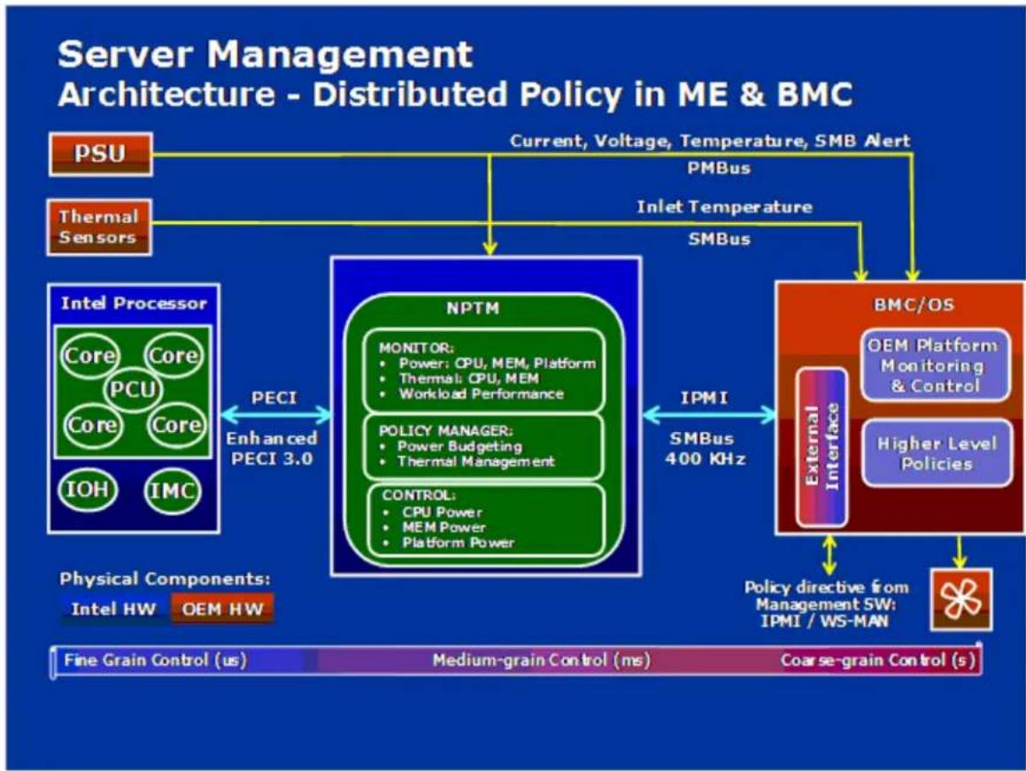
flowchart
graph TD
    A["PSU"] -->|Current, Voltage, Temperature, SMB Alert| B["NPTM"]
    C["Thermal Sensors"] -->|Inlet Temperature| B
    D["Intel Processor"] -->|PECI Enhanced PECI 3.0| B
    E["BMC/OS"] -->|IPMI SMBus 400 KHz| F["External Interface"]
    F --> G["Policy directive from Management SW: IPMI / WS-MAN"]
    H["Physical Components: Intel HW OEM HW"] --> I["Fine Grain Control (us)"]
    H --> J["Medium-grain Control (ms)"]
    H --> K["Coarse-grain Control (s)"]
    B --> L["MONITOR: Power: CPU, MEM, Platform; Thermal: CPU, MEM; Workload Performance"]
    B --> M["POLICY MANAGER: Power Budgeting; Thermal Management"]
    B --> N["CONTROL: CPU Power; MEM Power; Platform Power"]
    B --> O["BMC/OS"]
    style B fill:#99ccff,stroke:#333
    style F fill:#ffcccc,stroke:#333
Figure 20. Management Engine Distribution Model
4.14.3 ME System Management Bus (SMBus\*) Interface
- The ME uses the SMLink0 on the SSB in multi-master mode as a dedicated bus for communication with the BMC using the IPMB protocol. The BMC FW considers this a secondary IPMB bus and runs at 400 kHz.
- The ME uses the SMLink1 on the SSB in multi-master mode bus for communication with PMBus* devices in the power supplies for support of various NM-related features. This bus is shared with the BMC, which polls these PMBus* power supplies for sensor monitoring purposes (for example, power supply status, input power, and so on). This bus runs at 100 KHz.
- The Management Engine has access to the "Host SMBus*".
4.14.4 BMC - Management Engine Interaction
Management Engine-Integrated BMC interactions include the following:
- Integrated BMC stores sensor data records for ME-owned sensors.
- Integrated BMC participates in ME firmware update.
- Integrated BMC initializes ME-owned sensors based on SDRs.
- Integrated BMC receives platform event messages sent by the ME.
- Integrated BMC notifies ME of POST completion.
- BMC may be queried by the ME for inlet temperature readings.
4.14.5 ME Power and Firmware Startup
On Intel ^® Server Board S2600JF, the ME is on standby power. The ME FW begins its startup sequence at the same time when the BMC FW is booting. As the BMC FW is booting to a Linux* kernel and the ME FW uses an RTOS, the ME FW will always complete its basic initialization before the BMC. The ME FW can be configured to send a notification message to the BMC. After this point, the ME FW is ready to process any command requests from the BMC.
In S0/S1 power states, all ME FW functionality is supported. Some features, such as power limiting, are not supported in S3/S4/S5 power states. Refer to ME FW documentation for details on what is not supported while in the S3/S4/S5 states.
The ME FW uses a single operational image with a limited-functionality recovery image. In order to upgrade an operational image, a boot to recovery image must be performed. The ME FW does not support an IPMI update mechanism except for the case that the system is configured with a dual-ME (redundant) image. In order to conserve flash space, which the ME FW shares with BIOS, Intel® Server Boards and Systems only support a single ME image. For this case, ME update is only supported by means of BIOS performing a direct update of the flash component. The recovery image only provides the basic functionality that is required to perform the update; therefore other ME FW features are not functional when the update is in progress.
4.14.6 SmaRT/CLST
The power supply optimization provided by SmaRT/CLST relies on a platform HW capability as well as ME FW support. When a PMBus*-compliant power supply detects insufficient input voltage, an over current condition or an over temperature condition, it will assert the SMBAlert# signal on the power supply SMBus* (also known as the PMBus*). Through the use of external gates, this results in a momentary assertion of the PROCHOT# and MEMHOT# signals to the processors, thereby throttling the processors and memory. The ME FW also sees the SMBAlert# assertion, queries the power supplies to determine the condition causing the assertion, and applies an algorithm to either release or prolong the throttling, based on the situation.
System power control modes include:
- SmaRT: Low AC input voltage event; results in a one-time momentary throttle for each event to the maximum throttle state.
- Electrical Protection CLST: High output energy event; results in a throttling hiccup mode with fixed maximum throttle time and a fix throttle release ramp time.
- Thermal Protection CLST: High power supply thermal event; results in a throttling hiccup mode with fixed maximum throttle time and a fix throttle release ramp time.
When the SMBAlert# signal is asserted, the fans will be gated by HW for a short period (\~100ms) to reduce overall power consumption. It is expected that the interruption to the fans will be of short enough duration to avoid false lower threshold crossings for the fan tach sensors; however, this may need to be comprehended by the fan monitoring FW if it does have this side effect.
4.15 Other Platform Management
The platform supports the following sleep states, S1 and S5. Within S0, the platform supports additional lower power states, such as C1e and C6, for the CPU.
4.15.1 Wake On LAN (WOL)
- Wake On LAN (WOL) is supported on both LAN ports and IOM LAN modules for all supported Sleep states.
- Wake on Ring is supported on the external Serial port only for all supported Sleep states.
- Wake on USB is supported on the rear and front panel USB ports for S1 only.
- Wake on RTC is supported for all supported Sleep states.
- Wake IPMI command is supported (BMC function no additional hardware requirement) for all supported Sleep states.
4.15.2 PCI Express\* Power Management
L0 and L3 power management states are supported on all PCI Express* slots and embedded end points.
4.15.3 PMBus\*
Power supplies that have PMBus* 1.1 are supported and required to support Intel® Dynamic Power Node Manager. The Intel® Server Board S2600JF supports the features of Intel® Dynamic Power Node Manager version 1.5 except the inlet temperature sensor.
4.15.4 Node Power Policies
When working with Intel ^® Server Chassis H2000JF, the BMC on each node monitors its fans and temperature for critical failures. When there is a fan failure and a critical temperature event at the same time, the node will be powered down. When this occurs, the node needs to be manually powered back on.
Additionally on Intel ^® Server Board S2600JF, the BMC on node 3 and node 4 monitors for a power supply over current condition or power supply over temperature condition. If either of these occurs and the Shutdown Policy has been enabled, the node will be powered down. When this occurs, the node needs to be manually powered back on. However, if the over current or over temperature event is detected again, the node will be powered back off.
The Shutdown Policy setting is only shown on Node 3 and Node 4, and is disabled by default but can be enabled or disabled in the BIOS setup Server Management page or by using the Set Shutdown Policy command.
5. BIOS Setup Interface
5.1 HotKeys Supported during POST
Certain HotKeys are recognized during POST. A HotKey is a key or key combination that is recognized as an unprompted command input, that is, the operator is not prompted to press the HotKey and typically the HotKey will be recognized even while other processing is in progress.
The Intel ^® Server Board S2600JF Family BIOS recognizes a number of HotKeys during POST. After the OS is booted, HotKeys are the responsibility of the OS and the OS defines its own set of recognized HotKeys.
Following are the POST HotKeys with the functions they cause to be performed.
Table 26. POST HotKeys Recognized
| HotKey Combination | Function |
| Enter Setup | |
| Pop-up BIOS Boot Menu | |
| Network boot |
5.2 POST Logo/Diagnostic Screen
The logo/Diagnostic Screen displays in one of the two forms:
- If Quiet Boot is enabled in the BIOS setup, a logo splash screen is displayed. By default, Quiet Boot is enabled in the BIOS setup. If the logo is displayed during POST, press
to hide the logo and display the diagnostic screen. - If a logo is not present in the flash ROM or if Quiet Boot is disabled in the system configuration, the POST Diagnostic Screen is displayed with a summary of system configuration information.
The diagnostic screen displays the following information:
■ "Copyright
■ AMI Copyright statement
- BIOS version (ID)
■ BMC firmware version
- SDR version
■ ME firmware version
- Platform ID
- System memory detected (total size of all installed DDR3 DIMMs)
- Current memory speed (currently configured memory operating frequency)
- Processor information (Intel ^ Brand String identifying the type of processor and nominal operating frequency, and the number of physical processors identified)
■ Keyboards detected, if any attached
■ Mouse devices detected, if any attached
- Instructions showing hotkeys for going to Setup, going to pop-up Boot Menu, and starting Network Boot
5.3 BIOS Boot Pop-up Menu
The BIOS Boot Specification (BBS) provides a Boot Pop-up menu that can be invoked by pressing the
When an Administrator password is installed in Setup, the Administrator password will be required in order to access the Boot Pop-up menu using the
5.4 BIOS Setup Utility
The BIOS Setup utility is a text-based utility that allows the user to configure the system and view current settings and environment information for the platform devices. The Setup utility controls the platform's built-in devices, the boot manager, and error manager.
The BIOS Setup interface consists of a number of pages or screens. Each page contains information or links to other pages. The advanced tab in Setup displays a list of general categories as links. These links lead to pages containing a specific category's configuration.
The following sections describe the look and behavior for the platform setup.
5.4.1 BIOS Setup Operation
The BIOS Setup Utility has the following features:
- Localization – The Intel ^ Server Board BIOS is available only in English. However, BIOS Setup uses the Unicode standard and is capable of displaying data and input in Setup fields in all languages currently included in the Unicode standard.
- Console Redirection – BIOS Setup is functional through Console Redirection over various terminal emulation standards. This may limit some functionality for compatibility, for example, usage of colors or some keys or key sequences or support of pointing devices.
- Setup screens are designed to be displayable in an 80-character x 24-line format in order to work with Console Redirection, although that screen layout should display correctly on any format with longer lines or more lines on the screen.
- Password protection – BIOS Setup may be protected from unauthorized changes by setting an Administrative Password in the Security screen. When an Administrative Password has been set, all selection and data entry fields in Setup (except System Time and Date) are grayed out and cannot be changed unless the Administrative Password has been entered.
Note: If an Administrative Password has not been set, anyone who boots the system to Setup has access to all selection and data entry fields in Setup and can change any of them.
5.4.1.1 Setup Page Layout
The Setup page layout is sectioned into functional areas. Each occupies a specific area of the screen and has dedicated functionality. The following table lists and describes each functional area.
The Setup page is designed to a format of 80 x 24 (24 lines of 80 characters each). The typical display screen in a Legacy mode or in a terminal emulator mode is actually 80 characters by 25 lines, but with line wrap enabled (which it usually is) the 25^th line cannot be used with the Setup page.
Table 27. BIOS Setup Page Layout
| Functional Area | Description |
| Title (Tab) Bar | The Title Bar is located at the top of the screen and displays “Tabs” with the titles of the top-level pages, or screens that can be selected. Using the left and right arrow keys moves from page to page through the Tabs.When there are more Tabs than can be displayed on the Title (Tab) Bar, they will scroll off to the left or right of the screen and temporarily disappear from the visible Title Bar. Using the arrow keys will scroll them back onto the visible Title Bar. When the arrow keys reach either end of the Title Bar, they will “wrap around” to the other end of the Title Bar.For multi-level hierarchies, this shows only the top-level page above the page which the user is currently viewing. The Page Title gives further information. |
| Page Title | In a multi-level hierarchy of pages beneath one of the top-level Tabs, the Page Title identifying the specific page which the user is viewing is located in the upper left corner of the page. Using the(Escape) key will return the user to the higher level in the hierarchy, until the top-level Tab page is reached. |
| Setup Item List | The Setup Item List is a set of control entries and informational items. The list is displayed in two columns. For each item in the list:▪ The left column of the list contains Prompt String (or Label String), a character string that identifies the item. The Prompt String may be up to 34 characters long in the 80 x 24 page format.▪ The right column contains a data field that may be an informational data display, a data input field, or a multiple choice field. Data input or multiple-choice fields are demarcated by square brackets (“[....]”). This field may be up to 90 characters long, but only the first 22 characters can be displayed on the 80 x 24 page (24 characters for an informational display-only field).The operator navigates up and down the right hand column through the available input or choice fields.A Setup Item may also represent a selection to open a new screen with a further group of options for specific functionality. In this case, the operator navigates to the desired selection and presses(to go to the new screen. |
| Item-specific Help Area | The Item-specific Help Area is located on the right side of the screen and contains Help Text specific to the highlighted Setup Item. Help information may include the meaning and usage of the item, allowable values, effects of the options, and so on.The Help Area is a 29 character by 11 line section of the 80 x 24 page. The Help Text may have explicit line-breaks within it. When the text is longer than 29 characters, it is also broken to a new line, dividing the text at the last space (blank) character before the 29^th character. An unbroken string of more than 29 characters will be arbitrarily wrapped to a new line after the 29^th character. Text that extends beyond the end of the 11^th line will not be displayed. |
| Keyboard Command Area | The Keyboard Command Area is located at the bottom right of the screen and continuously displays help for keyboard special keys and navigation keys. |
5.4.1.2 Entering BIOS Setup
To enter the BIOS Setup using a keyboard (or emulated keyboard), press the
Press
When the Setup Utility is entered, the Main screen is displayed. However, serious errors cause the system to display the Error Manager screen instead of the Main screen.
It is also possible to cause a boot to Setup using an IPMI 2.0 command Get/Set System Boot Options. For details on that capability, see the explanation in the IPMI description.
5.4.1.3 Setup Navigation Keyboard Commands
The bottom right portion of the Setup screen provides a list of commands that are used to navigate through the Setup utility. These commands are displayed at all times.
Each Setup menu page contains a number of features. Each feature is associated with a value field, except those used for informative purposes. Each value field contains configurable parameters. Depending on the security option chosen and in effect by the password, a menu feature's value may or may not be changed. If a value cannot be changed, its field is made inaccessible and appears grayed out.
Table 28. BIOS Setup: Keyboard Command Bar
| Key | Option | Description |
| Execute Command | Thekey is used to activate submenus when the selected feature is a submenu, or to display a pick list if a selected option has a value field, or to select a subfield for multi-valued features such as time and date. If a pick list is displayed, thekey selects the currently highlighted item, undoes the pick list, and returns the focus to the parent menu. | |
| Exit | Thekey provides a mechanism for backing out of any field. When thekey is pressed while editing any field or selecting features of a menu, the parent menu is re-entered.When thekey is pressed in any submenu, the parent menu is re-entered. When thekey is pressed in any major menu, the exit confirmation window is displayed and the user is asked whether changes can be discarded. If “No” is selected and thekey is pressed, or if thekey is pressed, the users are returned to where they were beforewas pressed, without affecting any existing settings. If “Yes” is selected and thekey is pressed, the setup is exited and the BIOS returns to the main System Options Menu screen. | |
| ↑ | Select Item | The up arrow is used to select the previous value in a pick list, or the previous option in a menu item's option list. The selected item must then be activated by pressing thekey. |
| ↓ | Select Item | The down arrow is used to select the next value in a menu item's option list, or a value field's pick list. The selected item must then be activated by pressing thekey. |
| ↔ | Select Menu | The left and right arrow keys are used to move between the major menu pages. The keys have no effect if a submenu or pick list is displayed. |
| Select Field | Thekey is used to move between fields. For example,can be used to move from hours to minutes in the time item in the main menu. | |
| -+ | Change ValueChange Value | The minus key on the keypad is used to change the value of the current item to the previous value. This key scrolls through the values in the associated pick list without displaying the full list.The plus key on the keypad is used to change the value of the current menu item to the next value. This key scrolls through the values in the associated pick list without displaying the full list. On 106-key Japanese keyboards, the plus key has a different scan code than the plus key on the other keyboards, but has the same effect. |
| Setup Defaults | Pressing thekey causes the following message to display:Load Optimized Defaults?Yes NoIf “Yes” is highlighted andis pressed, all Setup fields are set to their default values. If “No” is highlighted andis pressed, or if thekey is pressed, the users are returned to where they were beforewas pressed without affecting any existing field values. | |
| Save and Exit | Pressing thekey causes the following message to display:Save configuration and reset?Yes NoIf “Yes” is highlighted andis pressed, all changes are saved and the Setup is exited. If “No” is highlighted andis pressed, or if thekey is pressed, the users are returned to where they were beforewas pressed without affecting any existing values. |
5.4.1.4 Setup Screen Menu Selection Bar
The Setup Screen Menu selection bar is located at the top of the BIOS Setup Utility screen. It displays tabs showing the major screen selections available to the user. By using the left and right arrow keys, the user can select the listed screens. Some screen selections are out of the visible menu space, and become available by scrolling to the left or right of the current selections displayed.
5.4.2 BIOS Setup Utility Screens
The following sections describe the screens available in the BIOS Setup utility for the configuration of the server platform.
For each of these screens, there is an image of the screen with a list of Field Descriptions that describe the contents of each item on the screen. Each item on the screen is hyperlinked to the relevant Field Description. Each Field Description is hyperlinked back to the screen image.
These lists follow the following guidelines:
- The text heading for each Field Description is the actual text as displayed on the BIOS Setup screen. This screen text is a hyperlink to its corresponding Field Description.
- The text shown in the Option Values and Help Text entries in each Field Description is the actual text and values are displayed on the BIOS Setup screens.
-
In the Option Values entries, the text for the default values is shown with an underline. These values do not appear underline on the BIOS Setup screen. The underlined text in this document is to serve as a reference to which value is the default value.
-
The Help Text entry is the actual text that appears on the screen to accompany the item when the item is the one in focus (active on the screen).
- The Comments entry provides additional information where it may be helpful. This information does not appear on the BIOS Setup screens.
- Information enclosed in angular brackets (< >) in the screen shots identifies text that can vary, depending on the options installed. For example,
is replaced by the actual value for "Total Memory". - Information enclosed in square brackets ([ ]) in the tables identifies areas where the user must type in text instead of selecting from a provided option.
- Whenever information is changed (except Date and Time), the system requires a save and reboot to take place in order for the changes to take effect. Alternatively, pressing
discards the changes and resumes POST to continue to boot the system according to the boot order set from the last boot.
5.4.2.1 Map of Screens and Functionality
There are a number of screens in the entire Setup collection. They are organized into major categories. Each category has a hierarchy beginning with a top-level screen from which lower-level screens may be selected. Each top-level screen appears as a tab, arranged across the top of the Setup screen image of all top-level screens.
There are more categories than will fit across the top of the screen, so at any given time there will be some categories which will not appear until the user has scrolled across the tabs which are present.
The categories and the screens included in each category are listed as follows, with links to each of the screens named.
Table 29. Screen Map
| Categories (Top Tabs) | Second Level Screens | Third Level Screens |
| Main Screen (Tab) | ||
| Advanced Screen (Tab) | ||
| Processor Configuration | ||
| Power and Performance | ||
| Memory Configuration | ||
| Memory RAS and Performance Configuration | ||
| Mass Storage Controller Configuration | ||
| PCI Configuration | ||
| NIC Configuration | ||
| UEFI Network Stack | ||
| UEFI Option ROM Control | ||
| Processor PCIe Link Speed | ||
| Serial Port Configuration | ||
| USB Configuration | ||
| System Acoustic and Performance Configuration | ||
| Security Screen (Tab) | ||
| Server Management Screen (Tab) | ||
| Console Redirection | ||
| System Information | ||
| BMC LAN Configuration | ||
| Boot Options Screen (Tab) | ||
| CDROM Order | ||
| Hard Disk Order | ||
| Floppy Order | ||
| Network Device Order | ||
| BEV Device Order | ||
| Add EFI Boot Option | ||
| Delete EFI Boot Option | ||
| Boot Manager Screen (Tab) | ||
| Error Manager Screen (Tab) | ||
| Save and Exit Screen (Tab) |
5.4.2.2 Main Screen (Tab)
The Main Screen is the first screen that appears when the BIOS Setup configuration utility is entered, unless an error has occurred. If an error has occurred, the Error Manager Screen appears instead.
| Main | Advanced | Security | Server Management | Boot Options | Boot Manager |
| Logged in as: | Administrator/User | ||||
| Platform ID | |||||
| System BIOS | |||||
| BIOS Version | |||||
| Build Date | |||||
| Memory | |||||
| Total Memory | |||||
| Quiet Boot | Enabled/Disabled | ||||
| POST Error Pause | Enabled/Disabled | ||||
| System Date | [Day MM/DD/YYYY] | ||||
| System Time | [HH:MM:SS] |
Figure 21. Main Screen
Table 30. Setup Utility – Main Screen Fields
| Setup Item | Options | Help Text | Comments |
| Logged in as | Information only. Displays password level that setup is running in: Administrator or User. With no passwords set, Administrator is the default mode. | ||
| Platform ID | S2600JF | Information only. Displays the Platform ID: S2600JF. | |
| System BIOS | |||
| BIOS Version | Information only. Displays the current BIOS version.xx = major release versionyy = minor release versionzzzz = release number | ||
| Build Date | Information only. Displays the current BIOS build date. | ||
| Memory | |||
| Total Memory | Information only. Displays the total physical memory installed in the system, in MB or GB.The term physical memory indicates the total memory discovered in the form of installed DDR3 DIMMs. | ||
| Quiet Boot | EnabledDisabled | [Enabled] – Display the logo screen during POST.[Disabled] – Display the diagnostic screen during POST. | |
| POST Error Pause | EnabledDisabled | [Enabled] – Go to the Error Manager for critical POST errors.[Disabled] – Attempt to boot and do not go to the Error Manager for critical POST errors. | If enabled, the POST Error Pause option takes the system to the error manager to review the errors when major errors occur. Minor and fatal error displays are not affected by this setting. |
| System Date | [Day of week MM/DD/YYYY] | System Date has configurable fields for Month, Day, and Year.Use [Enter] or [Tab] key to select the next field.Use [+] or [-] key to modify the selected field. | |
| System Time | [HH:MM:SS] | System Time has configurable fields for Hours, Minutes, and Seconds.Hours are in 24-hour format.Use [Enter] or [Tab] key to select the next field.Use [+] or [-] key to modify the selected field. | |
5.4.2.3 Advanced Screen (Tab)
The Advanced screen provides an access point to configure several groups of options. On this screen, the user can select the option group to be configured. Configuration actions are performed on the selected screen, and not directly on the Advanced screen.
To access this screen from the Main screen or other top-level Tab screen, press the right or left arrow key to traverse the tabs at the top of the Setup screen until the Advanced screen is selected.
| Main | Advanced | Security | Server Management | Boot Options | Boot Manager |
| ► Processor Configuration | |||||
| ► Power & Performance | |||||
| ► Memory Configuration | |||||
| ► Mass Storage Controller Configuration | |||||
| ► PCI Configuration | |||||
| ► Serial Port Configuration | |||||
| ► USB Configuration | |||||
| ► System Acoustic and Performance Configuration | |||||
Figure 22. Advanced Screen
Table 31. Setup Utility – Advanced Screen Fields
| Setup Item | Help Text |
| Processor Configuration | View/Configure processor information and settings. |
| Power and Performance | View/Configure power and performance policy. |
| Memory Configuration | View/Configure memory information and settings. |
| Mass Storage Controller Configuration | View/Configure mass storage controller information and settings. |
| PCI Configuration | View/Configure PCI information and settings. |
| Serial Port Configuration | View/Configure serial port information and settings. |
| USB Configuration | View/Configure USB information and settings. |
| System Acoustic and Performance Configuration | View/Configure system acoustic and performance information and settings. |
5.4.2.4 Processor Configuration
The Processor Configuration screen displays the processor identification and microcode level, core frequency, cache sizes, Intel® QuickPath Interconnect information for all processors currently installed. It also allows the user to enable or disable a number of processor options.
To access this screen from the Main screen, select Advanced > Processor Configuration. To move to another screen, press the
Advanced
Processor Configuration
| Processor Socket | CPU 1 | CPU 2 |
| Processor ID | * | |
| Microcode Frequency | ||
| Microcode Revision | ||
| L1 Cache RAM | ||
| L2 Cache RAM | ||
| L3 Cache RAM | ||
| Processor 1 Version | ||
| Processor 2 Version | ||
| Current Intel® QPI Link Speed | Slow/Fast | |
| Intel® QPI Link Frequency | Unknown GT/s/6.4 GT/s/7.2 GT/s/8.0 GT/s | |
| Intel® QPI Frequency Select | Auto Max/6.4 GT/s/7.2 GT/s/8.0 GT/s | |
| Intel® Turbo Boost Technology | Enabled/Disabled | |
| Enhanced Intel SpeedStep® Tech | Enabled/Disabled | |
| Processor C3 | Enabled/Disabled | |
| Processor C6 | Enabled/Disabled | |
| Intel® Hyper-Threading Tech | Enabled/Disabled | |
| Active Processor Cores | All/1/2/3/4/5/6/7/8/9 | |
| Execute Disable Bit | Enabled/Disabled | |
| Intel® Virtualization Technology | Enabled/Disabled | |
| Intel® VT for Direct I/O | Enabled/Disabled | |
| Enhanced Error Containment Mode | Enabled/Disabled | |
| MLC Streamer | Enabled/Disabled | |
| MLC Spatial Prefetcher | Enabled/Disabled | |
| DCU Data Prefetcher | Enabled/Disabled | |
| DCU Instruction Prefetcher | Enabled/Disabled | |
| Direct Cache Access (DCA) | Enabled/Disabled | |
| Extended ATR | 0x03/0x01 | |
| PFloor Tuning | 12 | |
| SMM Wait Timeout | [20 - 3000ms, 20 is default] | |
Figure 23. Processor Configuration Screen
Table 32. Setup Utility – Processor Configuration Screen Fields
| Setup Item | Options | Help Text | Comments |
| Processor ID | Information only. Processor CPUID. | ||
| Processor Frequency | Information only. Current frequency of the processor. | ||
| Microcode Revision | Information only. Revision of the loaded microcode. | ||
| L1 Cache RAM | Information only. Size of the Processor L1 Cache. | ||
| L2 Cache RAM | Information only. Size of the Processor L2 Cache. | ||
| L3 Cache RAM | Information only. Size of the Processor L3 Cache. | ||
| Processor Version | Information only. ID string from the Processor. | ||
| Processor 1 Version | Information only. Brand ID string of the processor with CPUID instruction. | ||
| Processor 2 Version | Information only. Brand ID string of the processor with CPUID instruction. | ||
| Current QPI Link Speed | Information only. Current speed that the QPI Link is using. | ||
| QPI Link Frequency | Information only. Current frequency that the QPI Link is operating. | ||
| Current QPI Frequency Select | Auto Max6.4 GT/s7.2 GT/s8.0 GT/s | Allows for selecting the Intel® QuickPath Interconnect Frequency. Recommended to leave in [Auto Max] so that the BIOS can select the highest common Intel® QuickPath Interconnect frequency. | Lowering the QPI frequency may improve performance per watt for some processing loads and on certain benchmarks. [Auto Max] will give the maximum QPI performance available. Appears only on multi-socket boards.When a multi-socket board has only one processor installed, this will be grayed out, with the previous value remaining displayed.Changes in QPI Link Frequency will not take effect until the system reboots, so this will not immediately change the QPI Link Frequency display. Changing QPI Link Frequency does not affect the QPI Link Speed. |
| Intel® Turbo Boost Technology | EnabledDisabled | Intel® Turbo Boost Technology allows the processor to automatically increase its frequency if it is running below power, temperature, and current specifications. | This option is visible only if the processor in the system supports Intel® Turbo Boost Technology. |
| Enhanced Intel SpeedStep® Technology | EnabledDisabled | Enhanced Intel SpeedStep® Technology allows the system to dynamically adjust processor voltage and core frequency, which can result in decreased average power consumption and decreased average heat production.Contact your OS vendor regarding OS support of this feature. | When Disabled, the processor setting reverts to running at Max TDP Core Frequency (rated frequency). |
| Processor C3 | EnabledDisabled | Enable/Disable Processor C3 (ACPI C2/C3) report to OS. | This is normally Disabled, but can be Enabled for improved performance on certain benchmarks and in certain situations. |
| Processor C6 | EnabledDisabled | Enable/Disable Processor C6 (ACPI C3) report to OS. | This is normally Enabled, but can be Disabled for improved performance on certain benchmarks and in certain situations. |
| Intel® Hyper-Threading Technology | EnabledDisabled | Intel® HT Technology allows multithreaded software applications to execute threads in parallel within each processor.Contact your OS vendor regarding OS support of this feature. | This option is visible only if all processors installed in the system support Intel® Hyper-Threading Technology. |
| Active Processor Cores | All1234567 | Number of cores to enable in each processor package. | The number of cores that appear as selections depends on the number of cores available in the processors installed. Boards may have as many as 8 cores in each of 1, 2, or 4 processors. The same number of cores must be active in each processor package. |
| Execute Disable Bit | EnabledDisabled | Execute Disable Bit can help prevent certain classes of malicious buffer overflow attacks. | This option is visible only if all processors installed in the system support the Execute Disable Bit. The OS and applications installed must support this feature in order for it to be enabled. |
| Intel® Virtualization Technology | EnabledDisabled | Intel® Virtualization Technology allows a platform to run multiple operating systems and applications in independent partitions.Note:A change to this option requires the system to be powered off and then back on before the setting takes effect. | This option is visible only if all processors installed in the system support Intel® VT. The software configuration installed on the system must support this feature in order for it to be enabled. |
| Intel® Virtualization Technology for Directed I/O | EnabledDisabled | Enable/Disable Intel®Virtualization Technology for Directed I/O (Intel® VT-d).Report the I/O device assignment to VMM through DMAR ACPI Tables. | This option is visible only if all processors installed in the system support Intel® VT-d. The software configuration installed on the system must support this feature in order for it to be enabled. |
| Enhanced Error Containment Mode | EnabledDisabled | Enhanced Error Containment (Data Poisoning) is not supported by all models of processors, and this option will not appear unless all installed processors support Enhanced Error Containment. This option globally enables or disables both Core and Uncore Data Poisoning, for processors which support them. | |
| MLC Streamer | EnabledDisabled | MLC Streamer is a speculative prefetch unit within the processors. | MLC Streamer is normally Enabled for best efficiency in L2 Cache and Memory Channel use, but disabling it may improve performance for some processing loads and on certain benchmarks. |
| MLC Spatial Prefetcher | EnabledDisabled | [Enabled] – Fetches adjacent cache line (128 bytes) when required data is not currently in cache.[Disabled] – Only fetches cache line with data required by the processor (64 bytes). | MLC Spatial Prefetcher is normally Enabled for best efficiency in L2 Cache and Memory Channel use, but disabling it may improve performance for some processing loads and on certain benchmarks. |
| DCU Data Prefetcher | EnabledDisabled | The next cache line will be prefetched into L1 data cache from L2 or system memory during unused cycles if it sees that the processor core has accessed several bytes sequentially in a cache line as data.[Disabled] – Only fetches cache line with data required by the processor (64 bytes). | DCU Data Prefetcher is normally Enabled for best efficiency in L1 Data Cache and Memory Channel use, but disabling it may improve performance for some processing loads and on certain benchmarks. |
| DCU Instruction Prefetcher | EnabledDisabled | The next cache line will be prefetched into L1 instruction cache from L2 or system memory during unused cycles if it sees that the processor core has accessed several bytes sequentially in a cache line as data. | DCU Instruction Prefetcher is normally Enabled for best efficiency in L1 I Cache and Memory Channel use, but disabling it may improve performance for some processing loads and on certain benchmarks. |
| Direct Cache Access (DCA) | EnabledDisabled | Allows processors to increase the I/O performance by placing data from I/O devices directly into the processor cache. | System performance is usually best with Direct Cache Access Enabled. In certain unusual cases, disabling this may give improved results. |
| Extended ATR | 0x030x01 | Extended Timeout value for PCIe tuning. 0x03 = default timeout. 0x01 = extended timeout. | Adjust ATR value for PCIe performance improvement. |
| PFloor Tuning | 12 | Adjustment CPU idle frequency for PCIe Bus tuning between 12 and 3 less than CPU rated frequency. | Adjustment of CPU idle frequency for PCIe performance tuning. |
| SMM Wait Timeout | 20 | Millisecond timeout waiting for BSP and SPs to enter SMM. Range is 20ms to 3000ms. | Amount of time to allow for the SMI Handler to respond to an SMI. If exceeded, the BMC generates an SMI Timeout and resets the system. |
5.4.2.5 Power and Performance Policy
The Power and Performance screen allows the user to specify a profile which is optimized in the direction of either reduced power consumption or increased performance.
To access this screen from the Main screen, select Advanced > Power and Performance. To move to another screen, press the
Advanced
Power & Performance
Power and Performance Policy
Performance / Balanced Performance / Balanced Power / Power
[Performance] Optimization is strongly toward performance, even at the expense of energy efficiency.
[Balanced Performance] Weights optimization toward performance, while conserving energy.
[Balanced Power] Weights optimization toward energy conservation, with good performance.
[Power] Optimization is strongly toward energy efficiency, even at the expense of performance.
Figure 24. Power and Performance Configuration Screen
Table 33. Setup Utility – Power and Performance Configuration Screen Fields
| Setup Item | Options | Comments |
| CPU Power and Performance Policy | Performance | Optimization is strongly toward performance, even at the expense of energy efficiency. |
| Balanced Performance | Weights optimization toward performance, while conserving energy. | |
| Balanced Power | Weights optimization toward energy conservation, with good performance. | |
| Power | Optimization is strongly toward energy efficiency, even at the expense of performance. |
When the user selects a Power and Performance Policy in Setup, there is a list of complementary settings which are made. These can be individually overridden after the policy setting has been selected and the profile settings performed. The profile settings are listed in the following table.
Table 34. Power/Performance Profiles
| BIOS Features | Available Settings | Performance | Balanced Performance | Balanced Power | Power |
| Setup: Advanced > Power and Performance | |||||
| CPU Power and Performance Policy | Performance/Balanced Performance/Balanced Power/Power | Performance | (Balanced Performance) | Balanced Power | Power |
| Setup: Advanced > Processor Configuration | |||||
| Intel® QPI Frequency Select | Auto Max/6.4 GT/s/7.2 GT/s/8.0 GT/s | (Auto Max) | (Auto Max) | (Auto Max) | 6.4 GT/s |
| Intel® Turbo Boost Technology | Enabled/Disabled | (Enabled) | (Enabled) | (Enabled) | (Enabled) |
| Enhanced Intel SpeedStep® Technology | Enabled/Disabled | (Enabled) | (Enabled) | (Enabled) | (Enabled) |
| Processor C3 | Enabled/Disabled | (Disabled) | (Disabled) | (Disabled) | (Disabled) |
| Processor C6 | Enabled/Disabled | (Enabled) | (Enabled) | (Enabled) | (Enabled) |
| Intel® Hyper Threading | Enabled/Disabled | (Enabled) | (Enabled) | (Enabled) | (Enabled) |
| Active Processor Cores | All/1/2/3/4/5/6/7 | (All) | (All) | (All) | (All) |
| MLC Streamer | Enabled/Disabled | (Enabled) | (Enabled) | (Enabled) | (Enabled) |
| MLC Spatial Prefetcher | Enabled/Disabled | (Enabled) | (Enabled) | (Enabled) | (Enabled) |
| DCU Data Prefetcher | Enabled/Disabled | (Enabled) | (Enabled) | (Enabled) | (Enabled) |
| DCU Instruction Prefetcher | Enabled/Disabled | (Enabled) | (Enabled) | (Enabled) | (Enabled) |
| Direct Cache Access (DCA) | Enabled/Disabled | (Enabled) | (Enabled) | (Enabled) | (Enabled) |
| Setup: Advanced > Memory Configuration | |||||
| Memory Operating Speed Selection | Auto/800/1067/1333/1600 | (Auto) | (Auto) | (Auto) | (Auto) |
| Patrol Scrub | Enabled/Disabled | (Enabled) | (Enabled) | (Enabled) | (Enabled) |
| Demand Scrub | Enabled/Disabled | (Enabled) | (Enabled) | (Enabled) | (Enabled) |
| Memory Power Optimization | Power Optimized/Perform ance Optimized | (Performance Optimized) | (Performance Optimized) | (Performance Optimized) | (Performance Optimized) |
| Setup: Advanced > Memory Configuration > Memory RAS and Performance Configuration | |||||
| NUMA Optimized | Enabled/Disabled | (Enabled) | (Enabled) | (Enabled) | (Enabled) |
| Setup: Advanced > System Acoustic and Performance Configuration | |||||
| Set Throttling Mode | Auto/DCLTT/SCLTT/SOLTT | (Auto) | (Auto) | (Auto) | (Auto) |
| Set Fan Profile | Performance /Acoustic | (Performance) | (Performance) | (Performance) | (Performance) |
| Quiet Fan Idle Mode | Enabled/Disabled | (Disabled) | (Disabled) | (Disabled) | (Disabled) |
| Setup: Server Management | |||||
| EuP LOT6 OFF-Mode | Enabled/Disabled | (Disabled) | (Disabled) | (Disabled) | (Disabled) |
| Internal BIOS Settings not displayed in BIOS Setup | |||||
| QPI Link L0S enable | Auto/Enabled /Disabled | Disabled | (Auto) | (Auto) | (Auto) |
| CKE Throttling | Auto/Enabled /Disabled | Disabled | (Auto) | (Auto) | Enabled |
| Memory Voltage | Auto/1.5V/1.35V | 1.5v | (Auto) | (Auto) | (Auto) |
| CPU PkgC State Limit | Disabled/C6 with no retention/C6 with retention | Disabled | (C6 with retention) | (C6 with retention) | (C6 with retention) |
| Processor C1 mapped to ACPI C1 | Enabled/Disabled | (Enabled) | (Enabled) | (Enabled) | (Enabled) |
| Processor C6 with retention mapped to ACPI C2 | Enabled/Disabled | (Enabled) | (Enabled) | (Enabled) | (Enabled) |
| ACPI C3 | Enabled/Disabled | (Disabled) | (Disabled) | (Disabled) | (Disabled) |
| Processor C1/C3 Auto Demotion | Enabled/Disabled | (Enabled) | (Enabled) | (Enabled) | (Enabled) |
| Processor C1/C3 UnDemotion | Enabled/Disabled | (Enabled) | (Enabled) | (Enabled) | (Enabled) |
| ENERGY_PERF_BIAS mode | Performance/Balanced Performance/Balanced Power/Power | Performance | (Balanced Performance) | Balanced Power | Power |
5.4.2.6 Memory Configuration
The Memory Configuration screen allows the user to view details about the DDR3 DIMMs that are installed as system memory.
To access this screen from the Main screen, select Advanced > Memory Configuration. To move to another screen, press the
Advanced
Memory Configuration
| Total Memory | |
| Effective Memory | |
| Current Configuration | |
| Current Memory Speed | |
| Memory Operation Speed Selection | Auto/800/1066/1333/1600/1867 |
| Phase Shedding | Enabled/Disabled |
| Memory SPD Override | Enabled/Disabled |
| Patrol Scrub | Enabled/Disabled |
| Demand Scrub | Enabled/Disabled |
| Correctable Error Threshold | 20/10/5/Every |
▶ Memory RAS and Performance Configuration
DIMM Information
| DIMM_A1 | |
| DIMM_B1 | |
| DIMM_C1 | |
| DIMM_D1 | |
| DIMM_E1 | |
| DIMM_F1 | |
| DIMM_G1 | |
| DIMM_H1 |
Figure 25. Memory Configuration Screen
Table 35. Setup Utility – Memory Configuration Screen Fields
| Setup Item | Options | Comments |
| Total Memory | Information only. The amount of memory available in the system in the form of installed DDR3 DIMMs in units of GB. | |
| Effective Memory | Information only. The amount of memory available to the operating system in MB or GB.The Effective Memory is the difference between the Total Physical Memory and the sum of all memory reserved for internal usage, RAS redundancy, and SMRAM. This difference includes the sum of all DDR3 DIMMs that failed Memory BIST during POST, or were disabled by the BIOS during memory discovery phase to optimize memory configuration. | |
| Current Configuration | Independent ChannelMirrorLockstep | Displays one of the following:Independent Channel – DIMMs are operating in Independent Channel Mode, the default configuration when there is no RAS Mode configured.Mirror – Mirroring RAS Mode has been configured and is operational.Lockstep– Lockstep RAS Mode has been configured and is operational. |
| Current Memory Speed | Information only. Displays the speed the memory is running at. | |
| Memory Operating Speed Selection | Auto8001066133316001867 | Allows the user to select a specific speed at which memory will operate. Only speeds that are legitimate are available, that is, the user can only specify speeds less than or equal to the auto-selected Memory Operating Speed. The default Auto setting will select the highest achievable Memory Operating Speed consistent with the DIMMs and processors installed.Note: 1867 and 1600LV are supported only when Memory SPD Override is enabled. |
| Phase Shedding | EnabledDisabled | Enable/Disable DDR3 VR Static Phase Shedding. When Enabled, DDR3 VR can be automatically adjusted by typical load. |
| Memory SPD Override | EnabledDisabled | When enabled, it extends the platform's capability to support higher Memory Frequency to 1867MHz DIMM and 1600MHz LVDIMM with the Intel® S1600/S2600/S4600 family processors. |
| Patrol Scrub | EnabledDisabled | When enabled, Patrol Scrub is initialized to read through all of memory in a 24-hour period, correcting any Correctable ECC Errors it encounters by writing back the corrected data to memory. |
| Demand Scrub | EnabledDisabled | When enabled, Demand Scrub automatically corrects a Correctable ECC Error encountered during a fetch from memory by writing back the corrected data to memory. |
| Correctable Error Threshold | 20105AllNone | Specifies how many Correctable Errors must occur before triggering the logging of a SEL Correctable Error Event. Only the first threshold crossing is logged, unless “All” is selected. “All” causes every CE that occurs to be logged. “None” suppresses CE logging completely. |
| DIMM_XY | Displays the state of each DIMM socket present on the board. Each DIMM socket field reflects one of the following possible states:Operational– There is a DDR3 DIMM installed and operational in this slot.Not Installed– There is no DDR3 DIMM installed in this slot. Failed– The DIMM installed in this slot has failed during initialization. Disabled– The DIMM installed in this slot was disabled during initialization.For each DIMM that is in an Operational status, the size in GB of that DIMM is displayed.Note:X denotes the Channel Identifier and Y denotes the DIMM Identifier within the Channel. |
5.4.2.7 Memory RAS and Performance Configuration
The Memory RAS and Performance Configuration screen allows the user to customize several memory configuration options, such as whether to use Memory Mirroring or Memory Sparing.
To access this screen from the Main screen, select Advanced > Memory Configuration > Memory RAS and Performance Configuration. To move to another screen, press the
| Advanced | |
| Memory RAS and Performance Configuration | |
| Capabilities | |
| Memory Mirroring Possible | Yes/No |
| Memory Rank Sparing Possible | Yes/No |
| Memory Lockstep Possible | Yes/No |
| Select Memory RAS Configuration | Maximum Performance/Mirroring/Lockstep |
| NUMA Optimized | Disabled / Enabled |
Figure 26. Memory RAS and Performance Configuration Screen
Table 36. Setup Utility – Memory RAS and Performance Configuration Screen Fields
| Setup Item | Options | Help Text | Comments |
| Memory Mirroring Possible | YesNo | Information only. Displays whether the current DIMM configuration is capable of Memory Mirroring. | |
| Memory Rank Sparing Possible | YesNo | Information only. Displays whether the current DIMM configuration is capable of Rank Sparing. | |
| Memory Lockstep Possible | YesNo | Information only. Displays whether the current DIMM configuration is capable of Memory Lockstep. | |
| Select Memory RAS Configuration | Maximum PerformanceMirroringLockstep | Allows the user to select the memory RASConfiguration to be applied for the next boot. | Available modes depend on the current memory population. Modes that are not listed as “possible” are not available as choices. If the only valid choice is “Maximum Performance”, this option is grayed out and unavailable. |
| NUMA Optimized | EnabledDisabled | If enabled, the BIOS includes ACPI tables that are required for NUMA-aware Operating Systems. | This option is only present for boards that have two or more processor sockets. When a multi-socket board has only a single processor installed, this option is grayed out and set as Disabled. |
5.4.2.8 Mass Storage Controller Configuration
The Mass Storage Controller Configuration screen allows the user to configure the Mass Storage controllers that are integrated into the server board on which the BIOS is executing.
To access this screen from the Main screen, select Advanced > Mass Storage Controller Configuration. To move to another screen, press the
| Advanced | |
| Mass Storage Controller Configuration | |
| AHCI Controller Configuration | 2 ports of 6Gb/s SATA |
| SATA/SAS Controller Configuration | 4 ports in SAS mode |
| AHCI Capable SATA Controller | Disable/Compatibility/Enhanced/AHCI/RAID Mode |
| AHCI HDD Staggered Spin-Up | ENABLED/DISABLED |
| SAS/SATA Capable Controller | DISABLED/INTEL® ESRT2(LSI*)/INTEL® RSTE |
| Intel® Storage Module --- None / | |
| SATA Port 0 | Not Installed/<Drive Info.> |
| SATA Port 1 | Not Installed/<Drive Info.> |
Figure 27. Mass Storage Controller Configuration Screen
Table 37. Setup Utility – Mass Storage Controller Configuration Screen Fields
| Setup Item | Options | Help Text | Comments |
| AHCI Controller Configuration | Information only. | ||
| SATA/SAS Controller Configuration | Information only. | ||
| AHCI Capable SATA Controller | Disabled Compatibility Enhanced AHCI RAID Mode | Compatibility: Provides PATA emulation on the SATA device. Enhanced: Provides Native SATA support. AHCI: Enables the Advanced Host Controller Interface, which provides Enhanced SATA functionality. RAID Mode: Provides host-based RAID support on the on-board SATA ports. | This option configures the on-board AHCI-capable SATA controller, which is distinct from the SCU. |
| AHCI HDD Staggered Spin-Up | DisabledEnabled | If enabled for the AHCI Capable SATA controller, Staggered Spin-Up will be performed on drives attached to it. Otherwise these drives will all spin up at boot. | This option selects the target HDDs that will spin up at system boot. |
| SAS/SATA Capable Controller | DisabledIntel® ESRT2 (LSI*)Intel® RSTe | Intel® ESRT2: Provides host-based RAID 0/1/10 and optional RAID 5. Uses Intel® ESRT2 drivers (based on LSI* MegaSR).Intel® RSTe: Provides pass-through drive support. Also provides host-based RAID 0/1/10 support, and RAID 5 (in SATA mode only). Uses Intel® RSTe iaStor drivers. | This option selects the RAID stack to be used with the SCU. If Disabled is selected, any drives connected to the SCU will not be usable. |
| Intel® Storage Module | --- None | Information only. | |
| SATA Port x | Not InstalledDrive Info | Ports 0-1: 6Gb SATA capable port | Information only. This is repeated for all six SATA ports for the On-board SATA Controller. This section for SATA Drive Information does not appear when the SATA Mode is RAID Mode. |
5.4.2.9 PCI Configuration
The PCI Configuration screen allows the user to configure the PCI memory space used for on-board and add-in adapters, configure video options, and configure on-board adapter options. It also displays the NIC MAC Addresses currently in use.
To access this screen from the Main screen, select Advanced > PCI Configuration. To move to another screen, press the
| PCI Configuration | |
| Maximize Memory below 4GB | Enabled / Disabled |
| Memory Mapped I/O above 4GB | Enabled / Disabled |
| Memory Mapped I/O Size | Auto / 1G / 2G / 4G / 8G / 16G / 32G / 64G / 128G / 256G / 512G / 1024G |
| Onboard Video | Enabled / Disabled |
| Legacy VGA Socket | CPU Socket 1 / CPU Socket 2 |
| Dual Monitor Video | Enabled / Disabled |
| NTB PCIe Port on CPU Socket 1 | Transparent Bridge / NTB to NTB / NTB to RP |
| NTB PCIe Port on CPU Socket 2 | Transparent Bridge / NTB to NTB / NTB to RP |
| ▶ NIC Configuration | |
| ▶ UEFI Network Stack | |
| ▶ UEFI Option ROM Control | |
| ▶ Processor PCIe Link Speed | |
Figure 28. PCI Configuration Screen
Table 38. Setup Utility – PCI Configuration Screen Fields
| Setup Item | Options | Help Text | Comments |
| Maximize Memory below 4GB | EnabledDisabled | The BIOS maximizes memory usage below 4GB for an OS without PAE support, depending on the system configuration. Only enabled for an OS without PAE support. | When this option is enabled, the BIOS makes as much memory available as possible in the 32-bit (4GB) address space, by limiting the amount of PCI/PCIe Memory Address Space and PCIe Extended Configuration Space. This option is enabled only for a 32-bit OS without PAE capability or without PAE enabled. |
| Memory Mapped I/O above 4GB | EnabledDisabled | Enable or disable memory mapped I/O of 64-bit PCI devices to 4 GB or greater address space. | When enabled, PCI/PCIe Memory Mapped I/O for devices capable of 64-bit addressing is allocated to address space above 4GB, in order to allow larger allocations and avoid impacting address space below 4GB. |
| Memory Mapped I/O Size | Auto / 1G / 2G / 4G / 8G / 16G / 32G / 64G / 128G / 256G / 512G / 1024G | Set MMIO Size. | Auto → 2GB (Default). |
| Onboard Video | EnabledDisabled | On-board video controller.Warning: System video is completely disabled if this option is disabled and an add-in video adapter is not installed. | When disabled, the system requires an add-in video card in order for the video to be seen. |
| Legacy VGA Socket | CPU Spcket 1CPU Socket 2 | Determines whether Legacy VGA video output is enabled for PCIe slots attached to Processor Socket 1 or 2. Socket 1 is the default. | This option is necessary when using an add-in video card on a PCIe slot attached to CPU Socket 2, due to a limitation of the processor IIO. The Legacy video device can be connected through either socket, but there is a setting that must be set on only one of the two. This option allows the switch to use a video card in a slot connected to CPU Socket 2. |
| Dual Monitor Video | EnabledDisabled | If enabled, both an on-board video controller and an add-in video adapter are enabled for system video. The on-board video controller becomes the primary video device. | This option must be enabled to use an add-in card as a secondary POST Legacy Video device while also displaying on the On-board Video device.If there is no add-in video card in any PCIe slot connected to CPU Socket 1, this option is set to Disabled and grayed out and unavailable. |
| NTB PCIe Port on CPU Socket 1 | Transparent Bridge / NTB to NTB / NTB to RP | Configure CPU PCIe root port 3A as transparent bridge, or NTB to NTB, or NTB to Root Port. | Default is Transparent Bridge (NTB is disabled). |
| NTB PCIe Port on CPU Socket 2 | Transparent Bridge / NTB to NTB / NTB to RP | Configure CPU PCIe root port 3A as transparent bridge, or NTB to NTB, or NTB to Root Port. | Default is Transparent Bridge (NTB is disbaled). |
| NIC Configuration | View/Configure NIC information and settings. | ||
| UEFI Network Stack | View/Configure UEFI Network Stack Settings. | ||
| UEFI Option ROM Control | View/Configure UEFI Option ROM Control. | ||
| Processor PCIe Link Speed | View/Configure Processor PCIe Link Speed. |
5.4.2.10 NIC Configuration
The NIC Configuration screen allows the user to configure on-board NIC port 1 and port 2.
Advanced
NIC Configuration
Wake On LAN
Enabled / Disabled
PXE 1GbE Option ROM
Enabled / Disabled
iSCSI 1GbE / 10GbE Option ROM
Enabled / Disabled
Onboard NIC1 Type
NIC1 Controller
Enabled / Disabled
NIC1 Port1
Enabled / Disabled
NIC1 Port2
Enabled / Disabled
NIC1 Port1 PXE
Enabled / Disabled
NIC1 Port2 PXE
Enabled / Disabled
NIC1 Port1 MAC Address
NIC1 Port2 MAC Address
Onboard NIC2 Type
NIC2 InfiniBand Option ROM
Enabled / Disabled
NIC2 Port1 GUID
NIC2 Port1 MAC Address
IO Module 1 Type
IOM1 Port1 PXE
Enabled / Disabled
IOM1 Port2 PXE
Enabled / Disabled
IOM1 Port3 PXE
Enabled / Disabled
IOM1 Port4 PXE
Enabled / Disabled
IOM1 Port1 MAC Address
IOM1 Port2 MAC Address
IOM1 Port3 MAC Address
IOM1 Port4 MAC Address
IO Module 1 Type
IOM1 InfiniBand Option ROM
Enabled / Disabled
IOM1 Port1 GUID
IOM1 Port1 MAC Address
Figure 29. NIC Configuration Screen
Table 39. Setup Utility – NIC Configuration Screen Fields
| Setup Item | Options | Help Text | Comments |
| Wake on LAN | EnabledDisabled | Enable or disable PCI PME function for Wake on LAN capability from LAN adapters. | Enables/disables PCI/PCIe PME# signal to generate Power Management Events (PME) and ACPI Table entries required for Wake on LAN (WOL). However, note that this will enable WOL only with an ACPI-capable Operating System that has the WOL function enabled. |
| PXE 1GbE Option ROM | EnabledDisabled | Enable/disable Onboard / IOM NIC PXE Option ROM Load. | This selection is to enable/disable the 1GbE PXE Option ROM that is used by all On-board and IO Module 1 GbE controllers.This option is grayed out and not accessible if the disc Option ROM is enabled. It can co-exist with the 10 GbE PXE Option ROM, the 10 GbE FCoE Option ROM, or with an InfiniBand* controller Option ROM.If the 1GbE PXE Option ROM is disabled, and no other Option ROM is enabled, the system cannot perform a Network Boot and cannot respond for Wake-on-LAN.This 1GbE PXE option does not appear unless there is a 1 GbE NIC installed in the system as an On-board or IO Module NIC. |
| iSCSI 1GbE/10GbEOption ROM | EnabledDisabled | Enable/disable Onboard / IOM NIC iSCSI Option ROM Load. | This selection is to enable/disable the iSCSI Option ROM that is used by all On-board and IO Module 1 GbE and 10 GbE controllers.This option is grayed out and not accessible if the 1 GbE or 10GbE PXE Option ROM is enabled or if the 10 GbE FCoE Option ROM is enabled. It can co-exist with an InfiniBand* controller Option ROM.If the iSCSI Option ROM is disabled, and no other Option ROM is enabled, the system cannot perform a Network Boot and cannot respond for Wake-on-LAN.This iSCSI option does not appear unless there is an iSCSI-capable NIC installed in the system as an On-board or IO Module NIC. |
| Onboard NIC1 TypeOnboard NIC2 Type | NoneIntel® 82574 Single-Port Gigabit Ethernet ControllerIntel® I350 Dual-Port Gigabit Ethernet ControllerIntel® I350 Quad-Port Gigabit Ethernet ControllerIntel® I540 Dual-Port X540 10 Gigabit RJ-45 ControllerMellanox* ConnectX-3*Single-Port InfiniBand* FD14 Controller | Information only. | |
| IO Module 1 TypeIO Nodule 2 Type | NoneIntel® I350 Quad-Port Gigabit Ethernet ModuleIntel® I540 Dual-Port X54010 Gigabit RJ-45 ModuleIntel® 82599 Dual-Port 10Gigabit SFP+ ModuleMellanox* ConnectX-3*Single-Port InfiniBand* FD14 Module | Information only. | |
| NIC1 ControllerNIC2 Controller | EnabledDisabled | Enabled/disabled On-board Network Controller. | This will completely disable On-board Network Controller NIC1 or NIC2, along with all included NIC Ports and their associated options. That controller's NIC Ports, Port PXE options, and Port MAC Address displays will not appear.This option appears only for on-board Ethernet controllers. It does not appear for on-board InfiniBand* controllers.Ethernet controllers on IO Modules do not have a disabling function that can be controlled by the BIOS, so there is no corresponding controller enable/disable option for an IOM Ethernet controller. |
| NIC2 InfiniBand* Option ROMIOM1 InfiniBand* Option ROM | EnabledDisabled | Enable/disable InfiniBand*Controller Option ROM and FlexBoot. | This option controls whether the associated InfiniBand* Controller Option ROM is executed by the BIOS during POST. This also controls whether the InfiniBand* controller FlexBoot program appears in the list of bootable devices.This option appears only for On-board or IO Module InfiniBand* controllers. It does not appear for Ethernet controllers. |
| NIC2 Port1 GUIDIOM1 Port1 GUID | Information only. | 16 hex digits of the Port1 GUID of the InfiniBand* controller for NIC2, IOM1, or IOM2. | |
| NIC1 Port1NIC1 Port2NIC2 Port1NIC2 Port2 | EnabledDisabled | Enable/disable On-board NIC< n> Port< x>. | This enables or disables Portx, x = 1-4> of On-board Network Controllern, n = 1-2>, including associated Port PXE options. The NIC< n> Port< x> PXE option and MAC Address display will not appear when that port is disabled.The associated port enable/disable options will not appear when NIC< n> is disabled.Only ports that actually exist for a particular NIC will appear in this section. That is, Port1-Port4 will appear for a quad-port NIC, Port1-Port2 will appear for a dual-port NIC, and only Port1 will appear for a single-port NIC.Network controllers installed on an IO Module do not have a port disabling function that is controlled by the BIOS, so there are no corresponding options for IO Module NICs. |
| NIC1 Port1 PXENIC1 Port2 PXENIC2 Port1 PXENIC2 Port2 PXEIOM1 Port1 PXEIOM1 Port2 PXE | EnabledDisabled | Enable/disable On-board / IOM NIC Port PXE Boot. | This option will not appear for ports on a NIC that is disabled, or for individual ports when the corresponding NIC Port is disabled. |
| NIC1 Port1 MACAddressNIC1 Port2 MACAddressNIC2 Port1 MACAddressNIC2 Port2 MACAddressIOM1 Port1 MACAddressIOM1 Port2 MACAddress | Information only. | 12 hex digits of the MAC address. |
5.4.2.11 UEFI Network Stack
This screen allows the user to configure UEFI Network Stack Settings.

flowchart
graph TD
    A["UEFI Network Stack"] --> B["UEFI Network Stack"]
    A --> C["IPv4 PXE Support"]
    A --> D["Enabled/Disabled"]
    A --> E["Enabled/Disabled"]
Figure 30. UEFI Network Stack Configuration Screen
Table 40. Setup Utility – UEFI Network Stack Configuration Screen Fields
| Setup Item | Options | Help Text | Comments |
| UEFI Network Stack | EnabledDisabled | Enable or disable the whole UEFI Network Stack. | Disabling the UEFI Network Stack will disable the Network Protocols defined in UEFI Spec v2.3.1. |
| IPv4 PXE Support | EnabledDisabled | Enable IPv4 PXE Boot Support. If disabled, IPv4 PXE boot option will not be created. | IPv4 PXE support is required to be Enabled to perform native UEFI PXE functionality. |
5.4.2.12 UEFI Option ROM Control
This screen allows the user to configure UEFI Option ROM Settings.
Advanced
UEFI Option ROM Control
Intel® 1350 Gigabit Network Connection - xx:xx:xx:xx:xx:xx
Intel® 1350 Gigabit Network Connection - xx:xx:xx:xx:xx:xx
Figure 31. UEFI Option ROM Configuration Screen
Table 41. Setup Utility – UEFI Option ROM Configuration Screen Fields
| Setup Item | Options | Help Text | Comments |
| Intel® I350 Gigabit Network Connection – MAC1 address | Configure Gigabit Ethernet device parameters. | ||
| Intel® I350 Gigabit Network Connection – MAC2 address | Configure Gigabit Ethernet device parameters. |
5.4.2.13 i350 Gigabit Network Connection
This screen allows the user to configure LOM NIC settings.
Intel® I350 Gigabit Network Connection - xx:xx:xx:xx:xx:xx
Blink LEDs (Range 0-15 seconds)
0
PORT CONFIGURATION INFORMATION
UEFI Driver:
Intel ^® 1GbE DEV x.x.xx PCI-E
Adapter PBA:
XXXXXXXX-XXX
Chip Type:
Intel i350
PCI Device ID:
1521
PCI Bus:Device:Function:
6:0:0
Link Status:
Connected/Disconnected
Factory MAC Address:
XX:XX:XX:XX:XX:XX
Figure 32. i350 NIC Configuration Screen
Table 42. i350 NIC Configuration Screen Fields
| Setup Item | Options | Help Text | Comments |
| NIC Configuration | Submenu | Click to configure the network device port. | |
| Blink LEDs | 0-15s | Blink LEDs for specified duration (up to 15 seconds). | |
| UEFI Driver | Information only. | ||
| Adapter PBA | Information only. | ||
| Chip Type | Intel i350 | Information only. | |
| PCI Device ID | 1521 | Information only. | |
| PCI Bus:Device:Fufunction | 6:0:0 | Information only. | |
| Link Status | Connected Disconnected | Information only. | |
| Factory MAC Address | Information only. |
5.4.2.14 Processor PCIe Link Speed Configuration
The Processor PCIe Link Speed configuration screen allows the user to configure the PCIe Link Speed of the Processor IIO PCIe root port and the PCIe devices connected to this port.
To access this screen from the Main screen, select Advanced > PCI Configuration > Processor PCIe Link Speed. To move to another screen, press the
The usage for these options is to select the target link speed as Gen1, Gen2, or Gen3 speed. The BIOS currently only supports to control the PCIe link off the IIO root ports and the design follows the IIO PCIe Lane Partitioning rules, as shown in Figure 33. The IIO supports 40 PCI Express lanes and 4 DMI lanes. The DMI lanes can also be strapped to operate in PCIe mode, which is displayed as PCIe Port 00. The 40 PCIe lanes are grouped as 1 x8 (Port1) and 2 x16 (Port2 and Port3). Port1 can be configured as 1 x8 or 2 x4, which is displayed as PCIe Port 1a or 1b. Port2 and port3 can each be bifurcated as 2 x8 or 4 x4 or any combination, which is displayed as PCIe Port 2a, 2b, 2c, or 2d.
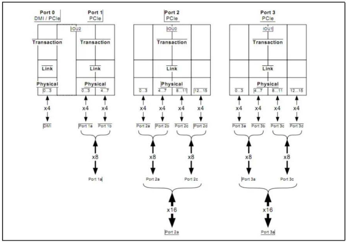
flowchart
graph TD
    subgraph Port 0
        A["Port 0 DMI / PCIe"] --> B["Transaction"]
        B --> C["Link"]
        C --> D["Physical 0...3"]
        D --> E["DMI"]
        F["Port 1 PCIe"] --> G["Transaction"]
        G --> H["Link"]
        H --> I["Physical 0...3"]
        I --> J["Port 1a"]
        K["x4"] --> L["DMI"]
        M["x4"] --> N["Port 1a"]
        O["x4"] --> P["Port 1b"]
        Q["x8"] --> R["Port 1a"]
        S["x4"] --> T["Port 1a"]
        U["x4"] --> V["Port 1b"]
    end

    subgraph Port 2
        W["Port 2 PCIe"] --> X["Transaction"]
        X --> Y["Link"]
        Y --> Z["Physical 0...3"]
        AA["x4"] --> AB["Port 2a"]
        AC["x4"] --> AD["Port 2b"]
        AE["x4"] --> AF["Port 2c"]
        AG["x4"] --> AH["Port 2d"]
        AI["x8"] --> AJ["Port 2a"]
        AK["x8"] --> AL["Port 2c"]
        AM["x8"] --> AN["Port 2d"]
        AO["x4"] --> AP["Port 3a"]
        AQ["x4"] --> AR["Port 3b"]
        AS["x4"] --> AT["Port 3c"]
        AU["x4"] --> AV["Port 3d"]
    end

    subgraph Port 3
        AW["Port 3 PCIe"] --> AX["Transaction"]
        AX --> AY["Link"]
        AZ["x8"] --> BA["Port 3a"]
        BB["x8"] --> BC["Port 3c"]
        BD["x16"] --> BE["Port 3a"]
        BF["x16"] --> BG["Port 3a"]
Figure 33. IIO PCI Express Lane Partitioning

Figure 34. Processor PCIe Link Speed Configuration Screen
Table 43. Setup Utility – Processor PCIe Link Speed Configuration Screen Fields
| Setup Item | Options | Help Text | Comments |
| Socket X PCIe Ports Link Speed | Configure PCIe ports link speed based on the processor. |
By entering the submenu screen will allow the user to configure PCIe port link speed in detail.
| Socket X PCIe Ports Link Speed | |
| Socket X, DMI | Gen2 (5GT/s) / Gen1 (2.5GT/s) |
| Socket X, PCIe Port 1a | Gen3 (8GT/s) / Gen2 (5GT/s) / Gen1 (2.5GT/s) |
| Socket X, PCIe Port 2a | Gen3 (8GT/s) / Gen2 (5GT/s) / Gen1 (2.5GT/s) |
| Socket X, PCIe Port 3a | Gen3 (8GT/s) / Gen2 (5GT/s) / Gen1 (2.5GT/s) |
| Socket X, PCIe Port 3c | Gen3 (8GT/s) / Gen2 (5GT/s) / Gen1 (2.5GT/s) |
Figure 35. Processor PCIe Link Speed Configuration in Detail
Table 44. Setup Utility – Processor PCIe Link Speed Configuration Screen Detail Fields
| Setup Item | Options | Help Text | Comments |
| Socket X, DMI | Gen2 (5GT/s)Gen1 (2.5GT/s) | DMI link speed selection. | |
| Socket X, PCIe Port xx | Gen3 (8GT/s)Gen2 (5GT/s)Gen1 (2.5GT/s) | PCIe Port link speed selection. |
5.4.2.15 Serial Port Configuration
The Serial Port Configuration screen allows the user to configure the Serial A [COM 1] and Serial B [COM2] ports.
To access this screen from the Main screen, select Advanced > Serial Port Configuration. To move to another screen, press the
| Advanced | |
| Serial Port Configuration | |
| Serial A Enable | Enabled / Disabled |
| Address | 3F8h / 2F8h / 3E8h / 2E8h |
| IRQ | 3 or 4 |
Figure 36. Serial Port Configuration Screen
Table 45. Setup Utility – Serial Ports Configuration Screen Fields
| Setup Item | Options | Help Text |
| Serial A Enable | EnabledDisabled | Enable or disable Serial port A. |
| Address | 3F8h2F8h3E8h2E8h | Select Serial port A base I/O address. |
| IRQ | 34 | Select Serial port A interrupt request (IRQ) line. |
5.4.2.16 USB Configuration
The USB Configuration screen allows the user to configure the USB controller options.
To access this screen from the Main screen, select Advanced > USB Configuration. To move to another screen, press the
| Advanced | |
| USB Configuration | |
| Detected USB Devices | |
| USB Controller | Enabled / Disabled |
| Legacy USB Support | Enabled / Disabled/Auto |
| Port 60/64 Emulation | Enabled / Disabled |
| Make USB Devices Non-Bootable | Enabled / Disabled |
| USB Mass Storage Device Configuration | |
| Device Reset timeout | 10 seconds / 20 seconds / 30 seconds / 40 seconds |
| Mass Storage Device: | |
| Auto / Floppy / Forced FDD / Hard Disk / CD-ROM | |
Figure 37. USB Configuration Screen
Table 46. Setup Utility – USB Configuration Screen Fields
| Setup Item | Options | Help Text | Comments |
| Detected USB Devices | Information only. Shows the number of USB devices in the system. | ||
| USB Controller | EnabledDisabled | [Enabled] – All on-board USB controllers are turned on and accessible by the OS.[Disabled] – All on-board USB controllers are turned off and inaccessible by the OS. | When Legacy USB Support is Disabled, USB devices are available only through OS drivers. |
| Legacy USB Support | EnabledDisabledAuto | USB device boot support and PS/2 emulation for USB keyboard and USB mouse devices.[Auto] – Legacy USB support is enabled if a USB device is attached. | Grayed out if the USB Controller is disabled. |
| Port 60/64 Emulation | EnabledDisabled | I/O port 60h/64h emulation support.Note: This may be needed for legacy USB keyboard support when using an OS that is USB unaware. | Grayed out if the USB Controller is disabled. |
| Make USB Devices Non-Bootable | EnabledDisabled | Exclude USB in Boot Table.[Enabled] – This removes all USB Mass Storage devices as Boot options.[Disabled] – This allows all USB Mass Storage devices as Boot options. | Grayed out if the USB Controller is disabled. |
| Device Reset timeout | 10 sec20 sec30 sec40 sec | USB Mass Storage device Start Unit command timeout.Setting to a larger value provides more time for a mass storage device to be ready, if needed. | Grayed out if the USB Controller is disabled. |
| Mass Storage Devices | AutoFloppyForced FDDHard DiskCD-ROM | [Auto] – USB devices less than 530 MB are emulated as floppies.[Forced FDD] – HDD formatted drive is emulated as an FDD (for example, ZIP drive). | This field is hidden if no USB Mass Storage devices are detected.This setup screen can show a maximum of eight USB Mass Storage devices on the screen. If more than eight devices are installed in the system, the “USB Devices Enabled” displays the correct count, but only the first eight devices discovered are displayed in this list. |
5.4.2.17 System Acoustic and Performance Configuration
The System Acoustic and Performance Configuration screen allows the user to configure the thermal control behavior of the system with respect to what parameters are used in the system's Fan Speed Control algorithms.
To access this screen from the Main screen, select Advanced > System Acoustic and Performance Configuration. To move to another screen, press the
| Advanced | |
| System Acoustic and Performance Configuration | |
| Set Throttling Mode Altitude | Auto / DCLTT / SCLTT / SOLTT 300m or less / 301m-900m / 901m - 1500m / Higher than 1500m |
| Set Fan Profile Fan PWM Offset | Performance / Acoustic 0 |
| Quiet Fan Idle Mode | Enabled / Disabled |
Figure 38. System Acoustic and Performance Configuration Screen
Table 47. Setup Utility – System Acoustic and Performance Configuration Screen Fields
| Setup Item | Options | Help Text | Comments |
| Set Throttling Mode | AutoDCLTTSCLTTSOLTT | [Auto] – Auto Throttling mode[DCLTT] – Dynamic Closed LoopThermal Throttling[SCLTT] – Static Closed LoopThermal Throttling[SOLTT] – Static Open LoopThermal Throttling | DCLTT is the expected mode for a board in an Intel chassis with inlet and outlet air temperature sensors and TSOD. The firmware can update the offset registers for closed loop during runtime, as the BIOS sends the dynamic CLTT offset temperature data.SCLTT is used with an OEM chassis and DIMMs with TSOD. The firmware does not change the offset registers for closed loop during runtime, although the Management Engine can do so.SOLTT is intended for a system with UDIMMs that do not have TSOD. The thermal control registers are configured during POST, and the firmware does not change them. |
| Altitude | 300m or less301m-900m901m-1500mHigher than 1500m | [300m or less] (980ft or less) –Optimal performance setting near sea level[301m-900m] (980ft-2950ft) –Optimal performance setting at moderate elevation[901m-1500m] (2950ft-4920ft) –Optimal performance setting at high elevation[Higher than 1500m] (4920ft or greater) – Optimal performance setting at the highest elevations | This option sets an altitude value in order to choose a Fan Profile that is optimized for the air density at the current altitude at which the system is installed. |
| Set Fan Profile | Performance Acoustic | [Performance] – Fan control provides primary system cooling before attempting to throttle memory.[Acoustic] – The system will favor using throttling of memory over boosting fans to cool the system if thermal thresholds are met. | This option allows the user to choose a Fan Profile that is optimized for maximizing performance or for minimizing acoustic noise.When Performance is selected, the thermal conditions in the system are controlled by raising fan speed when necessary to raise cooling performance. This provides cooling without impacting system performance, but may impact system acoustic performance – fans running faster are typically louder.When Acoustic is selected, rather than increasing fan speed for additional cooling, the system will attempt first to control thermal conditions by throttling memory to reduce heat production.This regulates the system's thermal condition without changing the acoustic performance, but throttling memory may impact system performance. |
| Fan PWM Offset | [Entry Filed] | Valid Offset 0-100. This number is added to the calculated PWM value to increase Fan Speed. | This is a percentage by which the calculated fan speed will be increased.The user can apply positive offsets that result in increasing the minimum fan speeds. |
| Quiet Fan Idle Mode | Enabled Disabled | Enabling this option allows the system fans to operate in Quiet “Fan off” mode while still maintaining sufficient system cooling. In this mode, fan sensors become unavailable and cannot be monitored. There will be limited fan related event generation. | When enabled, this option allows fans to idle or turn off when sufficient thermal margin is available, decreasing the acoustic noise produced by the system and decreasing system power consumption. Fans will run as needed to maintain thermal control. The actual decrease in fan speed depends on the system thermal loading, which in turn depends on system configuration and workload.While Quiet Fan Idle Mode is engaged, fan sensors become unavailable and are not monitored by the BMC. |
5.4.2.18 Security Screen (Tab)
The Security screen allows the user to enable and set the user and administrative password and to lock out the front panel buttons so they cannot be used. This screen also allows the user to enable and activate the Trusted Platform Module (TPM) security settings on those boards that support TPM.
To access this screen from the Main screen or other top-level Tab screen, press the right or left arrow key to traverse the tabs at the top of the Setup screen until the Security screen is selected.
| Main | Advanced | Security | Server Management | Boot Options | Boot Manager |
| Administrator Password Status | |||||
| User Password | |||||
| Set Administrator Password | |||||
| Set User Password | [123aBcD] | ||||
| Power ON Password | Enabled / Disabled | ||||
| Front Panel Lockout | Enabled / Disabled | ||||
Figure 39. Security Screen
Table 48. Setup Utility – Security Screen Fields
| Setup Item | Options | Help Text | Comments |
| Administrator Password Status | InstalledNot Installed | Information only. Indicates the status of the administrator password. | |
| User Password Status | InstalledNot Installed | Information only. Indicates the status of the user password. | |
| Set Administrator Password | [Entry Field] | Administrator password is used to control change access to BIOS Setup Utility.Only alphanumeric characters can be used. Maximum length is seven characters. It is case sensitive.Note: Administrator password must be set in order to use the user account. | This option is only to control access to the setup. Administrator has full access to all the setup items.Clearing the Administrator password also clears the user password. |
| Set User Password | [Entry Filed] | User password is used to control entry access to BIOS Setup Utility. Only alphanumeric characters can be used. Maximum length is 7 characters. It is case sensitive.Note: Removing the administrator password also automatically removes the user password. | Available only if the administrator password is installed. This option only protects the setup.User password only has limited access to the setup items. |
| Power ON Password | EnabledDisabled | Enable Power On Password support. If enabled, password entry is required in order to boot the system. | When Power On Password security is enabled, the system will halt soon after power-on and the BIOS will ask for a password before continuing POST and booting. Either the Administrator or User password may be used.If an Administrator password has not been set, this option will be grayed out and unavailable. If this option is enabled and the Administrator password is removed, this will also disable this option. |
| Front Panel Lockout | EnabledDisabled | If enabled, locks the power button OFF function and the reset and NMI Diagnostic Interrupt buttons on the system's front panel. If [Enabled] is selected, power-off and reset must be controlled via a system management interface, and the NMI Diagnostic Interrupt is not available. |
5.4.2.19 Server Management Screen (Tab)
The Server Management screen allows the user to configure several server management features. This screen also provides an access point to the screens for configuring console redirection, displaying system information, and controlling the BMC LAN configuration.
To access this screen from the Main screen or other top-level Tab screen, press the right or left arrow key to traverse the tabs at the top of the Setup screen until the Server Management screen is selected.
| Main | Advanced | Security | Server Management | Boot Options | Boot Manager |
| Assert NMI on SERR | Enabled / Disabled | ||||
| Assert NMI on PERR | Enabled / Disabled | ||||
| PCIe AER Support | Enabled / Disabled | ||||
| Log Correctable Errors | Enabled / Disabled | ||||
| Reset on CATERR | Enabled / Disabled | ||||
| Reset on ERR2 | Enabled / Disabled | ||||
| Resume on AC Power Loss | Stay Off / Last state / Power On | ||||
| Power Restore Delay | Disabled / Auto / Fixed | ||||
| Power Restore Delay Value | 25 | ||||
| Clear System Event Log | Enabled / Disabled | ||||
| FRB-2 Enable | Enabled / Disabled | ||||
| OS Boot Watchdog Timer | Enabled / Disabled | ||||
| OS Boot Watchdog Timer Policy | Power off / Reset | ||||
| OS Boot Watchdog Timer Timeout | 5 minutes / 10 minutes / 15 minutes / 20 minutes | ||||
| Plug and Play BMC Detection | Enabled / Disabled | ||||
| Shutdown Policy | Enabled / Disabled | ||||
| ► Console Redirection | |||||
| ► System Information | |||||
| ► BMC LAN Configuration | |||||
Figure 40. Server Management Screen
Table 49. Setup Utility – Server Management Screen Fields
| Setup Item | Options | Help Text | Comments |
| Assert NMI on SERR | EnabledDisabled | On SERR, generate an NMI and log an error.Note: [Enabled] must be selected for the Assert NMI on PERR setup option to be visible. | |
| Assert NMI on PERR | EnabledDisabled | On PERR, generate an NMI and log an error.Note: This option is active only if the Assert NMI on SERR option is [Enabled] selected. | |
| PCIe AER Support | EnabledDisabled | Enable or Disable PCIe AER(Advanced Error Reporting). | PCIe AER error will be masked after PCIe AER is disabled. |
| Log Correctable Errors | EnabledDisabled | ||
| Reset on CATERR | EnabledDisabled | When enabled system gets reset upon encountering Catastrophic Error (CATERR); when disabled system does not get reset on CATERR. | This option controls whether the system will be reset when the CATERR signal is held asserted, rather than just pulsed to generate an SMI. |
| Reset on ERR2 | EnabledDisabled | When enabled system gets reset upon encountering ERR2 (Fatal error); when disabled system does not get reset on ERR2. | This option controls whether the system will be reset if the BMC's ERR2 Monitor times out, that is, the ERR2 signal has been continuously asserted long enough to indicate that the SMI Handler is not able to service the condition. |
| Resume on AC Power Loss | Stay OffLast state Reset | System action to take on AC power loss recovery.[Stay Off] - System stays off.[Last State] - System returns to the same state before the AC power loss.[Reset] - System powers on. | |
| Clear System Event Log | EnabledDisabled | If enabled, clears the System Event Log. All current entries will be lost.Note: This option is reset to [Disabled] after a reboot. | |
| FRB-2 Enable | EnabledDisabled | Fault Resilient Boot (FRB).If enabled, the BIOS programs the BMC watchdog timer for approximately six minutes. If the BIOS does not complete POST before the timer expires, the BMC resets the system. | |
| O/S Boot Watchdog Timer | EnabledDisabled | If enabled, the BIOS programs the watchdog timer with the timeout value selected. If the OS does not complete booting before the timer expires, the BMC resets the system and an error is logged.Requires OS support or Intel® Management Software. | |
| O/S Boot Watchdog Timer Policy | Power OffReset | If the OS boot watchdog timer is enabled, this is the system action taken if the watchdog timer expires.[Reset] - System performs a reset.[Power Off] - System powers off. | Grayed out when the O/S Boot Watchdog Timer is disabled. |
| O/S Boot Watchdog Timer Timeout | 5 minutes10 minutes15 minutes20 minutes | If the OS watchdog timer is enabled, this is the timeout value used by the BIOS to configure the watchdog timer. | Grayed out when the O/S Boot Watchdog Timer is disabled. |
| Plug and Play BMC Detection | Enabled Disabled | If enabled, the BMC is detectable by OSes that support plug and play loading of an IPMI driver. Do not enable if your OS does not support this driver. | |
| Shutdown Policy | Enabled Disabled | Enable/Disable Shutdown Policy. | This option is designed for multiple-node systems and to control the policy that the BMC should shut down one node if it detected over-current or over-temperature condition. The BIOS and the BMC will synchronize the policy during the BIOS POST and current value of the BMC will be displayed in BIOS Setup.This option only shows on Node 3 and Node 4. |
| Console Redirection | View/Configure console redirection information and settings. | Takes the user to the Console Redirection screen. | |
| System Information | View system information. | Takes the user to the System Information screen. | |
| BMC LAN Configuration | View/Configure BMC LAN channel and user settings. | Takes the user to the BMC configuration screen. |
5.4.2.20 Console Redirection
The Console Redirection screen allows the user to enable or disable Console Redirection for Remote Management, and to configure the connection options for this feature.
To access this screen from the Main screen, select Server Management > Console Redirection. To move to another screen, press the
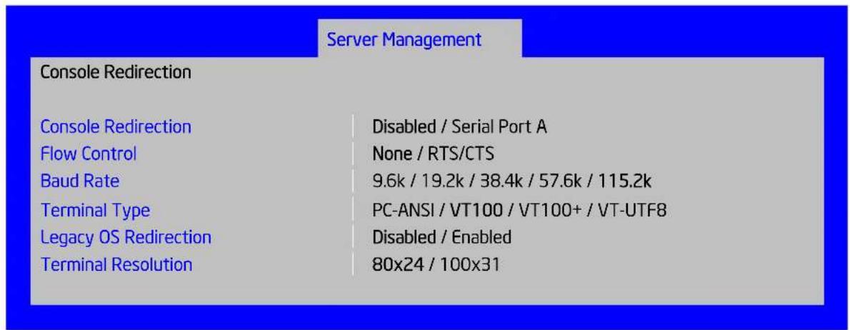
Figure 41. Console Redirection Screen
Table 50. Setup Utility – Console Redirection Screen Fields
| Setup Item | Options | Help Text |
| Console Redirection | DisabledSerial Port A | Console redirection allows a serial port to be used for server management tasks.[Disabled] – No console redirection.[Serial Port A] – Configure serial port A for console redirection.Enabling this option disables the display of the Quiet Boot logo screen during POST. |
| Flow Control | NoneRTS/CTS | Flow control is the handshake protocol.Setting must match the remote terminal application.[None] – Configure for no flow control.[RTS/CTS] – Configure for hardware flow control. |
| Baud Rate | 960019.2K38.4K57.6K115.2K | Serial port transmission speed. Setting must match the remote terminal application. |
| Terminal Type | PC-ANSIVT100VT100+VT-UTF8 | Character formatting used for console redirection. Setting must match the remote terminal application. |
| Legacy OS Redirection | DisabledEnabled | This option enables legacy OS redirection (that is, DOS) on serial port. If it is enabled, the associated serial port is hidden from the legacy OS. |
| Terminal Resolution | 80x24100x31 | Terminal screen resolution for console redirection. |
5.4.2.21 System Information
The System Information screen allows the user to view part numbers, serial numbers, and firmware revisions. This is an Information Only screen.
To access this screen from the Main screen, select Server Management > System Information. To move to another screen, press the
| Server Management | |
| System Information | |
| Board Part Number | <Part Number display> |
| Board Serial Number | <Serial Number display> |
| System Part Number | <Part Number display> |
| System Serial Number | <Serial Number display> |
| Chassis Part Number | <Part Number display> |
| Chassis Serial Number | <Serial Number display> |
| Asset Tag | <Asset Tag-display> |
| BMC Firmware Revision | <BMC FW Rev display> |
| HSC Firmware Revision | <HSC FW Rev display> |
| ME Firmware Revision | <ME FW Rev display> |
| SDR Revision | <SDR Rev display> |
| UUID | <UUID display> |
Figure 42. System Information Screen
Table 51. Setup Utility – System Information Screen Fields
| Setup Item | Help Text | Comments |
| Board Part Number | Information only. | |
| Board Serial Number | Information only. | |
| System Part Number | Information only. | |
| System Serial Number | Pressto edit system Serial Number and then use Backspace to delete existing value.Maximum length is 20 characters. | Information only. |
| Chassis Part Number | Information only. | |
| Chassis Serial Number | Information only. | |
| Asset Tag | Pressto edit system Serial Number and then use Backspace to delete existing value.Maximum length is 20 characters. | Information only. |
| BMC Firmware Revision | Information only. | |
| HSC Firmware Revision | Information only. If there is no HSC installed, the Firmware Revision Number appears as “0,00”. | |
| ME Firmware Revision | Information only. | |
| SDR Revision | Information only. | |
| UUID | Information only. |
5.4.2.22 BMC LAN Configuration
The BMC LAN Configuration screen allows the Setup user to configure the BMC Baseboard LAN channel and the RMM4 LAN channel, and to manage BMC User settings for up to five BMC Users.
To access this screen from the Main screen, select Server Management > System Information. To move to another screen, press the
Server Management
| BMC LAN Configuration | |
| Baseboard LAN configuration | |
| IP Source | Static/Dynamic |
| IP Address | [0.0.0.0 IP display/edit] |
| Subnet Mask | [0.0.0.0 IP display/edit] |
| Gateway IP | [0.0.0.0 IP display/edit] |
| Baseboard LAN IPV6 configuration | |
| IPV6 | Disable/Enable |
| IPV6 source | Static/Dynamic/Auto |
| IPV6 address | 0000:0000:0000:0000 |
| Gateway IPV6 | 0000:0000:0000:0000 |
| IPV6 Prefix Length | 64 |
| Intel® RMM4 IPV4 LAN configuration | |
| Intel® RMM4 | |
| IP Source | Static/Dynamic |
| IP Address | [0.0.0.0 IP display/edit] |
| Subnet Mask | [0.0.0.0 IP display/edit] |
| Gateway IP | [0.0.0.0 IP display/edit] |
| Intel® RMM4 IPV6 LAN configuration | |
| Intel® RMM4 | |
| IPV6 Source | Static/Dynamic |
| IPV6 Address | 0000:0000:0000:0000 |
| Gateway IPV6 | 0000:0000:0000:0000 |
| IPV6 Prefix Length | 64 |
| BMC DHCP Host Name | [DHCP Host Name display/edit] |
| User Configuration | |
| User ID | anonymous/root/User3/User4/User5 |
| Privilege | Callback/ User/Operator/Administrator |
| User status | Disable/Enable |
| User Name | [User Name display/edit] |
| User Password. | |
Figure 43. BMC LAN Configuration Screen
Table 52. Setup Utility – BMC LAN Configuration Screen Fields
| Setup Item | Options | Help Text | Comments |
| IP source | Static Dynamic | Select BMC IP source. When Static option is selected, IP address, subnet mask, and gateway are editable. When Dynamic option selected, these fields are read-only and IP is address acquired automatically (DHCP). | |
| IP address | View/edit IP address. Pressto edit. | ||
| Subnet Mask | View/edit subnet address. Pressto edit. | ||
| Gateway IP | View/edit Gateway IP address. Pressto edit. | ||
| Intel® RMM4 | Present Not Present | Information only. | |
| IP source | Static Dynamic | Select BMC IP source. When Static option is selected, IP address, subnet mask, and gateway are editable. When Dynamic option selected, these fields are read-only and IP is address acquired automatically (DHCP). | |
| IP address | View/edit IP address. Pressto edit. | ||
| Subnet Mask | View/edit subnet address. Pressto edit. | ||
| Gateway IP | View/edit Gateway IP address.Pressto edit. | ||
| BMC DHCP Host Name | View/edit BMC DHCP host name. Pressto edit. | Available only when IP source for any one channel is dynamic option. | |
| User ID | anonymous root User3 User4 User5 | Select the user id to configure. | |
| Privilege | Callback User Operator Administrator | View/select user privilege. | |
| User Status | Enable Disable | Enable/disable LAN access for selected user. Also enables/disables SOL, KVM media redirection. | |
| User Name | Pressto edit user name. The user name is a string of 4 to 15 alphanumeric characters. The user name must begin with an alphabetic character. | ||
| User Password | PressKey to enter password. Only alphanumeric characters can be used. Maximum length is 15 characters and case sensitive.Note:Password entered will override any previously set password. | This filed will not indicate whether there is password set already. |
5.4.2.23 Boot Options Screen (Tab)
The Boot Options screen displays all bootable media encountered during POST, and allows the user to configure the desired order in which boot devices are to be tried.
The first boot device in the specified Boot Order that is present and is bootable during POST will be used to boot the system, and will continue to be used to reboot the system until the boot device configuration has changed (that is, which boot devices are present), or until the system has been powered down and booted in a cold power-on boot.
If all types of bootable devices are installed in the system, the default boot order is as follows:
- CD/DVD-ROM
- Floppy Disk Drive
- Hard Disk Drive
- PXE Network Device
■ BEV (Boot Entry Vector) Device
■ EFI Shell and EFI Boot paths
To access this screen from the Main screen or other top-level Tab screen, press the right or left arrow key to traverse the tabs at the top of the Setup screen until the Boot Options screen is selected.
| Main Advanced Security Server Management Boot Options Boot Manager | ||||
| System Boot Timeout <0 - 65535, 0 is default> | ||||
| Boot Option #1 | ||||
| Boot Option #2 | ||||
| Boot Option #n | ||||
| ► CDROM Order | ||||
| ► Hard Disk Order | ||||
| ► Floppy Order | ||||
| ► Network Device Order | ||||
| ► BEV Device Order | ||||
| ► Add EFI Boot Option | ||||
| ► Delete EFI Boot Option | ||||
| EFI Optimized Boot Enabled/Disabled | ||||
| Boot Option Retry Enabled/Disabled | ||||
| USB Boot Priority Enabled/Disabled | ||||
| Static Boot Ordering Enabled/Disabled | ||||
| Reset Static Boot Order Yes/No Action | ||||
Figure 44. Boot Options Screen
Table 53. Boot Options Screen Fields
| Setup Item | Options | Help Text | Comments |
| Boot Timeout | 0-65535 | The number of seconds the BIOS should pause at the end of POST to allow the user to press the [F2] key for entering the BIOS Setup utility. Valid values are 0-65535. Zero is the default. A value of 65535 causes the system to go to the Boot Manager menu and wait for user input for every system boot. | After entering the necessary timeout, press the Enter key to register that timeout value to the system. These settings are in seconds. |
| Boot Option #x | Available boot devices. | Set system boot order by selecting the boot option for this position. | |
| CDROM Oder | Set the order of the Legacy devices in this group. | Selection only. | |
| Hard Disk Order | Set the order of the Legacy devices in this group. | Displays when one or more hard disk drives are in the system. | |
| Floppy Order | Set the order of the Legacy devices in this group. | Selection only. | |
| Network Device Order | Set the order of the Legacy devices in this group. | Displays when one or more of these devices are available in the system. | |
| BEV Device Order | Set the order of the Legacy devices in this group. | Selection only. | |
| EFI Optimized Boot | Enabled Disabled | If enabled, the BIOS only loads modules required for booting EFI-aware Operating Systems. | Grayed out when [SW RAID] SATA Mode is Enabled. SW RAID can only be used in Legacy Boot mode. |
| Boot Option Retry | Enabled Disabled | If enabled, this continually retries non-EFI-based boot options without waiting for user input. | |
| USB Boot Priority | Enabled Disabled | If enabled, newly discovered USB devices will be put to the top of their boot device category. If disabled, newly discovered USB devices will be put at the bottom of the respective list. | |
| Static Boot Ordering | Enabled Disabled | [Disabled] – Devices removed from the system are deleted from Boot Order Tables. [Enabled] – Devices removed have positions in Boot Order Tables retained for later reinsertion. | When the option changes to “Enabled” from “Disabled”, it will enable Static Boot Ordering (SBO) from the next boot onward, and also the current Boot Order will be stored as the SBO template. When the option changes to “Disabled” from “Enabled”, it will disable SBO and the SBO template will be cleared. Otherwise it will retain the current Enabled/Disabled state. |
| Reset Static Boot Order | YesNo Action | [Yes] – Take snapshot of current boot order to save as Static Boot Order Template. | This option allows you to take the current Boot Options and save it as the Static Boot Option template without disabling and re-enabling the Static Boot Ordering option.Select “Yes” to snapshot the current Boot Options into the Static Boot Options. After saving SBO, on next boot this option will change back to “No Action” automatically. |
5.4.2.24 CDROM Order
The CDROM Order screen allows the user to control the order in which BIOS attempts to boot from the optical drives installed in the system. This screen is available only when there is at least one optical device available in the system configuration. Note that a USB attached CDROM drive or a USB Key device formatted as a CDROM will appear in this section.
To access this screen from the Main screen, select Boot Options > CDROM Order. To move to another screen, press the
| Boot Options | |
| Hard Disk Order | |
| CDROM #1 | <Available Hard Disk devices> |
| CDROM #2 | <Available Hard Disk devices> |
Figure 45. CDROM Order Screen
Table 54. Boot Option – CDROM Order Screen Fields
| Setup Item | Options | Help Text |
| CDROM #1 | Available Legacy devices for this Device group. | Set system boot order by selecting the boot option for this position. |
| CDROM #2 | Available Legacy devices for this Device group. | Set system boot order by selecting the boot option for this position. |
5.4.2.25 Hard Disk Order
The Hard Disk Order screen allows the user to control the order in which BIOS attempts to boot from the hard disk drives installed in the system. This screen is available only when there is at least one hard disk device available in the system configuration. Note that a USB attached Hard Disk drive or a USB Key device formatted as a hard disk will appear in this section.
To access this screen from the Main screen, select Boot Options > Hard Disk Order. To move to another screen, press the
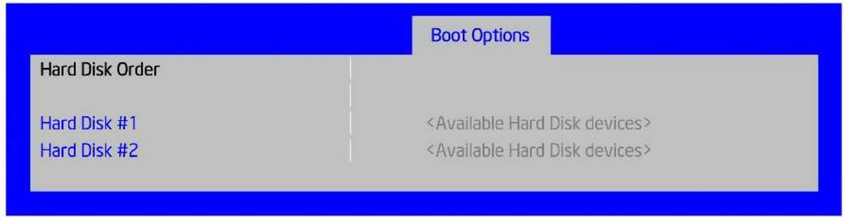
Figure 46. Hard Disk Order Screen
Table 55. Boot Option – Hard Disk Order Screen Fields
| Setup Item | Options | Help Text |
| Hard Disk #1 | Available Legacy devices for this Device group. | Set system boot order by selecting the boot option for this position. |
| Hard Disk #2 | Available Legacy devices for this Device group. | Set system boot order by selecting the boot option for this position. |
5.4.2.26 Floppy Order
The Floppy Order screen allows the user to control the order in which BIOS attempts to boot from the floppy drives installed in the system. This screen is available only when there is at least one floppy device available in the system configuration. Note that a USB attached floppy drive or a USB Key device formatted as a floppy will appear in this section.
To access this screen from the Main screen, select Boot Options > Floppy Order. To move to another screen, press the
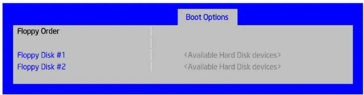
Figure 47. Floppy Order Screen
Table 56. Boot Option – Floppy Order Screen Fields
| Setup Item | Options | Help Text |
| Floppy Disk #1 | Available Legacy devices for this Device group. | Set system boot order by selecting the boot option for this position. |
| Floppy Disk #2 | Available Legacy devices for this Device group. | Set system boot order by selecting the boot option for this position. |
5.4.2.27 Network Device Order
The Network Device Order screen allows the user to control the order in which BIOS attempts to boot from the network bootable devices installed in the system. This screen is available only when there is at least one network bootable device available in the system configuration.
To access this screen from the Main screen, select Boot Options > Network Device Order. To move to another screen, press the
| Boot Options | |
| Network Device Order | |
| Network Device #1 | |
| Network Device #2 |
Figure 48. Network Device Order Screen
Table 57. Boot Option – Network Device Order Screen Fields
| Setup Item | Options | Help Text |
| Network Device #1 | Available Legacy devices for this Device group. | Set system boot order by selecting the boot option for this position. |
| Network Device #2 | Available Legacy devices for this Device group. | Set system boot order by selecting the boot option for this position. |
5.4.2.28 BEV Device Order
The BEV Device Order screen allows the user to control the order in which BIOS attempts to boot from the BEV drives installed in the system. This screen is available only when there is at least one BEV device available in the system configuration.
To access this screen from the Main screen, select Boot Options > BEV Device Order. To move to another screen, press the
Boot Options
BEV Device Order
BEV Device #1
BEV Device #2
Figure 49. BEV Device Order Screen
Table 58. Boot Option – BEV Device Order Screen Fields
| Setup Item | Options | Help Text |
| BEV Device #1 | Available Legacy devices for this Device group. | Set system boot order by selecting the boot option for this position. |
| BEV Device #2 | Available Legacy devices for this Device group. | Set system boot order by selecting the boot option for this position. |
5.4.2.29 Add EFI Boot Option
The Add EFI Boot Option screen allows the user to add an EFI boot option to the boot order. This screen is available only when there is at least one EFI bootable device present in the system configuration. The “Internal EFI Shell” Boot Option is permanent and cannot be added or deleted.
To access this screen from the Main screen, select Boot Options > Add EFI Boot Option. To move to another screen, press the
Boot Options
Add EFI Boot Option
Add Boot Option Label
[Enter label]
Select File System
Path for Boot Option
[Enter Boot Path]
Save
Figure 50. Add EFI Boot Option Screen
Table 59. Boot Option – Add EFI Boot Option Screen Fields
| Setup Item | Options | Help Text | Comments |
| Add Boot Option Label | [Enter Label] | Create the label for new boot option. | This label becomes an abbreviation for this Boot Path. |
| Select File System | Available File System | Select the file system from the list. | Choose the file system on which this boot path resides. |
| Path for Boot Option | [Enter Boot Path] | Enter the path to the boot option in the format \path\filename.efi. | This will be the Boot Path, residing on the file system chosen, which will enter into the Boot Order with the Label entered above. |
| Save | Save the boot option. | Selection only. This will save the new Boot Option into the Boot Order. |
5.4.2.30 Delete EFI Boot Option
The Delete EFI Boot Option screen allows the user to remove an EFI boot option from the boot order. The “Internal EFI Shell” Boot Option will not be listed, since it is permanent and cannot be added or deleted.
To access this screen from the Main screen, select Boot Options > Delete EFI Boot Option. To move to another screen, press the
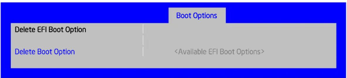
flowchart
graph TD
    A["Boot Options"] --> B["Delete EFI Boot Option"]
    A --> C["Delete Boot Option"]
    C --> D["<Available EFI Boot Options>"]
Figure 51. Delete EFI Boot Option Screen
Table 60. Boot Option – Delete EFI Boot Option Screen Fields
| Setup Item | Options | Help Text | Comments |
| Delete Boot Option | Select one to delete. | This will not allow a user to delete the EFI Shell. |
5.4.2.31 Boot Manager Screen (Tab)
The Boot Manager screen allows the user to view a list of devices available for booting, and to select a boot device for immediately booting the system. Note that this list is not in order according to the system Boot Option order. The Internal EFI Shell will always be available, regardless of whether any other bootable devices are available.
To access this screen from the Main screen or other top-level Tab screen, press the right or left arrow key to traverse the tabs at the top of the Setup screen until the Boot Manager screen is selected.
| Main | Advanced | Security | Server Management | Boot Options | Boot Manager |
| Launch EFI Shell | |||||
| <Boot device #1> | |||||
| <Boot Option #2> | |||||
| <Boot Option #n> |
Figure 52. Boot Manager Screen
Table 61. Setup Utility – Boot Manager Screen Fields
| Setup Item | Value | Help Text | Comment |
| Launch EFI Shell | Select this option to boot now.Note: This list is not the system boot option order. Use the Boot Options menu to view and configure the system boot option order. | This will not allow a user to delete the EFI Shell. | |
| Boot Device #n | Select this option to boot now.Note: This list is not the system boot option order. Use the Boot Options menu to view and configure the system boot option order. | These are names of bootable devices discovered in the system. The system user can choose any of them from which to initiate a one-time boot – that is, booting from any device in this list will not permanently affect the defined system Boot Order.These bootable devices are not displayed in any specified order, particularly not in the system Boot Order established by the Boot Options screen. This is just a list of bootable devices in the order in which they were enumerated. |
5.4.2.32 Error Manager Screen (Tab)
The Error Manager screen displays any POST Error Codes encountered during BIOS POST, along with an explanation of the meaning of the Error Code in the form of a Help Text. This is an Information Only screen.
To access this screen from the Main screen or other top-level Tab screen, press the right or left arrow key to traverse the tabs at the top of the Setup screen until the Error Manager screen is selected.
| Error Manager | Save&Exit | ||
| View Event Log | |||
| ERROR CODE | SEVERITY | INSTANCE | |
| 5224 | Major | N/A | This is an example. |
Figure 53. Error Manager Screen
Table 62. Setup Utility – Error Manager Screen Fields
| Setup Item | Options | Help Text | Comments |
| Displays System Errors | Information only. Displays errors that occurred during POST. |
5.4.2.33 Save and Exit Screen (Tab)
The Save & Exit screen allows the user to choose whether to save or discard the configuration changes made on other Setup screens. It also allows the user to restore the BIOS settings to the factory defaults or to save or restore them to a set of user-defined default values. If Load Default Values is selected, the factory default settings (noted in bold in the Setup screen images) are applied. If Load User Default Values is selected, the system is restored to the previously saved user-defined default values.
To access this screen from the Main screen or other top-level Tab screen, press the right or left arrow key to traverse the tabs at the top of the Setup screen until the Save & Exit screen is selected.
| Error Manager | Save & Exit |
| Save Changes and Exit | |
| Discard Changes and Exit | |
| Save Changes | |
| Discard Changes | |
| Load Default Values | |
| Save as User Default Values | |
| Load User Default Values | |
Figure 54. Save & Exit Screen
Table 63. Setup Utility – Save & Exit Screen Fields
| Setup Item | Help Text | Comments |
| Save Changes and Exit | Exit the BIOS Setup utility after saving changes. The system reboots if required.The [F10] key can also be used. | User prompted for confirmation only if any of the setup fields were modified. |
| Discard Changes and Exit | Exit the BIOS Setup utility without saving changes.The [Esc] key can also be used. | User prompted for confirmation only if any of the setup fields were modified. |
| Save Changes | Save changes without exiting the BIOS Setup Utility.Note: Saved changes may require a system reboot before taking effect. | User prompted for confirmation only if any of the setup fields were modified. |
| Discard Changes | Discard changes made since the last Save Changes operation was performed. | User prompted for confirmation only if any of the setup fields were modified. |
| Load Default Values | Load factory default values for all BIOS Setup utility options.The [F9] key can also be used. | User prompted for confirmation. |
| Save as User Default Values | Save current BIOS Setup utility values as custom user default values. If needed, the user default values can be restored through the Load User Default Values option given as follows.Note: Clearing the CMOS or NVRAM does not cause the User Default values to be reset to the factory default values. | User prompted for confirmation. |
| Load User Default Values | Load user default values. | User prompted for confirmation. |
5.5 Loading BIOS Defaults
Different mechanisms exist for resetting the system configuration to the default values. When a request to reset the system configuration is detected, the BIOS loads the default system configuration values during the next POST. You can send the request to reset the system to the defaults in the following ways:
- Pressing
from within the BIOS Setup utility. - Moving the clear system configuration jumper.
- IPMI command (set System Boot options command).
- Int15 AX=DA209.
- Choosing Load User Defaults from the Save & Exit page of the BIOS Setup loads user set defaults instead of the BIOS factory defaults.
The recommended steps to load the BIOS defaults are:
- Power down the system (Do not remove AC power).
- Move the BIOS DFLT jumper from pins 1-2 to pins 2-3.
- Move the BIOS DFLT jumper from pins 2-3 to pins 1-2.
- Power up the system.
6. Configuration Jumpers
The following table provides a summary and description of configuration, test, and debug jumpers on the Intel ^® Server Board S2600JF. The server board has several 3-pin jumper blocks that can be used.
Pin 1 on each jumper block can be identified by the following symbol on the silkscreen.
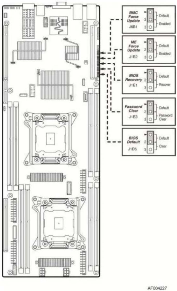
Figure 55. Jumper Blocks (J6B1, J1E2, J1E3, J1E1, and J1D5)
Table 64. Server Board Jumpers (J6B1, J1E2, J1E3, J1E1, and J1D5)
| Jumper Name | Jumper Position | Mode of Operation | Note |
| J6B1: BMC Force Update jumper | 1-2 | Normal | Normal mode |
| 2-3 | Update | BMC in force update mode | |
| J1E2: ME Force Update | 1-2 | Normal | Normal mode |
| 2-3 | Update | ME in force update mode | |
| J1E3: Password Clear | 1-2 | Normal | Normal mode, password in protection |
| 2-3 | Clear Password | BIOS password is cleared | |
| J1E1: BIOS Recovery Mode | 1-2 | Normal | Normal mode |
| 2-3 | Recovery | BIOS in recovery mode | |
| J1D5: BIOS Default | 1-2 | Normal | Normal mode |
| 2-3 | Clear BIOS Settings | BIOS settings are reset to factory default |
6.1 Force Integrated BMC Update (J6B1)
When performing a standard BMC firmware update procedure, the update utility places the BMC into an update mode, allowing the firmware to load safely onto the flash device. In the unlikely event the BMC firmware update process fails due to the BMC not being in the proper update state, the server board provides a BMC Force Update jumper (J6B1) that will force the BMC into the proper update state. The following procedure should be followed in the event the standard BMC firmware update process fails.
Table 65. Force Integrated BMC Update Jumper
| Jumper Position | Mode of Operation | Note |
| 1-2 | Normal | Normal operation |
| 2-3 | Update | BMC in force update mode |
Steps to perform Force BMC Update:
- Remove the compute module from the chassis when the compute node is powered down.
- Remove the air duct from the compute module.
- Move jumper from the default operating position (covering pins1 and 2) to the enabled position (covering pins 2 and 3).
- Restore the air duct to the compute module.
- Plug in the compute module back to the chassis.
- Perform the BMC firmware update procedure as documented in the ReleaseNote.TXT file included in the given BMC firmware update package. After successful completion of the firmware update process, the firmware update utility may generate an error stating the BMC is still in update mode.
- Power down the compute module and remove it from the chassis.
- Remove the air duct from the compute module.
- Move the jumper from the enabled position (covering pins 2 and 3) to the disabled position (covering pins 1 and 2).
-
Restore the air duct.
-
Plug in the compute module back to the chassis.
Note: Normal BMC functionality is disabled with the Force BMC Update jumper set to the enabled position. You should never run the server with the BMC Force Update jumper set in this position. You should only use this jumper setting when the standard firmware update process fails. This jumper should remain in the default/disabled position when the server is running normally.
The server board has several 3-pin jumper blocks that can be used to configure, protect, or recover specific features of the server board.
6.2 Force ME Update (J1E2)
When this 3-pin jumper is set, it manually puts the ME firmware in update mode, which enables the user to update ME firmware code when necessary.
Table 66. Force ME Update Jumper
| Jumper Position | Mode of Operation | Note |
| 1-2 | Normal | Normal operation |
| 2-3 | Update | ME in force update mode |
Note: Normal ME functionality is disabled with the Force ME Update jumper set to the enabled position. You should never run the server with the ME Force Update jumper set in this position. You should only use this jumper setting when the standard firmware update process fails. This jumper should remain in the default/disabled position when the server is running normally.
Steps to perform the Force ME Update:
- Remove the compute module from the chassis when the module is powered down.
- Remove the air duct from the compute module.
- Move jumper from the default operating position (covering pins 1 and 2) to the enabled position (covering pins 2 and 3).
- Restore the air duct and plug in the module to the chassis.
- Power up the compute module.
- Perform the ME firmware update procedure as documented in the README.TXT file that is included in the given ME firmware update package (same package as BIOS).
- Power down the compute module and remove it from the chassis.
- Remove the air duct from the compute module.
- Move jumper from the enabled position (covering pins 2 and 3) to the disabled position (covering pins 1 and 2).
- Restore the air duct and plug in the compute module to the chassis.
6.3 Password Clear (J1B6)
The user sets this 3-pin jumper to clear the password.
Table 67. Password Clear Jumper
| Jumper Position | Mode of Operation | Note |
| 1-2 | Normal | Normal mode, password in protection |
| 2-3 | Clear Password | BIOS password is cleared |
Steps to clear the BIOS password:
- Plug out the compute module from chassis.
- Remove the air duct.
- Move jumper (J1B6) from the default operating position (covering pins 1 and 2) to the password clear position (covering pins 2 and 3).
- Plug in compute module in chassis and power on for 10 seconds or until POST completes.
- Plug out the compute module.
- Move the jumper back to default position (covering pins 1 and 2).
- Restore the air duct.
- Plug in compute module back to chassis.
- Power up the compute module.
The password is now cleared and you can reset it by going into the BIOS setup.
6.4 BIOS Recovery Mode (J1E1)
The Intel ^® Server Board S2600JF uses BIOS recovery to repair the system BIOS from flash corruption in the main BIOS and Boot Block. This 3-pin jumper is used to reload the BIOS when the image is suspected to be corrupted. For directions on how to recover the BIOS, refer to the specific BIOS release notes.
Table 68. BIOS Recovery Mode Jumper
| Jumper Position | Mode of Operation | Note |
| 1-2 | Normal | Normal mode |
| 2-3 | Recovery | BIOS in recovery mode |
You can accomplish a BIOS recovery from the SATA CD and USB Mass Storage device. Note that this platform does not support recovery from a USB floppy.
The recovery media must contain the following files under the root directory:
- RML.ROM
- UEFI iFlash32 11.0 Build 2 (including iFlash32.efi and ipmi.efi)
- *Rec.CAP
- Startup.nsh (update accordingly to use proper *Rec.CAP file)
The BIOS starts the recovery process by first loading and booting to the recovery image file (RML.ROM) on the root directory of the recovery media (USB disk). This process takes place before any video or console is available. After the system boots to this recovery image file (FVMAIN.FV), it boots automatically into the EFI Shell to invoke the Startup.nsh script and start the flash update application (IFlash32.efi). IFlash32.efi requires the supporting BIOS Capsule image file (*Rec.CAP).
After the update is complete, a message displays, stating the BIOS has been updated successfully. This indicates the recovery process is finished.
The user should then switch the recovery jumper back to normal operation and restart the system by performing a power cycle.
The following steps demonstrate this recovery process:
- Power OFF the compute module and plug it out from the chassis.
- Remove the air duct from the compute module.
- Move the jumper from the default operating position (covering pins 1 and 2) to the enabled position (covering pins 2 and 3).
- Restore the air duct and plug in the compute node to the chassis.
- Insert the recovery media.
- Power ON the system.
- The BIOS POST screen appears displaying the progress, and the system automatically boots to the EFI SHELL.
- The Startup.nsh file executes, and initiates the flash update (IFlash32.efi) with a new capsule file (*Rec.CAP). The regular iFlash message displays at the end of the process—after the flash update succeeds.
- Power OFF the system, and revert the recovery jumper position to normal operation.
- Plug out the compute node from the chassis and remove the air duct.
- Revert the recovery jumper position to default operation position.
- Restore the air duct and plug in the compute node to the chassis.
- Power ON the system.
- Do NOT interrupt the BIOS POST during the first boot.
6.5 Reset BIOS Settings (J1D5)
The former name for this jumper is CMOS Clear. It is used to be the BIOS reset jumper. Since the previous generation, the BIOS has moved CMOS data to the NVRAM region of the BIOS flash. The BIOS checks during boot to determine whether the data in the NVRAM needs to be set to default (Same function as F9 in BIOS that loads BIOS by default).
Table 69. Reset BIOS Jumper
| Jumper Position | Mode of Operation | Note |
| 1-2 | Normal | Normal mode |
| 2-3 | Clear BIOS settings | BIOS settings are reset to factory default |
Steps to clear BIOS settings:
- Plug out the compute module from chassis.
- Remove the air duct.
- Move jumper (J1D5) from the default operating position (covering pins 1 and 2) to the reset/clear position (covering pins 2 and 3).
- Wait five seconds.
- Move the jumper back to default position (covering pins 1 and 2).
- Restore the air duct.
- Plug in the compute module back to chassis.
- Power up the compute module.
The BIOS settings are now cleared and you can reset it by going into the BIOS setup.
Note: Removing AC Power before performing the BIOS settings Clear operation causes the system to automatically power up and immediately power down, after the procedure is followed and AC power is re-applied. If this happens, remove the AC power cord again, wait 30 seconds, and re-install the AC power cord. Power up the system and proceed to the
7. Connector/Header Locations and Pin-out
7.1 Power Connectors
To facilitate customers who want to cable to this board from a power supply, the power connector is implemented through two 6-pin Minifit Jr* connectors, which can be used to deliver 12amps per pin or 60+Amps total. Note that no over-voltage protective circuits will exist on the board.
Table 70. Main Power Supply Connector 6-pin 2x3 Connector (J4K1 and J3K1)
| Pin | Signal Name | Pin | Signal Name |
| 1 | GND | 4 | +12V |
| 2 | GND | 5 | +12V |
| 3 | GND | 6 | +12V |
7.2 System Management Headers
7.2.1 Intel \*Remote Management Module 4 (Intel\* RMM4 Lite) Connector
A 7-pin Intel ^® RMM4 Lite connector (J1A2) is included on the server board to support the optional Intel ^® Remote Management Module 4. There is no support for third-party management cards on this server board.
Note: This connector is not compatible with the Intel ^® Remote Management Module 3 (Intel ^® RMM3).
Table 71. Intel ^® RMM4 Lite Connector Pin-out (J1A2)
| Pin | Signal Description | Pin | Signal Description |
| 1 | DI | 2 | VCC |
| 3 | CLK | 4 | KEY |
| 5 | GND | 6 | DO |
| 7 | GND | 8 | CS_N |
7.2.2 IPMB Header
Table 72. IPMB Header 4-pin (J2D2)
| Pin | Signal Name | Description |
| 1 | SMB_IPMB_5VSB_DAT | BMC IPMB 5V standby data line |
| 2 | GND | Ground |
| 3 | SMB_IPMB_5VSB_CLK | BMC IPMB 5V standby clock line |
| 4 | P5V_STBY | +5V standby power |
7.3 Bridge Board Connector
The bridge board delivers SATA/SAS signals, Disk back plane management signals, BMC SMBus* as well as SSI-compliant front panel and miscellaneous Node specific signals. The fifth SAS connection was added to support a Raid 5 + hot spare configuration. This drives the addition of a second set of SGPIO pins.
Table 73. Bridge Board Connector (J1D1)
| Side Even | Signal | Side Odd | Signal |
| 80 | SATA_SAS_SEL | 79 | GND |
| 78 | GND | 77 | GND |
| 76 | SAS0_RX_DP | 75 | SAS0_TX_DN |
| 74 | SAS0_RX_DN | 73 | SAS0_TX_DP |
| 72 | GND | 71 | GND |
| 70 | SAS1_TX_DP | 69 | SAS1_RX_DN |
| 68 | SAS1_TX_DN | 67 | SAS1_RX_DP |
| 66 | GND | 65 | GND |
| 64 | SAS2_RX_DP | 63 | SAS2_TX_DN |
| 62 | SAS2_RX_DN | 61 | SAS2_TX_DP |
| 60 | GND | 59 | GND |
| 58 | SAS3_TX_DP | 57 | SAS3_RX_DN |
| 56 | SAS3_TX_DN | 55 | SAS3_RX_DP |
| 54 | GND | 53 | GND |
| 52 | SGPIO_CLK | 51 | SPKR_IN |
| 50 | IBMC_ID0 | 49 | SGPIO_SAS1_LOAD |
| 48 | IBMC_ID1 | 47 | SGPIO_SAS1_DATA_OUT |
| 46 | IBMC_ID2 | 45 | SGPIO_SAS1_DATA_IN |
| 44 | IBMC_ID3 | 43 | PS_EN PSU_N |
| 42 | SPA_SIN_N | 41 | IRQ_PMBUS Alert_N |
| 40 | SPA_SOUT_N | 39 | GND |
| 38 | FP NMI BTN_N | 37 | SMB_PMBUS_CLK |
| 36 | FP PWR BTN_N | 35 | SMBUS_PMBUS_DATA |
| 34 | FP RST BTN_N | 33 | GND |
| 32 | FP ID BTN_N | 31 | SMB_HSBP_3V3STBY_CLK |
| 30 | FP ID LED_N | 29 | SMB_HSBP_3V3STBY_DATA |
| 28 | FP PWR LED_N | 27 | GND |
| 26 | FP STS LED G_N | 25 | SMB_3V3STBY_CLK |
| 24 | FP STS LED A_N | 23 | SMB_3V3STBY_DATA |
| 22 | FP ACT LED_N | 21 | GND |
| 20 | FP HDD ACT LED_N | 19 | IPMB-5VSTBY_Clk |
| 18 | GND | 17 | IPMB-5VSTBY_Data |
| 16 | USB2_P0_DN | 15 | GND |
| 14 | USB2_P0_DP | 13 | SPARE |
| 12 | GND | 11 | ALL_NODE_OFF |
| 10 | SATA0_RX_DP | 9 | GND |
| 8 | SATA0_RX_DN | 7 | GND |
| 6 | GND | 5 | SATA0_TX_DP |
| 4 | USB_OC_FP | 3 | SATA0_TX_DN |
| 2 | 5V Aux | 1 | 5V Aux |
Combined system BIOS and the Integrated BMC support provide the functionality of the various supported control panel buttons and LEDs. The following sections describe the supported functionality of each control panel feature.
7.3.1 Power Button
The BIOS supports a front control panel power button. Pressing the power button initiates a request that the Integrated BMC forwards to the ACPI power state machines in the chipset. It is monitored by the Integrated BMC and does not directly control power on the power supply.
Power Button – Off to On
The Integrated BMC monitors the power button and the wake-up event signals from the chipset. A transition from either source results in the Integrated BMC starting the power-up sequence. Because the processors are not executing, the BIOS does not participate in this sequence. The hardware receives the power good and reset signals from the Integrated BMC and then transitions to an ON state.
- Power Button – On to Off (operating system absent)
The System Control Interrupt (SCI) is masked. The BIOS sets up the power button event to generate an SMI and checks the power button status bit in the ACPI hardware registers when an SMI occurs. If the status bit is set, the BIOS sets the ACPI power state of the machine in the chipset to the OFF state. The Integrated BMC monitors power state signals from the chipset and de-asserts PS_PWR_ON to the power supply. As a safety mechanism, if the BIOS fails to service the request, the Integrated BMC automatically powers off the system in four to five seconds.
- Power Button – On to Off (operating system present)
If an ACPI operating system is running, pressing the power button switch generates a request through SCI to the operating system to shut down the system. The operating system retains control of the system and the operating system policy determines the sleep state into which the system transitions, if any. Otherwise, the BIOS turns off the system.
7.3.2 Reset Button
The platform supports a front control panel reset button. Pressing the reset button initiates a request forwarded by the Integrated BMC to the chipset. The BIOS does not affect the behavior of the reset button.
7.3.3 Chassis Identify Button
The front panel Chassis Identify button toggles the state of the chassis ID LED. If the LED is off, pushing the ID button lights the LED. It remains lit until the button is pushed again or until a Chassis Identify or a Chassis Identify LED command is received to change the state of the LED.
7.3.4 Power LED
The green power LED is active when the system DC power is on. The power LED is controlled by the BIOS. The power LED reflects a combination of the state of system (DC) power and the system ACPI state.
The following table identifies the different states that the power LED can assume.
Table 74. Power LED Indicator States
| State | ACPI | Power LED |
| Power off | No | Off |
| Power on | No | Solid on |
| S5 | Yes | Off |
| S1 Sleep | Yes | ~1 Hz blink |
| S0 | Yes | Solid on |
7.3.5 System Status LED
Note: The system status LED state shows the state for the current, most severe fault. For example, if there is a critical fault due to one source and a non-critical fault due to another source, the system status LED state will be solid on (the critical fault state).
The system status LED is a bicolor LED. Green (status) shows a normal operation state or a degraded operation. Amber (fault) shows the system hardware state and overrides the green status.
The Integrated BMC detected state and the state from the other controllers, such as the SCSI/SATA hot-swap controller state, are included in the LED state. For fault states monitored by the Integrated BMC sensors, the contribution to the LED state follows the associated sensor state, with the priority going to the most critical state currently asserted.
When the server is powered down (transitions to the DC-off state or S5), the Integrated BMC is still on standby power and retains the sensor and front panel status LED state established prior to the power-down event.
The following table maps the system state to the LED state.
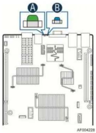
Figure 56. System Status LED (A) and ID LED (B)
Table 75. System Status LED
| Color | State | Criticality | Description |
| Green | Solid on | Ok | Indicates that the System Status is “Healthy”. The system is not exhibiting any errors. AC power is present and the BMC has booted and manageability functionality is up and running. |
| Green | ~1 Hz blink | Degraded | System degraded:Redundancy loss such as power supply or fan. Applies only if the associated platform subsystem has redundancy capabilities.Fan warning or failure when the number of fully operational fans is more than minimum number and less than full resource number needed to cool the system.Non-critical threshold crossed – Temperature (including HSBP temp), voltage, input power to power supply, output current for main power rail from power supply and Processor Thermal Control (Therm Ctrl) sensors.Power supply predictive failure occurred while redundant power supply configuration was present.Unable to use all of the installed memory (more than 1 DIMM installed) ^1 .Correctable Errors over a threshold and migrating to a spare DIMM (memory sparing). This indicates that the user no longer has spared DIMMs indicating a redundancy lost condition.Corresponding DIMM LED lit.In mirrored configuration, when memory mirroring takes place and system loses memory redundancy.Battery failure.BMC executing in uBoot. (Indicated by Chassis ID blinking at 3Hz). System in degraded state (no manageability). BMC uBoot is running but has not transferred control to BMC Linux*. Server will be in this state 6-8 seconds after BMC reset while it pulls the Linux* image into flash.BMC booting Linux*. (Indicated by Chassis ID solid ON). System in degraded state (no manageability). Control has been passed from BMC uBoot to BMC Linux* itself. It will be in this state for ~10~20 seconds.BMC Watchdog has reset the BMC.Power Unit sensor offset for configuration error is asserted.HDD HSC is offline or degraded. |
| Amber | ~1 Hz blink | Non-critical | Non-fatal alarm – system is likely to fail:Critical threshold crossed – Voltage, temperature (including HSBP temp), input power to power supply, output current for main power rail from power supply and PROCHOT (Therm Ctrl) sensors.VRD Hot asserted.Minimum number of fans to cool the system not present or failed.Hard drive fault.Power Unit Redundancy sensor – Insufficient resources offset (indicates not enough power supplies present).In non-sparing and non-mirroring mode if the threshold ofcorrectable errors is crossed within the window1. |
| Amber | Solid on | Critical, non-recoverable | Fatal alarm – system has failed or shut down:CPU CATERR signal asserted.MSID mismatch detected (CATERR also asserts for this case).CPU 1 is missing.CPU ThermalTrip.No power good – power fault.DIMM failure when there is only 1 DIMM present and hence no good memory is present7.Runtime memory uncorrectable error in non-redundant mode8.DIMM Thermal Trip or equivalent.SSB Thermal Trip or equivalent.CPU ERR2 signal asserted.BMC\Video memory test failed (Chassis ID shows blue/solid-on for this condition).Both uBoot BMC FW images are bad (Chassis ID shows blue/solid-on for this condition).240VA fault. |
| Off | N/A | Not ready | AC power off |
Notes:
1. This is BIOS-Driven functionality through the IPMI "Set Fault Indication" command.
7.3.6 Chassis ID LED
The chassis ID LED provides a visual indication of a system being serviced. The state of the chassis ID LED is affected by the following:
- Toggled by the chassis ID button
- Controlled by the Chassis Identify command (IPMI)
■ Controlled by the Chassis Identify LED command (OEM)
Table 76. Chassis ID LED Indicator States
| State | LED State |
| Identify active through button | Solid on |
| Identify active through command | ~1 Hz blink |
| Off | Off |
There is no precedence or lock-out mechanism for the control sources. When a new request arrives, all previous requests are terminated. For example, if the chassis ID LED is blinking and the chassis ID button is pressed, the chassis ID LED changes to solid on. If the button is pressed again with no intervening commands, the chassis ID LED turns off.
7.4 I/O Connectors
7.4.1 PCI Express\* Connectors
The Intel ^® Server Board S2600JP uses three PCI Express* slots physically with different pin-out definition. Each riser slot has dedicated usage and cannot be used for normal PCIe based add-in card.
- Riser Slot 1: Riser to support PCIe x16 add-in card or GPGPU card
- Riser Slot 2: Riser to support PCIe x16 add-in card, GPGPU card, or Intel ^ IOM card
- Riser Slot 3: Riser to support PCIe x16 add-in card or GPGPU card
The pin-outs for the slots are shown in the following tables.
Table 77. PCI Express* x16 Riser Slot 1 Connector (J6A1)
| Pin | Pin Name | Description | Pin | Pin Name | Description |
| B1 | 12V | 20W 3.3V generated on riser | A1 | 12V | 20W 3.3V generated on riser |
| B2 | 12V | 66W for GPU | A2 | 12V | 66W for GPU |
| B3 | 12V | 66W for GPU | A3 | 12V | 66W for GPU |
| B4 | 12V | 66W for GPU | A4 | SMDATA | |
| B5 | SMCLK | A5 | 3.3VAUX | For wake on LAN | |
| B6 | 3.3VAUX | For wake on LAN | A6 | GPU_NODE_ON | can turn of 2U GPU power |
| B7 | GND | A7 | GPU_PWRGD | ||
| B8 | Tach9 | A8 | Tach11 | ||
| B9 | Tach8 | A9 | Tach10 | ||
| B10 | Tach7 | A10 | Tach6 | ||
| B11 | Spare | A11 | Spare | ||
| KEY | |||||
| B12 | Spare | A12 | PWM2 | GPU Fan speed control | |
| B13 | Spare | A13 | GND | ||
| B14 | GND | A14 | PERST# | ||
| B15 | SMBUS_R4 CLK | A15 | WAKE# | ||
| B16 | SMBUS_R4 DAT | A16 | GND | ||
| B17 | GND | A17 | REFCLK+ | Clock pair 1 | |
| B18 | PETxP0 | Tx Lane 0+ | A18 | REFCLK- | Clock pair 1 |
| B19 | PETxN0 | Tx Lane 0- | A19 | GND | |
| B20 | GND | A20 | PERxP0 | Rx Lane 0+ | |
| B21 | GND | A21 | PERxN0 | Rx Lane 0- | |
| B22 | PETxP1 | Tx Lane 1+ | A22 | GND | |
| B23 | PETxN1 | Tx Lane 1- | A23 | GND | |
| B24 | GND | A24 | PERxP1 | Rx Lane 1+ | |
| B25 | GND | A25 | PERxN1 | Rx Lane 1- | |
| B26 | PETxP2 | Tx Lane 2+ | A26 | GND | |
| B27 | PETxN2 | Tx Lane 2- | A27 | GND | |
| B28 | GND | A28 | PERxP2 | Rx Lane 2+ | |
| B29 | GND | A29 | PERxN2 | Rx Lane 2- | |
| B30 | PETxP3 | Tx Lane 3+ | A30 | GND | |
| B31 | PETxN3 | Tx Lane 3- | A31 | GND | |
| B32 | GND | A32 | PERxP3 | Rx Lane 3+ | |
| B33 | GND | A33 | PERxN3 | Rx Lane 3- | |
| B34 | PETxP4 | Tx Lane 4+ | A34 | GND | |
| B35 | PETxN4 | Tx Lane 4- | A35 | GND | |
| B36 | GND | A36 | PERxP4 | Rx Lane 4+ | |
| B37 | GND | A37 | PERxN4 | Rx Lane 4- | |
| B38 | PETxP5 | Tx Lane 5+ | A38 | GND | |
| B39 | PETxN5 | Tx Lane 5- | A39 | GND | |
| B40 | GND | A40 | PERxP5 | Rx Lane 5+ | |
| B41 | GND | A41 | PERxN5 | Rx Lane 5- | |
| B42 | PETxP6 | Tx Lane 6+ | A42 | GND | |
| B43 | PETxN6 | Tx Lane 6- | A43 | GND | |
| B44 | GND | A44 | PERxP6 | Rx Lane 6+ | |
| B45 | GND | A45 | PERxN6 | Rx Lane 6- | |
| B46 | PETxP7 | Tx Lane 7+ | A46 | GND | |
| B47 | PETxN7 | Tx Lane 7- | A47 | GND | |
| B48 | GND | A48 | PERxP7 | Rx Lane 7+ | |
| B49 | GND | A49 | PERxN7 | Rx Lane 7- | |
| B50 | PETxP8 | Tx Lane 8+ | A50 | GND | |
| B51 | PETxN8 | Tx Lane 8- | A51 | GND | |
| B52 | GND | A52 | PERxP8 | Rx Lane 8+ | |
| B53 | GND | A53 | PERxN8 | Rx Lane 8- | |
| B54 | PETxP9 | Tx Lane 9+ | A54 | GND | |
| B55 | PETxN9 | Tx Lane 9- | A55 | GND | |
| B56 | GND | A56 | PERxP9 | Rx Lane 9+ | |
| B57 | GND | A57 | PERxN9 | Rx Lane 9- | |
| B58 | PETxP10 | Tx Lane 10+ | A58 | GND | |
| B59 | PETxN10 | Tx Lane 10- | A59 | GND | |
| B60 | GND | A60 | PERxP10 | Rx Lane 10+ | |
| B61 | GND | A61 | PERxN10 | Rx Lane 10- | |
| B62 | PETxP11 | Tx Lane 11+ | A62 | GND | |
| B63 | PETxN11 | Tx Lane 11- | A63 | GND | |
| B64 | GND | A64 | PERxP11 | Rx Lane 11+ | |
| B65 | GND | A65 | PERxN11 | Rx Lane 11- | |
| B66 | PETxP12 | Tx Lane 12+ | A66 | GND | |
| B67 | PETxN12 | Tx Lane 12- | A67 | GND | |
| B68 | GND | A68 | PERxP12 | Rx Lane 12+ | |
| B69 | GND | A69 | PERxN12 | Rx Lane 12- | |
| B70 | PETxP13 | Tx Lane 13+ | A70 | GND | |
| B71 | PETxN13 | Tx Lane 13- | A71 | GND | |
| B72 | GND | A72 | PERxP13 | Rx Lane 13+ | |
| B73 | GND | A73 | PERxN13 | Rx Lane 13- | |
| B74 | PETxP14 | Tx Lane 14+ | A74 | GND | |
| B75 | PETxN14 | Tx Lane 14- | A75 | GND | |
| B76 | GND | A76 | PERxP14 | Rx Lane 14+ | |
| B77 | REFCLK+ | Clock pair 2 | A77 | PERxN14 | Rx Lane 14- |
| B78 | REFCLK- | Clock pair 2 | A78 | GND | |
| B79 | GND | A79 | PERxP15 | Rx Lane 15+ | |
| B80 | PETxP15 | Tx Lane 15+ | A80 | PERxN15 | Rx Lane 15- |
| B81 | PETxN15 | Tx Lane 15- | A81 | GND | |
| B82 | GND | A82 | Riser ID | (See Table 80) | |
Table 78. PCI Express* x16 Riser Slot 2 Connector (J1A3)
| Pin | Pin Name | Description | Pin | Pin Name | Description |
| B1 | 12V | 20W 3.3V generated on riser | A1 | 12V | 20W 3.3V generated on riser |
| B2 | 12V | 66W for GPU | A2 | 12V | 66W for GPU |
| B3 | 12V | 66W for GPU | A3 | 12V | 66W for GPU |
| B4 | 12V | 66W for GPU | A4 | SMDATA | for rIOM temp sensor |
| B5 | SMCLK | for rIOM temp sensor | A5 | 5VAUX | For DNM and IOM wake on LAN |
| B6 | 3.3V Aux | For DNM and IOM wake on LAN | A6 | PRESENT# | DNM function present |
| B7 | GND | A7 | RIOM_ACT# | ||
| B8 | TXD_0 | RGMII txmit data | A8 | RXD_3 | RGMII receive data |
| B9 | TXD_1 | RGMII txmit data | A9 | RXD_2 | RGMII receive data |
| B10 | TXD_2 | RGMII txmit data | A10 | RXD_1 | RGMII receive data |
| B11 | TXD_3 | RGMII txmit data | A11 | RXD_0 | RGMII receive data |
| KEY | |||||
| B12 | GND | A12 | RX_CTL | RGMII receive Cntrl | |
| B13 | TX_CLK | RGMII txmit Clock | A13 | GND | |
| B14 | TX_CTL | RGMII txmit Cntrl | A14 | RX_CLK | RGMII receive Clock |
| B15 | MDIO | A15 | MDC | ||
| B16 | PERST# | A16 | GND | ||
| B17 | WAKE# | A17 | REFCLK+ | Clock pair 1 | |
| B18 | PETxP0 | Tx Lane 0+ | A18 | REFCLK- | Clock pair 1 |
| B19 | PETxN0 | Tx Lane 0- | A19 | GND | |
| B20 | GND | A20 | PERxP0 | Rx Lane 0+ | |
| B21 | GND | A21 | PERxN0 | Rx Lane 0- | |
| B22 | PETxP1 | Tx Lane 1+ | A22 | GND | |
| B23 | PETxN1 | Tx Lane 1- | A23 | GND | |
| B24 | GND | A24 | PERxP1 | Rx Lane 1+ | |
| B25 | GND | A25 | PERxN1 | Rx Lane 1- | |
| B26 | PETxP2 | Tx Lane 2+ | A26 | GND | |
| B27 | PETxN2 | Tx Lane 2- | A27 | GND | |
| B28 | GND | A28 | PERxP2 | Rx Lane 2+ | |
| B29 | GND | A29 | PERxN2 | Rx Lane 2- | |
| B30 | PETxP3 | Tx Lane 3+ | A30 | GND | |
| B31 | PETxN3 | Tx Lane 3- | A31 | GND | |
| B32 | GND | A32 | PERxP3 | Rx Lane 3+ | |
| B33 | GND | A33 | PERxN3 | Rx Lane 3- | |
| B34 | PETxP4 | Tx Lane 4+ | A34 | GND | |
| B35 | PETxN4 | Tx Lane 4- | A35 | GND | |
| B36 | GND | A36 | PERxP4 | Rx Lane 4+ | |
| B37 | GND | A37 | PERxN4 | Rx Lane 4- | |
| B38 | PETxP5 | Tx Lane 5+ | A38 | GND | |
| B39 | PETxN5 | Tx Lane 5- | A39 | GND | |
| B40 | GND | A40 | PERxP5 | Rx Lane 5+ | |
| B41 | GND | A41 | PERxN5 | Rx Lane 5- | |
| B42 | PETxP6 | Tx Lane 6+ | A42 | GND | |
| B43 | PETxN6 | Tx Lane 6- | A43 | GND | |
| B44 | GND | A44 | PERxP6 | Rx Lane 6+ | |
| B45 | GND | A45 | PERxN6 | Rx Lane 6- | |
| B46 | PETxP7 | Tx Lane 7+ | A46 | GND | |
| B47 | PETxN7 | Tx Lane 7- | A47 | GND | |
| B48 | GND | A48 | PERxP7 | Rx Lane 7+ | |
| B49 | GND | A49 | PERxN7 | Rx Lane 7- | |
| B50 | PETxP8 | Tx Lane 8+ | A50 | GND | |
| B51 | PETxN8 | Tx Lane 8- | A51 | GND | |
| B52 | GND | A52 | PERxP8 | Rx Lane 8+ | |
| B53 | GND | A53 | PERxN8 | Rx Lane 8- | |
| B54 | PETxP9 | Tx Lane 9+ | A54 | GND | |
| B55 | PETxN9 | Tx Lane 9- | A55 | GND | |
| B56 | GND | A56 | PERxP9 | Rx Lane 9+ | |
| B57 | GND | A57 | PERxN9 | Rx Lane 9- | |
| B58 | PETxP10 | Tx Lane 10+ | A58 | GND | |
| B59 | PETxN10 | Tx Lane 10- | A59 | GND | |
| B60 | GND | A60 | PERxP10 | Rx Lane 10+ | |
| B61 | GND | A61 | PERxN10 | Rx Lane 10- | |
| B62 | PETxP11 | Tx Lane 11+ | A62 | GND | |
| B63 | PETxN11 | Tx Lane 11- | A63 | GND | |
| B64 | GND | A64 | PERxP11 | Rx Lane 11+ | |
| B65 | GND | A65 | PERxN11 | Rx Lane 11- | |
| B66 | PETxP12 | Tx Lane 12+ | A66 | GND | |
| B67 | PETxN12 | Tx Lane 12- | A67 | GND | |
| B68 | GND | A68 | PERxP12 | Rx Lane 12+ | |
| B69 | GND | A69 | PERxN12 | Rx Lane 12- | |
| B70 | PETxP13 | Tx Lane 13+ | A70 | GND | |
| B71 | PETxN13 | Tx Lane 13- | A71 | GND | |
| B72 | GND | A72 | PERxP13 | Rx Lane 13+ | |
| B73 | GND | A73 | PERxN13 | Rx Lane 13- | |
| B74 | PETxP14 | Tx Lane 14+ | A74 | GND | |
| B75 | PETxN14 | Tx Lane 14- | A75 | GND | |
| B76 | GND | A76 | PERxP14 | Rx Lane 14+ | |
| B77 | REFCLK+ | Clock pair 2 | A77 | PERxN14 | Rx Lane 14- |
| B78 | REFCLK- | Clock pair 2 | A78 | GND | |
| B79 | GND | A79 | PERxP15 | Rx Lane 15+ | |
| B80 | PETxP15 | Tx Lane 15+ | A80 | PERxN15 | Rx Lane 15- |
| B81 | PETxN15 | Tx Lane 15- | A81 | GND | |
| B82 | GND | A82 | Riser ID | (See Table 80) | |
Table 79. PCI Express* x16 Riser Slot 3 Connector (J1H1)
| Pin | Pin Name | Description | Pin | Pin Name | Description |
| B1 | 12V | 20W 3.3V generated on riser | A1 | 12V | 20W 3.3V generated on riser |
| B2 | 12V | 66W for GPU | A2 | 12V | 66W for GPU |
| B3 | 12V | 66W for GPU | A3 | 12V | 66W for GPU |
| B4 | 12V | 66W for GPU | A4 | SMDATA | |
| B5 | SMCLK | A5 | 3.3VAUX | For wake on LAN | |
| B6 | 3.3VAUX | For wake on LAN | A6 | Spare | |
| B7 | GND | A7 | Spare | ||
| B8 | Spare | A8 | Spare | ||
| B9 | Spare | A9 | Spare | ||
| B10 | Spare | A10 | Spare | ||
| B11 | Spare | A11 | Spare | ||
| KEY | |||||
| B12 | GND | A12 | Spare | ||
| B13 | PERST# | A13 | GND | ||
| B14 | WAKE# | A14 | REFCLK+ | Clock pair 1 | |
| B15 | GND | A15 | REFCLK- | Clock pair 1 | |
| B16 | REFCLK+ | Clock pair 2 | A16 | GND | |
| B17 | REFCLK- | Clock pair 2 | A17 | GND | |
| B18 | GND | A18 | PERxP0 | Rx Lane 0+ | |
| B19 | GND | A19 | PERxN0 | Rx Lane 0- | |
| B20 | PETxP0 | Tx Lane 0+ | A20 | GND | |
| B21 | PETxN0 | Tx Lane 0- | A21 | GND | |
| B22 | GND | A22 | PERxP1 | Rx Lane 1+ | |
| B23 | GND | A23 | PERxN1 | Rx Lane 1- | |
| B24 | PETxP1 | Tx Lane 1+ | A24 | GND | |
| B25 | PETxN1 | Tx Lane 1- | A25 | GND | |
| B26 | GND | A26 | PERxP2 | Rx Lane 2+ | |
| B27 | GND | A27 | PERxN2 | Rx Lane 2- | |
| B28 | PETxP2 | Tx Lane 2+ | A28 | GND | |
| B29 | PETxN2 | Tx Lane 2- | A29 | GND | |
| B30 | GND | A30 | PERxP3 | Rx Lane 3+ | |
| B31 | GND | A31 | PERxN3 | Rx Lane 3- | |
| B32 | PETxP3 | Tx Lane 3+ | A32 | GND | |
| B33 | PETxN3 | Tx Lane 3- | A33 | GND | |
| B34 | GND | A34 | PERxP4 | Rx Lane 4+ | |
| B35 | GND | A35 | PERxN4 | Rx Lane 4- | |
| B36 | PETxP4 | Tx Lane 4+ | A36 | GND | |
| B37 | PETxN4 | Tx Lane 4- | A37 | GND | |
| B38 | GND | A38 | PERxP5 | Rx Lane 5+ | |
| B39 | GND | A39 | PERxN5 | Rx Lane 5- | |
| B40 | PETxP5 | Tx Lane 5+ | A40 | GND | |
| B41 | PETxN5 | Tx Lane 5- | A41 | GND | |
| B42 | GND | A42 | PERxP6 | Rx Lane 6+ | |
| B43 | GND | A43 | PERxN6 | Rx Lane 6- | |
| B44 | PETxP6 | Tx Lane 6+ | A44 | GND | |
| B45 | PETxN6 | Tx Lane 6- | A45 | GND | |
| B46 | GND | A46 | PERxP7 | Rx Lane 7+ | |
| B47 | GND | A47 | PERxN7 | Rx Lane 7- | |
| B48 | PETxP7 | Tx Lane 7+ | A48 | GND | |
| B49 | PETxN7 | Tx Lane 7- | A49 | GND | |
| B50 | GND | A50 | PERxP8 | Rx Lane 8+ | |
| B51 | GND | A51 | PERxN8 | Rx Lane 8- | |
| B52 | PETxP8 | Tx Lane 8+ | A52 | GND | |
| B53 | PETxN8 | Tx Lane 8- | A53 | GND | |
| B54 | GND | A54 | PERxP9 | Rx Lane 9+ | |
| B55 | GND | A55 | PERxN9 | Rx Lane 9- | |
| B56 | PETxP9 | Tx Lane 9+ | A56 | GND | |
| B57 | PETxN9 | Tx Lane 9- | A57 | GND | |
| B58 | GND | A58 | PERxP10 | Rx Lane 10+ | |
| B59 | GND | A59 | PERxN10 | Rx Lane 10- | |
| B60 | PETxP10 | Tx Lane 10+ | A60 | GND | |
| B61 | PETxN10 | Tx Lane 10- | A61 | GND | |
| B62 | GND | A62 | PERxP11 | Rx Lane 11+ | |
| B63 | GND | A63 | PERxN11 | Rx Lane 11- | |
| B64 | PETxP11 | Tx Lane 11+ | A64 | GND | |
| B65 | PETxN11 | Tx Lane 11- | A65 | GND | |
| B66 | GND | A66 | PERxP12 | Rx Lane 12+ | |
| B67 | GND | A67 | PERxN12 | Rx Lane 12- | |
| B68 | PETxP12 | Tx Lane 12+ | A68 | GND | |
| B69 | PETxN12 | Tx Lane 12- | A69 | GND | |
| B70 | GND | A70 | PERxP13 | Rx Lane 13+ | |
| B71 | GND | A71 | PERxN13 | Rx Lane 13- | |
| B72 | PETxP13 | Tx Lane 13+ | A72 | GND | |
| B73 | PETxN13 | Tx Lane 13- | A73 | GND | |
| B74 | GND | A74 | PERxP14 | Rx Lane 14+ | |
| B75 | GND | A75 | PERxN14 | Rx Lane 14- | |
| B76 | PETxP14 | Tx Lane 14+ | A76 | GND | |
| B77 | PETxN14 | Tx Lane 14- | A77 | GND | |
| B78 | GND | A78 | PERxP15 | Rx Lane 15+ | |
| B79 | GND | A79 | PERxN15 | Rx Lane 15- | |
| B80 | PETxP15 | Tx Lane 15+ | A80 | GND | |
| B81 | PETxN15 | Tx Lane 15- | A81 | GND | |
| B82 | GND | A82 | Riser ID | (See Table 80) | |
Table 80. PCI Express* Riser ID Assignment
| CPU1 | CPU2 | ||
| Description | Riser ID (0) | Riser ID (1) | Riser ID (2) |
| Riser 1 1x16 | 1 | ||
| Riser 1 2x8 | 0 | ||
| Riser 2 1x16 | 1 | ||
| Riser 2 2x8 | 0* | ||
| Riser 3 1x16 | 1 | ||
| Riser 3 2x8 | 0 | ||
Notes:
- S2600JF board supports only one GPIO for slot 2 riser ID. However, there are three types of riser defined for Slot 2.
a. PCIe 1 x16 riser
b. PCIe 2 x 8 riser
c. IOM riser
- Riser 2 x8 and Riser IOM share the same riser ID as IOM riser.
Table 81. PCI Express* Clock Source by Slot
| PCI Express Clocks Source according Riser's Lane | |||
| PCIE SLOT RISER | X16 PCIE PIN | X8 (lane 0~7) PCIE PIN | X8 (8~15) PCIE PIN |
| SLOT 1 | PIN A17/A18 | PIN A17/A18 | PIN B77/B78 |
| SLOT 2 | PIN A17/A18 | PIN A17/A18 | PIN B77/B78 |
| SLOT 3 | PIN A14/A15 | PIN A14/A15 | PIN B16/B17 |
7.4.2 VGA Connector
The following table details the pin-out definition of the external VGA connector (J4A1).
Table 82. VGA External Video Connector (J4A1)
| Pin | Signal Name | Description |
| 1 | V_IO_R_CONN | Red (analog color signal R) |
| 2 | V_IO_G_CONN | Green (analog color signal G) |
| 3 | V_IO_B_CONN | Blue (analog color signal B) |
| 4 | TP_VID_CONN_B4 | No connection |
| 5 | GND | Ground |
| 6 | GND | Ground |
| 7 | GND | Ground |
| 8 | GND | Ground |
| 9 | TP_VID_CONN_B9 | No connection |
| 10 | GND | Ground |
| 11 | TP_VID_CONN_B11 | No connection |
| 12 | V_IO_DDCDAT | DDCDAT |
| 13 | V_IO_HSYNC_CONN | HSYNC (horizontal sync) |
| 14 | V_IO_VSYNC_CONN | VSYNC (vertical sync) |
| 15 | V_IO_DDCCLK | DDCCLK |
7.4.3 NIC Connectors
The server board provides two independent RJ-45 connectors on the back edge of the board (JA6A1, JA5A1). The pin-out for NIC connectors are identical and are defined in the following table.
Table 83. RJ-45 10/100/1000 NIC Connector Pin-out (JA6A1 and JA5A1)
| Pin | Signal Name |
| 1 | GND |
| 2 | P1V8_NIC |
| 3 | NIC_A_MDI3P |
| 4 | NIC_A_MDI3N |
| 5 | NIC_A_MDI2P |
| 6 | NIC_A_MDI2N |
| 7 | NIC_A_MDI1P |
| 8 | NIC_A_MDI1N |
| 9 | NIC_A_MDI0P |
| 10 | NIC_A_MDI0N |
| 11 (D1) | NIC_LINKA_1000_N (LED |
| 12 (D2) | NIC_LINKA_100_N (LED) |
| 13 (D3) | NIC_ACT_LED_N |
| 14 | NIC_LINK_LED_N |
| 15 | GND |
| 16 | GND |
7.4.4 SATA Connectors
The server board provides one SATA port connector named SATA-1 port (J6D1) on board. Additional four SAS ports are provided through bridge board.
The pin configuration for each connector is identical and defined in the following table.
Table 84. SATA Connector
| Pin | Signal Name | Description |
| 1 | GND | Ground |
| 2 | SATA_TX_P | Positive side of transmit differential pair |
| 3 | SATA_TX_N | Negative side of transmit differential pair |
| 4 | GND | Ground |
| 5 | SATA_RX_N | Negative side of receive differential pair |
| 6 | SATA_RX_P | Positive side of receive differential pair |
| 7 | P5V_SATA/GND | +5V for DOM or Ground for SATA signals |
Note: SATA DOM requires external power that cannot be used with SATA-1 port.
7.4.5 Hard Drive Activity (Input) LED Header
Table 85. SATA HDD Activity (Input) LED Header (J6C5)
| Pin | Description |
| 1 | LED_HD_ACTIVE_L |
| 2 | NC |
7.4.6 Storage Upgrade Key Connector
The server board provides one SATA/SAS storage upgrade key connector (J6C4) on board. The Storage Upgrade Key is a small PCB board that has up to two security EEPROMs that are read by the system ME to enable different versions of LSI* RAID 5 software stack and/or upgrade from SATA to SAS storage functionality.
The pin configuration of connector is identical and defined in the following table.
Table 86. Storage Upgrade Key Connector (J6C4)
| Pin | Signal Description |
| 1 | GND |
| 2 | DYN_SKU_KEY |
| 3 | GND |
| 4 | SAS_SATA_RAID_KEY |
7.4.7 Serial Port Connectors
The server board provides one internal 9-pin serial A header (J6A2). The following tables define the pin-outs.
Table 87. Internal 9-Pin Serial A (COM1) (J6A2)
| Pin | Signal Name | Pin | Signal Name |
| 1 | SPB_DCD | 2 | SPB_DSR |
| 3 | SPB_SIN_N | 4 | SPB_RTS |
| 5 | SPB_SOUT_N | 6 | SPB_CTS |
| 7 | SPB_DTR | 8 | SPB_RI |
| 9 | GND |
7.4.8 USB Connectors
The following table details the pin-out of the external stack USB port 0/1 connectors (J3A1) found on the back edge of the server board.
Table 88. External USB Port Connector (J3A1)
| Pin | Signal Name | Description |
| 1 | +5V | USB Power |
| 2 | USB N | Differential data line paired with DATAH0 |
| 3 | USB P | Differential date line paired with DATAL0 |
| 4 | GND | Ground |
One 2x5 connector on the server board provides an option to support two additional internal USB port (USB 2/3). The pin-out is detailed in the following table.
Table 89. Internal USB Connector (J2D1)
| Pin | Signal Name | Pin | Signal Name |
| 1 | +5V | 2 | +5V |
| 3 | USB_N | 4 | USB_N |
| 5 | USB_P | 6 | USB_P |
| 7 | GND | 8 | GND |
| 9 | Key Pin | 10 | NC |
7.4.9 QSFP for InfiniBand\*
The following table details the pin-out of the QSFP connector (J2B1) found on the back edge of the server board. This port is only available on board SKU S2600JFQ and S2600JFF.
Table 90. QSFP Pin Definition
| Side A | Signal | Side B | Signal |
| 1 | GND | 1 | GND |
| 2 | IB_RX0_DN0 | 2 | IB_RX0_DN1 |
| 3 | IB_RX0_DP0 | 3 | IB_RX0_DP1 |
| 4 | GND | 4 | GND |
| 5 | IB_RX0_DN2 | 5 | IB_RX0_DN3 |
| 6 | IB_RX0_DP2 | 6 | IB_RX0_DP3 |
| 7 | GND | 7 | GND |
| 8 | SMB_IB_QSFP0_DATA | 8 | QSFP0_MODPRSL_N |
| 9 | SMB_IB_QSFP0_CLK | 9 | IRQ_QSFP0_N |
| 10 | P3V3_RX_PORT0 | 10 | P3V3_TX_PORT0 |
| 11 | RST_QSFP0_N | 11 | P3V3_PORT0 |
| 12 | FM_QSFP0_MODSEIL_N | 12 | QSFP0_LPMODE |
| 13 | GND | 13 | GND |
| 14 | IB_TX0_DP3 | 14 | IB_TX0_DP2 |
| 15 | IB_TX0_DN3 | 15 | IB_TX0_DN2 |
| 16 | GND | 16 | GND |
| 17 | IB_TX0_DP1 | 17 | IB_TX0_DP0 |
| 18 | IB_TX0_DN1 | 18 | IB_TX0_DN0 |
| 19 | GND | 19 | GND |
7.5 Fan Headers
To facilitate the connection of 3 x40mm double rotor fans, a 14-pin header is provided, and all fans share a PWM. Both rotor tachs can be monitored.
Table 91. Baseboard Fan Connector (J1K2)
| Pin | Signal Name | Pin | Signal Name |
| 1 | PWM1 | 2 | Reserved |
| 3 | Tach0 | 4 | Tach1 |
| 5 | Tach2 | 6 | Tach3 |
| 7 | Tach4 | 8 | Tach5 |
| 9 | NODE_ON | 10 | GND |
| 11 | SMBUS_R4 CLK | 12 | SMBUS_R4 DAT |
| 13 | NODE_ADR0 | 14 | NODE_PWRGD |
The SMBus* is used to connect to the hot-swap controller that provides inrush current protection and can measure the power being used by the node. The NODE_ON signal is used to turn on the hot-swap controller. Note that the polarity is correct because the ADI1275 controller uses a high true enable signal. When the node is turned off, the fans will continue to rotate at a preset
rate; this rate is selected by Intel and preset by the Fan manufacturer. This is done to stop air recirculation between nodes. When docking the board to a live 12V rail, the fans will spin up immediately; it may be required to phase their connection to power to minimize the inrush current. Bench testing of the fans should determine if this is necessary.
7.6 Chassis Intrusion
The Chassis Intrusion header is connected through a two-wire cable to a switch assembly that is mounted just under the chassis cover on systems that support this feature. When the chassis cover is removed, the switch and thus the electrical connection between the pins on this header become open allowing the Server Engines PILOT III BMC's CHASIS_N pin to be pulled LOW. The Server Engines PILOT III BMC's CHASIS_N pin is used by Firmware to note the change in the chassis cover status. Header on baseboard can be unstuffed by default a shorting resistor will be needed to close the circuit.
Table 92. Chassis Intrusion Header (J6C1)
| Header State | Description |
| PINS 1 and 2 CLOSED | BMC CHASIS_N is pulled HIGH. Chassis cover is closed. |
| PINS 1 and 2 OPEN | BMC CHASIS_N is pulled LOW. Chassis cover is removed. |
8. Intel ^® Light-Guided Diagnostics
The Intel ^® Server Board S2600JF has several on-board diagnostic LEDs to assist in troubleshooting board-level issues. This section describes the location and function of each LED on the server board.
8.1 Front Panel Support
The Intel ^® Server Board S2600JF supports Mini-FP on Intel ^® Server Chassis H2000JF. The front panel control signals are provided through bridge board.
Each Mini-FP provides the following switch and LED features:
- Power switch with integrated power LED (green). Includes clear button lens but painted black with laser etched power icon for light to shine through.
- Chassis ID switch with integrated ID LED (blue). Includes clear button lens but painted black with laser etched ID icon for light to shine through.
- Recessed resets switch with black actuator.
- Bi-color Status/Fault LED (green/amber). Includes a status/fault icon printed on cosmetic front panel label. Icon should be translucent (only shows when LED is on).
- Single network activity/link LED, hardware baseboard ORs Ethernet and Infiniband* activity signals together into just one global signal. Includes a network activity/link icon printed on cosmetic front panel label. Icon should be translucent (only shows when LED is on).
8.1.1 System ID LED
The server board supports a blue system ID LED on the front panel, which is used to visually identify a specific server installed among many other similar servers. There are two options available for illuminating the System ID LED:
- The front panel ID LED Button is pushed, which causes the LED to illuminate to a solid on state until the button is pushed again.
- An IPMI Chassis Identify command is remotely entered, which causes the LED to blink. The System ID LED on the server board is tied directly to the System ID LED on system front panel if present.
8.1.2 System Status LED
The server board supports status LED on the front panel, which acts as same as the status LED on the server board.
8.1.3 Network Link/Activity LED
The server board provides LED on the front panel for Network Link/Activity. On S2600JF base SKU, this LED shows the status of Ethernet port. On S2600JFQ and S2600JFF, this LED still shows the Ethernet port link and activities. Following table shows the LED detail.
Table 93. Network Link/Activity LED
| LED | Color | Condition | What It Means |
| LAN - Link/Activity | Green | On | LAN link/no access |
| Green | Blink | LAN access | |
| Off | Idle |
8.1.4 Dedicated InfiniBand\* Link/Activity LED
The server board provides dedicated LEDs for InfiniBand* Link/Activity. They are located on the baseboard rear, near diagnostic LED set. This set of LEDs only works on S2600JFQ and S2600JFF baseboard. See block B in Figure 59 for the location of LEDs. The following table shows the LED detail.
Table 94. InfiniBand* Link/Activity LED
| LED Color | LED State | NIC State |
| Amber (Right) | Off | No Logical Link |
| Blinking | Logical Link established | |
| Green (Left) | Off | No Physical Link |
| On | Physical Link established |
8.2 POST Code Diagnostic LEDs
Eight amber POST code diagnostic LEDs are located on the back left edge of the server board, in the rear I/O area near the QSFP connector.
During the system boot process, the BIOS executes a number of platform configuration processes, each of which is assigned a specific hex POST code number. As each configuration routine is started, the BIOS displays the given POST code to the POST code diagnostic LEDs on the back edge of the server board. To assist in troubleshooting a system hang during the POST process, you can use the Diagnostic LEDs to identify the last POST process executed. For a complete description of how these LEDs are read and a list of all supported POST codes, refer to Appendix A.
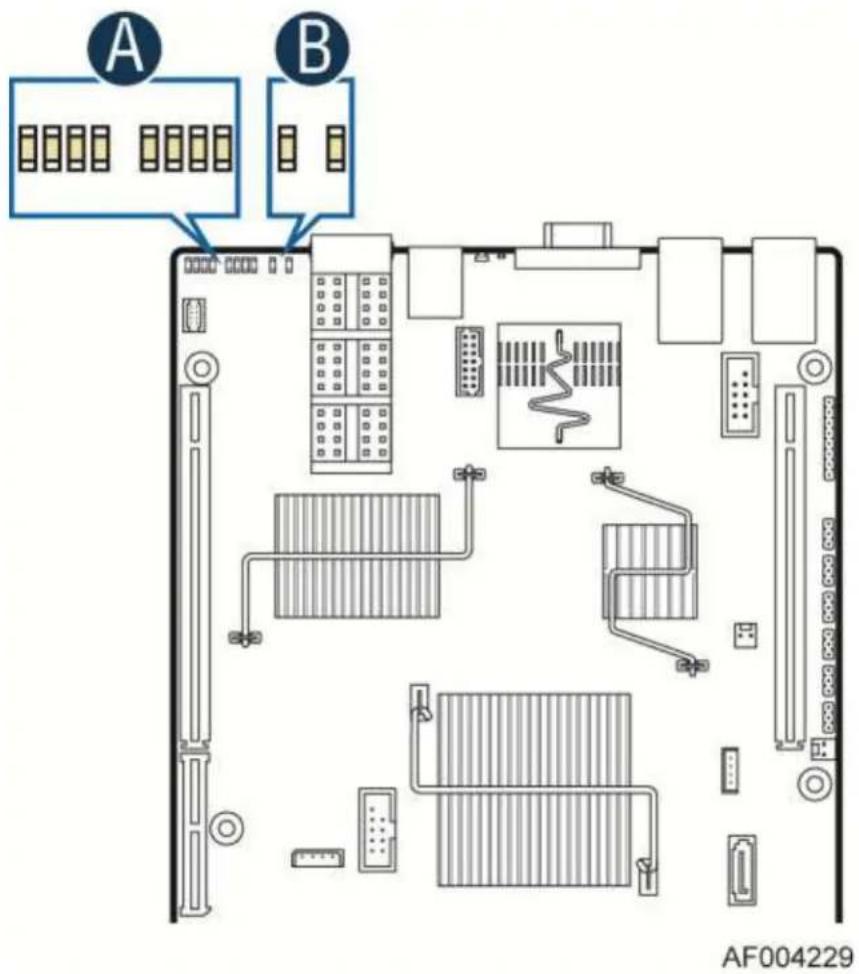
Figure 57. Rear Panel Diagnostic LEDs (Block A)
9. Environmental Limits Specification
Operation of the server board at conditions beyond those shown in the following table may cause permanent damage to the system. Exposure to absolute maximum rating conditions for extended periods may affect long term system reliability.
Note: The Energy Star compliance is at systems level, but not board level. Use of Intel ^® Server Boards alone does not guarantee Energy Star compliance.
Table 95. Server Board Design Specifications
| Operating Temperature | 0^ C to 55^ (32° F to 131° F) at product airflow specification |
| Non-Operating Temperature | -40° C to 70° C (-40° F to 158° F) |
| DC Voltage | ± 5% of all nominal voltages |
| Shock (Unpackaged) | Trapezoidal,35g, 170 inches/sec |
| Shock (Packaged)<20 pounds>= 20 to <40 pounds>= 40 to <80 pounds>= 80 to <100 pounds>= 100 to <120 pounds>= 120 pounds | 36 inches30 inches24 inches18 inches12 inches9 inches |
| Vibration (Unpackaged) | 5 Hz to 500 Hz3.13 g RMS random |
Note:
- Intel Corporation server boards contain a number of high-density VLSI and power delivery components that need adequate airflow to cool. Intel ensures through its own chassis development and testing that when Intel server building blocks are used together, the fully integrated system will meet the intended thermal requirements of these components. It is the responsibility of the system integrator who chooses not to use Intel developed server building blocks to consult vendor datasheets and operating parameters to determine the amount of airflow required for their specific application and environmental conditions. Intel Corporation cannot be held responsible, if components fail or the server board does not operate correctly when used outside any of its published operating or non-operating limits.
Disclaimer Note: Intel ensures the unpackaged server board and system meet the shock requirement mentioned above through its own chassis development and system configuration. It is the responsibility of the system integrator to determine the proper shock level of the board and system if the system integrator chooses different system configuration or different chassis. Intel Corporation cannot be held responsible if components fail or the server board does not operate correctly when used outside any of its published operating or non-operating limits.
9.1 System Level Environmental Considerations
In order to maintain comprehensive thermal protection, deliver the best system acoustics, and improve fan power efficiency, an intelligent Fan Speed Control (FSC) and thermal management technology (mechanism) is used. Options in
9.1.1 Set Throttling Mode
This option is used to select the desired memory thermal throttling mechanism. Available settings include [Auto], [DCLTT], [SCLTT] and [SOLTT].
[Auto] – Factory Default Setting: The BIOS automatically detects and identifies the appropriate thermal throttling mechanism based on DIMM type, airflow input, and DIMM sensor availability.
[DCLTT] – Dynamic Closed Loop Thermal Throttling: For the SOD DIMM with system airflow input.
[SCLTT] – Static Close Loop Thermal Throttling: For the SOD DIMM without system airflow input.
[SOLTT] – Static Open Loop Thermal Throttling: For the DIMMs without sensor on DIMM (SOD).
9.1.2 Altitude
This option is used to select the proper altitude that the system will be used in. Available settings include [300m or less], [301m-900m], [901m-1500m], and [Above 1500m].
Selecting an altitude range that is lower than the actual altitude the system will be operating at, can cause the fan control system to operate less efficiently, leading to higher system thermals and lower system performance. If the altitude range selected is higher than the actual altitude the system will be operating at, the fan control system may provide better cooling but with higher acoustics and higher fan power consumption. If the altitude is not known, selecting a higher altitude is recommended in order to provide sufficient cooling.
9.1.3 Set Fan Profile
This option is used to set the desired Fan Profile. Available settings include [Performance] and [Acoustic].
The Acoustic mode offers the best acoustic experience and appropriate cooling capability covering the mainstream and the majority of the add-in cards used. Performance mode is designed to provide sufficient cooling capability covering all kinds of add-in cards on the market.
9.1.4 Fan PWM Offset
This option is reserved for manual adjustment to the minimum fan speed curves. The valid range is from [0 to 100] that stands for 0% to 100% PWM adding to the minimum fan speed.
This feature is valid when Quiet Fan Idle Mode is at Enabled state. The default setting is [0].
9.1.5 Quiet Fan Idle Mode
This feature can be [Enabled] or [Disabled]. If enabled, the fans will either shift to lower speeds or stop when the aggregate sensor temperatures are satisfied, indicating the system is at ideal thermal/light loading conditions. When the aggregate sensor temperatures are not satisfied, the fans will shift back to normal control curves. If disabled, the fans will never shift to lower fan speeds or stop, regardless of whether the aggregate sensor temperatures are satisfied. The default setting is [Disabled].
Note: The features above may or may not be in effect and depend on the actual thermal characteristics of the specified system.
9.1.6 Thermal Sensor Input for Fan Speed Control
The BMC uses various IPMI sensors as inputs to fan speed control. Some of the sensors are actual physical sensors and some are “virtual” sensors derived from calculations.
The following IPMI thermal sensors are used as input to fan speed control:
■ Front Panel Temperature Sensor 1
■ Server board Temperature Sensor ^2
■ Processor Margin Sensors
■ DIMM Thermal Margin Sensors 3,5
■ Exit Air Temperature Sensor 1, 4, 8
Chipset Temperature Sensor ^4,6
- On-board Ethernet Controller Temperature Sensors ^4,6
- Add-In Intel ^ SAS/IO Module Temperature Sensors ^4,6
■ Power Supply Thermal Sensor 4,9
■ Processor VR Temperature Sensors 4,7
■ DIMM VR Temperature Sensors 4,7
■ BMC Temperature Sensor 4,7
■ Global Aggregate Thermal Margin Sensors ^8
Notes:
- For fan speed control in Intel chassis
- For fan speed control in third-party chassis
- Temperature margin from throttling threshold
- Absolute temperature
- PECI value or margin value
- On-die sensor
- On-board sensor
- Virtual sensor
- Available only when PSU has PMBus*
The following diagram illustrates the fan speed control structure.
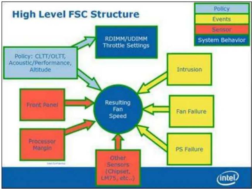
flowchart
graph TD
    A["RDIMM/UDIMM Throttle Settings"] --> B["Resulting Fan Speed"]
    C["Intrusion"] --> B
    D["Fan Failure"] --> B
    E["PS Failure"] --> B
    F["Other Sensors (Chipset, LM75, etc...)"] --> B
    G["Processor Margin"] --> B
    H["Front Panel"] --> B
    I["Policy: CLTT/OLTt, Acoustic/Performance, Altitude"] --> B
    J["System Behavior"] --> B
Figure 58. Fan Control Model
9.2 Processor Thermal Design Power (TDP) Support
To allow optimal operation and long-term reliability of Intel processor-based systems, the processor must remain within the defined minimum and maximum case temperature (TCASE) specifications. Thermal solutions not designed to provide sufficient thermal capability may affect the long-term reliability of the processor and system. The server board is designed to support the Intel® Xeon® Processor E5-2600 product family TDP guidelines up to and including 135W.
Disclaimer Note: Intel Corporation server boards contain a number of high-density VLSI and power delivery components that need adequate airflow to cool. Intel ensures through its own chassis development and testing that when Intel server building blocks are used together, the fully integrated system will meet the intended thermal requirements of these components. It is the responsibility of the system integrator who chooses not to use Intel-developed server building blocks to consult vendor datasheets and operating parameters to determine the amount of airflow required for their specific application and environmental conditions. Intel Corporation cannot be held responsible if components fail or the server board does not operate correctly when used outside any of their published operating or non-operating limits.
10. Power Supply Specification Guidelines
This section provides power supply specification guidelines recommended for providing the specified server platform with stable operating power requirements.
Note: The power supply data provided in this section is for reference purposes only. It reflects Intel's own DC power out requirements for a 1200W and 1600W power supply as used in an Intel designed 2U server platform. The intent of this section is to provide customers with a guide to assist in defining and/or selecting a power supply for custom server platform designs that utilize the server boards detailed in this document.
10.1 Power Supply DC Output Connector
The server board includes two main power Minifit Jr* connectors allowing for power supplies to attach directly to the server board. The connectors are two sets of 2x3 pin and can be used to deliver 12amps per pin or 60+Amps total. Note that no over-voltage protective circuits exist on the board.
Table 96. Power Supply DC Power Input Connector Pin-out (See Table 71)
| Pin | Signal Name | Pin | Signal Name |
| 1 | +12V | 4 | GND |
| 2 | +12V | 5 | GND |
| 3 | +12V | 6 | GND |
10.2 Power Supply DC Output Specification
10.2.1 Output Power/Currents
The following tables define the minimum power and current ratings. The power supply meets both static and dynamic voltage regulation requirements for all conditions.
Table 97. Minimum Load Ratings
| Parameter | Min | Max. | Peak^1,2 | Unit |
| 12V main | 0.0 | 60.0 | 72.0 | A |
| 5Vstby | 0.0 | 2.0 | 2.4 | A |
Notes:
- Peak combined power for all outputs shall not exceed 800W.
- Length of time peak power that can be supported is based on thermal sensor and assertion of the SMBAlert# signal. Minimum peak power duration shall be 20 seconds without asserting the SMBAlert# signal at maximum operating temperature.
10.2.2 Standby Output
The 5VSB output will be present when an AC input greater than the power supply turn on voltage is applied. There is load sharing in the standby rail.
10.2.3 Voltage Regulation
The power supply output voltages stay within the following voltage limits when operating at steady state and dynamic loading conditions. These limits include the peak-peak ripple/noise. These are measured at the output connectors.
Table 98. Voltage Regulation Limits
| Parameter | Tolerance | Min | Nom | Max | Units |
| +12V | -5%/+5% | +11.40 | +12.00 | +12.60 | V_rms |
| +5V stby | -5%/+5% | +4.75 | +5.00 | +5.25 | V_rms |
10.2.4 Dynamic Loading
The output voltages remain within limits specified for the step loading and capacitive loading specified in the following table. The load transient repetition rate is tested between 50Hz and 5kHz at duty cycles ranging from 10% to 90%. The load transient repetition rate is only a test specification. The step load may occur anywhere within the MIN load to the MAX load conditions.
Table 99. Transient Load Requirements
| Output | Δ Step Load Size | Load Slew Rate | Test capacitive Load |
| +5VSB | 1.0A | 0.25 A/μsec | 20 μF |
| +12V | 60% of max load | 0.25 A/μsec | 2000 μF |
Note: For dynamic condition +12V min loading is 1A.
10.2.5 Capacitive Loading
The power supply is stable and meets all requirements with the following capacitive loading ranges.
Table 100. Capacitive Loading Conditions
| Output | MIN | MAX | Units |
| +5VSB | 20 | 3100 | F |
| +12V | 500 | 25000 | F |
10.2.6 Grounding
The output ground of the pins of the power supply provides the output power return path. The output connector ground pins are connected to the safety ground (power supply enclosure). This grounding is well designed to ensure passing the max allowed Common Mode Noise levels.
The power supply is provided with a reliable protective earth ground. All secondary circuits are connected to protective earth ground. Resistance of the ground returns to chassis does not exceed 1.0 mΩ. This path may be used to carry DC current.
10.2.7 Closed Loop Stability
The power supply is unconditionally stable under all line/load/transient load conditions including specified capacitive load ranges. A minimum of 45 degrees phase margin and 10dB-gain margin is required. Closed-loop stability must be ensured at the maximum and minimum loads as applicable.
10.2.8 Residual Voltage Immunity in Standby Mode
The power supply is immune to any residual voltage placed on its outputs (Typically a leakage voltage through the system from standby output) up to 500mV. There is no additional heat generated, nor stressing of any internal components with this voltage applied to any individual or all outputs simultaneously. It also does not trip the protection circuits during turn on.
The residual voltage at the power supply outputs for no load condition does not exceed 100mV when AC voltage is applied and the PSON# signal is de-asserted.
10.2.9 Common Mode Noise
The Common Mode noise on any output does not exceed 350mV pk-pk over the frequency band of 10Hz to 20MHz.
10.2.10 Soft Starting
The Power Supply contains control circuit that provides monotonic soft start for its outputs without overstress of the AC line or any power supply components at any specified AC line or load conditions.
10.2.11 Zero Load Stability Requirements
When the power subsystem operates in a no load condition, it does not need to meet the output regulation specification, but it must operate without any tripping of over-voltage or other fault circuitry. When the power subsystem is subsequently loaded, it must begin to regulate and source current without fault.
10.2.12 Hot Swap Requirements
Hot swapping a power supply is the process of inserting and extracting a power supply from an operating power system. During this process the output voltages remain within the limits with the capacitive load specified. The hot swap test must be conducted when the system is operating under static, dynamic, and zero loading conditions.
10.2.13 Forced Load Sharing
The +12V output has active load sharing. The output shares within 10% at full load. The failure of a power supply does not affect the load sharing or output voltages of the other supplies still operating. The supplies can load share in parallel and operate in a hot-swap/redundant 1+1 configurations. The 12VSBoutput is not required to actively share current between power supplies (passive sharing). The 12VSBoutput of the power supplies are connected together in the system so that a failure or hot swap of a redundant power supply does not cause these outputs to go out of regulation in the system.
10.2.14 Ripple/Noise
The maximum allowed ripple/noise output of the power supply is defined in the following table. This is measured over a bandwidth of 10Hz to 20MHz at the power supply output connectors. A 10 F tantalum capacitor in parallel with a 0.1 F ceramic capacitor is placed at the point of measurement.
Table 101. Ripples and Noise
| +12V main | +5VSB |
| 120mVp-p | 50mVp-p |
10.2.15 Timing Requirement
These are the timing requirements for the power supply operation. The output voltages must rise from 10% to within regulation limits ( T_vout_rise ) within 5 to 70ms. For 5VSB, it is allowed to rise from 1.0 to 25ms. All outputs must rise monotonically. The following table shows the timing requirements for the power supply being turned on and off through the AC input, with PSON held low and the PSON signal, with the AC input applied.
Table 102. Timing Requirements
| Item | Description | Min | Max | Units |
| T_vout\_rise | Output voltage rise time. | 5.0 * | 70 * | ms |
| T_sb\_on\_delay | Delay from AC being applied to 5VSB being within regulation. | 1500 | ms | |
| T_ac\_on\_delay | Delay from AC being applied to all output voltages being within regulation. | 3000 | ms | |
| T_vout\_holdup | Time 12VI output voltage stays within regulation after loss of AC. | 13 | ms | |
| T_pwok\_holdup | Delay from loss of AC to de-assertion of PWOK. | 12 | ms | |
| T_pson\_on\_delay | Delay from PSON# active to output voltages within regulation limits. | 5 | 400 | ms |
| T_pson\_pwok | Delay from PSON# deactivate to PWOK being de-asserted. | 5 | ms | |
| T_pwok\_on | Delay from output voltages within regulation limits to PWOK asserted at turn on. | 100 | 500 | ms |
| T_pwok\_off | Delay from PWOK de-asserted to output voltages dropping out of regulation limits. | 1 | ms | |
| T_pwok\_low | Duration of PWOK being in the de-asserted state during an off/on cycle using AC or the PSON signal. | 100 | ms | |
| T_sb\_vout | Delay from 5VSB being in regulation to O/Ps being in regulation at AC turn on. | 50 | 1000 | ms |
| T_5VSB\_holdup | Time 5VSB output voltage stays within regulation after loss of AC. | 70 | ms |
Note:
* The 5VSB output voltage rise time shall be from 1.0ms to 25ms.
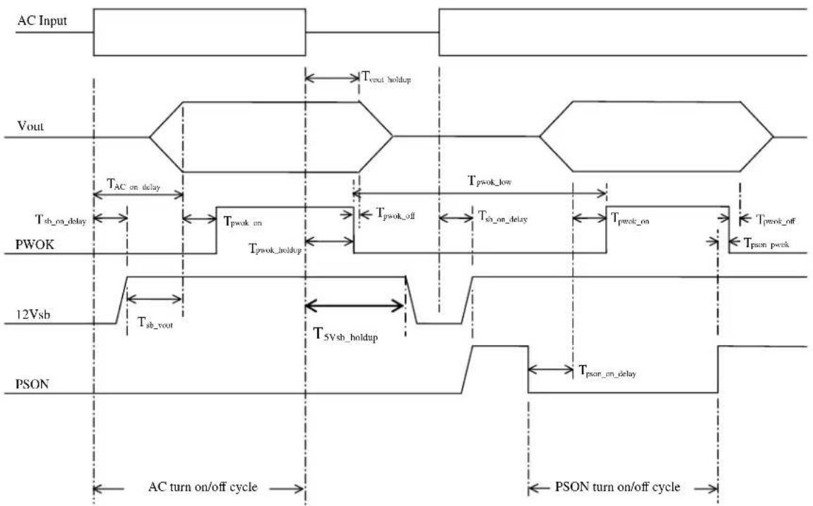
flowchart
graph TD
    A["AC Input"] --> B["Timing Diagram"]
    B --> C["Vout"]
    C --> D["Timing Diagram"]
    D --> E["PWOK"]
    E --> F["Timing Diagram"]
    F --> G["12Vsb"]
    G --> H["Timing Diagram"]
    H --> I["PSON"]
    I --> J["Timing Diagram"]

    subgraph Inputs
        B --> B1["T_pout_holdup"]
        C --> C1["T_AC_on_delay"]
        D --> D1["T_pwok_low"]
        E --> E1["T_sh_on_delay"]
        F --> F1["T_pwok_off"]
        G --> G1["T_sh_voot"]
        H --> H1["T_5Vsb_holdup"]
        I --> I1["T_pson_on_delay"]
        J --> J1["AC turn on/off cycle"]
        K --> K1["PSON turn on/off cycle"]
    end

    style Inputs fill:#f9f,stroke:#333
    style Vout fill:#ccf,stroke:#333
    style PWOK fill:#cfc,stroke:#333
    style 12Vsb fill:#fcc,stroke:#333
    style PSON fill:#cff,stroke:#333
Figure 59. Turn On/Off Timing (Power Supply Signals)
Appendix A: Integration and Usage Tips
- When adding or removing components or peripherals from the server board, AC power must be removed. With AC power plugged into the server board, 5V standby is still present even though the server board is powered off.
- This server board supports the Intel ^ Xeon ^ Processor E5-2600 and E5-2600V2 product family with a Thermal Design Power (TDP) of up to and including 135 Watts. Previous generations of the Intel ^ Xeon ^ processors are not supported.
- Processors must be installed in order. CPU 1 must be populated for the server board to operate.
- The server board includes a pre-installed CPU power cable harness. The cable harness must be installed and fully seated in each connector for the server board to operate.
- On the back edge of the server board are eight diagnostic LEDs that display a sequence of amber POST codes during the boot process. If the server board hangs during POST, the LEDs display the last POST event run before the hang.
- This server board only supports registered DDR3 DIMMs (RDIMMs) and unbuffered DDR3 DIMMs (UDIMMs). Mixing of RDIMMs and UDIMMs is not supported.
- For the best performance, the number of DDR3 DIMMs installed should be balanced across both processor sockets and memory channels. For example, a two-DIMM configuration performs better than a one-DIMM configuration. In a two-DIMM configuration, DIMMs should be installed in DIMM sockets A1 and D1. A six-DIMM configuration (DIMM sockets A1, B1, C1, D1, E1, and F1) performs better than a three-DIMM configuration (DIMM sockets A1, B1, and C1).
- The Intel ^ Remote Management Module 4 (Intel ^ RMM4) connector is not compatible with any previous versions of the Intel ^ Remote Management Module (Product Order Code – AXXRMM, AXXRMM2, and AXXRMM3).
- Clear the CMOS with AC power cord plugged. Removing the AC power before performing the CMOS clear operation causes the system to automatically power up and immediately power down after the CMOS clear procedure is followed and AC power is re-applied. If this happens, remove the AC power cord, wait 30 seconds, and then reconnect the AC power cord. Power up the system and proceed to the
BIOS Setup utility to reset the desired settings. - Normal Integrated BMC functionality is disabled with the BMC Force Update jumper set to the “enabled” position (pins 2-3). The server should never be run with the BMC Force Update jumper set in this position and should only be used when the standard firmware update process fails. This jumper should remain in the default (disabled) position (pins 1-2) when the server is running normally.
- When performing a normal BIOS update procedure, the BIOS recovery jumper must be set to its default position (pins 1-2).
Appendix B: Integrated BMC Sensor Tables
This appendix lists the sensor identification numbers and information about the sensor type, name, supported thresholds, assertion and de-assertion information, and a brief description of the sensor purpose. See the Intelligent Platform Management Interface Specification, Version 2.0, for sensor and event/reading-type table information.
- Sensor Type
The sensor type references the values in the Sensor Type Codes table in the Intelligent Platform Management Interface Specification Second Generation v2.0. It provides a context to interpret the sensor.
■ Event/Reading Type
The event/reading type references values from the Event/Reading Type Code Ranges and the Generic Event/Reading Type Code tables in the Intelligent Platform Management Interface Specification Second Generation v2.0. Digital sensors are specific type of discrete sensors that only have two states.
■ Event Thresholds/Triggers
The following event thresholds are supported for threshold type sensors: [u,l][nr,c,nc] upper non-recoverable, upper critical, upper non-critical, lower non-recoverable, lower critical, lower non-critical uc, lc upper critical, lower critical Event triggers are supported event-generating offsets for discrete type sensors. The offsets can be found in the Generic Event/Reading Type Code or Sensor Type Code tables in the Intelligent Platform Management Interface Specification Second Generation v2.0, depending on whether the sensor event/reading type is generic or a sensor-specific response.
- Assertion/Deassertion
Assertion and de-assertion indicators reveal the type of events this sensor generates:
As: Assertion
De: De-assertion
- Readable Value/Offsets
Readable value indicates the type of value returned for threshold and other non-discrete type sensors.
Readable offsets indicate the offsets for discrete sensors that are readable by means of the Get Sensor Reading command. Unless otherwise indicated, event triggers are readable. Readable offsets consist of the reading type offsets that do not generate events.
- Event Data
Event data is the data that is included in an event message generated by the associated sensor. For threshold-based sensors, these abbreviations are used:
R: Reading value
T: Threshold value
- Rearm Sensors
The rearm is a request for the event status for a sensor to be rechecked and updated upon a transition between good and bad states. Rearming the sensors can be done manually or automatically. This column indicates the type supported by the sensor. The following abbreviations are used in the comment column to describe a sensor:
A: Auto-rearm
M: Manual rearm
I: Rearm by init agent
- Default Hysteresis
The hysteresis setting applies to all thresholds of the sensor. This column provides the count of hysteresis for the sensor, which can be 1 or 2 (positive or negative hysteresis).
- Criticality
Criticality is a classification of the severity and nature of the condition. It also controls the behavior of the front panel status LED.
- Standby
Some sensors operate on standby power. These sensors may be accessed and/or generate events when the main (system) power is off, but AC power is present.
Table 103. BMC Sensor Table
| Full Sensor Name (Sensor name in SDR) | Sensor # | Platform Applicability | Sensor Type | Event/ Reading Type | Event Offset Triggers | Contrib. To System Status | Assert/De-assert | Readable Value/Offsets | Event Data | Ream | Stand-by |
| Power Unit Status (Pwr Unit Status) | 01h | All | Power Unit 09h | Sensor Specific 6Fh | 00 - Power down | OK | As and De | - | Trig Offset | A | X |
| 02 - 240 VA power down | Fatal | ||||||||||
| 04 - A/C lost | OK | ||||||||||
| 05 - Soft power control failure | Fatal | ||||||||||
| 06 - Power unit failure | |||||||||||
| Power Unit RedundancyNote1 (Pwr Unit Redund) | 02h | Chassis-specific | Power Unit 09h | Generic 0Bh | 00 - Fully Redundant | OK | As and De | - | Trig Offset | M | X |
| 01 - Redundancy lost | Degraded | ||||||||||
| 02 - Redundancy degraded | Degraded | ||||||||||
| 03 - Non-redundant: sufficient resources. Transition from full redundant state | Degraded | ||||||||||
| 04 - Non-redundant: sufficient resources. Transition from insufficient state | Degraded | ||||||||||
| 05 - Non-redundant: insufficient resources | Fatal | ||||||||||
| 06 - Redundant: degraded from fully redundant state | Degraded | ||||||||||
| 07 - Redundant: Transition from non-redundant state | Degraded |
Intel® Server Board S2600JF TPS Appendix B: Integrated BMC Sensor Tables
| Full Sensor Name (Sensor name in SDR) | Sensor # | Platform Applicability | Sensor Type | Event/ Reading Type | Event Offset Triggers | Contrib. To System Status | Assert/De-assert | Readable Value/Offsets | Event Data | Rearm | Stand-by |
| IPMI Watchdog (IPMI Watchdog) | 03h | All | Watchdog 2 23h | Sensor Specific 6Fh | 00 - Timer expired, status only | OK | As | - | Trig Offset | A | X |
| 01 - Hard reset | |||||||||||
| 02 - Power down | |||||||||||
| 03 - Power cycle | |||||||||||
| 08 - Timer interrupt | |||||||||||
| Physical Security (Physical Scrty) | 04h | Chassis Intrusion is chassis-specific | Physical Security 05h | Sensor Specific 6Fh | 00 - Chassis intrusion | OK | As and De | - | Trig Offset | A | X |
| 04 - LAN leash lost | |||||||||||
| FP Interrupt (FP NMI Diag Int) | 05h | Chassis - specific | Critical Interrupt 13h | Sensor Specific 6Fh | 00 - Front panel NMI/diagnostic interrupt | OK | As | - | Trig Offset | A | - |
| SMI Timeout (SMI Timeout) | 06h | All | SMI Timeout F3h | Digital Discrete 03h | 01 - State asserted | Fatal | As and De | - | Trig Offset | A | - |
| System Event Log (System Event Log) | 07h | All | Event Logging Disabled 10h | Sensor Specific 6Fh | 02 - Log area reset/cleared | OK | As | - | Trig Offset | A | X |
| System Event (System Event) | 08h | All | System Event 12h | Sensor Specific 6Fh | 02 - Undetermined system H/W failure 04 - PEF action | Fatal OK | As and De As | - | Trig Offset | A | X |
| Button Sensor (Button) | 09h | All | Button/Switch 14h | Sensor Specific 6Fh | 00 - Power Button 02 - Reset Button | OK | AS | - | Trig Offset | A | X |
| BMC Watchdog | 0Ah | All | Mgmt System Health 28h | Digital Discrete 03h | 01 - State Asserted | Degraded | As | - | Trig Offset | A | - |
| Voltage Regulator Watchdog (VR Watchdog) | 0Bh | All | Voltage 02h | Digital Discrete 03h | 01 - State Asserted | Fatal | As and De | - | Trig Offset | M | X |
| Fan RedundancyNote1 (Fan Redundancy) | 0Ch | Chassis-specific | Fan 04h | Generic 0Bh | 00 - Fully redundant | OK | As and De | - | Trig Offset | A | - |
| 01 - Redundancy lost | Degraded | ||||||||||
| 02 - Redundancy degraded | Degraded | ||||||||||
| 03 - Non-redundant: Sufficient resources. Transition from redundant | Degraded | ||||||||||
| 04 - Non-redundant: Sufficient resources. Transition from insufficient | Degraded | ||||||||||
| 05 - Non-redundant: insufficient resources | Non-Fatal | ||||||||||
| 06 - Non-Redundant: degraded from fully redundant | Degraded | ||||||||||
| 07 - Redundant degraded from non-redundant | Degraded | ||||||||||
| SSB Thermal Trip (SSB Therm Trip) | 0Dh | All | Temperature 01h | Digital Discrete 03h | 01 - State Asserted | Fatal | As and De | - | Trig Offset | M | X |
| IO Module Presence (IO Mod Presence) | 0Eh | Platform-specific | Module/Board 15h | Digital Discrete 08h | 01 - Inserted/Present | OK | As and De | - | Trig Offset | M | X |
| SAS Module Presence (SAS Mod Presence) | 0Fh | Platform-specific | Module/Board 15h | Digital Discrete 08h | 01 - Inserted/Present | OK | As and De | - | Trig Offset | M | X |
| BMC Firmware Health (BMC FW Health) | 10h | All | Mgmt Health 28h | Sensor Specific 6Fh | 04 - Sensor Failure | Degraded | As | - | Trig Offset | A | X |
Intel® Server Board S2600JF TPS Appendix B: Integrated BMC Sensor Tables
| Full Sensor Name (Sensor name in SDR) | Sensor # | Platform Applicability | Sensor Type | Event/ Reading Type | Event Offset Triggers | Contrib. To System Status | Assert/De-assert | Readable Value/Offsets | Event Data | Rearm | Stand-by |
| System Airflow (System Airflow) | 11h | All | Other Units 0Bh | Threshold 01h | - | - | - | Analog | - | - | - |
| FW Update Status | 0x12 | All | Version Change(0x2 B) | OEM defined(0 x70) | 1. 0x00h→Update started2. 0x01h→Update completed successfully0x02→Update failure | OK | As | - | Trig Offset | A | - |
| Baseboard Temperature 1 (Platform Specific) | 20h | Platform-specific | Temperature 01h | Threshold 01h | [u,l] [c,nc] | nc = Degraded c = Non-fatal | As and De | Analog | R, T | A | X |
| Front Panel Temperature (Front Panel Temp) | 21h | All | Temperature 01h | Threshold 01h | [u,l] [c,nc] | nc = Degraded c = Non-fatal | As and De | Analog | R, T | A | X |
| SSB Temperature (SSB Temp) | 22h | All | Temperature 01h | Threshold 01h | [u,l] [c,nc] | nc = Degraded c = Non-fatal | As and De | Analog | R, T | A | X |
| Baseboard Temperature 2 (Platform Specific) | 23h | Platform-specific | Temperature 01h | Threshold 01h | [u,l] [c,nc] | nc = Degraded c = Non-fatal | As and De | Analog | R, T | A | X |
| Baseboard Temperature 3 (Platform Specific) | 24h | Platform-specific | Temperature 01h | Threshold 01h | [u,l] [c,nc] | nc = Degraded c = Non-fatal | As and De | Analog | R, T | A | X |
| Baseboard Temperature 4 (Platform Specific) | 25h | Platform-specific | Temperature 01h | Threshold 01h | [u,l] [c,nc] | nc = Degraded c = Non-fatal | As and De | Analog | R, T | A | X |
| IO Module Temperature (I/O Mod Temp) | 26h | Platform-specific | Temperature 01h | Threshold 01h | [u,l] [c,nc] | nc = Degraded c = Non-fatal | As and De | Analog | R, T | A | X |
| PCI Riser 1 Temperature (PCI Riser 1 Temp) | 27h | Platform-specific | Temperature 01h | Threshold 01h | [u,l] [c,nc] | nc = Degraded c = Non-fatal | As and De | Analog | R, T | A | X |
| IO Riser Temperature (IO Riser Temp) | 28h | Platform-specific | Temperature 01h | Threshold 01h | [u,l] [c,nc] | nc = Degraded c = Non-fatal | As and De | Analog | R, T | A | X |
| Hot-swap Backplane 1 Temperature (HSBP 1 Temp) | 29h | Chassis-specific | Temperature 01h | Threshold 01h | [u,l] [c,nc] | nc = Degraded c = Non-fatal | As and De | Analog | R, T | A | X |
| Hot-swap Backplane 2 Temperature (HSBP 2 Temp) | 2Ah | Chassis-specific | Temperature 01h | Threshold 01h | [u,l] [c,nc] | nc = Degraded c = Non-fatal | As and De | Analog | R, T | A | X |
| Hot-swap Backplane 3 Temperature (HSBP 3 Temp) | 2Bh | Chassis-specific | Temperature 01h | Threshold 01h | [u,l] [c,nc] | nc = Degraded c = Non-fatal | As and De | Analog | R, T | A | X |
| PCI Riser 2 Temperature (PCI Riser 2 Temp) | 2Ch | Platform-specific | Temperature 01h | Threshold 01h | [u,l] [c,nc] | nc = Degraded c = Non-fatal | As and De | Analog | R, T | A | X |
| SAS Module Temperature (SAS Mod Temp) | 2Dh | Platform-specific | Temperature 01h | Threshold 01h | [u,l] [c,nc] | nc = Degraded c = Non-fatal | As and De | Analog | R, T | A | X |
Intel® Server Board S2600JF TPS Appendix B: Integrated BMC Sensor Tables
| Full Sensor Name (Sensor name in SDR) | Sensor # | Platform Applicability | Sensor Type | Event/ Reading Type | Event Offset Triggers | Contrib. To System Status | Assert/De-assert | Readable Value/Offsets | Event Data | Rearm | Stand-by |
| Exit Air Temperature (Exit Air Temp) | 2Eh | Chassis and Platform Specific | Temperature 01h | Threshold 01h | [u,l] [c,nc] | nc = Degraded c = Non-fatal | As and De | Analog | R, T | A | X |
| Network Interface Controller Temperature (LAN NIC Temp) | 2Fh | All | Temperature 01h | Threshold 01h | [u,l] [c,nc] | nc = Degraded c = Non-fatal | As and De | Analog | R, T | A | X |
| Fan Tachometer Sensors (Chassis specific sensor names) | 30h–3Fh | Chassis and Platform Specific | Fan 04h | Threshold 01h | [l] [c,nc] | nc = Degraded c = Non-fatal ^Note2 | As and De | Analog | R, T | M | - |
| Fan Present Sensors (Fan x Present) | 40h–4Fh | Chassis and Platform Specific | Fan 04h | Generic 08h | 01 - Device inserted | OK | As and De | - | Triggered Offset | Auto | - |
| Power Supply 1 Status (PS1 Status) | 50h | Chassis-specific | Power Supply 08h | Sensor Specific 6Fh | 00 - Presence | OK | As and De | - | Trig Offset | A | X |
| 01 - Failure | Degraded | ||||||||||
| 02 – Predictive Failure | Degraded | ||||||||||
| 03 - A/C lost | Degraded | ||||||||||
| 06 – Configuration error | OK | ||||||||||
| Power Supply 2 Status (PS2 Status) | 51h | Chassis-specific | Power Supply 08h | Sensor Specific 6Fh | 00 - Presence | OK | As and De | - | Trig Offset | A | X |
| 01 - Failure | Degraded | ||||||||||
| 02 – Predictive Failure | Degraded | ||||||||||
| 03 - A/C lost | Degraded | ||||||||||
| 06 – Configuration error | OK | ||||||||||
| Power Supply 1 AC Power Input (PS1 Power In) | 54h | Chassis-specific | Other Units 0Bh | Threshold 01h | [u] [c,nc] | nc = Degraded c = Non-fatal | As and De | Analog | R, T | A | X |
| Power Supply 2 AC Power Input (PS2 Power In) | 55h | Chassis-specific | Other Units 0Bh | Threshold 01h | [u] [c,nc] | nc = Degraded c = Non-fatal | As and De | Analog | R, T | A | X |
| Power Supply 1 +12V % of Maximum Current Output (PS1 Curr Out %) | 58h | Chassis-specific | Current 03h | Threshold 01h | [u] [c,nc] | nc = Degraded c = Non-fatal | As and De | Analog | R, T | A | X |
| Power Supply 2 +12V % of Maximum Current Output (PS2 Curr Out %) | 59h | Chassis-specific | Current 03h | Threshold 01h | [u] [c,nc] | nc = Degraded c = Non-fatal | As and De | Analog | R, T | A | X |
| Power Supply 1 Temperature (PS1 Temperature) | 5Ch | Chassis-specific | Temperature 01h | Threshold 01h | [u] [c,nc] | nc = Degraded c = Non-fatal | As and De | Analog | R, T | A | X |
| Power Supply 2 Temperature (PS2 Temperature) | 5Dh | Chassis-specific | Temperature | Threshold 01h | [u] [c,nc] | nc = Degraded c = Non-fatal | As and De | Analog | R, T | A | X |
| Hard Disk Drive 16 - 24 Status (HDD 16 - 24 Status) | 60h - 68h | Chassis-specific | Drive Slot 0Dh | Sensor Specific 6Fh | 00 - Drive Presence | OK | As and De | - | Trig Offset | A | X |
| 01 - Drive Fault | Degraded | ||||||||||
| 07 - Rebuild/Remap in progress | Degraded |
Intel® Server Board S2600JF TPS Appendix B: Integrated BMC Sensor Tables
| Full Sensor Name (Sensor name in SDR) | Sensor # | Platform Applicability | Sensor Type | Event/ Reading Type | Event Offset Triggers | Contrib. To System Status | Assert/De-assert | Readable Value/Offsets | Event Data | Rearm | Stand-by |
| HSC Status | 69h - 6Bh | Chassis-specific | Microcontrol er 16h | Discrete 0Ah | 04- transition to Off Line | Degraded | As and De | - | Trig Offset | A | X |
| Processor 1 Status (P1 Status) | 70h | All | Processor 07h | Sensor Specific 6Fh | 01 - Thermal trip | Fatal | As and De | - | Trig Offset | M | X |
| 07 - Presence | OK | ||||||||||
| Processor 2 Status (P2 Status) | 71h | All | Processor 07h | Sensor Specific 6Fh | 01 - Thermal trip | Fatal | As and De | - | Trig Offset | M | X |
| 07 - Presence | OK | ||||||||||
| Processor 1 Thermal Margin (P1 Therm Margin) | 74h | All | Temperature 01h | Threshold 01h | - | - | - | Analog | R, T | A | - |
| Processor 2 Thermal Margin (P2 Therm Margin) | 75h | All | Temperature 01h | Threshold 01h | - | - | - | Analog | R, T | A | - |
| Processor 1 Thermal Control % (P1 Therm Ctrl %) | 78h | All | Temperature 01h | Threshold 01h | [u] [c,nc] | nc = Degraded c = Non-fatal | As and De | Analog | Trig Offset | A | - |
| Processor 2 Thermal Control % (P2 Therm Ctrl %) | 79h | All | Temperature 01h | Threshold 01h | [u] [c,nc] | nc = Degraded c = Non-fatal | As and De | Analog | Trig Offset | A | - |
| Processor 1 ERR2 Timeout (P1 ERR2) | 7Ch | All | Processor 07h | Digital Discrete 03h | 01 - State Asserted | fatal | As and De | - | Trig Offset | A | - |
| Processor 2 ERR2 Timeout (P2 ERR2) | 7Dh | All | Processor 07h | Digital Discrete 03h | 01 - State Asserted | fatal | As and De | - | Trig Offset | A | - |
| Catastrophic Error (CATERR) | 80h | All | Processor 07h | Digital Discrete 03h | 01 - State Asserted | fatal | As and De | - | Trig Offset | M | - |
| Processor1 MSID Mismatch (P1 MSID Mismatch) | 81h | All | Processor 07h | Digital Discrete 03h | 01 – State Asserted | fatal | As and De | - | Trig Offset | M | - |
| Processor Population Fault (CPU Missing) | 82h | All | Processor 07h | Digital Discrete 03h | 01 – State Asserted | Fatal | As and De | - | Trig Offset | M | - |
| Processor 1 DTS Thermal Margin (P1 DTS Therm Mgn) | 83h | All | Temperature 01h | Threshold 01h | - | - | - | Analog | R, T | A | - |
| Processor 2 DTS Thermal Margin (P2 DTS Therm Mgn) | 83h | All | Temperature 01h | Threshold 01h | - | - | - | Analog | R, T | A | - |
| Processor2 MSID Mismatch (P2 MSID Mismatch) | 87h | All | Processor 07h | Digital Discrete 03h | 01 – State Asserted | fatal | As and De | - | Trig Offset | M | - |
| Processor 1 VRD Temperature (P1 VRD Hot) | 90h | All | Temperature 01h | Digital Discrete 05h | 01 - Limit exceeded | Non-fatal | As and De | - | Trig Offset | M | - |
| Processor 2 VRD Temperature (P2 VRD Hot) | 91h | All | Temperature 01h | Digital Discrete 05h | 01 - Limit exceeded | Non-fatal | As and De | - | Trig Offset | M | - |
| Processor 1 Memory VRD Hot 0-1 (P1 Mem01 VRD Hot) | 94h | All | Temperature 01h | Digital Discrete 05h | 01 - Limit exceeded | Non-fatal | As and De | - | Trig Offset | A | - |
| Processor 1 Memory VRD Hot 2-3 (P1 Mem23 VRD Hot) | 95h | All | Temperature 01h | Digital Discrete 05h | 01 - Limit exceeded | Non-fatal | As and De | - | Trig Offset | A | - |
Intel® Server Board S2600JF TPS Appendix B: Integrated BMC Sensor Tables
| Full Sensor Name (Sensor name in SDR) | Sensor # | Platform Applicability | Sensor Type | Event/ Reading Type | Event Offset Triggers | Contrib. To System Status | Assert/De-assert | Readable Value/Offsets | Event Data | Rearm | Stand-by |
| Processor 2 Memory VRD Hot 0-1 (P2 Mem01 VRD Hot) | 96h | All | Temperature 01h | Digital Discrete 05h | 01 - Limit exceeded | Non-fatal | As and De | - | Trig Offset | A | - |
| Processor 2 Memory VRD Hot 2-3 (P2 Mem23 VRD Hot) | 97h | All | Temperature 01h | Digital Discrete 05h | 01 - Limit exceeded | Non-fatal | As and De | - | Trig Offset | A | - |
| Power Supply 1 Fan Tachometer 1 (PS1 Fan Tach 1) | A0h | Chassis-specific | Fan 04h | Generic - digital discrete | 01 - State Asserted | Non-fatal | As and De | - | Trig Offset | M | - |
| Power Supply 1 Fan Tachometer 2 (PS1 Fan Tach 2) | A1h | Chassis-specific | Fan 04h | Generic - digital discrete | 01 - State Asserted | Non-fatal | As and De | - | Trig Offset | M | - |
| Power Supply 2 Fan Tachometer 1 (PS2 Fan Tach 1) | A4h | Chassis-specific | Fan 04h | Generic - digital discrete | 01 - State Asserted | Non-fatal | As and De | - | Trig Offset | M | - |
| Power Supply 2 Fan Tachometer 2 (PS2 Fan Tach 2) | A5h | Chassis-specific | Fan 04h | Generic - digital discrete | 01 - State Asserted | Non-fatal | As and De | - | Trig Offset | M | - |
| Processor 1 DIMM Aggregate Thermal Margin 1 (P1 DIMM Thrm Mrgn1) | B0h | All | Temperature 01h | Threshold 01h | [u,l] [c,nc] | nc = Degraded c = Non-fatal | As and De | Analog | R, T | A | - |
| Processor 1 DIMM Aggregate Thermal Margin 2 (P1 DIMM Thrm Mrgn2) | B1h | All | Temperature 01h | Threshold 01h | [u,l] [c,nc] | nc = Degraded c = Non-fatal | As and De | Analog | R, T | A | - |
| Processor 2 DIMM Aggregate Thermal Margin 1 (P2 DIMM Thrm Mrgn1) | B2h | All | Temperature 01h | Threshold 01h | [u,l] [c,nc] | nc = Degraded c = Non-fatal | As and De | Analog | R, T | A | - |
Revision 2.3 Intel order number G31608-014 171
| Full Sensor Name (Sensor name in SDR) | Sensor # | Platform Applicability | Sensor Type | Event/ Reading Type | Event Offset Triggers | Contrib. To System Status | Assert/De-assert | Readable Value/Offsets | Event Data | Rearm | Stand-by |
| Processor 2 DIMM Aggregate Thermal Margin 2 (P2 DIMM Thrm Mrgn2) | B3h | All | Temperature 01h | Threshold 01h | [u,l] [c,nc] | nc = Degraded c = Non-fatal | As and De | Analog | R, T | A | - |
| Processor 1 DIMM Thermal Trip (P1 Mem Thrm Trip) | C0h | All | Temperature 01h | Digital Discrete 03h | 01 - State Asserted | Fatal | As and De | - | Trig Offset | M | - |
| Processor 2 DIMM Thermal Trip (P2 Mem Thrm Trip) | C1h | All | Temperature 01h | Digital Discrete 03h | 01 - State Asserted | Fatal | As and De | - | Trig Offset | M | - |
| Global Aggregate Temperature Margin 1 (Agg Therm Mrgn 1) | C8h | Platform Specific | Temperature 01h | Threshold 01h | - | - | - | Analog | R, T | A | - |
| Global Aggregate Temperature Margin 2 (Agg Therm Mrgn 2) | C9h | Platform Specific | Temperature 01h | Threshold 01h | - | - | - | Analog | R, T | A | - |
| Global Aggregate Temperature Margin 3 (Agg Therm Mrgn 3) | CAh | Platform Specific | Temperature 01h | Threshold 01h | - | - | - | Analog | R, T | A | - |
| Global Aggregate Temperature Margin 4 (Agg Therm Mrgn 4) | CBh | Platform Specific | Temperature 01h | Threshold 01h | - | - | - | Analog | R, T | A | - |
Intel® Server Board S2600JF TPS Appendix B: Integrated BMC Sensor Tables
| Full Sensor Name (Sensor name in SDR) | Sensor # | Platform Applicability | Sensor Type | Event/ Reading Type | Event Offset Triggers | Contrib. To System Status | Assert/De-assert | Readable Value/Offsets | Event Data | Rearm | Stand-by |
| Global Aggregate Temperature Margin 5(Agg Therm Mrgn 5) | CCh | Platform Specific | Temperature 01h | Threshold 01h | - | - | - | Analog | R, T | A | - |
| Global Aggregate Temperature Margin 6(Agg Therm Mrgn 6) | CDh | Platform Specific | Temperature 01h | Threshold 01h | - | - | - | Analog | R, T | A | - |
| Global Aggregate Temperature Margin 7(Agg Therm Mrgn 7) | CEh | Platform Specific | Temperature 01h | Threshold 01h | - | - | - | Analog | R, T | A | - |
| Global Aggregate Temperature Margin 8(Agg Therm Mrgn 8) | CFh | Platform Specific | Temperature 01h | Threshold 01h | - | - | - | Analog | R, T | A | - |
| Baseboard +12V (BB +12.0V) | D0h | All | Voltage 02h | Threshold 01h | [u,l] [c,nc] | nc = Degraded c = Non-fatal | As and De | Analog | R, T | A | - |
| Baseboard +5V (BB +5.0V) | D1h | All | Voltage 02h | Threshold 01h | [u,l] [c,nc] | nc = Degraded c = Non-fatal | As and De | Analog | R, T | A | - |
| Baseboard +3.3V (BB +3.3V) | D2h | All | Voltage 02h | Threshold 01h | [u,l] [c,nc] | nc = Degraded c = Non-fatal | As and De | Analog | R, T | A | - |
| Baseboard +5V Stand-by (BB +5.0V STBY) | D3h | All | Voltage 02h | Threshold 01h | [u,l] [c,nc] | nc = Degraded c = Non-fatal | As and De | Analog | R, T | A | X |
| Baseboard +3.3V Auxiliary (BB +3.3V AUX) | D4h | All | Voltage 02h | Threshold 01h | [u,l] [c,nc] | nc = Degraded c = Non-fatal | As and De | Analog | R, T | A | X |
| Baseboard +1.05V Processor 1 Vccp (BB +1.05Vccp P1) | D6h | All | Voltage 02h | Threshold 01h | [u,l] [c,nc] | nc = Degraded c = Non-fatal | As and De | Analog | R, T | A | - |
| Baseboard +1.05V Processor 1 Vccp (BB +1.05Vccp P2) | D7h | All | Voltage 02h | Threshold 01h | [u,l] [c,nc] | nc = Degraded c = Non-fatal | As and De | Analog | R, T | A | - |
| Baseboard +1.5V P1 Memory AB VDDQ (BB +1.5 P1MEM AB) | D8h | All | Voltage 02h | Threshold 01h | [u,l] [c,nc] | nc = Degraded c = Non-fatal | As and De | Analog | R, T | A | - |
| Baseboard +1.5V P1 Memory CD VDDQ (BB +1.5 P1MEM CD) | D9h | All | Voltage 02h | Threshold 01h | [u,l] [c,nc] | nc = Degraded c = Non-fatal | As and De | Analog | R, T | A | - |
| Baseboard +1.5V P2 Memory AB VDDQ (BB +1.5 P2MEM AB) | DAh | All | Voltage 02h | Threshold 01h | [u,l] [c,nc] | nc = Degraded c = Non-fatal | As and De | Analog | R, T | A | - |
| Baseboard +1.5V P2 Memory CD VDDQ (BB +1.5 P2MEM CD) | DBh | All | Voltage 02h | Threshold 01h | [u,l] [c,nc] | nc = Degraded c = Non-fatal | As and De | Analog | R, T | A | - |
| Baseboard +1.8V Aux (BB +1.8V AUX) | DCh | All | Voltage 02h | Threshold 01h | [u,l] [c,nc] | nc = Degraded c = Non-fatal | As and De | Analog | R, T | A | - |
Intel® Server Board S2600JF TPS Appendix B: Integrated BMC Sensor Tables
| Full Sensor Name (Sensor name in SDR) | Sensor # | Platform Applicability | Sensor Type | Event/ Reading Type | Event Offset Triggers | Contrib. To System Status | Assert/De-assert | Readable Value/Offsets | Event Data | Rearm | Stand-by |
| Baseboard +1.1V Stand-by (BB +1.1V STBY) | DDh | All | Voltage 02h | Threshold 01h | [u,l] [c,nc] | nc = Degraded c = Non-fatal | As and De | Analog | R, T | A | - |
| Baseboard CMOS Battery (BB +3.3V Vbat) | DEh | All | Voltage 02h | Threshold 01h | [u,l] [c,nc] | nc = Degraded c = Non-fatal | As and De | Analog | R, T | A | - |
| Baseboard +1.35V P1 Low Voltage Memory AB VDDQ (BB +1.35 P1LV AB) | E4h | All | Voltage 02h | Threshold 01h | [u,l] [c,nc] | nc = Degraded c = Non-fatal | As and De | Analog | R, T | A | - |
| Baseboard +1.35V P1 Low Voltage Memory CD VDDQ (BB +1.35 P1LV CD) | E5h | All | Voltage 02h | Threshold 01h | [u,l] [c,nc] | nc = Degraded c = Non-fatal | As and De | Analog | R, T | A | - |
| Baseboard +1.35V P2 Low Voltage Memory AB VDDQ (BB +1.35 P2LV AB) | E6h | All | Voltage 02h | Threshold 01h | [u,l] [c,nc] | nc = Degraded c = Non-fatal | As and De | Analog | R, T | A | - |
| Baseboard +1.35V P2 Low Voltage Memory CD VDDQ (BB +1.35 P2LV CD) | E7h | All | Voltage 02h | Threshold 01h | [u,l] [c,nc] | nc = Degraded c = Non-fatal | As and De | Analog | R, T | A | - |
| Baseboard +3.3V Riser 1 Power Good (BB +3.3 RSR1 PGD) | EAh | Platform Specific | Voltage 02h | Threshold 01h | [u,l] [c,nc] | nc = Degraded c = Non-fatal | As and De | Analog | R, T | A | - |
| Baseboard +3.3V Riser 2 Power Good (BB +3.3 RSR2 PGD) | EBh | Platform Specific | Voltage 02h | Threshold 01h | [u,l] [c,nc] | nc = Degraded c = Non-fatal | As and De | Analog | R, T | A | - |
| Hard Disk Drive 1 - 15 Status (HDD 1 - 15 Status) | F0h - FEh | Chassis-specific | Drive Slot 0Dh | Sensor Specific 6Fh | 00 - Drive Presence | OK | As and De | - | Trig Offset | A | X |
| 01- Drive Fault | Degraded | ||||||||||
| 07 - Rebuild/Remap in progress | Degraded |
Notes:
1. Redundancy sensors will be only present on systems with appropriate hardware to support redundancy (for instance, fan or power supply).
2. This is only applicable when the system does not support redundant fans. When fan redundancy is supported, the contribution to system state is driven by the fan redundancy sensor.
Appendix C: BIOS Sensors and SEL Data
The BIOS owns a set of IPMI-compliant Sensors. These are actually divided in ownership between BIOS POST (GID = 01) and BIOS SMI Handler (GID = 33). The SMI Handler Sensors are typically for logging runtime error events, but they are active during POST and may log errors such as Correctable Memory ECC Errors if they occur.
It is important to remember that a Sensor is uniquely identified by the combination of Sensor Owner plus Sensor Number. There are cases where the same Sensor Number is used with different Sensor Owners – this is not a conflict. For example, in the BIOS Sensors list there is a Sensor Number 83h for Sensor Owner 01h (BIOS POST) as well as for Sensor Owner 33h (SMI Handler), but these are two distinct sensors reporting the same type of event from different sources (Generator IDs 01h and 33h).
On the other hand, each distinct Sensor (GID + Sensor Number) is defined by one specific Sensor Type describing the kind of data being reported, and one specific Event Type describing the type of event and the format of the data being reported.
Table 104. BIOS Sensor and SEL Data
| Sensor Name | Sensor Number | Sensor Owner (GID) | Sensor Type | Event/Reading Type Offset Values | Event Data 2 Event Data 3 |
| Mirroring Redundancy State | 01h | 33h (SMI Handler) | 0Ch (Memory) | 0Bh (Discrete, Redundancy State)0h = Fully Redundant2h = Redundancy Degraded | ED2 = [7:4] = Mirroring Domain0-1 = Channel Pair for Socket [3:2] = Reserved [1:0] = Rank on DIMM0-3 = Rank NumberED3 = [7:5]= Socket ID0-3 = CPU1-4[4:3] = Channel0-3 = Channel A-D for Socket [2:0] = DIMM0-2 = DIMM 1-3 on Channel |
| Memory RAS Configuration Status | 02h | 01h (BIOS POST) | 0Ch (Memory) | 09h (Digital Discrete)0h = RASConfiguration Disabled1h = RASConfiguration Enabled | ED2 = [7:4] = Reserved[3:0] Config Err0 = None3 = InvalidDIMM Config for RAS ModeED3 = [7:4] = Reserved[3:0] = RASMode0 = None1 = Mirroring2 = Lockstep4 = RankSparing |
| Memory ECC Error | 02h | 33h (SMI Handler) | 0Ch (Memory) | 6Fh (Sensor Specific Offset)0h = Correctable Error1h = Uncorrectable Error | ED2 = [7:2] = Reserved[1:0] = Rank on DIMM0-3 = RankNumberED3 = [7:5]= Socket ID0-3 = CPU1-4[4:3] = Channel0-3 = ChannelA-D for Socket[2:0] = DIMM0-2 = DIMM 1-3 on Channel |
| Legacy PCI Error | 03h | 33h (SMI Handler) | 13h (Critical Interrupt) | 6Fh (Sensor Specific Offset)4h = PCI PERR5h = PCI SERR | ED2 = [7:0] = Bus NumberED3 = [7:3] = Device Number[2:0] = Function Number |
| PCIe Fatal Error(Standard AER Errors)(see Sensor 14h for continuation) | 04h | 33h (SMI Handler) | 13h (Critical Interrupt) | 70h (OEM Discrete)0h = Data Link Layer Protocol Error1h = Surprise Link Down Error2h = Completer Abort3h = Unsupported Request4h = Poisoned TLP5h = Flow Control Protocol6h = Completion Timeout7h = Receiver Buffer Overflow8h = ACS Violation9h = Malformed TLP Ah = ECRC ErrorBh = Received Fatal Message From DownstreamCh = Unexpected CompletionDh = Received ERR_NONFATALMessage Eh = Uncorrectable InternalFh = MC Blocked TLP | ED2 = [7:0] = Bus NumberED3 = [7:3] = Device Number[2:0] = Function Number |
| PCIe Correctable Error(Standard AER Errors) | 05h | 33h (SMI Handler) | 13h (Critical Interrupt) | 71h (OEM Discrete)0h = Receiver Error1h = Bad DLLP2h = Bad TLP3h = Replay Num Rollover4h = Replay Timer timeout5h = Advisory Non-fatal6h = Link BW Changed7h = Correctable Internal8h = Header Log Overflow | ED2 = [7:0] = Bus NumberED3 = [7:3] = Device Number[2:0] = Function Number |
| BIOS POST Error | 06h | 01h (BIOS POST) | 0Fh (System Firmware Progress) | 6Fh (Sensor Specific Offset)0h = System Firmware Error (POST Error Code) | ED2 = [7:0] = LSB of POST Error CodeED3 = [7:0] MSB of POST Error Code |
| QPI Correctable Errors(reserved for Validation) | 06h | 33h (SMI Handler) | 13h (Critical Interrupt) | 72h (OEM Discrete)Offset Reserved | ED2 = ReservedED3 = Reserved |
| QPI Fatal Error | 07h | 33h (SMI | 13h (Critical | 73h (OEM Discrete) | ED2 = |
| (see Sensor 17h for continuation) | Handler) | Interrupt) | 0h = Link Layer Uncorrectable ECC Error1h = Protocol Layer Poisoned Packet Reception Error2h = Link/PHY Init Failure with resultant degradation in link width3h = CSI PHY Layer detected drift buffer alarm4h = CSI PHY detected latency buffer rollover5h = CSI PHY Init Failure6h = CSI Link Layer generic control error (buffer overflow/underflow, credit underflow and so on.)7h = Parity error in link or PHY layer8h = Protocol layer timeout detected9h = Protocol layer failed responseAh = Protocol layer illegal packet field, target Node ID and so on.Bh = Protocol Layer Queue/table overflow/underflowCh = Viral ErrorDh = Protocol Layer parity errorEh = Routing Table ErrorFh = (unused) | [7:0] = Node ID ED2 = [7:0] = Node ID 0-3 = CPU1-4ED3 = No Data | |
| Chipset Proprietary (reserved for Validation) | 08h | 33h (SMI Handler) | 19h (Chipset) | 75h (OEM Discrete)Offset Reserved | ED2 = ReservedED3 = Reserved |
| QPI Link Width Reduced | 09h | 01h (BIOS POST) | 13h (Critical Interrupt) | 77h (OEM Discrete)1h = Reduced to 12 width2h = Reduced to 14 width | ED2 = [7:0] = Node ID 0-3 = CPU1-4ED3 = No Data |
| Memory Error Extension (reserved for Validation) | 10h | 33h (SMI Handler) | 0Ch (Memory) | 7Fh (OEM Discrete)Offset Reserved | ED2 = ReservedED3 = Reserved |
| Sparing Redundancy State | 11h | 33h (SMI Handler) | 0Ch (Memory) | 0Bh (Discrete, Redundancy State)0h = Fully Redundant 2h = Redundancy Degraded | ED2 = [7:4] = Sparing Domain0-3 = Channel A-D for Socket [3:2] = Reserved [1:0] = Rank on DIMM0-3 = Rank NumberED3 = [7:5]= Socket ID0-3 = CPU1-4[4:3] = Channel0-3 = Channel A-D for Socket [2:0] = DIMM0-2 = DIMM 1-3 on Channel |
| Memory RAS Mode Select | 12h | 01h (BIOS POST) | 0Ch (Memory) | 09h (Digital Discrete)0h = RASConfiguration Disabled 1h = RASConfiguration Enabled | ED2 = Prior Mode[7:4] = Reserved[3:0] = RAS Mode0 = None1 = Mirroring2 = Lockstep4 = Rank SparingED3 = Selected Mode[7:4] = Reserved[3:0] = RAS Mode0 = None1 = Mirroring2 = Lockstep4 = Rank Sparing |
| Memory Parity Error | 13h | 33h (SMI Handler) | 0Ch (Memory) | 6Fh (Sensor Specific Offset) | ED2 = Validity [7:5] = Reserved [4] = Channel Validity Check 0 = ED3 Chan # Not Valid 1 = ED3 Chan # Is Valid [3] = DIMM Validity Check 0 = ED3 DIMM # Not Valid 1 = ED3 DIMM # Is Valid [2:0] = Error Type 0 = Not Known 2 = Address Parity Error |
| 2h = Address Parity Error | |||||
| ED3 = Location [7:5] = Socket ID 0-3 = CPU1-4 [4:2] = Channel 0-3 = Channel A-D for Socket [1:0] = DIMM 0-2 = DIMM 1-3 on Channel | |||||
| PCIe Fatal Error#2 (Standard AER Errors) (continuation of Sensor 04h) | 14h | 33h (SMI Handler) | 13h (Critical Interrupt) | 76h (OEM Discrete) | ED2 = [7:0] = Bus Number |
| 0h = Atomic Egress Blocked 1h = TLP Prefix Blocked Fh = Unspecified Non-AER Fatal Error | ED3 = [7:3] = Device Number [2:0] = Function Number | ||||
| QPI Fatal Error (continuation of Sensor 07h) | 17h | 33h (SMI Handler) | 13h (Critical Interrupt) | 74h (OEM Discrete) | ED2 = [7:0] = Node ID0-3 = CPU1-4 |
| 0h = Illegal inbound request1h = IIO Write Cache Uncorrectable Data ECC Error2h = IIO CSR crossing 32-bit boundary Error3h = IIO Received XPF physical/logical redirect interrupt inbound4h = IIO Illegal SAD or Illegal or non-existent address or memory5h = IIO Write Cache Coherency Violation6Fh (Sensor Specific Offset) | ED3 = No Data | ||||
| 1h = System Boot Event5h = Time Synch | |||||
| System Event | 83h | 01h (BIOS POST) | 12h (System Event)) | 6Fh (Sensor Specific Offset) | ED2 = (only for Time Synch)[7:0] Synch #00h = 1^st in pair80h = 2^nd in pair |
| 5h = Time Synch | ED3 = No Data | ||||
| System Event | 83h | 33h (SMI Handler) | 12h (System Event)) | 6Fh (Sensor Specific Offset) | ED2 = (only for Time Synch)[7:0] Synch #00h = 1^st in pair80h = 2^nd in pair |
| 5h = Time Synch | ED3 = No Data |
Appendix D: Node Manager 2.0 IPMI Integrated Sensors
The following is a list of all Node Manager (NM) 2.0 sensors that are typically integrated into the Sensor Data Records on Intel ^® Server Boards Based on Intel ^® Xeon ^® Processor E5-4600/2600/2400/1600/1400 Product Families. Not all sensors are implemented on all platforms. For more details on any of these sensors, see the Intel ^® Intelligent Power Node Manager 2.0 specification.
The following characteristic are common for all sensors in the following sensor table:
■ Senor Owner ID = 2Ch
■ Sensor Owner LUN = 60
○ [7:4] = Bus Number = 6
○ [1:0] = LUN = 0
Table 105. Node Manager 2.0 IPMI Integrated Sensors
| Full Sensor Name (Sensor name in SDR) | Sensor # | Sensor Type | Event/Reading Type | Event Offset Triggers | Readable Value/ Offsets | Event Data |
| ME Firmware Health (SPS FW Health) | 17h | OEM Reserved DCh | OEM Reserved 75h | 00h – Firmware Status. | - | Trig Offset, ED2 and ED3^1 |
| Node Manager Exception (NM Exception) | 18h | OEM Reserved DCh | OEM Reserved 75h | [3] – Node Manager Policy event0 – Reserved.1 – Policy Correction Time Exceeded[0:2] – Reserved. | - | Trig Offset, ED2 and ED3^1 |
| Node Manager Health (NM Health) | 19h | OEM Reserved DCh | OEM Reserved 73h | 02h – Sensor Node Manager. | - | Trig Offset, ED2 and ED3^1 |
| Node Manager Operational Capabilities Change (NM Capabilities) | 1Ah | OEM Reserved DCh | OEM Reserved 74h | Current state of Operational Capabilities^1 | - | Trig Offset, ED2 and ED3^1 |
| NM Alert Threshold Exceeded (NM Threshold) | 1Bh | OEM Reserved DCh | OEM Reserved 72h | [3] – Node Manager Policy Event0 – Threshold exceeded.1 – Policy Correction Time Exceeded[0:1] – Threshold Number 0–2 – Threshold index. | - | Trig Offset, ED2 and ED3^1 |
| Memory Throttling for CPU#0 (P1 MTT) | 34h | Memory 0Ch | Threshold 01h | [u][c,nc] | Analog | Reading Threshold |
| Memory Throttling for CPU#1 (P2 MTT) | 35h | Memory 0Ch | Threshold 01h | [u][c,nc] | Analog | Reading Threshold |
| Memory Throttling for CPU#2 (P3 MTT) | 36h | Memory 0Ch | Threshold 01h | [u][c,nc] | Analog | Reading Threshold |
| Memory Throttling for CPU#3 (P4 MTT) | 37h | Memory 0Ch | Threshold 01h | [u][c,nc] | Analog | Reading Threshold |
Note 1: For data in ED2 and ED3, see Intel ^® Intelligent Power Node Manager 2.0 specification.
Appendix E: POST Code LED Decoder
During the system boot process, the BIOS executes several platform configuration processes, each of which is assigned a specific hex POST code number. As each configuration routine is started, the BIOS displays the POST code on the POST code diagnostic LEDs found on the back edge of the server board. To assist in troubleshooting a system hang during the POST process, the diagnostic LEDs can be used to identify the last POST process to be executed.
Each POST code is represented by the eight amber diagnostic LEDs. The POST codes are divided into two nibbles, an upper nibble and a lower nibble. The upper nibble bits are represented by diagnostic LEDs #4, #5, #6, and #7. The lower nibble bits are represented by diagnostics LEDs #0, #1, #2, and #3. If the bit is set in the upper and lower nibbles, the corresponding LED is lit. If the bit is clear, the corresponding LED is off.
The diagnostic LED #7 is labeled as "MSB" (Most Significant Bit), and the diagnostic LED #0 is labeled as "LSB" (Least Significant Bit).
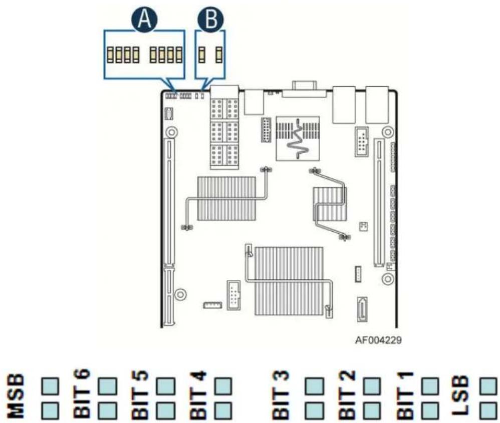
Figure 60. Diagnostic LED Placement Diagram (Block A)
In the following example, the BIOS sends a value of ACh to the diagnostic LED decoder. The LEDs are decoded as follows.
Table 106. POST Progress Code LED Example
| LEDs | Upper Nibble LEDs | Lower Nibble LEDs | ||||||
| MSB | LSB | |||||||
| LED #7 | LED #6 | LED #5 | LED #4 | LED #3 | LED #2 | LED #1 | LED #0 | |
| 8h | 4h | 2h | 1h | 8h | 4h | 2h | 1h | |
| Status | ON | OFF | ON | OFF | ON | ON | OFF | OFF |
| Results | 1 | 0 | 1 | 0 | 1 | 1 | 0 | 0 |
| Ah | Ch | |||||||
Upper nibble bits = 1010b = Ah; Lower nibble bits = 1100b = Ch; the two are concatenated as ACh.
Table 107. Diagnostic LED POST Code Decoder
| Progress Code | Description |
| SEC Phase | |
| 0x01 | First POST code after CPU reset |
| 0x02 | Microcode load begin |
| 0x03 | CRAM initialization begin |
| 0x04 | Pei Cache When Disabled |
| 0x05 | SEC Core At Power On Begin |
| 0x06 | Early CPU initialization during Sec Phase |
| 0x07 | Early SB initialization during Sec Phase |
| 0x08 | Early NB initialization during Sec Phase |
| 0x09 | End Of Sec Phase |
| 0x0E | Microcode Not Found |
| 0x0F | Microcode Not Loaded |
| PEI Phase | |
| 0x10 | PEI Core |
| 0x11 | CPU PEIM |
| 0x15 | NB PEIM |
| 0x19 | SB PEIM |
| MRC Progress CodesAt this point the MRC Progress Code sequence is executed | |
| 0x31 | Memory Installed |
| 0x32 | CPU PEIM (CPU Init) |
| 0x33 | CPU PEIM (Cache Init) |
| 0x34 | CPU PEIM (BSP Select) |
| 0x35 | CPU PEIM (AP Init) |
| 0x36 | CPU PEIM (CPU SMM Init) |
| 0x4F | Dxe IPL started |
| DXE Phase | |
| 0x60 | DXE Core started |
| 0x61 | DXE NVRAM Init |
| 0x62 | SB RUN Init |
| 0x63 | DXE CPU Init |
| 0x68 | DXE PCI Host Bridge Init |
| 0x69 | DXE NB Init |
| 0x6A | DXE NB SMM Init |
| 0x70 | DXE SB Init |
| 0x71 | DXE SB SMM Init |
| 0x72 | DXE SB devices Init |
| 0x78 | DXE ACPI Init |
| 0x79 | DXE CSM Init |
| 0x90 | DXE BDS Started |
| 0x91 | DXE BDS connect drivers |
| 0x92 | DXE PCI Bus begin |
| 0x93 | DXE PCI Bus HPC Init |
| 0x94 | DXE PCI Bus enumeration |
| 0x95 | DXE PCI Bus resource requested |
| 0x96 | DXE PCI Bus assign resource |
| 0x97 | DXE CON_OUT connect |
| 0x98 | DXE CON_IN connect |
| 0x99 | DXE SIO Init |
| 0x9A | DXE USB start |
| 0x9B | DXE USB reset |
| 0x9C | DXE USB detect |
| 0x9D | DXE USB enable |
| 0xA1 | DXE IDE begin |
| 0xA2 | DXE IDE reset |
| 0xA3 | DXE IDE detect |
| 0xA4 | DXE IDE enable |
| 0xA5 | DXE SCSI begin |
| 0xA6 | DXE SCSI reset |
| 0xA7 | DXE SCSI detect |
| 0xA8 | DXE SCSI enable |
| 0xA9 | DXE verifying SETUP password |
| 0xAB | DXE SETUP start |
| 0xAC | DXE SETUP input wait |
| 0xAD | DXE Ready to Boot |
| 0xAE | DXE Legacy Boot |
| 0xAF | DXE Exit Boot Services |
| 0xB0 | RT Set Virtual Address Map Begin |
| 0xB1 | RT Set Virtual Address Map End |
| 0xB2 | DXE Legacy Option ROM init |
| 0xB3 | DXE Reset system |
| 0xB4 | DXE USB Hot plug |
| 0xB5 | DXE PCI BUS Hot plug |
| 0xB6 | DXE NVRAM cleanup |
| 0xB7 | DXE Configuration Reset |
| 0x00 | INT19 |
| S3 Resume | |
| 0xE0 | S3 Resume PEIM (S3 started) |
| 0xE1 | S3 Resume PEIM (S3 boot script) |
| 0xE2 | S3 Resume PEIM (S3 Video Repost) |
| 0xE3 | S3 Resume PEIM (S3 OS wake) |
| BIOS Recovery | |
| 0xF0 | PEIM which detected forced Recovery condition |
| 0xF1 | PEIM which detected User Recovery condition |
| 0xF2 | Recovery PEIM (Recovery started) |
| 0xF3 | Recovery PEIM (Capsule found) |
| 0xF4 | Recovery PEIM (Capsule loaded) |
Appendix F: Video POST Code Errors
The table below lists the supported POST Error Codes, with a descriptive Error Message text for each. There is also a Response listed, which classifies the error as Minor, Major, or Fatal depending on how serious the error is and what action the system should take.
The Response section in the following table indicates one of these actions:
Minor: The message is displayed on the screen or on the Error Manager screen, and an error is logged to the SEL. The system continues booting in a degraded state. The user may want to replace the erroneous unit. The POST Error Pause option setting in the BIOS setup does not have any effect on this error.
Major: The message is displayed on the Error Manager screen, and an error is logged to the SEL. The POST Error Pause option setting in the BIOS setup determines whether the system pauses to the Error Manager for this type of error so the user can take immediate corrective action or the system continues booting.
Note that for 0048 "Password check failed", the system halts, and then after the next reset/reboot will display the error code on the Error Manager screen.
Fatal: The system halts during post at a blank screen with the text “Unrecoverable fatal error found. System will not boot until the error is resolved” and “Press
When the operator presses the F2 key on the keyboard, the error message is displayed on the Error Manager screen, and an error is logged to the SEL with the error code. The system cannot boot unless the error is resolved. The user needs to replace the faulty part and restart the system.
Again, note that these Error Codes and the messages that go with them must be coordinated with the master list maintained by the Server Management Utilities team.
Be aware that the POST Error Code list shown in this table may contain error codes which do not necessarily apply uniformly to every platform. Only a subset of these error codes will be applicable to any given server board.
Table 108. POST Error Messages and Handling
| Error Code | Error Message | Response |
| 0012 | System RTC date/time not set | Major |
| 0048 | Password check failed | Major |
| 113 | Fixed media not detected | Major |
| 0140 | PCI component encountered a PERR error | Major |
| 0141 | PCI resource conflict | Major |
| 0146 | PCI out of resources error | Major |
| 0191 | Processor core/thread count mismatch detected | Fatal |
| 0192 | Processor cache size mismatch detected | Fatal |
| 0194 | Processor family mismatch detected | Fatal |
| 0195 | Processor Intel(R) QPI link frequencies unable to synchronize | Fatal |
| 0196 | Processor model mismatch detected | Fatal |
| 0197 | Processor frequencies unable to synchronize | Fatal |
| 5220 | BIOS Settings reset to default settings | Major |
| 5221 | Passwords cleared by jumper | Major |
| 5224 | Password clear jumper is Set | Major |
| 8130 | Processor 01 disabled | Major |
| 8131 | Processor 02 disabled | Major |
| 8132 | Processor 03 disabled | Major |
| 8133 | Processor 04 disabled | Major |
| 8160 | Processor 01 unable to apply microcode update | Major |
| 8161 | Processor 02 unable to apply microcode update | Major |
| 8162 | Processor 03 unable to apply microcode update | Major |
| 8163 | Processor 04 unable to apply microcode update | Major |
| 8170 | Processor 01 failed Self Test (BIST) | Major |
| 8171 | Processor 02 failed Self Test (BIST) | Major |
| 8172 | Processor 03 failed Self Test (BIST) | Major |
| 8173 | Processor 04 failed Self Test (BIST) | Major |
| 8180 | Processor 01 microcode update not found | Minor |
| 8181 | Processor 02 microcode update not found | Minor |
| 8182 | Processor 03 microcode update not found | Minor |
| 8183 | Processor 04 microcode update not found | Minor |
| 8190 | Watchdog timer failed on last boot | Major |
| 8198 | OS boot watchdog timer failure | Major |
| 8300 | Baseboard management controller failed self test | Major |
| 8305 | Hot Swap Controller failure | Major |
| 83A0 | Management Engine (ME) failed self test | Major |
| 83A1 | Management Engine (ME) Failed to respond. | Major |
| 84F2 | Baseboard management controller failed to respond | Major |
| 84F3 | Baseboard management controller in update mode | Major |
| 84F4 | Sensor data record empty | Major |
| 84FF | System event log full | Minor |
| 8500 | Memory component could not be configured in the selected RAS mode | Major |
| 8501 | DIMM Population Error | Major |
| 8520 | DIMM_A1 failed test/initialization | Major |
| 8521 | DIMM_A2 failed test/initialization | Major |
| 8522 | DIMM_A3 failed test/initialization | Major |
| 8523 | DIMM_B1 failed test/initialization | Major |
| 8524 | DIMM_B2 failed test/initialization | Major |
| 8525 | DIMM_B3 failed test/initialization | Major |
| 8526 | DIMM_C1 failed test/initialization | Major |
| 8527 | DIMM_C2 failed test/initialization | Major |
| 8528 | DIMM_C3 failed test/initialization | Major |
| 8529 | DIMM_D1 failed test/initialization | Major |
| 852A | DIMM_D2 failed test/initialization | Major |
| 852B | DIMM_D3 failed test/initialization | Major |
| 852C | DIMM_E1 failed test/initialization | Major |
| 852D | DIMM_E2 failed test/initialization | Major |
| 852E | DIMM_E3 failed test/initialization | Major |
| 852F | DIMM_F1 failed test/initialization | Major |
| 8530 | DIMM_F2 failed test/initialization | Major |
| 8531 | DIMM_F3 failed test/initialization | Major |
| 8532 | DIMM_G1 failed test/initialization | Major |
| 8533 | DIMM_G2 failed test/initialization | Major |
| 8534 | DIMM_G3 failed test/initialization | Major |
| 8535 | DIMM_H1 failed test/initialization | Major |
| 8536 | DIMM_H2 failed test/initialization | Major |
| 8537 | DIMM_H3 failed test/initialization | Major |
| 8538 | DIMM_J1 failed test/initialization | Major |
| 8539 | DIMM_J2 failed test/initialization | Major |
| 853A | DIMM_J3 failed test/initialization | Major |
| 853B | DIMM_K1 failed test/initialization | Major |
| 853C | DIMM_K2 failed test/initialization | Major |
| 853D | DIMM_K3 failed test/initialization | Major |
| 853E | DIMM_L1 failed test/initialization | Major |
| 853F(Go to 85C0) | DIMM_L2 failed test/initialization | Major |
| 8540 | DIMM_A1 disabled | Major |
| 8541 | DIMM_A2 disabled | Major |
| 8542 | DIMM_A3 disabled | Major |
| 8543 | DIMM_B1 disabled | Major |
| 8544 | DIMM_B2 disabled | Major |
| 8545 | DIMM_B3 disabled | Major |
| 8546 | DIMM_C1 disabled | Major |
| 8547 | DIMM_C2 disabled | Major |
| 8548 | DIMM_C3 disabled | Major |
| 8549 | DIMM_D1 disabled | Major |
| 854A | DIMM_D2 disabled | Major |
| 854B | DIMM_D3 disabled | Major |
| 854C | DIMM_E1 disabled | Major |
| 854D | DIMM_E2 disabled | Major |
| 854E | DIMM_E3 disabled | Major |
| 854F | DIMM_F1 disabled | Major |
| 8550 | DIMM_F2 disabled | Major |
| 8551 | DIMM_F3 disabled | Major |
| 8552 | DIMM_G1 disabled | Major |
| 8553 | DIMM_G2 disabled | Major |
| 8554 | DIMM_G3 disabled | Major |
| 8555 | DIMM_H1 disabled | Major |
| 8556 | DIMM_H2 disabled | Major |
| 8557 | DIMM_H3 disabled | Major |
| 8558 | DIMM_J1 disabled | Major |
| 8559 | DIMM_J2 disabled | Major |
| 855A | DIMM_J3 disabled | Major |
| 855B | DIMM_K1 disabled | Major |
| 855C | DIMM_K2 disabled | Major |
| 855D | DIMM_K3 disabled | Major |
| 855E | DIMM_L1 disabled | Major |
| 855F(Go to 85D0) | DIMM_L2 disabled | Major |
| 8560 | DIMM_A1 encountered a Serial Presence Detection (SPD) failure | Major |
| 8561 | DIMM_A2 encountered a Serial Presence Detection (SPD) failure | Major |
| 8562 | DIMM_A3 encountered a Serial Presence Detection (SPD) failure | Major |
| 8563 | DIMM_B1 encountered a Serial Presence Detection (SPD) failure | Major |
| 8564 | DIMM_B2 encountered a Serial Presence Detection (SPD) failure | Major |
| 8565 | DIMM_B3 encountered a Serial Presence Detection (SPD) failure | Major |
| 8566 | DIMM_C1 encountered a Serial Presence Detection (SPD) failure | Major |
| 8567 | DIMM_C2 encountered a Serial Presence Detection (SPD) failure | Major |
| 8568 | DIMM_C3 encountered a Serial Presence Detection (SPD) failure | Major |
| 8569 | DIMM_D1 encountered a Serial Presence Detection (SPD) failure | Major |
| 856A | DIMM_D2 encountered a Serial Presence Detection (SPD) failure | Major |
| 856B | DIMM_D3 encountered a Serial Presence Detection (SPD) failure | Major |
| 856C | DIMM_E1 encountered a Serial Presence Detection (SPD) failure | Major |
| 856D | DIMM_E2 encountered a Serial Presence Detection (SPD) failure | Major |
| 856E | DIMM_E3 encountered a Serial Presence Detection (SPD) failure | Major |
| 856F | DIMM_F1 encountered a Serial Presence Detection (SPD) failure | Major |
| 8570 | DIMM_F2 encountered a Serial Presence Detection (SPD) failure | Major |
| 8571 | DIMM_F3 encountered a Serial Presence Detection (SPD) failure | Major |
| 8572 | DIMM_G1 encountered a Serial Presence Detection (SPD) failure | Major |
| 8573 | DIMM_G2 encountered a Serial Presence Detection (SPD) failure | Major |
| 8574 | DIMM_G3 encountered a Serial Presence Detection (SPD) failure | Major |
| 8575 | DIMM_H1 encountered a Serial Presence Detection (SPD) failure | Major |
| 8576 | DIMM_H2 encountered a Serial Presence Detection (SPD) failure | Major |
| 8577 | DIMM_H3 encountered a Serial Presence Detection (SPD) failure | Major |
| 8578 | DIMM_J1 encountered a Serial Presence Detection (SPD) failure | Major |
| 8579 | DIMM_J2 encountered a Serial Presence Detection (SPD) failure | Major |
| 857A | DIMM_J3 encountered a Serial Presence Detection (SPD) failure | Major |
| 857B | DIMM_K1 encountered a Serial Presence Detection (SPD) failure | Major |
| 857C | DIMM_K2 encountered a Serial Presence Detection (SPD) failure | Major |
| 857D | DIMM_K3 encountered a Serial Presence Detection (SPD) failure | Major |
| 857E | DIMM_L1 encountered a Serial Presence Detection (SPD) failure | Major |
| 857F(Go to 85E0) | DIMM_L2 encountered a Serial Presence Detection (SPD) failure | Major |
| 85C0 | DIMM_L3 failed test/initialization | Major |
| 85C1 | DIMM_M1 failed test/initialization | Major |
| 85C2 | DIMM_M2 failed test/initialization | Major |
| 85C3 | DIMM_M3 failed test/initialization | Major |
| 85C4 | DIMM_N1 failed test/initialization | Major |
| 85C5 | DIMM_N2 failed test/initialization | Major |
| 85C6 | DIMM_N3 failed test/initialization | Major |
| 85C7 | DIMM_P1 failed test/initialization | Major |
| 85C8 | DIMM_P2 failed test/initialization | Major |
| 85C9 | DIMM_P3 failed test/initialization | Major |
| 85CA | DIMM_R1 failed test/initialization | Major |
| 85CB | DIMM_R2 failed test/initialization | Major |
| 85CC | DIMM_R3 failed test/initialization | Major |
| 85CD | DIMM_T1 failed test/initialization | Major |
| 85CE | DIMM_T2 failed test/initialization | Major |
| 85CF | DIMM_T3 failed test/initialization | Major |
| 85D0 | DIMM_L3 disabled | Major |
| 85D1 | DIMM_M1 disabled | Major |
| 85D2 | DIMM_M2 disabled | Major |
| 85D3 | DIMM_M3 disabled | Major |
| 85D4 | DIMM_N1 disabled | Major |
| 85D5 | DIMM_N2 disabled | Major |
| 85D6 | DIMM_N3 disabled | Major |
| 85D7 | DIMM_P1 disabled | Major |
| 85D8 | DIMM_P2 disabled | Major |
| 85D9 | DIMM_P3 disabled | Major |
| 85DA | DIMM_R1 disabled | Major |
| 85DB | DIMM_R2 disabled | Major |
| 85DC | DIMM_R3 disabled | Major |
| 85DD | DIMM_T1 disabled | Major |
| 85DE | DIMM_T2 disabled | Major |
| 85DF | DIMM_T3 disabled | Major |
| 85E0 | DIMM_L3 encountered a Serial Presence Detection (SPD) failure | Major |
| 85E1 | DIMM_M1 encountered a Serial Presence Detection (SPD) failure | Major |
| 85E2 | DIMM_M2 encountered a Serial Presence Detection (SPD) failure | Major |
| 85E3 | DIMM_M3 encountered a Serial Presence Detection (SPD) failure | Major |
| 85E4 | DIMM_N1 encountered a Serial Presence Detection (SPD) failure | Major |
| 85E5 | DIMM_N2 encountered a Serial Presence Detection (SPD) failure | Major |
| 85E6 | DIMM_N3 encountered a Serial Presence Detection (SPD) failure | Major |
| 85E7 | DIMM_P1 encountered a Serial Presence Detection (SPD) failure | Major |
| 85E8 | DIMM_P2 encountered a Serial Presence Detection (SPD) failure | Major |
| 85E9 | DIMM_P3 encountered a Serial Presence Detection (SPD) failure | Major |
| 85EA | DIMM_R1 encountered a Serial Presence Detection (SPD) failure | Major |
| 85EB | DIMM_R2 encountered a Serial Presence Detection (SPD) failure | Major |
| 85EC | DIMM_R3 encountered a Serial Presence Detection (SPD) failure | Major |
| 85ED | DIMM_T1 encountered a Serial Presence Detection (SPD) failure | Major |
| 85EE | DIMM_T2 encountered a Serial Presence Detection (SPD) failure | Major |
| 85EF | DIMM_T3 encountered a Serial Presence Detection (SPD) failure | Major |
| 8604 | POST Reclaim of non-critical NVRAM variables | Minor |
| 8605 | BIOS Settings are corrupted | Major |
| 8606 | NVRAM variable space was corrupted and has been reinitialized | Major |
| 92A3 | Serial port component was not detected | Major |
| 92A9 | Serial port component encountered a resource conflict error | Major |
| 9505 | ATA/ATAPI interface error | Major |
| A000 | TPM device not detected. | Minor |
| A001 | TPM device missing or not responding. | Minor |
| A002 | TPM device failure. | Minor |
| A003 | TPM device failed self test. | Minor |
| A100 | BIOS ACM Error | Major |
| A421 | PCI component encountered a SERR error | Fatal |
| A5A0 | PCI Express component encountered a PERR error | Minor |
| A5A1 | PCI Express component encountered an SERR error | Fatal |
| A6A0 | DXE Boot Services driver: Not enough memory available to shadow a Legacy Option ROM. | Minor |
Glossary
This glossary contains important terms used in the preceding chapters. For ease of use, numeric entries are listed first (for example, 82460GX) with alpha entries following (for example, AGP 4x). Acronyms are then entered in their respective place, with non-acronyms following.
Table 109. Glossary
| Term | Definition |
| ACPI | Advanced Configuration and Power Interface |
| AP | Application Processor |
| APIC | Advanced Programmable Interrupt Control |
| ARP | Address Resolution Protocol |
| ASIC | Application Specific Integrated Circuit |
| BIOS | Basic Input/Output System |
| BIST | Built-In Self Test |
| BMC | Baseboard Management Controller |
| Bridge | Circuitry connecting one computer bus to another, allowing an agent on one to access the other |
| BSP | Bootstrap Processor |
| Byte | 8-bit quantity. |
| CATERR | On a catastrophic hardware event the core signals CATERR to the uncore. The core enters a halted state that can only be exited by a reset. |
| CBC | Chassis Bridge Controller (A microcontroller connected to one or more other CBCs, together they bridge the IPMB buses of multiple chassis.) |
| CEK | Common Enabling Kit |
| CHAP | Challenge Handshake Authentication Protocol |
| CMOS | In terms of this specification, this describes the PC-AT compatible region of battery-backed 128 bytes of memory, which normally resides on the server board. |
| DCMI | Data Center Management Interface |
| DHCP | Dynamic Host Configuration Protocol |
| DPC | Direct Platform Control |
| EEPROM | Electrically Erasable Programmable Read-Only Memory |
| EHCI | Enhanced Host Controller Interface |
| EMP | Emergency Management Port |
| EPS | External Product Specification |
| FBD | Fully Buffered DIMM |
| FMB | Flexible Mother Board |
| FRB | Fault Resilient Booting |
| FRU | Field Replaceable Unit |
| FSB | Front Side Bus |
| GB | 1024 MB |
| GPIO | General Purpose I/O |
| GTL | Gunning Transceiver Logic |
| GPA | Guest Physical Address |
| HSC | Hot-Swap Controller |
| HPA | Host Physical Address |
| Hz | Hertz (1 cycle/second) |
| I^2C | Inter-Integrated Circuit Bus |
| IA | Intel® Architecture |
| IBF | Input Buffer |
| ICH | I/O Controller Hub |
| IC MB | Intelligent Chassis Management Bus |
| IFB | I/O and Firmware Bridge |
| ILM | Independent Loading Mechanism |
| IMC | Integrated Memory Controller |
| INTR | Interrupt |
| IP | Internet Protocol |
| IPMB | Intelligent Platform Management Bus |
| IPMI | Intelligent Platform Management Interface |
| IR | Infrared |
| ITP | In-Target Probe |
| KB | 1024 bytes |
| KCS | Keyboard Controller Style |
| LAN | Local Area Network |
| LCD | Liquid Crystal Display |
| LED | Light Emitting Diode |
| LPC | Low Pin Count |
| LSB | Least Significant Bit |
| LUN | Logical Unit Number |
| MAC | Media Access Control |
| MB | 1024KB |
| ME | Management Engine |
| MD2 | Message Digest 2 – Hashing Algorithm |
| MD5 | Message Digest 5 – Hashing Algorithm – Higher Security |
| ms | Milliseconds |
| MSB | Most Significant Bit |
| MTTR | Memory Type Range Register |
| Mux | Multiplexor |
| NIC | Network Interface Controller |
| NMI | Nonmaskable Interrupt |
| OBF | Output Buffer |
| OEM | Original Equipment Manufacturer |
| Ohm | Unit of electrical resistance |
| PECI | Platform Environment Control Interface |
| PEF | Platform Event Filtering |
| PEP | Platform Event Paging |
| PIA | Platform Information Area (This feature configures the firmware for the platform hardware) |
| PLD | Programmable Logic Device |
| PMI | Platform Management Interrupt |
| POST | Power-On Self Test |
| PSMI | Power Supply Management Interface |
| PWM | Pulse-Width Modulation |
| QPI | QuickPath Interconnect |
| RAM | Random Access Memory |
| RASUM | Reliability, Availability, Serviceability, Usability, and Manageability |
| RISC | Reduced Instruction Set Computing |
| ROM | Read Only Memory |
| RTC | Real-Time Clock (Component of ICH peripheral chip on the server board) |
| RMM3 | Remote Management Module 3 |
| SDR | Sensor Data Record |
| SECC | Single Edge Connector Cartridge |
| SEEPROM | Serial Electrically Erasable Programmable Read-Only Memory |
| SEL | System Event Log |
| SIO | Server Input/Output |
| SMBus* | System Management BUS |
| SMI | Server Management Interrupt (SMI is the highest priority nonmaskable interrupt) |
| SMM | Server Management Mode |
| SMS | Server Management Software |
| SNMP | Simple Network Management Protocol |
| TBD | To Be Determined |
| TDP | Thermal Design Power |
| TIM | Thermal Interface Material |
| UART | Universal Asynchronous Receiver/Transmitter |
| UDP | User Datagram Protocol |
| UHCI | Universal Host Controller Interface |
| URS | Unified Retention System |
| UTC | Universal time coordinare |
| UUID | Universally Unique Identifier |
| VID | Voltage Identification |
| VLSI | Very Large Scale Integration |
| VRD | Voltage Regulator Down |
| VT | Virtualization Technology |
| Word | 16-bit quantity |
| ZIF | Zero Insertion Force |
Reference Documents
■ ACPI 3.0: http://www.acpi.info/spec.htm
■ IPMI 2.0
- Data Center Management Interface Specification v1.0, May 1, 2008: www.intel.com/go/dcmi
- PCI Bus Power Management Interface Specification 1.1: http://www.pcisig.com/
■ PCI Express* Base Specification Rev 2.0 Dec 06: http://www.pcisig.com/
- PCI Express* Card Electromechanical Specification Rev 2.0: http://www.pcisig.com/
■ PMBus*: http://pmbus.org
■ SATA 2.6: http://www.sata-io.org/
- SMBIOS 2.4
■ SSI-EEB 3.0: http://www.ssiforum.org
USB 1.1: http://www.usb.org
USB 2.0: http://www.usb.org
- Windows* Logo/SDG 3.0
Intel ^® Dynamic PowerTechnology Node Manager 1.5 External Interface Specification using IPMI, 2007. Intel Corporation.
- Node Power and Thermal Management Architecture Specification v1.5, rev.0.79. 2007, Intel Corporation.
Intel ^® Server System Integrated Baseboard Management Controller Core External Product Specification, 2007 Intel Corporation.
Intel ^® Thurley Server Platform Services IPMI Commands Specification, 2007. Intel Corporation.
Intel ^® Server Safety and Regulatory, 2011. Intel Corporation. Intel ^® order number: G31608-006.
- Intelligent Platform Management Bus Communications Protocol Specification, Version 1.0, 1998. Intel Corporation, Hewlett-Packard* Company, NEC* Corporation, Dell* Computer Corporation.
- Platform Environmental Control Interface (PECI) Specification, Version 2.0. Intel Corporation.
- Platform Management FRU Information Storage Definition, Version 1.0, Revision 1.2, 2002. Intel Corporation, Hewlett-Packard* Company, NEC* Corporation, Dell* Computer Corporation. http://developer.intel.com/design/servers/ipmi/spec.htm.
- Technical Product Specification
- Disclaimers
- Table of Contents
- Introduction .... 1
- Server Board Overview ....3
- Product Architecture Overview ....8
- Platform Management Functional Overview....39
- List of Figures
- List of Tables
- Introduction
- Section Outline
- Server Board Use Disclaimer
- Server Board Overview
- Server Board Connector and Component Layout
- Board Rear Connector Placement
- Server Board Mechanical Drawings
- Product Architecture Overview
- High Level Product Features
- Processor Support
- Processor Socket Assembly
- Processor Population Rules
- Processor Function Overview
- Processor Feature Details:
- Supported Technologies:
- Intel \* QuickPath Interconnect
- Integrated Memory Controller (IMC) and Memory Subsystem
- Supported Memory
- Notes:
- Memory Population Rules
- Publishing System Memory
- RAS Features
- Independent Channel Mode
- Rank Sparing Mode
- Mirrored Channel Mode
- Lockstep Channel Mode
- Processor Intergrated I/O Module (I/O)
- Riser Card Support
- Riser Types
- Network Interface
- I/O Module Support
- Intel °C600-A/B PCH Functional Overview
- PCI Express\*
- Non-Transparent Bridge
- Universal Serial Bus (USB)
- Serial Attached SCSI (SAS) and Serial ATA (SATA) Controller
- Note:
- PCI Interface
- Low Pin Count (LPC) Interface
- Digital Media Interface (DMI)
- Serials Peripheral Interface (SPI)
- Compatibility Modules (DMA Controller, Timer/Counters, Interrupt Controller)
- Advanced Programmable Interrupt Controller (APIC)
- Real Time Clock (RTC)
- GPIO
- Enhanced Power Management
- Fan Speed Control
- Intel \*Virtualization Technology for Direct I/O (Intel\* VT-d)
- KVM/Serial Over LAN (SOL) Function
- IDE-R Function
- Manageability
- System Management Bus (SMBus 2.0\*)
- Network Interface Controller (NIC)
- MAC Address Definition
- LAN Manageability
- Wake-On-LAN
- LAN Connector Ordering
- Thermal Sensor
- InfiniBand\* Controller
- Device Interfaces
- Quad Small Form-factor Pluggable (QSFP) Connector
- Integrated Baseboard Management Controller Overview
- Super I/O Controller
- Keyboard and Mouse Support
- Wake-up Control
- Graphics Controller and Video Support
- Remote KVM
- Platform Management Functional Overview
- Baseboard Management Controller (BMC) Firmware Feature Support
- IPMI 2.0 Features
- Non-IPMI Features
- New Manageability Features
- Advanced Configuration and Power Interface (ACPI)
- Platform Management SMBus\* and I 2 C Implementation
- BMC Internal Timestamp Clock
- Sensor Monitoring
- Messaging Interfaces
- Channel Management
- User Model
- Sessions
- BMC LAN Channels
- Baseboard NICs
- Dedicated Management Channel
- Concurrent Server Management Use of Multiple Ethernet Controllers
- IPv6 Support
- LAN Failover
- BMC IP Address Configuration
- Static IP Address (IP Address Source Value 0h, 1h, and 3h)
- Enabling/Disableing Dynamic Host Configuration Protocol (DHCP)
- DHCP BMC Hostname
- Address Resolution Protocol (ARP)
- Virtual Local Area Network (VLAN)
- Secure Shell (SSH)
- Serial-over-LAN (SOL 2.0)
- Platform Event Filter (PEF)
- LAN Alerting
- SNMP Platform Event Traps (PETs)
- Alert Policy Table
- Email Alerting
- SM-CLP (SM-CLP Lite)
- System Event Log (SEL)
- Servicing Events
- SEL Entry Deletion
- SEL Erasure
- SEL Extension Capabilities
- Sensor Data Record (SDR) Repository
- Field Replaceable Unit (FRU) Inventory Device
- Diagnostics and Beep Code Generation
- Diagnostics Interrupt (NMI)
- BMC Basic and Advanced Management Features
- Enabling Advanced Manageability Features
- Keyboard, Video, and Mouse (KVM) Redirection
- Remote Console
- Performance
- Security
- Availability
- Timeout
- Usage
- Media Redirection
- Availability
- Network Port Usage
- Embedded Web Server
- Data Center Management Interface (DCMI)
- Local Directory Authentication Protocol (LDAP)
- Platform/Chassis Management
- Thermal Control
- Fan Speed Control Profiles
- System Configuration Using FRUSDR Utility
- Node Power On/Off Control
- Intel® Intelligent Power Node Manager
- Overview
- Features
- Management Engine (ME)
- Overview
- BMC - Management Engine (ME) Distributed Model
- ME System Management Bus (SMBus\*) Interface
- BMC - Management Engine Interaction
- ME Power and Firmware Startup
- SmaRT/CLST
- Other Platform Management
- Wake On LAN (WOL)
- PCI Express\* Power Management
- PMBus\*
- Node Power Policies
- BIOS Setup Interface
- HotKeys Supported during POST
- POST Logo/Diagnostic Screen
- BIOS Boot Pop-up Menu
- BIOS Setup Utility
- BIOS Setup Operation
- Setup Page Layout
- Entering BIOS Setup
- Setup Navigation Keyboard Commands
- Setup Screen Menu Selection Bar
- BIOS Setup Utility Screens
- Map of Screens and Functionality
- Main Screen (Tab)
- Advanced Screen (Tab)
- Processor Configuration
- Advanced
- Power and Performance Policy
- Memory Configuration
- Memory Configuration
- ▶ Memory RAS and Performance Configuration
- DIMM Information
- Memory RAS and Performance Configuration
- Mass Storage Controller Configuration
- PCI Configuration
- NIC Configuration
- NIC Configuration
- UEFI Network Stack
- UEFI Option ROM Control
- i350 Gigabit Network Connection
- Processor PCIe Link Speed Configuration
- Serial Port Configuration
- USB Configuration
- System Acoustic and Performance Configuration
- Security Screen (Tab)
- Server Management Screen (Tab)
- Console Redirection
- System Information
- BMC LAN Configuration
- Boot Options Screen (Tab)
- CDROM Order
- Hard Disk Order
- Floppy Order
- Network Device Order
- BEV Device Order
- Boot Options
- Add EFI Boot Option
- Delete EFI Boot Option
- Boot Manager Screen (Tab)
- Error Manager Screen (Tab)
- Save and Exit Screen (Tab)
- Loading BIOS Defaults
- Configuration Jumpers
- Force Integrated BMC Update (J6B1)
- Force ME Update (J1E2)
- Password Clear (J1B6)
- BIOS Recovery Mode (J1E1)
- Reset BIOS Settings (J1D5)
- Connector/Header Locations and Pin-out
- Power Connectors
- System Management Headers
- Intel \*Remote Management Module 4 (Intel\* RMM4 Lite) Connector
- IPMB Header
- Bridge Board Connector
- Power Button
- Reset Button
- Chassis Identify Button
- Power LED
- System Status LED
- Chassis ID LED
- I/O Connectors
- PCI Express\* Connectors
- VGA Connector
- NIC Connectors
- SATA Connectors
- Hard Drive Activity (Input) LED Header
- Storage Upgrade Key Connector
- Serial Port Connectors
- USB Connectors
- QSFP for InfiniBand\*
- Fan Headers
- Chassis Intrusion
- Intel ® Light-Guided Diagnostics
- Front Panel Support
- System ID LED
- System Status LED
- Network Link/Activity LED
- Dedicated InfiniBand\* Link/Activity LED
- POST Code Diagnostic LEDs
- Environmental Limits Specification
- System Level Environmental Considerations
- Set Throttling Mode
- Altitude
- Set Fan Profile
- Fan PWM Offset
- Quiet Fan Idle Mode
- Thermal Sensor Input for Fan Speed Control
- Processor Thermal Design Power (TDP) Support
- Power Supply Specification Guidelines
- Power Supply DC Output Connector
- Power Supply DC Output Specification
- Output Power/Currents
- Standby Output
- Voltage Regulation
- Dynamic Loading
- Capacitive Loading
- Grounding
- Closed Loop Stability
- Residual Voltage Immunity in Standby Mode
- Common Mode Noise
- Soft Starting
- Zero Load Stability Requirements
- Hot Swap Requirements
- Forced Load Sharing
- Ripple/Noise
- Timing Requirement
- Appendix A: Integration and Usage Tips
- Appendix B: Integrated BMC Sensor Tables
- - Sensor Type
- ■ Event/Reading Type
- ■ Event Thresholds/Triggers
- - Assertion/Deassertion
- - Readable Value/Offsets
- - Event Data
- - Rearm Sensors
- - Default Hysteresis
- - Criticality
- - Standby
- Appendix C: BIOS Sensors and SEL Data
- Appendix D: Node Manager 2.0 IPMI Integrated Sensors
- Appendix E: POST Code LED Decoder
- Appendix F: Video POST Code Errors
- Glossary
- Reference Documents
Brand : INTEL
Model : HNS2600JFF
Category : Motherboard