
IDK-2119N-K2SXA2E - Screen Advantech - Free user manual and instructions
Find the device manual for free IDK-2119N-K2SXA2E Advantech in PDF.


| Product Type | Industrial LCD Monitor |
| Model | IDK-2119N-K2SXA2E |
| Brand | Advantech |
| Screen Size | 19 inches |
| Resolution | 1280 x 1024 (SXGA) |
| Aspect Ratio | 5:4 |
| Display Type | TFT LCD |
| Brightness | 300 cd/m² (typical) |
| Contrast Ratio | 1000:1 |
| Touchscreen | Not specified (likely optional) |
| Video Inputs | VGA, DVI-D |
| Power Supply | 12V DC |
| Power Consumption | Approx. 20W |
| Dimensions (W x H x D) | Approx. 430 x 350 x 50 mm |
| Weight | Approx. 5 kg |
| Mounting | VESA 100 x 100 mm |
| Operating Temperature | 0°C to 50°C |
| Storage Temperature | -20°C to 60°C |
| Usage | Industrial or commercial display |
| Maintenance | Clean with a soft, dry cloth |
| Safety | Use only with provided power adapter |
Frequently Asked Questions - IDK-2119N-K2SXA2E Advantech
User questions about IDK-2119N-K2SXA2E Advantech
0 question about this device. Answer the ones you know or ask your own.
Ask a new question about this device
Download the instructions for your Screen in PDF format for free! Find your manual IDK-2119N-K2SXA2E - Advantech and take your electronic device back in hand. On this page are published all the documents necessary for the use of your device. IDK-2119N-K2SXA2E by Advantech.
USER MANUAL IDK-2119N-K2SXA2E Advantech
natural_image
Illustration of four electronic circuit boards with white outlines on a purple background (no text or symbols)IDK-2119 Series
19" High Brightness SXGA LED-Backlight Display
Copyright
The documentation and software included with this product are copyrighted 2014 by Advantech Co., Ltd. All rights are reserved. Advantech Co., Ltd. reserves the right to improve the products described in this manual at any time without notice. No part of this manual may be reproduced, copied, translated or transmitted in any form or by any means without the prior written permission of Advantech Co., Ltd. Information provided in this manual is intended to be accurate and reliable. However, Advantech Co., Ltd. assumes no responsibility for its use, nor for any infringements of the rights of third parties that may result from its use.
Acknowledgements
AMI is a trademark of American Megatrends Inc.
IBM and PC are trademarks of International Business Machines Corporation.
Intel® Core 2 Quad, Pentium Dual-Core and Celeron are trademarks of Intel Corporation.
WinBond is a trademark of Winbond Corporation.
All other product names or trademarks are properties of their respective owners.
Part No. 2006211903 Edition 4
Printed in China March 2015
Message to the Customer
Advantech Customer Services
All Advantech products are built to the most precise specifications to ensure reliable performance in the harsh and demanding conditions typical of industrial environments. Regardless of whether your new Advantech equipment is destined for a laboratory or factory floor, you can be assured that your product will provide the reliability and ease of operation for which Advantech is renowned.
Your satisfaction is our primary concern. To ensure you receive the full benefit of our services, please follow the instructions in this guide.
Technical Support
We want you to experience the maximum performance of your products. Should you encounter technical difficulties, we are available to provide assistance. Answers to the most frequently asked questions are provided in the product documentation. Generally, these answers are more detailed than the information we can offer over the telephone. So please consult this manual first. If you still cannot find the answer, gather all the information or questions that apply to your problem, and with the product close at hand, contact your dealer.
Our dealers are well trained and ready to provide the support you need to get the most from your Advantech products. In fact, most of the problems reported are minor and easily resolved over the telephone.
In addition, free technical support from Advantech engineers is available during business hours. We are always ready to offer advice regarding application requirements or to provide specific information related to the installation and operation of any of our products.
Product Warranty (2 years)
Advantech warrants the original purchaser that all products will be free from defects in materials and workmanship for two years from the date of purchase.
This warranty does not apply to products that have been repaired or altered by persons other than repair personnel authorized by Advantech, or products subject to misuse, abuse, accidents or improper installation. Advantech assumes no liability under the terms of this warranty as a consequence of such events.
Because of Advantech's high quality-control standards and rigorous testing, most of our customers never need to use our repair service. If an Advantech product is defective, it will be repaired or replaced at no charge during the warranty period. For out-of-warranty repairs, customers are billed according to the cost of the replacement materials, service time and freight. Please consult your dealer for more details.
If you believe your product to be defective, please follow the steps listed below:
-
Collect all information regarding the problem encountered. (For example, CPU speed, Advantech products involved, other hardware and software used, etc.) Note anything abnormal and list any onscreen messages you encounter when the problem occurs.
-
Call your dealer and describe the problem. Please have your manual, product number, and related information readily available.
-
If your product is diagnosed as defective, obtain an RMA (return merchandise authorization) number from your dealer. This allows us to process your return more quickly.
-
Carefully pack the defective product, a completed Repair and Replacement Order Card and a proof of purchase date (such as a photocopy of your sales receipt) in a shippable container. Products returned without a proof of purchase date will not be eligible for our warranty service.
-
Write the RMA number clearly on the outside of the packaging before shipping the product prepaid to your dealer.
Contents
Chapter 1 Overview......1
1.1 General Description 2
1.2 Specifications.... 2
1.2.1 LCD Panel.... 2
1.2.2 LED Driver Board.... 2
1.2.3 Touchscreen (R series).... 2
1.2.4 Environment.... 2
1.3 Mechanical Characteristics ...... 3
1.3.1 IDK-2119N-K2SXA2E 3
1.3.2 IDK-2119R-K2SXA2E 5
1.4 Functional Block Diagram 7
Figure 1.1 Functional block diagram....7
1.5 Touchscreen Driver....7
1.6 Absolute Maximum Ratings 7
1.6.1 Absolute Ratings for TFT LCD Module.... 7
1.6.2 Absolute Ratings for Backlight Unit.... 7
1.6.3 Absolute Environmental Ratings....8
Chapter 2 Electrical Characteristics......9
2.1 Power Specifications.... 10
Table 2.1: Power Specifications ...... 10
2.2 Backlight Driving Conditions 10
Table 2.2: Backlight Driving Conditions.... 10
Chapter 3 Signal Characteristics......13
3.1 Pixel Format Image.... 14
3.2 Pin Description.... 14
Table 3.1: Pin Description 14
3.3 Input Data Format 16
3.4 Interface Timing 16
3.4.1 Timing Characteristics 16
Table 3.2: Timing Characteristics.... 16
3.4.2 Input Timing Diagram.... 17
3.5 Power ON/OFF Sequence 17
Chapter 4 Connector and Pin Assignment.....19
4.1 TFT LCD Module.... 20
4.1.1 Connectors.... 20
Table 4.1: Connectors ...... 20
4.1.2 Pin Assignment.... 20
Table 4.2: Pin Assignment.... 20
4.2 Backlight Unit 20
4.2.1 LED Light Bar Connector Signals 21
4.2.2 LED Driver Board.... 21
Table 4.3: Specifications 21
Table 4.4: Input Connector Pin Definition (CN4) 22
Table 4.5: Output Connector Pin Definition (CN1 and CN2)..... 22
Figure 4.1 Dimensions.... 22
Chapter 5 Touchscreen and Controller...... 23
5.1 Touchscreen (Optional: for IDK-2119R only).... 24
5.1.1 Touch Characteristics.... 24
5.1.2 Optical Characteristics.... 24
5.1.3 Environmental Characteristics.... 24
5.1.4 Mechanical Characteristics.... 24
5.1.5 Electronic Characteristics 24
5.1.6 General Specifications.... 25
5.2 Touch Controller (Optional: for IDK-2119R only).... 25
5.2.1 Touch Controller Characteristics 25
5.2.2 Pin Assignment and Description.... 26
Figure 5.1 Board-mounted header 27
5.2.3 Physical Dimensions.... 28
Appendix A Optical Characteristics...... 29
A.1 Optical Characteristics.... 30
Table A.1: Optical Characteristics 30
Appendix B Handling Precautions.... 33
B.1 Handling Precautions.... 34
Chapter 1
Overview
1.1 General Description
The Advantech IDK-2119 series is equipped with a 19" 1200 cd/m2 industrial-grade LCD display and LED driver board. This series is also available with various touch-screen options and enhancements, such as AR surface treatment and optical bonding solutions. The IDK-2119 series supports a high brightness of 1200 cd/m2 at the maximum power consumption of 29.61 W. Featuring a high level of brightness and wide operating temperature range, IDK-2119 provides superior sunlight readability and is ideal for both semi-outdoor and outdoor environments.
1.2 Specifications
1.2.1 LCD Panel
■ Display Size: 19" LED backlight panel
■ Resolution: 1280 x 1024
■ Viewing Angle (U / D / L / R): 80° / 80° / 85° / 85°
■ Brightness: 1200 cd/m ^2
■ Contrast Ratio: 1100:1
■ Response Time (ms): 5 ms
Colors: 16.7 M
Voltage: 5 V
■ Power Consumption: 30.19 W
■ Signal Interface: Two-channel LVDS
■ Weight: R series: 2800g (typical)
N series: 1700g (typical)
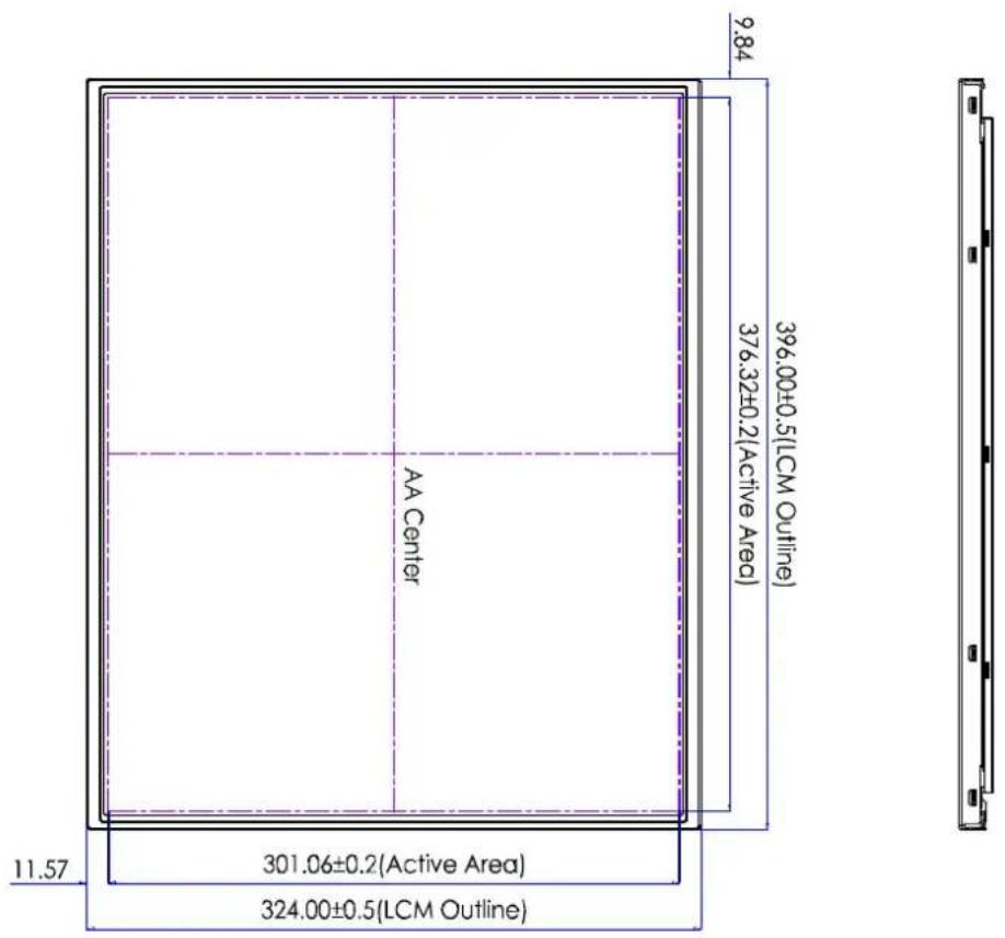
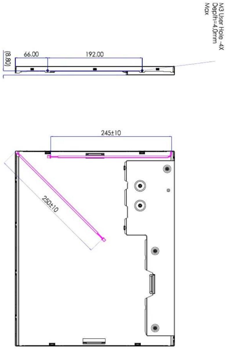
■ Dimensions (W x H x D): N series: 396 (H) x 324 (V) x 17.8 (D) (typical)
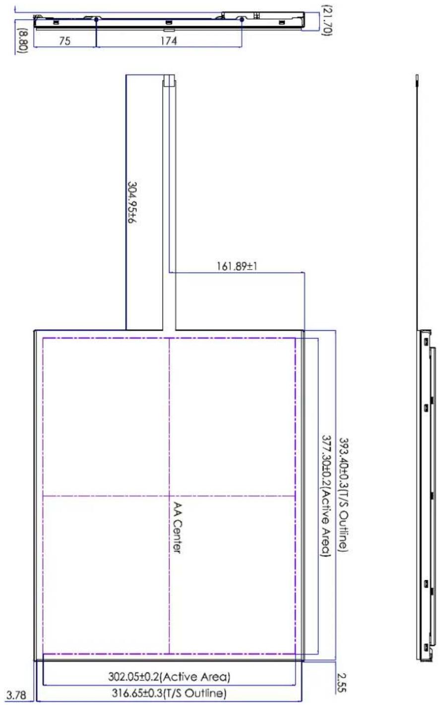
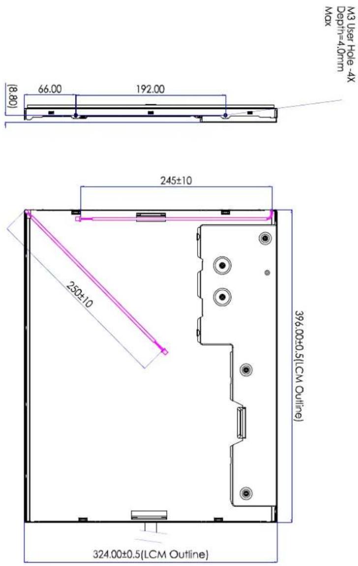
R series: 396 (H) x 324 (V) x 21.7 (D) (typical)
1.2.2 LED Driver Board
Efficiency: 92%
■ Output Current and Voltage: 1340 mA / 17.5 V (typical)
■ Dimensions (W x H x D): 80 x 54.2 x 16 mm
1.2.3 Touchscreen (R series)
■ Touchscreen: 5-wire resistive
■ Light Transmission: 80 ± 3%
■ Durability: x10 million
1.2.4 Environment
■ Operating Temperature: 0 \~ 50 °C
■ Storage Temperature: -20 \~ 60 °C
■ Humidity: 5 \~ 95% @ 40 °C, non-condensing
1.3 Mechanical Characteristics
1.3.1 IDK-2119N-K2SXA2E
Front View

Rear View
1.3.2 IDK-2119R-K2SXA2E
Front View
Rear View
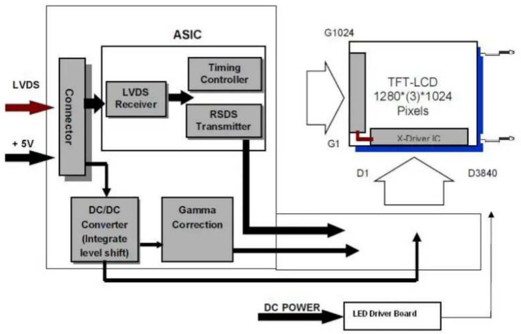
1.4 Functional Block Diagram
Below is a functional block diagram of the 19-inch color TFT-LCD module.
flowchart
graph TD
    A["LVDS"] --> B["Connector"]
    C["+5V"] --> B
    B --> D["LVDS Receiver"]
    D --> E["Timing Controller"]
    D --> F["RSDS Transmitter"]
    F --> G["Gamma Correction"]
    G --> H["DC/DC Converter (Integrate level shift)"]
    H --> I["DC POWER"]
    I --> J["LED Driver Board"]
    K["G1024"] --> L["TFT-LCD 1280*(3)*1024 Pixels"]
    L --> M["X-Driver IC"]
    M --> N["D3840"]
    N --> O["D1"]
    O --> P["G1"]
    P --> Q["ASIC"]
    Q --> R["DC/DC Converter (Integrate level shift)"]
    R --> G
Figure 1.1 Functional block diagram
1.5 Touchscreen Driver
Please download the touchscreen driver from www.advantech.com
1.6 Absolute Maximum Ratings
The absolute maximum allowable ratings for this module are as follows:
1.6.1 Absolute Ratings for TFT LCD Module
| Item Symbol Min. Max. Unit Conditions |
| Logic/LCD Drive Voltage VDD -0.3 +5.5 [Volt] Notes 1 and 2 |
1.6.2 Absolute Ratings for Backlight Unit
| Item Symbol Min. Max. Unit Conditions | ||||
| LED Light Bar Current | ILed | 670*2 | [mA] | Notes 1 and 2 |
1.6.3 Absolute Environmental Ratings
Item Symbol Min. Max. Unit Conditions
| Operating Temperature TOP 0 +50 [oC] | |||
| Operating Humidity HOP 8 90 [%RH] | |||
| Storage Temperature | TST | -20 | +60 [oC] |
| Storage Humidity | HST | 8 90 [%RH] | |
Note 1: Ta must not exceed 25 °C
Note 2: Permanent damage to the device may occur if the maximum values are exceeded.
Chapter 2
Electrical
Characteristics
2.1 Power Specifications
The input power specifications are as follows:
Table 2.1: Power Specifications
| Symbol | Parameter | Min. | Typ. | Max. | Unit | Condition |
| VCC Logic/LCD Drive Voltage | 4.5 5.0 5.5 [Volt] | ±10% | ||||
| ICC Input Current | -0.94 1.1 [A] Vin = 5.0 V; all white pattern; at 60 Hz | |||||
| PCC VCC Power | -4.7 5.5 [Watt] Vin = 5.0 V; all white pattern; at 60 Hz | |||||
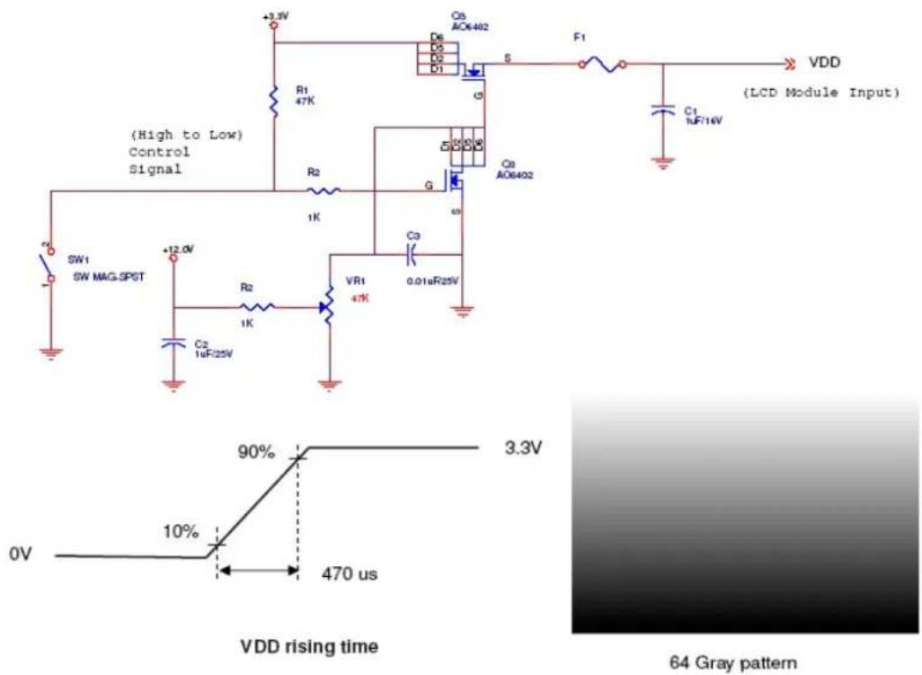
| IRush | Inrush Current | -2.1 | 2.5 [A] | Note 1 | ||
Note 1: Measurement condition
2.2 Backlight Driving Conditions
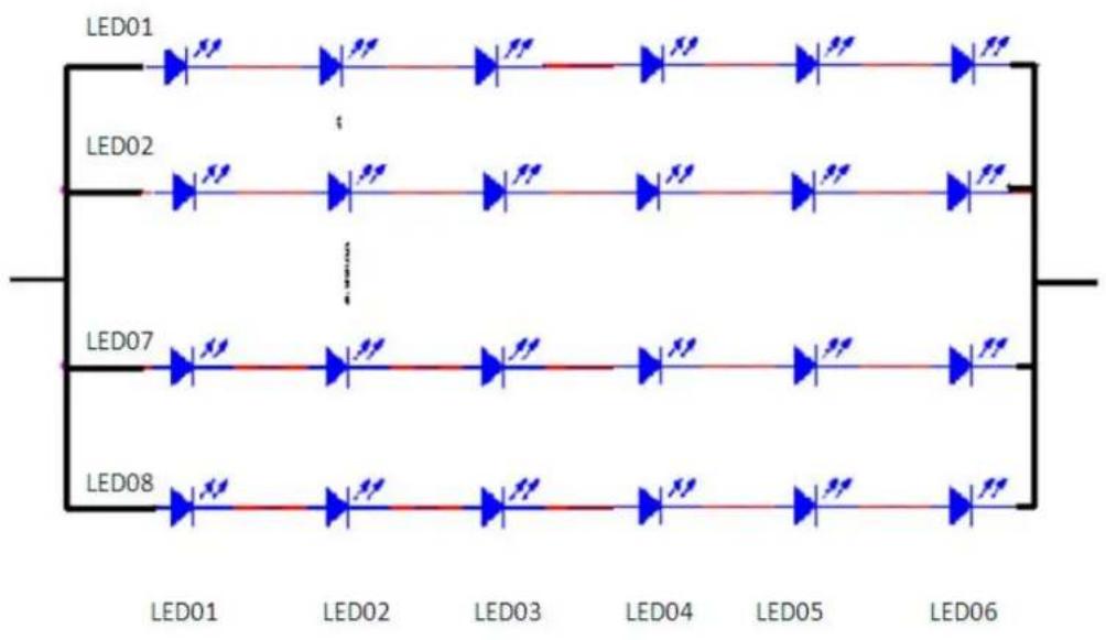
The parameter guideline of the LED light bar driver is 25 °C (room temperature) at stable condition.
Table 2.2: Backlight Driving Conditions
| Item | Symbol | Values | Unit | Condition | ||
| Min. | Typ. | Max. | ||||
| LED Voltage | VL | - | 17.5 | V | Notes 2 and 3 | |
| LED Current | IL | - | 670*2 | mA | Note 2 | |
| LED Lifetime | - | 50,000 | - | - | Hr | Note 1 |
Note 1: The LED lifetime is defined as the time before the module brightness decreases to 50% of the original brightness when at an ambient temperature of 25°C, with a typical LED current of 800 mA.
Note 2: The LED driving condition is defined for each LED module (6 LED serial).
Note 3: The variance in power consumed by the LED light bar is 10%. PLED is the calculated reference value (PLED = IL x VL x 2)
flowchart
graph TD
    A["LED01"] --> B["Switch"]
    C["LED02"] --> D["Switch"]
    E["LED07"] --> F["Switch"]
    G["LED08"] --> H["Switch"]
    B --> I["Diode 1"]
    D --> J["Diode 2"]
    F --> K["Diode 3"]
    H --> L["Diode 4"]
    I --> M["Diode 5"]
    J --> N["Diode 6"]
    K --> O["Diode 7"]
    L --> P["Diode 8"]
Chapter 3
Signal Characteristics
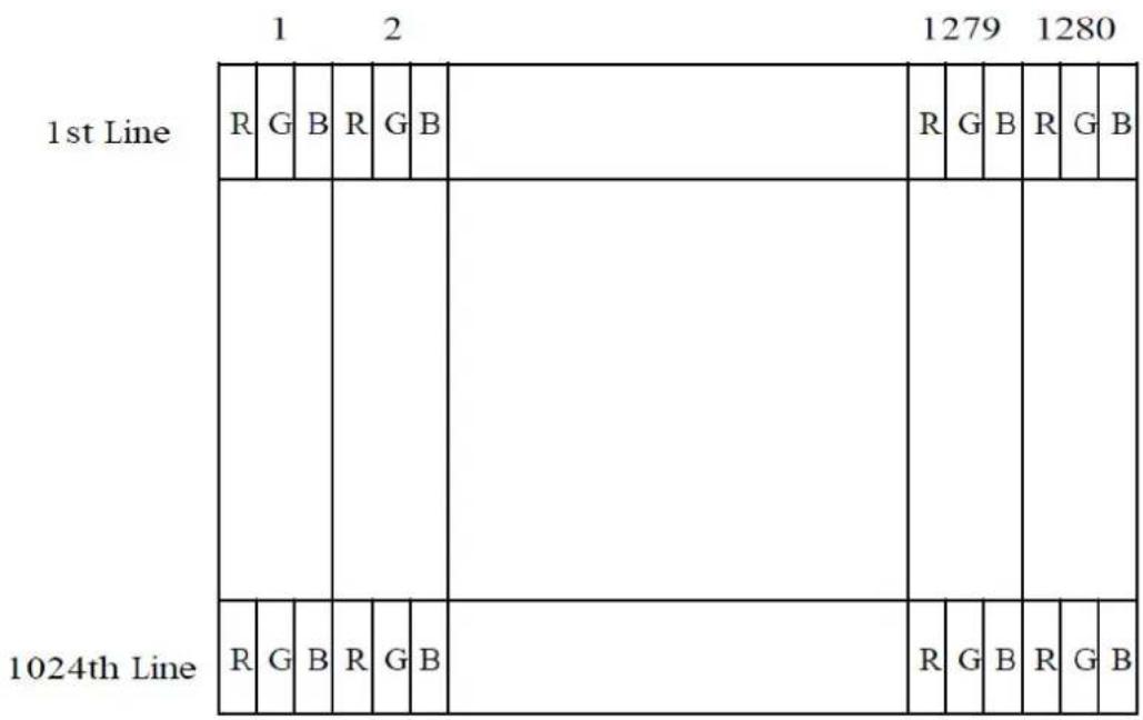
3.1 Pixel Format Image
The following figure shows the relationship between input signals and the LCD pixel format.
3.2 Pin Description
The module uses a pair of LVDS-compatible SN75LVDS82 receivers (Texas Instruments). LVDS is a differential signaling technology developed for LCD interfaces and high-speed data transfer devices. Additionally, the device transmitters are SN75LVDS83 compatible (negative edge sampling). The first LVDS port (RxOxxx) transmits odd pixels and the second LVDS port (RxExxx) transmits even pixels.
Table 3.1: Pin Description
| Pin No. Symbol Description | |
| 1 RxOIN0- Negative LVDS differential data input (odd data) | |
| 2 RxOIN0+ Positive LVDS differential data input (odd data) | |
| 3 RxOIN1- Negative LVDS differential data input (odd data) | |
| 4 RxOIN1+ Positive LVDS differential data input (odd data) | |
| 5 RxOIN2- Negative LVDS differential data input (odd data, H-Sync, V-Sync, DSPTMG) | |
| 6 RxOIN2+ Positive LVDS differential data input (odd data, H-Sync, V-Sync, DSPTMG) | |
| 7 VSS Power ground | |
| 8 RxOCLKIN- Negative LVDS differential clock input (odd clock) | |
| 9 RxOCLKIN+ Positive LVDS differential clock input (odd clock) | |
| 10 RxOIN3- Negative LVDS differential data input (odd data) | |
| 11 RxOIN3+ Positive LVDS differential data input (odd data) | |
| 12 RxEIN0- Negative LVDS differential data input (even data) | |
| 13 RxEIN0+ Positive LVDS differential data input (even data) | |
| 14 VSS Power ground |
Table 3.1: Pin Description
| 15 RxEIN1- Negative LVDS differential data input (even data) |
| 16 RxEIN1+ Positive LVDS differential data input (even data) |
| 17 VSS Power ground |
| 18 RxEIN2- Negative LVDS differential data input (even data) |
| 19 RxEIN2+ Positive LVDS differential data input (even data) |
| 20 RxECLKIN- Negative LVDS differential clock input (even clock) |
| 21 RxECLKIN+ Positive LVDS differential clock input (even clock) |
| 22 RxEIN3- Negative LVDS differential data input (even data) |
| 23 RxEIN3+ Positive LVDS differential data input (even data) |
| 24 VSS Power ground |
| 25 VSS Power ground |
| 26 NC No contact |
| 27 VSS Power ground |
| 28 VCC +5.0 V power supply |
| 29 VCC +5.0 V power supply |
| 30 VCC +5.0 V power supply |
3.3 Input Data Format
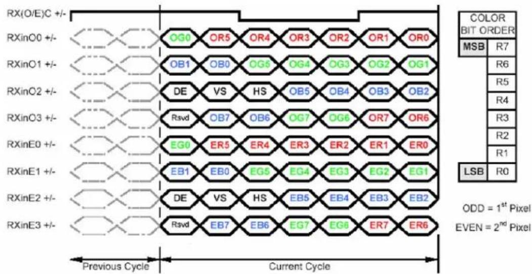
flowchart
graph TD
    A["RX(O/E)C +/-"] --> B["OG0 OR5 OR4 OR3 OR2 OR1 OR0"]
    A --> C["OB1 OB0 OG5 OG4 OG3 OG2 OG1"]
    A --> D["DE VS HS OB5 OB4 OB3 OB2"]
    A --> E["Rsvd OB7 OB6 OG7 OG6 OR7 OR6"]
    A --> F["EG0 ER5 ER4 ER3 ER2 ER1 ER0"]
    A --> G["EB1 EB0 EG5 EG4 EG3 EG2 EG1"]
    A --> H["DE VS HS EB5 EB4 EB3 EB2"]
    A --> I["Rsvd EB7 EB6 EG7 EG6 ER7 ER6"]
    J["RXinO0 +/-"] --> K["OG0 OR5 OR4 OR3 OR2 OR1 OR0"]
    J --> L["OB1 OB0 OG5 OG4 OG3 OG2 OG1"]
    J --> M["DE VS HS OB5 OB4 OB3 OB2"]
    N["RXinO1 +/-"] --> O["OG0 OR5 OR4 OR3 OR2 OR1 OR0"]
    N --> P["OB1 OB0 OG5 OG4 OG3 OG2 OG1"]
    N --> Q["DE VS HS OB5 EB4 EB3 EB2"]
    R["RXinO2 +/-"] --> S["OG0 OR5 OR4 OR3 OR2 OR1 OR0"]
    R --> T["OB1 OB0 OG5 OG4 OG3 OG2 OG1"]
    R --> U["DE VS HS EB5 EB4 EB3 EB2"]
    V["RXinO3 +/-"] --> W["OG0 OR5 OR4 OR3 OR2 OR1 OR0"]
    V --> X["OB1 OB0 OG5 OG4 OG3 OG2 OG1"]
    V --> Y["DE VS HS EB5 EB4 EB3 EB2"]
    Z["RXinE0 +/-"] --> AA["OG0 OR5 OR4 OR3 OR2 OR1 OR0"]
    Z --> AB["OB1 ER5 ER4 ER3 ER2 ER1 ER0"]
    Z --> AC["DE VS HS EB5 EB4 EB3 EB2"]
    AD["RXinE1 +/-"] --> AE["OG0 OR5 OR4 OR3 OR2 OR1 OR0"]
    AD --> AF["EB1 EB0 EG5 EG4 EG3 EG2 EG1"]
    AG["RXinE2 +/-"] --> AH["OG0 OR5 OR4 OR3 OR2 OR1 OR0"]
    AG --> AI["OB1 VS HS EB5 EB4 EB3 EB2"]
    AJ["RXinE3 +/-"] --> AK["OG0 OR5 OR4 OR3 OR2 OR1 OR0"]
    AJ --> AL["EB1 EB0 EG5 EG4 EG3 EG2 EG1"]
    AM["RXinO3 +/-"] --> AN["OG0 OR5 OR4 OR3 OR2 OR1 OR0"]
    AM --> AO["OB1 VS HS EB5 EB4 EB3 EB2"]
    AP["RXinE0 +/-"] --> AQ["OG0 OR5 OR4 OR3 OR2 OR1 OR0"]
    AP --> AR["EB1 EB0 EG5 EG4 EG3 EG2 EG1"]
    AS["RXinE1 +/-"] --> AT["OG0 OR5 OR4 OR3 OR2 OR1 OR0"]
    AS --> AU["OB1 VS HS EB5 EB4 EB3 EB2"]
    AV["RXinE2 +/-"] --> AW["OG0 OR5 OR4 OR3 OR2 OR1 OR0"]
    AV --> AX["EB1 EB0 EG5 EG4 EG3 EG2 EG1"]
    AY["RXinO0 +/-"] --> AZ["OG0 OR5 OR4 OR3 OR2 OR1 OR0"]
    BA["RXinO1 +/-"] --> BB["OB1 OB0 OG5 OG4 OG3 OG2 OG1"]
    BC["RXinO2 +/-"] --> BD["DE VS HS EB5 EB4 EB3 EB2"]
    BE["RXinO3 +/-"] --> BF["Rsvd OB7 OB6 OG7 OG6 OR7 OR6"]
    BG["RXinE0 +/-"] --> BH["EG0 ER5 ER4 ER3 ER2 ER1 ER0"]
    BI["RXinE1 +/-"] --> BJ["EB1 EB0 EG5 EG4 EG3 EG2 EG1"]
    BK["RXinE2 +/-"] --> BL["DE VS HS EB5 EB4 EB3 EB2"]
    BM["RXinE3 +/-"] --> BN["Rsvd EB7 EB6 EG7 EG6 ER7 ER6"]
Note 1: Typically, DE mode only. VS and HS on the EVEN channel are not used.
Note 2: Please follow VESA.
Note 3: 8-bit input
3.4 Interface Timing
3.4.1 Timing Characteristics
Table 3.2: Timing Characteristics
| Signal Item Symbol Min. Typ. Max. Unit | ||||||
| Vertical Section | Period TV | 1032 1066 1150 T | H | |||
| Active Tdisp(V) | 1024 1024 1024 T | H | ||||
| Blanking Tbp(V)+Tfp(V)+PWVS | 8 | 42 | 126 | TH | ||
| Horizontal Section | Period TH | 780 | 844 | 2047 T | Clock | |
| Active Tdisp(H) | 640 | 640 | 640 T | Clock | ||
| Blanking Tbp(H)+Tfp(H)+PWHS | 140 | 204 | - | TClock | ||
| Clock | Period TClock | 22.2 | 18.52 | 14.81 | ns | |
| Frequency Freq | 45 | 54 | 67.5 | MHz | ||
| Frame Rate | Frequency 1/TV | 50 | 60 | 75 | Hz | |
Note 1: DE mode
3.4.2 Input Timing Diagram
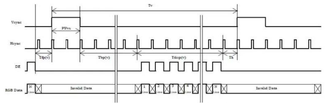
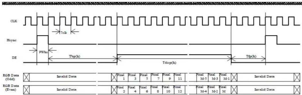
3.5 Power ON/OFF Sequence
The VDD power and lamp ON/OFF sequence, in addition to the interface signals, are shown below. Signals from any system should be in Hi-Z state or at a low level when the VDD is off.
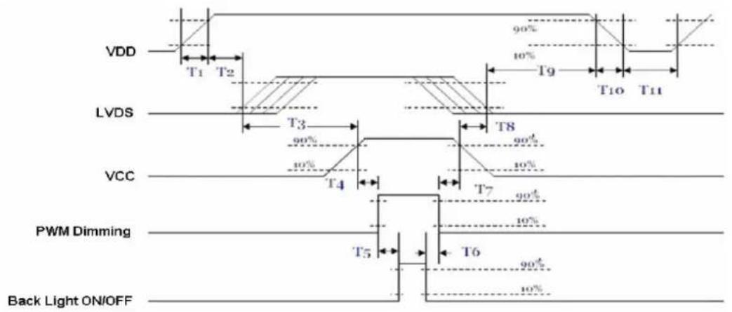
Power Sequence Timing
| Parameter | Value | Unit | ||
| Min. | Typ. | Max. | ||
| T1 | 0.5 | - | 10 | [ms] |
| T2 | 30 | 40 | 50 | [ms] |
| T3 | 175 | - | - | [ms] |
| T4 | 10 | - | - | [ms] |
| T5 | 10 | - | - | [ms] |
| T6 | 0 | - | - | [ms] |
| T7 | 10 | - | - | [ms] |
| T8 100 - - [ms] | ||||
| T9 0 16 50 [ms] | ||||
| T10 [ms] | ||||
| T11 1000 | [ms] | |||
Chapter 4
Connector and Pin Assignment
4.1 TFT LCD Module
The physical interface of the connectors on the TFT LCD module are described in this section. The components and signals accommodated by these connectors are as follows:
4.1.1 Connectors
| Table 4.1: Connectors | |
| Connector Name / Description Interface Connector / Interface Card | |
| Manufacturer JAE / P-TWO | |
| Type / Part Number FI-XB30SSLA-HF15 / 187034-30091 | |
| Mating Housing Part Number FI-X30HL | FI-X30H (unlocked type) |
4.1.2 Pin Assignment
| Table 4.2: Pin Assignment | |||
| Pin No. Signal Name Pin No. Signal Name | |||
| 1 RxOIN0- 2 RxOIN0+ | |||
| 3 RxOIN1- 4 RxOIN1+ | |||
| 5 RxOIN2- 6 RxOIN2+ | |||
| 7 VSS | 8 RxOCLKIN- | ||
| 9 RxOCLKIN+ | 10 | RxOIN3- | |
| 11 | RxOIN3+ | 12 | RxEIN0- |
| 13 | RxEIN0+ | 14 | VSS |
| 15 | RxEIN1- | 16 | RxEIN1+ |
| 17 | VSS | 18 | RxEIN2- |
| 19 | RxEIN2+ | 20 | RxECLKIN- |
| 21 | RxECLKIN+ 22 | RxEIN3- | |
| 23 | RxEIN3+ | 24 | VSS |
| 25 | VSS | 26 | NC |
| 27 | VSS | 28 | VCC |
| 29 | VCC | 30 | VCC |
4.2 Backlight Unit
The physical interface of the backlight unit is as described for the connectors on the module. The components and signals accommodated are explained in the following section.
4.2.1 LED Light Bar Connector Signals
| Connector No. Pin No. Input Color Function | ||||||
| Upper CN1 | 1 | HI | 1 | Red | Power | supply for backlight unit |
| 2 GND 1 Black Ground for backlight unit | ||||||
| Lower CN2 | 1 | HI | 2 | Red | Power | supply for backlight unit |
| 2 GND 2 Black Ground for backlight unit | ||||||
Cable Length: 250 mm+ / -10 mm
4.2.2 LED Driver Board
| Connector Name / Description | LED driver board input connector |
| Manufacturer | JST |
| Connector Model Number | BH6B-PH or equivalent |
| Adaptable Plug | PHR-6 or equivalent |
4.2.2.1 Specifications
| Table 4.3: Specifications | ||||||
| Symbol | Characteristics | Condition | Min. | Typ. | Max. | Unit |
| Input | Voltage | 10.8 | 12 | 13.2 | V | |
| Efficiency | Vin = 12 Vlout = 670 mAVout = 17.5 V | 92 | % | |||
| Power | 3 | 30 | W | |||
| Output | Voltage | 18 | 24 | V | ||
| Current | 150 | 1500 mA | ||||
| Current Accuracy | 150 mA ≤ lout ≤ 1000 mA | ±5 | ±10 | % | ||
| Protection | Thermal / OVP | |||||
| Environment | Thermal Shutdown | 165 | °C | |||
| Operating Junction Temperature | 125 | °C | ||||
| Operating Temperature | -30 | +85 | °C | |||
| Storage Temperature | -40 | +105 | °C | |||
| PWM Dim-mer | Dimmer Range (Note 1) | 5 | 100 | V | ||
| Dimmer VH | 2 | 5 | V | |||
| Dimmer VL | 0 | 1.5 | V | |||
| Dimmer Frequency | 0.25 | 0.5 | 1 | KHz | ||
| ON/OFF | On | 3.5 | 5.5 | V | ||
| Off | 0 | 2 | V | |||
4.2.2.2 Input Connector Pin Definition
Table 4.4: Input Connector Pin Definition (CN4)
| Pin No. Pin Definition | |||
| 1 | V | i | n |
| 2 | V | i | n |
| 3 | GND | ||
| 4 | GND | ||
| 5 ON/OFF (0V: Off; +5 V: On) | |||
| 6 Dimming (PWM) | |||
4.2.2.3 Output Connector Pin Definition
Table 4.5: Output Connector Pin Definition (CN1 and CN2)
| Pin No. Pin Definition | |||
| 1 | V | L | E |
| 2 | V | L | E |
4.2.2.4 Dimensions
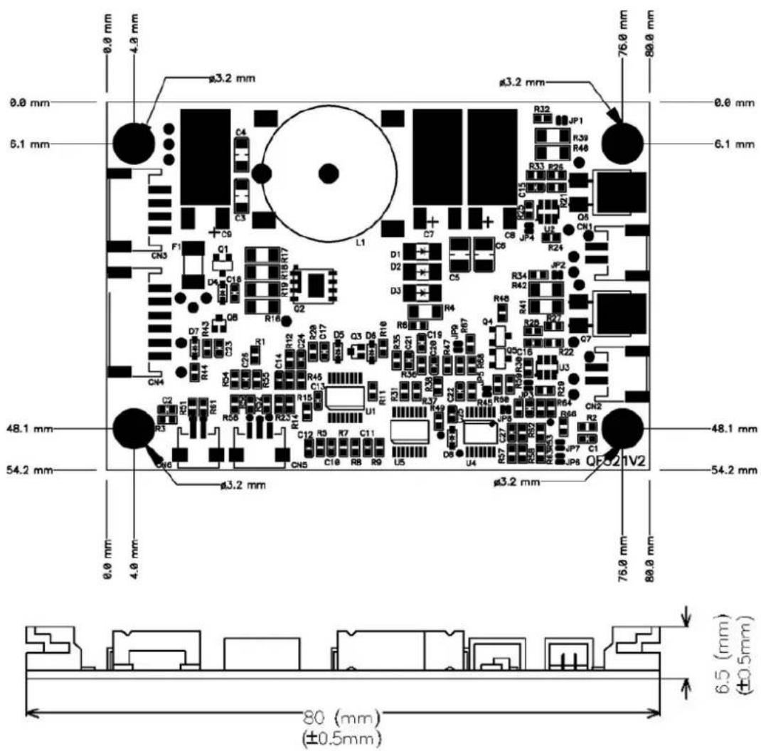
Figure 4.1 Dimensions
Chapter 5
Touchscreen and Controller
5.1 Touchscreen (Optional: for IDK-2119R only)
5.1.1 Touch Characteristics
The touch panel features a resistive-type touchscreen for use with flat LCD displays. When touched, using either a round-ended resin pen or finger, the touch panel circuit identifies the touch coordinates based on the voltage at the point of contact on the screen.
5.1.2 Optical Characteristics
| Item Specifications Remarks | ||||||||
| 1 Transparency 80% ± 3% BYK-Gardner | ||||||||
| 2 | H | a | z | e | 8 | . | 0 | % ± 3% BYK-Gardner |
5.1.3 Environmental Characteristics
| Item Specifications Remarks | |||
| 1 | Operating Temperature | -20 ~ 70 °C | Note: All terms under an atmosphere of 1 |
| 2 | Storage Temperature | -40 ~ 80 °C | |
| 3 | Operating Humidity | 20 ~ 80%RH | |
| 4 | Storage Humidity | 20 ~ 90%RH | |
5.1.4 Mechanical Characteristics
| Item | Specifications | Remarks | ||
| 1 | Surface Hardness | Pencil hardness 3H. | JIS K-5600-5-4150gf, 45° | |
| 2 | FPC Peeling Strength 1) 5N (5N min.)2) 19.6N (19.6N min.) | 1) Peeling upward by 90°2) Peeling downward by 90° | ||
| 3 | Operating Force | Pen | 0.05N ~ 1.96N(5 ~ 200gf) | Dot spacerWithin the guaranteed active area, but not on the age resistor or dot spacer. |
| Finger | ||||
5.1.5 Electronic Characteristics
| Item Specifications | Remarks | |||
| 1 | Rated Voltage | DC 7 V max. | ||
| 2 | Resistance | X axis: 200Ω ~ 500Ω (see figure below) | FPC connector | |
| Y axis: 200Ω ~ 800Ω (see figure below) | ||||
| 3 | Linearity | X ≤1.5% (see figure below) | Reference: 250 gf | |
| Y ≤1.5% (see figure below) | ||||
| 4 | Chattering | ≤ 15ms max. | ||
| 5 | Insulation Resistance | ≥ 20MΩ min. (DC 25 V) | ||
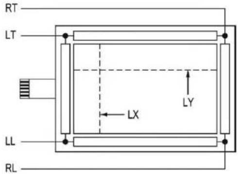
5.1.6 General Specifications
| Item Specifications | ||
| 1 | Frame Size | 393.40 ± 0.50 x 316.65 ± 0.50 mm |
| 2 | Viewing Area | 380.90 ± 0.20 x 305.65 ± 0.20 mm |
| 3 | Active Area | 377.30±0.20 x 302.05 ± 0.20 mm |
| 4 Total Thickness 3.20 ± 0.20 mm | ||
| 5 Tail Length | 305.0 ± 6.0 mm | |
5.2 Touch Controller (Optional: for IDK-2119R only)
The Advantech ETM-RES04C Touch Control Board is the ultimate combo board. This touch panel controller enables the optimum performance of analog-resistive touch panels for 5-wire models. The controller communicates with the PC system directly through USB and RS-232 connector. This design delivers superior sensitivity, accuracy and ease of operation. The touch panel driver emulates the left and right button functions of a mouse and has the following features:
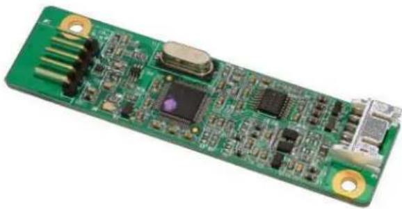
natural_image
Green printed circuit board with various electronic components and gold contacts (no visible text or symbols)5.2.1 Touch Controller Characteristics
5.2.1.1 Specifications
Electrical Features
+5 Vdc/ 100 mA typical, 50 mV peak-to-peak maximum ripple and noise
■ Bi-directional RS-232 serial communication and full speed USB 1.1
■ Maximum report rate is 180 points/sec for RS-232, and 200 points/sec for USB
■ Unaffected by environmental EMI.
The 5-wire model panel resistance is 50 \~ 200 ohm (pin to pin on same layer)
■ Touch resistance under 3K ohm
Serial Interface
■ EIA 232E (Serial RS-232)
■ No parity, 8 data bits, 1 stop bit, 9600 baud (N, 8, 1, 9600)
■ Supports Windows 2000 / Vista / XP/ 7, Windows CE 5.0 / 6.0 / 7.0, Windows NT4, Linux, DOS and QNX
USB Interface
■ Conforms to full-speed USB, Revision 1.1.
If the USB is connected to the controller, the controller will communicate via the USB not the serial port.
■ Supports Windows 2000/ Vista / XP / 7, Windows CE 5.0 / 6.0 / 7.0, Linux and QNX
Touchscreen Resolution
■ Resolution is 2,048 x 2,048
Response Time
Max. 20 ms
5.2.1.2 Environmental Features
Reliability
■ MTBF is 200,000 hours
Temperature Ranges
■ Operating temperature = -25 \~ 85 °C
■ Storage temperature = -25 \~ 85 °C
Relative Humidity
■ Relative humidity is 95% at 60 °C, non-condensing
RoHS certificate complete
Regulatory FCC-B and CE approvals complete
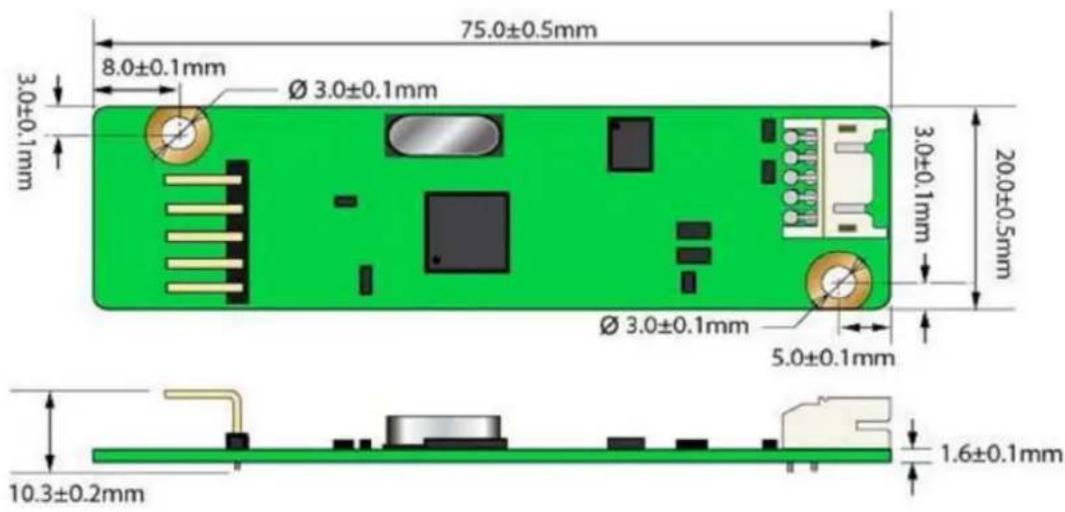
Dimensions: 75 mm x 20 mm x 10 mm
5.2.2 Pin Assignment and Description
5.2.2.1 Connector and LED Locations
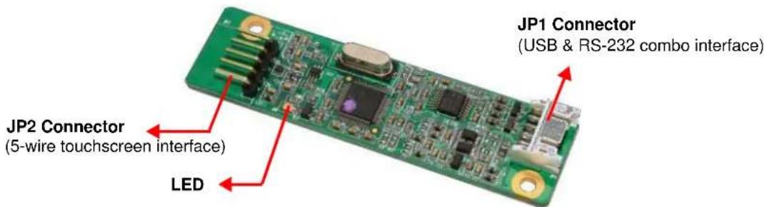
5.2.2.2 JP1 Combo Interface Connector Pins and Signal Descriptions
The combo interface connector, USB and RS-232, is a box, 2.0 mm, 10-pin, 90°, male-type lock connector developed for use with single-wire pins in a 5+5 pin header. The pins are numbered as shown in the following table.
| USB Pin # | Signal Name | Signal Function RS-232 | Pin # | Signal Name | Signal Function |
| 1 G Ground 1 G Ground | |||||
| 2 V USB Power 2 V Power | |||||
| 3 G Ground 3 G Ground | |||||
| 4 D+ USB D+ 4 TxD Serial port | |||||
| 5 D- USB D- | 5 RxD | Serial port | |||
| Signal Name | DB-9 pin # | RS-232 pin # | Sourced By | Signal Description |
| RxD | 2 | 5 | Ctrlr | Serial data from controller to host |
| TxD | 3 | 4 | Host | Serial data from host to controller |
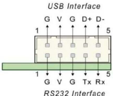
Figure 5.1 Board-mounted header
5.2.2.3 JP2 Touchscreen Connector Pins and Signal Descriptions
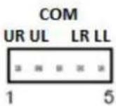
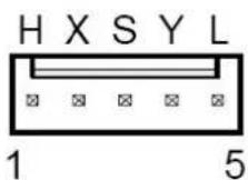
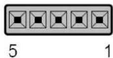
The JP2 touchscreen connector is a single row, 2.54 mm, 5-pin, 90°, male-type connector. The pins are numbered as shown in the following table.
| JP2 Pin # | Signal Name | Signal Description |
| 1 H / UR Drive signal attached to the upper right corner of the touch-screen substrate (from the user's perspective). | ||
| 2 Y / UL | Drive signal attached to the upper left corner of the substrate. | |
| 3 | COM | - |
| 4 | X / LR | Drive signal attached to the lower right corner of the substrate. |
| 5 L / LL | Drive signal attached to the lower left corner of the substrate. | |
5.2.3 Physical Dimensions
ETM-RES04C-EEH4EE Touch Control Board (unit: mm)
Appendix A
Optical Characteristics
A.1 Optical Characteristics
The following optical characteristics are as measured when in stable condition at a room temperature of 25 °C.
Table A.1: Optical Characteristics
| Item | Unit | Conditions | Min. | Typ. | Max. | Note |
| Viewing Angle [degree] | Horizontal (right) 85 - 1 | |||||
| CR = 10 (left) 85 - | ||||||
| Vertical (up) 80 - | ||||||
| CR = 10 (down) | 80 - | |||||
| Luminance Uniformity | [%] | 9 points | 75 | 85 | -2,3 | |
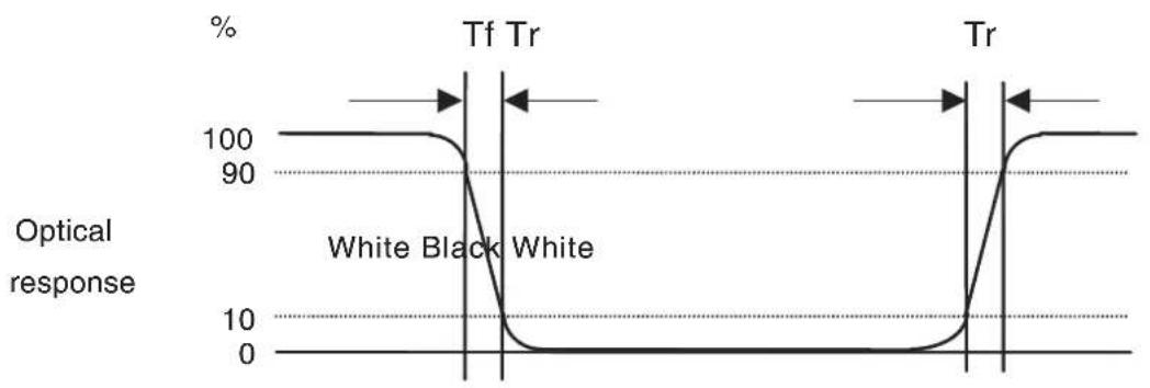
| Optical Response Time | [msec] | Rising | - | 3.6 | 5.7 | |
| Falling | - | 1.4 | 2.35 | |||
| Rising and falling | - | 5 | 8 | |||
| Color / Chromaticity Coordinates (CIE 1931) | White x | - | 0.2582 | -4 | ||
| White y | - | 0.2614 | - | |||
| Color Temp. | K | - | 6500 | - | ||
| White Luminance | [cd/m^2] | 1100 | 1200 - 4 | |||
| Contrast Ratio | - | 1100 | - | |||
Optical equipment: BM-7, DT-101, or equivalent
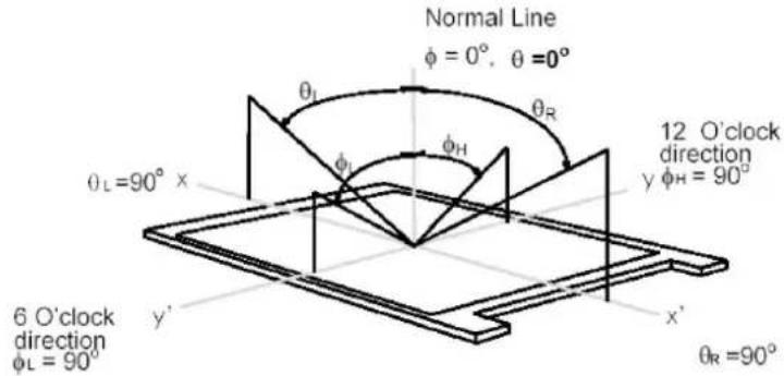
Note 1: The viewing angle is defined as the contrast ratio R10 at the screen center over a 180° horizontal and 180° vertical range (off-normal viewing angles). The 180° viewing angle range is 90° (θ) horizontally left and right, and 90° (Φ) vertically high (up) and low (down). The angle is typically measured from the center of the screen and perpendicular to the display surface when rotating the screen to develop the desired viewing angle.
Note 2: The nine-point position
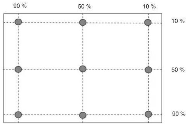
scatter
| Position | Percentage (%) | |---|---| | Top Left | 90 | | Top Right | 50 | | Bottom Left | 10 | | Bottom Right | 50 | | Bottom Center | 90 | | Bottom Right | 50 | | Bottom Center (Right) | 10 |Note 3: The luminance uniformity of the nine points can be determined by dividing the maximum luminance values by the minimum test point luminance
$$ \delta_ {w 9} = \frac {\text { Minimum Brightness of nine points }}{\text { Maximum g Btness of nine points }} $$
Note 4: Regarding the measurement method, the LCD module should be stabilized at a set temperature for 30 minutes to avoid abrupt changes in temperature when measuring. To stabilize the luminance, measurement should be conducted in a dark windowless room after the backlight has been activated for 30 minutes and using DT-100, or an equivalent, as the optical equipment.
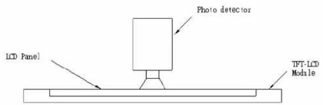
Note 5: Regarding the response time, the photo detector output signals are measured when the input signals are changed from "Full Black" to "Full White" (rising time), and from "Full White" to "Full Black" (falling time). The response time is defined as the interval between the 10% and 90% amplitude points. Please refer to the figure below.
line
| Time Segment | Optical response | | ------------ | ---------------- | | Tf Tr | 100 | | Tr | 100 |Appendix B
Handling Precautions
B.1 Handling Precautions
- Because the front polarizer is vulnerable to damage, we recommend taking additional care not to scratch the polarizer surface.
- Be sure to turn off the power supply when connecting/disconnecting from the input connector.
- In the event of exposure to water or other liquids, immediately wipe off all liquid droplets. Prolonged contact with liquid may cause discoloration or spots.
- To clean the panel surface, wipe with an absorbent cotton or soft cloth.
- Because the panel is made of glass, it is liable to break or crack if dropped or hit with a hard object.
- As CMOS LSI is used in this module, be cautious of static electricity and ensure human earthing when handling.
- Do not open or modify the module assembly.
- Do not bend the reflector sheet at the back of the module in any direction.
- To reinsert the module into the packing container slot, lightly press the far edges of the LED light bar reflector; otherwise the TFT module may be damaged.
- When inserting or removing the signal interface connector, do not rotate or tilt the interface connector on the TFT module.
- After installing the TFT module in an enclosure, do not twist nor bend the TFT module. When designing such enclosures, avoid bending or twisting the TFT module to prevent damage.
- A small amount of material with no flammability grading has been used in the LCD module. The LCD module should be supplied with power that satisfies the requirements of a limited power source (IEC60950 or UL1950); otherwise an exemption must be obtained.
www.advantech.com
Please verify specifications before quoting. This guide is intended for reference purposes only.
All product specifications are subject to change without notice.
No part of this publication may be reproduced in any form or by any means, electronic, photocopying, recording or otherwise, without prior written permission of the publisher.
All brand and product names are trademarks or registered trademarks of their respective companies.
© Advantech Co., Ltd. 2014
- IDK-2119 Series
- Copyright
- Acknowledgements
- Message to the Customer
- Advantech Customer Services
- Technical Support
- Product Warranty (2 years)
- Contents
- Chapter 1 Overview......1
- Chapter 2 Electrical Characteristics......9
- Chapter 3 Signal Characteristics......13
- Chapter 4 Connector and Pin Assignment.....19
- Chapter 5 Touchscreen and Controller...... 23
- Appendix A Optical Characteristics...... 29
- Appendix B Handling Precautions.... 33
- Chapter 1
- General Description
- Specifications
- LCD Panel
- LED Driver Board
- Touchscreen (R series)
- Environment
- Mechanical Characteristics
- IDK-2119N-K2SXA2E
- IDK-2119R-K2SXA2E
- Functional Block Diagram
- Touchscreen Driver
- Absolute Maximum Ratings
- Absolute Ratings for TFT LCD Module
- Absolute Ratings for Backlight Unit
- Absolute Environmental Ratings
- Chapter 2
- Power Specifications
- Backlight Driving Conditions
- Chapter 3
- Pixel Format Image
- Pin Description
- Input Data Format
- Interface Timing
- Timing Characteristics
- Input Timing Diagram
- Power ON/OFF Sequence
- Chapter 4
- Connector and Pin Assignment
- TFT LCD Module
- Connectors
- Pin Assignment
- Backlight Unit
- LED Light Bar Connector Signals
- LED Driver Board
- Specifications
- Input Connector Pin Definition
- Output Connector Pin Definition
- Dimensions
- Chapter 5
- Touchscreen (Optional: for IDK-2119R only)
- Touch Characteristics
- Optical Characteristics
- Environmental Characteristics
- Mechanical Characteristics
- Electronic Characteristics
- General Specifications
- Touch Controller (Optional: for IDK-2119R only)
- Touch Controller Characteristics
- Specifications
- Electrical Features
- Serial Interface
- USB Interface
- Touchscreen Resolution
- Response Time
- Environmental Features
- Reliability
- Temperature Ranges
- Relative Humidity
- RoHS certificate complete
- Pin Assignment and Description
- Connector and LED Locations
- JP1 Combo Interface Connector Pins and Signal Descriptions
- JP2 Touchscreen Connector Pins and Signal Descriptions
- Physical Dimensions
- Appendix A
- A.1 Optical Characteristics
- Appendix B
- B.1 Handling Precautions
- www.advantech.com
Brand : Advantech
Model : IDK-2119N-K2SXA2E
Category : Screen