
MOC3011 - Electronic component Steren - Free user manual and instructions
Find the device manual for free MOC3011 Steren in PDF.


| Product Type | Optocoupler / Optoisolator (Infrared LED + Silicon Bilateral Switch) |
| Model | MOC3011 (IFT = 10 mA max) |
| Package | 6-pin DIP, Style 6 (CASE 730A-04, 730C-04, 730D-05 options) |
| Dimensions (Typical) | 8.13–8.89 mm width, 6.10–6.60 mm height, 2.93–5.08 mm thickness (depending on package variant) |
| Pin Configuration | Pin 1: Anode, Pin 2: Cathode, Pin 3: NC, Pin 4: Main Terminal, Pin 5: Substrate (Do Not Connect), Pin 6: Main Terminal |
| Isolation Voltage | 7500 Vac(pk) for 1 second (60 Hz) |
| LED Forward Current (Continuous, Max) | 60 mA |
| LED Forward Voltage (Typical @ 10 mA) | 1.15 V (max 1.5 V) |
| LED Reverse Voltage (Max) | 3 V |
| Trigger Current (IFT, Max) | 10 mA (to latch output with main terminal voltage = 3 V) |
| Output Off-State Voltage (V_DRM, Max) | 250 V |
| Peak Blocking Current (Max) | 100 nA (at rated V_DRM) |
| Peak On-State Voltage (Max @ 100 mA peak) | 3 V |
| Holding Current (Typical) | 100 µA |
| Critical Rate of Rise of Off-State Voltage (dv/dt, Min) | 10 V/µs (static) |
| Operating Temperature Range | -40 to +85 °C |
| Storage Temperature Range | -40 to +150 °C |
| Junction Temperature Range | -40 to +100 °C |
| Soldering Temperature (10 s) | 260 °C |
| Total Device Power Dissipation @ 25°C | 330 mW (derate 4.4 mW/°C above 25°C) |
| Typical Applications | Solenoid/valve controls, lamp ballasts, motor controls, solid state relays, incandescent lamp dimmers, interfacing microprocessors to 115 Vac peripherals |
| Certification Option | Suffix "V" for devices tested and marked per VDE 0884 |
Frequently Asked Questions - MOC3011 Steren
User questions about MOC3011 Steren
0 question about this device. Answer the ones you know or ask your own.
Ask a new question about this device
Download the instructions for your Electronic component in PDF format for free! Find your manual MOC3011 - Steren and take your electronic device back in hand. On this page are published all the documents necessary for the use of your device. MOC3011 by Steren.
USER MANUAL MOC3011 Steren
The MOC3010 Series consists of gallium arsenide infrared emitting diodes, optically coupled to silicon bilateral switch and are designed for applications requiring isolated triac triggering, low-current isolated ac switching, high electrical isolation (to 7500 Vac peak), high detector standoff voltage, small size, and low cost.
- To order devices that are tested and marked per VDE 0884 requirements, the suffix "V" must be included at end of part number. VDE 0884 is a test option.
Recommended for 115 Vac(rms) Applications:
- Solenoid/Valve Controls
- Lamp Ballasts
• Interfacing Microprocessors to 115 Vac Peripherals
- Motor Controls
• Static ac Power Switch
- Solid State Relays
• Incandescent Lamp Dimmers
MAXIMUM RATINGS ( T_A = 25^ unless otherwise noted)
| Rating Symbol Value Unit |
INFRARED EMITTING DIODE
| Reverse Voltage V | R | 3 Volts | |
| Forward Current — Continuous I | F | 60 mA | |
| Total Power Dissipation @ TA = 25°C Negligible Power in Transistor Derate above 25°C | PD | 100 | mW |
| 1.33 | mW/°C |
OUTPUT DRIVER
| Off-State Output Terminal Voltage V | DRM | 250 | Volts |
| Peak Repetitive Surge Current(PW = 1 ms, 120 pps) | I_TSM | 1 | A |
| Total Power Dissipation @ T_A = 25°CDerate above 25°C | P_D | 3004 | mWmW/°C |
TOTAL DEVICE
| Isolation Surge Voltage(1)(Peak ac Voltage, 60 Hz, 1 Second Duration) | V_ISO | 7500 | Vac(pk) |
| Total Power Dissipation @ T_A = 25°C Derate above 25°C | P_D | 3304.4 | mWmW/°C |
| Junction Temperature Range | T_J | -40 to +100 | °C |
| Ambient Operating Temperature Range(2) | T_A | -40 to +85 | °C |
| Storage Temperature Range(2) | T_stg | -40 to +150 | °C |
| Soldering Temperature (10 s) | T_L | 260 | °C |
- Isolation surge voltage, V_ISO , is an internal device dielectric breakdown rating. For this test, Pins 1 and 2 are common, and Pins 4, 5 and 6 are common.
- Refer to Quality and Reliability Section in Opto Data Book for information on test conditions. Preferred devices are Motorola recommended choices for future use and best overall value. GlobalOptoisolator is a trademark of Motorola, Inc.
(Replaces MOC3009/D)
MOC3010
[IFT = 15 mA Max]
MOC3011
[IFT = 10 mA Max]
MOC3012\*
[IFT = 5 mA Max]
*Motorola Preferred Device
STYLE 6 PLASTIC

STANDARD THRU HOLE
CASE 730A-04
COUPLER SCHEMATIC

- ANODE
- CATHODE
- NC
- MAIN TERMINAL
- SUBSTRATE DO NOT CONNECT
- MAIN TERMINAL
MOC3010 MOC3011 MOC3012
ELECTRICAL CHARACTERISTICS ( T_A = 25^ unless otherwise noted)
| Characteristic Symbol Min Typ Max Unit |
INPUT LED
| Reverse Leakage Current (V_R = 3 V) | I_R | — 0.05 | 100 × A | ||
| Forward Voltage (I_F = 10 mA) | V_F | — 1.15 | 1.5 Volts |
OUTPUT DETECTOR (IF = 0 unless otherwise noted)
| Peak Blocking Current, Either Direction (Rated V_DRM^(1) ) | I_DRM | — 10 100 nA | ||
| Peak On-State Voltage, Either Direction (ITM = 100 mA Peak) | V_TM | — 1.8 3 Volts | ||
| Critical Rate of Rise of Off-State Voltage (Figure 7, Note 2) | dv/dt | — 10 | — | V/ × s |
COUPLED
| LED Trigger Current, Current Required to Latch Output(Main Terminal Voltage = 3 V(3)) | IFT | mA | ||||
| — | 8 | 15 | ||||
| — | 5 | 10 | ||||
| — | 3 | 5 | ||||
| Holding Current, Either Direction | IH | — 100 | —∞A | |||
- Test voltage must be applied within dv/dt rating.
- This is static dv/dt. See Figure 7 for test circuit. Commutating dv/dt is a function of the load–driving thyristor(s) only.
- All devices are guaranteed to trigger at an I_F value less than or equal to max I_FT . Therefore, recommended operating I_F lies between max I_FT (15 mA for MOC3010, 10 mA for MOC3011, 5 mA for MOC3012) and absolute max I_F (60 mA).
TYPICAL ELECTRICAL CHARACTERISTICS
$$ \mathsf {T A} = 2 5 ^ {\circ} \mathsf {C} $$

line
| IF, LED FORWARD CURRENT (mA) | VF, FORWARD VOLTAGE (VOLTS) - PULSE ONLY | VF, FORWARD VOLTAGE (VOLTS) - PULSE OR DC | | --------------------------- | ---------------------------------------- | ----------------------------------------- | | 1 | 1.0 | 1.1 | | 10 | 1.2 | 1.3 | | 100 | 1.6 | 1.7 | | 1000 | 2.0 | 2.0 |Figure 1. LED Forward Voltage versus Forward Current

line
| V_TM, ON-STATE VOLTAGE (VOLTS) | I_TM, ON-STATE CURRENT (mA) | | ------------------------------ | -------------------------- | | -3 | -800 | | -2 | -400 | | -1 | 0 | | 0 | 0 | | 1 | 0 | | 2 | 0 | | 3 | 0 | | 4 | +400 | | 5 | +800 |Figure 2. On-State Characteristics
line
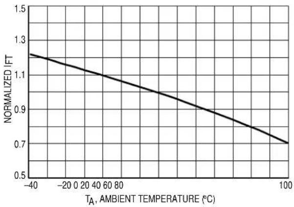
| TA, AMBIENT TEMPERATURE (°C) | NORMALIZED IFT | | --------------------------- | -------------- | | -40 | 1.25 | | 100 | 0.7 |Figure 3. Trigger Current versus Temperature

line
| PWin, LED TRIGGER WIDTH (∞s) | IFT, NORMALIZED LED TRIGGER CURRENT | | ----------------------------- | ------------------------------------- | | 1 | 25 | | 2.5 | 10 | | 50 | 5 | | 100 | 1 |Figure 4. LED Current Required to Trigger versus LED Pulse Width

line
| TA Ambient Temperature (°C) | dv/dt. STATIC (V/×s) | | --------------------------- | -------------------- | | 25 | 10 | | 30 | 9 | | 50 | 8 | | 70 | 7 | | 100 | 6 | | 1000 | 5 | | 10000 | 4 | | 100000 | 3 | | 1000000 | 2 | | 10000000 | 1 |Figure 5. dv/dt versus Temperature

line
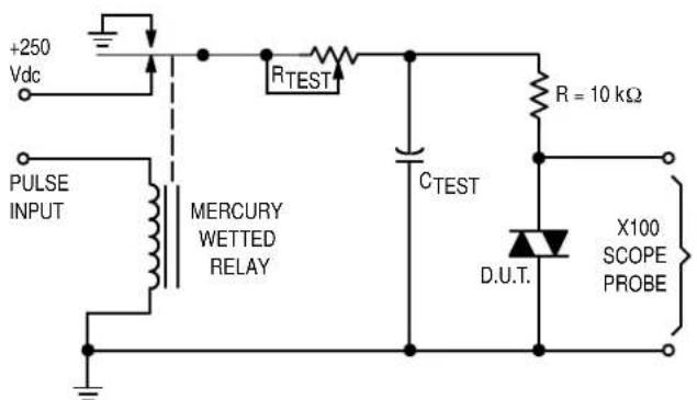
| Parameter | Value | | ----------------- | --------- | | Vmax | 250 V | | dv/dt | 0.63 Vmax / τRC | | Current (τ_RC) | 0 |- The mercury wetted relay provides a high speed repeated pulse to the D.U.T.
- 100x scope probes are used, to allow high speeds and voltages.
- The worst-case condition for static dv/dt is established by triggering the D.U.T. with a normal LED input current, then removing the current. The variable RTEST allows the dv/dt to be gradually increased until the D.U.T. continues to trigger in response to the applied voltage pulse, even after the LED current has been removed. The dv/dt is then decreased until the D.U.T. stops triggering. rRC is measured at this point and recorded.
Figure 6. Static dv/dt Test Circuit
MOC3010 MOC3011 MOC3012
TYPICAL APPLICATION CIRCUITS
NOTE: This optoisolator should not be used to drive a load directly. It is intended to be a trigger device only. Additional information on the use of the MOC3010/3011/3012 is available in Application Note AN-780A.

Figure 7. Resistive Load

Figure 8. Inductive Load with Sensitive Gate Triac ( I_GT ≤ 15 mA )

Figure 9. Inductive Load with Non-Sensitive Gate Triac (15 mA < IGT < 50 mA)
PACKAGE DIMENSIONS

NOTES:
1. DIMENSIONING AND TOLERANCING PER ANSI Y14.5M, 1982.
2. CONTROLLING DIMENSION: INCH.
3. DIMENSION L TO CENTER OF LEAD WHEN FORMED PARALLEL.
| DIM | MILLIMETERSINCHES | |||
| MIN MAX | MIN MAX | |||
| A 0 | 320 0.350 | 8.13 8.89 | ||
| B 0 | 240 0.260 | 6.10 6.60 | ||
| C 0 | 115 0.200 | 2.93 5.08 | ||
| D 0 | 016 0.020 | 0.41 0.50 | ||
| E 0 | 040 0.070 | 1.02 1.77 | ||
| F 0 | 010 0.014 | 0.25 0.36 | ||
| G | 0.100 BSC | 2.54 BSC | ||
| J 0 | 008 0.012 | 0.21 0.30 | ||
| K 0 | 100 0.150 | 2.54 3.81 | ||
| L | 0.300 BSC | 7.62 BSC | ||
| M | 0° | 15° | 0° | 15° |
| N 0 | 015 0.100 | 0.38 2.54 | ||
STYLE 6:
PIN 1. ANODE
2. CATHODE
3. NC
4. MAIN TERMINAL
5. SUBSTRATE
6. MAIN TERMINAL
CASE 730A-04
ISSUE G

CASE 730C-04
ISSUE D
NOTES:
1. DIMENSIONING AND TOLERANCING PER ANSI Y14.5M, 1982.
2. CONTROLLING DIMENSION: INCH.
| MILLIMETERSINCHES | ||||
| DIM | MIN MAX | MIN MAX | ||
| A 0 | 320 0.350 | 8.13 8.89 | ||
| B 0 | 240 0.260 | 6.10 6.60 | ||
| C 0 | 115 0.200 | 2.93 5.08 | ||
| D 0 | 016 0.020 | 0.41 0.50 | ||
| E 0 | 040 0.070 | 1.02 1.77 | ||
| F 0 | 010 0.014 | 0.25 0.36 | ||
| G | 0.100 BSC 2.54 BSC | |||
| H 0 | 020 0.025 | 0.51 0.63 | ||
| J 0 | 008 0.012 | 0.20 0.30 | ||
| K 0 | 006 0.035 | 0.15 0.88 | ||
| L | 0.320 BSC | 8.13 BSC | ||
| S 0 | 332 0.390 | 8.43 9.90 | ||
*Consult factory for leadform option availability
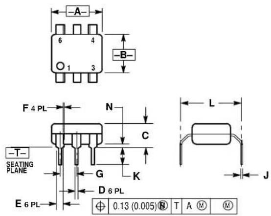
CASE 730D-05
ISSUE D
NOTES:
1. DIMENSIONING AND TOLERANCING PER ANSI
Y14.5M.1982
2. CONTROLLING DIMENSION: INCH.
3. DIMENSION L TO CENTER OF LEAD WHEN
FORMED PARALLEL.
| DIM | MILLIMETERSINCHES | |||
| MIN MAX | MIN MAX | |||
| A 0 | 320 0.350 | 8.13 8.89 | ||
| B 0 | 240 0.260 | 6.10 6.60 | ||
| C 0 | 115 0.200 | 2.93 5.08 | ||
| D 0 | 016 0.020 | 0.41 0.50 | ||
| E 0 | 040 0.070 | 1.02 1.77 | ||
| F 0 | 010 0.014 | 0.25 0.36 | ||
| G 0 | 100 BSC | 2.54 BSC | ||
| J 0 | 008 0.012 | 0.21 0.30 | ||
| K 0 | 100 0.150 | 2.54 3.81 | ||
| L 0 | 400 0.425 | 10.16 | 10.80 | |
| N 0 | 015 0.040 | 0.38 1.02 | ||
*Consult factory for leadform option availability
Motorola reserves the right to make changes without further notice to any products herein. Motorola makes no warranty, representation or guarantee regarding the suitability of its products for any particular purpose, nor does Motorola assume any liability arising out of the application or use of any product or circuit, and specifically disclaims any and all liability, including without limitation consequential or incidental damages. "Typical" parameters can and do vary in different applications. All operating parameters, including "Typicals" must be validated for each customer application by customer's technical experts. Motorola does not convey any license under its patent rights nor the rights of others. Motorola products are not designed, intended, or authorized for use as components in systems intended for surgical implant into the body, or other applications intended to support or sustain life, or for any other application in which the failure of the Motorola product could create a situation where personal injury or death may occur. Should Buyer purchase or use Motorola products for any such unintended or unauthorized application, Buyer shall indemnify and hold Motorola and its officers, employees, subsidiaries, affiliates, and distributors harmless against all claims, costs, damages, and expenses, and reasonable attorney fees arising out of, directly or indirectly, any claim of personal injury or death associated with such unintended or unauthorized use, even if such claim alleges that Motorola was negligent regarding the design or manufacture of the part. Motorola and (A) are registered trademarks of Motorola, Inc. Motorola, Inc. is an Equal Opportunity/Affirmative Action Employer.
How to reach us:
USA/EUROPE: Motorola Literature Distribution;
P.O. Box 20912; Phoenix, Arizona 85036. 1-800-441-2447
MFAX: RMFAX0@email.sps.mot.com - TOUCHTONE (602) 244-6609
INTERNET: http://Design-NET.com
JAPAN: Nippon Motorola Ltd.; Tatsumi-SPD-JLDC. Toshikatsu Otsuki.
6F Seibu-Butsuryu-Center, 3-14-2 Tatsumi Koto-Ku, Tokyo 135, Japan. 03-3521-8315
HONG KONG: Motorola Semiconductors H.K. Ltd.; 8B Tai Ping Industrial Park,
51 Ting Kok Road, Tai Po, N.T., Hong Kong. 852-26629298


Brand : Steren
Model : MOC3011
Category : Electronic component