
ECU-1170 - Industrial electronics Advantech - Free user manual and instructions
Find the device manual for free ECU-1170 Advantech in PDF.

| Product Type | Industrial electronics (industrial computer / Edge gateway) |
| Brand | Advantech |
| Model | ECU-1170 |
| Power Supply | 10 to 30 VDC, 2.7 to 0.9 A (UL certified or SELV source) |
| Storage Temperature | -30 °C to 70 °C |
| Operating Environment | Indoor, non-polluted, restricted access location |
| Main Functions | Industrial control, data acquisition, Edge connectivity (Edgelink) |
| Maintenance and Cleaning | Disconnect before cleaning; use a damp cloth without detergent |
| Safety | Mandatory grounding; do not open; do not cover openings; do not expose to moisture or liquids |
| Spare Parts and Repairability | No user-serviceable parts; return to manufacturer for repair |
| Battery | Replace only with the same type or recommended equivalent; follow disposal instructions |
| Installation | Open-type equipment to be installed in a suitable enclosure |
| Compliance | Designed for use with a UL certified power source |
Frequently Asked Questions - ECU-1170 Advantech
User questions about ECU-1170 Advantech
0 question about this device. Answer the ones you know or ask your own.
Ask a new question about this device
Download the instructions for your Industrial electronics in PDF format for free! Find your manual ECU-1170 - Advantech and take your electronic device back in hand. On this page are published all the documents necessary for the use of your device. ECU-1170 by Advantech.
USER MANUAL ECU-1170 Advantech
natural_image
Illustration of three stacked electronic devices with no visible text or symbolsECU-1170
High-Performance All-in-One Gateway for Battery Energy Storage Systems
Copyright
The documentation and the software included with this product are copyrighted 2025 by Advantech Co., Ltd. All rights are reserved. Advantech Co., Ltd. reserves the right to make improvements in the products described in this manual at any time without notice. No part of this manual may be reproduced, copied, translated, or transmitted in any form or by any means without the prior written permission of Advantech Co., Ltd. The information provided in this manual is intended to be accurate and reliable. However, Advantech Co., Ltd. assumes no responsibility for its use, nor for any infringements of the rights of third parties that may result from its use.
Acknowledgments
Intel, Pentium, Celeron and Atom are trademarks of Intel Corporation.
Microsoft Windows and MS-DOS are registered trademarks of Microsoft Corp.
All other product names or trademarks are properties of their respective owners.
Support
For more information on this and other Advantech products, please visit our websites at: http://www.advantech.com
For technical support and service, please visit our support website at: http://www.advantech.com/support/
Part No. 2003U11700 Edition 1
Printed in China March 2025
Declaration of Conformity
CE
This product has passed the CE test for environmental specifications when shielded cables are used for external wiring. We recommend the use of shielded cables. This type of cable is available from Advantech. Please contact your local supplier for ordering information.
Test conditions for passing also include the equipment being operated within an industrial enclosure. In order to protect the product from damage caused by electrostatic discharge (ESD) and EMI leakage, we strongly recommend the use of CE-compliant industrial enclosure products.
FCC Class A
This equipment has been tested and found to comply with the limits for a Class A digital device, pursuant to part 15 of the FCC Rules. These limits are designed to provide reasonable protection against harmful interference when the equipment is operated in a commercial environment. This equipment generates, uses, and can radiate radio frequency energy and, if not installed and used in accordance with the instruction manual, may cause harmful interference to radio communications. Operation of this equipment in a residential area is likely to cause harmful interference. In this event, users are required to correct the interference at their own expense.
Technical Support and Assistance
- Visit the Advantech website at www.advantech.com/support to obtain the latest product information.
- Contact your distributor, sales representative, or Advantech's customer service center for technical support if you need additional assistance. Please have the following information ready before calling:
– Product name and serial number
– Description of your peripheral attachments
– Description of your software (operating system, version, application software, etc.)
– A complete description of the problem
– The exact wording of any error messages
Safety Precaution - Static Electricity
Follow these simple precautions to protect yourself from harm and the products from damage.
To avoid electrical shock, always disconnect the power from the PC chassis before manual handling. Do not touch any components on the CPU card or other cards while the PC is powered on.
- Disconnect the power before making any configuration changes. A sudden rush of power after connecting a jumper or installing a card may damage sensitive electronic components.
Safety Instructions
- Read these safety instructions carefully.
- Retain this user manual for future reference.
- Disconnect the equipment from all power outlets before cleaning. Use only a damp cloth for cleaning. Do not use liquid or spray detergents.
-
For pluggable equipment, the power outlet socket must be located near the equipment and easily accessible.
-
Protect the equipment from humidity.
-
Place the equipment on a reliable surface during installation. Dropping or letting the equipment fall may cause damage.
-
The openings on the enclosure are for air convection. Protect the equipment from overheating. Do not cover the openings.
-
Ensure that the voltage of the power source is correct before connecting the equipment to a power outlet.
-
Position the power cord away from high-traffic areas. Do not place anything over the power cord.
-
All cautions and warnings on the equipment should be noted.
-
If the equipment is not used for a long time, disconnect it from the power source to avoid damage from transient overvoltage.
-
Never pour liquid into an opening. This may cause fire or electrical shock.
-
Never open the equipment. For safety reasons, the equipment should be opened only by qualified service personnel.
-
If any of the following occurs, have the equipment checked by service personnel:
-
The power cord or plug is damaged.
– Liquid has penetrated the equipment.
– The equipment has been exposed to moisture. -
The equipment is malfunctioning, or does not operate according to the user manual.
– The equipment has been dropped and damaged.
– The equipment shows obvious signs of breakage. -
DO NOT LEAVE THIS EQUIPMENT IN AN ENVIRONMENT WHERE THE STORAGE TEMPERATURE MAY GO BELOW -30°C (-22°F) OR ABOVE 70°C (158°F). THIS COULD DAMAGE THE EQUIPMENT. THE EQUIPMENT SHOULD BE IN A CONTROLLED ENVIRONMENT.
-
CAUTION: DANGER OF EXPLOSION IF BATTERY IS INCORRECTLY REPLACED. REPLACE ONLY WITH THE SAME OR EQUIVALENT TYPE RECOMMENDED BY THE MANUFACTURER, DISCARD USED BATTERIES ACCORDING TO THE MANUFACTURER'S INSTRUCTIONS.
-
This product is intended to be supplied by an UL certified power supply or dc source with SELV output, rated 10 to 30Vdc, 2.7 to 0.9A minimum and maximum ambient temperature (Tma) 70 degree C minimum without power source or adapter. If you need further assistance, please contact Advantech for further information.
-
Ensure that the voltage of the power source is correct before connecting the equipment to a power outlet. The power outlet socket should have a grounded connection.
-
For use in pollution free environments and indoor use.
-
This equipment is not suitable for use in locations where children are likely to be present.
-
If the equipment is used in a manner not specified by the Advantech, the protection provided by the equipment may be impaired.
- The equipment contains no user-serviceable parts. Do not open, Return to manufacturer for servicing.
- Do not block air ventilation holes.
- This is open type equipment and should be installed in a suitable enclosure.
- Equipment is intended for installation in Restricted Access Area.
Chapter 2 Hardware Functionality......7
2.1 Overview ...... 8
Figure 2.1 ECU-1170 Overview...... 8
2.2 LED Status Indicators and Buttons 9
2.2.1 System Status Indicators .... 9
Figure 2.2 System Status LED .... 9
Table 2.1: System Status Indicators.... 9
2.2.2 Ethernet Status Indicators....9
Figure 2.3 Ethernet Status Indicators ....9
Table 2.2: Ethernet Status Indicators ....9
2.3 System Button.... 10
Figure 2.4 System Button 10
Table 2.3: System Button 10
Table 2.4: Table 2.4: Recovery Options.... 10
Chapter 3 Pins, Jumper Settings, and Wiring ..11
3.1 Power Supply.... 12
Figure 3.1 Power Supply .... 12
Table 3.1: Power Supply .... 12
3.2 Ethernet Ports .... 12
Figure 3.2 Ethernet Ports.... 12
Table 3.2: Ethernet Ports.... 12
3.3 USB Ports .... 13
3.3.1 1 x USB2.0 HOST, 1 x USB3.0 HOST.... 13
Figure 3.3 USB Ports.... 13
Table 3.3: USB Ports.... 13
3.3.2 1 x USB3.0 OTG (Function Reserved) .... 14
Table 3.4: OTG Jumper Settings.... 14
Figure 3.4 USB3.0 OTG .... 14
3.4 Console Ports....15
Figure 3.5 Console Ports....15
Table 3.5: Console Ports....15
3.5 HDMI Ports 16
Figure 3.6 HDMI Ports.... 16
Table 3.6: HDMI Ports.... 16
3.6 CAN Ports.... 17
Figure 3.7 CAN Ports-1 17
Table 3.7: CAN Ports 17
Figure 3.8 CAN Ports-2 17
3.7 Analog Input Ports 18
Figure 3.9 Analog Input Ports.... 18
Table 3.8: Analog Input Ports.... 18
Table 3.9: Voltage/Current Jumper Settings 18
Figure 3.10Voltage/Current Jumper Settings 18
3.8 Serial Ports 19
Figure 3.11 Serial Ports 19
Table 3.10: Serial Ports.... 19
Table 3.11:RS-232/485 Jumper Settings 19
Figure 3.12RS-232/485 Jumper Settings 19
Table 3.12:RS-232/485 Termination Resistors 20
Figure 3.13RS-232/485 Termination Resistors 20
3.9 Digital Inputs 0\~3 (Wet Contacts) 21
Figure 3.14Digital Input 0\~3 (Wet Contacts) -1 ...... 21
Table 3.13:Digital Input 0\~3 (Wet Contacts) 21
Figure 3.15Digital Input 0\~3 (Wet Contacts) -2 ...... 21
3.10 Digital Inputs 4\~19 (Dry/Wet Contacts).... 22
Figure 3.16Digital Inputs 4\~19 (Dry/Wet Contacts) -1....22
Table 3.14: Digital Inputs 4\~19 (Dry/Wet Contacts).... 22
Figure 3.17Digital Input 4\~19 (Dry/Wet Contacts) -2....22
3.11 Digital Output 0\~1 (Low Side Drive)....23
Figure 3.18Digital Output 0\~1 (Low Side Drive) -1....23
Table 3.15: Digital Output 0\~1 (Low Side Drive).... 23
Figure 3.19Digital Output 0\~1 (Low Side Drive) -2....23
3.12 Digital Output 0\~3 (High Side Drive).... 24
Figure 3.20Digital Output 0\~3 (High Side Drive) 24
Table 3.16:Digital Output 0\~3 (High Side Drive) 24
Figure 3.21 Digital Output 0\~3 (High Side Drive) 24
3.13 Digital Output 0\~7 (Relay Output).... 25
Figure 3.22Digital Output 0\~7 (Relay Output) - 1.... 25
Table 3.17:Digital Output 0\~7 (Relay Output) 25
Figure 3.23Digital Output 0\~7 (Relay Output) - 2.... 25
3.14 SD And SIM Slots 26
Figure 3.24SD and SIM slots.... 26
Table 3.18: Location of Mini-PCIe and M.2 Socket 26
Figure 3.25 Location of Mini-PCIe and M.2 Socket 26
Chapter 4 Installation
27
4.1 Jumper and RTC Battery Location.... 28
4.2 DIN Rail And Wall Mount Installation 29
4.3 Module Installation 30
4.3.1 M.2 Slot Module Assembly 30
Table 4.1: M.2 Slot Module Assembly.... 30
Figure 4.1 M.2 Slot Module Assembly.... 30
4.3.2 5G Module Assembly.... 31
Table 4.2: 5G Module Assembly 31
Figure 4.2 5G Module Assembly 32
4.3.3 Mini-PCIe Slot Module Assembly 33
Table 4.3: Mini-PCIe Slot Module Assembly.... 33
Figure 4.3 Mini-PCIe Slot Module Assembly.... 33
Chapter 1
Overview
1.1 Introduction
The ECU-1170 is a purpose-built gateway designed specifically for Battery Energy Storage System (BESS) applications. Featuring integrated multi-I/O interfaces and paired with EdgeLink software, the ECU-1170 supports a wide range of communication protocols, enabling seamless connectivity between various BESS sub-systems. With its high computational performance, the ECU-1170 not only functions as a robust gateway, but also serves as a local EMS (Energy Management System) or a BAU (Battery Auxiliary Unit), offering exceptional versatility and efficiency for energy storage solutions.

natural_image
Exterior view of a black ECU-1179 network device with green connectors and ports (no visible text or symbols on main body)1.2 Specifications
1.2.1 General
| Table 1.1: General | |
| Certifications CE, FCC, UL 62368, IEC-62368 | |
| Dimensions 183 x 108 x 43 mm | |
| Power Input 10 ~ 30 VDC | |
| Mounting Din Rail/Wall-Mount | |
| Ingress Protection | IP30 |
| Storage Temperature | -40 ~ 85°C |
| Operating Temperature | -40 ~ 70°C |
| Humidity | 5-95% (non-condensing) |
| Operating System | Primary: Yocto Linux with EdgelinkSecondary: Ubuntu 22.04 (Linux kernel 5.10) |
1.2.2 System
Table 1.2: System
| CPU | Rockchip RK3568J Quad-Core Arm Cortex A55 1.4GHz (Up to 1.8GHz) |
| RAM 4GB LPDDR4 (Up to 8GB) | |
| eMMC 32GB eMMC (up to 128GB) | |
| Extension Storage 1 x NVMe (Optional by customization) | |
| Display 1 x HDMI (Up to 1080p @120Hz and 4096 x 2304 @60Hz) | |
| Real Time Clock Yes | |
| Watchdog Timer Yes | |
| TPM2.0 Optional by customization | |
| Super-Capacitor Optional by customization (5 seconds power hold upon power loss) | |
| LED 6 x LED (1 x power, 5 x programmable LED) | |
1.2.3 I/O Interfaces
Table 1.3: I/O Interfaces
| Serial | 8 x isolated RS-485/232, 2000VDC isolation | ||
| COM1 COM2 COM3 COM4 COM5 COM6 COM7 COM8 | |||
| Mode | RS-232/485 | ||
| Speed | 50 ~ 115200 bps | 1200 ~ 115200 bps | |
| Data bit | 5,6,7,8 | 8 | |
| Isolation 2000 VDC | |||
| LAN | 4 x 10/100/1000Mbps Ethernet | ||
| USB | 1 x USB2.0 HOST, 1 x USB3.0 HOST (OTG function reserved) | ||
| CAN | 2 x Isolated CAN2.0B, 2000VDC isolation (20Kbps~1000Kbps) | ||
| SD Card | 1 x Micro SD Card Slot | ||
| Expansion Slot | 1 x Mini-PCIe (full-size) Signal: PCIe for WI-FI (optional USB2.0/SATA by customization)1 x M.2 B-Key (2280) Signal: USB2.0,USB3.0 for LTE or 5G (Optional PCIe for NVMe by customization) | ||
| SIM Card | 2 x Nano SIM card slot for redundancy | ||
| ADC | 2 x AI0-20mA or 0-10V (jumper optional), Accuracy 1%, sampling rate: 40sps | ||
| DI | 4 x isolated DI (wet contact)16 x isolated DI (dry & wet contact)2000VDC isolation | ||
| DO(LSD, HSD) | 4 x Isolated HSD, Source Type, 10-30V, 1A 2 x isolated LSD, Sink Type, 10-30V, 1A 2000VDC isolation | ||
| DO(Relay Output) | 8 x Isolated relay (Form A): 5A@250VAC; 3A@30VDCBreakdown voltage: 750VACInitial insulation 1GΩ at 500VDC | ||
| Console | 1 x RS-232 (RJ-45) | ||
1.2.4 Edgelink\*
| Table 1.4: Edgelink Table 1.5: | |
| NorthBound Protocol | IEC-61850*, Modbus Server, DNP3 Outstation, BACnet Server, OPC UA Server |
| SouthBound Protocol | Modbus Client, DNP3Master, DL/T645, IEC-101, IEC-103, IEC-104, OPC UA Client, BACnetIP, BACnet MS/TP, SNMP |
| PLC Driver | ABB/Advantech/Allen-Bradley/BECKHOFF/ DELTA/FATEK/GE/Honeywell/Keyence/Mitsubishi/Omron/Panasonic/Schneider/Sharp/Siemens/ Toyopuc/Wago 750/Yaskawa/Yokogawa |
| Configuration Tool WISE-EdgeLink Studio | |
| Data Monitoring 20000 Tags Max | |
| Cloud Connectivity (MQTT) | Azure, AWS, Google Cloud IoT Core, and more |
| Database Transmission SQL Server, MySQL, ORACLE, FTP Server | |
| VPN OpenVPN | |
*Please refer to EdgeLink specifications for further details. Activation of the IEC-61850 protocol requires an additional fee.
1.3 Software Configurations
| Table 1.6: Software Configurations | |
| Operating System: | Ubuntu 22.04 / Yocto+EdgeLink |
| Programming: | IEC-61131-3, Linux C, Python |
| Login Details: User Name: root | |
| Password: no password (press "Enter") | |
| Default IP: | LAN1: 10.0.0.1 |
| LAN2: 11.0.0.1 | |
| LAN3: 12.0.0.1 | |
| LAN4: 13.0.0.1 | |
1.4 Chassis Dimensions
Figure 1.1 ECU-1170 Chassis Dimensions
1.5 Packing List
The accessory package of the ECU-1170 contains the following items:
(A) ECU-1170
(B) Connectors
(C) Din Rail
(D) Screws
Chapter 2
Hardware
Functionality
2.1 Overview
natural_image
Line drawing of a multi-chamber network device labeled 'ACU-1170' with ports and connectors (no text beyond label)
Figure 2.1 ECU-1170 Overview
2.2 LED Status Indicators and Buttons
2.2.1 System Status Indicators

Figure 2.2 System Status LED
Table 2.1: System Status Indicators
| LED Description |
| PWR Power On |
| PLx Programmable LED |
2.2.2 Ethernet Status Indicators
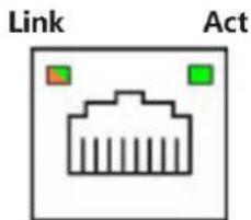
Figure 2.3 Ethernet Status Indicators
Table 2.2: Ethernet Status Indicators
| LED Status Description | |
| Link | Off 10 Mbps |
| Orange 100 Mbps | |
| Green 1000 Mbps | |
| Act | Green Lighting Not transmitting data |
| Green Blinking Transmitting data | |
2.3 System Button

Figure 2.4 System Button
Table 2.3: System Button
| Button Description |
| RCY Recovery |
| RST Reset |
Caution! The RCY button is used for recovering the system. This will erase your project and restore the system.

- Ensure the device is turned off.
- Press and hold the RCY button while turning the device on.
- After powering on, continue holding the RCY button for 10 seconds and observe the upgrade indicator (PL1). Once it starts flashing in a regular pattern, release the RCY button. The device will then begin the recovery process.
- Wait for 3 minutes until the upgrade indicator (PL1) stops flashing, indicating that the recovery is complete.
Note! Recovery restores the last updated image, not the factory image.

Table 2.4: Table 2.4: Recovery Options
| OS Yocto + EdgeLink Ubuntu | ||
| Image that Supports Recovery | Supported from 2.8.4.2 and above | Supported from 1.0.3 and above |
| Folders/Files that Will Be Retained | #/home/sysuser/project/elic (license file) #/home/sysuser/project/edgelink.lic (license file) | None |
Chapter 3
Pins, Jumper Settings, and Wiring
3.1 Power Supply
The ECU-1170 supports a power input range of 10\~30 VDC
DC-In Connector Wiring
- Must be installed by a skilled professional.
- Only use copper conductors.
- Choose the appropriate wire diameter.
- The terminal block is suitable for a 14 AWG torque value of 7 in-lbf.
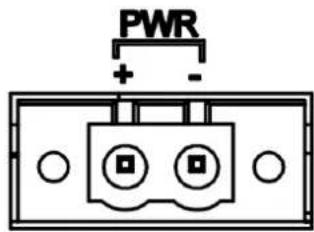
Figure 3.1 Power Supply
Table 3.1: Power Supply
| Pin Charge Description |
| + DC power in V+ |
| - DC power in V- |
3.2 Ethernet Ports
4 x 10/100/1000 Mpbs Ethernet ports
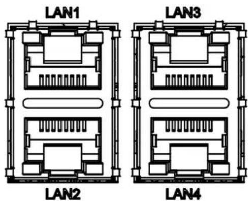
Figure 3.2 Ethernet Ports
Table 3.2: Ethernet Ports
| Pin Number Description |
| A1/B1 MDI0+ |
| A2/B2 MDI0- |
| A3/B3 MDI1+ |
| A4/B4 MDI1- |
| A5/B5 MDI2+ |
| A6/B6 MDI2- |
| A7/B7 MDI3+ |
| A8/B8 MDI3- |
3.3 USB Ports
3.3.1 1 x USB2.0 HOST, 1 x USB3.0 HOST
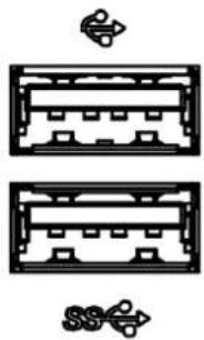
natural_image
Pure electrical circuit lines without any symbolsFigure 3.3 USB Ports
| Table 3.3: USB Ports |
| USB2.0 |
| Pin Number Description |
| 1 +5V |
| 2 DATA+ |
| 3 DATA- |
| 4 GND |
| USB3.0 |
| Pin Number Description |
| 1 +5V |
| 2 DATA+ |
| 3 DATA- |
| 4 GND |
| 5 STDA_SSRX- |
| 6 STDA_SSRX+ |
| 7 Shield GND_DRAIN |
| 8 STDA_SSTX- |
| 9 STDA_SSTX+ |
3.3.2 1 x USB3.0 OTG (Function Reserved)
Short CN 40 and pins 1-2 of CN1 to enter maskrom mode.
Table 3.4: OTG Jumper Settings
USB 3.0 OTG USB HOST
CN1 1-2 ON 3-4 ON
CN40 ON OFF
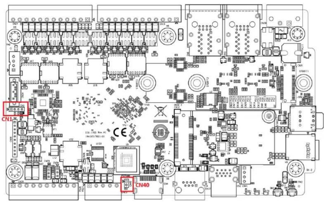
Figure 3.4 USB3.0 OTG
3.4 Console Ports
1 x RS-232 console port (RJ-45)
CONSOLE
Figure 3.5 Console Ports
Table 3.5: Console Ports
| Pin Number Description |
| 1 Not used |
| 2 Not used |
| 3 Debug Tx |
| 4 GND |
| 5 GND |
| 6 Debug Rx |
| 7 Not used |
| 8 Not used |
| Console Configuration |
| Serial Port RS-232 |
| Baud Rate 115200 |
| Parity None |
| Data Bits 8 |
| Stop Bits 1 |
| Flow Control None |
3.5 HDMI Ports
HDMI
Figure 3.6 HDMI Ports
Table 3.6: HDMI Ports
| Pin Description Pin Number Description |
| 1 HDMI1_z_DATA2+ 11 GND |
| 2 GND 12 HDMI1_z_CLK- |
| 3 HDMI1_z_DATA2- 13 HDMI1_z_CEC |
| 4 HDMI1_z_DATA1+ 14 N/A |
| 5 GND 15 HDMI1_DDC_CLK |
| 6 HDMI1_z_DATA1- 16 HDMI1_DDC_DAT |
| 7 HDMI1_z_DATA0+ 17 GND |
| 8 GND 18 +V5_HDMI |
| 9 HDMI1_z_DATA0- 19 HDMI1_HPD |
| 10 HDMI1_z_CLK+ |
3.6 CAN Ports
2 x CAN bus

Figure 3.7 CAN Ports-1
Table 3.7: CAN Ports
| Pin Description |
| Hx CAN High |
| Lx CAN Low |
| G GND |
Ports 120Ω Jumper CN26
| CAN1 | CN26(1-2) |
| CAN2 CN26(3-4) | 3 4 □ ○ ▽ 1 ○ 2 |
ON: Termination resistor connected
OFF: Termination resistor disconnected (default)
Figure 3.8 CAN Ports-2
3.7 Analog Input Ports
Do not input value over range and short unused channel to GND to avoid interfere.

Figure 3.9 Analog Input Ports
Table 3.8: Analog Input Ports
| Pin Description |
| 0/1 Analog Input |
| AGND Analog GND |
Table 3.9: Voltage/Current Jumper Settings
| Pin Status Description | |
| CN29/30 | 1-2 Voltage (Default) |
| 2-3 Current | |
Figure 3.10 Voltage/Current Jumper Settings
3.8 Serial Ports
8 x RS232/485

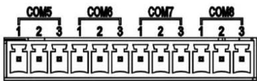
Figure 3.11 Serial Ports
Table 3.10: Serial Ports
| Pin Number | Description |
| RS-232 RS-485 | |
| 1 RX Data+ | |
| 2 TX Data- | |
| 3 GND GND |
Table 3.11: RS-232/485 Jumper Settings
| Ports Jumper RS-232 RS-485 (Default) | ||
| COM1 CN8 | 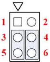 | 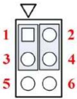 |
| COM2 CN9 | ||
| COM3 CN12 | ||
| COM4 CN14 | ||
| COM5 CN17 | ||
| COM6 CN18 | ||
| COM7 CN21 | ||
| COM8 CN22 | ||
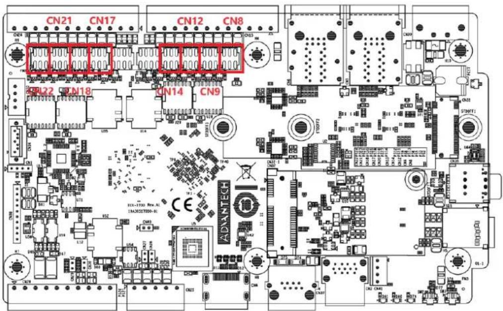
Figure 3.12 RS-232/485 Jumper Settings
Table 3.12: RS-232/485 Termination Resistors
Ports 120Ω Jumper CN13/20
| COM1 CN13(1-2) | |
| COM2 CN13(3-4) | |
| COM3 CN13(5-6) | |
| COM4 CN13(7-8) | |
| COM5 CN20(1-2) | |
| COM6 CN20(3-4) | |
| COM7 CN20(5-6) | |
| COM8 CN20(7-8) |
ON: Termination resistor connected
OFF: Termination resistor disconnected (default)
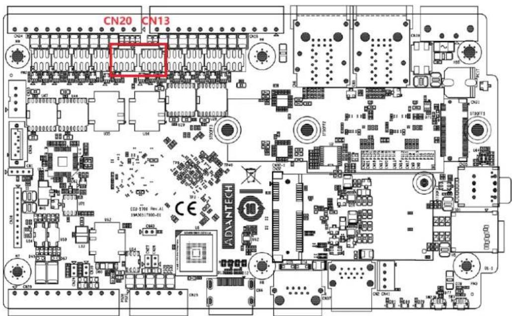
Figure 3.13 RS-232/485 Termination Resistors
3.9 Digital Inputs 0\~3 (Wet Contacts)

Figure 3.14 Digital Input 0\~3 (Wet Contacts) -1
Table 3.13: Digital Input 0\~3 (Wet Contacts)
| Pin Definition | |
| 0~3 Digital Input | Logic 1: 5~30V |
| IC Input Common | Logic 0: 0~2V |
| IGND Input Ground | |
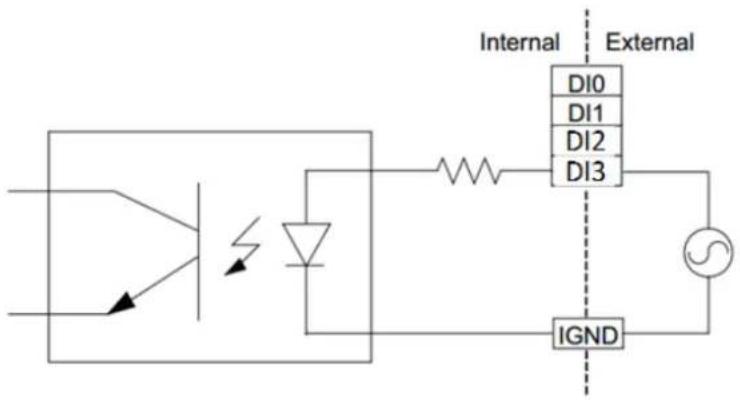
Figure 3.15 Digital Input 0\~3 (Wet Contacts) -2
3.10 Digital Inputs 4\~19 (Dry/Wet Contacts)
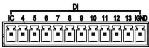
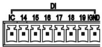
Figure 3.16 Digital Inputs 4\~19 (Dry/Wet Contacts) -1
Table 3.14: Digital Inputs 4\~19 (Dry/Wet Contacts)
| Pin Definition Wet: | ||
| 4~13,14~19 | Digital Input | Logic 1: 5~30VLogic 0: 0~2V |
| IC | Input Common | Dry:Logic 1: GroundingLogic 0: Open Circuit |
| IGND Input Ground | ||
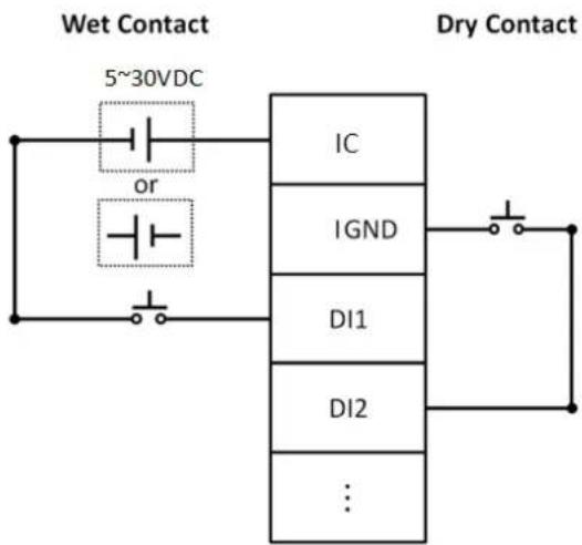
flowchart
graph TD
    A["Wet Contact"] --> B["5~30VDC"]
    B --> C["IC"]
    B --> D["IGND"]
    B --> E["DI1"]
    B --> F["DI2"]
    B --> G["..."]
    H["Dry Contact"] --> I["Ground"]
Figure 3.17 Digital Input 4\~19 (Dry/Wet Contacts) -2
3.11 Digital Output 0\~1 (Low Side Drive)

Figure 3.18 Digital Output 0\~1 (Low Side Drive) -1
Table 3.15: Digital Output 0\~1 (Low Side Drive)
| Pin Definition |
| 0~1 Digital Output |
| OC Output Common |
| OGND Output Ground |
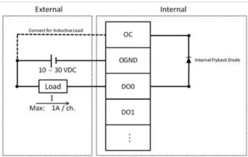
flowchart
graph TD
    A["External"] --> B["Load"]
    B --> C["10 ~ 30 VDC"]
    C --> D["Connect for Inductive Load"]
    D --> E["Internal"]
    E --> F["Internal Flyback Diode"]
    style A fill:#f9f,stroke:#333
    style E fill:#ccf,stroke:#333
    style F fill:#cfc,stroke:#333
Figure 3.19 Digital Output 0\~1 (Low Side Drive) -2
3.12 Digital Output 0\~3 (High Side Drive)
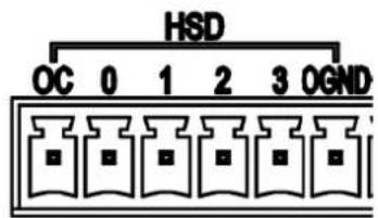
Figure 3.20 Digital Output 0\~3 (High Side Drive)
Table 3.16: Digital Output 0\~3 (High Side Drive)
| Pin Definition |
| 0~3 Digital Output |
| OC Output Common |
| OGND Output Ground |
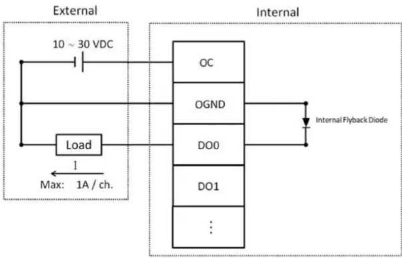
flowchart
graph TD
    A["External"] --> B["10 ~ 30 VDC"]
    B --> C["Load"]
    C --> D["Internal"]
    D --> E["Internal Flyback Diode"]
    D --> F["OC"]
    D --> G["OGND"]
    D --> H["DO0"]
    D --> I["DO1"]
    D --> J["..."]
    style A fill:#f9f,stroke:#333
    style D fill:#ccf,stroke:#333
Figure 3.21 Digital Output 0\~3 (High Side Drive)
3.13 Digital Output 0\~7 (Relay Output)
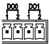
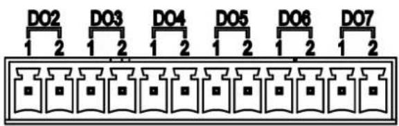
Figure 3.22 Digital Output 0\~7 (Relay Output) - 1
Table 3.17: Digital Output 0\~7 (Relay Output)
| Pin Number Definition |
| 1 NO (Normal Open) |
| 2 COM (Output Common) |
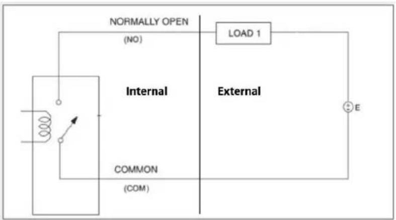
flowchart
graph TD
    A["NORMALLY OPEN (NO)"] --> B["Internal"]
    B --> C["COMMON (COM)"]
    D["LOAD 1"] --> E["External"]
    E --> F["Power Source E"]
    style A fill:#f9f,stroke:#333
    style D fill:#ccf,stroke:#333
    style E fill:#cfc,stroke:#333
Figure 3.23 Digital Output 0\~7 (Relay Output) - 2
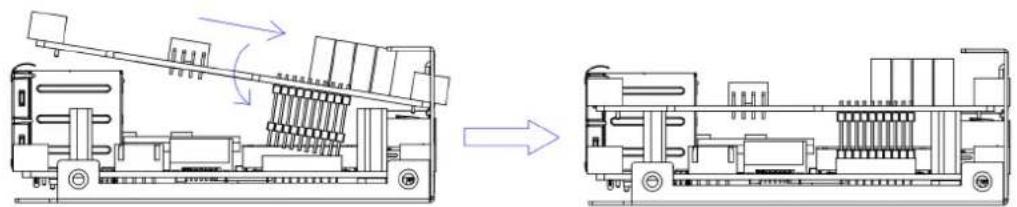
3.14 SD And SIM Slots
The ECU-1170 is equipped with 1 x full-size Mini-PCIe and 1 x M.2 B-Key socket. It also includes 1 x SD card and 2 x SIM card slots to the left side of chassis.
![[Δ] SD [Δ] SIM [Δ] SIM](/content/2026/04/729217/images/08a8a13e23393c79ccc2f04d61d581dbea37a150e8eba881b929eaeb54f63a43.jpg)
Figure 3.24 SD and SIM slots
Table 3.18: Location of Mini-PCIe and M.2 Socket
Socket Support Package
Mini-PCIe 3050/3026
M.2 B-Key 2080/3042/3052
Figure 3.25 Location of Mini-PCIe and M.2 Socket
Chapter
4
Installation
4.1 Jumper and RTC Battery Location
Disassemble the chassis and upper board to set jumpers and replace RTC battery on the lower board.
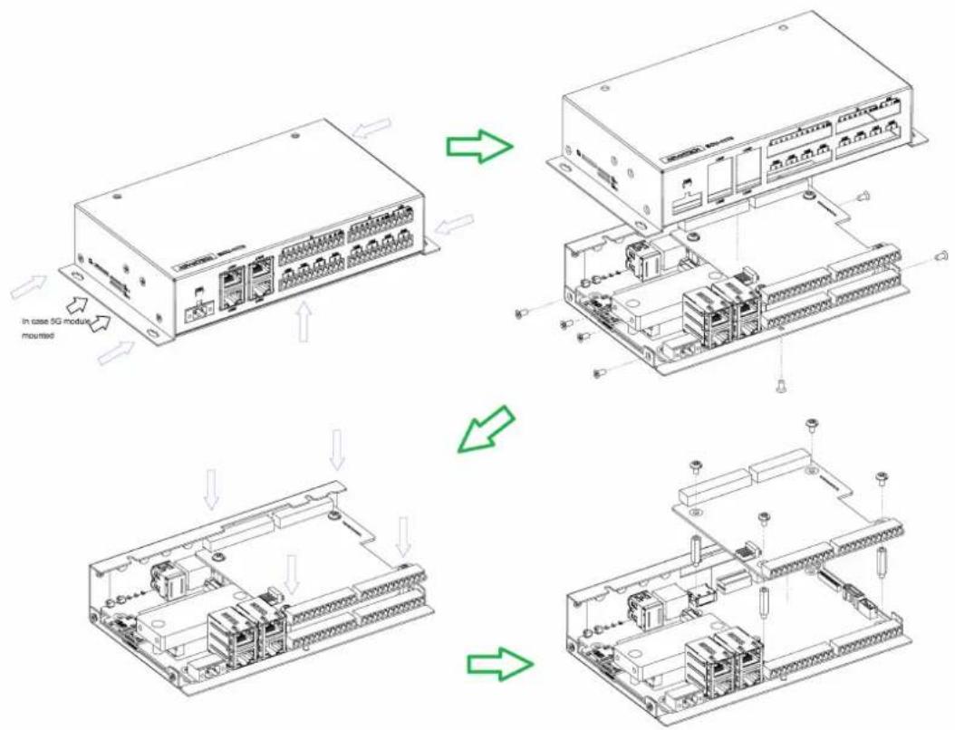
Assemble upper board
natural_image
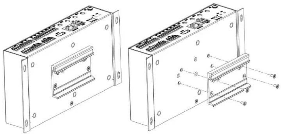
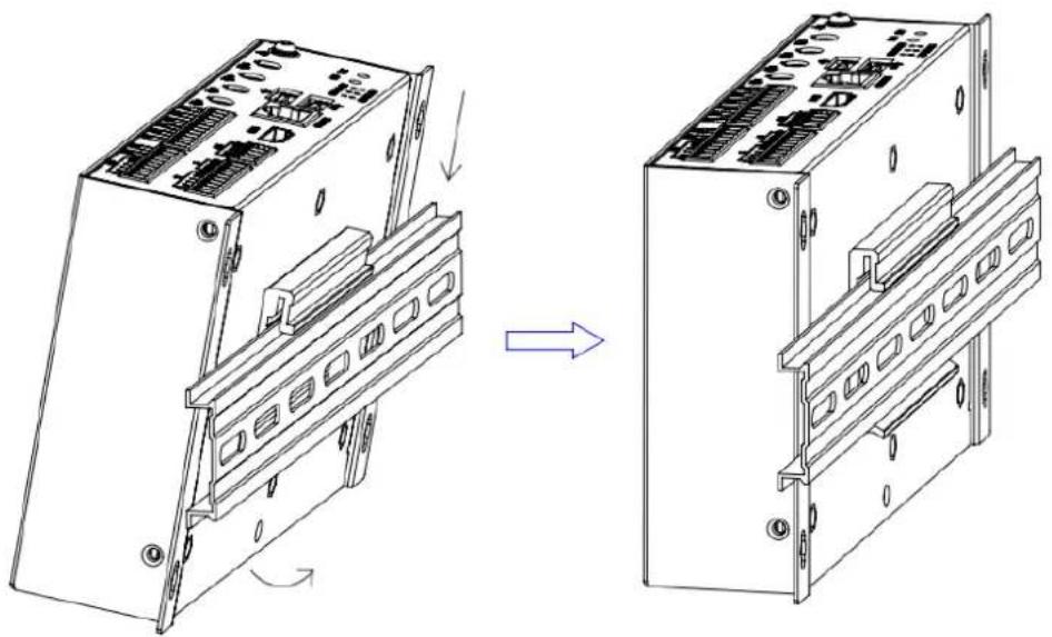
Technical line drawing of a mechanical assembly before and after assembly, showing internal components and motion indicators (no text or symbols)4.2 DIN Rail And Wall Mount Installation
The wall mount bracket is built-in with the chassis and Din rail is also offered in accessories.
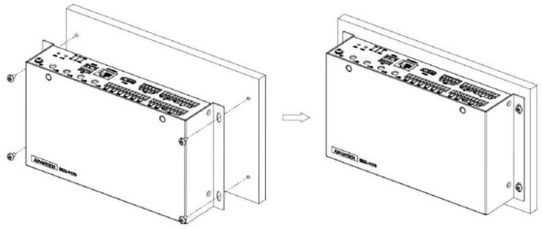
To mount the wall plate, use screws of the size M4*6Lmm min, 4pcs.
natural_image
Technical line drawings of two electronic device modules with mounting holes and internal components (no text or symbols)DIN rail mounting screws (4pcs, M3x6L).
natural_image
Technical line drawing of a server rack with internal components, showing assembly before and after transformation (no text or symbols)4.3 Module Installation
4.3.1 M.2 Slot Module Assembly
The M.2 slot supports 2280/2242/3042 modules. In the case of 2242/3042, an adapter is needed. The set of the adapter and screws in the below table is the customer's PO. The set of post and screws is within the BOM of shipment and pre-installed. In the case of 2280, the IO board needs to be removed before installation
Table 4.1: M.2 Slot Module Assembly
Part Number Description
1960102502T000 Adapter
19350304A0 Screw
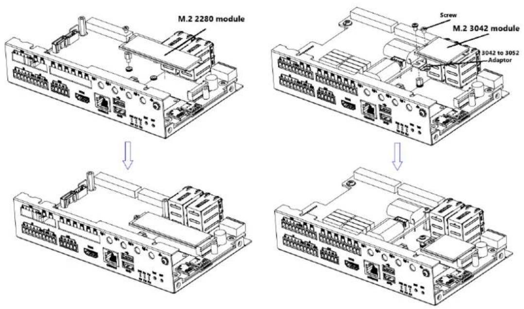
Figure 4.1 M.2 Slot Module Assembly
4.3.2 5G Module Assembly
- Remove the top cover and place rubber under the 5G module for better support.
- Assembly the 5G module, thermal pad, and thermal bracket.
- Remove two plugs from the top cover. Then assemble the top cover and connect the thermal bracket with the chassis with two screws for better heat dissipation.
The set of thermal accessories and screws in the below table are upon customer's PO.
Table 4.2: 5G Module Assembly
| Part Number Description |
| 1960116055N001 5G thermal bracket |
| 1990042003N000 Support rubber |
| 1990042007N000 Thermal pad |
| 1930007459-01 Screw for thermal bracket |
| 1930000071 Screw for 5G thermal bracket connected chassis |
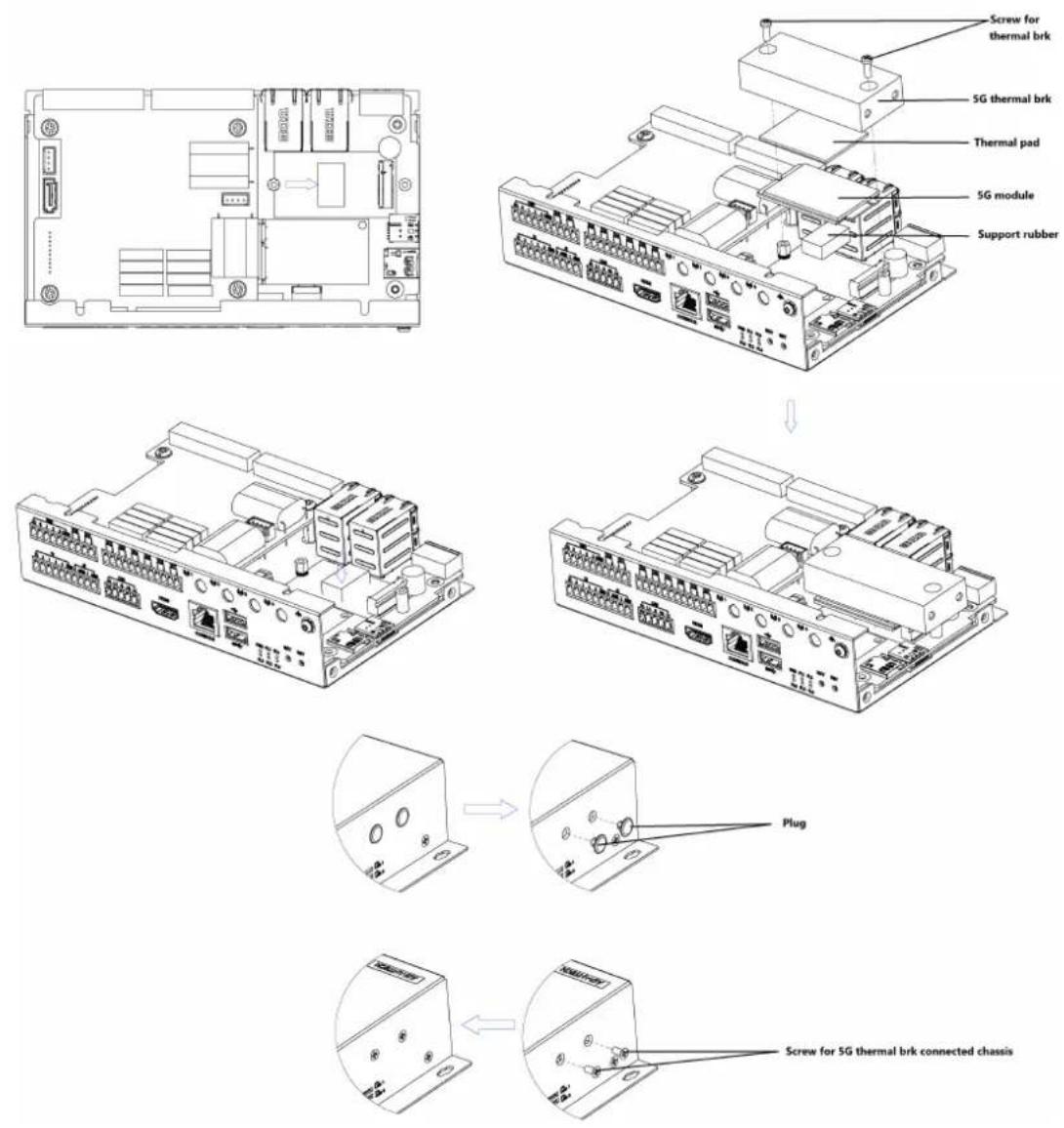
Figure 4.2 5G Module Assembly
4.3.3 Mini-PCIe Slot Module Assembly
The Mini-PCIe slot is compatible with the M.2 E-Key module using an adapter. The set of adapter and screw in the below table is upon the customer's PO. The screw for the adapter is pre-installed.
Table 4.3: Mini-PCIe Slot Module Assembly
Part Number Description
EXM-CMPF1-M2E01E M.2 E-Key to mPCIe adapter board
1930000016 Screw
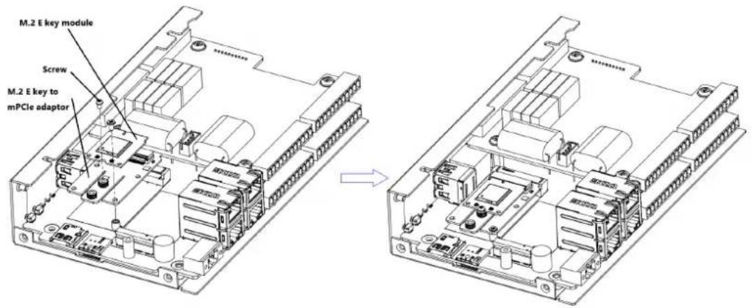
Figure 4.3 Mini-PCIe Slot Module Assembly
www.advantech.com
Please verify specifications before quoting. This guide is intended for reference purposes only.
All product specifications are subject to change without notice.
No part of this publication may be reproduced in any form or by any means, electronic, photocopying, recording or otherwise, without prior written permission of the publisher.
All brand and product names are trademarks or registered trademarks of their respective companies.
© Advantech Co., Ltd. 2025
- ECU-1170
- Copyright
- Acknowledgments
- Support
- Declaration of Conformity
- CE
- FCC Class A
- Technical Support and Assistance
- Safety Precaution - Static Electricity
- Safety Instructions
- Chapter 2 Hardware Functionality......7
- Chapter 3 Pins, Jumper Settings, and Wiring ..11
- Chapter 4 Installation
- Chapter 1
- Introduction
- Specifications
- General
- System
- I/O Interfaces
- Edgelink\*
- Software Configurations
- Chassis Dimensions
- Packing List
- Chapter 2
- Overview
- LED Status Indicators and Buttons
- System Status Indicators
- Ethernet Status Indicators
- System Button
- Chapter 3
- Power Supply
- DC-In Connector Wiring
- Ethernet Ports
- USB Ports
- 1 x USB2.0 HOST, 1 x USB3.0 HOST
- 1 x USB3.0 OTG (Function Reserved)
- Console Ports
- HDMI Ports
- CAN Ports
- Analog Input Ports
- Serial Ports
- Digital Inputs 0\~3 (Wet Contacts)
- Digital Inputs 4\~19 (Dry/Wet Contacts)
- Digital Output 0\~1 (Low Side Drive)
- Digital Output 0\~3 (High Side Drive)
- Digital Output 0\~7 (Relay Output)
- SD And SIM Slots
- Chapter
- 4
- Jumper and RTC Battery Location
- DIN Rail And Wall Mount Installation
- Module Installation
- M.2 Slot Module Assembly
- 5G Module Assembly
- Mini-PCIe Slot Module Assembly
- www.advantech.com
Brand : Advantech
Model : ECU-1170
Category : Industrial electronics